Embed Size (px)
Citation preview
This content has been downloaded from IOPscience. Please scroll down to see the full text.
Download details:
IP Address: 86.145.203.223
This content was downloaded on 04/05/2014 at 10:32
Please note that terms and conditions apply.
Preferential elimination of metallic single-walled carbon nanotubes using microwave
irradiation
View the table of contents for this issue, or go to the journal homepage for more
2009 Nanotechnology 20 065707
(http://iopscience.iop.org/0957-4484/20/6/065707)
Home Search Collections Journals About Contact us My IOPscience
IOP PUBLISHING NANOTECHNOLOGY
Nanotechnology 20 (2009) 065707 (5pp) doi:10.1088/0957-4484/20/6/065707
Preferential elimination of metallicsingle-walled carbon nanotubes usingmicrowave irradiationHyung Cheoul Shim1,2, Jin-Won Song2, Yoon Keun Kwak1,Soohyun Kim1,3 and Chang-Soo Han2,3
1 School of Mechanical, Aerospace and Systems Engineering, Department of MechanicalEngineering, Korea Advanced Institute of Science and Technology (KAIST), 373-1,Guseong-dong, Yuseong-gu, Daejeon 305-701, Republic of Korea2 Nano Mechanical Systems Research Center, Korea Institute of Machinery and Materials(KIMM), 171 Jang-dong, Yousung-gu, Daejeon 305-343, Republic of Korea
E-mail: [email protected] (S Kim) and [email protected] (C-S Han)
Received 22 October 2008, in final form 24 November 2008Published 15 January 2009Online at stacks.iop.org/Nano/20/065707
AbstractThis study presents a simple, easy and rapid technique for the preferential destruction ofmetallic single-walled carbon nanotubes (m-SWNTs) using microwave irradiation. Theproportion of m-SWNTs in a randomly networked film that were made of pristine SWNTs wasgradually reduced with microwave irradiation of 1000 W at 2.45 GHz ranging from 0 to 20 min.Additionally it was observed that the m-SWNTs with a higher chiral angle were destroyed first.The Raman spectra and drain current–gate voltage characteristics curve show that this methodfacilitated the selective removal of m-SWNTs.
(Some figures in this article are in colour only in the electronic version)
1. Introduction
Although there has been rapid progress in research into carbonnanotubes (CNTs) since they were discovered in 1991 [1],the irregular properties of CNTs, including the ranges of theirdiameters and lengths as well as their degree of chirality,continues to impede the progression of this technology to massproduction of CNT-related products. In particular, the useof single-walled carbon nanotubes (SWNTs) as the buildingblocks of nanoscale electronic devices [2–8] has attractedmuch attention due to their semiconducting properties.
For these applications, it is most important to extract onlysemiconducting single-walled carbon nanotubes (s-SWNTs)from a collection of pristine SWNTs that includes bothmetallic and semiconducting nanotubes. A selective separationprocess would be helpful not only to maximize the uniqueelectrical properties of SWNTs, such as their high current-carrying density [5], high mobility [9] and ballistic transportproperties [10], but also to guarantee the repeatability andclarity of analyses of characteristics during experiments. For
3 Authors to whom any correspondence should be addressed.
this reason, many papers on the sorting of SWNTs havebeen published recently [11–27]. However, most of themcontain complex physical or chemical processes which havethe potential to damage or contaminate pristine samples.Moreover, the explanations of the yield and the time requiredto complete the separation are not always clear. Several recentresearch reports [23–27] have shown the possibility of bulkselective sorting of SWNTs through various methods. In thepresent study, the selective destruction of metallic SWNTs (m-SWNTs) in a randomly networked SWNT film was attemptedusing microwave irradiation based on the different dielectricconstants of m-SWNTs and s-SWNTs. During microwaveprocessing, energy is directly supplied to the material by anelectromagnetic field. Consequently, this type of volumetricheating can reduce the processing time and save energycompared to other heating methods. In addition, microwaveirradiation allows the discriminative heating of materials withdifferent dielectric constants. In other words, the microwaveswill selectively couple with higher loss materials in a mannerthat depends on the dielectric constant [28]. If the electric fieldis assumed to be uniform throughout the volume, the power
0957-4484/09/065707+05$30.00 © 2009 IOP Publishing Ltd Printed in the UK1
Nanotechnology 20 (2009) 065707 H C Shim et al
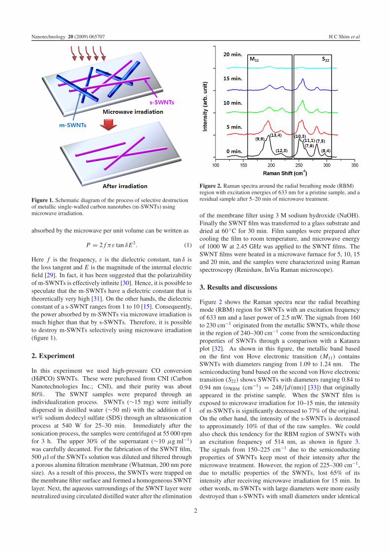
Figure 1. Schematic diagram of the process of selective destructionof metallic single-walled carbon nanotubes (m-SWNTs) usingmicrowave irradiation.
absorbed by the microwave per unit volume can be written as
P = 2 f πε tan δE2. (1)
Here f is the frequency, ε is the dielectric constant, tan δ isthe loss tangent and E is the magnitude of the internal electricfield [29]. In fact, it has been suggested that the polarizabilityof m-SWNTs is effectively infinite [30]. Hence, it is possible tospeculate that the m-SWNTs have a dielectric constant that istheoretically very high [31]. On the other hands, the dielectricconstant of a s-SWNT ranges from 1 to 10 [15]. Consequently,the power absorbed by m-SWNTs via microwave irradiation ismuch higher than that by s-SWNTs. Therefore, it is possibleto destroy m-SWNTs selectively using microwave irradiation(figure 1).
2. Experiment
In this experiment we used high-pressure CO conversion(HiPCO) SWNTs. These were purchased from CNI (CarbonNanotechnologies Inc.; CNI), and their purity was about80%. The SWNT samples were prepared through anindividualization process. SWNTs (∼15 mg) were initiallydispersed in distilled water (∼50 ml) with the addition of 1wt% sodium dodecyl sulfate (SDS) through an ultrasonicationprocess at 540 W for 25–30 min. Immediately after thesonication process, the samples were centrifuged at 55 000 rpmfor 3 h. The upper 30% of the supernatant (∼10 μg ml−1)was carefully decanted. For the fabrication of the SWNT film,500 μl of the SWNTs solution was diluted and filtered througha porous alumina filtration membrane (Whatman, 200 nm poresize). As a result of this process, the SWNTs were trapped onthe membrane filter surface and formed a homogeneous SWNTlayer. Next, the aqueous surroundings of the SWNT layer wereneutralized using circulated distilled water after the elimination
Figure 2. Raman spectra around the radial breathing mode (RBM)region with excitation energies of 633 nm for a pristine sample, and aresidual sample after 5–20 min of microwave treatment.
of the membrane filter using 3 M sodium hydroxide (NaOH).Finally the SWNT film was transferred to a glass substrate anddried at 60 ◦C for 30 min. Film samples were prepared aftercooling the film to room temperature, and microwave energyof 1000 W at 2.45 GHz was applied to the SWNT films. TheSWNT films were heated in a microwave furnace for 5, 10, 15and 20 min, and the samples were characterized using Ramanspectroscopy (Renishaw, InVia Raman microscope).
3. Results and discussions
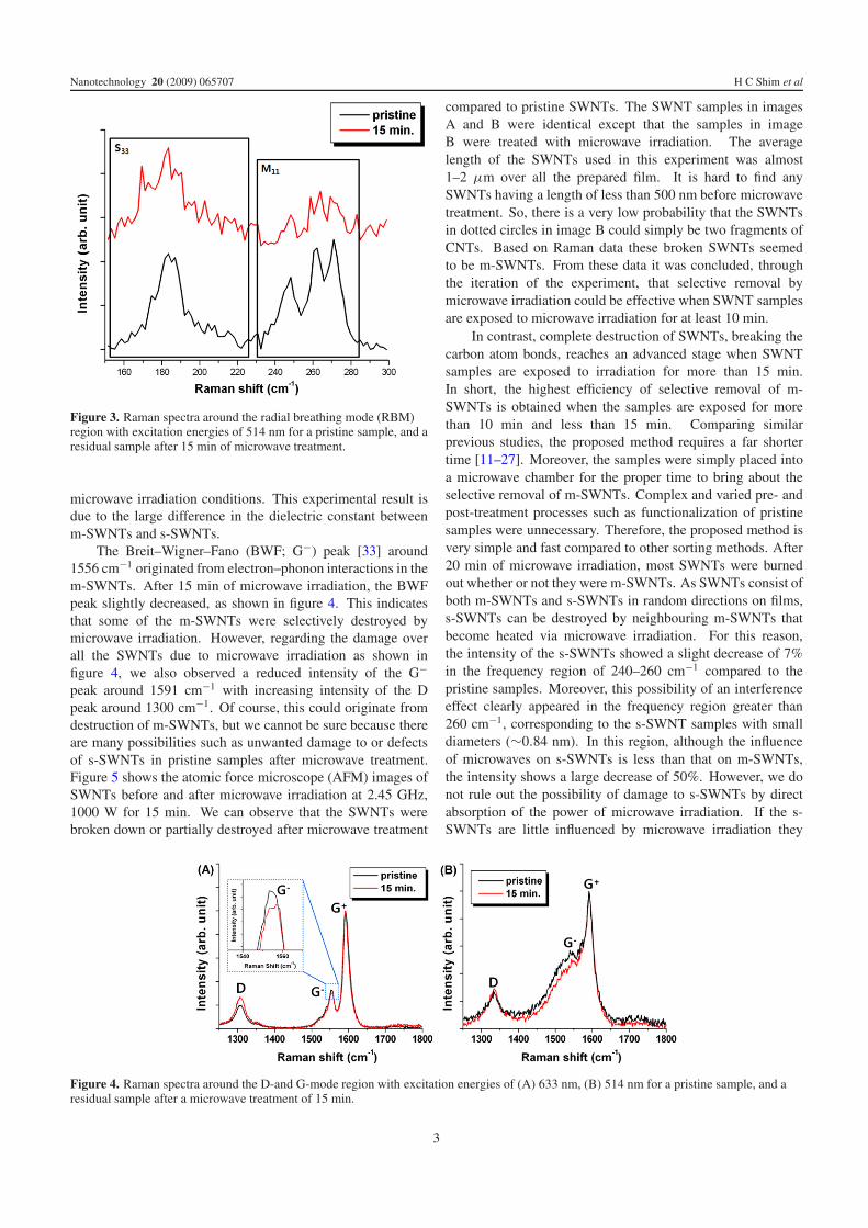
Figure 2 shows the Raman spectra near the radial breathingmode (RBM) region for SWNTs with an excitation frequencyof 633 nm and a laser power of 2.5 mW. The signals from 160to 230 cm−1 originated from the metallic SWNTs, while thosein the region of 240–300 cm−1 come from the semiconductingproperties of SWNTs through a comparison with a Katauraplot [32]. As shown in this figure, the metallic band basedon the first von Hove electronic transition (M11) containsSWNTs with diameters ranging from 1.09 to 1.24 nm. Thesemiconducting band based on the second von Hove electronictransition (S22) shows SWNTs with diameters ranging 0.84 to0.94 nm (ωRBM (cm−1) = 248/[d(nm)] [33]) that originallyappeared in the pristine sample. When the SWNT film isexposed to microwave irradiation for 10–15 min, the intensityof m-SWNTs is significantly decreased to 77% of the original.On the other hand, the intensity of the s-SWNTs is decreasedto approximately 10% of that of the raw samples. We couldalso check this tendency for the RBM region of SWNTs withan excitation frequency of 514 nm, as shown in figure 3.The signals from 150–225 cm−1 due to the semiconductingproperties of SWNTs keep most of their intensity after themicrowave treatment. However, the region of 225–300 cm−1,due to metallic properties of the SWNTs, lost 65% of itsintensity after receiving microwave irradiation for 15 min. Inother words, m-SWNTs with large diameters were more easilydestroyed than s-SWNTs with small diameters under identical
2
Nanotechnology 20 (2009) 065707 H C Shim et al
Figure 3. Raman spectra around the radial breathing mode (RBM)region with excitation energies of 514 nm for a pristine sample, and aresidual sample after 15 min of microwave treatment.
microwave irradiation conditions. This experimental result isdue to the large difference in the dielectric constant betweenm-SWNTs and s-SWNTs.
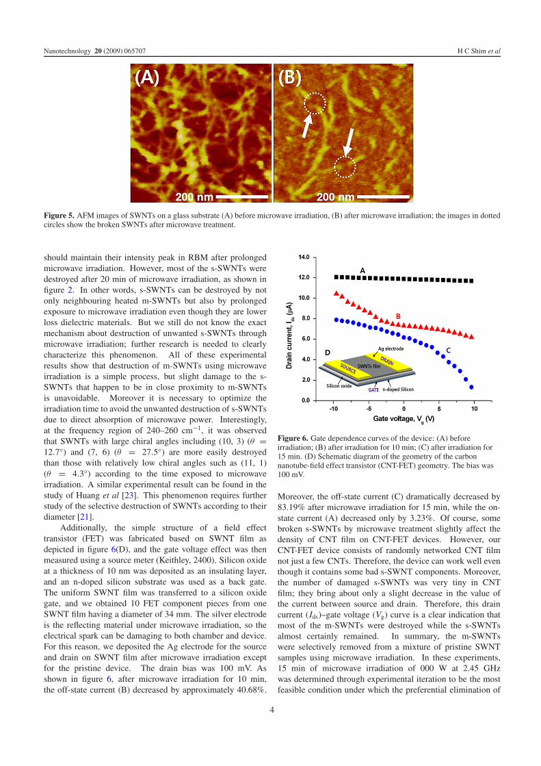
The Breit–Wigner–Fano (BWF; G−) peak [33] around1556 cm−1 originated from electron–phonon interactions in them-SWNTs. After 15 min of microwave irradiation, the BWFpeak slightly decreased, as shown in figure 4. This indicatesthat some of the m-SWNTs were selectively destroyed bymicrowave irradiation. However, regarding the damage overall the SWNTs due to microwave irradiation as shown infigure 4, we also observed a reduced intensity of the G−peak around 1591 cm−1 with increasing intensity of the Dpeak around 1300 cm−1. Of course, this could originate fromdestruction of m-SWNTs, but we cannot be sure because thereare many possibilities such as unwanted damage to or defectsof s-SWNTs in pristine samples after microwave treatment.Figure 5 shows the atomic force microscope (AFM) images ofSWNTs before and after microwave irradiation at 2.45 GHz,1000 W for 15 min. We can observe that the SWNTs werebroken down or partially destroyed after microwave treatment
compared to pristine SWNTs. The SWNT samples in imagesA and B were identical except that the samples in imageB were treated with microwave irradiation. The averagelength of the SWNTs used in this experiment was almost1–2 μm over all the prepared film. It is hard to find anySWNTs having a length of less than 500 nm before microwavetreatment. So, there is a very low probability that the SWNTsin dotted circles in image B could simply be two fragments ofCNTs. Based on Raman data these broken SWNTs seemedto be m-SWNTs. From these data it was concluded, throughthe iteration of the experiment, that selective removal bymicrowave irradiation could be effective when SWNT samplesare exposed to microwave irradiation for at least 10 min.
In contrast, complete destruction of SWNTs, breaking thecarbon atom bonds, reaches an advanced stage when SWNTsamples are exposed to irradiation for more than 15 min.In short, the highest efficiency of selective removal of m-SWNTs is obtained when the samples are exposed for morethan 10 min and less than 15 min. Comparing similarprevious studies, the proposed method requires a far shortertime [11–27]. Moreover, the samples were simply placed intoa microwave chamber for the proper time to bring about theselective removal of m-SWNTs. Complex and varied pre- andpost-treatment processes such as functionalization of pristinesamples were unnecessary. Therefore, the proposed method isvery simple and fast compared to other sorting methods. After20 min of microwave irradiation, most SWNTs were burnedout whether or not they were m-SWNTs. As SWNTs consist ofboth m-SWNTs and s-SWNTs in random directions on films,s-SWNTs can be destroyed by neighbouring m-SWNTs thatbecome heated via microwave irradiation. For this reason,the intensity of the s-SWNTs showed a slight decrease of 7%in the frequency region of 240–260 cm−1 compared to thepristine samples. Moreover, this possibility of an interferenceeffect clearly appeared in the frequency region greater than260 cm−1, corresponding to the s-SWNT samples with smalldiameters (∼0.84 nm). In this region, although the influenceof microwaves on s-SWNTs is less than that on m-SWNTs,the intensity shows a large decrease of 50%. However, we donot rule out the possibility of damage to s-SWNTs by directabsorption of the power of microwave irradiation. If the s-SWNTs are little influenced by microwave irradiation they
Figure 4. Raman spectra around the D-and G-mode region with excitation energies of (A) 633 nm, (B) 514 nm for a pristine sample, and aresidual sample after a microwave treatment of 15 min.
3
Nanotechnology 20 (2009) 065707 H C Shim et al
Figure 5. AFM images of SWNTs on a glass substrate (A) before microwave irradiation, (B) after microwave irradiation; the images in dottedcircles show the broken SWNTs after microwave treatment.
should maintain their intensity peak in RBM after prolongedmicrowave irradiation. However, most of the s-SWNTs weredestroyed after 20 min of microwave irradiation, as shown infigure 2. In other words, s-SWNTs can be destroyed by notonly neighbouring heated m-SWNTs but also by prolongedexposure to microwave irradiation even though they are lowerloss dielectric materials. But we still do not know the exactmechanism about destruction of unwanted s-SWNTs throughmicrowave irradiation; further research is needed to clearlycharacterize this phenomenon. All of these experimentalresults show that destruction of m-SWNTs using microwaveirradiation is a simple process, but slight damage to the s-SWNTs that happen to be in close proximity to m-SWNTsis unavoidable. Moreover it is necessary to optimize theirradiation time to avoid the unwanted destruction of s-SWNTsdue to direct absorption of microwave power. Interestingly,at the frequency region of 240–260 cm−1, it was observedthat SWNTs with large chiral angles including (10, 3) (θ =12.7◦) and (7, 6) (θ = 27.5◦) are more easily destroyedthan those with relatively low chiral angles such as (11, 1)(θ = 4.3◦) according to the time exposed to microwaveirradiation. A similar experimental result can be found in thestudy of Huang et al [23]. This phenomenon requires furtherstudy of the selective destruction of SWNTs according to theirdiameter [21].
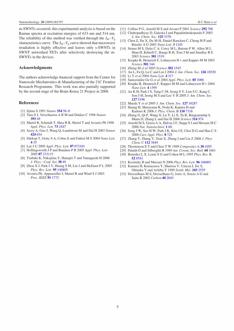
Additionally, the simple structure of a field effecttransistor (FET) was fabricated based on SWNT film asdepicted in figure 6(D), and the gate voltage effect was thenmeasured using a source meter (Keithley, 2400). Silicon oxideat a thickness of 10 nm was deposited as an insulating layer,and an n-doped silicon substrate was used as a back gate.The uniform SWNT film was transferred to a silicon oxidegate, and we obtained 10 FET component pieces from oneSWNT film having a diameter of 34 mm. The silver electrodeis the reflecting material under microwave irradiation, so theelectrical spark can be damaging to both chamber and device.For this reason, we deposited the Ag electrode for the sourceand drain on SWNT film after microwave irradiation exceptfor the pristine device. The drain bias was 100 mV. Asshown in figure 6, after microwave irradiation for 10 min,the off-state current (B) decreased by approximately 40.68%.
Figure 6. Gate dependence curves of the device: (A) beforeirradiation; (B) after irradiation for 10 min; (C) after irradiation for15 min. (D) Schematic diagram of the geometry of the carbonnanotube-field effect transistor (CNT-FET) geometry. The bias was100 mV.
Moreover, the off-state current (C) dramatically decreased by83.19% after microwave irradiation for 15 min, while the on-state current (A) decreased only by 3.23%. Of course, somebroken s-SWNTs by microwave treatment slightly affect thedensity of CNT film on CNT-FET devices. However, ourCNT-FET device consists of randomly networked CNT filmnot just a few CNTs. Therefore, the device can work well eventhough it contains some bad s-SWNT components. Moreover,the number of damaged s-SWNTs was very tiny in CNTfilm; they bring about only a slight decrease in the value ofthe current between source and drain. Therefore, this draincurrent (Ids)–gate voltage (Vg) curve is a clear indication thatmost of the m-SWNTs were destroyed while the s-SWNTsalmost certainly remained. In summary, the m-SWNTswere selectively removed from a mixture of pristine SWNTsamples using microwave irradiation. In these experiments,15 min of microwave irradiation of 000 W at 2.45 GHzwas determined through experimental iteration to be the mostfeasible condition under which the preferential elimination of
4
Nanotechnology 20 (2009) 065707 H C Shim et al
m-SWNTs occurred; this experimental analysis is based on theRaman spectra at excitation energies of 633 nm and 514 nm.The reliability of this method was verified through the Ids–Vg
characteristics curve. The Ids–Vg curve showed that microwaveirradiation is highly effective and leaves only s-SWNTs inSWNT networked FETs after selectively destroying the m-SWNTs in the devices.
Acknowledgments
The authors acknowledge financial support from the Center forNanoscale Mechatronics & Manufacturing of the 21C FrontierResearch Programme. This work was also partially supportedby the second stage of the Brain Korea 21 Project in 2008.
References
[1] Iijima S 1991 Nature 354 56–8[2] Tans S J, Verschueren A R M and Dekker C 1998 Nature
393 49[3] Martel R, Schmidt T, Shea H R, Hertel T and Avouris Ph 1998
Appl. Phys. Lett. 73 2447[4] Javey A, Guo J, Wang Q, Lundstrom M and Dai H 2003 Nature
424 654[5] Durkop T, Getty S A, Cobas E and Fuhrer M S 2004 Nano Lett.
4 35[6] Lee J U 2005 Appl. Phys. Lett. 87 073101[7] Hollingsworth J P and Bandaru P R 2005 Appl. Phys. Lett.
2005 87 233115[8] Tsubaki K, Nakajima Y, Hanajiri T and Yamaguchi H 2006
J. Phys.: Conf. Ser. 38 49[9] Zhou X J, Park J Y, Huang S M, Liu J and McEuen P L 2005
Phys. Rev. Lett. 95 146805[10] Avouris Ph, Appenzeller J, Martel R and Wind S J 2003
Proc. IEEE 91 1772
[11] Collins P G, Arnold M S and Avouri P 2001 Science 292 706[12] Chattopadhyay D, Galeska I and Papadimitrakopoulo F 2003
J. Am. Chem. Soc. 125 3370[13] Chen Z, Du X, Du M-H, Daniel Rancken C, Cheng H-P and
Rinzler A G 2003 Nano Lett. 3 1245[14] Strano M S, Dyke C A, Usrey M L, Barone P W, Allen M J,
Shan H, Kittrell C, Hauge R H, Tour J M and Smalley R E2003 Science 301 1519
[15] Krupke R, Hennrich F, Lohneysen H v and Kappes M M 2003Science 301 344
[16] Zheng M et al 2003 Science 302 1545[17] An L, Fu Q, Lu C and Liu J 2004 J. Am. Chem. Soc. 126 10520[18] Li Y et al 2004 Nano Lett. 4 317[19] Samsonidze Ge G et al 2004 Appl. Phys. Lett. 85 1006[20] Krupke R, Hennrich F, Kappes M M and Lohneysen H v 2004
Nano Lett. 4 1395[21] An K H, Park J S, Yang C-M, Jeong S Y, Lim S C, Kang C,
Son J-H, Jeong M S and Lee Y H 2005 J. Am. Chem. Soc.127 5196
[22] Maeda Y et al 2005 J. Am. Chem. Soc. 127 10287[23] Huang H, Maruyama R, Noda K, Kajiura H and
Kadono K 2006 J. Phys. Chem. B 110 7316[24] Zhang G, Qi P, Wang X, Lu Y, Li X, Tu R, Bangsaruntip S,
Mann D, Zhang L and Dai H 2006 Science 314 974[25] Arnold M S, Green A A, Hulvat J F, Stupp S I and Hersam M C
2006 Nat. Nanotechnol. 1 60[26] Song J W, Seo H W, Park J K, Kim J E, Choi D G and Han C S
2008 Curr. Appl. Phys. 8 725[27] Zhang Y, Zhang Y, Xian X, Zhang J and Liu Z 2008 J. Phys.
Chem. C 112 3849[28] Thostenson E T and Chou T W 1999 Composites A 30 1055[29] Palaith D and Silberglitt R 1989 Am. Ceram. Soc. Bull. 68 1601[30] Benedict L X, Louie S G and Cohen M L 1995 Phys. Rev. B
52 8541[31] Kozinsky B and Marzari N 2006 Phys. Rev. Lett. 96 166801[32] Kataura H, Kumazawa Y, Maniwa Y, Umezu I, Six S,
Ohtsuka Y and Achiba Y 1999 Synth. Met. 103 2555[33] Dresselhaus M S, Dresselhaus G, Jorio A, Souza A G and
Saito R 2002 Carbon 40 2043
5


![Double-walled carbon nanotubes: synthesis, structural ...077-088]-01.pdf · Double-walled carbon nanotubes: synthesis, structural characterization, and ... are seamless cylindrical](https://img.pdfslide.us/doc/110x75/5aa2b5537f8b9ac67a8d717c/double-walled-carbon-nanotubes-synthesis-structural-077-088-01pdfdouble-walled.jpg)