Embed Size (px)
Citation preview
1
1
Precision Low-Level
Measurement Design
2
2
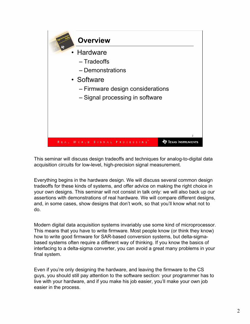
Overview
• Hardware
– Tradeoffs
– Demonstrations
• Software
– Firmware design considerations
– Signal processing in software
This seminar will discuss design tradeoffs and techniques for analog-to-digital data
acquisition circuits for low-level, high-precision signal measurement.
Everything begins in the hardware design. We will discuss several common design
tradeoffs for these kinds of systems, and offer advice on making the right choice in
your own designs. This seminar will not consist in talk only: we will also back up our
assertions with demonstrations of real hardware. We will compare different designs,
and, in some cases, show designs that don’t work, so that you’ll know what not to
do.
Modern digital data acquisition systems invariably use some kind of microprocessor.
This means that you have to write firmware. Most people know (or think they know)
how to write good firmware for SAR-based conversion systems, but delta-sigma-
based systems often require a different way of thinking. If you know the basics of
interfacing to a delta-sigma converter, you can avoid a great many problems in your
final system.
Even if you’re only designing the hardware, and leaving the firmware to the CS
guys, you should still pay attention to the software section: your programmer has to
live with your hardware, and if you make his job easier, you’ll make your own job
easier in the process.
3
3
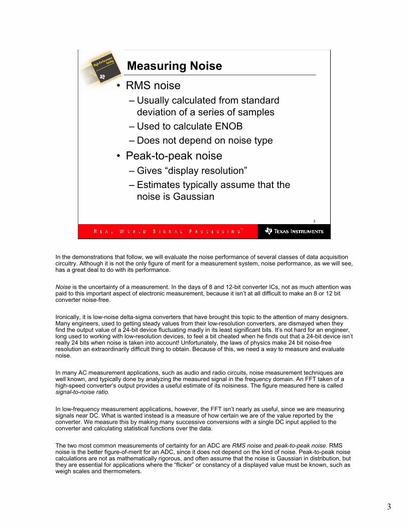
Measuring Noise
• RMS noise
– Usually calculated from standard
deviation of a series of samples
– Used to calculate ENOB
– Does not depend on noise type
• Peak-to-peak noise
– Gives “display resolution”
– Estimates typically assume that the
noise is Gaussian
In the demonstrations that follow, we will evaluate the noise performance of several classes of data acquisition circuitry. Although it is not the only figure of merit for a measurement system, noise performance, as we will see, has a great deal to do with its performance.
Noise is the uncertainty of a measurement. In the days of 8 and 12-bit converter ICs, not as much attention was paid to this important aspect of electronic measurement, because it isn’t at all difficult to make an 8 or 12 bit converter noise-free.
Ironically, it is low-noise delta-sigma converters that have brought this topic to the attention of many designers. Many engineers, used to getting steady values from their low-resolution converters, are dismayed when they find the output value of a 24-bit device fluctuating madly in its least significant bits. It’s not hard for an engineer, long used to working with low-resolution devices, to feel a bit cheated when he finds out that a 24-bit device isn’t really 24 bits when noise is taken into account! Unfortunately, the laws of physics make 24 bit noise-free resolution an extraordinarily difficult thing to obtain. Because of this, we need a way to measure and evaluate noise.
In many AC measurement applications, such as audio and radio circuits, noise measurement techniques are well known, and typically done by analyzing the measured signal in the frequency domain. An FFT taken of a high-speed converter’s output provides a useful estimate of its noisiness. The figure measured here is called signal-to-noise ratio.
In low-frequency measurement applications, however, the FFT isn’t nearly as useful, since we are measuring signals near DC. What is wanted instead is a measure of how certain we are of the value reported by the converter. We measure this by making many successive conversions with a single DC input applied to the converter and calculating statistical functions over the data.
The two most common measurements of certainty for an ADC are RMS noise and peak-to-peak noise. RMS noise is the better figure-of-merit for an ADC, since it does not depend on the kind of noise. Peak-to-peak noise calculations are not as mathematically rigorous, and often assume that the noise is Gaussian in distribution, but they are essential for applications where the “flicker” or constancy of a displayed value must be known, such as weigh scales and thermometers.
4
4
Measuring Noise
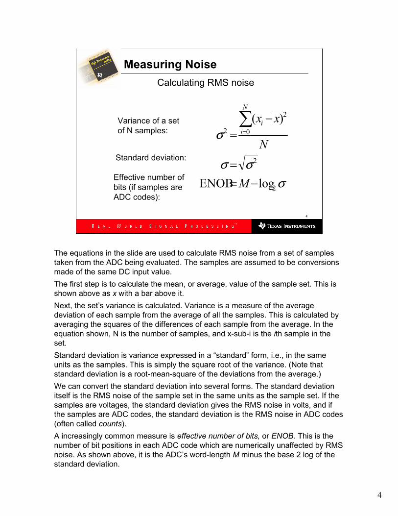
Calculating RMS noise
σ
σσ
σ
2
2
0
2
2
log ENOB
)(
−=
=
−
=
∑=
M
N
xxN
i
iVariance of a set
of N samples:
Standard deviation:
Effective number of
bits (if samples are
ADC codes):
The equations in the slide are used to calculate RMS noise from a set of samples
taken from the ADC being evaluated. The samples are assumed to be conversions
made of the same DC input value.
The first step is to calculate the mean, or average, value of the sample set. This is
shown above as x with a bar above it.
Next, the set’s variance is calculated. Variance is a measure of the average
deviation of each sample from the average of all the samples. This is calculated by
averaging the squares of the differences of each sample from the average. In the
equation shown, N is the number of samples, and x-sub-i is the ith sample in the
set.
Standard deviation is variance expressed in a “standard” form, i.e., in the same
units as the samples. This is simply the square root of the variance. (Note that
standard deviation is a root-mean-square of the deviations from the average.)
We can convert the standard deviation into several forms. The standard deviation
itself is the RMS noise of the sample set in the same units as the sample set. If the
samples are voltages, the standard deviation gives the RMS noise in volts, and if
the samples are ADC codes, the standard deviation is the RMS noise in ADC codes
(often called counts).
A increasingly common measure is effective number of bits, or ENOB. This is the
number of bit positions in each ADC code which are numerically unaffected by RMS
noise. As shown above, it is the ADC’s word-length M minus the base 2 log of the
standard deviation.
5
5
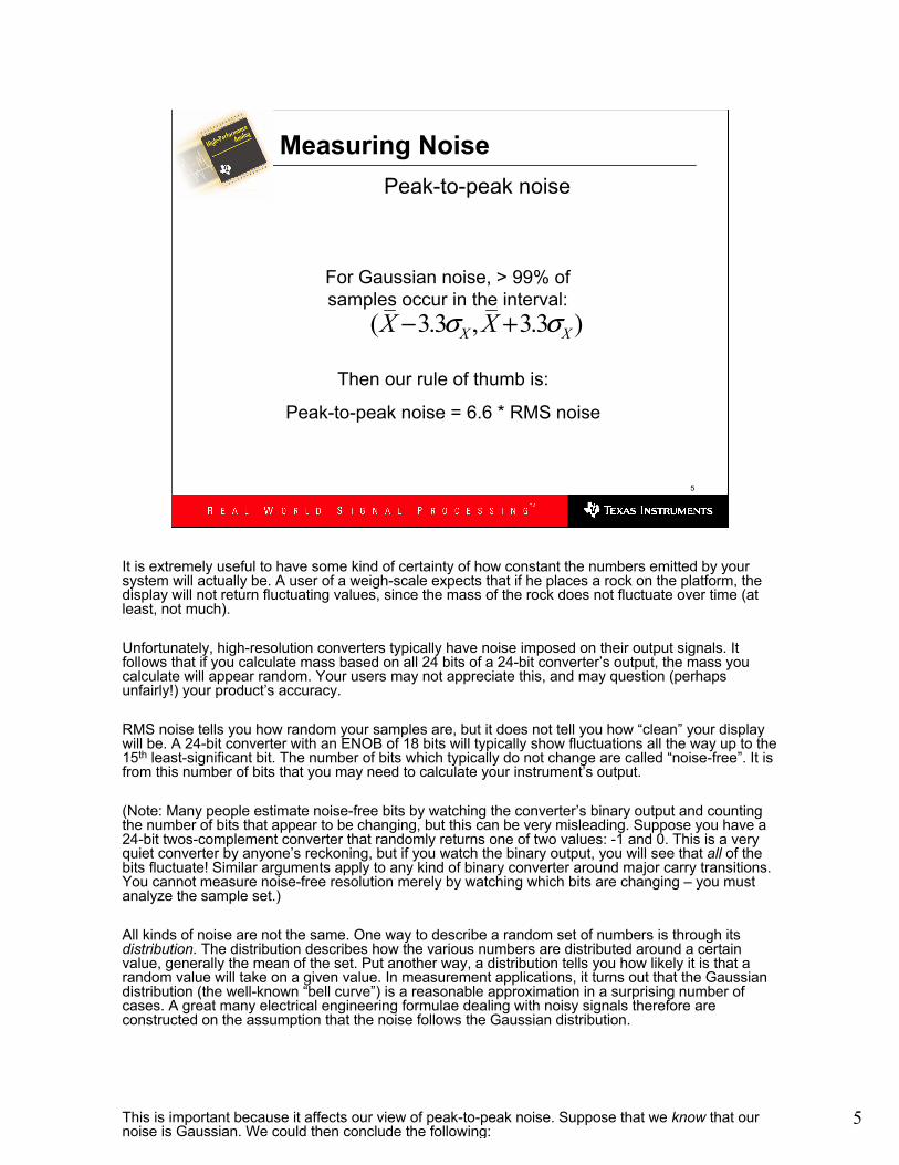
Measuring Noise
Peak-to-peak noise
( 3.3 , 3.3 )X XX Xσ σ− +
For Gaussian noise, > 99% of
samples occur in the interval:
Then our rule of thumb is:
Peak-to-peak noise = 6.6 * RMS noise
It is extremely useful to have some kind of certainty of how constant the numbers emitted by your system will actually be. A user of a weigh-scale expects that if he places a rock on the platform, the display will not return fluctuating values, since the mass of the rock does not fluctuate over time (at least, not much).
Unfortunately, high-resolution converters typically have noise imposed on their output signals. It follows that if you calculate mass based on all 24 bits of a 24-bit converter’s output, the mass you calculate will appear random. Your users may not appreciate this, and may question (perhaps unfairly!) your product’s accuracy.
RMS noise tells you how random your samples are, but it does not tell you how “clean” your display will be. A 24-bit converter with an ENOB of 18 bits will typically show fluctuations all the way up to the 15th least-significant bit. The number of bits which typically do not change are called “noise-free”. It is from this number of bits that you may need to calculate your instrument’s output.
(Note: Many people estimate noise-free bits by watching the converter’s binary output and counting the number of bits that appear to be changing, but this can be very misleading. Suppose you have a 24-bit twos-complement converter that randomly returns one of two values: -1 and 0. This is a very quiet converter by anyone’s reckoning, but if you watch the binary output, you will see that all of the bits fluctuate! Similar arguments apply to any kind of binary converter around major carry transitions. You cannot measure noise-free resolution merely by watching which bits are changing – you must analyze the sample set.)
All kinds of noise are not the same. One way to describe a random set of numbers is through its distribution. The distribution describes how the various numbers are distributed around a certain value, generally the mean of the set. Put another way, a distribution tells you how likely it is that a random value will take on a given value. In measurement applications, it turns out that the Gaussian distribution (the well-known “bell curve”) is a reasonable approximation in a surprising number of cases. A great many electrical engineering formulae dealing with noisy signals therefore are constructed on the assumption that the noise follows the Gaussian distribution.
This is important because it affects our view of peak-to-peak noise. Suppose that we know that our noise is Gaussian. We could then conclude the following:
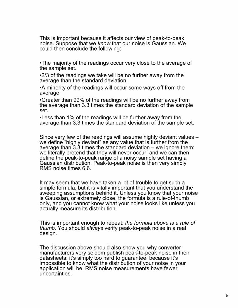
6
This is important because it affects our view of peak-to-peak noise. Suppose that we know that our noise is Gaussian. We could then conclude the following:
•The majority of the readings occur very close to the average of the sample set.
•2/3 of the readings we take will be no further away from the average than the standard deviation.
•A minority of the readings will occur some ways off from the average.
•Greater than 99% of the readings will be no further away from the average than 3.3 times the standard deviation of the sample set.
•Less than 1% of the readings will be further away from the average than 3.3 times the standard deviation of the sample set.
Since very few of the readings will assume highly deviant values –we define “highly deviant” as any value that is further from the average than 3.3 times the standard deviation – we ignore them: we literally pretend that they will never occur, and we can thendefine the peak-to-peak range of a noisy sample set having a Gaussian distribution. Peak-to-peak noise is then very simply RMS noise times 6.6.
It may seem that we have taken a lot of trouble to get such a simple formula, but it is vitally important that you understand the sweeping assumptions behind it. Unless you know that your noise is Gaussian, or extremely close, the formula is a rule-of-thumb only, and you cannot know what your noise looks like unless you actually measure its distribution.
This is important enough to repeat: the formula above is a rule of thumb. You should always verify peak-to-peak noise in a real design.
The discussion above should also show you why converter manufacturers very seldom publish peak-to-peak noise in their datasheets: it’s simply too hard to guarantee, because it’s impossible to know what the distribution of your noise in your application will be. RMS noise measurements have fewer uncertainties.
7
7
Resolution
• Often expressed in counts or decimal
digits
• Internal resolution is calculated from
RMS noise
• Display resolution is calculated from
peak-to-peak noise
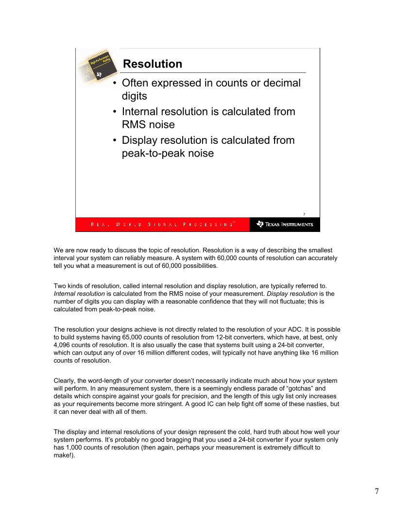
We are now ready to discuss the topic of resolution. Resolution is a way of describing the smallest
interval your system can reliably measure. A system with 60,000 counts of resolution can accurately
tell you what a measurement is out of 60,000 possibilities.
Two kinds of resolution, called internal resolution and display resolution, are typically referred to.
Internal resolution is calculated from the RMS noise of your measurement. Display resolution is the
number of digits you can display with a reasonable confidence that they will not fluctuate; this is
calculated from peak-to-peak noise.
The resolution your designs achieve is not directly related to the resolution of your ADC. It is possible
to build systems having 65,000 counts of resolution from 12-bit converters, which have, at best, only
4,096 counts of resolution. It is also usually the case that systems built using a 24-bit converter,
which can output any of over 16 million different codes, will typically not have anything like 16 million
counts of resolution.
Clearly, the word-length of your converter doesn’t necessarily indicate much about how your system
will perform. In any measurement system, there is a seemingly endless parade of “gotchas” and
details which conspire against your goals for precision, and the length of this ugly list only increases
as your requirements become more stringent. A good IC can help fight off some of these nasties, but
it can never deal with all of them.
The display and internal resolutions of your design represent the cold, hard truth about how well your
system performs. It’s probably no good bragging that you used a 24-bit converter if your system only
has 1,000 counts of resolution (then again, perhaps your measurement is extremely difficult to
make!).
8
8
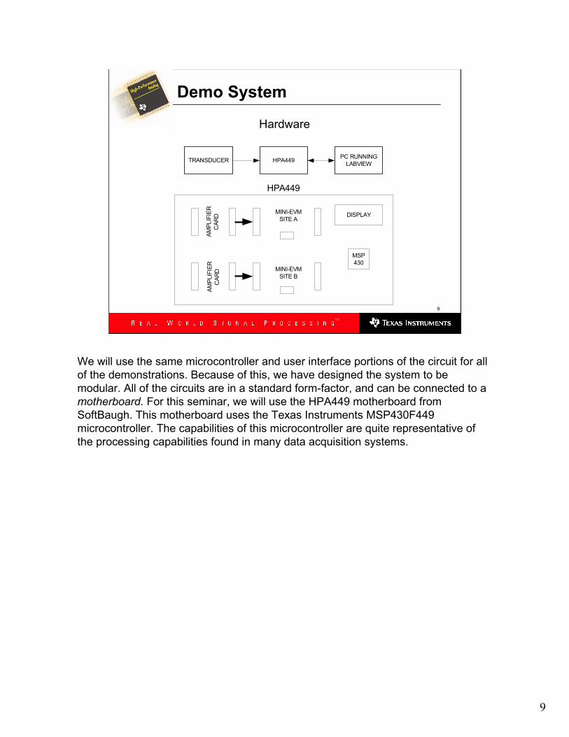
Demo System
TRANSDUCER
(STRAIN GAUGE,
THERMOCOUPLE,
ETC.)
PROTECTION AND
FILTERING
ANALOG-TO-DIGITAL
CONVERTER
INSTRUMENTATION
OR DIFFERENCE
AMPLIFIER
MICROCONTROLLERCOMMUNICATION AND
USER INTERFACE
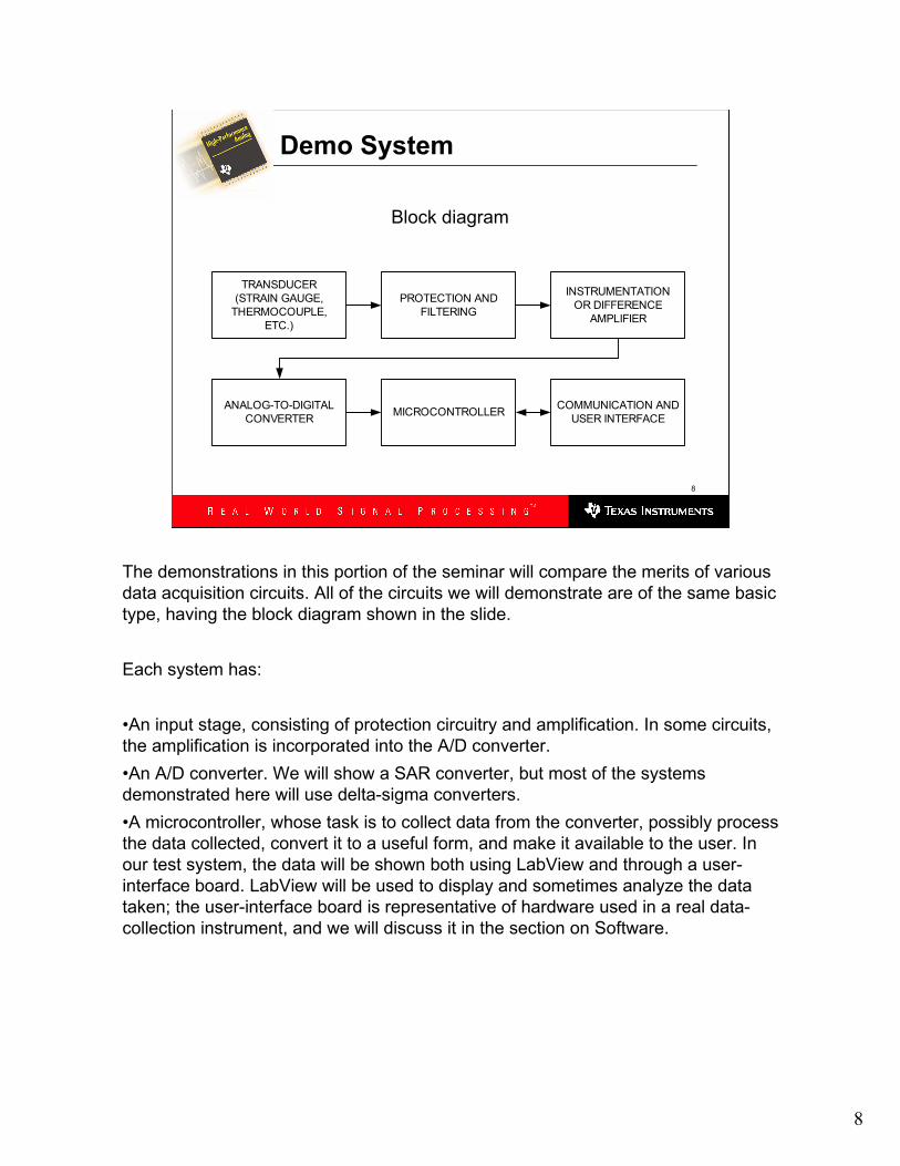
Block diagram
The demonstrations in this portion of the seminar will compare the merits of various
data acquisition circuits. All of the circuits we will demonstrate are of the same basic
type, having the block diagram shown in the slide.
Each system has:
•An input stage, consisting of protection circuitry and amplification. In some circuits,
the amplification is incorporated into the A/D converter.
•An A/D converter. We will show a SAR converter, but most of the systems
demonstrated here will use delta-sigma converters.
•A microcontroller, whose task is to collect data from the converter, possibly process
the data collected, convert it to a useful form, and make it available to the user. In
our test system, the data will be shown both using LabView and through a user-
interface board. LabView will be used to display and sometimes analyze the data
taken; the user-interface board is representative of hardware used in a real data-
collection instrument, and we will discuss it in the section on Software.
9
9
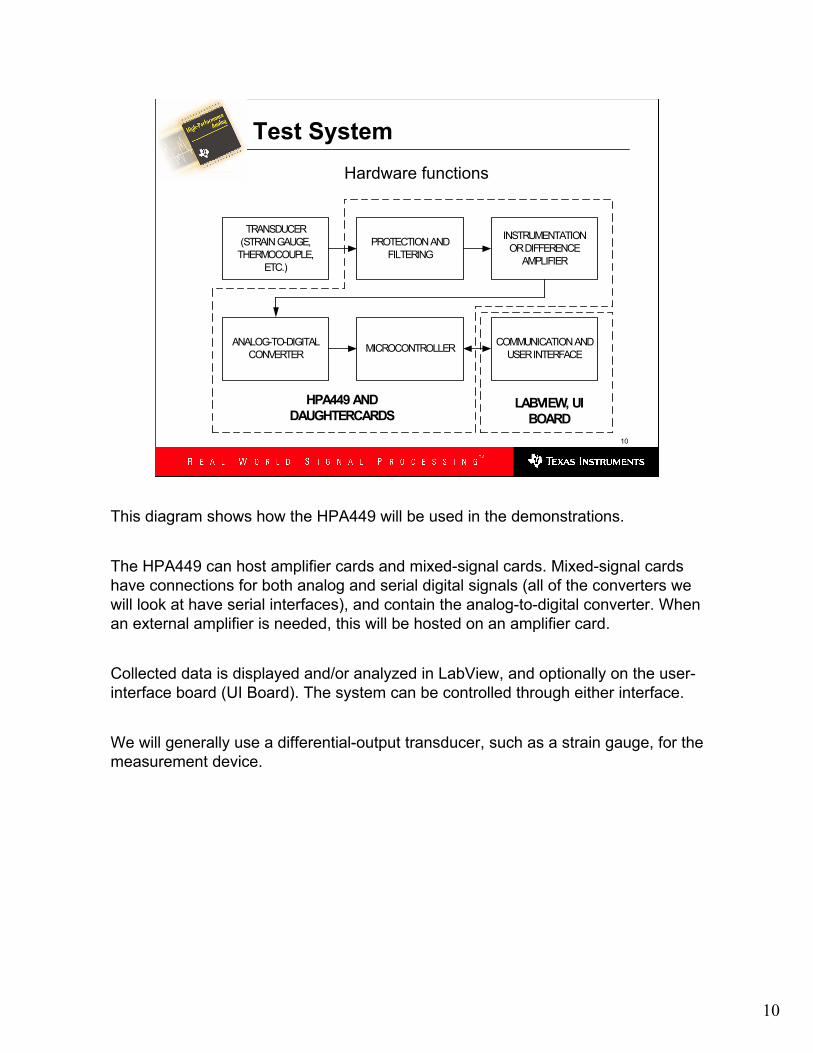
Demo System
TRANSDUCER HPA449PC RUNNING
LABVIEW
DISPLAY
MSP
430MINI-EVM
SITE B
MINI-EVM
SITE A
AM
PLIF
IER
CA
RD
AM
PLIF
IER
CA
RD
HPA449
Hardware
We will use the same microcontroller and user interface portions of the circuit for all
of the demonstrations. Because of this, we have designed the system to be
modular. All of the circuits are in a standard form-factor, and can be connected to a
motherboard. For this seminar, we will use the HPA449 motherboard from
SoftBaugh. This motherboard uses the Texas Instruments MSP430F449
microcontroller. The capabilities of this microcontroller are quite representative of
the processing capabilities found in many data acquisition systems.
10
10
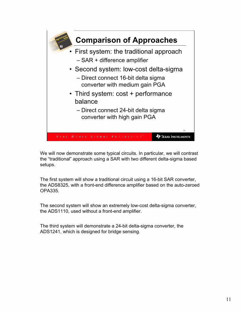
Test System
TRANSDUCER
(STRAIN GAUGE,
THERMOCOUPLE,
ETC.)
PROTECTION AND
FILTERING
ANALOG-TO-DIGITAL
CONVERTER
INSTRUMENTATION
OR DIFFERENCE
AMPLIFIER
MICROCONTROLLERCOMMUNICATION AND
USER INTERFACE
HPA449 AND
DAUGHTERCARDSLABVIEW, UI
BOARD
Hardware functions
This diagram shows how the HPA449 will be used in the demonstrations.
The HPA449 can host amplifier cards and mixed-signal cards. Mixed-signal cards
have connections for both analog and serial digital signals (all of the converters we
will look at have serial interfaces), and contain the analog-to-digital converter. When
an external amplifier is needed, this will be hosted on an amplifier card.
Collected data is displayed and/or analyzed in LabView, and optionally on the user-
interface board (UI Board). The system can be controlled through either interface.
We will generally use a differential-output transducer, such as a strain gauge, for the
measurement device.
11
11
Comparison of Approaches
• First system: the traditional approach
– SAR + difference amplifier
• Second system: low-cost delta-sigma
– Direct connect 16-bit delta sigma
converter with medium gain PGA
• Third system: cost + performance
balance
– Direct connect 24-bit delta sigma
converter with high gain PGA
We will now demonstrate some typical circuits. In particular, we will contrast
the “traditional” approach using a SAR with two different delta-sigma based
setups.
The first system will show a traditional circuit using a 16-bit SAR converter,
the ADS8325, with a front-end difference amplifier based on the auto-zeroed
OPA335.
The second system will show an extremely low-cost delta-sigma converter,
the ADS1110, used without a front-end amplifier.
The third system will demonstrate a 24-bit delta-sigma converter, the
ADS1241, which is designed for bridge sensing.
12
12
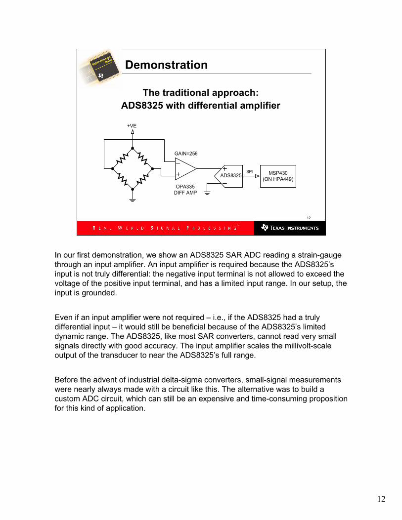
Demonstration
The traditional approach:
ADS8325 with differential amplifier
+VE
GAIN=256
MSP430
(ON HPA449)
SPI
OPA335
DIFF AMP
ADS8325
In our first demonstration, we show an ADS8325 SAR ADC reading a strain-gauge
through an input amplifier. An input amplifier is required because the ADS8325’s
input is not truly differential: the negative input terminal is not allowed to exceed the
voltage of the positive input terminal, and has a limited input range. In our setup, the
input is grounded.
Even if an input amplifier were not required – i.e., if the ADS8325 had a truly
differential input – it would still be beneficial because of the ADS8325’s limited
dynamic range. The ADS8325, like most SAR converters, cannot read very small
signals directly with good accuracy. The input amplifier scales the millivolt-scale
output of the transducer to near the ADS8325’s full range.
Before the advent of industrial delta-sigma converters, small-signal measurements
were nearly always made with a circuit like this. The alternative was to build a
custom ADC circuit, which can still be an expensive and time-consuming proposition
for this kind of application.
13
13
Demonstration
Lowest cost:
ADS1110 with direct connection
+VE
GAIN=8
MSP430
(ON HPA449)
I2CADS1110
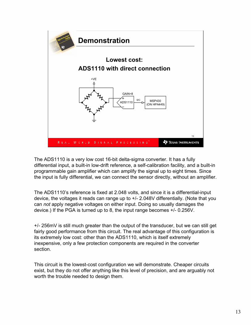
The ADS1110 is a very low cost 16-bit delta-sigma converter. It has a fully
differential input, a built-in low-drift reference, a self-calibration facility, and a built-in
programmable gain amplifier which can amplify the signal up to eight times. Since
the input is fully differential, we can connect the sensor directly, without an amplifier.
The ADS1110’s reference is fixed at 2.048 volts, and since it is a differential-input
device, the voltages it reads can range up to +/- 2.048V differentially. (Note that you
can not apply negative voltages on either input. Doing so usually damages the
device.) If the PGA is turned up to 8, the input range becomes +/- 0.256V.
+/- 256mV is still much greater than the output of the transducer, but we can still get
fairly good performance from this circuit. The real advantage of this configuration is
its extremely low cost: other than the ADS1110, which is itself extremely
inexpensive, only a few protection components are required in the converter
section.
This circuit is the lowest-cost configuration we will demonstrate. Cheaper circuits
exist, but they do not offer anything like this level of precision, and are arguably not
worth the trouble needed to design them.
14
14
Demonstration
High resolution:
ADS1241 with direct connection
+VE
GAIN=128
MSP430
(ON HPA449)
SPI
ADS1241
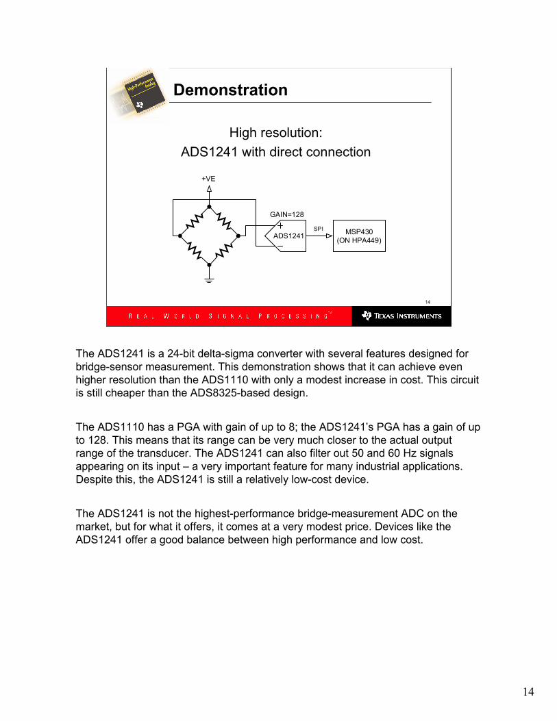
The ADS1241 is a 24-bit delta-sigma converter with several features designed for
bridge-sensor measurement. This demonstration shows that it can achieve even
higher resolution than the ADS1110 with only a modest increase in cost. This circuit
is still cheaper than the ADS8325-based design.
The ADS1110 has a PGA with gain of up to 8; the ADS1241’s PGA has a gain of up
to 128. This means that its range can be very much closer to the actual output
range of the transducer. The ADS1241 can also filter out 50 and 60 Hz signals
appearing on its input – a very important feature for many industrial applications.
Despite this, the ADS1241 is still a relatively low-cost device.
The ADS1241 is not the highest-performance bridge-measurement ADC on the
market, but for what it offers, it comes at a very modest price. Devices like the
ADS1241 offer a good balance between high performance and low cost.
15
15
Comparison
Fairly low
Lowest
Highest
Cost
HighADS1241Delta-sigmaIntegrated
DecentADS1110Delta-sigmaLow cost
DecentADS8325
+ OPA335
SAR +
amplifier
Traditional
PerformanceDeviceTechnologyApproach
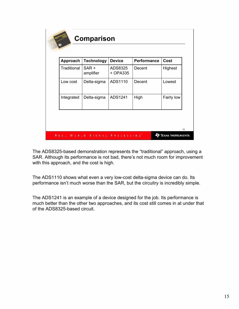
The ADS8325-based demonstration represents the “traditional” approach, using a
SAR. Although its performance is not bad, there’s not much room for improvement
with this approach, and the cost is high.
The ADS1110 shows what even a very low-cost delta-sigma device can do. Its
performance isn’t much worse than the SAR, but the circuitry is incredibly simple.
The ADS1241 is an example of a device designed for the job. Its performance is
much better than the other two approaches, and its cost still comes in at under that
of the ADS8325-based circuit.
16
16
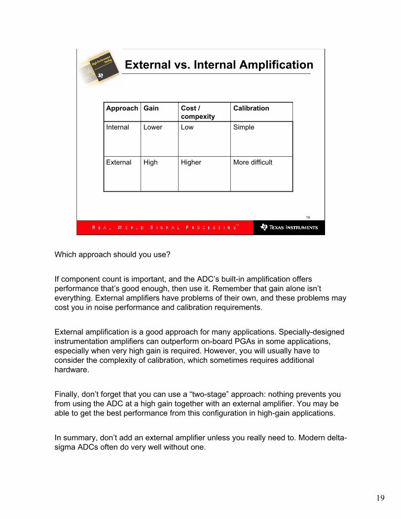
External vs. Internal Amplification
• External amplifiers
– Usually required when the ADC has no
on-board amplifier
– Can be expensive
• Internal amplifiers
– Available on many delta-sigma ADCs
and some SARs
We will now compare two amplification approaches: external and internal.
Many designers are in the habit of placing an amplifier in front of ADCs,
whether or not the ADC has on-board gain. This is not always the best
approach. Many high-resolution delta-sigma ADCs can actually perform
better without an external amplifier. Eliminating it not only can improve
performance, but save on board space, parts count, and cost.
The next two demonstrations will also demonstrate one of TI’s highest-
performance delta-sigma converters, the ADS1256. This device (and its
companion, the single-channel ADS1255) offers both extremely low noise at
low data rates and good performance at higher data rates.
17
17
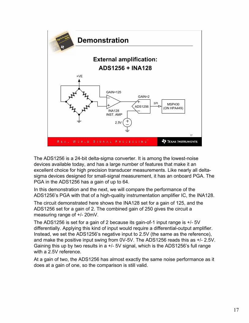
Demonstration
External amplification:
ADS1256 + INA128
+VE
GAIN=125
MSP430
(ON HPA449)
SPI
INA128
INST. AMP
ADS1256
2.5V
GAIN=2
The ADS1256 is a 24-bit delta-sigma converter. It is among the lowest-noise
devices available today, and has a large number of features that make it an
excellent choice for high precision transducer measurements. Like nearly all delta-
sigma devices designed for small-signal measurement, it has an onboard PGA. The
PGA in the ADS1256 has a gain of up to 64.
In this demonstration and the next, we will compare the performance of the
ADS1256’s PGA with that of a high-quality instrumentation amplifier IC, the INA128.
The circuit demonstrated here shows the INA128 set for a gain of 125, and the
ADS1256 set for a gain of 2. The combined gain of 250 gives the circuit a
measuring range of +/- 20mV.
The ADS1256 is set for a gain of 2 because its gain-of-1 input range is +/- 5V
differentially. Applying this kind of input would require a differential-output amplifier.
Instead, we set the ADS1256’s negative input to 2.5V (the same as the reference),
and make the positive input swing from 0V-5V. The ADS1256 reads this as +/- 2.5V.
Gaining this up by two results in a +/- 5V signal, which is the ADS1256’s full range
with a 2.5V reference.
At a gain of two, the ADS1256 has almost exactly the same noise performance as it
does at a gain of one, so the comparison is still valid.
18
18
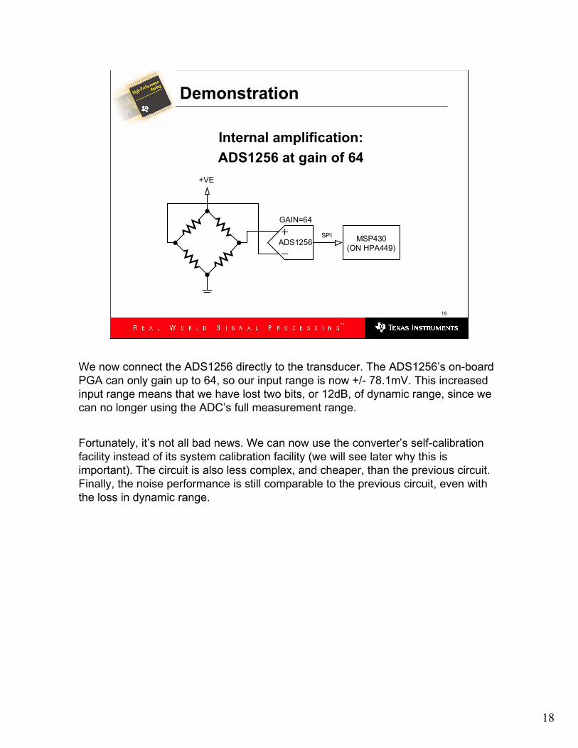
Demonstration
Internal amplification:
ADS1256 at gain of 64
+VE
GAIN=64
MSP430
(ON HPA449)
SPI
ADS1256
We now connect the ADS1256 directly to the transducer. The ADS1256’s on-board
PGA can only gain up to 64, so our input range is now +/- 78.1mV. This increased
input range means that we have lost two bits, or 12dB, of dynamic range, since we
can no longer using the ADC’s full measurement range.
Fortunately, it’s not all bad news. We can now use the converter’s self-calibration
facility instead of its system calibration facility (we will see later why this is
important). The circuit is also less complex, and cheaper, than the previous circuit.
Finally, the noise performance is still comparable to the previous circuit, even with
the loss in dynamic range.
19
19
External vs. Internal Amplification
More difficultHigherHighExternal
SimpleLowLowerInternal
CalibrationCost /
compexity
GainApproach
Which approach should you use?
If component count is important, and the ADC’s built-in amplification offers
performance that’s good enough, then use it. Remember that gain alone isn’t
everything. External amplifiers have problems of their own, and these problems may
cost you in noise performance and calibration requirements.
External amplification is a good approach for many applications. Specially-designed
instrumentation amplifiers can outperform on-board PGAs in some applications,
especially when very high gain is required. However, you will usually have to
consider the complexity of calibration, which sometimes requires additional
hardware.
Finally, don’t forget that you can use a “two-stage” approach: nothing prevents you
from using the ADC at a high gain together with an external amplifier. You may be
able to get the best performance from this configuration in high-gain applications.
In summary, don’t add an external amplifier unless you really need to. Modern delta-
sigma ADCs often do very well without one.
20
20
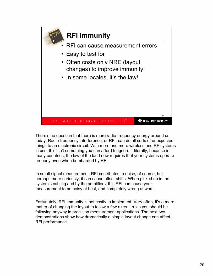
RFI Immunity
• RFI can cause measurement errors
• Easy to test for
• Often costs only NRE (layout
changes) to improve immunity
• In some locales, it’s the law!
There’s no question that there is more radio-frequency energy around us
today. Radio-frequency interference, or RFI, can do all sorts of unexpected
things to an electronic circuit. With more and more wireless and RF systems
in use, this isn’t something you can afford to ignore – literally, because in
many countries, the law of the land now requires that your systems operate
properly even when bombarded by RFI.
In small-signal measurement, RFI contributes to noise, of course, but
perhaps more seriously, it can cause offset shifts. When picked up in the
system’s cabling and by the amplifiers, this RFI can cause your
measurement to be noisy at best, and completely wrong at worst.
Fortunately, RFI immunity is not costly to implement. Very often, it’s a mere
matter of changing the layout to follow a few rules – rules you should be
following anyway in precision measurement applications. The next two
demonstrations show how dramatically a simple layout change can affect
RFI performance.
21
21
RFI Immunity
Time
Vout
AmplifierSensor
RF Source
VosVos Shift!Shift!Result:
Conducted
Radiated
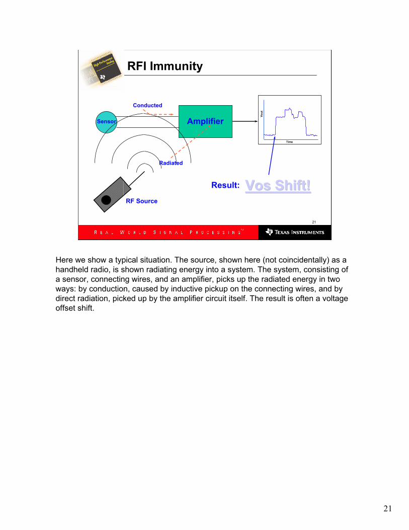
Here we show a typical situation. The source, shown here (not coincidentally) as a
handheld radio, is shown radiating energy into a system. The system, consisting of
a sensor, connecting wires, and an amplifier, picks up the radiated energy in two
ways: by conduction, caused by inductive pickup on the connecting wires, and by
direct radiation, picked up by the amplifier circuit itself. The result is often a voltage
offset shift.
22
22
Demonstration
ADS1256 + OPA335: poor layout
+VE
GAIN=125
MSP430
(ON HPA449)
SPI
OPA335
DIFF AMP
ADS1256
2.5V
GAIN=2
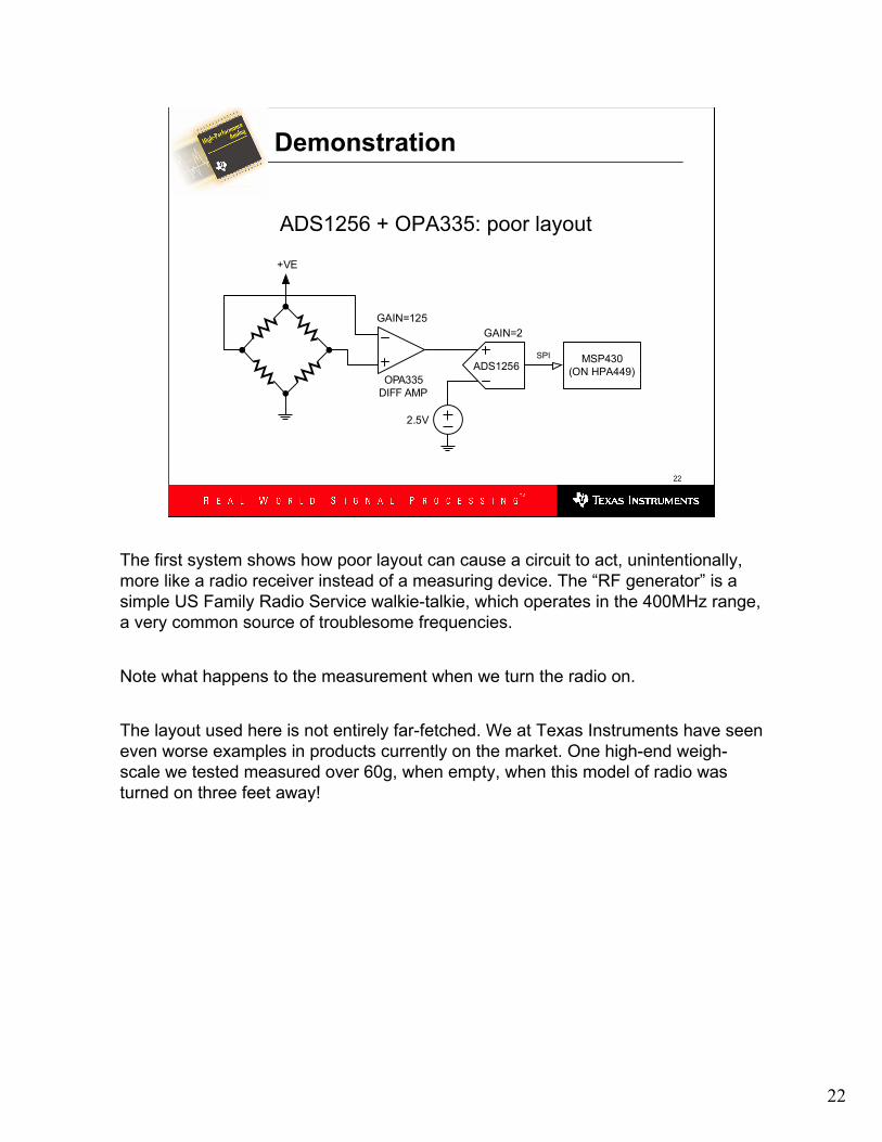
The first system shows how poor layout can cause a circuit to act, unintentionally,
more like a radio receiver instead of a measuring device. The “RF generator” is a
simple US Family Radio Service walkie-talkie, which operates in the 400MHz range,
a very common source of troublesome frequencies.
Note what happens to the measurement when we turn the radio on.
The layout used here is not entirely far-fetched. We at Texas Instruments have seen
even worse examples in products currently on the market. One high-end weigh-
scale we tested measured over 60g, when empty, when this model of radio was
turned on three feet away!
23
23
Demonstration
ADS1256 + OPA335: good layout
+VE
GAIN=125
MSP430
(ON HPA449)
SPI
OPA335
DIFF AMP
ADS1256
2.5V
GAIN=2
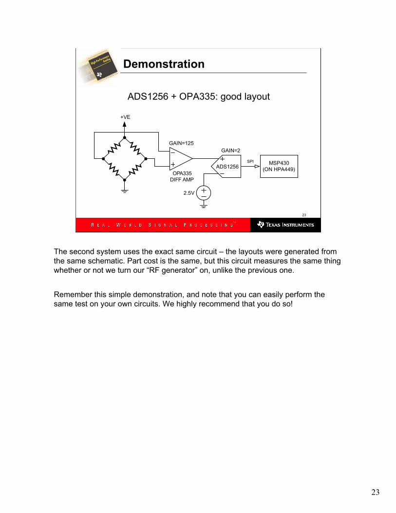
The second system uses the exact same circuit – the layouts were generated from
the same schematic. Part cost is the same, but this circuit measures the same thing
whether or not we turn our “RF generator” on, unlike the previous one.
Remember this simple demonstration, and note that you can easily perform the
same test on your own circuits. We highly recommend that you do so!
24
24
Temperature Compensation
• Many sensors must be temperature
compensated
• Nearly all components act like
thermometers!
• Use temperature sensors and
firmware to compensate
– Examples: thermistors, on-board temp
diodes, IC temp sensor devices
Unless you are measuring temperature, you will likely want to perform some kind of temperature compensation in your circuit.
Most sensors, whether intentionally or not, act as thermometers. A strain-gauge drifts with temperature due to a number of effects: the resistance strips have a temperature characteristic, and self-heating caused by excitation can cause the strips to expand, which in turn causes a strain on the gauge, which affects the measurement.
Another source of temperature drift is, of course, the components in your circuit. Resistors, capacitors, and especially anything made of silicon – all are really thermometers, whether you like it or not.
Fortunately, compensating for temperature is not expensive, especially if you are using a microcontroller which can calculate the necessary corrections mathematically. Also, most good IC designers are well aware of temperature effects on circuits – a remarkable amount of their time is spent compensating for them.
To compensate for temperature, you have to know what the temperature is. In temperature compensation, it is usually not necessary to have an extremely accurate measurement of temperature. In some circuits, all that is needed is information about whether the temperature has recently changed by an appreciable amount.
Many kinds of temperature sensors are available. If you have extra channels on your ADC, a simple thermistor can be used to measure the ambient temperature. Some ADCs have temperature-measurement diodes built in to them, as do some microcontrollers – the MSP430F449 used in our demonstrations has one. You can also purchase temperature-measurement ICs, which are precalibrated and ready to use. The TMP100 is an example, and we have included one on our amplifier card.
25
25
Demonstration
Temperature compensation
I2C
+VE
GAIN=64
MSP430
(ON HPA449)
SPI
ADS1256
TMP100
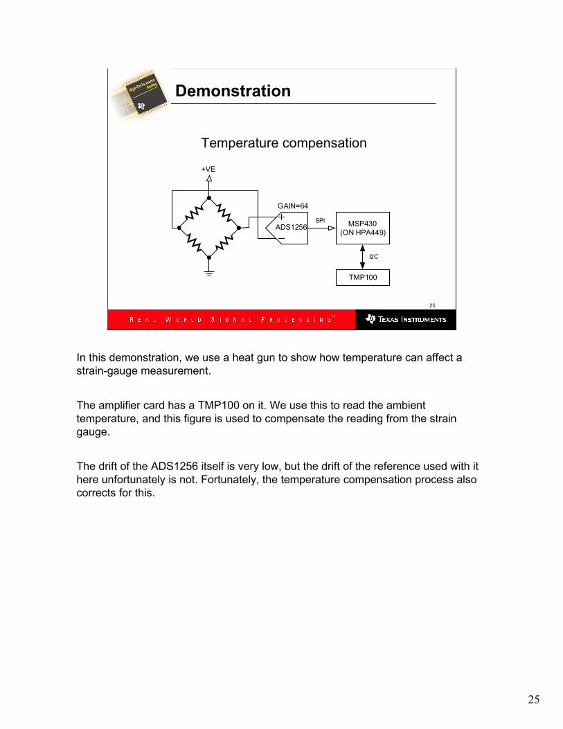
In this demonstration, we use a heat gun to show how temperature can affect a
strain-gauge measurement.
The amplifier card has a TMP100 on it. We use this to read the ambient
temperature, and this figure is used to compensate the reading from the strain
gauge.
The drift of the ADS1256 itself is very low, but the drift of the reference used with it
here unfortunately is not. Fortunately, the temperature compensation process also
corrects for this.
26
26
Ratiometric Measurement
in in
ref E
strainin
E max
strain E
E max
code 2 2
code 2
N N
N
V V
V V
FV
kV F
F V
kV F
= =
=
=strain
max
code 2NF
kF=
ADC
+VE
VREF
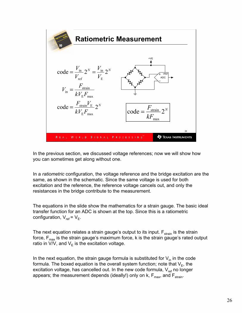
In the previous section, we discussed voltage references; now we will show how
you can sometimes get along without one.
In a ratiometric configuration, the voltage reference and the bridge excitation are the
same, as shown in the schematic. Since the same voltage is used for both
excitation and the reference, the reference voltage cancels out, and only the
resistances in the bridge contribute to the measurement.
The equations in the slide show the mathematics for a strain gauge. The basic ideal
transfer function for an ADC is shown at the top. Since this is a ratiometric
configuration, Vref = VE.
The next equation relates a strain gauge’s output to its input. Fstrain is the strain
force, Fmax is the strain gauge’s maximum force, k is the strain gauge’s rated output
ratio in V/V, and VE is the excitation voltage.
In the next equation, the strain gauge formula is substituted for Vin in the code
formula. The boxed equation is the overall system function; note that VE, the
excitation voltage, has cancelled out. In the new code formula, Vref no longer
appears; the measurement depends (ideally!) only on k, Fmax, and Fstrain.
27
27
Demonstration
ADS1256 in a ratiometric configuration
ADS1256
+VE
VREF+
MSP430
(ON HPA449)VREF-
SPI
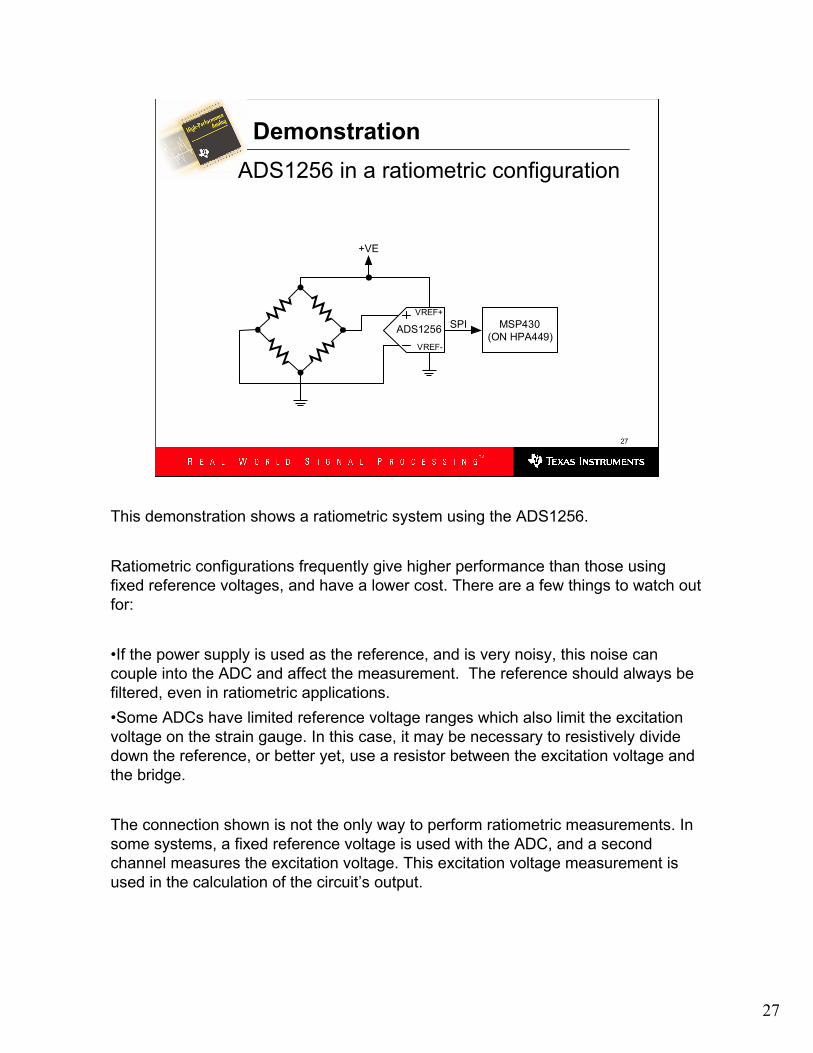
This demonstration shows a ratiometric system using the ADS1256.
Ratiometric configurations frequently give higher performance than those using
fixed reference voltages, and have a lower cost. There are a few things to watch out
for:
•If the power supply is used as the reference, and is very noisy, this noise can
couple into the ADC and affect the measurement. The reference should always be
filtered, even in ratiometric applications.
•Some ADCs have limited reference voltage ranges which also limit the excitation
voltage on the strain gauge. In this case, it may be necessary to resistively divide
down the reference, or better yet, use a resistor between the excitation voltage and
the bridge.
The connection shown is not the only way to perform ratiometric measurements. In
some systems, a fixed reference voltage is used with the ADC, and a second
channel measures the excitation voltage. This excitation voltage measurement is
used in the calculation of the circuit’s output.
28
28
Firmware Design
• I/O: the main task
• Output is easy
• Input is hard
In a data-acquisition system, the main task of the firmware is input and output. This
statement may seem obvious, but it has important implications for the design of
data-acquisition firmware.
Many people focus on the signal-processing functions of firmware. These are
certainly important, but they do not affect the overall design of the firmware nearly
as much as the input and output structure does.
A computer, as typically programmed, is a naturally proactive device. The vast
majority of programming languages and computer designs see the computer as a
tool for executing algorithms. Almost all programming languages are essentially
ways to give the computer a list of things to do. This makes the output functions
easy: in most programming languages, when you want to output data, you simply do
so. In this sense, output is not much different from mathematical processing.
Unfortunately, input often is not well provided for, and this is partly because input is
hard. When you are generating data, you have complete control; you can ensure
that you generate the right data. When you must process incoming data, however,
there is much more room for error. You must be prepared to accept and deal
properly with anything that can enter your system, and you must do it when the
input arrives. This is a fundamentally more difficult problem than generating output.
29
29
Data Input Strategies
• Polling
• Interrupts
• Blocking
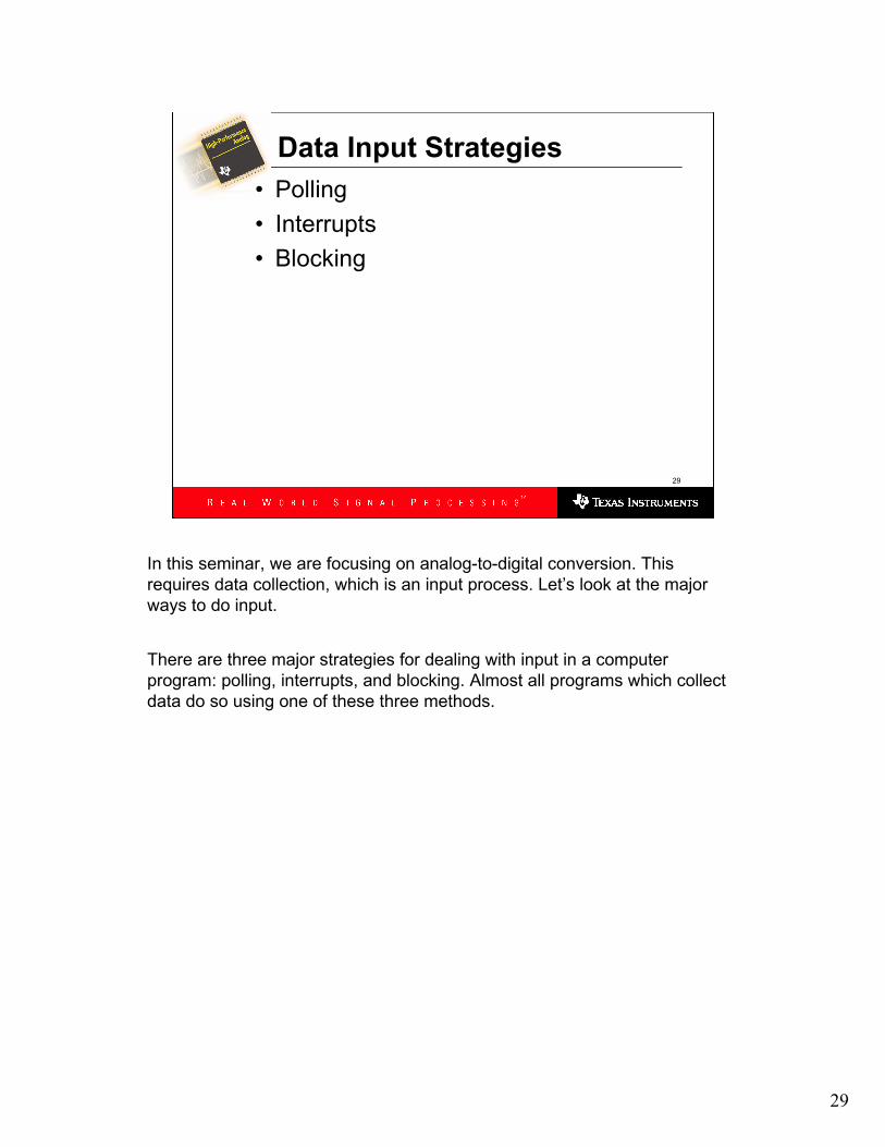
In this seminar, we are focusing on analog-to-digital conversion. This
requires data collection, which is an input process. Let’s look at the major
ways to do input.
There are three major strategies for dealing with input in a computer
program: polling, interrupts, and blocking. Almost all programs which collect
data do so using one of these three methods.
30
30
Data Input Strategies
A polled system
START
CHECK FOR
DATA
DATA
PRESENT?
PROCESS
DATA
DELAY
RETRIEVE
DATA
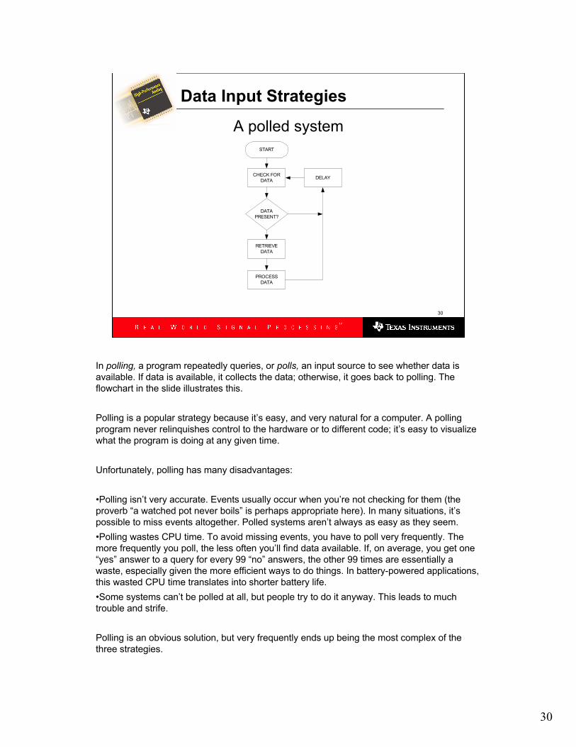
In polling, a program repeatedly queries, or polls, an input source to see whether data is
available. If data is available, it collects the data; otherwise, it goes back to polling. The
flowchart in the slide illustrates this.
Polling is a popular strategy because it’s easy, and very natural for a computer. A polling
program never relinquishes control to the hardware or to different code; it’s easy to visualize
what the program is doing at any given time.
Unfortunately, polling has many disadvantages:
•Polling isn’t very accurate. Events usually occur when you’re not checking for them (the
proverb “a watched pot never boils” is perhaps appropriate here). In many situations, it’s
possible to miss events altogether. Polled systems aren’t always as easy as they seem.
•Polling wastes CPU time. To avoid missing events, you have to poll very frequently. The
more frequently you poll, the less often you’ll find data available. If, on average, you get one
“yes” answer to a query for every 99 “no” answers, the other 99 times are essentially a
waste, especially given the more efficient ways to do things. In battery-powered applications,
this wasted CPU time translates into shorter battery life.
•Some systems can’t be polled at all, but people try to do it anyway. This leads to much
trouble and strife.
Polling is an obvious solution, but very frequently ends up being the most complex of the
three strategies.
31
31
Data Input Strategies
An interrupt-triggered system
END INTERRUPT
RETRIEVE
DATA
PROCESS
DATA
INTERRUPT
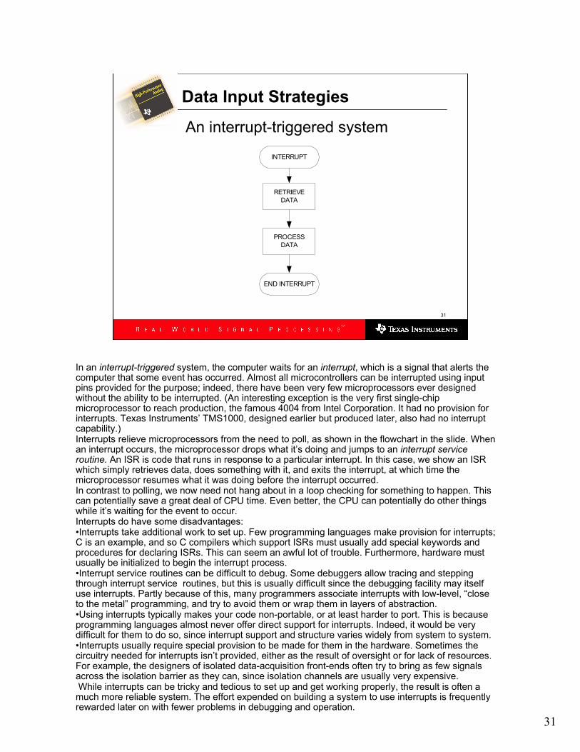
In an interrupt-triggered system, the computer waits for an interrupt, which is a signal that alerts the computer that some event has occurred. Almost all microcontrollers can be interrupted using input pins provided for the purpose; indeed, there have been very few microprocessors ever designed without the ability to be interrupted. (An interesting exception is the very first single-chip microprocessor to reach production, the famous 4004 from Intel Corporation. It had no provision for interrupts. Texas Instruments’ TMS1000, designed earlier but produced later, also had no interrupt capability.)Interrupts relieve microprocessors from the need to poll, as shown in the flowchart in the slide. When an interrupt occurs, the microprocessor drops what it’s doing and jumps to an interrupt service routine. An ISR is code that runs in response to a particular interrupt. In this case, we show an ISR which simply retrieves data, does something with it, and exits the interrupt, at which time the microprocessor resumes what it was doing before the interrupt occurred.In contrast to polling, we now need not hang about in a loop checking for something to happen. This can potentially save a great deal of CPU time. Even better, the CPU can potentially do other things while it’s waiting for the event to occur.Interrupts do have some disadvantages:•Interrupts take additional work to set up. Few programming languages make provision for interrupts; C is an example, and so C compilers which support ISRs must usually add special keywords and procedures for declaring ISRs. This can seem an awful lot of trouble. Furthermore, hardware must usually be initialized to begin the interrupt process.•Interrupt service routines can be difficult to debug. Some debuggers allow tracing and stepping through interrupt service routines, but this is usually difficult since the debugging facility may itself use interrupts. Partly because of this, many programmers associate interrupts with low-level, “close to the metal” programming, and try to avoid them or wrap them in layers of abstraction.•Using interrupts typically makes your code non-portable, or at least harder to port. This is because programming languages almost never offer direct support for interrupts. Indeed, it would be very difficult for them to do so, since interrupt support and structure varies widely from system to system.•Interrupts usually require special provision to be made for them in the hardware. Sometimes the circuitry needed for interrupts isn’t provided, either as the result of oversight or for lack of resources. For example, the designers of isolated data-acquisition front-ends often try to bring as few signals across the isolation barrier as they can, since isolation channels are usually very expensive.While interrupts can be tricky and tedious to set up and get working properly, the result is often a much more reliable system. The effort expended on building a system to use interrupts is frequently rewarded later on with fewer problems in debugging and operation.
32
32
Data Input Strategies
A blocking system
START
WAIT FOR
DATA (BLOCK)
RETRIEVE
DATA
PROCESS
DATA
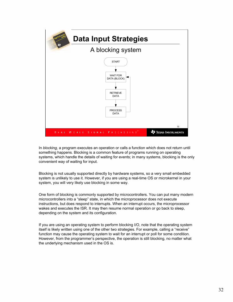
In blocking, a program executes an operation or calls a function which does not return until
something happens. Blocking is a common feature of programs running on operating
systems, which handle the details of waiting for events; in many systems, blocking is the only
convenient way of waiting for input.
Blocking is not usually supported directly by hardware systems, so a very small embedded
system is unlikely to use it. However, if you are using a real-time OS or microkernel in your
system, you will very likely use blocking in some way.
One form of blocking is commonly supported by microcontrollers. You can put many modern
microcontrollers into a “sleep” state, in which the microprocessor does not execute
instructions, but does respond to interrupts. When an interrupt occurs, the microprocessor
wakes and executes the ISR. It may then resume normal operation or go back to sleep,
depending on the system and its configuration.
If you are using an operating system to perform blocking I/O, note that the operating system
itself is likely written using one of the other two strategies. For example, calling a “receive”
function may cause the operating system to wait for an interrupt or poll for some condition.
However, from the programmer’s perspective, the operation is still blocking, no matter what
the underlying mechanism used in the OS is.
33
33
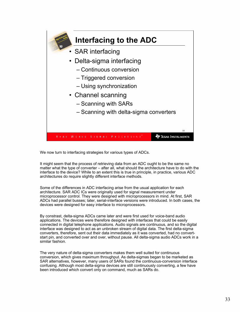
Interfacing to the ADC
• SAR interfacing
• Delta-sigma interfacing
– Continuous conversion
– Triggered conversion
– Using synchronization
• Channel scanning
– Scanning with SARs
– Scanning with delta-sigma converters
We now turn to interfacing strategies for various types of ADCs.
It might seem that the process of retrieving data from an ADC ought to be the same no matter what the type of converter – after all, what should the architecture have to do with the interface to the device? While to an extent this is true in principle, in practice, various ADC architectures do require slightly different interface methods.
Some of the differences in ADC interfacing arise from the usual application for each architecture. SAR ADC ICs were originally used for signal measurement under microprocessor control. They were designed with microprocessors in mind. At first, SAR ADCs had parallel busses; later, serial-interface versions were introduced. In both cases, the devices were designed for easy interface to microprocessors.
By constrast, delta-sigma ADCs came later and were first used for voice-band audio applications. The devices were therefore designed with interfaces that could be easily connected in digital telephone applications. Audio signals are continuous, and so the digital interface was designed to act as an unbroken stream of digital data. The first delta-sigma converters, therefore, sent out their data immediately as it was converted, had no convert-start pin, and converted over and over, without pause. All delta-sigma audio ADCs work in a similar fashion.
The very nature of delta-sigma converters makes them well suited for continuous conversion, which gives maximum throughput. As delta-sigmas began to be marketed as SAR alternatives, however, many users of SARs found the continuous-conversion interface confusing. Although most delta-sigma devices are still continuously converting, a few have been introduced which convert only on command, much as SARs do.
34
34
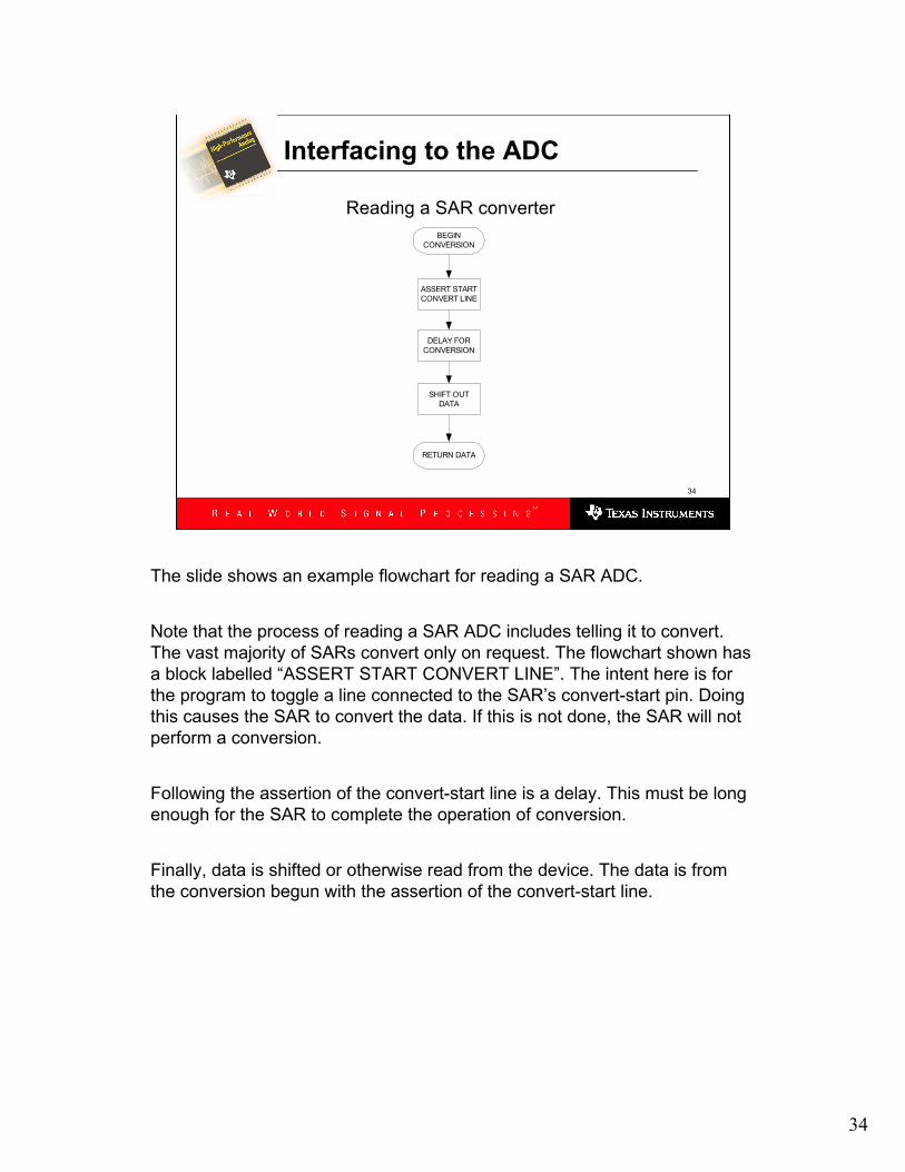
Interfacing to the ADC
Reading a SAR converter
BEGIN
CONVERSION
ASSERT START
CONVERT LINE
DELAY FOR
CONVERSION
SHIFT OUT
DATA
RETURN DATA
The slide shows an example flowchart for reading a SAR ADC.
Note that the process of reading a SAR ADC includes telling it to convert.
The vast majority of SARs convert only on request. The flowchart shown has
a block labelled “ASSERT START CONVERT LINE”. The intent here is for
the program to toggle a line connected to the SAR’s convert-start pin. Doing
this causes the SAR to convert the data. If this is not done, the SAR will not
perform a conversion.
Following the assertion of the convert-start line is a delay. This must be long
enough for the SAR to complete the operation of conversion.
Finally, data is shifted or otherwise read from the device. The data is from
the conversion begun with the assertion of the convert-start line.
35
35
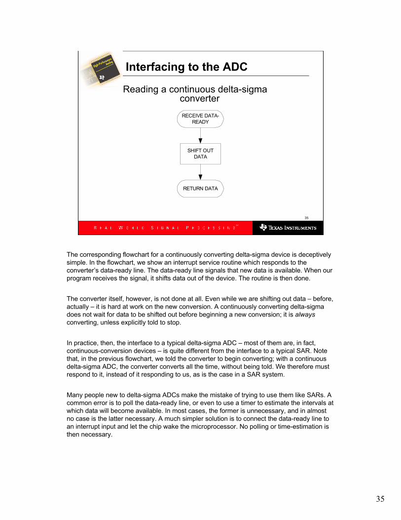
Interfacing to the ADC
Reading a continuous delta-sigma converter
RECEIVE DATA-
READY
SHIFT OUT
DATA
RETURN DATA
The corresponding flowchart for a continuously converting delta-sigma device is deceptively
simple. In the flowchart, we show an interrupt service routine which responds to the
converter’s data-ready line. The data-ready line signals that new data is available. When our
program receives the signal, it shifts data out of the device. The routine is then done.
The converter itself, however, is not done at all. Even while we are shifting out data – before,
actually – it is hard at work on the new conversion. A continuously converting delta-sigma
does not wait for data to be shifted out before beginning a new conversion; it is always
converting, unless explicitly told to stop.
In practice, then, the interface to a typical delta-sigma ADC – most of them are, in fact,
continuous-conversion devices – is quite different from the interface to a typical SAR. Note
that, in the previous flowchart, we told the converter to begin converting; with a continuous
delta-sigma ADC, the converter converts all the time, without being told. We therefore must
respond to it, instead of it responding to us, as is the case in a SAR system.
Many people new to delta-sigma ADCs make the mistake of trying to use them like SARs. A
common error is to poll the data-ready line, or even to use a timer to estimate the intervals at
which data will become available. In most cases, the former is unnecessary, and in almost
no case is the latter necessary. A much simpler solution is to connect the data-ready line to
an interrupt input and let the chip wake the microprocessor. No polling or time-estimation is
then necessary.
36
36
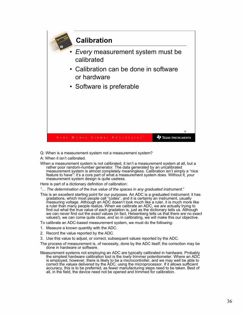
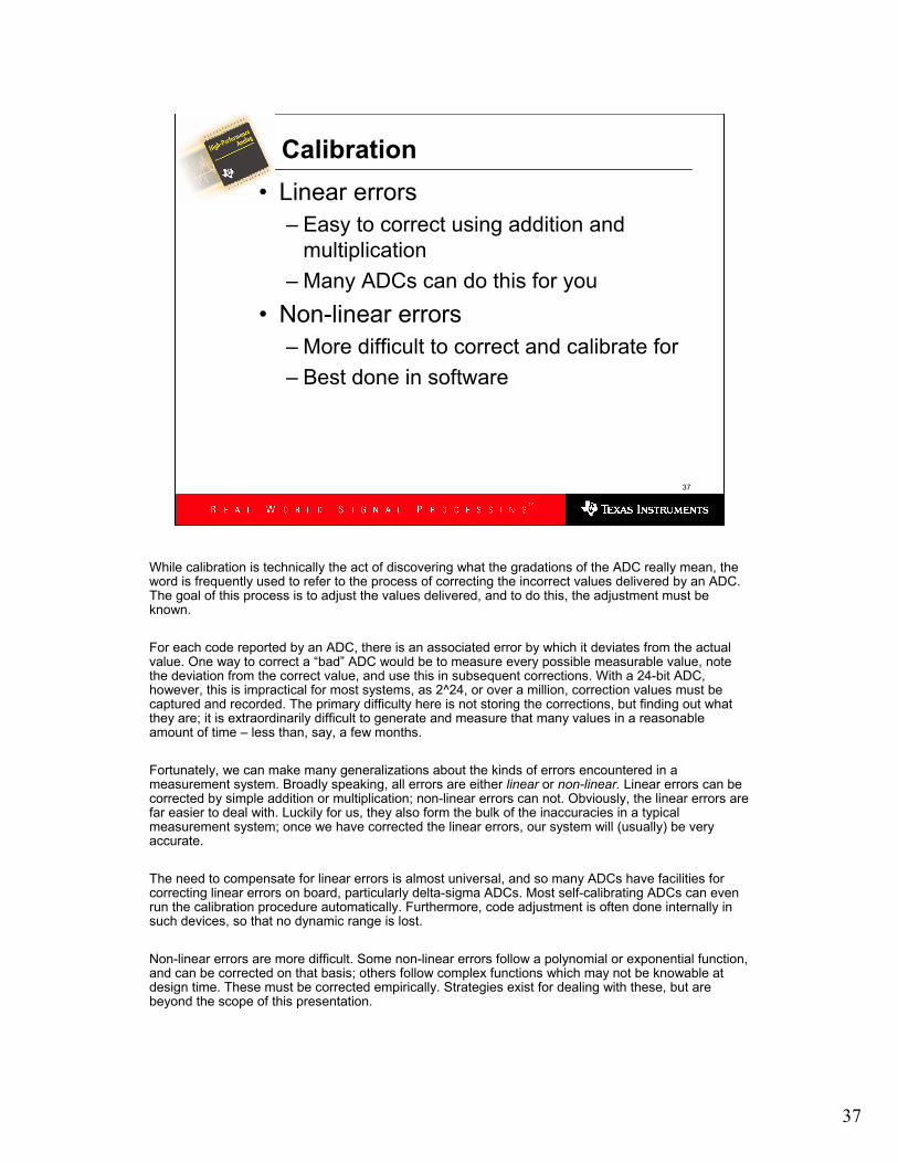
Calibration
• Every measurement system must be
calibrated
• Calibration can be done in software
or hardware
• Software is preferable
Q: When is a measurement system not a measurement system?
A: When it isn’t calibrated.
When a measurement system is not calibrated, it isn’t a measurement system at all, but a rather poor random-number generator. The data generated by an uncalibratedmeasurement system is almost completely meaningless. Calibration isn’t simply a “nice feature to have”: it’s a core part of what a measurement system does. Without it, your measurement system design is quite useless.
Here is part of a dictionary definition of calibration:
”… The determination of the true value of the spaces in any graduated instrument.”
This is an excellent starting point for our purposes. An ADC is a graduated instrument: it has gradations, which most people call “codes”, and it is certainly an instrument, usually measuring voltage. Although an ADC doesn’t look much like a ruler, it is much more like a ruler than many people realize. When we calibrate an ADC, we are actually trying to find out what the true value of each gradation is, just as the dictionary tells us. Although we can never find out the exact values (in fact, Heisenberg tells us that there are no exact values!), we can come quite close, and so in calibrating, we will make this our objective.
To calibrate an ADC-based measurement system, we must do the following:
1. Measure a known quantity with the ADC.
2. Record the value reported by the ADC.
3. Use this value to adjust, or correct, subsequent values reported by the ADC.
The process of measurement is, of necessity, done by the ADC itself; the correction may be done in hardware or software.
Measurement systems not employing an ADC are typically calibrated in hardware. Probably the simplest hardware calibration tool is the lowly trimmer potentiometer. Where an ADC is employed, however, there is likely to be a microcontroller, and we may well be able to correct the values delivered by the ADC, using the microprocessor. If it allows sufficient accuracy, this is to be preferred, as fewer manufacturing steps need to be taken. Best of all, in the field, the device need not be opened and trimmed for calibration.
37
37
Calibration
• Linear errors
– Easy to correct using addition and
multiplication
– Many ADCs can do this for you
• Non-linear errors
– More difficult to correct and calibrate for
– Best done in software
While calibration is technically the act of discovering what the gradations of the ADC really mean, the word is frequently used to refer to the process of correcting the incorrect values delivered by an ADC. The goal of this process is to adjust the values delivered, and to do this, the adjustment must be known.
For each code reported by an ADC, there is an associated error by which it deviates from the actual value. One way to correct a “bad” ADC would be to measure every possible measurable value, note the deviation from the correct value, and use this in subsequent corrections. With a 24-bit ADC, however, this is impractical for most systems, as 2^24, or over a million, correction values must be captured and recorded. The primary difficulty here is not storing the corrections, but finding out what they are; it is extraordinarily difficult to generate and measure that many values in a reasonable amount of time – less than, say, a few months.
Fortunately, we can make many generalizations about the kinds of errors encountered in a measurement system. Broadly speaking, all errors are either linear or non-linear. Linear errors can be corrected by simple addition or multiplication; non-linear errors can not. Obviously, the linear errors are far easier to deal with. Luckily for us, they also form the bulk of the inaccuracies in a typical measurement system; once we have corrected the linear errors, our system will (usually) be very accurate.
The need to compensate for linear errors is almost universal, and so many ADCs have facilities for correcting linear errors on board, particularly delta-sigma ADCs. Most self-calibrating ADCs can even run the calibration procedure automatically. Furthermore, code adjustment is often done internally in such devices, so that no dynamic range is lost.
Non-linear errors are more difficult. Some non-linear errors follow a polynomial or exponential function, and can be corrected on that basis; others follow complex functions which may not be knowable at design time. These must be corrected empirically. Strategies exist for dealing with these, but are beyond the scope of this presentation.
38
38
Calibration
1
0.5
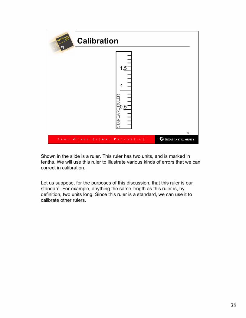
1.5
Shown in the slide is a ruler. This ruler has two units, and is marked in
tenths. We will use this ruler to illustrate various kinds of errors that we can
correct in calibration.
Let us suppose, for the purposes of this discussion, that this ruler is our
standard. For example, anything the same length as this ruler is, by
definition, two units long. Since this ruler is a standard, we can use it to
calibrate other rulers.
39
39
Calibration
Offset error
1
0.5
1.5
1
0.5
1.5
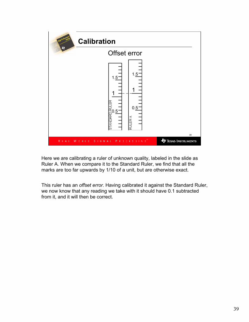
Here we are calibrating a ruler of unknown quality, labeled in the slide as
Ruler A. When we compare it to the Standard Ruler, we find that all the
marks are too far upwards by 1/10 of a unit, but are otherwise exact.
This ruler has an offset error. Having calibrated it against the Standard Ruler,
we now know that any reading we take with it should have 0.1 subtracted
from it, and it will then be correct.
40
40
Calibration
Gain error
1
0.5
1.5
1
0.5
1.5
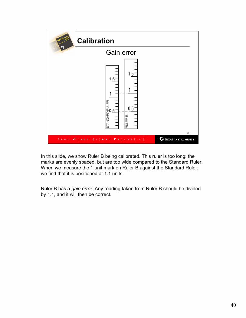
In this slide, we show Ruler B being calibrated. This ruler is too long: the
marks are evenly spaced, but are too wide compared to the Standard Ruler.
When we measure the 1 unit mark on Ruler B against the Standard Ruler,
we find that it is positioned at 1.1 units.
Ruler B has a gain error. Any reading taken from Ruler B should be divided
by 1.1, and it will then be correct.
41
41
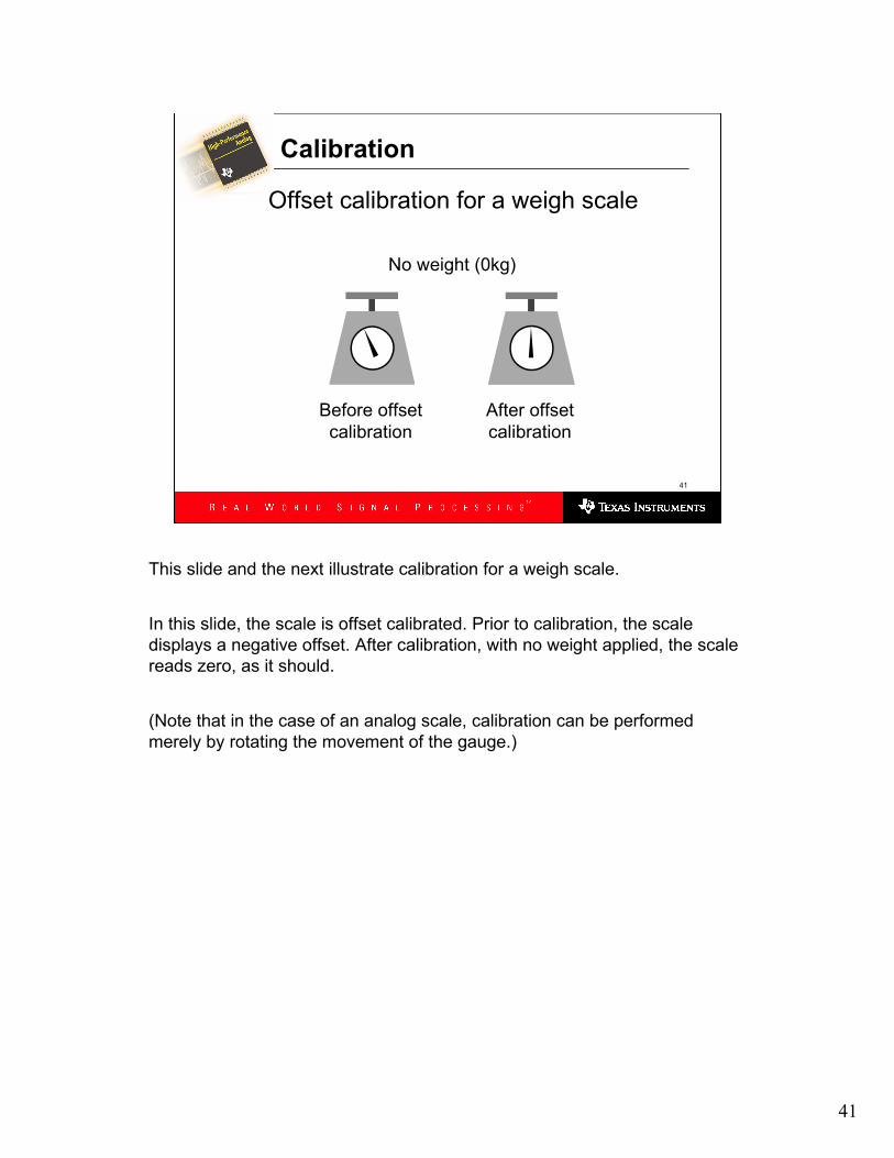
Calibration
Offset calibration for a weigh scale
Before offset
calibration
After offset
calibration
No weight (0kg)
This slide and the next illustrate calibration for a weigh scale.
In this slide, the scale is offset calibrated. Prior to calibration, the scale
displays a negative offset. After calibration, with no weight applied, the scale
reads zero, as it should.
(Note that in the case of an analog scale, calibration can be performed
merely by rotating the movement of the gauge.)

42
42
Calibration
Offset calibration for a weigh scale
Before gain
calibration
After offset
calibration
4.8kg
5kg Known weight
5kg
5kg Known weight
In this slide, the scale is shown being calibrated for gain. A known weight is
obtained and placed on the scale. The scale is then adjusted until its reading
is equal to the mass of the known weight.
This scale reads too low when the 5kg known weight is placed on it.
Following calibration, the scale reads 5kg with a 5kg known weight on it, as it
should.
43
43
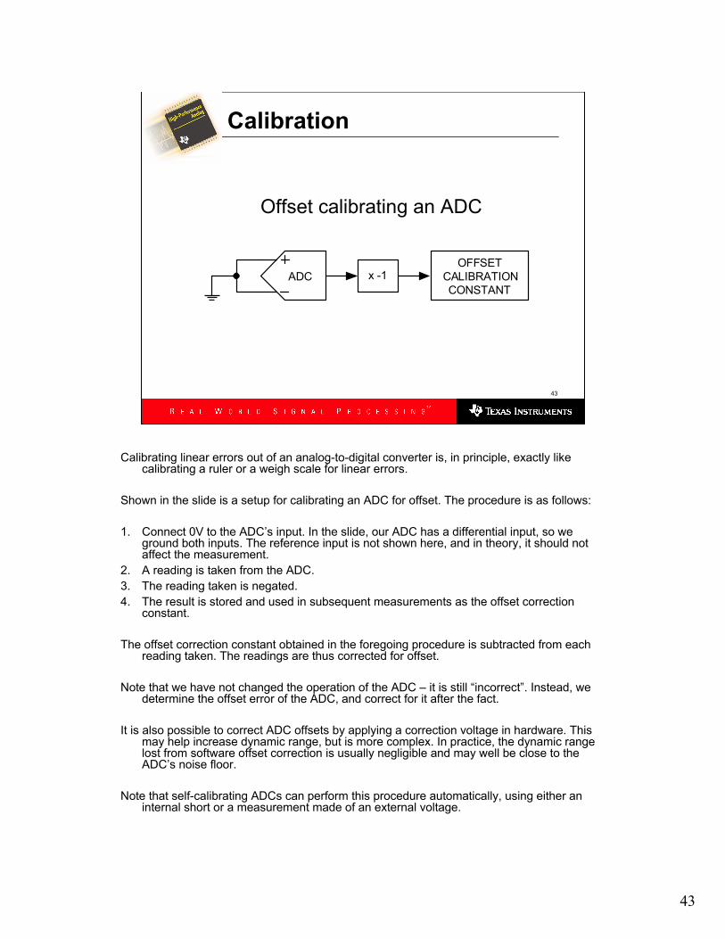
Calibration
Offset calibrating an ADC
ADC x -1OFFSET
CALIBRATION
CONSTANT
Calibrating linear errors out of an analog-to-digital converter is, in principle, exactly like calibrating a ruler or a weigh scale for linear errors.
Shown in the slide is a setup for calibrating an ADC for offset. The procedure is as follows:
1. Connect 0V to the ADC’s input. In the slide, our ADC has a differential input, so we ground both inputs. The reference input is not shown here, and in theory, it should not affect the measurement.
2. A reading is taken from the ADC.
3. The reading taken is negated.
4. The result is stored and used in subsequent measurements as the offset correction constant.
The offset correction constant obtained in the foregoing procedure is subtracted from each reading taken. The readings are thus corrected for offset.
Note that we have not changed the operation of the ADC – it is still “incorrect”. Instead, we determine the offset error of the ADC, and correct for it after the fact.
It is also possible to correct ADC offsets by applying a correction voltage in hardware. This may help increase dynamic range, but is more complex. In practice, the dynamic range lost from software offset correction is usually negligible and may well be close to the ADC’s noise floor.
Note that self-calibrating ADCs can perform this procedure automatically, using either an internal short or a measurement made of an external voltage.
44
44
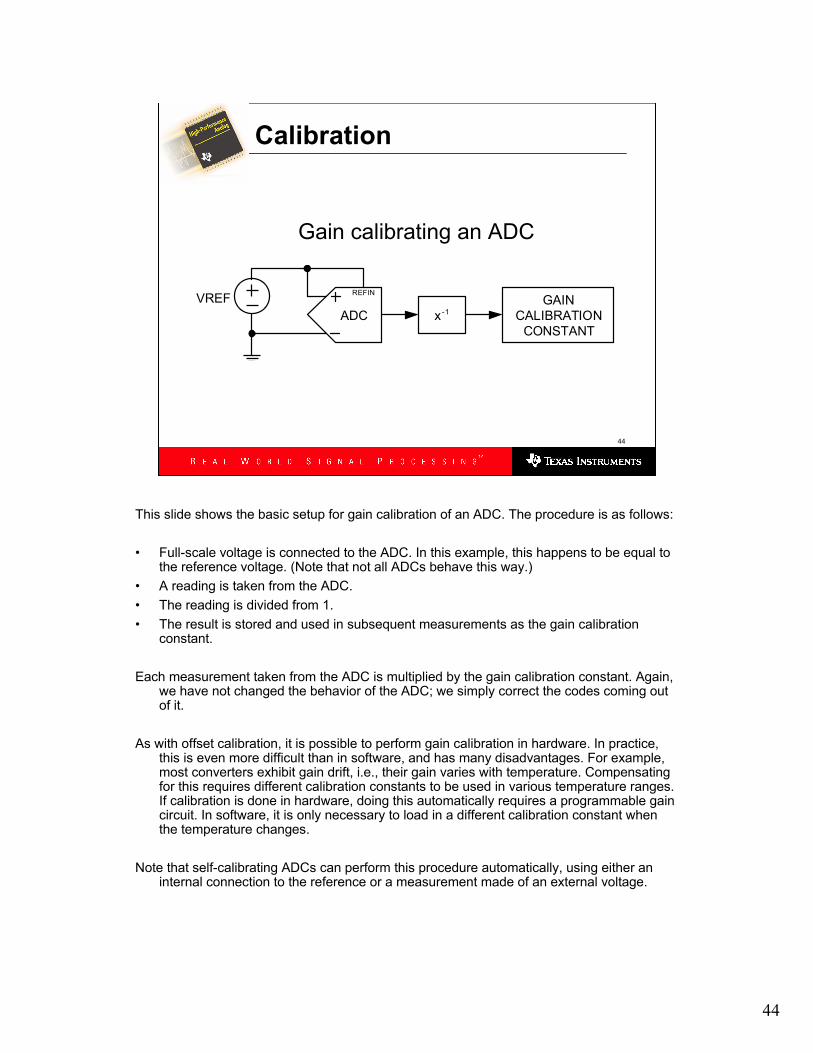
Calibration
Gain calibrating an ADC
ADC x -1
GAIN
CALIBRATION
CONSTANT
VREFREFIN
This slide shows the basic setup for gain calibration of an ADC. The procedure is as follows:
• Full-scale voltage is connected to the ADC. In this example, this happens to be equal to the reference voltage. (Note that not all ADCs behave this way.)
• A reading is taken from the ADC.
• The reading is divided from 1.
• The result is stored and used in subsequent measurements as the gain calibration constant.
Each measurement taken from the ADC is multiplied by the gain calibration constant. Again, we have not changed the behavior of the ADC; we simply correct the codes coming out of it.
As with offset calibration, it is possible to perform gain calibration in hardware. In practice, this is even more difficult than in software, and has many disadvantages. For example, most converters exhibit gain drift, i.e., their gain varies with temperature. Compensating for this requires different calibration constants to be used in various temperature ranges. If calibration is done in hardware, doing this automatically requires a programmable gain circuit. In software, it is only necessary to load in a different calibration constant when the temperature changes.
Note that self-calibrating ADCs can perform this procedure automatically, using either an internal connection to the reference or a measurement made of an external voltage.
45
45
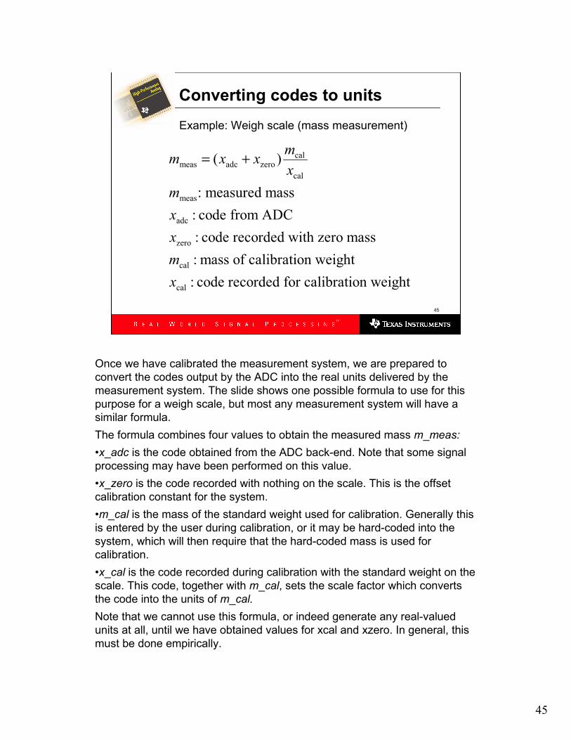
Converting codes to units
calmeas adc zero
cal
meas
adc
zero
cal
cal
( )
: measured mass
: code from ADC
: code recorded with zero mass
: mass of calibration weight
: code recorded for calibration weight
mm x x
x
m
x
x
m
x
= +
Example: Weigh scale (mass measurement)
Once we have calibrated the measurement system, we are prepared to
convert the codes output by the ADC into the real units delivered by the
measurement system. The slide shows one possible formula to use for this
purpose for a weigh scale, but most any measurement system will have a
similar formula.
The formula combines four values to obtain the measured mass m_meas:
•x_adc is the code obtained from the ADC back-end. Note that some signal
processing may have been performed on this value.
•x_zero is the code recorded with nothing on the scale. This is the offset
calibration constant for the system.
•m_cal is the mass of the standard weight used for calibration. Generally this
is entered by the user during calibration, or it may be hard-coded into the
system, which will then require that the hard-coded mass is used for
calibration.
•x_cal is the code recorded during calibration with the standard weight on the
scale. This code, together with m_cal, sets the scale factor which converts
the code into the units of m_cal.
Note that we cannot use this formula, or indeed generate any real-valued
units at all, until we have obtained values for xcal and xzero. In general, this
must be done empirically.
46
46
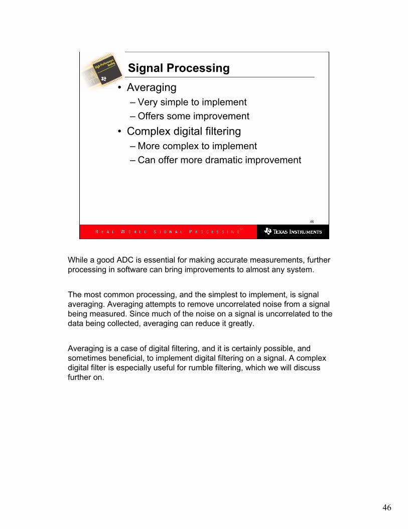
Signal Processing
• Averaging
– Very simple to implement
– Offers some improvement
• Complex digital filtering
– More complex to implement
– Can offer more dramatic improvement
While a good ADC is essential for making accurate measurements, further
processing in software can bring improvements to almost any system.
The most common processing, and the simplest to implement, is signal
averaging. Averaging attempts to remove uncorrelated noise from a signal
being measured. Since much of the noise on a signal is uncorrelated to the
data being collected, averaging can reduce it greatly.
Averaging is a case of digital filtering, and it is certainly possible, and
sometimes beneficial, to implement digital filtering on a signal. A complex
digital filter is especially useful for rumble filtering, which we will discuss
further on.

47
47
Basic Averaging
ave
0
1 N
i
i
x xN
=
= ∑
sig
aveN
σ
σ =
The two primary kinds of signal averaging are coherent and incoherent averaging. The terms apply primarily to non-DC signal situations. When we are measuring a signal that is essentially DC, the averaging is always coherent; since our primary focus here is on near-DC signals, we will not discuss these terms further.
(A thorough discussion of digital signal averaging can be found in Understanding Digital Signal Processing by Richard G. Lyons [1997], ISBN 0-201-63467-8, chapter 9. This book is highly recommended for anyone performing any level of digital signal processing. Several figures from this book appear in this presentation.)
The process of averaging is well known: the numbers to be averaged are summed, and divided by the number of them, as shown in the top equation.
When averaging is coherent – i.e., the signal remains constant, while the noise changes –the noise, being uncorrelated, averages out. The more averaging performed, the more the noise cancels. If the signal is DC, and the noise component is random, then with each successive sample averaged, the signal-to-noise ratio will improve.
In fact, it can be shown that the improvement is proportional to the square root of the number of samples in the average. The second equation illustrates this: the standard deviation of the average of a number of noisy samples of the same signal is the standard deviation of the original signal divided by the square root of N. Therefore, there is a diminishing return associated with averaging.
The second equation assumes that each averaged signal is the same. In reality, this is not the case, as no real signal is exactly at DC. Any quantity we measure will exhibit some level of slow drift, and this will appear in averages over time. This limits the effectiveness of large numbers of averages.
48
48
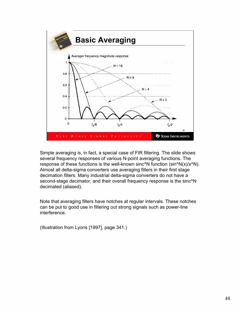
Basic Averaging
Simple averaging is, in fact, a special case of FIR filtering. The slide shows
several frequency responses of various N-point averaging functions. The
response of these functions is the well-known sinc^N function (sin^N(x)/x^N).
Almost all delta-sigma converters use averaging filters in their first stage
decimation filters. Many industrial delta-sigma converters do not have a
second-stage decimator, and their overall frequency response is the sinc^N
decimated (aliased).
Note that averaging filters have notches at regular intervals. These notches
can be put to good use in filtering out strong signals such as power-line
interference.
(Illustration from Lyons [1997], page 341.)
49
49
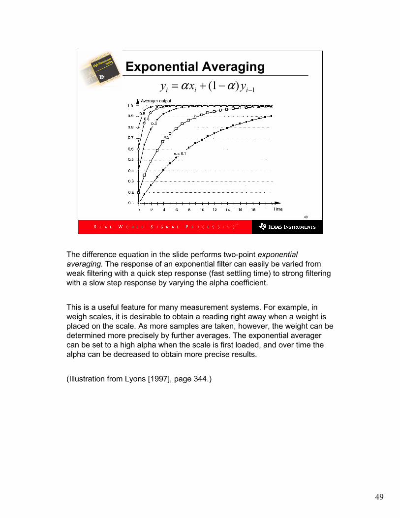
Exponential Averaging
1(1 )i i iy x yα α−
= + −
The difference equation in the slide performs two-point exponential
averaging. The response of an exponential filter can easily be varied from
weak filtering with a quick step response (fast settling time) to strong filtering
with a slow step response by varying the alpha coefficient.
This is a useful feature for many measurement systems. For example, in
weigh scales, it is desirable to obtain a reading right away when a weight is
placed on the scale. As more samples are taken, however, the weight can be
determined more precisely by further averages. The exponential averager
can be set to a high alpha when the scale is first loaded, and over time the
alpha can be decreased to obtain more precise results.
(Illustration from Lyons [1997], page 344.)
50
50
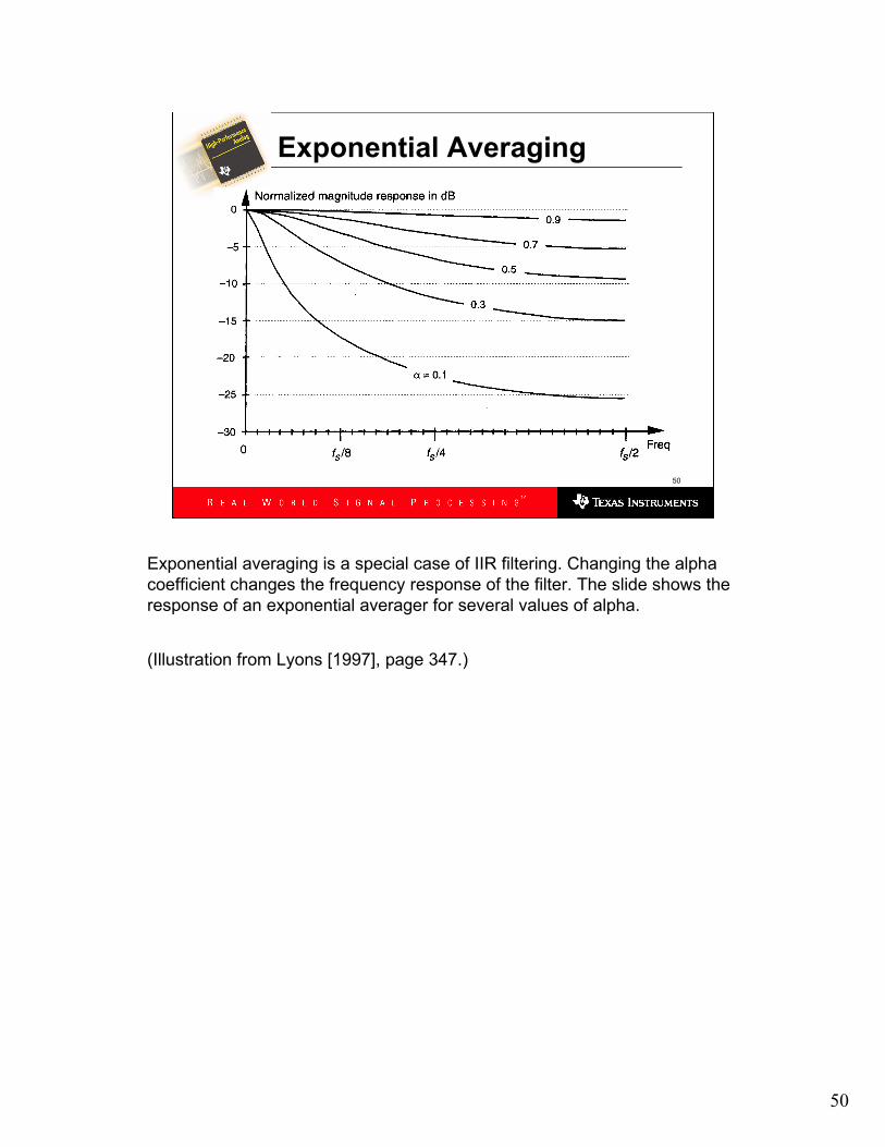
Exponential Averaging
Exponential averaging is a special case of IIR filtering. Changing the alpha
coefficient changes the frequency response of the filter. The slide shows the
response of an exponential averager for several values of alpha.
(Illustration from Lyons [1997], page 347.)
51
51
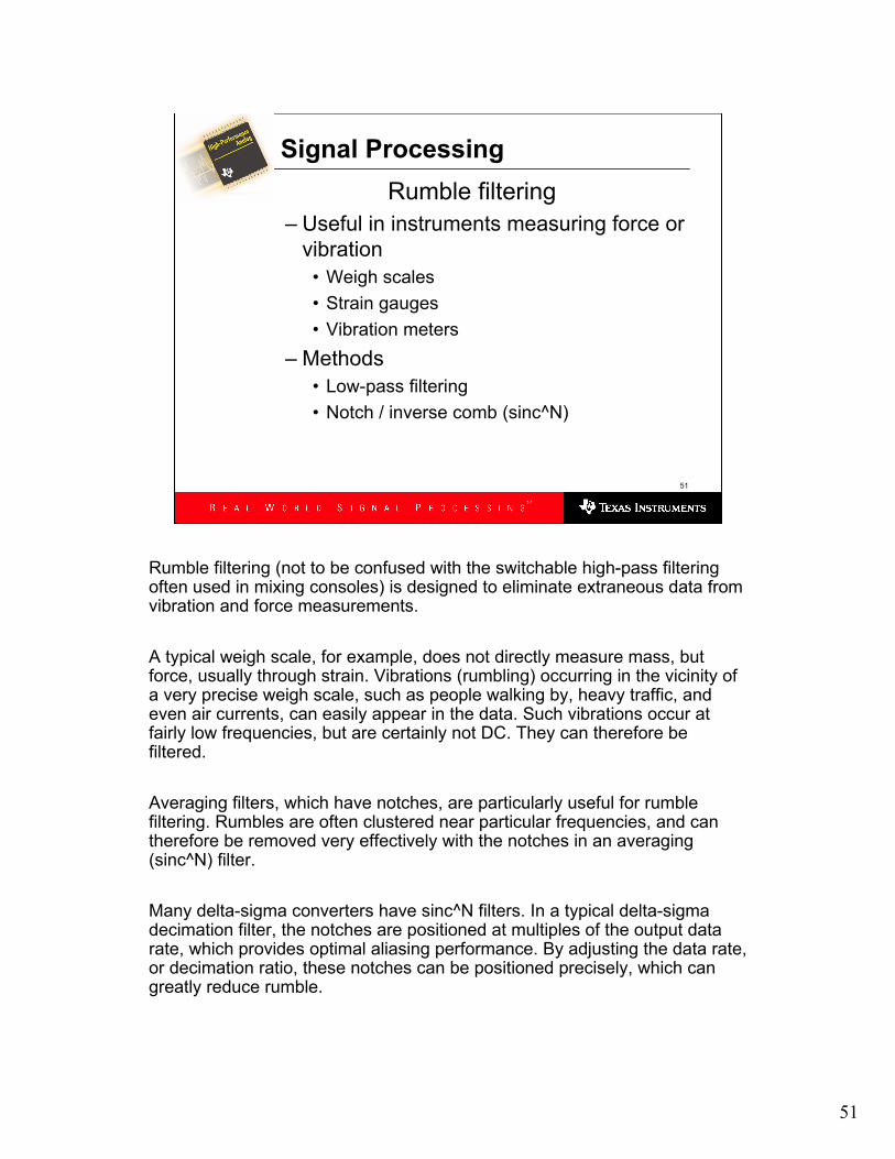
Signal Processing
Rumble filtering
– Useful in instruments measuring force or
vibration
• Weigh scales
• Strain gauges
• Vibration meters
– Methods
• Low-pass filtering
• Notch / inverse comb (sinc^N)
Rumble filtering (not to be confused with the switchable high-pass filtering often used in mixing consoles) is designed to eliminate extraneous data from vibration and force measurements.
A typical weigh scale, for example, does not directly measure mass, but force, usually through strain. Vibrations (rumbling) occurring in the vicinity of a very precise weigh scale, such as people walking by, heavy traffic, and even air currents, can easily appear in the data. Such vibrations occur at fairly low frequencies, but are certainly not DC. They can therefore be filtered.
Averaging filters, which have notches, are particularly useful for rumble filtering. Rumbles are often clustered near particular frequencies, and can therefore be removed very effectively with the notches in an averaging (sinc^N) filter.
Many delta-sigma converters have sinc^N filters. In a typical delta-sigma decimation filter, the notches are positioned at multiples of the output data rate, which provides optimal aliasing performance. By adjusting the data rate, or decimation ratio, these notches can be positioned precisely, which can greatly reduce rumble.