Embed Size (px)
Citation preview

INTEGRATION METHODS FOR ENHANCED TRAPPING ANDSPECTROSCOPY IN OPTOFLUIDICS
Praveen Cheriyan Ashok
A Thesis Submitted for the Degree of PhDat the
University of St. Andrews
2012
Full metadata for this item is available inResearch@StAndrews:FullText
at:http://research-repository.st-andrews.ac.uk/
Please use this identifier to cite or link to this item:http://hdl.handle.net/10023/2546
This item is protected by original copyright
Integration Methods for Enhanced Trapping and
Spectroscopy in Optofluidics
Praveen Cheriyan Ashok
This thesis is submitted for the degree of Doctor of Philosophy at the
University of St Andrews
Optical Manipulation & Microphotonics Groups
School of Physics & Astronomy
University of St Andrews
October 2011

Dedicated to: Love of my life, Bavishna,
My dear parents and beloved sister
ൻ !"
Integration Methods for Enhanced Trapping and Spectroscopy in Optofluidics
Praveen Cheriyan Ashok
Submitted for the degree of Doctor of Philosophy October 2011
iv
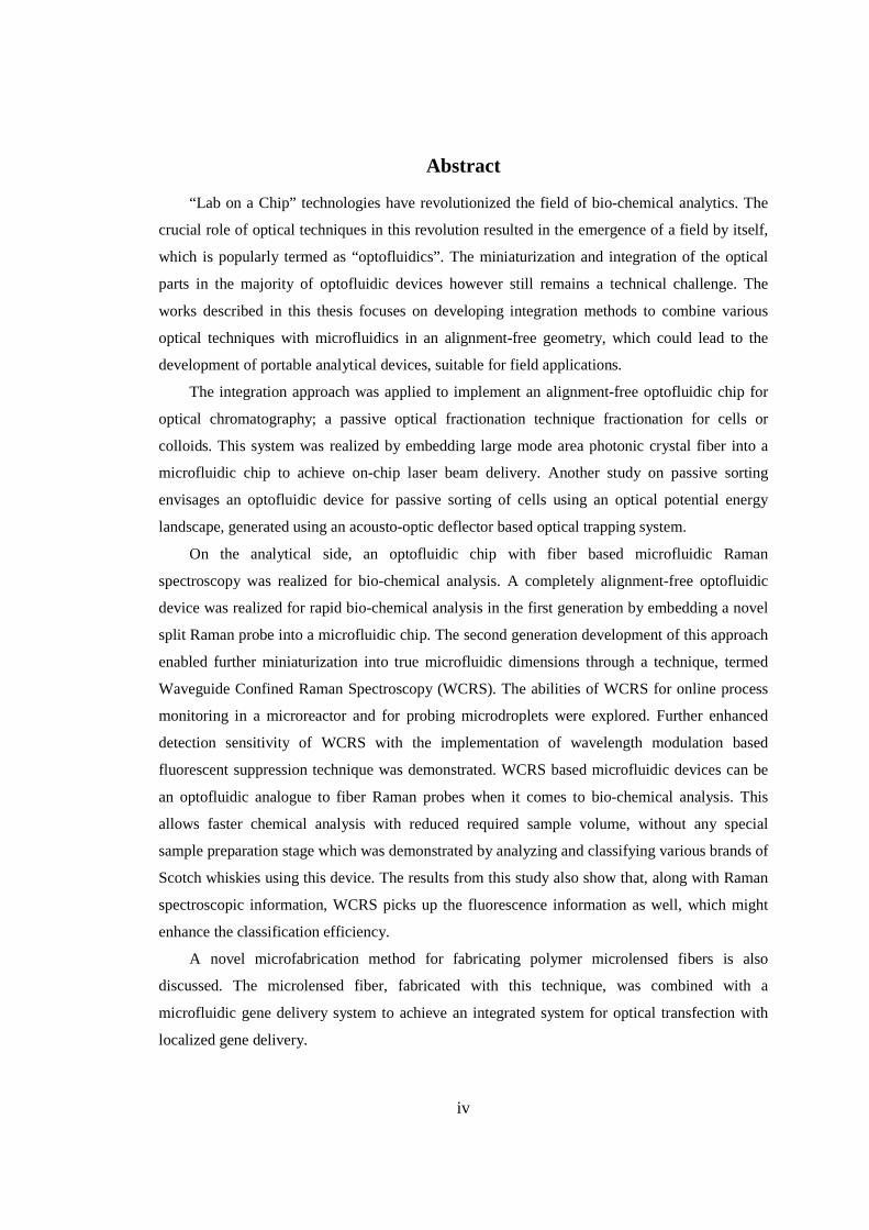
Abstract
“Lab on a Chip” technologies have revolutionized the field of bio-chemical analytics. The
crucial role of optical techniques in this revolution resulted in the emergence of a field by itself,
which is popularly termed as “optofluidics”. The miniaturization and integration of the optical
parts in the majority of optofluidic devices however still remains a technical challenge. The
works described in this thesis focuses on developing integration methods to combine various
optical techniques with microfluidics in an alignment-free geometry, which could lead to the
development of portable analytical devices, suitable for field applications.
The integration approach was applied to implement an alignment-free optofluidic chip for
optical chromatography; a passive optical fractionation technique fractionation for cells or
colloids. This system was realized by embedding large mode area photonic crystal fiber into a
microfluidic chip to achieve on-chip laser beam delivery. Another study on passive sorting
envisages an optofluidic device for passive sorting of cells using an optical potential energy
landscape, generated using an acousto-optic deflector based optical trapping system.
On the analytical side, an optofluidic chip with fiber based microfluidic Raman
spectroscopy was realized for bio-chemical analysis. A completely alignment-free optofluidic
device was realized for rapid bio-chemical analysis in the first generation by embedding a novel
split Raman probe into a microfluidic chip. The second generation development of this approach
enabled further miniaturization into true microfluidic dimensions through a technique, termed
Waveguide Confined Raman Spectroscopy (WCRS). The abilities of WCRS for online process
monitoring in a microreactor and for probing microdroplets were explored. Further enhanced
detection sensitivity of WCRS with the implementation of wavelength modulation based
fluorescent suppression technique was demonstrated. WCRS based microfluidic devices can be
an optofluidic analogue to fiber Raman probes when it comes to bio-chemical analysis. This
allows faster chemical analysis with reduced required sample volume, without any special
sample preparation stage which was demonstrated by analyzing and classifying various brands of
Scotch whiskies using this device. The results from this study also show that, along with Raman
spectroscopic information, WCRS picks up the fluorescence information as well, which might
enhance the classification efficiency.
A novel microfabrication method for fabricating polymer microlensed fibers is also
discussed. The microlensed fiber, fabricated with this technique, was combined with a
microfluidic gene delivery system to achieve an integrated system for optical transfection with
localized gene delivery.

v
Declaration
1. Candidate’s declarations:
I, Praveen Cheriyan Ashok, hereby certify that this thesis, which is approximately 45000 words in
length, has been written by me, that it is the record of work carried out by me and that it has not
been submitted in any previous application for a higher degree.
I was admitted as a research student in September 2008 and as a candidate for the degree of
Doctor of Philosophy in Physics in September 2008; the higher study for which this is a record
was carried out in the University of St Andrews between 2008 and 2011.
Date …… signature of candidate ………
2. Supervisor’s declaration:
I hereby certify that the candidate has fulfilled the conditions of the Resolution and Regulations
appropriate for the degree of Doctor of Philosophy in the University of St Andrews and that the
candidate is qualified to submit this thesis in application for that degree.
Date …… signature of supervisor ………
3. Permission for electronic publication: (to be signed by both candidate and supervisor)
In submitting this thesis to the University of St Andrews I understand that I am giving permission
for it to be made available for use in accordance with the regulations of the University Library for
the time being in force, subject to any copyright vested in the work not being affected thereby. I
also understand that the title and the abstract will be published, and that a copy of the work may
be made and supplied to any bona fide library or research worker, that my thesis will be
electronically accessible for personal or research use unless exempt by award of an embargo as
requested below, and that the library has the right to migrate my thesis into new electronic forms
as required to ensure continued access to the thesis. I have obtained any third-party copyright
permissions that may be required in order to allow such access and migration, or have
requested the appropriate embargo below.
The following is an agreed request by candidate and supervisor regarding the electronic
publication of this thesis: Access to printed copy and electronic publication of thesis through the
University of St Andrews.
Date …… signature of candidate …… signature of supervisor ………
vi
Acknowledgements
The first and foremost person to be acknowledged would be my supervisor, Prof.
Kishan Dholakia for giving me this opportunity to do research under his guidance in the
optical manipulation group. He was a constant source of inspiration and encouragement
throughout my PhD studies. He gave me enough freedom and supported me throughout
all the research and academic endeavors I have taken during these years which helped
me to expand my skills and experiences. Special thanks to my second supervisor, Prof.
Thomas Krauss for the opportunity he gave to work in his group and his constant support
through discussions and suggestions. I would also like to express my thanks to Prof.
Frank Gunn-Moore for the help and support he has given me during these years.
In the last three years I had the opportunity to collaborate and work with several
outstanding researchers, to whom I would like to express my special thanks and
gratitude. Robert Marchington is a person who has given me all support from the very
beginning of my PhD studies. He has spent a considerable amount of time to train me on
fabrication methods and to discuss various aspects of my research activities. A very
special thanks to him for all the support he has given me throughout these years. Another
person who has influenced my research was Gajendra Pratap Singh, who introduced me
to the world of Raman spectroscopy. I would also like to express my gratitude to Tomas
Cizmar, who spent his valuable time giving me training in new technologies. I have
enjoyed working with Nan Ma, David Stevenson, Helen Rendall, Mark Scullion and
Heather Dalgarno. Without mentioning names I would like to express my gratitude to all
my colleagues in the group for their friendship which made my life enjoyable for last
three years.
Special thanks to all the administrative staffs and technical staffs whose help and
support made my life hassle-free for the last few years. Thanks to Scott Johnston in the
stores for all the helps he has given me. Steve Balfour and George Robb deserve special
mention for resolving all issues related to cleanroom so quickly making my research life
really smooth. Thanks to David Steven and all in workshop who were always prompt in
dealing with my request. Also thanks to Mark Ross and Chris Booth for solving
electronic related issues promptly.

vii
A special thanks to Robert Marchington, Heather Dalgarno, Prof. Frank Gunn-
Moore and Christopher Reardon, who helped me to polish the content of this thesis by
proof reading and suggesting corrections.
I should express special gratitude to Bavishna Balagopal, who is my colleague as
well as my lovely wife. She has always supported me and encouraged me for all my
endeavors. Thanks to Bavi, for filling my professional and personal life with loads of
happiness.
On a more personal note I would like to express my thanks to my parents, my sister
and my in-laws for their love and support throughout these years.
viii
Publications
Peer reviewed journals
• Ashok PC, Marchington RF, Mthunzi P, Krauss TF, Dholakia K (2010) Optical
chromatography using a photonic crystal fiber with on-chip fluorescence
excitation. Opt Express 18 (6):6396-6407
• Ashok PC, Singh GP, Tan KM, Dholakia K (2010) Fiber probe based
microfluidic raman spectroscopy. Opt Express 18 (8):7642-7649
• Ma N, Ashok PC, Stevenson DJ, Gunn-Moore FJ, Dholakia K (2010) Integrated
optical transfection system using a microlens fiber combined with microfluidic
gene delivery. Biomed Opt Express 1 (2):694-705. doi:10.1364/BOE.1.000694
• Ashok PC, Singh GP, Rendall HA, Krauss TF, Dholakia K (2011) Waveguide
confined Raman spectroscopy for microfluidic interrogation. Lab Chip 11
(7):1262 - 1270. doi:10.1039/c0lc00462f
• Ashok PC, Luca ACD, Mazilu M, Dholakia K (2011) Enhanced bioanalyte
detection in waveguide confined Raman spectroscopy using modulation
techniques. J Biophot 4 (7-8):514-518. doi:10.1002/jbio.201000107
• Čižmár T, Dalgarno HIC, Ashok PC, Gunn-Moore FJ, Dholakia K (2011)
Interference-free superposition of non-zero order light modes: Functionalized
optical landscapes. Appl Phys Lett. doi:10.1063/1.3552202
• Čižmár T, Dalgarno HIC, Ashok PC, Gunn-Moore FJ, Dholakia K (2011)
Optical aberration compensation in a multiplexed optical trapping system.
Journal of Optics 13 (4):044008. doi:10.1088/2040-8978/13/4/044008
• James TD, Scullion MG, Ashok PC, Di Falco AD, Dholakia K, Krauss TF
(2011) Valve controlled fluorescence detection system for remote sensing
applications. Microfluidics and Nanofluidics: 1-8. doi:10.1007/s10404-011-
0818-1
• Ashok PC, Praveen BB, Dholakia K (2011) Near infrared spectroscopic analysis
of single malt scotch whisky on an optofluidic chip. Opt Express 19 (23):22982-
22992. doi:10.1364/OE.19.022982
ix
• Ashok PC, Dholakia K (2011) Optical trapping for analytical biotechnology.
Curr Opin Biotech. doi:10.1016/j.copbio.2011.11.011 (Review paper)
Book Chapter
• Ashok PC, Dholakia K (under review) Microfluidic Raman spectroscopy for
bio-chemical sensing and analysis. In: Fritzsche W, Popp J (eds) Springer series
on chemical sensors and biosensors: Optical nano- and microsystems for
bioanalytics. Springer,
Patents
• Application: The University of St. Andrews Ashok PC, Singh GP, Dholakia K,
“Filterless Fiber Probe Based Microfluidic Raman Spectroscopy”, International
Patent Application No. PCT/GB2011/001406
• Application: The University of St. Andrews, Ashok PC, Singh GP, Dholakia K,
Tan KM “Fiber-based microfluidic Raman spectroscopy” Application No. US
12/892,640, CA 2,715,886.
• Application: The University of St. Andrews, Ma N, Ashok PC, Stevenson DJ,
Dholakia K, Gunn-Moore FJ, “ Microlensed fiber based poration”
PCT/GB2011/000881
• Application: The University of St. Andrews, Marchington RF, Ashok P,
Dholakia K., “Optical Trap”, WO/2010/007371 A2
Conference Publications
• Ashok PC, Marchington RF, Mazilu M, Krauss TF, Dholakia K Towards
integrated optical chromatography using photonic crystal fiber. In: Dholakia K,
Spalding CG (eds), 2009. SPIE, p 74000R (Oral Presentation)
• Dharanipathy UP, Falco AD, Scullion MG, Ashok PC, Marchington RF, Krauss
TF (2009) An integrated slotted photonic crystal biosensor array. Paper presented
at the EOS Topical Meeting on "Blue" Photonics - Optics in the Sea Aberdeen,
x
• Ashok PC, Singh GP, Tan KM, Dholakia K (2010) Microfluidic raman
spectroscopy for bioanalyte detection Paper presented at the International
Conference on Raman Spectroscopy, Boston, US. (Poster presentation)
• Singh GP, Tan KM, Ashok PC, Herrington CS, Sibbett W, Brown CTA (2010)
Surgical raman forceps for disease diagnosis. Paper presented at the International
Conference on Raman Spectroscopy, Boston, US,
• Ashok PC, Singh GP, Luca ACD, Mazilu M, Dholakia K (2010) Embedded
fiber probes for raman spectroscopic detection in microfluidics. Paper presented
at the Photonics 2010, Guwahati, India, (Oral Presentation)
• Ma N, Ashok PC, Gunn-Moore FJ, Dholakia K Fabrication of polymer
microlens at the apex of optical fiber. In, 2010. vol 1. SPIE, p 817314 (Oral
presentation)
• Cizmar T, Mazilu M, Dalgarno H, Ashok P, Gunn-Moore F, Dholakia K Optical
sculpting: Trapping through disorder and transfer of orbital angular momentum.
In: Andrews DL, Galvez EJ, Gluckstad J (eds), San Francisco, California, USA,
2011. SPIE, pp 79500R-79507
• Ashok PC, Dholakia K (2011) Integration methods for raman spectroscopy and
passive sorting in optofluidics. Paper presented at the Frontiers in Optics, San
Jose, US, (Invited Talk)
• Ashok PC, Dholakia K (2011) Passive fractionation of colloids and cells using
optofluidics. Paper presented at the Saratov Fall Meeting, Saratov, (Internet
invited lecture)
xi
List of Abbreviations
CAD Computer Aided Design
CHO-K1 Chinese Hamster Ovary cells
DA-AOD Dual Axis-Acousto Optic Deflector
DAQ data acquisition
DFS digital frequency synthesizer
DHM Digital Holographic Microscopy
EOF electroosmotic flow
FACS fluorescence activated cell sorting
FCS fetal calf serum
FIFO first in first out
FRET fluorescence resonance energy transfer
fs Femtosecond
GVD Group Velocity Dispersion
HEK-293 Human Embryonic Kidney Cells
HF Hydrogen Fluoride
HWP half wave plate
impf iterative modified polynomial fitting
IPA isopropanol
IR Infra-Red
LMA PCF Large Mode Area Photonic Crystal Fiber
LoC Lab on a Chip
MRS Microfluidic Raman Spectroscopy
NA numerical aperture

xii
ND Neutral Density
NEC Noise Equivalent Concentration
OCT Optical Coherence Tomography
OH hydroxyl
PBS polarizing beam splitter
PC Principle Component
PCA Principle Component Analysis
PCF Photonic Crystal Fiber
PDMS polydimethylsiloxane
PLS Partial Least Square
RACS Raman activated cell sorting
RBC red blood cells
RMSEP root mean square error of prediction
rpm revolutions per minute
SERRS Surface Enhanced Resonance Raman Spectroscopy
SERS Surface Enhanced Raman Spectroscopy
SNR Signal to Noise Ratio
SPM Self-Phase Modulation
TNT trinitrotoluene
TR3 time resolved resonance Raman spectroscopy
UV ultraviolet
WCRS Waveguide Confined Raman Spectroscopy

xiii
Table of Contents
Abstract ............................................................................................................................. iv
Declaration ......................................................................................................................... v
Acknowledgements ........................................................................................................... vi
Publications ..................................................................................................................... viii
Peer reviewed journals .............................................................................................. viii
Book Chapter .............................................................................................................. ix
Patents ......................................................................................................................... ix
Conference Publications ............................................................................................. ix
List of Abbreviations ........................................................................................................ xi
Table of Contents ............................................................................................................ xiii
1. Introduction .................................................................................................................. 1
2. Microfluidics – Physics & Fabrication Techniques ..................................................... 4
2.1 Introduction ........................................................................................................ 4
2.2 Fluid dynamics at low Reynolds number ........................................................... 5
2.3 Microfabrication using soft-lithography ............................................................ 7
2.3.1 Design of the mask ................................................................................. 9
2.3.2 Fabrication of the master mold .............................................................. 9
2.3.3 Fabrication of PDMS chip using soft-lithography ............................... 12
2.4 Embedding fiber into a PDMS microfluidic chip ............................................ 15
2.5 PDMS membrane based microfluidic fabrication ............................................ 17
2.6 Microfluidic channels with optical windows on both sides ............................. 17
2.7 Paraffin microvalve .......................................................................................... 19
2.8 Conclusion ....................................................................................................... 21
Relevant publications ................................................................................................. 22
Contributions ............................................................................................................. 22
xiv
3. Integrated optical chromatography using photonic crystal fiber ............................... 23
3.1 Introduction ...................................................................................................... 23
3.2 Theory of optical chromatography ................................................................... 25
3.3 History of optical chromatography .................................................................. 27
3.4 Optical Chromatography with on-chip light delivery – Rationale ................... 31
3.5 Design of optical chromatography chip with on-chip fiber light delivery ....... 32
3.5.1 Choice of the fiber – Large Mode Area Photonic Crystal Fiber (LMA-PCF) ..................................................................................................... 32
3.5.2 Chip design and fabrication ................................................................. 34
3.6 Optical setup..................................................................................................... 39
3.7 Fluidic setup ..................................................................................................... 41
3.8 Calibration of the system ................................................................................. 42
3.9 On-chip fluorescence excitation ....................................................................... 45
3.10 Verification of the purity of spatially separated samples ................................. 46
3.11 Separation of mammalian cells incubated with polystyrene beads .................. 47
3.12 Conclusion ....................................................................................................... 49
Relevant Publications ................................................................................................ 51
Patent ......................................................................................................................... 51
Contributions ............................................................................................................. 51
4. Towards passive optical cell sorting in an optofluidic chip using optical landscapes52
4.1 Introduction ...................................................................................................... 52
4.2 Optical trapping system with a DA- AOD – optical design and interface ....... 53
4.2.1 DA-AOD controller ............................................................................. 56
4.2.2 LabVIEW interface .............................................................................. 57
4.3 Theory of optical landscape sorting using a line trap ...................................... 58
4.4 In-situ calibration for optimizing parameters for sorting cells......................... 61
4.5 Conclusion ....................................................................................................... 65
Contributions ............................................................................................................. 67

xv
5. Fiber probe based microfluidic Raman spectroscopy ................................................ 68
5.1 Introduction ...................................................................................................... 68
5.2 Raman spectroscopy......................................................................................... 69
5.3 History of microfluidic Raman spectroscopy .................................................. 71
5.3.1 Initial studies ........................................................................................ 72
5.3.2 Raman spectroscopy to probe reactions ............................................... 73
5.3.3 Bio-chemical detection using SERS microfluidics .............................. 74
5.3.4 Raman spectroscopic probing of microdroplets ................................... 75
5.3.5 Microfluidic Raman spectroscopy in cell science ................................ 76
5.3.6 Recent Developments........................................................................... 77
5.4 Fiber probe based microfluidic Raman spectroscopy – Rationale ................... 78
5.5 Design of the split Raman probe ...................................................................... 80
5.6 Chip design and fabrication ............................................................................. 82
5.7 Detection device ............................................................................................... 83
5.8 Optimizing the collection geometry ................................................................. 84
5.9 Detection limit of the microfluidic device with the embedded probe .............. 86
5.10 Effect of flow ................................................................................................... 88
5.11 Residual free nature of the chip ....................................................................... 88
5.12 Conclusions ...................................................................................................... 89
Relevant publications ................................................................................................. 90
Patent ......................................................................................................................... 91
Publicity ..................................................................................................................... 91
Contribution ............................................................................................................... 91
6. Waveguide Confined Raman Spectroscopy (WCRS) ............................................... 92
6.1 Introduction ...................................................................................................... 92
6.2 Embedding fiber into the microfluidic chip ..................................................... 94
6.3 Raman detection system ................................................................................... 94

xvi
6.4 Characterization of the device .......................................................................... 95
6.4.1 The effect of collection angle ............................................................... 97
6.4.2 The effect of fiber length...................................................................... 98
6.4.3 The effect of fiber core size ................................................................. 99
6.5 Minimum detection limit for urea .................................................................. 100
6.6 Monitoring of micro-reaction in a micro-reactor ........................................... 101
6.7 Detection of microdroplets using WCRS ....................................................... 105
6.8 Conclusion ..................................................................................................... 107
Relevant publications ............................................................................................... 108
Patent ....................................................................................................................... 109
Publicity ................................................................................................................... 109
Contribution ............................................................................................................. 109
7. Enhanced bioanalyte detection in waveguide confined Raman spectroscopy using wavelength modulation ............................................................................................ 110
7.1 Introduction .................................................................................................... 110
7.2 Wavelength modulation implemented in a WCRS device ............................. 110
7.3 Raman acquisition method ............................................................................. 112
7.4 Detection sensitivity ....................................................................................... 112
7.5 Conclusion ..................................................................................................... 115
Relevant publications ............................................................................................... 116
Contributions ........................................................................................................... 116
8. Near infrared spectroscopic analysis of single malt scotch whisky in an optofluidic chip .......................................................................................................................... 117
8.1 Introduction .................................................................................................... 117
8.2 Experimental .................................................................................................. 119
8.3 Results and discussions .................................................................................. 121
8.3.1 Concentration estimation ................................................................... 122
8.3.2 Classification of whisky samples ....................................................... 124
xvii
8.3.3 Effect of photo-bleaching ................................................................... 127
8.3.4 Reproducibility ................................................................................... 129
8.4 Conclusion ..................................................................................................... 130
Relevant publications ............................................................................................... 131
Publicity ................................................................................................................... 131
Contributions ........................................................................................................... 131
9. Fabrication of microlens fiber combined with microfluidic gene delivery for integrated optical transfection .................................................................................. 132
9.1 Introduction .................................................................................................... 132
9.2 Fabrication of microlens tipped fiber ............................................................. 134
9.3 Characterization and modeling of the microstick .......................................... 138
9.4 Fabrication and characterization of collimating microlens ............................ 140
9.5 Cell transfection using microlens fiber .......................................................... 142
9.6 Design of a wholly integrated system for localized drug delivery................. 144
9.7 Efficiency of optical transfection ................................................................... 146
9.8 Conclusion ..................................................................................................... 148
Relevant publications ............................................................................................... 149
Patent ....................................................................................................................... 149
Contributions ........................................................................................................... 150
10. Conclusions & Future Outlook ................................................................................ 151
10.1 Summary of the thesis .................................................................................... 151
10.2 Future outlook ................................................................................................ 155
10.2.1 Optical chromatography ..................................................................... 156
10.2.2 Periodic optical landscape based passive optical cell sorting ............ 156
10.2.3 WCRS 157
10.2.4 Polymer microlensed fiber fabrication ............................................... 158
10.3 Conclusion ..................................................................................................... 158

xviii
Appendix 1 – Cell Preparation Protocols for the Optical Chromatography Experiments ................................................................................................................................. 159
Protocol for the photo-transfection of HEK-293 cells ................................... 159
Protocol for the incubation of HEK-293 cells with microspheres ................. 159
Bibliography .................................................................................................................. 161
1
1. Introduction
The advancements in microfluidics technologies have revolutionized the field of
bio-chemical analytics. Optical technologies have played a crucial role in realizing the
dream of implementing “Lab on a Chip (LoC)”. Hence the term “optofluidics” has
emerged in recent years to address technologies where optical techniques are used on a
microfluidic platform to obtain desired functionality. While optical techniques such as
imaging and spectroscopy may be used to probe the sample in the microfluidic channel,
the use of optical micromanipulation allowed manipulation of microscopic particles
within the microfluidic channel.
The majority of such technologies have further room for improvement in terms of
the miniaturization and integration of the optical systems to achieve truly portable
devices, suitable for field applications. This thesis mainly focuses on these aspects
developing optofluidic technologies for enhanced sorting and bio-chemical analysis with
special emphasize upon integration or embedding optical components within the
microfluidic chip to make it alignment-free and portable. Although there is this common
theme for the studies described in this thesis, they have diverse fields of application.
Hence, instead of general review chapters in the beginning of this thesis, a brief review
within the areas of application is given at the beginning of each chapter. The studies
described in this chapter can be mainly divided into three categories. Micro-fabrication
techniques, which are detailed in chapter 2 and chapter 9, optofluidic cell sorting, which
is described in chapter 3 and chapter 4 and optofluidic bio-chemical analytics using
Raman spectroscopy, discussed in chapter 5 to chapter 8.
Chapter 2 discusses the basic physical principles that govern fluid dynamics at the
microfluidic scale. Also this chapter explains in detail the soft lithographic fabrication
protocol for microfluidic chip fabrication, along with minor modification to protocols,
implemented to achieve integration of optical techniques to a microfluidic platform. The
chapter also describes the implementation of a close-open paraffin microvalve which can
be used for sensing applications.
Chapter 3 discusses a passive optical fractionation technique – “optical
chromatography”, which was implemented by embedding a photonic crystal fiber (PCF)
into the chip for on-chip beam delivery. The ability of this alignment-free chip to
2
achieve refractive index driven and size driven fractionation was demonstrated. Also
optical chromatographic fractionation of the sample combined with on-chip fluorescent
excitation was demonstrated by exploiting the endlessly single mode nature of PCF.
The work discussed in chapter 4 is a step towards implementing a microfluidic
device to achieve passive cell sorting using optical landscape. The implementation of an
acousto-optic deflector based optical tweezer system to create optical landscape is
explained along with the details of the LabVIEW interface designed for this application.
Further the basic theory behind fractionation of micro-particles using periodic optical
landscape is discussed. A fundamental challenge in passive optical fractionation of cells
using periodic optical landscape is the difficulty choosing the right sets of parameters
due to the lack of knowledge of the absolute size or refractive index of the cellular
samples. An in situ calibration method is proposed which can be used to find a spherical
micro-bead with known size and refractive index whose interaction with flow and
optical field is equivalent to that of a particular cellular species. This method offers the
opportunity to assess the feasibility of fractionating two types of cells and helps to
choose the right set of parameters for successful fractionation of cells.
Chapter 5 moves to a new theme – bio-chemical analytics using Raman
spectroscopy. This chapter begins with a discussion on the history of microfluidic
Raman spectroscopy, where Raman spectroscopy was used as a potential detection
technique in combination with microfluidics. This follows the description on the
implementation of the first fiber based Raman spectroscopic detection system on a
microfluidic platform. This was achieved by embedding a novel Raman probe (“split
Raman probe”) into a PDMS based microfluidic chip. Chapter 6 expands the work
mentioned in Chapter 5, realizing a novel technology named “Waveguide Confined
Raman Spectroscopy” (WCRS). WCRS allowed miniaturization of fiber based
microfluidic Raman spectroscopy into true microfluidic dimensions and it was feasible
to combine this detection architecture with other microfluidic functionalities such as
micro-reactor and microdroplet technology. Chapter 7 demonstrates the ability of
implementing advanced Raman spectroscopic technique like fluorescence suppression in
WCRS based microfluidic chip. Chapter 8 demonstrates the ability of using WCRS
based microfluidic chip as an optofluidic analogue to Raman probe for chemical

3
analysis. Classification of Scotch whisky was achieved by implementing multivariate
analytical techniques on the Raman spectra obtained using WCRS based microfluidic
chip.
Chapter 9 revisits microfabrication techniques. This chapter discusses a novel
fabrication protocol for the fabrication of polymer microlens at the tip of an optical fiber.
This flexible and relatively inexpensive method was used to fabricate a microlensed
fiber with which an integrated system was built to achieve optical transfection combined
with localized gene delivery.
This is followed by a chapter which discusses the future of integration approaches to
achieve optofluidic devices with enhanced functionalities for applications in the field of
bio-medical optics and bio-chemical analytics.
4
2. Microfluidics – Physics & Fabrication Techniques
2.1 Introduction
The motivation behind the field of microfluidics, which is popularly addressed as
‘LoC’, is to miniaturize macroscopic analysis and synthesis modalities in chemistry and
biology and integrate them into a single chip. The advancement of this technology aims
to revolutionize the field of bio-chemical analytics through automation, akin to the
revolution in computation through the advent of microelectronics[1]. The early 1990s
saw the emergence of this new field with the introduction of gas chromatographic chips
[2,3]. This approach offers so many advantages compared to conventional analysis
methodologies using bulk fluidic systems, such as the small volume required for
analysis, controlled interactions between materials at micrometer levels, and the unique
behavior of liquids in the low Reynolds number regime. Though such devices were
originally developed for applications in chemistry, today this technology finds its
potential in much wider depth of fields. The past 15 years has seen the convergence of
this technology within many disciplines including chemistry, physics, electronics and
biology, hence expanding its scope vastly beyond its initial expectations [4].
When the physical dimensions of the fluidic channel are scaled down to the order of
micrometers, the physics governing the fluid behavior differs from that of the
macroscopic scale due to the low Reynolds number of the fluid. Hence fluids on the
micrometer scale shows several interesting dynamics such as non-turbulent laminar flow
which are counter-intuitive when compared to the dynamics of the fluidics in the
macroscopic world [5]. While the absence of turbulence offers better control of the
fluids within the microfluidic chip, it poses problems for applications where mixing of
two fluid streams is desirable.
In the last two decades, there have been a variety of fabrication techniques
developed for fabricating LoC devices using various materials such as different types of
polymers, glass, metals and paper [6]. Conventional photo-lithographic technologies that
are well established in the field of micro-electronics are widely used for microfluidic
fabrication as they are easily scalable for mass production. However since lab on a chip
devices are mainly used for chemical and biological analysis, another consideration is
5
how to fabricate cheap and disposable chips to avoid cross contamination of samples.
One desired micro-fabrication technology which offers these qualities is “Soft
Lithography” which is based on a moulding approach which allows rapid prototyping
and replica moulding of chips [7]. Even though there are a wide variety of techniques to
choose from, soft-lithography based fabrication is still predominant in the research
world, based on the number of publications in last 10 years [6]. The majority of the
studies mentioned in this thesis use microfluidic chips fabricated using soft lithography.
The following sections in this chapter contain a detailed description on various aspects
of soft lithography based micro-fabrication.
2.2 Fluid dynamics at low Reynolds number
The dynamics of an incompressible Newtonian fluid can be represented using the
Navier-Stokes equation, which is essentially the continuum form of Newton’s second
law [1].
2.du
u u p u fdt
ρ η + ∇ = −∇ + ∇ +
[2.1]
Where, u is the fluid velocity and t is time. The left hand side of the equation
corresponds to the inertial acceleration terms where ρ is the density of the fluid. The
right hand side corresponds to various forces that act on the fluid. The first term
corresponds to the pressure gradient where pcorresponds to the pressure. The second
term corresponds to the viscous stress with η being the shear viscosity of the fluid. In
special conditions, capillary stresses and effect of diffusion should be taken into
consideration when calculating the viscous stress term. f is the body force density,
which corresponds to other additional external force components [1,8].
There are several dimensionless parameters used to describe and infer the various
attributes of the dynamic behavior of the fluid on these size scales [1]. These parameters
essentially link various competing phenomena and are of great help in tailoring the
physical dimensions of a given microfluidic device for a specific application.
6
The Reynolds number (Re) is one of the most popular parameters in the list of the
above mentioned dimensionless numbers for characterizing fluidic flow. This parameter
determines the relative dominance of inertial to viscous forces [9].
0 0ReU Lρη
= [2.2]
Where 0U is the fluid velocity and 0L is the characteristics length scale of the
contained fluid [1]. The value of Reynolds number determines whether the fluid
dynamics are laminar or turbulent. For low values of Reynolds number (typically Re<1),
the viscous force will be predominant when compared to the inertial force. In this
regime, the non-linear term in the left hand side of equation 2.1 can be neglected;
resulting in a linear and simplified equation for Stokes flow. Such flow is called laminar
flow. When Re>2000, the inertial forces play a predominant role in the fluid dynamics
resulting in a turbulent flow. Hence the Reynolds number is a quantity that predicts
whether fluid dynamics are laminar or turbulent [1].
In a low Reynolds number world, mixing of two fluid streams can occur only
through diffusion as the fluid is non-turbulent. When compared to turbulent mixing and
mixing through thermal convection, diffusion mixing is a slow process resulting in an
extended timescale for complete mixing of two streams of fluids [1]. Depending upon
the application this slow mixing dynamic can be an advantage or disadvantage. Hence
while designing the microfluidic device, it is essential to know the length-scale in which
two parallel laminar flows are mixed through diffusion. It is the Peclet number that gives
the number of channel widths required for complete mixing of these two streams. For a
microfluidic channel with square cross-section of widthw, the Peclet number (Pe) can
be estimated for two parallel flowing fluids with diffusion coefficient D as:
0U wPe
D= [2.3]
One of the main challenges associated with microfluidics is to achieve a smooth, laminar
flow. One of the simplest methods is to use a pressure driven flow. There are mainly two
approaches to achieve pressure driven flow. One is to use a gravity feed, where the
reservoir in which the fluid is held is kept at a relatively high position compared to both
7
the microfluidic device and the collection tank to which the fluid flows. By adjusting the
height of the reservoir and collection tank, one can vary the flow velocity and this can
result in a smooth flow. Another approach is to use a syringe pump to apply pressure.
Even though commercially available syringe pumps can be used to achieve very low
flow rates in the range of Pico liters per second, at these small flow velocities, due to
mechanical instability of the pump, the flow is not smooth enough for microfluidic
applications. Another limitation of the pressure driven flow is that the cross section of
the flow velocity profile is not uniform. It follows a parabolic flow profile with maxi-
mum velocity at the center [10]. An alternative approach is to use Electro-Osmotic Flow
(EOF). In this, by applying an electric field across the fluidic channel, fluidic flow can
be achieved. EOF offers a uniform flow profile. But implementing EOF is difficult as it
significantly depends on the surface chemistry of the flow channel and on the buffer
composition [10]. All the microfluidic experiments mentioned in this thesis have been
performed using pressure driven flow using syringe pumps or rotary pumps which can
achieve relatively low flow rates of the order of microliters/hour.
2.3 Microfabrication using soft-lithography
When the field of microfluidics was initiated, photolithography was already an
established technique, which was capable of catering to the fabrication needs of the
micro-electronic industries. Naturally there have been several photolithography based
techniques developed for the fabrication of microfluidic devices. Although this approach
is scalable and based on a matured technology, there are limitations to this technique
such as the limited number of materials that can be used (photoresists) and the difficulty
to implement 3D structures. A non-photolithographic alternative was proposed by the
end of 1990’s which was termed soft-lithography [11]. Soft lithography is basically a
stamping and moulding procedure, where a relief structure is patterned on an elastomeric
block using a master mold (with inverted structures). There have been a variety of
elastomeric materials used for fabricating microfluidic devices using soft lithography.
However polydimethylsiloxane (PDMS) turned out to be the most widely tested and
used material for soft lithography [12].
8
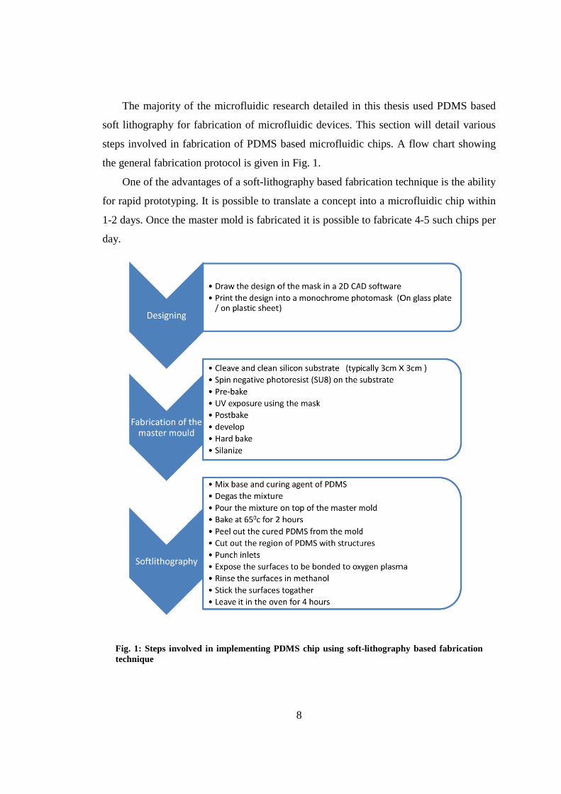
The majority of the microfluidic research detailed in this thesis used PDMS based
soft lithography for fabrication of microfluidic devices. This section will detail various
steps involved in fabrication of PDMS based microfluidic chips. A flow chart showing
the general fabrication protocol is given in Fig. 1.
One of the advantages of a soft-lithography based fabrication technique is the ability
for rapid prototyping. It is possible to translate a concept into a microfluidic chip within
1-2 days. Once the master mold is fabricated it is possible to fabricate 4-5 such chips per
day.
Fig. 1: Steps involved in implementing PDMS chip using soft-lithography based fabrication technique
9
2.3.1 Design of the mask
The first stage of the procedure is the design of the mask to be used for UV-
photolithography to fabricate the master mold. This is usually implemented using
suitable 2D Computer Aided Design (CAD) software. A commercial software package -
Elphy Plus (Raith) – was used for drawing the mask design. The drawn design can be
produced on glass masks if high resolution is needed or can be printed on flexible plastic
sheets (Microlithography services Ltd.), to obtain a monochrome photomask. Since
negative photoresist is used for fabricating the master mold, the region where structures
are to be retained are kept transparent in the photomask. While printing to plastic sheet is
cheaper compared to the glass masks, the resolution that can be achieved by this is
limited to ~20 µm, compared ~1 µm for the case of a glass mask.
2.3.2 Fabrication of the master mold
The next stage in the procedure is to fabricate the master mold which would be used
to mold the structure to a silicon elastomer. Hence to achieve microfluidic channels
which are the patterned relief structures on cured PDMS block, the master mold should
have raised structures defined in photoresist [11]. A negative photoresist – SU8
(Polymicro Inc.) – was used for defining the structures in the master mold. The master
mold was fabricated on a single side polished silicon wafer (IDB Technologies Ltd.).
The silicon wafer was cleaved to desired size (typically rectangles with sides between 2
cm – 4 cm) and was rinsed in acetone, isopropanol (IPA) and de-ionized water. After
drying with nitrogen, it is kept in an oven at a temperature of 180 0C for eight hours to
ensure that the surface of the substrate is fully dehydrated to maximize adhesion in the
next stage.
The next step was spinning SU8 on top of the substrate to get a flat layer of the
photoresist with the desired thickness. SU8 is a photoresist which allows formation of
relatively thick films (100s of micro-meters) by spinning. The thickness of the
photoresist can be controlled by adjusting the viscosity of the photoresist and rotation
speed of the spinner. There is a wide choice of photoresist with varying viscosities
available off the shelf. However it is also possible to create photoresist with intermediate
viscosity by mixing a highly viscous and low viscous SU8. SU8 2050 (high viscosity)
10
and SU8 2000.5 (low viscosity) were mixed in different ratios to produce photoresists
with the desired viscosity. The thickness of the spun photoresist is governed by the
empirical equation [13]:
2kp
tw
= [2.4]
Where, p is the resist solid content percentage, which is a function of viscosity of
the resist,w is the spinner speed in rpm/1000 and k is the spinner constant (typically 80-
100) that depends on various physical parameters such as the size of the wafer, the
humidity and the temperature of the environment. Although a calibration graph of
spinning speed vs. film thickness was given by the manufacturer for standard SU8 resists
with known viscosity, since the value of k is sensitive to the environment, calibration
was required for fabrication of each mold depending on the specific conditions.
For spinning the flat layer of SU8, first a drop of photoresist was poured on top of
the substrate, and by tilting the substrate the resist was allowed to flow and cover the
whole surface of the substrate. The spinning of the resist was performed in three steps. In
the first 15 seconds the substrate was spun at 500 revolutions per minute (rpm), which
ensures spreading of the resist evenly over the whole surface area of the substrate. In the
next 15 seconds the revolution speed would be increased to half of that of the final
spinning speed. This allowed removal of any extra SU8 from the substrate. In the final
stage the speed was increased to the actual desired speed and would spin for 30 s
spreading the SU8 layer evenly resulting in a flat layer of SU8 on the surface of the
silicon substrate. Although reducing the spinning speed would result in thicker films, it
is not desirable to reduce the spinning speed below 1000 rpm as this would create
unevenness of the final layer. For achieving higher thicknesses of the SU8 layer (~300
µm), a multi-layer spin coating of SU8 was possible by spinning multiple layers of SU8
after pre-baking each layer after spinning.
Once the spinning process was over, the layer had to be pre-baked (soft baked) on a
hot plate. This baking process was done at two temperatures. First the substrate was kept
for warming up at 65 0C and then the temperature would be ramped to 95 0C to complete
the baking process. The baking time varied depending on the thickness of the SU8 film
(typically for an 80 µm thick SU8 layer 5 minutes at 650C and 15 minutes at 95 0C).
11
After the pre-bake, the substrate was allowed to cool for 10 minutes prior to UV
exposure.
The next stage was UV photolithography, where the design on the printed mask is
transferred to the SU8 layer by UV exposure. Since SU8 is a negative photoresist, the
region which was exposed to UV would undergo a photochemical reaction resulting in
cross-linking (polymerization) of the material. The required exposure times depend upon
the thickness of the SU8 layer. While a low exposure time inhibits proper cross-linking,
a high exposure time would result in a trapezoidal channel cross section instead of a
rectangular one as the UV radiation leaks to the sides once the cross-linking process is
completed in the actual exposed region. When using low resolution printed mask for UV
photolithography, it is necessary to temporarily fix the mask onto a glass plate so as to
keep the mask flat during the exposure. To temporarily bond the mask to a glass plate a
drop of water was used as a bonding agent. A drop of water was placed onto a glass plate
and the mask was then placed on top of the water droplet, sandwiching a thin layer of
water between the glass substrate and the printed mask. The shear stress due to the
surface tension of the water provides a temporary but strong bond between the glass and
the printed mask. The UV exposure was performed on a mask aligner (Carl Zeiss) where
the substrate with SU8 layer was kept as close as possible to the mask to avoid leaking
of UV light through the edges of the mask during exposure.
Once UV exposure is complete the substrate was post-baked (post exposure baking)
to complete the cross-linking process of SU8. This baking step was performed similar to
that of pre-bake by warming up at 65 0C and then baking at 95 0C. The baking time is
dictated by the thickness of the material (typically 1 minute at 65 0C and 10 minutes at
95 0C for an SU8 layer of thickness 80 µm). After post-baking, the structures defined by
UV exposure would be visible on the substrate.
After post-baking stage, the substrate was allowed to cool down for 10 minutes prior
to development. The development is a two stage process where first the substrate would
be immersed in EC solvent (Microchem). Constant stirring of the developing solution is
required to ensure removal of the SU8 material that was not cross-linked. In order for
quick development it is possible to keep the substrate in EC solution in an ultra-sonic
bath. However it is not advisable for structures of height more than 50 µm, where
12
destruction of the structures may occur. Once the un-polymerised material was
completely dissolved in EC solution, the substrate would be rinsed in IPA and purged
with N2 gas for drying.
After completing the developing stage, the substrate was left in an oven at a
temperature 180 0C for 4 hours for hard baking. Any minor cracks in the structure after
developing would get fully cured during the hard baking procedure.
After the hard baking stage, the substrate was silanized to create a non-sticky layer
on top of the substrate which would ease pealing up of cured PDMS during the soft
lithography process. To silanize the substrate, trichlorosilane (Fluorochem) was
deposited on the substrate through vapor deposition using a desiccator. A drop of
trichlorosilane (~20 µl) was kept in the desiccator along with the substrate (keeping the
surface with the structure facing up). Using a vacuum pump, the gas inside the
desiccator was pumped out for 30 minutes, this causes the trichlorosilane to evaporate
and become deposited on the substrate. This stage completes the fabrication of mold.
The whole process of fabricating the master mold was performed in a class 10,000 clean
room facility.
2.3.3 Fabrication of PDMS chip using soft-lithography
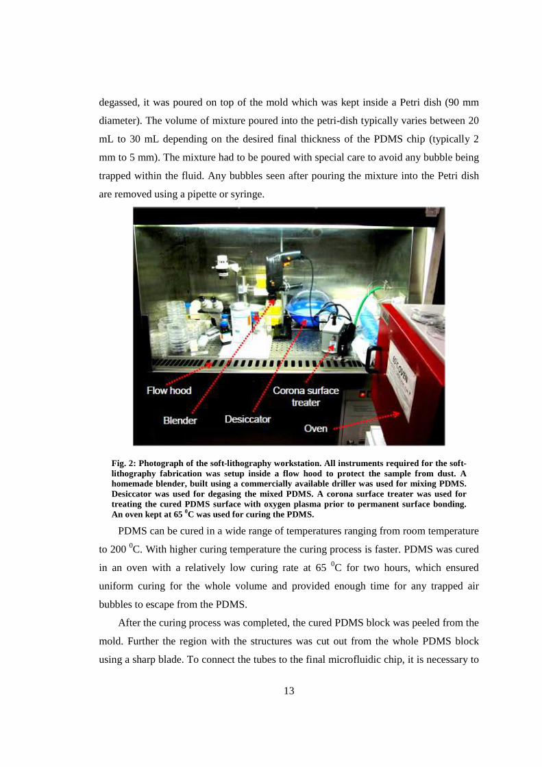
The next stage is to fabricate PDMS chips from the master mold using a stamping
and molding procedure. A soft-lithography workstation outside the cleanroom was used
for this stage of fabrication. The workstation as shown in Fig. 2 consists of a flow hood
containing facilities for preparing the PDMS mixture and processing the cured PDMS to
make the microfluidic chips. The workstation also has an oven kept at 65 0C to cure the
PDMS.
PDMS was prepared using a Sylgard 184 silicon elastomer kit (Dow Corning
Corporation) which comes in two parts, a base (clear and highly viscous) and a curing
agent (clear with low viscosity). The base and curing agent were mixed typically in the
ratio of 10:1 by weight (10:1.6 by volume), to prepare PDMS. This ratio can be tuned to
achieve a desired tensile strength for the cured PDMS (increasing the amount of curing
agent increases the tensile strength of the cured PDMS). After mixing the two parts of
PDMS, the mixture was degassed by keeping it in a desiccator. Once the mixture is
13
degassed, it was poured on top of the mold which was kept inside a Petri dish (90 mm
diameter). The volume of mixture poured into the petri-dish typically varies between 20
mL to 30 mL depending on the desired final thickness of the PDMS chip (typically 2
mm to 5 mm). The mixture had to be poured with special care to avoid any bubble being
trapped within the fluid. Any bubbles seen after pouring the mixture into the Petri dish
are removed using a pipette or syringe.
Fig. 2: Photograph of the soft-lithography workstation. All instruments required for the soft-lithography fabrication was setup inside a flow hood to protect the sample from dust. A homemade blender, built using a commercially available driller was used for mixing PDMS. Desiccator was used for degasing the mixed PDMS. A corona surface treater was used for treating the cured PDMS surface with oxygen plasma prior to permanent surface bonding. An oven kept at 65 0C was used for curing the PDMS.
PDMS can be cured in a wide range of temperatures ranging from room temperature
to 200 0C. With higher curing temperature the curing process is faster. PDMS was cured
in an oven with a relatively low curing rate at 65 0C for two hours, which ensured
uniform curing for the whole volume and provided enough time for any trapped air
bubbles to escape from the PDMS.
After the curing process was completed, the cured PDMS block was peeled from the
mold. Further the region with the structures was cut out from the whole PDMS block
using a sharp blade. To connect the tubes to the final microfluidic chip, it is necessary to
14
create inlet and outlet ports. These were punched using a micro-punch (Harris)
depending on the diameter of the tubing to be used for the microfluidic experiment
(typically 1.2 mm or 2 mm diameter). Typically the diameter of the inlet was kept
slightly below the diameter of the tube to be attached. Due to the elastic nature of the
PDMS material, this will allow insertion of the tubing into the inlets and would ensure
an automatic sealing which would be reversible.
The next stage is to bond the PDMS block with relief structures to a substrate,
which can be either a microscopic slide or a flat block of PDMS. There are mainly two
types of bonding possible, temporary and permanent. In temporary bonding, the surfaces
to be bonded were brought together and the Van der Waals force would hold them
together. Such bonds are suitable for experiments where the microfluidic flow was
achieved only through negative pressure created by suction. This type of bonding is
reversible. Permanent bonding is stronger and irreversible which could withstand
positive pressure inside the microfluidic channel. To achieve the permanent bonding, the
surfaces to be bonded were treated with oxygen plasma using a corona surface treater
(Electro Technic Products, Inc.) for 4 seconds each, which temporarily ionizes the
surfaces. The surfaces were then rinsed with methanol (Sigma Aldrich) and brought into
contact to be bonded. Rinsing with methanol allowed the surface to remain ionized for a
longer period of time, without this process the surfaces would be neutralized within one
minute after exposure to the oxygen plasma. Methanol acts as a lubricant, which helps to
slide one surface on top of another to position it properly. Methanol would evaporate
relatively quickly allowing the surfaces to bond. After bonding the two surfaces
together, the chip would be left inside a 65 0C oven for eight hours to ensure that the
surfaces are bonded properly. The chip would be ready to use after eight hours.
The fabrication protocol detailed in this section is the standard fabrication protocol
to fabricate a microfluidic chip containing microfluidic channels with rectangular cross
section. The protocol was modified to achieve a specialized channel cross section such
as circular, which will be discussed in later sections.
15
2.4 Embedding fiber into a PDMS microfluidic chip
Optical detection techniques have played a crucial role in the advancement of the
field of LoC [14]. However delivering and collecting optical signals in microfluidic
chips still remains as a challenge for which several solutions are being proposed by the
research community. One of these solutions is to develop LoC devices where all the
optical components such as source and detector are integrated into the microfluidic chip
[15]. Another approach is to use integrated [16] or embedded [17] waveguides to create
optical paths to microfluidic chips.
The latter approach is often realized by embedding an optical fiber into pre-defined
fiber insertion channels. The realization of such pre-defined fiber insertion channels
using soft-lithography based fabrication techniques is not trivial, as the shape of the
microfluidic channel that can be fabricated is limited only to a rectangular cross section
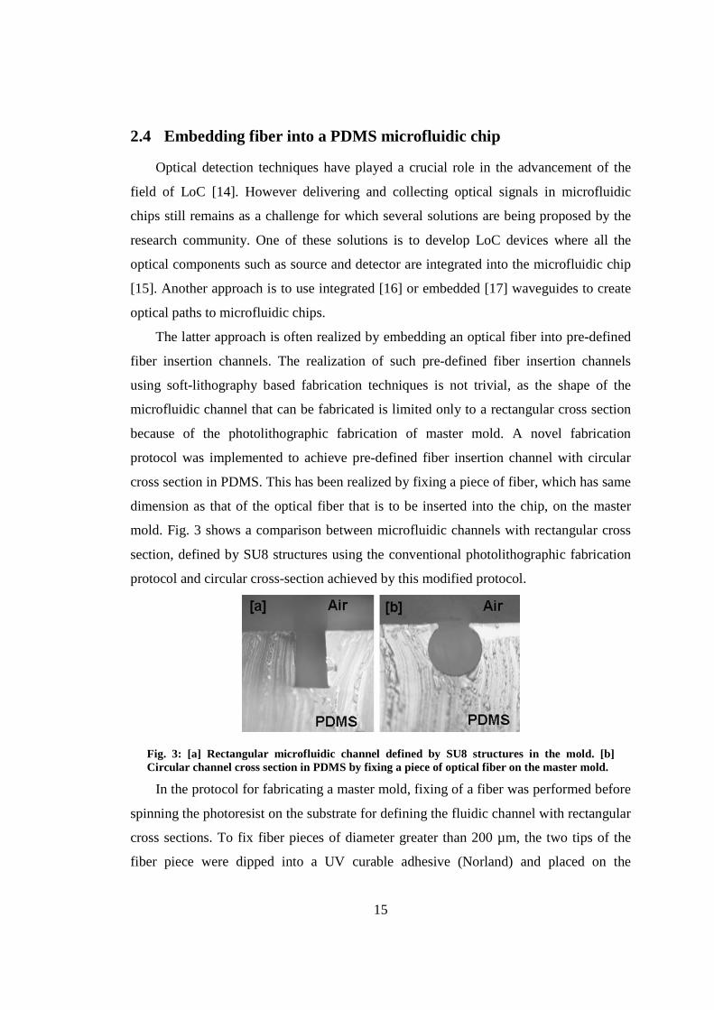
because of the photolithographic fabrication of master mold. A novel fabrication
protocol was implemented to achieve pre-defined fiber insertion channel with circular
cross section in PDMS. This has been realized by fixing a piece of fiber, which has same
dimension as that of the optical fiber that is to be inserted into the chip, on the master
mold. Fig. 3 shows a comparison between microfluidic channels with rectangular cross
section, defined by SU8 structures using the conventional photolithographic fabrication
protocol and circular cross-section achieved by this modified protocol.
Fig. 3: [a] Rectangular microfluidic channel defined by SU8 structures in the mold. [b] Circular channel cross section in PDMS by fixing a piece of optical fiber on the master mold.
In the protocol for fabricating a master mold, fixing of a fiber was performed before
spinning the photoresist on the substrate for defining the fluidic channel with rectangular
cross sections. To fix fiber pieces of diameter greater than 200 µm, the two tips of the
fiber piece were dipped into a UV curable adhesive (Norland) and placed on the
16
substrate. Subsequently the substrate was exposed to UV to cure the adhesive which
would hold the piece of fiber to the substrate. However this approach would not be
sufficient to fix fibers whose diameter is ~125 µm (diameter of standard single mode
fibers). Adhesive just on the end would not be sufficient to hold fibers of this dimension.
Also during the process of pealing PDMS from the mold, this will leave some PDMS
lips on the fluidic channel. Hence to fix fibers of smaller diameter, SU8 was used as
adhesive. A 5 µm thick SU8 was spun on top of the silicon substrate. The fiber to be
fixed was dropped on top of the thin SU8 layer. After pre-baking, the whole SU8 layer
was flood exposed leaving a flat SU8 layer with the fiber stuck on this layer. The
standard protocol was then followed to define other microfluidic channels on this
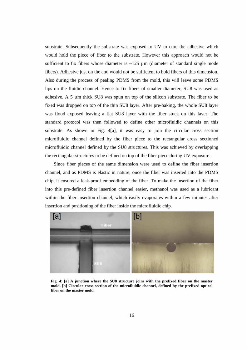
substrate. As shown in Fig. 4[a], it was easy to join the circular cross section
microfluidic channel defined by the fiber piece to the rectangular cross sectioned
microfluidic channel defined by the SU8 structures. This was achieved by overlapping
the rectangular structures to be defined on top of the fiber piece during UV exposure.
Since fiber pieces of the same dimension were used to define the fiber insertion
channel, and as PDMS is elastic in nature, once the fiber was inserted into the PDMS
chip, it ensured a leak-proof embedding of the fiber. To make the insertion of the fiber
into this pre-defined fiber insertion channel easier, methanol was used as a lubricant
within the fiber insertion channel, which easily evaporates within a few minutes after
insertion and positioning of the fiber inside the microfluidic chip.
Fig. 4: [a] A junction where the SU8 structure joins with the prefixed fiber on the master mold. [b] Circular cross section of the microfluidic channel, defined by the prefixed optical fiber on the master mold.
17
2.5 PDMS membrane based microfluidic fabrication
The soft-lithography based PDMS fabrication protocol detailed in section 2.3.3 is
for fabricating microfluidic channels within PDMS blocks. For some specific
applications such as implementation of microvalves mentioned in section 2.7 [18],
membrane based PDMS fabrication would be desirable. Depending on the applications,
PDMS membrane thicknesses can vary from 50 µm to 1 mm. The fabrication protocol
varies depending on the desired thickness of the membrane.
To fabricate membranes with relatively low thickness (~50 µm), uncured PDMS
was spun onto a flat glass or silicon substrate which had previously been silanized. The
curing process was performed on a hotplate at 120 0C for 3 to 5 minutes. Once PDMS
was cured, the membrane was carefully peeled out.
If a relatively thick (~800 µm to 1 mm) membrane was required and the actual
specific thickness is not a concern, uncured PDMS was allowed to spread on a silanized
flat substrate followed by a quick curing on a hotplate as mentioned in the previous
method. To control the thickness of the membrane, uncured PDMS was sandwiched
between two silanized substrates, keeping a spacer of desired thickness between the
substrates. This ensured PDMS membrane which is flat on both sides and has a known
thickness.
2.6 Microfluidic channels with optical windows on both sides
Optical access to microfluidic channels is always a major concern when designing
optofluidic chips. When implementing techniques such as optical tweezers, which uses a
high numerical aperture objective, within optofluidics, it is desirable to have an optically
flat window of thickness ~100 µm to avoid aberrations on the optical beam delivered
into the microfluidic channel. This is usually achieved by using a microscope coverslip
as the substrate in the bottom of a PDMS microfluidic chip.
For some specific applications it is necessary to have similar optical window on
both sides of the microfluidic channels (top and bottom). For example, to implement
Digital Holographic Microscopy (DHM) in transmission mode [19], optical windows on
both sides of the microfluidic channel are desirable. The conventional soft-lithography
protocol does not allow this as on top of the channel there would be PDMS material.
18
Even if the channel was fabricated using a PDMS membrane, to reduce the thickness of
the material on top of the channel, the membrane would not be optically flat, leading to
unnecessary aberrations.
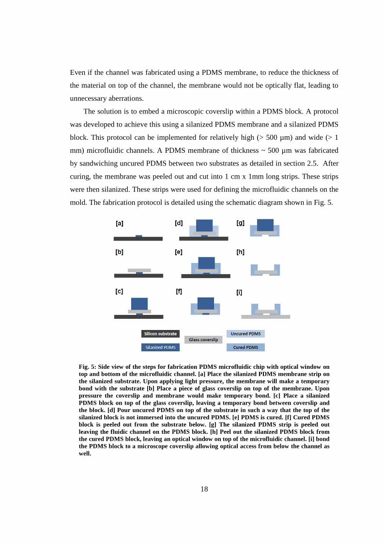
The solution is to embed a microscopic coverslip within a PDMS block. A protocol
was developed to achieve this using a silanized PDMS membrane and a silanized PDMS
block. This protocol can be implemented for relatively high (> 500 µm) and wide (> 1
mm) microfluidic channels. A PDMS membrane of thickness ~ 500 µm was fabricated
by sandwiching uncured PDMS between two substrates as detailed in section 2.5. After
curing, the membrane was peeled out and cut into 1 cm x 1mm long strips. These strips
were then silanized. These strips were used for defining the microfluidic channels on the
mold. The fabrication protocol is detailed using the schematic diagram shown in Fig. 5.
Fig. 5: Side view of the steps for fabrication PDMS microfluidic chip with optical window on top and bottom of the microfluidic channel. [a] Place the silanized PDMS membrane strip on the silanized substrate. Upon applying light pressure, the membrane will make a temporary bond with the substrate [b] Place a piece of glass coverslip on top of the membrane. Upon pressure the coverslip and membrane would make temporary bond. [c] Place a silanized PDMS block on top of the glass coverslip, leaving a temporary bond between coverslip and the block. [d] Pour uncured PDMS on top of the substrate in such a way that the top of the silanized block is not immersed into the uncured PDMS. [e] PDMS is cured. [f] Cured PDMS block is peeled out from the substrate below. [g] The silanized PDMS strip is peeled out leaving the fluidic channel on the PDMS block. [h] Peel out the silanized PDMS block from the cured PDMS block, leaving an optical window on top of the microfluidic channel. [i] bond the PDMS block to a microscope coverslip allowing optical access from below the channel as well.
19
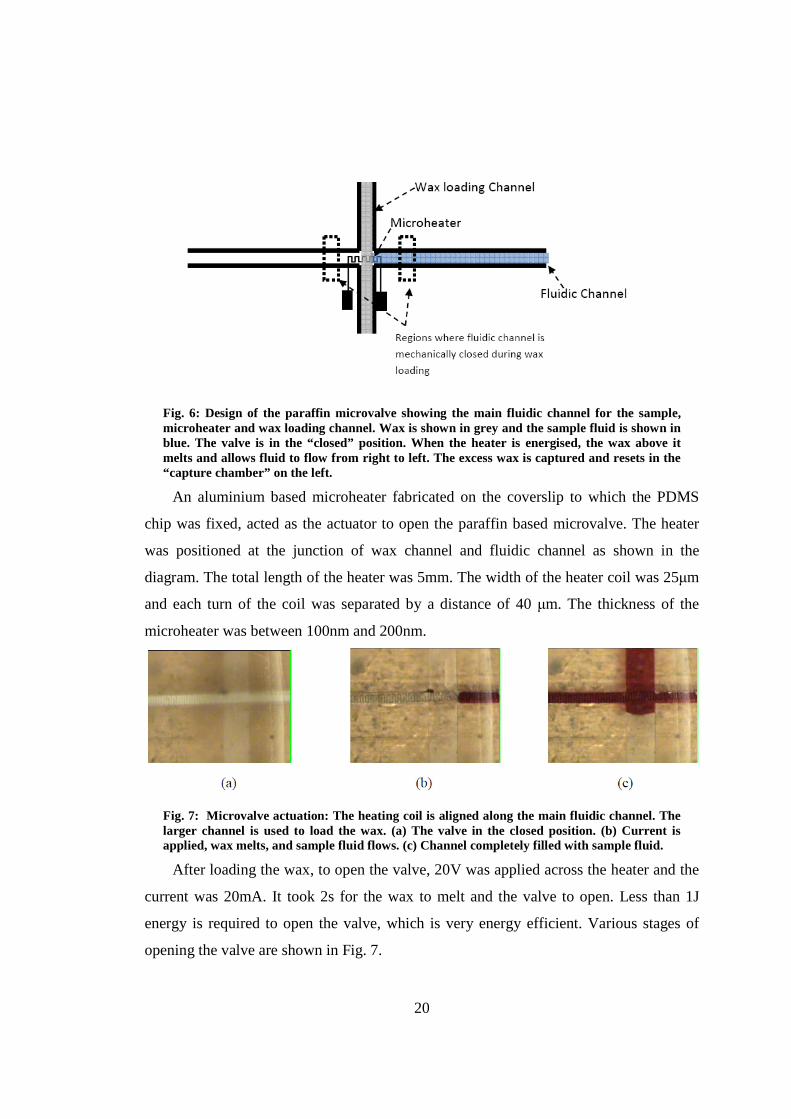
2.7 Paraffin microvalve
Every microfluidic based sensor system requires a microvalve for controlled sample
input. There are mainly two types of microvalve approaches – Active and Passive
[20,21]. Passive microvalves generally act as a check valve to restrict the flow only in
one direction, whereas active microvalves involve actuators for the valve operation. A
simple paraffin based active microvalve was designed for a one time use sensor. In this
case since the sensor is for one time use only, the valve required should be a single shot
close-open valve. The final device had to be portable, hence the power consumption to
open the valve should be kept as minimum as possible. Also the valve has to be
compatible with PDMS based soft lithographic fabrication techniques.
Thermally actuated non-mechanical microvalves based on phase changing nature of
paraffin wax have proved to be ideal for a low response time for opening which will
result in less power consumption [22,23]. Also paraffin based microvalves tend to hold
higher pressure compared to its closest counterparts [21]. In contrast to the work of Liu
et al. [23], where the channel size was in the range of millimeters, the size of the channel
for the chip used in this study was 250x50µm. This small dimension makes it difficult to
load the wax into the channel to close the valve.
The microvalve was fabricated in a single layered PDMS membrane of thickness
~800µm, using conventional soft lithographic techniques [7]. To load the wax a wax
loading channel crossing perpendicular to the fluidic channel was used as shown in Fig.
6.
The paraffin wax used in this work had a melting point at 470C. To load the wax,
the whole chip was heated to a temperature of 800C using Peltier heater and a block of
solid paraffin wax was kept at one end of the wax loading channel. The molten wax was
drawn into the wax loading channel due to capillary action which formed a solid plug
upon cooling. To avoid wax flowing through the main fluidic channel during loading,
the wax channel was temporarily isolated from the rest of the device by applying
mechanical pressure over the membrane as indicated in Fig. 6.
20
Fig. 6: Design of the paraffin microvalve showing the main fluidic channel for the sample, microheater and wax loading channel. Wax is shown in grey and the sample fluid is shown in blue. The valve is in the “closed” position. When the heater is energised, the wax above it melts and allows fluid to flow from right to left. The excess wax is captured and resets in the “capture chamber” on the left.
An aluminium based microheater fabricated on the coverslip to which the PDMS
chip was fixed, acted as the actuator to open the paraffin based microvalve. The heater
was positioned at the junction of wax channel and fluidic channel as shown in the
diagram. The total length of the heater was 5mm. The width of the heater coil was 25µm
and each turn of the coil was separated by a distance of 40 µm. The thickness of the
microheater was between 100nm and 200nm.
Fig. 7: Microvalve actuation: The heating coil is aligned along the main fluidic channel. The larger channel is used to load the wax. (a) The valve in the closed position. (b) Current is applied, wax melts, and sample fluid flows. (c) Channel completely filled with sample fluid.
After loading the wax, to open the valve, 20V was applied across the heater and the
current was 20mA. It took 2s for the wax to melt and the valve to open. Less than 1J
energy is required to open the valve, which is very energy efficient. Various stages of
opening the valve are shown in Fig. 7.
21
2.8 Conclusion
This chapter details the background of the theory of microfluidics and basic
fabrication techniques, which have been used for the research detailed in the following
chapters. The soft lithography based fabrication protocol explained in 2.3 is the standard
one. One of the focal points of the studies presented in this thesis is the means by which
various optical techniques were incorporated into microfluidics to achieve optofluidic
devices with enhanced functionalities and portability. This required modification of the
standard soft-lithography protocols to achieve specialized functions. One of such
modifications was to achieve pre-defined fiber insertion channels with circular cross-
sections in PDMS. The technique where a fiber piece was incorporated into the master
mold to achieve such a fiber insertion channel played a crucial role in developing
various optofluidic devices for optical sorting and chemical sensing which are detailed in
following chapters.
When designing microfluidic chips, to be integrated with free-space imaging
devices such as biological microscopes, an important design consideration is to provide
proper optical windows to probe the sample inside the microfluidic channel without the
substrate causing optical aberrations. Conventional soft-lithographic techniques offer a
means to provide such an optical window on one side of the channel by bonding the
PDMS block to a microscope coverslip. However for some specific applications such as
DHM based imaging of a sample in a microfluidic channel, optical access on two sides
of the microfluidic channel may be necessary. This was achieved by a modified protocol
using silanized PDMS membranes and PDMS blocks.
One of the design constraints when implementing a microfluidic sensor is the
implementation of micro-valves for controlling the flow within the microfluidic channel.
Depending on the application, there are various design parameters to be taken into
consideration while designing such a valve, such as ease to incorporate into the current
fabrication protocol, ease of actuation, amount of pressure it can withstand and size. This
chapter also discussed the implementation of a paraffin based close-open microvalves
which were designed for heat actuated activation. This microvalve was designed with an
option to easily multiplex within a microfluidic chip as this was designed for a
22
microfluidic sensor where multiple sensors would be embedded within one microfluidic
chip.
Although a general overview of the fabrication protocol was presented in this
chapter, modifications to this were used in designing and implementing various devices
discussed in the following chapters. The specific fabrication protocol used for each
project is explained in detail in respective chapters in later parts of this thesis.
Relevant publications
• Dharanipathy UP, Di Falco A, Scullion MG, Ashok PC, Marchington RF,
Krauss TF (2009) An integrated slotted photonic crystal biosensor array.
Paper presented at the EOS Topical Meeting on "Blue" Photonics - Optics in
the Sea Aberdeen,
• James TD, Scullion MG, Ashok PC, Di Falco A, Dholakia K, Krauss TF
(2011) Valve controlled fluorescence detection system for remote sensing
applications. Microfluidics and Nanofluidics:1-8. doi:10.1007/s10404-011-
0818-1
Contributions
The protocol detailed in section 2.6 was conceived and implemented by P. C.
Ashok. In the work mentioned in section 2.7, P. C. Ashok initiated the work on
fabricating paraffin based microvalves and proposed the idea of using a cross
microfluidic channel for loading paraffin wax. M. G. Scullion fabricated the prototype
valve and performed initial testing with the assistance of P. C. Ashok.
23
3. Integrated optical chromatography using photonic crystal fiber
3.1 Introduction
Optical chromatography is a simple and promising passive sorting technique, which
utilizes the interplay between microfluidic drag force and the optical radiation force to
achieve spatial separation of microparticles. When a particle in a microfluidic flow
encounters a gently focused laser beam propagating coaxially in the opposite direction to
the flow, the particle experiences a force against the flow due to the radiation pressure of
the laser beam. The particle comes to a rest point where the optical forces are balanced
by the Stokes’ viscous drag force. The distance of the rest point from the focus of the
laser beam is referred to as the retention distance. The retention distance of the particle is
dependent upon the size, refractive index and shape of the particle for a fixed laser beam
power and fluid flow velocity which is explained mathematically in [24]. Optical
chromatography has been applied to the separation of colloidal materials and to
different species of biological particles [25]. Optical chromatography has also been used
to study the in situ reaction rates in immunoassays [26]. The field of optical
chromatography is maturing with the capability for filtering out, concentrating and
collecting a particular species from a mixture of particles for analysis [27].
The major limitations for the application of optical chromatography are the
necessity for highly stable fluid flow and the intricate alignment of laser beam required
with respect to the chromatography channel [28]. Despite developments in the fluid
delivery platforms of optical chromatography systems [5, 6], there have been no
integrated approaches for launching the laser beam into the chromatography chip to date.
Coupling of the laser into the fluid channel is typically achieved by free space alignment
methods, which requires specialist expertise for every single run of the experiment [29] ,
limiting the application of this technology.
The works presented in this chapter, takes a step towards integration by achieving
on-chip delivery of a laser beam for chromatography using Photonic Crystal Fiber.
Choosing the most appropriate waveguide for light delivery and design of the chip are
the key factors for achieving this result. A schematic of the chip is shown in Fig. 8,
which is fabricated using soft lithography. The major feature of this chip is the use of
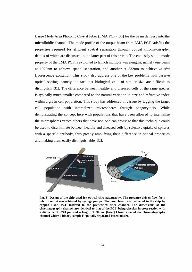
24
Large Mode Area Photonic Crystal Fiber (LMA PCF) [30] for the beam delivery into the
microfluidic channel. The mode profile of the output beam from LMA PCF satisfies the
properties required for efficient spatial separation through optical chromatography,
details of which are discussed in the latter part of this article. The endlessly single mode
property of the LMA PCF is exploited to launch multiple wavelengths, namely one beam
at 1070nm to achieve spatial separation, and another at 532nm to achieve in situ
fluorescence excitation. This study also address one of the key problems with passive
optical sorting, namely the fact that biological cells of similar size are difficult to
distinguish [31]. The difference between healthy and diseased cells of the same species
is typically much smaller compared to the natural variation in size and refractive index
within a given cell population. This study has addressed this issue by tagging the target
cell population with internalized microspheres through phagocytocis. While
demonstrating the concept here with populations that have been allowed to internalize
the microspheres verses others that have not, one can envisage that this technique could
be used to discriminate between healthy and diseased cells by selective uptake of spheres
with a specific antibody, thus greatly amplifying their difference in optical properties
and making them easily distinguishable [32].
Fig. 8: Design of the chip used for optical chromatography. The pressure driven flow from inlet to outlet was achieved by syringe pumps. The laser beam was delivered to the chip by capped LMA PCF inserted to the predefined fiber channel. The dimensions of the chromatography channel are identical to that of the PCF, being circular in cross section with a diameter of ~240 µm and a length of 20mm. [Inset] Closer view of the chromatography channel where a binary sample is spatially separated based on size.
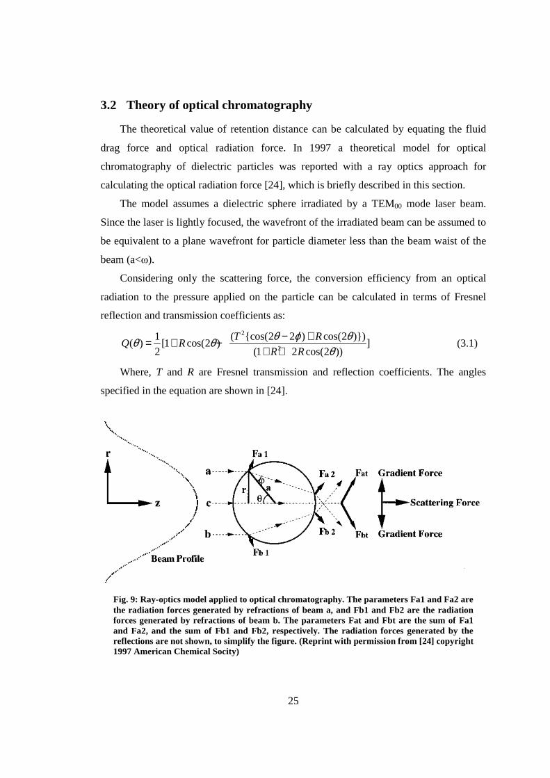
25
3.2 Theory of optical chromatography
The theoretical value of retention distance can be calculated by equating the fluid
drag force and optical radiation force. In 1997 a theoretical model for optical
chromatography of dielectric particles was reported with a ray optics approach for
calculating the optical radiation force [24], which is briefly described in this section.
The model assumes a dielectric sphere irradiated by a TEM00 mode laser beam.
Since the laser is lightly focused, the wavefront of the irradiated beam can be assumed to
be equivalent to a plane wavefront for particle diameter less than the beam waist of the
beam (a<ω).
Considering only the scattering force, the conversion efficiency from an optical
radiation to the pressure applied on the particle can be calculated in terms of Fresnel
reflection and transmission coefficients as:
2
2
1 ( (2 2cos ) cos(2 ))( ) [1 cos(2 ) ]
2 (1 2 cos(2 ))
T RQ R
R R
θ ϕ θθ θθ
− += + −+ +
(3.1)
Where, T and R are Fresnel transmission and reflection coefficients. The angles
specified in the equation are shown in [24].
Fig. 9: Ray-optics model applied to optical chromatography. The parameters Fa1 and Fa2 are the radiation forces generated by refractions of beam a, and Fb1 and Fb2 are the radiation forces generated by refractions of beam b. The parameters Fat and Fbt are the sum of Fa1 and Fa2, and the sum of Fb1 and Fb2, respectively. The radiation forces generated by the reflections are not shown, to simplify the figure. (Reprint with permission from [24] copyright 1997 American Chemical Socity)

26
2 2
2 2
1 sin ( ) tan ( )
2 sin ( ) tan ( )R
θ ϕ θ ϕθ ϕ θ ϕ
− −= + + + (3.2)
2 2 2
1 sin 2( )sin( ) sin 2( )sin( )
2 sin ( ) sin ( )cos ( )T
θ ϕ θ ϕθ ϕ θ ϕ θ ϕ
= + + + − (3.3)
If n1 and n2 are the refractive indices of the surrounding medium and particle, the
angles θ and are related by Snell’s law as:
( )1 2sin sin( )n nθ ϕ= (3.4)
The radiation force as a function of incident angle is given by
( ) ( ) 1n PF Q
cθ θ= (3.5)
( ) ( ) 1n dPdF Q
cθ θ= (3.6)
Where, dP is the power of the incident beam on a small area of the particle
The intensity of the laser beam varies in transverse direction as:
2
2
2
0
r
I I e ω
− = (3.7)
Where I0 is the intensity at the beam center and ω is the beam waist of the Gaussian
beam.
( )a sinr θ= (3.8)
Hence
2 2
0 2
2 sin ( )exp
aI I
θω
=
(3.9)
( )2 2
20 2
2 ( )2 sin 2 exp
a sindP rdr I a I d
θπ π θ θω
= =
(3.10)
Substituting dP in equation (3.6) and assuming2
1a
ω <<
, total force due to
radiation pressure on the particle can be evaluated as:

27
2*12
R
n P aF Q
c ω =
(3.11)
Where,
( ) ( )2
*
0
sin 2 Q Q dπ
θ θ θ= ∫ (3.12)
For Gaussian beams,
2
2 20 1
c
z
zω ω
= +
(3.13)
Where cz is the Rayleigh range given by
21 0
c
nz
πωλ
= (3.14)
The force on the particle due to fluid flow can be expressed using Stokes law for a
particle moving with a velocity v as:
6fF avπη= (3.15)
Where, η is the viscosity of the medium, where the particle is suspended.
The expression for retention distance z can be calculated by equation FR and Ff as:
2 *1 0 1
20
13
n n PQ az
vc
πωλ πη ω
= − (3.16)
From the equation it is clear that retention distance depends on the radius of the
particle and refractive index of the particle. Larger particles will have larger retention
distance also higher refractive index particles will also have a larger retention distance.
The retention distance can be adjusted by changing the fluid flow rate or the power of
the laser beam.
3.3 History of optical chromatography
As first reported by T. Imasaka et al. in 1995 [33], optical chromatography was
demonstrated to be capable of fractionating dielectric particles by size. In this
experiment a dielectric particle was introduced into a capillary tube by a laminar liquid
28
flow. A lightly focused counter-propagating free-space laser beam was aligned parallel
to this fluid flow. The optical gradient forces trapped the particle along the center of the
laser beam and accelerated it against the fluid flow, away from the beam waist due to the
radiation pressure. Counter to this, the Stokes fluid drag force decelerated the particle
until finding an equilibrium position where the fluid drag force and radiation force
balanced. The distance between the equilibrium position and the beam waist was termed
the retention distance. The value of the retention distance was found to be dependent
upon the size of the particle, and later also the refractive index [34] and hydrodynamic
profile (predominantly shape) of the particle [29]. The retention distance is also a
function of the laser power and fluid flow rate. It was in this first paper that the
technique was termed optical chromatography due to its ability to obtain classical
chromatography-like separations of various species of samples.
In a second paper from the same group [24], the analogies between their new
technique and the conventional equivalent were extended through the development of a
theoretical model, which until recently has underpinned all experimental work in the
field. A ray optics approach was applied to the particle-light field interaction for a
propagating Gaussian beam, and balanced by the Stokes fluid drag force. From this
various parameters were obtainable, as functions of particle size and refractive index,
which were directly analogous to those in classical chromatography. The retention
distance (as opposed to retention time), selectivity, theoretical plate number, and
resolution were calculated as a function of the laser power, flow rate, particle size and
refractive index. The technique was compared to other separation techniques, such as
field flow fractionation, gas and liquid chromatography, and size exclusion
chromatography.
The same paper also demonstrated the first biological application of optical
chromatography, where it was shown that human erythrocytes could be successfully split
into two sub-populations using the technique. The potential of optical chromatography
as a biological tool was thoroughly embedded through another paper by the group,
where the technique was applied to immunoassay of protein [26]. Polymer beads coated
by an appropriate antibody (anti-mouse IgG) were flowed into the optical
chromatography setup and the retention distance was observed. A concentration of
29
antigen (mouse IgG) was then introduced in, generating bead-bead binding through the
presence of the antigen. Bound coagulated beads exhibit an increased radiation pressure
thus receiving an increase in retention distance by up to 500 µm compared to the
unbound free beads. The ratio of free to bound beads was calculated, providing a
reaction probability and protein concentration of the order of 10 ng/mL could be
measured. The reversibility of the reaction in real time was also investigated by
monitoring the exchange to and from the bound and unbound beads as visualized on a
camera. As such, optical chromatography provided the capability to study for the first
time a single bond reversible reaction, as well as the capacity to watch the reaction in
real time. A follow-up paper [35] improved the sensitivity of the experiment down to
1ng/mL by altering the bead size, and provided an investigation into the role of antigen
concentration in dissociation.
As well as supplying a means of separating particles according to retention distances
dependent upon particle properties, optical chromatography has branched into three not
so dissimilar approaches, namely the optical funnel, the optical channel and the optical
chromatography filter. The various names are more of an indication of a different
application rather than a change in experimental setup. The optical funnel is a technique
for measuring the force a biological particle can exert to escape the gradient forces of the
optical field within an optical chromatography setup. This was first applied to fresh
water bacteria Trachelomonas volvocina [36] and later to sperm cells [37] and allowed
large numbers (100’s) of cells to be characterized in a few hours.
The optical channel is another variation on the optical chromatography for
measuring the elasticity of a cell. In contrast to the work on the optical stretcher [38],
here the fluid flow gives rise to the stretch of a trapped cell, rather than the optical field.
Briefly, a flow of cells is flowed against a lightly diverging optical beam, which traps
cells on axis. The cell is allowed to flow through the beam focus, at which point it
elongates in one direction due to the fluid shear stresses, and the elongation is measured
from a CCD image giving a one dimensional shear strength measurement of the cell.
Here, erythrocyte shear strength was measured as a function of the age of the cell.
The most recent variation on optical chromatography is the optical filter. The first
paper on optical chromatography published by the group which developed “optical

30
chromatographic flter”, demonstrated sorting of microscopic particles based on
refractive index contrast [34]. Separations of several hundred of microns were exhibited
for a poly-disperse sample of silica, PMMA and polystyrene spheres. This was followed
by the exciting report of the separation of the etiological agent of the mammalian disease
anthrax, Bacillus anthracis bacteria, from both its spore and from the common
environmental interferents, pollen. The separation of mulberry and ragweed pollen was
also demonstrated. The publication was of utmost interest to the biodefense area as B.
Anthracis is a common biological warfare threat. In another publication a distinct optical
chromatographic separation between B. Anthracis and its close relative B. Thuringiensis
based on subtle differences in their morphologies was reported [29]. On close inspection,
Bacillus Thuringiensis was observed to be more of an oblate spheroid in shape and also
exhibited a larger exosporium, giving rise to changes in both the hydrodynamic and
optical forces involved.
The same group used custom PDMS chips with varying channel dimensions to
enhance the optical chromatography separations, demonstrated on colloidal particles and
spores of B. Anthracis and Mulberry pollen [39]. The focusing lens was adjusted to
move the beam waist and position the separation such that the two types of particles
were collected either side of a point where the channel width increased rapidly. The
linear fluid flow is slower in a wider channel, resulting in a reduced Stokes fluid force
and an increased retention distance compared to that in the narrower flow channel
region. As a result, the retention distance of one species can be artificially increased to
accentuate an already present difference in retention between two species.
Hart et. al. later reported a new chip design and application that they termed an
optical chromatographic filter [40]. Here, instead of holding two or more species at
different retention distances, the laser and flow parameters are altered such that one
species is held up and the others are allowed to flow through. The channel is made
narrower and shorter, and the beam fills the entire channel ensuring that all particles feel
the optical force. These adjustments evade the common issues with previous designs,
where only a small fraction of particles are trapped by the beam and allows for a large
number to be held up without producing instabilities in the equilibrium positions due to
rescattering of the beam due to the particles. The new setup allows for separations of
31
particles, or as demonstrated with B. Anthracis, a sample can be bio-enriched to produce
a more concentrated pure sample. The technique represents a more robust experimental
setup, capable of dealing with much higher number of particles, as demonstrated in their
later publication where separation efficiencies of 99% were achieved for thousands of
polymer and silica particles compared to tens of particles in previous setups [41]. The
particle trajectories in an optical chromatography filter setup has also been modeled [42],
using a finite element method for solving the Navier-Stokes equations and a ray optics
model for the optical field.
While the previously mentioned research gives an overview of the development of
the field of optical chromatography, there were proposals for variant of the same
concepts. One group developed a theoretical model for cross type optical
chromatography [43] where, unlike in conventional optical chromatography the laser
beam would be aligned orthogonal to the flow direction. This idea utilizes the parabolic
flow velocity profile in the microfluidic channel to achieve separation.
Another recent study reported an optical chromatography like system where the
hollow core of a liquid filled photonic band-gap fiber was used as fluidic channel [44].
The photonic band-gap fiber was specially designed in such a way that the laser beam
for retaining the particles in the channel against flow could be coupled as a single mode
into the hollow core of the fiber. The authors claimed that this device has ability to
precisely control the retention distance of the particle by manipulating the power of the
laser beam and flow speed inside the core of the fiber.
3.4 Optical Chromatography with on-chip light delivery – Rationale
As mentioned previously one of the limitations of the previous embodiments of an
optical chromatographic system was its alignment requirements. To obtain optical
chromatographic fractionation, the alignment of the fractionation beam should be coaxial
to the fluid flow direction. Often there needs to be an added stage of procedure where
colloidal particles with known size and refractive index was flown through the
microfluidic chip and held at retention region to verify the coaxial alignment of optical
beam with respect to the flow direction [28,27]. Repeating this procedure before each
32
run makes the method time consuming and optical alignment expertise is essential to run
these experiments.
A solution to this would be to deliver the optical beam into the chip through a
waveguide such as an optical fiber, where the optical fiber could be inserted into the
microfluidic chip through a pre-defined fiber insertion channel. This would avoid any
requirement for special expertise in optical alignment. The motivation of this study is to
implement a microfluidic device where optical chromatography can be performed with
optical beam delivered on- chip
3.5 Design of optical chromatography chip with on-chip fiber light delivery
3.5.1 Choice of the fiber – Large Mode Area Photonic Crystal Fiber (LMA-PCF)
The key design parameter for an integrated light delivery approach is the choice of
optical fiber that achieves a beam with a good TEM00 mode profile and a low
divergence. To get TEM00 mode output, a single mode fiber needs to be used. The
numerical aperture (NA) of standard single mode fiber is comparatively high, (~0.13 for
fibers at λ=1070nm operational range) which results in high divergence of the output
beam. The use of LMA PCF addresses this issue, as its NA is only ~0.055 for a laser of
wavelength 1070nm. One of the limitations of a standard single mode fiber based
delivery system is that only a narrow bandwidth of wavelengths may typically be
delivered through the fiber. However the right choice of endlessly single mode LMA
PCF enables us to introduce multiple wavelengths to the chip through the same fiber
simultaneously. Two LMA PCFs of similar performance characteristics were used for
this experiment, LMA – 25 and LMA - 20 PCFs (NKT Photonics). The cladding of this
particular fiber consists of a photonic crystal structure with hexagonal symmetry and a
solid core, as shown in Fig. 10a. Even though the NA of LMA – 25 is slightly lower
(<0.001) than that of LMA 20, the insertion loss for 532nm laser is higher for LMA – 25
compared to LMA – 20. Therefore, for most of the experiments, LMA – 20 was used as
it presents the best compromise for operation at multiple wavelengths.
The output mode of LMA PCF is hexagonal as shown in Fig. 10b. In the close
vicinity of the apex of the fiber, the beam first comes to a focus at 150µm, before slowly
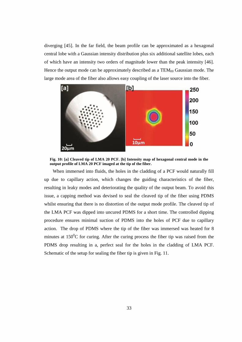
33
diverging [45]. In the far field, the beam profile can be approximated as a hexagonal
central lobe with a Gaussian intensity distribution plus six additional satellite lobes, each
of which have an intensity two orders of magnitude lower than the peak intensity [46].
Hence the output mode can be approximately described as a TEM00 Gaussian mode. The
large mode area of the fiber also allows easy coupling of the laser source into the fiber.
Fig. 10: [a] Cleaved tip of LMA 20 PCF. [b] Intensity map of hexagonal central mode in the output profile of LMA 20 PCF imaged at the tip of the fiber.
When immersed into fluids, the holes in the cladding of a PCF would naturally fill
up due to capillary action, which changes the guiding characteristics of the fiber,
resulting in leaky modes and deteriorating the quality of the output beam. To avoid this
issue, a capping method was devised to seal the cleaved tip of the fiber using PDMS
whilst ensuring that there is no distortion of the output mode profile. The cleaved tip of
the LMA PCF was dipped into uncured PDMS for a short time. The controlled dipping
procedure ensures minimal suction of PDMS into the holes of PCF due to capillary
action. The drop of PDMS where the tip of the fiber was immersed was heated for 8
minutes at 1500C for curing. After the curing process the fiber tip was raised from the
PDMS drop resulting in a, perfect seal for the holes in the cladding of LMA PCF.
Schematic of the setup for sealing the fiber tip is given in Fig. 11.
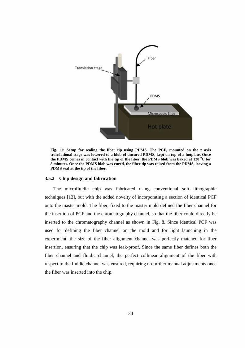
34
Fig. 11: Setup for sealing the fiber tip using PDMS. The PCF, mounted on the z axis translational stage was lowered to a blob of uncured PDMS, kept on top of a hotplate. Once the PDMS comes in contact with the tip of the fiber, the PDMS blob was baked at 120 0C for 8 minutes. Once the PDMS blob was cured, the fiber tip was raised from the PDMS, leaving a PDMS seal at the tip of the fiber.
3.5.2 Chip design and fabrication
The microfluidic chip was fabricated using conventional soft lithographic
techniques [12], but with the added novelty of incorporating a section of identical PCF
onto the master mold. The fiber, fixed to the master mold defined the fiber channel for
the insertion of PCF and the chromatography channel, so that the fiber could directly be
inserted to the chromatography channel as shown in Fig. 8. Since identical PCF was
used for defining the fiber channel on the mold and for light launching in the
experiment, the size of the fiber alignment channel was perfectly matched for fiber
insertion, ensuring that the chip was leak-proof. Since the same fiber defines both the
fiber channel and fluidic channel, the perfect collinear alignment of the fiber with
respect to the fluidic channel was ensured, requiring no further manual adjustments once
the fiber was inserted into the chip.
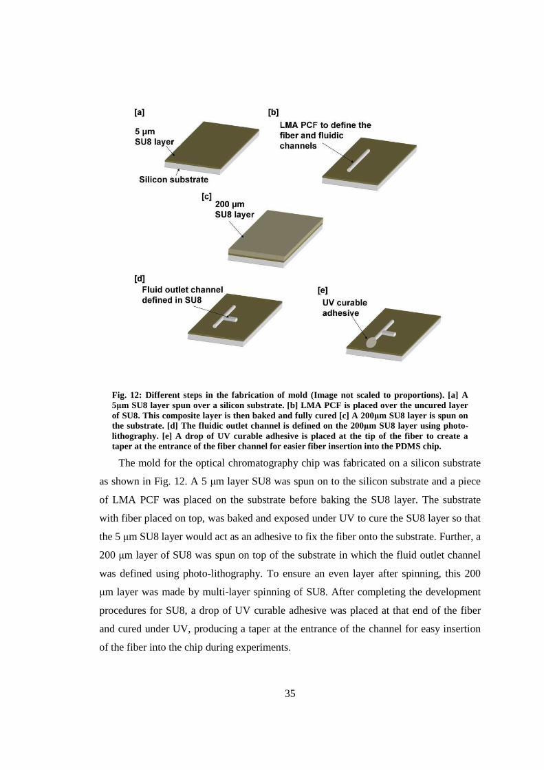
35
Fig. 12: Different steps in the fabrication of mold (Image not scaled to proportions). [a] A 5µm SU8 layer spun over a silicon substrate. [b] LMA PCF is placed over the uncured layer of SU8. This composite layer is then baked and fully cured [c] A 200µm SU8 layer is spun on the substrate. [d] The fluidic outlet channel is defined on the 200µm SU8 layer using photo-lithography. [e] A drop of UV curable adhesive is placed at the tip of the fiber to create a taper at the entrance of the fiber channel for easier fiber insertion into the PDMS chip.
The mold for the optical chromatography chip was fabricated on a silicon substrate
as shown in Fig. 12. A 5 µm layer SU8 was spun on to the silicon substrate and a piece
of LMA PCF was placed on the substrate before baking the SU8 layer. The substrate
with fiber placed on top, was baked and exposed under UV to cure the SU8 layer so that
the 5 µm SU8 layer would act as an adhesive to fix the fiber onto the substrate. Further, a
200 µm layer of SU8 was spun on top of the substrate in which the fluid outlet channel
was defined using photo-lithography. To ensure an even layer after spinning, this 200
µm layer was made by multi-layer spinning of SU8. After completing the development
procedures for SU8, a drop of UV curable adhesive was placed at that end of the fiber
and cured under UV, producing a taper at the entrance of the channel for easy insertion
of the fiber into the chip during experiments.
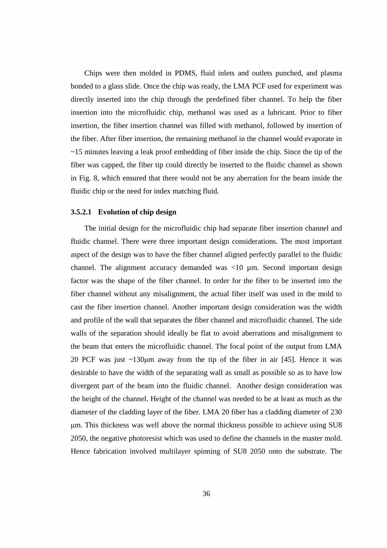
36
Chips were then molded in PDMS, fluid inlets and outlets punched, and plasma
bonded to a glass slide. Once the chip was ready, the LMA PCF used for experiment was
directly inserted into the chip through the predefined fiber channel. To help the fiber
insertion into the microfluidic chip, methanol was used as a lubricant. Prior to fiber
insertion, the fiber insertion channel was filled with methanol, followed by insertion of
the fiber. After fiber insertion, the remaining methanol in the channel would evaporate in
~15 minutes leaving a leak proof embedding of fiber inside the chip. Since the tip of the
fiber was capped, the fiber tip could directly be inserted to the fluidic channel as shown
in Fig. 8, which ensured that there would not be any aberration for the beam inside the
fluidic chip or the need for index matching fluid.
3.5.2.1 Evolution of chip design
The initial design for the microfluidic chip had separate fiber insertion channel and
fluidic channel. There were three important design considerations. The most important
aspect of the design was to have the fiber channel aligned perfectly parallel to the fluidic
channel. The alignment accuracy demanded was <10 µm. Second important design
factor was the shape of the fiber channel. In order for the fiber to be inserted into the
fiber channel without any misalignment, the actual fiber itself was used in the mold to
cast the fiber insertion channel. Another important design consideration was the width
and profile of the wall that separates the fiber channel and microfluidic channel. The side
walls of the separation should ideally be flat to avoid aberrations and misalignment to
the beam that enters the microfluidic channel. The focal point of the output from LMA
20 PCF was just ~130µm away from the tip of the fiber in air [45]. Hence it was
desirable to have the width of the separating wall as small as possible so as to have low
divergent part of the beam into the fluidic channel. Another design consideration was
the height of the channel. Height of the channel was needed to be at least as much as the
diameter of the cladding layer of the fiber. LMA 20 fiber has a cladding diameter of 230
µm. This thickness was well above the normal thickness possible to achieve using SU8
2050, the negative photoresist which was used to define the channels in the master mold.
Hence fabrication involved multilayer spinning of SU8 2050 onto the substrate. The
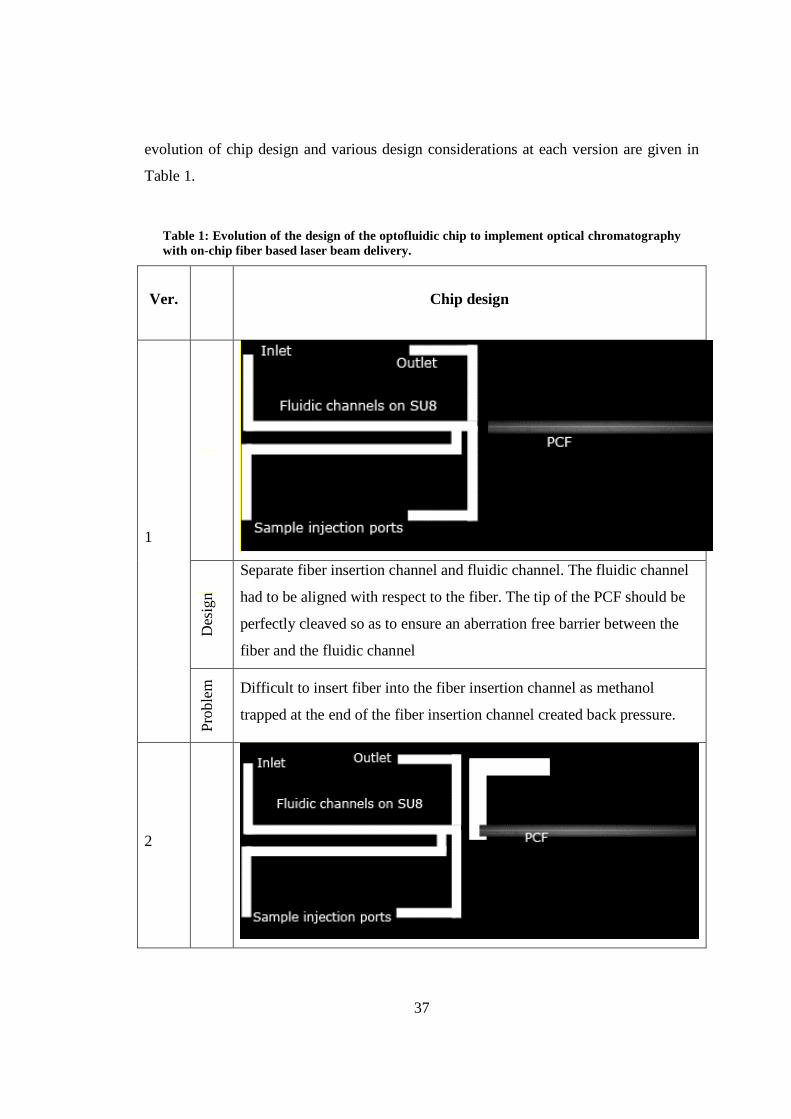
37
evolution of chip design and various design considerations at each version are given in
Table 1.
Table 1: Evolution of the design of the optofluidic chip to implement optical chromatography with on-chip fiber based laser beam delivery.
Ver. Chip design
1
D
esig
n
Separate fiber insertion channel and fluidic channel. The fluidic channel
had to be aligned with respect to the fiber. The tip of the PCF should be
perfectly cleaved so as to ensure an aberration free barrier between the
fiber and the fluidic channel
Pro
ble
m
Difficult to insert fiber into the fiber insertion channel as methanol
trapped at the end of the fiber insertion channel created back pressure.
2
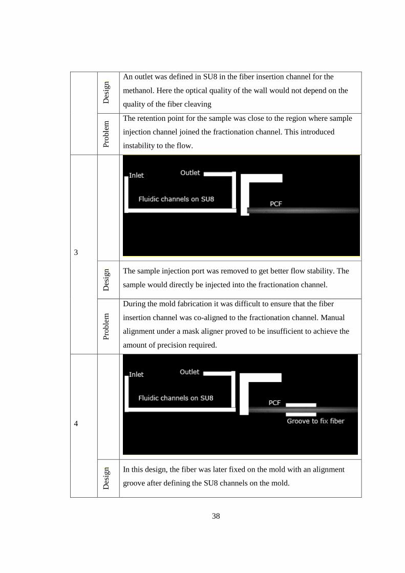
38
Des
ign An outlet was defined in SU8 in the fiber insertion channel for the
methanol. Here the optical quality of the wall would not depend on the
quality of the fiber cleaving P
robl
em The retention point for the sample was close to the region where sample
injection channel joined the fractionation channel. This introduced
instability to the flow.
3
Des
ign
The sample injection port was removed to get better flow stability. The
sample would directly be injected into the fractionation channel.
Pro
ble
m During the mold fabrication it was difficult to ensure that the fiber
insertion channel was co-aligned to the fractionation channel. Manual
alignment under a mask aligner proved to be insufficient to achieve the
amount of precision required.
4
Des
ign
In this design, the fiber was later fixed on the mold with an alignment
groove after defining the SU8 channels on the mold.
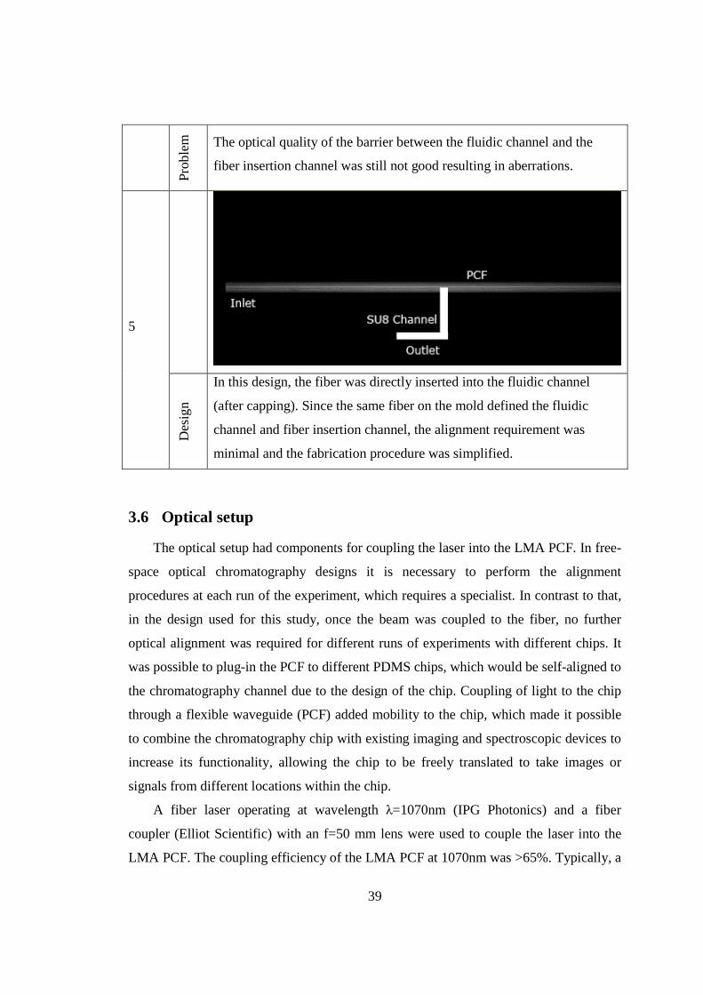
39
Pro
ble
m
The optical quality of the barrier between the fluidic channel and the
fiber insertion channel was still not good resulting in aberrations.
5
Des
ign
In this design, the fiber was directly inserted into the fluidic channel
(after capping). Since the same fiber on the mold defined the fluidic
channel and fiber insertion channel, the alignment requirement was
minimal and the fabrication procedure was simplified.
3.6 Optical setup
The optical setup had components for coupling the laser into the LMA PCF. In free-
space optical chromatography designs it is necessary to perform the alignment
procedures at each run of the experiment, which requires a specialist. In contrast to that,
in the design used for this study, once the beam was coupled to the fiber, no further
optical alignment was required for different runs of experiments with different chips. It
was possible to plug-in the PCF to different PDMS chips, which would be self-aligned to
the chromatography channel due to the design of the chip. Coupling of light to the chip
through a flexible waveguide (PCF) added mobility to the chip, which made it possible
to combine the chromatography chip with existing imaging and spectroscopic devices to
increase its functionality, allowing the chip to be freely translated to take images or
signals from different locations within the chip.
A fiber laser operating at wavelength λ=1070nm (IPG Photonics) and a fiber
coupler (Elliot Scientific) with an f=50 mm lens were used to couple the laser into the
LMA PCF. The coupling efficiency of the LMA PCF at 1070nm was >65%. Typically, a
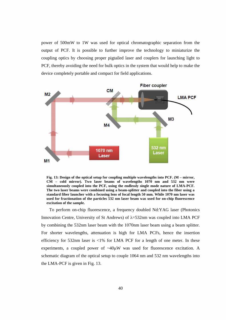
40
power of 500mW to 1W was used for optical chromatographic separation from the
output of PCF. It is possible to further improve the technology to miniaturize the
coupling optics by choosing proper pigtailed laser and couplers for launching light to
PCF, thereby avoiding the need for bulk optics in the system that would help to make the
device completely portable and compact for field applications.
Fig. 13: Design of the optical setup for coupling multiple wavelengths into PCF. (M – mirror, CM – cold mirror). Two laser beams of wavelengths 1070 nm and 532 nm were simultaneously coupled into the PCF, using the endlessly single mode nature of LMA-PCF. The two laser beams were combined using a beam-splitter and coupled into the fiber using a standard fiber launcher with a focusing lens of focal length 50 mm. While 1070 nm laser was used for fractionation of the particles 532 nm laser beam was used for on-chip fluorescence excitation of the sample.
To perform on-chip fluorescence, a frequency doubled Nd:YAG laser (Photonics
Innovation Centre, University of St Andrews) of λ=532nm was coupled into LMA PCF
by combining the 532nm laser beam with the 1070nm laser beam using a beam splitter.
For shorter wavelengths, attenuation is high for LMA PCFs, hence the insertion
efficiency for 532nm laser is <1% for LMA PCF for a length of one meter. In these
experiments, a coupled power of ~40µW was used for fluorescence excitation. A
schematic diagram of the optical setup to couple 1064 nm and 532 nm wavelengths into
the LMA-PCF is given in Fig. 13.
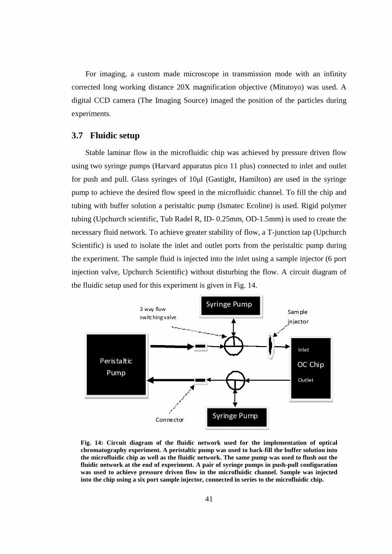
41
For imaging, a custom made microscope in transmission mode with an infinity
corrected long working distance 20X magnification objective (Mitutoyo) was used. A
digital CCD camera (The Imaging Source) imaged the position of the particles during
experiments.
3.7 Fluidic setup
Stable laminar flow in the microfluidic chip was achieved by pressure driven flow
using two syringe pumps (Harvard apparatus pico 11 plus) connected to inlet and outlet
for push and pull. Glass syringes of 10µl (Gastight, Hamilton) are used in the syringe
pump to achieve the desired flow speed in the microfluidic channel. To fill the chip and
tubing with buffer solution a peristaltic pump (Ismatec Ecoline) is used. Rigid polymer
tubing (Upchurch scientific, Tub Radel R, ID- 0.25mm, OD-1.5mm) is used to create the
necessary fluid network. To achieve greater stability of flow, a T-junction tap (Upchurch
Scientific) is used to isolate the inlet and outlet ports from the peristaltic pump during
the experiment. The sample fluid is injected into the inlet using a sample injector (6 port
injection valve, Upchurch Scientific) without disturbing the flow. A circuit diagram of
the fluidic setup used for this experiment is given in Fig. 14.
Fig. 14: Circuit diagram of the fluidic network used for the implementation of optical chromatography experiment. A peristaltic pump was used to back-fill the buffer solution into the microfluidic chip as well as the fluidic network. The same pump was used to flush out the fluidic network at the end of experiment. A pair of syringe pumps in push-pull configuration was used to achieve pressure driven flow in the microfluidic channel. Sample was injected into the chip using a six port sample injector, connected in series to the microfluidic chip.
42
3.8 Calibration of the system
The chromatography system was calibrated using dielectric spheres of silica and
polymer (Duke Scientific, Polysciences) of diameter 2µm, 3µm and 4µm. A ray optics
model was used to calculate the effective retention distance for particles of different
refractive indices and sizes for a given optical power and flow rate [24]. The ray optics
model for calculating the retention distance had been validated previously by comparing
it with a more rigorous model where optical radiation force was calculated by means of
Maxwell stress tensor, implemented using a finite element method [47]. Hence the ray
optics model was adopted here to calculate the retention distance for comparison with
the experimental values.
For the calibration, a 1070 nm fiber laser was coupled to the PCF and each type of
particle was separately injected into the chromatography device and the retention
distance recorded as a function of laser power and average flow speed. In all of the
experiments mentioned below, approximately 200 particles were injected to the
chromatography channel for one measurement. Fig. 15 shows the optical power verses
the retention distance for polystyrene and silica microspheres, and Fig. 16 shows the
average flow speed verses the retention distance graph. All the measurements of
retention distance were performed with ~10 particles held at the retention distance to
eliminate concentration-dependent effects.
At the retention region, the collected particles tend to move due to the dynamic
interaction of the particles with one another. For a higher number of particles held at the
retention distance (>30), the dynamic interaction creates instability for the concentrated
species and the retention distance of the species fluctuates beyond the resolution
required for spatial separation of different species (>400µm) as mentioned later in this
section. The maximum spread of a single species with the above specified concentration,
3 minutes after injecting the sample into the chip, was measured to be ~100µm,
compared to channel length of 1500µm over which spatial separation was performed.
Therefore an error bar of 100µm was assigned to the data shown in Fig. 15 and Fig. 16.
Following parameters were used to calculate the retention distance theoretically
using the ray optics model (equation 3.6). The beam parameters were obtained by beam-
profiling the output from the PCF.
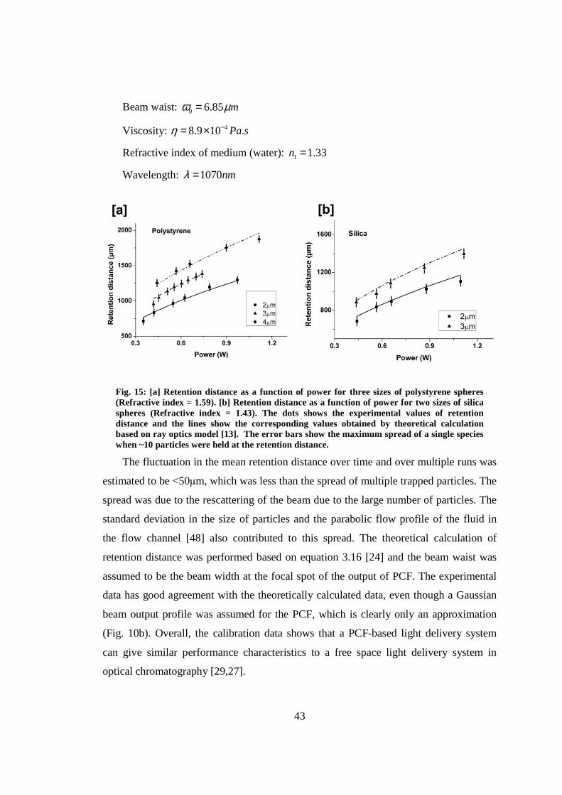
43
Beam waist: 0 6.85 mω µ=
Viscosity: 48.9 10 .Pa sη −= ×
Refractive index of medium (water): 1 1.33n =
Wavelength: 1070nmλ =
Fig. 15: [a] Retention distance as a function of power for three sizes of polystyrene spheres (Refractive index = 1.59). [b] Retention distance as a function of power for two sizes of silica spheres (Refractive index = 1.43). The dots shows the experimental values of retention distance and the lines show the corresponding values obtained by theoretical calculation based on ray optics model [13]. The error bars show the maximum spread of a single species when ~10 particles were held at the retention distance.
The fluctuation in the mean retention distance over time and over multiple runs was
estimated to be <50µm, which was less than the spread of multiple trapped particles. The
spread was due to the rescattering of the beam due to the large number of particles. The
standard deviation in the size of particles and the parabolic flow profile of the fluid in
the flow channel [48] also contributed to this spread. The theoretical calculation of
retention distance was performed based on equation 3.16 [24] and the beam waist was
assumed to be the beam width at the focal spot of the output of PCF. The experimental
data has good agreement with the theoretically calculated data, even though a Gaussian
beam output profile was assumed for the PCF, which is clearly only an approximation
(Fig. 10b). Overall, the calibration data shows that a PCF-based light delivery system
can give similar performance characteristics to a free space light delivery system in
optical chromatography [29,27].
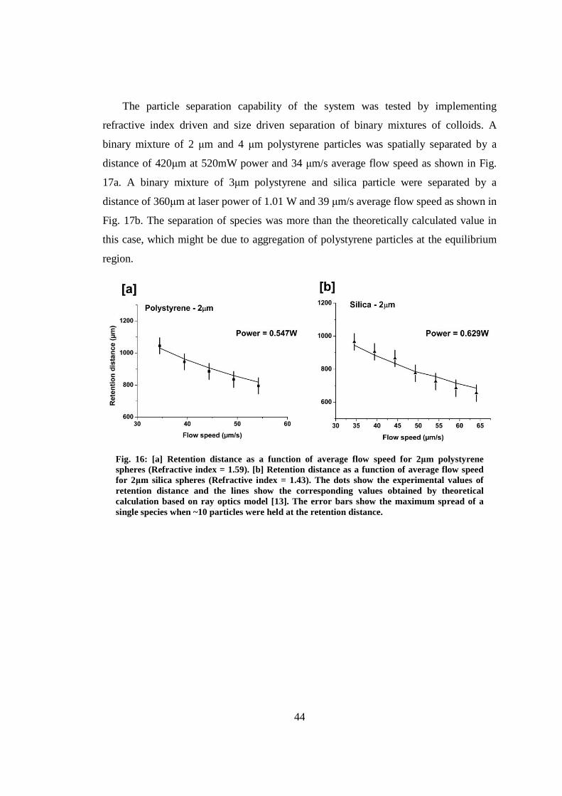
44
The particle separation capability of the system was tested by implementing
refractive index driven and size driven separation of binary mixtures of colloids. A
binary mixture of 2 µm and 4 µm polystyrene particles was spatially separated by a
distance of 420µm at 520mW power and 34 µm/s average flow speed as shown in Fig.
17a. A binary mixture of 3µm polystyrene and silica particle were separated by a
distance of 360µm at laser power of 1.01 W and 39 µm/s average flow speed as shown in
Fig. 17b. The separation of species was more than the theoretically calculated value in
this case, which might be due to aggregation of polystyrene particles at the equilibrium
region.
Fig. 16: [a] Retention distance as a function of average flow speed for 2µm polystyrene spheres (Refractive index = 1.59). [b] Retention distance as a function of average flow speed for 2µm silica spheres (Refractive index = 1.43). The dots show the experimental values of retention distance and the lines show the corresponding values obtained by theoretical calculation based on ray optics model [13]. The error bars show the maximum spread of a single species when ~10 particles were held at the retention distance.
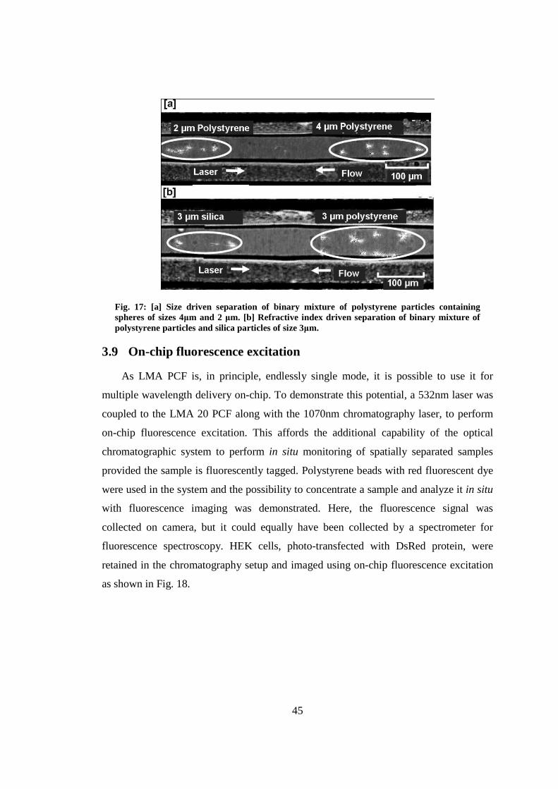
45
Fig. 17: [a] Size driven separation of binary mixture of polystyrene particles containing spheres of sizes 4µm and 2 µm. [b] Refractive index driven separation of binary mixture of polystyrene particles and silica particles of size 3µm.
3.9 On-chip fluorescence excitation
As LMA PCF is, in principle, endlessly single mode, it is possible to use it for
multiple wavelength delivery on-chip. To demonstrate this potential, a 532nm laser was
coupled to the LMA 20 PCF along with the 1070nm chromatography laser, to perform
on-chip fluorescence excitation. This affords the additional capability of the optical
chromatographic system to perform in situ monitoring of spatially separated samples
provided the sample is fluorescently tagged. Polystyrene beads with red fluorescent dye
were used in the system and the possibility to concentrate a sample and analyze it in situ
with fluorescence imaging was demonstrated. Here, the fluorescence signal was
collected on camera, but it could equally have been collected by a spectrometer for
fluorescence spectroscopy. HEK cells, photo-transfected with DsRed protein, were
retained in the chromatography setup and imaged using on-chip fluorescence excitation
as shown in Fig. 18.
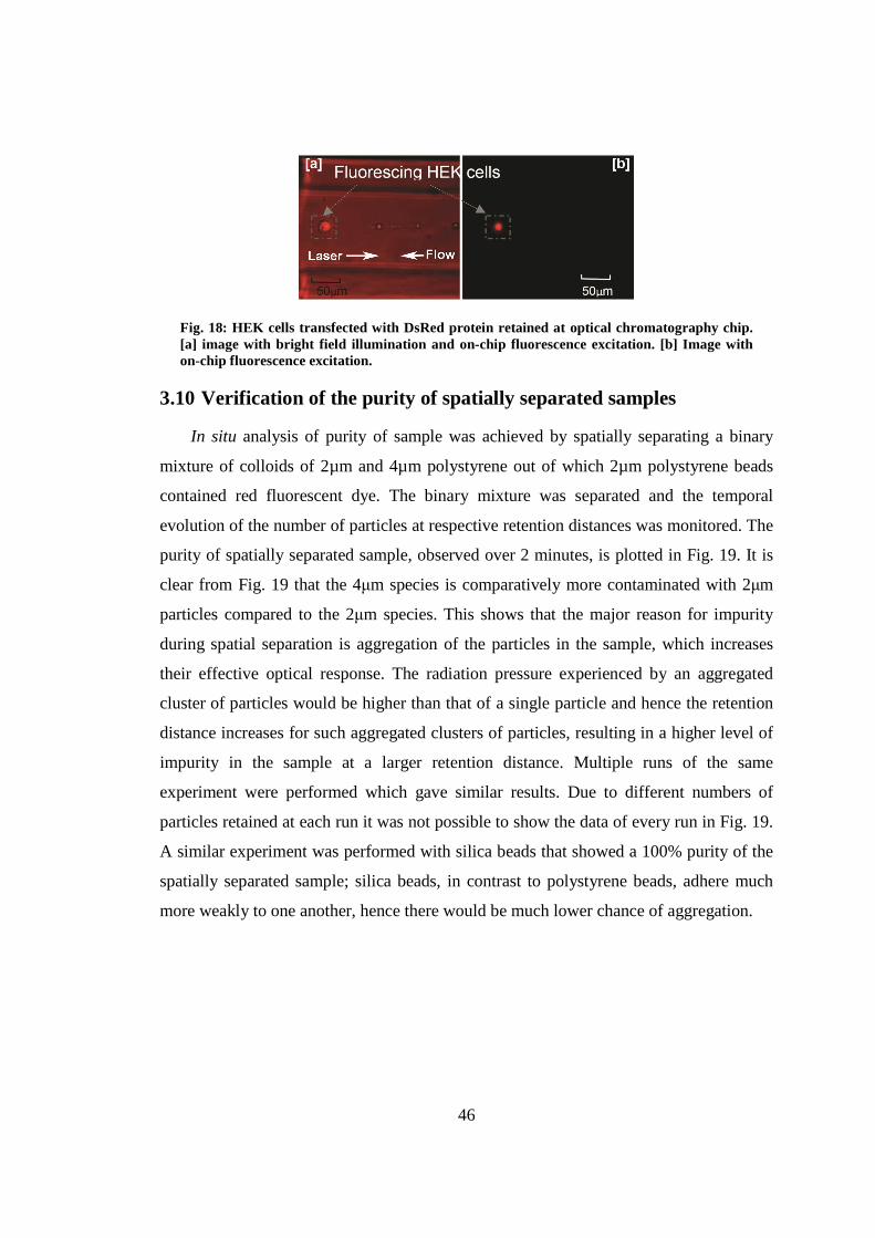
46
Fig. 18: HEK cells transfected with DsRed protein retained at optical chromatography chip. [a] image with bright field illumination and on-chi p fluorescence excitation. [b] Image with on-chip fluorescence excitation.
3.10 Verification of the purity of spatially separated samples
In situ analysis of purity of sample was achieved by spatially separating a binary
mixture of colloids of 2µm and 4µm polystyrene out of which 2µm polystyrene beads
contained red fluorescent dye. The binary mixture was separated and the temporal
evolution of the number of particles at respective retention distances was monitored. The
purity of spatially separated sample, observed over 2 minutes, is plotted in Fig. 19. It is
clear from Fig. 19 that the 4µm species is comparatively more contaminated with 2µm
particles compared to the 2µm species. This shows that the major reason for impurity
during spatial separation is aggregation of the particles in the sample, which increases
their effective optical response. The radiation pressure experienced by an aggregated
cluster of particles would be higher than that of a single particle and hence the retention
distance increases for such aggregated clusters of particles, resulting in a higher level of
impurity in the sample at a larger retention distance. Multiple runs of the same
experiment were performed which gave similar results. Due to different numbers of
particles retained at each run it was not possible to show the data of every run in Fig. 19.
A similar experiment was performed with silica beads that showed a 100% purity of the
spatially separated sample; silica beads, in contrast to polystyrene beads, adhere much
more weakly to one another, hence there would be much lower chance of aggregation.
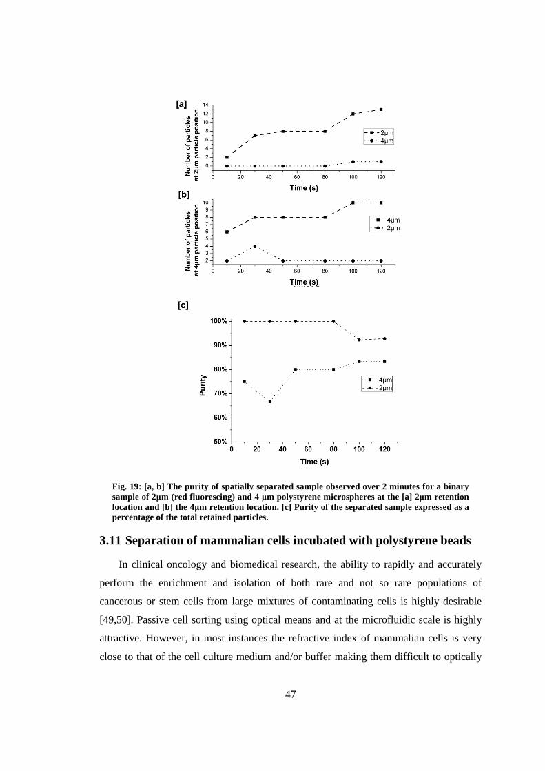
47
Fig. 19: [a, b] The purity of spatially separated sample observed over 2 minutes for a binary sample of 2µm (red fluorescing) and 4 µm polystyrene microspheres at the [a] 2µm retention location and [b] the 4µm retention location. [c] Purity of the separated sample expressed as a percentage of the total retained particles.
3.11 Separation of mammalian cells incubated with polystyrene beads
In clinical oncology and biomedical research, the ability to rapidly and accurately
perform the enrichment and isolation of both rare and not so rare populations of
cancerous or stem cells from large mixtures of contaminating cells is highly desirable
[49,50]. Passive cell sorting using optical means and at the microfluidic scale is highly
attractive. However, in most instances the refractive index of mammalian cells is very
close to that of the cell culture medium and/or buffer making them difficult to optically
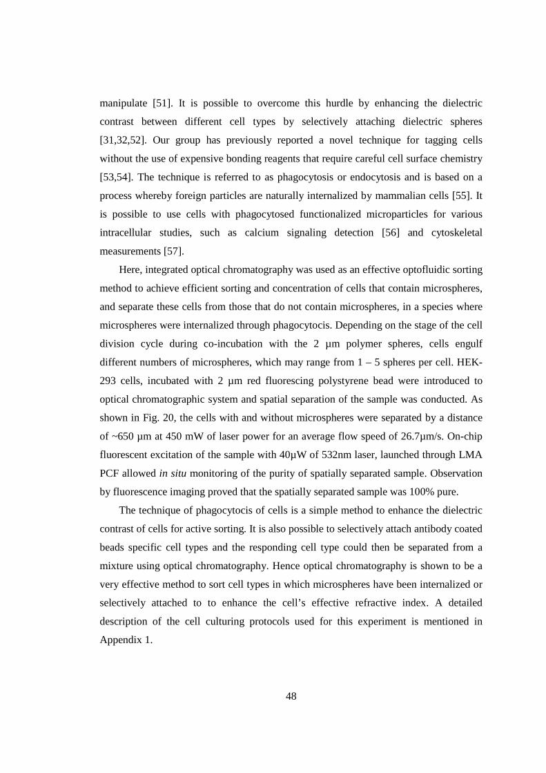
48
manipulate [51]. It is possible to overcome this hurdle by enhancing the dielectric
contrast between different cell types by selectively attaching dielectric spheres
[31,32,52]. Our group has previously reported a novel technique for tagging cells
without the use of expensive bonding reagents that require careful cell surface chemistry
[53,54]. The technique is referred to as phagocytosis or endocytosis and is based on a
process whereby foreign particles are naturally internalized by mammalian cells [55]. It
is possible to use cells with phagocytosed functionalized microparticles for various
intracellular studies, such as calcium signaling detection [56] and cytoskeletal
measurements [57].
Here, integrated optical chromatography was used as an effective optofluidic sorting
method to achieve efficient sorting and concentration of cells that contain microspheres,
and separate these cells from those that do not contain microspheres, in a species where
microspheres were internalized through phagocytocis. Depending on the stage of the cell
division cycle during co-incubation with the 2 µm polymer spheres, cells engulf
different numbers of microspheres, which may range from 1 – 5 spheres per cell. HEK-
293 cells, incubated with 2 µm red fluorescing polystyrene bead were introduced to
optical chromatographic system and spatial separation of the sample was conducted. As
shown in Fig. 20, the cells with and without microspheres were separated by a distance
of ~650 µm at 450 mW of laser power for an average flow speed of 26.7µm/s. On-chip
fluorescent excitation of the sample with 40µW of 532nm laser, launched through LMA
PCF allowed in situ monitoring of the purity of spatially separated sample. Observation
by fluorescence imaging proved that the spatially separated sample was 100% pure.
The technique of phagocytocis of cells is a simple method to enhance the dielectric
contrast of cells for active sorting. It is also possible to selectively attach antibody coated
beads specific cell types and the responding cell type could then be separated from a
mixture using optical chromatography. Hence optical chromatography is shown to be a
very effective method to sort cell types in which microspheres have been internalized or
selectively attached to to enhance the cell’s effective refractive index. A detailed
description of the cell culturing protocols used for this experiment is mentioned in
Appendix 1.
49
Fig. 20: Separation of HEK cells incubated with red fluorescing polystyrene microspheres. [a] with bright field illumination and fluorescent illu mination [b] without bright field illumination and with fluorescent excitation.
3.12 Conclusion
The techniques for sorting or fractionating cells have played a crucial role in the
advancement of biotechnology over past three decades. Although active sorting
techniques like fluorescence activated cell sorting (FACS) have made it possible to
achieve high throughput cell fractionation, the necessity to attach external dyes makes it
a sample specific technique [58]. There are some types of cells which cannot be sorted
using conventional active sorting techniques. Hence, although there are well established
and widely used active techniques are available for cell fractionation; there is still room
for developing novel techniques for cell fractionation. The advancement in the field of
microfluidics over the past two decades opens up new opportunities to implement cell
fractionation techniques in a variety of new geometries. Optical detection technique has
played a crucial role in the development of FACS. While light was used as a probe in
such active sorting techniques, it is possible to utilize the radiation force of light to
achieve passive fractionation of cells based on the inherent properties of the sample
such as size, shape or refractive index [31].
Optical chromatography is one such passive cell fractionation technique, which was
used for several applications over last 10 years. This technique utilizes the interplay
between the viscous drag force and optical radiation force to achieve fractionation of
50
cells [24]. Although this technique has been used for several practical applications in a
variety of microfluidic geometry the means for beam delivery into the chip remained as
free-space coupling. This poses a serious limitation for this technique as this result in
bigger form factor of the whole system and also it required highly precise optical
alignment for each run. In this study, this issue was tackled by implementing fiber based
optical beam delivery into the chip.
A novel optical chromatography chip, with integrated launching optics using PCF
was successfully implemented and the capability of the system to separate different
species of colloidal particles was demonstrated. The soft-lithography protocol was
modified for microfluidic chip fabrication so as to achieve pre-defined fiber insertion
channel to which PCF could be embedded in a leak-proof manner. A special capping
method was also devised for sealing the holes at the cleaved face of PCF, without
distorting the output beam profile of PCF. This capping method allowed us to insert the
PCF directly into the microfluidic channel as the cap prevented the suction of buffer
solution into the holes of PCF through capillary action. Since the optical fiber could be
embedded into the microfluidic chip without any PDMS wall between the fluidic
channel and the end face of fiber, optical beam could be delivered into the fluidic
channel without any aberration.
This optofluidic device was validated by estimating the retention distance of
colloidal particles of different size and different refractive index. Since the resultant
retention distance was in good agreement with theory, it could be concluded that the
resolution of the system was on par with the conventional optical chromatography
approaches in which free-space optics were used to couple light into the microfluidic
channel. Further, refractive index driven and size driven separation of colloids were alos
demonstrated using this optofluidic device. The endlessly single mode nature of LMA
PCF allowed us to launch multiple wavelengths through the fiber to achieve multi-
modality by combining optical chromatography with on-chip fluorescence excitation,
allowing in situ monitoring of the sample during spatial separation. The retention and
concentration of HEK cells was achieved to demonstrate the capability of the system to
sort biological particles. Integrated optical chromatography is shown to be an effective
optofluidic sorting method to achieve active sorting of cells internalized with
51
microspheres through phagocytocis, highlighting the flexibility of optical
chromatography to be used as both an active and passive sorting technique.
The approach based on embedded PCF makes optical chromatography an effective
tool to be used with PDMS or indeed other common microfluidic chip materials, and
removes the need for free space optical alignment. Also this opens up opportunity to
develop devices based on optical chromatography for field applications.
Relevant Publications
• Ashok PC, Marchington RF, Mthunzi P, Krauss TF, Dholakia K (2010)
Optical chromatography using a photonic crystal fiber with on-chip
fluorescence excitation. Opt Express 18 (6):6396-6407
• Ashok PC, Marchington RF, Mazilu M, Krauss TF, Dholakia K Towards
integrated optical chromatography using photonic crystal fiber. In: Dholakia
K, Spalding GC (eds), 2009. SPIE, p 74000R
Patent
• Application: The University of St. Andrews, Marchington RF, Ashok P.,
Dholakia K., “Optical Trap”, WO/2010/007371 A2
Contributions
P. C. Ashok designed and fabricated the microfluidic chip, setup the optical and
fluidics systems for the optical chromatography experiment. R. F. Marchington assisted
P. C. Ashok in implementing the experimental setup. P. Mthunzi prepared the cell
samples required for this experiment.
52
4. Towards passive optical cell sorting in an optofluidic chip using optical landscapes
4.1 Introduction
As discussed in chapter 3, cell sorting techniques are important tools in the field of
biotechnology. Cell sorting techniques can be broadly classified into active and passive
sorting techniques. Passive sorting technique relies on the differences in the inherent
physical properties of the sample. The sample respond differently based on a specific
physical parameter (eg. Size, shape, rigidity, refractive index and mobility), which
allows fractionation. There have been several non-optical techniques demonstrated for
passive sorting of cells which includes centrifugal sorting [59,60], field flow
fractionation [61,62], hydrophoretic fractionation [63,64], magnetic activated cell sorting
[65,66] and dielectrophoretic fractionation [67-69].
Although optical sorting techniques play a prominent role in cell sorting strategies,
they are mainly limited to active sorting techniques. Active optical sorting involves a
two stage process. First the sample passes through an optical detection region, where the
characteristics of the sample would be probed using optical techniques such as scattering
and spectroscopy. The second stage is the deflection region where, based on the
characteristics of the sample assessed from the information obtained from the detection
region, the sample would be deflected into its designated channel. Fluorescence
activated cell sorting (FACS) is a widely used technique which allows high throughput
fractionation of cells (~ 40000 cells/s) [70]. In FACS cells may be tagged with external
probes such as dyes or fluorescent proteins as an indicative of the cell functionality
[71,72]. Another burgeoning active optical sorting technique is Raman activated cell
sorting (RACS), where instead of fluorescence spectroscopy, Raman spectroscopy is
used to achieve cell fractionation. Although the throughput of RACS is well below
FACS, the prospectus of sorting cells without the need of any external tag makes RACS
a promising technique [73,74].
Another competing approach is passive optical cell sorting, where fractionation
relies on the differences in optical forces experienced by different types of cells due to
the difference in size, shape or refractive index. One such passive fractionation
technique, optical chromatography, is already detailed in chapter 3. Another technique
53
for passive optical fractionation is by using optical landscape created by multiple optical
traps [31]. Several approaches were demonstrated for passive sorting of dielectric
particles of varying size or shape using such optical landscapes, including Bessel beam
sorting [52], optical lattice sorting [75], acousto-optically generated potential energy
landscape based sorting [76], holographic optical tweezers based optical landscape
sorting [77] and evanescent wave sorting [78].
Although passive optical fractionation of microparticles was theoretically proposed
[79] and experimentally demonstrated [77,76], such works were mainly limited to
fractionation of dielectric particles. No technology is yet developed to achieve high
throughput passive sorting of cells in a microfluidic environment. With the progress in
the field of passive optical sorting technology over recent years, the technology is now
matured enough to be pushed towards device level applications. In order to achieve a
passive optical cell sorting device, an optical tweezers system for the generation of
optical landscape should be combined with a microfluidic chip, through which cells are
to be flown and fractionated. Unlike fractionation of dielectric particles with definite
size, shape and refractive index, the variance in the physical properties within a single
species of cells makes passive sorting of cells challenging. The fact that the physical
properties like size shape or refractive index are unknown makes the design of the
microfluidic chip and optical landscape even more challenging.
This chapter describes initial attempts towards developing a passive optical cell
sorting system by combining a microfluidic platform with an optical tweezers system
equipped with a Dual Axis - Acousto Optic Deflector (DA-AOD) for creating optical
landscapes with time-shared multiple optical traps.
4.2 Optical trapping system with a DA- AOD – optical design and interface
Multiple trapping can only be realized in an optical trapping system by time
multiplexing [80,81] or space multiplexing [82,83] of single traps. Time multiplexed
optical traps, realized by acousto-optic technology is one of the popular ways to produce
optical landscapes [76]. In this work, such a DA-AOD based optical trapping setup was
used for creating optical landscape inside a microfluidic chip.
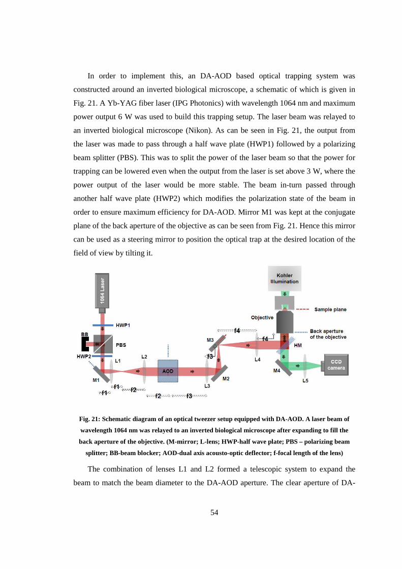
54
In order to implement this, an DA-AOD based optical trapping system was
constructed around an inverted biological microscope, a schematic of which is given in
Fig. 21. A Yb-YAG fiber laser (IPG Photonics) with wavelength 1064 nm and maximum
power output 6 W was used to build this trapping setup. The laser beam was relayed to
an inverted biological microscope (Nikon). As can be seen in Fig. 21, the output from
the laser was made to pass through a half wave plate (HWP1) followed by a polarizing
beam splitter (PBS). This was to split the power of the laser beam so that the power for
trapping can be lowered even when the output from the laser is set above 3 W, where the
power output of the laser would be more stable. The beam in-turn passed through
another half wave plate (HWP2) which modifies the polarization state of the beam in
order to ensure maximum efficiency for DA-AOD. Mirror M1 was kept at the conjugate
plane of the back aperture of the objective as can be seen from Fig. 21. Hence this mirror
can be used as a steering mirror to position the optical trap at the desired location of the
field of view by tilting it.
Fig. 21: Schematic diagram of an optical tweezer setup equipped with DA-AOD. A laser beam of
wavelength 1064 nm was relayed to an inverted biological microscope after expanding to fill the
back aperture of the objective. (M-mirror; L-lens; HWP-half wave plate; PBS – polarizing beam
splitter; BB-beam blocker; AOD-dual axis acousto-optic deflector; f-focal length of the lens)
The combination of lenses L1 and L2 formed a telescopic system to expand the
beam to match the beam diameter to the DA-AOD aperture. The clear aperture of DA-
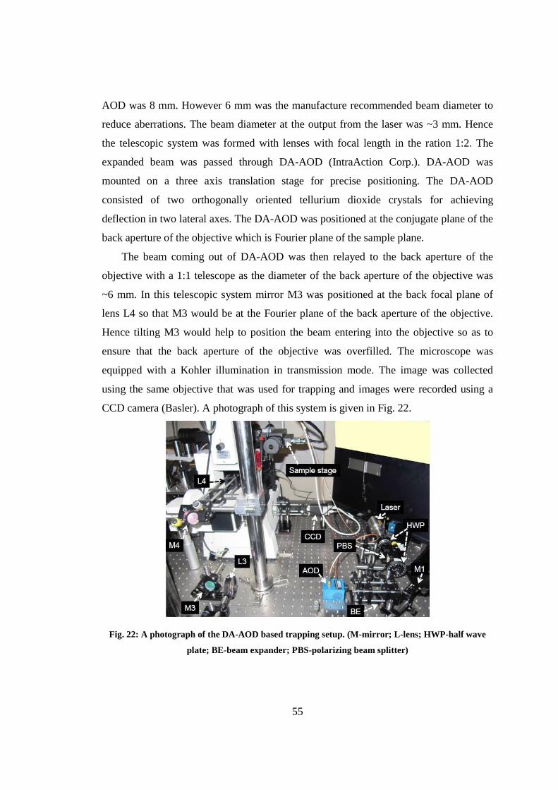
55
AOD was 8 mm. However 6 mm was the manufacture recommended beam diameter to
reduce aberrations. The beam diameter at the output from the laser was ~3 mm. Hence
the telescopic system was formed with lenses with focal length in the ration 1:2. The
expanded beam was passed through DA-AOD (IntraAction Corp.). DA-AOD was
mounted on a three axis translation stage for precise positioning. The DA-AOD
consisted of two orthogonally oriented tellurium dioxide crystals for achieving
deflection in two lateral axes. The DA-AOD was positioned at the conjugate plane of the
back aperture of the objective which is Fourier plane of the sample plane.
The beam coming out of DA-AOD was then relayed to the back aperture of the
objective with a 1:1 telescope as the diameter of the back aperture of the objective was
~6 mm. In this telescopic system mirror M3 was positioned at the back focal plane of
lens L4 so that M3 would be at the Fourier plane of the back aperture of the objective.
Hence tilting M3 would help to position the beam entering into the objective so as to
ensure that the back aperture of the objective was overfilled. The microscope was
equipped with a Kohler illumination in transmission mode. The image was collected
using the same objective that was used for trapping and images were recorded using a
CCD camera (Basler). A photograph of this system is given in Fig. 22.
Fig. 22: A photograph of the DA-AOD based trapping setup. (M-mirror; L-lens; HWP-half wave
plate; BE-beam expander; PBS-polarizing beam splitter)
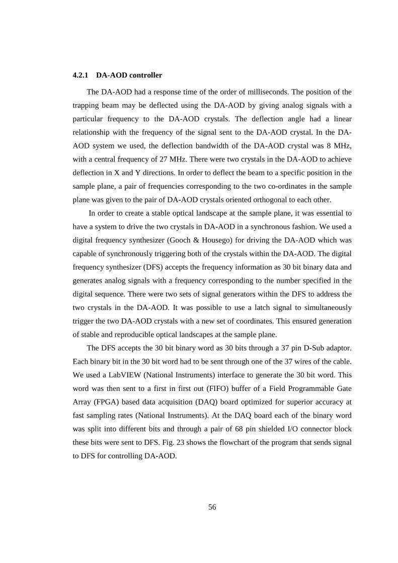
56
4.2.1 DA-AOD controller
The DA-AOD had a response time of the order of milliseconds. The position of the
trapping beam may be deflected using the DA-AOD by giving analog signals with a
particular frequency to the DA-AOD crystals. The deflection angle had a linear
relationship with the frequency of the signal sent to the DA-AOD crystal. In the DA-
AOD system we used, the deflection bandwidth of the DA-AOD crystal was 8 MHz,
with a central frequency of 27 MHz. There were two crystals in the DA-AOD to achieve
deflection in X and Y directions. In order to deflect the beam to a specific position in the
sample plane, a pair of frequencies corresponding to the two co-ordinates in the sample
plane was given to the pair of DA-AOD crystals oriented orthogonal to each other.
In order to create a stable optical landscape at the sample plane, it was essential to
have a system to drive the two crystals in DA-AOD in a synchronous fashion. We used a
digital frequency synthesizer (Gooch & Housego) for driving the DA-AOD which was
capable of synchronously triggering both of the crystals within the DA-AOD. The digital
frequency synthesizer (DFS) accepts the frequency information as 30 bit binary data and
generates analog signals with a frequency corresponding to the number specified in the
digital sequence. There were two sets of signal generators within the DFS to address the
two crystals in the DA-AOD. It was possible to use a latch signal to simultaneously
trigger the two DA-AOD crystals with a new set of coordinates. This ensured generation
of stable and reproducible optical landscapes at the sample plane.
The DFS accepts the 30 bit binary word as 30 bits through a 37 pin D-Sub adaptor.
Each binary bit in the 30 bit word had to be sent through one of the 37 wires of the cable.
We used a LabVIEW (National Instruments) interface to generate the 30 bit word. This
word was then sent to a first in first out (FIFO) buffer of a Field Programmable Gate
Array (FPGA) based data acquisition (DAQ) board optimized for superior accuracy at
fast sampling rates (National Instruments). At the DAQ board each of the binary word
was split into different bits and through a pair of 68 pin shielded I/O connector block
these bits were sent to DFS. Fig. 23 shows the flowchart of the program that sends signal
to DFS for controlling DA-AOD.
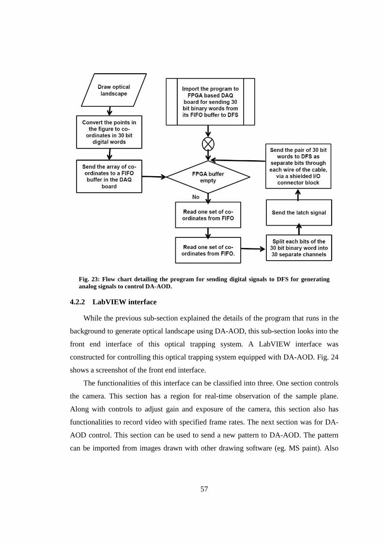
57
Fig. 23: Flow chart detailing the program for sending digital signals to DFS for generating analog signals to control DA-AOD.
4.2.2 LabVIEW interface
While the previous sub-section explained the details of the program that runs in the
background to generate optical landscape using DA-AOD, this sub-section looks into the
front end interface of this optical trapping system. A LabVIEW interface was
constructed for controlling this optical trapping system equipped with DA-AOD. Fig. 24
shows a screenshot of the front end interface.
The functionalities of this interface can be classified into three. One section controls
the camera. This section has a region for real-time observation of the sample plane.
Along with controls to adjust gain and exposure of the camera, this section also has
functionalities to record video with specified frame rates. The next section was for DA-
AOD control. This section can be used to send a new pattern to DA-AOD. The pattern
can be imported from images drawn with other drawing software (eg. MS paint). Also
58
this interface has a third section which is a drawing board which can be used to draw
desired patterns to be sent to DA-AOD.
Fig. 24: Front end interface of to generate optical landscape using DA-AOD based optical trapping
system.
As can be seen in Fig. 24, the LabVIEW based interface is equipped with drawing
board and recording functions which make it suitable to create desired optical landscape
and to observe and record it in real-time.
4.3 Theory of optical landscape sorting using a line trap
When microscopic dielectric particles are driven through a periodic potential energy
landscape produced by optical traps, if the object satisfy certain criteria, it can get locked
into a symmetry-selected direction, which is independent of the direction of the driving
force [84]. The criteria to get locked-in depend on the size, shape or refractive index of
the object. This is the basis of passive optical sorting of microscopic particles. The
conditions for an object to get locked in vary depending on the geometry of optical
landscape. This section briefly discusses the formulation of criteria to use a simple line
optical trap for fractionation of microparticles in a microfluidic flow.
59
The potential of the Gaussian well of an optical trap can be expressed as [84]:
( )2
1 0 2exp
2 p
rV r V
σ
= −
(4.1)
Where, pσ is the effective width of linear array, which can be expressed as:
22 2
24pm
an
λσ = + (4.2)
a is the radius of micro-particle, λ is the wavelength of laser and mn is the
refractive index of the medium.
0V can be expressed as [77]:
2 23
0 2 2 22p mm
p p m
n nn aV P
c n nσ −
= + (4.3)
Where, pn is the refractive index of the particle, P is the power of the laser beam.
When an array of such Gaussian wells separated by a distance b is formed, the
effective potential energy can be expressed as [84]:
( )ɵ( )2
0 2exp
2n p
r nbxV r V
σ
− = −
∑
(4.4)
Where, ɵx is the unit vector in the direction of the line trap.
The objects that are locked into the periodic potential landscape would have
periodic trajectories with a series of turning points. There are two types of turning points
on such trajectories; one at the center of a trap and the other at the midway between two
traps. For moderate anglesθ for the orientation of the line trap with respect to the
direction of driving force, those trajectories which would not have or which will have the
weakest turning point between two traps would escape out of the trajectory of the line
trap. The condition for the maximum angle below which the object is trapped into the
periodic potential is given by [77,79,84]:
21 0
2
2sin exp
1 8exp2
MAXp p
V b
Fθ
σ σ−
≤ −
(4.5)
60
Where, F is the driving force. In this case this corresponds to the viscous drag
force.
6F avπη= (4.6)
Where, v is the flow velocity and η is the viscosity of the fluid.
Rearranging equation 4.5 gives a function which defines the boundary in the size vs.
refractive index plane for those objects that would be locked-in of a line trap with a
specific angle, distance between traps and power. This function is given by the equation
[77]:
( ) 2 ( )( )
( ) ( )c m
A a B an a n
A a B a
+=−
(4.7)
Where,
2 23
3exp
8 pp
a b bA σ
σ
= −
(4.8)
6sin
2 m
e vcB b
n P
πη θ= (4.9)
Where, θ is the angle of the line trap with respect to the direction of the driving
force.
Function ( )cn a draws the boundary in the size vs. refractive index plane, the
particles which lies above this line would get locked into the line trap whereas the
particles which are below would not be. From equations 4.7 – 4.9 it can be seen that for
a system with given wavelength (λ ) for the traps, viscosity of the buffer (η ), to
differentiate two species of samples with varying size or refractive index there are
mainly four tunable parameters that have to be optimized. These four parameters are
flow velocity (v ), angle of orientation of line trap with respect to the drive force (θ ),
distance between two traps in the line trap (b ) and power per trap (P ).
To achieve fractionation of two types of colloidal particles with known size and
refractive indices, it is essential to find the right set of these tunable parameters. In order
to do that, a numerical code based on the theory explained above was written in
Mathematica (Wolfram). In this code it was possible to visually choose the right set of
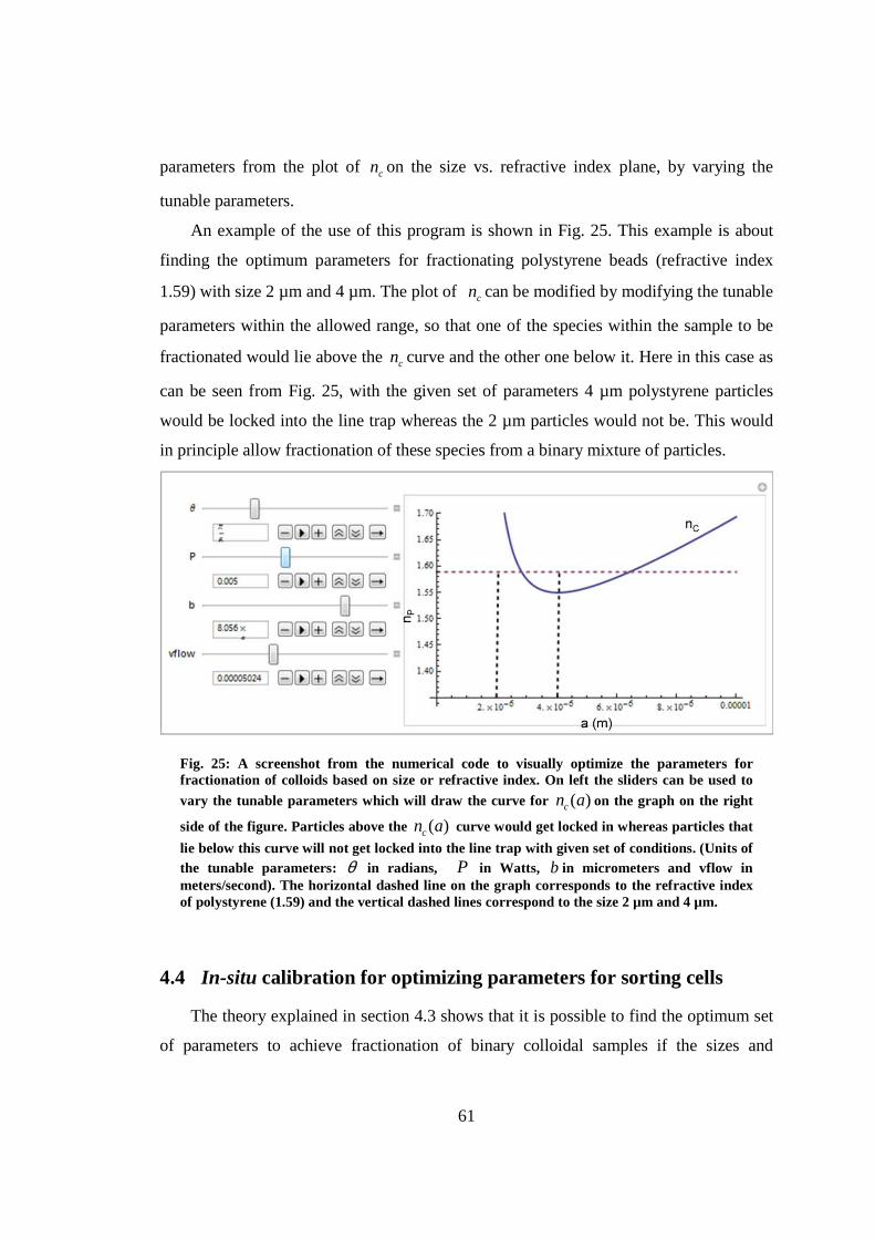
61
parameters from the plot of cn on the size vs. refractive index plane, by varying the
tunable parameters.
An example of the use of this program is shown in Fig. 25. This example is about
finding the optimum parameters for fractionating polystyrene beads (refractive index
1.59) with size 2 µm and 4 µm. The plot of cn can be modified by modifying the tunable
parameters within the allowed range, so that one of the species within the sample to be
fractionated would lie above the cn curve and the other one below it. Here in this case as
can be seen from Fig. 25, with the given set of parameters 4 µm polystyrene particles
would be locked into the line trap whereas the 2 µm particles would not be. This would
in principle allow fractionation of these species from a binary mixture of particles.
Fig. 25: A screenshot from the numerical code to visually optimize the parameters for fractionation of colloids based on size or refractive index. On left the sliders can be used to
vary the tunable parameters which will draw the curve for ( )cn a on the graph on the right
side of the figure. Particles above the ( )cn a curve would get locked in whereas particles that
lie below this curve will not get locked into the line trap with given set of conditions. (Units of the tunable parameters: θ in radians, P in Watts, b in micrometers and vflow in meters/second). The horizontal dashed line on the graph corresponds to the refractive index of polystyrene (1.59) and the vertical dashed lines correspond to the size 2 µm and 4 µm.
4.4 In-situ calibration for optimizing parameters for sorting cells
The theory explained in section 4.3 shows that it is possible to find the optimum set
of parameters to achieve fractionation of binary colloidal samples if the sizes and
62
refractive indices of the particles to be fractionated are known. In principle the same
theory can be extrapolated to achieve fractionation of cells. However the sizes and
refractive indices of the cells to be sorted are unknown, which makes it practically
difficult to optimize the system and to choose the right set of parameters to obtain
fractionation of cells using optical landscape. The non-spherical shape of cells makes the
task further complicated. Other unknown parameters are the viscosity and refractive
index of the buffer medium where cells have to be suspended. With all these unknown
parameters, the four parameter space of the tunable parameters makes it practically
impossible to find the optimum set by a trial and error approach.
A solution to this would be to draw an analogy between a spherical colloidal particle
with known size and refractive index and a particular species of cell. Fundamentally
fractionation of micro-particle in an optical landscape is facilitated by the interplay
between the optical radiation force and viscous drag force. If it is possible to find a
spherical colloidal particle (eg. polystyrene bead) which interacts with the optical trap,
while in a flow similar to that of a particular cell species which is to be fractionated, then
it is possible to optimize the parameters for line trap based cell sorter based on the size
and refractive index of the colloidal particle.
An in situ calibration may be performed to find the spherical colloidal particle
whose interaction is similar to that of a cell in the flow-optical trapping system. A drag
force method can be used to find a figure of merit which is directly related to the Q-
value of the trap. The Q-value is a dimensionless number which relates to the efficiency
of transfer of momentum from the optical beam to the particle which can be expressed as
[85]:
dm
cQ F
n P= (4.10)
Where, dF is the drag force which may be required to remove the particle from the
trap may be calculated from equation 4.6, for a given optical power P in a fluid of
refractive index mn . Equation 4.10 shows that Q value depends on the refractive index
and viscosity of the buffer medium which is unknown in this case. Hence it is not
possible to measure Q value in this case. However it is possible to estimate the fluid
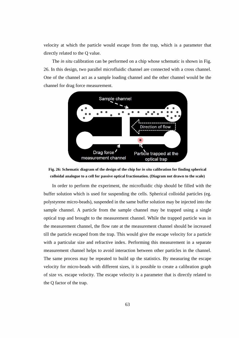
63
velocity at which the particle would escape from the trap, which is a parameter that
directly related to the Q value.
The in situ calibration can be performed on a chip whose schematic is shown in Fig.
26. In this design, two parallel microfluidic channel are connected with a cross channel.
One of the channel act as a sample loading channel and the other channel would be the
channel for drag force measurement.
Fig. 26: Schematic diagram of the design of the chip for in situ calibration for finding spherical
colloidal analogue to a cell for passive optical fractionation. (Diagram not drawn to the scale)
In order to perform the experiment, the microfluidic chip should be filled with the
buffer solution which is used for suspending the cells. Spherical colloidal particles (eg.
polystyrene micro-beads), suspended in the same buffer solution may be injected into the
sample channel. A particle from the sample channel may be trapped using a single
optical trap and brought to the measurement channel. While the trapped particle was in
the measurement channel, the flow rate at the measurement channel should be increased
till the particle escaped from the trap. This would give the escape velocity for a particle
with a particular size and refractive index. Performing this measurement in a separate
measurement channel helps to avoid interaction between other particles in the channel.
The same process may be repeated to build up the statistics. By measuring the escape
velocity for micro-beads with different sizes, it is possible to create a calibration graph
of size vs. escape velocity. The escape velocity is a parameter that is directly related to
the Q factor of the trap.
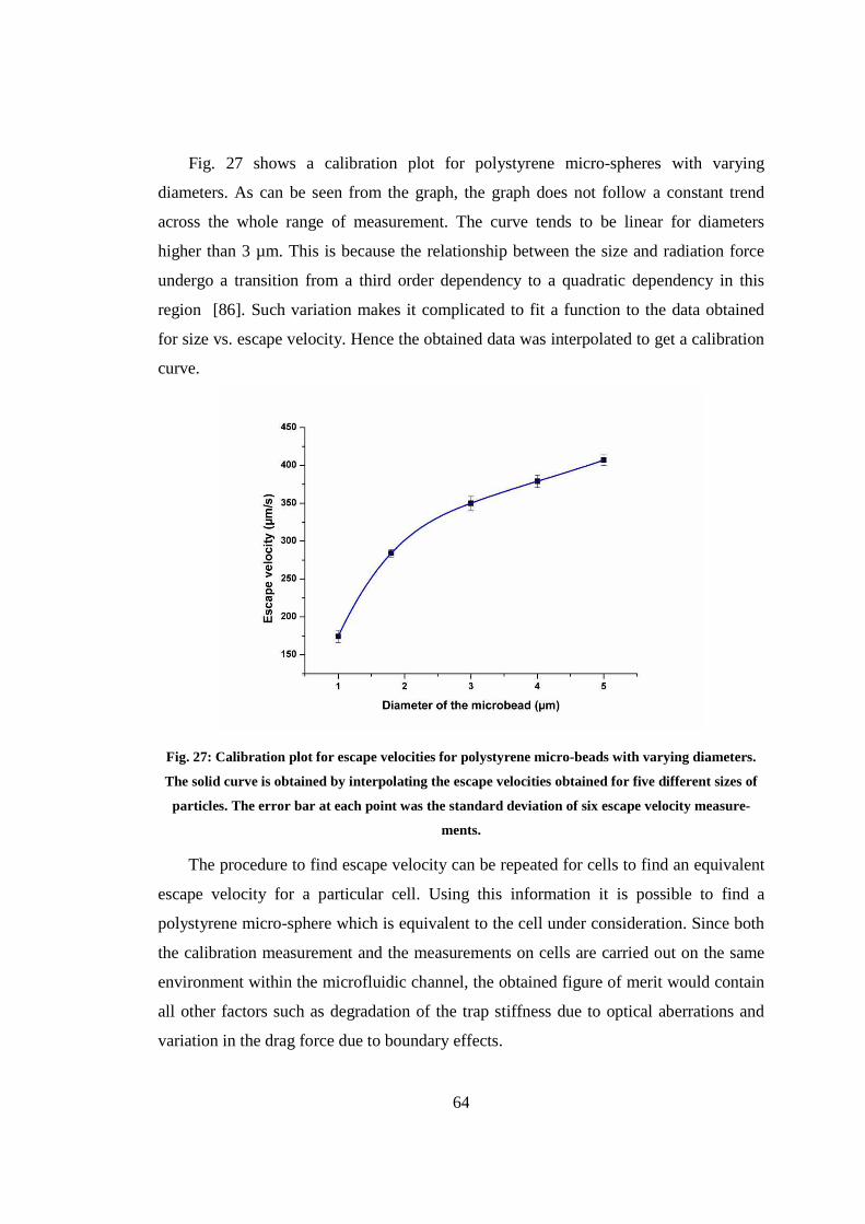
64
Fig. 27 shows a calibration plot for polystyrene micro-spheres with varying
diameters. As can be seen from the graph, the graph does not follow a constant trend
across the whole range of measurement. The curve tends to be linear for diameters
higher than 3 µm. This is because the relationship between the size and radiation force
undergo a transition from a third order dependency to a quadratic dependency in this
region [86]. Such variation makes it complicated to fit a function to the data obtained
for size vs. escape velocity. Hence the obtained data was interpolated to get a calibration
curve.
Fig. 27: Calibration plot for escape velocities for polystyrene micro-beads with varying diameters.
The solid curve is obtained by interpolating the escape velocities obtained for five different sizes of
particles. The error bar at each point was the standard deviation of six escape velocity measure-
ments.
The procedure to find escape velocity can be repeated for cells to find an equivalent
escape velocity for a particular cell. Using this information it is possible to find a
polystyrene micro-sphere which is equivalent to the cell under consideration. Since both
the calibration measurement and the measurements on cells are carried out on the same
environment within the microfluidic channel, the obtained figure of merit would contain
all other factors such as degradation of the trap stiffness due to optical aberrations and
variation in the drag force due to boundary effects.
65
For cell samples, intra species variation in escape velocity might be expected due to
the variation in size and shape of the cells at various stages of its cell cycle. If the
standard deviation of the escape velocities obtained for two cell species are relatively
large in such a way that they overlap, this gives an indication that it would not be
possible to optically fractionate a binary mixture of these cell samples. Thus in situ
calibration measurements can act as an experiment which can be used to determine the
feasibility of optically fractionating two types of cell species. In some cases it would not
be possible to obtain fractionated samples for performing the calibration experiment. In
such cases the feasibility of fractionating such samples may be estimated from a
relatively large (n~100) number of measurements of escape velocity of cells from the
binary mixture. If the distribution of the obtained escape velocities shows a trend of
grouping into two distinct values, it would give an indication that it is possible to
fractionate them.
Once a micro-bead size which is equivalent to a cell species is identified the code
shown in Fig. 25 can be used to find the optimum parameters for performing the
experiment.
Further investigation is required with different cell samples to validate this
procedure and implement this in experiments for passive optical fractionation of cells
using optical landscapes.
4.5 Conclusion
Passive optical sorting of micro-particles using periodic optical landscape has been
proven to be effective and highly sensitive for fractionating micro-particles or nano-
particles [77]. Extending this technology further would be beneficial to develop devices
to achieve passive optical fractionation of cells. Although passive sorting techniques
would not be able to compete with already established active sorting techniques like
FACS, the prospect of achieving label free fractionation of biological particles makes it
a desirable technology. This could open up new opportunities which might have
applications in the field of fundamental biology and biotechnology.
The research discussed in this chapter is a step towards developing such passive
optical sorting technology based on periodic optical landscape. Such a device should be
66
a combination of an optical trapping system with a microfluidic platform. An optical
trapping system, capable of creating a periodic optical landscape using time shared
multiple optical trap was constructed. An acousto-optic deflector was used to obtain
time-shared multiple optical traps. An interface was developed using LabVIEW in order
to control this optical trapping system. This user friendly interface can be used to
generate customized optical landscapes, suitable for optical fractionation experiments.
Although the theory of optical fractionation using periodic optical landscape is well
studied, the theory is based on the assumption that the particle to be sorted is spherical in
shape with known size and refractive index. When it comes to fractionation of cells, this
theory becomes insufficient for cell samples since they generally are non-spherical and
the refractive index and size of the samples are not known. A solution to this issue is
proposed based on in situ calibration, where a spherical micro-particle, whose interaction
with optical trap is similar in a flow when compared to that of a cell. A drag force
measurement can be performed within the microfluidic channel in order to estimate the
escape velocity of a particle from the optical trap. An interpolated calibration curve
obtained from similar measurements for particles of different sizes can be used to find a
spherical micro-bead equivalent to the cell. The results from these measurements may be
used to assess the feasibility of fractionating two types of cells. If it is feasible, the
optimum set of parameters for the device to achieve efficient fractionation may be
obtained.
Further investigations are required for the validation of this technique with various
cellular samples. Once the calibration procedure is completed and the optimum set of
parameters for fractionation is identified, the DA-AOD based optical trapping system
may be used to achieve fractionation of different types of cells flown through a
microfluidic chip. It is also necessary to develop techniques to retrieve fractionated cells
from microfluidic chip. Fractionation efficiency and viability of cells after fractionation
should also be assessed using multi modal approaches.

67
Contributions
P. C. Ashok was trained on the DA-AOD based optical trapping technology by T.
Cizmar. P. C. Ashok built the optical trapping system with the assistance of S. Kagitani.
P. C. Ashok developed the LabVIEW based interface for optical trapping setup. S.
Kagitani wrote the Mathematica code for optimizing the parameters for fractionation
with the assistance of P. C. Ashok. P. C. Ashok developed the idea of in situ calibration
for finding a spherical micro-particle equivalent for cells.
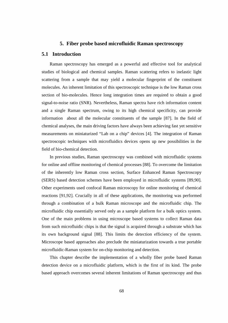
68
5. Fiber probe based microfluidic Raman spectroscopy
5.1 Introduction
Raman spectroscopy has emerged as a powerful and effective tool for analytical
studies of biological and chemical samples. Raman scattering refers to inelastic light
scattering from a sample that may yield a molecular fingerprint of the constituent
molecules. An inherent limitation of this spectroscopic technique is the low Raman cross
section of bio-molecules. Hence long integration times are required to obtain a good
signal-to-noise ratio (SNR). Nevertheless, Raman spectra have rich information content
and a single Raman spectrum, owing to its high chemical specificity, can provide
information about all the molecular constituents of the sample [87]. In the field of
chemical analyses, the main driving factors have always been achieving fast yet sensitive
measurements on miniaturized “Lab on a chip” devices [4]. The integration of Raman
spectroscopic techniques with microfluidics devices opens up new possibilities in the
field of bio-chemical detection.
In previous studies, Raman spectroscopy was combined with microfluidic systems
for online and offline monitoring of chemical processes [88]. To overcome the limitation
of the inherently low Raman cross section, Surface Enhanced Raman Spectroscopy
(SERS) based detection schemes have been employed in microfluidic systems [89,90].
Other experiments used confocal Raman microscopy for online monitoring of chemical
reactions [91,92]. Crucially in all of these applications, the monitoring was performed
through a combination of a bulk Raman microscope and the microfluidic chip. The
microfluidic chip essentially served only as a sample platform for a bulk optics system.
One of the main problems in using microscope based systems to collect Raman data
from such microfluidic chips is that the signal is acquired through a substrate which has
its own background signal [88]. This limits the detection efficiency of the system.
Microscope based approaches also preclude the miniaturization towards a true portable
microfluidic-Raman system for on-chip monitoring and detection.
This chapter describe the implementation of a wholly fiber probe based Raman
detection device on a microfluidic platform, which is the first of its kind. The probe
based approach overcomes several inherent limitations of Raman spectroscopy and thus
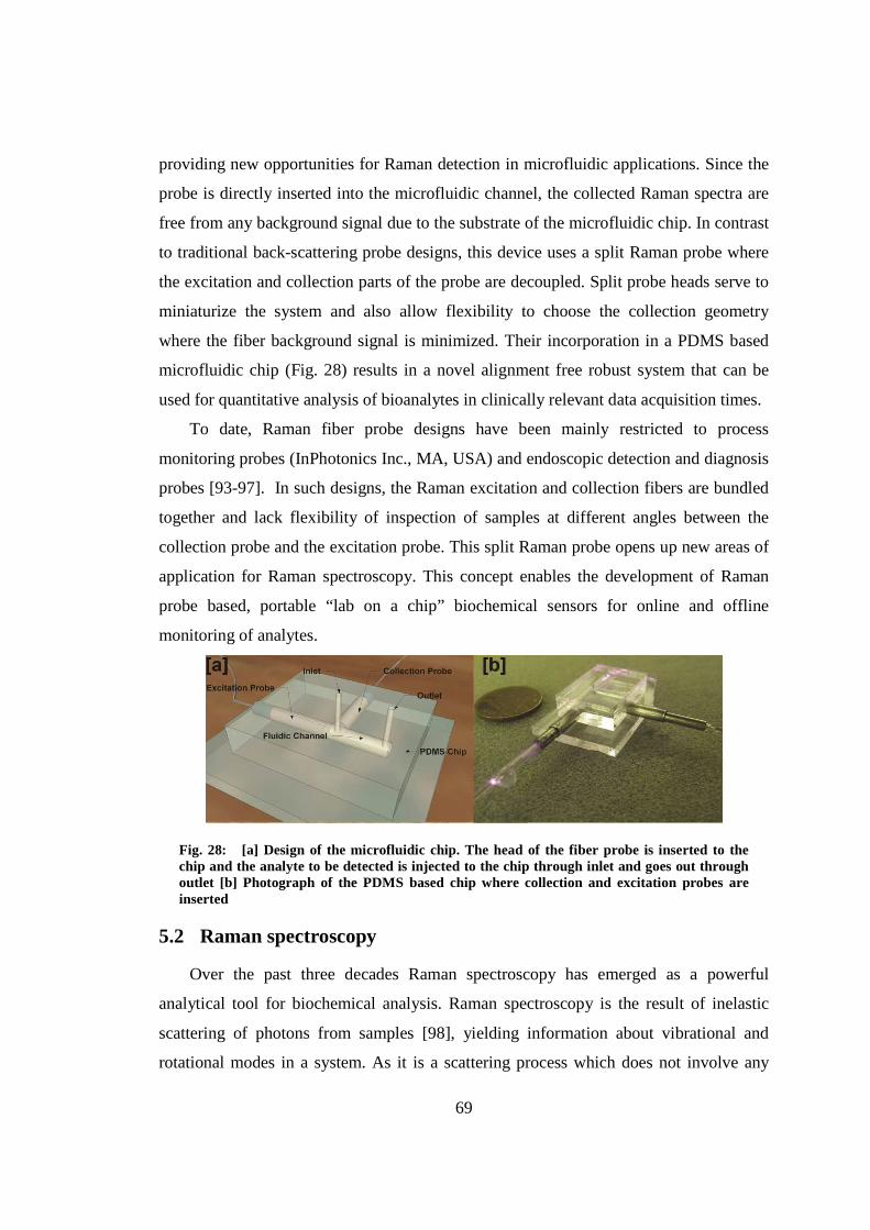
69
providing new opportunities for Raman detection in microfluidic applications. Since the
probe is directly inserted into the microfluidic channel, the collected Raman spectra are
free from any background signal due to the substrate of the microfluidic chip. In contrast
to traditional back-scattering probe designs, this device uses a split Raman probe where
the excitation and collection parts of the probe are decoupled. Split probe heads serve to
miniaturize the system and also allow flexibility to choose the collection geometry
where the fiber background signal is minimized. Their incorporation in a PDMS based
microfluidic chip (Fig. 28) results in a novel alignment free robust system that can be
used for quantitative analysis of bioanalytes in clinically relevant data acquisition times.
To date, Raman fiber probe designs have been mainly restricted to process
monitoring probes (InPhotonics Inc., MA, USA) and endoscopic detection and diagnosis
probes [93-97]. In such designs, the Raman excitation and collection fibers are bundled
together and lack flexibility of inspection of samples at different angles between the
collection probe and the excitation probe. This split Raman probe opens up new areas of
application for Raman spectroscopy. This concept enables the development of Raman
probe based, portable “lab on a chip” biochemical sensors for online and offline
monitoring of analytes.
Fig. 28: [a] Design of the microfluidic chip. The head of the fiber probe is inserted to the chip and the analyte to be detected is injected to the chip through inlet and goes out through outlet [b] Photograph of the PDMS based chip where collection and excitation probes are inserted
5.2 Raman spectroscopy
Over the past three decades Raman spectroscopy has emerged as a powerful
analytical tool for biochemical analysis. Raman spectroscopy is the result of inelastic
scattering of photons from samples [98], yielding information about vibrational and
rotational modes in a system. As it is a scattering process which does not involve any
70
electronic process from the sample such as absorption or fluorescence, Raman
spectroscopy is can be performed irrespective of the electronic energy levels of the
sample of interest. Depending on whether the molecule absorbs energy or loses energy,
Raman process can be divided into Stokes and anti-Stokes Raman process. A vibronic
energy level diagram for the Stokes and anti-Stokes Raman scattering process is shown
in Fig. 29. Since in normal cases, ground state is more populated than excited vibronic
states, Stokes Raman line would be significantly stronger than anti-Stokes lines. Raman
spectra are presented as a Raman shift with respect to the excitation wavelength, and this
shift is expressed in wavenumbers (units of cm-1).
Fig. 29: Energy level diagram of Raman Stokes and anti-Stokes scattering process. “ λexcitation” is the wavelength of the excitation photon, “λRaman” is the wavelength of Raman photon, “∆ω” is the Stokes Raman shift and “E” is the vibrational energy level of the atom or molecule. Raman shift is normally expressed in units of “cm-1”.
According to classical theory, for an incident light of frequency 0υ , the electric field
0 0cos(2 )E E tπυ= will induce dipole moment P as:
[ ]0 0 0 0 0 0 0
0
1cos(2 ) cos2 ( ) cos2 ( )
2 m mP E t q E t tq
αα πυ π υ υ π υ υ ∂= + + + − ∂ (4.1)
Where α is polarisability, q is the nuclear displacement or charge distribution. The
first term of equation 4.1 corresponds to Rayleigh scattered photon of frequency0υ .
Second term corresponds to Raman scattering where, 0( )mυ υ+ would be anti-Stokes
photon and 0( )mυ υ− would be Stokes photon. Equation 4.1 shows that the selection rule
71
for Raman active vibration is that0
0q
α ∂ ≠ ∂ . Which means the rate of change of
polarizability with the vibration must not be zero [99].
The particular advantage of using Raman scattering is that it can be performed at a
range of excitation wavelengths. Thus the excitation pulse can be tuned to consider the
absorption of the analyte and its surroundings, unlike infra-red absorption spectroscopy
which is incompatible with the water-rich environment of biological systems due to the
strong absorption of water in the infra-red region. In contrast to fluorescence
spectroscopy, Raman spectra provide sharp, distinctive Raman peaks corresponding to
the vibrational characteristics of the sample. Through deconvolution of the resulting
spectra it is possible to achieve simultaneous multi-component detection, effectively
giving a “chemical fingerprint” of the composition of the sample of interest [88].
5.3 History of microfluidic Raman spectroscopy
It has been over a decade since Raman spectroscopy was being used as a potential
detection tool for analyzing samples in microfluidic systems [100]. Since then several
groups demonstrated the power of Raman spectroscopy as a potential optical detection
tool to interrogate samples in microfluidic chips. Later years saw a wide variety of
applications which resulted from the marriage of these two powerful technologies. The
reviews by Viskari and Landers (2006) [88] and Hunt and Wilkinson (2008) [14] discuss
the implementation of Raman spectroscopy as a potential optical detection technique in
microfluidics. Microfluidic Raman Spectroscopy (MRS) has seen variants of its
implementation in terms of different microfluidic architectures and different Raman
spectroscopic techniques such as normal Raman spectroscopy, confocal Raman
spectroscopy, resonance Raman spectroscopy, and SERS [88]. Here, various relevant
studies are presented in the correct context and in a chronological order to illustrate the
relevance of these works in the advancement of the field of MRS. A special emphasis is
given to each study on the various microfluidic architectures and Raman detection
schemes adopted for the implementation of this technology for bio-chemical analysis.
72
5.3.1 Initial studies
Since the late 1980s, there have been several papers where microcapillary based
electrophoretic systems were interrogated with Raman spectroscopy [101,102]. A similar
approach was used to analyze isotachophoretically concentrated ribonucleotides [100].
The capillaries however had limited surface area, reducing the sensitivity of detection.
The alignment requirement was also higher for mounting a capillary on a conventional
Raman microscope. These issues led to the implementation of a microchip based version
of the same separation technique, in which on-chip Raman spectroscopy of
isotachophoretically separated herbicides - paraquat and diquat – was achieved [103]. In
this work, a glass microfluidic chip was coupled to a free space Raman microprobe;
more efficient collection of Raman signal could be achieved with reduced background
from the glass by carefully choosing the thickness of the coverslip under the microchip.
This study envisages the opportunities for further enhancement of sensitivity by
implementing SERS or resonant Raman spectroscopy.
In a later study, time resolved resonance Raman spectroscopy (TR3) was employed
within a glass microfluidic chip to study chromophore structure [104,105]. This study
was achieved through miniaturization of the standard rapid flow technique used to study
photochemical kinetics and combining it with Raman spectroscopic detection. The
standard rapid flow technique was performed using a macro flow device, requiring high
amounts of pigments at high flow rates. The implementation of a microfluidic version of
the device reduced the required sample volume by shrinking the fluidic channel to match
the confocal volume of the Raman detection system.
The pioneering work on the implementation of SERS in microfluidics was the
detection of a derivative of trinitrotoluene (TNT) in a glass microfluidic chip using
surface enhanced resonance Raman spectroscopy (SERRS) [106]. In this device, on-chip
preparation of silver colloid was achieved which was further mixed with the sample to
be detected followed by detection of SERRS. The microfluidic chip allowed a reduction
of the required reagent volume and the sensitivity was improved by two orders of
magnitude by using SERRS compared to macro flow cells. In addition the long term
stability of the flow stream, offered by the microfluidic channel, allowed accumulation
of signal for a longer duration.
73
5.3.2 Raman spectroscopy to probe reactions
The field of microfluidics enables real-time study of chemical reactions through
micro-reactors using reduced volumes of reagents. This enables optimization of various
parameters, which is essential for efficient large scale commercial production of
chemicals. Various detection methods – thermal, electrical and optical - have been
combined with micro-reactor based microfluidic chips to probe the temporal and spatial
evolution of a chemical reaction. The ability for Raman spectroscopy to perform
simultaneous multi-component detection makes it a desirable method to monitor the
progress of a reaction within a micro-reactor. There have been several architectures to
integrate Raman detection in micro-reactors for temporal and spatial mapping of the
chemical composition of the sample in micro-reactors. The formation of diazonium salts
in anhydrous conditions and their subsequent chlorination in situ was studied using on-
line, on-chip Raman spectroscopy by probing a glass based microfluidic reactor using a
Raman microscope [107]. Another reported study looked at spatially mapping the
evolution of the reaction to form ethyl acetate from ethanol and acetic acid in a Pyrex
glass based microfluidic chip using a confocal Raman microscope [108]. It was observed
in this work that resonance Raman spectroscopy or SERS should be employed to
enhance the sensitivity and reduce the acquisition time to achieve real-time monitoring
of the reaction. The applicability of MRS in micro-reactors was further extended to
studies of biologically relevant processes such as enzyme catalyzed enzyme catalyzed
reactions for the synthesis of peptides from amino acids [109].
The first use of PDMS based microfluidic chips in conjunction with Raman
spectroscopic probing was to study the mixing of ethanol and isopropanol using
Confocal Raman microscopy [110]. Since PDMS is a polymer, it is highly Raman active
and there are specific Raman lines due to PDMS in the fingerprint region. This work
discusses the issues associated with the background signals from PDMS unless a
confocal configuration is used for Raman detection. MRS for reaction optimization was
further taken forward for studying various reaction dynamics with a variety of
microfluidic architectures. This included designing specialized micromixers to enhance
the efficiency of mixing dynamics [92,111] .
74
In addition to its use in studying chemical reactions, MRS has also been employed
to study fluid dynamics. The diffusion of two miscible, non-reacting liquids was studied
in a silicon glass based microfluidic chip [112]. Confocal Raman spectroscopy was used
to probe the interdiffusion of chloroform, dimethlysulfoxide, acetonitrile and
dimethlyformamide. The obtained data was used to estimate the diffusion coefficients of
the liquids. Through their approach, the authors envisage exploiting the multi-
component detection ability of Raman spectroscopy to probe the interdiffusion of more
than two liquids or situations where multiple chemical reactions occur simultaneously.
5.3.3 Bio-chemical detection using SERS microfluidics
SERS based detection is widely used to overcome the low cross section of the
Raman process and has additionally found a variety of implementations in MRS. The
feasibility of combining microfluidic separation devices with SERS was demonstrated
by integrating metal-polymer nanocomposite in a PDMS microfluidic chip and
collecting SERS spectra using a confocal Raman microscope [89]. A mixture of
riboflavin and resorufin was detected as a proof of principle to demonstrate the
combination of a powerful separation technique (capillary electrophoresis) with a
structurally information rich analytical technique (Raman spectroscopy).
Further, the feasibility of using the multi-component detection ability of Raman
spectroscopy in microfluidics was demonstrated by several groups who demonstrated the
detection of a mixture of dye labeled oligonucleotides through multiplexed SERRS
detection in a PDMS microfluidic chip [113,114]. These enabled highly sensitive SERS
detection on a microfluidic platform. The microfluidic architecture has also seen
improvement, several groups have used PDMS chips with alligator teeth-like structures
for the efficient mixing of colloids with samples for SERS detection [115,114]. In
addition to colloidal based SERS detection, there have been attempts to develop efficient
SERS substrates in PDMS which could be used to obtain reproducible SERS spectra of
bio-molecules.
Although SERS based detection offers high sensitivity and proves efficient for qualita-
tive chemical analysis, quantitative analysis of chemicals using SERS is not easy to
achieve as it is difficult to control various experimental parameters including degree of
75
aggregation, particle sizes of colloidal nanoparticles and distribution of molecules on a
metal surface. The sample manipulation capability offered by microfluidics however
makes it possible to achieve quantitative studies in SERS-based MRS. With specially
fabricated three-dimensional micromixers for efficient sample mixing with colloids,
several groups have demonstrated quantitative SERS detection of samples [116,117].
Unlike previous microfluidic SERS embodiments, where Raman measurements were
taken in a static condition [113], it was observed that the reproducibility is better in a
flow mode [116]. The success in the implementation of SERS based LoC devices
enabled researchers to use this as a technique to standardize the detection achieved
through other methods. In one study, confocal SERS detection was used to complement
the fluorescence resonance energy transfer (FRET) data of DNA hybridization in a
PDMS based microfluidic system [118]. An exhaustive discussion on the implementa-
tion of SERS in microfluidics may be found in the review by Chen and Choo [119].
5.3.4 Raman spectroscopic probing of microdroplets
Microfluidic devices that can generate sub-nanoliter microdroplets, dispersed within
an immiscible continuous phase of oil in a rapid, efficient and controllable manner is
gaining attention of the analytical community for a wide range of applications [120].
Microdroplet based microfluidic systems are preferred for bio-chemical reactions and
analysis as the compartmentalization provides the advantage of keeping the reactants or
the sample isolated. Microdroplets are of particular interest to biologists as it is possible
to mimic a cell like system within a microdroplet for genomics, proteomics or system
biology studies [120].
There have been a number of reported works where Raman spectroscopy was used
to probe the samples in microdroplets generated in a microfluidic system. In one of the
first reported studies, a microdroplet based micro-reactor was implemented in a PDMS
chip and confocal Raman spectroscopy was used to probe the microdroplets [121]. It
was observed that the droplet based micro-reactors are ideal as they can host a rapid
exothermal chemical reaction in a controlled condition. In situ probing of the
composition of the droplets was achieved using Raman spectroscopy and the mixing
dynamics within the droplets were studied. However, acquisition time was high to
76
achieve sufficient sensitivity for probing the sample; hence multiple droplets would pass
through the interrogation region during an acquisition, giving only the average signal of
several droplets. There was also interference in the spectra from the oil phase which had
to be subtracted when post-processing the spectra. Another embodiment of microdroplet
based MRS studied on-chip photo-polymerization of benzyl methacrylate in a
borosilicate glass based microfluidic device using a low resolution Raman system. In
this study, a fiber probe was used instead of an objective to excite and collect the Raman
signal [122]. However, its comparatively long acquisition time (3 minutes) made this
system unsuitable for online monitoring of the process.
To avoid issues of sensitivity and background from the oil, SERS detection has been
combined with a microdroplet based glass microfluidic system [123]. Samples mixed
with gold colloids were sequestered in microdroplets and SERS signals were acquired
with an acquisition time of 1s. Such a detection scheme has potential in process
diagnostics in which online detection of drugs, water pollutants or food additives is
required. Microdroplets dynamics were studied using confocal Raman spectroscopy by
monitoring the isotopic exchange reaction between D2O and H2O [124]. Even though the
comparatively long acquisition time created issues with obtaining average signals from
multiple droplets, this system was used to study interdiffusion mixing and droplet
mixing within a microfluidic channel through spatially resolved concentration maps of
the sample.
5.3.5 Microfluidic Raman spectroscopy in cell science
The use of microfluidic systems for cell biology research is a rapidly growing area
of research [125]. The main use of microfluidic systems in cell biology is to obtain
chemical information of cells and tissues at a molecular level. The ability of Raman
spectroscopy to probe the molecular fingerprint of a sample makes it highly desirable for
it to be combined with microfluidics to answer fundamental questions in cell biology.
The relatively long acquisition times required in Raman spectroscopy (typically from a
few seconds to several minutes) makes it necessary to have a tool which can non-
invasively hold the cell within the microfluidic channel, away from the fluidic channel
walls, while Raman spectra are acquired. A solution to this is to use optical tweezers
77
which has a proven track record for its ability in single cell manipulation [126].
Interestingly, the combination of optical tweezers with micro-Raman spectroscopy has
developed as a field of its own, finding a variety of applications in the area of
biophotonics [127]. The combination of micro-Raman tweezers technology with
microfluidics has proven to be a powerful technology where microfluidics adds the
advantage of providing a more controlled environment for single cell studies.
One of the first attempts to combine micro-Raman tweezers with microfluidics was
for the study of the oxygenation cycle of red blood cells (RBC) [91]. A single RBC was
trapped in a PDMS based microfluidic chip and the oxygenation cycle of hemoglobin
with respect to the surrounding environment was studied through confocal resonance
Raman spectroscopy. The same group used this system for further studies of protein
denaturation in RBC [128] and for studies of several globin containing cells, where in
vivo conditions were mimicked in a microfluidic channel [129]. In another study, a
PDMS based microfluidic system was combined with a dual beam fiber optical trap to
trap HL60 human Promyelocytic leukemia cells, and a confocal Raman system was used
to record Raman spectra of the cells [130]. In another study, in situ chemical
characterization of Chinese Hamster Ovary cells (CHO-K1) with spatial and temporal
resolution was achieved by recording SERS of immobilized cells mixed with gold
nanoparticles in a microfluidic channel using a confocal Raman microscope [131].
The prospect of obtaining Raman spectra of single cell in a flow based microfluidic
system, in combination with micro-Raman tweezers, offers the opportunity to develop
Raman activated microfluidic cell sorting devices. Such a system was realized in which
sorting of leukemia cells was demonstrated as a proof of principle. In this study, optical
tweezers trapped the cells, the Raman signals of which were acquired by a confocal
Raman microscope [74]. After analyzing the Raman spectra, the optical tweezers moved
the cell towards the corresponding sorted channel. However this technique had very low
throughput due to relatively long Raman acquisition time.
5.3.6 Recent Developments
The ultimate goal of lab on a chip technology is to create analytical devices that are
portable so that they can be used for point-of-care testing and field analysis. This makes
78
miniaturization of MRS devices important. In a recently reported study, a microfluidic
system for confocal SERS detection of dipicolnic acid and malachite green was realized
[90]. Specially fabricated micro-pillars on the PDMS chip were used to achieve efficient
mixing of colloidal nanoparticles with the sample. The notable achievement of this work
was the implementation of the detection on a benchtop Raman microscope. This is an
important step forward towards developing MRS devices for real field test applications.
In all of the previously mentioned studies, conventional Raman microscopes were
used to record Raman spectra from the microfluidic channels using high numerical
aperture objectives. A recently reported study looked into the aspects of optimizing
Raman signal collection from microfluidic channels [132]. In this work, a glass based
micro-reactor was used to probe the acid catalyzed esterification of butanol with acetic
anhydride to produce butyl acetate and acetic acid. It was shown that for a non-confocal
setup, a miniature aspheric lens would be better than a high numerical aperture
microscope objective to collect Raman spectra from the sample in the microfluidic
channels. This paper contains a detailed discussion regarding the issues that can arise
when detecting Raman signals from a microfluidic chip. The relatively high power of
excitation (100s of mW) needed to overcome the low Raman cross section issue can
create localized heating which can affect the reaction dynamics. This issue would be
serious when high numerical aperture objectives are used to collect the Raman signal
since the Raman excitation beam is tightly focused to a very small volume resulting in
relatively high power density at the focal spot. The refractive index change induced by
photo-thermal effects can affect the collection efficiency. There may also be the creation
of bubbles inside the microfluidic channels due to cavitation, which would disrupt the
flow inside the microfluidic channel. Another issue is the localized imperfections on the
substrate that might affect the quality of the acquired data. These impurities would
introduce unwanted fluorescence background which is difficult to remove through
processing.
5.4 Fiber probe based microfluidic Raman spectroscopy – Rationale
Embedding optical waveguides such as optical fibers is a route to the manufacture
of microfluidic chips which incorporate optical detection schemes while retaining
79
portability and eliminating the need for optical alignment. This also helps to minimize
the number of required optical components [133]. This approach has been successfully
implemented for various optical detection methods. However, implementation of fiber
based Raman spectroscopic detection schemes in microfluidics was not exploited until
recently due to practical difficulties.
To understand explain this issue, it is worthwhile exploring how fiber based
detection schemes were implemented for other spectroscopic methods. In one of the first
studies, a fiber based on-chip fluorescent excitation was used in microfluidics. A fiber
insertion channel was etched into the microfluidic chip in such a way that the tip of the
fiber, when fiber was inserted in the fiber insertion channel, would remain 190 µm away
from the fluidic channel [134]. In a recently reported study, on chip absorption
spectroscopy was implemented using optical fiber based excitation and collection for
high throughput cell screening [135]. As before, the fiber insertion channel is separated
from the fluidic channel by a wall.
When embedded fiber probes are used for optical detection in microfluidic chips,
there was a wall separating the fiber tip within its insertion channel from the fluidic
channel through which the analyte flows. This approach is not desirable for a fiber based
Raman detection scheme in microfluidics as there will be interfering signal from the
substrate. A modified microfluidic design is required to implement fiber based Raman
detection in microfluidics such that the fiber probe is embedded in a chip without walls
that physically separate the tip of the probe from the fluidic channel.
Due to the inherent characteristics of Raman spectroscopy, a slightly different
approach is necessary when implementing fiber based Raman systems. Due to the low
Raman cross section, it is essential to enhance the collection efficiency and to reduce the
fluorescence background to achieve satisfactory detection sensitivity. There can be
significant fluorescence contribution from the optical fiber itself when Raman excitation
beam gets guided through it. To reduce this background, low OH (hydroxyl) optical
fibers are used for near IR applications. Also unlike other spectroscopic probes,
specialized filters must be introduced at the probe head so as to filter out the fluorescent
background from the excitation fiber and to prevent Rayleigh scattered photons being
directed into the collection fiber [94].
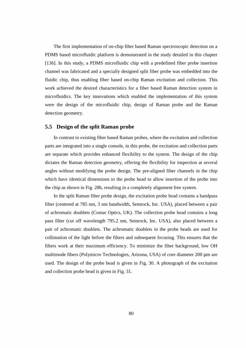
80
The first implementation of on-chip fiber based Raman spectroscopic detection on a
PDMS based microfluidic platform is demonstrated in the study detailed in this chapter
[136]. In this study, a PDMS microfluidic chip with a predefined fiber probe insertion
channel was fabricated and a specially designed split fiber probe was embedded into the
fluidic chip, thus enabling fiber based on-chip Raman excitation and collection. This
work achieved the desired characteristics for a fiber based Raman detection system in
microfluidics. The key innovations which enabled the implementation of this system
were the design of the microfluidic chip, design of Raman probe and the Raman
detection geometry.
5.5 Design of the split Raman probe
In contrast to existing fiber based Raman probes, where the excitation and collection
parts are integrated into a single console, in this probe, the excitation and collection parts
are separate which provides enhanced flexibility to the system. The design of the chip
dictates the Raman detection geometry, offering the flexibility for inspection at several
angles without modifying the probe design. The pre-aligned fiber channels in the chip
which have identical dimensions to the probe head to allow insertion of the probe into
the chip as shown in Fig. 28b, resulting in a completely alignment free system.
In the split Raman fiber probe design, the excitation probe head contains a bandpass
filter (centered at 785 nm, 3 nm bandwidth, Semrock, Inc. USA), placed between a pair
of achromatic doublets (Comar Optics, UK). The collection probe head contains a long
pass filter (cut off wavelength 795.2 nm, Semrock, Inc. USA), also placed between a
pair of achromatic doublets. The achromatic doublets in the probe heads are used for
collimation of the light before the filters and subsequent focusing. This ensures that the
filters work at their maximum efficiency. To minimize the fiber background, low OH
multimode fibers (Polymicro Technologies, Arizona, USA) of core diameter 200 µm are
used. The design of the probe head is given in Fig. 30. A photograph of the excitation
and collection probe head is given in Fig. 31.
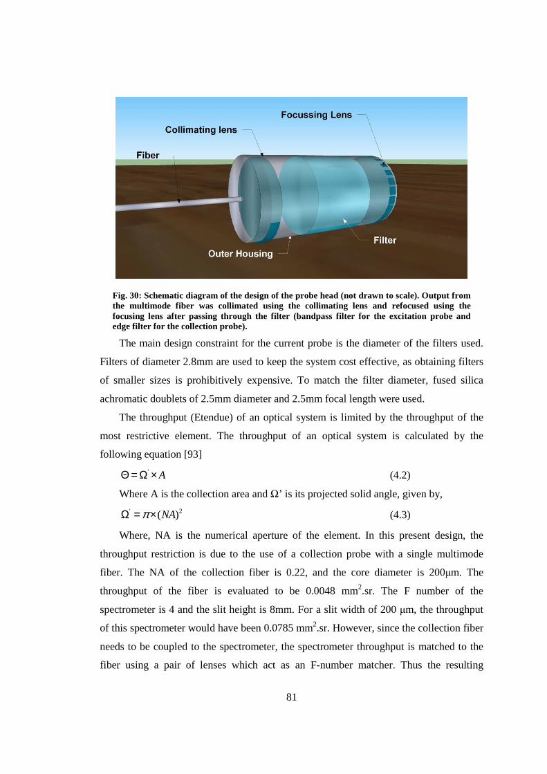
81
Fig. 30: Schematic diagram of the design of the probe head (not drawn to scale). Output from the multimode fiber was collimated using the collimating lens and refocused using the focusing lens after passing through the filter (bandpass filter for the excitation probe and edge filter for the collection probe).
The main design constraint for the current probe is the diameter of the filters used.
Filters of diameter 2.8mm are used to keep the system cost effective, as obtaining filters
of smaller sizes is prohibitively expensive. To match the filter diameter, fused silica
achromatic doublets of 2.5mm diameter and 2.5mm focal length were used.
The throughput (Etendue) of an optical system is limited by the throughput of the
most restrictive element. The throughput of an optical system is calculated by the
following equation [93]
' AΘ = Ω × (4.2)
Where A is the collection area and Ω’ is its projected solid angle, given by,
' 2( )NAπΩ = × (4.3)
Where, NA is the numerical aperture of the element. In this present design, the
throughput restriction is due to the use of a collection probe with a single multimode
fiber. The NA of the collection fiber is 0.22, and the core diameter is 200µm. The
throughput of the fiber is evaluated to be 0.0048 mm2.sr. The F number of the
spectrometer is 4 and the slit height is 8mm. For a slit width of 200 µm, the throughput
of this spectrometer would have been 0.0785 mm2.sr. However, since the collection fiber
needs to be coupled to the spectrometer, the spectrometer throughput is matched to the
fiber using a pair of lenses which act as an F-number matcher. Thus the resulting
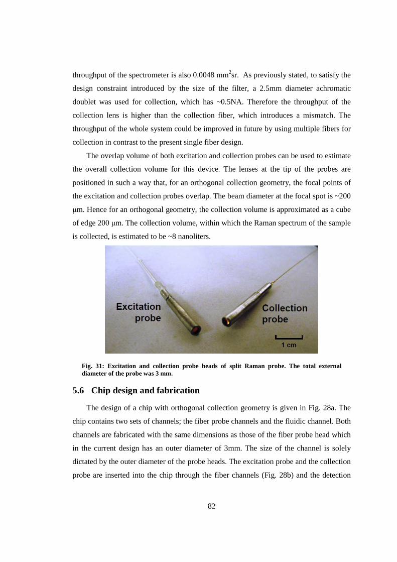
82
throughput of the spectrometer is also 0.0048 mm2sr. As previously stated, to satisfy the
design constraint introduced by the size of the filter, a 2.5mm diameter achromatic
doublet was used for collection, which has ~0.5NA. Therefore the throughput of the
collection lens is higher than the collection fiber, which introduces a mismatch. The
throughput of the whole system could be improved in future by using multiple fibers for
collection in contrast to the present single fiber design.
The overlap volume of both excitation and collection probes can be used to estimate
the overall collection volume for this device. The lenses at the tip of the probes are
positioned in such a way that, for an orthogonal collection geometry, the focal points of
the excitation and collection probes overlap. The beam diameter at the focal spot is ~200
µm. Hence for an orthogonal geometry, the collection volume is approximated as a cube
of edge 200 µm. The collection volume, within which the Raman spectrum of the sample
is collected, is estimated to be ~8 nanoliters.
Fig. 31: Excitation and collection probe heads of split Raman probe. The total external diameter of the probe was 3 mm.
5.6 Chip design and fabrication
The design of a chip with orthogonal collection geometry is given in Fig. 28a. The
chip contains two sets of channels; the fiber probe channels and the fluidic channel. Both
channels are fabricated with the same dimensions as those of the fiber probe head which
in the current design has an outer diameter of 3mm. The size of the channel is solely
dictated by the outer diameter of the probe heads. The excitation probe and the collection
probe are inserted into the chip through the fiber channels (Fig. 28b) and the detection
83
analyte is flowed through the fluidic channel. The physical dimensions of the chip with
inserted probe heads is 25mm×30mm.
The microfluidic chip is fabricated with PDMS using conventional soft lithographic
techniques [7]. The mold for the chip is fabricated by adhering 3mm metallic sleeves
onto a glass substrate using a medical epoxy (Loctite M-31CL Hysol), which defines the
probe entrance channel and fluidic channel. This makes it possible to insert the probe
into the chip conveniently and the channel design ensures the relative alignment of
excitation probe to the collection probe. In principle, with this same approach, it is
possible to reduce the channel size to the order of 100µm. Hence the same fabrication
method may readily be extended to fabricate chips of smaller footprints.
5.7 Detection device
Fig. 32 illustrates the portable microfluidic Raman detection system. A laser power
of 200 mW from a 785nm diode laser (Laser2000 (UK) Ltd.) was used for Raman
excitation at exit of the excitation probe head. The Raman excitation and the collection
probes are coupled to the laser and the spectrometer (Shamrock SR-303i, Andor
Technology) respectively using SMA connectors (Thorlabs Inc., USA). The
spectrometer employs a 400 lines/mm grating, blazed at 850 nm and is equipped with a
deep depletion, back-illuminated and thermoelectrically cooled CCD camera (Newton,
Andor Technology) for the detection of Raman signal. The resolution of the Raman
system is measured by the FWHM of the Silicon Raman peak at 520 cm-1 and is found to
be better than 6 cm-1.
The physical dimension of the whole system including the PDMS chip, Raman
probe, laser source, spectrometer and CCD is 60cm × 35cm × 25cm. The physical
dimensions and also the alignment free nature of this fiber probe based system make it a
portable device. The probe based approach gives flexibility to the system enabling it
reach otherwise inaccessible areas, a feature which has potential applications in online
monitoring of the samples.
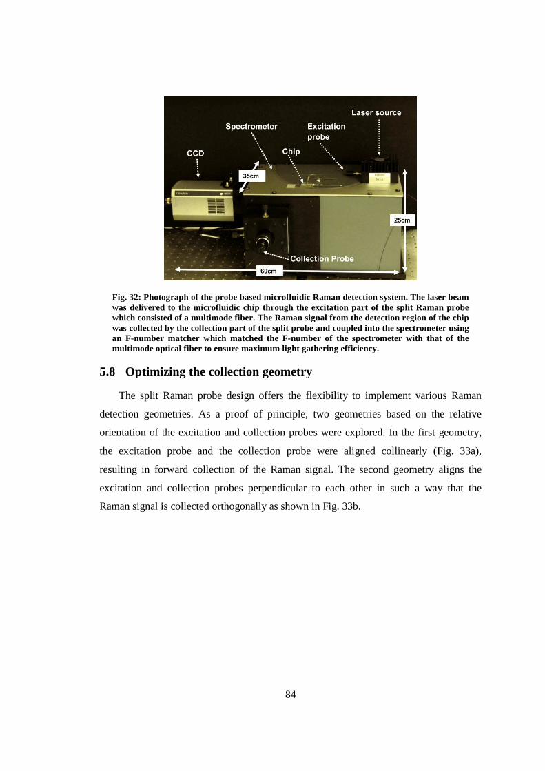
84
Fig. 32: Photograph of the probe based microfluidic Raman detection system. The laser beam was delivered to the microfluidic chip through the excitation part of the split Raman probe which consisted of a multimode fiber. The Raman signal from the detection region of the chip was collected by the collection part of the split probe and coupled into the spectrometer using an F-number matcher which matched the F-number of the spectrometer with that of the multimode optical fiber to ensure maximum light gathering efficiency.
5.8 Optimizing the collection geometry
The split Raman probe design offers the flexibility to implement various Raman
detection geometries. As a proof of principle, two geometries based on the relative
orientation of the excitation and collection probes were explored. In the first geometry,
the excitation probe and the collection probe were aligned collinearly (Fig. 33a),
resulting in forward collection of the Raman signal. The second geometry aligns the
excitation and collection probes perpendicular to each other in such a way that the
Raman signal is collected orthogonally as shown in Fig. 33b.
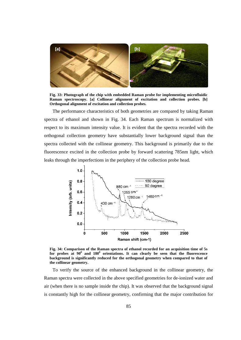
85
Fig. 33: Photograph of the chip with embedded Raman probe for implementing microfluidic Raman spectroscopy. [a] Collinear alignment of excitation and collection probes. [b] Orthogonal alignment of excitation and collection probes.
The performance characteristics of both geometries are compared by taking Raman
spectra of ethanol and shown in Fig. 34. Each Raman spectrum is normalized with
respect to its maximum intensity value. It is evident that the spectra recorded with the
orthogonal collection geometry have substantially lower background signal than the
spectra collected with the collinear geometry. This background is primarily due to the
fluorescence excited in the collection probe by forward scattering 785nm light, which
leaks through the imperfections in the periphery of the collection probe head.
Fig. 34: Comparison of the Raman spectra of ethanol recorded for an acquisition time of 5s for probes at 900 and 1800 orientations. It can clearly be seen that the fluorescence background is significantly reduced for the orthogonal geometry when compared to that of the collinear geometry.
To verify the source of the enhanced background in the collinear geometry, the
Raman spectra were collected in the above specified geometries for de-ionized water and
air (when there is no sample inside the chip). It was observed that the background signal
is constantly high for the collinear geometry, confirming that the major contribution for
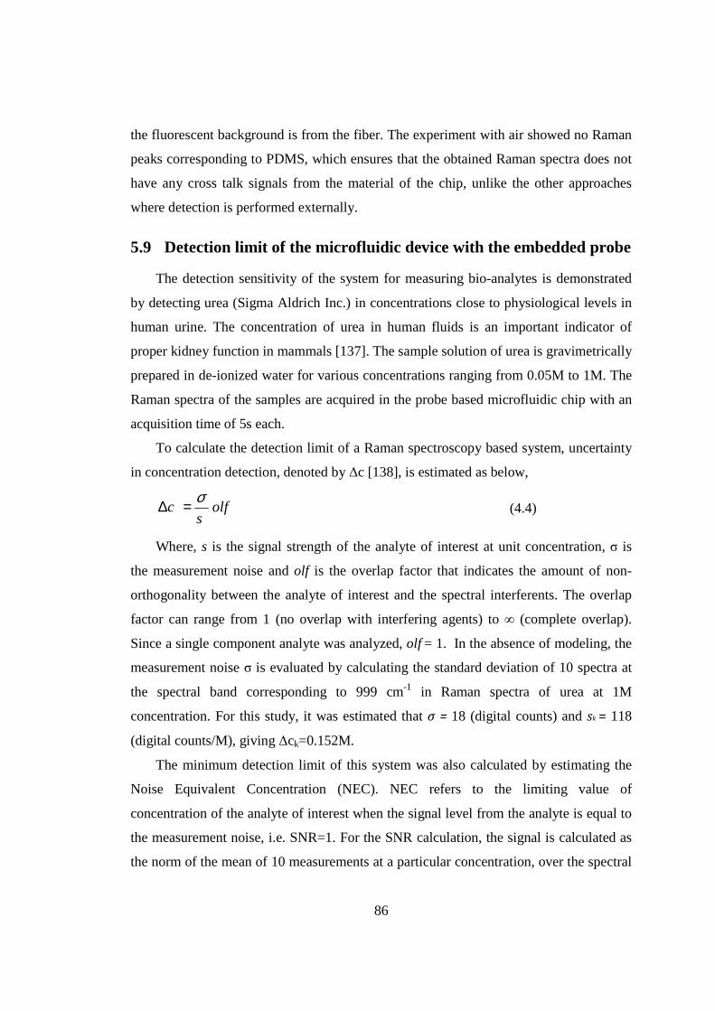
86
the fluorescent background is from the fiber. The experiment with air showed no Raman
peaks corresponding to PDMS, which ensures that the obtained Raman spectra does not
have any cross talk signals from the material of the chip, unlike the other approaches
where detection is performed externally.
5.9 Detection limit of the microfluidic device with the embedded probe
The detection sensitivity of the system for measuring bio-analytes is demonstrated
by detecting urea (Sigma Aldrich Inc.) in concentrations close to physiological levels in
human urine. The concentration of urea in human fluids is an important indicator of
proper kidney function in mammals [137]. The sample solution of urea is gravimetrically
prepared in de-ionized water for various concentrations ranging from 0.05M to 1M. The
Raman spectra of the samples are acquired in the probe based microfluidic chip with an
acquisition time of 5s each.
To calculate the detection limit of a Raman spectroscopy based system, uncertainty
in concentration detection, denoted by ∆c [138], is estimated as below,
c olfs
σ∆ = (4.4)
Where, s is the signal strength of the analyte of interest at unit concentration, σ is
the measurement noise and olf is the overlap factor that indicates the amount of non-
orthogonality between the analyte of interest and the spectral interferents. The overlap
factor can range from 1 (no overlap with interfering agents) to ∞ (complete overlap).
Since a single component analyte was analyzed, olf = 1. In the absence of modeling, the
measurement noise σ is evaluated by calculating the standard deviation of 10 spectra at
the spectral band corresponding to 999 cm-1 in Raman spectra of urea at 1M
concentration. For this study, it was estimated that σ = 18 (digital counts) and sk = 118
(digital counts/M), giving ∆ck=0.152M.
The minimum detection limit of this system was also calculated by estimating the
Noise Equivalent Concentration (NEC). NEC refers to the limiting value of
concentration of the analyte of interest when the signal level from the analyte is equal to
the measurement noise, i.e. SNR=1. For the SNR calculation, the signal is calculated as
the norm of the mean of 10 measurements at a particular concentration, over the spectral
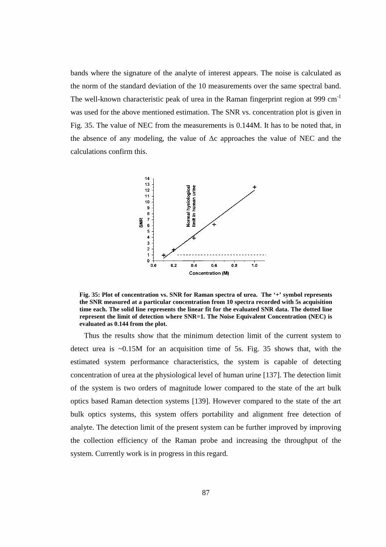
87
bands where the signature of the analyte of interest appears. The noise is calculated as
the norm of the standard deviation of the 10 measurements over the same spectral band.
The well-known characteristic peak of urea in the Raman fingerprint region at 999 cm-1
was used for the above mentioned estimation. The SNR vs. concentration plot is given in
Fig. 35. The value of NEC from the measurements is 0.144M. It has to be noted that, in
the absence of any modeling, the value of ∆c approaches the value of NEC and the
calculations confirm this.
Fig. 35: Plot of concentration vs. SNR for Raman spectra of urea. The ‘+’ symbol represents the SNR measured at a particular concentration from 10 spectra recorded with 5s acquisition time each. The solid line represents the linear fit for the evaluated SNR data. The dotted line represent the limit of detection where SNR=1. The Noise Equivalent Concentration (NEC) is evaluated as 0.144 from the plot.
Thus the results show that the minimum detection limit of the current system to
detect urea is ~0.15M for an acquisition time of 5s. Fig. 35 shows that, with the
estimated system performance characteristics, the system is capable of detecting
concentration of urea at the physiological level of human urine [137]. The detection limit
of the system is two orders of magnitude lower compared to the state of the art bulk
optics based Raman detection systems [139]. However compared to the state of the art
bulk optics systems, this system offers portability and alignment free detection of
analyte. The detection limit of the present system can be further improved by improving
the collection efficiency of the Raman probe and increasing the throughput of the
system. Currently work is in progress in this regard.
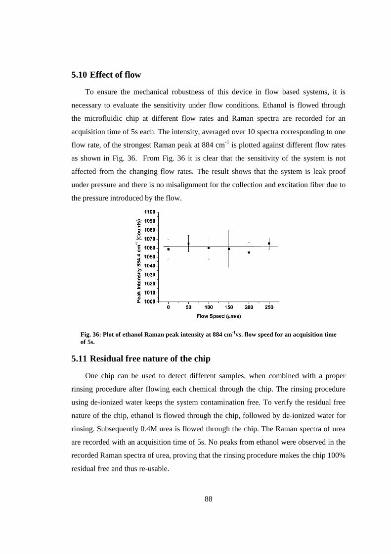
88
5.10 Effect of flow
To ensure the mechanical robustness of this device in flow based systems, it is
necessary to evaluate the sensitivity under flow conditions. Ethanol is flowed through
the microfluidic chip at different flow rates and Raman spectra are recorded for an
acquisition time of 5s each. The intensity, averaged over 10 spectra corresponding to one
flow rate, of the strongest Raman peak at 884 cm-1 is plotted against different flow rates
as shown in Fig. 36. From Fig. 36 it is clear that the sensitivity of the system is not
affected from the changing flow rates. The result shows that the system is leak proof
under pressure and there is no misalignment for the collection and excitation fiber due to
the pressure introduced by the flow.
Fig. 36: Plot of ethanol Raman peak intensity at 884 cm-1vs. flow speed for an acquisition time of 5s.
5.11 Residual free nature of the chip
One chip can be used to detect different samples, when combined with a proper
rinsing procedure after flowing each chemical through the chip. The rinsing procedure
using de-ionized water keeps the system contamination free. To verify the residual free
nature of the chip, ethanol is flowed through the chip, followed by de-ionized water for
rinsing. Subsequently 0.4M urea is flowed through the chip. The Raman spectra of urea
are recorded with an acquisition time of 5s. No peaks from ethanol were observed in the
recorded Raman spectra of urea, proving that the rinsing procedure makes the chip 100%
residual free and thus re-usable.
89
5.12 Conclusions
Combining various optical detection techniques into a microfluidic platform has
always been a technical challenge. However, optical detection and manipulation
techniques play a crucial role in the development of the field of microfluidics. Although
there have been several demonstration of the use of optical detection techniques on a
microfluidic platforms, the majority of these were limited to laboratory based systems.
To translate these technologies into devices suitable for field applications, it is essential
to make the optical detection part of the system completely alignment free and portable.
As discussed in Chapter 3, one approach towards achieving this is to use an embedded
fiber based waveguide for optical signal delivery and collection from the microfluidic
chip.
This chapter has detailed the realization of a fiber probe based microfluidic Raman
sensor. The chapter starts with a brief history of the implementation of Raman
spectroscopy in conjunction with microfluidics and its evolution over last decade. The
work mentioned in this chapter can be considered as a transition of microfluidic Raman
spectroscopic technique from free-space bulk optical systems to fiber based alignment-
free systems. The capability of a novel fiber probe based microfluidic Raman sensor to
be used for qualitative and quantitative analysis was demonstrated. This device was
realized by embedding a novel fiber optic Raman probe into a microfluidic platform.
Unlike conventional fiber optic Raman probes, where the excitation and collection parts
of the probe are combined in a single housing a split Raman probe was implemented
where the excitation and collection were separated into two different housings. This
simplified the fabrication procedure for the fiber probe and required cheaper micro-optic
components such as lenses and filters. After characterizing the split Raman probe, it was
embedded into a microfluidic chip containing pre-defined probe insertion channels. The
split probe allowed different collection geometries, dictated by the design of the
microfluidic chip. Qualitative comparison of collinear and orthogonal collection
geometry was performed for this device.
As a potential application, the capability of the system to detect urea at
physiologically relevant levels was shown. The minimum detection limit of the system
to detect urea was estimated to be ~150 mM when signals were acquired with a
90
relatively low acquisition time (5 s) and an excitation power of 200 mW. The sensitivity
of the system may also be enhanced by incorporating the latest modulation techniques to
the Raman excitation signal [140]. The mechanical robustness of the system under
various flow rates is verified, enabling the device to be used for online monitoring in
flow systems. The direct combination of a split Raman probe design and microfluidic
platform enables the development of powerful, portable bio-chemical sensing devices.
For some applications, the sensitivity can be orders of magnitude better if resonance
Raman spectroscopy or SERS is utilized. The prospect of a Raman detection system
built on PDMS based microfluidic platform makes this technology inexpensive and
biocompatible. This approach will help to develop point of care, environmental
microfluidic monitoring, biotechnological and forensic portable detection devices
utilizing Raman spectroscopy.
Although the fiber probe based microfluidic Raman system has proved to be both
rugged and portable, there are certain limitations which make it less favorable for wider
applications. Since the diameter of the filter is one order of magnitude larger than that of
the fiber used to collect the signal, there is a throughput (Etendue) mismatch at the probe
head which reduces the collection efficiency of the probe. Another concern is further
miniaturization. The size of the fluidic channel is dictated by the size of the probe head
which in turn mainly depends on the size of the filters used in its design. Obtaining
filters of smaller sizes is difficult and expensive, making it difficult to achieve devices in
true microfluidic dimensions with this approach. This motivated the development of the
second generation fiber based microfluidic Raman spectroscopic system, which is
detailed in the following chapter.
Relevant publications
• Ashok PC, Singh GP, Tan KM, Dholakia K (2010) Fiber probe based
microfluidic raman spectroscopy. Opt Express 18 (8):7642-7649
• Ashok PC, Singh GP, Tan KM, Dholakia K Microfluidic raman
spectroscopy for bioanalyte detection In: International Conference on Raman
Spectroscopy, Boston, US, 2010. American Institute of Physics, pp 784-785

91
Patent
• Application: The University of St. Andrews, Ashok PC, Singh GP, Dholakia
K, Tan KM “Fiber probe based microfluidic Raman spectroscopy” Filed in
US & Canada
Publicity
• “Fluidic chip integrates Raman spectroscopy”, featured in Optics.org
Contribution
P. C. Ashok designed and fabricated the microfluidic chip for MRS. P. C. Ashok
fabricated the split Raman probe. G. P. Singh trained P. C. Ashok in Raman probe
fabrication. P. C. Ashok and G. P. Singh performed the experiments and analyzed the
results.
92
6. Waveguide Confined Raman Spectroscopy (WCRS)
6.1 Introduction
In chapter 5 a fiber based Raman detection system in a microfluidic platform was
described, where a split Raman probe was embedded into a PDMS based fluidic chip
[136]. Although this system was alignment-free, the Etendue mismatch at the probe head
limited the collection efficiency of the device. More importantly, the dimension of the
fluidic channel could not be reduced below the order of millimeters. The lack of
scalability in terms of the fluidic channel size limited its applications and thus renders it
to be unsuitable for an ideal fiber based MRS system since it is practically impossible to
integrate other microfluidic functionalities into this device.
In this chapter the use of Waveguide Confined Raman Spectroscopy (WCRS),
which may be considered as an ideal technology for achieving fiber based MRS, is
described. This technology offers scalability and efficient Raman signal collection
without any background from the substrate in an alignment-free architecture. The basic
idea behind this approach is to use a pair of embedded waveguides in the microfluidic
channel to excite and collect the Raman signal. In this configuration, the end of the
waveguide in the signal collection region contains no optical elements which would
modify the output beam profile from the waveguide. Also the relative distance between
the end of excitation and collection waveguides is of the order of the sizes of the
waveguide core. This results in a confined excitation and collection of Raman signal
from close proximity to the ends of the waveguides, thus maximizing the collection
efficiency of the Raman signal. Also this approach ensures elimination of any
background from the substrate. A notable feature of this detection scheme is its
alignment-free nature due to the embedded waveguides. Hence WCRS can be used for
analyte detection with minimal sample preparation requirements.
A WCRS based microfluidic device was implemented using a pair of embedded
multimode optical fibers in a PDMS based microfluidic chip as shown in Fig. 37a. The
effects of various device parameters on the performance characteristics of the device
were investigated and optimized. Furthermore, the sensitivity of the device was
estimated to compare its performance to its fiber probe based counterpart [136].
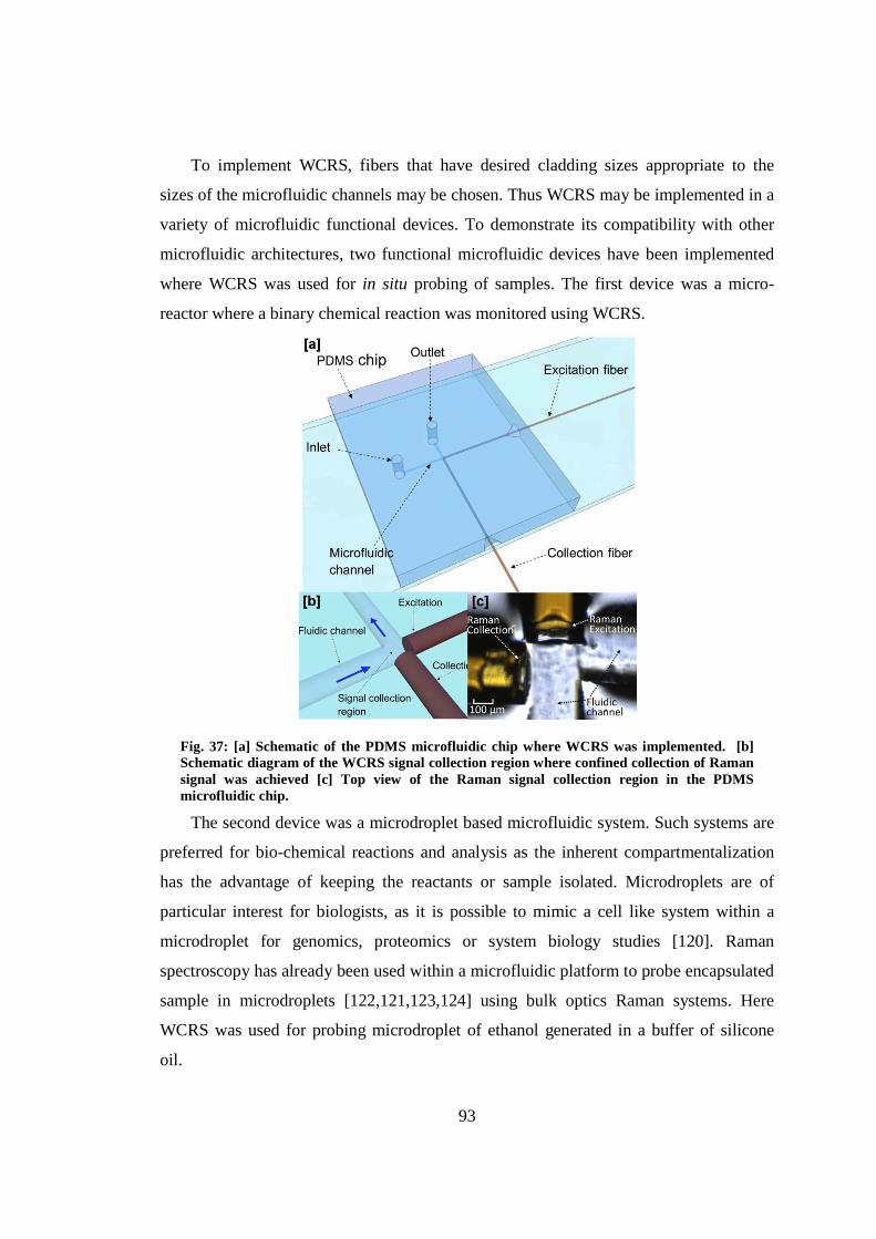
93
To implement WCRS, fibers that have desired cladding sizes appropriate to the
sizes of the microfluidic channels may be chosen. Thus WCRS may be implemented in a
variety of microfluidic functional devices. To demonstrate its compatibility with other
microfluidic architectures, two functional microfluidic devices have been implemented
where WCRS was used for in situ probing of samples. The first device was a micro-
reactor where a binary chemical reaction was monitored using WCRS.
Fig. 37: [a] Schematic of the PDMS microfluidic chip where WCRS was implemented. [b] Schematic diagram of the WCRS signal collection region where confined collection of Raman signal was achieved [c] Top view of the Raman signal collection region in the PDMS microfluidic chip.
The second device was a microdroplet based microfluidic system. Such systems are
preferred for bio-chemical reactions and analysis as the inherent compartmentalization
has the advantage of keeping the reactants or sample isolated. Microdroplets are of
particular interest for biologists, as it is possible to mimic a cell like system within a
microdroplet for genomics, proteomics or system biology studies [120]. Raman
spectroscopy has already been used within a microfluidic platform to probe encapsulated
sample in microdroplets [122,121,123,124] using bulk optics Raman systems. Here
WCRS was used for probing microdroplet of ethanol generated in a buffer of silicone
oil.
94
Fiber based Raman detection realized in microfluidics through WCRS is an
important step forward in the field of MRS; it enables rapid analyte detection with a
significantly reduced sample volume.
6.2 Embedding fiber into the microfluidic chip
The microfluidic chip was fabricated using soft lithography in PDMS [7]. To embed
optical fiber into the chip, fiber insertion channels were defined in the mold. The
fabrication procedure for a mold with pre-defined fiber insertion channels is explained in
detail in chapter 2. Fiber insertion channels were defined by placing pieces of fibers on
the silicon substrate and fixing it using UV curable adhesive (Norland). The size of the
fluidic channel near the detection region also depends on the total diameter of the optical
fiber. Commercially available multimode optical fibers have diameter range of 125 µm
to 250 µm. A negative photoresist (SU8, Microchem) was used to define other
microfluidic channels. To combine the channels defined by the fiber to the channel
defined by photoresist, the photoresist was spun on top of the silicon substrate to which
the fiber pieces were already attached. Using photolithography, SU8 channels were
defined on the substrate in such a way that the SU8 channel would be physically
connected to the fiber which is stuck on to the mold.
Once the mold was prepared, the PDMS chip was fabricated using soft lithography
and the excitation and collection fibers were inserted into the chip as shown in Fig. 37a.
Since the fiber insertion channel was predefined for the desired collection geometry, the
alignment requirement was minimal while inserting the fiber into the channel as shown
in Fig. 37b and Fig. 37c.
6.3 Raman detection system
The Raman signal was excited and collected using low OH multimode fibers. For all
the experiments discussed in this chapter, except those to study the effect of core size on
collection efficiency, a multimode fiber (Polymicro Technologies, Arizona, USA) with a
core size of 200 µm was used. A laser of wavelength 785 nm (Maximum power
~450mW) was used for Raman excitation. The laser was coupled into the optical fiber
through an SMA connector and the other end was embedded into the microfluidic chip.
95
The tip of the collection fiber, also embedded in the microfluidic chip, collected the
Raman signal which was then coupled to the spectrometer (Shamrock SR-303i, Andor
Technology) through a telescopic system to match the F-number of the fiber to that of
the spectrometer. A long-pass filter (cut off wavelength 795.2nm, Semrock, Inc. USA)
was incorporated between the two telescope lenses to filter out the Rayleigh scattered
photons. The spectrometer employed a 400 lines/mm grating and was equipped with a
deep depletion, back-illuminated and thermoelectrically cooled CCD camera (Newton,
Andor Technology). The resolution of the Raman system for a slit width of 150 µm, was
measured by the FWHM of the ethanol peak at 884 cm-1 and was found to be better than
14 cm-1.
6.4 Characterization of the device
WCRS is based on two concepts of confinement – confinement of the Raman signal
collection and confinement of the sample. To understand the requirement of the former,
consider that the output from the optical fiber diverges at an angle 12.70. For a length
<200 µm the beam size is comparable to the size of the core beyond which the power
density drops down significantly. Hence it is important to collect the Raman signal from
a region close to the apex of the excitation fiber, and the same logic applies to the
collection fiber for maximum collection efficiency. Fig. 38a shows that the maximum
overlap of excitation and collection is achieved by collecting the signal right at the apex
of the fiber.
The second confinement required is in terms of the sample. The microfluidic
channel, which has similar size as that of the excitation and collection waveguide, can
confine the sample within the confined signal collection region. One of the advantages
of this approach is that no other part of the microfluidic channel or substrate overlaps
with the collection volume; hence there would be no spurious background from the
substrate in the Raman spectra acquired using WCRS. Also, since the channel size is of
the order of 125 µm - 250µm, the required amount of sample volume is five orders of
magnitude lower than that of its probe based counterpart as shown in Fig. 38b. It is
important to note that a further reduction in channel size is possible if instead of optical
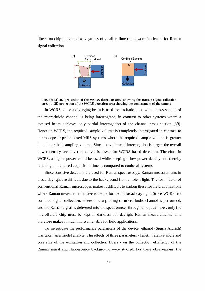
96
fibers, on-chip integrated waveguides of smaller dimensions were fabricated for Raman
signal collection.
Fig. 38: [a] 2D projection of the WCRS detection area, showing the Raman signal collection area [b] 2D projection of the WCRS detection area showing the confinement of the sample
In WCRS, since a diverging beam is used for excitation, the whole cross section of
the microfluidic channel is being interrogated, in contrast to other systems where a
focused beam achieves only partial interrogation of the channel cross section [89].
Hence in WCRS, the required sample volume is completely interrogated in contrast to
microscope or probe based MRS systems where the required sample volume is greater
than the probed sampling volume. Since the volume of interrogation is larger, the overall
power density seen by the analyte is lower for WCRS based detection. Therefore in
WCRS, a higher power could be used while keeping a low power density and thereby
reducing the required acquisition time as compared to confocal systems.
Since sensitive detectors are used for Raman spectroscopy, Raman measurements in
broad daylight are difficult due to the background from ambient light. The form factor of
conventional Raman microscopes makes it difficult to darken these for field applications
where Raman measurements have to be performed in broad day light. Since WCRS has
confined signal collection, where in-situ probing of microfluidic channel is performed,
and the Raman signal is delivered into the spectrometer through an optical fiber, only the
microfluidic chip must be kept in darkness for daylight Raman measurements. This
therefore makes it much more amenable for field applications.
To investigate the performance parameters of the device, ethanol (Sigma Aldrich)
was taken as a model analyte. The effects of three parameters - length, relative angle and
core size of the excitation and collection fibers - on the collection efficiency of the
Raman signal and fluorescence background were studied. For these observations, the
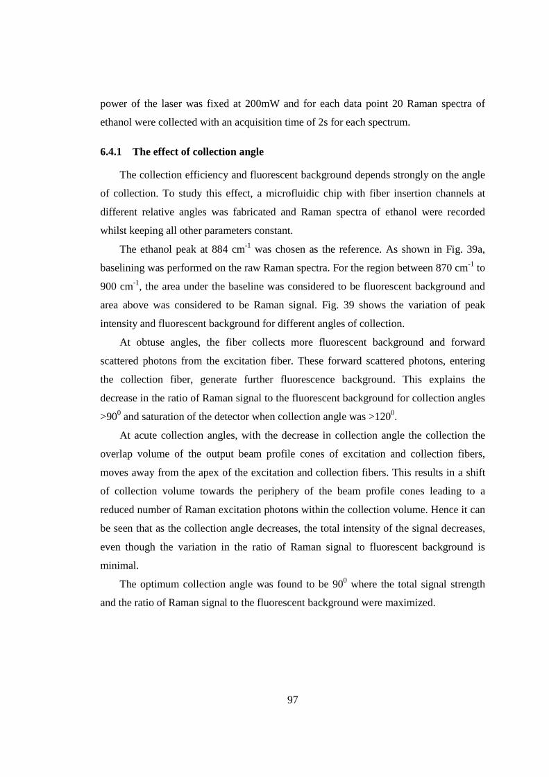
97
power of the laser was fixed at 200mW and for each data point 20 Raman spectra of
ethanol were collected with an acquisition time of 2s for each spectrum.
6.4.1 The effect of collection angle
The collection efficiency and fluorescent background depends strongly on the angle
of collection. To study this effect, a microfluidic chip with fiber insertion channels at
different relative angles was fabricated and Raman spectra of ethanol were recorded
whilst keeping all other parameters constant.
The ethanol peak at 884 cm-1 was chosen as the reference. As shown in Fig. 39a,
baselining was performed on the raw Raman spectra. For the region between 870 cm-1 to
900 cm-1, the area under the baseline was considered to be fluorescent background and
area above was considered to be Raman signal. Fig. 39 shows the variation of peak
intensity and fluorescent background for different angles of collection.
At obtuse angles, the fiber collects more fluorescent background and forward
scattered photons from the excitation fiber. These forward scattered photons, entering
the collection fiber, generate further fluorescence background. This explains the
decrease in the ratio of Raman signal to the fluorescent background for collection angles
>900 and saturation of the detector when collection angle was >1200.
At acute collection angles, with the decrease in collection angle the collection the
overlap volume of the output beam profile cones of excitation and collection fibers,
moves away from the apex of the excitation and collection fibers. This results in a shift
of collection volume towards the periphery of the beam profile cones leading to a
reduced number of Raman excitation photons within the collection volume. Hence it can
be seen that as the collection angle decreases, the total intensity of the signal decreases,
even though the variation in the ratio of Raman signal to fluorescent background is
minimal.
The optimum collection angle was found to be 900 where the total signal strength
and the ratio of Raman signal to the fluorescent background were maximized.
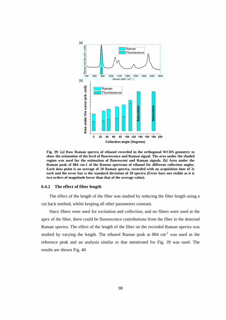
98
Fig. 39: [a] Raw Raman spectra of ethanol recorded in the orthogonal WCRS geometry to show the estimation of the level of fluorescence and Raman signal. The area under the shaded region was used for the estimation of fluorescent and Raman signals. [b] Area under the Raman peak of 884 cm-1 of the Raman spectrum of ethanol for different collection angles. Each data point is an average of 20 Raman spectra, recorded with an acquisition time of 2s each and the error bar is the standard deviation of 20 spectra (Error bars not visible as it is two orders of magnitude lower than that of the average value).
6.4.2 The effect of fiber length
The effect of the length of the fiber was studied by reducing the fiber length using a
cut back method, whilst keeping all other parameters constant.
Since fibers were used for excitation and collection, and no filters were used at the
apex of the fiber, there could be fluorescence contributions from the fiber in the detected
Raman spectra. The effect of the length of the fiber on the recorded Raman spectra was
studied by varying the length. The ethanol Raman peak at 884 cm-1 was used as the
reference peak and an analysis similar to that mentioned for Fig. 39 was used. The
results are shown Fig. 40.
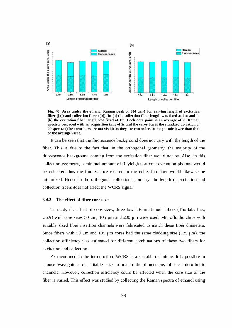
99
Fig. 40: Area under the ethanol Raman peak of 884 cm-1 for varying length of excitation fiber ([a]) and collection fiber ([b]). In [a] the collection fiber length was fixed at 1m and in [b] the excitation fiber length was fixed at 1m. Each data point is an average of 20 Raman spectra, recorded with an acquisition time of 2s and the error bar is the standard deviation of 20 spectra (The error bars are not visible as they are two orders of magnitude lower than that of the average value).
It can be seen that the fluorescence background does not vary with the length of the
fiber. This is due to the fact that, in the orthogonal geometry, the majority of the
fluorescence background coming from the excitation fiber would not be. Also, in this
collection geometry, a minimal amount of Rayleigh scattered excitation photons would
be collected thus the fluorescence excited in the collection fiber would likewise be
minimized. Hence in the orthogonal collection geometry, the length of excitation and
collection fibers does not affect the WCRS signal.
6.4.3 The effect of fiber core size
To study the effect of core sizes, three low OH multimode fibers (Thorlabs Inc.,
USA) with core sizes 50 µm, 105 µm and 200 µm were used. Microfluidic chips with
suitably sized fiber insertion channels were fabricated to match these fiber diameters.
Since fibers with 50 µm and 105 µm cores had the same cladding size (125 µm), the
collection efficiency was estimated for different combinations of these two fibers for
excitation and collection.
As mentioned in the introduction, WCRS is a scalable technique. It is possible to
choose waveguides of suitable size to match the dimensions of the microfluidic
channels. However, collection efficiency could be affected when the core size of the
fiber is varied. This effect was studied by collecting the Raman spectra of ethanol using
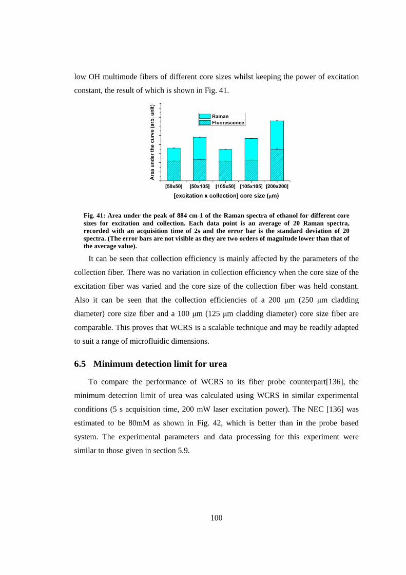
100
low OH multimode fibers of different core sizes whilst keeping the power of excitation
constant, the result of which is shown in Fig. 41.
Fig. 41: Area under the peak of 884 cm-1 of the Raman spectra of ethanol for different core sizes for excitation and collection. Each data point is an average of 20 Raman spectra, recorded with an acquisition time of 2s and the error bar is the standard deviation of 20 spectra. (The error bars are not visible as they are two orders of magnitude lower than that of the average value).
It can be seen that collection efficiency is mainly affected by the parameters of the
collection fiber. There was no variation in collection efficiency when the core size of the
excitation fiber was varied and the core size of the collection fiber was held constant.
Also it can be seen that the collection efficiencies of a 200 µm (250 µm cladding
diameter) core size fiber and a 100 µm (125 µm cladding diameter) core size fiber are
comparable. This proves that WCRS is a scalable technique and may be readily adapted
to suit a range of microfluidic dimensions.
6.5 Minimum detection limit for urea
To compare the performance of WCRS to its fiber probe counterpart[136], the
minimum detection limit of urea was calculated using WCRS in similar experimental
conditions (5 s acquisition time, 200 mW laser excitation power). The NEC [136] was
estimated to be 80mM as shown in Fig. 42, which is better than in the probe based
system. The experimental parameters and data processing for this experiment were
similar to those given in section 5.9.
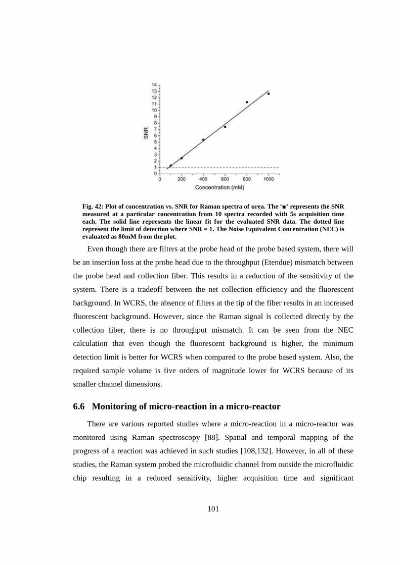
101
Fig. 42: Plot of concentration vs. SNR for Raman spectra of urea. The ‘’ represents the SNR measured at a particular concentration from 10 spectra recorded with 5s acquisition time each. The solid line represents the linear fit for the evaluated SNR data. The dotted line represent the limit of detection where SNR = 1. The Noise Equivalent Concentration (NEC) is evaluated as 80mM from the plot.
Even though there are filters at the probe head of the probe based system, there will
be an insertion loss at the probe head due to the throughput (Etendue) mismatch between
the probe head and collection fiber. This results in a reduction of the sensitivity of the
system. There is a tradeoff between the net collection efficiency and the fluorescent
background. In WCRS, the absence of filters at the tip of the fiber results in an increased
fluorescent background. However, since the Raman signal is collected directly by the
collection fiber, there is no throughput mismatch. It can be seen from the NEC
calculation that even though the fluorescent background is higher, the minimum
detection limit is better for WCRS when compared to the probe based system. Also, the
required sample volume is five orders of magnitude lower for WCRS because of its
smaller channel dimensions.
6.6 Monitoring of micro-reaction in a micro-reactor
There are various reported studies where a micro-reaction in a micro-reactor was
monitored using Raman spectroscopy [88]. Spatial and temporal mapping of the
progress of a reaction was achieved in such studies [108,132]. However, in all of these
studies, the Raman system probed the microfluidic channel from outside the microfluidic
chip resulting in a reduced sensitivity, higher acquisition time and significant
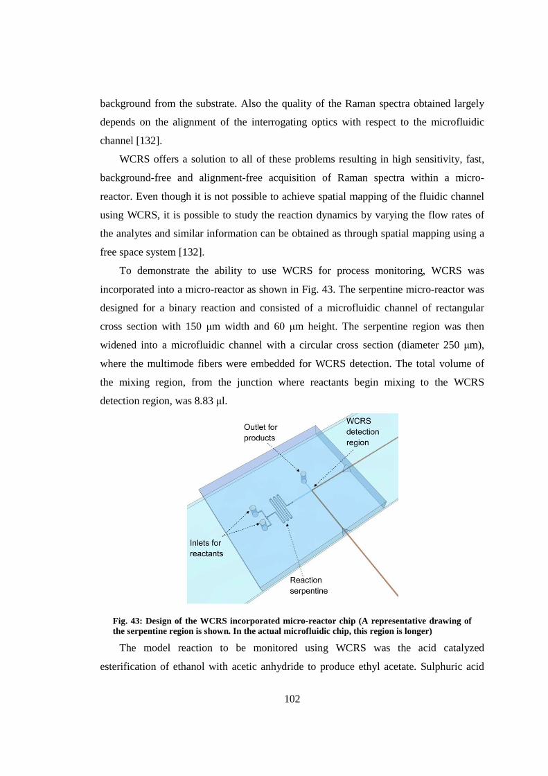
102
background from the substrate. Also the quality of the Raman spectra obtained largely
depends on the alignment of the interrogating optics with respect to the microfluidic
channel [132].
WCRS offers a solution to all of these problems resulting in high sensitivity, fast,
background-free and alignment-free acquisition of Raman spectra within a micro-
reactor. Even though it is not possible to achieve spatial mapping of the fluidic channel
using WCRS, it is possible to study the reaction dynamics by varying the flow rates of
the analytes and similar information can be obtained as through spatial mapping using a
free space system [132].
To demonstrate the ability to use WCRS for process monitoring, WCRS was
incorporated into a micro-reactor as shown in Fig. 43. The serpentine micro-reactor was
designed for a binary reaction and consisted of a microfluidic channel of rectangular
cross section with 150 µm width and 60 µm height. The serpentine region was then
widened into a microfluidic channel with a circular cross section (diameter 250 µm),
where the multimode fibers were embedded for WCRS detection. The total volume of
the mixing region, from the junction where reactants begin mixing to the WCRS
detection region, was 8.83 µl.
Fig. 43: Design of the WCRS incorporated micro-reactor chip (A representative drawing of the serpentine region is shown. In the actual microfluidic chip, this region is longer)
The model reaction to be monitored using WCRS was the acid catalyzed
esterification of ethanol with acetic anhydride to produce ethyl acetate. Sulphuric acid
103
was used as the catalyst for the reaction, a minute amount of which was added into the
reactants prior to the reaction. All the reagents used (Sigma Aldrich) were of analytical
quality. The reaction was carried out at room temperature ~ 22 0C. The solutions were
pumped into the micro-reactor using syringe pumps (Harvard Apparatus). The
stoichiometric ratio of acetic anhydride to ethanol was 1:2 for this reaction, which is
1:3.24 in volume. The ratio of the flow rates of the reactants was fixed at 1:4 since
ethanol was the carrier solvent.
The progress of reaction was studied at different interaction time scales for a binary
reaction. By changing the total flow speed, the interaction time for the two reactants was
varied. Interaction time was the time takes for the analyte to flow from the “T” junction,
where the analytes were combined, to the WCRS detection region. Prior to the actual
experiment the pure spectra of the reactants (acetic anhydride and ethanol) and product
(ethyl acetate) were obtained using WCRS and compared with the spectra of analyte for
an incomplete reaction as shown in Fig. 44a. Since the product analyte had an
incomplete reaction, the Raman peaks corresponding to all reactants and products could
be seen. The Raman spectra shown in Fig. 44a were smoothed using a Savitzky-Golay
smoothing filter and baselined using iterative modified polynomial fitting [141]. From
the spectra it is clear that the Raman peak at 671 cm-1 for acetic anhydride and the
Raman peak at 636 cm-1 for ethyl acetate would be the two representative peaks that
should be monitored to study the progress of the chemical reaction in the micro-reactor.
The concentration of ethanol was not monitored as it was the carrier solvent.
The total flow rate of the analyte was varied to change the interaction time of the
reactants. Raman spectra of the analyte were obtained using WCRS with an acquisition
time of 2s. Fig. 44b shows the variation in the concentration of ethyl acetate and acetic
anhydride with respect to the change in flow rate. Each data point is an average of 40
Raman spectra. Savitzky-Golay smoothing was performed on the Raman spectra as a
post processing step before estimating the peak intensity value. It was observed that, at
low flow rates, the reaction completed within the interaction time and the peaks
corresponding to acetic anhydride were missing from the recorded Raman spectra.
However for higher flow rates the reaction was incomplete and the acetic anhydride peak
was still visible in the Raman spectra and the intensity of the peak corresponding to ethyl
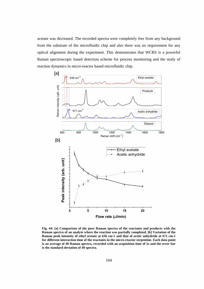
104
acetate was decreased. The recorded spectra were completely free from any background
from the substrate of the microfluidic chip and also there was no requirement for any
optical alignment during the experiment. This demonstrates that WCRS is a powerful
Raman spectroscopic based detection scheme for process monitoring and the study of
reaction dynamics in micro-reactor based microfluidic chip.
Fig. 44: [a] Comparison of the pure Raman spectra of the reactants and products with the Raman spectra of an analyte where the reaction was partially completed. [b] Variation of the Raman peak intensity of ethyl acetate at 636 cm-1 and that of acetic anhydride at 671 cm-1 for different interaction time of the reactants in the micro-reactor serpentine. Each data point is an average of 40 Raman spectra, recorded with an acquisition time of 2s and the error bar is the standard deviation of 40 spectra.
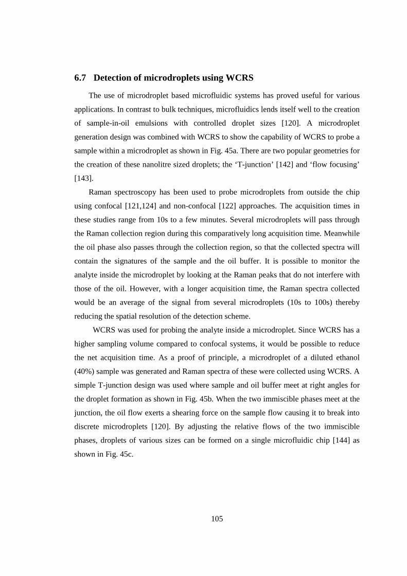
105
6.7 Detection of microdroplets using WCRS
The use of microdroplet based microfluidic systems has proved useful for various
applications. In contrast to bulk techniques, microfluidics lends itself well to the creation
of sample-in-oil emulsions with controlled droplet sizes [120]. A microdroplet
generation design was combined with WCRS to show the capability of WCRS to probe a
sample within a microdroplet as shown in Fig. 45a. There are two popular geometries for
the creation of these nanolitre sized droplets; the ‘T-junction’ [142] and ‘flow focusing’
[143].
Raman spectroscopy has been used to probe microdroplets from outside the chip
using confocal [121,124] and non-confocal [122] approaches. The acquisition times in
these studies range from 10s to a few minutes. Several microdroplets will pass through
the Raman collection region during this comparatively long acquisition time. Meanwhile
the oil phase also passes through the collection region, so that the collected spectra will
contain the signatures of the sample and the oil buffer. It is possible to monitor the
analyte inside the microdroplet by looking at the Raman peaks that do not interfere with
those of the oil. However, with a longer acquisition time, the Raman spectra collected
would be an average of the signal from several microdroplets (10s to 100s) thereby
reducing the spatial resolution of the detection scheme.
WCRS was used for probing the analyte inside a microdroplet. Since WCRS has a
higher sampling volume compared to confocal systems, it would be possible to reduce
the net acquisition time. As a proof of principle, a microdroplet of a diluted ethanol
(40%) sample was generated and Raman spectra of these were collected using WCRS. A
simple T-junction design was used where sample and oil buffer meet at right angles for
the droplet formation as shown in Fig. 45b. When the two immiscible phases meet at the
junction, the oil flow exerts a shearing force on the sample flow causing it to break into
discrete microdroplets [120]. By adjusting the relative flows of the two immiscible
phases, droplets of various sizes can be formed on a single microfluidic chip [144] as
shown in Fig. 45c.
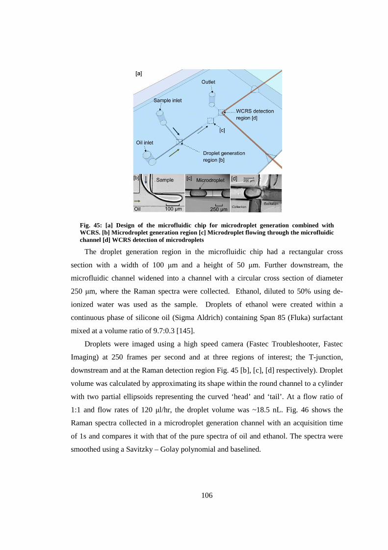
106
Fig. 45: [a] Design of the microfluidic chip for microdroplet generation combined with WCRS. [b] Microdroplet generation region [c] Microdroplet flowing through the microfluidic channel [d] WCRS detection of microdroplets
The droplet generation region in the microfluidic chip had a rectangular cross
section with a width of 100 µm and a height of 50 µm. Further downstream, the
microfluidic channel widened into a channel with a circular cross section of diameter
250 µm, where the Raman spectra were collected. Ethanol, diluted to 50% using de-
ionized water was used as the sample. Droplets of ethanol were created within a
continuous phase of silicone oil (Sigma Aldrich) containing Span 85 (Fluka) surfactant
mixed at a volume ratio of 9.7:0.3 [145].
Droplets were imaged using a high speed camera (Fastec Troubleshooter, Fastec
Imaging) at 250 frames per second and at three regions of interest; the T-junction,
downstream and at the Raman detection region Fig. 45 [b], [c], [d] respectively). Droplet
volume was calculated by approximating its shape within the round channel to a cylinder
with two partial ellipsoids representing the curved ‘head’ and ‘tail’. At a flow ratio of
1:1 and flow rates of 120 µl/hr, the droplet volume was ~18.5 nL. Fig. 46 shows the
Raman spectra collected in a microdroplet generation channel with an acquisition time
of 1s and compares it with that of the pure spectra of oil and ethanol. The spectra were
smoothed using a Savitzky – Golay polynomial and baselined.
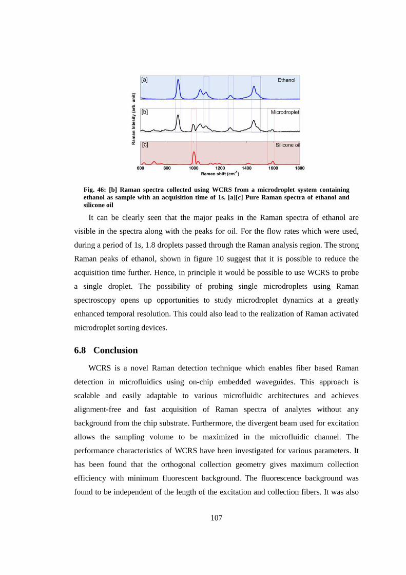
107
Fig. 46: [b] Raman spectra collected using WCRS from a microdroplet system containing ethanol as sample with an acquisition time of 1s. [a][c] Pure Raman spectra of ethanol and silicone oil
It can be clearly seen that the major peaks in the Raman spectra of ethanol are
visible in the spectra along with the peaks for oil. For the flow rates which were used,
during a period of 1s, 1.8 droplets passed through the Raman analysis region. The strong
Raman peaks of ethanol, shown in figure 10 suggest that it is possible to reduce the
acquisition time further. Hence, in principle it would be possible to use WCRS to probe
a single droplet. The possibility of probing single microdroplets using Raman
spectroscopy opens up opportunities to study microdroplet dynamics at a greatly
enhanced temporal resolution. This could also lead to the realization of Raman activated
microdroplet sorting devices.
6.8 Conclusion
WCRS is a novel Raman detection technique which enables fiber based Raman
detection in microfluidics using on-chip embedded waveguides. This approach is
scalable and easily adaptable to various microfluidic architectures and achieves
alignment-free and fast acquisition of Raman spectra of analytes without any
background from the chip substrate. Furthermore, the divergent beam used for excitation
allows the sampling volume to be maximized in the microfluidic channel. The
performance characteristics of WCRS have been investigated for various parameters. It
has been found that the orthogonal collection geometry gives maximum collection
efficiency with minimum fluorescent background. The fluorescence background was
found to be independent of the length of the excitation and collection fibers. It was also
108
shown that the collection efficiency is mainly dependent on the core size of the
collection fiber.
WCRS can be used for sensitive analyte detection with minimal sample preparation.
The minimum detection limit of this device to detect urea was estimated to be 80mM for
an acquisition time of 5s with 200mW excitation power which is better than its probe
based counterpart [136]. This would pave the way to developing sensitive and portable
bioanalyte detection devices using Raman spectroscopy that are suitable for detection
with minimal sample preparation requirements. Another important feature of WCRS is
that it could be easily combined with other microfluidic functionalities. As a proof of
principle, WCRS was implemented in two microfluidic applications. WCRS was used
for process monitoring in a micro-reactor and showed that the reaction dynamics could
be studied through Raman spectroscopy. WCRS was also used to probe microdroplets in
a microdroplet based microfluidic system. It was possible to obtain the Raman signature
of the sample in the microdroplet with a very low acquisition time which could lead to
development of Raman activated microdroplet sorting devices.
WCRS is a generic technique which is easily adaptable to various microfluidic
platforms and is a key the development towards efficient, alignment-free, portable MRS
devices for sensing and process monitoring that are suitable for field applications. With
WCRS, it is now possible to translate many MRS devices, implemented in bulk optics
geometries into a fiber based alignment-free geometry. It is possible to implement
variants of Raman spectroscopy such as SERS and resonance Raman spectroscopy, in
WCRS to extend its applicability. Further exploration is necessary for biological
applications of WCRS. Portable microfluidic devices with Raman spectroscopic
detection, realized through WCRS, may have applications in point of care disease
diagnosis, drug development, pharmaceutical manufacturing, cell biology, proteomics
and environmental sensing.
Relevant publications
• Ashok PC, Singh GP, Rendall HA, Krauss TF, Dholakia K (2011)
Waveguide confined raman spectroscopy for microfluidic interrogation. Lab
Chip 11 (7):1262 - 1270. doi:10.1039/c0lc00462f
109
• Ashok PC, Singh GP, Luca ACD, Mazilu M, Dholakia K (2010) Embedded
fiber probes for raman spectroscopic detection in microfluidics. Paper
presented at the Photonics 2010, Guwahati, India.
• Book Chapter: Ashok PC, Dholakia K (In press) Microfluidic raman
spectroscopy for bio-chemical sensing and analysis. In: Fritzsche W, Popp J
(eds) Springer series on chemical sensors and biosensors: Optical nano- and
microsystems for bioanalytics. Springer,
Patent
• Application: The University of St. Andrews Ashok PC, Singh GP, Dholakia
K, “Waveguide localized Raman spectroscopy”, UK patent application No.
GB1016270.9
Publicity
• Exhibited WCRS technology in 2011 Scottish Enterprise Technology
Showcase (June 2011, Glasgow) as one of the potential technology
opportunity from Scottish University Physics Alliance (SUPA).
Contribution
P. C. Ashok conceived, designed and implemented WCRS technique. P. C. Ashok
performed experiments. G. P. Singh assisted the work as a consultant on various aspects
of Raman spectroscopy. H. A. Rendall assisted in performing microdroplet experiments
and drawn the schematic diagrams of the fluidic chips, used for publication.
110
7. Enhanced bioanalyte detection in waveguide confined Raman spectroscopy using wavelength modulation
7.1 Introduction
In WCRS, as discussed in chapter 6, since fibers are used to excite and collect the
Raman signals, the recorded spectra contain fluorescence background from both the
fiber and the sample. This would effectively limit the detection sensitivity of this
technique as the background fluorescence shadows the weak Raman signals. Numerous
methods have been proposed to reduce or suppress the fluorescence background [146-
151]. A continuous wavelength modulation technique was employed that periodically
changes the excitation wavelength thereby distinguishing between the static background
and the modulated Raman peaks [140]. Additionally, the use of the continuous
wavelength modulation enhances the Raman Signal to Noise Ratio (SNR) as compared
to the standard shifted excitation Raman spectroscopic methods [152].
Wavelength modulation was implemented in WCRS to eliminate the fluorescent
background from the recorded Raman spectra. Urea solution was used as a model
analyte to estimate the performance characteristics of the device. The modulation
parameters were optimized to maximize the sensitivity. This sensitivity was then
compared to that of standard Raman detection.
7.2 Wavelength modulation implemented in a WCRS device
The schematic of the bioanalyte detection system is shown in Fig. 47a. A tunable
diode laser (Sacher, Littman configuration, maximum power 1 W and total tuning range
200 GHz) centred at 785 nm was coupled into a low OH multimode fiber (Polymicro
Technologies, Arizona, USA) of core diameter 200 µm which delivered the beam into
the microfluidic chip for excitation. Another fiber of the same specification was used to
collect the Raman signal from the microfluidic channel and couple it into a spectrometer
(Shamrock SR-303i, Andor Technology) through an F-number matcher. The
spectrometer was equipped with a 400 lines/mm grating with a deep depletion, back
illuminated and thermoelectrically cooled CCD camera (Newton, Andor Technology).
Both the excitation and collection fibers were embedded into the microfluidic channels.
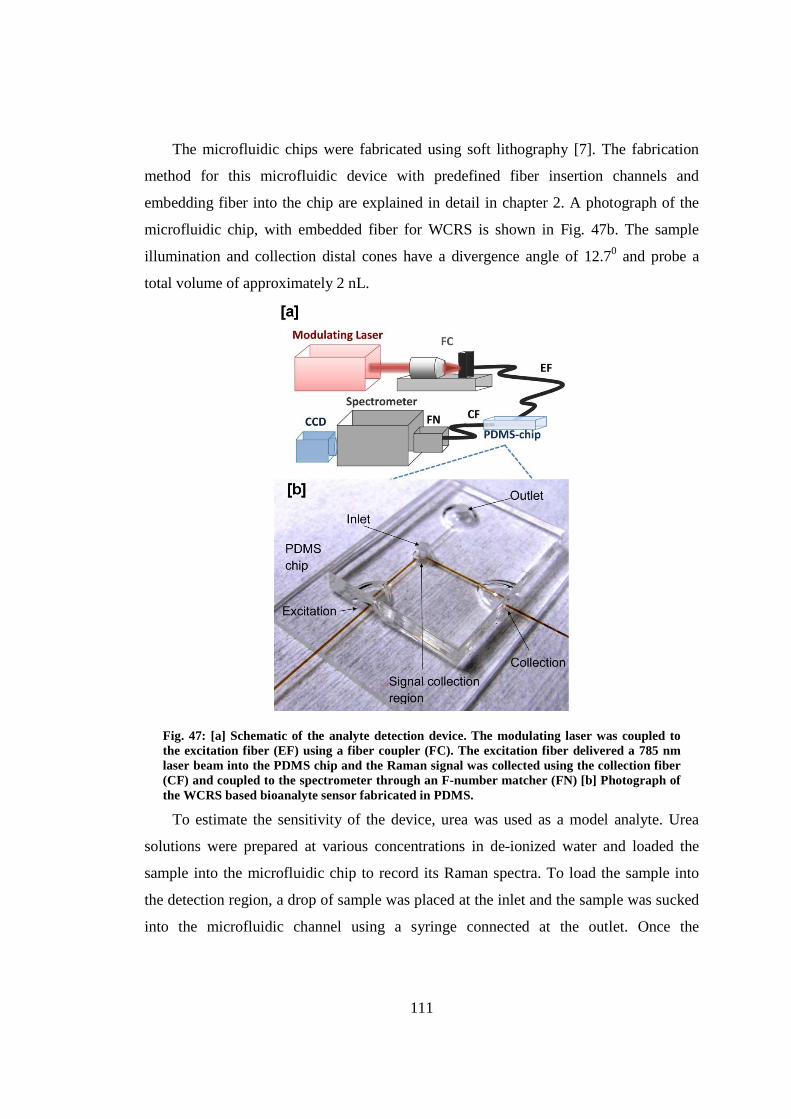
111
The microfluidic chips were fabricated using soft lithography [7]. The fabrication
method for this microfluidic device with predefined fiber insertion channels and
embedding fiber into the chip are explained in detail in chapter 2. A photograph of the
microfluidic chip, with embedded fiber for WCRS is shown in Fig. 47b. The sample
illumination and collection distal cones have a divergence angle of 12.70 and probe a
total volume of approximately 2 nL.
Fig. 47: [a] Schematic of the analyte detection device. The modulating laser was coupled to the excitation fiber (EF) using a fiber coupler (FC). The excitation fiber delivered a 785 nm laser beam into the PDMS chip and the Raman signal was collected using the collection fiber (CF) and coupled to the spectrometer through an F-number matcher (FN) [b] Photograph of the WCRS based bioanalyte sensor fabricated in PDMS.
To estimate the sensitivity of the device, urea was used as a model analyte. Urea
solutions were prepared at various concentrations in de-ionized water and loaded the
sample into the microfluidic chip to record its Raman spectra. To load the sample into
the detection region, a drop of sample was placed at the inlet and the sample was sucked
into the microfluidic channel using a syringe connected at the outlet. Once the
112
measurement was complete, the channel was rinsed with de-ionized water to avoid
contamination.
7.3 Raman acquisition method
The principle behind wavelength modulated Raman spectroscopy is the fact that,
unlike the fluorescent background, Raman signals shift continuously with modulation of
the excitation wavelength [140]. By selecting only the modulated component of the
acquired signals, the fluorescence background is completely filtered out.
The experiment consists of acquiring many short-duration spectra (single
acquisition time ~ 4s) each corresponding to a different excitation wavelength while the
laser wavelength is sinusoidally modulated (modulation frequency 45 mHz, amplitude
∆ν = 40 GHz). The total acquisition time is ~100s.
The SNR of the modulated Raman spectra depends on the modulation frequency,
amplitude and on the acquisition time. The optimum values for these parameters vary
depending on the detection geometry, fluorescence characteristics of the sample and
shape of the Raman bands. These parameters were experimentally optimized with
respect to the detection of the specific urea Raman peak considered [140].
Each set of the acquired spectra was normalized with respect to the laser intensity
and Principle Component Analysis (PCA) were used to obtain modulated Raman spectra
free from any fluorescence background contribution [152]. The first Principal
Component (PC) evaluated corresponds to the maximal variation between the spectra.
This variation is induced by the continuous shifts of the Raman peaks and gives the
derivative-like Raman spectrum where the fluorescence is eliminated. For each
measured dataset the standard Raman spectrum was obtained by averaging all the
modulated spectra belonging to that set.
7.4 Detection sensitivity
The strongest band of urea at 1010 cm-1, corresponding to the CN symmetric
stretching vibration band, was used to monitor the concentration of urea in the solution.
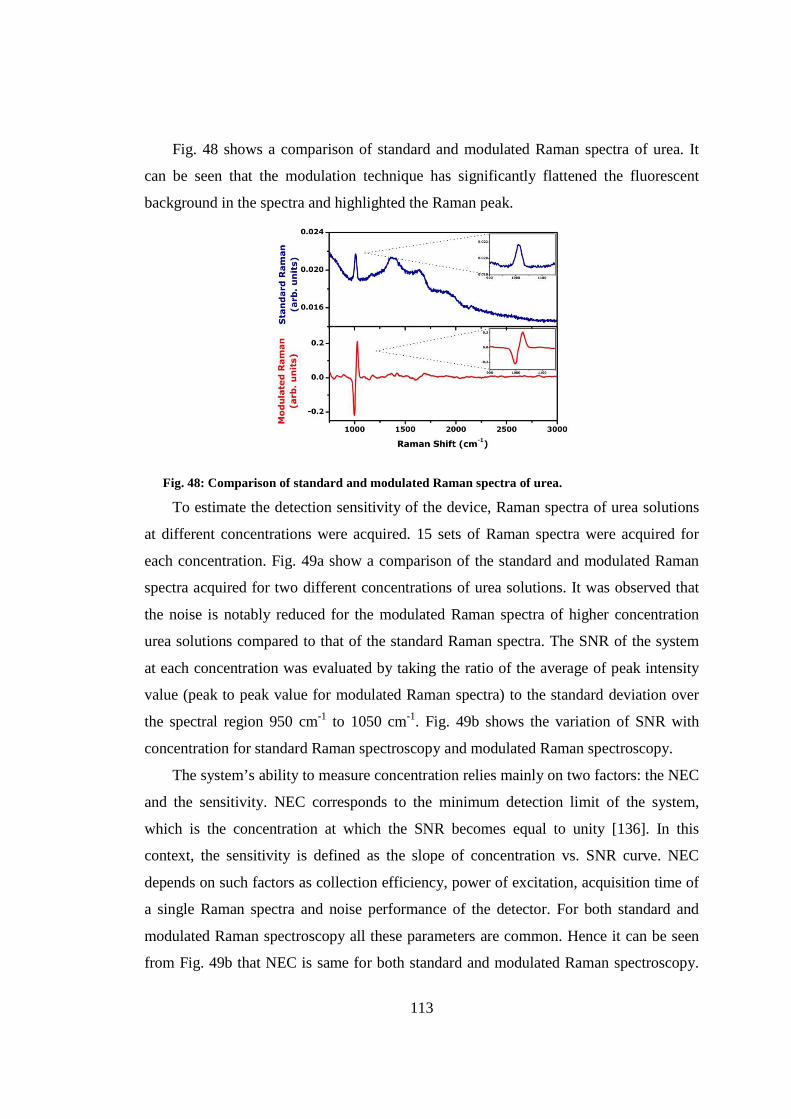
113
Fig. 48 shows a comparison of standard and modulated Raman spectra of urea. It
can be seen that the modulation technique has significantly flattened the fluorescent
background in the spectra and highlighted the Raman peak.
Fig. 48: Comparison of standard and modulated Raman spectra of urea.
To estimate the detection sensitivity of the device, Raman spectra of urea solutions
at different concentrations were acquired. 15 sets of Raman spectra were acquired for
each concentration. Fig. 49a show a comparison of the standard and modulated Raman
spectra acquired for two different concentrations of urea solutions. It was observed that
the noise is notably reduced for the modulated Raman spectra of higher concentration
urea solutions compared to that of the standard Raman spectra. The SNR of the system
at each concentration was evaluated by taking the ratio of the average of peak intensity
value (peak to peak value for modulated Raman spectra) to the standard deviation over
the spectral region 950 cm-1 to 1050 cm-1. Fig. 49b shows the variation of SNR with
concentration for standard Raman spectroscopy and modulated Raman spectroscopy.
The system’s ability to measure concentration relies mainly on two factors: the NEC
and the sensitivity. NEC corresponds to the minimum detection limit of the system,
which is the concentration at which the SNR becomes equal to unity [136]. In this
context, the sensitivity is defined as the slope of concentration vs. SNR curve. NEC
depends on such factors as collection efficiency, power of excitation, acquisition time of
a single Raman spectra and noise performance of the detector. For both standard and
modulated Raman spectroscopy all these parameters are common. Hence it can be seen
from Fig. 49b that NEC is same for both standard and modulated Raman spectroscopy.
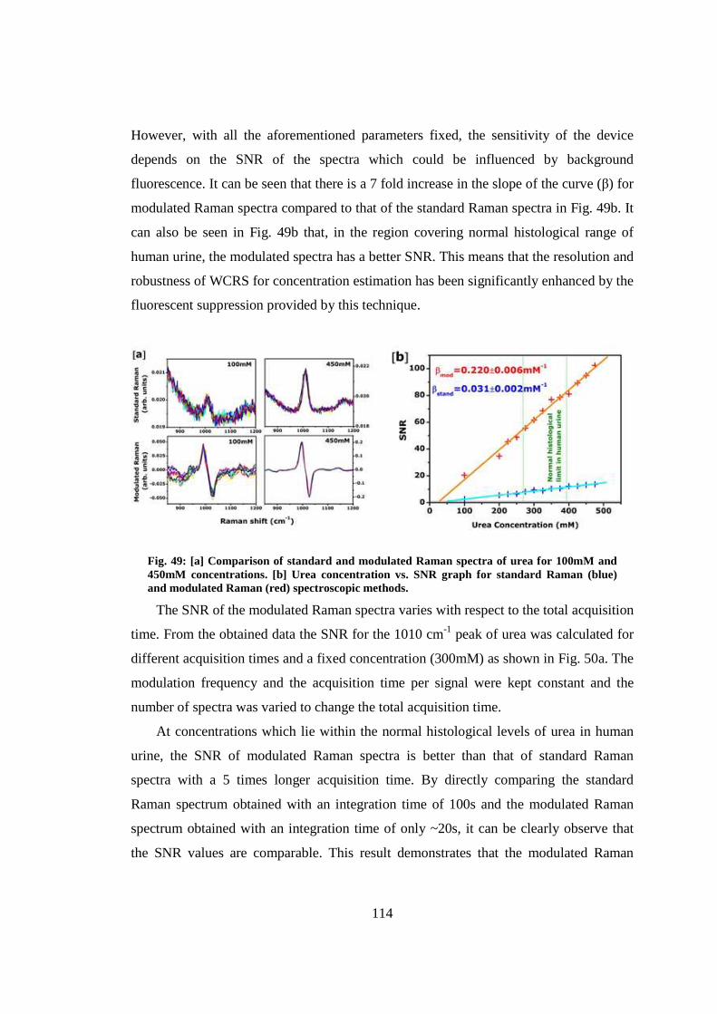
114
However, with all the aforementioned parameters fixed, the sensitivity of the device
depends on the SNR of the spectra which could be influenced by background
fluorescence. It can be seen that there is a 7 fold increase in the slope of the curve (β) for
modulated Raman spectra compared to that of the standard Raman spectra in Fig. 49b. It
can also be seen in Fig. 49b that, in the region covering normal histological range of
human urine, the modulated spectra has a better SNR. This means that the resolution and
robustness of WCRS for concentration estimation has been significantly enhanced by the
fluorescent suppression provided by this technique.
Fig. 49: [a] Comparison of standard and modulated Raman spectra of urea for 100mM and 450mM concentrations. [b] Urea concentration vs. SNR graph for standard Raman (blue) and modulated Raman (red) spectroscopic methods.
The SNR of the modulated Raman spectra varies with respect to the total acquisition
time. From the obtained data the SNR for the 1010 cm-1 peak of urea was calculated for
different acquisition times and a fixed concentration (300mM) as shown in Fig. 50a. The
modulation frequency and the acquisition time per signal were kept constant and the
number of spectra was varied to change the total acquisition time.
At concentrations which lie within the normal histological levels of urea in human
urine, the SNR of modulated Raman spectra is better than that of standard Raman
spectra with a 5 times longer acquisition time. By directly comparing the standard
Raman spectrum obtained with an integration time of 100s and the modulated Raman
spectrum obtained with an integration time of only ~20s, it can be clearly observe that
the SNR values are comparable. This result demonstrates that the modulated Raman
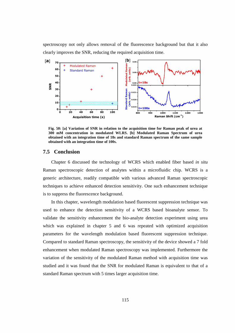
115
spectroscopy not only allows removal of the fluorescence background but that it also
clearly improves the SNR, reducing the required acquisition time.
Fig. 50: [a] Variation of SNR in relation to the acquisition time for Raman peak of urea at 300 mM concentration in modulated WLRS. [b] Modulated Raman Spectrum of urea obtained with an integration time of 18s and standard Raman spectrum of the same sample obtained with an integration time of 100s.
7.5 Conclusion
Chapter 6 discussed the technology of WCRS which enabled fiber based in situ
Raman spectroscopic detection of analytes within a microfluidic chip. WCRS is a
generic architecture, readily compatible with various advanced Raman spectroscopic
techniques to achieve enhanced detection sensitivity. One such enhancement technique
is to suppress the fluorescence background.
In this chapter, wavelength modulation based fluorescent suppression technique was
used to enhance the detection sensitivity of a WCRS based bioanalyte sensor. To
validate the sensitivity enhancement the bio-analyte detection experiment using urea
which was explained in chapter 5 and 6 was repeated with optimized acquisition
parameters for the wavelength modulation based fluorescent suppression technique.
Compared to standard Raman spectroscopy, the sensitivity of the device showed a 7 fold
enhancement when modulated Raman spectroscopy was implemented. Furthermore the
variation of the sensitivity of the modulated Raman method with acquisition time was
studied and it was found that the SNR for modulated Raman is equivalent to that of a
standard Raman spectrum with 5 times larger acquisition time.
116
Wavelength modulation based Raman spectroscopy has proved to be useful in
enhancing the bioanalyte detection sensitivity. However, the total acquisition time
required would be higher when implementing wavelength modulation technique since a
set of multiple spectra is required. It is also essential that the SNR of the Raman peaks in
each single spectrum acquisition should be greater than 1. Hence, as can be seen from
Fig. 49b, wavelength modulation based fluorescence suppression technique will not
improve the minimum detection limit. However this technique is capable of enhancing
the SNR of a Raman peak when the SNR is greater than 1 which is especially useful
when multicomponent detection is required from analyte which has relatively strong
fluorescence.
In this study the flexibility and compatibility of WCRS with advanced Raman
spectroscopic techniques in WCRS was demonstrated. The combination of WCRS with
fluorescent suppression techniques opens up opportunities to develop portable
microfluidic devices for a wide variety of analyte sensing applications. It may be
possible to implement other advanced techniques like SERS or Resonance Raman
spectroscopy in conjunction with WCRS to achieve further enhanced detection for
specific applications.
Relevant publications
• Ashok PC, Luca ACD, Mazilu M, Dholakia K (2011) Enhanced bioanalyte
detection in waveguide confined raman spectroscopy using modulation
techniques. J Biophot. doi:10.1002/jbio.201000107
Contributions
P. C. Ashok setup the optics and performed the experiment. A. C. De Luca
processed the acquired Raman spectra. M. Mazilu assisted in data processing.
117
8. Near infrared spectroscopic analysis of single malt scotch whisky in an optofluidic chip
8.1 Introduction
Quality standardization is an essential task in the liquor production industry. There
have been several techniques used for standardization based on the various physical and
chemical properties of alcoholic beverages. In the case of Scotch whisky the major
parameters that have been used for assessing quality are alcohol content, color
consistency and congener profile. Congeners are the organic compounds that are formed
during fermentation and amount to less than 1% of the total volume. However it is the
congener profile that dictates the flavor of the whisky [153].
Several optical detection techniques have been reported in the last two decades for
analyzing the quality of alcoholic beverages, particularly for analyzing Scotch whisky.
Ethanol content is one of the main parameters that determines quality. In authentic
whisky, the concentration of ethanol must be more than 40% of the volume.
Spectroscopic calibration of ethanol concentration in alcoholic beverages has been
previously achieved using a fiber optic probe [154]. Other laboratory based analytical
techniques have been proposed which utilize infrared (IR) spectroscopy to determine
ethanol content [155-159]. Ethanol concentration has also been measured using a non-
optical technique which determines the density of samples through a flow injection-
pervaporation method [160]. However distillation is required to implement this
technique which makes it time consuming compared to optical methods. Another
approach used mass spectroscopy to authenticate whisky samples [161,162]. In contrast
to the laboratory based analytical studies mentioned previously there have been attempts
to implement portable analytical devices. One of these was a handheld UV-vis-IR
spectrometer combined with a flow cell for Scotch whisky authentication [163]. A
separate study compared Near Infrared (NIR) fluorescence spectroscopy with NIR
Raman. In this study it was observed that Raman spectroscopy performed better for
concentration calibration, although the same paper raised concerns about implementing
laser based Raman spectroscopic detection in a production line using free-space Raman
detection devices [164]. Recently the same group reported an analytical technique to
118
detect counterfeit whisky samples using attenuated total reflectance with a diamond-
tipped immersion probe for mid-IR spectroscopy [153].
All of this literature and research demonstrates that spectroscopic techniques, when
combined with multivariate analysis, form a powerful tool to authenticate whisky
samples (or indeed other alcoholic beverages). However, the majority of these are
laboratory based techniques which require significant sample preparation
[153,157,162,161]. Also, the typical acquisition times needed ranges from 10s of
seconds to several minutes and sample volumes in the range of milli-liters. A solution to
these limitations would be to move this analytic technique into an optofluidic platform.
The field of optofluidics, which has emerged from the marriage of microfluidics with
photonics technologies, enables faster chemical analysis with reduced sample volumes in
miniaturized portable devices [14,165].
In this chapter, the use of a fiber based optofluidic chip for NIR spectroscopic
analysis of Scotch whisky is demonstrated. The very same device was recently shown to
yield what was termed Waveguide Confined Raman Spectroscopy (WCRS) within an
optofluidic chip. This offered alignment-free Raman spectroscopic detection of analytes
with very low sample volumes (in the order of few microliters) accompanied with
relatively short acquisition times (1-2 seconds) [166,167,136]. WCRS microfluidic chips
can be considered as microfluidic analogues to fiber optic Raman probes [93,96]. This
makes this optofluidic device compatible for use within a portable NIR Raman system.
This chip may not only record Raman spectra of the sample but naturally picks up
fluorescence present as well. This fluorescent component may be removed using
modulation methods for example [167]. However in this study Raman and fluorescent
properties of the sample are exploited. The optofluidic chip presented here was
fabricated in polydimethylsiloxane (PDMS) using soft lithography and does not require
any micro- optical filters. This makes the manufacturing cost of this chip up two orders
of magnitude less than that of a typical fiber based Raman probe. Although the low
manufacturing cost makes this chip suitable as a disposable one, it is possible to reuse
the chip by following a simple rinsing procedure with water between loading each
sample. Orthogonal collection geometry was employed in the WCRS chip to ensure
maximum collection of Raman photons, discarding the majority of the forward scattered
119
Rayleigh photons. It was possible to perform analysis of various whiskies with just 20
µl of sample without any special sample preparation. This is shown in Fig. 51. A
standard fiber Raman probe based detection would not readily allow analyte detection
with such low sample volumes. Also, since the sample to be detected is confined within
the microfluidic channel, any variation due to ethanol evaporation was avoided.
As a proof of principle to demonstrate the usefulness of this optofluidic device for
analyzing alcoholic beverages, different brands of Scotch whiskies available on the
market were analyzed. Raman spectra of these whisky samples were obtained and
various multivariate techniques were used to achieve both ethanol concentration
measurement and classifications of the different types of Scotch whisky tested. Partial
Least Square (PLS) calibration was performed to obtain the ethanol concentration and,
principal component analysis (PCA) was used to classify various brands based on flavor,
age and type of cask.
8.2 Experimental
The microfluidic chip was fabricated in PDMS using soft-lithography with pre-
defined fiber insertion channels as detailed in [166]. Two ultra-low OH multimode
optical fibers with core sizes of 200 µm (Polymicro Technologies) were embedded into
the chip for the excitation and collection of Raman signals. The fused silica in ultra-low-
OH fibers contain lesser hydroxyl component resulting in reduced fluorescence excited
in the fiber.
The procedure for acquiring Raman spectra of each sample is detailed in Fig. 52.
Whisky samples were directly loaded into the microfluidic chip without any special
preparation; 20 µl of whisky was placed at the sample inlet of microfluidic chip using a
micropipette. This drop of sample was then sucked into the microfluidic channel using a
1 ml syringe attached to the outlet of the microfluidic chip. Once the sample was sucked
into the signal detection region, Raman spectra of the sample was recorded with a 2 s
acquisition time. After Raman acquisition, any remaining liquid at the sample inlet was
wiped off and 40 µl of deionized water was passed into the microfluidic channel to rinse
the system. This rinsing procedure was sufficient to avoid any cross contamination
between samples. With a 2s acquisition time, the total time required to acquire a Raman
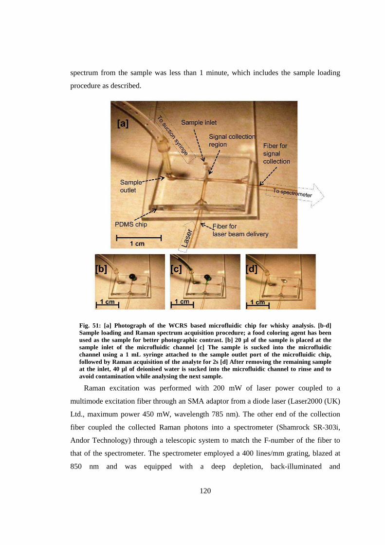
120
spectrum from the sample was less than 1 minute, which includes the sample loading
procedure as described.
Fig. 51: [a] Photograph of the WCRS based microfluidic chip for whisky analysis. [b-d] Sample loading and Raman spectrum acquisition procedure; a food coloring agent has been used as the sample for better photographic contrast. [b] 20 µl of the sample is placed at the sample inlet of the microfluidic channel [c] The sample is sucked into the microfluidic channel using a 1 mL syringe attached to the sample outlet port of the microfluidic chip, followed by Raman acquisition of the analyte for 2s [d] After removing the remaining sample at the inlet, 40 µl of deionised water is sucked into the microfluidic channel to rinse and to avoid contamination while analysing the next sample.
Raman excitation was performed with 200 mW of laser power coupled to a
multimode excitation fiber through an SMA adaptor from a diode laser (Laser2000 (UK)
Ltd., maximum power 450 mW, wavelength 785 nm). The other end of the collection
fiber coupled the collected Raman photons into a spectrometer (Shamrock SR-303i,
Andor Technology) through a telescopic system to match the F-number of the fiber to
that of the spectrometer. The spectrometer employed a 400 lines/mm grating, blazed at
850 nm and was equipped with a deep depletion, back-illuminated and
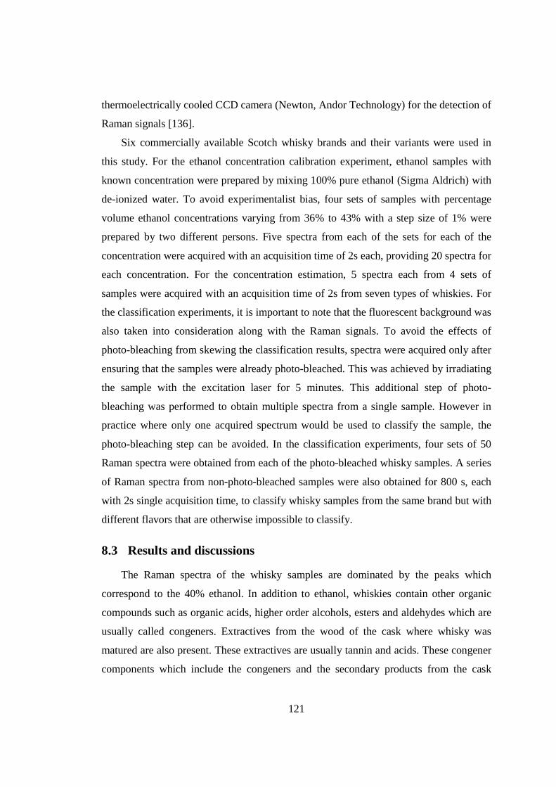
121
thermoelectrically cooled CCD camera (Newton, Andor Technology) for the detection of
Raman signals [136].
Six commercially available Scotch whisky brands and their variants were used in
this study. For the ethanol concentration calibration experiment, ethanol samples with
known concentration were prepared by mixing 100% pure ethanol (Sigma Aldrich) with
de-ionized water. To avoid experimentalist bias, four sets of samples with percentage
volume ethanol concentrations varying from 36% to 43% with a step size of 1% were
prepared by two different persons. Five spectra from each of the sets for each of the
concentration were acquired with an acquisition time of 2s each, providing 20 spectra for
each concentration. For the concentration estimation, 5 spectra each from 4 sets of
samples were acquired with an acquisition time of 2s from seven types of whiskies. For
the classification experiments, it is important to note that the fluorescent background was
also taken into consideration along with the Raman signals. To avoid the effects of
photo-bleaching from skewing the classification results, spectra were acquired only after
ensuring that the samples were already photo-bleached. This was achieved by irradiating
the sample with the excitation laser for 5 minutes. This additional step of photo-
bleaching was performed to obtain multiple spectra from a single sample. However in
practice where only one acquired spectrum would be used to classify the sample, the
photo-bleaching step can be avoided. In the classification experiments, four sets of 50
Raman spectra were obtained from each of the photo-bleached whisky samples. A series
of Raman spectra from non-photo-bleached samples were also obtained for 800 s, each
with 2s single acquisition time, to classify whisky samples from the same brand but with
different flavors that are otherwise impossible to classify.
8.3 Results and discussions
The Raman spectra of the whisky samples are dominated by the peaks which
correspond to the 40% ethanol. In addition to ethanol, whiskies contain other organic
compounds such as organic acids, higher order alcohols, esters and aldehydes which are
usually called congeners. Extractives from the wood of the cask where whisky was
matured are also present. These extractives are usually tannin and acids. These congener
components which include the congeners and the secondary products from the cask
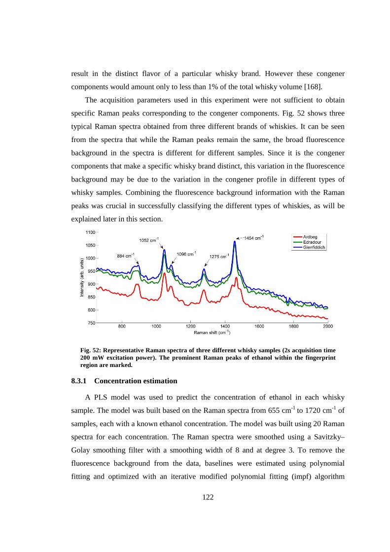
122
result in the distinct flavor of a particular whisky brand. However these congener
components would amount only to less than 1% of the total whisky volume [168].
The acquisition parameters used in this experiment were not sufficient to obtain
specific Raman peaks corresponding to the congener components. Fig. 52 shows three
typical Raman spectra obtained from three different brands of whiskies. It can be seen
from the spectra that while the Raman peaks remain the same, the broad fluorescence
background in the spectra is different for different samples. Since it is the congener
components that make a specific whisky brand distinct, this variation in the fluorescence
background may be due to the variation in the congener profile in different types of
whisky samples. Combining the fluorescence background information with the Raman
peaks was crucial in successfully classifying the different types of whiskies, as will be
explained later in this section.
Fig. 52: Representative Raman spectra of three different whisky samples (2s acquisition time 200 mW excitation power). The prominent Raman peaks of ethanol within the fingerprint region are marked.
8.3.1 Concentration estimation
A PLS model was used to predict the concentration of ethanol in each whisky
sample. The model was built based on the Raman spectra from 655 cm-1 to 1720 cm-1 of
samples, each with a known ethanol concentration. The model was built using 20 Raman
spectra for each concentration. The Raman spectra were smoothed using a Savitzky–
Golay smoothing filter with a smoothing width of 8 and at degree 3. To remove the
fluorescence background from the data, baselines were estimated using polynomial
fitting and optimized with an iterative modified polynomial fitting (impf) algorithm
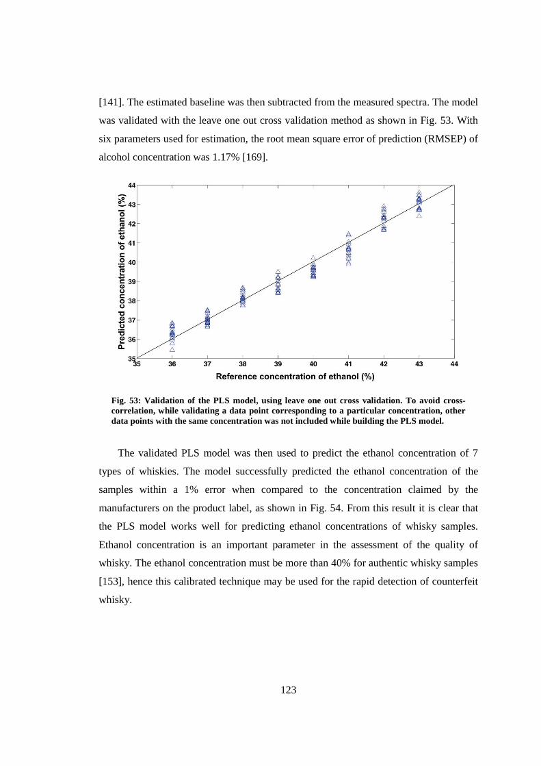
123
[141]. The estimated baseline was then subtracted from the measured spectra. The model
was validated with the leave one out cross validation method as shown in Fig. 53. With
six parameters used for estimation, the root mean square error of prediction (RMSEP) of
alcohol concentration was 1.17% [169].
Fig. 53: Validation of the PLS model, using leave one out cross validation. To avoid cross-correlation, while validating a data point corresponding to a particular concentration, other data points with the same concentration was not included while building the PLS model.
The validated PLS model was then used to predict the ethanol concentration of 7
types of whiskies. The model successfully predicted the ethanol concentration of the
samples within a 1% error when compared to the concentration claimed by the
manufacturers on the product label, as shown in Fig. 54. From this result it is clear that
the PLS model works well for predicting ethanol concentrations of whisky samples.
Ethanol concentration is an important parameter in the assessment of the quality of
whisky. The ethanol concentration must be more than 40% for authentic whisky samples
[153], hence this calibrated technique may be used for the rapid detection of counterfeit
whisky.
124
Fig. 54: Estimation of ethanol concentration in various whisky brands using a PLS model. The error bar gives the standard deviation of predicted concentration for 20 Raman spectra acquired from the same whisky type.
8.3.2 Classification of whisky samples
As discussed previously, although the acquired Raman spectra of whisky contain
only the Raman peaks that correspond to ethanol, the fluorescent background was
markedly different for different types of whisky. This difference may result from the
varying contributions of the congener components that are responsible for the color of
the whisky. For the ethanol concentration estimation, the fluorescence background was
discarded by performing a baseline subtraction on the data. However, the fluorescence
background proved very useful for categorizing different types of whisky. Hence for the
classification of the whisky samples PCA was performed on the acquired NIR spectra
just after the Savitzky-Golay smoothing with a smoothing width of 8 and degree of
smoothing 3. PCA is a multivariate technique which can be used for dimensionality
reduction. In the case of analyzing and classifying spectra, each pixel in the obtained
spectra can be considered as each parameter, which may or may not be correlated to
each other. PCA transforms this multidimensional space into a set of orthogonal co-
ordinates (principal components) in such a way that the first principal component would
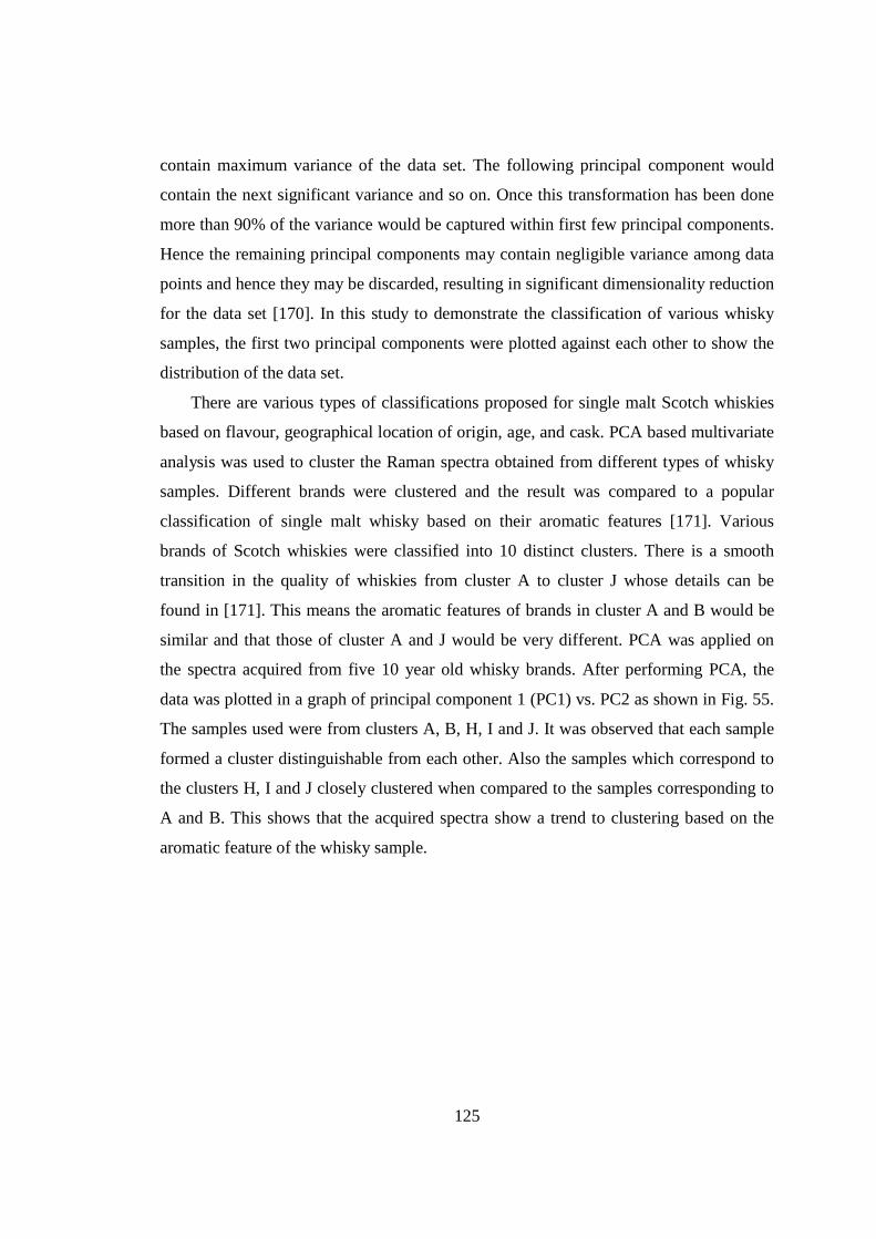
125
contain maximum variance of the data set. The following principal component would
contain the next significant variance and so on. Once this transformation has been done
more than 90% of the variance would be captured within first few principal components.
Hence the remaining principal components may contain negligible variance among data
points and hence they may be discarded, resulting in significant dimensionality reduction
for the data set [170]. In this study to demonstrate the classification of various whisky
samples, the first two principal components were plotted against each other to show the
distribution of the data set.
There are various types of classifications proposed for single malt Scotch whiskies
based on flavour, geographical location of origin, age, and cask. PCA based multivariate
analysis was used to cluster the Raman spectra obtained from different types of whisky
samples. Different brands were clustered and the result was compared to a popular
classification of single malt whisky based on their aromatic features [171]. Various
brands of Scotch whiskies were classified into 10 distinct clusters. There is a smooth
transition in the quality of whiskies from cluster A to cluster J whose details can be
found in [171]. This means the aromatic features of brands in cluster A and B would be
similar and that those of cluster A and J would be very different. PCA was applied on
the spectra acquired from five 10 year old whisky brands. After performing PCA, the
data was plotted in a graph of principal component 1 (PC1) vs. PC2 as shown in Fig. 55.
The samples used were from clusters A, B, H, I and J. It was observed that each sample
formed a cluster distinguishable from each other. Also the samples which correspond to
the clusters H, I and J closely clustered when compared to the samples corresponding to
A and B. This shows that the acquired spectra show a trend to clustering based on the
aromatic feature of the whisky sample.
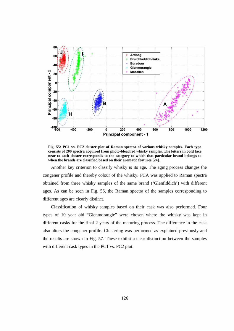
126
Fig. 55: PC1 vs. PC2 cluster plot of Raman spectra of various whisky samples. Each type consists of 200 spectra acquired from photo-bleached whisky samples. The letters in bold face near to each cluster corresponds to the category to which that particular brand belongs to when the brands are classified based on their aromatic features [24].
Another key criterion to classify whisky is its age. The aging process changes the
congener profile and thereby colour of the whisky. PCA was applied to Raman spectra
obtained from three whisky samples of the same brand (‘Glenfiddich’) with different
ages. As can be seen in Fig. 56, the Raman spectra of the samples corresponding to
different ages are clearly distinct.
Classification of whisky samples based on their cask was also performed. Four
types of 10 year old “Glenmorangie” were chosen where the whisky was kept in
different casks for the final 2 years of the maturing process. The difference in the cask
also alters the congener profile. Clustering was performed as explained previously and
the results are shown in Fig. 57. These exhibit a clear distinction between the samples
with different cask types in the PC1 vs. PC2 plot.
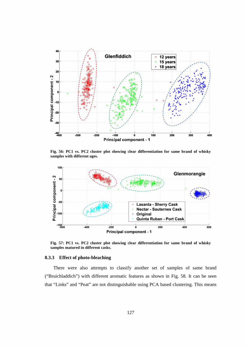
127
Fig. 56: PC1 vs. PC2 cluster plot showing clear differentiation for same brand of whisky samples with different ages.
Fig. 57: PC1 vs. PC2 cluster plot showing clear differentiation for same brand of whisky samples matured in different casks.
8.3.3 Effect of photo-bleaching
There were also attempts to classify another set of samples of same brand
(“Bruichladdich”) with different aromatic features as shown in Fig. 58. It can be seen
that “Links” and “Peat” are not distinguishable using PCA based clustering. This means
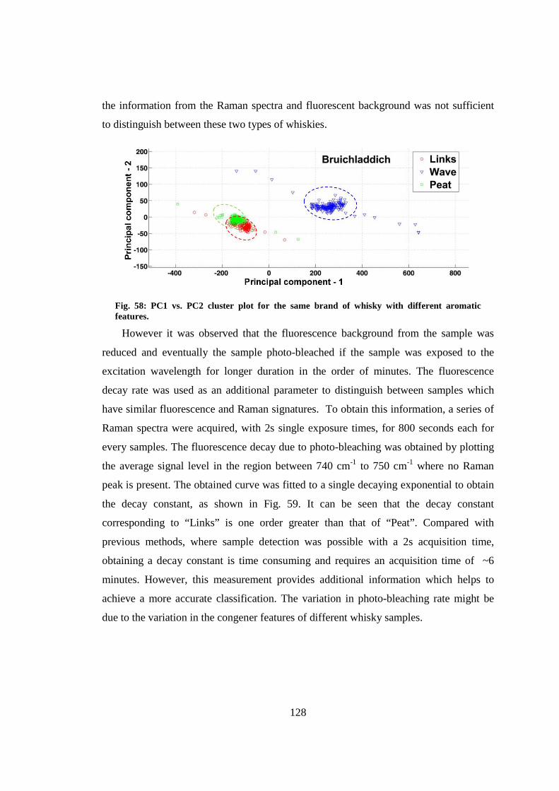
128
the information from the Raman spectra and fluorescent background was not sufficient
to distinguish between these two types of whiskies.
Fig. 58: PC1 vs. PC2 cluster plot for the same brand of whisky with different aromatic features.
However it was observed that the fluorescence background from the sample was
reduced and eventually the sample photo-bleached if the sample was exposed to the
excitation wavelength for longer duration in the order of minutes. The fluorescence
decay rate was used as an additional parameter to distinguish between samples which
have similar fluorescence and Raman signatures. To obtain this information, a series of
Raman spectra were acquired, with 2s single exposure times, for 800 seconds each for
every samples. The fluorescence decay due to photo-bleaching was obtained by plotting
the average signal level in the region between 740 cm-1 to 750 cm-1 where no Raman
peak is present. The obtained curve was fitted to a single decaying exponential to obtain
the decay constant, as shown in Fig. 59. It can be seen that the decay constant
corresponding to “Links” is one order greater than that of “Peat”. Compared with
previous methods, where sample detection was possible with a 2s acquisition time,
obtaining a decay constant is time consuming and requires an acquisition time of ~6
minutes. However, this measurement provides additional information which helps to
achieve a more accurate classification. The variation in photo-bleaching rate might be
due to the variation in the congener features of different whisky samples.
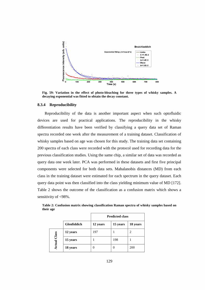
129
Fig. 59: Variation in the effect of photo-bleaching for three types of whisky samples. A decaying exponential was fitted to obtain the decay constant.
8.3.4 Reproducibility
Reproducibility of the data is another important aspect when such optofluidic
devices are used for practical applications. The reproducibility in the whisky
differentiation results have been verified by classifying a query data set of Raman
spectra recorded one week after the measurement of a training dataset. Classification of
whisky samples based on age was chosen for this study. The training data set containing
200 spectra of each class were recorded with the protocol used for recording data for the
previous classification studies. Using the same chip, a similar set of data was recorded as
query data one week later. PCA was performed in these datasets and first five principal
components were selected for both data sets. Mahalanobis distances (MD) from each
class in the training dataset were estimated for each spectrum in the query dataset. Each
query data point was then classified into the class yielding minimum value of MD [172].
Table 2 shows the outcome of the classification as a confusion matrix which shows a
sensitivity of <98%.
Table 2: Confusion matrix showing classification Raman spectra of whisky samples based on their age
Predicted class
Glenfiddich 12 years 15 years 18 years
Act
ual C
lass
12 years 197 1 2
15 years 1 198 1
18 years 0 0 200
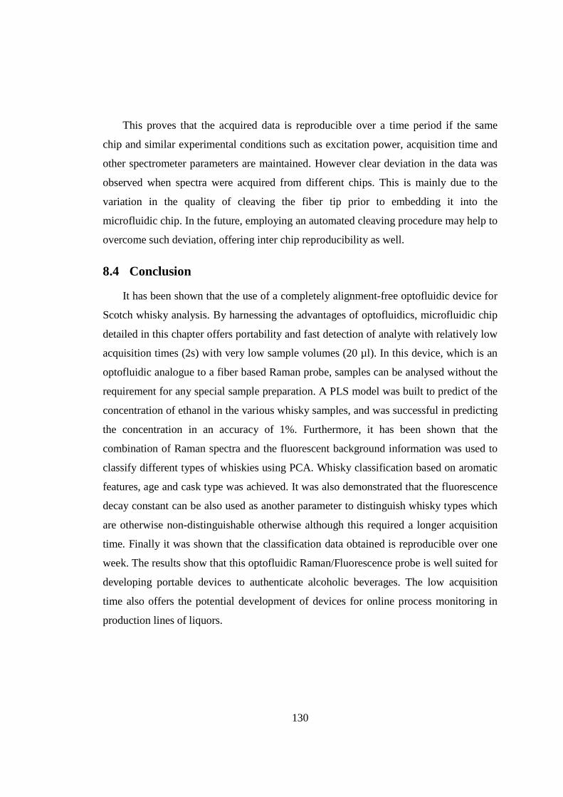
130
This proves that the acquired data is reproducible over a time period if the same
chip and similar experimental conditions such as excitation power, acquisition time and
other spectrometer parameters are maintained. However clear deviation in the data was
observed when spectra were acquired from different chips. This is mainly due to the
variation in the quality of cleaving the fiber tip prior to embedding it into the
microfluidic chip. In the future, employing an automated cleaving procedure may help to
overcome such deviation, offering inter chip reproducibility as well.
8.4 Conclusion
It has been shown that the use of a completely alignment-free optofluidic device for
Scotch whisky analysis. By harnessing the advantages of optofluidics, microfluidic chip
detailed in this chapter offers portability and fast detection of analyte with relatively low
acquisition times (2s) with very low sample volumes (20 µl). In this device, which is an
optofluidic analogue to a fiber based Raman probe, samples can be analysed without the
requirement for any special sample preparation. A PLS model was built to predict of the
concentration of ethanol in the various whisky samples, and was successful in predicting
the concentration in an accuracy of 1%. Furthermore, it has been shown that the
combination of Raman spectra and the fluorescent background information was used to
classify different types of whiskies using PCA. Whisky classification based on aromatic
features, age and cask type was achieved. It was also demonstrated that the fluorescence
decay constant can be also used as another parameter to distinguish whisky types which
are otherwise non-distinguishable otherwise although this required a longer acquisition
time. Finally it was shown that the classification data obtained is reproducible over one
week. The results show that this optofluidic Raman/Fluorescence probe is well suited for
developing portable devices to authenticate alcoholic beverages. The low acquisition
time also offers the potential development of devices for online process monitoring in
production lines of liquors.
131
Relevant publications
• Ashok PC, Praveen BB, Dholakia K (2011) Near infrared spectroscopic
analysis of single malt scotch whisky on an optofluidic chip. Opt Express 19
(23):22982-22992. doi:10.1364/OE.19.022982
Publicity
“Counterfeit whisky detection” aspect of this work has obtained media attention
worldwide during November, December 2011. (Due to the large volume specific news is
not cited here).
Contributions
P. C. Ashok designed and implemented the experiment. B. B. Praveen assisted PCA
in sample preparation and data processing.
132
9. Fabrication of microlens fiber combined with microfluidic gene delivery for integrated optical transfection
9.1 Introduction
The introduction of therapeutic and other agents into cells which are otherwise
membrane impermeable remains a key requirement in cell biology. Currently, there are a
variety of transfection methods used to solve this problem, including chemical, physical,
optical, electrical, and viral [173]. Among these, optical transfection is a technique
which offers selectivity, specificity, high transfection efficiency and good post-
transfection cell viability. By applying a tightly focused laser beam on the cell
membrane, optical transfection can transiently and locally increase the permeability of
the cell’s plasma membrane to allow, for example nucleic acids to be internalized.
Femtosecond (fs) laser assisted transfection has proven to be the most effective method
to date amongst the use of alternative laser systems with an excellent potential for
targeting single cells in vitro [174,175]. However most of the optical transfection
techniques that have been used employ free space (bulky) optical setups which limit the
potential application of the technology for in-vivo experiments. In addition, the
transfection efficiency achieved by such a setup is highly dependent on the quality of the
photoporation beam, so an expertise in optical alignment is necessary to achieve efficient
transfection. Therefore, to overcome these limitations, there is a need for the
development of fiber based optical transfection techniques.
A fiber based system offers not only compactness but also the advantage that once
the laser has been fiber coupled, no special optical alignment is required to perform
optical transfection. The only reported fiber based femtosecond optical transfection
technique to date uses an axicon tipped optical fiber for light delivery [176]. However
the Hydrogen Fluoride (HF) based etching makes the fabrication procedure of axicon
tips, hazardous and also the transfection efficiency is very sensitive to the quality of the
axicon tip. In addition, the short working distance produced by the axicon makes the
targeting of the beam focus at the cell membrane very difficult: particular care has to be
taken to make sure both fiber tip and cells are not damaged. A solution to the production
of a miniaturized fiber based optical transfection system is to fabricate a microlens at the
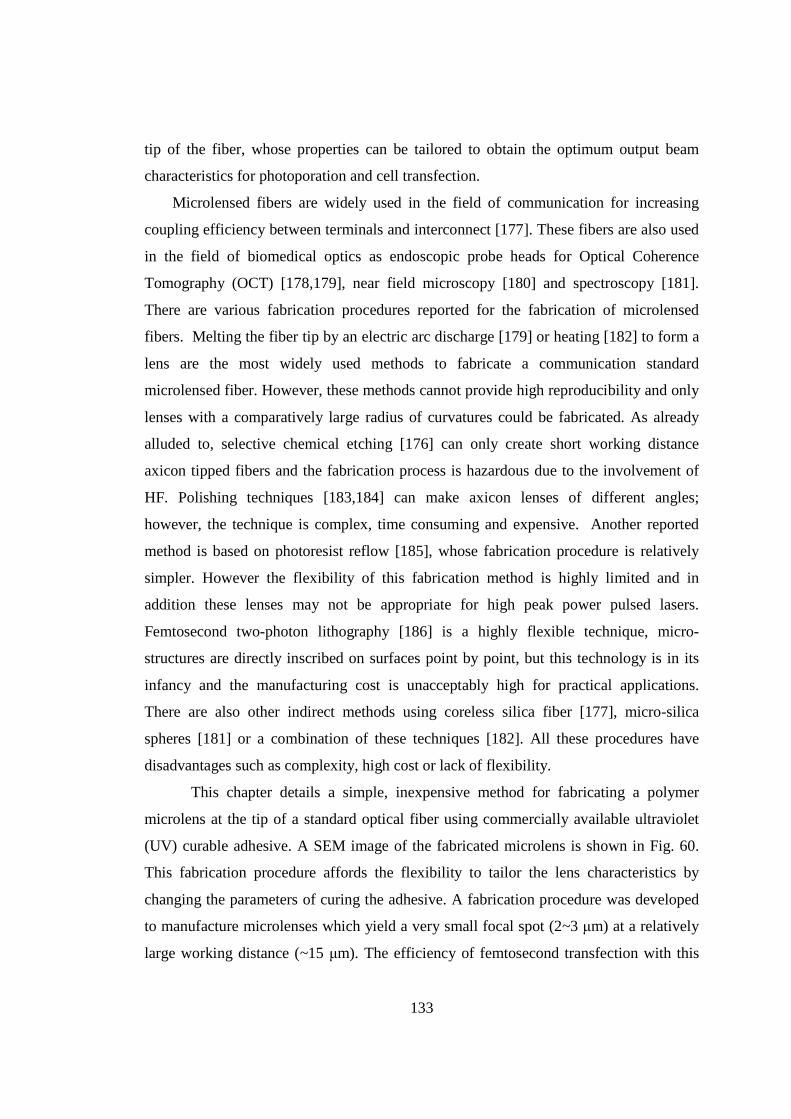
133
tip of the fiber, whose properties can be tailored to obtain the optimum output beam
characteristics for photoporation and cell transfection.
Microlensed fibers are widely used in the field of communication for increasing
coupling efficiency between terminals and interconnect [177]. These fibers are also used
in the field of biomedical optics as endoscopic probe heads for Optical Coherence
Tomography (OCT) [178,179], near field microscopy [180] and spectroscopy [181].
There are various fabrication procedures reported for the fabrication of microlensed
fibers. Melting the fiber tip by an electric arc discharge [179] or heating [182] to form a
lens are the most widely used methods to fabricate a communication standard
microlensed fiber. However, these methods cannot provide high reproducibility and only
lenses with a comparatively large radius of curvatures could be fabricated. As already
alluded to, selective chemical etching [176] can only create short working distance
axicon tipped fibers and the fabrication process is hazardous due to the involvement of
HF. Polishing techniques [183,184] can make axicon lenses of different angles;
however, the technique is complex, time consuming and expensive. Another reported
method is based on photoresist reflow [185], whose fabrication procedure is relatively
simpler. However the flexibility of this fabrication method is highly limited and in
addition these lenses may not be appropriate for high peak power pulsed lasers.
Femtosecond two-photon lithography [186] is a highly flexible technique, micro-
structures are directly inscribed on surfaces point by point, but this technology is in its
infancy and the manufacturing cost is unacceptably high for practical applications.
There are also other indirect methods using coreless silica fiber [177], micro-silica
spheres [181] or a combination of these techniques [182]. All these procedures have
disadvantages such as complexity, high cost or lack of flexibility.
This chapter details a simple, inexpensive method for fabricating a polymer
microlens at the tip of a standard optical fiber using commercially available ultraviolet
(UV) curable adhesive. A SEM image of the fabricated microlens is shown in Fig. 60.
This fabrication procedure affords the flexibility to tailor the lens characteristics by
changing the parameters of curing the adhesive. A fabrication procedure was developed
to manufacture microlenses which yield a very small focal spot (2~3 µm) at a relatively
large working distance (~15 µm). The efficiency of femtosecond transfection with this
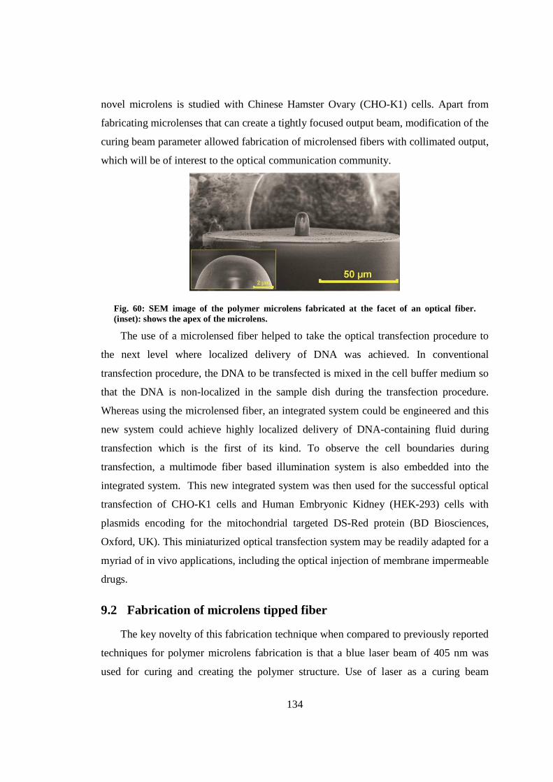
134
novel microlens is studied with Chinese Hamster Ovary (CHO-K1) cells. Apart from
fabricating microlenses that can create a tightly focused output beam, modification of the
curing beam parameter allowed fabrication of microlensed fibers with collimated output,
which will be of interest to the optical communication community.
Fig. 60: SEM image of the polymer microlens fabricated at the facet of an optical fiber. (inset): shows the apex of the microlens.
The use of a microlensed fiber helped to take the optical transfection procedure to
the next level where localized delivery of DNA was achieved. In conventional
transfection procedure, the DNA to be transfected is mixed in the cell buffer medium so
that the DNA is non-localized in the sample dish during the transfection procedure.
Whereas using the microlensed fiber, an integrated system could be engineered and this
new system could achieve highly localized delivery of DNA-containing fluid during
transfection which is the first of its kind. To observe the cell boundaries during
transfection, a multimode fiber based illumination system is also embedded into the
integrated system. This new integrated system was then used for the successful optical
transfection of CHO-K1 cells and Human Embryonic Kidney (HEK-293) cells with
plasmids encoding for the mitochondrial targeted DS-Red protein (BD Biosciences,
Oxford, UK). This miniaturized optical transfection system may be readily adapted for a
myriad of in vivo applications, including the optical injection of membrane impermeable
drugs.
9.2 Fabrication of microlens tipped fiber
The key novelty of this fabrication technique when compared to previously reported
techniques for polymer microlens fabrication is that a blue laser beam of 405 nm was
used for curing and creating the polymer structure. Use of laser as a curing beam
135
allowed modification of the curing beam profile, increasing flexibility to create the
desired shape of microlens specific for various applications.
The polymer microlens was fabricated onto the tip of a standard fiber by using a UV
curable adhesive, cured with a focused UV beam. The commercially available single
mode fiber had a mode field diameter of 5.6 µm, cladding diameter 125 µm, and an
operating wavelength of 830±100 nm (Thorlabs, SM800-5.6-125). A UV curable
adhesive (Norland, NOA 65) with optimum sensitivity for curing in the 350 – 380 nm
range was used as the photopolymer for fabrication of the microlens, due to its good
adhesion to glass, fast curing time, easy processing, suitable refractive index (1.524 for
polymerized resin) and high transmission efficiency (~98%) at 800 nm. These
characteristics make the polymer lens ideal for the delivery of high peak power pulsed
laser light without damaging the structure. A violet diode laser (Toptica Photonics
CVLS-LH050-2V1, λ=405 nm, maximum output power = 40 mW) was used as the
source to cure the UV adhesive. The custom made setup used for fabrication is shown in
Fig. 61.
Laser light was coupled through an objective (x10, Newport, UK) into a single
mode optical fiber (Thorlabs, S405-HP) with a coupling efficiency of ~45%, to improve
the lateral profile of the laser beam. The optical fiber was then carefully cleaved and the
facet was examined using SEM. The lateral beam profile of the output beam was
measured using a long working distance (WD) objective (Mitutoyo x100 infinity-
corrected, WD = 6mm ) to confirm a high quality TEM00 Gaussian beam profile. A very
high quality beam profile and optical alignment are essential for this lens fabrication
method. The laser beam was then directed to an objective (x60 Nikon) and focused near
the cleaved tip of an optical fiber, which was vertically mounted on an xyz translation
stage with 1 micrometer resolution. The cleaved tip of the fiber was imaged onto a CCD
camera (WAT-250D) to position the curing beam at the core of the fiber. The exposure
of the curing time was controlled by a shutter (Newport, UK, model 845HP-02).
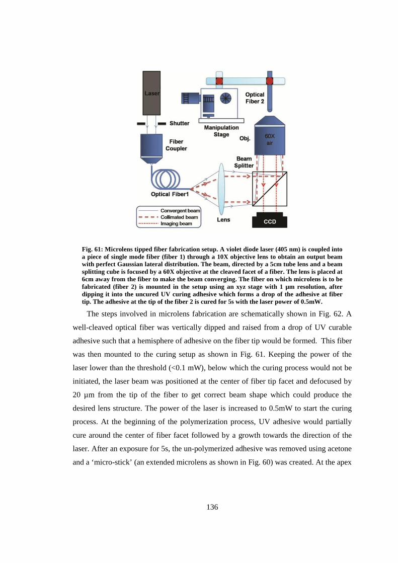
136
Fig. 61: Microlens tipped fiber fabrication setup. A violet diode laser (405 nm) is coupled into a piece of single mode fiber (fiber 1) through a 10X objective lens to obtain an output beam with perfect Gaussian lateral distribution. The beam, directed by a 5cm tube lens and a beam splitting cube is focused by a 60X objective at the cleaved facet of a fiber. The lens is placed at 6cm away from the fiber to make the beam converging. The fiber on which microlens is to be fabricated (fiber 2) is mounted in the setup using an xyz stage with 1 µm resolution, after dipping it into the uncured UV curing adhesive which forms a drop of the adhesive at fiber tip. The adhesive at the tip of the fiber 2 is cured for 5s with the laser power of 0.5mW.
The steps involved in microlens fabrication are schematically shown in Fig. 62. A
well-cleaved optical fiber was vertically dipped and raised from a drop of UV curable
adhesive such that a hemisphere of adhesive on the fiber tip would be formed. This fiber
was then mounted to the curing setup as shown in Fig. 61. Keeping the power of the
laser lower than the threshold (<0.1 mW), below which the curing process would not be
initiated, the laser beam was positioned at the center of fiber tip facet and defocused by
20 µm from the tip of the fiber to get correct beam shape which could produce the
desired lens structure. The power of the laser is increased to 0.5mW to start the curing
process. At the beginning of the polymerization process, UV adhesive would partially
cure around the center of fiber facet followed by a growth towards the direction of the
laser. After an exposure for 5s, the un-polymerized adhesive was removed using acetone
and a ‘micro-stick’ (an extended microlens as shown in Fig. 60) was created. At the apex
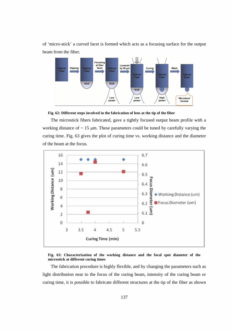
137
of ‘micro-stick’ a curved facet is formed which acts as a focusing surface for the output
beam from the fiber.
Fig. 62: Different steps involved in the fabrication of lens at the tip of the fiber
The microstick fibers fabricated, gave a tightly focused output beam profile with a
working distance of ~ 15 µm. These parameters could be tuned by carefully varying the
curing time. Fig. 63 gives the plot of curing time vs. working distance and the diameter
of the beam at the focus.
Fig. 63: Characterization of the working distance and the focal spot diameter of the microstick at different curing times
The fabrication procedure is highly flexible, and by changing the parameters such as
light distribution near to the focus of the curing beam, intensity of the curing beam or
curing time, it is possible to fabricate different structures at the tip of the fiber as shown
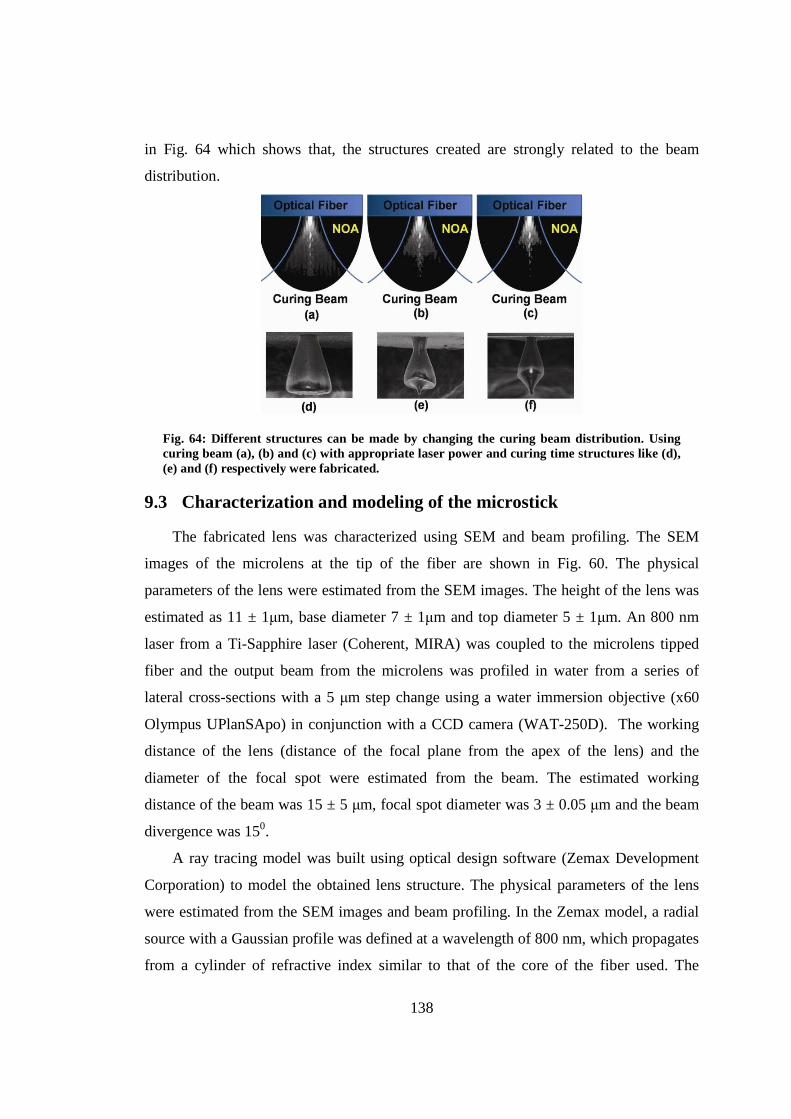
138
in Fig. 64 which shows that, the structures created are strongly related to the beam
distribution.
Fig. 64: Different structures can be made by changing the curing beam distribution. Using curing beam (a), (b) and (c) with appropriate laser power and curing time structures like (d), (e) and (f) respectively were fabricated.
9.3 Characterization and modeling of the microstick
The fabricated lens was characterized using SEM and beam profiling. The SEM
images of the microlens at the tip of the fiber are shown in Fig. 60. The physical
parameters of the lens were estimated from the SEM images. The height of the lens was
estimated as 11 ± 1µm, base diameter 7 ± 1µm and top diameter 5 ± 1µm. An 800 nm
laser from a Ti-Sapphire laser (Coherent, MIRA) was coupled to the microlens tipped
fiber and the output beam from the microlens was profiled in water from a series of
lateral cross-sections with a 5 µm step change using a water immersion objective (x60
Olympus UPlanSApo) in conjunction with a CCD camera (WAT-250D). The working
distance of the lens (distance of the focal plane from the apex of the lens) and the
diameter of the focal spot were estimated from the beam. The estimated working
distance of the beam was 15 ± 5 µm, focal spot diameter was 3 ± 0.05 µm and the beam
divergence was 150.
A ray tracing model was built using optical design software (Zemax Development
Corporation) to model the obtained lens structure. The physical parameters of the lens
were estimated from the SEM images and beam profiling. In the Zemax model, a radial
source with a Gaussian profile was defined at a wavelength of 800 nm, which propagates
from a cylinder of refractive index similar to that of the core of the fiber used. The
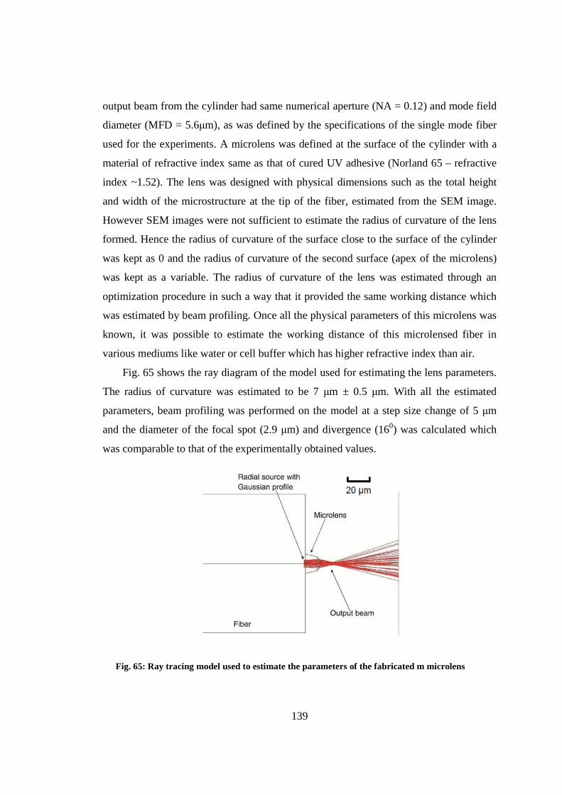
139
output beam from the cylinder had same numerical aperture (NA = 0.12) and mode field
diameter (MFD = 5.6µm), as was defined by the specifications of the single mode fiber
used for the experiments. A microlens was defined at the surface of the cylinder with a
material of refractive index same as that of cured UV adhesive (Norland 65 – refractive
index ~1.52). The lens was designed with physical dimensions such as the total height
and width of the microstructure at the tip of the fiber, estimated from the SEM image.
However SEM images were not sufficient to estimate the radius of curvature of the lens
formed. Hence the radius of curvature of the surface close to the surface of the cylinder
was kept as 0 and the radius of curvature of the second surface (apex of the microlens)
was kept as a variable. The radius of curvature of the lens was estimated through an
optimization procedure in such a way that it provided the same working distance which
was estimated by beam profiling. Once all the physical parameters of this microlens was
known, it was possible to estimate the working distance of this microlensed fiber in
various mediums like water or cell buffer which has higher refractive index than air.
Fig. 65 shows the ray diagram of the model used for estimating the lens parameters.
The radius of curvature was estimated to be 7 µm ± 0.5 µm. With all the estimated
parameters, beam profiling was performed on the model at a step size change of 5 µm
and the diameter of the focal spot (2.9 µm) and divergence (160) was calculated which
was comparable to that of the experimentally obtained values.
Fig. 65: Ray tracing model used to estimate the parameters of the fabricated m microlens
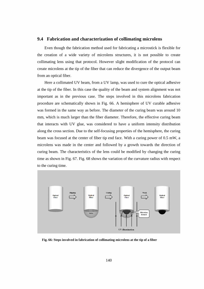
140
9.4 Fabrication and characterization of collimating microlens
Even though the fabrication method used for fabricating a microstick is flexible for
the creation of a wide variety of microlens structures, it is not possible to create
collimating lens using that protocol. However slight modification of the protocol can
create microlens at the tip of the fiber that can reduce the divergence of the output beam
from an optical fiber.
Here a collimated UV beam, from a UV lamp, was used to cure the optical adhesive
at the tip of the fiber. In this case the quality of the beam and system alignment was not
important as in the previous case. The steps involved in this microlens fabrication
procedure are schematically shown in Fig. 66. A hemisphere of UV curable adhesive
was formed in the same way as before. The diameter of the curing beam was around 10
mm, which is much larger than the fiber diameter. Therefore, the effective curing beam
that interacts with UV glue, was considered to have a uniform intensity distribution
along the cross section. Due to the self-focusing properties of the hemisphere, the curing
beam was focused at the center of fiber tip end face. With a curing power of 0.5 mW, a
microlens was made in the center and followed by a growth towards the direction of
curing beam. The characteristics of the lens could be modified by changing the curing
time as shown in Fig. 67. Fig. 68 shows the variation of the curvature radius with respect
to the curing time.
Fig. 66: Steps involved in fabrication of collimating microlens at the tip of a fiber
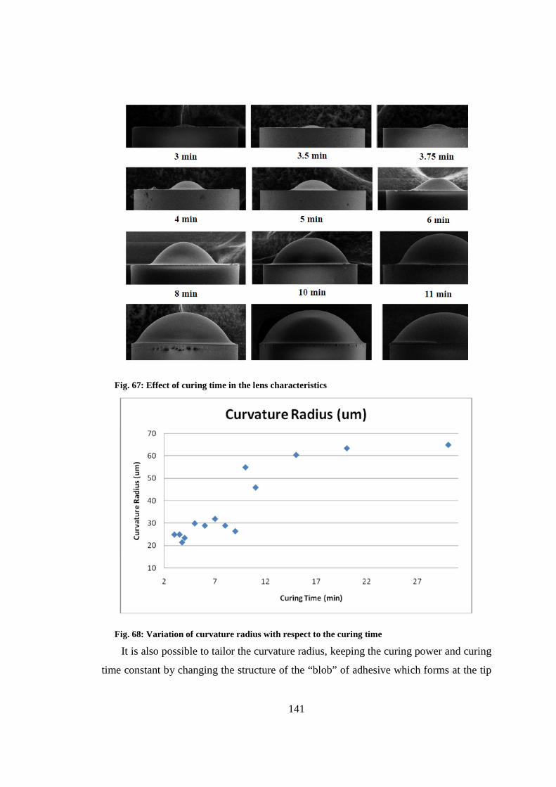
141
Fig. 67: Effect of curing time in the lens characteristics
Fig. 68: Variation of curvature radius with respect to the curing time
It is also possible to tailor the curvature radius, keeping the curing power and curing
time constant by changing the structure of the “blob” of adhesive which forms at the tip
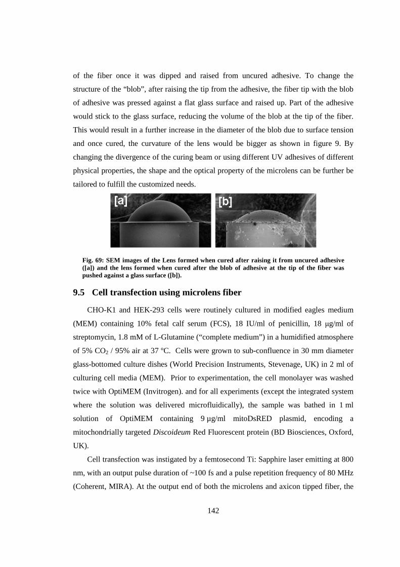
142
of the fiber once it was dipped and raised from uncured adhesive. To change the
structure of the “blob”, after raising the tip from the adhesive, the fiber tip with the blob
of adhesive was pressed against a flat glass surface and raised up. Part of the adhesive
would stick to the glass surface, reducing the volume of the blob at the tip of the fiber.
This would result in a further increase in the diameter of the blob due to surface tension
and once cured, the curvature of the lens would be bigger as shown in figure 9. By
changing the divergence of the curing beam or using different UV adhesives of different
physical properties, the shape and the optical property of the microlens can be further be
tailored to fulfill the customized needs.
Fig. 69: SEM images of the Lens formed when cured after raising it from uncured adhesive ([a]) and the lens formed when cured after the blob of adhesive at the tip of the fiber was pushed against a glass surface ([b]).
9.5 Cell transfection using microlens fiber
CHO-K1 and HEK-293 cells were routinely cultured in modified eagles medium
(MEM) containing 10% fetal calf serum (FCS), 18 IU/ml of penicillin, 18 µg/ml of
streptomycin, 1.8 mM of L-Glutamine (“complete medium”) in a humidified atmosphere
of 5% CO2 / 95% air at 37 ºC. Cells were grown to sub-confluence in 30 mm diameter
glass-bottomed culture dishes (World Precision Instruments, Stevenage, UK) in 2 ml of
culturing cell media (MEM). Prior to experimentation, the cell monolayer was washed
twice with OptiMEM (Invitrogen). and for all experiments (except the integrated system
where the solution was delivered microfluidically), the sample was bathed in 1 ml
solution of OptiMEM containing 9 µg/ml mitoDsRED plasmid, encoding a
mitochondrially targeted Discoideum Red Fluorescent protein (BD Biosciences, Oxford,
UK).
Cell transfection was instigated by a femtosecond Ti: Sapphire laser emitting at 800
nm, with an output pulse duration of ~100 fs and a pulse repetition frequency of 80 MHz
(Coherent, MIRA). At the output end of both the microlens and axicon tipped fiber, the
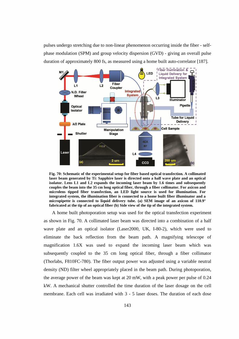
143
pulses undergo stretching due to non-linear phenomenon occurring inside the fiber - self-
phase modulation (SPM) and group velocity dispersion (GVD) - giving an overall pulse
duration of approximately 800 fs, as measured using a home built auto-correlator [187].
Fig. 70: Schematic of the experimental setup for fiber based optical transfection. A collimated laser beam generated by Ti: Sapphire laser is directed onto a half wave plate and an optical isolator. Lens L1 and L2 expands the incoming laser beam by 1.6 times and subsequently couples the beam into the 35 cm long optical fiber, through a fiber collimator. For axicon and microlens tipped fiber transfection, an LED light source is used for illumination. For integrated system, the illumination fiber is connected to a home built fiber illuminator and a micropipette is connected to liquid delivery tube. (a) SEM image of an axicon of 110.9° fabricated at the tip of an optical fiber (b) Side view of the tip of the integrated system.
A home built photoporation setup was used for the optical transfection experiment
as shown in Fig. 70. A collimated laser beam was directed into a combination of a half
wave plate and an optical isolator (Laser2000, UK, I-80-2), which were used to
eliminate the back reflection from the beam path. A magnifying telescope of
magnification 1.6X was used to expand the incoming laser beam which was
subsequently coupled to the 35 cm long optical fiber, through a fiber collimator
(Thorlabs, F810FC-780). The fiber output power was adjusted using a variable neutral
density (ND) filter wheel appropriately placed in the beam path. During photoporation,
the average power of the beam was kept at 20 mW, with a peak power per pulse of 0.24
kW. A mechanical shutter controlled the time duration of the laser dosage on the cell
membrane. Each cell was irradiated with 3 - 5 laser doses. The duration of each dose
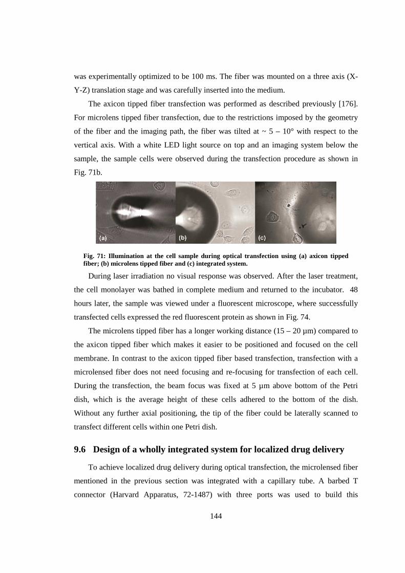
144
was experimentally optimized to be 100 ms. The fiber was mounted on a three axis (X-
Y-Z) translation stage and was carefully inserted into the medium.
The axicon tipped fiber transfection was performed as described previously [176].
For microlens tipped fiber transfection, due to the restrictions imposed by the geometry
of the fiber and the imaging path, the fiber was tilted at ~ 5 – 10° with respect to the
vertical axis. With a white LED light source on top and an imaging system below the
sample, the sample cells were observed during the transfection procedure as shown in
Fig. 71b.
Fig. 71: Illumination at the cell sample during optical transfection using (a) axicon tipped fiber; (b) microlens tipped fiber and (c) integrated system.
During laser irradiation no visual response was observed. After the laser treatment,
the cell monolayer was bathed in complete medium and returned to the incubator. 48
hours later, the sample was viewed under a fluorescent microscope, where successfully
transfected cells expressed the red fluorescent protein as shown in Fig. 74.
The microlens tipped fiber has a longer working distance (15 – 20 µm) compared to
the axicon tipped fiber which makes it easier to be positioned and focused on the cell
membrane. In contrast to the axicon tipped fiber based transfection, transfection with a
microlensed fiber does not need focusing and re-focusing for transfection of each cell.
During the transfection, the beam focus was fixed at 5 µm above bottom of the Petri
dish, which is the average height of these cells adhered to the bottom of the dish.
Without any further axial positioning, the tip of the fiber could be laterally scanned to
transfect different cells within one Petri dish.
9.6 Design of a wholly integrated system for localized drug delivery
To achieve localized drug delivery during optical transfection, the microlensed fiber
mentioned in the previous section was integrated with a capillary tube. A barbed T
connector (Harvard Apparatus, 72-1487) with three ports was used to build this
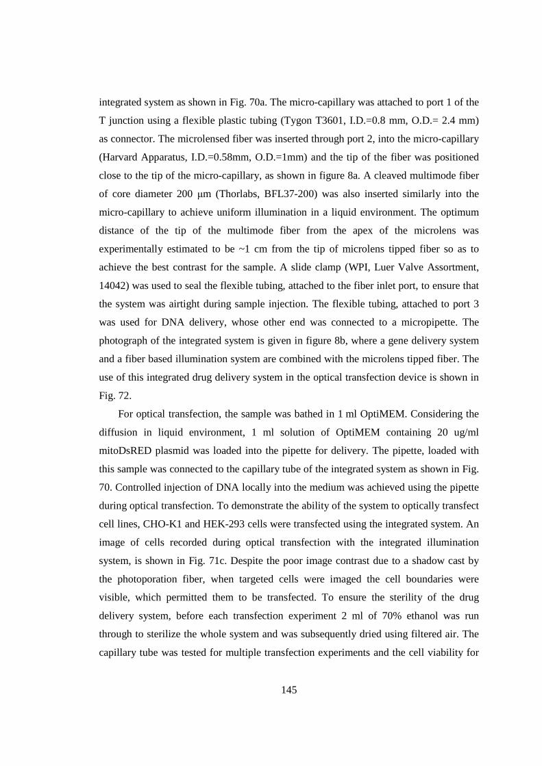
145
integrated system as shown in Fig. 70a. The micro-capillary was attached to port 1 of the
T junction using a flexible plastic tubing (Tygon T3601, I.D.=0.8 mm, O.D.= 2.4 mm)
as connector. The microlensed fiber was inserted through port 2, into the micro-capillary
(Harvard Apparatus, I.D.=0.58mm, O.D.=1mm) and the tip of the fiber was positioned
close to the tip of the micro-capillary, as shown in figure 8a. A cleaved multimode fiber
of core diameter 200 µm (Thorlabs, BFL37-200) was also inserted similarly into the
micro-capillary to achieve uniform illumination in a liquid environment. The optimum
distance of the tip of the multimode fiber from the apex of the microlens was
experimentally estimated to be ~1 cm from the tip of microlens tipped fiber so as to
achieve the best contrast for the sample. A slide clamp (WPI, Luer Valve Assortment,
14042) was used to seal the flexible tubing, attached to the fiber inlet port, to ensure that
the system was airtight during sample injection. The flexible tubing, attached to port 3
was used for DNA delivery, whose other end was connected to a micropipette. The
photograph of the integrated system is given in figure 8b, where a gene delivery system
and a fiber based illumination system are combined with the microlens tipped fiber. The
use of this integrated drug delivery system in the optical transfection device is shown in
Fig. 72.
For optical transfection, the sample was bathed in 1 ml OptiMEM. Considering the
diffusion in liquid environment, 1 ml solution of OptiMEM containing 20 ug/ml
mitoDsRED plasmid was loaded into the pipette for delivery. The pipette, loaded with
this sample was connected to the capillary tube of the integrated system as shown in Fig.
70. Controlled injection of DNA locally into the medium was achieved using the pipette
during optical transfection. To demonstrate the ability of the system to optically transfect
cell lines, CHO-K1 and HEK-293 cells were transfected using the integrated system. An
image of cells recorded during optical transfection with the integrated illumination
system, is shown in Fig. 71c. Despite the poor image contrast due to a shadow cast by
the photoporation fiber, when targeted cells were imaged the cell boundaries were
visible, which permitted them to be transfected. To ensure the sterility of the drug
delivery system, before each transfection experiment 2 ml of 70% ethanol was run
through to sterilize the whole system and was subsequently dried using filtered air. The
capillary tube was tested for multiple transfection experiments and the cell viability for
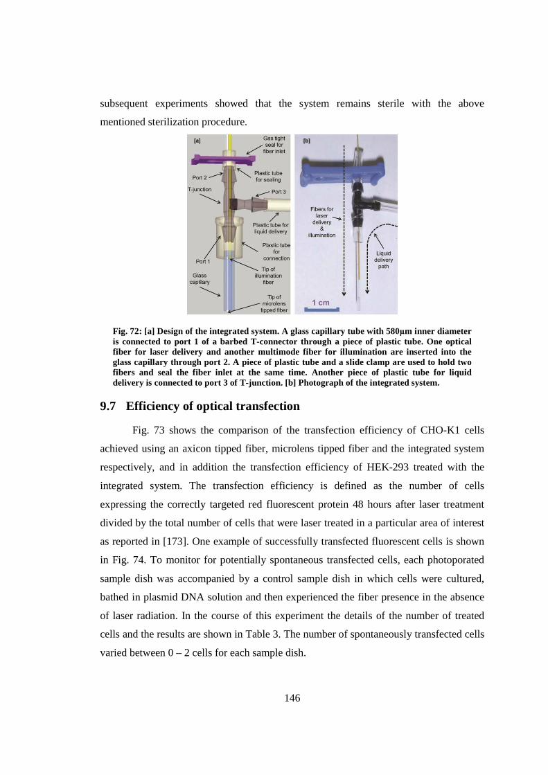
146
subsequent experiments showed that the system remains sterile with the above
mentioned sterilization procedure.
Fig. 72: [a] Design of the integrated system. A glass capillary tube with 580µm inner diameter is connected to port 1 of a barbed T-connector through a piece of plastic tube. One optical fiber for laser delivery and another multimode fiber for illumination are inserted into the glass capillary through port 2. A piece of plastic tube and a slide clamp are used to hold two fibers and seal the fiber inlet at the same time. Another piece of plastic tube for liquid delivery is connected to port 3 of T-junction. [b] Photograph of the integrated system.
9.7 Efficiency of optical transfection
Fig. 73 shows the comparison of the transfection efficiency of CHO-K1 cells
achieved using an axicon tipped fiber, microlens tipped fiber and the integrated system
respectively, and in addition the transfection efficiency of HEK-293 treated with the
integrated system. The transfection efficiency is defined as the number of cells
expressing the correctly targeted red fluorescent protein 48 hours after laser treatment
divided by the total number of cells that were laser treated in a particular area of interest
as reported in [173]. One example of successfully transfected fluorescent cells is shown
in Fig. 74. To monitor for potentially spontaneous transfected cells, each photoporated
sample dish was accompanied by a control sample dish in which cells were cultured,
bathed in plasmid DNA solution and then experienced the fiber presence in the absence
of laser radiation. In the course of this experiment the details of the number of treated
cells and the results are shown in Table 3. The number of spontaneously transfected cells
varied between 0 – 2 cells for each sample dish.
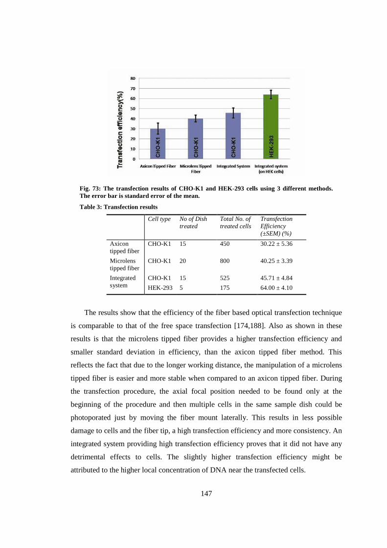
147
Fig. 73: The transfection results of CHO-K1 and HEK-293 cells using 3 different methods. The error bar is standard error of the mean.
Table 3: Transfection results
Cell type No of Dish treated
Total No. of treated cells
Transfection Efficiency (±SEM) (%)
Axicon tipped fiber
CHO-K1 15 450 30.22 ± 5.36
Microlens tipped fiber
CHO-K1 20 800 40.25 ± 3.39
Integrated system
CHO-K1 15 525 45.71 ± 4.84
HEK-293 5 175 64.00 ± 4.10
The results show that the efficiency of the fiber based optical transfection technique
is comparable to that of the free space transfection [174,188]. Also as shown in these
results is that the microlens tipped fiber provides a higher transfection efficiency and
smaller standard deviation in efficiency, than the axicon tipped fiber method. This
reflects the fact that due to the longer working distance, the manipulation of a microlens
tipped fiber is easier and more stable when compared to an axicon tipped fiber. During
the transfection procedure, the axial focal position needed to be found only at the
beginning of the procedure and then multiple cells in the same sample dish could be
photoporated just by moving the fiber mount laterally. This results in less possible
damage to cells and the fiber tip, a high transfection efficiency and more consistency. An
integrated system providing high transfection efficiency proves that it did not have any
detrimental effects to cells. The slightly higher transfection efficiency might be
attributed to the higher local concentration of DNA near the transfected cells.
148
Fig. 74: Fluorescent microscope image of optically transfected CHO-K1 cells, incubated for 48 hours after transfection. The bright cells are transfected successfully resulting in the uptake of the plasmid and thereby expressing the mitochondrially targeted red fluorescent protein.
9.8 Conclusion
This chapter detailed a simple method to fabricate a polymer microlens at the tip of
optical fiber and this technique has flexibility to allow the fabrication of customized
microlenses for specific applications. The technique was used to fabricate a ‘micro-stick’
which can produce a tightly focused beam (~3 µm focal diameter) at a comparatively
large working distance (~15 µm). Even though the stability requirement in this setup is
high, this protocol is much easier and flexible compared to other techniques [176] to
create a microlens to focus the output beam from an optical fiber. Also the optical
quality of the cured UV adhesive was good, so that it was possible to use such
microlensed fibers in applications which involve ultra-short laser pulses [189]. The
fabricated fiber was characterized using SEM imaging, beam profiling and a ray tracing
model; the parameters of the fabricated lens were estimated.
The fabrication of the collimating lens is simpler and does not require any
specialized optical alignment. However it offers the flexibility to fabricate a wide range
of microlenses depending on the application.
The fabrication procedure does not require any complex and expensive apparatus.
Also it has been observed that this fabrication procedure is highly reproducible as all the
149
parameters in the fabrication process are controllable and not sensitive to the
environment. The prospect of fabricating cheap polymer microlensed fiber would have
potential applications in the field of communication, bio-imaging, laser nano-surgery,
optical micro manipulation amongst others.
Furthermore this microstick tipped fiber was used for optical transfection of CHO-
K1 and HEK-293 cells and the transfection efficiency achieved was comparable to that
of conventional free space optical transfection setups and notably better than the
previously reported axicon tipped fiber based optical transfection. In addition, a novel
integrated system was developed to achieve localized drug (gene) delivery during
transfection by combining the microlens tipped fiber with a micro-capillary system. A
multimode fiber based illumination system was also combined with this integrated
system to allow the efficient visual identification of the cell boundaries during optical
transfection. This new technique opens up the prospect for a portable “hand-held”
system that can locally deliver therapeutic agents and transfect cells within a fiber
geometry placing minimal requirements upon any microscope system. This study may
lead towards a wholly fiber based photoporation free system on a microscope free
platform which would be compatible with endoscopic system to achieve in vivo optical
transfection.
Relevant publications
• Ma N, Ashok PC, Stevenson DJ, Gunn-Moore FJ, Dholakia K (2010)
Integrated optical transfection system using a microlens fiber combined with
microfluidic gene delivery. Biomed Opt Express 1 (2):694-705
• Ma N, Ashok PC, Gunn-Moore FJ, Dholakia K (2010) Fabrication of
polymer microlens at the apex of optical fiber. Paper presented at the
Photonics 2010, Guwahati, India.
Patent
• Application: The University of St. Andrews, Ma N, Ashok PC, Stevenson
DJ, Dholakia K, Gunn-Moore FJ, “ Microlensed fiber based poration” UK
Patent application No. GB1009800.2
150
Contributions
PCA and NM came up with the idea of microlensed fabrication and design of the
integrated optical transfection system. NM setup the experimental system for microlens
fabrication and performed optical transfection experiments. KD and DJS gave advice
regarding the design of integrated optical transfection system. FJG provided advice on
the optical transfection experiments.
151
10. Conclusions & Future Outlook
10.1 Summary of the thesis
The work presented in this thesis mainly focuses on developing optofluidic
technologies for sorting and sensing with a special aim to make the optics part of it
miniaturized and alignment free. Leak-proof embedding of optical fiber into a PDMS
based microfluidic chip facilitated the production of devices for sorting and sensing
applications. Although integration of optical technologies to microfluidics was the
common theme of this thesis, the areas of application in the studies detailed here vary.
Hence each chapter was treated as a stand-alone with its own introductory literature
review which discussed the state of the art in that particular field.
Chapter 1 of the thesis summarized the structure of this thesis. As mentioned in
Chapter 1, studies detailed in this thesis may be broadly categorized into three themes –
microfabrication techniques, passive optical cell fractionation, fiber based microfluidic
Raman spectroscopy.
Chapter 2 gave a general introduction to the physics that governs fluid dynamics at
micrometer scale along with a discussion on microfabrication techniques used for the
studies detailed in this chapter. The special characteristics of laminar flow of fluids at a
low Reynolds number was discussed along with introduction of dimensionless numbers
such as the Reynolds number and the Peclet number, that should be taken into
consideration while designing microfluidic devices. This was followed by a discussion
on the soft-lithography based fabrication technique which was used for fabricating
majority of the optofluidic devices that are discussed in this thesis. Various steps
involved in microfluidic chip fabrication, from concept to mold to the final chip, were
discussed in details. While this forms the general soft-lithography fabrication protocol,
modification of this protocol was required to achieve integration or incorporation of
optical technologies into the microfluidic chips. Various techniques developed for such
customized applications were discussed along with the details of a technique to fabricate
thermally actuated paraffin microvalves.
Chapter 3 began the discussion on the passive optical sorting techniques. Within
Chapter 3 was discussed the implementation of an optofluidic chip to perform optical
152
chromatography, a passive optical fractionation technique. In optical chromatography,
the interplay between optical radiation force and viscous drag force enables the
fractionation of colloids and cells based on its size, shape or refractive index. Unlike its
previous embodiments, where the laser beam was delivered into the microfluidic chip
through free-space coupling, here an embedded LMA-PCF was used to deliver a
fractionation beam into the microfluidic chip. The use of LMA-PCF ensured that the
beam profile of the laser beam which was delivered into the microfluidic channel
satisfied the necessary condition of low divergence which was necessary to achieve
optical chromatographic fractionation. The LMA-PCF could be embedded into the
microfluidic channel and to avoid fluid getting into the holes of PCF due to capillary
action, a novel capping procedure was developed. Further, the endlessly single mode
characteristics of LMA-PCF was used to couple a laser beam with wavelength 532 nm
along with the fractionation beam at wavelength 1064 nm to achieve simultaneous on-
chip fluorescent excitation and fractionation. The device was then characterized to
observe that the performance of this system is comparable to that of its previous free-
space variants. Along with refractive index driven and size driven separation of colloids
fractionation of cells was also demonstrated using this optofluidic device.
Chapter 4 discussed another approach for passive optical fractionation. Optical
fractionation of colloidal samples within a periodic optical landscape is a well-
established technique, and has been demonstrated previously at a proof of principle level
in several published literatures [77,31,190]. The work discussed in chapter 4, looked into
upgrading this technique to achieve the fractionation of cells. A passive optical sorting
device which sorts cells using a periodic optical landscape can be developed by
combining a microfluidic platform with an optical trapping system which can create an
optical landscape using multiple optical traps. This chapter described in detail the
construction and implementation of an optical trapping system capable of generating
time-shared multiple optical traps using DA-AOD. Along with the optical design of such
a system the development of a LabVIEW based interface to control this system, is
discussed in detail. This chapter further visited the basic theory of colloidal fractionation
using periodic optical landscape. There were four parameters which have to be
optimized to obtain selective deflection of one type of colloids to achieve fractionation
153
of a binary mixture of colloids. This numerical model may be used to find the optimum
set of parameters that can be used to achieve efficient fractionation. However this
approach would not work to fractionate cellular samples. The non-spherical shape of the
cell along with the lack of knowledge about the absolute size and refractive index of the
cell makes it impossible to use the numerical model to find the right set of parameters to
achieve efficient sorting. A calibration method was proposed to overcome this limitation.
In this approach, using a drag force measurement, the escape velocity of the cell, which
is the flow velocity at which the cell would escape from the optical trap, can be
estimated. This information can be used to find a spherical colloidal analogue to the cell,
which would interact similarly to that of the optical field while in a flow system. This
method could be used to assess the feasibility of fractionating two types of cells. If it is
feasible, the optimum set of parameters for the device to achieve efficient fractionation
may be obtained.
Chapter 5 moved towards the theme of spectroscopic sensing in optofluidics. More
specifically implementation of the technique of Raman spectroscopy for analyte
detection in microfluidics was discussed in chapters 5 to 8. Although Raman
spectroscopy has been used as a powerful detection modality in conjunction with
microfluidic over last 10 years, the implementation of this was limited to use of a bulk
Raman detection system which was used to probe samples in microfluidic channel from
outside. The optical alignment requirement and the background from the substrate, while
probing from outside, had remained a limitation of this approach. The work presented in
chapter 5 marked a transition of this technique to a fiber based detection scheme, where
the fiber probe was embedded into a microfluidic chip and was used for detecting
Raman spectra from the analyte. Unlike conventional fiber probe designs, a novel split
Raman probe, which is relatively easy to fabricate and relatively cheap, was used in this
embodiment of microfluidic Raman spectroscopy device. Along with characterization of
the device and identification of the optimized geometry, the ability of this technique to
detect bio-analytes was demonstrated by detecting urea within physiologically relevant
limits.
Although the optofluidic device discussed in chapter 5 succeeded to achieve a
completely alignment-free fiber based Raman spectroscopic detection, the physical
154
dimension of the split Raman probe made it impossible to scale down this technology to
true microfluidic dimensions. Chapter 6 moved towards the next generation of fiber
based microfluidic Raman spectroscopy device. The technology which enabled this was
called WCRS, and was realized by embedding two multimode optical fibers into a
microfluidic chip, one for Raman excitation and the other for Raman signal collection.
These fibers were oriented orthogonally to each other in such a way that the apex of
these fibers was at a distance in the order of the core size of these fibers. This allowed
localized collection of Raman signal avoiding any background from the substrate of the
microfluidic chip. The prospect of implementing WCRS without any filters at the tip of
the fiber made it possible to scale down the size of the fluidic channel to true
microfluidic dimensions. This device could be considered as an optofluidic analogue of
fiber Raman probe. However WCRS based optofluidic chip would be at least two orders
of magnitude cheaper and could be used to detect very low volume of analytes, in the
order of few microliters. Also the scalability of this technology enabled it to be
combined with other microfluidic functional devices. The applicability of WCRS
technology was demonstrated through experiments on bio-analyte detection, process
monitoring in micro-reactors and detection of contents in microdroplets.
The WCRS technology is a general architecture which allows flexibility to be
combined with advanced Raman spectroscopic techniques to enhance its sensitivity.
Chapter 7 discussed such an example, where a wavelength modulation based fluorescent
suppression technique was implemented in a WCRS based microfluidic chip. It was
shown using this technique that a seven fold enhancement in bio-analyte detection
sensitivity could be achieved in a WCRS based microfluidic device.
Chapter 8 discussed a more practical application of the WCRS based optofluidic
probe. The suitability of this device to analyze alcoholic beverages was demonstrated by
analyzing single malt Scotch whisky samples. It was possible to detect spectroscopic
information from whisky samples within a 2 s acquisition time with just 20 µl of sample
without any special sample preparation stage. From this information, with the help of
multivariate calibration technique – PLS – the ethanol content in the whisky samples
could be measired to 1% accuracy. Further multivariate classification technique – PCA –
155
was used to classify various whisky samples based on its aromatic features, age and
cask.
The focus of the study presented in chapter 9 differs from the ones presented in
previous chapters. This chapter discussed a novel microfabrication technique to fabricate
a polymer microlens at the tip of the fiber. The use of a UV laser with a tailored beam
profile to cure hemispherical UV glue made this a highly flexible technique, which is
relatively inexpensive to implement. A special microlensed fiber fabricated using this
technique was used to deliver a focused femto-second laser beam at a cell membrane to
perform fiber based optical transfection. This special fiber was combined with a
capillary microfluidic channel to achieve a probe which can perform optical transfection
with localized gene delivery.
10.2 Future outlook
This section holds a discussion on the future outlook on the general theme of this
thesis followed by short discussions on each of the technologies detailed in this thesis.
As mentioned before the common theme of this thesis is to make the optics part of
optofluidic technologies miniaturized and alignment-free. Various works presented in
this thesis demonstrated leak-proof embedding of optical waveguides into optofluidic
chips as one possible solution to this issue. Although similar approaches have been
demonstrated previously, this is the first time a geometry was realized in such a way that
the optical fibers were directly embedded into the microfluidic channel which avoided
optical aberration or background from the substrate material that separate the fiber
insertion channel from the microfluidic channels. Hence this approach could be
successfully implemented for optical fractionation application and Raman spectroscopic
sensing. Although the optical systems such as lasers and spectrometers used in these
works were bulk, laboratory grade ones, it is trivial to replace them with portable
components which are already available commercially. This can lead to optofluidic
based portable devices, suitable for field applications. And since the fiber is pre-aligned
in the fiber insertion channel, no optical alignment expertise would be required to
operate such devices. The prospect of implementing such devices into PDMS chips,
fabricated using soft-lithography technique, would help to reduce the cost of such
156
devices. Similar approaches could also be implemented for other sensing or
manipulation techniques as well. The commercial availability of a wide choice of optical
fibers, including custom made photonic crystal fibers, offers a variety of opportunities to
develop further embedded fiber based optofluidic devices for various applications.
10.2.1 Optical chromatography
The work presented in chapter 3 demonstrated the feasibility of implementing
optical chromatography in a microfluidic chip with a beam delivery using an embedded
fiber. LMA-PCF proved to be the ideal choice for beam delivery. Mainly the
fractionation of colloids was demonstrated in this work. As discussed in chapter 4, while
attempting to fractionate cellular samples using a passive optical fractionation technique,
a feasibility study will be required to identify the samples which can be fractionated with
this particular technology. This is true for the case of optical chromatography as well.
While it was trivial to fractionate cellular samples with and without an engulfed
polystyrene bead, further exploration is required to find samples that are suitable for
fractionation in this device without the need of a refractive index contrast enhancement
using dielectric tagging. In short, although optical chromatography is a promising optical
fractionation technique, to identify the samples that are feasible to be fractionated by this
technique is crucial for the future of this technology.
On the technical side, it is possible to tailor this device with the use of specialized
fibers that are capable of generating novel optical fields such as Bessel beams [191].
Such a combination might result in devices that would be able to achieve fractionation of
particles that would not be possible with conventional mildly focused Gaussian beams.
10.2.2 Periodic optical landscape based passive optical cell sorting
The work detailed in chapter 4 is the first stage of work towards developing an
optofluidic system capable of achieving passive optical fractionation of cells. While the
state of the art in this technology is able to achieve sensitive fractionation of colloidal
particles, implementing cellular fractionation using this technology poses several
challenges. Along with implementing an optical trapping system with an interface
tailored for this fractionation application, the theoretical challenges for achieving cellular
157
fractionation were also identified. The lack of knowledge about parameters such as the
absolute size and refractive index of cellular species, made it impossible to directly use
an already developed theory to find the optimum parameters to achieve cellular
fractionation. Therefore a calibration procedure was proposed to find a spherical
colloidal equivalent to a cellular species. This would make it possible to use the already
known theory for cellular samples as well to find the system’s parameters to achieve
fractionation. Experiments should be performed to validate the applicability of this
calibration procedure. Once proved, this procedure may open up opportunities to achieve
efficient passive optical cell sorting. Once such a technique is developed, it can find
applications in a wide variety of fields such as in microbiology and biotechnology, to
address a variety of high priority problems that could not be addressed with existing
active sorting techniques.
10.2.3 WCRS
The second generation of fiber based microfluidic Raman spectroscopy technology
– WCRS – has already proven to be useful for a variety of application, ranging from
analyte detection to online process monitoring. Although several proof of concept
experiments were demonstrated, further engineering is required to convert this
technology into an actual device. One of the factors which require engineering is
implementing a miniaturized laser and detection system. This would not be technically
challenging as there are already portable Raman lasers and spectrometers available in the
market. A combination of a WCRS based optofluidic chip with such a portable optical
device would make the whole system a truly portable system, suitable for field
applications.
The WCRS based optofluidic chip could be developed as an optofluidic analogue to
fiber Raman probes. The use of such a system for whisky detection was demonstrated. In
principle, this device can be used to detect counterfeit whisky samples and could be used
for benchmarking the quality of a particular whisky sample. While this could be one of
the applications of this technology, it could also be used for applications in other fields,
for example in environmental sensing technology. A portable WCRS device could be
158
used for detecting environmental contaminants like polycyclic aromatic hydrocarbons
(PAHs).
10.2.4 Polymer microlensed fiber fabrication
The technique of polymer microlensed fabrication discussed in chapter 9 is a
flexible and relatively inexpensive technique. A wide variety of structures at the tip of
optical fibers may be realized using this technique, making it a promising fabrication
method to be used in a variety of applications. Recently, the field of biomedical optics
has started using microlensed fibers for the endoscopic imaging and spectroscopic
analysis. Hence my novel microlensed fiber fabrication protocol may be useful for
developing novel endoscopic probes for in vivo imaging and disease diagnosis.
10.3 Conclusion
The technological advancements described in this thesis have proved that
optofluidic techniques hold a crucial role in the fields of biomedical research and
biochemical analytic detection. However, the optofluidic technologies still have to
mature from a proof of principle level, to devices suitable for practical applications; but,
integration and miniaturization of the optics part of optofluidics and making it
alignment-free is an essential step to push the technology towards this transition. The
studies detailed in the thesis, paves the way towards such a transition in integration.
159
Appendix 1 – Cell Preparation Protocols for the Optical Chromatography Experiments
Protocol for the photo-transfection of HEK-293 cells
HEK-293 cells, maintained in minimum essential medium (MEM), 1% penicillin-
streptomycin supplemented with 10% fetal bovine serum (FBS) (complete medium)
were grown in T25 vented top culture flasks and sub-cultured twice weekly at a ratio
1:4. The cells were incubated at 370C, 5% carbon dioxide and 85% humidity (optimum
growth conditions). Before photo-transfection, approximately 104 of cells in 2ml of
complete medium were seeded in 35mm diameter type zero glass bottomed Petri dishes.
These were incubated to sub-confluency over 24 hours under optimum growth
conditions. Following incubation, the monolayer was washed twice with 2ml of
OptiMEM each time, to remove the serum. Thereafter the cells were submerged in 60µl
of serum-free MEM containing 10µg/ml of pDsRed2-Mito plasmid deoxyribonucleic
acid (pDNA). Targeted photo-transfection of individual cells was then performed with a
femtosecond (fs) pulsed Ti:sapphire laser at central wavelength of 790nm, pulse
duration 200fs, pulse repetition frequency of 80MHz, 1.1 diameter focal spot with
60mW optical power and an exposure time of 40ms. Following laser irradiation, the
DNA-containing medium was aspirated and the monolayer washed once with OptiMEM.
2 ml of the complete medium was then added and the cells incubated under optimum
growth conditions for 48 hours before live cell fluorescence imaging.
Protocol for the incubation of HEK-293 cells with microspheres
Before their incubation with microspheres, the cells were grown at 37oC with 5%
CO2 and 85% humidity (optimum growth conditions). The experimental procedure for
incubating the adherent HEK-293 cells with the 2µm polymer spheres involved seeding
approximately 105 cells in 2ml complete medium onto sterile 30mm diameter culture
plates prior to microsphere treatment. These cells were grown to sub-confluency
overnight within optimum growth conditions. The following day (~ 24 hours post
plating), 2ml of culture supernatant that was left on top of the samples was aspirated and
replaced with the same volume of media containing 2µm diameter spheres. Hard-dyed
(internally dyed) red fluorescing polymer microspheres (Duke Scientific) were used
160
which have the dye incorporated throughout the polymer matrix (and so are not easily
quenched) with a 2µm diameter. The microspheres were made of polystyrene with a
density of 1.05g/cm3 and a refractive index of 1.59This type of fluorescent microsphere
was used as they emit a bright distinctive red color with an improved contrast and
visibility relative to the background material thus providing easy detection. These
spheres had an excitation maximum at 542nm and an emission maximum of 612nm.
Their original stock concentration was 2.3x10⁹ spheres/ml (solid 1%). For experimental
purposes, these were then further diluted 1:1000 in the complete growth media
depending on the cell line being investigated. After 24 hours of incubation, when the cell
line shows maximum internalization of 2µm spheres [20], the sample is used for
experiments.
161
Bibliography
1. Squires TM, Quake SR (2005) Microfluidics: Fluid physics at the nanoliter scale. Reviews of Modern Physics 77 (3):977-1026.
2. Whitesides GM (2006) The origins and the future of microfluidics. Nature 442 (7101):368-373.
3. Erickson D, Li D (2004) Integrated microfluidic devices. Analytica Chimica Acta 507 (1):11-26.
4. Daw R, Finkelstein J (2006) Lab on a chip. Nature 442 (7101):367-367.
5. Purcell EM (1977) Life at low reynolds number. American Journal of Physics 45 (1):3-11.
6. Famous last words (2011). Lab Chip 11 (13):2133-2134.
7. McDonald JC, Duffy DC, Anderson JR, Chiu DT, Wu H, Schueller OJA, G. M. Whitesides (2000) Fabrication of microfluidic systems in poly(dimethylsiloxane). Electrophoresis 21 (1):27-40.
8. Brody JP, Yager P, Goldstein RE, Austin RH (1996) Biotechnology at low reynolds numbers. Biophys J 71 (6):3430-3441.
9. Reynolds O (1883) An experimental investigation of the circumstances which determine whether the motion of water shall be direct or sinuous, and of the law of resistance in parallel channels. Philosophical Transactions of the Royal Society of London 174 (ArticleType: research-article / Full publication date: 1883 / Copyright © 1883 The Royal Society):935-982.
10. Weigl BH, Bardell RL, Cabrera CR (2003) Lab-on-a-chip for drug development. Advanced Drug Delivery Reviews 55 (3):349-377.
11. Duffy DC, McDonald JC, Schueller OJA, Whitesides GM (1998) Rapid prototyping of microfluidic systems in poly(dimethylsiloxane). Anal Chem 70 (23):4974-4984.
12. Younan Xia GMW (1998) Soft lithography. Angew Chem Int Edit 37 (5):550-575.
13. Hum PW (2006) Exploration of large scale manufacturing of polydimethylsiloxane ( pdms ) microfluidic devices. Massachussets Institute of Technology.
14. Hunt HC, Wilkinson JS (2008) Optofluidic integration for microanalysis. Microfluidics and Nanofluidics 4 (1-2):53-79.
162
15. Cran-McGreehin S, Krauss TF, Dholakia K (2006) Integrated monolithic optical manipulation. Lab Chip 6 (9):1122-1124.
16. Hawkins AR, Schmidt H (2008) Optofluidic waveguides: Ii. Fabrication and structures. Microfluidics and Nanofluidics 4 (1-2):17-32.
17. Ashok PC, Marchington RF, Mthunzi P, Krauss TF, Dholakia K (2010) Optical chromatography using a photonic crystal fiber with on-chip fluorescence excitation. Opt Express 18 (6):6396-6407.
18. James TD, Scullion MG, Ashok PC, Di Falco AD, Dholakia K, Krauss TF (2011) Valve controlled fluorescence detection system for remote sensing applications. Microfluidics and Nanofluidics 11 (5):529-536.
19. Antkowiak M, Torres-Mapa ML, Dholakia K, Gunn-Moore FJ (2010) Quantitative phase study of the dynamic cellular response in femtosecond laser photoporation. Biomed Opt Express 1 (2):414-424.
20. Zhang C, Xing D, Li Y (2007) Micropumps, microvalves, and micromixers within pcr microfluidic chips: Advances and trends. Biotechnology Advances 25 (5):483-514.
21. Oh KW, Ahn CH (2006) A review of microvalves. Journal of Micromechanics and Microengineering 16 (5):R13.
22. Pal R, Yang M, Johnson BN, Burke DT, Burns MA (2004) Phase change microvalve for integrated devices. Anal Chem 76 (13):3740-3748.
23. Liu RH, Bonanno J, Yang JN, Lenigk R, Grodzinski P (2004) Single-use, thermally actuated paraffin valves for microfluidic applications. Sensors and Actuators B-Chemical 98 (2-3):328-336.
24. Kaneta T, Ishidzu Y, Mishima N, Imasaka T (1997) Theory of optical chromatography. Anal Chem 69 (14):2701-2710.
25. Hart SJ, Terray A, Kuhn KL, Arnold J, Leski TA (2004) Optical chromatography of biological particles. Am Lab 36 (24):13-17.
26. Hatano T, Kaneta T, Imasaka T (1997) Application of optical chromatography to immunoassay. Anal Chem 69 (14):2711-2715.
27. Hart SJ, Terray A, Arnold J, Leski TA (2008) Preparative optical chromatography with external collection and analysis. Opt Express 16 (23):18782-18789.
28. Terray A, Taylor JD, Hart SJ (2009) Cascade optical chromatography for sample fractionation. Biomicrofluidics 3 (4).
163
29. Hart SJ, Terray A, Leski TA, Arnold J, Stroud R (2006) Discovery of a significant optical chromatographic difference between spores of bacillus anthracis and its close relative, bacillus thuringiensis. Anal Chem 78 (9):3221-3225.
30. Knight JC, Birks TA, Cregan RF, Russell PS, de Sandro JP (1998) Large mode area photonic crystal fibre. Electronics Letters 34 (13):1347-1348.
31. Dholakia K, Lee WM, Paterson L, MacDonald MP, McDonald R, Andreev I, Mthunzi P, Brown CTA, Marchington RF, Riches AC (2007) Optical separation of cells on potential energy landscapes: Enhancement with dielectric tagging. IEEE J Sel Top Quant 13 (6):1646-1654.
32. Paterson L, Papagiakoumou E, Milne G, Garces-Chavez V, Briscoe T, Sibbett W, Dholakia K, Riches AC (2007) Passive optical separation within a 'nondiffracting' light beam. J Biomed Opt 12 (5):-.
33. Imasaka T, Kawabata Y, Kaneta T, Ishidzu Y (1995) Optical chromatography. Anal Chem 67 (11):1763-1765.
34. Hart SJ, Terray AV (2003) Refractive-index-driven separation of colloidal polymer particles using optical chromatography. Appl Phy Lett 83 (25):5316-5318.
35. Miki S, Kaneta T, Imasaka T (2000) Visualization of an immunological reaction between single antigen and antibody molecules by optical chromatography. Analytica Chimica Acta 404 (1):1-6.
36. Mishima N, Kaneta T, Imasaka T (1998) The "optical funnel". A technique for measuring a microorganism's power. Anal Chem 70 (16):3513-3515.
37. Kaneta T, Mishima N, Imasaka T (2000) Determination of motility forces of bovine sperm cells using an "optical funnel". Anal Chem 72 (11):2414-2417.
38. Guck J, Ananthakrishnan R, Mahmood H, Moon TJ, Cunningham CC, Kas J (2001) The optical stretcher: A novel laser tool to micromanipulate cells. Biophys J 81 (2):767-784.
39. Terray A, Arnold J, Hart SJ (2005) Enhanced optical chromatography in a pdms microfluidic system. Opt Express 13 (25):10406-10415.
40. Hart SJ, Terray A, Arnold J, Leski TA (2007) Sample concentration using optical chromatography. Opt Express 15 (5):2724-2731.
41. Hart SJ, Terray AV, Arnold J (2007) Particle separation and collection using an optical chromatographic filter. Appl Phy Lett 91 (17):-.
164
42. Terray A, Ladouceur HD, Hammond M, Hart SJ (2009) Numerical simulation of an optical chromatographic separator. Opt Express 17 (3):2024-2032.
43. Kim SB, Kim JH, Kim SS (2006) Theoretical development of in situ optical particle separator: Cross-type optical chromatography. App Optics 45 (27):6919-6924.
44. Euser TG, Garbos MK, Chen JSY, Russell PS (2009) Precise balancing of viscous and radiation forces on a particle in liquid-filled photonic bandgap fiber. Opt Lett 34 (23):3674-3676.
45. Gherardi DM, Carruthers AE, Cizmar T, Wright EM, Dholakia K (2008) A dual beam photonic crystal fiber trap for microscopic particles. Appl Phy Lett 93 (4):041110.
46. Mortensen N, Folkenberg J (2002) Near-field to far-field transition of photonic crystal fibers: Symmetries and interference phenomena. Opt Express 10 (11):475-481.
47. Ashok PC, Marchington RF, Mazilu M, Krauss TF, Dholakia K Towards integrated optical chromatography using photonic crystal fiber. In: Dholakia K, Spalding CG (eds), 2009. SPIE, p 74000R.
48. Lee GB, et al. (2006) The hydrodynamic focusing effect inside rectangular microchannels. Journal of Micromechanics and Microengineering 16 (5):1024.
49. Lara O, Tong XD, Zborowski M, Chalmers JJ (2004) Enrichment of rare cancer cells through depletion of normal cells using density and flow-through, immunomagnetic cell separation. Experimental hematology 32 (10):891-904.
50. Uchida N, Buck DW, He DP, Reitsma MJ, Masek M, Phan TV, Tsukamoto AS, Gage FH, Weissman IL (2000) Direct isolation of human central nervous system stem cells. Proceedings Of The National Academy Of Sciences Of The United States Of America 97 (26):14720-14725.
51. Chang YR, Hsu L, Chi S (2006) Optical trapping of a spherically symmetric sphere in the ray-optics regime: A model for optical tweezers upon cells. Appl Opt 45 (16):3885-3892.
52. Paterson L, Papagiakoumou E, Milne G, Garces-Chavez V, Tatarkova SA, Sibbett W, Gunn-Moore FJ, Bryant PE, Riches AC, Dholakia K (2005) Light-induced cell separation in a tailored optical landscape. Appl Phy Lett 87 (12):123901.
53. Mthunzi P, Lee WM, Riches AC, Brown CTA, Gunn-Moore FJ, Dholakia K (2010) Intracellular dielectric tagging for improved optical manipulation of mammalian cells. Journal of Selected Topics in Quantum Electronics 16 (3):608-618.
165
54. Baumgartl J, Hannappel GM, Stevenson DJ, Day D, Gu M, Dholakia K (2009) Optical redistribution of microparticles and cells between microwells. Lab Chip 9 (10):1334-1336.
55. Simon SI, Schmidschonbein GW (1988) Biophysical aspects of microsphere engulfment by human-neutrophils. Biophys J 53 (2):163-173.
56. Sanchez-Martin RM, Cuttle M, Mittoo S, Bradley M (2006) Microsphere-based real-time calcium sensing. Angew Chem Int Edit 45 (33):5472-5474.
57. Kodali VK, Roos W, Spatz JP, Curtis JE (2007) Cell-assisted assembly of colloidal crystallites. Soft Matter 3 (3):337-348.
58. Fu AY, Spence C, Scherer A, Arnold FH, Quake SR (1999) A microfabricated fluorescence-activated cell sorter. Nature Biotechnology 17 (11):1109-1111.
59. Wong AP, Gupta M, Shevkoplyas SS, Whitesides GM (2008) Egg beater as centrifuge: Isolating human blood plasma from whole blood in resource-poor settings. Lab Chip 8 (12):2032-2037.
60. Gorkin R, Park J, Siegrist J, Amasia M, Lee BS, Park J-M, Kim J, Kim H, Madou M, Cho Y-K (2010) Centrifugal microfluidics for biomedical applications. Lab Chip 10 (14):1758-1773.
61. Vykoukal J, Vykoukal DM, Freyberg S, Alt EU, Gascoyne PRC (2008) Enrichment of putative stem cells from adipose tissue using dielectrophoretic field-flow fractionation. Lab Chip 8 (8):1386-1393.
62. Giddings JC, Yang FJF, Myers MN (1976) Flow field-flow fractionation-versatile new separation method. Science 193 (4259):1244-1245.
63. Choi S, Song S, Choi C, Park J-K (2009) Microfluidic self-sorting of mammalian cells to achieve cell cycle synchrony by hydrophoresis. Anal Chem 81 (5):1964-1968.
64. Choi S, Song S, Choi C, Park J-K (2007) Continuous blood cell separation by hydrophoretic filtration. Lab Chip 7 (11):1532-1538.
65. Siegel DL, Chang TY, Russell SL, Bunya VY (1997) Isolation of cell surface-specific human monoclonal antibodies using phage display and magnetically-activated cell sorting: Applications in immunohematology. J Immunol Methods 206 (1-2):73-85.
66. Liu C, Stakenborg T, Peeters S, Lagae L (2009) Cell manipulation with magnetic particles toward microfluidic cytometry. Journal of Applied Physics 105 (10).
166
67. Yang J, Huang Y, Wang XB, Becker FF, Gascoyne PRC (2000) Differential analysis of human leukocytes by dielectrophoretic field-flow-fractionation. Biophys J 78 (5):2680-2689.
68. Han K-H, Frazier AB (2008) Lateral-driven continuous dielectrophoretic microseparators for blood cells suspended in a highly conductive medium. Lab Chip 8 (7):1079-1086.
69. Kim U, Qian J, Kenrick SA, Daugherty PS, Soh HT (2008) Multitarget dielectrophoresis activated cell sorter. Anal Chem 80 (22):8656-8661.
70. Ibrahim SF, van den Engh G (2003) High-speed cell sorting: Fundamentals and recent advances. Current Opinion in Biotechnology 14 (1):5-12.
71. Wang MM, Tu E, Raymond DE, Yang JM, Zhang HC, Hagen N, Dees B, Mercer EM, Forster AH, Kariv I, Marchand PJ, Butler WF (2005) Microfluidic sorting of mammalian cells by optical force switching. Nature Biotechnology 23 (1):83-87.
72. Huh D, Gu W, Kamotani Y, Grotberg JB, Takayama S (2005) Microfluidics for flow cytometric analysis of cells and particles. Physiol Meas 26 (3):R73-98.
73. Dochow S, Krafft C, Neugebauer U, Bocklitz T, Henkel T, Mayer G, Albert J, Popp J (2011) Tumour cell identification by means of raman spectroscopy in combination with optical traps and microfluidic environments. Lab Chip 11 (8):1484-1490.
74. Lau AY, Lee LP, Chan JW (2008) An integrated optofluidic platform for raman-activated cell sorting. Lab Chip 8 (7):1116-1120.
75. MacDonald MP, Spalding GC, Dholakia K (2003) Microfluidic sorting in an optical lattice. Nature 426 (6965):421-424.
76. Milne G, Rhodes D, MacDonald M, Dholakia K (2007) Fractionation of polydisperse colloid with acousto-optically generated potential energy landscapes. Opt Lett 32 (9):1144-1146.
77. Xiao K, Grier DG (2010) Multidimensional optical fractionation of colloidal particles with holographic verification. Phys Rev Lett 104 (2).
78. Marchington RF, Mazilu M, Kuriakose S, Garcés-Chávez V, Reece PJ, Krauss TF, Gu M, Dholakia K (2008) Optical deflection and sorting of microparticles in a near-field optical geometry. Opt Express 16 (6):3712-3726.
79. Ladavac K, Kasza K, Grier DG (2004) Sorting mesoscopic objects with periodic potential landscapes: Optical fractionation. Physical Review E 70 (1).
167
80. Visscher K, Gross SP, Block SM (1996) Construction of multiple-beam optical traps with nanometer-resolution position sensing. IEEE J Sel Top Quant 2 (4):1066-1076.
81. Sasaki K, Koshioka M, Misawa H, Kitamura N, Masuhara H (1991) Laser-scanning micromanipulation and spatial patterning of fine particles. Jpn J Appl Phys Part 2 - Lett 30 (5B):L907-L909.
82. Martin-Badosa E, Montes-Usategui M, Carnicer A, Andilla J, Pleguezuelos E, Juvells I (2007) Design strategies for optimizing holographic optical tweezers set-ups. Journal of Optics a-Pure and Applied Optics 9 (8):S267-S277.
83. Curtis JE, Koss BA, Grier DG (2002) Dynamic holographic optical tweezers. Opt Commun 207 (1-6):169-175.
84. Pelton M, Ladavac K, Grier DG (2004) Transport and fractionation in periodic potential-energy landscapes. Physical Review E 70 (3).
85. Svoboda K, Block SM (1994) Biological applications of optical forces. Annu Rev Bioph Biom 23:247-285.
86. Harada Y, Asakura T (1996) Radiation forces on a dielectric sphere in the rayleigh scattering regime. Opt Commun 124 (5-6):529-541.
87. Kneipp K, Kneipp H, Itzkan I, Dasari RR, Feld MS (1999) Ultrasensitive chemical analysis by raman spectroscopy. Chem Rev 99 (10):2957-2976.
88. Viskari PJ, Landers JP (2006) Unconventional detection methods for microfluidic devices. Electrophoresis 27 (9):1797-1810.
89. Connatser RM, Riddle LA, Sepaniak MJ (2004) Metal-polymer nanocomposites for integrated microfluidic separations and surface enhanced raman spectroscopic detection. J Sep Sci 27 (17-18):1545-1550.
90. Quang LX, Lim C, Seong GH, Choo J, Do KJ, Yoo SK (2008) A portable surface-enhanced raman scattering sensor integrated with a lab-on-a-chip for field analysis. Lab Chip 8 (12):2214-2219.
91. Ramser K, Enger J, Goksor M, Hanstorp D, Logg K, Kall M (2005) A microfluidic system enabling raman measurements of the oxygenation cycle in single optically trapped red blood cells. Lab Chip 5 (4):431-436.
92. Leung SA, Winkle RF, Wootton RCR, deMello AJ (2005) A method for rapid reaction optimisation in continuous-flow microfluidic reactors using online raman spectroscopic detection. Analyst 130 (1):46-51.
168
93. Motz JT, Hunter M, Galindo LH, Gardecki JA, Kramer JR, Dasari RR, Feld MS (2004) Optical fiber probe for biomedical raman spectroscopy. App Optics 43 (3):542-554.
94. Mahadevan-Jansen A, Mitchell MF, Ramanujam N, Utzinger U, Richards-Kortum R (1998) Development of a fiber optic probe to measure nir raman spectra of cervical tissue in vivo. Photochem Photobiol 68 (3):427-431.
95. Buschman HP, Marple ET, Wach ML, Bennett B, Bakker Schut TC, Bruining HA, Bruschke AV, van der Laarse A, Puppels GJ (2000) In vivo determination of the molecular composition of artery wall by intravascular raman spectroscopy. Anal Chem 72 (16):3771-3775.
96. Utzinger U, Richards-Kortum RR (2003) Fiber optic probes for biomedical optical spectroscopy. J Biomed Opt 8 (1):121-147.
97. Komachi Y, Katagiri T, Sato H, Tashiro H (2009) Improvement and analysis of a micro raman probe. App Optics 48 (9):1683-1696.
98. Raman CV, Krishnan KS (1928) A new type of secondary radiation. Nature 121:501-502.
99. Ferraro JR, Nakamoto K, Brown CW (2003) Chapter 1 - basic theory. In: Introductory raman spectroscopy (second edition). Academic Press, San Diego, pp 1-94.
100. Walker PA, Kowalchyk WK, Morris MD (1995) Online raman spectroscopy of ribonucleotides preconcentrated by capillary isotachophoresis. Anal Chem 67 (23):4255-4260.
101. Chen CY, Morris MD (1988) Raman-spectroscopic detection system for capillary zone electrophoresis. Appl Spectrosc 42 (3):515-518.
102. Chen C-Y, Morris MD (1991) On-line multichannel raman spectroscopic detection system for capillary zone electrophoresis. Journal of Chromatography A 540:355-363.
103. Walker PA, Morris MD, Burns MA, Johnson BN (1998) Isotachophoretic separations on a microchip. Normal raman spectroscopy detection. Anal Chem 70 (18):3766-3769.
104. Pan DH, Mathies RA (2001) Chromophore structure in lumirhodopsin and metarhodopsin i by time-resolved resonance raman microchip spectroscopy. Biochemistry-Us 40 (26):7929-7936.
169
105. Pan DH, Ganim Z, Kim JE, Verhoeven MA, Lugtenburg J, Mathies RA (2002) Time-resolved resonance raman analysis of chromophore structural changes in the formation and decay of rhodopsin's bsi intermediate. Journal of the American Chemical Society 124 (17):4857-4864.
106. Keir R, Igata E, Arundell M, Smith WE, Graham D, McHugh C, Cooper JM (2002) Serrs. In situ substrate formation and improved detection using microfluidics. Anal Chem 74 (7):1503-1508.
107. Fortt R, Wootton RCR, de Mello AJ (2003) Continuous-flow generation of anhydrous diazonium species: Monolithic microfluidic reactors for the chemistry of unstable intermediates. Org Process Res Dev 7 (5):762-768.
108. Fletcher PDI, Haswell SJ, Zhang XL (2003) Monitoring of chemical reactions within microreactors using an inverted raman microscopic spectrometer. Electrophoresis 24 (18):3239-3245.
109. Lee M, Lee JP, Rhee H, Choo J, Chai YG, Lee EK (2003) Applicability of laser-induced raman microscopy for in situ monitoring of imine formation in a glass microfluidic chip. J Raman Spectrosc 34 (10):737-742.
110. Park T, Lee M, Choo J, Kim YS, Lee EK, Kim DJ, Lee SH (2004) Analysis of passive mixing behavior in a poly(dimethylsiloxane) microfluidic channel using confocal fluorescence and raman microscopy. Appl Spectrosc 58 (10):1172-1179.
111. Urakawa A, Trachsel F, von Rohr PR, Baiker A (2008) On-chip raman analysis of heterogeneous catalytic reaction in supercritical co2: Phase behaviour monitoring and activity profiling. Analyst 133 (10):1352-1354.
112. Salmon JB, Ajdari A, Tabeling P, Servant L, Talaga D, Joanicot M (2005) In situ raman imaging of interdiffusion in a microchannel. Appl Phy Lett 86 (9):094106.
113. Docherty FT, Monaghan PB, Keir R, Graham D, Smith WE, Cooper JM (2004) The first serrs multiplexing from labelled oligonucleotides in a microfluidics lab-on-a-chip. Chemical Communications (1):118-119.
114. Park T, Lee S, Seong GH, Choo J, Lee EK, Kim YS, Ji WH, Hwang SY, Gweon D-G, Lee S (2005) Highly sensitive signal detection of duplex dye-labelled DNA oligonucleotides in a pdms microfluidic chip: Confocal surface-enhanced raman spectroscopic study. Lab Chip 5 (4):437-442.
115. Yea K, Lee S, Kyong JB, Choo J, Lee EK, Joo SW, Lee S (2005) Ultra-sensitive trace analysis of cyanide water pollutant in a pdms microfluidic channel using surface-enhanced raman spectroscopy. Analyst 130 (7):1009-1011.
170
116. Lee D, Lee S, Seong GH, Choo J, Lee EK, Gweon DG, Lee S (2006) Quantitative analysis of methyl parathion pesticides in a polydimethylsiloxane microfluidic channel using confocal surface-enhanced raman spectroscopy. Appl Spectrosc 60 (4):373-377.
117. Jung JH, Choo J, Kim DJ, Lee S (2006) Quantitative determination of nicotine in a pdms microfluidic channel using surface enhanced raman spectroscopy. B Kor Chem Soc 27 (2):277-280.
118. Jung J, Chen LX, Lee S, Kim S, Seong GH, Choo J, Lee EK, Oh CH, Lee S (2007) Fast and sensitive DNA analysis using changes in the fret signals of molecular beacons in a pdms microfluidic channel. Analytical and Bioanalytical Chemistry 387 (8):2609-2615.
119. Chen L, Choo J (2008) Recent advances in surface-enhanced raman scattering detection technology for microfluidic chips. Electrophoresis 29 (9):1815-1828.
120. Huebner A, Sharma S, Srisa-Art M, Hollfelder F, Edel JB, Demello AJ (2008) Microdroplets: A sea of applications? Lab Chip 8 (8):1244-1254.
121. Cristobal G, Arbouet L, Sarrazin F, Talaga D, Bruneel JL, Joanicot M, Servant L (2006) On-line laser raman spectroscopic probing of droplets engineered in microfluidic devices. Lab Chip 6 (9):1140-1146.
122. Barnes SE, Cygan ZT, Yates JK, Beers KL, Amis EJ (2006) Raman spectroscopic monitoring of droplet polymerization in a microfluidic device. Analyst 131 (9):1027-1033.
123. Strehle KR, Cialla D, Rosch P, Henkel T, Kohler M, Popp J (2007) A reproducible surface-enhanced raman spectroscopy approach. Online sers measurements in a segmented microfluidic system. Anal Chem 79 (4):1542-1547.
124. Sarrazin F, Salmon JB, Talaga D, Servant L (2008) Chemical reaction imaging within microfluidic devices using confocal raman spectroscopy: The case of water and deuterium oxide as a model system. Anal Chem 80 (5):1689-1695.
125. Salieb-Beugelaar GB, Simone G, Arora A, Philippi A, Manz A (2010) Latest developments in microfluidic cell biology and analysis systems. Anal Chem 82 (12):4848-4864.
126. Stevenson DJ, Gunn-Moore F, Dholakia K (2010) Light forces the pace: Optical manipulation for biophotonics. J Biomed Opt 15 (4):041503.
127. Petrov DV (2007) Raman spectroscopy of optically trapped particles. Journal of Optics a-Pure and Applied Optics 9 (8):S139-S156.
171
128. Eriksson E, Scrimgeour J, Graneli A, Ramser K, Wellander R, Enger J, Hanstrop D, Goksor M (2007) Optical manipulation and microfluidics for studies of single cell dynamics. Journal of Optics a-Pure and Applied Optics 9 (8):S113-S121.
129. Ramser K, Wenseleers W, Dewilde S, Van Doorslaer S, Moens L (2008) The combination of resonance raman spectroscopy, optical tweezers and microfluidic systems applied to the study of various heme-containing single cells. Spectrosc-Int J 22 (4):287-295.
130. Jess P, Garces-Chavez V, Smith D, Mazilu M, Riches A, Herrington CS, Sibbett W, Dholakia K (2006) A dual beam fibre trap for raman micro-spectroscopy of single cells. J Pathol 210:28-28.
131. Zhang XL, Yin HB, Cooper JM, Haswell SJ (2008) Characterization of cellular chemical dynamics using combined microfluidic and raman techniques. Analytical and Bioanalytical Chemistry 390 (3):833-840.
132. Mozharov S, Nordon A, Girkin JM, Littlejohn D (2010) Non-invasive analysis in micro-reactors using raman spectrometry with a specially designed probe. Lab Chip 10 (16):2101-2107.
133. Gotz S, Karst U (2007) Recent developments in optical detection methods for microchip separations. Analytical and Bioanalytical Chemistry 387 (1):183-192.
134. Li HF, Lin JM, Su RG, Uchiyama K, Hobo T (2004) A compactly integrated laser-induced fluorescence detector for microchip electrophoresis. Electrophoresis 25 (12):1907-1915.
135. Ibarlucea B, Fernandez-Rosas E, Vila-Planas J, Demming S, Nogues C, Plaza JA, Büttgenbach S, Llobera A (2010) Cell screening using disposable photonic lab on a chip systems. Anal Chem 82 (10):4246-4251.
136. Ashok PC, Singh GP, Tan KM, Dholakia K (2010) Fiber probe based microfluidic raman spectroscopy. Opt Express 18 (8):7642-7649.
137. Yang BX, Bankir L (2005) Urea and urine concentrating ability: New insights from studies in mice. Am J Physiol-Renal 288 (5):F881-F896.
138. Barman I, Singh GP, Dasari RR, Feld MS (2009) Turbidity-corrected raman spectroscopy for blood analyte detection. Anal Chem 81 (11):4233-4240.
139. McMurdy JW, Berger AJ (2003) Raman spectroscopy-based creatinine measurement in urine samples from a multipatient population. Appl Spectrosc 57 (5):522-525.
140. De Luca AC, Mazilu M, Riches A, Herrington CS, Dholakia K (2010) Online fluorescence suppression in modulated raman spectroscopy. Anal Chem 82 (2):738-745.
172
141. Lieber CA, Mahadevan-Jansen A (2003) Automated method for subtraction of fluorescence from biological raman spectra. Appl Spectrosc 57 (11):1363-1367.
142. Thorsen T, Roberts RW, Arnold FH, Quake SR (2001) Dynamic pattern formation in a vesicle-generating microfluidic device. Phys Rev Lett 86 (18):4163-4166.
143. Anna SL, Bontoux N, Stone HA (2003) Formation of dispersions using "flow focusing" in microchannels. Appl Phy Lett 82 (3):364-366.
144. Garstecki P, Fuerstman MJ, Stone HA, Whitesides GM (2006) Formation of droplets and bubbles in a microfluidic t-junction - scaling and mechanism of break-up. Lab Chip 6 (3):437-446.
145. He MY, Edgar JS, Jeffries GDM, Lorenz RM, Shelby JP, Chiu DT (2005) Selective encapsulation of single cells and subcellular organelles into picoliter- and femtoliter-volume droplets. Anal Chem 77 (6):1539-1544.
146. Shreve AP, Cherepy NJ, Mathies RA (1992) Effective rejection of fluorescence interference in raman spectroscopy using a shifted excitation difference technique. Appl Spectrosc 46 (4):707-711.
147. Magee ND, Villaumie JS, Marple ET, Ennis M, Elborn JS, McGarvey JJ (2009) Ex vivo diagnosis of lung cancer using a raman miniprobe. J Phys Chem B 113 (23):8137-8141.
148. McCain ST, Willett RM, Brady DJ (2008) Multi-excitation raman spectroscopy technique for fluorescence rejection. Opt Express 16 (15):10975-10991.
149. Campani E, et al. (1981) A pulsed dye laser raman spectrometer employing a new type of gated analogue detection. Journal of Physics D: Applied Physics 14 (12):2189.
150. E. J. Bell S, S. O. Bourguignon E, Dennis A (1998) Analysis of luminescent samples using subtracted shifted raman spectroscopy. Analyst 123 (8):1729-1734.
151. Matousek P, Towrie M, Parker AW (2002) Fluorescence background suppression in raman spectroscopy using combined kerr gated and shifted excitation raman difference techniques. J Raman Spectrosc 33 (4):238-242.
152. Mazilu M, De Luca AC, Riches A, Herrington CS, Dholakia K (2010) Optimal algorithm for fluorescence suppression of modulated raman spectroscopy. Opt Express 18 (11):11382-11395.
173
153. McIntyre AC, Bilyk ML, Nordon A, Colquhoun G, Littlejohn D (2011) Detection of counterfeit scotch whisky samples using mid-infrared spectrometry with an attenuated total reflectance probe incorporating polycrystalline silver halide fibres. Analytica Chimica Acta 690 (2):228-233.
154. Buchanan BR, Honigs DE, Lee CJ, Roth W (1988) Detection of ethanol in wines using optical-fiber measurements and near-infrared analysis. Appl Spectrosc 42 (6):1106-1111.
155. Gallignani M, Garrigues S, de la Guardia M (1994) Stopped-flow near-infrared spectrometric determination of ethanol and maltose in beers. Analytica Chimica Acta 296 (2):155-161.
156. Gallignani M, Garrigues S, de la Guardia M (1993) Direct determination of ethanol in all types of alcoholic beverages by near-infrared derivative spectrometry. Analyst 118 (9):1167-1173.
157. Tipparat P, Lapanantnoppakhun S, Jakmunee J, Grudpan K (2001) Determination of ethanol in liquor by near-infrared spectrophotometry with flow injection. Talanta 53 (6):1199-1204.
158. Mendes LS, Oliveira FCC, Suarez PAZ, Rubim JC (2003) Determination of ethanol in fuel ethanol and beverages by fourier-transform (ft)-near-infra-red and ft raman spectrometries. Anal Chim Acta 493 (2):219-231.
159. Engelhard S, Löhmannsröben H-G, Schael F (2004) Quantifying ethanol content of beer using interpretive near-infrared spectroscopy. Appl Spectrosc 58 (10):1205-1209.
160. González-Rodríguez J, Pérez-Juan P, Luque de Castro MD (2003) Determination of ethanol in beverages by flow injection, pervaporation and density measurements. Talanta 59 (4):691-696.
161. Aylott RI, Clyne AH, Fox AP, Walker DA (1994) Analytical strategies to confirm scotch whisky authenticity. Analyst 119 (8):1741-1746.
162. Aylott RI, MacKenzie WM (2010) Analytical strategies to confirm the generic authenticity of scotch whisky. J I Brewing 116 (3):215-229.
163. MacKenzie WM, Aylott RI (2004) Analytical strategies to confirm scotch whisky authenticity. Part ii: Mobile brand authentication. Analyst 129 (7):607-612.
164. Nordon A, Mills A, Burn RT, Cusick FM, Littlejohn D (2005) Comparison of non-invasive nir and raman spectrometries for determination of alcohol content of spirits. Analytica Chimica Acta 548 (1-2):148-158.
174
165. Monat C, Domachuk P, Eggleton BJ (2007) Integrated optofluidics: A new river of light. Nat Photon 1 (2):106-114.
166. Ashok PC, Singh GP, Rendall HA, Krauss TF, Dholakia K (2011) Waveguide confined raman spectroscopy for microfluidic interrogation. Lab Chip 11 (7):1262 - 1270.
167. Ashok PC, Luca ACD, Mazilu M, Dholakia K (2011) Enhanced bioanalyte detection in waveguide confined raman spectroscopy using modulation techniques. J Biophot 4 (7-8):514-518.
168. Wiley HW (1919) Beverages and their adulteration origin, composition, manufacture, natural, artificial, fermented, distilled, alkaloidal and fruit juices. P. Blakiston's Son & Co.
169. Berger AJ, Koo TW, Itzkan I, Horowitz G, Feld MS (1999) Multicomponent blood analysis by near-infrared raman spectroscopy. App Optics 38 (13):2916-2926.
170. Everitt B, Hothorn T (2011) Principal components analysis
an introduction to applied multivariate analysis with r. In. Use r. Springer New York, pp 61-103.
171. Wishart D (2000) Classification of single malt whiskies. http://www.whiskyclassified.com/classification.html.
172. Bhattacharjee M, Ashok PC, Rao KD, Majumder SK, Verma Y, Gupta PK (2011) Binary tissue classification studies on resected human breast tissues using optical coherence tomography images. Journal of Innovative Optical Health Sciences 4 (1):59-66.
173. David J. Stevenson FJG-M, Paul Campbell, Kishan Dholakia (2010) Transfection by optical injection. In: V.V T (ed) The handbook of photonics for medical science. CRC Press, Taylor & Francis Group, London, pp 87-117.
174. Stevenson D, Agate B, Tsampoula X, Fischer P, Brown CTA, Sibbett W, Riches A, Gunn-Moore F, Dholakia K (2006) Femtosecond optical transfection of cells: Viability and efficiency. Opt Express 14 (16):7125-7133.
175. David J. Stevenson FJG-M, Paul Campbell, Kishan Dholakia (2010) Single cell optical transfection. Journal of Royal Society Interface 7 (47):863-871.
176. Tsampoula X, Taguchi K, Cizmar T, Garces-Chavez V, Ma N, Mohanty S, Mohanty K, Gunn-Moore F, Dholakia K (2008) Fibre based cellular transfection. Opt Express 16 (21):17007-17013.
175
177. Kim J, Han M, Chang S, Lee JW, Oh K (2004) Achievement of large spot size and long collimation length using uv curable self-assembled polymer lens on a beam expanding core-less silica fiber. Ieee Photonics Technology Letters 16 (11):2499-2501.
178. Ryu SY, Choi HY, Na J, Choi WJ, Lee BH (2008) Lensed fiber probes designed as an alternative to bulk probes in optical coherence tomography. App Optics 47 (10):1510-1516.
179. Choi HY, Ryu SY, Na JH, Lee BH, Sohn IB, Noh YC, Lee JM (2008) Single-body lensed photonic crystal fibers as side-viewing probes for optical imaging systems. Opt Lett 33 (1):34-36.
180. Zeng XH, Plain J, Jradi S, Goud PR, Deturche R, Royer P, Bachelot R (2009) High speed sub-micrometric microscopy using optical polymer microlens. Chinese Optics Letters 7 (10):901-903.
181. Aouani H, Deiss F, Wenger J, Ferrand P, Sojic N, Rigneault H (2009) Optical-fiber-microsphere for remote fluorescence correlation spectroscopy. Opt Express 17 (21):19085-19092.
182. Malki A, Bachelot R, Van Lauwe F (2001) Two-step process for micro-lens-fibre fabrication using a continuous co2 laser source. Journal of Optics a-Pure and Applied Optics 3 (4):291-295.
183. Tsai YC, Liu YD, Cao CL, Lu YK, Cheng WH (2008) A new scheme of fiber end-face fabrication employing a variable torque technique. Journal of Micromechanics and Microengineering 18 (5):-.
184. Held T, Emonin S, Marti O, Hollricher O (2000) Method to produce high-resolution scanning near-field optical microscope probes by beveling optical fibers. Review of Scientific Instruments 71 (8):3118-3122.
185. Minh PN, Ono T, Haga Y, Inoue K, Sasaki M, Hane K, Esashi M (2003) Bach fabrication of microlens at the end of optical fiber using self-photolithgraphy and etching techniques. Optical Review 10 (3):150-154.
186. Guo R, Xiao SZ, Zhai XM, Li JW, Xia AD, Huang WH (2006) Micro lens fabrication by means of femtosecond two photon photopolymerization. Opt Express 14 (2):810-816.
187. Hache F, Driscoll TJ, Cavallari M, Gale GM (1996) Measurement of ultrashort pulse durations by interferometric autocorrelation: Influence of various parameters. App Optics 35 (18):3230-3236.
188. Patience Mthunzi KD, Frank Gunn-Moore (2010) Photo-transfection of mammalian cells using femtosecond laser pulses: Optimisation and applicability to stem cell differentiation. J Biomed Opt 15 (2).
176
189. Ma N, Ashok PC, Stevenson DJ, Gunn-Moore FJ, Dholakia K (2010) Integrated optical transfection system using a microlens fiber combined with microfluidic gene delivery. Biomed Opt Express 1 (2):694-705.
190. Dholakia K, MacDonald MP, Zemánek P, Cizmár T (2007) Cellular and colloidal separation using optical forces. In: Berns MW, Greulich KO (eds) Methods in cell biology, vol Volume 82. Academic Press, pp 467-495.
191. Kim JK, Kim J, Jung Y, Ha W, Jeong YS, Lee S, Tunnermann A, Oh K (2009) Compact all-fiber bessel beam generator based on hollow optical fiber combined with a hybrid polymer fiber lens. Opt Lett 34 (19):2973-2975.


![[XLS] · Web viewRupesh Chanddraprakash Ukey Anil Kumar Vishvakarma Anita Ashok Thengade Praveen Pandhary Janbandhu Swapnil Ramdas Ramteke Sudarshan Bhola Lautre 24.10.86 10.08.86](https://img.pdfslide.us/doc/110x75/5ab7a9587f8b9ac10d8bfdc2/xls-viewrupesh-chanddraprakash-ukey-anil-kumar-vishvakarma-anita-ashok-thengade.jpg)