Embed Size (px)
Citation preview
Præsentation xx
Topsil’s involvement in NitroSil projectNitrogen impact on vacancy aggregation in silicon single crystals
Michał Kwestarz (PL), Jarosław Jabłoński (PL)Theis Sveigaard (DK), Christian Hindrichsen (DK), Leif Jensen (DK)
• (PL) Topsil Semiconductor Materials SA, 133, Wolczynska St., 01-919 Warsaw• (DK) Topsil Semiconductor Materials A/S, Siliciumvej 1, 600 Frederikssund
www.nitrosil.com
25th RD50 WORKSHOP, CERN GENEVA, Nov. 19-21 2014
Præsentation xxPresentation of Topsil
OUTLINE
• Introduction to Topsil’s products– Topsil in brief– Applications, capabilities
• Effect of nitrogen on the properties of Si single crystals
• NitroSil project – Scope– Topsil’s and ITME’s assignments
• Summary
2
Præsentation xx3 Presentation of Topsil
MANUFACTURER OF HIGH PURITY SILICON WAFERS
• Specialized manufacturer of ultrapure silicon wafers to the global semiconductor industry
• Focus on premium quality silicon for the most demanding purposes
• Strong in-house silicon competencies and knowledge base - close cooperation with universities and research institutions world wide
• State-of-art technology, facilities and equipment
• Long track record, est. 1959 - long term customer relations
• Staff of 350 people, turnover of $58 million (2013)

Præsentation xxPresentation of Topsil
APPLICATIONS,PRODUCT CAPABILITIES
4

Præsentation xx5 Presentation of Topsil
PRODUCT RANGE
Main products for power devices
NTD: Neutron Transmutation Doped float zone silicon for high power devicesPFZ: Preferred float zone silicon for power applicationsCZ EPI: EPI coated Czochralski silicon for medium and low power devises
Specialty products:
HPS High Resistivity silicon for detector applicationsUHPS Uniform High Purity silicon for silicon drift detectorsHiRes® High Resistivity silicon for communication devisesHiTran® High Transparency silicon for infra red applicationsPV-FZ® Photo Voltaic Float Zone for high efficiency solar cellsGaN Silicon wafers for GaN thin film growth
Præsentation xx6 Presentation of Topsil
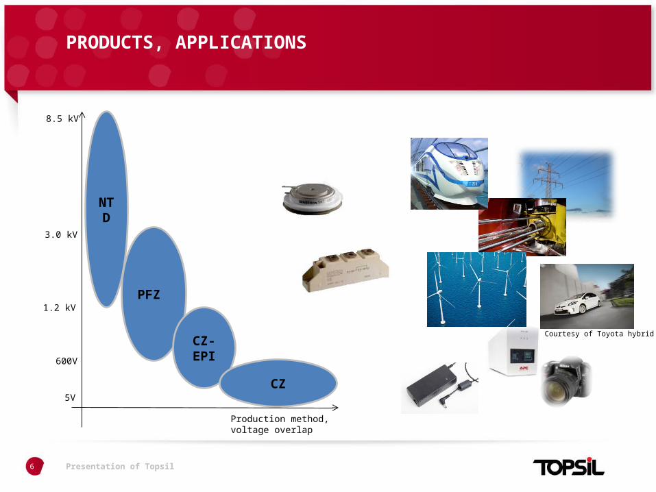
PRODUCTS, APPLICATIONS
NTD
PFZ
CZ-EPI
CZ
Production method, voltage overlap
5V
600V
1.2 kV
3.0 kV
8.5 kV
Courtesy of Toyota hybrid
Præsentation xx7 Presentation of Topsil
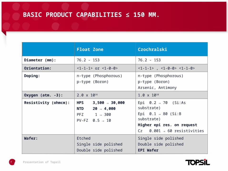
BASIC PRODUCT CAPABILITIES ≤ 150 MM.
Float Zone Czochralski
Diameter (mm): 76.2 - 153 76.2 - 153
Orientation: <1-1-1> or <1-0-0> <1-1-1> , <1-0-0> <1-1-0>
Doping: n-type (Phosphorous)p-type (Boron)
n-type (Phosphorous)p-type (Boron)Arsenic, Antimony
Oxygen (atm. -3): 2.0 x 10¹⁶ 1.0 x 10¹⁸
Resistivity (ohmcm): HPS 3,500 → 30,000NTD 20 → 4,000PFZ 1 → 300PV-FZ 0.5 → 10
Epi 0.2 → 70 (Si:As substrate)Epi 0.1 → 80 (Si:B substrate)Higher epi res. on requestCz 0.001 → 60 resistivities
Wafer: EtchedSingle side polishedDouble side polished
Single side polishedDouble side polishedEPI Wafer

Præsentation xx8 Presentation of Topsil
FZ 200 MM. PRODUCT CAPABILITIESPRODUCT KEY PARAMETERS
NTD PFZ High resistivity
material: HiRES®/HPS
Orientation: <1-0-0> <1-0-0> <1-0-0>
Doping: n-type (Phosphorous) n-type (Phosphorous)p-type (Boron)
n-type (Phosphorous)p-type (Boron)
Oxygenatoms/cm³
< 2.0 x 10¹⁶ < 2.0 x 10¹⁶ < 2.0 x 10¹⁶
Metals E10 atoms/cm²
< 2 < 2 < 2
Resistivity (ohmcm):
20 – 800 20 – 100 3.500 – 30.000
Resistivity Tolerance %
< 7% < 10% < 50% *
RRV% < 7% < 14% < 60% *
* Tolerances depending on resistivity target, test pattern and type

Præsentation xxPresentation of Topsil
Effect of nitrogen on the properties of Si single crystals
9
Præsentation xx10 Presentation of Topsil
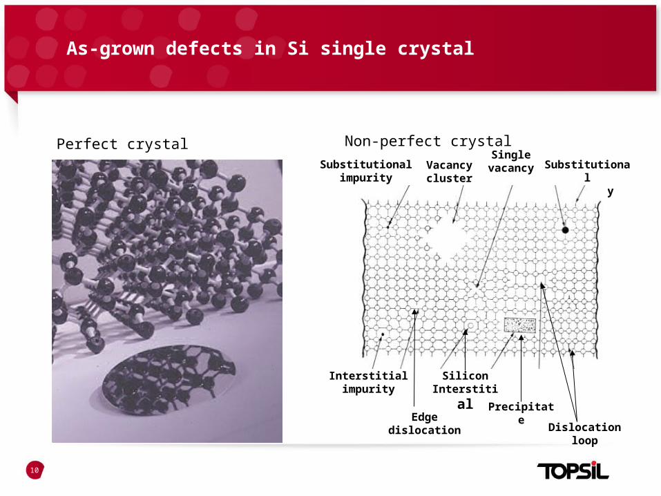
As-grown defects in Si single crystal
Perfect crystalSubstitutional
impurityVacancy cluster
Substitutionalimpurity
Non-perfect crystal
Interstitialimpurity
Edgedislocation
SiliconInterstitial
Precipitate
Dislocation loop
Single vacancy

Præsentation xx11 Presentation of Topsil
Nitrogen impact on microdefects
• V. Voronkov et al. Solid State Phenomena Vols. 131-133 (2008) pp 219-224
• Doping of silicon crystals with nitrogen has an effect on the
properties of grown-in microdefects
• In Si crystals vacancies are agglomerated into voids (the voids
are revealed by chemical etching as flow pattern effects)
• The void nucleation in FZ crystals occurs at temperature around
1000 oC
• The voids density is at 105 – 107 cm -3
• The void may include 103 - 105 vacancies
Præsentation xx12 Presentation of Topsil
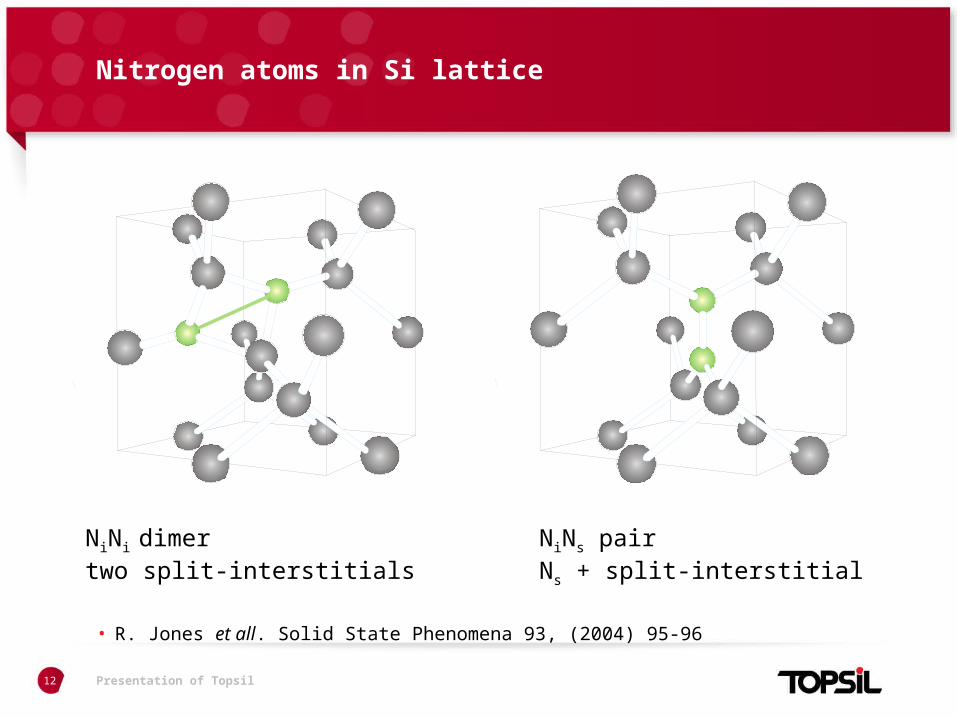
Nitrogen atoms in Si lattice
NiNs pairNs + split-interstitial
NiNi dimer
two split-interstitials
• R. Jones et all. Solid State Phenomena 93, (2004) 95-96
Præsentation xx13 Presentation of Topsil
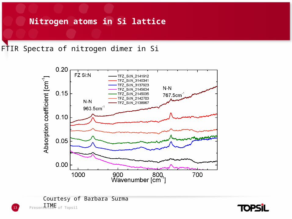
Nitrogen atoms in Si lattice
Courtesy of Barbara Surma ITME
FTIR Spectra of nitrogen dimer in Si

Præsentation xx14 Presentation of Topsil
Nitrogen atoms in Si lattice
The nitrogen concentration is determined from the height of the absorption peak at 963 cm-1 using the following calibration formula
[nitrogen concentration [at/cm-3] ] = 1.83 +/- 0.24 ) x 1017 x (absorption coefficient)
• Itoh Y et al. Appl. Phys. Lett. 47 (1995) 488-489
Courtesy of Barbara Surma ITME
Præsentation xx15 Presentation of Topsil
Nitrogen atoms in Si lattice
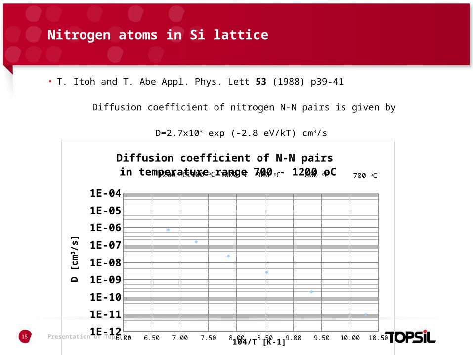
• T. Itoh and T. Abe Appl. Phys. Lett 53 (1988) p39-41
Diffusion coefficient of nitrogen N-N pairs is given by
D=2.7x10³ exp (-2.8 eV/kT) cm3/s
6.00 6.50 7.00 7.50 8.00 8.50 9.00 9.50 10.00 10.501E-12
1E-11
1E-10
1E-09
1E-08
1E-07
1E-06
1E-05
1E-04
Diffusion coefficient of N-N pairs in temperature range 700 - 1200 oC
104/T [K-1]
1200 oC 700 oC
D [c
m3 /
s]
800 oC900 oC1000 oC1100 oC
Præsentation xx16 Presentation of Topsil
Nitrogen atoms in Si lattice
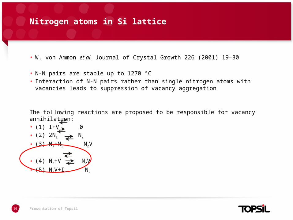
• W. von Ammon et al. Journal of Crystal Growth 226 (2001) 19–30
• N-N pairs are stable up to 1270 °C • Interaction of N-N pairs rather than single nitrogen atoms with vacancies leads to
suppression of vacancy aggregation
The following reactions are proposed to be responsible for vacancy annihilation: • (1) I+V 0• (2) 2Ni N2
• (3) Ns+Ni N2V
• (4) N2+V N2V
• (5) N2V+I N2
Præsentation xxPresentation of Topsil
• NitroSil project scope
17
Præsentation xx18 Presentation of Topsil
NitroSil
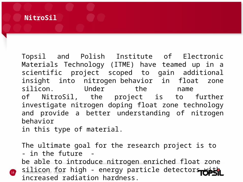
Topsil and Polish Institute of Electronic Materials Technology (ITME) have teamed up in a scientific project scoped to gain additional insight into nitrogen behavior in float zone silicon. Under the name of NitroSil, the project is to further investigate nitrogen doping float zone technology and provide a better understanding of nitrogen behavior in this type of material.
The ultimate goal for the research project is to - in the future - be able to introduce nitrogen enriched float zone silicon for high - energy particle detectors with increased radiation hardness.
Præsentation xxPresentation of Topsil
Topsil assignments
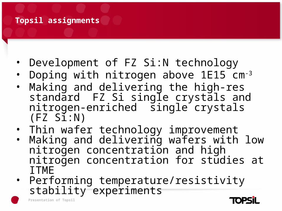
• Development of FZ Si:N technology • Doping with nitrogen above 1E15 cm-3 • Making and delivering the high-res standard FZ Si
single crystals and nitrogen-enriched single crystals (FZ Si:N)
• Thin wafer technology improvement• Making and delivering wafers with low nitrogen
concentration and high nitrogen concentration for studies at ITME
• Performing temperature/resistivity stability experiments

Præsentation xxPresentation of Topsil
ITME assignments with collaboration with KiT and CiS
• Determination of nitrogen, oxygen and carbon concentrations
• Proton irradiation and study of the radiation defect centers properties
• Fabrication, irradiation and studies of radiation defect centers in detector structures
• Standard FZ Si and FZ Si:N comparative studies

Præsentation xxPresentation of Topsil
Summary
21
Præsentation xx22 Presentation of Topsil
Summary and Conclusion
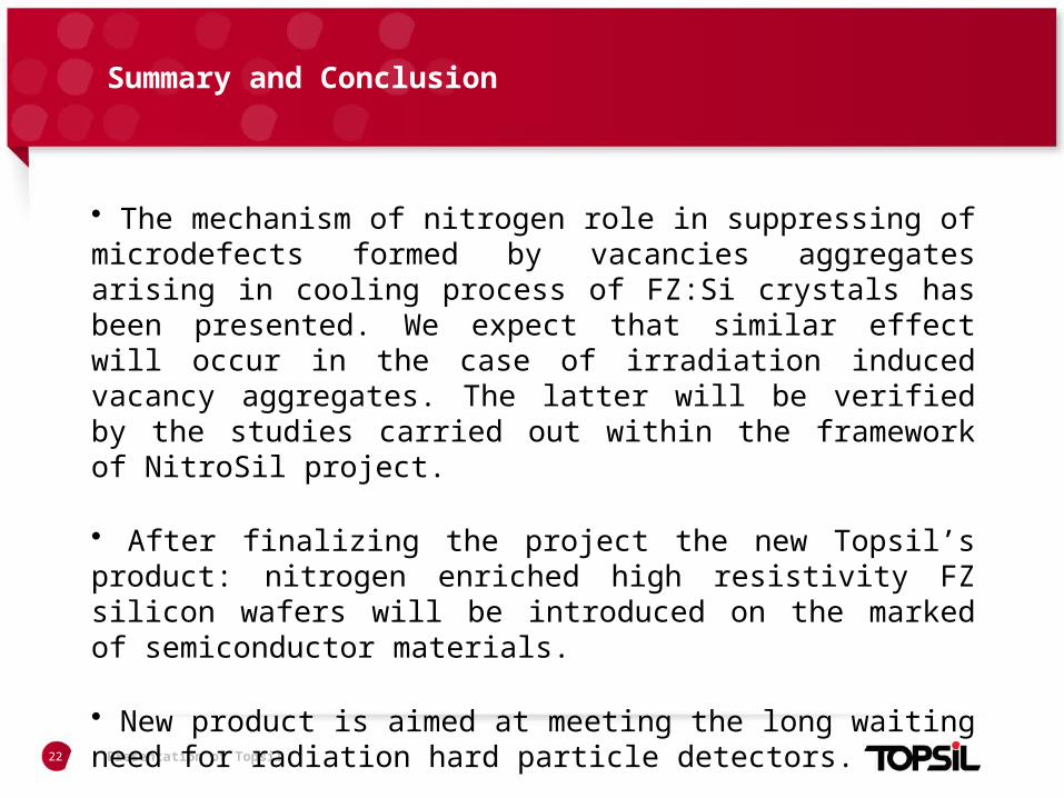
• The mechanism of nitrogen role in suppressing of microdefects formed by vacancies aggregates arising in cooling process of FZ:Si crystals has been presented. We expect that similar effect will occur in the case of irradiation induced vacancy aggregates. The latter will be verified by the studies carried out within the framework of NitroSil project.
• After finalizing the project the new Topsil’s product: nitrogen enriched high resistivity FZ silicon wafers will be introduced on the marked of semiconductor materials.
• New product is aimed at meeting the long waiting need for radiation hard particle detectors.
Præsentation xx23 Presentation of Topsil
Acknowledgements
This work has been partially supported by the Polish Centre for Research and Development within the framework of the NitroSil project (ID: 208346) financed by the Program for Applied Research (Contract No. PBS2 / A9 / 26/2014).
www.nitrosil.com
Thank you for your attention
Præsentation xx24 Presentation of Topsil
DISCLAIMER
This document has been prepared by Topsil Semiconductor Materials A/S. Unless stated in this document the following shall apply to the information.
The information, in particular the figures, data and schedules, are preliminary and for discussion purposes only. We do not represent that such information is true, accurate or complete and it should not be relied upon as such. No independent verification exercise has been undertaken in respect of the information.
All information, opinions and estimates in this document are Topsil Semiconductor Materials A/S judgment as at the date of this document and are subject to change without notice. While this information has been prepared in good faith, no representation or warranty, expressed or implied, is made.
The information in this document is supplied on the condition that Topsil Semiconductor Materials A/S, and any related party or employee of Topsil Semiconductor Materials A/S, are not liable for any error or inaccuracy, whether negligently caused or otherwise, or for any loss or damage suffered by any person due to such an error, omission or inaccuracy as a result of such supply.
Præsentation xx
THANK YOU
Topsil Semiconductor Materials A/SSiliciumvej 1DK-3600 Frederikssund, Denmark
MICHAEL KWESTARZNitroSil Project Coordinator
Phone: +48 22 835 19 39Fax: +48 22 865 77 35E-mail: [email protected]
Topsil Semiconductor Materials SA133 Wolczynska01 – 919 Warsaw, Poland