Embed Size (px)
Citation preview

6 V AN L-95/42
TechnologyTechnologyTechnologyTechnologyTechnologyTech no logy
DivisionDivisionDivisionDivisionDivisionDivision
Practical Superconductor
Development for ElectricalPower Applications
Annual Report for FY 1995
Argonie National Laboratory, Argonne. Illinois 60439operated by The University of Chicagofor the United States Department of Energy under Contract W-31-109-Eng-38
TSASTERGiSi if TICIN 'OF TWS (;i ,C rrIT S U",MtE !
EnergyEnergyEnergyEnergyEnergyEnergy
-

Argonne National Laboratory, with facilities in the states of Illinois and Idaho, isowned by the United States government, and operated by The University of Chicagounder the provisions of a contract with the Department of Energy.
DISCLAIMERThis report was prepared as an account of work sponsored by an agency ofthe United States Government. Neither the United States Government norany agency thereof, nor any of their employees, makes any warranty, expressor implied, or assumes any legal liability or responsibility for the accwacy,completeness, or usefulness of any information, aPparatus, product, or pro-cess disclosed, or represents that its use would not infi inge privately ownedrights. Reference herein to any specific commercial product, process, orservice by trade name, trademark, manufacturer, or otherwise, does notnecessarily constitute or imply its endorsement, recommendation, orfavoring by the United States Government or any agency thereof. The viewsand opinions of authors expressed herein do not necessarily state or reflectthose of the United States Government or any agency :hereof.
Reproduced from the best available copy.
Available to DOE and DOE contractors from theOffice of Scientific and Technical Information
P.O. Box 62Oak Ridge, TN 37831
Prices available from (423) 576-8401
Available to the public from theNational Technical Information Service
U.S. Department of CommerceI 5285 Port Royal Road
Springfield, VA 22161

Distribution Category:Electric Power
Applications (UC-1394)
ANL-95/ 42
ARGONNE NATIONAL LABORATORY9700 South Cass AvenueArgonne, Illinois 60439
PRACTICAL SUPERCONDUCTOR DEVELOPMENT FOR ELECTRICALPOWER APPLICATIONS
ANNUAL REPORT FOR FY 1995
U. Balachandran
Contributors:
T. R AskewY. S. ChaS. E. DorrisJ. T. DusekJ. E. EmersonB. L. FisherK. C. GorettaK. E. GraytJ. D. Hettingert
J. R. HullR. T. KampwirthtD. S. KuppermanM. T. LanaganJ. S. Luo t tM. MarinelliV. A. Maronit tR. L. McDanielN. Merchanttt
D. J. MillertR. C. NiemannJ. J. PiccioloT. PillaiJ. L. RoutbortJ. P. SinghV. R TodttK. L. UherkaC. A. Youngdahl
Energy Technology Division
October 1995
Work supported by
U.S. DEPARTMENT OF ENERGYOffice of Energy Efficiency and Renewable Energy
tMaterials Science Division.ttChemical Technology Division.

Contents
Abstract ............................................................................................................................................................. 1
1 Introduction........................................................................................................................................... 1
2 Technical Progress in 1994-1995 ............................................................................................... 2
2.1 Bi-Pb-Sr-Ca-Cu-O Superconductors............................................................................... 2
2.1.1 Phase Developm ent.................................................................................................. 2
2.1.2 Tape and Coil Developm ent.................................................................................. 12
2.2 Tl-M -Sr-Ba-Ca-Cu-O Superconductors ..................................................................... 35
2.2.1 Ag-Clad'I1-1223 Tapes and W ires..................................................................... 35
2.2.2 'l-Based Coatings and Film s................................................................................ 38
2.3 Y-Ba-Cu-O Superconductors................................................................................................ 45
2.3.1 M elt-Processed Y-123........................................................................................... 45
2.3.2 Grain Boundary Transport and Microstructure..................... 45
2.4 Properties of Bulk High-Ta Superconductors............................................................. 47
2.4.1 Characterization M ethods..................................................................................... 47
2.4.2 Electrical Characterization of Superconductors........................................... 47
2.4.3 Therm al Conductivity M easurem ents............................................................... 50
2.4.4 M echanical Properties......................................................................................... 51
2.4.5 Nondestructive Evaluation.....................................................................................52
2.5 Applications and Devices ...................................................................................................... 55
2.5.1 Current-Lead Projects............................................................................................. 56
2.5.2 Superconducting M agnetic Bearings ............................................................... 65
References.............................................................................................................................................. 69
iii

Figures
1 Critical current vs. Pb content for BI-2223 tapes heat treated at 8200Cin 8% 02 for total heat-treatment times of 50, 150, 250, and 350 hw ith interm ediate pressing........................................................................................................... 4
2 Backscattered electron images of Pbo.20, Pbo.30, Pbo.40, and Pbo.m,samples after 250 h at 820 C in 8%02............................................................................ 5
3 Correlation of Pb loss with Bi-2223 phase formation for fully sheathedand opened Ag/Bi-2223 composites heat treated at 8250C in 0.075 atm
02.............................................................................................................................................................. 7
4 Effect of Pb deployment in two-powder Ag/Bi-2223 composites oninduction period preceding initiation of BI-2223 formation reaction............. 8
5 Results of SEM/EDX analysis performed on samples from Dorris et al.(1993) Pb-deployment study, showing relative area fractions of second-phase material, unconverted Bi-2212, and Bi-2223............................................................9
6 Imaging Raman microscopy study of ceramic core of a fully processedAg/Bi-2223 composite, showing spatial distribution of Cu oxide,Ca2PIbO4, and Bi-2223 in typical core section......................................................................... 10
7 I values as a function of heat-treatment temperature for a series of
Ag/Bi-2223 composites with varying Pb and Sr content....................................................11
8 Critical current vs. length of 37-filament conductor at 77 K................... 13
9 Fractional conversion to BI-2223 vs. time for Ag/Bi-2223 compositeswith four filament counts, processed at 825-830*C in 0.075 atm 02............ 14
10 Schematic representation of apparatus used to coat Ag wire withBi-2223 precursor powder for use in CWIT process ......................................................... 15
11 Flow chart for CW IrT process.......................................................................................................... 16
12 Average critical current density Jc as a function of total heat-treatmentt iat815CIn8%k02.................................................................................. ......... 17
13 Transverse secondary electron image of CWIT #1, a coated-wire-in-tubesample heated for 50 h at 815*C in 8% 02.............................................................................19
14 Longitudinal secondary electron images of CWIT #1, a coated-wire-in-tube sample heated for 50 h at 815*C in 8% 02.................................................................20
15 Average critical current density Jc as a function of total heat-treatmenttime at 8150C in 8% 02 at 77 K and zero applied field ................................................... 21
iv
16 Normalized Ic vs. strain of mono- and multifilament conductors at 77 Kand 0.5 T applied magnetic field ................................................................................................ 22
17 Normalized Ic of mono- and multifilament conductor as a function ofbending radius..................................................................................................................................... 24
18 Normalized I vs. bending strain of monofilament conductors withthree superconductor fill factors................................................................................................24
19 Voltage lead placement in Ag/Bi-2223 specimen................................................................25
20 Line fit of voltage drop along Ag for sinter-forged Ag/Bi-2223,determined from model.................................................................................................................. 25
21 Calculated degradation of Je varying with crack density in Bi-2223 fortape at 77 K and 4.2 K...................................................................................................................... 27
22 Ic as function of heat-treatment time for butt joint and normal tape............... 27
23 SEM photomicrograph of butt joint after 250 h of heat treatment.............. 28
24 Dependence of Bi-2223 content on cooling rate of tapes sintered at825*C for 50 and 150 h ................................................................................................................... 28
25 Dependence of Je on cooling rate of tapes sintered at 825*C for 50 and150h........................................................................................................................................................ 28
26 SEM photomicrographs of Ag-sheathed Bi-2223 tapes sintered at825*C and cooled at 100, 50, 25, and 10*C/h........................................................................29
27 Improvement in phase purity with application of new heat-treatmentsch ed u le ................................................................................................................................................. 3 0
28 Back-scattered SEM photomicrograph of longitudinal cross section ofBi-2223 tape sintered according to improved schedule..................... 30
29 XRD data showing the evolution of Pb-2212 from freeze-driedprecursors ............................................................................................................................................. 32
30 DTA of tapes under various 02 partial pressures .................................................................. 32
31 Schematic representation of transverse cross section of an Ag-sheathedsuperconductor composite tape...................................................................................................32
32 Schematic representation of mechanical working of wires to producedifferent IPLs with identical cross- sectional area................................................................33
33 Critical current vs. IPL for unpressed tapes................................ 34
v

34 DTA data from calcined powders of TlI.l-XBiXBao.4Sr1.6Ca2Cu30X.................................. 36
35 SEM photomicrograph of calcined 11-1223 powder.......................................................... 36
36 XRD spectra for (T1,Bi)-1223 films annealed for zero time, 10, 20,and 30 min............................................................................................................................................ 40
37 Cross-sectional TEM photomicrographs of (T,Bi)-1223 films annealed
in Ag foil for10, 20, and 30 min............................................................................................... 41
38 XRD spectra for (T1,Bi)-1223 films annealed for 30 min and wrapped ineither Ag or Au foil............................................................................................................................. 42
39 Cross-sectional TEM photomicrograph of (T,Bi)-1223 films annealedin Au foil for 30 min.......................................................................................................................... 42
40 Je vs. magnetic field at various temperatures, before and after ionirradiation.............................................................................................................................................. 44
41 Electric field vs. current density of polycrystalline and epitaxialmaterials................................................................................................................................................. 44
42 Voltage vs. current for the samples in Fig. 41 before and afterirradiation.............................................................................................................................................. 44
43 TEM photomicrograph of 90* twist boundary in melt-processed Y-123.....................46
44 Multicontact fixture for differential AC voltage measurements at severalsites on superconductor bar.........................................................................................................48
45 Array of high-temperature superconductor bars prepared for AC power-bss tests at77K................................................................................................................................. 49
46 Thermal conductivity of Bi-2223................................................................................................52
47 Block diagram of acoustic microscopy setup for nondestructivecharacterization of Bi-2223 tapes................................................................................................ 53
48 Schematic diagram of ANL microfocus X-ray system........................................................... 54
49 Acoustic microscopy images ofBi-2223 tapes......................................................................55
50 Microfocus X-ray images of BI-2223 tapes ......................................... 56
51 Superconductivity, Inc., current lead prior to installation inperformance-evaluation cryostat ............................................................................................... 58
52 Burnout time prediction for Bi-2212 rod................................................................................58
vi

53 Babcock & Wilcox high-Ta superconductor: geometry of elements.............. 60
54 Babcock & Wilcox middle-stage current lead assembly.....................................................61
55 Babcock & Wilcox prototype safety lead assembly ............................................................... 61
56 Voltage drop vs. current at 60 K and B//c of a Babcock & Wilcoxconductor element............................................................................................................................. 62
57 Variation of retained Ic fraction with axial strain of Babcock & Wilcoxelement................................................................................................................................................... 62
58 Superconducting magnet and variable-temperature cryostat in ANLfacility for measuring Ic .................................................................................................................... 63
59 Voltage-vs.-current characteristics of ZerRes lead at various appliedfield s for T = 21 K ............................................................................................................................. 64
60 Voltage-vs.-current characteristics of ZerRes lead at various appliedfields for T = 59 K.............................................................................................................................. 64
61 Voltage-vs.-current characteristics at various applied fields for atemperature gradient of 20-60 K across the lead................................................................65
62 Voltage-vs.-current characteristics of ZerRes lead at varioustemperatures for zero applied field ........................................................................................... 65
63 Rotor A and FTA vacuum test chamber...................................................................................... 66
64 Friction coefficient for Rotor B permanent magnet as a function oflevitation gap height.......................................................................................................................... 68
Tables
1 Stoichiometry of Bi-2223 precursor powders as determined byIC P -A E S .................................................................................................................................................... 3
2 Summary of melting behavior of T1 1.1-xBixBao.4Sr1.6Ca2Cu3Ox................... 37
vii

PRACTICAL SUPERCONDUCTOR DEVELOPMENT FOR ELECTRICALPOWER APPLICATIONS
ANNUAL REPORT FOR FY 1995
Abstract
Development of useful high-critical-temperature (high-Ta) superconductors requiressynthesis of superconducting compounds; fabrication of wires, tapes, and films from thesecompounds; production of composite structures that incorporate stabilizers or insulators;and design and testing of efficient components. This report describes the technicalprogress of research and development efforts aimed at producing superconductingcomponents in the (Bi,Pb)-Sr-Ca-Cu, (T,Pb,Bi,V)- (Ba,Sr)-Ca-Cu, and Y-Ba-Cu oxidesystems. The topics that are discussed are synthesis and heat treatment of high-Tesuperconductors, formation of monolithic and composite conductors, characterization of
structures and superconducting and mechanical properties, and fabrication and testing of
prototype components. Collaboration with industry and academia is documented.
1 Introduction
The superconductor program at Argonne National Laboratory (ANL) includes develop-ment of buik and film processing that is directed toward improving the properties ofhigh-critical-temperature (high-Tc) superconductors, developing processing methods forthe production of commercial conductors, and fabricating and testing prototype conduc-tors. Team relationships with industrial and academic partners are an integral part of thisprogram. The principal objective of the ANL program is to develop methods to fabricate
and use structurally reliable high-Te superconductors for the generation, transmission,and storage of electrical energy. Ceramic processing and joining techniques are beingdeveloped to provide useful conductors from one or several high-Ta superconductors.Work has focused on superconductors based on bismuth-strontium-calcium-copper oxide
(Bi-2212), lead-doped bismuth-strontium-calcium-copper oxide (Bi-2223), and pure andmetal-doped (M, where M is bismuth, lead, or vanadium) thallium-strontium-barium-
calcium-copper oxide (T1-1223), and yttrium-barium-copper oxide (Y-123).
Monolithic and composite conductors in the form of wires, tapes, films, or othershapes must meet several requirements. For most applications, the conductors must becapable of carrying large currents in the presence of large magnetic fields and they mustbe strong, flexible, and chemically and cryogenically stable. Potential applications for suchconductors include transmission lines, motors, generators, transformers, magnetic energystorage devices, and electronics. The principal impediments to the use of bulk high-Tasuperconductors are low critical current density (Jo) in large applied magnetic fields,relatively poor mechanical properties, and the need for very long lengths with uniformproperties. Processing methods for improveing all of the characteristics of high-Tasuperconductors have been and continue to be developed. The goals of ceramic fabricationinclude promoting high conductivity by obtaining phase-pure final materials dnd impartingfavorable grain alignment, which will maximize flux pinning through microstructuralcontrol, and increasing flexibility and reliability by minimizing microstructural flaws and
optimizing the strength and toughness of each material.

-2-
This report reviews the technical progress and status of (1) Bi- and T1-based high-Tcsuperconductor wires and tapes, wnich constitute the main focus of the materials efforts;(2) Y- 123 superconductors; (3) characterization of superconducting and electrical prop-erties, microstructures, and mechanical properties; (4) investigation of fundamental prop-erties; and (5) fabrication and testing of prototype superconducting devices. Interactionwith industry and academia is also documented.
2 Technical Progress in 1994-1995
2.1 BI-Pb-Sr-Ca-Cu-O Superconductors
2.1.1 Phase Development
Composition Studies
The effect of total Pb content on the microstructure and Jc of Bi-2223 tapes that weremade by the two-powder process was investigated. Earlier studies suggested what seemedsuperficially to be contradicting trends (Balachandran et al., 1994a; Dorris et al., 1993,1994a). One study indicated that phase purity improved and Jc increased as Pb contentincreased from Pbo.3 to Pbo. 4; a second study showed that Je decreased as the Pb contentincreased from Pbo.3 to Pbo.5 because of the appearance of a Pb/Bi-rich phase in thesamples that contained more Pb. The difference was attributed to variations in composi-tion other than Pb content (the Sr content of the first Pbo.3 sample was relatively high andthe (Bi+Pb) content was relatively low when compared with later Pbo.3 samples). Bothstudies showed that an optimum Pb content exists and that deviations of Pbo. 1 from theoptimum strongly influence the microstructure and properties of tapes. It was proposedthat Bi-2223 formation is retarded and Jc is decreased when the Pb content is too low,because the necessary liquid phase does not form, whereas Je decreases when the Pbcontent is too high because Pb/Bi-rich phases coat the grain boundaries. To confirm theseideas and to better optimize the Pb content, powder-in-tube (PIT) tapes were made frompowders with Pb content between Pbo.3 and Pb0 .5.
Pb-doped Bi-2212 powders, Bil.SPbXSr2.oCal.oCu2O8, were prepared for x values of0.20, 0.25, 0.30, 0.35, 0.40, and 0.50. Powder mixtures with appropriate amounts ofBi2O3 , PbO, SrCO3, CaCO3, and CuO were first calcined at reduced total pressure of Q3 torr02 (20*C/h to 750*C, followed by 6 h at 750*C) to ensure complete decomposition of thecarbonates. After calcining at reduced pressure, the Bi-2212 phase was formed by furthercalcining for 24 h at 840*C in C02-free air at ambient pressure. The powders were ballmilled in isopropyl alcohol for 12-16 h and calcined again for 24 h at 840*C in C02-free airat ambient pressure. Calcinations in ambient air were repeated with intermediate ballmilling until nearly single-phase materials were obtained. The powders were thencalcined at reduced total pressure to rid the powders of Ca2PbO4 and ensure that all Pb wascontained in the BI-2212 phase (Jeremie et al., 1993). Powders of 2223 precursor wereprepared by mixing each of the Bi-2212 powders with an equimolar amount of CaCuO2,then ball milling in isopropyl alcohol for 12-16 h and calcining at =3 torr (60*C/h to 720*C,followed by 3 h at 720*C) to eliminate C introduced by milling. PIT tapes were preparedfrom the Bi-2223 precursor powders by an established procedure (Dorris et al., 1993a).
Samples ("3 cm long) were cut from the tapes and heat treated in 8% 02 at temper-atures of 820 and 8270C. Thermomechanical processing of the tapes began with a 50-hannealing at the chosen heat-treatment temperature, after which the tapes were uniaxially
-3-
cold pressed at =2 GPa. Following pressing, the tapes were annealed for an additional100 h at the selected heat-treatment temperature. The process of pressing and thenannealing was repeated until cumulative heat-treatment times of 350 h had been reached.The Jc of each tape was measured at 77 K in zero applied field with a 1 V/cm criterionand the four-probe method. Each reported Je value represents the average of measure-ments made on three separate samples. The degree of conversion to Bi-2223 wasestimated by X-ray analysis of peeled tapes. The Bi-2223 fraction was calculated asIcj-i(2223)/[Ioo-10(2223)+1008(2212)1, where I-1io(2 2 2 3 ) and 1008(2212) are theintegrated peak intensities for the (00-10) reflection of 2223 and (008) reflection ofBi-2212, respectively.
X-ray analysis showed that the Bi-2212 powders had nearly identical phase purities,containing mostly Bi-2212, no Ca2PbO 4 , and only a slight amount of Bi-2201. The carboncontent of all Bi-2223 precursor powders was ~500 ppm or less. Analysis of the Bi-2223precursor powders by inductively coupled plasma-atomic emission spectroscopy (ICP-AES)produced the results shown in Table 1. Ic (0 T, 77 K) data for tapes that were heat treatedat 827'*C are shown in Fig. 1. The thickness of the tapes was typically 100-120 sm andtheir cross-sectional area was typically =2.0 x 10⁻³ cm2 .
Table 1. Stoichiometry of Bi-2223 precursor powders as determined by ICP-AES
Nominal Composition Bi Pb Sr Ca 01
Bil.8Pbo.20Sr2.oCa2.oCu3.oOlo 1.82 0.20 1.98 1.95 3.05
Bil.8Pbo.25Sr2.0)Ca 2 .oCu 3 .oO o 1.81 0.25 1.97 1.97 3.06
Bil.8Pbo.30Sr2.oCa2.oCu3.0010 1.80 0.29 1.96 1.98 3.07Bi1. 8 Pbo.3 5Sr2.oCa2 .oCu3 .o) 0 1.80 0.35 1.98 1.96 3.07
Bil.8Pbo.4oSr2.oCa2.oCu3.oO10 1.77 0.39 1.98 1.97 3.09Bil.8Pbo.5oSr2.oCa2.oCu3.oOlo 1.79 0.49 1.97 1.96 3.09
The Ic (0 T, 77 K) data shown in Fig. 1 clearly show that the optimum Pb content is=Pbo.3 for the composition studied -"e. Samples heated at 820*C showed the same trendwith Pb content, but their Ic values .ere =10% lower. As suggested earlier, the optimumPb content depends on the concentrations of the other constituents, so the optimum Pbcontent may differ for another composition. Figure 2 shows backscattered electron imagesof tapes (longitudinal view) after 250 h at 820*C in 8% 02. The Pbo.2o sample (Fig. 2a)contained primarily 2:1 alkaline earth cuprate, CuO, and Bi-2212, the phases that wereinitially present in the precursor mixture, suggesting that the formation of Bi-2223 wasslow. The Pbo.3 sample (Fig. 2b) contained the same second phases but in smaller con-centrations. X-ray analysis of peeled tapes showed that the Pbo.2 sample contained only=60% Bi-2223 after 250 h of heat treatment, whereas the Pbo.3 sample consisted of =98%Bi-2223 (the small amount of Bi-2223 in the Pbo.2 is believed to form during coolingbecause of back reaction). These results are consistent with idea that Bi-2223 formation isretarded when Pb content is too low, presumably because of the absence of a liquid phase.

-4-
40
35
30
25
20
15
10
5
0
0.15 0.2 0.25 0.3 0.35 0.4 0.45 0.5 0.55
Pb Content
FIg. 1. Critical current (I) vs. Pb content for Bi-2223 tapes heat treatedat 820*C in 8% 02 for total heat-treatment times of 50, 150,250, and 350 h with intermediate pressing.
The density of the Pbo,4 sample (Fig. 2c) was higher than that of the PbO.3 sample,hinting that Pbo.4 may have contained more liquid during the reaction. However, theconcentration of alkaline-earth cuprates and CuO was approximately the same for the twosamples, suggesting that the degree of Bi-2223 conversion was similar . These findingswere confirmed by X-ray analysis, which showed that both samples contained 95-98%BI-2223 after 250 h at 820*C. In addition to the alkaline earth cuprates and CuO,however, thin streaks of a Bi/Pb-rich phase were evident in the Pbo.4 sample. Thesestreaks can be seen in the Pb0.4 sample only at higher magnification, but are obvious in thePbo.5 sample (Fig. 2d), where they are larger and more abundant. The appearance of theBi/Pb-rich phase suggests that the Pb content of Pbo.4 was too high. The increase in Pbcontent evidently increases the core density but degrades the phase purity, and, as a resultcauses Ic to decrease.
This study confirms Pb content as a critical variable in fabricating tapes by the two-powder process and that deviations of Pbo.1 from the optimum strongly influence themicrostructure and properties of these tapes. When the Pb content is lower thanoptimum, Bi-2223 formation is retarded, presumably because a liquid phase is lacking,whereas a Bi/Pb-rich phase forms when the Pb content is higher than optimum. Theseresults indicate that the optimum Pb content depends on the content of the other Bi-2223constituents. For example, Maewski et al. (1991) indicate that a liquid phase does notform in samples with a high alkaline-earth concentration or a low (Bi+Pb) content. so, forsuch samples, the optimum may be expected to shift to higher Pb content.
-0--- 50 hr
-0----- 150 hr
- - 250 hr
-v-- 350 hr
0 T
-5-
Fig. 2. Backscattered electron images of (a) Pbo.20, (b) Pbo.3 0, (c) Pbo.4 0, and (d) Pbo.5 0samples (longitudinal views) after 250 h at 820 C in 8% 02.
Microstructural Development in Ag/Bi-2223 Conductors: Role of Lead
The purpose of this ongoing project is to investigate the evaluation of Bi(Pb)-Sr-Ca-Cu-O phase with respect to microstructural development during thermomechanicalprocessing of Ag/Bi-2223 composite conductors (De Rochemont et al., 1994). A majorobjective during FY 1995 has been to elucidate/characterize the role that Pb plays in theformation of Bi-2223 during heat treatment. The intention of this objective is to identifythe optimum Pb stoichiometry and Pb incorporation method for maximum compositeconductor performance, primarily in terms of Jc at 77 K.
In FY 1995, we conducted detailed followup work on specimens and results from theprior year's work (Dorris et al., 1994a and b; Tetenbaum et al., 1994, 1995) which showedthat incorporation of most of the Pb into the Bi-2212 component of the precursor powderproduced Ag/Bi-2223 composites with higher Je values than did incorporation of the leadas Ca 2 PbO4 in the second-phase component of the precursor powder. In the course of thiswork, we found that Pb loss during heat treatment of Ag/Bi-2223 composite conductorsblocks the progress of Bi-2223 formation; the mode of Pb incorporation is the major factorthat controls the length of the induction period preceding the onset of Bi-2223 formation;
-6-
fully' processed composites that are fabricated from powders with Pb in the BI-2212 com-ponent had fewer Bi-2212 intergrowths and back-reacted grains than did compositesmade from powders with Pb in the Ca2PbO4 form: a reaction that involves Pb transportationbetween orthorhombic Bi(Pb)-2212 and tetragonal Bi-2212 + Ca2 PbO4 can be manipulatedby adjusting 02 pressure and processing temperature and this reaction can be probed bothchemically and spatially by imaging Raman microscopy; and the Pb stoichiometry of theprecursor powder is connected in a sensitive way to the development of BI-2223 phase, tothe microstructure of the composite core, and to the Jc of the composite conductor.The key features of these results are summarized below.
Previously, we reported the results of a study designed to explore the effectiveness ofthe Ag sheath in limiting Pb loss during heat treatment of Ag/Bi-2223 composites (Poeppelet al., 1993). Additional measurements to quantify the Pb loss rate under the conditions ofour prior study have now been completed and are reported in Fig. 3, together with theFY 1993 phase conversion results and some additional conversion data collected during thepast year. In the quantification experiments, short sections (=25 mm in length) of Ag/Bi-2223 composites were peeled open prior to heat treatment to expose the ceramic core.These opened samples were processed at 825'C in 0.075 atm 02 for various times rangingfrom 10 to =30,000 min and then analyzed for Pb loss by ICP-AES. Fully sheathedspecimens of the same composite were run in parallel with the opened specimens toprovide a baseline for determining both the phase conversion kinetics and the level ofcontainment provided by the sheath.
The results in Fig. 3 show that the closed (fully sheathed) composite specimensreached complete conversion to Bi-2223 in =2000 min, whereas the open specimensnever achieved more than =40% conversion (as reported in our prior work). The Pb loss(presumably due to evaporation) is relatively small (a few percent) for the closed speci-mens and probably occurs by seeping out of the ends of the short samples. Lead loss fromthe opened specimens is continuous and nearly complete after =3 x 10⁴ min (=500 h).Also, after =1000 min, half of the Pb is lost from the opened samples and the Bi-2223formation reaction stops. Two conclusions can be drawn from these results: (1) Pb isessential to the conversion reaction and (2) the Ag sheath plays a key role in retaining thePb during heat treatment. The Bi-2223 that forms prior to =50% Pb loss does not tend todecompose as the remaining Pb vaporizes out of the sample. This latter observationsuggests that Pb is more centrally involved in the conversion reaction than it is instabilizing the Bi-2223 phase.
Figure 4 presents the results of a series of experiments designed to explore the earlystages (first 1000 min) of the thermomechanical process for two-powder Ag/Bi-2223composites. In this work, Bi-2223 precursor powders were formed by mixingB1 2 PbzSr2 CaCu2 0X with a Pb(o.4-)-Ca-Cu-0 second phase. Fully processed samples with aseries of z values produced the Je values presented in the upper curve in Fig. 4. DuringFY 1995, as-rolled specimens from this same series of composites were heat treated for10, 100, 300, and 1000 min, then quenched and analyzed by X-ray diffraction (XRD) forphase conversion to Bi-2223. After 10 min, there was no evidence of Bi-2223 for any ofthe z values; after 100 min, only the z = 0.3 sample showed the presence of Bi-2223; andafter 300 min, samples from z = 0.2 to z = 0.4 had reacted to form Bi-2223. After 1000min, all of the samples showed signs of reaction, but the samples with higher z values (i.e.,with half or more of the Pb in the Bi-2212 component of the precursor) had progressed

-7-
0.5
100 ,,----- -- e--
90" 0.4
.. 80
70 Pb Content Conversion -
N 60 As-rolled As-rolled 0.3.OpenOpened
50
c 40 'f- ---- '----- -- "- 0.2V
0 1030 ,. +
O 20
100
0 ---------- 2-'
0
10 102 103 104 105
Time (min)
Fig. 3. Correlation of Pb loss with Bi-2223 phase formation for fully sheathed (as-rolled)
and opened Ag/Bi-2223 composites heat treated at 825'C in 0.075 am 02
significantly farther in terms of Bi-2223 formation. From these experiments, we find that
the mode of lead deployment profoundly influencess the induction period preceding the
onset of Bi-2223 formation in two-powder Ag/Bi-2223 composites.
Figure 5 contains a summary of extensive scanning electron microscopy (SEM) and
energy-dispersive X-ray (EDX) examination of fully processed samples; the Je curve for this
series of composite specimens is again reproduced in this figure. SEM/EDX findings with
regard to second phase (mainly alkaline-earth cuprates), Bi-2212, and Bi-2223 fractions
indicate that all of the samples in the series contain 5-30% of second-phase material,
including the z = 0.4 sample that produced the highest Jc. The most significant correla-
tion with Je is the amount of residual Bi-2212, which is lowest for the samples with the
highest Jc. Furthermore, from the character of the Bi-2212 grains detected by SEM/EDX
it appears that they may have formed in part as a result of BI-2223 decomposition during
the ramped cooldown period following the final heat treatment. This back reaction may be
facilitated by residual liquid phase that persists (even after 250 h of heat treatment) for
some z values because the Pb that causes the formation of this liquid phase is not yet fully
deployed in Bi-2223 grains, i.e., the formation reaction in most of the samples was not
complete at the end of the final heat treatment.
The addition of Pb to the Bi-2212 phase is known to cause a crystallographic trans-
formation from a tetragonal (T) structure (Pb-free) to an orthorhombic (0) structure (Pb-
doped). There is mounting evidence that during the Bi-2223 formation reaction, Pb first
enters the Bi-2212 phase effecting this T -+ 0 transformation and then Bi-2223 grains
grow by liquid phase transport of alkaline-earth cuprates to the Pb-doped Bi-2212. We
have successfully utilized Raman microspectroscopy (RMS) and imaging Raman microscopy

-8-
75 22
70-- -> 20
65
60 18
55 I 1I ~ 16
50
M 45 e' 1,000 min14 1
40~40 12
35 0CS
1030 0.
025 I 820) I
2,'30Qmin
15
10 do .le 4
1001min
. 2
0 - -" "" "-----
10 min
I I I 0
0 0.1 0.2 0.3 0.4
Z
Fig. 4. Effect of Pb deployment in two-powder Ag/Bi-2223 com-posites on induction period preceding initiation of Bi-2223 formation reaction (10, 100, 300, and 1000 min),where z is stoichiometric Pb content of the Bi-2212component. Solid-line curve shows Je for fully processedconductor as reported by Dorris et al. (1993).
(IRM) to explore the T -+ 0 transition and to identify and image Pb-containing phases inBI-2223 pellets and Ag-clad composites. Specifically, we have observed a Pb-rich phasesurrounding T BI-2212 crystals that had been formed by controlled back reaction ofPb-doped 0 BI-2212.
The general procedure for applying RMS and !RM on Ag/Bi-2223 composites isdepicted in Fig. 6. The defocused Raman spectrum of the circled region in the white lightimage contains significant features at (A) 298, (B) 543, and (C) 632 cm-1. IRM images ofpeaks A, B, and C, ratioed against the adjacent average background (designated A/B1, B/B2,and C/B2, respectively, where B1 and B2 are the average backgrounds defined in Fig. 4)show the location of the species that generate each peak. Focused RMS scans, taken atpoints X, Y, and Z in the white-light image, produced the spectra labeled as Focused X, Y,and Z in Fig. 6. Comparison of these spectra with Raman spectra of standard materialsleaves no doubt that Image A/B1 is that of a Cu oxide particle (which appears in the centerof the white-light image), Image B/B2 shows the location of several Ca2 PbO4 particles, and

-9-
1
0.9
0.8
0.7
0.60U
i 0.5(U
0.4
0.3
0.2
0.1
0
Remainder above barspresumed representative offraction of Bi-2223 phase
0 0.1 0.2 0.3 0.4
z, Amount of Pb In BI-2212
Fig. 5. Results of SEM/EDX analysis performed onsamples from Dorris et al. (1993) Pb-deployment study, showing relative areafractions of second-phase material,unconverted Bi-2212, and Bi-2223.
Image C/B2 shows where Bi-2223 is located in the white-light image. RMS/IRM studieslike this one are providing new insights into spatial distributions of key phases thatparticipate in the Bi-2223 formation reaction.
In light of the growing body of evidence that Pb significantly influences phase evolutionand microstructure development during thermomechanical processing of Ag/Bi-2223composites (Luo et al., 1994a and b; Merchant et al., 1994a and b), we initiated a study toexplore the effects of perturbations of metal atom stoichiometry on Ic in Ag/Bi-2223composite conductors. In the first study of this series, we tested the effect of varying Pbstoichiometry over the range of 0.3-0.5 for two Sr values (1.9 and 2.0), using a fixed set ofBi (1.72 0.05), Ca (1.97 0.01), and Cu (3.10 0.02) stoichiometries. The results of thistest are shown in Fig. 7. An optimum was achieved for Pb = 0.3, with seemingly littlesensitivity to the Sr value. Future tests in this series will include Pb values <0.3, as well asvariations of Bi, Ca, and Cu stoichiometries.
A
- Second phase
Bi-2212
isJ
25
20
15
E
1
10
5
0
4500 DefocusedA (29) ;C(632)
4000 - -B(543); ----
3500 --- -- --- ---
3000 -- - - ------
2500 - -L---- --- ---
20M ------ ----- ---
BG2 BG31500 328):-503)T-- ---
BG41000 -..-....--- (690).-BG1 (60
500 26 ) --------------4276-xA
0200 400 600 800
Wavenumbers
White Light
-
500
3000
2500
2000
1500
1000
500
Focused X
-- - -------
- - -- . - --
1..aoo
10000
B000
6000
4000
2000
0200 400 600 800
Wavenumbers
ABi
Focused V
- -- ----.
Ca2Pb.40 I
200 400 600 8
Wavenumbers
BIB2
00
Focused Z5000
45 0 - -
4000 ----- -- -- ----
3500 ---- - -- -----
3000 - -'--------'---
2500 --
2000 - ----- -- --------- --
1500 ------ ------- -
1000 -
500 ----------------------Bi-2223
a I I200 400 600 600
Wavenumbers
CIB2
10ism B1 = (BG1+BG2)/2 B2 = (BG3+BG4)/2
FIg. 6. Imaging Raman microscopy study of ceramic core of a fully processed Ag/Bi-2223 composite, showing spatialdistribution of Cu oxide, Ca2PbO4 , and Bi-2223 in typical core section.
00
Y-X-

-11-
40 . , , , , , , , , , ,
35 E.(r ) , ''* Pb=0.30
30,'Fig. 7.Ic values as a function of heat-
25 treatment temperature for a series20 - of Ag/Bi-2223 composites with
15 varying Pb and Sr content Fixed
10- . ... Pb = 0.40 stoichiometries were maintained1" _- . --- a Pb =0.45 for Bi (1.72 0.05), Ca (1.97 t
5 - .: -'Pb0.50 0.01), and Cu (3.10 0.02); pro-0 ___________________ cessing sequence between rolls
810 815 V20 825 830 835 was 50/100/100 h in 0.08 atm.02 .
Temperature (C)
50
(Sr2 0 )40 A
30I Pb= 0.30
20
-+ Pb = 0.40
10 -z' -Pb=0.45..------- " ---- "---- Pb =0.50
0
810 815 820 825 830 835
Temperature (C)
Collaborative Phase-Development Work with American Superconductor Corporation
A significant portion of the work on Pb effects was conducted in collaboration withAmerican Superconductor Corporation (ASC) and the ASC-led Wire Development Group(WDG). Although the composite conductors employed to produce the above-reportedresults were fabricated at ANL, several key experimental powders and pressed pellets thatwere examined at ANL were synthesized at ASC and at Los Alamos National Laboratory.The insights gained from this work have been shared with ASC and the other members ofthe WDG in connection with their in-house powder processing and composite fabricationactivities and their contributions to the advances in Ag/Bi-2223 conductor performanceachieved by ASC during FY 1995.
Collaboration with Ames Laboratory/Iowa State University
Despite considerable success in the development of commercial processes for prepa-ration of Bi-2223, many details of the chemistry that occurs at high temperature are notwell understood. For a standard PIT process, growth of Bi-2223 is usually carried outinside an Ag sheath and can typially be completed in a few days. The optimal propertiesoften depend on the phases in the starting materials, the partial pressure of 02, the prox-imity of Ag, and a host of other processing variables. One way to observe the phases that

-12-
form during processing is to quench at intermediate times and look for phases in thequenched material. A complementary method is to study the transformation in situ withX-rays (Polonka et al., 1993). The quench method has the advantage of reproducing theconditions of the commercial process better than the X-ray method, but it is not certainthat all phases are preserved during the quench. The X-ray method has the advantage ofdirect observation of the process. The disadvantage is that the X-rays penetrate only
1 m, so only the surface grains are observed. Hence, the two methods are complemen-tary. Our goal is to determine the identity of the phases that form during the transfor-mation, the kinetics of growth and decay of various phases, and the changes in kineticswith temperature.
We have used in-situ high-temperature X-ray measurements to follow the crystallo-graphic changes that occur as Pb-doped BI-2212 plus other phases transform into Bi-2223in a PIT process for forming tape conductors. On the initial ramp to the reaction temper-ature, the Bi-2212 X-ray Lines first diminish in amplitude and then begin to grow againabove 700*C. Significant changes occur at 790*C. Lines associated with Ca2PbO4 form, butthen disappear after 20-230 min at temperature. The Bi-2223 phase begins to grow at-810*C (Xu et al., 1995a and b).
2.1.2 Tape and Coil Development
Several programs in wire, tape, and coil development are ongoing. Much of the effortis focused on direct collaboration with industry. Each effort will be discussed individually.
Collaboration with Intermagnetics General Corporation
For the past few years, we have collaborated with Intermagnetics General Corporation(IGC) to develop high-Ta superconducting wires and tapes for possible electric power andhigh-field magnet applications. Potential commercial applications of the conductorsinclude motors, generators, and transmission cables. Fabricating robust and high-qualityconductors is important for the various applications envisaged for high-Tc superconductors.
The Ag-clad Bi-2223 conductors were fabricated by the PIT technique whereinpartially reacted Bi-2223 powders were packed into high-purity Ag tubes, drawn through aseries of dies and then rolled to a final thickness of =0.1 mm. Through a series of uniaxial-pressing and heat treatments, a Je value >4 x 10⁴ A/cm2 has been obtained in short-lengthsamples (Balachandran et al., 1994b). Because uniaxial pressing is not suitable for fabri-cating long-length conductors, a modified processing technique was employed for fabri-cating monocore and multifilament conductors (Haldar et al., 1994).
At 77 K and zero applied field, a Je of =1.6 x 10⁴ A/cm2 has been achieved in a 125-mmonofilament conductor. Figure 8 shows the Ic along the length of an 850-m 37-filamentconductor. The Ic was 16 A, corresponding to a Je of 1.2 x 10⁴ A/cm2 . Recently, a 1250-m37-filament conductor was fabricated with an overall J >1 x 10⁴ A/cm2. Consistent resultshave been obtained from long-length monocore and multifilament conductors, indicatingthat considerable progress has been made in their development. Compact and robustpancake coils have been fabricated from these conductors. The coils and test magnetshave been characterized at various temperatures and applied magnetic fields. A testmagnet, fabricated with eight double pancake coils, generated a field of 1 T at 4.2 K and0.6 T at 27 K. in a background field of 20 T. Total length of the conductor in the magnetwas 770 m.

-13-
30
25 Fig. 8.
20 Critical current vs. length-0 " of 37-filament conductor at
r15.0i077 K.
10
0 200 400 600 800 1000
Length (n)
American Superconductor Corporation Collaboration
Our collaborative fabrication project with ASC, which includes ANL participation in theASC-led WDG, has continued during FY 1995. The primary emphasis of the ANL contri-bution has been on phase evolution and microstructure development in Ag/Bi-2223multifilament composite conductors. In this activity we are exploring the influence/effectof key processing parameters (i.e., temperature, 02 pressure, and time) by applying thesame methodology that was developed earlier for monofilaments. An added feature of thework on multifilament composites relates to the filament count and its possible influenceon the Bi-2223 formation reaction. Figure 9 shows conversion-vs. -time data for fourcomposites with a wide range of filament counts. (The composites designated OPIT werefabricated from oxide powder precursors, whereas the one designated MP contained ametallic precursor powder.) Within the limits of the characteristic uncertainty for thesetypes of measurements, the filament count does not seem to discernibly influence thekinetics of Bi-2223 formation. Related studies of 02 pressure and temperature variationsindicate that Ag/Bi-2223 multifilament composites behave in a manner similar to thatwhich was observed for Ag/Bi-2223 monofilaments in prior years.
Wire-in-Tube Processing
A coated-wire-in-tube (CWIT) process for fabricating Ag/superconductor compositeconductors is being developed in collaboration with BASF Corp. This process has severalpotential advantages, the most important of which is that it greatly increases theAg/superconductor interface area. This may significantly enhance superconductingproperties, because abundant evidence exists (Lelovic et al., 1995a; Pashitski et al., 1995;Welp et al., 1995) that a thin, well-aligned layer at the Ag/superconductor interface carriesa large fraction of the current in Ag-sheathed conductors. Also, the matrix of CWITconductors consists of superconductor, whereas Ag forms the matrix of multifilamentconductors, another type of conductor with an increased Ag/superconductor interface area.As a result, percolation through CWIT conductors may be improved relative to multifil-ament conductors, where small-scale disruptions, such as second-phase particles orcracks, may force transport through the Ag. In addition, the thickness of superconductor

-14-
1.2" OPIT Monofilament
1 0 OPIT 19 filaments -
o OPIT 85 filaments X
0.8 - x MP 361 filamentsN "
m 0.6
0 0.4.;X 2 "
0.2 -
0 eo-
-0-.2 -- - - - ---- - -- --- -
10 100 1000 104Time (mm)
Fig. 9. Fractional conversion to Bi-2223 vs. time for Ag/Bi-2223composites with four filament counts, processed at 825-830'C in0.075 atm 02. (OPIT = oxide powder precursor, MP = metallicprecursor.)
layers in CWIT conductors can be reduced, and the Ag superconductor interface areaincreased, by decreasing the initial coating thickness, i.e., thinner superconductor layerscan be made without additional mechanical deformation. By comparison, the filaments of amultifilament conductor are made finer by subjecting them to additional mechanicaldeformation, which can roughen the interface and cause misalignment of grains in theinterface layer. Other possible benefits of the CWIT method include good strain tolerancedue to the distribution of Ag on a fine scale and the ease of adapting it to the fabrication oflong-length conductors, perhaps even by a continuous process.
Figure 1.0 is a schematic representation of the apparatus developed and used at BASFto coat Ag wire with B1-2223 precursor that has been made by our two-powder process.At one end is a spool of Ag wire; at the other end is a winder that pulls the wire throughthe coating apparatus and spools up the coated wire. The wire first passes through acoating device that contains a dispersion of Bi-2223 precursor and an organic carrier in asolvent. The coating thickness can be controlled to some degree by applying slightpressure to the coating vessel. As the coated wire exits from the coating device, it passesthrough an air ring and/or a dryer to remove the solvent from the coating. If a thickercoating is desired, the wire can be passed through a second coating device and a subse-quent air ring and dryer. Coatings made by this method adhere well to the Ag and showlittle or no tendency to flake off during handling. To date, coating thicknesses of 50-150mm have been produced, and 2-3 km of coated wire have been made in less than threedays, without speed as a consideration. Experience at BASF with this type of procedureindicates that the coating speed can be increased 100-500 times, so the coating process isclearly capable of efficiently manufacturing long lengths of conductor.

-15-
PressureGauge
Needle Valve
From Air Line -(with fiowmeter)
Vessel Filled Dryerwith Dispersion Coated Wire
Ar Ring
Coating Device
Spool of Winder
Ag Wire
Fig. 13. Schematic representation of apparatus used to coat Ag wire with Bi-2223precursor powder for use in CWIT process.
A bundle of 100-300 coated wires is made and loaded into a Ag tube (Fig. 11). Thetube, open on both ends and filled with coated wires, is then heated to remove organics.The removal of organics is performed very slowly (5*C/h up to 720*C, then held for 24 h)under a partial vacuum (2-3 torr of flowing 02) to facilitate removal of gaseous products andprevent decomposition of the superconductor during the process. After heat treatment,the tube is swaged at both ends, so that the coated wires are gripped during subsequentdeformation steps. From this point on, the process is identical to the PIT process forproducing monofilaments. The final tape is ~250 jm thick and 4 mm wide. To vary thethickness of the superconductor layers in the final conductor, the initial coating thicknesson the wire is varied. Regardless of the target layer thickness, however, the mechanicaldeformation sequence is the same, so the Ag/superconductor interface should be just assmooth for a 3-jm-thick layer as for a 20-sm-thick layer. This is important, because asmooth interface yields better grain alignment.
Several issues have been identified as critical to the development of the CWIT process,and these are currently being investigated. First, what is the most efficient and effectiveway to remove organics from the coated wires? The C concentration must be minimized,because C adversely affects the properties of PIT tapes. Because the coating is tougher andbetter withstands handling when it contains organics, it is most convenient to remove theorganics from the wires after they have been loaded into a Ag tube, but it may be difficultto completely remove the C from such an enclosed environment. Next, do the wiresdeform uniformly and reproducibly so that the final structure can be predicted, or dothey break apart at. various points in the process, leaving an uncontrolled, wide range of Agshapes and sizes? Similarly, how are the Ag wires distributed spatially in the core? TheAg/superconductor interface area is not increased as effectively if the Ag wires and super-conductor tend to segregate. Finally, does the well-aligned, high-Jo interface layer form onthe surface of the Ag wires? If so, is it continuous, and how thick is it? If the layer isformed, how well does it perform?
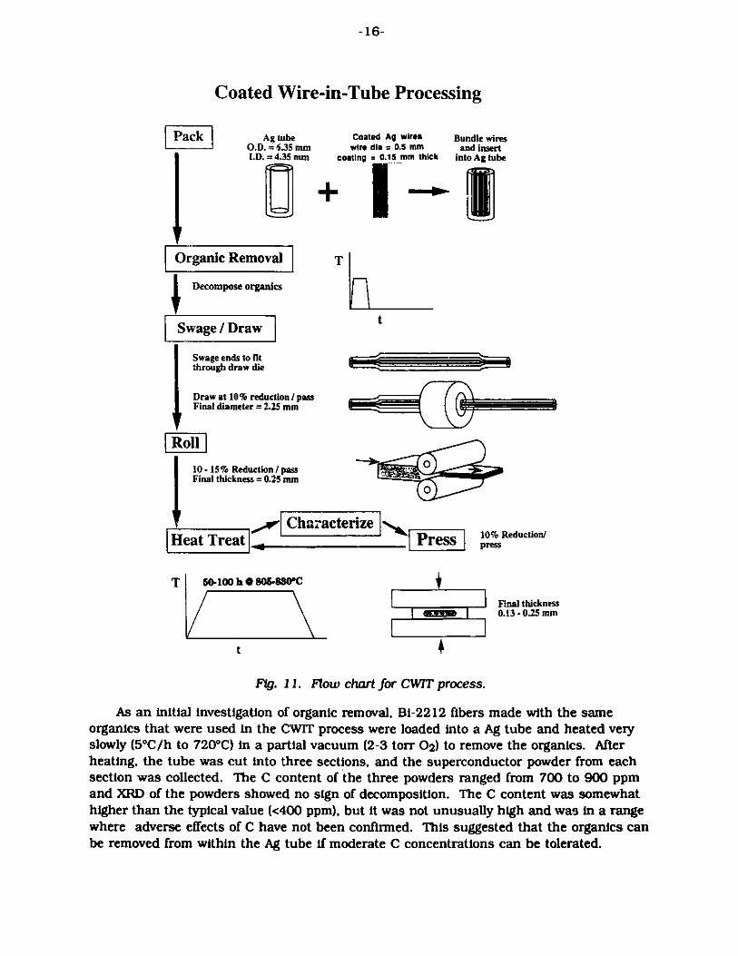
-16-
Coated Wire-in-Tube Processing
Ag tube Coated Ag wires Bundle wiresO.D. =6.35 mm wire dia = 0.5 mm and insertI.D. = 4.35 mm coating = 0.15 mm thick into Ag tube
T
t
Organic Removal
Decompose organics
Swage / Draw
Swage ends to fitthrough draw die
Draw at 10% reduction / passFinal diameter = 2.25 mm
10 - 15% Reduction/ passFinal thickness = 0.25 mm
CharacterizeHeat Treat Press 10% Reduction/
press
T 50.100 h o O805-830C
t
IFinal thickness0.13.0.25 mm
Fig. 11. Flow chart for CWIT process.
As an initial investigation of organic removal, Bi-2212 fibers made with the sameorganics that were used in the CWIT process were loaded into a Ag tube and heated veryslowly (5*C/h to 720*C) in a partial vacuum (2-3 torr 02) to remove the organics. Afterheating, the tube was cut into three sections, and the superconductor powder from eachsection was collected. The C content of the three powders ranged from 700 to 900 ppmand XRD of the powders showed no sign of decomposition. The C content was somewhathigher than the typical value (<400 ppm), but it was not unusually high and was in a rangewhere adverse effects of C have not been confirmed. This suggested that the organics canbe removed from within the Ag tube if moderate C concentrations can be tolerated.
-
Pack
-in
0
I
-17-
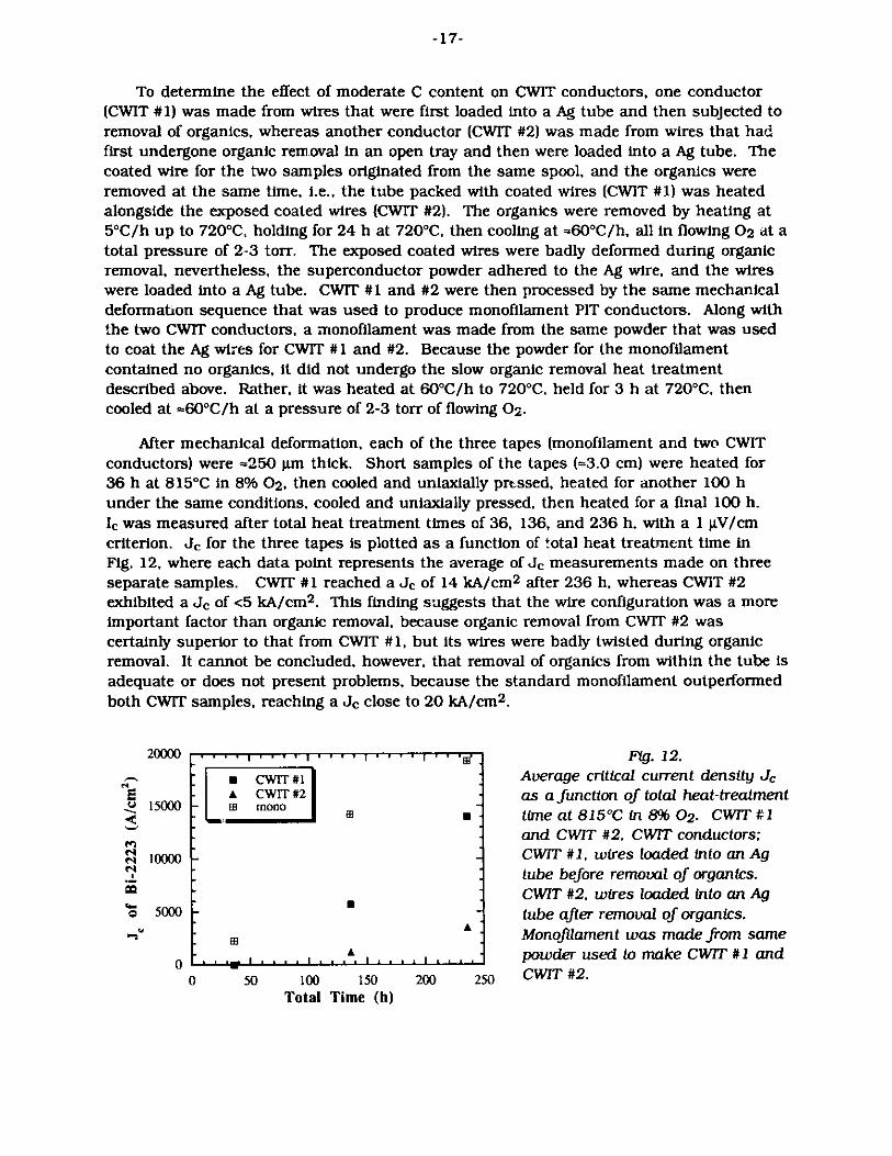
To determine the effect of moderate C content on CWIT conductors, one conductor(CWIT #1) was made from wires that were first loaded into a Ag tube and then subjected to
removal of organics, whereas another conductor (CWIT #2) was made from wires that hadfirst undergone organic removal in an open tray and then were loaded into a Ag tube. Thecoated wire for the two samples originated from the same spool, and the organics wereremoved at the same time, i.e., the tube packed with coated wires (CWIT #1) was heated
alongside the exposed coated wires (CWIT #2). The organics were removed by heating at5*C/h up to 720*C, holding for 24 h at 720*C, then cooling at =60*C/h, all in flowing 02 at a
total pressure of 2-3 torr. The exposed coated wires were badly deformed during organicremoval, nevertheless, the superconductor powder adhered to the Ag wire, and the wireswere loaded into a Ag tube. CWIT #1 and #2 were then processed by the same mechanical
deformation sequence that was used to produce monofilament PIT conductors. Along withthe two CWIT conductors, a monofilament was made from the same powder that was usedto coat the Ag wires for CW1T #1 and #2. Because the powder for the monofilamentcontained no organics, it did not undergo the slow organic removal heat treatmentdescribed above. Rather, it was heated at 60*C/h to 720*C, held for 3 h at 720*C, thencooled at =60*C/h at a pressure of 2-3 torr of flowing 02.
After mechanical deformation, each of the three tapes (monofilament and two CWITconductors) were =250 gm thick. Short samples of the tapes (=3.0 cm) were heated for36 h at 815*C in 8% 02, then cooled and uniaxially pressed, heated for another 100 hunder the same conditions, cooled and uniaxially pressed, then heated for a final 100 h.
Ic was measured after total heat treatment times of 36, 136, and 236 h, with a 1 sV/cmcriterion. Je for the three tapes is plotted as a function of total heat treatment time inFig. 12, where each data point represents the average of Je measurements made on three
separate samples. CWIT #1 reached a Je of 14 kA/cm2 after 236 h, whereas CWIT #2exhibited a Jc of <5 kA/cm2 . This finding suggests that the wire configuration was a moreimportant factor than organic removal, because organic removal from CWIT #2 was
certainly superior to that from CWIT #1, but its wires were badly twisted during organicremoval. It cannot be concluded, however, that removal of organics from within the tube is
adequate or does not present problems, because the standard monofilament outperformedboth CWIT samples, reaching a Je close to 20 kA/cm2 .
20000. . ., . .............. Fig. 12.
Z CWIT #1 Average critical current density Jc
E 15000CIT #2 as a function of total heat-treatment®-8 time at 815*C in 8% 02. CWIT#1
and CWIT #2, CWIT conductors;
10000- CWIT #1, wires loaded into an Agtube before removal of organics.
CWIT #2, wires loaded into an Ag5000 tube after removal of organics.
8 A®Monofilament was made from same
0 "'powder used to make CWIT #1 and
0 50 100 150 200 250 CWIT #2.
Total Time (h)

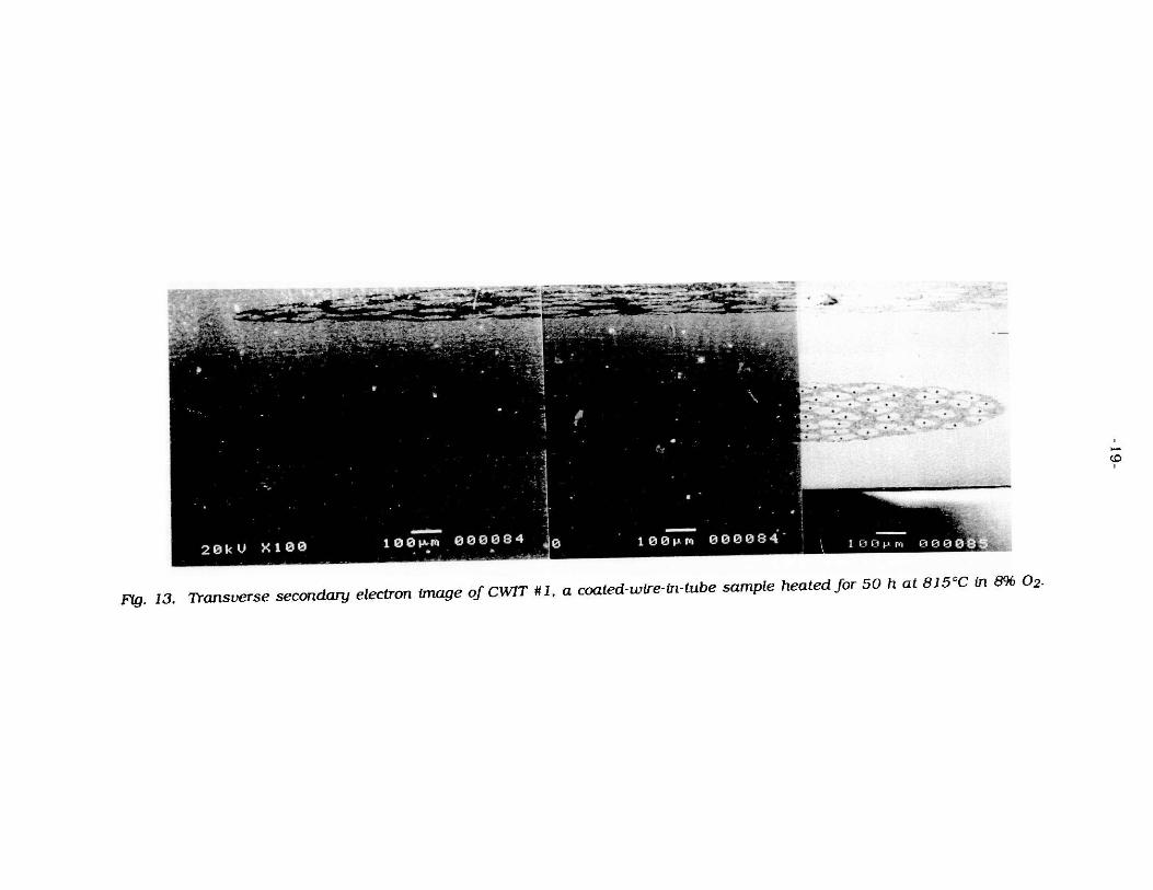
-18-
Figure 13 shows a transverse view of CWIT #1 rolled to an overall tape thickness of1000 pin. The light-colored material around the outside is the Ag sheath; the light-colored oblong shapes are Ag wires (144 in total). The darker material between the Agwires is Bi-2223. Deformation of the wires appears to be fairly uniform in that the wiresare all approximately the same size and the number of wires at the end of the process isthe same as the number of wires put into the tube, within several wires. At a tapethickness of 1000 pm, the Ag wires appear to be distributed uniformly throughout thecore. Examination of thinner tapes, however, shows a less uniform distribution of Ag wiresin the core, suggesting that rolling may cause segregation of the wires. The effect ofmechanical deformation on the Ag wire distribution will be explored in greater detail inthe future.
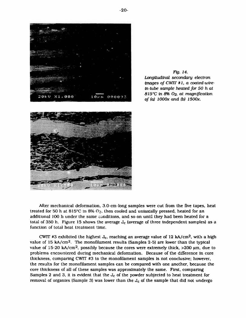
Shown in Fig. 14 are longitudinal views of CW1T #1 rolled to 250 pm. The lightstreaks are Ag wires, and the dark material between the wires is superconductor. Theseviews show that the Ag/superconductor interface is fairly smooth and that the super-conductor thickness (varying between 2 and 10 jm) i uniform along its length. At highermagnification (Fig. 14b), the dense interface layer is evident, but is very thin (only 2-3 Jim)and not completely continuous. It is not clear whether the interface layer must beperfectly continuous to be beneficial, but good continuity is certainly preferred. Toimprove the continuity of the interface layer, and perhaps increase its thickness, Ag wiresthat contained up to several wt.% Pb will beused as the wire inser'.s. Lead plays a crucialrole in the formation of Bi-2223, so its presence in the wires may promote formation ofBi-2223 on their surfaces. In CWIT #2, whose wires were badly deformed during organicremoval, the spatial distribution of Ag wires was less uniform and the superconductorthickness was less uniform in the longitudinal direction, with the Ag wires "pinching off'the superconductor in soire places. These results suggest that the initial wire con-figuration can strongly affect the final microstructure.
Another experiment relating to the removal of organics consisted of five samples.The first sample (CWIT #3) was made from wires that contained organics when they wereloaded into a Ag tube, i.e., the sample was like CWIT #1 except the wires were loaded in astraight and parallel configuration by means of a special rack. Sample 2 was a monofil-ament prepared by our standard PIT procedure with the same powder as in CWIT #3, butthe powder contained no organics. Sample 3 was a monofilament also made from thepowder used for CWIT #3, but the powder was put through the organic removal heattreatment, even though it contained no organics, to see the effect of the heat treatmentitself. Powder for samples 4 and 5 came from the superconductor dispersion used to coatthe wires in CWIT #3, so it contained organics.
Sample 4 was prepared by removing the organics from large chunks of the dispersion(=15-25 sm In diameter) in an open tray, then processing the powder by the normal PITprocedure. Sample 5 was prepared by removing the organics from small chunks of thedispersion (=2-3 pm in diam) placed inside a Ag tube, then processing by the normal PITprocedure. Samples 3, 4, and 5 were positioned side-by-side during the removal oforganics, which was accomplished by heating in 2-3 torr of flowing 02 at 5*C/h up to7200C, holding for 24 h at 7200C, then cooling at =60*C/h.
,-- --
Transverse secondary electron image of CWIT #1, a coated-wire-in-tube sample heated for 50 h at 815 C in 8% 02.Fig. 13.
-20-
Fig. 14.Longitudinal secondary electronimages of CW]T #1, a coated-wire-in-tube sample heated for 50 h at815*C in 8% 02, at magnificationof (a) 1000x and (b) 1500x.
After mechanical deformation, 3.0-cm-long samples were cut from the five tapes, heattreated for 50 h at 815*C in 8% 02. then cooled and uniaxially pressed, heated for anadditional 100 h under the same : anditions, and so on until they had been heated for atotal of 350 h. Figure 15 shows the average Je (average of three independent samples) as afunction of total heat treatment time.
CWIT #3 exhibited the highest Jc, reaching an average value of 12 kA/cm 2 , with a highvalue of 15 kA/cm 2 . The monofilament results (Samples 2-5) are lower than the typicalvalue of 15-20 kA/cm 2 , possibly because the cores were extremely thick, >200 pm, due toproblems encountered during mechanical deformation. Because of the difference in corethickness, comparing CWIT #3 to the monofilament samples is not conclusive; however,the results for the monofilament samples can be compared with one another, because thecore thickness of all of these samples was approximately the same. First, comparingSamples 2 and 3, it is evident that the Jc of the powder subjected to heat treatment forremoval of organies (Sample 3) was lower than the Je of the sample that did not undergo
-^ Wpm"
tazFl

-21-
12000
" 8000 -
V
4000 - _
40 -
D #1
#2
#3
50 150 250 350
Annealing Time (h)
the heat treatment (Sample 2), suggesting that the heat treatment itself damages thesuperconductor. The difference in Jc is not large and should be confirmed, but thedifference is believable, considering that significant phase changes have been shown tooccur in Bi-2223 (Grivel et al., 1993) even at the relatively low temperatures that are usedto remove organics.
Samples 4 and 5 were monofilaments made from the dispersion used to make CWIT#3. Their Je values were nearly identical to one another and were significantly lower thanthe Jc of the monofilaments made without organics (Samples 2 and 3), clearly indicatingthat organic removal can strongly influence the final properties of CWIT conductors. Thesimilarity in Je suggests that the removal of organics was problematic for both samples,from Sample 4 because large chunks of dispersion were used and from Sample 5 becausethe removal was done inside a Ag tube. Both the large size of the dispersion chunks andcontainment by the Ag tube could leave residual carbon and cause decomposition of thesuperconductor during organic removal, possibly accounting for the extremely poor J, ofthese samples. Considering how poorly Samples 4 and 5 performed, presumably due topoor organic removal, the performance of CWIT #3 is startling, possibly indicating that theeffect of Ag wires is beneficial enough to overcome the deleterious impact of organicremoval.
The removal of organics is clearly an important issue, and will be an area of primaryfocus in the future. A CWIT sample whose organics are removed while inside a tube will becompared with one whose organics are removed outside the tube. This will be similar tothe first experiment described above but will be done with a rack to prevent distortion ofthe wires during organic removal. Electrophoretic deposition will be tested as an alter-native method for coating wires, because it produces superconductor coatings that containessentially no organics. Faster organic removal treatments will be explored as a way toavoid disturbing the initial two-powder phase assemblage.
Fig. 15.
Average critical current density Jcas a function of total heat-treatmenttime at 815*C in 8% 02 at 77 K andzero applied field. CWIT #3, acoated-wire-in-tube conductor fromwires that were loaded into an Agtube before removal of organics;Samples 2 and 3, monofilamentsfrom the powder used in CWIT #3;Samples 4 and 5, monofilamentsmade from the superconductordispersion used in CWIT #3.
-22-
The CWIT microstructure will be better characterized and factors affecting themicrostructure will be investigated. The roughness of the Ag/superconductor interfacewill be quantitatively characterized and compared with multifilament conductors. CWITsamples seem to possess fairly smooth Ag/superconductor interfaces, which may be animportant advantage, because grain alignment is more favorable at a smooth interface.A uniform distribution of Ag wires maximizes the effect of Ag, so the distribution of wireswill, be monitored during mechanical deformation to determine the source of nonunifor-mity. Preliminary evidence suggests that rolling may be a source of nonuniformity, sofactors such as tape thickness and conductor geometry (round vs. flat) will be varied togauge their effect on the wire distribution. The crux of the CWlT method is the interfacelayer and how it performs. To improve continuity and perhaps the thickness of theinterface layer, CWIT samples will be processed with Pb in the wires. To address theperformance of the interface layer, CWIT samples will be studied by magneto-opticalimaging. Finally, to test the expectation that these samples should exhibit strain tolerancecomparable to that of multifilament samples, strain tolerance of CWIT samples will bemeasured.
Strain Tolerance of Tapes
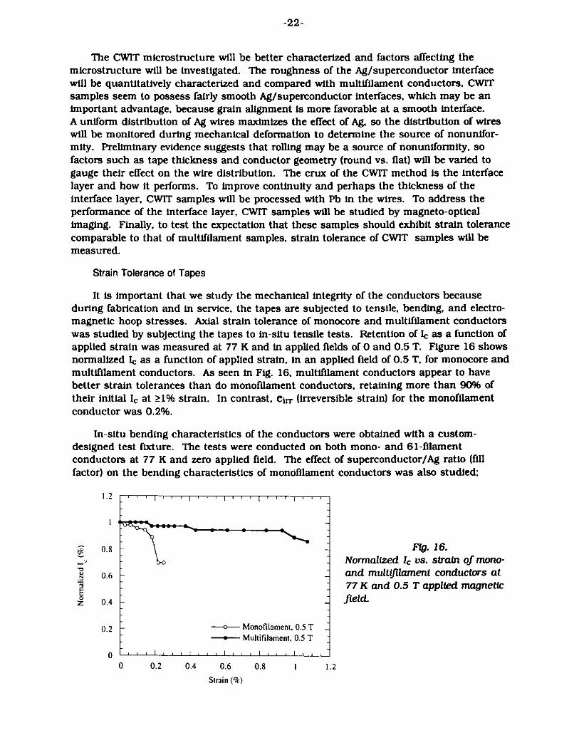
It is important that we study the mechanical integrity of the conductors becauseduring fabrication and in service, the tapes are subjected to tensile, bending, and electro-magnetic hoop stresses. Axial strain tolerance of monocore and multifilament conductorswas studied by subjecting the tapes to in-situ tensile tests. Retention of Ic as a function ofapplied strain was measured at 77 K and in applied fields of 0 and 0.5 T. Figure 16 showsnormalized Ic as a function of applied strain, in an applied field of 0.5 T, for monocore andmultifilament conductors. As seen in Fig. 16, multifilament conductors appear to havebetter strain tolerances than do monofilament conductors, retaining more than 90% oftheir initial Ic at 1% strain. In contrast, eirr (irreversible strain) for the monofilamentconductor was 0.2%.
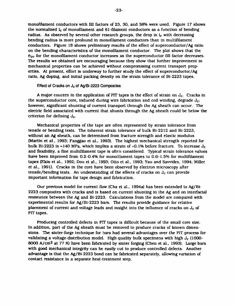
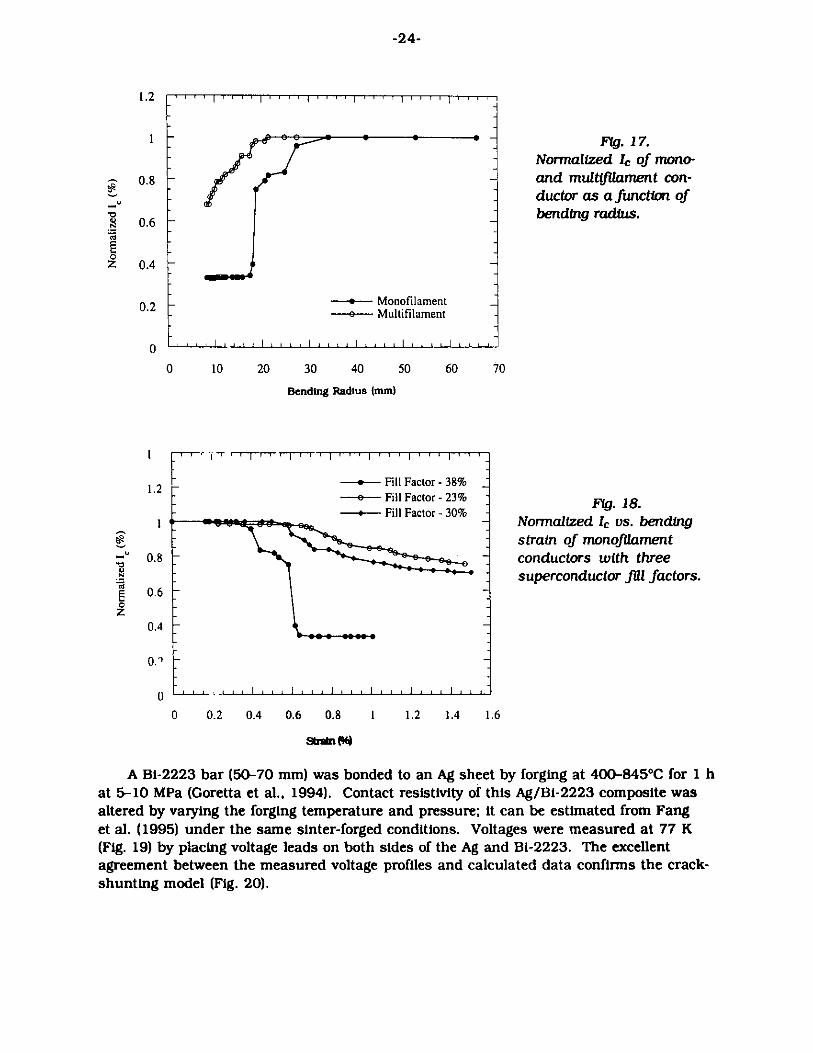
In-situ bending characteristics of the conductors were obtained with a custom-designed test fixture. The tests were conducted on both mono- and 61-filamentconductors at 77 K and zero applied field. The effect of superconductor/Ag ratio (fillfactor) on the bending characteristics of monofilament conductors was also studied;
1.2
0.8 1-Fig. 16.Normalized Ic vs. strain of mono-
0.6 and multifilament conductors at77 K and 0.5 T applied magnetic
z 0.4 field.
0.2 -0---~ Monofilament, 0.5 T- Multifilament, 0.5 T
0
0 0.2 0.4 0.6 0.8 1 1.2
Strain (%)
-23-
monofilament conductors with fill factors of 23, 30, and 38% were used. Figure 17 showsthe normalized Ic of monofilament and 61-filament conductors as a function of bendingradius. As observed by several other research groups, the drop in Ic with decreasingbending radius is more profound in monofilament conductors than in multifilamentconductors. Figure 18 shows preliminary results of the effect of superconductor/Ag ratioon the bending characteristics of the monofilament conductor. The plot shows that theeirr for the monofilament conductor increases as the superconductor fill factor decreases.The results we obtained are encouraging because they show that further improvement inmechanical properties can be achieved without compromising current transport prop-erties. At present, effort is underway to further study the effect of superconductor/Agratio, Ag doping, and initial packing density on the strain tolerance of Bi-2223 tapes.
Effect of Cracks on Jc of Ag/Bi-2223 Composites
A major concern in the application of PIT tapes is the effect of strain on Jc. Cracks inthe superconductor core, induced during wire fabrication and coil winding, degrade Jc;however, significant shunting of current transport through the Ag sheath can occur. Theelectric field associated with current that shunts through the Ag sheath could be below thecriterion for defining Jc.
Mechanical properties of the tape are often represented by strain tolerance fromtensile or bending tests. The inherent strain tolerance of bulk Bi-2212 and Bi-2223,without an Ag sheath, can be determined from fracture strength and elastic modulus(Martin et al., 1993; Fanggao et al., 1993). The highest mechanical strength reported forbulk Bi-2223 is =140 MPa, which implies a strain of ~0.1% before fracture. To increase Jand flexibility, a fine multifilament tape is often considered. Typical strain tolerance valueshave been improved from 0.2-0.4% for monofilament tapes to 0.6-1.5% for multifilamenttapes (Ekin et al., 1992; Dou et al., 1993; Otto et al., 1993; Yau and Savvides, 1994; Milleret al., 1991). Cracks in the core have been observed by electron microscopy aftertensile/bending tests. An understanding of the effects of cracks on Je can provideimportant information for tape design and fabrication.
Our previous model for current flow (Cha et al., 1994a) has been extended to Ag/Bi-2223 composites with cracks and is based on current shunting in the Ag and on interfacialresistance between the Ag and Bi-2223. Calculations from the model are compared withexperimental results for Ag/Bi-2223 bars. The results provide guidance for relativeplacement of current and voltage leads and insight into the influence of cracks on Jc ofPIT tapes.
Producing controlled defects in PIT tapes is difficult because of the small core size.In addition, part of the Ag sheath must be removed to produce cracks of known dimen-sions. The sinter-forge technique for .bars had several advantages over the PIT process forvalidating a voltage-distribution model. High-quality bulk specimens with high Je (1000-8000 A/cm2 at 77 K) have been fabricated by sinter forging (Chen et al., 1993). Large barswith good mechanical integrity can be easily cut to produce controlled defects. Anotheradvantage is that the Ag/Bi-2223 bond can be fabricated separately, allowing variation ofcontact resistance in a separate heat-treatment step.
-24-
Fig. 17.Normalized Ic of mono-and multiflament con-ductor as a function ofbending radius.
1.2
1
0.8
0.6
0.4
0.2
0
Fig. 18.Normalized Ic vs. bendingstrain of monofilamentconductors with threesuperconductor fill factors.
0 0.2 0.4 0.6 0.8 1 1.2 1.4 1.6
Sbin (4
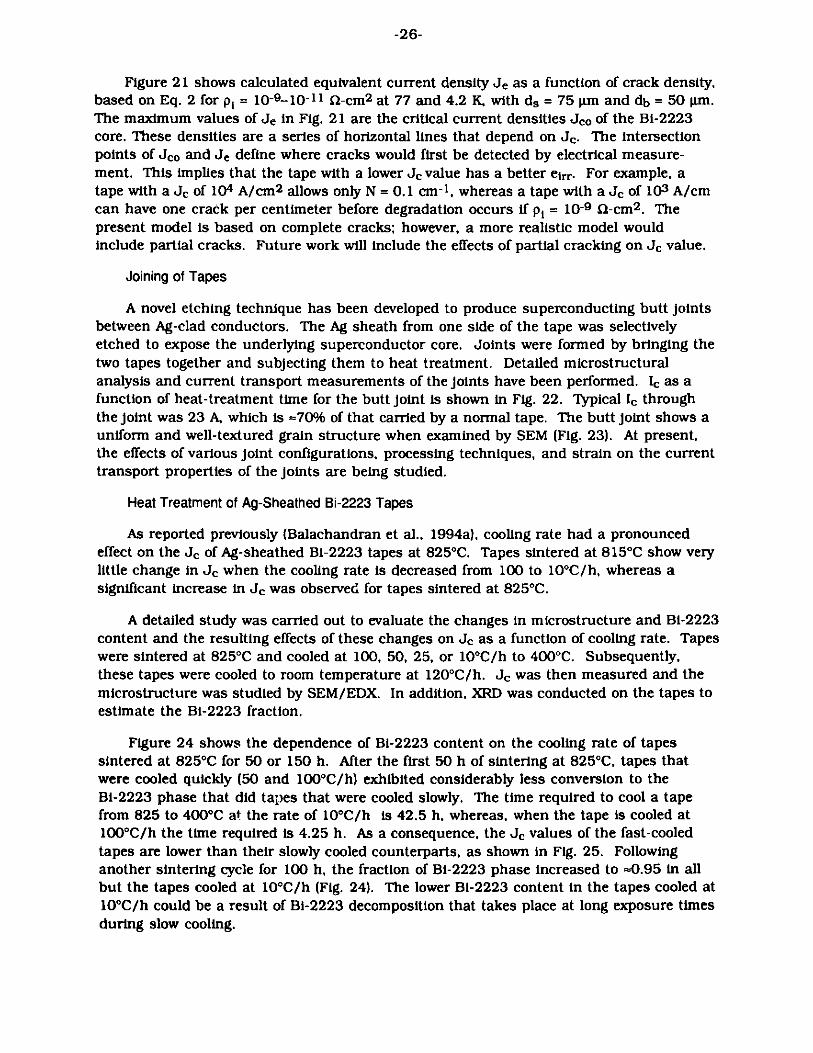
A Bi-2223 bar (50-70 mm) was bonded to an Ag sheet by forging at 400-845*C for 1 hat 5-10 MPa (Goretta et al., 1994). Contact resistivity of this Ag/Bi-2223 composite wasaltered by varying the forging temperature and pressure; it can be estimated from Fanget al. (1995) under the same sinter-forged conditions. Voltages were measured at 77 K(Fig. 19) by placing voltage leads on both sides of the Ag and Bi-2223. The excellentagreement between the measured voltage profiles and calculated data confirms the crack-shunting model (Fig. 20).
N
--- Monofilament-e--Multifilament
0 10 20 30 40 50 60 70
Bending Radius (mm)
1.2
N
0
z
1 '
0.8
0.6
0.4
0.'
0
t_ Fill Factor-38% _
----- Fill Factor - 23%---- Fill Factor - 30% -
I I-I

-25-
L Fig. 19.V_ -_0)_=VbVoltage lead placement in Ag/Bi-2223
BSCCC -4 specimen.
V8(0) V8 (x) V(L)I 0}--- x I
600T=77K
500 Fig. 20.
400 P = 3x10 5f-cm2 Line fit of voltage drop along Ag forsinter-forged Ag/Bi-2223, deter-
> 300 p = 2x10'5 n-cn 2 mined from model; experimentala data are individual data points.
200P = 2x10 f-cm2
100 - -P = 2x10 7f-cm2
00 1 2 3 4 5 6 7 8
Distance, x (cm)
When a complete crack is present in the Bi-2223 core, all of the current is forced toshunt into the Ag via the interface. The voltage associated with current shunting is low andis manifested as a li; ear rise in the V-I curve at current densities below the core Jc. Suchbehavior has been ol.served for V-I curves; however, high electric field sensitivity, i.e.,=1 nV/cm, is required (Suenaga et al., 1995).
Voltage drop in the Je measurement is the sum of the voltage across the Ag/BSCCOinterface (2Vb) and the voltage of the Ag in the crack zone. The voltage can be rewritten interms of the current density (J = Io/wdb) for the tape
Vb = Jdb PsPi , (1)2 d'
as long as AL > 10. If Je degradation is caused by the cracks in the core, use of 2Vb = Vcand J = Je can yield the equivalent current density Je in a tape with multiple cracks, i.e.,
Je d=b d (2)
where Ec (1 gV/cm) is the critical field and N is crack density (number of cracks per cm).This suggests that Je is proportional to the square root of ds and inversely proportional toN and db. Je in Eq. 2 cannot be exceeded by the core Jc.
-26-
Figure 21 shows calculated equivalent current density Je as a function of crack density,based on Eq. 2 for pi = 10-9-10-11 S-cm2 at 77 and 4.2 K, with ds = 75 p.m and db = 50 pm.The maximum values of Je in Fig. 21 are the critical current densities Jco of the Bi-2223core. These densities are a series of horizontal lines that depend on Jc. The intersectionpoints of Jco and Je define where cracks would first be detected by electrical measure-ment. This implies that the tape with a lower Je value has a better eirr. For example, atape with a Jc of 104 A/cm 2 allows only N = 0.1 cm- 1, whereas a tape with a Je of 103 A/cmcan have one crack per centimeter before degradation occurs if pi = 10-9a -cm2 . Thepresent model is based on complete cracks; however, a more realistic model wouldinclude partial cracks. Future work will include the effects of partial cracking on Jc value.
Joining of Tapes
A novel etching technique has been developed to produce superconducting butt jointsbetween Ag-clad conductors. The Ag sheath from one side of the tape was selectivelyetched to expose the underlying superconductor core. Joints were formed by bringing thetwo tapes together and subjecting them to heat treatment. Detailed microstructuralanalysis and current transport measurements of the joints have been performed. Ic as afunction of heat-treatment time for the butt joint is shown in Fig. 22. Typical Ic throughthe joint was 23 A, which is =70% of that carried by a normal tape. The butt joint shows auniform and well-textured grain structure when examined by SEM (Fig. 23). At present,the effects of various joint configurations, processing techniques, and strain on the currenttransport properties of the joints are being studied.
Heat Treatment of Ag-Sheathed Bi-2223 Tapes
As reported previously (Balachandran et al., 1994a), cooling rate had a pronouncedeffect on the Jc of Ag-sheathed Bi-2223 tapes at 825*C. Tapes sintered at 815*C show verylittle change in Je when the cooling rate is decreased from 100 to 10*C/h, whereas asignificant increase in Je was observed for tapes sintered at 825*C.
A detailed study was carried out to evaluate the changes in microstructure and Bi-2223content and the resulting effects of these changes on Jc as a function of cooling rate. Tapeswere sintered at 825*C and cooled at 100, 50, 25, or 10*C/h to 400*C. Subsequently,these tapes were cooled to room temperature at 120*C/h. Je was then measured and themicrostructure was studied by SEM/EDX. In addition, XRD was conducted on the tapes toestimate the Bi-2223 fraction.
Figure 24 shows the dependence of Bi-2223 content on the cooling rate of tapessintered at 825*C for 50 or 150 h. After the first 50 h of sintering at 825*C, tapes thatwere cooled quickly (50 and 100*C/h) exhibited considerably less conversion to theBi-2223 phase that did tapes that were cooled slowly. The time required to cool a tapefrom 825 to 400*C at the rate of 10*C/h is 42.5 h, whereas, when the tape is cooled at100*C/h the time required is 4.25 h. As a consequence, the Je values of the fast-cooledtapes are lower than their slowly cooled counterparts, as shown in Fig. 25. Followinganother sintering cycle for 100 h, the fraction of Bi-2223 phase increased to ~0.95 in allbut the tapes cooled at 10*C/h (Fig. 24). The lower Bi-2223 content in the tapes cooled at10*C/h could be a result of Bi-2223 decomposition that takes place at long exposure timesduring slow cooling.

-27-
106
105
10'
103
1021
Number of cracks per cm
-
-L
---- Normal Tape
---- Butt joint
21
FIg. 21.Calculated degradation of Jc varyingwith crack density in Bi-2223 for tapeat 77 K (solid lines) and 4.2 K
(dashed lines).
10
Fig. 22.Ic as function of heat-treatment timefor butt Joint and normal tape.
0 100 200 300 400
Heat'Teatment 'nn (h)
Microstructural studies on these tapes etched in 1% butoxy ethanol in perchloric acidshow a clear trend in core evolution. Increases in volume fraction of the interconnectedBi-2223 grains were observed with decreasing cooling rate (Fig. 26). Increase in grainconnectivity provides an uninterrupted current path and, hence, high Jc. The optimumcombination of phase purity and core density was attained in the tapes cooled at 25*C/h.These tapes yielded the highest average J (=25,500 A/cm 2 at 77 K), which is =40% higher
than the Je values obtained for the tapes cooled at 100*C/h.
Based on the above results, a cooling schedule that employs two or more steps wasimplemented. The objective of the new schedule was to benefit from the slow cooling rate(10*C/h) during the initial stages of cooling (825 to 800*C) and to use a faster cooling ratebelow 800*C (25*C/h) to minimize dissociation of the Bi-2223 phase to Bi-2212 and sec-ondary phases. Such a schedule promotes formation of dense, phase-pure cores. Figure 27shows the Bi-2223 content obtained with various cooling schedules for tapes sintered at
0.1
NE
-- 4.2 K
- --- - =10" -cmJ =-T -A/c 2 --
C*-o - -- - - ~ - -- - -
--- -J
J =10 -... 10'2' - -.- - - -
1011
Jo =i03 A/cm2 Je
77K
.. . . .J.. .l
50
40
30
20
10
0 _s -- ,
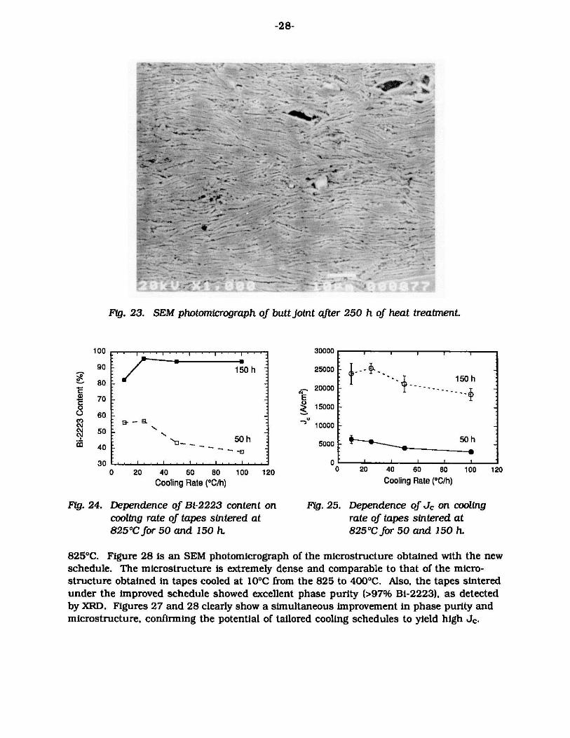
-28-
A.7.
"-- " y~
Fig. 23. SEM photomicrograph of butt joint after 250 h of heat treatment.
-.-
150h
---. 50 h
I ' - - - ' - - ' - . .
0 20 40 60 80Cooling Rate (*C/h)
0
V
... ,.u
30000
25000
20000
15000
10000
5000
0
100 120
Fig. 24. Dependence of Bi-2223 content oncooling rate of tapes sintered at825*C for 50 and 150 n.
0 20 40 60 80
Cooling Rate (*C/h)
FIg. 25. Dependence of Jc on coolingrate of tapes sintered at825*C for 50 and 150 h.
8250C. Figure 28 is an SEM photomicrograph of the microstructure obtained with the newschedule. The microstructure is extremely dense and comparable to that of the micro-structure obtained in tapes cooled at 100C from the 825 to 4000C. Also, the tapes sinteredunder the improved schedule showed excellent phase purity (>97% Bi-2223), as detectedby XRD. Figures 27 and 28 clearly show a simultaneous improvement in phase purity andmicrostructure, confirming the potential of tailored cooling schedules to yield high Jc.
0c
C
O0NNV
C"
100
90
80
70
60
50
40
30
- - . - ,150h
- 50 h
p
100 120
Fr
-. 1W
,
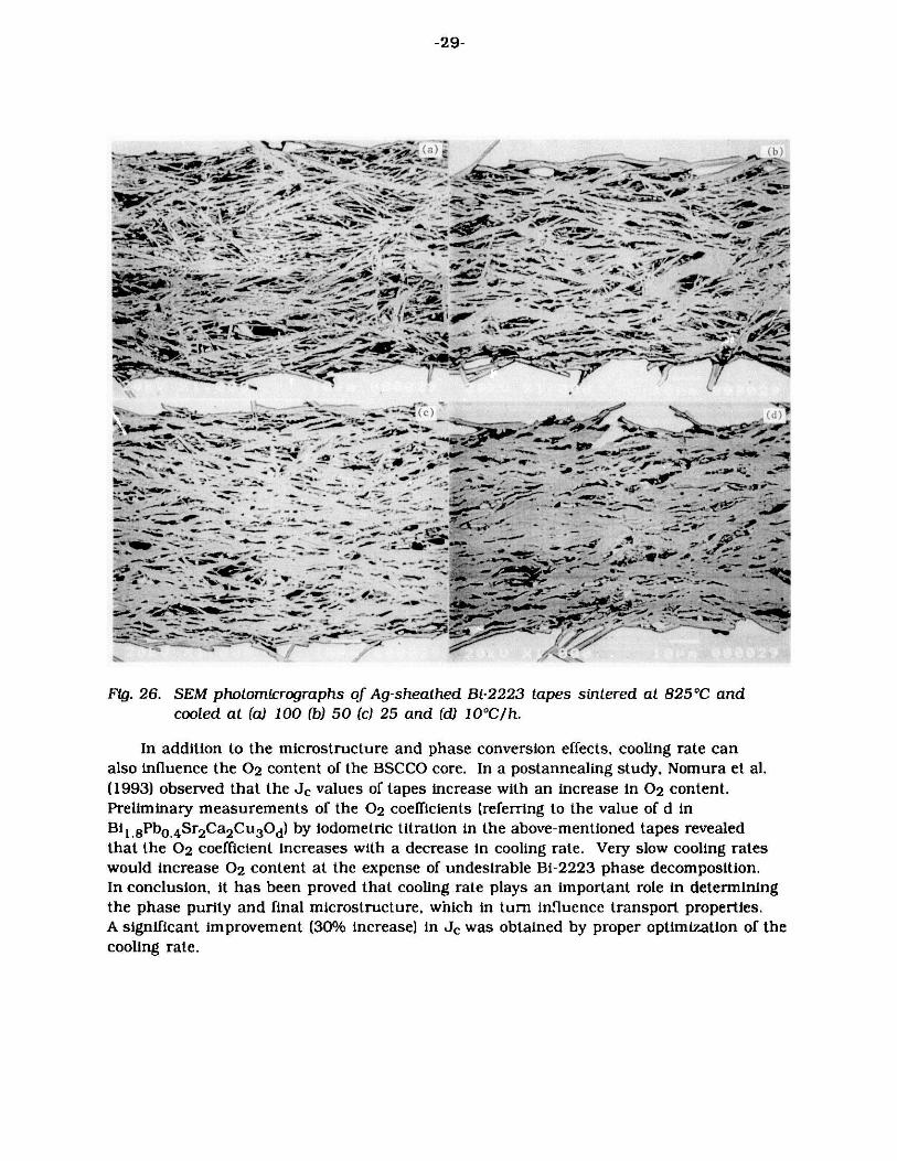
-29-
...- --r -- -, - -
-- - - ~-~ - . .
cooled a ) 100 "b) 5 - :c) 5 an (. 0*C. -.
te- N --t ' 4 "- r "t r..- -' f1. - r. -
-" _+ - --c 4 Z.-
In addion o ". he mcrostruure and phas nvr s- ees n rate/ Can
s infene he -21!nent ofI the BSC core.. I -'rtn n study Nour et a..
) eJ s e se2
P mn s me he
10~ ..' I
Big.b 46.SEMa2s phtmcygah toerf Ag-shathen i222heaementerned t825s eeaned
Iha addtio to thfce icreosesrwctr an dehrase incovesin e.eryss, cooling rates
would increase 02 content at the expense of undesirable Bi-2223 phase decomposition.
In conclusion, it has been proved that cooling rate plays an important role in determining
the phase purity and final microstructure, which in turn influence transport properties.
A significant improvement (30% increase) in Je was obtained by proper optimization of the
cooling rate.
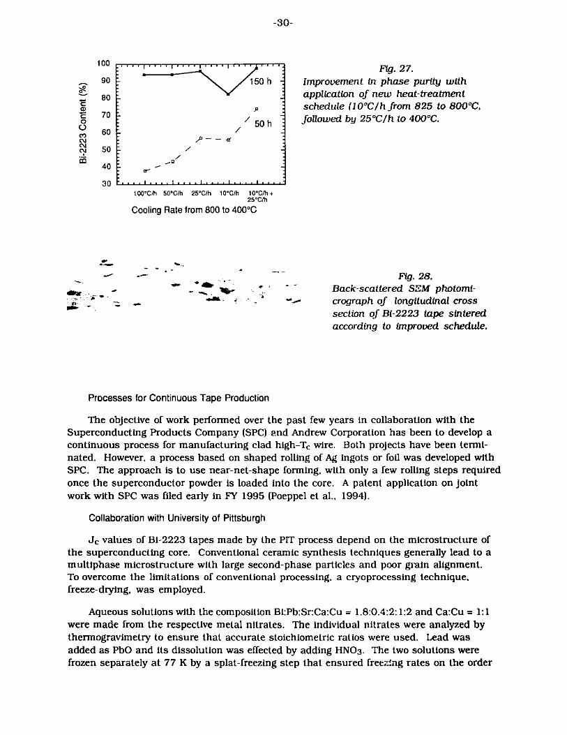
-30-
100 Fig 27.
90 150 h Improvement in phase purity with
80 application of new heat-treatmentEC schedule (10*C/h from 825 to 800*C,
70 50 h followed by 25*C/h to 400*C.60-
c'JN j50 -
40
30--
100C/ 50*C/h 25*C/h 10OC/h 10*C/h +25*C/h
Cooling Rate from 800 to 400*C
- Fig. 28.__0 .Back-scattered SEM photomi-
,..a- crograph of longitudinal cross
section of B-2223 tape sinteredaccording to improved schedule.
Processes for Continuous Tape Production
The objective of work performed over the past few years in collaboration with theSuperconducting Products Company (SPC) and Andrew Corporation has been to develop acontinuous process for manufacturing clad high-Ta wire. Both projects have been termi-nated. However, a process based on shaped rolling of Ag ingots or foil was developed with
SPC. The approach is to use near-net-shape forming, with only a few rolling steps requiredonce the superconductor powder is loaded into the core. A patent application on jointwork with SPC was filed early in FY 1995 (Poeppel et al., 1994).
Collaboration with University of Pittsburgh
J values of BI-2223 tapes made by the PIT process depend on the microstructure ofthe superconducting core. Conventional ceramic synthesis techniques generally lead to amultiphase microstructure with large second-phase particles and poor grain alignment.To overcome the limitations of conventional processing, a cryoprocessing technique,freeze-drying, was employed.
Aqueous solutions with the composition Bi:Pb:Sr:Ca:Cu = 1.8:0.4:2:1:2 and Ca:Cu = 1:1were made from the respective metal nitrates. The individual nitrates were analyzed bythermogravimetry to ensure that accurate stoichiometric ratios were used. Lead wasadded as PbO and its dissolution was effected by adding HNO3. The two solutions werefrozen separately at 77 K by a splat-freezing step that ensured frees-ng rates on the order

-31-
of 105 K/s. The frozen solutions were then mixed in liquid N2 with a high-shear homog-enizing tool. The resultant frozen sample was then dried according to the proceduredescribed by Krishnaraj et al. (1993). The dried and mixed precursors were denitrated byflash heating at 780-820*C for 1-2 h. The resultant powder was packed into Ag tubes andprocessed into tapes. The evolution of the Bi-2223 phase was studied by XRD and themicrostructure was studied by SEM coupled with EDX.
X-ray diffraction data for freeze-dried Pb-2212 samples that were heat treated forvarious times in 100% 02 at 8200C are shown in Fig. 29. The high reactivity of thepowders is seen from the short times required for the formation of Bi-2212. After 4 h, theprimary phase is Bi-2212, and after 8 h, the sample is seen to be single-phase Bi-2212,within the limits of detection by XRD. The tapes were then heat treated in 7% 02 at8150C, the onset temperature of the reaction to form the Bi-2223 phase, as seen from theDTAX data of Fig. 30. Bi-2223 is the primary phase after 24 h; after 50 h the tapes appearto be almost single-phase Bi-2223. This, once again, establishes the high reactivity of thepowder. The freeze-drying process yielded a homogeneous precursor, with high massthroughput, allowing easy scale-up of the process for synthesis of large quantities ofprecursors for the manufacture of long lengths of superconducting tapes.
The thin superconducting region next to the Ag sheath appears to be the region ofmaximum Jc (>100,000 A/cm2 at 77 K) in Bi-2223 tapes (Larbalestier et al., 1994; Lelovicet al., 1995a and b). Transport measurements on Bi-2223 tape at 77 K in low magneticfield applied parallel to the tape thickness indicate an exponential field dependence fortransport currents. Magnetic hysteresis was measured in a 10-sm-thick layer of supercon-ductor near the Ag sheath as a function of temperature, intensity, and orientation ofapplied field with respect to the tape. The characteristic field for full penetration depthfor a superconducting slab was found to have a power-law dependence on temperature.Magnetization currents as a function of temperature and applied field oriented parallel tothe tape thickness were determined from the width of the magnetization loop with a Bean-model expression adapted for an orthorhombic sample. The critical-state model, adjustedfor scaling and magnetic relaxation, correlates well with the magnetization current of thethin layer at 77 K (Lelovic et al., 1995b).
If the interfacial length of contact between the Ag sheath and core with respect to thetransverse cross section of the tape is increased, the current-carrying capacity of the tapesshould improve. The length of interface between the superconducting core and the Agsheath is defined here as the interface perimeter length (IPL) (Fig. 31), and increasing itshould result in a measured increase in critical current. To compare tapes of different IPLwith each other, they must have the same cross-sectional area; this can be attained byvarying the mechanical-working procedures. Thus, the performance of a tape may beimproved by changing its geometry.
To obtain wires with various IPL values but identical cross-sectional area, themechanical-working schedule was altered. Three Ag tubes with powders were preparedfor drawing and rolling operations. Of the three tubes, the first was drawn to a diameter of4,064 pm, the second to 3,048 m, and the third to 2,032 m. After drawing, they wererolled to thicknesses at which their cross-sectional areas were identical. The first wasrolled to a thickness of 254 jm, the second to 383 pm, and the third to 508 m. Figure32 shows the relative shapes and dimensions of the finished composite tapes. The IPL ofthe first is twice that of the third and 1.5 times that of the second. A wider range of IPLs
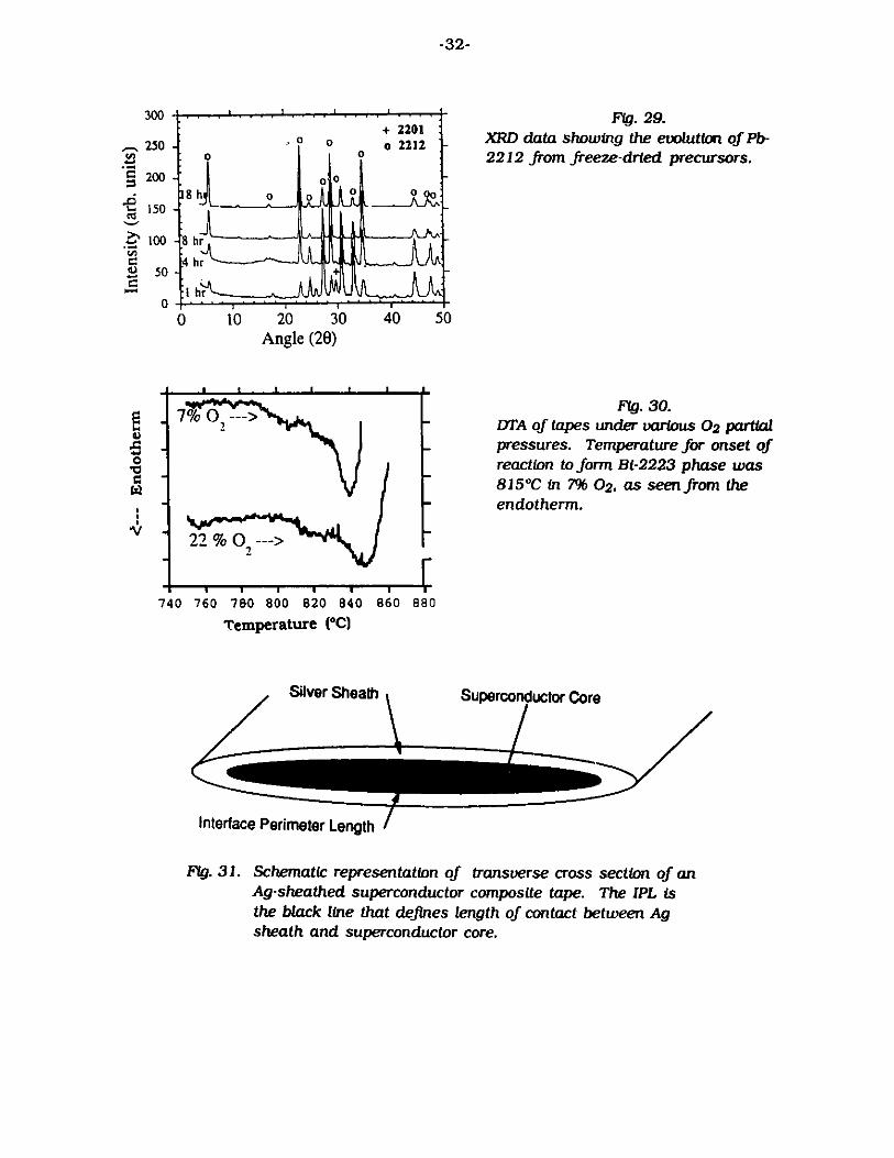
Fig. 29.XRD data showing the evolution of Pb-2212 from freeze-dried precursors.
250
200
150
I100
3 50
0
Fig. 30.DTA of tapes under various 02 partialpressures. Temperature for onset ofreaction to form Bi-2223 phase was815*C in 7% 02. as seen from theendotherm.
7- -
760 780 800 820 840 860
Temperature (*C)
8880
Silver Sheath Superconductor Core
Interface Perimeter Length
Fig. 31. Schematic representation of transverse cross section of anAg-sheathed superconductor composite tape. The IPL isthe black line that defInes length of contact between Agsheath and superconductor core.
-32-
+ 22010 0 o2212 -
0 *0
18 hr
4 hr
I hrIr ----
300
10 20 30 40 50Angle (28)
014
O5-
-W
0
'i z
740
I 1 1 1 1 1
1
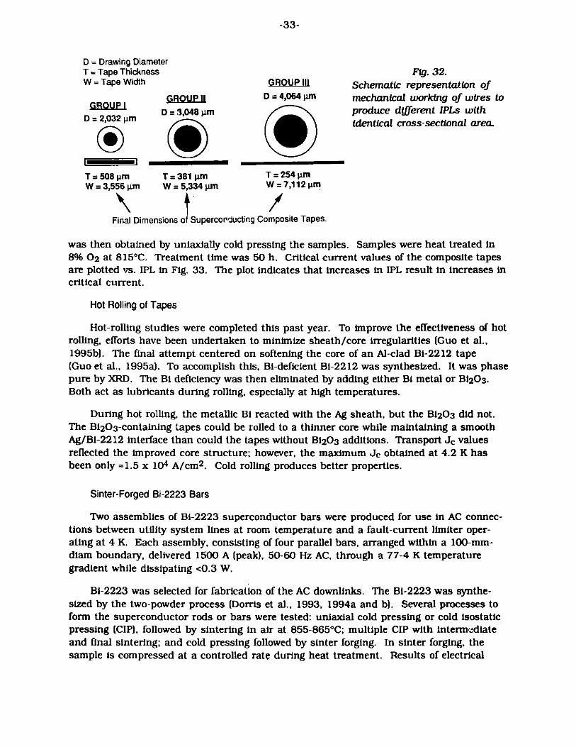
-33-
D = Drawing DiameterT = Tape ThicknessW = Tape Width
GROD = 2,0
T = 501W = 3,
32 pm
GROUP 4D = 3,048 pm
( )
GROUP II
D = 4,064 m
Fig. 32.Schematic representation ofmechanical working of wires toproduce different IPLs withidentical cross-sectional area.
8p m T=381pm T=254p m556 m W = 5,334 m W = 7,112 pm
Final Dimensions of Superconducting Composite Tapes.
was then obtained by uniaxially cold pressing the samples. Samples were heat treated in8% 02 at 815*C. Treatment time was 50 h. Critical current values of the composite tapesare plotted vs. IPL in Fig. 33. The plot indicates that increases in IPL result in increases incritical current.
Hot Rolling of Tapes
Hot-rolling studies were completed this past year. To improve the effectiveness of hotrolling, efforts have been undertaken to minimize sheath/core irregularities (Guo et al.,1995b). The final attempt centered on softening the core of an Al-clad Bi-2212 tape(Guo et al., 1995a). To accomplish this, Bi-deficient Bi-2212 was synthesized. It was phasepure by XRD. The Bi deficiency was then eliminated by adding either Bi metal or B1 2 03.Both act as lubricants during rolling, especially at high temperatures.
During hot rolling, the metallic Bi reacted with the Ag sheath, but the Bi203 did not.The Bi203-containing tapes could be rolled to a thinner core while maintaining a smoothAg/Bi-2212 interface than could the tapes without Bi 203 additions. Transport Je valuesreflected the improved core structure; however, the maximum Je obtained at 4.2 K hasbeen only =1.5 x 10⁴ A/cm 2. Cold rolling produces better properties.
Sinter-Forged Bi-2223 Bars
Two assemblies of BI-2223 superconductor bars were produced for use in AC connec-tions between utility system lines at room temperature and a fault-current limiter oper-ating at 4 K. Each assembly, consisting of four parallel bars, arranged within a 100-mm-diam boundary, delivered 1500 A (peak), 50-60 Hz AC, through a 77-4 K temperaturegradient while dissipating <0.3 W.
BI-2223 was selected for fabrication of the AC downlinks. The Bi-2223 was synthe-sized by the two-powder process (Dorris et al., 1993, 1994a and b). Several processes toform the superconductor rods or bars were tested: uniaxial cold pressing or cold isostaticpressing (CIP), followed by sintering in air at 855-865*C; multiple CIP with intermediateand final sintering; and cold pressing followed by sinter forging. In sinter forging, thesample is compressed at a controlled rate during heat treatment. Results of electrical
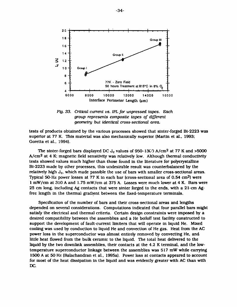
-34-
20-
1 8 -- Group II
16
14-Group I
~12
10 - GroupI-
8
6 77K - Zero Field50 hours Treatment at 815*C in 8%
46000 8000 10000 12000 14000 16000
Interface Perimeter Length (m)
Fig. 33. Critical current vs. IPL for unpressed tapes. Eachgroup represents composite tapes of differentgeometry but identical cross-sectional area.
tests of products obtained by the various processes showed that sinter-forged Bi-2223 wassuperior at 77 K. This material was also mechanically superior (Martin et al., 1993;Goretta et al., 1994).
The sinter-forged bars displayed DC Je values of 950-1369 A/cm2 at 77 K and >5000A/cm2 at 4 K; magnetic field sensitivity was relatively low. Although thermal conductivitytests showed values much higher than those found in the literature for polycrystallineBi-2223 made by other processes, this undesirable result was counterbalanced by therelatively high Je, which made passible the use of bars with smaller cross-sectional areas.Typical 50-Hz power losses at 77 K in each bar (cross-sectional area of 0.54 cm2 ) were1 mW/cm at 310 A and 1.75 mW/cm at 375 A. Losses were much lower at 4 K. Bars were25 cm long, including Ag contacts that were sinter forged to the ends, with a 21-cm Ag-free length in the thermal gradient between the fixed-temperature terminals.
Specification of the number of bars and their cross-sectional areas and lengthsdepended on several considerations. Computations indicated that four parallel bars mightsatisfy the electrical and thermal criteria. Certain design constraints were imposed by adesired compatibility between the assemblies and a He boiloff test facility constructed tosupport the development of fault-current limiters that will operate in liquid He. Mixedcooling was used by conduction to liquid He and convection of He gas. Heat from the ACpower loss in the superconductor was almost entirely removed by convecting He, andlittle heat flowed from the bulk ceramic to the liquid. The total heat delivered to theliquid by the two downlink assemblies, their contacts at the 4.2 K terminal, and the low-temperature superconductor linkage between the assemblies was 517 mW while carrying1500 A at 50 Hz (Balachandran et al., 1995a). Power loss at contacts appeared to accountfor most of the heat dissipation in the liquid and was evidently greater with AC than withDC.
-35-
2.2 TI-M-Sr-Ba-Ca-Cu-O Superconductors
The goal of this part of the ANL program is to develop a useful conductor for high-temperature, high-field applications, with T1-1223 being the most promising candidate atpresent. The rationale is that T1-1223 has improved flux-pinning properties at 77 K whencompared with Bi-2223 (Balachandran et al., 1994a), and the potential for improvedintergranular coupling, first demonstrated by General Electric (GE) (DeLuca et al., 1992).Our progress has indicated that good phase purity and grain alignment are necessary, butnot sufficient, to obtain the highest Jc in T1-1223. It also is necessary to avoid significantintergranular weak links. Processing in the presence of a transient liquid phase seems tobe a very effective way to accomplish this in bulk forms.
We continue to study synthesis and processing procedures that will overcome theintergranular weak-link problem in T1-1223. Our approach is to concentrate on findingand using transient liquid phases at the crucial step in processing to assist in grainorientation and improved intergranular connectivity, while preserving reasonable phasepurity. This program includes various PIT configurations, thick (20-50 m) coatings, andthin films; much of it involves research agreements with GE, Intermagnetics GeneralCorporation (IGC), State University of New York at Buffalo (SUNY-Buffalo), and theThallium Working Group.
2.2.1 Ag-Clad TI-1223 Tapes and Wires
Composition Studies
Bismuth and Pb substitution in T1-1223 superconductors has been used extensively toincrease Tc (Paranthaman and Hermann, 1994; Ren and Wang, 1993; Ren et al., 1995) andflux pinning, and stabilize the superconductor phase (Ren et al., 1995). The goals of thiswork were to find the role of Bi substitution in T1-1223 in phase development of Ag-cladtapes and to determine how Bi substitution influences the melting behavior of T1-1223.Liquids with excess Bi are common in other superconductor compounds (Schartman,1993), and Bi oxides are less volatile than TI oxides (Holstein, 1994).
Differential thermal analysis was used to determine the effect of Bi substitution onmelting temperature (Fig. 34).
A single melting event was observed for x = 0 and x = 0.22, and was ascribed to theincongruent melting of T1-1223. The melting point increased with Bi substitution until thesolubility limit of T1-1223 was exceeded. A low-temperature endotherm was observed forBi substitutions >x = 0.22. The second endotherm correlates with the presence of BaBiO3from XRD data and suggests the possibility of a eutectic melt between impurity phases.The size of this endotherm increases with increasing Bi substitution.
SEM photomicrographs of calcined powder revealed that the particle size wassignificantly larger for high Bi content (Fig. 35).
Significant grain growth in TI-based superconductors has been attributed to thepresence of a liquid phase (Morgan et al., 1990). Results from EDX confirmed that theobserved large platelike particles were T1-1223.

-36-
0
-50
-100
Fig. 34.
DTA data from calcined powders of
711.1-xBixBa.4Sr1.6Ca2Cu30x.
700 750 800 850 900 950
Temperature (*C)
50
0
r --- = .
-&-- x = 0--+- x = 0.22
Fig. 35.SEM photomicrograph ofcalcined T1-1223 powder:
(a) Bi = 0.22 and (b) Bi = 0.8.

-37-
The effects of Bi substitution, 02 partial pressure, and Ag addition on the T1-1223 melttemperature are summarized in Table 2.
Table 2. Summary of melting behavior of Thl.1.xBixBao.4Srl.6Ca2Cu3Ox
Bi content p02 Ag 1st endotherm 2nd endotherm
x = (%) (wt. %) (*C) (*C)
o 8 0 855 -0.22 8 0 860 -0.4 8 0 890 8600.6 8 0 895 8500.8 8 0 893 8570.22 100 0 944 -0.22 21 0 880 -0.22 8 30 860 -0.22 21 30 875 -0.22 100 30 912 -0.4 8 30 850 -
The melting temperature is depressed 5-10*C when Ag powder is mixed withsuperconductor powder. Oxygen partial pressure (pO2) significantly affects the meltingtemperature. As can be seen in Table 1, the melting point decreases 86*C when p02 ischanged from 100 to 1%. The onset temperature of the first endotherm increases inproportion to the Bi content; however, a lower melting endotherm appears for a Bisubstitution of x = 0.4.
Alternative approaches to creating a transient liquid phase will be explored in thefuture. Using the solubility of Pb in Bi-based superconductors as an analogy, Maewski et al.(1994) recently revealed a potential mechanism for a transient liquid phase. The solubilityof Pb is lower in Bi-2212 than in Bi-2223, which provides an ideal scenario for a transientliquid phase that is based on a Pb-rich liquid (Dorris et al., 1994a). Future work willdetermine if there is a subtle difference between the Bi substitution limit of differentphases in an assemblage that produces a nominal T1-1223 composition. Such work mayprovide a reaction path in which a Bi-rich liquid phase is transient and consumed by asuperconductor phase in which the solubility of Bi is not exceeded.
Fabrication of Ag-Clad TI-1223 Tapes
Two primary fabrication efforts were undertaken in this area during the past year.Working with researchers at SUNY-Buffalo, we fabricated tapes from powders ofTIo.78Bio.22Sr1.6Bao.4Ca2Cu30x. Previous work had achieved transport Jc values at 77 Kof ~2 x 10⁴ A/cm 2 (Ren and Wang, 1993; Ren et al., 1994, 1995). Most recently, weintroduced an intermediate pressing step to the fabrication sequence.
We found that Je increased to 2.2 x 10⁴ A/cm 2 and that the in-field Jc also improved(Ren et al., 1995). Flux pinning also showed significant enhancement. The improvementswere attributed primarily to a denser, more uniform core.
-38-
We also worked with researchers at the University of Arkansas to fabricate tapes fromTI.78Vo.22Sr1.6Bao.4Ca2Cu30X.. The irreversibility line of this composition relative to that ofundoped T1-1223 has been improved (Li et al., 1994). Although a powder with good phasepurity and platelike grains was synthesized, transport Je values of the resultant Ag-cladtapes were rather low (<5 x 10³ A/cm2 at 77 K). The grains were found to be crushedduring mechanical working and the resultant core microstructure was rather porous andexhibited no favorable texture (Li et al., 1995). Work with this alloy of T-1223 has beendiscontinued.
2.2.2 TI-based Coatings and Films
Applied research on Ti-based coatings and films focused on a search for improvedprocessing methods, whereas basi9 research focused on understanding fundamentalmechanisms. As a consequence, both thick and thin films have been examined.
TI-1223 Deposited Coatings
The program to improve transport properties of T1-1223 thick films continued inseveral areas. In collaboration with IGC, we used the two-zone furnace to thallinate0223 precursor tapes supplied by IGC. We then characterized these 100- m-thick films(-50 m of coating on each side of an Ag substrate) and obtained Ic values at 77 K of 18 A(5.5 A/mm) in zero field, and 1.9 A at 1 T. The deposit morphology consisted of regions ofc-axis-oriented platelike grains separated by regions of off-axis grains. We are investigatingmethods to limit the growth of the off-axis grains.
To ascertain whether precursor density plays a role in determining the transportproperties of thick films, we began a study to measure the density of various films prior tothallination. Investigators at GE measured their spray-pyrolyzed films and determined aninitial 0223 density of 4.6 g/cm3 , ~90% of theoretical density. We measured our screenedthick. films and found a density of =2 g/cm3 before and =3.5 g/cm3 after pressing at 1 GPa.Thus, even after pressing, we achieved only 67% of theoretical density, significantly lessthan the density obtained with spray-pyrolyzed films.
We will concentrate on methods to promote biaxial texturing in thick films by pro-moting growth from a propagating front. To understand more fully the importance ofdensity in precursors, we will hot press precursor bars to various densities. Using the two-zone furnace, we will thallinate these bars and conduct studies to determine the deepth atwhich the Ti reaction occurs, and the relationship between microstructure and transportproperties and density.
Phase Development of (TI,Bi)-1223 Thin Films
The microstructures of (T,Bi)-1223 films, prepared in collaboration with SUNY-Buffalo, were examined with the goal of understanding phase formation. This informationwill be used to help develop an optimized phase assemblage that may be incorporated intofabrication schemes for conductors of various geometries. The results indicate that, underconditions for best film quality, the T1-1212 phase forms first, followed by growth of theT1-1223 phase, suggesting a potential analogy with the two-powder process developed byDorris et al. (1993) for Bi-2223. It was also found that Ag played an important role in filmgrowth, both in enhancing T1-1223 phase formation and in leading to texture (epitaxy).

-39-
The films that we studied. were grown on LaAlO3 and were typically -1 sm thick,although films as thick as 3 m have been prepared by the same techniques. The filmswere prepared by first depositing, by laser ablation, a near-stoichiometric precursor film,containing both Tl and Bi in addition to the other elements. Subsequently, the films wereannealed by wrapping them in Ag foil, together with a bulk pellet of the (Tl,Bi)-1223composition. The Jc at 77 K in zero field was ~2 x 10⁶ A/cm2 for the 1-pm-thick films.
Epitaxial films that were phase pure by XRD were produced for annealing times of 45-60 min. To follow phase development during the process, we studied samples that hadbeen quenched after 10, 20, and 30 min. Figure 36 shows XRD 0-20 patterns for each ofthese samples and one from an as-deposited precursor. As indicated by the XRD spectra,and confirmed by transmission electron microscopy (TEM), the as-deposited films areamorphous. The sequence of phase development is clearly indicated by the XRD patternsfor samples annealed 10, 20, and 30 min. After 10 min, only (000 reflections from the T-1212 phase are visible (together with some unindexed reflections due to alkaline-earthcuprates). After 20 min, the intensities of the T-1212 peak are higher, suggestingcontinued growth of the TI-1212 phase. In addition, strong (000 reflections from the T-1223 phase are also visible, suggesting competitive growth between the T1-1212 and TI-1223 phases. After 30 min, the (001) reflections from the TI-1223 phase become thedominant feature as the Ti-1212 reflections lose intensity, suggesting reversion orconversion of the T1-1212 phase.
To further understand these phase transformations, we also studied these samples bySEM and TEM. The SEM results were somewhat ambiguous, partly because of the sizescale of the features and partly because of the high degree of texture and epitaxy in thesefilms. As a consequence, it was difficult to distinguish between the various phases.However, the broader view provided by SEM was important to confirm that the TEMresults were representative. In essence, the SEM results suggest that although structurevaries across a given sample, it appears that all parts of the sample undergo the trans-formation sequence, albeit possibly at slightly different times (<10 min).
Figure 37 shows TEM cross-sectional views of samples annealed 10, 20, and 30 min.As seen in Fig. 37a, the sample annealed for 10 min consists primarily of very small,randomly oriented grains. The specific identity of each of these phases is being studiedfurther. The strong T1-1212 (000 reflections visible in the XRD spectrum (Fig. 36) arisefrom a thin epitaxial layer of T1-1212, which ranges in thickness. The difference instructure suggested by XRD and observed by TEM illustrates the importance of usingvarious techniques to complement one another in evaluating the microstructure of thesesamples. A representative view of the microstructure of a sample annealed 20 min isshown in Fig. 37b. At this point, the sample consists of an underlying layer of T1-1212, atop layer of T1-1223, and mixed alkaline-earth cuprates. These observations are consistentwith the X-ray diffraction data, which indicated that the epitaxial T1-1212 continues togrow at the same time that epitaxially oriented T1-1223 begins to grow. The microstruc-ture of a sample annealed for 30 min is shown in Fig. 37c. At this point, the sample isalmost completely converted to T1-1223, including the layer near the substrate. Thespecific mechanism of conversion is not yet clear and is a subject of further studies.
EDX was performed on each of these samples, in both scanning and transmissionelectron microscopes. The results indicate that Ag is present in the films, although thefilms were prepared without Ag. It was concluded that some Ag is incorporated into the
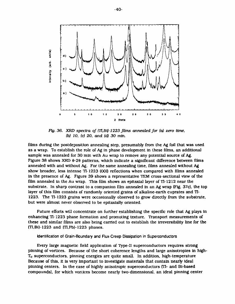
-40-
M
C
Cd
C
0 5 10 1 5 2 0 2 5 3 0 3 5 4 0
2 theta
Fig. 36. XRD spectra of (T1,B)-1223 films annealed for (a) zero time,(b) 10, (c) 20, and (d) 30 min.
films during the postdeposition annealing step, presumably from the Ag foil that was usedas a wrap. To establish the role of Ag in phase development in these films, an additionalsample was annealed for 30 min with Au wrap to remove any potential source of Ag.Figure 38 shows XRD 0-20 patterns, which indicate a significant difference between filmsannealed with and without Ag. For the same annealing time, films annealed without Agshow broader, less intense T1-1223 (001) reflections when compared with films annealedin the presence of Ag. Figure 39 shows a representative TEM cross-sectional view of thefilm annealed in the Au wrap. This film shows an epitaxial layer of T1-1212 near thesubstrate. In sharp contrast to a companion film annealed in an Ag wrap (Fig. 37c), the toplayer of this film consists of randomly oriented grains of alkaline-earth cuprates and T1-1223. The T1-1223 grains were occasionally observed to grow directly from the substrate,but were almost never observed to be epitaxially oriented.
Future efforts will concentrate on further establishing the specific role that Ag plays inenhancing T1-1223 phase formation and promoting texture. Transport measurements ofthese and similar films are also being carried out to establish the irreversibility line for the(Tl,Bi)-1223 and (T,Pb)-1223 phases.
Identification of Grain-Boundary and Flux-Creep Dissipation in Superconductors
Every large magnetic field application of Type-II superconductors requires strongpinning of vortices. Because of the short coherence lengths and large anisotropies in high-Tc superconductors, pinning energies are quite small. In addition, high-temperatureBecause of this, it is very important to investigate materials that contain nearly idealpinning centers. In the case of highly anisotropic superconductors (TI- and Bi-basedcompounds), for which vortices become nearly two-dimensional, an ideal pinning center
d)
:c)
b)
a)
. . . . . . . . . . . . . . . . . . . . . . .... . . . . . . . . . . . . v T I .R
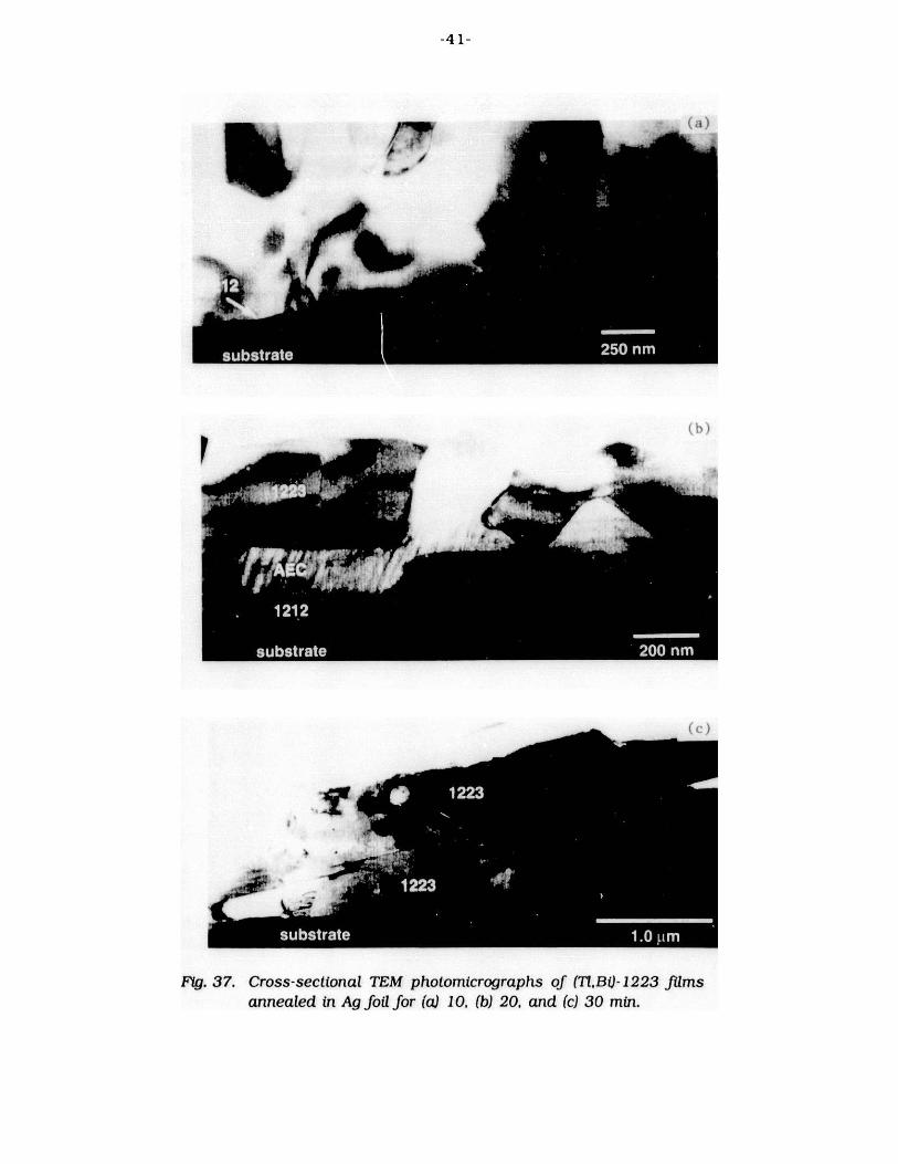
-41-
Fig. 37. Cross-sectional TEM photomicrographs of (TI,BI)-1223 filmsannealed in Ag foil for (a) 10, (b) 20, and (c) 30 min.

-42-
a
H
.0
0 5 1 0 1 5 2 0 2 5 3 0 3 5 4 0
2 theta
Fig. 38. XRD spectra for (TI,BO-1223 films annealed for 30 minand wrapped in either Ag or Au foil.
Fig. 39. Cross-sectional TEM photomicrograph of (T,BO-1223 filmsannealed in Au foil for 30 min.
introduces a pinning site in each and every superconducting layer. A columnar defectprovides such a pinning center. In addition, a convenient way to distinguish betweendissipation at grain boundaries and dissipation due to flux creep has been discoveredthrough studies of columnar defects. Inasmuch as ion-track pinning greatly increasespinning strength, it can expose the fingerprint of grain boundaries because ion trackssignificantly shift the I(V) characteristic (and therefore Jc) in weak-link free single crystalsand epitaxial films, but they have almost no effect on grain boundaries that are in serieswith transport current.
Ag wrap,30 min.
Au wrap,30 min.

-43-
Grain-boundary-free samples. We have measured I as a function of temperature,magnetic field, and defect density in 700 MeV Xe+ 42 ion-irradiated T2Ba2CaCu2Q8 films(from Superconductor Technologies, Inc.). In these samples, which are relatively free ofgrain boundaries, flux motion limits the current-carrying capacity. We found that, at hightemperatures when the vortex density is smaller than the areal density of columnardefects, the improvements in critical current with irradiation were substantial andrelatively independent of defect density. However, at fields for which the vorticesoutnumbered the defects, the improvements were significantly smaller.
The situation changed at lower temperatures, where the effect of the defects wasimportant in magnetic fields for which the vortex density was much larger than the arealdensity of defects. This finding emphasizes the importance of vortex/vortex interactionsin determining the critical currents at low temperatures. These points are demonstratedgraphically in Fig. 40.
Samples with grain boundaries. Samples with grain boundaries typically have smallerlow-field Jc and have I(V) characteristics that are qualitatively similar to those of aJosephson junction. Figure 41 is a plot of electric field E versus current density J or theE(J) of a polycrystalline material (from GE) and epitaxial samples of Ti-1223 (made by GEand ANL) measured at 77 K and 2 T. The nearly identical responses at low currentdensities suggest that, at this magnetic field and temperature, vortex motion dominatedthe dissipation. However, as the current was increased, there was a clear departure of thedissipation in the polycrystalline material from that measured in the epitaxial sample.This departure was attributed to phase slip at grain boundaries.
To further validate our interpretation of Fig. 41, we introduced columnar defectsthrough ion irradiation. These defects should only modify the dissipation that results fromvortex motion. Any changes in dissipation due to phase slip processes at grain boundarieswill be minimally affected through a loss in cross-sectional area available for transportcurrent. Therefore, comparisons of the transport properties of polycrystalline materialsbefore and after ion irradiation provide a way to separate the role of grain boundaries in theresulting dissipation. We have measured thick polycrystalline Tl-1224 films from GE,before and after irradiation. In Fig. 42, we plot the I(V) characteristic in both cases at 77 Kand 2 T. Clearly, the voltage measured at small currents, previously thought to be due toflux motion, was suppressed, whereas dissipation at high currents was relatively unchanged.
The described procedure provides the first definitive method to distinguish betweengrain boundary and flux creep dissipation. In the future, we plan to use the procedure tomake such identifications in various practical conductors, including PIT and thick-depositspecimens.
Effective Vortex Dimensionality and Pinning Force in Ion-Irradiated Samples
The effects of linear, ion-track pinning centers on dissipation and Je were investigatedin highly anisotropic TI-cuprate superconductors. For unirradiated and irradiated samplesat all fields, the dissipation accurately follows two-dimensional scaling. At intermediatefields, which rigorously follow such two-dimensional scaling without irradiation, theirradiated samples showed a dip in dissipation for fields parallel to the ion tracks. Thisseemingly contradictory behavior was explained as a balance between pinning and

-44-
-I I
106
10 5
10
10
102
101
100
10-110.1
\ Is..
I\ A
Sa
100
B (T)
Fig. 40.Jc vs. magnetic field B at varioustemperatures, before (opensymbols) and after (solidsymbols) ion irradiation: 40 K(triangles), 60 K (squares), and77 K (circles).
101
Fig. 41.Electric field vs. current density ofpolycrystalline (open symbols) andepitaxial (solid symbols) materials:e = voltage V/sample length, J =current I/cross-sectional area.
105
10-1
10-2
10-3
10-4
10
10
10-71C
10-3
10 -
10.1
N
E
a
\\ A
q
40 K Polycrystaillne4T
4 Epitaxal :
Fig. 42.Voltage vs. current for the samples inFIg. 41 before (open symbols) andafter (solid symbols) irradiation.Sharp reduction in dissipation atsmall currents in irradiated samplesuggests that dissipation in theregion is dominated by motion ofmagnetic flux..
b4-
010 '
10
10' -10-4
10
J (A/cm2)
77 K GE3572.OT TIBa:Ca:CuO,
-00aC
a . ..... .. . .I0
10 ' 10-2
I(A)
-
- -- - - -
N V I v w w w w w VI -
l l l l l l
r TT
U
.I
r
)3
--T-
lk

-45-
Josephson interlayer coupling energies. In addition, the effective pinning field of thedefects, for both dissipation and Jc, was clearly shown to be temperature dependent: itvanished at Tc and rose to roughly three to four times the effective ion-dose field at -0.4 Tc.
In conclusion, we have demonstrated the importance of vortex/vortex interactions atlow temperatures by taking advantage of available pinning centers.
2.3 Y-Ba-Cu-O Superconductors
2.3.1 Melt-Processed Y-123
Bulk Y-123 superconductors show promise in applications such as low-frictionsuperconductor/permanent magnet bearings and flywheel-energy-storage devices(Balachandran et al., 1994a). Melt-processing of Y- 123 is a well-established technique toproduce large-domain materials for levitation applications (Goretta et al., 1995a). Seedingwith higher melting Re 123 (Re: Sm, Nd) single crystals and use of well-defined temper-ature gradients are normally utilized to produce large single-domain levitators (Todt et al.,1995a). Alternatively, cube-shaped Nd1+,Ba2-xCu3 Oy seeds have been used to producefive-domain levitators (Todt et al., 1995b-d). Microstructural investigation of the five-domain materials revealed that these levitators are composed of five domains that arerotated 90 around a common [1001/10101 axis, relative to their neighboring domains.The levitation forces of the five-domain materials can be comparable to those of single-domain materials, but they show a much wider fluctuation of levitation force than single-domain materials.
To understand the high levitation forces, as well as the large fluctuations, detailedinvestigations of the microstructure have been carried out. Transmission electronmicroscopy revealed the existence of several special kinds of 900 grain boundaries. Puresymmetrical-tilt boundaries have been observed, as well as tilt boundaries parallel to the abplane of one of the neighboring domains. Pure 900 twist grain boundaries have also beenobserved (Fig. 43). Reports indicate that this type of grain boundary can carry very high Jevalues in thin films (Eom et al., 1991). Preliminary measurements on our bulk materialssupport this result.
Extensive cracking of many samples may be responsible for large fluctuations inlevitation force. Thermal cycling experiments with single- and five-domain levitatorsshowed a decreasing levitation force with an increasing number of thermal cycles for thefive-domain levitator, whereas this dependence was much weaker for the single-domainlevitators (Todt et al., 1995c). This finding indicates that thermal cycling damages thealready cracked five-domain samples even more, thereby decreasing the well-connectedareas in the sample. Single-domain samples exhibit cracking in the ab planes only, and thecracks do not propagate with cycling; therefore, no decrease in levitation force occurs.
2.3.2 Grain-Boundary Transport and Microstructure
To better quantify conduction across weak-link grain boundaries in superconductors,we have measured microstructure and transport on 240 [0011-tilt bicrystal grain boundariesin Y-123.

-46-
Fig. 43. TEM photomicrograph of 90 twist boundary in melt-processedY-123.
Single grain boundaries were prepared by epitaxial growth of Y-123 onto bicrystallineSrT103 substrates. Microstructural characterization by TEM showed that these artificiallyinduced grain boundaries were periodically decorated by impurity phases. In addition, theboundaries were not always straight, but instead, frequently meandered away from the path
of the underlying boundary in the substrate. The various facets produced by the mean-dering showed varying degrees of tilt and twists. Atomic-force microscopy studiessuggested that this meandering behavior is related to the nucleation and growthmechanisms of the film, and based on this, we were able to vary the magnitude of themeandering by changing the growth conditions.
In addition, we measured the zero-field electrical transport properties and foundthem to be in excellent agreement with the Ambegaokar-Halperin model over an extendedrange of currents and voltages. This model gives a firm basis for characterizing andcomparing boundaries, and provides two independent measures of the grain boundarycritical current: these are found to differ significantly from each other. The differenceprovided new evidence that the boundary is not uniform, but composed of a number ofsmall Junctions in parallel. The implied junction size is consistent with gross defectsfound in TEM photomicrographs of such boundaries.

-47-
2.4 Properties of Bulk High-Tc Superconductors
2.4.1 Characterization Methods
Ceramic superconductor samples produced in ANL projects are characterized to helpimprove chemical formulations and forming and processing procedures. High-Ta productsfabricated for devices also are characterized to evaluate product performance. The prop-erty of primary interest is DC transport critical current of the sample, measured as afunction of intensity of an applied magnetic field. Power loss due to AC transport, as afunction of frequency, current, temperature, and ambient magnetic field, is of interest forAC applications also. Selected samples are tested to find critical temperature, structuraldefects, strength of the diamagnetic response, remanent-field strength, and mechanicalproperties (Balachandran et al., 1994a). Thermal conductivity of sinter-forged Bi-2223current leads through the 4-77 K temperature range are also obtained.
2.4.2 Electrical Characterization of Superconductors
DC Characterization
Critical current tests have continued at an average rate of 103 samples per month.Substantial differences among batches of bulk material or formed products required
continual screening. The standard four-point resistance method was used with a 1 sV/cmcriterion. Sample types consisted primarily of Ag-clad Bi-2223 tapes that were underdevelopment for magnetic coil applications and Y- 123/Ag or Bi-2223 bars that were beingdeveloped for use in current leads. Results are discussed below and elsewhere in thisreport.
Tests of high-performance superconductors at high currents during this reportingperiod were supported by our pulsed-current facility, now upgraded to provide 1600-Apulses. Tapes were tested at 77 K individually in a low range, typically 10-40 A, and in
parallel assemblies at currents to 1500 A. Individual Bi-2223 sinter-forged bars with 0.5-0.6 cm2 cross-sectional areas and critical currents to 710 A were tested at 77 K throughand beyond their critical values. Applied magnetic fields typical of current lead applica-tions (50-100 G) decreased critical current negligibly.
AC Power-Loss Study
A small resistance to AC flow is displayed by high-Ta superconductors, even at currentswell below the DC critical current. This resistance is associated with the magnetic hys-teresis of the material. However, appropriate design can limit the power loss to a valuesufficiently small for advantageous use of the material in applications such as AC downlinksoperated at power-line frequencies (Balachandran et al., 1995a). AC losses in supercon-ductor bars and tapes that are potentially useful in AC devices are being evaluated insupport of design efforts. Typical results from sinter-forged Bi-2223 bars were shown inthe previous report (Balachandran et al., 1994a). Studies of the effects of sample shape,ambient AC magnetic field, and current distribution in arrays of parallel samples continue.
Figures 44 and 45 show newly constructed apparatuses that support the AC power-lossstudies. A multicontact fixture (Fig. 44) enables differential AC voltage measurements atseveral sites along both broad and edge surfaces of a rectangular bar specimen during a

-48-
.0 40 4 4 40 4 A
Fig. 44. Multicontact fixture for differential AC voltage measure-ments at several sites on superconductor bar; inductivepickup loops are incorporated to monitor local currentflow.
single session of cryogenic testing. Inductive pickup loops are incorporated to measurelocal current flow. The fixture can be used on a specimen tested singly or as part of anarray. The parallel-bar fixture (Fig. 45), which accepts up to eight samples and can beadjusted over a large range of sample lengths, provides a current-metering facility for eachsample. The fixtures are used with a variable-frequency AC source capable of deliveringup to 2150 A RMS sine waves to test an assembly being developed for power utility serviceat 2000 A RMS.
Contact Resistivity
Low-resistance contacts (Maroni 1991, 1992) are needed for DC and AC applications.Resistance to 50-Hz AC flow through Ag contacts sintered to high-Tc superconductors wasmeasured with samples at 77 K and was compared with the resistance to DC flow. The ACresistance of such contacts at 4.2 K also was measured. A lap-joint sample configurationwas used for all measurements of contact resistance. Sample lap area was 0.64 cm2 forY-123/Ag bars and 1.17 cm 2 for Bi-2223 bars. AC resistance was corrected for the rela-tively small contributions from the bulk high-Tc material included in the monitored lengthof each joint. The tests were done to aid interpretation of results from downlink heat-leakstudies in which the question of large differences between AC and DC resistance, even inthe current range <10% Ic, had been raised.
Half-joint resistivities in 77-K tests were 0.1 mW-cm 2 and 0.2 mW-cm 2 for Y-123/Agand Bi-2223, respectively. Values with AC were nearly the same as with DC. The valuesinclude contributions from the Ag/ceramic interface, the Ag metal thickness, and a
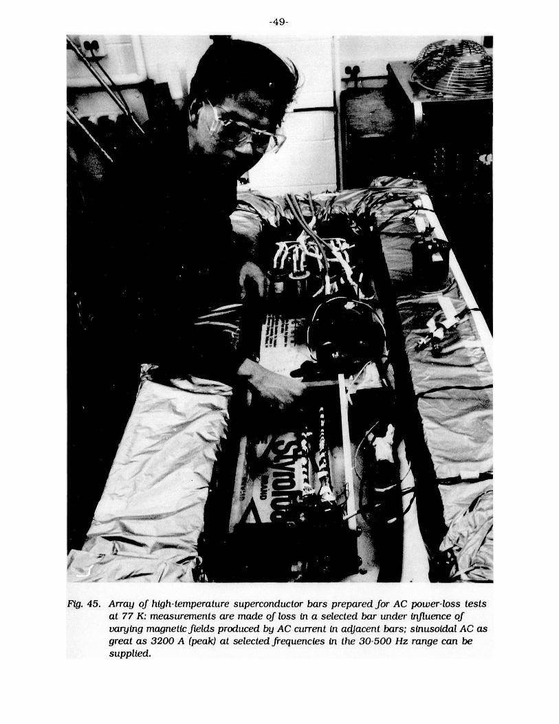
-49-
Yr 7i
I
r j. i
L
.,4I
/ (-f"
Ii
Fig. 45. Array of high-temperature superconductor bars prepared for AC power-loss testsat 77 K: measurements are made of loss in a selected bar under influence of
varying magnetic fields produced by AC current in adjacent bars; sinusoidal AC asgreat as 3200 A (peak) at selected frequencies in the 30-500 Hz range can besupplied.
i
r
t MoowYl IRf
t
. .. .r
-50-
minimal amount of Sn-Pb solder used to join the bars. At 4.2 K, the Bi-2223 AC value foundwas too small (19 nW-cm2 ) to contribute substantially to heat-leak totals in the downlinkstudies. Tests of high-Tc/low-Tc joints at 4.2 K are being prepared.
Electrical-Cycling Tests
Long-term electrical-cycling tests of high-Tc bar samples produced by ANL wereconducted jointly with ERIEZ Magnetics Technical Center of Erie, PA (ERIEZ). A set offive Y- 123/Ag bars with critical current values from 99 to 129 A in 77-K tests were treatedwith spray wax, retested, and sent to ERIEZ for electrical cycling at 77 K, similar to thatexpected in possible application as downlinks in a magnetic separator. Three bars wereenergized to 23-24 A DC for 30 s once every 60 s until 104,000 such cycles had beenapplied, while two bars served as nonenergized controls in the same environment.The critical current values were monitored by ERIEZ during this treatment and by ANLafterwards. The finding of both laboratories was the same; no detrimental effect on thecritical currents occurred from the electrical cycling or from any other cause in either testbars or controls during the year between ANL tests, during which the ERIEZ electricaltreatments were applied. The absence of any effect of atmospheric exposure and time waslikely due to isolation by the thin wax coating. Also, the wax and its carrier were shown toexert no detrimental effect. In contrast, during storage in plastic bags for several monthsbefore selection for use in this test, nonwaxed bars lost 10-28 % of their original criticalcurrent values.
Cooperative work was continued with the test of a Bi-2223 bar that was sinterforged at ANL and cycled electrically at 77 K at ERIEZ. The 565-A critical current (J_ =1200 A/cm2 ) was not significantly changed by 80,000 pulses at 50 A on a 30-s-on, 30-s-offschedule. The bar was coated with Krylon "anti-rust" spray wax before the cyclingtreatment. Again, there was no detrimental effect of waxing or elapsed time between tests(3 months). Also, the bar performance had not deteriorated in 4 months of storage beforewaxing, during which time the bar was protected by forged-on Ag foil that was removed for
the subject test.
Material from a longitudinally sectioned, sinter-forged bar was pulse-tested at a seriesof temperatures below 77 K and in applied magnetic fields up to 1 T. A small slopechange in Je vs. T at 30-35 K when applied magnetic fields were present may indicateimproved flux pinning below that temperature range. At zero applied field, the ratio ofcritical currents at 4 and 77 K was =6.
Pulsed DC tests were performed to evaluate candidate conductors for use as currentdownlinks in an SMES application. Superconductor bars made by ASC had been formed byaligning Bi-2223/Ag-Au tapes and sintering them together to make downlink elementsrated at 1100 A in a 60-4 K temperature gradient with <0.4 W of heat leak per 50-cm-longbar. After tests showed that these criteria had been met, the bars were sectioned forfurther study. Nearly 1500 A DC were needed to reach the critical values of some of the
segments.
2.4.3 Thermal Conductivity Measurements
Sinter-forged Bi-2223 bars are being applied in current leads that connect electriccurrent through a 77-4 K temperature gradient to devices operating in liquid He. Therelatively low thermal conductivity of the ceramic and its electrical superconductivity
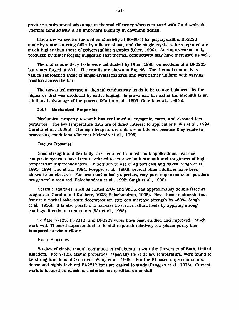
-51-
produce a substantial advantage in thermal efficiency when compared with Cu downleads.Thermal conductivity is an important quantity in downlink design.
Literature values for thermal conductivity at 60-80 K for polycrystalline Bi-2223made by static sintering differ by a factor of two, and the single-crystal values reported aremuch higher than those of polycrystalline samples (Uher, 1990). An improvement in Jcproduced by sinter forging suggested that thermal conductivity may have increased as well.
Thermal conductivity tests were conducted by Uher (1990) on sections of a Bi-2223bar sinter forged at ANL. The results are shown in Fig. 46. The thermal conductivityvalues approached those of single-crystal material and were rather uniform with varyingposition across the bar.
The unwanted increase in thermal conductivity tends to be counterbalanced by thehigher Je that was produced by sinter forging. Improvement in mechanical strength is anadditional advantage of the process (Martin et al., 1993; Goretta et al., 1995a).
2.4.4 Mechanical Properties
Mechanical-property research has continued at cryogenic, room, and elevated tem-peratures. The low-temperature data are of direct interest to applications (Wu et al., 1994;Goretta et al., 1995b). The high-temperature data are of interest because they relate toprocessing conditions (Jimenez-Melendo et al., 1995).
Fracture Properties
Good strength and flexibility are required in most bulk applications. Variouscomposite systems have been developed to improve both strength and toughness of high-temperature superconductors. In addition to use of Ag particles and flakes (Singh et al.,1993, 1994; Joo et al., 1994: Poeppel et al., 1993), several other additives have beenshown to be effective. For best mechanical properties, very pure superconductor powdersare generally required (Balachandran et al., 1992; Singh et al., 1995).
Ceramic additives, such as coated ZrO2 and SnO2, can approximately double fracturetoughness (Goretta and Kullberg, 1993; Balachandran, 1995). Novel heat treatments thatfeature a partial solid-state decomposition step can increase strength by -50% (Singhet al., 1995). It is also possible to increase in-service failure loads by applying strongcoatings directly on conductors (Wu et al., 1995).
To date, Y-123, Bi-2212, and BI-2223 wires have been studied and improved. Muchwork with TI-based superconductors is still required; relatively low phase purity hashampered previous efforts.
Elastic Properties
Studies of elastic moduli continued in collaborati. a with the University of Bath, UnitedKingdom. For Y- 123, elastic properties, especially th 4e at low temperature, were found tobe strong functions of 0 content (Wang et al., 1995). For the Bi-based superconductors,dense and highly textured Bi-2212 bars are easiest to study (Fanggao et al., 1993). Currentwork is focused on effects of materials composition on module.
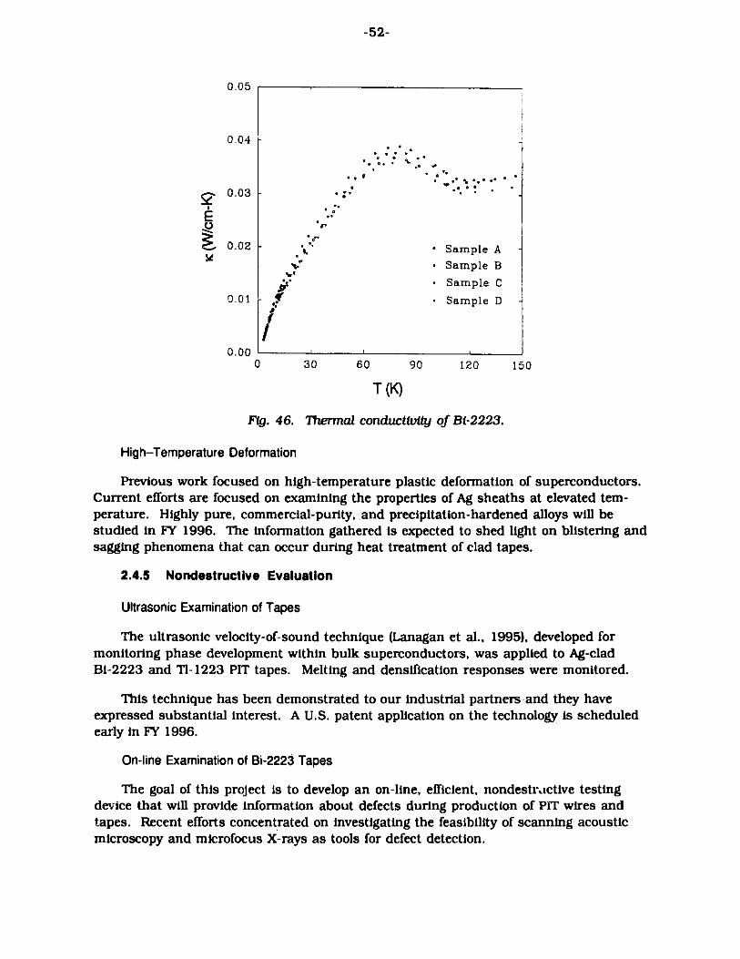
-52-
0.05
0.04
0.-1S m B
" se
5...
0.02 01VV. Sample A
0"Sample C
0.01 - .Sample D
0.000 30 60 90 120 150
T (K)
FIg. 46. Thermal conductivity of Bi-2223.
High-Temperature Deformation
Previous work focused on high-temperature plastic deformation of superconductors.Current efforts are focused on examining the properties of Ag sheaths at elevated tem-perature. Highly pure, commercial-purity, and precipitation-hardened alloys will bestudied in FY 1996. The information gathered is expected to shed light on blistering andsagging phenomena that can occur during heat treatment of clad tapes.
2.4.5 Nondestructive Evaluation
Ultrasonic Examination of Tapes
The ultrasonic velocity-of-sound technique (Lanagan et al., 1995), developed formonitoring phase development within bulk superconductors, was applied to Ag-cladBi-2223 and T1-1223 PIT tapes. Melting and densification responses were monitored.
This technique has been demonstrated to our industrial partners-and they haveexpressed substantial interest. A U.S. patent application on the technology is scheduledearly in FY 1996.
On-line Examination of Bi-2223 Tapes
The goal of this project is to develop an on-line, efficient, nondestructive testingdevice that will provide information about defects during production of PT wires andtapes. Recent efforts concentrated on investigating the feasibility of scanning acousticmicroscopy and microfocus X-rays as tools for defect detection.

-53-
In the process of producing thin, clad tapes, the internal powder core can developthickness variations (sausaging) that degrade performance. An on-line nondestructivetesting device to provide information on sausaging and other defects in as-produced tapesis very much needed. Two nondestructive methods that are potentially capable of moni-toring the production of defect-free superconducting tapes have been examined. Ag-cladBi-2223 tapes =250 m thick were used.
Acoustic microscopy. The nondestructive characterization of the tapes was conductedat Sonoscan Inc., Bensenville, IL. The work was performed under a-CRADA. Acousticmicroscopy may offer an excellent way of imaging the powder within the tube. Thesamples are relatively thin and can be immersed in an acoustic coupling medium such aswater. A simplified block diagram of the setup is shown in Fig. 47. Because the samplesare thin (core =75 pm), the focus is essentially though the entire thickness of the sample.Acoustic pulses travel forward and back through the tape, and are detected by the sendingtransducer, which is operated in a pulse-echo mode. Results are displayed as a gray-scaleimage, in which the shade of gray can be related to features in the tape. The image canalso be displayed in color. Work is continuing in collaboration with Sonoscan.
Microfocus X-rays. Ag-clad Bi-2223 tapes were also studied with ANL's microfocusX-ray system (Fig. 48). This system consists of an X-ray source and a detector comprising a14-bit CCD camera and an image intensifier. The X-ray source is a microfocus system, witha spot size of on 10 pm, a tungsten target, and a maximum energy level of 160 kVp at0.15 mA. The system is controlled by a computer, which also stores the raw image data.
Bi-2223 tapes were mounted in air to prevent any masking effects of solid mountingmaterial. The tapes were aligned in front of the intensifier, and the image was projectedonto the intensifier screen. The image was captured live through a digital CCD camera(filmless radiography).
Moon
Controllers
Pulser-
Receiver
AmpfGate 1 Host Computer
CRT Hard-CopyOscilloscope Image Image
aXYZ Motion
Transducer
Sample
FIg. 47. Block diagram of acoustic microscopy setup for nondestructivecharacterization of Bi-2223 tapes.

-54-
Microfocus CCD CameraX-Ray Tube
Ribbon Image Intensifer Fig. 48.Schematic diagram of ANL micro-
focus X-ray system.
Mirror
Sample Stage
Motion Control & Image ProcessingData Acquisition & Display
Preliminary results indicate that acoustic microscopy is feasible for examiningsuperconducting tapes. Figure 49 shows the acoustic microscopy images of four tapes.The outside white region is the Ag tubing. The superconducting core is shown as thedarker gray inner region of the image. Lighter regions represent low acoustic attenuationregions, and the dark regions indicate high attenuation. The dark and bright striations onthe image represent density variations in the packed powder. The image clearly showsthat the powder is not uniformly distributed inside the tape, which is known to be one ofthe causes of poor properties.
X-ray images of the same tapes are shown in Fig. 50. The scale factors of the acousticpictures, and the X-ray pictures are. different, which makes point-by-point comparisondifficult. However, there is general agreement between. the images on the nonuniformity ofpowder density. On the X-ray images, the dark gray regions represent low X-ray attenu-ation, and the white region corresponds to high attenuation. The outer darker region onthe images represents Ag tubing, and the inner core shows dark and bright shades,depending on the local attenuation. Once again, these images confirm the nonuniformdensity of the powder in the Ag tube.
In future work, a second set of controlled sample tapes with different rollingreductions will be examined. We expect to obtain better correlation for the new set ofcontrolled samples, when compared with the preliminary samples used in the presentstudy. An additional set of controlled samples with various degrees of mechanical strain isnow being prepared. In particular, we are interested in the formation of voids as a result ofmechanical strain. All of the new samples will also be investigated by optical and SEM andthe observations will be .correlated with the results from the nondestructive imagingmethods.

-55-
The outer silver tubing
ti5
T'hIie inside powder core
The outer silver tubiIA \
5
mm
mm
Ihe inside powder core
FIg. 49. Acoustic microscopy images of Bi-2223 tapes.
Magneto-optical imaging
Ag-clad Bi-2223 tapes have been provided to the staff of ANL's Materials Science Divisionfor use in magneto-optical imaging studies, which have led to direct imaging of high- andlow-current paths in the Bi-2223 core. These observations have been correlated withdetailed electron microscopy (Welp et al., 1994, 1995) and are now being used to guideimprovements in tape processing.
2.5 Applications and Devices
Application research and development are focused on production and testing ofcomponents, analysis of performance (Cha et al., 1994b; Hull et al., 1995), and design of
new systems. Primary emphasis has been on current leads and magnetic bearings.
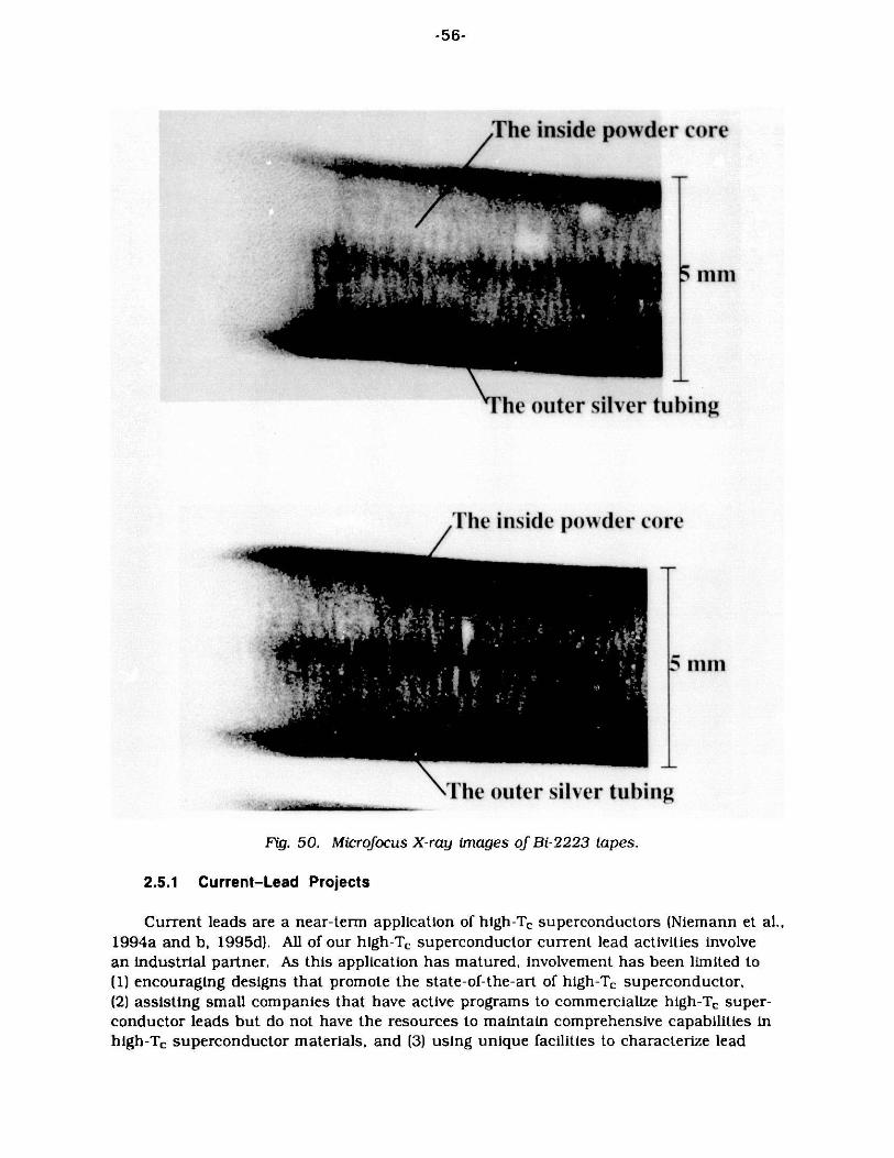
-56-
The inside powder core
nm
The outer silver tubing
The inside powder core
1 11111
The outer silver tubing
Fig. 50. Microfocus X-ray images of Bi-2223 tapes.
2.5.1 Current-Lead Projects
Current leads are a near-term application of high-Tc superconductors (Niemann et al.,
1994a and b, 1995d). All of our high-T superconductor current lead activities involvean industrial partner. As this application has matured, involvement has been limited to(1) encouraging designs that promote the state-of-the-art of high-Ta superconductor,(2) assisting small companies that have active programs to commercialize high-T super-conductor leads but do not have the resources to maintain comprehensive capabilities inhigh-Ta superconductor materials, and (3) using unique facilities to characterize lead
,., . .R_
.q ley X . .;
. _. _. .

-57-
performance so that these facilities need not be duplicated by companies with limitedresources (Cha et al., 1995a,b). In all of the collaborations, the preference is to constructleads with commercially available high-Ta superconductor materials.
Superconductivity, Inc., Leads
An ongoing superconductor current lead project is a collaboration with Superconduc-tivity, Inc., to develop a 1500-A high-Ta superconductor lead (Fig. 51) for use in a power-quality control SMES system. Staff from the company have participated in all stages of theproject. Technical progress in FY 1995 has consisted of evaluating the performance ofcomponents and leads. A key component in the project has been the development of aheat intercept at the warm end of a high-Ta superconductor that has a very high electricalresistivity (electrical isolation) but a low thermal resistivity (heat transfer). Such inter-
cepts are necessary features for high-Ta superconductor leads if their performance is to besubstantially better than conventional, vapor-cooled Cu leads (Niemann et al., 1995e).
The leads, constructed in FY 1994, have been installed in a performance-evaluationcryostat and instrumented. The leads have been cooled to operating temperature and havebeen operated to 1150 A during measurement system checkout (Niemann et al., 1995a andb). Joint technology development efforts with Superconductivity, Inc., include currentlead design methodologies, which include performance, safety, reliability, and cost;intermediate-temperature heat intercepts with low heat transfer and high voltage isolation;and demountable screw-type electrical connections.
A follow-on program has been initiated for the purpose of designing second-generation1500-A high-Ta superconductor current leads and performing associated conductorburnout evaluations. Conceptual lead design is underway and burnout analysis has beeninitiated. Figure 52 indicates the predicted burnout: i.e., burnout time for a 0.5-cm-diameter x 15-cm-long Bi-2212 rod with initial cold and warm end temperatures of 4 Kand 77 K, respectively, when Tmax = 300 K.. At 77 K, the Je below which the conductor isin perfect superconducting state, is 1747 A/cm2 . Therefore, if the operating currentdensity is less than the Jc, there is no heat generation. For a 400-A operating current, thecurrent density becomes 2037 A/cm2 , which is greater than the Jc and there will begeneration of flux-flow resistivity heat. The temperature change is concentrated near thewarm end. Initially, the temperature rise is very slow because the low flux-flow resistivityis low. However, when the maximum temperature reaches the critical temperature
(Tcrit = 90 K), the portion of the rod where the temperature is greater than the criticaltemperature becomes normal. The normal-state resistivity is much greater than the flux-flow resistivity. The maximum temperature of the rod reaches burnout temperature,i.e., 300 K, very quickly after the maximum temperature reaches critical temperature.By numerical calculation, the burnout time is 2.9 s. Burnout test apparatus to verify theperformance predictions is under construction. We plan to evaluate the burnoutcharacteristics of both bulk and PIT conductors.
Babcock & Wilcox Leads
In a collaborative project with Babcock & Wilcox, a 16-kA high-Te superconductor leadfor use in an 0.5 MWh SMES device is being developed. Features of the design include aconduction-cooled high-Te superconductor stage and use of multiple elements of PIT Bi-2223 with an Ag/3% Au sheath embedded in a stainless steel safety lead (Niemann et al.,

-58-
Fig. 51.
Superconductivity, Inc., current leadprior to installation in performance-evaluation cryostat; six parallel YBCOw/15% Ag high-T superconductor rodsand a thermally effective, electricallyisolating heat intercept assembly areincorporated.
"IL.,
100
1=400 A
95 P - nem 2.9 sec
90 r 2.8
r 285 -
. 80
0. 2
75 0-
700.13 0.134 0.138 0.142 0.146 0.15
x (m)
Fig. 52. Burnout time prediction for Bi-2212 rod.

-59-
1995a, 1995c). Work included design of the lead, evaluation of vendor-supplied high-Tcsuperconductor elements, construction of a prototype lead, and initiation of constructionof a lead assembly. Staff from the company are involved in all stages of the development,including construction of the lead.
The high-Tc superconductor element consists of a composite sintered stack of cladtapes (Fig. 53). Eighteen conductor elements are mounted in parallel in a safety leadassembly (Fig. 54). A prototype lead assembly was built to develop manufacturing methods,quality verification, and assembly procedures. The prototype safety lead is shown inFig. 55.
Two preproduction samples of conductor elements intended for use in the currentlead assembly have been evaluated under anticipated use conditions. The conductorelements were manufactured by ASC. Critical current at 77 K in self field with a 1-mV/cmcriterion was measured at ASC in a DC mode and at ANL in a pulsed-current mode. Thecritical current values measured in the DC mode were somewhat lower than thosemeasured in the pulsed-current mode, most likely because of resistive heating of normalmetal contacts. Critical current at 60 K and B//b and B//c was measured in a pulsed-current mode. Typical results for one of the samples are shown in Fig. 56. One sampleconductor element was subjected to 50 295-K .E 77-K A 295-K thermal cycles with nosignificant change in critical current. One sample conductor element was subjected to 600electrical ramp cycles, corresponding to those predicted for the SMES current leadapplication, with no significant change in critical current.
Specific resistivities of metallic contacts to the superconductive cores of tape samples,comparable to those used in the composite bars, were measured. Half-joint resistivities at77 K ranged from 0.031 to 0.037 Q-cm2 . Lap-joint resistivity tests were performed withspecially formed Ag metal connectors sintered to the tapes. The average resistivity of thehalf joints at 77 K, including the contribution from the Ag connector and its sinteredinterface to the tapes, was =1 p S-cm 2. The irreversible strain limit of both sampleconductor elements was 0.2%, and retained critical current was >90% (Fig. 57). Thesample conductor elements displayed a high degree of structural and electrical integritywith no noticeable performance degradation despite being handled many times by variousindividuals.
In FY 1996, a test of a single high-Te superconductor lead assembly under theanticipated operating conditions of the SMES magnet will be conducted at the NationalHigh Field Magnet Laboratory. Current lead performance evaluations include conventionalupper-stage heat leak, mass flow and temperature optimization, integrated assembly rampto 17,600 A when B = 0.2 T, optimization of mass flow and temperature at 16,000 A whenB = 0.2 T, and determination of heat leak. Reliability evaluations include thermal cycles,electrical cycles, and safety lead function.
Joint technology development with Babcock & Wilcox included design methodologiesthat include performance, safety, reliability, and cost; demountable screw-type electricalconnections; design and fabrication of PIT tape composite conductors with ASC to give aconductor with specified performance along with structural integrity and the dimensionalprecision required for straightforward construction of multielement current lead assemblies.

-60-
Irirw( '))IYI' III' I N)
COL) [ND 4.8mm(.182") WARM END
.034(.9mm)TYP. THIS END
6.6rmff( 260") 6.4mm(.25')
30mnm(1.18" )- -
--- 30mm(1.18" )
03/32 DOIl L X .25 DEEP - 540mm(21.25")--
14.rm(.580") A B4rr( 015") 10.7mm(.420") .4mm(.015")
i TYP.
12.1mm(.478")
18.4rnrn(.124") 1.9mm(.073")
- - .%4nrr(. 1$4") A BPIT TAPES
-- -- .tirrrr(.2(i/') END CAP
SILVER (Ag) BLOCK
0 10 50 100SCALE. IN rnm SECTION A-A SECTION B-B
SCALE: 2X SCALE: 2X
FINALHTS CONDUCTOR ELEMENT
Fig. 53. Babcock & Wilcox high-Tc superconductor: geometry of elements.
American Superconductor Corporation Leads
High-current composite conductor elements from ASC will be electrically charac-terized at 60 K. The characterization will provide a correlation with performance at 77 K,which is readily measured by ASC. This correlation will be an important factor in thedesign of future high-current high-Ta superconductor leads.
Critical current will be measured in the ANL facility that consists of a variable-temperature He cryostat, a superconducting magnet, and a current pulser. The variable-temperature cryostat is configured to contain two samples and will be rotated in themagnet to provide B//b and B//c applied-field orientations. The magnet provides a high-homogeneity, large-volume field, with magnitudes to 2.5 T. The superconducting magnetand variable-temperature cryostat are shown in Fig. 58.
ZerRes Corporation Leads
As part of a collaborative agreement with ZerRes Corporation (ZerRes), ANL hasconducted experiments to measure the critical currents of a high-Tc superconductorcurrent lead supplied by ZerRes under various thermal and magnetic field conditions.The composite leads are manufactured by a proprietary process developed by ZerRes(Zimmerman et al., 1993).

-61-
LTS CAHLE (18) H ELESAFETY LEAD
\ C
COLD-END
CI D-I ND CLAMPED CONNEC
WARM-END SCREWED CONNECTION
HEAT INTERCEPT GAS INLET -
CURRENT BUS
MENT (18)
CURRENT COLLECTOR
TION
WARM-END CURRENT DISTRIBUTOR
u 10 50 100'AL[ IN mm
Fig. 54. Babcock & Wilcox middle-stage (60-K A 5-K) current lead assembly. Eighteenconductor elements in parallel carry a current of 16,000 A. A stainless steel safetylead provides an alternate current path and thermal stabilization for the high-Tesuperconductor elements.
Fig. 55. Babcock & Wilcox prototype safety lead assembly.

-62-
100 '-
B [TJ 8//co 0.02
80 0 0.060 0.07" 0.08 Fig. 56.
60 - 0.09 Voltage drop vs. current at0.10 60 K and B//c (250-mm
electrode gap) of a Babcock40 ~& Wilcox conductor element.
20
00
900 950 1000 1050 1100 1150 1200
1 (A)
1.2 .
1Fig. 57.
0.8 Variation of retained Ic
fraction with axial strain ofBabcock & Wilcox element.
0.6-
0.4
0.2
0 1 2 3 4 5
Strain
The experimental apparatus includes an R & A magnet, a measurement cryostat, aninsert, and the instrumentation systems. The insert includes primarily the current lead,the temperature sensors, the voltage taps, and three resistive heaters. The lead is housedin an epoxy/fiberglass composite tube with brass caps on both ends. Two silicon diodeswere installed on the brass caps to measure the temperature at the upper and lower endsof the current lead. Two voltage taps were soldered to the Cu wires on both ends of thelead to measure the voltage drop across the lead. Two heaters were mounted on the brasscaps of the lead for temperature control. A third heater was installed near the bottom ofthe cryostat in case more boiloff was needed for temperature control. The entire insertassembly also included a liquid-He-level sensor and a current return path (a Cu wire) forthe lead. By adjusting the current through the heaters and the liquid He level in thecryostat, the desired temperatures and temperature gradients were obtained.

-63-
Fig. 58.
Superconducting magnet andvariable-temperature cryostat in
ANLfacility for measuring Ic.
Critical current was tested by pulsing a constant current through the lead and
observing the corresponding voltage drop across the lead. The battery-powered currentsupply was driven by a ground-isolated wave function generator. The desired current wasobtained by adjusting the amplitude of the generator output. Current-pulse duration wasfixed at 200 ms for all tests reported here. The shape and magnitude of the current pulsewere monitored and stored on a ground-isolated oscilloscope. Output from the voltage tapswas fed into a differential preamplifier and displayed and stored on another oscilloscope.
Two types of tests, isothermal and thermal gradient, were performed. Isothermal
tests were carried out at 5.4, 21, and 59 K. Two temperature gradient tests, 20-60 K and5-70 K, were conducted. For each test, the lead was subjected to a constant applied fieldof 0, 260, 520, and 1040 G. Each test is begun by adjusting the currents through the twoheaters and the liquid He level in the cryostat. Once the specified temperature or temper-
ature gradient is reached, voltage-vs.-current measurement commences. Current isgradually increased until either the voltage drop becomes too large or the thermal runawaycondition is reached. Thermal runaway is the effect of internal heating in the lead as aresult of dissipation in the superconductor. More information on dissipation and thermalrunaway can be found in Askew et al. (1993). In addition, tests at liquid N 2 temperaturewere conducted with a different setup. The applied fields for the liquid N2 tests were 0and 55 G.
-64-
Figures 59-61 show the voltage-vs.-current (V/I) characteristics of the ZerRes lead atvarious temperatures and applied fields. The effect of the applied magnetic field on thecritical current of the lead is evident from these figures. Figure 62 shows the V/I charac-teristics at different temperatures with zero applied field. As expected, critical currentdecreases with increasing temperature. In general, the lowest critical current for a givenapplied field is associated with the 5-70 K gradient test, followed by the isothermal test at60 K. The only exception is that at zero applied field, the critical currents for the 20-60 Kand the 5-70 K gradient tests are smaller than that at 77 K. This abnormal behavior isprobably not real and can likely be attributed to the fact that the temperature in the leadhas not reached the steady-state conditions under zero applied field. The two temperaturegradient tests at zero applied field begin immediately after the temperature at both ends ofthe lead reached specified values. Because the thermal conductivity of the high-Tc super-conductor lead is relatively poor, the temperatures along the lead are not likely to havereached steady state in such a short period of time. Subsequent tests at nonzero appliedfield did not show this abnormal behavior because these tests were always conducted afterthe zero field tests and there was sufficient time for the lead to reach steady state.
H, gauss-o 0 -A 260o 520 -x 1040
0 -
0 .0
0-
)
20 40 60Current (A)
0 20 40 60Current (A)
Fig. 59.Voltage-vs. -currentcharacteristics of ZerReslead at various appliedfields for T = 21 K.
80 100
Fig. 60.Voltage-vs. -currentcharacteristics of ZerReslead at various appliedfields for T = 59 K.
80 100
12000
10000 x
800017
6000 ./
04000
2000
- x- X
-x- xo
IU
0
A 0
12000
10000
8000
6000
4000
2000
A
:.t:a)
*n
0
- H, gauss0 0 0
- A 260x A 520
- x 1040 00 0
-x-0
-0
Aoc9~?V
S.
. . . . . . . . . . . . .
VLvLWiAJ6ilV
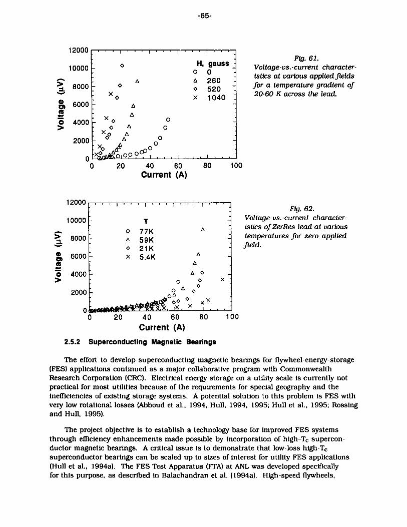
-65-
12000
0 H, gaussV Fg. 61.
100000 0 Voltage-vs.-current character-
s A 260 istics at various applied fields
3 8000 - 0 520 for a temperature gradient of
x o x 1040 20-60 K across the lead.
v6000 -A
o 4000 0>1 xo A 0
2000 000
0 5*aooo9*i .
0 20 40 60 80 100Current (A)
12000Fig. 62.
10000 T Voltage-vs. -current character-8istics of ZerRes lead at various
>- o 77K
8000 59K temperatures for zero applied0 21K .field.
6000 x 5.4K A
o 4000- e 0>1 0 0 x
0
2000- 0 0
0 X0 20 40 60 80 100
Current (A)
2.5.2 Superconducting Magnetic Bearings
The effort to develop superconducting magnetic bearings for flywheel-energy-storage(FES) applications continued as a major collaborative program with CommonwealthResearch Corporation (CRC). Electrical energy storage on a utility scale is currently notpractical for most utilities because of the requirements for special geography and the
inefficiencies of existing storage systems. A potential solution to this problem is FES withvery low rotational losses (Abboud et al., 1994, Hull, 1994, 1995; Hull et al., 1995: Rossing
and Hull, 1995).
The project objective is to establish a technology base for improved FES systems
through efficiency enhancements made possible by incorporation of high-Tc supercon-ductor magnetic bearings. A critical issue is to demonstrate that low-loss high-Tasuperconductor bearings can be scaled up to sizes of interest for utility FES applications(Hull et al., 1994a). The FES Test Apparatus (FTA) at ANL was developed specificallyfor this purpose, as described in Balachandran et al. (1994a). High-speed flywheels,
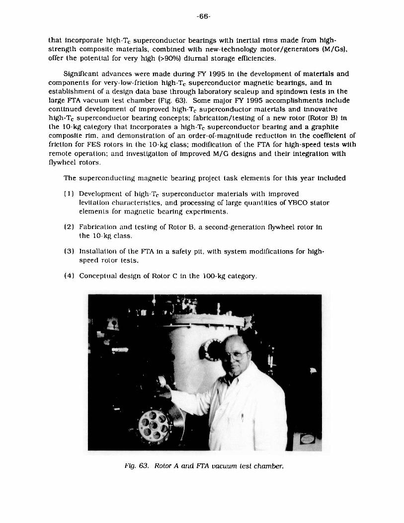
-66-
that incorporate high-Te superconductor bearings with inertial rims made from high-strength composite materials, combined with new-technology motor/generators (M/Gs),offer the potential for very high (>90%) diurnal storage efficiencies.
Significant advances were made during FY 1995 in the development of materials andcomponents for very-low-friction high-Ta superconductor magnetic bearings, and inestablishment of a design data base through laboratory scaleup and spindown tests in thelarge FTA vacuum test chamber (Fig. 63). Some major FY 1995 accomplishments includecontinued development of improved high-Ta superconductor materials and innovativehigh-Ta superconductor bearing concepts; fabrication/testing of a new rotor (Rotor B) inthe 10-kg category that incorporates a high-Ta superconductor bearing and a graphitecomposite rim, and demonstration of an order-of-magnitude reduction in the coefficient offriction for FES rotors in the 10-kg class; modification of the FTA for high-speed tests withremote operation; and investigation of improved M/G designs and their integration withflywheel rotors.
The superconducting magnetic bearing project task elements for this year included
(1) Development of high-Tc superconductor materials with improvedlevitation characteristics, and processing of large quantities of YBCO statorelements for magnetic bearing experiments.
(2) Fabrication and testing of Rotor B, a second-generation flywheel rotor inthe 10-kg class.
(3) Installation of the FTA in a safety pit, with system modifications for high-speed rotor tests.
(4) Conceptual design of Rotor C in the 100-kg category.
Fig. 63. Rotor A and FTA vacuum test chamber.

-67-
(5) Upgrade of the FTA M/C system to operate at up to 30,000 r/min, andcontinuing development of advanced M/G units based on Halbach arrayconcepts.
(6) Modification of an existing thick-walled spin chamber for use in spin-to-failure tests of small flywheel rotors levitated by high-Ta superconductormagnetic bearings.
(7) Continuation of high-Te superconductor magnetic bearing bell-jarexperiments to investigate new design concepts on a small scale.
As reported earlier in this report, the levitation characteristics of bulk Y- 123 super-conductor elements continued to improve through the use of seeding for improvedstructure, enhanced melt-processing techniques, and other innovations. Many Y- 123 tileelements were melt processed at ANL for the high-Ta superconductor magnetic-bearingdevelopment efforts. The best Y-123 levitators were selected to construct the second-generation high-Ta superconductor magnetic-bearing stator array. In December 1994, thenew array was installed in the FTA liquid N2 cryochamber, replacing the original high-Tasuperconductor stator array. Outside dimensions that exceeded 20 cm were required forboth high-Ta superconductor stator arrays for effective levitation of Rotors A and B, withtheir associated 20-cm outer-diam ring magnets.
The technology for fabricating bulk high-Ta superconductor materials has progressedto the stage where it is now being transferred to commercial manufacturers (Todt et al.,1994; Todt et al., 1995a-c). Bulk Y- 123 tile elements are currently being fabricatedby Superconductive Components, Inc. (Columbus, OH), and will be used in the third-generation stator assembly that is to be installed in the FTA. The levitation characteristicsof each puck or tile are determined at ANL by force measurements with a standard ref-erence magnet and well-defined procedures.
The collaborative efforts with UGIMAG (Valparaiso, IN) continued in the developmentof high-strength permanent-magnet (PM) rotors. The impact of azimuthal inhomoge-neities and other characteristics of rare-earth PMs on rotor performance has continued tobe of interest. Spindown tests and characterization of the 20-cm outer-diam, double-ring,PM for Rotor B were completed. The azimuthal magnetic field homogeneity of the Rotor Bmagnet was significantly better than the previous Rotor A magnet of the same size. Figure64 shows the coefficient of friction measured in low-speed FTA spin tests for the Rotor Bpermanent magnet alone, without composite banding, as a function of rim velocity forthree levitation gap heights between the bottom of the magnet and the top of the high-Tasuperconductor array (Mulcahy et al., 1995).
Design of a 39-cm outer-diam graphite fiber/epoxy composite rim for Rotor B wascompleted as a collaborative effort that involved ANL, CRC, and Pennsylvania State Univer-sity (PSU). The composite rim was then fabricated by PSU. Rotor B is designed for higherrotational speeds than was the case for Rotor A. Following assembly of the rim, hub, andPM rings, spin tests of Rotor B were conducted in the FTA with the second-generationhigh-Ta superconductor stator array (Mulcahy et al., 1995). Coefficients of friction of -1 x
10-5 were achieved with Potor B during low-speed tests. Higher speed tests are scheduledfor early FY 1996.
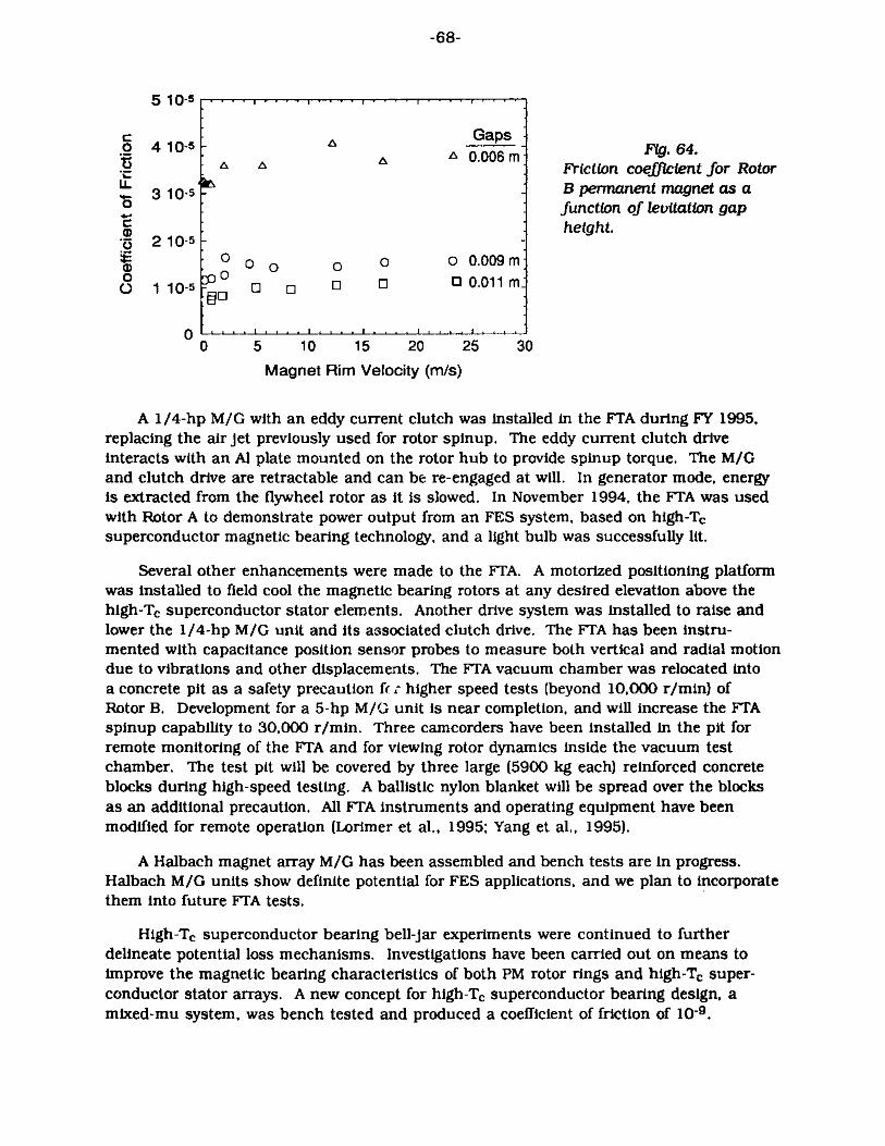
-68-
5 10-5 --- ---- .
o 4Gaps0 410-5 .o 6m FIg.64.
Friction coefficient for Rotor
3 10-5 B permanent magnet as afunction of levitation gap
21-5height.-v 2 10-5 --
0 0 0 0 0 0 O.009m
0 1010-5O0 Q o Q O 0.011 m
00 5 10 15 20 25 30
Magnet Rim Velocity (m/s)
A 1/4-hp M/G with an eddy current clutch was installed in the FTA during FY 1995,replacing the air jet previously used for rotor spinup. The eddy current clutch driveinteracts with an Al plate mounted on the rotor hub to provide spinup torque. The M/Gand clutch drive are retractable and can be re-engaged at will. In generator mode, energyis extracted from the flywheel rotor as it is slowed. In November 1994, the FTA was usedwith Rotor A to demonstrate power output from an FES system, based on high-Tcsuperconductor magnetic bearing technology, and a light bulb was successfully lit.
Several other enhancements were made to the FTA. A motorized positioning platformwas installed to field cool the magnetic bearing rotors at any desired elevation above thehigh-Tc superconductor stator elements. Another drive system was installed to raise andlower the 1/4-hp M/G unit and its associated clutch drive. The FTA has been instru-mented with capacitance position sensor probes to measure both vertical and radial motiondue to vibrations and other displacements. The FTA vacuum chamber was relocated intoa concrete pit as a safety precaution ft: higher speed tests (beyond 10,000 r/min) ofRotor B. Development for a 5-hp M/G unit is near completion, and will increase the FTAspinup capability to 30,000 r/min. Three camcorders have been installed in the pit forremote monitoring of the FTA and for viewing rotor dynamics inside the vacuum testchamber. The test pit will be covered by three large (5900 kg each) reinforced concreteblocks during high-speed testing. A ballistic nylon blanket will be spread over the blocksas an additional precaution. All FTA instruments and operating equipment have beenmodified for remote operation (Lorimer et al., 1995; Yang et al., 1995).
A Halbach magnet array M/G has been assembled and bench tests are in progress.Halbach M/G units show definite potential for FES applications, and we plan to incorporatethem into future FTA tests.
High-Tc superconductor bearing bell-Jar experiments were continued to furtherdelineate potential loss mechanisms. Investigations have been carried out on means toimprove the magnetic bearing characteristics of both PM rotor rings and high-Ta super-conductor stator arrays. A new concept for high-Ta superconductor bearing design, amixed-mu system, was bench tested and produced a coefficient of friction of 10-9.

-69-
References
R Abboud, J. Hull, K. Uherka, and T. Mulcahy, in Proc. Am. Power Conf., Vol. 56-II (1994)p. 1356.
T. R. Askew, J. G. Nestell, R. B. Flippen, D. M. Groski, and N. McN. Alford, IEEE Trans.Apple. Supercond. 3, 1398 (1993).
U. Balachandran, R. B. Poeppel, J. E. Emerson, and S. A. Johnson, U.S. Patent 5,086,034(Feb. 4, 1992).
U. Balachandran, et al., Practical Superconductor Development for Electrical PowerApplications: Annual Report for FY 1994, Argonne National Laboratory Report ANL-94/39(1994a).
U. Balachandran, A. N. Iyer, C. A. Youngdahl, L. R Motowidlo, and P. Haldar, Adv. Cryo. Eng.40 A, 289 (1994b).
U. Balachandran, U.S. Patent 5,409,887 (April 25, 1995).
U. Balachandran et al., in Advances in Superconductivity VII, Proc. 7th Intl. Symp. onSupercond. (ISS-94), Vol. 2 (Springer-Verlag, Tokyo, 1995a) p. 1243.
U. Balachandran, C. A. Youngdahl, M. T. Lanagan, S. E. Dorris, J. J. Picciolo, J. Cluff,T. Brent, M. Marinelli, B. Fisher, P. Winandy, J. Wenzlaff, T. Askew, R. C. Niemann, andR. B. Poeppel, Appl. Supercond., in press (1995b).
Y. S. Cha, M. T. Lanagan, K. E. Gray, V. Z. Jankus, and Y. Fang, Appl. Supercond. 2, 47(1994a).
Y. S. Cha, R. C. Niemann, and J. R. Hull, Cryogenics 34, 99 (1994b).
Y. S. Cha, W. J. Minkowycz, and S. Y. Seol, Int. Comm. Heat Mass Trans. 22, 461 (1995a).
Y. S. Cha, R. C. Niemann, and J. R. Hull, in Thermal Engineering 1995, Vol. 1, eds. L. S.Fletcher and T. Aihara (ASME, New York, 1995b) p. 115.
N. Chen, A. C. Biondo, S. E. Dorris, K. C. Goretta, M. T. Lanagan, C. A. Youngdahl, and R. B.Poeppel, Supercond. Sci. Technol. 6, 674 (1993).
J. A. DeLuca, P. L. Karas, J. E. Tkaczyk, C. L. Briant, M. F. Garbauskas, and P. J. Bednarczyk,Mater. Res. Soc. Symp. Proc. 275, 669 (1992).
L. P. De Rochemont, V. A. Maroni, M. Kugerman, R. J. Andrews, and W. C. Kelliher, Appl.Supercond. 2, 281 (1994).
S. E. Dorris, B. C. Prorok, M. T. Lanagan, S. Sinha, and R. B. Poeppel, Physica C 212, 66(1993).
S. E. Dorris, B. C. Prorok, M. T. Lanagan, N. M. Browning, M. R Hagen, J. A. Parrell, Y. Feng,A. Umezawa, and D. C. Larbalestier, Physica C 223, 163 (1994a).
S. E. Dorris, B. C. Prorok, M. T. Lanagan, V. A. Maroni, and R. B. Poeppel, U.S. Patent5,354,535 (October 11, 1994b).
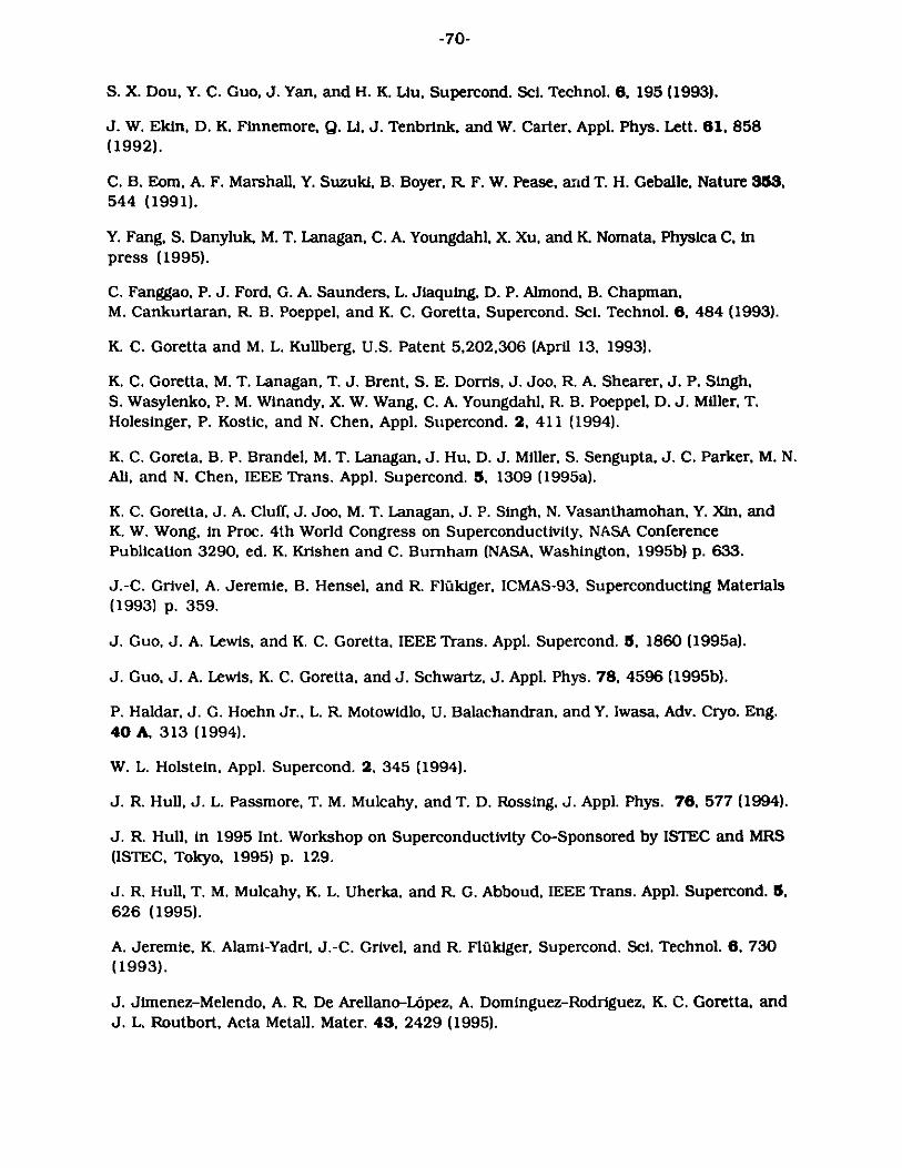
-70-
S. X. Dou, Y. C. Guo, J. Yan, and H. K. Liu, Supercond. Sci. Technol. 6, 195 (1993).
J. W. Ekin, D. K. Finnemore, Q. Li, J. Tenbrink, and W. Carter, Appl. Phys. Lett. 61, 858(1992).
C. B. Eom, A. F. Marshall, Y. Suzuki, B. Boyer, R F. W. Pease, and T. H. Geballe, Nature 353,544 (1991).
Y. Fang, S. Danyluk, M. T. Lanagan, C. A. Youngdahl, X. Xu, and K. Nomata, Physica C, inpress (1995).
C. Fanggao, P. J. Ford, G. A. Saunders, L. Jiaquing, D. P. Almond, B. Chapman,M. Cankurtaran, R. B. Poeppel, and K. C. Goretta, Supercond. Sci. Technol. 6, 484 (1993).
K. C. Goretta and M. L. Kullberg, U.S. Patent 5,202,306 (April 13, 1993).
K. C. Goretta, M. T. Lanagan, T. J. Brent, S. E. Dorris, J. Joo, R. A. Shearer, J. P. Singh,S. Wasylenko, P. M. Winandy, X. W. Wang, C. A. Youngdahl, R. B. Poeppel, D. J. Miller, T.Holesinger, P. Kostic, and N. Chen, Appl. Supercond. 2, 411 (1994).
K. C. Goreta, B. P. Brandel, M. T. Lanagan, J. Hu, D. J. Miller, S. Sengupta, J. C. Parker, M. N.All, and N. Chen, IEEE Trans. Apple. Supercond. 5, 1309 (1995a).
K. C. Goretta, J. A. Cluff, J. Joo, M. T. Lanagan, J. P. Singh, N. Vasanthamohan, Y. Xin, andK. W. Wong, in Proc. 4th World Congress on Superconductivity, NASA ConferencePublication 3290, ed. K. Krishen and C. Burnham (NASA, Washington, 1995b) p. 633.
J.-C. Grivel, A. Jeremie, B. Hensel, and R. Flikiger, ICMAS-93, Superconducting Materials(1993) p. 359.
J. Guo, J. A. Lewis, and K. C. Goretta, IEEE Trans. Apple. Supercond. 5, 1860 (1995a).
J. Guo, J. A. Lewis, K. C. Goretta, and J. Schwartz, J. Apple. Phys. 78, 4596 (1995b).
P. Haldar, J. G. Hoehn Jr., L. R. Motowidlo, U. Balachandran, and Y. Iwasa, Adv. Cryo. Eng.40 A, 313 (1994).
W. L. Holstein, Appl. Supercond. 2, 345 (1994).
J. R. Hull, J. L. Passmore, T. M. Mulcahy, and T. D. Rossing, J. Apple. Phys. 76, 577 (1994).
J. R. Hull, in 1995 Int. Workshop on Superconductivity Co-Sponsored by ISTEC and MRS(ISTEC, Tokyo, 1995) p. 129.
J. R. Hull, T. M. Mulcahy, K. L. Uherka, and R. G. Abboud, IEEE Trans. Apple. Supercond. 5,626 (1995).
A. Jeremie, K. Alami-Yadri, J.-C. Grivel, and R. Flukiger, Supercond. Sci. Technol. 6, 730(1993).
J. Jimenez-Melendo, A. R. De Arellano-L6pez, A. Dominguez-Rodriguez, K. C. Goretta, andJ. L. Routbort, Acta Metall. Mater. 43, 2429 (1995).
-71-
J. Joo, J. P. Singh, T. Warzynski, A. Grow, and R B. Poeppel, Appl. Supercond. 2, 401(1994).
P. Krishnaraj, M. Lelovic, N. G. Eror, and U. Balachandran, Physica C 215, 305 (1993).
M. T. Lanagan, D. S. Kupperman, G. A. Yaconi, S. H. Kilgore, and A. Saigal, IEEE Trans. Appl.Supercond. 5, 1475 (1995).
D. C. Larbalestier, X. Y. Cai, Y. Feng, H. Edelman, A. Umezawa, G. N. Riley, and W. L. Carter,Physica C 221, 299 (1994).
M. Lelovic, P. Krishnaraj, N. G. Eror, and U. Balachandran, Physica C 242, 246 (1995a).
M. Lelovic, P. Krshnaraj, N. G. Eror, and U. Balachandran, Supercond. Sci. Technol. 8, 336(1995b).
Y. F. Li, Z. Z. Sheng, S. Sengupta, K. C. Goretta, and P. E. D. Morgan, Physica C 232, 184(1994).
Y. F. Li, Z. Z. Sheng, Z. F. Ren, J. H. Wang, and K. C. Goretta, Supercond. Sci. Technol. 8,174 (1995).
W. L. Lorimer, D. K. Lieu, J. R. Hull, T. M. Mulcahy, and T. D. Rossing, IEEE Trans. Magn.30, 3004 (1994).
J. S. Luo, S. E. Dorris, M. T. Lanagan, and V. A. Maroni, Proc. Microscop. Soc. Am. 52, 798(1994a).
J. S. Luo, N. Merchant, E. J. Escorcia-Aparicio, V. A. Maroni, B. S. Tani, W. L. Carter, andG. N. Riley Jr., J. Mater. Res. 9, 3059 (1994b).
P. Majewski, B. Hettich, K. Schulze, and G. Petzow, Adv. Mater. 3, 488 (1991).
P. Majewski, S. Kaesche, H.-L. Su, and F. Aldinger, Physica C 221, 295 (1994).
V. A. Maroni, U.S. Patent 5,010,053 (April 23, 1991).
V. A. Maroni, U.S. Patent 5,079,233 (January 7, 1992).
L. J. Martin, K. C. Goretta, J. Joo, J. P. Singh, S. R. Olson, S. Wasylenko, R B. Poeppel, andN. Chen, Mater. Lett. 17, 232 (1993).
N. Merchant, J. S. Luo, V. A. Maroni, G. N. Riley Jr., and W. L. Carter, Appl. Phys. Lett. 65,1039 (1994a).
N. Merchant, J. S. Luo, V. A. Maroni, S. N. Sinha, G. N. Riley Jr., and W. L. Carter, Appl.Supercond. 2, 217 (1994b).
T. A. Miller, J. E. Ostenson, Q. Li, L. A. Schwartzkopf, D. K. Finnemore, J. Righi, R. A.Gleixner, and D. Zeigler, Appl. Phys. Lett. 58, 2159 (1991).
P. E. D. Morgan, M. Okada, T. Matsumoto, and A. Soeta, in Adv. Supercond. II; Proc. 2ndInt. Symp. on Superconductivity (ISS'89) eds. T. Ishiguro and K. Kajimura (Springer-Verlag, Berlin, 1990) p. 435.

-72-
T. M. Mulcahy, J. R Hull, K. L. Uherka, R G. Abboud, J. H. Wise, C. W. Gabrys, and C. E.Bakis, IEEE Trans. Magn., in press (1995).
R C. Niemann, Y. S. Cha, J. R Hull, W. E. Buckles, and M. A. Daugherty, Adv. Cryo. Eng. 39,1153 (1994a).
R C. Niemann, J. D. Gonczy, and T. H. Nicol, Adv. Cryo. Eng. 39, 1665 (1994b).
R C. Niemann, W. E. Buckles, Y. S. Cha, K. D. Dixon, J. R Hull, C. M. Rey, and B. R Weber,in Proc. 30th Intersociety Energy Conv. Eng. Conf., Vol. 3 (ASME, New York, 1995a) p. 293.
R C. Niemann, Y. S. Cha, J. R Hull, W. E. Buckles, B. R. Weber, and S. T. Yang, IEEE Trans.Appl. Supercond. 5, 793 (1995b).
R C. Niemann, Y. S. Cha, J. R. Hull, C. M. Rey, and K.D. Dixon, IEEE Trans. Appl.Supercond. 5, 789 (1995c).
R C. Niemann, J. D. Gonczy, and T. H. Nicol, in Thermal Engineering 1995, Vol. 1, ed. L. S.Fletcher and T. Aihara (ASME, New York, 1995d) p. 43.
R C. Niemann, J. D. Gonczy, and T. H. Nicol, U.S. Patent 5,356,870 (Feb. 7, 1995e).
S. Nomura, H. Fuke, H. Yoshino, and K. Ando, Supercond. Scd. Technol. 6, 858 (1993).
A. Otto, L. J. Masur, J. Gannon, E. Podtburg, D. Daly, G. J. Yurek, and A. P. Malozemoff, IEEETrans. Appl. Supercond. 3, 915 (1993).
M. Paranthaman and A. M. Hermann, in Organic Conductors: Fundamentals andApplications, ed. J. P. Farges (Marcel Dekker, New York, 1994) p. 735.
A. E. Pashitski, A. Polyanskii, A. Gurevich, J. A. Parrell, and D. C. Larbalestier, Physica C246, 133 (1995).
R.B. Poeppel et al., Practical Superconductor Development for Electrical PowerApplications- Annual Report for FY 1993, Argonne National Laboratory Report ANL-93/33(1993).
R B. Poeppel, K. C. Goretta, M. T. Lanagan, S. Danyluk, M. McNallan, and R Troendly, U.S.Patent application 08/317,353 (1994).
J. Polonka, M. Xu, A. Goldman, and D. K. Finnemore, J. Appl. Phys., 4, 7397 (1993).
Z. F. Ren and J. H. Wang, Physica C 216, 199 (1993).
Z. F. Ren, J. H. Wang, D. J. Miller, and K. C. Goretta, Physica C 229, 137 (1994).
Z. F. Ren, C. A. Wang, J. H. Wang, D. J. Miller, and K. C. Goretta, Physica C 247, 163 (1995).
T. D. Rossing and J. R. Hull, Quantum 5(4), 22 (1995).
R R Schartman, R. Sakidja, and E. E. Hellstrom, J. Am. Ceram. Soc. 76, 724 (1993).
J. P. Singh, J. Joo, D. Singh, T. Warzynski, and R. B. Poeppel, J. Mater. Res. 8, 1226 (1993).

-73-
J. P. Singh, D. Singh, D. S. Kupperman, and S. Maumdar, in High Performance Composites:Commonality of Phenomena, eds. K. K. Chawla, P. K. Liaw, and S. G. Fishman (FMS,Warrendale, 1994) p. 143.
J. P. Singh, R B. Poeppel, K. C. Goretta, and N. Chen, U.S. Patent 5,401,712 (March 28,1995).
M. Suenaga, Y. Fukumoto, and P. Haldar, unpublished information (1995).
M. Tetenbaum, M. C. Hash, B. S. Tani, J. S. Luo, and V. A. Maroni, Physica C 235-240, 321(1994).
M. Tetenbaum, M. C. Hash, B. S. Tani, J. S. Luo, and V. A. Maroni, Physica C 249, 396(1995).
V. R Todt, S. Sengupta, D. Shi, P. R. Sahm, P. J. McGinn, R. Poeppel, and J. R Hull,J. Electron. Mater. 23, 1127 (1994).
V. R Todt, D. J. Miller, and S. Sengupta, in 1995 Int. Workshop on SuperconductivityCo-Sponsored by ISTEC and MRS (ISTEC, Tokyo, 1995a) p. 355.
V. R. Todt, S. Sengupta and D. J. Miller, Appl. Supercond. 3, 175 (1995b).
V. R. Todt, S. Sengupta, D. J. Miller, Y. Chen, U. Balachandran, K. C. Goretta, and J. Guo,IEEE Trans. Apple. Supercond. 5, 1623 (1995c).
V. R Todt, S. Sengupta, and D. Shi, U.S. Patent Applications 08/372,042 and 08/372,067;V. R. Todt, S. Sengupta, D. J. Miller, and D. Shi, U.S. Patent Application 08/372,142(1995d).
C. Uher, J. Supercond. 3, 337 (1990).
Q. Wang, G. A. Saunders, M. Cankurtaran, D. P. Almond, and K. C. Goretta, Phys. Rev. B 52,3711 (1995).
U. Welp, D. 0. Gunter, G. W. Crabtree, J. S. Luo, V. A. Maroni, P. Haldar, R S. Sokolowski,V. K. Vlasko-Vlasov, and I. Nikitenko, Appl. Phys. Lett. 66, 1270 (1994).
U. Welp, D. 0. Gunter, G. W. Crabtree, W. Zhong, U. Balachandran, W. L. Carter, V. K. Vlasko-Vlasov, and I. Nikitenko, Nature 376, 44 (1995).
W. Wu, M. T. Lanagan, B. Wang, R. B. Poeppel, and S. Danyluk, Appl. Supercond. 2, 387(1994).
W. Wu, C.-Y. Chu, K. C. Goretta, and J. L. Routbort, U.S. Patent 5,411,938 (May 2, 1995).
M. Xu, D. K. Finnemore, U. Balachandran, and P. Haldar, Appl. Phys. Lett. 66, 3359 (1995a).
M. Xu, D. K. Finnemore, U. Balachandran, and P. Haldar, J. Apple. Phys. 78, 360 (1995b).
Z. J. Yang, J. R. Hull, T. M. Mulcahy, and T. D. Rossing, J. Appl. Phys. 78, 2097 (1995).

-74-
J. Yau and N. Savvides, Appl. Phys. Lett. 65, 1454 (1994).
G. 0. Zimmerman, Y. Z. Negm, M. Z. Tahar, R E. Powers, and R McConeghy, Physica C209, 291 (1993).

-75-
Distribution for ANL-95/42
T. AskewU. Balachandran (25)I. D. BloomY. S. ChaG. CrabtreeD. R DiercksS. E. DorrisH. DruckerB. DunlapJ. T. DusekW. A. EllingsonJ. E. EmersonB. L. FisherF. Y. FradinR GieseK. C. Goretta
K E. GrayD. GruenM. HanleyJ. R. HullJ. JorgensenR T. KampwirthM. KirkD. S. KuppermanS. LakeM. T. LanaganC. A. MalefytM. MarinelliV. A. MaroniR. L. McDanielD. J. MillerT. Mulcahy
R C. NiemannJ. J. PiccioloR B. PoeppelA. C. RaptisJ. L. RoutbortW. J. ShackW. W. SchertzJ. P. SinghC. E. TillK. L. UherkaA. WaghA. WantrobaR W. WeeksA. M. WolskyC. A. YoungdahlTIS Files
External:
DOE-OSTI, for distribution per UC-1394 (154)ANL Libraries
ANL-EANL-W
Chicago Field Office. DOE:ManagerF. Herbaty
U.S. Department of Energy. Washington:
Office of Advanced Utility Concepts, Conservation and Renewable Energy:J. DaleyR Eaton IIIC. KangC. Platt
Basic Energy Sciences-Materials Science, Energy Research:I. L. Thomas
Energy Technology Division Review Committee:H. K. Birnbaum, University of Illinois, UrbanaR C. Buchanan, University of Cincinnati, Cincinnati, OHS.-N. Liu, Fremont, CAH. S. Rosenbaum, Fremont, CA
I
-76-
R K. Shah, University of Kentucky, LexingtonS. Smialowska, Ohio State University, ColumbusR E. Smith, Altran Corp., Huntersville, NC
Other - Industry - UniversityR G. Abboud, Commonwealth Edison Co., Zion, ILJ. Badin, Energetics, Inc., Columbia, MDA. L. Bement, Jr., Midwest Superconductivity Consortium, Purdue UniversityT. Bickel, Sandia National LaboratoriesK. Blohowiak, Boeing Corporation, Seattle, WAR W. Boom, University of Wisconsin - MadisonJ. Bray, General Electric Company, Schenectady, NYW. Buckles, Superconductivity, Inc., Madison, WID. Burlone, BASF Corp., Enka, NCL. Capuano, Conductus, Sunnyvale, CAR Cass, HiTc Superconco, Inc., Lambertville, NJJ. Clem, Ames LaboratoryB. Currie, Pacific Northwest LaboratoryS. Danyluk, Georgia Institute of TechnologyM. DeGuire, Case Western Reserve UniversityL. P. de Rochemont, Radiation Monitoring Devices, Inc., Watertown, MAD. Divecha, Naval Surface Warfare Center, Silver Spring, MDB. Dorothy, DuPont, Wilmington, DED. Driscoll, Reliance Electric, ClevelandM. Eddy, Superconductor Technologies, Inc., Santa Barbara, CAN. Eror, University of PittsburghD. K. Finnemore, Ames LaboratoryM. Fluss, Lawrence Livermore National LaboratoryS. Foner, Francis Bitter National Magnet Lab., Massachusetts Institute of TechnologyJ. R Gaines, Jr., Superconductive Components, Inc., Columbus, OHC. Gallo, Superconix, St. Paul, MNT. Grudkowski, United Technologies Research Center, East Hartford, CTD. Gubser, Naval Research LaboratoryP. Haldar, Intermagnetics General Corp., Latham, NYS. D. Harkness, Westinghouse, PittsburghR A. Hawsey, Oak Ridge National LaboratoryJ. Hodge, Illinois Superconductor Corp., Mt. Prospect, ILD. L. Johnson, Northwestern UniversityJ. B. Ketterson, Northwestern UniversityJ. L. Kirtley, Jr., Massachusetts Institute of TechnologyM. Klein, University of Illinois, UrbanaS. F. Kral, Babcock & Wilcox, Lynchburg, VAD. K. Kroeger, Oak Ridge National LaboratoryH. Kroger, Microelectronics and Computer Technology Corporation, Austin, TXD. C. Larbalestier, University of Wisconsin - MadisonA. Lauder, DuPont, Wilmington, DEE. Leung, Lockheed Martin, San Diego, CAM. Levy, University of Wisconsin - MilwaukeeJ. Lewis, University of Illinois, UrbanaD. H. Liebenberg, Office of Naval Research, Arlington, VA

-77-
P. Lindhorst, MagneTek, St. LouisR. Loehman, Sandia National LaboratoriesJ. Loncoski, Virginia Power, Glen Allen, VAH. Madler, J. C. Petlau, Inc., Wheeling, ILD. Madura, General Dynamics, San Diego, CAA. Malozemoff, American Superconductor Corp., Westborough, MAK. Marken, Oxford Instruments, Inc., Carteret, NJC. Martin, SSC, Inc., Woodinville, WAA. Marwick, IBM, Yorktown Heights, NYT. Mason, Northwestern UniversityR Mathisen, Foster-Miller, Inc., Waltham, MAB. McConnell, National Renewable Energy LaboratoryP. J. McGinn, University of Notre DameD. Moon, Westinghouse, PittsburghM. W. Morgan, Ability Engineering Technology, Inc., South Holland, ILL. Motowidlo, IGC Advanced Superconductors, Inc., Waterbury, CTW. Nellis, Lawrence Livermore National LaboratoryC. A. Parker, AlliedSignal, Inc., Des Plaines, ILD. Peterson, Los Alamos National LaboratoryN. Phillips, Lawrence Berkeley National LaboratoryT. Pillai, Department of Physics, University of Wisconsin, LaCrosseR Raman, Ceracon, Sacramento, CAR. F. Ranellone, Newport News Shipbuilding, Newport News, VAR A. Roehl, Commonwealth Edison Co., ChicagoC. H. Rosner, Intermagnetics General Corp., Latham, NYJ. Schwartz, Florida State UniversityD. K. Sharma, Electric Power Research Institute, Palo Alto, CAS. Sinha, University of Illinois, ChicagoG. Smith, SSC, Inc., Woodinville, WA0. Smith, Illinois Superconductor Corp., Mt. Prospect, ILD. M. Smyth, Lehigh UniversityM. Suenaga, Brookhaven National LaboratoryP. T. Tsivitse, Reliance Electric, ClevelandR Weber, Containerless Research, Inc., Evanston, ILB. Weinberger, United Technologies Research Center, East Hartford, CTD. O. Welch, Brookhaven National LaboratoryR. E. Williams, Ocean and Atmospheric Science, Inc., Dobbs Ferry, NYJ. Worth, Oxford Instruments, Inc., Carteret, NJJ. Wu, Westinghouse Electric Corporation, Science and Technology Center, PittsburghG. J. Yurek, American Superconductor Corporation, Westborough, MAC. Zahopoulos, Northeastern UniversityG. O. Zimmerman, ZerRes Corp., Boston