Embed Size (px)
Citation preview

PracticalComputerAnalysis of
Switch ModePower Supplies
Copyright 2005 by Taylor & Francis Group, LLC
www.IranSwitching.ir

A CRC title, part of the Taylor & Francis imprint, a member of theTaylor & Francis Group, the academic division of T&F Informa plc.
PracticalComputerAnalysis of
Switch ModePower SuppliesJOHNNY C. BENNETT
Boca Raton London New York Singapore
Copyright 2005 by Taylor & Francis Group, LLC
www.IranSwitching.ir

Published in 2005 byCRC PressTaylor & Francis Group 6000 Broken Sound Parkway NW, Suite 300Boca Raton, FL 33487-2742
© 2005 by Taylor & Francis Group, LLCCRC Press is an imprint of Taylor & Francis Group
No claim to original U.S. Government worksPrinted in the United States of America on acid-free paper10 9 8 7 6 5 4 3 2 1
International Standard Book Number-10: 0-8247-5387-9 (Hardcover) International Standard Book Number-13: 978-0-8247-5387-0 (Hardcover) Library of Congress Card Number 2005050581
This book contains information obtained from authentic and highly regarded sources. Reprinted material isquoted with permission, and sources are indicated. A wide variety of references are listed. Reasonable effortshave been made to publish reliable data and information, but the author and the publisher cannot assumeresponsibility for the validity of all materials or for the consequences of their use.
No part of this book may be reprinted, reproduced, transmitted, or utilized in any form by any electronic,mechanical, or other means, now known or hereafter invented, including photocopying, microfilming, andrecording, or in any information storage or retrieval system, without written permission from the publishers.
For permission to photocopy or use material electronically from this work, please access www.copyright.com(http://www.copyright.com/) or contact the Copyright Clearance Center, Inc. (CCC) 222 Rosewood Drive,Danvers, MA 01923, 978-750-8400. CCC is a not-for-profit organization that provides licenses and registrationfor a variety of users. For organizations that have been granted a photocopy license by the CCC, a separatesystem of payment has been arranged.
Trademark Notice: Product or corporate names may be trademarks or registered trademarks, and are used onlyfor identification and explanation without intent to infringe.
Library of Congress Cataloging-in-Publication Data
Bennett, Johnny C.Practical computer analysis of switch mode power supplies / Johnny C. Bennett.
p. cm.Includes bibliographical references and index. ISBN 0-8247-5387-91. Switching power supplies--Computer simulation. I. Title.
TK7881.15.B46 2005621.31'7--dc22 2005050581
Visit the Taylor & Francis Web site at http://www.taylorandfrancis.com
and the CRC Press Web site at http://www.crcpress.com
Taylor & Francis Group is the Academic Division of T&F Informa plc.
DK1137_Discl.fm Page 1 Tuesday, July 5, 2005 2:29 PM
Copyright 2005 by Taylor & Francis Group, LLC
www.IranSwitching.ir

Preface
For many years prior to the 1970s, engineers designed and built switch modepower supplies (SMPSs) using methods based largely on intuitive and exper-imentally derived techniques. In general, these power supplies were able toachieve their primary goal of high-efficiency power conversion; unfortu-nately, due to the lack of adequate theoretical analysis techniques, many ofthese power supplies only marginally met their desired performance require-ments. In many cases, they were considered to be unreliable. Although theyappeared to be very simple in concept, these switching regulators exhibitedphenomena that were not understood and certainly could not be analyzed.
Things began to improve, however, in the early 1970s, when Dr. R.D. Mid-dlebrook and his group of students at the California Institute of Technologydeveloped the powerful circuit-averaging techniques, thus opening the doorfor the application of conventional linear circuit analysis methods. With thesetools brought to bear, the many subtle complexities of the conceptually “simple”switching regulator were soon understood, allowing engineers to designSMPSs with improved performance and higher reliability. At this point, thepower electronics field began to expand rapidly as better components weredeveloped, power conversion technology advancements were made, andsophisticated computer-aided design and analysis methods were utilized.
Having been in the power electronics field for many years, I have had thegood fortune to be involved with the design and analysis of many differenttypes of power supplies. Here in this book, one of my goals is to provide thereader with a good understanding of the essential requirements for analyzingthe switching regulated power supply performance characteristics. Anothergoal is to further demonstrate the power of the circuit-averaging technique byusing computer circuit simulation programs to provide the desired performanceanalyses. At this point, I would like to reference the very important work ofDr. Vincent Bello, who, in his seminal paper,
9
pointed the way to using theSPICE-based computer circuit simulator to perform linear small signal analysisand nonlinear large signal transient performance analysis as well. The simula-tion techniques presented in this book are based almost entirely on Dr. Bello’sapproach. There have been several theoretical and practical contributors to theadvancement of the circuit-averaging techniques over the years and I hope thatthe information presented here can help to further these advancements.
• Chapter 1 is a refresher of the basics of SMPS fundamentals andcircuit-averaging modeling. This may also be a primer for the new-comer, but it is recommended that the beginner read the referencedworks to obtain a more complete understanding.
DK1137_C000.fm Page v Monday, June 20, 2005 2:18 PM
Copyright 2005 by Taylor & Francis Group, LLC
www.IranSwitching.ir

• Chapter 2 provides information on the general analysis requirementsof a power supply. This is deemed necessary because it is equallyimportant to know what questions to ask as it is to provide theanswers.
• Chapter 3 gives information on how to develop the general types ofSMPS models and demonstrates the analysis approach using aSPICE-based circuit simulator.
• Chapter 4 looks, in a practical way, at most of the basic first-ordertypes of analysis generally associated with SMPS performance.
• Chapter 5 provides more practical and detailed information ondeveloping an SMPS and SMPS component models.
• In Chapter 6, three power supplies are analyzed in practical detail.In these examples, emphasis is placed on using the circuit-averagingmacromodel of the integrated circuit PWM controller. This is felt tosimplify and expedite the analysis of a particular design that usesthese commercially available controllers. As circuits and systemsbecome larger and more complex, the macromodel approach willcontinue to increase in importance in almost all areas of electroniccircuit analysis. The PWM macromodeling effort presented here willhopefully lead to the future development of many more such mac-romodels for commercially available PWM controllers, as has beenthe case with macromodels for transistors, op amps, etc.
• Appendix A deals with the optimal design of SMPS input filters.This is included here simply because of the fundamental importanceof this subject to any power supply.
• Appendix B provides the first-order approach used in developingthe macromodel for two commercially available PWM controllers.As was stated earlier, this is only a first step and hopefully will leadto the advancement and further development of these macros.
Although they are very important aspects of any switch mode powersupply, the analyses of actual switching circuits per se are not specificallyaddressed in this book. For our purposes, these switching circuits are con-sidered to be in the realm of conventional electronic circuit transient analysisand not implicitly related to the performance of an SMPS. There may beexceptions to this, of course.
I would like to express my thanks and appreciation to all the wonderfulpeople with whom I have worked over the years who have shared theirinvaluable knowledge and experiences. I would also like to expressly thankCol. William T. McLyman of the Jet Propulsion Laboratory for his encour-agement and for being instrumental in producing this book.
Johnny C. Bennett
DK1137_C000.fm Page vi Monday, June 20, 2005 2:18 PM
Copyright 2005 by Taylor & Francis Group, LLC
www.IranSwitching.ir

Author
Johnny C. Bennett is a native of the state of Louisiana and is a graduate ofLouisiana Tech University. He received his BSEE in 1964 and has worked asan electronics engineer over the past 40 years specializing in analog andpower electronics circuit design. He has worked for many of the top tech-nological companies both as an employee and as a consultant. Johnny’shobbies are reading, music, genealogy, and traveling. He currently residesin the city of South Lake Tahoe, California, and is the father of two adult sons.
DK1137_C000.fm Page vii Monday, June 20, 2005 2:18 PM
Copyright 2005 by Taylor & Francis Group, LLC
www.IranSwitching.ir

Contents
1
Review of Switch Mode Power Supply Fundamentals
1.1 Basic Topologies1.1.1 Buck Converter — Continuous Mode1.1.2 Buck Converter — Discontinuous Mode1.1.3 Boost Converter — Continuous Mode1.1.4 Boost Converter — Discontinuous Mode1.1.5 Buck–Boost Converter — Continuous Mode1.1.6 Buck–Boost Converter — Discontinuous Mode
1.2 Basic Control Methods1.2.1 Frequency of Operation Factors (FOFs)1.2.2 Voltage Mode Control 1.2.3 Current Mode Control1.2.4 Feedback and Feedforward Control Additions
1.3 Conclusion
2
SMPS Analysis Requirements
2.1 DC Requirements2.1.1 Output Regulation 2.1.2 Cross Regulation with Multiple Outputs2.1.3 Efficiency2.1.4 Miscellaneous Range and Threshold Considerations
2.2 AC Requirements2.2.1 AC Control Loop Stability Margins2.2.2 Input Filter Stability Margins2.2.3 Source and Load Stability Margins2.2.4 Electromagnetic Compatibility
2.3 Transient Requirements2.3.1 Load Transients 2.3.2 Line Transients2.3.3 Power-Up and Power-Down Transients2.3.4 Energy Storage for Line Dropouts
2.4 Summary
3
Fundamental Switch Mode ConverterModel Development
3.1 Buck and Boost Converter Continuous ModeLarge Signal Models
DK1137_C000.fm Page ix Monday, June 20, 2005 2:18 PM
Copyright 2005 by Taylor & Francis Group, LLC
www.IranSwitching.ir

3.2 Buck and Boost Converter Discontinuous ModeLarge Signal Models
3.3 Buck and Boost Continuous and DiscontinuousMode Unified Models
3.4 Buck–Boost (Flyback) Converter ContinuousMode Large Signal Model
3.5 Buck–Boost (Flyback) Converter DiscontinuousMode Large Signal Model
3.6 Buck–Boost Continuous and DiscontinuousMode Unified Model
3.7 Cuk Converter Continuous ModeLarge Signal Model
3.8 Cuk Converter Discontinuous Mode Large Signal Model3.9 Cuk Converter Continuous and Discontinuous
Mode Unified Model3.10 Boost Converter Model Analysis Example 3.11 Summary
4
Analyzing the Fundamental SMPS Model
4.1 Buck Converter SMPS Analysis (Voltage Mode)4.1.1 Voltage Mode Converter Model Setup4.1.2 Open Loop Analysis (Continuous and
Discontinuous Modes)4.1.2.1 Forward Transfer Function 4.1.2.2 Output Impedance (Voltage Mode)4.1.2.3 Control to Output (Voltage Mode)
4.1.3 SMPS Closed Loop Analysis (Continuousand Discontinuous Modes)4.1.3.1 AC Loop Gain (Voltage Mode)4.1.3.2 SMPS Output Impedance (Voltage Mode)4.1.3.3 SMPS Line Regulation (Voltage Mode)4.1.3.4 SMPS Feedforward Analysis
4.1.4 SMPS Combined Feedback and FeedforwardAnalysis (Line Regulation)
4.2 Buck Converter SMPS Analysis (Current Mode)4.2.1 Current Mode Converter Model Setup4.2.2 Open Voltage Loop AC Analysis (Continuous and
Discontinuous Modes)4.2.2.1 Open Voltage Loop AC Output Impedance
(Current Mode) 4.2.2.2 Open Voltage Loop Forward Transfer
Function (Current Mode) 4.2.2.3 Control to Output Analysis (Current Mode)4.2.2.4 Inner Inductor Current Control Loop Gain
DK1137_C000.fm Page x Monday, June 20, 2005 2:18 PM
Copyright 2005 by Taylor & Francis Group, LLC
www.IranSwitching.ir

4.2.3 SMPS Closed Loop Analysis (Current Mode)4.2.3.1 SMPS Output Impedance (Current Mode)4.2.3.2 SMPS Line Regulation (Current Mode)
4.3 Summary
5
SMPS Component Models
5.1 Component Model Development5.1.1 Real-World Capacitor Macro.5.1.2 Real-World Inductor Macro5.1.3 SMPS Diode Macro5.1.4 Integrated Circuit Controllers
5.2 Parasitic Resistance Effects5.3 Peripheral Circuit Additions
5.3.1 Input Filter5.3.2 Inrush Current Limiter5.3.3 Undervoltage Lockout and Soft Start Circuits5.3.4 Power Factor Correction Circuits5.3.5 Multiple Outputs5.3.6 Postregulated Output Circuits5.3.7 Synchronous Rectifier Circuits5.3.8 Energy Storage Systems
5.4 Summary
6
Analyzing the Advanced SMPS Model
6.1 Pulse Width Modulator (PWM) Controller Macromodel6.2 Practical Flyback SMPS Analysis
6.2.1 Flyback SMPS Model Setup6.2.2 Flyback SMPS Large Signal Power ON/OFF Analysis6.2.3 Flyback SMPS Large Signal Load and Line
Transient Analysis6.2.4 Flyback SMPS Current-Limiting Performance6.2.5 Flyback SMPS AC Stability Analysis6.2.6 Flyback SMPS AC Line Rejection Analysis
6.3 Practical Buck SMPS Analysis with Parasitic Resistances6.3.1 Practical Buck Converter Model Development
with Parasitic Resistances6.4 Practical “Loop-Opening” Techniques for AC Analysis6.5 Buck SMPS Soft Start and “Hiccup” Current Limit Analysis6.6 Summary
Appendix A
Design Fundamentals of SMPS Input Filters
A.1 General RequirementsA.2 Fundamental Single-Stage LC Section Examples
DK1137_C000.fm Page xi Monday, June 20, 2005 2:18 PM
Copyright 2005 by Taylor & Francis Group, LLC
www.IranSwitching.ir

A.3 Parallel Damped Single-Stage Input FilterA.4 Series Damped Single Stage Input FilterA.5 Two-Stage Input Filter Design
Appendix B
Pulse Width Modulator ControllerMacromodeling
B.1 UC 1844 Circuit-Averaging Macromodel DevelopmentB.2 UC 1825A Circuit-Averaging Macromodel Development
References
DK1137_C000.fm Page xii Monday, June 20, 2005 2:18 PM
Copyright 2005 by Taylor & Francis Group, LLC
www.IranSwitching.ir

1
1
Review of Switch Mode Power Supply
Fundamentals
A switch mode power supply (SMPS) may in general be defined as any typeof electronic circuit that converts and/or regulates voltage or current byutilizing switching circuits and energy storage elements (capacitors andinductors). These circuits are ideally lossless with 100% energy transfer. Thisbeginning chapter will provide a review of the most basic power convertertopologies in their simplest form and an explanation of all their variousmodes of operation and control.
1.1 Basic Topologies
There are basically three fundamentally defined switch mode power supplyconverter topologies: the buck, the boost, and the combined form generallyreferred to as the buck–boost converter. Each of these converters has itsunique properties and, in general, is applied in a complementary manner toeach of the others. Also, each may have the capability of operating in oneof two fundamental modes: the continuous mode or the discontinuous mode.These will be discussed in detail in the following sections.
1.1.1 Buck Converter — Continuous Mode
As an immediate initiation to the fundamentals, consider an illustrationusing the simplest example of all: the elementary buck converter. (Presum-ably, the defining word “buck” is deduced from the fact that the input voltageis bucked, or attenuated, in amplitude and a lower amplitude voltage appearsat the output.) Figure 1.1a shows the circuit topology and Figure 1.1b showsthe defining current and voltage waveforms. The switch positions
d
and
d
′
represent the fraction of time that the periodically toggling switch remainsin each position. (The period
dT
P
is generally referred to as the converterON time and the period
d
′
T
P
is called the converter OFF time.) By assigninga period duration of unity, it can then be seen that
d
+
d
′
=
1. The switchingperiod,
dT
P
, occurs at a frequency that is much greater than the cut-off
DK_1137.book Page 1 Wednesday, June 15, 2005 11:49 AM
Copyright 2005 by Taylor & Francis Group, LLC
www.IranSwitching.ir

2
Practical Computer Analysis of Switch Mode Power Supplies
frequency of the LC low-pass filter; thus, it provides the average or DCcomponent of the switched or “chopped” input voltage,
v
IN
, to the load withan attenuated and desired very low AC ripple component. The large signalnonlinear transfer function of this converter is indicated in Equation 1.1.
(1.1)
FIGURE 1.1
Basic buck converter: a) topology; b) continuous mode waveforms.
+
vIN
Ideal SwitchThat
TogglesPeriodically
at TP
d
d’
L
C RLoad
iL iOUTiIN
a)
iIN
VINvI
VOUT = d x VIN
TP
d’TPdTP0
0
0
iL
iIN (AVG)
b)
iOUT
iRIPPLE
v1 vOUT
v dvOUT IN=
DK_1137.book Page 2 Wednesday, June 15, 2005 11:49 AM
Copyright 2005 by Taylor & Francis Group, LLC
www.IranSwitching.ir
Review of Switch Mode Power Supply Fundamentals
3
A small signal linear model developed by Middlebrook and Cuk
1,2
thathas achieved wide acceptance is shown in Figure 1.2. This canonical modelis applicable to all three basic topologies operating in the continuous mode;the different circuit component parameters are noted in the table in thisfigure. The different facets of each topology will be discussed in the followingcorresponding sections. This linearized model is used to allow all of thelinear circuit analysis techniques developed over the years to be appliedwhen analyzing a power supply at a particular DC operating point. Notethe dependent voltage and current generators. Some important observationsare immediately noted.
First, when a feedback control from the output is used to control , it isimmediately obvious that the two-pole LC filter presents a “sticky” AC stabilityconcern that must be dealt with. Next, with an ideal input voltage source — thatis, with zero source impedance — the dependent current generator is essentially
FIGURE 1.2
Basic SMPS continuous conduction mode canonical model.
N a f(s) Le
BuckD D
11 L
Boost
D1
1
− D1
1
−⎟⎠⎞
⎟⎠⎞
⎜⎝⎛
⎜⎝⎛
−R
Les1 ( )2D1
L
−Buck Boost
D1
D
− ( )D1D
D
−−
R
DLs1 e
( )2D1
L
−
OUTOUT vVv +=
dDd += (DC + incremental quantities)
CR
+
Le
+
1 : N
ININ vV +
( )dsaVf
dRV
a ⎜⎠
⎞⎜⎝
⎛
OUTOUT vV +
. .
ININ vVv +=
d
DK_1137.book Page 3 Wednesday, June 15, 2005 11:49 AM
Copyright 2005 by Taylor & Francis Group, LLC
www.IranSwitching.ir
4
Practical Computer Analysis of Switch Mode Power Supplies
shorted and has no effect on the output control; the dependent voltagegenerator provides output voltage control through the two-pole LC filter. Itis then recognized that when real-world power sources with finite sourceimpedances are used, the control, , to output,
v
, will be affected by thisdependent current generator.
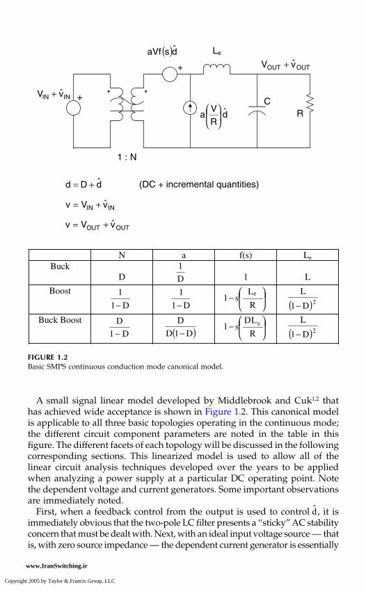
1.1.2 Buck Converter — Discontinuous Mode
Figure 1.3a shows a more realistic representation of the buck converter inwhich the ideal switch is replaced by the transistor switch and a catch diodecombination. When the load current,
i
OUT
, is reduced to a value that causesthe average inductor current to be less than one-half the inductor ripplecurrent,
∆
i
L
, the inductor current wants to flow negatively through theinductor. However, with the transistor switch off and the catch diodereversed biased, the negative inductor current has no path along which toflow. At this point, no current will flow in the inductor for the remainderof the converter OFF time. With this discontinuity in the inductor current,this mode of operation is generally referred to as the discontinuous mode.(Sometimes this zero inductor current condition is referred as “the inductorrunning dry.”)
Figure 1.3b shows the defining current and voltage waveforms with obvi-ous differences noted between those of the continuous mode in Figure 1.1b.The converter OFF time for this mode of operation is generally designatedin a different way. The portion of the OFF time during which inductor currentis still flowing is designated as
d
2
t
p
, and it is now recognized that
d
+
d
2
<
1.The convention for this was established in Cuk and Middlebrook
3
in thecourse of their pioneering work in the development of analytical powerconverter models. The transfer function for the discontinuous mode is notedin Equation 1.2 and is not as simple a relationship as that of the continuousmode. It is now a function of
d
, output load current,
i
OUT
, and the ratio of
L
/
t
p
.Middlebrook
3
defines a “conduction parameter,”
k
=
2
L
/
Rt
P
, that denotesthe boundary between continuous and discontinuous modes. For the buckconverter,
k
=
D
′
at this boundary. This relationship can be derived veryeasily from the waveforms shown in Figure 1.1b and Figure 1.3b.
(1.2)
where
(1.2a)
d
v vk
d
OUT IN=+ +
⎛
⎝
⎜⎜⎜⎜
⎞
⎠
⎟⎟⎟⎟
2
1 14
2
kL
RTP
= 2
DK_1137.book Page 4 Wednesday, June 15, 2005 11:49 AM
Copyright 2005 by Taylor & Francis Group, LLC
www.IranSwitching.ir

Review of Switch Mode Power Supply Fundamentals
5
and
(1.2.b)
FIGURE 1.3
Basic buck converter: a) topology; b) discontinuous mode waveforms.
iOUT
iD
iIN
v1
VOUT
TP
d2TPdTP0
0
0
iL
iIN (AVG)
b)
iOUT
Li∆
iD
0
iLiIN vOUT
a)
L
C RLOAD+ iD
D
Q
Q on forPeriod “d”
v1
vIN
VIN
RVI
OUT
OUT
≡
DK_1137.book Page 5 Wednesday, June 15, 2005 11:49 AM
Copyright 2005 by Taylor & Francis Group, LLC
www.IranSwitching.ir

6
Practical Computer Analysis of Switch Mode Power Supplies
1.1.3 Boost Converter — Continuous Mode
The simple boost converter is shown in Figure 1.4a; as its name implies, itsteps up or “boosts” the input voltage to a level higher than that of the inputvoltage. This topology is considered the “dual” or complement of the buck
FIGURE 1.4
Basic boost converter: a) topology; b) continuous mode waveforms.
a)
L
C RLOAD
iOUT
+
iIN = iLiD
D
QQ on forPeriod “d”
v1vOUT
vIN
iQ
iD
VOUT
v1
VOUT = VIN/d’
TP
d’TPdTP0
0
0
iL
iIN (AVG)
b)
iOUT
iRIPPLE
0
iQ
DK_1137.book Page 6 Wednesday, June 15, 2005 11:49 AM
Copyright 2005 by Taylor & Francis Group, LLC
www.IranSwitching.ir

Review of Switch Mode Power Supply Fundamentals
7
converter. See Cuk and Middlebrook
4
for more detail on the unique relation-ships between all of these fundamental converter topologies.
The defining voltage and current waveforms are shown in Figure 1.4b.One of the interesting dualities noted in comparing the continuous modeboost and buck converters is that the input current to the buck converter ispulsating or “chopped,” as noted in Figure 1.1b; however, because of theinductor on the input side, the input current to the boost converter is non-pulsating or relatively smooth, as noted in Figure 1.4b. Conversely, theoutput current of the boost converter,
i
D
, which is averaged by the outputfilter capacitor, is chopped, but the output current of the buck converter,
i
L
,is smooth as a result of the inductor on the output side. The transfer functionof this converter is indicated in Equation 1.3.
(1.3)
Note in Figure 1.2 that the boost converter small signal model is a littlemore complex than that of the buck converter in that the equivalent outputfilter inductor,
L
e
, is not simply
L
but is actually a function of the operatingpoint duty ratio,
D
. Also note that the dependent voltage source generatorhas a right-half plane (RHP) zero associated with it. This makes the ACstability problem even more difficult.
A brief word regarding this RHP zero might be made here. This zero resultsbecause, when the duty ratio changes with time, the output voltage actuallyshifts in the opposite direction during this change because of the lagginginductor current change. When this converter is modeled for a computersmall signal circuit simulation, this RHP zero can sometimes present a prob-lem. If so, the way to deal with it is to manipulate the circuit model by slidingthe dependent current generator to the right of the inductor; the RHP zerowill disappear from the model. This is essentially backing through the der-ivation of the canonical model. See Middlebrook and Cuk
1
for details.
1.1.4 Boost Converter — Discontinuous Mode
As one might expect, the discontinuous mode boost converter exhibits thesame dual relationships with the buck converter in the discontinuous modeas it did with the buck converter in the continuous mode. Figure 1.5a showsthe basic topology again, and Figure 1.5b shows the defining current andvoltage waveforms. Again, the discontinuous or zero inductor current con-dition is noted. The transfer function of this converter is indicated in Equa-tion 1.4 and has the same parametric dependencies as those of the buckdiscontinuous mode converter.
(1.4)
vvdOUTIN=′
v v
dk
OUT IN=+ +
⎛
⎝
⎜⎜⎜⎜
⎞
⎠
⎟⎟⎟⎟
1 14
2
2
DK_1137.book Page 7 Wednesday, June 15, 2005 11:49 AM
Copyright 2005 by Taylor & Francis Group, LLC
www.IranSwitching.ir

8
Practical Computer Analysis of Switch Mode Power Supplies
1.1.5 Buck–Boost Converter — Continuous Mode
The continuous mode buck–boost converter is in essence a cascaded versionof the buck and boost converter with a transfer function of:
(1.5)
FIGURE 1.5
Basic boost converter: a) topology; b) discontinuous mode waveforms.
a)
L
C RLOAD
iOUT
+
iIN = iLiD
D
QQ on forPeriod “d”
v1 vOUT
vIN
iQ
VINV1
VOUT
TP
d2TPdTP
0
0
iL iIN (AVG)
Li∆
0
iQ
iD
b)
0
iOUT (AVG)
v vddOUT IN=
′⎛⎝⎜
⎞⎠⎟
DK_1137.book Page 8 Wednesday, June 15, 2005 11:49 AM
Copyright 2005 by Taylor & Francis Group, LLC
www.IranSwitching.ir

Review of Switch Mode Power Supply Fundamentals
9
The conventional, simple noninverting version of this topology is shownin Figure 1.6a. A coupled inductor is required for this representation. Theaccompanying waveforms are shown in Figure 1.6b. Note that the inputcurrent,
i
Q
, is a pulsating current and the current into the output filtercapacitor,
i
D
, is also a pulsating current. These pulsating currents are unde-sirable because they require more capacitive filtering to keep the ripplevoltages to an acceptable level. This particular buck–boost topology, orconventional “flyback” converter as it is generally called, unfortunatelyincorporates the worst ripple current characteristics of its constituent buck
FIGURE 1.6
Basic buck–boost converter: a) topology; b) continuous mode waveforms.
iD iOUT
a)
C
RLOAD+
iIN = iL = iQ
Q
Q on forPeriod “d”
v1
vINDL
vOUT1 : N
iD
v1
TP
d’TPdTP0
0
0
b)
iQ
iIN(AVG)
iOUT
vIN + vOUT
vIN
DK_1137.book Page 9 Wednesday, June 15, 2005 11:49 AM
Copyright 2005 by Taylor & Francis Group, LLC
www.IranSwitching.ir

10
Practical Computer Analysis of Switch Mode Power Supplies
and boost topologies. Around 1976, Dr. Slobodan Cuk developed his name-sake converter, the Cuk converter,
4
which provides the same buck–boosttransfer function as shown in Equation 1.5, but has smooth input and outputcurrents instead of the pulsating or chopped currents in the flyback con-verter. Figure 1.8a shows the fundamental inverting topology of the Cukconverter and Figure 1.8b shows the accompanying waveforms.
1.1.6 Buck–Boost Converter — Discontinuous Mode
Figure 1.7a shows the basic conventional, noninverting flyback converterwith the accompanying discontinuous mode waveforms in Figure 1.7b. The
FIGURE 1.7
Basic buck–boost converter: a) topology; b) discontinuous mode waveforms.
iD iOUT
a)
C
RLOAD+
iIN = iL = iQ
Q
Q on forPeriod “d”
v1
vINDL
vOUT1 : N
vINv1
VOUT
TP
d2TPdTP0
iIN (AVG)
0
iQ
iD
b)
0
iOUT (AVG)
DK_1137.book Page 10 Wednesday, June 15, 2005 11:49 AM
Copyright 2005 by Taylor & Francis Group, LLC
www.IranSwitching.ir

Review of Switch Mode Power Supply Fundamentals
11
transfer function is:
(1.6)
FIGURE 1.8
Cuk converter: a) topology; b) continuous mode waveforms.
a)
L1
C2RLOAD
iL2
+
iIN = iL1
DQQ on forPeriod “d”
v1 - vOUT
vIN
iQ C1
L2+ -
vIN
v1
TP
d’TPdTP0
iIN (AVG)iRIPPLE
VC1
0
0
iL1
iOUT(AVG)
iL2
b)
- VC1
vOUT
0
v2
v2
v v dkOUT IN= 1
DK_1137.book Page 11 Wednesday, June 15, 2005 11:49 AM
Copyright 2005 by Taylor & Francis Group, LLC
www.IranSwitching.ir

12
Practical Computer Analysis of Switch Mode Power Supplies
A general comparison between the discontinuous mode transfer functionsof the three basic topologies of Equation 1.2, Equation 1.4, and Equation 1.6shows that the flyback converter has the simplest discontinuous mode trans-fer function and the buck converter has the most complex. This is true despite
FIGURE 1.9
Cuk converter: a) topology; b) discontinuous mode waveforms.
a)
L1
C2RLOAD
iL2
+
iIN = iL1
DQQ on forPeriod “d”
v1 - vOUT
vIN
iQ C1
L2+ -
v2
vINv1
-vOUT
TP
d2TPdTP0
0
v2
0
iL1
+ i
b)
0
iL2
- i
DK_1137.book Page 12 Wednesday, June 15, 2005 11:49 AM
Copyright 2005 by Taylor & Francis Group, LLC
www.IranSwitching.ir

Review of Switch Mode Power Supply Fundamentals
13
the fact that the buck converter is the simplest derived converter and theflyback converter is more complex. The Cuk converter has the same discon-tinuous mode transfer function as the flyback (see Cuk
6
for details). Whenevaluating the parameter
k
, however, the value of inductance used in thecalculation is the parallel combination of
L
1 and
L
2. Figure 1.9a again showsthe fundamental inverting topology of the Cuk converter and Figure 1.9bshows the accompanying waveforms. It is interesting to note from Cuk
6
thatthe inductor currents
i
L
1
and
i
L
2
are both continuous or both discontinuousand that, in the general case, these currents do not individually become zerofor the discontinuous part of the switching cycle; rather, the sum of
i
L
1
and
i
L
2
becomes zero.
1.2 Basic Control Methods
When controlling the output of an SMPS, the proportion of time duringwhich the power switch is ON to the time during which it is OFF must beset by some controlling mechanism. The most commonly used defining termis the duty ratio,
d
, which is the ratio of the switch ON time to the totalswitch period. Several methods are used in accomplishing this pulse widthmodulation (PWM); they may be categorized into one of four categorieschosen to be identified by a “frequency of operation factors” definition:
• Constant frequency• Constant ON time • Constant OFF time• Constant hysteresis
Also, these four PWM techniques may generally be applied to either oneof two additional categories of control techniques known as voltage or cur-rent mode control. Voltage mode control uses the duty ratio control mecha-nism to control the output voltage directly; current mode control uses theduty ratio controller to regulate the current in the energy storage inductor.An additional outer control loop may then be implemented to regulate theoutput voltage if desired.
1.2.1 Frequency of Operation Factors (FOFs)
Constant frequency
. As the name implies, the switch cycle period is heldconstant with changes in converter ON time complementary to changes inconverter OFF time. This is the most commonly used control because thecontrol circuit may use a fixed frequency clock providing a very straightfor-ward and easy way to implement a control scheme. Also, frequency control
DK_1137.book Page 13 Wednesday, June 15, 2005 11:49 AM
Copyright 2005 by Taylor & Francis Group, LLC
www.IranSwitching.ir

14
Practical Computer Analysis of Switch Mode Power Supplies
may be desirable in efforts to control electromagnetic interference (EMI)phenomena emanating from the power converter. Frequency synchroniza-tion with other sources may also be desirable and easily implemented. Mostof the available technical literature relating to SMPSs uses these constantfrequency schemes.
Constant ON time
. This scheme of duty ratio control maintains a constantON time while varying the OFF time as its method of PWM control. Of course,the frequency varies with changes in duty ratio. This method of control mightbe desirable in order to optimize the magnetic component design or possiblyto meet some particular control law, ripple, or stability criterion.
Constant OFF time
. The duty ratio control in this case maintains a constantOFF time while varying the ON time as its method of PWM control. Thecontrol scheme here is complementary to that of the constant ON timeconverter and is generally applied for somewhat the same reasons.
Constant hysteresis
. This control technique occurs when the ON time andOFF time are allowed to vary, but not necessarily in any fixed time period.This mode is almost always associated with a class of regulators known asripple regulators. A hysteresis comparator is used to sense a voltage orcurrent waveform that contains a small ramping up and down ripple com-ponent and compares it to some reference. This is probably the most ele-mentary of all regulation schemes; unfortunately, it depends on the presenceof an undesirable ripple component in the controlled output. Continuousconduction mode is almost always necessarily used in these designs.
1.2.2 Voltage Mode Control
Voltage mode control for continuous or discontinuous mode is the mostoriginal or natural method of controlling an SMPS. The controlling signalis thought of as directly controlling the duty ratio, d, and thus the outputvoltage. This is glaringly pointed out in Equation 1.1 through Equation 1.6.The several ways of accomplishing this depend on the FOF defined earlier.For the constant frequency control, the analog control signal is simplycompared to a triangular or sawtooth waveform to provide the PWM func-tion as shown in Figure 1.10a. The constant ON or OFF time techniquesobviously use a fixed time pulse generator along with additional circuitry,which varies the controlled pulse width. This control generally uses ramp-ing techniques to accomplish this as shown in Figure 1.10b and Figure 1.10c.The constant hysteresis is, as explained previously, the most basic and“primitive” method of PWM control. Figure 1.10d shows an example of thisscheme, which may be used for an output voltage or an inductor currentcontrol converter.
1.2.3 Current Mode Control
Current mode control may be thought of as more or less an extension ofvoltage mode control in the sense that any duty ratio control directly controls
DK_1137.book Page 14 Wednesday, June 15, 2005 11:49 AM
Copyright 2005 by Taylor & Francis Group, LLC
www.IranSwitching.ir

Review of Switch Mode Power Supply Fundamentals 15
the voltage transfer ratio of the converter and thus the output voltage for afixed input voltage. The unique feature of current mode control is that theinductor current, with its associated triangular ripple current, is used to pro-vide the triangular (ramping) signal with which to compare the controlling
FIGURE 1.10Voltage mode control schemes: a) constant frequency; b) constant ON time; c) constant OFFtime; d) constant hysteresis.
I = K * VC c)
+-
FixedPulse
Generator
OFF ON0 V
VK
PWMVK
Comparator
IK(Constant)
VC
ON
OFF(Constant)
d)
OFF
ON
VREF
VOUT orInductor Current
OFF ON
ComparatorHysteresis
+
Comparator
PWM
-
+-
OFF
ON
PWM
ComparatorVC
(Control Voltage)
VRAMP
(Fixed Frequencyand Amplitude)
PWM
a)
b)
I = K * VC
+-
FixedPulse
Generator
ON OFF0 V
VK
PWMVK
Comparator
ON(Constant)
OFF
DK_1137.book Page 15 Wednesday, June 15, 2005 11:49 AM
Copyright 2005 by Taylor & Francis Group, LLC
www.IranSwitching.ir

16 Practical Computer Analysis of Switch Mode Power Supplies
voltage signal, vC, rather than an extra generated triangular waveform as isthe case for voltage mode control.
When the inductor current DC component and ripple are used in thiscomparison, as shown in Figure 1.11, it is noted now that the control voltage,vC, regulates the peak inductor current. When the ripple component is smallcompared to the DC component of the inductor current, the actual DCinductor current is essentially regulated with this “new” control signal, vC.With this current control, the converters now assume a transconductancetype of transfer function. To provide output voltage regulation, an outervoltage control loop, as shown in Figure 1.11, is required. In the continuousmode, some significant advantageous features are now obtained:
• An essentially single-pole control to output voltage transfer functionresponse is obtained as opposed to the two-pole response notedwhen using voltage mode control. This generally simplifies the con-trol loop design considerably.
FIGURE 1.11Conceptual current mode control scheme.
+
vIN
iL
L
C RLOAD
iOUTiQ
iD
D
Q v1 vOUT
-
+
-
+
ONOFF
iOUT
VC
iL
VREF
VC
OUTER VOLTAGEREGULATION LOOP
CLOCK
ON
OFF
PWM
Tp
Note: For practical circuits, peak switchcurrent, iQ, is generally controlled in lieu of
iL with the results being the same.
COMPARATOR
DK_1137.book Page 16 Wednesday, June 15, 2005 11:49 AM
Copyright 2005 by Taylor & Francis Group, LLC
www.IranSwitching.ir

Review of Switch Mode Power Supply Fundamentals 17
• A much improved line to output ac ripple rejection (audio suscep-tibility) is achieved.
• A transconductance, voltage-to-current type of transfer function,which facilitates current sharing among multiple parallel power con-verters, is now easily realizable.
• Automatic inductor current limiting when the control signal, vC, isclamped results in converter output current limiting and thus outputshort circuit protection.
• Dramatic reduction in transformer flux imbalance tendencies inpush–pull converters now makes these topologies function moreideally.
One noted drawback to the current mode topology is that a cyclical insta-bility can occur for converter duty ratios greater than d = 0.5 when the peakinductor current feedback control scheme is utilized. An external ramp signalis required to be summed to that of the inductor current ramp componentto achieve stable operation over the entire duty ratio range of zero to one ifdesired. Hsu et al.5 provide more detail.
1.2.4 Feedback and Feedforward Control Additions
A few general comments about control of these converters are made here.Obviously, the regulation techniques developed for all feedback controlsystems are applicable to SMPS. Type 1 and type 2 control loops aregenerally the ones encountered. Multiple feedback loops are sometimesencountered in the form of derivative control such as output capacitorcurrent sensing or simply the derivative of the output voltage. Differen-tiator circuits, however, are generally undesirable due to noise pick-uplimitations.
Several methods of feedforward control can also provide improved linevoltage ripple rejection. The most obvious is that of the classical inputvoltage feedforward compensation added to the linear feedback controlsignal. In SMPSs, a more desirable feedforward compensation technique isto have the PWM ramp generator slope modified by the instantaneousmagnitude of the input voltage. This provides cycle-by-cycle feedforwardcompensation. With the proper slope compensation, this technique cansometimes provide sufficient line voltage regulation without using anyoutput feedback for some voltage mode converters operating in the contin-uous mode. Dixon7 and Arbetter and Maksimovic28 offer details on this. Theexcellent line rejection of current mode converters is essentially providedby the implementation of this feedforward property with the instantaneousdetection of the change of the inductor current ramp slope with a changein input voltage.
DK_1137.book Page 17 Wednesday, June 15, 2005 11:49 AM
Copyright 2005 by Taylor & Francis Group, LLC
www.IranSwitching.ir

18 Practical Computer Analysis of Switch Mode Power Supplies
1.3 Conclusion
There are many variations of the basic ideal circuit topologies presented here,but the ones illustrated provide a good review of the fundamental knowl-edge necessary to understand and analyze switching power supplies. Moredetail and insight will be provided on the SMPS in the analysis examplesused in the following chapters. At first glance, an SMPS often appears decep-tively simple; however, when it is analyzed, unexpected subtleties areencountered. This is perhaps the main reason that the power electronics fieldis so challenging and interesting.
DK_1137.book Page 18 Wednesday, June 15, 2005 11:49 AM
Copyright 2005 by Taylor & Francis Group, LLC
www.IranSwitching.ir

2
SMPS Analysis Requirements
Consider the basic task at hand from the most primitive point of view. Allpower supplies have inputs and outputs; the outputs are specified to havecertain qualities that are obviously different from those of the inputs. The powersupply to be analyzed should ensure that, with a given set of inputs, the outputsshould be bounded within specified limits. The basic question is then, “Whatanalyses are necessary to ensure that a particular power supply will meet itsperformance requirements?” First, a listing of as many general requirementsas is practical will be presented, along with some typical switch mode powersupply (SMPS) circuits; this will help to illustrate the necessity of the variousanalyses. Because most SMPSs are DC voltage regulators, they will be used asprimary examples. However, in principle, the same analytical processes couldbe applied to DC current regulators, switch mode power amplifiers, or anyother circuits that utilize these switching power converter concepts.
2.1 DC Requirements
In this section, all the DC requirements will be listed, as well as what mustbe done to ensure that they are met. For the purposes of illustration, theelementary push–pull buck voltage regulator of Figure 2.1 will be used. Thisvery basic topology will be expanded to illustrate many of these generalanalysis considerations.
2.1.1 Output Regulation
Output regulation is perhaps the most important parameter to be verifiedbecause almost all other necessary analyses generally delineate from the reg-ulation requirements. The output voltage varies as a function of three stimuli:
• Input or, as it is sometimes called, line voltage perturbations• Load current variations• Circuit component variations
DK_1137.book Page 19 Wednesday, June 15, 2005 11:49 AM
Copyright 2005 by Taylor & Francis Group, LLC
www.IranSwitching.ir

20
Practical Computer Analysis of Switch Mode Power Supplies
The line voltage and load current variation effects are caused by externalstimuli directly; the effects caused by circuit element variations are “internal”and the designer has more control over them. Deviations from the nominalvalues of the components result primarily from operating temperature vari-ations, aging, and manufacturers’ specified initial tolerances of the devices.There are also numerous other environmental effects but these are the onesthat are generally of primary concern and most often necessary to considerwhen doing an analysis. Now, using the example power supply of Figure 2.1,consider some practical generalizations about the regulation stability.
Probably one of the first things that the analyst would do is to verify thestability of the reference,
V
REF
. This reference may be a highly stable, tem-perature-compensated zener diode or it may exist in the form of an inte-grated circuit precision reference, which may exist in many forms. Also, thereference may originate from the output of a digital to analog converter fordigitally programmed applications. In any case, this circuit must be analyzedto determine the range of reference voltage that it presents to the voltageregulator because the regulator is only as good as the reference.
The voltage reference may also be considered a voltage regulator and mayrequire some of the same types of regulation analyses required for the mainpower supply. In other words, it appears that a power supply exists withina power supply; that is exactly the case, although the reference supply is ofa much lower power level. If the reference supply is powered from the mainsupply-regulated output, a certain analytical digressiveness may be noted
FIGURE 2.1
Elementary push–pull buck voltage regulator.
vs
RILI
CI
ZI
d
d + 180o
RO LO
CORLOAD
-+G VREF
d
d + 180o
VOUT
A
+
VIN
ZO
DK_1137.book Page 20 Wednesday, June 15, 2005 11:49 AM
Copyright 2005 by Taylor & Francis Group, LLC
www.IranSwitching.ir

SMPS Analysis Requirements
21
here; however, generally, the effects diminish to third order and higherrapidly and an iterative analysis is seldom required. In any case, the referencesupply should probably be analyzed first using all the required analysismethods indicated in this chapter.
Now that a reference has been defined, it is possible to continue with therequired regulation analysis for the main power supply. As was noted inChapter 1, a switching regulated power supply has a nonlinear large signalcontrol law. The conventional technique for most analysis is to linearize thecircuit at a particular operating point; this allows the vast knowledge oflinear circuit theory to be brought to bear.
1
Consider some fundamental background on what is necessary for a regu-
lation analysis. When this analysis is eventually performed with a computersimulation, what is actually occurring will be transparent; however, somebasic knowledge is considered essential in understanding the power supplyand also to help in troubleshooting a particular model when the need arises.
First, consider the effects of line voltage variations. Assuming that thepower supply analysis model has been linearized at a particular operatingpoint of line voltage and load current, it is possible to consider the analysisfrom a conventional linear circuit point of view. Basic linear circuit theoryindicates that the normal forward transfer function of a circuit is effectivelyreduced by the factor of one plus the loop gain of an applied regulatingfeedback loop. This is expressed mathematically as:
(2.1)
where
H
is the open loop forward transfer function and
A
is the regulationloop gain.
This equation is valid for AC as well as DC considerations. This offers avery simple way of making a quick generalization about the power supplyif a quick first-order evaluation and possible verification that the computersimulation is correct are desired. For most supplies, the loop gain,
A
, is veryhigh at DC and the lower frequencies by design, thus making output voltagevariations approach zero as a function of line voltage variations.
The effects of load variations have a similar type of relationship on outputvoltage regulation. The output voltage variations with load current changesare caused by the output impedance,
Z
O
. With no feedback regulation loop,
Z
O
is identified as the output impedance of the power supply. When thefeedback loop is added, the effective impedance is reduced again by oneplus the loop gain and is expressed as
Z
′
O
in the following equation:
(2.2)
Again, at DC and the lower frequencies, the output impedance,
Z
′
O
, approacheszero.
∆∆VV
HA
OUT
IN
=+1
′ =+
ZZ
AOO
1
DK_1137.book Page 21 Wednesday, June 15, 2005 11:49 AM
Copyright 2005 by Taylor & Francis Group, LLC
www.IranSwitching.ir

22
Practical Computer Analysis of Switch Mode Power Supplies
2.1.2 Cross Regulation with Multiple Outputs
Take the push–pull buck regulator of Figure 2.1 and add an additional outputto the secondary as shown in Figure 2.2. This second output is not regulateddirectly, as the one with the feedback is, so it will not be as well regulated.Also, as the component and circuit operating point conditions change forthe regulated output, the regulation loop causes different compensatingvoltages to appear around the loop. The transformer voltage changes andthus causes a change in the unregulated output even though no load orcomponent changes necessarily occurred on this output. This effect is gen-erally referred to as cross regulation.
Sometimes
L
O
1
and
L
O
2
are coupled on the same core to achieve betterdynamic control with line and load changes.
8
A computer analysis with a linevoltage and load current variation matrix can be a very useful and labor-saving
FIGURE 2.2
Push–pull regulator with multiple outputs.
LOAD 2
RO2 LO2
C02
V2OUT
LOAD 1
RO1
L01 C01
V1OUT
Coupled Inductor is Optional
To FeedbackRegulator
DK_1137.book Page 22 Wednesday, June 15, 2005 11:49 AM
Copyright 2005 by Taylor & Francis Group, LLC
www.IranSwitching.ir

SMPS Analysis Requirements
23
method of analyzing cross-regulation effects. Obviously, any number ofmultiple outputs from the same transformer may theoretically be analyzedin a similar fashion. In any case, a computer simulation can provide valu-able analysis results when accurate component models are used for thissimulation.
2.1.3 Efficiency
When the power-consuming elements are accurately modeled, a computersimulation can sometimes be used to aid in performing an efficiency analysisof an SMPS. Although SMPSs are theoretically 100% efficient, real-worldinefficiencies are always present. The internal losses in an SMPS are causedprimarily by the following factors:
•
Magnetic component losses
. These are manifested in a number of ways.There are the normal conduction losses in the resistance of the cur-rent carrying windings. The resistances of these windings have alow-frequency value, generally noted as the DC resistance. At thehigher frequency, the resistance increases with frequency in twophenomena known as “skin effect” and “proximity effect.”
16,17
ACmagnetic core losses are primarily caused by the cyclical hysteresislosses in the magnetic material; eddy current losses are caused bythe induction of circulating currents flowing in the core.
•
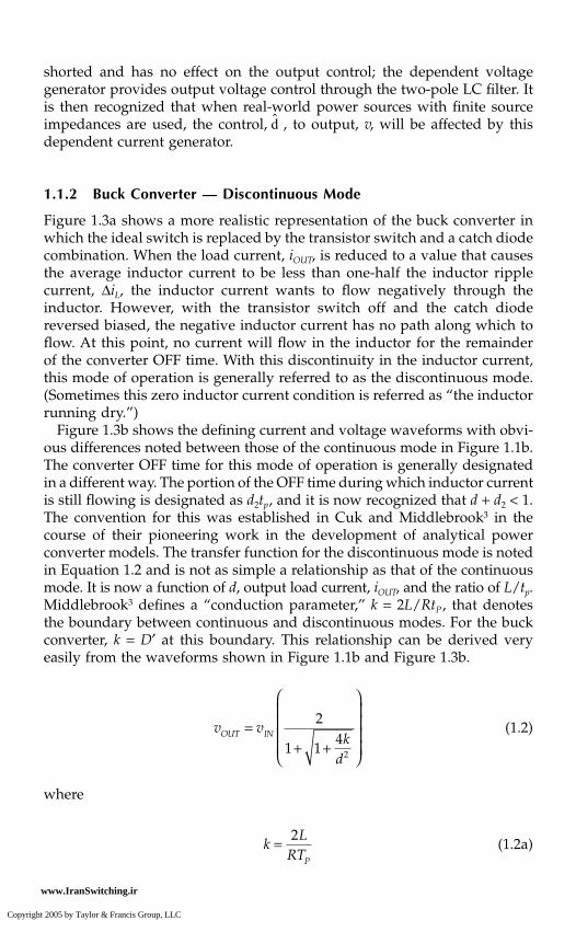
Power switch losses
. In a conventional PWM SMPS, these losses aregenerally thought of as saturation losses and switching losses. Thelatter occur during the finite transition time between the switchtransition from ON to OFF and vice versa. The saturation lossesoccur during the static part of the switching cycle. Figure 2.3 showsrepresentative periodic waveforms of voltage and currents in thesepower switches and the portions of the cycle, which attribute tosaturation or switching losses. Although rectifier diodes are not gen-erally thought of as switches, they do provide a switching functionand their power dissipations must be considered as a power switchloss.
•
Quiescent power losses
. These losses are consumed in the control andpower switch drive circuits and other miscellaneous peripheral cir-cuits. These miscellaneous circuits may exist as start-up supplies,power factor correction circuits, inrush current limiters, power mon-itoring circuits, and even external interface circuitry.
It would be nice if one could develop circuit-averaged models of the powerdissipation components of an SMPS that would be realistic enough to allowperforming the efficiency analysis entirely on the computer. Unfortunately,a wide diversity of “parasitic” circuit elements that have second- or third-order effects on the overall circuit must sometimes be considered. Also, they
DK_1137.book Page 23 Wednesday, June 15, 2005 11:49 AM
Copyright 2005 by Taylor & Francis Group, LLC
www.IranSwitching.ir
24
Practical Computer Analysis of Switch Mode Power Supplies
are generally difficult to quantify and model to the level of accuracy neces-sary to provide a reasonable estimation of the power supply efficiency. Thismakes it difficult to generalize about the best way to conduct an efficiencyanalysis of an SMPS.
Consider three ways of approaching this problem:
• Do a “hand–calculated” or spreadsheet type of tabulation of thelosses in the circuit. These loss effects may be determined frommanufacturer’s data sheets or from test data. Unfortunately, thisapproach is tedious and generally requires evaluation at many dif-ferent operating conditions.
FIGURE 2.3
Illustration showing power switch losses.
0 Watts
Saturation (or Conduction) Losses
PSWITCH
Turn On SwitchingTransition
SwitchingLosses
0 Amps
ON
OFF
ION
ISWITCH
0 Volts
VON
VSWITCH
Turn OffSwitchingTransition
DK_1137.book Page 24 Wednesday, June 15, 2005 11:49 AM
Copyright 2005 by Taylor & Francis Group, LLC
www.IranSwitching.ir

SMPS Analysis Requirements
25
• Develop a replicate exact switching circuit model that simulates theactual circuit and then compute the losses directly. This again requiresaccurate component models and may require a lot of “number-crunching” computing power if the power supply model is of anysignificant size. Also, the physical layout and wiring, which canaffect the switching action in an uncertain manner that is difficultto assess, must also be addressed.
• Develop an accurate large signal circuit-averaged model. This wouldbe a very desirable method and could possibly delineate from themodel that is developed for the analysis of other performanceparameters. Unfortunately, accurate large signal circuit-averagedcomponent loss parameters must be obtained and this may be verytedious and difficult, particularly in the case of the switching lossesof the power switches. The same physical problems as those in thepreceding case also apply for this switching loss case.
As might be surmised, there is no one easy way to calculate the efficiencyof an SMPS and obtain a level of accuracy that would be as good as anactual measurement. In the past, the first approach (the spreadsheet method)has been applied and will probably be the one most applied in the futureuntil advanced techniques are developed to allow other approaches such asthose proposed in the second and third bullets to be used to any extent. Ifonly a few dominant first-order conduction and switching losses are obvi-ous, the spreadsheet approach will provide the most practical determinationof efficiency.
2.1.4 Miscellaneous Range and Threshold Considerations
This area of analysis is sometimes overlooked but may be essential, especiallyfor problems that may exist during power-up and power-down of the SMPS.These problems may be in the form of inrush surge currents causing com-ponent stress conditions; power source overloading; output voltage over-shoot; or simply anomalous circuit operation, which may lead to componentdestruction, fuse blowing, or other malfunctioning effects. These thresholdanalyses may also apply for large load or line transients or even temporarypower dropouts that create operating conditions out of the normal range ofthe SMPS similar to those encountered during initial power-up. A largesignal (nonlinear) model containing the appropriate discontinuities must begenerated.
The situations encountered are somewhat complex to analyze (and design)because they involve sequential events that are functions of different thresh-old levels and time delays. Figure 2.4a and Figure 2.4b show a generalscenario of the sequence of events that may occur during initial power-up.This example is for a DC power source. An AC power source creates additionalconcerns because input rectification, filtering, and power factor correction
DK_1137.book Page 25 Wednesday, June 15, 2005 11:49 AM
Copyright 2005 by Taylor & Francis Group, LLC
www.IranSwitching.ir

26
Practical Computer Analysis of Switch Mode Power Supplies
provide added circuit complexity. In general, however, it is simply an exten-sion of the DC case. For now, consider the DC power source case.
The initial application of input voltage may be specified as a step functionor some function of time, such as a ramp, or maybe some nonlinear function.In any case, the design is required to accept this condition and analysis needsto verify this. A step input is probably the most typical and generally themost severe application of power if no severe voltage overshoots or sagsresult. The example in Figure 2.4a assumes this step input.
2.2 AC Requirements
Although most SMPSs provide a DC power conversion function, there are anumber of AC analysis concerns. The bulk of these issues involves control loopstability issues or noise-related issues such as electromagnetic compatibility.
FIGURE 2.4a
An example of an SMPS start-up scenario (circuit).
InrushSurgeLimiter
PWMConverter
InputFilter
VINVSOURCE
(ISOURCE)
VIN Level (With Hysteresis) orTime Delay Control
VREF
Soft StartControl
UVLOLevel
PWMControl
VREF
CONTROL CIRCUITS
VOUT
DK_1137.book Page 26 Wednesday, June 15, 2005 11:49 AM
Copyright 2005 by Taylor & Francis Group, LLC
www.IranSwitching.ir

SMPS Analysis Requirements
27
2.2.1 AC Control Loop Stability Margins
Of primary concern to the design of any feedback control circuit is the matterof AC control loop stability. In most cases, the verification of the desiredstability margin is achieved by showing that the Nyquist stability criterion
10,11
is satisfied. Other stability indicators, such as the Routh–Hurwitz
10,11
criteriaor perhaps some time domain criteria, may be applied, but in the vastmajority of cases, the linear techniques of the Nyquist criteria are appliedfor analysis and actual test verification.
FIGURE 2.4
bAn example of an SMPS start-up scenario (waveforms).
VSOURCE
0 Volts
0 Amps
VREF
VOUT
0 Volts
0 Volts
VIN
Inrush LimiterSwitched Out Here
ISOURCE
Threshold of Regulation
VREF
Soft Start Control
DK_1137.book Page 27 Wednesday, June 15, 2005 11:49 AM
Copyright 2005 by Taylor & Francis Group, LLC
www.IranSwitching.ir

28
Practical Computer Analysis of Switch Mode Power Supplies
The classical Nyquist plot is a polar plot of loop gain vs. loop phase withfrequency the independent variable. The criteria’s goal is to show that nopositive real roots occur in the characteristic equation of the closed looptransfer function.
10,11
Figure 2.5a shows a simple feedback control circuit andFigure 2.5b shows a Nyquist plot representation of the loop gain and phase.The basic criterion for stability states that this plot must not encircle the –1,–180
°
coordinate. The degree of stability is provided by the phase margin,
φ
M
, which is the loop phase angle occurring at the unity loop gain crossoverpoint, and the gain margin, which is the loop gain at the –180
°
loop phasepoint.
The most practical and conventional representation of this criterion is,however, in the form of the Bode plot shown in Figure 2.5c. This is a semilogplot of loop gain, expressed in decibels, vs. frequency and another plot ofloop phase vs. frequency. It contains basically the same information as thatof the classical Nyquist plot but allows a much simpler way of plotting,analyzing, and interpreting the results. Analyzing feedback loops is one ofthe more interesting challenges of an SMPS analysis or any linear controlsystem for that matter. See Middlebrook’s very good paper
12
on dealing withthe concepts of multiple loop regulation systems.
FIGURE 2.5a
Basic SMPS feedback control circuit.
RLOAD
vOUT
VREF
-
+
Power StageGain (H)
v1
v2
v3
FeedbackRegulation
Loop
DK_1137.book Page 28 Wednesday, June 15, 2005 11:49 AM
Copyright 2005 by Taylor & Francis Group, LLC
www.IranSwitching.ir

SMPS Analysis Requirements
29
FIGURE 2.5b
Nyquist plot of loop gain.
FIGURE 2.5c
Bode plot of loop gain and phase.
- 270oGM
(Gain Margin)
(Phase Margin)
0o
LoopPhase
LoopGain
PhaseShift
(-1,- 180o)
- 180o
IncreasingFrequency
MΦ
0 dB
0o
-90o
-270o
-180o
GM
Log FreqLoop Gain
Loop Phase
MΦ
DK_1137.book Page 29 Wednesday, June 15, 2005 11:49 AM
Copyright 2005 by Taylor & Francis Group, LLC
www.IranSwitching.ir

30
Practical Computer Analysis of Switch Mode Power Supplies
2.2.2 Input Filter Stability Margins
Most SMPSs have a low-pass input filter; this is required for a number ofreasons, but in essence it provides noise isolation between the power sourceand the SMPS. (See Appendix A for a detailed synopsis of SMPS input filters.)Unfortunately, the insertion of this filter has some undesirable effects oncircuit performance. One of the most serious is that this filter has the capa-bility of producing an AC instability on the input voltage line presented tothe power converter. The reason for this is that the SMPS presents a constantpower load to the source and input filter and, because it is a constant powerload, it has a negative incremental resistance characteristic (Figure 2.6). Whenconsidered as a negative resistance load connected to the equivalent parallelresonant circuit of the input filter, it can negate any “small” positive resis-tances in the input circuit and produce a classical electronic oscillator.
Middlebrook and Cuk
2
and Middlebrook
13
offer very good treatments ofthis subject and provide information on dealing with voltage mode con-verters. These are generally more complex to optimize than current modeconverters because the AC input impedance of the voltage mode convertercan have a considerable variation with frequency, particularly at the lower
FIGURE 2.6
Negative resistance loading on SMPS input filter.
V∆I∆
VIN
IIN
Constant Power Load
V
I
=∆∆
IV Negative
IncrementalResistance
DK_1137.book Page 30 Wednesday, June 15, 2005 11:49 AM
Copyright 2005 by Taylor & Francis Group, LLC
www.IranSwitching.ir

SMPS Analysis Requirements
31
frequencies near the resonant frequencies of the input and output filters. Thecurrent mode converter input impedance, on the other hand, is generallyconsidered constant up to the loop gain crossover frequency of the innercurrent loop.
12
Figure 2.7 shows representative SMPS regulator input imped-ance plots illustrating this comparison. With this relatively constant negativeinput impedance throughout the lower frequencies, the current mode con-verter input filter problem is generally an easier and more straightforwardissue with which to deal.
The solution to this problem is to insert additional damping elements inthe input filter; these alter the circuit to the extent that the negative resistancecomponent of the resonant circuit is negated and the net resistance is posi-tive. At the same time, it is vital that the necessary compromises for stabilitydo not reduce the performance of the input filter to the point at which itsrequirements are not met. Middlebrook and Cuk
2
show a number of differentdamping circuit approaches that may be taken. The main generalized con-clusion is that the parallel resonant peak output impedance of the input filterpresented to the SMPS should be at least three times less than the inputimpedance of the SMPS. This not only ensures AC stability but also negatesany potential adverse effects on SMPS performance. These negative effects
FIGURE 2.7
Typical SMPS source/load impedance comparison.
Current Mode SMPS RegulatorInput Impedance (Load)
Log Freq
Output Impedanceof Input Filter
(Source) Voltage Mode SMPSRegulator Input Impedance
(Load)
dB
0 dB
DK_1137.book Page 31 Wednesday, June 15, 2005 11:49 AM
Copyright 2005 by Taylor & Francis Group, LLC
www.IranSwitching.ir

32
Practical Computer Analysis of Switch Mode Power Supplies
are manifested in voltage mode converters as an effective loop gain reduc-tion. This could cause a reduction in line noise rejection by the regulator andalso a possible increase in output impedance. Multiple stage filters are some-times necessary to meet the requirements. See Appendix A for a generaltreatment of input filter circuit design.
2.2.3 Source and Load Stability Margins
The concerns pertaining to this subject are simply a further application ofthe impedance-matching criteria noted in the previous section. It is essentialfor power system AC stability to analyze any system containing a numberof SMPSs to ensure that these impedance-matching criteria are not violated.Systems that consist of a large central SMPS regulator and several smallerpost switching regulators, and even a postmagnetic amplifier, need to beanalyzed. It may take a lot of computer modeling to analyze a systemcontaining several SMPSs accurately.
2.2.4 Electromagnetic Compatibility
When an accurate model of the power supply, along with its input filter,is created, the electromagnetic compatibility (EMC) performance aspectsare easily analyzed. The general list of items relegated to this categorycomprises:
•
Conducted susceptibility
. This analysis is to ensure that specified levelsof noise interference on the input power lines do not cause anyappreciable degradation of SMPS performance. This responserequirement is generally specified as an AC sine wave voltage addedto the normal input power lines at various voltage amplitudes overvarious frequency bands. The frequency bands may start as low as30 Hz and extend into the megahertz region. Also, these input ACnoise sources may be differential or common mode. Various tran-sient phenomena such as line spikes with specified pulse shapes andenergy content also need to be analyzed. (Ott
15
provides very goodgeneral reference source materials for almost any EMC concern asso-ciated with electronic equipment.)
•
Conducted emissions
. This analysis is to ensure that an acceptable levelof conducted current noise emanating from the SMPS and goingback to the power source will not be exceeded. This current may bedifferential and/or common mode. Load current perturbationsreflected back through the SMPS to the source are also to be consid-ered. In many cases, a transient time domain analysis is necessaryfor these emission analyses.
DK_1137.book Page 32 Wednesday, June 15, 2005 11:49 AM
Copyright 2005 by Taylor & Francis Group, LLC
www.IranSwitching.ir

SMPS Analysis Requirements
33
In all probability, radiated susceptibility and radiated emission require-ments will need to be met. The analysis required for this generally exists inthe area of electromagnetic fields analysis. This is not specifically consideredin this book, but might be considered if conducted effects are determined toresult from the presence of these fields.
2.3 Transient Requirements
The transient performance requirements of an SMPS generally exist in theform of specifying a limit for output voltage variations with line voltageand/or load current perturbations. A circuit-averaged model or the actualtime domain model may be necessary for these transient analyses. The exam-ples of Chapter 4 and Chapter 6 provide considerable general treatment ofthese effects.
2.3.1 Load Transients
Load current transients are one of the most commonly specified stimuli forany power supply. Load current perturbations may occur in all sorts of ways,such as single-event load changes or steady-state periodic load changes (e.g.,pulse trains and sinusoidal wave shapes, etc.). The single-event load changesare in general the turn-on (and turn-off) load surges of equipment poweredby the power supply. The magnitude of some of these changes may be smallenough that the SMPS stays within its existing operating mode, or it maybe large enough to traverse the continuous–discontinuous mode conditionboundary. Still other load changes may be large enough to send the powersupply into a current limit mode. Output short-circuit conditions may needto be analyzed if this is a requirement. An accurate large signal model isrequired to analyze all of these various modes of operation.
2.3.2 Line Transients
Input line voltage transients are also very commonly specified stimulifor a power supply. These transients may be single-event voltage changesand also steady-state periodic pulse trains. The crossing of the SMPScontinuous–discontinuous conduction mode boundary may occur forsome transients. These transients may in many cases be specified as partof an EMC specification (see Section 2.2.4) or they may be specified in aseparate listing of requirements. In any case, SMPS performance must beanalyzed for all conditions.
DK_1137.book Page 33 Wednesday, June 15, 2005 11:49 AM
Copyright 2005 by Taylor & Francis Group, LLC
www.IranSwitching.ir

34
Practical Computer Analysis of Switch Mode Power Supplies
2.3.3 Power-Up and Power-Down Transients
Power-up and power-down transients are considered a special case ofinput line voltage transients. The input voltage may be applied as a stepfunction resulting from a relay or switch closure, with the possibility ofa sag in input voltage caused by large SMPS inrush currents and finitepower source impedances. This could cause problems with undervoltagelockout circuits, inrush current-limiting circuits, and even “housekeep-ing” power supplies. On the other hand, a slow rising ramp or someother voltage profile caused by a slow source power generator start-upcould cause anomalous start-up SMPS problems, which may even bedestructive. Many times, this type of problem is discovered and dealtwith in the lab experimentally; however, an accurate SMPS model alongwith the computer analysis may help in providing valuable insight anda solution when it is difficult to make an assessment of the actual circuitoperation. Sometimes, power-down can cause the same problems, inreverse, as those for power-up; anomalous destructive circuit operationoccurs. (See Section 2.1.4 for more general information on a typicalpower-up sequence of events.)
2.3.4 Energy Storage for Line Dropouts
Line dropouts that require external components to be brought into play tomaintain SMPS performance requirements are also considered a special caseof transient operation. When these dropouts occur and continued outputpower to the loads is required, a back-up power source is necessary. Thispower source may be required to provide power for short transitory periodsthat are only a little longer than the energy storage capability of the SMPSfilter capacitors, or the requirement may be for longer periods of time, whichwould suggest a near steady or continuous type of operation. The energystorage for shorter periods of time is generally provided by a charged-upcapacitor bank, but for longer periods of time, a back-up battery may benecessary. These types of backup are generally referred to as uninterruptablepower supplies (UPSs).
In most cases, when a battery back-up is used, a simple diode ORing ofthe two supplies is all that is required; little or no special analysis is neededfor this case. When a charged-up capacitor bank is used for the shorter timeperiod dropouts, the situation generally becomes a little more complex. Thecapacitor bank is charged to a higher voltage than that of the input voltagefor adequate energy storage. When this is done, it becomes necessary tocontrol or regulate the discharging of these capacitors onto the input powerlines. To ensure adequate SMPS performance, an analysis of this conditionis necessary. This capacitor bank scenario may be implemented on any orall of the output power lines as well.
DK_1137.book Page 34 Wednesday, June 15, 2005 11:49 AM
Copyright 2005 by Taylor & Francis Group, LLC
www.IranSwitching.ir

SMPS Analysis Requirements
35
2.4 Summary
This chapter has attempted to present most of the fundamental analysis tasksthat may be required to verify the design integrity of a power supply. Therequirements presented are by no means all inclusive; many other specializedrequirements may need to be analyzed. In any case, it is the intent of thischapter to emphasize the importance of identifying all of the necessary anal-ysis requirements for a particular power supply. The succeeding chapters willpresent the methods available to the analyst to facilitate a practical computeranalysis of the power supply to verify that the requirements are met.
DK_1137.book Page 35 Wednesday, June 15, 2005 11:49 AM
Copyright 2005 by Taylor & Francis Group, LLC
www.IranSwitching.ir

37
3
Fundamental Switch Mode Converter
Model Development
This chapter develops the fundamental models necessary to analyze theessential requirements of switch mode power supplies (SMPSs) as noted inChapter 2. The large signal continuous and discontinuous mode models forthe buck and the boost converters are developed. Then the continuous anddiscontinuous mode models are integrated into a single unified model foreach of the buck and boost converters. The unified buck–boost (conventionalflyback converter) and Cuk converter models are next developed. After thedevelopment of these models, an example analysis is provided to illustratethe ease and simplicity that this approach affords in analyzing the perfor-mance of SMPSs.
3.1 Buck and Boost Converter Continuous ModeLarge Signal Models
When a switch mode power converter is modeled, an electrical circuit equiv-alent model of the duty ratio controller must be created when the converteroperates in the continuous mode. From Middlebrook and Cuk,
1
an ideal (ACand DC) transformer equivalent model is conceived and shown in Figure 3.1.The flyback and Cuk converter continuous mode models are in essencecascaded versions of the buck and boost converters and will be dealt withlater.
Converting the ideal transformers to a system of dependent generatorsmakes the models more adaptable to most circuit simulation software.Figure 3.2 shows a SPICE model equivalent. The power converter largesignal continuous mode models are thus implemented in Figure 3.3. See Cukand Middlebrook
4
for more information.
DK_1137.book Page 37 Wednesday, June 15, 2005 11:49 AM
Copyright 2005 by Taylor & Francis Group, LLC
www.IranSwitching.ir

38
Practical Computer Analysis of Switch Mode Power Supplies
3.2 Buck and Boost Converter Discontinuous ModeLarge Signal Models
Now consider the discontinuous mode of operation. From Figure 3.4, theaverage discontinuous mode inductor current,
i
LD
, is expressed by:
(3.1)
FIGURE 3.1
Duty ratio controller ideal transformer.
FIGURE 3.2
Ideal transformer equivalent model.
a) Buck Converter
d C R
Ld’
C
R
+
vg
d : 1
..
L
b) Boost Converter
=
=vg
d
d’
L
C R
L
C
R
+
vg
1 : d
. .+
vg
+
iI
d dLDP= +2 2( )
i3,4
=
+
+1 : d
. .
1
2
3
4
1 3
2 4
F = d x i3,4
E = d x v1,2
VM = 0
i3,4
DK_1137.book Page 38 Wednesday, June 15, 2005 11:49 AM
Copyright 2005 by Taylor & Francis Group, LLC
www.IranSwitching.ir

Fundamental Switch Mode Converter Model Development
39
For the buck converter,
(3.2)
FIGURE 3.3
Power converter continuous mode models.
FIGURE 3.4
Discontinuous mode inductor current.
a) Buck Converter
+
+F = d x iLC
E = d x vg
VM = 0
L
C
R
+
vg
v
iLC
b) Boost Converter
F = d’ x iLC
C
R
+
vg
+
+
E = d’ x v
VM = 0
Lv
iLC
Iv v dT
LPg S=
−( )
d2TPdTP
TP
iLDIP
0
DK_1137.book Page 39 Wednesday, June 15, 2005 11:49 AM
Copyright 2005 by Taylor & Francis Group, LLC
www.IranSwitching.ir

40
Practical Computer Analysis of Switch Mode Power Supplies
Also, for periodic volt-second balance across the inductor,
or
(3.3)
Substituting Equation 3.2 and Equation 3.3 into Equation 3.1 yields thedesired control equation for the buck converter,
i
LD
:
(3.4)
For the boost converter,
(3.5)
and for volt-second balance
(3.6)
Substituting Equation 3.5 and Equation 3.6 into Equation 3.1 yields thecontrol equation for the boost converter,
i
LD
:
(3.7)
The next step is to develop a large signal discontinuous mode model fromthe previous equations. Figure 3.5 shows buck and boost topologies.
The terms
i
LID
and
i
LOD
are as yet undefined. With the inductor currentstarting and returning to zero during each cycle, there is no cyclical energystorage in the inductor. Its properties as an inductive circuit element arenonexistent at the lower frequencies; therefore it does not appear in themodels.
d v v d vg( )− = 2
d dv v
vg
2 =−⎛
⎝⎜
⎞
⎠⎟
i dv
vv v
TLLD
gg
s= −2
2( )
Iv dT
LPg s=
dv d v vg g= −2( )
d dv
v vg
g2 =
−
⎛
⎝⎜⎜
⎞
⎠⎟⎟
i dvv
v vTLLD
g
g
S=−
⎛
⎝⎜⎜
⎞
⎠⎟⎟
2
2
DK_1137.book Page 40 Wednesday, June 15, 2005 11:49 AM
Copyright 2005 by Taylor & Francis Group, LLC
www.IranSwitching.ir

Fundamental Switch Mode Converter Model Development
41
With this knowledge, the instantaneous or cyclical power into the converteris equal to the instantaneous power out.
(3.8)
For the buck converter,
(3.9)
(3.10)
and
(3.11)
For the boost converter,
(3.12)
(3.13)
FIGURE 3.5
Discontinuous mode large signal models.
iLDiLIDC
R
v
vg +
a) Buck Converter
iLODC
R
v
vg +iLD
b) Boost Converter
p pin out=
p v iin g LID=
p viout LD=
ivv
iLIDg
LD=
p v iin g LD=
p viout LOD=
DK_1137.book Page 41 Wednesday, June 15, 2005 11:49 AM
Copyright 2005 by Taylor & Francis Group, LLC
www.IranSwitching.ir

42
Practical Computer Analysis of Switch Mode Power Supplies
and
(3.14)
Current
i
LID
is the correct input current for the buck converter and
i
LOD
isthe correct output current for the boost converter.
3.3 Buck and Boost Continuous and DiscontinuousMode Unified Models
Now combine the continuous and discontinuous mode models into oneencompassing unified model, which will emulate an actual converter goingfrom one conduction mode to the other as the critical inductor currentboundary is traversed. The schemes depicted in Figure 3.6 and Figure 3.7provide a simple and straightforward way of implementing this model.
A detailed explanation of this topology is now in order. For the moment,ignore the center components of Figure 3.6 consisting of VM2, D1, D2,
i
LID
,and F1. The discontinuous mode current,
i
LD
, is calculated for all prevailingconditions of
d
,
v
g
, and
v
according to Equation 3.4. If the voltage,
E
, issufficiently high to produce an inductor current larger than the value of
i
LD
,diode D3 will then conduct. (Diode D3 is modeled as an ideal diode with aforward voltage drop near 0 V. Section 3.10 discusses this further.) Theconverter is thus in the
continuous
mode with
i
L
>
i
LD
. D3 basically shorts outcurrent source
i
LD
, thus making it appear as though it is not in the circuit.
FIGURE 3.6
Buck converter combined continuous and discontinuous mode model.
iv
viLOD
gLD=
+
+
+
+V
D1
D2
iLID
iLD
E = d x vg
VM1 = 0V
VM2 = 1V F1 = d x iLF2 = ib
iL
L
ibvg
C
R
D3
DK_1137.book Page 42 Wednesday, June 15, 2005 11:49 AM
Copyright 2005 by Taylor & Francis Group, LLC
www.IranSwitching.ir

Fundamental Switch Mode Converter Model Development
43
This is appropriate because
i
LD
is a nonexistent fictitious quantity for
i
L
greater than any computed quantity greater than
i
LD
. If circuit conditionschange to lower
i
L
so that
i
L
wants to be less than
i
LD
, D3 will be reversedbiased and the actual inductor current will be
i
LD
. The converter is now inthe discontinuous mode with
i
L
=
i
LD
. Now consider the role of the components VM2, D1, D2,
i
LID
, and F1 thatwere ignored earlier. The circuit made from these components is necessaryto provide the proper input current that is seen as a load on the powersource
v
g
. The circuit is basically a current ORing circuit, with current
i
b
equal to the larger of the two currents F1 or
i
LID
. For example, if current F1 islarger than
i
LID
, nonideal diode D1 will conduct, effectively shorting out
i
LID
,and D2 is reversed biased with
i
b
=
F1. This is the continuous mode case withF2
=
i
b
=
F1
=
d
×
i
L
, which is the correct converter input current in thecontinuous mode. If current F1 decreases below the computed discontinuousmode current,
i
LID
, then
i
b
will be equal to
i
LID
, which is the correct discontin-uous mode current.
Voltage source VM2 is shown in Figure 3.6 as 1 V, but may be any arbitrarypositive value. When a value greater than zero is used for VM2, the voltageat the cathode side of diode D2 will have basically one of two values,depending on the converter conduction mode. This circuit may now also beviewed as a conduction mode detector circuit when monitoring the voltageat the D2 cathode.
Thus, the complete unified continuous and discontinuous mode modelfor the buck converter is shown in Figure 3.6. It can be recognized fromFigure 3.3 and Figure 3.5 that the buck and boost topologies are in essencethe duals of each other; therefore, it can be easily deduced that the modelshown in Figure 3.7 is the correct unified model for the boost topologyby applying the corresponding line of development as for the buck con-verter.
FIGURE 3.7
Boost converter combined continuous and discontinuous mode model.
+
V
F2 = ib
vg
C
R+ +
+
D1
D2
iLOD
iLD
E = d’ x vg
VM1 = 0V
VM2 = 1VF1 = d’ x iL
iL
L
ib
D3
DK_1137.book Page 43 Wednesday, June 15, 2005 11:49 AM
Copyright 2005 by Taylor & Francis Group, LLC
www.IranSwitching.ir

44
Practical Computer Analysis of Switch Mode Power Supplies
3.4 Buck–Boost (Flyback) Converter ContinuousMode Large Signal Model
The buck–boost converter is in essence a cascaded combination of the buckand boost converters (Figure 3.1a and Figure 3.1b, respectively). Figure 3.8shows an equivalent representation of this combination. (See Cuk andMiddlebrook
4
for more detail on this.) Replacing the duty ratio controllingswitches with their equivalent circuit models as developed in Section 3.1,the equivalent continuous mode model is shown in Figure 3.9.
3.5 Buck–Boost (Flyback) Converter DiscontinuousMode Large Signal Model
From the inductor current
waveform of Figure 3.4, Equation 3.1, and thefollowing equations, the average discontinuous mode current,
i
LD
, is deter-mined from Figure 3.8.
(3.15)
FIGURE 3.8
Basic buck–boost (flyback) converter continuous mode topology.
FIGURE 3.9
Buck–boost (flyback) continuous mode model.
d C R
Ld’
vg
d
d’+
v
Iv dT
LPg s=
+
+F1 = d x iLC
E1 = d x vg
VM1 = 0
+vg
R
+
+
E3 = d’ x v
VM3 = 0
L
F3 = d’ x iLC
C
v
iLC
DK_1137.book Page 44 Wednesday, June 15, 2005 11:49 AM
Copyright 2005 by Taylor & Francis Group, LLC
www.IranSwitching.ir

Fundamental Switch Mode Converter Model Development
45
Also,
or
(3.16)
Substituting Equation 3.15 and Equation 3.16 into Equation 3.1 yields thedesired control equation for the flyback converter:
(3.17)
When the flyback converter is modeled only in the discontinuous mode,the average inductor current, i
LD
, as indicated in Equation 3.17 is not essen-tial, as shown in Figure 3.10. However, its necessity will be noted whendeveloping the unified model. The equations for
i
LID
and
i
LOD
are easily notedfrom Figure 3.4 and Equation 3.15 and Equation 3.16.
(3.18)
and
(3.19)
FIGURE 3.10
Flyback discontinuous mode model.
dv d vg = 2
d dv
vg
2 =
i d vv
vTLLD g
g s= +⎛
⎝⎜
⎞
⎠⎟2 1
2
iI
dLIDP=2
i d vTLLID gs= 2
2
iI
dLODP=2 2
i dv
vTLLOD
g S=⎛
⎝⎜⎜
⎞
⎠⎟⎟
22
2
iLD
v
iLIDvg +iLOD
C
R
(Transparent)
DK_1137.book Page 45 Wednesday, June 15, 2005 11:49 AM
Copyright 2005 by Taylor & Francis Group, LLC
www.IranSwitching.ir

46P
ractical Com
puter Analysis of Sw
itch Mode P
ower Supplies
FIGURE 3.11Flyback converter continuous and discontinuous mode model.
V
= 4F i Ob
C
R+ +
+
4D
5D
i OL D
d = 2E ’ v x
MV 0 = 3 V
MV 1 = 4 V3F i x ’d = L
i Ob
+
+
+
+
1D
2D
i DIL
i DL
d = 1E v x g
MV V0 = 1
2MV V1 = F1 d = i x L= 2F i Ib
iL
L
i Ib
vg
5D
DK
_1137.book Page 46 Wednesday, June 15, 2005 11:49 A
M
Copyright 2005 by T
aylor & Francis G
roup, LL
C
www.IranSwitching.ir
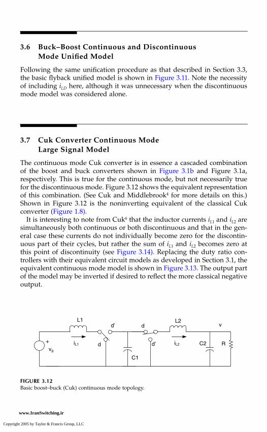
Fundamental Switch Mode Converter Model Development 47
3.6 Buck–Boost Continuous and DiscontinuousMode Unified Model
Following the same unification procedure as that described in Section 3.3,the basic flyback unified model is shown in Figure 3.11. Note the necessityof including iLD here, although it was unnecessary when the discontinuousmode model was considered alone.
3.7 Cuk Converter Continuous ModeLarge Signal Model
The continuous mode Cuk converter is in essence a cascaded combinationof the boost and buck converters shown in Figure 3.1b and Figure 3.1a,respectively. This is true for the continuous mode, but not necessarily truefor the discontinuous mode. Figure 3.12 shows the equivalent representationof this combination. (See Cuk and Middlebrook4 for more details on this.)Shown in Figure 3.12 is the noninverting equivalent of the classical Cukconverter (Figure 1.8).
It is interesting to note from Cuk6 that the inductor currents iL1 and iL2 aresimultaneously both continuous or both discontinuous and that in the gen-eral case these currents do not individually become zero for the discontin-uous part of their cycles, but rather the sum of iL1 and iL2 becomes zero atthis point of discontinuity (see Figure 3.14). Replacing the duty ratio con-trollers with their equivalent circuit models as developed in Section 3.1, theequivalent continuous mode model is shown in Figure 3.13. The output partof the model may be inverted if desired to reflect the more classical negativeoutput.
FIGURE 3.12Basic boost–buck (Cuk) continuous mode topology.
d C2 R
L1d’
vg
d
+
v
d’
L2
C1
iL1 iL2
DK_1137.book Page 47 Wednesday, June 15, 2005 11:49 AM
Copyright 2005 by Taylor & Francis Group, LLC
www.IranSwitching.ir

48 Practical Computer Analysis of Switch Mode Power Supplies
3.8 Cuk Converter Discontinuous Mode Large Signal Model
From the inductor current waveforms of Figure 3.14 and the following equa-tions, the average discontinuous mode inductor currents iL1D and iL2D aredetermined from the circuit of Figure 3.12:
(3.20)
FIGURE 3.13Boost–buck (Cuk) continuous mode topology.
FIGURE 3.14Cuk converter discontinuous mode inductor currents.
F1 = d x iL1
E1 = d x vC
VM1 = 0V
+vg
R
E2 = d’ x vC
L2
F2 = d’ x iL2
C
iL2
+
+
L1
+
+VM2 = 0V
v
iL1
C1
vC
iI
d d iL DP
11
22= + +( )
IP2
iL2D
IP1
0 V
iL1D
0 V
d2TSdTS
TS
+ i
- i
DK_1137.book Page 48 Wednesday, June 15, 2005 11:49 AM
Copyright 2005 by Taylor & Francis Group, LLC
www.IranSwitching.ir

Fundamental Switch Mode Converter Model Development 49
(3.21)
where
(3.22)
and
(3.23)
For cyclical volt-second balance across L1 and L2,
(3.24)
and
(3.25)
Eliminating vc from Equation 3.24 and Equation 3.25 yields
(3.26)
Now, combining Equation 3.20 through Equation 3.26 yields
(3.27)
and
(3.28)
From Cuk and Middlebrook,3
(3.29)
iI
d d iL DP
22
22= + −( )
Iv dT
LPg s
11
=
Ivd T
LPs
22
2
=
dv d v vg c g= −2( )
d v d v vc2 = −( )
d dv
vg
2 =
i v dv
vTL
iL D gg s
12
1
12
= +⎛
⎝⎜
⎞
⎠⎟ +
i v dv
vTL
iL D gg s
22
2
12
= +⎛
⎝⎜
⎞
⎠⎟ −
i iL L
L LL D
vgv=
−+21 2
1 2
DK_1137.book Page 49 Wednesday, June 15, 2005 11:49 AM
Copyright 2005 by Taylor & Francis Group, LLC
www.IranSwitching.ir

50 Practical Computer Analysis of Switch Mode Power Supplies
and with cyclical input power equal to cyclical output power,
(3.30)
and
(3.31)
Substituting Equation 3.31 into Equation 3.25 and solving for iL1D yields
(3.32)
where
The discontinuous mode noninverting Cuk converter model is then simplyshown in Figure 3.15 with iL1D indicated by Equation 3.32 and iL2D indicatedby Equation 3.30.
3.9 Cuk Converter Continuous and DiscontinuousMode Unified Model
Again, following the same unification procedure as described in Section 3.3,the basic Cuk converter unified model is shown in Figure 3.16. Note that theoutput stage may be inverted for a positive or a negative output.
FIGURE 3.15Cuk converter (noninverting) discontinuous mode large signal model.
iL1DC
R
v
vg +iL2D
i iv
vL D L Dg
2 1=
i iL L
L LL D
vgv=
−+1
1 2
1 2
i v dTLL D gs
e1
2
2=
LL L
L Le =+1 2
1 2
DK_1137.book Page 50 Wednesday, June 15, 2005 11:49 AM
Copyright 2005 by Taylor & Francis Group, LLC
www.IranSwitching.ir

Fundamental Sw
itch Mode C
onverter Model D
evelopment
51
FIGURE 3.16Cuk converter continuous and discontinuous mode model.
vC
F3 = d x ibO
C1
F2 = d’ x ibI
+
vg+ +
+
D1
D2
iL1OD
E1 = d’ x vC
VM1 = 0V
VM2 = 1VF1 = iL1
iL1
ibI
+
+
+V
D3
D4
iL2ID
E2 = d x vC
VM4 = 0V
VM3 = 1V F4 = iL2
iL2
ibO
C2
R
L1
iL1D
D5
iL2D
D6
L2
DK
_1137.book Page 51 Wednesday, June 15, 2005 11:49 A
M
Copyright 2005 by T
aylor & Francis G
roup, LL
C
www.IranSwitching.ir

52 Practical Computer Analysis of Switch Mode Power Supplies
3.10 Boost Converter Model Analysis Example
Now create a model of a boost converter as an example to illustrate the easeand simplicity of the technique. Consider the duty ratio controlled boostconverter of Figure 3.17 operating in the constant frequency mode of 75 kHz(a period of Ts = 13.33 µsec).
An equivalent unified PSPICE model is derived from Figure 3.7 and shownin Figure 3.18. The diode, DIDEAL, is modeled as an ideal diode with thecharacteristics shown in Figure 3.19. This ideal diode model uses VF = −1 µVas opposed to a desired value of zero because, in some applications, a zerovalue could be divided into other factors, thus causing the simulation tocrash. This model does not allow this situation and VF is small enough thatthe diode is considered ideal. The ideal diode is here simply generated bya dependent voltage generator and a table function. (See the circuit netlistsin Figure 3.22 and Figure 3.23.) In later chapters, netlists will show otherways of creating this ideal diode. If a simulation convergence problem exists,trying a different type of model creation may sometimes help.
The equations for iLD and iLOD are obtained from Equation 3.7 and Equa-tion 3.14, respectively.
(3.33)
FIGURE 3.17Duty ratio controlled boost converter example.
i dv
LD vvg
=−
⎛
⎝⎜⎜
⎞
⎠⎟⎟
0 0171
2.
0.3 A
0 A
d
d′
+
L390 µH
R(825 Ω, 75 Ω)
C24 µC
vg
LoadCurrent
Pulse
5 mSec
DK_1137.book Page 52 Wednesday, June 15, 2005 11:49 AM
Copyright 2005 by Taylor & Francis Group, LLC
www.IranSwitching.ir

Fundamental Switch Mode Converter Model Development 53
and
(3.34)
Care must be taken in this simulation that v does not drop below vg becausea division by zero may result in Equation 3.33 and cause the simulation tocrash. Although not used here, a LIMIT function may be used in the modelequation for GILD to prevent this if convergence trouble is encountered. (Seethe netlists in Figure 3.22 and Figure 3.23).
The steady state critical inductor current (average inductor current at theboundary between the continuous and discontinuous modes of operation)
FIGURE 3.18Boost converter PSPICE unified model.
VDAC1
+
VDDC0.55
9
+10 11
0
RD1
VD11
(d’)
F21
++ +
+
D1
D2
iLOD
E = d’ x v
VM1 = 0V
VM2 = 0VG1(d’ x iL)
iL
ib
L 390 µH
(iLD)5
8
VGDC11.25
VGAC
XD1DIDEAL
7GILD
v
6
4
3
2
1
0
R (825 Ω, 75 Ω)
ILOAD(Transient
Analysis Only)
C24 µF
+
+
iv
viLOD
gLD=
DK_1137.book Page 53 Wednesday, June 15, 2005 11:49 AM
Copyright 2005 by Taylor & Francis Group, LLC
www.IranSwitching.ir

54 Practical Computer Analysis of Switch Mode Power Supplies
for this example occurs at
(3.35)
or
(3.36)
Three tests will be conducted on the model to reveal some of its charac-teristics. The first will show the AC response from the duty controller, d, tothe output voltage, v, with the converter operating in the continuous mode(R < RCRIT) for R = 75 Ω. Then, for the second test, the load resistor will beincreased from 75 to 825 Ω, placing the converter in the deep discontinuousmode and examining the AC response under that condition. The third testwill be to examine the effect on output voltage of a transient load current
FIGURE 3.19“Ideal” diode characteristics.
I
V0
VF = -1.0 µV
IV DT
LV S
CRITg s= =2
11 25 0 55 13 332 390
( . )( . )( . )(
µµHH
A)
.= 0 106
RV
D IV
ACRITCRIT
=′
= =250 45 0 106
524( . )( . )
Ω
DK_1137.book Page 54 Wednesday, June 15, 2005 11:49 AM
Copyright 2005 by Taylor & Francis Group, LLC
www.IranSwitching.ir

Fundamental Switch Mode Converter Model Development 55
pulse on the converter forcing it to move from the discontinuous mode(R = 825 Ω) to the continuous mode and back again with a load current pulseof 0.3 A lasting for 5 msec.
The results of these tests are shown in Figure 3.20 and Figure 3.21. Notethe characteristic right-half plane zero for the continuous mode in Figure 3.20.Note that the discontinuous mode AC response of Figure 3.20 is of consid-erably lower bandwidth with a single pole roll-off and also the absence of
FIGURE 3.20Boost converter AC analysis example.
FIGURE 3.21Boost converter load transient analysis example.
60
0d
100 Hz 1.0 KHzFrequency
10 KHz 100 KHz
4020
0−20
−60
−90d
−180d
−270d
P(V (1))
DB(V(1))
GEL
>>
Discontinuous Mode Gain (Rout = 825)
Continuous Mode Gain (Rout = 75)
Discontinuous Mode Phase (Rout = 825)
Continuous Mode Phase (Rout = 75)
40 V
30 V
20 V
0 A0 µ 5 mn 10 mn 15 mn
Time20 mn 25 mn 30 mn
GEL
>>
V(1)
I (ILOAD)
Continuous Mode Underdamped Ringing
?
?
DK_1137.book Page 55 Wednesday, June 15, 2005 11:49 AM
Copyright 2005 by Taylor & Francis Group, LLC
www.IranSwitching.ir

56 Practical Computer Analysis of Switch Mode Power Supplies
the right-half plane zero. Now observe the results of the load transient testin Figure 3.21. Note that the predictable large signal result of the outputvoltage, v, varies considerably when the inductor current is less than itscritical value of 0.106 A. Also note the expected underdamped ringingaround the continuous mode output voltage value of 25 V.
Numerous other tests — possibly more practical ones — could be easilydevised and conducted on the model to examine easily any large signaltransient or small AC characteristic desired. For reference, the PSPICE™netlists for the AC and transient analysis are shown in Figure 3.22 andFigure 3.23, respectively.
Boost Converter AC AnalysisVGDC 8 0 DC 11.25VGAC 7 8 AC 0L 7 6 390UGILD 6 5 VALUE = (0.017)*PWR(-V(10),2)*(V(1)/((V(1)/V(7))-1))XD1 6 5 DIDEAL**Ideal Diode Model.SUBCKT DIDEAL 1 2EID 3 1 TABLE [V(3,2)] = (-1,1U)(0,1U)(1,1)DIO 3 2 D.ENDS*E 5 4 VALUE = V(11)*V(1)VM1 4 0 DC 0G1 0 3 VALUE = V(11)*I(VM1)GILOD 3 2 VALUE = V(7)/V(I)*I(VMI)D1 0 3 DD2 3 2 DVM2 2 0 DC 0F2 0 1 VM2 1C 1 0 24U*.PARAM RVAL = 1ROUT 1 0 RVAL.STEP PARAM RVAL 75 825 750*VD1 11 10 DC 1VDDC 9 10 DC .55VDAC 0 9 AC 1RD 11 0 1K*.MODEL D D IS = 1N.AC DEC 40 100 100K.PROBE.END
FIGURE 3.22 Boost converter AC analysis example netist.
DK_1137.book Page 56 Wednesday, June 15, 2005 11:49 AM
Copyright 2005 by Taylor & Francis Group, LLC
www.IranSwitching.ir

Fundamental Switch Mode Converter Model Development 57
3.11 Summary
This chapter has developed the fundamental conceptual computer modelsfor the four major pulse width modulated (PWM) power converter topol-ogies. Many unique converter topologies exist, but in most instances theycan be reduced to one in these four major categories. These models acceptinput power, vg, and PWM control, d, to provide output voltage, v, withthe controlling variable, d, controlled directly by some control signal. Theconverters, as depicted, are commonly known as “voltage mode” or “duty
Boost Converter Load Transient AnalysisVGDC 8 0 DC 11.25VGAC 7 8 AC 0L 7 6 390UGILD 6 5 VALUE = (0.017)*PWR(-V(10),2)*(V(1)/((V(1)V(7))-1))XD1 6 5 DIDEAL**Ideal Diode Model.SUBCKT DIDEAL 1 2EID 3 1 TABLE V(3,2) = (-1,1U)(0,1U)(1,1)DIO 3 2 D.ENDS*E 5 4 VALUE = V(11)*V(1)VM1 4 0 DC 0G1 0 3 VALUE = V(11)*I(VM1)GILOD 3 2 VALUE = V(7)/V(1)*I(VM1)D1 0 3 DD2 3 2 DVM2 2 0 DC 0F2 0 1 VM2 1C 1 0 24UROUT 1 0 825ILOAD 1 12 PULSE(0.3 1M 10U 10U 5M)VM3 12 0VD 1 11 10 DC 1VDDC 9 10 DC .55VDAC 0 9 AC 1RD 11 0 1K*.MODEL D D IS = 1N.TRAN 10U 30M.PROBE.END
FIGURE 3.23Boost converter load transient analysis example netist.
DK_1137.book Page 57 Wednesday, June 15, 2005 11:49 AM
Copyright 2005 by Taylor & Francis Group, LLC
www.IranSwitching.ir

58 Practical Computer Analysis of Switch Mode Power Supplies
ratio-controlled” converters. These models may be used directly as shownin this chapter to obtain first-order analysis results for single output voltageSMPSs. In subsequent chapters, these models will be embedded withinother control schemes to allow for current mode control analysis alongwith more practical expansions. These include multiple outputs and mac-romodels of commercially available PWM integrated circuit controllers.
DK_1137.book Page 58 Wednesday, June 15, 2005 11:49 AM
Copyright 2005 by Taylor & Francis Group, LLC
www.IranSwitching.ir

4
Analyzing the Fundamental SMPS Model
Chapter 3 developed the basic switch mode power converter circuit-aver-aged models that could easily be adapted for use in a switch mode powersupply (SMPS) computer simulation circuit analysis. These models providethe capability of analyzing the large signal (DC and transient) and smallsignal (AC) properties of a particular power converter. At the next higherlevel, these converter models can be enfolded into a total SMPS model andan analysis of the total power supply performance can make. In this chapter,only the most basic or first-order aspects of the SMPS will be considered byanalyzing some of its fundamental DC and AC characteristics. Chapter 6will continue with the general theme of this chapter and provide the moreadvanced or comprehensive detailed analysis methods necessary when ahigher level of complexity is involved.
4.1 Buck Converter SMPS Analysis (Voltage Mode)
Consider the switching regulator (SMPS) depicted in Figure 4.1. This is a veryelementary voltage regulator with a single output voltage and no transformerisolation separating the input from the output. Despite its simplicity, manyfundamental analysis concepts with a broad range of applications can be learnedby conducting a thorough first-order analysis on such a regulator. A first-ordercomputer model will be set up for the voltage mode switching regulator andsome of its most basic properties will be observed as it is analyzed.
4.1.1 Voltage Mode Converter Model Setup
A power converter model of the type shown in Figure 3.6 is determined tobe of the type required for this voltage mode application. First, a feedbackcontrol circuit consisting of the error amplifier, voltage reference, and pulsewidth modulation block is added. The pulse width modulator is a circuit-averaged block appearing simply as a linear voltage-to-duty ratio,
d
, con-verter. This
d
is the control input to the power converter. For the purposesof this exercise, the control circuit blocks are all simplified functional blocks
DK_1137.book Page 59 Wednesday, June 15, 2005 11:49 AM
Copyright 2005 by Taylor & Francis Group, LLC
www.IranSwitching.ir

60
Practical Computer Analysis of Switch Mode Power Supplies
with near ideal characteristics. The converter model to be analyzed is of thetype shown in Figure 4.2.
4.1.2 Open Loop Analysis (Continuous and Discontinuous Modes)
As a point of departure, the power supply will be analyzed initially by lookingat the converter open loop characteristics. Then the feedback control circuit
FIGURE 4.1
Simple buck voltage mode switching regulator (conceptual).
d d'0
0
vC
V2
V1
d
VRAMP
+
VIN
18-30 V
L150 µH
C1175 µF
C210 µF
R11.0 Ω
Q1
D1
L240 µH
C32000µF
C40.1 µF
R30.2 Ω ILOAD
0.2 - 2.5 A
-
+-
++
R438 kΩ
R510 kΩ
VREF
2.5 VVRAMP
C5C6
R6
d
PWMComparator
VC
+
VM
DK_1137.book Page 60 Wednesday, June 15, 2005 11:49 AM
Copyright 2005 by Taylor & Francis Group, LLC
www.IranSwitching.ir

Analyzing the Fundam
ental SMP
S Model
61
FIGURE 4.2
Buck converter model example.
2Lµ 04 H
3CFµ 0002 4C
.0 Fµ 1
3R.0 2 Ω I OL DA
- 2.0 2 5. A
+
V NI
-81 V 03
1LHµ 05
1CFµ 571
2Cµ 01 F
1R0.1 Ω
+
d
d
+
+
+N
9
8
7
65
2
41
3
Vg V
K
1DX
2DX
3DX
i( DLI )
i( DL )
1E
MV 1V 0
MV 3V 0
d
MV 2V 1
1G
2F1
+DV
4.0 V DR1
D d
)(2
2
21
L
Tv
v
vdi s
gg
DL −=
⎟⎟⎠
⎞⎜⎜⎝
⎛=
gDLLI D v
vii
IG DL
LG D
DK
_1137.book Page 61 Wednesday, June 15, 2005 11:49 A
M
Copyright 2005 by T
aylor & Francis G
roup, LL
C
www.IranSwitching.ir

62
Practical Computer Analysis of Switch Mode Power Supplies
will be added and the final performance characteristics noted. A PSPICEnetlist, labeled Netlist 4.1, is used for these open loop analysis simulations.
NETLIST 4.1
BUCK CONVERTER OPEN LOOP ANALYSIS******************************************************************* SOURCE-LOAD CONFIGURATION FOR** FIGURE 4.3** BUCK CONVERTER DC FORWARD TRANSFER FUNCTION WITH D = 0.4*VIN N 0 DC 30ILOAD 1 0 DC 2.DC ILOAD 0 2.5 .01 VIN 20 30 5VD D 0 DC .4 AC 0******************************************************************* SOURCE-LOAD CONFIGURATION FOR** FIGURE 4.4 AND 4.5** BUCK CONVERTER AC FORWARD TRANSFER FUNCTION**VIN N 0 DC 30 AC 1*ILOAD 1 0 DC 2*.STEP ILOAD LIST .2 .7 1.2 2.5*VD D 0 DC .4 AC 0*.AC DEC 20 1 100K******************************************************************* SOURCE-LOAD CONFIGURATION FOR** FIGURE 4.6** BUCK CONVERTER OUTPUT IMPEDANCE (VOLTAGE AND CURRENT MODE)**VIN N 0 DC 30*ILOAD 1 0 DC 2*.STEP ILOAD LIST .2 .7 1.2 2.5*VD D 0 DC .4 AC 0*IAC 1 0 AC 1*.AC DEC 20 1 100K******************************************************************* SOURCE-LOAD CONFIGURATION FOR** FIGURE 4.7** BUCK CONVERTER DC “CONTROL “D” TO OUTPUT” TRANSFER FUNCTION**VIN N 0 DC 30 AC 0*ILOAD 1 0 DC 2 *.DC ILOAD 0 2.5 .01 VD 0 1 .1*VD D 0 DC .4 AC 1*
DK_1137.book Page 62 Wednesday, June 15, 2005 11:49 AM
Copyright 2005 by Taylor & Francis Group, LLC
www.IranSwitching.ir

Analyzing the Fundamental SMPS Model
63
****************************************************************** SOURCE-LOAD CONFIGURATION FOR** FIGURE 4.8** BUCK CONVERTER AC “D TO OUTPUT” TRANSFER FUNCTION (VOLTAGE MODE)**VIN N 0 DC 30 AC 0*ILOAD 1 0 DC 2*.STEP ILOAD LIST .2 .7 1.2 2.5*VD D 0 DC .4 AC 1*.AC DEC 20 1 100K******************************************************************* SOURCE-LOAD CONFIGURATION FOR** FIGURE 4.18** BUCK CONVERTER AC FORWARD TRANSFER FUNCTION ** WITH FEEDFORWARD ADDITION (VOLTAGE MODE)**VIN N 0 DC 30 AC 1*ILOAD 1 0 DC 2*.STEP ILOAD LIST .2 .7 1.2 2.5*ED D 0 VALUE = 12/V(8)*.AC DEC 20 1 100K******************************************************************* BUCK CONVERTER, VOLTAGE MODE, NETLIST*RD D 0 1C4 1 0 .1UC3 1 3 2000UR3 3 0 .2GLD 2 K VALUE = V(D)**2*(V(8)/V(1))*(V(8)-V(1))*.125VM3 K 1XD3 2 1 DIDEALL2 4 2 40UE1 4 5 VALUE = V(8)*V(D)VM1 0 5GILD 6 7 VALUE = I(VM3)*V(1)/V(8)G1 0 6 VALUE = I(VM1)*V(D)XD1 6 7 DIDEALXD2 0 6 DIDEALVM2 7 0 DC 1F2 8 0 VM2 1C2 8 0 10UC1 8 9 175UR1 9 0 1L1 N 8 50U*.SUBCKT DIDEAL 1 2EID 3 1 TABLE V(3,2) = (-1,1U) (1U,1U) (1,1)DIO 3 2 D.MODEL D D IS=1E-12.ENDS DIDEAL
DK_1137.book Page 63 Wednesday, June 15, 2005 11:49 AM
Copyright 2005 by Taylor & Francis Group, LLC
www.IranSwitching.ir
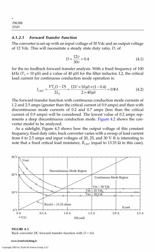
64
Practical Computer Analysis of Switch Mode Power Supplies
*.PROBE.END
4.1.2.1 Forward Transfer Function
The converter is set up with an input voltage of 30 Vdc and an output voltageof 12 Vdc. This will necessitate a steady state duty ratio,
D
, of
(4.1)
for the no feedback forward transfer analysis. With a fixed frequency of 100kHz (
T
S
= 10
µ
S) and a value of 40
µ
H for the filter inductor, L2, the criticalload current for continuous conduction mode operation is:
(4.2)
The forward transfer function with continuous conduction mode currents of1.2 and 2.5 amps (greater than the critical current of 0.9 amps) and then withdiscontinuous mode currents of 0.2 and 0.7 amps (less than the criticalcurrent of 0.9 amps) will be considered. The lowest value of 0.2 amps rep-resents a deep discontinuous conduction mode. Figure 4.2 shows the con-verter model to be analyzed.
As a sidelight, Figure 4.3 shows how the output voltage of this constantfrequency, fixed duty ratio, buck converter varies with a sweep of load currentfrom 0 to 2.5 amps and input voltages of 20, 25, and 30 V. It is interesting tonote that a fixed critical load resistance,
R
CRIT
(equal to 13.33
Ω
in this case),
FIGURE 4.3
Buck converter DC forward transfer function with
D
= 0.4.
Dvv
= =1230
0 4.
IVT D
LV S
SCRITS=
−= × × −
×=
( ) ( . ).
12
12 10 1 0 42 40
02
µµ
99A
30 V
20 V
10 V
0 V0 A 0.5 A
R(crit) = 13.33 ohms
Vout
Vin = 30 Vdc
V(1)1.0 A
l(ILoad)
ILoad
1.5 A 2.0 A 2.5 A
Discontinuous Mode Region
Continuous Mode Region
Vin = 25 VdcVin = 20 Vdc
DK_1137.book Page 64 Wednesday, June 15, 2005 11:49 AM
Copyright 2005 by Taylor & Francis Group, LLC
www.IranSwitching.ir

Analyzing the Fundamental SMPS Model
65
exists as noted by the straight line intersection of all the critical conductionpoints separating continuous and discontinuous conduction modes.
Now consider the AC forward transfer characteristics. A constant inputvoltage of 30 Vdc,
D
= 0.4, and the same two pair of continuous and discon-tinuous mode DC load current are used here also. For this example, thecorner frequencies of the input and output filter are purposefully separatedfrom each other in order to show their possible individual effects. Figure 4.4shows the transfer function for just the converter portion (node 8 to node 1in the simulation), and Figure 4.5 shows the overall transfer function, includ-ing the input filter. Notice that both continuous mode current transfer
FIGURE 4.4
Buck converter AC forward transfer function.
FIGURE 4.5
Buck converter AC forward transfer function with input filter added.
20
0
1.0 Hz 10 HzDB(V(1)) − DB(V(B))
100 HzFrequency
1.0 KHz 10 KHz 100 KHz
−20
−40
−60
−80
−100
ContinuousModes
Discontinuous Mode
Vin = 30 Vdc
20
0
−20
1.0 Hz 10 Hz
Discontinuous Modes
Continuous Modes Vin = 30 Vdc
DB(V(1))100 Hz
Frequency1.0 KHz 10 KHz 100 KHz
−40
−60
−80
−100
DK_1137.book Page 65 Wednesday, June 15, 2005 11:49 AM
Copyright 2005 by Taylor & Francis Group, LLC
www.IranSwitching.ir

66
Practical Computer Analysis of Switch Mode Power Supplies
functions are the same and are independent of load current, but the discon-tinuous mode transfer function varies with load. The smaller the load is, thelower the initial low frequency break point is.
Another interesting observation for the discontinuous mode case is that theconverter attenuation starts to flatten out after the output filter capacitor, C3,breaks with it series resistance, R3, at a frequency of 400 Hz. For the continuousmode case with the output filter (L2, C3) near critical damping, an attenuationslope of only 20 dB/Dec occurs after its corner frequency of approximately600 Hz. Figure 4.5 shows the transfer functions with the addition of the inputfilter section. For the continuous mode currents, the additional attenuationand steeper slope occur after the input filter corner frequency (approximately5 kHz). The two discontinuous mode current cases also show the additionalattenuation provided by the input filter addition.
4.1.2.2 Output Impedance (Voltage Mode)
Now look at the AC output impedance of the converter for the same condi-tions as those set up in the previous paragraph. (The input filter sectionremains in the circuit unless otherwise noted.) Figure 4.6 shows the ACoutput impedance plots. (0 dB is equivalent to 1
Ω
.) The discontinuous modeoutput impedance is relatively high and also a function of the load currentprior to breaking with the output filter capacitor, C3, at frequencies near 10Hz. At the low frequencies, the output impedance for the continuous mode isessentially the inductive reactance of inductor L2 in series with the reactanceof L2 reflected by the duty ratio squared (
D
2
).
4.1.2.3 Control to Output (Voltage Mode)
Examine the DC transfer functions for the control,
D
, to output voltage,
v
.The input voltage will be maintained constant at 30.0 Vdc; in this case, the
FIGURE 4.6
Buck converter output impedance (voltage mode).
40
20
0
−20
−40
−60
−801.0 Hz 10 Hz
Discontinuous Modes
Continuous Modes
Vin = 30 Vdc
DB(V(1))100 Hz
Frequency1.0 KHz 10 KHz 100 KHz
DK_1137.book Page 66 Wednesday, June 15, 2005 11:49 AM
Copyright 2005 by Taylor & Francis Group, LLC
www.IranSwitching.ir

Analyzing the Fundamental SMPS Model
67
duty ratio,
D
, will be varied over its range of 0 to 1. Figure 4.7 shows theDC transfer functions for values of
D
stepped from 0 to 1 in increments of0.1. Load currents were swept from 0 to 2.5 amps as was the case for theforward transfer function analysis. Note that the output voltage is indepen-dent of load current for continuous mode conduction and varying with loadcurrent for discontinuous modes. Of course, the duty ratio must vary con-siderably with load current in the discontinuous mode to regulate the outputvoltage, but theoretically may remain fixed for continuous mode currents.It is interesting to note the parabolic loci generated by connecting the criticalcurrent points for each of the stepped values of
D
. Also, note the maximumcritical current occurring at the duty ratio of
D
= 0.5. Now consider the AC control to output transfer functions. The same two
pairs of continuous and discontinuous mode DC load currents will be usedas were used for the forward voltage transfer analysis when analyzing theAC forward transfer function (continuous conduction mode currents of 1.2and 2.5 amps and discontinuous mode currents of 0.2 and 0.7 amps). Also,as was the case for the forward transfer function, the input will be set to aconstant 30 Vdc and the control,
D
, to a DC biased value of 0.4 while this ismodulated with the small signal AC stimulus.
Figure 4.8 shows the results. Note that the discontinuous mode gainsrolling off at lower corner frequencies are very much proportional to loadcurrent. The continuous mode gains roll off at higher frequencies and areseen to be fairly independent of load current. A very small, almost imper-ceptible dip in gain is noted around 2 kHz. This secondary effect is producedby the finite output impedance of the input filter. When analyzed with theinput filter removed (not shown here), this small dip disappears. On theother hand, with an improperly designed input filter, this gain dip mayincrease and cause such negative effects as reduced loop gain; reduced
FIGURE 4.7
Buck converter DC “control to output” transfer function with
Vin
= 30 Vdc (voltage mode).
30 V
20 V
10 V
0 V0 A 0.5 A
Continuous Mode
Discontinuous Mode
D = 0.2
D = 0.4D = 0.5
D = 0.6
D = 0.8
D = 1.0
V(1)1.0 A
ILoad1.5 A 2.0 A 2.5 A
DK_1137.book Page 67 Wednesday, June 15, 2005 11:49 AM
Copyright 2005 by Taylor & Francis Group, LLC
www.IranSwitching.ir

68
Practical Computer Analysis of Switch Mode Power Supplies
forward transfer attenuation; and higher output impedance; in severe cases,an input filter oscillating instability may occur.
2,13
4.1.3 SMPS Closed Loop Analysis (Continuous and Discontinuous Modes)
Now add the feedback control circuit, which regulates the output voltage to12 Vdc, and consider the SMPS characteristics and performance with thisaddition. Figure 4.9a shows the basic configuration. (A PSPICE netlist,labeled Netlist 4.2, is used for these voltage mode closed loop analysissimulations.) Using the same buck converter, an error amplifier has beenadded, along with a 2.5-V reference. Then the PWM gain block is insertedand combined with the AC-only loop opening, ultralow-pass filter circuit.It comprises LOL, COL, and VAC. This allows one to maintain the normalclosed loop DC operating points while examining the small signal AC openloop characteristics at these operating points. This technique will be usedrepeatedly in many of the future analyses. VAC is the signal injection stim-ulus necessary for any AC gain measurement or analysis. The PWM gain is:
(4.3)
where
V
M
is the PWM ramp amplitude (
V
M
= 1 V for these simulations). Theinput voltage and load currents are then varied over the same ranges as wasdone for the preceding open loop analysis. (Figure 4.9b shows the extremelysimple op amp model used for illustration purposes.)
FIGURE 4.8
Buck converter AC “
d
to output” transfer function (voltage mode).
40
20
0
1.0 Hz 10 HzDB (V(1))
100 Hz 1.0 KHzFrequency
Discontinuous Modes
Continuous Modes
Vin = 30 Vdc
10 KHz 100 KHz−20
dV
VM
= ( )13
DK_1137.book Page 68 Wednesday, June 15, 2005 11:49 AM
Copyright 2005 by Taylor & Francis Group, LLC
www.IranSwitching.ir

Analyzing the Fundam
ental SMP
S Model
69
FIGURE 4.9a
Buck converter switching regulator (voltage mode).
V FER
.2 5 V
-
+
d
CAV1
LOC
LOL
DER1
DG1
D
2D
1D
31
21
01
11+
rrE o A r mpPu esl iW htd
rotaludoM
A“ L C o po epO ren ”artlU( saP woL s retliF )
4R83 K
5R01 K
1XSAO IMP
6R03 K
5C0.0 1 Fu
6C074 Fp
2LHµ 04
3Cµ 0002 F 4C
.0 µ 1 F
3R2.0 Ω
I OL DA
2.0 - 2.5 A
+
V NI
81 03- V
1Lµ 05 H
1CFµ 571
2CFµ 01
1R.1 0 Ω
+
d
d
+
+
+N
9
8
7
65
2
41
3
Vg V
K
1DX
2DX
DX 3
i( DLI )
i( DL )
1E
MV 1V 0
MV 3V 0
d
MV 2V 1
1G
2F1
Po ew C r evno r retDLG
DLIG
+
DK
_1137.book Page 69 Wednesday, June 15, 2005 11:49 A
M
Copyright 2005 by T
aylor & Francis G
roup, LL
C
www.IranSwitching.ir

70
Practical Computer Analysis of Switch Mode Power Supplies
NETLIST 4.2
BUCK CONVERTER SMPS, VOLTAGE MODE, CLOSED LOOP ANALYSIS******************************************************************* SOURCE-LOAD CONFIGURATION FOR** FIGURES 4.10 AND 4.11** BUCK SMPS AC LOOP GAIN AND PHASE** WITH LOAD CHANGE (VOLTAGE MODE)*VIN N 0 DC 30 AC 0ILOAD 1 0 DC .2.STEP ILOAD LIST .2 .7 1.2 2.5LOL D1 D 1KCOL D D2 1KVAC 0 D2 AC 1.AC DEC 20 1 100K******************************************************************* SOURCE-LOAD CONFIGURATION FOR** FIGURES 4.12 AND 4.13** BUCK SMPS AC LOOP GAIN AND PHASE** WITH INPUT VOLTAGE CHANGE (VOLTAGE MODE)**ILOAD 1 0 DC 2.5*ILOAD 1 0 DC .2*VIN N 0 DC 18*.STEP VIN LIST 18 30*LOL D1 D 1K
FIGURE 4.9b
Simple 1.0-MHz bandwidth op amp model.
RIN10 MEG
G1100K
RO10
C00.016
+
-
OUTINPUT
31
2
DK_1137.book Page 70 Wednesday, June 15, 2005 11:49 AM
Copyright 2005 by Taylor & Francis Group, LLC
www.IranSwitching.ir

Analyzing the Fundamental SMPS Model
71
*COL D D2 1K*VAC 0 D2 AC 1*.AC DEC 20 1 100K******************************************************************* SOURCE-LOAD CONFIGURATION FOR** FIGURES 4.14 AND 4.15** BUCK SMPS AC OUTPUT IMPEDANCE** WITH INPUT VOLTAGE CHANGE (VOLTAGE MODE)**ILOAD 1 0 DC 2.5*ILOAD 1 0 DC .2*VIN N 0 DC 18*.STEP VIN LIST 18 30*LOL D1 D 1P*COL D D2 1P*VAC 0 D2 AC 0*IAC 1 0 AC 1*.AC DEC 20 1 100K******************************************************************* SOURCE-LOAD CONFIGURATION FOR** FIGURES 4.16 AND 4.17** BUCK SMPS AC FORWARD ATTENUATION ** WITH INPUT DC VOLTAGE CHANGE (VOLTAGE MODE)**ILOAD 1 0 DC .2*ILOAD 1 0 DC 2.5*VIN N 0 DC 30 AC 1*.STEP VIN LIST 18 30*LOL D1 D 1P*COL D D2 1P*VAC 0 D2 AC 0*.AC DEC 20 1 100K*.NODESET V(1)=12 V(8)=30 V(13)=1******************************************************************* SOURCE-LOAD CONFIGURATION FOR** FIGURES 4.19 AND 4.20** BUCK SMPS AC FORWARD ATTENUATION WITH FEEDFORWARD COMPENSATION** WITH INPUT DC VOLTAGE CHANGE (VOLTAGE MODE)**ILOAD 1 0 DC .2*ILOAD 1 0 DC 2.5*VIN N 0 DC 30 AC 1*.STEP VIN LIST 18 30*LOL D1 D 1P*COL D D2 1P*VAC 0 D2 AC 0*.AC DEC 20 1 100K*.NODESET V(1)=12 V(8)=30 V(13)=1
DK_1137.book Page 71 Wednesday, June 15, 2005 11:49 AM
Copyright 2005 by Taylor & Francis Group, LLC
www.IranSwitching.ir

72
Practical Computer Analysis of Switch Mode Power Supplies
*.OPTIONS GMIN=1E-10*** NOTE: THE FOLLOWING GD REMAINS IN THE CIRCUIT FOR ALL OTHER ANALYSIS** BUT MUST ALTERNATE WITH THE SECOND GD BELOW FOR THIS ** BUCK SMPS AC FEEDFORWARD ATTENUATION ANALYSIS ONLYGD 0 D1 13 0 1*GD 0 D1 VALUE = LIMIT((12*V(13))/V(8),0,1)*******************************************************************VOLTAGE MODE SMPS NETLIST*RED D1 0 1C4 1 0 .1UC3 1 3 2000UR3 3 0 .2GLD 2 K VALUE = V(D)**2*(V(8)/V(1))*(V(8)-V(1))*.125VM3 K 1XD3 2 1 DIDEALL2 4 2 40UE1 4 5 VALUE = V(8)*V(D)VM1 0 5GILD 6 7 VALUE = I(VM3)*V(1)/V(8)G1 0 6 VALUE = I(VM1)*V(D)XD1 6 7 DIDEALXD2 0 6 DIDEALVM2 7 0 DC 1F2 8 0 VM2 1C2 8 0 10UC1 8 9 175UR1 9 0 1L1 N 8 50UR4 1 10 38KR5 10 0 10KVREF 11 0 DC 2.5X1 11 10 13 OASIMPC5 13 12 .01UR6 12 10 30KC6 12 10 470P*.SUBCKT OASIMP 1 2 3RIN 1 2 10MEGG1 0 3 1 2 100KRO 3 0 10CO 3 0 .016.ENDS OASIMP*.SUBCKT DIDEAL 1 2VAS 1 3 DC -1UD1 3 2 DD2 3 4 DD3 4 2 D1FAS 4 2 VAS 1.MODEL D D IS=1E-6.MODEL D1 D
DK_1137.book Page 72 Wednesday, June 15, 2005 11:49 AM
Copyright 2005 by Taylor & Francis Group, LLC
www.IranSwitching.ir

Analyzing the Fundamental SMPS Model
73
CC 1 2 .1P.ENDS DIDEAL*.PROBE
.END
4.1.3.1 AC Loop Gain (Voltage Mode)
Figure 4.10 shows the AC loop gain and phase plots for the two continuousmode loads of 1.2 and 2.5 amps, and Figure 4.11 shows the AC loop gain andphase plots for the two discontinuous mode loads of 0.2 and 0.7 amps. Thecontinuous mode gains in Figure 4.10 are independent of load current varia-tions, as might be expected; however, the gains in the discontinuous modecases of Figure 4.11 do vary with load current, as also might be expected. Notethat the unity gain crossover frequency is reduced for the discontinuous modecases and continues to decrease for further decreasing loads.
To ensure that the feedback control loop maintains AC stability, the phaseshift must not approach or exceed a magnitude of –180
°
at the unity gaincrossover frequency. The actual phase difference, or “phase margin,” from–180
°
at the unity gain crossover frequency is conventionally considered themost important figure of merit for determining the degree of AC stability ofa feedback control system. The accompanying figure of merit is the gainmargin. This is the reduction in loop gain magnitude below unity (0 dB)corresponding to the –180
°
phase shift point. Typical numbers desired for thephase and gain margin are 45
°
and 10 dB. See Kuo
10
and D’Azzo and Houpis
11
for more fundamental information on feedback control stability.Now consider the effects of input DC voltage variations on loop gain by
stepping
V
in
from 18 to 30 Vdc with the load cases of 2.5 amps (continuous)
FIGURE 4.10
Buck SMPS continuous mode AC loop gain and phase with load change (voltage mode).
0 d
P(V(D1))
Loop Phase
Loop Gain Vin = 30 Vdc
DB(V(D1))
−50 d
−100 d
−150 d
−200 d
−40
10080604020
0
1.0 Hz 10 Hz 100 HzFrequency
1.0 KHz 10 KHz 100 KHz
SEL>
>
DK_1137.book Page 73 Wednesday, June 15, 2005 11:49 AM
Copyright 2005 by Taylor & Francis Group, LLC
www.IranSwitching.ir

74
Practical Computer Analysis of Switch Mode Power Supplies
and 0.2 amps (discontinuous). Figure 4.12 and Figure 4.13 show the respec-tive plots. Both plots indicate a shift in gain that is somewhat proportionalto the input voltage change ratio.
4.1.3.2 SMPS Output Impedance (Voltage Mode)
Now look at the SMPS output impedance for extreme variations in line voltageand load currents that were considered in the preceding loop gain analyses.By examining the plots of Figure 4.14 and Figure 4.15, AC impedance
FIGURE 4.11
Buck SMPS discontinuous mode AC loop gain and phase with load change (voltage mode).
FIGURE 4.12
Buck SMPS continuous mode AC loop gain and phase with input voltage change (voltage mode).
0 d
P(V(D1))
Loop Phase
Loop Gain
Load = 0.2 Adc
Load = 0.7 Adc
Vin = 30 Vdc
DB(V(D1))
−50 d
−100 d
−150 d
−200 d
−40
10080604020
0
1.0 Hz 10 Hz 100 HzFrequency
1.0 KHz 10 KHz 100 KHz
SEL>
>
0 d
P(V(D1))
Loop Phase
Loop GainLoad = 2.5 Amps
(ContinuousMode)Vin = 18 Vdc
Vin = 30 Vdc
DB(V(D1))
−50 d
−100 d
−150 d
−200 d
−40
10080604020
0
1.0 Hz 10 Hz 100 HzFrequency
1.0 KHz 10 KHz 100 KHz
SEL>
>
DK_1137.book Page 74 Wednesday, June 15, 2005 11:49 AM
Copyright 2005 by Taylor & Francis Group, LLC
www.IranSwitching.ir

Analyzing the Fundamental SMPS Model
75
magnitudes for input voltages of 18 and 30 Vdc, respectively, can be observed.The 30-Vdc cases provide higher loop gains, which produce the lower outputimpedances that might be expected (see Equation 2.2). To illustrate specificallyfor the 30-Vdc input case, the impedance plots of Figure 4.14 and Figure 4.15could be essentially derived by dividing the open loop impedance of Figure4.6 by one plus the corresponding loop gains of Figure 4.12 and Figure 4.13(see Equation 2.2).
FIGURE 4.13
Buck SMPS discontinuous mode AC loop gain and phase with input voltage change (voltagemode).
FIGURE 4.14
Buck SMPS continuous mode AC output impedance with input voltage change.
0 d
P(V(D1))
Loop Phase
Loop GainLoad = 0.2 Amps(Discontinuous
Mode)Vin = 18 Vdc
Vin = 30 Vdc
DB(V(D1))
−50 d
−100 d
−150 d
−200 d
−40−20
10080604020
0
1.0 Hz 10 Hz 100 HzFrequency
1.0 KHz 10 KHz 100 KHz
SEL>
>
ZoutLoad = 2.5 Amps
(Continuous Mode)
Vin = 18 Vdc
Vin = 30 Vdc
DB(V(1))
−160
−140
−120
−100
−80
−60
−40
−20
0
1.0 Hz 10 Hz 100 HzFrequency
1.0 KHz 10 KHz 100 KHz
DK_1137.book Page 75 Wednesday, June 15, 2005 11:49 AM
Copyright 2005 by Taylor & Francis Group, LLC
www.IranSwitching.ir
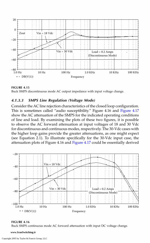
76
Practical Computer Analysis of Switch Mode Power Supplies
4.1.3.3 SMPS Line Regulation (Voltage Mode)
Consider the AC line rejection characteristics of the closed loop configuration.This is sometimes called “audio susceptibility.” Figure 4.16 and Figure 4.17show the AC attenuation of the SMPS for the indicated operating conditionsof line and load. By examining the plots of these two figures, it is possibleto observe the AC forward attenuation at input voltages of 18 and 30 Vdcfor discontinuous and continuous modes, respectively. The 30-Vdc cases withthe higher loop gains provide the greater attenuations, as one might expect(see Equation 2.1). To illustrate specifically for the 30-Vdc input case, theattenuation plots of Figure 4.16 and Figure 4.17 could be essentially derived
FIGURE 4.15
Buck SMPS discontinuous mode AC output impedance with input voltage change.
FIGURE 4.16
Buck SMPS continuous mode AC forward attenuation with input DC voltage change.
Zout
Load = 0.2 Amps(Discontinuous Mode)
Vin = 18 Vdc
Vin = 30 Vdc
DB(V(1))
−20
−40
−60
−80
0
20
1.0 Hz 10 Hz 100 HzFrequency
1.0 KHz 10 KHz 100 KHz
Load = 0.2 Amps(Discontinuous Mode)
Vin = 18 Vdc
Vin = 30 Vdc
DB(V(1))
−20
−40
−60
−80
−1001.0 Hz 10 Hz 100 Hz
Frequency1.0 KHz 10 KHz 100 KHz
DK_1137.book Page 76 Wednesday, June 15, 2005 11:49 AM
Copyright 2005 by Taylor & Francis Group, LLC
www.IranSwitching.ir

Analyzing the Fundamental SMPS Model
77
by dividing the open loop attenuations of Figure 4.8 by one plus the corre-sponding loop gains of Figure 4.12 and Figure 4.13 (Equation 2.1).
4.1.3.4 SMPS Feedforward Analysis
In many applications that utilize voltage mode control, the AC line rejectionrequirements are sometimes difficult to satisfy because of the difficulty inachieving the required AC loop gain and maintaining AC loop stability inthe continuous mode. One technique of improving this situation is to providea type of input voltage feedforward. This is implemented by letting the slopeof the pulse width modulator (PWM) control ramp (Figure 4.1) be propor-tional to the input line voltage. For fixed-frequency converters, this translatesinto a control ramp amplitude that is proportional to input voltage.
Since the PWM gain is inversely proportional to this ramp amplitude, it hasthe effect of
reducing
loop gain with increasing input voltage. On the otherhand, an increasing input voltage will increase the converter control to outputgain, thereby
increasing
loop gain. With these offsetting effects, the feedbackcontrol loop can effectively be fixed and “linearized” by being almost if notcompletely independent of input voltage variations. Although this gain stabi-lizing effect simplifies the control loop, the AC line rejection improvement isin reality achieved by the immediate duty ratio adjustment being made withthe immediate change in input voltage. Perfect feedforward compensation isgenerally not practical, but considerable improvements can be realized.
Take the open loop converter that produced the results of Figure 4.5 and,instead of a fixed
D
= 0.4, ideally add some feedforward by letting
d
havethe following inverse relationship to
V
g
:
(4.4)
FIGURE 4.17
Buck SMPS discontinuous mode AC forward attenuation with input DC voltage change.
Load = 2.5 Amps(Continuous
Mode)
Vin = 18 Vdc
Vin = 30 Vdc
DB(V(1))
−20
−40
−60
−80
−1001.0 Hz 10 Hz 100 Hz
Frequency1.0 KHz 10 KHz 100 KHz
dvvg
V
vgg
= ( ) = ( ) =1 1 12
12
DK_1137.book Page 77 Wednesday, June 15, 2005 11:49 AM
Copyright 2005 by Taylor & Francis Group, LLC
www.IranSwitching.ir

78
Practical Computer Analysis of Switch Mode Power Supplies
Comparing the results of Figure 4.5 to those in Figure 4.18 makes it possibleto see the dramatic increase in line to output attenuation for the continuousmode cases at the lower frequencies (
∼
60 dB improvement). The discontin-uous modes are only slightly affected.
4.1.4 SMPS Combined Feedback and FeedforwardAnalysis (Line Regulation)
Now take the closed loop feedback regulated circuit of Figure 4.9 and addthe feedforward implementation of Section 4.1.3.4 to it and compare the ACline rejection characteristics to those obtained with feedback only, as shownin Figure 4.16 and Figure 4.17. With the PWM control ramp amplitudesimply modulated by the input voltage, the implementation is simply tomultiply the circuit model control voltage,
d
, by a function inversely pro-portional to the input voltage. A function as expressed by Equation 4.5might be a possible idealistic implementation:
(4.5)
The results are shown in Figure 4.19 and Figure 4.20. Compare thesefigures with Figure 4.16 and Figure 4.17, respectively, and note theimprovement in forward attenuation with the addition of the feedforwardcompensation. About 50 dB of additional attenuation was noted for the
FIGURE 4.18
Buck converter AC forward transfer function with feedforward.
DB(V(1))
−20
−40
−60
−80
−100
−120
−140
−160
0
1.0 Hz 10 Hz
Continuous Modes
Discontinuous Modes Vin = 30 Vdc
100 HzFrequency
1.0 KHz 10 KHz 100 KHz
dv v
ve
vg
e
g
= ( ) =⎛
⎝⎜⎜
⎞
⎠⎟⎟
12
12
DK_1137.book Page 78 Wednesday, June 15, 2005 11:49 AM
Copyright 2005 by Taylor & Francis Group, LLC
www.IranSwitching.ir

Analyzing the Fundamental SMPS Model
79
continuous mode cases, but practically no noticeable increase was notedfor the discontinuous mode cases. The idealistic feedforward additionconsidered here, combined with the feedback, provides somewhat ide-alistic results that may not be achievable in actual practice. Neverthe-less, the method of analysis and the general expected results have beenshown.
FIGURE 4.19
Buck SMPS with feedforward compensation. Continuous mode AC forward attenuation withinput DC voltage change.
FIGURE 4.20
Buck SMPS with feedforward compensation. Discontinuous mode AC forward attenuation withinput DC voltage change.
DB(V(1))
−60
−80
−140
−120
−100
1.0 Hz 10 Hz
Load = 2.5 Amps(Continuous Mode)
Vin = 30 Vdc
Vin = 18 Vdc
100 HzFrequency
1.0 KHz 10 KHz 100 KHz
DB(V(1))
−20
−40
−100
−80
−60
1.0 Hz 10 Hz
Load = 0.2 Amps(Discontinuous Mode)
Vin = 30 Vdc
Vin = 18 Vdc
100 HzFrequency
1.0 KHz 10 KHz 100 KHz
DK_1137.book Page 79 Wednesday, June 15, 2005 11:49 AM
Copyright 2005 by Taylor & Francis Group, LLC
www.IranSwitching.ir

80
Practical Computer Analysis of Switch Mode Power Supplies
4.2 Buck Converter SMPS Analysis (Current Mode)
A current mode control converter actually starts out as the voltage modeconverter described in Section 4.1. An inductor current sense circuit is addedand a feedback control loop is established so that an applied control signalcan regulate or control the inductor current. Several types of control for thiscurrent are possible, depending on the desired characteristics. When theinductor current is triangular and has an averaged DC value, one can senseand regulate the peak current or, in some cases, the converse valley current.In some designs, the average inductor current is determined and regulated,providing a possibly more desirable control for some applications. For out-put voltage regulation, a second outer control loop circuit senses outputvoltage and its output provides the control signal for regulating the inductorcurrent. Controlling the inductor current subsequently allows regulation ofthe output voltage.
5,12
(A PSPICE netlist, labeled Netlist 4.3, is used for thesecurrent mode analysis simulations.)
NETLIST 4.3
BUCK CONVERTER SMPS, CURRENT MODE, ANALYSIS******************************************************************* SOURCE-LOAD CONFIGURATION FOR** FIGURES 4.24 AND 4.25** BUCK SMPS AC LOOP GAIN AND PHASE** WITH LOAD CHANGE (CURRENT MODE)*VIN N 0 DC 30ILOAD 1 0 DC .2.STEP ILOAD LIST .2 .7 1.2 2.5LOL 14 16 1KCOL 16 15 1KVAC 0 15 AC 1.AC DEC 20 1 100K.OPTIONS ITL2=200******************************************************************* SOURCE-LOAD CONFIGURATION FOR** FIGURES 4.26 AND 4.27** BUCK SMPS AC LOOP GAIN AND PHASE** WITH INPUT VOLTAGE CHANGE (CURRENT MODE)**ILOAD 1 0 DC 2.5*ILOAD 1 0 DC .2*VIN N 0 DC 30*.STEP VIN LIST 18 30*LOL 14 16 1K*COL 16 15 1K*VAC 0 15 AC 1*.AC DEC 20 1 100K
DK_1137.book Page 80 Wednesday, June 15, 2005 11:49 AM
Copyright 2005 by Taylor & Francis Group, LLC
www.IranSwitching.ir

Analyzing the Fundamental SMPS Model
81
*.OPTIONS STEPGMIN ITL2=200*.NODESET V(1)=12 V(8)=30 V(D)=.6 V(17)=1 V(13)=1 V(14)=1******************************************************************* SOURCE-LOAD CONFIGURATION FOR** FIGURE 4.28** OUTPUT IMPEDANCE OF THE “OPEN VOLTAGE LOOP” CURRENT MODE** CONVERTER**ILOAD 1 0 DC .2*.STEP ILOAD LIST .2 .7 1.2 2.5*VIN N 0 DC 30*LOL 14 16 1K*COL 16 15 1K*VAC 0 15 AC 0*IAC 1 0 AC 1*.AC DEC 20 1 100K*.OPTIONS STEPGMIN ITL2=200******************************************************************* SOURCE-LOAD CONFIGURATION FOR** FIGURE 4.29 AND 4.30** AC FORWARD TRANSFER FUNCTION OF THE “OPEN VOLTAGE LOOP” ** CURRENT MODE CONVERTER WITHOUT THE INPUT FILTER.* *ILOAD 1 0 DC .2*.STEP ILOAD LIST .2 .7 1.2 2.5*VIN N 0 DC 30 AC 1 *LOL 14 16 1K*COL 16 15 1K*VAC 0 15 AC 0*.AC DEC 20 1 100K*.OPTIONS STEPGMIN ITL2=200******************************************************************* SOURCE-LOAD CONFIGURATION FOR** FIGURE 4.31**BUCK CONVERTER AC “D TO OUTPUT” TRANSFER FUNCTION (CURRENT MODE).**ILOAD 1 0 DC .2*.STEP ILOAD LIST .2 .7 1.2 2.5*VIN N 0 DC 30 *LOL 14 16 1K*COL 16 15 1K*VAC 0 15 AC 1*.AC DEC 20 1 100K*.OPTIONS STEPGMIN ITL2=200******************************************************************* SOURCE-LOAD CONFIGURATION FOR** FIGURE 4.32** INNER INDUCTOR CURRENT CONTROL LOOP GAIN**ILOAD 1 0 DC .2*.STEP ILOAD LIST 1.2 2.5
DK_1137.book Page 81 Wednesday, June 15, 2005 11:49 AM
Copyright 2005 by Taylor & Francis Group, LLC
www.IranSwitching.ir

82 Practical Computer Analysis of Switch Mode Power Supplies
*VIN N 0 DC 30 *LOL 14 16 1K*COL 16 15 1K*VAC 0 15 AC 0*HI 100 0 VM1 1*LOL2 100 101 1000*COL2 101 102 1000*VAC2 0 102 AC 1*.AC DEC 20 1 100K*.OPTIONS STEPGMIN ITL2=200*** NOTE: THE FOLLOWING EDC REMAINS IN THE CIRCUIT FOR ALL ANALYSIS** BUT MUST ALTERNATE WITH THE SECOND EDC BELOW FOR THIS ** INNER INDUCTOR CURRENT CONTROL LOOP GAIN ANALYSIS ONLYEDC 17 0 VALUE = (V(16)/1-I(VM1))/(.125*(24+V(8)-V(1)))*EDC 17 0 VALUE = (V(16)/1-V(101))/(.125*(24+V(8)-V(1)))******************************************************************* SOURCE-LOAD CONFIGURATION FOR** FIGURE 4.33** OUTPUT IMPEDANCE OF THE CURRENT MODE SMPS**ILOAD 1 0 DC .2*.STEP ILOAD LIST .2 .7 1.2 2.5*VIN N 0 DC 30 *LOL 14 16 1P*COL 16 15 1P*VAC 0 15 AC 0*IAC 1 0 AC 1*.AC DEC 20 1 100K*.OPTIONS STEPGMIN ITL2=200******************************************************************* SOURCE-LOAD CONFIGURATION FOR** FIGURE 4.34 AND 4.35** AC LINE REJECTION OF THE CURRENT MODE SMPS**VIN N 0 DC 30 AC 1*VIN N 0 DC 18 AC 1*ILOAD 1 0 DC .2*.STEP ILOAD LIST .2 .7 1.2 2.5*LOL 14 16 1P*COL 16 15 1P*VAC 0 15 AC 0*.AC DEC 20 1 100K*.OPTIONS STEPGMIN ITL2=200*.NODESET V(1)=12 V(8)=30 V(D)=.6 V(17)=1 V(13)=1 V(14)=1*******************************************************************CURRENT MODE SMPS NETLIST*C4 1 0 .1U
DK_1137.book Page 82 Wednesday, June 15, 2005 11:49 AM
Copyright 2005 by Taylor & Francis Group, LLC
www.IranSwitching.ir

Analyzing the Fundamental SMPS Model 83
C3 1 3 2000UR3 3 0 .2GLD 2 K VALUE = V(D)**2*(V(8)/V(1))*(V(8)-V(1))*.125VM3 K 1XD3 2 1 DIDEALL2 4 2 40UE1 4 5 VALUE = V(8)*V(D)VM1 0 5GILD 6 7 VALUE = I(VM3)*V(1)/V(8)G1 0 6 VALUE = I(VM1)*V(D)XD1 6 7 DIDEALXD2 0 6 DIDEALVM2 7 0 DC 1F2 8 0 VM2 1C2 8 0 10UC1 8 9 175UR1 9 0 1L1 N 8 50UR4 1 10 38KR5 10 0 10KVREF 11 0 DC 2.5X1 11 10 13 OASIMPC5 13 12 .01UR6 12 10 300KC6 12 10 470PEVC 14 0 13 0 1*.SUBCKT OASIMP 1 2 3RIN 1 2 10MEGG1 0 3 1 2 100KRO 3 0 10CO 3 0 .016.ENDS OASIMP*X2 D 17 DIDEALEDD 18 0 VALUE = (V(16)/1)/(.25*(12+V(8)-V(1)))X3 D 18 DIDEALIRM 0 D DC 1MRM 0 D 10K*.SUBCKT DIDEAL 1 2VAS 1 3 DC -1UD1 3 2 DD2 3 4 DD3 4 2 D1FAS 4 2 VAS 1.MODEL D D IS=1E-6.MODEL D1 DCC 1 2 .1P.ENDS DIDEAL*.PROBE.END
DK_1137.book Page 83 Wednesday, June 15, 2005 11:49 AM
Copyright 2005 by Taylor & Francis Group, LLC
www.IranSwitching.ir

84 Practical Computer Analysis of Switch Mode Power Supplies
4.2.1 Current Mode Converter Model Setup
To maintain a sense of consistency, use the same converter of Figure 4.1 andits model (Figure 4.2) and implement a current mode control scheme withit for the current mode analysis. Figure 4.21 and Figure 4.22 show the fun-damental inductor current and current control waveforms for the continuousand discontinuous modes of operation, respectively. From these waveforms,the following expressions for the control parameter, d, are determined. Slopem1 is the ON time slope of the inductor current and –m2 is the OFF timeslope. Slope mC is that of the stabilizing ramp added to the peak currentcontrol voltage, vC/Rf, for stability.12 For continuous conduction mode, d isderived from Figure 4.21 as:
(4.6)
FIGURE 4.21Peak current sensing current mode control waveforms (continuous conduction mode).
FIGURE 4.22Peak current sensing current mode control waveforms (discontinuous conduction mode).
iL(AVG)
⎟⎟⎠
⎞⎜⎜⎝
⎛
F
C
R
v
dTS
TS
d'TS
-mC
-m2m1
di
m L v v
vCR f L
TSL C g
=−
+ −
2
2 2 22( )
iL(AVG)
⎟⎟⎠
⎞⎜⎜⎝
⎛
F
C
Rv
dTS
TS
d2TS
-mC
-m2m1
0
DK_1137.book Page 84 Wednesday, June 15, 2005 11:49 AM
Copyright 2005 by Taylor & Francis Group, LLC
www.IranSwitching.ir

Analyzing the Fundam
ental SMP
S Model
85
FIGURE 4.23Buck converter switching regulator model (current mode).
V FER
.2 V 5
-
+VE C1
31
21
01
11+
E rorr pmA
4RK83
5RK01
1XSAO IMP
6R03 K0
5C0. u10 f
6C074 Fp
2LHµ 04
3Cµ 0002 F 4C
.0 Fµ 1
3R2.0 Ω
I OL DA
+
V NI
-81 dV 03 caV 0.1 c
1LHµ 05
1CFµ 571
2CFµ 01
1R.1 0 Ω
+
d
d
+
+
+N
9
8
7
65
2
41
3
Vg V
K
1DX
2DX
DX 3
i( DLI )
i( DL )
1E
MV 1V 0
MV 3V 0
d
MV 2V 1
1G
2F1
Po ew C r evno r ret
i 2L
vC
LOC
LOL
51
41
“AC ooL O p enep ”r(U rtl a oL ssaP w tliF )re
+
"d“
D
luP s tdiW e hludoM rota
++
7181
MRK1 CDEDDE
3XAEDID L
2XEDID LA
v(f C v , g )v , v(f C v , g, i ,v 2L )
61
+ AV C v C
LG D
DLIG
DK
_1137.book Page 85 Wednesday, June 15, 2005 11:49 A
M
Copyright 2005 by T
aylor & Francis G
roup, LL
C
www.IranSwitching.ir

86 Practical Computer Analysis of Switch Mode Power Supplies
and the discontinuous mode case from Figure 4.22 is:
(4.7)
The current mode analysis model is shown in Figure 4.23. The dependentvoltage source EDC will produce a voltage at node 17 that is equal to thecalculated magnitude of the continuous mode duty ratio, d, as expressed byEquation 4.6. The dependent voltage source EDD produces a voltage at node18 representing the calculated magnitude of the discontinuous mode dutyratio, d, expressed by Equation 4.7. Each of these two duty ratio parametersis continuously calculated and diode ORed by the two ideal diodes, X2 andX3, producing the smaller value of d at node D. This smaller value is thecorrect d to be used for control of the converter and will correspond to itscorrect conduction mode. (This is also true for the current mode boost andbuck–boost current mode topologies.) The correct conduction mode for theconverter is determined implicitly as usual. For optimum stability,5 mC is setequal to –m2 or
(4.8)
Rf will be 1 Ω because this scaling will be appropriate for this analysis(Chapter 6 contains more information about this selection). With the valueof TS still at 10 µS, and L2 at 40 µH, equations for the values of EDC andEDD can now be inserted in the model.
4.2.2 Open Voltage Loop AC Analysis (Continuous and Discontinuous Modes)
The plot of Figure 4.24 shows the continuous mode loop gain and phaseof the outer voltage control loop of the current mode switching regulator;Figure 4.25 shows the discontinuous mode cases. (The inner currentcontrol loop is closed via the equation for EDC.) The loads are the sameas they were for the voltage mode regulator in Section 4.1.3. The erroramplifier frequency response characteristic was modified from the volt-age mode example to provide more practical results for the current modeanalysis.
As was the case for the voltage mode converter, note that the continuousmode gains in Figure 4.24 are independent of load current variations (currentsink loads), but that the gains in the discontinuous mode case of Figure 4.25do vary with load currents. Note that the unity gain crossover frequency is
dm L v v
vCR f
C gTSL
=+ −
22( )
mVL
VH
VSC = = =
2
1240
0 3µ µ
.
DK_1137.book Page 86 Wednesday, June 15, 2005 11:49 AM
Copyright 2005 by Taylor & Francis Group, LLC
www.IranSwitching.ir

Analyzing the Fundamental SMPS Model 87
reduced for the discontinuous mode cases and continues to decrease forcontinuously decreasing loads. Also, to ensure that the feedback control loopmaintains AC stability, the phase shift must not approach or exceed a mag-nitude of –180° at the unity gain crossover frequency. As stated earlier, typicaldesired numbers for the phase and gain margins are 45° and 10 dB, respec-tively. Kuo10 and D’Azzo and Houpis11 offer more fundamental informationon feedback control stability.
Now consider the effects of input DC voltage variations on loop gain bystepping Vin from 18 to 30 Vdc with the load cases of 2.5 amps (continuous)
FIGURE 4.24Buck SMPS continuous mode AC loop gain and phase with load change (current mode).
FIGURE 4.25Buck SMPS discontinuous mode AC loop gain and phase with load change (current mode).
0 d
P(V(13))
Loop Phase
Loop Gain Vin = 30 Vdc
DB(V(13))
−75 d−50 d−25 d
−100 d
−150 d−125 d
−200 d
−20−40−60−80
80604020
0
1.0 Hz 10 Hz 100 HzFrequency
1.0 KHz 10 KHz 100 KHz
SEL>
>
0 d
P(V(13))
Loop Phase
Loop Gain Vin = 30 Vdc
DB(V(13))
−75 d−50 d−25 d
−100 d
−150 d−125 d
−200 d
−20−40−60−80
80604020
0
1.0 Hz 10 Hz 100 HzFrequency
1.0 KHz 10 KHz 100 KHz
SEL>
>
Load = 0.2 Adc
Load = 0.7 Adc
DK_1137.book Page 87 Wednesday, June 15, 2005 11:49 AM
Copyright 2005 by Taylor & Francis Group, LLC
www.IranSwitching.ir

88 Practical Computer Analysis of Switch Mode Power Supplies
and 0.2 amps (discontinuous). Figure 4.26 and Figure 4.27 show the respec-tive plots. Only the discontinuous mode case plot indicates a noticeable shiftin gain with the input voltage. This may not be true for all designs, but asmall change will generally be noticed.
4.2.2.1 Open Voltage Loop AC Output Impedance (Current Mode)
Now look at the AC output impedance of the converter for the same conditionsas those set up in the previous section. This is the output impedance of the
FIGURE 4.26Buck SMPS continuous mode AC loop gain and phase with input voltage change (current mode).
FIGURE 4.27Buck SMPS discontinuous mode AC loop gain and phase with input voltage change (currentmode).
0 d
P(V(13))
Loop Phase
Loop GainVin = 30 Vdc
Vin = 18.0 Vdc
DB(V(13))
−75 d−50 d−25 d
−100 d
−150 d−175 d
−125 d
−200 d
−20−40
−80
80604020
0
1.0 Hz 10 Hz
Load = 2.5 Amps(Continuous Mode)
100 HzFrequency
1.0 KHz 10 KHz 100 KHz
SEL>
>
0 d
P(V(13))
Loop Phase
Loop Gain Vin = 30 Vdc
Vin = 18.0 Vdc
DB(V(13))
−75 d−50 d−25 d
−100 d
−150 d−175 d
−125 d
−200 d
−20−40
−80
80604020
0
1.0 Hz 10 Hz
Load = 0.2 Amp(Discontinuous Mode)
100 HzFrequency
1.0 KHz 10 KHz 100 KHz
SEL>
>
DK_1137.book Page 88 Wednesday, June 15, 2005 11:49 AM
Copyright 2005 by Taylor & Francis Group, LLC
www.IranSwitching.ir
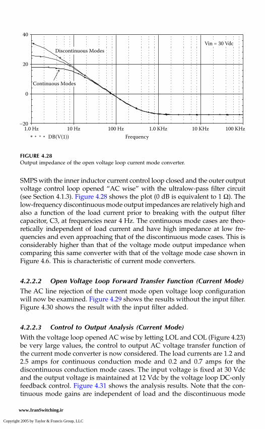
Analyzing the Fundamental SMPS Model 89
SMPS with the inner inductor current control loop closed and the outer outputvoltage control loop opened “AC wise” with the ultralow-pass filter circuit(see Section 4.1.3). Figure 4.28 shows the plot (0 dB is equivalent to 1 Ω). Thelow-frequency discontinuous mode output impedances are relatively high andalso a function of the load current prior to breaking with the output filtercapacitor, C3, at frequencies near 4 Hz. The continuous mode cases are theo-retically independent of load current and have high impedance at low fre-quencies and even approaching that of the discontinuous mode cases. This isconsiderably higher than that of the voltage mode output impedance whencomparing this same converter with that of the voltage mode case shown inFigure 4.6. This is characteristic of current mode converters.
4.2.2.2 Open Voltage Loop Forward Transfer Function (Current Mode)
The AC line rejection of the current mode open voltage loop configurationwill now be examined. Figure 4.29 shows the results without the input filter.Figure 4.30 shows the result with the input filter added.
4.2.2.3 Control to Output Analysis (Current Mode)
With the voltage loop opened AC wise by letting LOL and COL (Figure 4.23)be very large values, the control to output AC voltage transfer function ofthe current mode converter is now considered. The load currents are 1.2 and2.5 amps for continuous conduction mode and 0.2 and 0.7 amps for thediscontinuous conduction mode cases. The input voltage is fixed at 30 Vdcand the output voltage is maintained at 12 Vdc by the voltage loop DC-onlyfeedback control. Figure 4.31 shows the analysis results. Note that the con-tinuous mode gains are independent of load and the discontinuous mode
FIGURE 4.28Output impedance of the open voltage loop current mode converter.
1.0 Hz 10 Hz
40
20
0
−20100 Hz
FrequencyDB(V(1))
Continuous Modes
Discontinuous ModesVin = 30 Vdc
1.0 KHz 10 KHz 100 KHz
DK_1137.book Page 89 Wednesday, June 15, 2005 11:49 AM
Copyright 2005 by Taylor & Francis Group, LLC
www.IranSwitching.ir

90 Practical Computer Analysis of Switch Mode Power Supplies
cases do vary with load current. The gain decreases at a slope of –1, whichis generally characteristic of current mode converters in continuous anddiscontinuous modes of operation.
4.2.2.4 Inner Inductor Current Control Loop Gain
Occasionally, it may be desirable to examine the inner inductor current controlloop to see if its AC characteristics are as expected. This is accomplished byopening the inductor current feedback signal AC wise (this current is sensed
FIGURE 4.29AC forward transfer function of the open voltage loop current mode converter without theinput filter.
FIGURE 4.30AC forward transfer function of the open voltage loop current mode converter with input filteradded.
1.0 Hz 10 Hz
0
−120
−100
−80
−60
−40
−20
100 HzFrequencyDB(V(1)) − DB(V(B))
Discontinuous Modes
Continuous Modes Vin = 30 Vdc
1.0 KHz 10 KHz 100 KHz
1.0 Hz 10 Hz
0
−120
−100
−80
−60
−40
−20
100 HzFrequencyDB(V(1))
Discontinuous Modes
Continuous Modes Vin = 30 Vdc
1.0 KHz 10 KHz 100 KHz
DK_1137.book Page 90 Wednesday, June 15, 2005 11:49 AM
Copyright 2005 by Taylor & Francis Group, LLC
www.IranSwitching.ir

Analyzing the Fundamental SMPS Model 91
by VM1 in Figure 4.23). The outer voltage loop will also be opened for ACsignals by maintaining the ultralow-pass filter with large values of LOL andCOL; however, its VAC is now set to zero. Then another ultralow-pass filteris created for the inductor current signal to open its loop for AC analysis.(Note: the circuit for this second ultralow-pass filter is not shown on themodel schematic of Figure 4.23, but it can be easily visualized from thecurrent mode netlist, Netlist 4.3.) VAC for this new ultralow-pass filter inser-tion is conveniently set to 1.0 VAC as the AC stimulus for analysis for thisloop. Figure 4.32 shows the results.
FIGURE 4.31Buck converter AC “d to output” transfer function (current mode).
FIGURE 4.32Inner inductor current control loop gain.
40
20
0
−20
−401.0 Hz 10 Hz
Discontinuous Modes
Continuous Modes
Vin = 30 Vdc
DB(V(1))100 Hz
Frequency1.0 KHz 10 KHz 100 KHz
40
20
0
−20
−40
1.0 Hz 10 Hz
Continuous Modes
Vin = 30 Vdc
DB(V(100))100 Hz
Frequency1.0 KHz 10 KHz 100 KHz
DK_1137.book Page 91 Wednesday, June 15, 2005 11:49 AM
Copyright 2005 by Taylor & Francis Group, LLC
www.IranSwitching.ir

92 Practical Computer Analysis of Switch Mode Power Supplies
4.2.3 SMPS Closed Loop Analysis (Current Mode)
Now close the inner current loop and the outer voltage loop, configurethe SMPS in its normal operating configuration, and then examine itsproperties of output impedance and line regulation. The addition of aninput voltage feedforward analysis is not considered here. This imple-mentation is generally not necessary with current mode control becauseof its superior line rejection characteristics in continuous as well as dis-continuous modes.
FIGURE 4.33Output impedance of the current mode SMPS.
FIGURE 4.34AC line rejection of the current mode SMPS (Vin = 30 Vdc).
0Discontinuous Modes
−20
−40
−601.0 Hz 10 Hz
Continuous Modes
Vin = 30 Vdc
DB(V(1))100 Hz
Frequency1.0 KHz 10 KHz 100 KHz
1.0 Hz 10 Hz−120
−100
−80
−60
−40
100 HzFrequencyDB(V(1))
Discontinuous Modes
Continuous Modes
Vin = 30 Vdc
1.0 KHz 10 KHz 100 KHz
DK_1137.book Page 92 Wednesday, June 15, 2005 11:49 AM
Copyright 2005 by Taylor & Francis Group, LLC
www.IranSwitching.ir

Analyzing the Fundamental SMPS Model 93
4.2.3.1 SMPS Output Impedance (Current Mode)
Now look at the SMPS output impedance for the extreme variations inload currents considered in the open voltage loop gain analyses in Section4.2.2.1. Input voltage was held at 30 Vdc. The plot of Figure 4.33 showsthe AC impedance magnitudes. Notice that the impedances of Figure 4.28are reduced to those of Figure 4.33 by the voltage loop gain factor ofEquation 2.2.
4.2.3.2 SMPS Line Regulation (Current Mode)
Figure 4.34 and Figure 4.35 show the plots of AC line rejection for inputvoltages of 30 and 18 Vdc, respectively. Note the excellent line rejectionfor all conditions; this is one of the salient characteristics of current modecontrol.
4.3 Summary
This chapter has considered most of the fundamental kinds of DC and ACanalysis in which one might be interested when analyzing a very basicswitching regulator. These have been for the power converter with no dutyratio control; the voltage mode-controlled SMPS; and the current mode-controlled SMPS. Chapter 6 will continue with the general theme of this chapterand provide more advanced or comprehensive detailed analysis methods.
FIGURE 4.35AC line rejection of the current mode SMPS (Vin = 18 Vdc).
1.0 Hz 10 Hz−100
−80
−60
−40
−20
100 HzFrequencyDB(V(1))
Discontinuous Modes
Continuous Modes
Vin = 18.0 Vdc
1.0 KHz 10 KHz 100 KHz
DK_1137.book Page 93 Wednesday, June 15, 2005 11:49 AM
Copyright 2005 by Taylor & Francis Group, LLC
www.IranSwitching.ir

94 Practical Computer Analysis of Switch Mode Power Supplies
These will include the large signal transient analyses as well as the DC andAC analysis methods presented in this chapter. To be on firm ground, it isrecommended that the reader consult some of the numerous references14,24,26
regarding the fundamentals of SMPSs because here only the fundamentalsof analysis and very few basic theoretical, operating, or design fundamentalshave been presented.
DK_1137.book Page 94 Wednesday, June 15, 2005 11:49 AM
Copyright 2005 by Taylor & Francis Group, LLC
www.IranSwitching.ir

5
SMPS Component Models
Chapter 3 provided the conceptual and fundamental development of switchmode power supply (SMPS) analysis models for computer simulations. Thischapter provides information on constructing comprehensive and definitivecircuit component models. These are required when it is desired to createmore realistic SMPS analysis models containing higher than first-order effects.Real-world capacitor, inductor, and diode behavioral model concepts areconsidered. Comments are made on the desirability of developing circuit-averaging integrated circuit PWM controller macromodels. Also included aregeneral comments relating to many peripheral circuit additions associatedwith power supplies such as postregulators, inrush current limiters, powerfactor correction circuits, etc.
5.1 Component Model Development
In this section the development of the sometimes complex real-world modelsof the passive components capacitors and inductors is included. A sectionon resistors is not included here because they are generally represented bya simple resistive element in SMPS analysis, with the exception of sometimesincluding the simple equivalent series inductance effect or a possible resis-tance tolerance variation with environment. Also included is the develop-ment of a real-world circuit-averaged model for a diode macro. Integratedcircuit macros are also considered for some generic types of controllers inuse today.
5.1.1 Real-World Capacitor Macro
Figure 5.1 shows the equivalent circuit of a capacitor with the parasiticeffects of equivalent series resistance, ESR, equivalent series inductance,ESL, and the leakage resistance effects,
R
P
. All of these effects are, ingeneral, not necessarily included simultaneously in a component model
DK_1137.book Page 95 Wednesday, June 15, 2005 11:49 AM
Copyright 2005 by Taylor & Francis Group, LLC
www.IranSwitching.ir

96
Practical Computer Analysis of Switch Mode Power Supplies
when a circuit analysis is conducted. For example, the equivalent leakageresistance,
R
P
, need not be added to the model when another resistance ofa much lower value, such as a power load on a filter capacitor, is in parallelwith the capacitor. Also, the equivalent series parasitic components, ESLand ESR, need not be included if a low-frequency analysis is being con-ducted and it can be determined from the outset that the magnitudes ofthese effects are sufficiently low so as not to have any effect on circuitoperation.
The ESL of a capacitor is generally a simple series inductor element addedin series with the capacitance element of the model. Its magnitude is essen-tially a function of the physical geometry and lead connections to the deviceand is usually modeled as a fixed lumped inductance value. (It is verycommon also to lump circuit wiring inductances into the ESL value to pro-duce a more realistic analysis result.)
The ESR of the capacitor is a more complex parameter. In many cases, itis more than a simple lumped resistance, although it may be modeled assuch when a first-order analysis is performed or when only a limited rangeof operating conditions of frequency and temperature is considered. Theparticular capacitor technology (i.e., tantalum, aluminum, ceramic, film, etc.)also contributes to the unique complexity of this ESR impedance of a capac-itor. The ESR in more complex capacitor structures such as tantalum andaluminum capacitors has the unique property of varying in a nonlinearfashion with temperature and frequency. Some details of how this effect maybe modeled will now be considered.
Figure 5.2 shows a typical impedance plot of a wet slug tantalum capac-itor at various temperatures. Figure 5.3 shows the
+
25
°
C case with the
FIGURE 5.1
Capacitor equivalent circuit model.
RP
ESL
ESR
C
DK_1137.book Page 96 Wednesday, June 15, 2005 11:49 AM
Copyright 2005 by Taylor & Francis Group, LLC
www.IranSwitching.ir

SMPS Component Models
97
asymptotes sketched in. Note that the asymptotic slope of the ESR imped-ance in this case varies with frequency — unlike the familiar manner ofan ideal resistor, which has a slope of 0 dB/decade. Also, it does not havethe asymptote of an ideal capacitor, which has a slope of
−
20 dB/decade;it has a slope somewhere in between. (Calling this effect a “resistance” isa misnomer in this case because it does not behave like a pure resistance.)The slope of 0 dB/decade is defined in the literature as a slope of 0 andthe slope of
−
20 dB/decade is defined as a slope of
−
1, so this “in between”slope will be defined as a fractional slope because its value lies between 0and
−
1. For these tantalum capacitors, a simple exponential relationship may be
used to model this nonlinear ESR vs. frequency,
f
, effect. The graphical datashown in Figure 5.3 are needed to determine the constants of Equation 5.1,which will be used to define this effect.
(5.1)
R
1
is the impedance at frequency f
1
and k is the fractional slope of the plotin this ESR region. After analyzing the capacitor model, an additional iterative
FIGURE 5.2
Typical impedance plot of a wet slug tantalum capacitor at various temperatures.
qerF eu ycn
d 02+ B 01( Ω)
- d 02 B 1.0( Ω)
Bd 0 0.1( Ω)
Z
ESR Rff
k
=⎛⎝⎜
⎞⎠⎟1
1
DK_1137.book Page 97 Wednesday, June 15, 2005 11:49 AM
Copyright 2005 by Taylor & Francis Group, LLC
www.IranSwitching.ir

98
Practical Computer Analysis of Switch Mode Power Supplies
determination of these constants may sometimes be required if it is desiredto have very close correlation between the model impedance and the actualcomponent graphical impedance. This is because it is not always easy todetermine an actual equivalent straight line value for the ESR asymptoticslope from the graphical data due to possible skin effects in the conductorsand other nonideal factors. When a computer simulation is conducted, theESR effect may be modeled in the Laplace equation form as
(5.2)
This will provide a valid ESR effect for small signal AC as well as large signaltransient analyses.
To illustrate, now determine the desired computer model for the capacitorof Figure 5.2. Figure 5.3 shows the impedance plot for the
+
25
°
C case alongwith the most accurate asymptotes that can initially be constructed visually.The low-frequency slope of –1 obviously represents the ideal capacitor ofmagnitude
(5.3)
FIGURE 5.3
AC impedance plot of
+
25
°
C case showing asymptotes.
rF uqe ne yc
+20 dB(10 Ω)
-20 dB(0.1 Ω)
0 dB( 1.0 Ω)
Z
ESR Rf
s
k
= ⎛⎝⎜
⎞⎠⎟1
12π
CfXC
= 12π
DK_1137.book Page 98 Wednesday, June 15, 2005 11:49 AM
Copyright 2005 by Taylor & Francis Group, LLC
www.IranSwitching.ir

SMPS Component Models
99
with
X
C
the capacitance reactance at a corresponding frequency
f
. For thiscase, select the impedance of 1
Ω
(0 dB) occurring at a frequency of 1.85 kHz.This yields a capacitance value of
C
=
86
µ
F (5.4)
Similarly, the ESL is determined from
(5.5)
with
X
L
the inductive reactance at a corresponding frequency
f
. In this case,again select the impedance of 0.1
Ω
(
−
20 dB) occurring at a frequency of 240kHz. This yields an inductance of
L
=
0.066
µ
H (5.6)
Now determine the ESR using the impedance plot and Equation 5.1. Selecta value of ESR (
R
2
) at a corresponding frequency
f
2
that is different from
f
1
.Rearranging Equation 5.1, one can solve for the value of
k
:
(5.7)
Using the values of
R
1
,
R
2
,
f
1
, and
f
2
from Figure 5.3, the value of
k
can nowbe calculated and the desired model for the ESR obtained. In this case, thevalue of
k
is:
(5.8)
With the value of the capacitance, inductance, and the ESR expressed byEquation 5.2, the desired three-element model of the capacitor at
+
25
°
C hasbeen obtained.
Now look at the temperature aspects of the components. The capacitorspecification data sheet and/or the experimental graph of Figure 5.2 willprovide a temperature coefficient of capacitance, which may be implementedinto the model with an appropriate equation. This may be linear or nonlinear.
LX
fL=
2π
k
R
R
f
f
=
⎛⎝
⎞⎠
⎛⎝
⎞⎠
log
log
2
1
1
2
kkHzkHz
=( )
( ) =log
log.
.
.
.
0 11 0
1 1360
0 40ΩΩ
DK_1137.book Page 99 Wednesday, June 15, 2005 11:49 AM
Copyright 2005 by Taylor & Francis Group, LLC
www.IranSwitching.ir

100
Practical Computer Analysis of Switch Mode Power Supplies
From Figure 5.1, the ESR vs. temperature for this capacitor is apparentlynonlinear. Using some curve-fitting technique for the ESR variation withtemperature at the geometric mean frequency of
f
1
and
f
2
will generallyprovide a good useable representation of the ESR variation with temperatureover the desired temperature range. The temperature-modifying equationsmay simply be a multiplying factor to the capacitance and the ESR equation(Equation 5.2).
The approach presented here seems to work for most types of tantalumcapacitors, but other expressions for ESR may be necessary when modelingother capacitor technologies.
5.1.2 Real-World Inductor Macro
Inductive components have several complex parasitic effects that should beconsidered when SMPS second-order effects are to be modeled. Figure 5.4shows a lumped equivalent circuit of an inductor showing the second-orderparasitic effects. In any inductor, the magnetic flux generated by the currentflowing in the conductor has two components: the flux contained in themagnetic core material and the flux not in the magnetic material — or theleakage flux, as it is more commonly known.
The inductance attributed to the flux in the core is generally called themagnetizing inductance,
L
M
, and the inductance attributed to the leakageflux is represented by the leakage inductance,
L
l
. The AC flux in the core iscapable of producing core losses, which are represented by losses in a parallelresistance,
R
P
. Capacitor,
C
P
, represents the lumped equivalent capacitanceexisting across the windings of the inductor. The series resistance,
R
S
, rep-resents the effective resistance of the winding. This resistance is equivalentto the DC resistance of the winding but also may include effective resistanceincreases caused by the AC skin and proximity effects.
16,17
These resistancesmay also need to be adjusted for temperature effects caused not only by theenvironment, but also by self-heating.
FIGURE 5.4
Inductor equivalent circuit model.
L1
LMCP
RS = RDC + RAC
RP
DK_1137.book Page 100 Wednesday, June 15, 2005 11:49 AM
Copyright 2005 by Taylor & Francis Group, LLC
www.IranSwitching.ir

SMPS Component Models
101
An experimental determination of the actual component temperature risecan generally be made by operating the device under the desired operatingconditions, suddenly remove operating power, and then measuring the DCwinding resistance. Knowing the winding material resistivity, one can thendetermine the actual temperature rise in the device.
Now look at some ways of determining the expressions for these fivecircuit elements that comprise the inductor macro. Once these have beendetermined, a behavioral computer model can be derived. Some of theseparameters are best obtained by measured data; others are more easilyderived from calculations or possibly a combination of both methods. Itgenerally takes a certain amount of experience with magnetic componentsto do this accurately. If the device is a purchased item, one might requestthat the equivalent circuit model or some part of it be provided by themanufacturer.
Consider one way to develop the inductor model in a systematic andadmittedly idyllic manner. First, consider a measurement technique by addingan auxiliary winding on the inductor with a number of turns — preferably, atleast 10% of the number of turns of the inductor. (This approach may not bepossible for some preassembled magnetics and thus other provisions mustbe made.) Use a wire gauge that is sufficiently small to be accommodatedby the allowable excess window area, but not so small as to be unable tohandle the expected test current. (In most cases, this current will be relativelysmall.) The number of turns and wire size of this auxiliary winding aregenerally not individually exacting parameters, so some iteration may berequired here to provide acceptable data.
First use a low-resistance measuring ohmmeter to measure the DC resis-tance of the inductor,
R
DC
, accurately. Next, the AC component factors areto be determined. First apply a short to the auxiliary winding. A commer-cially available network analyzer is a great aid at this point. With the ana-lyzer, make an impedance plot vs. frequency of the inductor. The plot mighthave a shape similar to the one shown in Figure 5.5. From this plot, one cancalculate the leakage inductance,
L
l
, from the inductive reactance, as shownin Figure 5.5. The low-frequency resistance is also shown; this should beapproximately equal to the previously measured
R
DC
.As the frequency increases, the resistance increases approximately propor-
tional to the square root of the frequency. This is the AC skin and proximityeffect resistances,
R
AC
. As the frequency is increased further, these AC resis-tances are masked by the higher impedance of the leakage inductance reac-tance,
X
Ll
, but the phase angle readout can help determine the AC resistancecomponent if desired. The more advanced network analyzers sometimeshave a synthesis capability, which can create a series R–L model at thevarious frequencies; this can aid in determining the AC resistance at thehigher frequencies.
Now remove the short from the auxiliary winding and determine themagnetizing inductance for various operating conditions of DC bias current.One can insert a DC current imposed on a small AC current component to
DK_1137.book Page 101 Wednesday, June 15, 2005 11:49 AM
Copyright 2005 by Taylor & Francis Group, LLC
www.IranSwitching.ir

102
Practical Computer Analysis of Switch Mode Power Supplies
determine the incremental inductance at a particular DC bias — or magne-tizing current, as it is sometimes called. Figure 5.6 shows a typical ungappedinductor and the same inductor containing an air gap. Note that the incre-mental inductances decrease with DC current slightly at first and then droprapidly with the core approaching magnetic saturation. The ungappedinductor is highly variable with DC bias current; the gapped inductor ismuch more stable with a much smaller inductance existing over its largermagnetizing current operating range. Gapped cores are always used whena large DC current is present.
Using the data from these inductance vs. current plots, one can use curve-fitting techniques to develop a mathematical expression for these plots ifdesired. A general expression of the form shown in Equation 5.9 might beappropriate, although a more accurate curve fit might be obtained by a ratioof polynomials; this could be used if the computer analysis software has thecapability.
(5.9)
Now determine the winding capacitance,
C
P
. This can be determined byusing a simple capacitance measurement with a capacitance meter operatingat the higher frequencies (greater than 100 kHz) or it might be more accurately
FIGURE 5.5
Inductor impedance plot with shorted auxiliary winding.
Z
(dB)
DCR
ACR
1LX
Log Frequency
LL
ai bi ciO=
+ + + +1 2 3
DK_1137.book Page 102 Wednesday, June 15, 2005 11:49 AM
Copyright 2005 by Taylor & Francis Group, LLC
www.IranSwitching.ir
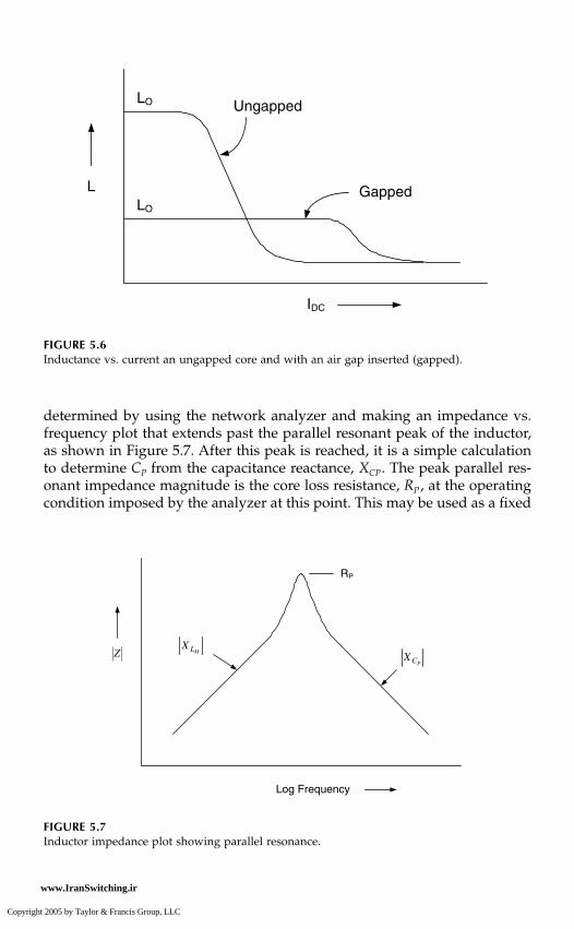
SMPS Component Models
103
determined by using the network analyzer and making an impedance vs.frequency plot that extends past the parallel resonant peak of the inductor,as shown in Figure 5.7. After this peak is reached, it is a simple calculationto determine
C
P
from the capacitance reactance,
X
CP
. The peak parallel res-onant impedance magnitude is the core loss resistance,
R
P
, at the operatingcondition imposed by the analyzer at this point. This may be used as a fixed
FIGURE 5.6
Inductance vs. current an ungapped core and with an air gap inserted (gapped).
FIGURE 5.7
Inductor impedance plot showing parallel resonance.
L
LO
LO
Ungapped
Gapped
IDC
MLX
PCXZ
RP
Log Frequency
DK_1137.book Page 103 Wednesday, June 15, 2005 11:49 AM
Copyright 2005 by Taylor & Francis Group, LLC
www.IranSwitching.ir

104
Practical Computer Analysis of Switch Mode Power Supplies
resistance figure of merit if desired, but in reality
R
P
is highly variable andmore complex.
If the model is to be used for power calculation or other detailed assess-ments, the following equations may be used to determine an operating pointvalue of
R
P
. The magnetic parameters must be brought into play here. Thecore loss curves for magnetic materials are provided by the manufacturer.Figure 5.8 shows an example of the actual loss per unit volume (it issometimes given in a per-unit-weight quantity) as a function of frequency,
FIGURE 5.8
Typical magnetic core loss curves. (Magnetics Inc., W. Material.)
DK_1137.book Page 104 Wednesday, June 15, 2005 11:49 AM
Copyright 2005 by Taylor & Francis Group, LLC
www.IranSwitching.ir

SMPS Component Models
105
f
, and the peak magnetic AC flux density variation,
B
. A fairly good accept-able expression for core loss can be approximated by Equation 5.10:
(5.10)
where
K
,
x
, and
y
are constants that can be obtained from the plot or, in someinstances, provided by the core manufacturer. (See Schmit
18
for additionalinformation.) From these curves, the large signal nonlinear value of theparameter
R
P
may be calculated for a particular inductor design with thefollowing equations. Using Faraday’s law to make the flux density,
B
, tovoltage and frequency conversion,
(5.11)
N
is the number of turns;
A
c
is the core cross sectional area; and
V
avg
is theaverage voltage of the AC waveform across the inductor. The value of
R
P isnoted as
(5.12)
The form factor, FF, of the particular wave shape provides the relationshipbetween Vrms and Vavg as shown in Equation 5.13:
(5.13)
Combining Equation 5.10 through Equation 5.13 yields the expression forRP:
(5.14)
where constant C1 is
(5.15)
The form factor, FF, is a variable and must be computed for the differentwave shapes; this will be a function of the voltage and converter duty ratio, d.Another core loss variable is temperature. Schmit18 shows a polynomialrelationship of core loss vs. temperature at a particular operating frequency
PVolume
Kf BLOSS x y=
BV
f NAavg
c
=4
RVPP
rms
LOSS
=2
FFVV
rms
avg
=
R C f V FFPy x
avgy= − −
12 2( ) ( )( )
CNA
K Volumec
y
1
4=
( )( )
DK_1137.book Page 105 Wednesday, June 15, 2005 11:49 AM
Copyright 2005 by Taylor & Francis Group, LLC
www.IranSwitching.ir

106 Practical Computer Analysis of Switch Mode Power Supplies
and flux density, but Figure 5.9 shows that core loss vs. temperature isdifferent for differing operating conditions. Thus, a core loss resistance equa-tion containing all three parameters of frequency, flux density, and temper-ature may be difficult to derive.
In some situations, a polynomial curve-fitted equation derived from acurve similar to Figure 5.9 may be used as a divider for Equation 5.14 if acore loss vs. temperature plot for operating conditions near those of theactual frequency and flux density operating conditions can be obtained. Thisrather involved method of determining RP may seem impractical and maybe so for most analysis; nevertheless, it is presented here as a possible methodof doing so if desired. In most cases, a constant figure of merit value of RP
with a third- or fourth-order polynomial divider for temperature adjust-ments per Schmit18 would be satisfactory.
5.1.3 SMPS Diode Macro
When simulating a power diode in an SMPS rectifier application, one of twoconditions must be noted: whether the diode current is continuous or pulsed.If the current is continuous or smooth, it is simply a matter of using thediode model in the conventional manner. However, when the current is
FIGURE 5.9Core loss vs. temperature for differing operating conditions.
DK_1137.book Page 106 Wednesday, June 15, 2005 11:49 AM
Copyright 2005 by Taylor & Francis Group, LLC
www.IranSwitching.ir

SMPS Component Models 107
pulsed, as in a buck–boost topology, the actual operating point of the diodeexhibits characteristics existing at the peak current and not those of theaverage current, which is the current seen to flow in the diode when one isworking with a circuit-averaged SMPS model. The goal is therefore to forcethe diode macro to exhibit peak current characteristics while conductingaverage current.
Figure 5.10a shows a somewhat typical pulsed current waveform thatmight be seen in a power diode. Figure 5.10b shows a circuit model contain-ing the ohmic resistance, RS, along with a voltage source representing theclassical diode equation voltage drop.19
(5.16)
The term kT/q is approximately 26 mV at a temperature of 298.15°K(+25°C) and η is an assigned constant between 1 and 2. The saturationcurrent, IS, is a theoretical value of current, for which VF approaches 0 whenIF is reduced to. An IS variation with temperature is the most dominantcontribution to diode temperature effects.
The goal is to make the diode conduct peak current artificially while averagedcurrent flows in the diode macro. Figure 5.11 shows a typical macro for this
FIGURE 5.10a) Typical diode pulsed current waveform. b) Typical diode forward voltage drop representa-tion.
+
RS
IF
Diode
Equivalent Circuit
iP
iAVG
d' d0
a)
b)
VkTq
IIF
F
S
= +⎛
⎝⎜⎞
⎠⎟η ln 1
DK_1137.book Page 107 Wednesday, June 15, 2005 11:49 AM
Copyright 2005 by Taylor & Francis Group, LLC
www.IranSwitching.ir

108 Practical Computer Analysis of Switch Mode Power Supplies
application. The dependent current generator is equal in magnitude to thedifference in peak and average currents. The F multiplier for iAVG is expressed as:
(5.17)
This will produce the correct desired results for dynamic and steady stateconditions. In most simulations, the model of the actual diode used is simplyinserted into the behavioral model macro.
5.1.4 Integrated Circuit Controllers
All PWM controllers have one main function: to create a desired duty ratiocontrol of the power switches in the SMPS. There may be many conditionsof control, such as normal output voltage regulation, output short circuit, orsoft start-up conditions; in any case, a duty ratio control function is required.Figure 1.10 and Figure 1.11 show the simple general schemes required forvoltage and current mode control, respectively. Figure 5.12 shows the blockdiagram of an early generation integrated circuit voltage mode PWM control-ler (UC1524A); Figure 5.13 shows it embedded in a typical application.Figure 5.14 shows the block diagram of the current mode controller(UC3825A,B) and Figure 5.15 shows this controller embedded in an exampleSMPS current mode design. As is noted each controller has several internalcomponents. These examples are representative, but are just a sample of themany different ones available.
Appendix B provides information on constructing a circuit-averagingmacro model of such a controller (UC1844) and Chapter 6 contains an SMPSexample that uses this controller. One of the thrusts of this book is to advocatethe development and use of these behavioral macromodels for commerciallyavailable and also custom PWM controllers. The macromodel developed in
FIGURE 5.11Typical diode macro for pulsed current applications.
+
iAVGVM0 V
iP
(iP-iAVG) = F x iAVG
'd
dF =
Fi i
idd
p avg
avg
=−
=′
DK_1137.book Page 108 Wednesday, June 15, 2005 11:49 AM
Copyright 2005 by Taylor & Francis Group, LLC
www.IranSwitching.ir

SMPS Component Models 109
FIGURE 5.12Block diagram of an early generation integrated circuit voltage mode PWM controller(UC1524A).
FIGURE 5.13Early generation integrated circuit voltage mode PWM controller (UC1524A) embedded in atypical application.
VIN
VIN
VIN
RT
CT
OSC
COMP
INV. INPUT
N.I. INPUT
CL (+) SENSE
CL (−) SENSE
Shutdown
EB
CB
EA
CA
VREF
GND8
10
14
13
11
121615
3
OSC CLOCKCOMP
Power toInternal
Circuitry FlipFlop
+5 VReferenceRegulator
PWMLATCH
U.V.SENSE
RAMP
6
7
9
1
2E/A
200 mV
C/L
6 V 10 k
1 k
R
T
SS
5.5 V4
5
+
+
+
−
−
+−
+12 V 1.5 A
+5 V 7 A
1.5 K 0.1
1.01 KINV IN
NI IN
COMP
2.7 K .01µF
C.L. (+)C.L. ( )
RTRSC = 0.1
820 IN4946
L1 Coupled InductorCORE:UMT
13005 .002 µF
2N222247
2N2222N3
N2
N1
T1
R118 K2 W
UT236
1 K
1 K
T2
IN914
N1
L1N1
L1N2
UES 2402
USD645C
2.2 K
CT GND
VREF
EAEB
UC1524A
4.7 K
10 k
RF18 K
200pF
10 k
D3IN914
4.7 K
AC LINE
D1IN914
D2IN914
10 K
697-4
68
C1300 µF
C2100 µF
500 µF
2200 µF
CF.01 µF
0.2 µF
UZ8710
10 V
N3N2
N4
A 438281-2 MPPN1: 13T, 18AWGN2: 29T, 18AWG
T1 Power TransformerCORE: EC35- 3C8EEN1: 124T, 24AWGN2: 16T, 28AWGN3: 14T, 20AWG
T2 Feedback TransformerCORE: 204T 250–3C8N1: 14T, 36AWGN2: 14T, 36AWGN3: 17T, 36AWG
N4: 28T, 22AWG
CACBVIN
DK_1137.book Page 109 Wednesday, June 15, 2005 11:49 AM
Copyright 2005 by Taylor & Francis Group, LLC
www.IranSwitching.ir

110 Practical Computer Analysis of Switch Mode Power Supplies
FIGURE 5.14Block diagram of the current mode controller (UC3825A,B).
FIGURE 5.15Current mode controller (UC3825A,B) embedded in an example SMPS current mode design.
Clock/LEB
RAMP
E/A OUTNI
INV
SoftStart
I LIM
VCC
GND
RTCT
(60%)
OSC
1.25 V
PWMCMPTR
Current Limit
1.2 V
0.2 V
‘B’ 16/10 V‘A’ 9.2/8.4 V
4.0 V
FaultLatch
UVLORestartDelay
OverCurrent
5 V
SD
SD
R
RestartDelayLatch
Soft-StartComplete
PWMLatch
SR
RT
250 µA
9 µA
VREFGood
InternalBias
1311
16 5.1 VVREF
1412
VREF5.1 V
On/Off
1.0 V
E/A PWR GNDOut B
Out AVC
4
56
7
3
21
8
9
15
10
VOUT+
−
+Vin
47 pf
C203K
300 pF
R1020 K
R1382 K
R93K3
R251 K
1
2
3
45
UC3825B
67
8
16
15
14
1312
1110
CR31N5820
C13150 pF
C154.7 nF
1N4148X4
3T
C17CR6USD640C
CR7USD640C
C164.7 nF 24Ω
R2324 Ω
R2024Ω
R2451Ω 1W
1.2
3.4
7.8
5.6
10 T
10 T
T1
R3 1K5
R16200 Ω
R2124 ΩL1
R18200 Ω
6.2Ω
6.2Ω
R11
R12
Q1
R4 1K
1N4148X4
25T
T2+ ~
~−
+ ~
~−
24 ΩR6
CR21N5820
IRF 640
IRF 6409
PGND
C6
C10
C111 µF
3 µF
C815 pF
C14150 pFP/O
T2
P/OT2
9
102T
11
122T
C14.7 µF
C24.7 µF
4.7 µF
C31 µF
C12560 pF
0.1 µF
C52.2 nF
−Vin
R22
DK_1137.book Page 110 Wednesday, June 15, 2005 11:49 AM
Copyright 2005 by Taylor & Francis Group, LLC
www.IranSwitching.ir

SMPS Component Models 111
Appendix B is considered to be only one approach and the reader is stronglyencouraged to use his creativity in devising other techniques.
5.2 Parasitic Resistance Effects
When an SMPS is modeled and second-order effects are to be considered,the major parasitic resistance effects of most power components are required.These parasitic resistances have many sources; the following four are repre-sentative of the ones normally considered:
• Power switch resistance• Power rectifier equivalent resistance• Inductor resistance• Input and output filter capacitor equivalent series resistances
Other component resistances, such as fuses and wiring, that are effectivelyin series with these resistances may be lumped in with them. Polivka et al.20
created the seminal paper on the topic of parasitic resistances and this is recom-mended reading. The large signal models obtained using developments fromthis paper and the expressions relating these parasitic resistances for the buck,boost, and buck–boost topologies are shown in Figure 5.16 through Figure 5.18.
FIGURE 5.16a) Buck converter with parasitics. b) Buck model with parasitics.
v
a)
b)
g
+
Q
D
L
RC
RLRT
RD
RC
v
d
vg
+
L
RC
RL+ d’RDRT/d
RCd
d
+
+
VM0 V
v
DK_1137.book Page 111 Wednesday, June 15, 2005 11:49 AM
Copyright 2005 by Taylor & Francis Group, LLC
www.IranSwitching.ir

112 Practical Computer Analysis of Switch Mode Power Supplies
FIGURE 5.17a) Boost converter with parasitics. b) Boost model with parasitics.
FIGURE 5.18a) Buck–boost converter with parasitics. b) Buck–boost model with parasitics.
v
a)
b)
g
+
Q
DL
RC
RL
RT
RD
RC
v
d
vg
+
L
RC
RL + dRT RD/d’ +RC(d/d’)
RC
v
d
d+VM
0 V
+
vg
+
LRLRT/d’
d
d
+
+
VM10 V RC
RC(d/d’)
RC
-v
-d
d+VM2
0 V
+
vg
+
Q
RC
RT
RC
-v
d
DRD
L
R
a)
b)
L
DK_1137.book Page 112 Wednesday, June 15, 2005 11:49 AM
Copyright 2005 by Taylor & Francis Group, LLC
www.IranSwitching.ir

SMPS Component Models 113
The Cuk converter with parasitic resistances is somewhat complex and notshown here, but the small signal results are presented in Polivka et al.20 Thelarge signal model may be developed in the same manner as those for thethree cases in Figure 5.16 through Figure 5.18 (see Section 6.3).
5.3 Peripheral Circuit Additions
The next series of topics will provide general information on some of themain peripheral circuits associated with SMPSs. The list is by no meansintended to be all inclusive, but it does show some of the main topicsencountered when an SMPS is modeled.
5.3.1 Input Filter
When the many functions that an input filter of an SMPS is called upon toperform are considered, it soon becomes apparent that it is one of the mostconstrained circuits in the design. A detailed computer analysis is veryessential in determining that all these constraints are satisfied. The followinglist contains many of these functions and constraints:
• The input filter limits conducted ripple current emissions onto theinput power lines (differential and common modes).
• The input filter provides RF and some measure of required audionoise voltage susceptibility rejection (differential and commonmodes).
• The filter AC output impedance must be held to less than a necessarymaximum value to ensure that the input filter instability problemdoes not exist. See Middlebrook and Cuk2 and Middlebrook.13
• The filter AC input impedance must not be allowed to produce aseries resonant dip that would violate any power source loadinglimitations.
• The filter should be able to limit the converter switching ripplevoltage on the filter output to a specified level to ensure glitch-freepower converter operation.
• The filter should limit audio susceptibility-produced resonant peaksand valleys so that: (1) undervoltage lockouts and/or regulationdropouts do not occur; (2) overvoltage (and overcurrent) componentstresses do not occur; and (3) input fuses or circuit breakers are nottripped with the increased current.
• Inductive voltage spikes must be suppressed when input power isbeing switched off.
DK_1137.book Page 113 Wednesday, June 15, 2005 11:49 AM
Copyright 2005 by Taylor & Francis Group, LLC
www.IranSwitching.ir

114 Practical Computer Analysis of Switch Mode Power Supplies
• Outrush surge current stresses must be controlled for line dropoutconditions to protect switches, relays, fuses, etc.
• Low-frequency reflected load ripple current may need to be attenu-ated by the input filter in some cases.
• High-voltage line spikes may need to be suppressed or rejected.• Proper filtering and rectification for off-line AC power sources are
required. • Size, weight, and cost limitations must be met.
Other custom requirements may need to be satisfied; however, this listprovides the general idea of the many functions and constraints of the SMPSinput filter. Figure 5.19 shows an example of an input filter that might beemployed. Appendix A considers optimal design approaches to input filterdesign.
5.3.2 Inrush Current Limiter
The inrush current limiter, as its name implies, limits surge currents into theSMPS when the input line voltage is switched on. This surge current resultsfrom the initial charging of the filter capacitors of the input filter and, sub-sequently, the output filter capacitors of the converter and load. There areseveral implementations for this function. Typically, a surge-limiting seriesresistor is inserted that is switched out after near steady state operation isachieved. Figure 5.20 shows the concept.
This switch may be a mechanical or electronic switch and may be closedafter some time delay, allowing for near steady state capacitor charge voltageto be achieved. Conversely, it may be closed at some particular charge voltagethreshold of the capacitors involved. If the voltage threshold scheme is used,a substantial amount of hysteresis must be implemented in the voltagedetector to prevent an ON/OFF oscillating limit cycle when this capacitorvoltage sags with the converter starting to draw power. As may be surmised,
FIGURE 5.19Generic SMPS low-pass input filter.
C
nC
RD
L
VIN(DC)VOUT
+
-
+
-
DK_1137.book Page 114 Wednesday, June 15, 2005 11:49 AM
Copyright 2005 by Taylor & Francis Group, LLC
www.IranSwitching.ir
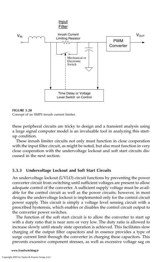
SMPS Component Models 115
these peripheral circuits are tricky to design and a transient analysis usinga large signal computer model is an invaluable tool in analyzing this start-up condition.
These inrush limiter circuits not only must function in close cooperationwith the input filter circuit, as might be noted, but also must function in veryclose cooperation with the undervoltage lockout and soft start circuits dis-cussed in the next section.
5.3.3 Undervoltage Lockout and Soft Start Circuits
An undervoltage lockout (UVLO) circuit functions by preventing the powerconverter circuit from switching until sufficient voltages are present to allowadequate control of the converter. A sufficient supply voltage must be avail-able for the control circuit as well as the power circuits; however, in mostdesigns the undervoltage lockout is implemented only for the control circuitpower supply. This circuit is simply a voltage level sensing circuit with aprescribed hysteresis, which enables or disables the control circuit output tothe converter power switches.
The function of the soft start circuit is to allow the converter to start upwith a duty ratio that is near zero or very low. The duty ratio is allowed toincrease slowly until steady state operation is achieved. This facilitates slowcharging of the output filter capacitors and in essence provides a type ofsurge current limit through the converter in charging these capacitors. Thisprevents excessive component stresses, as well as excessive voltage sag on
FIGURE 5.20Concept of an SMPS inrush current limiter.
PWMConverter
InputFilter
VIN VOUT
Time Delay or VoltageLevel Switch on Control
Inrush CurrentLimiting Resistor
Mechanical orElectronicSwitch
DK_1137.book Page 115 Wednesday, June 15, 2005 11:49 AM
Copyright 2005 by Taylor & Francis Group, LLC
www.IranSwitching.ir

116 Practical Computer Analysis of Switch Mode Power Supplies
the input filter capacitors, which could result in resetting of the UVLO andinrush current limiting circuits. In such cases, chaotic and possibly destruc-tive circuit operation could occur.
Soft start control circuits of this type are almost always implemented byslowly charging a capacitor from 0 V and having the pulse width modulatortrack this voltage. This signal is diode ORed with the normal feedbackcontrol and, at some point, the control signal takes over the PWM controland provides normal output regulation. Figure 2.4a and Figure 2.4b show aconceptual example of how a coordinated inrush limiter, input filter, UVLO,and soft start circuit may be implemented.
5.3.4 Power Factor Correction Circuits
When operating from an off line AC power source, a rectifier and a low-passfilter circuit are required to convert the AC input to a DC voltage that canbe used by the SMPS power converter. The filter can be an inductive orcapacitive input filter. In either case, the rectifier/filter distorts the inputcurrent waveform, resulting in a less than unity power factor and harmonicdistortion of the input current waveform. Most SMPSs today use a capacitiveinput filter for a number of practical reasons, such as cost and weight;unfortunately, it generally produces the worst case of distortion and powerfactor.
The solution used to reduce these drawbacks is to include an activepower factor correction, PFC, circuit in the design. The existing technologyfor PFC calls for a circuit to be inserted between the input voltage rectifierand what would otherwise be a capacitive input filter. Figure 5.21 showsthe input current wave shapes for the uncorrected capacitive input filterand the input current corrected with a PFC circuit. From a power systempoint of view, it is desired that the input current waveform have the sameand in-phase sine wave shape as the source voltage or, in other words,have a unity power factor. This results in the minimum RMS current andtherefore the lowest transmission losses from the power source. To accom-plish this, a uniquely controlled power converter is inserted to provide thedesired controlled input current waveform.
The most widely used power converter topology for this application is theboost converter operating at a frequency much greater than that of the ACinput power. The buck–boost converter and its variants such as the Cuk4
and SEPIC21 topologies have also been used successfully. When the boostconverter is used, the output DC voltage should always be greater than theexpected peak of the AC input voltage to maintain control. The buck–boosttopologies, however, may operate with the output voltage greater or lessthan the peak AC input. Todd22 provides a very detailed look at the conceptsand design of a PFC circuit using the boost topology and is recommendedreading.
DK_1137.book Page 116 Wednesday, June 15, 2005 11:49 AM
Copyright 2005 by Taylor & Francis Group, LLC
www.IranSwitching.ir

SMPS Component Models 117
An active PFC circuit has two primary functions: to control the inputcurrent, forcing it to assume the same wave shape as the rectified sinewave, and to regulate its output DC voltage. Figure 5.22 shows a concep-tual circuit using the boost topology. Shown are two basic control loopsidentified as Loop 1 and Loop 2. Loop 1 is the control loop for the inductor(and input) current and, when it is closed, it is embedded within theoutput voltage regulation control, Loop 2. At first glance, the control seemssomewhat nonlinear with the multiplier, squarer, and divider circuits, butthese nonlinear circuit effects are compensatory and tend to cancel out.Also, the bandwidths are sufficiently separated so that linear control canbe assumed.
The multiplier accepts the current control, VC, from the divider and mul-tiplies (or modulates) it with the rectified sine wave shape from VIN, whichin turn forces IIN to assume the desired sine wave shape. Loop 1 therefore
FIGURE 5.21Rectified input currents for a capacitive input filter.
0Volts
Input VoltageHalf Sine Wave
UncorrectedInput Current
Power Factor CorrectedInput Current
DK_1137.book Page 117 Wednesday, June 15, 2005 11:49 AM
Copyright 2005 by Taylor & Francis Group, LLC
www.IranSwitching.ir

118P
ractical Com
puter Analysis of Sw
itch Mode P
ower Supplies
FIGURE 5.22Conceptual power factor control using boost converter topology.
uC tnerroL po
lortnoC
-+
-+Mult reilpi
oL w P a ssliF t re
erauqS rx( 2)
viD ideroV egatl
orrE rpmA
VC
VIN )GVA(
I NES ES
I OC TN OR L
I NI
1# pooL
ooL 2# p
2IN )GVA(V
VE
+
-
oTMS SP
rewoPtS ega
V FER
CAtupnI
VO
d
DK
_1137.book Page 118 Wednesday, June 15, 2005 11:49 A
M
Copyright 2005 by T
aylor & Francis G
roup, LL
C
www.IranSwitching.ir

SMPS Component Models 119
needs to have a relatively wide bandwidth and sufficient gain to track thecontrol signal ICONTROL and appear as a constant gain block insofar as Loop2 is concerned. Incidentally, the inductor current control loop may be aconventional fixed frequency peak current mode control, but more accuratecurrent control and better power factor performance are achieved with anaverage current control scheme.27 Also, with average current control, thecurrent slope compensation ramp normally required for constant frequencypeak current control is not required. This is a real advantage because theconverter duty ratio is required to vary over a wide range when trackingVIN. Ramp stability can sometimes be difficult under these circumstances.
This average current control loop assumes the properties of a voltage modecontrol and must be dealt with accordingly. Also, continuous and discontin-uous modes of converter operation are acceptable. (In the continuous mode,do not forget the right-half plane zero.) For the moment, hold the controlsignal, VC, constant and increase the input voltage, VIN. Note that the inputvoltage has increased, and the input current has also increased by the highermodulated peak of ICONTROL. In other words, the input power increases as thesquare of the input voltage. To prevent this input voltage change frominfluencing the output voltage, VO, which has a constant power load, thecontrol signal must be obtained by dividing the voltage error amplifieroutput signal, VE, by the square of the average input voltage, VIN. This isfacilitated by the low-pass filter and the squarer circuits of Figure 5.22.
The bandwidth of the output voltage control loop, Loop 2, must be con-siderably lower than the line frequency so that it does not attempt to trackand negate the desired modulation of ICONTROL. On the other hand, it mustbe as wide as is practical to provide the maximum amount of transient linerejection. In practice, it appears that a bandwidth of about one-sixth of therectified line frequency is typical, depending on the desired power factorand harmonic distortion specifications. Another scheme that can improvetransient performance and permit an effective wider voltage loop bandwidthis to use a sample-and-hold scheme to update VIN(avg)
2 at the end of everyline-rectified cycle.
Several other practical considerations associated with this concept arenoted in Todd.22 Other PFC schemes have been used successfully;Andreycak23 shows one that operates at critical inductor current and has asimpler control scheme using a variable frequency, controlled ON time con-verter. Unfortunately, component stresses generally prevent operation atpower levels greater than 500 W for this scheme with today’s technology.
The standards of power factor and total harmonic distortion can be varieddepending on the usage circumstances. Kassakian24 has shown a useful andinteresting relationship between power factor, PF, and total harmonic dis-tortion, THD, as:
(5.18)PFTHD
=+
11 2
DK_1137.book Page 119 Wednesday, June 15, 2005 11:49 AM
Copyright 2005 by Taylor & Francis Group, LLC
www.IranSwitching.ir

120 Practical Computer Analysis of Switch Mode Power Supplies
5.3.5 Multiple Outputs
When a power converter with multiple outputs is modeled, some specialconsiderations must be noted. Figure 2.2 shows a typical example of apush–pull converter with split secondary multiple outputs. Of course, anynumber of multiple outputs can be added to the power transformer. Also,some or all of them may have coupled inductors.
First, consider a case of multiple outputs for a buck topology in whichsome outputs are in the continuous mode and some are in the discontinuousmode. Figure 5.23 shows a conceptual way of modeling the two outputs ofthe converter of Figure 2.2 when the output inductors are not coupled. (Whenoutput inductors are coupled together, all of these coupled loads theoreticallyfunction together as continuous or discontinuous, regardless of the individ-ual loads. When these circuits are modeled, the outputs should be paralleledat the inductor input.) Note that the mode of each individual output is
FIGURE 5.23Modeling example of multiple output converter with continuous output or discontinuousconduction mode.
F2
LO2
+
+
+vO2
LO1
+
+
+vO1
F1
+
-
VIN
R2CO2
CO1R1
ConductionMode Detector
DK_1137.book Page 120 Wednesday, June 15, 2005 11:49 AM
Copyright 2005 by Taylor & Francis Group, LLC
www.IranSwitching.ir

SMPS Component Models 121
determined by its individual conduction mode-detecting circuit as it loadsthe power transformer.
If the expected mode of all outputs is known at the outset, then the modelcan be simplified by eliminating the mode-detecting circuits and simplyreflecting the output circuits or loads — whether continuous or discontinu-ous — to the transformer primary by the current sources F1 and F2. Inci-dentally, when synchronous rectifier outputs as described in Section 5.3.7are used with conventional rectifiers on other outputs, this mixed continu-ous/discontinuous situation may still result.
Now look at this same model example with parasitic effects. Figure 5.24shows the basic circuit and Figure 5.25 shows the circuit-averaged model forthis circuit that may be used in a computer model. The model developmentis not shown here, but may be derived using the methods indicated in Polivkaet al.20 Another example showing a split secondary plus or minus outputpush–pull buck converter with parasitic resistances is shown in Figure 5.26.The accompanying circuit-averaged model is shown in Figure 5.27. Again, thederivation is not shown but may be derived using the methods in Polivkaet al.20
FIGURE 5.24Multiple output push–pull buck converter with parasitic resistances.
L1
RC1
RL1
RO1
C1
v1
RD1
RS1 RD1
RS1
L2
RC2
RL2
RO2
C2
v2
RD2
RS2 RD2
RS2
N2
N3
N2
N3
+
RP
RP
vA N1
N1
DK_1137.book Page 121 Wednesday, June 15, 2005 11:49 AM
Copyright 2005 by Taylor & Francis Group, LLC
www.IranSwitching.ir

122 Practical Computer Analysis of Switch Mode Power Supplies
FIGURE 5.25Circuit-averaged model of the converter in Figure 5.24.
FIGURE 5.26Plus or minus output push–pull buck converter with parasitic resistances.
vA
L1
RC1
RL1
RO1
C1
v1
+
+O V
L2
RC2
RL2
RO2
C2
v2
+
+
( ) ⎟⎠⎞⎜
⎝⎛
⎟⎠⎞⎜
⎝⎛
++
2d1
RR D2S2
⎟⎟⎠
⎞⎜⎜⎝
⎛
⎟⎟⎠
⎞⎜⎜⎝
⎛
1
3
NN
d
O V
+
d
RP
( ) ++
2d1
RR D1S1
1
2
NN
d
1
2
NN
d1
3
NN
d ⎟⎟⎠
⎞⎜⎜⎝
⎛
⎟⎟⎠
⎞⎜⎜⎝
⎛
RS
RS
N2
N2
+
RP
RP
vA N1
N1
RD1
RD1
L1
RC1
RL1
RO1
C1
+v1
L2
RC2
RL2
RO2
C2
-v2
RD2
RD2
DK_1137.book Page 122 Wednesday, June 15, 2005 11:49 AM
Copyright 2005 by Taylor & Francis Group, LLC
www.IranSwitching.ir

SMPS Component Models 123
5.3.6 Postregulated Output Circuits
In many instances, the outputs of an SMPS are not directly regulated orcontrolled by the circuitry that controls the PWM of the main power converter.This is always the case when multiple outputs (discussed in Section 5.3.5) areused. When this occurs and it is desired to have better regulation than isnormally obtainable, a postregulator is inserted between the particular SMPSoutput and load.
In practice, postregulation can be provided in two ways. One may simplyimplement a dissipative linear voltage regulator; this may be acceptable forlow-power outputs, but would ordinarily be prohibitive for higher powers.The more efficient option would be simply to insert a second post-SMPS. ThisSMPS may be implemented by a conventional converter design as describedin Chapter 1; however, a more viable approach is to take advantage of theexisting main converter switching action and use a magnetic amplifier scheme.Mammano and Mullett25 provide information on the fundamentals of usingmag-amps for this application. Magnetic amplifier design is a somewhat spe-cialized endeavor and many subtleties are involved when the magnetic non-linearities and reset requirements are addressed. Figure 5.28 shows aconceptual circuit of a two-output forward converter SMPS in which oneoutput is directly regulated by the main PWM controller and the second outputis controlled by a post-mag-amp regulator. Voltage waveforms are also shown.
When these types of mag-amp regulators are analyzed, it is importantto recognize that they are essentially buck topology SMPSs in themselves.The model is created and generally analyzed in the same way as for any
FIGURE 5.27Circuit-averaged model of the converter in Figure 5.26.
L1
RC1
RL1
RO1
C1
+vo
+
+O V
L2
RC2
RL2
RO2
C2
-vo
++
O V
dRS
2
Rd' S
dRS
vA
+⎟⎟⎠
⎞⎜⎜⎝
⎛⎟⎟⎠
⎞⎜⎜⎝
⎛
⎟⎟⎠
⎞⎜⎜⎝
⎛
1
2
NN
d
dRP
1
2
NN
d
1
2
NN
d
1
2
NN
d
⎟⎠⎞⎜
⎝⎛
⎟⎠⎞⎜
⎝⎛
+
2d1
RS
+
2d1
RS
DK_1137.book Page 123 Wednesday, June 15, 2005 11:49 AM
Copyright 2005 by Taylor & Francis Group, LLC
www.IranSwitching.ir

124 Practical Computer Analysis of Switch Mode Power Supplies
FIGURE 5.28Conceptual forward converter SMPS with post-mag-amp regulator. (R.A. Mammano and C.E.Mullett, Unitrode Application Note U-109.)
iP
V1orV3
V2
V4
V5
V1
PWM ControlUC1838
V1 V2
V3 V4 V5
iP
V+ 12V10A
5V50A
DK_1137.book Page 124 Wednesday, June 15, 2005 11:49 AM
Copyright 2005 by Taylor & Francis Group, LLC
www.IranSwitching.ir

SMPS Component Models 125
conventional SMPS, with one main exception: the gain and a pronouncedphase delay associated with the magnetic modulator. Figure 5.29, excerptedfrom Mammano and Mullett,25 shows a typical regulator control loop.
5.3.7 Synchronous Rectifier Circuits
Synchronous rectifiers are generally used in low output voltage, high currentpower converters to replace conventional diode rectifiers when the highest
FIGURE 5.29Typical mag-amp postregulator control loop. (R.A. Mammano and C.E. Mullett, UnitrodeApplication Note U-109.)
VREF
-
+
MA
L
C
R
RLOAD
Filter and Modulator
Amplifier
VM
ControlLoop
DK_1137.book Page 125 Wednesday, June 15, 2005 11:49 AM
Copyright 2005 by Taylor & Francis Group, LLC
www.IranSwitching.ir

126 Practical Computer Analysis of Switch Mode Power Supplies
level of efficiency is desired. They almost always use power MOSFETswitches to accomplish this. When switch mode power supplies containingsynchronous rectifiers are analyzed, a few things should be stated. The mostfundamental is that a continuous mode of operation is always achieved andthe discontinuous mode is practically nonexistent. This is true regardless ofthe magnitude of the load current; it can be zero or it may even be negative.In some designs, regenerative load current may be sent back to the powersource. This makes it possible for a unique set of converters known asbidirectional power converters. One application is for achieving a controlledcharging and discharging for systems containing batteries. Another applica-tion may be when motor control systems are powered with regenerativecapabilities. Power amplifiers with AC output voltages and currents are alsoa very important application.
When these bidirectional concepts are used, the PWM control circuits mayhave some unique properties. For example, the battery charge and dischargepower converter may be a buck topology with power flowing in one direc-tion and a boost topology with power flowing in the other direction. Thecontrol circuit must be able to adapt to the required control algorithm forboth directions.
5.3.8 Energy Storage Systems
Energy storage peripheral circuits are implemented to hold up and maintainoutput power when the main input power source drops out. These dropoutsmay be relatively short transient interruptions, which can use capacitiveenergy storage, or lengthy or steady state dropouts requiring a backupbattery or some other alternate power source. (These steady state backupsystems are generally referred to as uninterruptible power supplies or UPS.)A control circuit is generally required to deal with these situations.
In almost all of these systems, the energy from the storage system isinjected into the power supply at the input to the converter as opposed tothe output. This is done for a number of practical reasons such as using thepower converter/regulator to maintain output regulation and also single-point energy storage for multiple output converters. In most cases, moreefficient energy storage and better performance are generally achieved whenenergy is injected at the input.
For very short transient dropouts, the normal input filter may provideenough energy storage and thus nothing extra added to the design exceptmaybe a little more capacitance at the input. However, in cases in which thisis insufficient, an additional capacitance storage bank and its accompanyingcontrol circuit are required. Figure 5.30 shows one approach to this problem.The capacitor bank is self-charged or “bootstrapped” from the main con-verter to a voltage higher than the normal DC input voltage in most casesby a simple resistor and rectifier circuit. When a line dropout occurs, a lowDC input voltage is sensed and activates the discharge controller, allowingfor a controlled energy transfer of the energy from the capacitor bank into
DK_1137.book Page 126 Wednesday, June 15, 2005 11:49 AM
Copyright 2005 by Taylor & Francis Group, LLC
www.IranSwitching.ir

SMPS Component Models 127
the main power converter input. In most cases this, is a simple voltageregulator attempting to regulate the DC input voltage. It may be a switchingor a linear regulator, but will probably be the latter for simplicity and costreasons.
When this approach is used with a DC power source, a blocking diodemay be deemed necessary at the input to prevent loss of the stored energyback to the failed power source. This diode will lower the overall SMPSefficiency and must be taken into consideration. A controlled MOSFETswitch may be used in some lower voltage and/or power applications inlieu of this blocking diode to increase the efficiency. Off-line applications donot have this problem because the input rectifiers provide the blockingfunction.
For outright total input power failure or extra long transient dropouts inwhich the capacitance approach is unfeasible, a battery backup system isrequired. The battery voltage is generally lower than the normally expectedDC input voltage and is simply diode ORed into the input; it provides powerwhen the source voltage drops out (see Figure 5.31). The battery is generallykept charged from the input power source by its own charger for properbattery conditioning. Battery chargers may also be linear or switching reg-ulators and, in general, will be a constant current supply with some sort oftrickle charge condition set up, possibly when a predetermined charge volt-age is reached. Conversely, the charger may simply just go into a voltage
FIGURE 5.30Capacitive energy storage system.
PowerConverter
DischargeController
+
-
VDCInput
ToOutputs
BlockingDiode
EnergyStorage
Capacitor
DK_1137.book Page 127 Wednesday, June 15, 2005 11:49 AM
Copyright 2005 by Taylor & Francis Group, LLC
www.IranSwitching.ir

128 Practical Computer Analysis of Switch Mode Power Supplies
regulation mode at some peak charge voltage. When a switching powerconverter is used, it would most likely have a buck topology and use currentmode control because this would be very desirable for constant currentoutputs.
5.4 Summary
This chapter has presented concepts and some development approaches tocreating the real-world circuit component models necessary when a higherthan fundamental level of SMPS analysis is desired. Also, a practical repre-sentation of most of the peripheral circuits generally associated with SMPSshas been presented along with some comments on modeling them for acircuit-averaged analysis. Of course, other peripheral circuits exist, but hope-fully this chapter can guide the reader in a way that will make it possiblefor him to develop his concepts and circuit models.
FIGURE 5.31
VDCInput
ToOutputs
PowerConverter
BatteryCharger
BlockingDiode
StorageBattery
+
−
DK_1137.book Page 128 Wednesday, June 15, 2005 11:49 AM
Copyright 2005 by Taylor & Francis Group, LLC
www.IranSwitching.ir

6
Analyzing the Advanced SMPS Model
Chapter 4 considered most of the fundamental kinds of DC and AC analysisthat one might encounter when analyzing the various properties of a verybasic buck switching regulator. These were for the static power converterwith no duty ratio control, the voltage mode controlled switch mode powersupply (SMPS), and the current mode controlled SMPS. This chapter willcontinue with the general analysis theme of that chapter and consider themore advanced or comprehensive detailed analysis methods. These willinclude large signal transient analyses as well as the DC and AC analysismethods. To be on firm ground, the reader should consult some of the numer-ous references
14,24,26
regarding the fundamentals of switch mode power sup-plies and arm himself or herself with as much basic knowledge as is possible.
First, the use of the pulse width modulator controller macromodel devel-oped in Appendix B will be demonstrated. Next, the analysis of a flyback(buck–boost) converter switch mode power supply taken from a widely pub-lished application note will be considered. This will encompass an advancedpractical circuit topology. Following this, a low-output voltage buck converteralong with its parasitic resistance effects will be presented. This model canbe used for modeling resistances drops in series power paths as well asassisting in determining power converter efficiencies. Finally, a buck con-verter SMPS with some interesting large signal analysis results is shown.
6.1 Pulse Width Modulator (PWM) Controller Macromodel
When a computer analysis of an electronic circuit is performed, a practicalapproach may be to develop macromodel building blocks representing specificcomplex functions. When an SMPS that uses a commercially available integratedcircuit controller is analyzed, it can be very useful to utilize a behavioral mac-romodel for this controller. These controllers all perform the function of PWMcontrol and may sometimes be quite complex. Appendix B shows the generalmethodology for developing a
circuit-averaging
SMPS controller macromodel.As a point of departure, the technique of using a controller macromodel
to provide PWM control of a very basic power converter will be illustrated.
DK_1137.book Page 129 Wednesday, June 15, 2005 11:49 AM
Copyright 2005 by Taylor & Francis Group, LLC
www.IranSwitching.ir

130
Practical C
omputer A
nalysis of Switch M
ode Pow
er Supplies
FIGURE 6.1
Basic current mode SMPS with UC1844 macromodel controller.
2LHµ 04
3CFµ 0002 4C
.0 Fµ 1
3R2.0 Ω
I OL DA
+
NIV81 V 03-
1LHµ 05
1C571 Fµ C2
Fµ 01
1R0.1 Ω
+
d
d
+
+
+N
9
8
7
65
2
41
3
gV V
K
1D
2D
DX 3
i( DLI )
i( DL )
1E
MV 1V 0
MV 3V 0
d
MV 2V 1
1G
2F1
Po ew oC r evn r ret
RV FE
CCVFV B
PMOC
GV
V
d
ESI N ES
LFRSTCMDNG
FR B001 K
ARK02
BRK02
DRK5
FC.0 Fµ 10
RCFp 01
CX ONT4481CU
FI NES1
NESR1
d
01
11
21
05
31
8
(V )d
DLG
DLIG
DK
_1137.book Page 130 Wednesday, June 15, 2005 11:49 A
M
Copyright 2005 by T
aylor & Francis G
roup, LL
C
www.IranSwitching.ir

Analyzing the Advanced SMPS Model
131
The basic current mode converter of Chapter 4 will be used, along with theUC1844 controller developed in Appendix B to regulate a DC output voltageof 10 V. Figure 6.1 shows the basic SMPS model to be analyzed. Two largesignal transient analyses showing line and load regulation are demonstrated.A PSPICE netlist, labeled Netlist 6.1, is used for these simulations.
NETLIST 6.1
BUCK CONVERTER CURRENT MODE ANALYSIS (10.0 V0UT) NETLISTFIGURE 6.1*.OPTIONS STEPGMIN ITL4=40 .NODESET V(13)=.1 V(1)=10 V(8)=30 V(D)=.33************************************************************************************* SOURCE-LOAD CONFIGURATION FOR LINE REGULATION ANALYSIS** (FIGURE 6.2)VIN N 0 PULSE(1U 30 .1 10 10 1M)ILOADDC 1 0 DC 1.TRAN 50M 40 0 5M ************************************************************************************* SOURCE-LOAD CONFIGURATION FOR LOAD REGULATION ANALYSIS** (FIGURE 6.3)*VIN N 0 DC 30*ILOAD 1 0 PULSE(0 4 1.5 1)*.TRAN 1M 4 0 1M *************************************************************************************POWER CONVERTER MODEL*C4 1 0 .1UC3 1 3 2000UR3 3 0 .2**L = 40U*TS = 10U*N = TRANSFORMER TURNS RATIO***GLD 2 K VALUE = V(d)**2*N*(V(8)/V(1))*(V(8)-V(1))*(TS/(2*L))GLD 2 K VALUE = V(d)**2*1*(V(8)/V(1))*(V(8)-V(1))*(10U/(2*40U))VM3 K 1XD3 2 1 DIDEALL2 4 2 40U**E1 4 5 VALUE = V(8)*V(d)*NE1 4 5 VALUE = V(8)*V(d)*1VM1 0 5GILD 6 7 VALUE = I(VM3)*V(1)/V(8)**G1 0 6 VALUE = I(VM1)*V(d)*NG1 0 6 VALUE = I(VM1)*V(d)*1
DK_1137.book Page 131 Wednesday, June 15, 2005 11:49 AM
Copyright 2005 by Taylor & Francis Group, LLC
www.IranSwitching.ir

132
Practical Computer Analysis of Switch Mode Power Supplies
D1 6 7 D2D2 0 6 D2.MODEL D2 D VM2 7 0 DC 1F2 8 0 VM2 1RVM2 7 0 1KC2 8 0 10UC1 8 9 175UR1 9 0 1L1 N 8 50U ************************************************************CONTROL CIRCUIT MODEL*FISEN 0 13 VM1 1RISEN 13 0 1CF 10 12 .001URFB 12 11 100KCR 10 11 10PRA 11 1 60KRB 11 0 20KRD 50 0 5KXCONT 8 50 11 10 13 1 8 d 0 UC1844*************************************************************UC 1844 PWM CONTROLLER CIRCUIT AVERAGING MACRO.SUBCKT UC1844 VCC 3 4 COMP 6 7 8 d GND* VCC VREF VFB COMP ISENSE V VG d GND**NOTE: ALL SIGNAL INPUTS MUST REFERENCED TO THE UC1844 GND XUVLO VCC UVLO GND UVLOXREF UVLO VCC 3 VREF/2 GND REFXERRAMP 4 VREF/2 VCC COMP GND ERRAMPXDRC COMP d 6 7A 8A UVLO GND DRC**DEPENDENT GENERATORS FOR GROUND ISOLATION IF DESIREDEVG 8A 0 8 GND 1EV 7A 0 7 GND 1.ENDS UC1844*.SUBCKT DRC 1 d 8 9 10 14 GND* COMP d ISENSE V VG UVLO GNDVBK 1 1A DC 2 R1 1A C 200KR2 C GND 100KX1 C 3 DIDEALX2 GND C DIDEALVLIM 3 GND DC 1RCONV1 6 0 1GRCONV2 7 0 1GRCONV3 4 0 1G*REL 10 9 1E8GL 0 11 10 9 1D1L 11 12 DX
DK_1137.book Page 132 Wednesday, June 15, 2005 11:49 AM
Copyright 2005 by Taylor & Francis Group, LLC
www.IranSwitching.ir

Analyzing the Advanced SMPS Model
133
D2L 0 11 DXRLMIN 12 13 1VLMIN 13 0 1U*DX1 4 0 DXDX2 7 4 DXDX3 6 7 DX***IDRMAX VALUE = MAX LIMITED DUTY RATIOIDRMAX 7 6 DC .48DX4 0 6 DXDX5 6 6A DXVMD 6A 0EMD d 0 VALUE = I(VMD)*V(14)+1PRMD d 0 1.MODEL DX D IS=1E-12**L = 40U*RF = 0.3*TS = 10U*MC = .3E6***GCM 4 7 VALUE = (V(C)-RF*V(8))/((TS*RF)/(2*L))*(2*MC*L+V(12)))GCM 4 7 VALUE = LIMIT((V(C)-0.3*V(8))/((10U*0.3)/(2*40U)*(2*.3E6*40U+V(12))),0,1)***GDCM 0 4 VALUE = V(C)/((TS*RF/L)*(MC*L+V(12))GDCM 0 4 VALUE = LIMIT(V(C)/((10U*0.3/40U)*(.3E6*40U+V(12))),0,1)*.ENDS DRC*.SUBCKT UVLO VCC UVLO GND* VCC UVLO GNDRIN VCC 2 1KISUP 2 GND 1MXSUP GND 2 DIDEALG5 VCC GND VALUE = .01*V(UVLO,GND)** G1 AND G2 SET UVLO START AND STOP LEVELS RESPECTIVELY** START = 17** STOP = 10G1 0 3 TABLE V(VCC,GND) = (0,0) (17,0) (18,20)G2 3 0 TABLE V(VCC,GND) = (9,20) (10,0) (17,0)CG2 3 0 20NR1 3 0 1E3G3 0 4 3 0 1G3HYST 0 4 VALUE = -100U+200U*V(UVLO,GND)CHOLD 4 0 20NG4 GND UVLO 4 GND 1**VOVRD TO BE INSERTED FOR UVLO OVERRIDE*VOVRD UVLO GND DC 1RG4 UVLO GND 1CG4 UVLO GND 1NX5 GND UVLO DIDEALX1 3 5 DIDEALX2 6 3 DIDEALX3 4 5 DIDEAL
DK_1137.book Page 133 Wednesday, June 15, 2005 11:49 AM
Copyright 2005 by Taylor & Francis Group, LLC
www.IranSwitching.ir

134
Practical Computer Analysis of Switch Mode Power Supplies
X4 6 4 DIDEALVP 5 0 DC 1VN 0 6 DC 1.ENDS UVLO**5.0 VOLT REFERENCE MACRO.SUBCKT REF UVLO VCC VREF VREF/2 GND* UVLO VCC VREF VREF/2 GND* EIN 2 3 VCC GND .46E-3RVT 3 4 .32 TC=0.2E-3IVT GND 3 DC 3.125 VT GND 4 DC 1V5 1 2 DC 4.99342FUVLO 1 GND VMR 1EUVLO VREF 9 VALUE = V(1,GND)*V(UVLO,GND)VMR GND 9EVREF/2 VREF/2 GND VREF GND .5.ENDS REF**ERROR AMP MACRO.SUBCKT ERRAMP 6 7 8 1 GND * VIN VIP VCC OUTPUT GNDRIN 5 7 1MEGEPSRR 6 5 VALUE = (V(8)-15)*3E-4IBIAS GND 5 .3UGA GND 2 7 6 1KRG 2 GND 30CG 2 GND 0.159MVNC 4 GND DC 1DN 4 2 D1VPC 3 GND DC 5DP 2 3 D1RO 1 2 3KRPS 8 0 1E8.ENDS ERRAMP.MODEL D1 D IS=1E-9*******************************************************.SUBCKT DIDEAL 1 2VAS 1 3 DC -1uD1 3 2 DD2 3 4 DD3 4 2 D1FAS 4 2 VAS 1.MODEL D D IS=1E-6 EG=0 XTI=-4.MODEL D1 D EG=0 XTI=0CC 1 2 .1P.ENDS DIDEAL*.PROBE.END
DK_1137.book Page 134 Wednesday, June 15, 2005 11:49 AM
Copyright 2005 by Taylor & Francis Group, LLC
www.IranSwitching.ir

Analyzing the Advanced SMPS Model
135
Figure 6.2 shows the representative line voltage regulation curve of the basic10-V output SMPS with a constant current 1.0-amp load. Note that the outputvoltage remains at 0 V until the input voltage rises to the undervoltage lockout(UVLO) level of 17 V. At this point, the converter is allowed to switch and theduty ratio immediately rises to its maximum clamped value of
d
= 0.48 withthe output voltage rising to a level of around 8.2 V. As the input voltage isfurther increased, the output voltage rises accordingly until the threshold ofregulation is reached at an input voltage of about 22 V. At this point, thefeedback control loop takes over and regulates the output voltage to 10 V bycontrolling the duty ratio as the input voltage is further increased to 30 V. Nownotice that, when the input voltage is reduced from the 30-V level downwardand then drops below the 22-V level, the output voltage eventually decreasescorrespondingly. However, due to the hysteresis in the UVLO, the convertercontinues functioning down to an input voltage of 10 V before shutting down.
Figure 6.3 shows the representative load regulation characteristic with aconstant 30.0-V input voltage. The overload characteristic with the output-regulated 10 V starts to drop at a load current of approximately 1.5 amps. Thisoccurs when the control voltage,
V
C
, in the UC1844 saturates high at its maxi-mum clamped value of approximately 1 V. (This is the current sense comparatorinput in the actual UC1844.) The power supply is therefore current limited atthe load current corresponding to this clamped 1.0-V value of control voltage.
Some comments might be made here about Netlist 6.1. Note commententries. Those at the beginning parts of the netlist indicate the correct stimuliand commands to be used for a
desired
analysis
. Here, only one analysis set isactivated at a time by removing the asterisk at the beginning of the line entries.
FIGURE 6.2
Line regulation characteristic of the basic 10-V output current mode SMPS.
10 V
5 V
−2 V
1.0 V
0.5 V
0 V
0 V 5 V 10 V 15 VV(N)V(D)
SEL>
>
Max Clamped DutyRatio = 0.48
Duty Ratio
Input Voltage
Input Voltage
Threshold of Regulation
Vout
V(1)
20 V 25 V 30 V
DK_1137.book Page 135 Wednesday, June 15, 2005 11:49 AM
Copyright 2005 by Taylor & Francis Group, LLC
www.IranSwitching.ir

136
Practical Computer Analysis of Switch Mode Power Supplies
Follow any instructions indicated shown for that particular analysis. Othercomment lines shown further down and throughout the netlist indicate theelements or equation operations that must be set up for a
particular design
.These parameter inputs must be inserted for
both
the converter model andthe UC1844 controller macromodel.
A word of caution from the outset regarding the difficulties that may beencountered when running these simulations: due to lack of convergenceproblems, they can sometimes require considerable experimentation. Thesemodels have regenerative latching circuits, as well as several nonlineardependent equations with points of discontinuity, and can sometimes haveconvergence problems in DC and transient simulations. All simulations inthis book were run on a personal computer using the relatively low-costPSPICE
™
software. More expensive workstation software simulators, suchas SABER
™
, ACCUSIM
™
, and others, generally have less problems. Oneshould familiarize himself with all the OPTIONS and time step controlaspects of the software used in order to be able to overcome these conver-gence problems.
6.2 Practical Flyback SMPS Analysis
The schematic diagram of a practical flyback SMPS example taken fromUnitrode Corporation Application Note No. 96A is shown in Figure 6.4. Thisexample is selected because it is typical of many commercial SMPSs used in
FIGURE 6.3
Load regulation characteristic of the basic 10-V output current mode SMPS.
5 V
10 V
0 V
2.0 V
1.0 V
0 V
I (ILOAD)
Vin = 30.0 Vdc
l Load
l Load
V(XCONT.XDRC.C)
V(1)
V(D)
SEL>
>
4.0 A3.0 A2.0 A1.0 A
Control Voltage, VC
Current Limit Knee
0 A
Duty Ratio, d
Vout
DK_1137.book Page 136 Wednesday, June 15, 2005 11:49 AM
Copyright 2005 by Taylor & Francis Group, LLC
www.IranSwitching.ir

Analyzing the Advanced SMPS Model
137
electronic equipment today. The power supply specifications are as indicatedin Figure 6.4.
A brief description of the power supply is as follows: the flyback convertersection of the power supply is composed of the power switch,
Q
1; trans-former,
T
1; rectifier diodes,
D
6 through
D
8; and output filter capacitors,
C
10through
C
13. The applied AC input power of 117 Vac is rectified by a fullwave bridge, represented by the block,
D
1, and then filtered by capacitor
C
1. This gives a nominal DC voltage of about 165 V as input voltage to theconverter section. The PWM controller, UC1844, obtains the peak inductorcurrent information by sensing the voltage across resistor
R
10. In this case,the peak switch current is the same as the desired peak inductor current. Aseparate feedback winding labeled
N
C
provides not only the feedback voltageregulation signal, but also the power saving bootstrap voltage to power the
FIGURE 6.4
Practical flyback SMPS analysis example.
R15 Ω1 W
117 VAC
D1
VAROVM 68
C1250 µF250 V
C60.0022 µF
Power Supply Specifications1. Input Voltage:2. Line Isolation:3. Switching Frequency:4. Efficiency @ Full Load:
95 VAC to 130 VAC (50 Hz/60 Hz)3750 V40 kHz70%
5. Output Voltage:A. +5 V, ±5%: 1 A to 4 A load
Ripple voltage: 50 mV P-P Max.
B. +12 V, ±3%: 0.1 A to 0.3 A load Ripple voltage: 100 mV P-P Max.
C. −12 V, ±3%: 0.1 A to 0.3 A load Ripple voltage: 100 mV P-P Max.
C50.01 µF
C132200 µF
16 V
C7470 pF
C2100 µF25 V
C114700 µF
10 V
C93300 pF600 V
C104700 µF
10 V
C447 µF25 V
C20.22 µF
R256 k2 W
D5IN3613
R1320 k
C8680 pF600 V
N12 D8UFS1002
D7UFS1002
N12
Q1UFN833
R112.7 k2 W
R81 k
R100.55 Ω
1 W
R722 Ω
NC
D21N3612
D31N3612
D41N3613
D6USD945 L1 (Note 2)
+5 V
+12 V
−12 V
±12 VCOM
COM
T1(Note 2)
N5
R44.7 k
R320 k
UC1844100 pF
USD1120
R124.7 k2 W
R610 k
R5150 k
C14
R968 Ω3 W2
1
8
4 3
6
5
7
C122200 µF
16 V
p
DK_1137.book Page 137 Wednesday, June 15, 2005 11:49 AM
Copyright 2005 by Taylor & Francis Group, LLC
www.IranSwitching.ir

138
Practical Computer Analysis of Switch Mode Power Supplies
UC1844 controller after startup. (See the specifications datasheet for theUC1844 in Appendix B.)
Before the controller provides any output PWM signals to
R
7 and
Q
1-
Gate
,it consumes very little power, thus allowing capacitor
C
2 to charge to about17 V through resistor
R
2. Upon reaching 17 V, the UVLO (undervoltagelockout circuit) inside the UC1844 now allows the output pulse signals todrive the gate of
Q
1. When this happens, the converter starts up and thepower consumption of the controller increases. This larger current draw forVCC of the UC1844 results in the initial 17 V starting to decrease becauseresistor
R
2 has a very large value and is sized only for charging capacitor
C
2 prior to initial startup operation. It will not hold up VCC after startup.As the converter begins to switch, however, the bootstrap feedback fromwinding
N
C
,
D
2, and
D
3 catches the falling voltage and maintains it at thedesired point of regulation, which in this case is around 13 V. This boostmust take effect before the voltage falls below the 10-V UVLO hystereticdropout level. If this occurs, the UVLO will shut down the controller andinstigate a restart cycle that will continually repeat and the power supplywill never actually achieve startup.
6.2.1 Flyback SMPS Model Setup
Figure 6.5 shows the equivalent circuit model, which will be used to obtainthe desired analysis results. The steps undertaken to generate the modelfrom the actual circuit of Figure 6.4 begin with considering the basic contin-uous and discontinuous conduction mode model from Section 3.6 as a sep-arate macro identified as “flyback converter model.” Then the circuit isexpanded around this macro until the desired SMPS model is obtained. Asa point of departure, consider the input circuitry by adding the power sourceand input filter. The power source, VIN, is the DC equivalent voltage of thebridge rectified 60-Hz input voltage and is simply the peak value of thespecified AC 60-Hz input voltage. The approximate equivalent series resis-tance of the bridge rectifier,
R
1, along with the capacitor,
C
1, constitutes whatmight be considered the input filter.
Now consider the output circuitry. The outputs are +5 and
±
12 Vdc. Also,the feedback voltage is connected as a load on the converter. All that is nec-essary is to reflect these loads to the output of the converter by the turns ratiosof the transformer,
T
1, by using the ideal dependent generator transformermodel. The rectifier diodes for the various outputs will here be modeled bysimply inserting the specified (or equivalent) diode models as shown on theschematic of Figure 6.4. This is a simplification because, in actuality, the cur-rents are chopped in the flyback converter and the correct modeling for theserectifier diodes should be as described in Section 5.1.3. This simplification willresult in slightly higher output voltages than would be the actual case. Also,some series resistances effects of the power transformer are being neglected;again, this will tend to indicate a slightly higher output voltage than wouldbe expected otherwise. Nevertheless, these simplifications will be used.
DK_1137.book Page 138 Wednesday, June 15, 2005 11:49 AM
Copyright 2005 by Taylor & Francis Group, LLC
www.IranSwitching.ir

Analyzing the A
dvanced SMP
S Model
139
FIGURE 6.5
Flyback SMPS model.
DCOM DE
+ NIV561 V
1CFµ 052
1R5
d
1
lF caby C_k vno etre r
+
1
1D
2D
LG ID
MV 2V 6
1G
2F1 +
8
9
4D
5D
DOLG
3G
GV
'd
L005 Hµ
d
+
+
3
5
4
7
6DX 5
DLG
2E
MV 1V 0
MV 3V 0
'd
+
+
3E 01CFµ 0074
2
MV 4V 0
+
+
5LHµ 62 5LR
M5
DL5R
1C 1µ 0074 F
K2 P5 L
P5
5D P5N1D 038
I P_LN_LI
IF S1
SIR1
MV 5V 0
5F11 52.
5E11 .25
5F1
V
+
+
6
FE 822.0 2
FF B.0 222
11
4RK7.4
+
+
4
E P212.0
MV P21V 0
+
+5
1E N22.0
MV N21V 0
31CFµ 0022
21CFµ 0022
P21R D
21R ND
P21D085N1D 6
1D 2N85N1D 06
4CFµ 74
9R86
4CR.0 4
MV 8FV0
2CR2.0
2CFµ 001
3C.0 Fµ 22
1DD
2DD
PMOC
3RK02
5RK051
1C 41 p 00 F
F IKB BF KAV CLG
+
9
d
7
8
A6 P21 K
21 NA
1X481CU 4
'd = 1 - d
GV
V
2L2sT
v
gv1gv2dLG D ⎟
⎟⎠
⎞⎜⎜⎝
⎛+=
2L2sT
gv2dLG ID =
2L2sT
v
2gv2dLG OD
⎟⎟⎟
⎠
⎞
⎜⎜⎜
⎝
⎛=
GV V
21 P
21 N
FERV
CCV
BFV
PMOC
GV
V
d
SNESI E
LFRSTCMDNG
SNESI E
3
DK
_1137.book Page 139 Wednesday, June 15, 2005 11:49 A
M
Copyright 2005 by T
aylor & Francis G
roup, LL
C
www.IranSwitching.ir
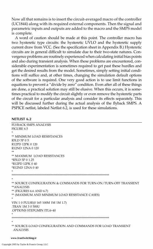
140
Practical Computer Analysis of Switch Mode Power Supplies
Now all that remains is to insert the circuit-averaged macro of the controller(UC1844) along with its required external components. Then the signal andparametric inputs and outputs are added to the macro and the SMPS modelis complete.
A word of caution should be made at this point. The controller macro hastwo hysteretic type circuits: the hysteretic UVLO and the hysteretic supplycurrent draw from VCC. (See the specification sheet in Appendix B.) Hystereticcircuits are in general difficult to simulate due to their two-state natures. Con-vergence problems are routinely experienced when calculating initial bias pointsand also during transient analysis. When these problems are encountered, con-siderable experimentation is sometimes required to get past these hurdles andget the desired results from the model. Sometimes, simply setting initial condi-tions will suffice and, at other times, changing the simulation default optionsof the software is required. One very good action is to use limit functions inequations to prevent a “divide by zero” condition. Even after all of these thingsare done, a practical solution may still be elusive. When this occurs, it is some-times practical to modify the circuit slightly or even remove the hysteretic partsof the circuit for a particular analysis and consider its effects separately. Thiswill be discussed further during the actual analysis of the flyback SMPS. APSPICE netlist, labeled Netlist 6.2, is used for these simulations.
NETLIST 6.2
FLYBACK SMPS ANALYSISFIGURE 6.5*** MINIMUM LOAD RESISTANCESR5LD 5P 0 5R12PD 12PK 0 120R12ND 12NA 0 120**** MAXIMUM LOAD RESISTANCES*R5LD 5P 0 1.25*R12PD 12PK 0 40*R12ND 12NA 0 40************************************************************************************* SOURCE CONFIGURATION & COMMANDS FOR TURN-ON/TURN-OFF TRANSIENT**ANALYSIS** (FIGURES 6.6 AND 6.7)** (MAXIMUM AND MINIMUM LOAD RESISTANCE CASES)*VIN 1 0 PULSE(0 165 100M 1M 1M 1.7).TRAN 1M 3 0 500U.OPTIONS STEPGMIN ITL4=40 ************************************************************************************* SOURCE-LOAD CONFIGURATION AND COMMANDS FOR LOAD TRANSIENT ANALYSIS
DK_1137.book Page 140 Wednesday, June 15, 2005 11:49 AM
Copyright 2005 by Taylor & Francis Group, LLC
www.IranSwitching.ir

Analyzing the Advanced SMPS Model
141
** (FIGURE 6.8)** (LOAD RESISTANCES SET TO MINIMUM)**VIN 1 0 DC 165*I5_LOAD 5P 0 PULSE(0 4 1.5 10U 10U 100M)*I12POS_LOAD 12PK 0 PULSE(0 .2 1.7 10U 10U 100M)*.TRAN 1M 2 0 500U*.OPTIONS STEPGMIN ITL4=20*.NODESET V(VG)=100 V(V)=30************************************************************************************* SOURCE CONFIGURATION AND COMMANDS FOR LINE REGULATION ANALYSIS** (FIGURE 6.9)** (MINIMUM AND MAXIMUM LOAD RESISTANCE CASES)**VIN 1 0 PWL (0,0) (100M,0) (101M,134) (2.5,133) (2.501,184) (2.700,184) (2.701,133) (3.0 134)*.TRAN 1M 3 0 500U*.OPTIONS STEPGMIN ITL4=40************************************************************************************* SOURCE-LOAD CONFIGURATION AND COMMANDS FOR CURRENT LIMITING** PERFORMANCE** (FIGURE 6.10)** (LOAD RESISTANCES SET TO MAXIMUM)**VIN 1 0 PULSE(0 165 100M 1M)*D_LOADSHORT 5P WW D1*V_LOADSHORT WW 0 PULSE(7 0 1.8 1M)*.TRAN 1M 4 0 200U*.OPTIONS STEPGMIN ITL4=20************************************************************************************* SOURCE CONFIGURATION AND COMMANDS FOR AC STABILITY ANALYSIS** (FIGURE 6.11)** (MAXIMUM AND MINIMUM LOAD RESISTANCE CASES)** (ACTIVATE VOVRD IN UVLO SECTION OF THE UC1844 SUBCKT)**VIN_MIN 1 0 DC 134 *VIN_MAX 1 0 DC 184*VACLG FBKI FBK AC 1VACLG FBKI FBK AC 0*.AC DEC 50 10 .1MEG*.OPTIONS STEPGMIN RELTOL=.004************************************************************************************ SOURCE CONFIGURATION AND COMMANDS FOR AC LINE REJECTION ANALYSIS** (FIGURE 6.12)** (MAXIMUM AND MINIMUM LOAD RESISTANCE CASES)** (ACTIVATE VOVRD IN UVLO SECTION OF THE UC1844 SUBCKT)**VIN_MIN 1 0 DC 134 AC 1*VIN_MAX 1 0 DC 184 AC 1
DK_1137.book Page 141 Wednesday, June 15, 2005 11:49 AM
Copyright 2005 by Taylor & Francis Group, LLC
www.IranSwitching.ir

142
Practical Computer Analysis of Switch Mode Power Supplies
*.AC DEC 50 10 100K*.OPTIONS STEPGMIN *************************************************************************************INPUT FILTERC1 VG 0 2.5UR1 1 VG 5***STARTUP RESISTORR2 VG FBK 56K**CONTROL CIRCUIT COMPONENTSR3 11 FBKI 20KR4 11 0 4.7KR5 COMP 11 150KC14 COMP 11 100PEFB 6A 6 V 0 .222VMFB 0 6FFB V 0 VMFB .222D1 6A 7 DC4 7 8 47UR9 7 0 68RC4 8 0 .4D2 7 FBK D.MODEL D D C3 FBK 0 .22UC2 FBK 9 100URC2 9 0 .2X1 FBK REF 11 COMP ISENSE 0 VG d 0 UC1844**5 VOLT OUTPUT STAGEVM5 3 0E5 V 3 2 0 11.25F5 0 2 VM5 11.25D5P 2 2K D1N5830C10 2K 0 4700UL5 2K 5PL 26URL5 5PL 5P 5MC11 5P 0 4700URCONV V 0 1E12**+12 VOLT OUTPUT STAGEE12P 12P 4 V 0 .2F12P V 0 VM12P .2VM12P 0 4D12P 12P 12PK D1N5806/27CC12 12PK 0 2200U**-12 VOLT OUTPUT STAGEE12N 5 12N V 0 .2F12N V 0 VM12N .2VM12N 5 0D12N 12NA 12N D1N5806/27CC13 12NA 0 2200U
DK_1137.book Page 142 Wednesday, June 15, 2005 11:49 AM
Copyright 2005 by Taylor & Francis Group, LLC
www.IranSwitching.ir

Analyzing the Advanced SMPS Model
143
*************************************************************************************UC 1844 PWM CONTROLLER CIRCUIT AVERAGING MACRO.SUBCKT UC1844 VCC 3 4 COMP 6 7 8 9 GND* VCC VREF VFB COMP ISENSE V VG d GND**NOTE: ALL SIGNAL INPUTS MUST BE REFERENCED TO THE UC1844 GND XUVLO VCC UVLO GND UVLOXREF UVLO VCC 3 VREF/2 GND REFXERRAMP 4 VREF/2 VCC COMP GND ERRAMPXDRC COMP 9 6 7A 8A UVLO GND DRC**DEPENDENT GENERATORS FOR GROUND ISOLATION IF DESIREDEVG 8A 0 8 GND 1EV 7A 0 7 GND 1.ENDS UC1844*.SUBCKT DRC 1 d 8 9 10 14 GND* COMP d ISENSE V VG UVLO GNDVBK 1 1A DC 2 R1 1A C 200KR2 C GND 100KX1 C 3 DIDEALX2 GND C DIDEALVLIM 3 GND DC 1RCONV1 6 0 1GRCONV2 7 0 1GRCONV3 4 0 1G*REL 10 9 1E8GL 0 11 10 9 1D1L 11 12 DXD2L 0 11 DXRLMIN 12 13 1VLMIN 13 0 1U*DX1 4 0 DXDX2 7 4 DXDX3 6 7 DX***IDRMAX VALUE = MAX LIMITED DUTY RATIOIDRMAX 7 6 DC .48DX4 0 6 DXDX5 6 6A DXVMD 6A 0EMD d 0 VALUE = I(VMD)*V(14)+1PRMD d 0 1.MODEL DX D IS=1E-12**L = 500U*RF = 0.55*TS = 25U*MC = 0***GCM 4 7 VALUE = (V(C)-RF*V(8))/((TS*RF)/(2*L))*(2*MC*L+V(12)))GCM 4 7 VALUE = LIMIT((V(C)-0.55*V(8))/((25U*0.55)/(2*500U)*(2*0*500U+V(12))),0,1)
DK_1137.book Page 143 Wednesday, June 15, 2005 11:49 AM
Copyright 2005 by Taylor & Francis Group, LLC
www.IranSwitching.ir

144
Practical Computer Analysis of Switch Mode Power Supplies
***GDCM 0 4 VALUE = V(C)/((TS*RF/L)*(MC*L+V(12))GDCM 0 4 VALUE = LIMIT(V(C)/((25U*0.55/500U)*(0*500U+V(12))),0,1)*.ENDS DRC*.SUBCKT UVLO VCC UVLO GND* VCC UVLO GNDRIN VCC 2 1KISUP 2 GND 1MXSUP GND 2 DIDEALG5 VCC GND VALUE = .01*V(UVLO,GND)** G1 AND G2 SET SET
UVLO START AND STOP LEVELS RESPECTIVELYG1 0 3 TABLE V(VCC,GND) = (0,0) (17,0) (18,20)G2 3 0 TABLE V(VCC,GND) = (9,20) (10,0) (17,0)CG2 3 0 20NR1 3 0 1E3G3 0 4 3 0 1G3HYST 0 4 VALUE = -100U+200U*V(UVLO,GND)CHOLD 4 0 20NG4 GND UVLO 4 GND 1**VOVRD TO BE INSERTED FOR UVLO OVERRIDE*VOVRD UVLO GND DC 1RG4 UVLO GND 1CG4 UVLO GND 1NX5 GND UVLO DIDEALX1 3 5 DIDEALX2 6 3 DIDEALX3 4 5 DIDEALX4 6 4 DIDEALVP 5 0 DC 1VN 0 6 DC 1.ENDS UVLO**5.0 VOLT REFERENCE MACRO.SUBCKT REF UVLO VCC VREF VREF/2 GND* UVLO VCC VREF VREF/2 GND* EIN 2 3 VCC GND .46E-3RVT 3 4 .32 TC=0.2E-3IVT GND 3 DC 3.125 VT GND 4 DC 1V5 1 2 DC 4.99342FUVLO 1 GND VMR 1EUVLO VREF 9 VALUE = V(1,GND)*V(UVLO,GND)VMR GND 9EVREF/2 VREF/2 GND VREF GND .5.ENDS REF**ERROR AMP MACRO.SUBCKT ERRAMP 6 7 8 1 GND * VIN VIP VCC OUTPUT GNDRIN 5 7 1MEGEPSRR 6 5 VALUE = (V(8)-15)*3E-4IBIAS GND 5 .3U
DK_1137.book Page 144 Wednesday, June 15, 2005 11:49 AM
Copyright 2005 by Taylor & Francis Group, LLC
www.IranSwitching.ir

Analyzing the Advanced SMPS Model
145
GA GND 2 7 5 1KRG 2 GND 30CG 2 GND 0.159MVNC 4 GND DC 1DN 4 2 D1VPC 3 GND DC 5DP 2 3 D1RO 1 2 3KRPS 8 0 1E8.ENDS ERRAMP.MODEL D1 D IS=1E-9 **X2 vg 0 d ISENSE 0 V 0 FLYBACK***********************************************************************************FLYBACK CONVERTER MODEL.SUBCKT FLYBACK vg GNDP d IL_P IL_N v GNDS * (VIN) (PRI GND) (DUTY RATIO) (INDUCTOR CURRENT) (VOUT) (SEC GND)*TS = 25U*L = 500U* **GLOD 9 8 VALUE = V(d)**2*(V(vg)**2/V(v))*(TS/(2*L))GLOD 9 8 VALUE = V(d)**2*(V(vg)**2/V(v))*(25U/(2*500U))***GLID CDMODE 1 VALUE = V(d)**2*V(vg)*(TS/(2*L))GLID CDMODE 1 VALUE = V(d)**2*V(vg)*(25U/(2*500U))***GLD 5 6 VALUE = V(d)**2*(V(vg)*(1+V(vg)/V(v))*(TS/(2*L))GLD 5 6 VALUE = V(d)**2*V(vg)*(1+(V(vg)/V(v)))*(25U/(2*500U))*F2 GNDP vg VM2 1VM2 1 0 DC 6D1 CDMODE 1 D2D2 0 CDMODE D2G1 0 CDMODE VALUE = V(d)*I(VM1)E2 4 3 VALUE = V(d)*V(vg)VM1 0 3L 4 5 500UXD5 5 6 DIDEALVM3 7 0E3 6 7 VALUE = (1-V(d))*V(v)G3 0 9 VALUE = (1-V(d))*I(VM3)D4 9 8 D2D5 0 9 D2.MODEL D2 D IS=1E-7 CJO=1NVM4 8 0 DC 6F4 GNDS V VM4 1*RISEN IL_P IL_N 1FISEN IL_N IL_P VM1 1*.ENDS FLYBACK**********************************************************************************
DK_1137.book Page 145 Wednesday, June 15, 2005 11:49 AM
Copyright 2005 by Taylor & Francis Group, LLC
www.IranSwitching.ir

146
Practical Computer Analysis of Switch Mode Power Supplies
**.SUBCKT DIDEALA 1 2EID 3 1 TABLE V(3,2) = (-1,1U) (1u,1U) (1,1)DIO 3 2 D.MODEL D D IS=1E-12 CC 1 2 10p.ENDS DIDEALA *.SUBCKT DIDEAL 1 2VAS 1 3 DC -1uD1 3 2 DD2 3 4 DD3 4 2 D1FAS 4 2 VAS 1.MODEL D D IS=1E-6 EG=0 XTI=-4 .MODEL D1 D EG=0 XTI=0 CC 1 2 .1P.ENDS DIDEAL*.LIB DIODE.LIB.PROBE.END
6.2.2 Flyback SMPS Large Signal Power ON/OFF Analysis
Begin by conducting a large signal analysis of the SMPS. First, simplyperform a turn-on and turn-off operation and investigate the various sig-nals that occur. Set the loads to their minimum values of 5
Ω
(1.0 amp) onthe +5-Vdc output and 120
Ω
(0.1 amp) on each of the
±
12-Vdc outputs.Figure 6.6a through Figure 6.6c show some of the waveforms. A 0 to 165 Vstep is applied for turn-on and after that cycle settles out, the power supplyis turned off by stepping the input voltage from 165 to 0 V. Figure 6.6ashows some results of this analysis.
After the 165-V input step voltage is applied, the VCC begins to rise.When the upper trip point of the UVLO is reached at VCC = 17 V, the UVLOsignal goes from 0 to 1, thus allowing the controller
X
1 (UC1844) to comealive. At this point, the operating supply current of
X
1 loads VCC so thatits voltage starts dropping, but eventually the rising bootstrap feedbackfrom node V(7) catches it. The control loop then begins to regulate holdingVCC at approximately 13.1 V. When the input voltage is suddenly reducedfrom 165 to 0 V for a normal turn-off, it is noted that the VCC begins todecrease with the converter duty ratio,
d
, rising to its maximum value of0.48. The UVLO drops to 0 when VCC is reduced to its lower trip point of10 V. The controller,
X
1, now shuts down by setting the converter duty ratio,
d
, to 0; all voltages continue to drop.Figure 6.6b shows more waveforms indicating how the circuit is performing.
Figure 6.6c provides a signal description of node CDMODE. This is a signal
DK_1137.book Page 146 Wednesday, June 15, 2005 11:49 AM
Copyright 2005 by Taylor & Francis Group, LLC
www.IranSwitching.ir

Analyzing the Advanced SMPS Model
147
FIGURE 6.6
(a) Flyback SMPS turn ON/OFF waveforms (minimum loads). (b) More flyback SMPS turnON/OFF waveforms (minimum loads).
200 VVin = 165 Vdc (Rectified 116 Vac)
Bootstrapped VCC (Feedback)VCC (UC1844)
V(1)
V(FBK)
V(X1.UVLO)
Converter Duty Ratio “d”UVLO
V(d)
V(7) V(5P)
150 V100 V
50 V
20 V15 V10 V
0 V
SEL>
>
1.0 V
0.5 V
0 V0 s 0.5 s 1.0 s 1.5 s
Time(a)
2.0 s 2.5 s 3.0 s
0 V
5 Vdc Output
200 V
V(1)
V(5P)
V(COMP)
V(12PK) V(12NA)
+12 Vdc Output5 Vdc Output
Vin = 165 Vdc (Rectified 116 Vac)
−12 Vdc Output
150 V100 V
50 V
15 V10 V
5 V0 V
−5 V−10 V−15 V
SEL>
>
2.5 V
5.0 V
0 V0 s 0.5 s 1.0 s 1.5 s
Time(b)
2.0 s 2.5 s 3.0 s
0 V
COMP (Voltage ErrorAmp Output)
DK_1137.book Page 147 Wednesday, June 15, 2005 11:49 AM
Copyright 2005 by Taylor & Francis Group, LLC
www.IranSwitching.ir

148
Practical Computer Analysis of Switch Mode Power Supplies
that indicates if the converter is in the continuous or the discontinuous mode.When its magnitude is 6 V, the converter is in the continuous mode and whenit is less than about a forward diode voltage drop (0.6 V) below ground, it isin the discontinuous conduction mode. Other voltage levels may occur in thiswaveform when no inductor current is flowing in the converter. The CDMODEnode is essentially floating under this condition and no significance should begiven to this signal for this zero inductor current condition.
The preceding ON/OFF analysis is now repeated with the maximum loadson the power supply. The 5-V load will now be set for 4 amps (1.2
Ω
) andeach of the
±
12-Vdc loads will be set at 0.3 amps (40
Ω
). The results areshown in Figure 6.7a through Figure 6.7c. An examination of the resultsreveals that, when powered, the COMP voltage is very near its maximumvalue of 5.0 V for this maximum load case. The converter is still operatingin the discontinuous mode, however. It only seems to go continuous for abrief period at the thresholds of regulation. If the load is increased further,current limiting will take place. This will be shown in the next section whena load sweep analysis is performed.
6.2.3 Flyback SMPS Large Signal Load and Line Transient Analysis
Now some transient load and line tests are performed on the three modelsand the effects considered. As a point of departure, first add load resistorsto the
+
5- and
±
12-Vdc outputs that represent minimum loading on thesupply. That would be 5
Ω
(1.0 amp) for the
+
5-Vdc output and 120
Ω
(0.1amp) for each of the
±
12-Vdc outputs. Then apply a pulse load to the
+
5 Vdc
FIGURE 6.6c
Still more flyback SMPS turn ON/OFF waveforms (minimum loads).
200 V
V(1)
V(FBK)
V(X2.CDMODE) V(X1.UVLO)
UVLO
CDMODE(Continuous Conduction Mode = 6 Volts)
(Discontinuous Conduction Mode = −0.6 Volts)
V(7) V(5P)
5 Vdc Output
VCC (UC1844)
Vin = 165 Vdc (Rectified 116 Vac)
Bootstrapped VCC (Feedback)
150 V100 V
50 V
20 V15 V10 V
0 V
SEL>
>
2.5 V5.0 V
0 V0 s 0.5 s 1.0 s 1.5 s
Time(c)
2.0 s 2.5 s 3.0 s
0 V
DK_1137.book Page 148 Wednesday, June 15, 2005 11:49 AM
Copyright 2005 by Taylor & Francis Group, LLC
www.IranSwitching.ir

Analyzing the Advanced SMPS Model
149
of an additional 4.0 amps and subsequently apply a 0.2 amp pulse load tothe
+
12-Vdc output; then look at the various circuit voltages. The inputvoltage is held constant at
+
165 Vdc (116 Vac). The results are shown inFigure 6.8a and Figure 6.8b. The results of Figure 6.8a show that the
+
5-V
FIGURE 6.7
(a) Flyback SMPS turn ON/OFF waveforms (maximum loads). (b) More flyback SMPS turnON/OFF waveforms (maximum loads).
200 V
V(1)
V(FBK)
V(X1.UVLO) V(d)
UVLO
Converter Duty Ratio “d”
V(7) V(5P)
5 Vdc Output
VCC (UC1844)
Vin = 165 Vdc (Rectified 116 Vac)
Bootstrapped VCC (Feedback)
150 V100 V
50 V
20 V15 V10 V
0 V
SEL>
>
0.5 V
1.0 V
0 V0 s 0.5 s 1.0 s 1.5 s
Time(a)
2.0 s 2.5 s 3.0 s
0 V
200 V
V(1)
V(5P)
V(COMP)
COMP (Voltage ErrorAmp Output)
V(12PK) V(12NA)
+12 Vdc Output
−12 Vdc Output5 Vdc Output
Vin = 165 Vdc (Rectified 116 Vac)150 V100 V
50 V
15 V10 V
5 V0 V
−5 V−15 V
SEL>
>
5.0 V
2.5 V
0 V0 s 0.5 s 1.0 s 1.5 s
Time(b)
2.0 s 2.5 s 3.0 s
0 V
DK_1137.book Page 149 Wednesday, June 15, 2005 11:49 AM
Copyright 2005 by Taylor & Francis Group, LLC
www.IranSwitching.ir

150
Practical Computer Analysis of Switch Mode Power Supplies
FIGURE 6.7c
Still more flyback SMPS TURN ON/OFF waveforms (maximum loads).
FIGURE 6.8a
Flyback SMPS load transient analysis (5-V load pulse).
200 V
V(1)
V(FBK)
V(X2.CDMODE) V(X1.UVLO)
UVLO
CDMODE(Continuous Conduction Mode = 6 Volts)(Discontinuous Conduction Mode = 0.6 Volts)
V(7) V(5P)5 Vdc Output
VCC (UC1844)
Vin = 165 Vdc (Rectified 116 Vac)
Bootstrapped VCC (Feedback)
150 V100 V
50 V
20 V15 V10 V
0 V
SEL>
>
2.5 V5.0 V
0 V0 s 0.5 s 1.0 s 1.5 s
Time(c)
2.0 s 2.5 s 3.0 s
0 V
1.45 s 1.50 sl(R5LD) + l(l5_LOAD)
1.55 sTime
(a)
+12 Vdc Transient
+5 Vdc Output Pulse Load (4 Amps)
−5 Vdc Transient
1.60 s 1.65 s
6.0 V5.8 V5.6 V5.4 V5.2 V5.0 V
13.0 V
V(5P)
V(12PK)
12.8 V12.6 V12.4 V12.2 V12.0 V
6.0 A4.0 A
0 A
SEL>
>
DK_1137.book Page 150 Wednesday, June 15, 2005 11:49 AM
Copyright 2005 by Taylor & Francis Group, LLC
www.IranSwitching.ir
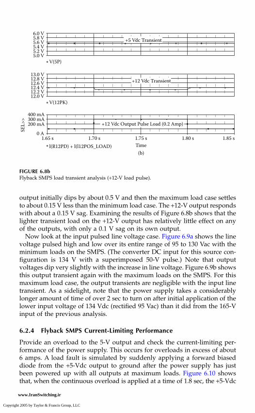
Analyzing the Advanced SMPS Model
151
output initially dips by about 0.5 V and then the maximum load case settlesto about 0.15 V less than the minimum load case. The
+
12-V output respondswith about a 0.15 V sag. Examining the results of Figure 6.8b shows that thelighter transient load on the
+
12-V output has relatively little effect on anyof the outputs, with only a 0.1 V sag on its own output.
Now look at the input pulsed line voltage case. Figure 6.9a shows the linevoltage pulsed high and low over its entire range of 95 to 130 Vac with theminimum loads on the SMPS. (The converter DC input for this source con-figuration is 134 V with a superimposed 50-V pulse.) Note that outputvoltages dip very slightly with the increase in line voltage. Figure 6.9b showsthis output transient again with the maximum loads on the SMPS. For thismaximum load case, the output transients are negligible with the input linetransient. As a sidelight, note that the power supply takes a considerablylonger amount of time of over 2 sec to turn on after initial application of thelower input voltage of 134 Vdc (rectified 95 Vac) than it did from the 165-Vinput of the previous analysis.
6.2.4 Flyback SMPS Current-Limiting Performance
Provide an overload to the 5-V output and check the current-limiting per-formance of the power supply. This occurs for overloads in excess of about6 amps. A load fault is simulated by suddenly applying a forward biaseddiode from the
+
5-Vdc output to ground after the power supply has justbeen powered up with all outputs at maximum loads. Figure 6.10 showsthat, when the continuous overload is applied at a time of 1.8 sec, the
+
5-Vdc
FIGURE 6.8b
Flyback SMPS load transient analysis (
+
12-V load pulse).
1.65 s 1.70 sl(R12PD) + l(l12POS_LOAD)
1.75 sTime
(b)
+12 Vdc Transient
+12 Vdc Output Pulse Load (0.2 Amp)
+5 Vdc Transient
1.80 s 1.85 s
6.0 V5.8 V5.6 V5.4 V5.2 V5.0 V
13.0 V
V(5P)
V(12PK)
12.8 V12.6 V12.4 V12.2 V12.0 V
400 mA300 mA200 mA
0 ASEL>
>
DK_1137.book Page 151 Wednesday, June 15, 2005 11:49 AM
Copyright 2005 by Taylor & Francis Group, LLC
www.IranSwitching.ir

152
Practical Computer Analysis of Switch Mode Power Supplies
output voltage immediately drops to about that of a forward biased diode(approximately 0.6 V). The bootstrap feedback voltage also drops but the+12-V output decays more slowly. The VCC voltage eventually drops tobelow its lower UVLO trip point of 10 V and the converter is switched off.The UC1844 controller supply current drops and the VCC voltage starts torise again. When it reaches its upper UVLO trip level of 17 V, the converterattempts to start up again. With the overload still applied to the 5-V output,
(a)
FIGURE 6.9(a) Flyback SMPS line transient analysis (minimum load case). (b) Flyback SMPS line transientanalysis (maximum load case).
Time0 s 0.5 s 1.0 s 1.5 s 2.0 s 2.5 s 3.0 s1 V(5P) V(12PK)
5.540 V5.545 V5.550 V5.555 V5.560 V1
12.35 V
12.37 V12.38 V12.39 V2
SEL>> +5 Vdc Output Transient
+12 Vdc Output TransientV(FBK) V(7) V(5P)
0 V5 V
10 V15 V20 V
Bootstrapped VCC (Feedback)VCC (UC1844)
+5 Vdc Output
V(1)0 V
100 V
200 V Vin = 134 Vdc (Rectified 95 Vac)
Transient Vin = 50 Volt Pulse (Rectified 95 Vac to 134 Vac)
2
Time(b)
0 s 0.5s 1.0 s 1.5 s 2.0 s 2.5 s 3.0 s1 V(5P) V(12PK)
5.395 V5.400 V5.405 V5.410 V5.415 V1
12.10 V
12.12 V12.13 V12.14 V2
SEL>
>
+5 Vdc Output+12 Vdc Output
V(FBK) V(7) V(5P)0 V5 V
10 V15 V20 V
Bootstrapped VCC (Feedback)VCC (UC1844)
+5 Vdc Output
V(1)0 V
100 V
200 V Vin = 134 Vdc (Rectified 95 Vac)
Transient Vin = 50 Volt Pulse (Rectified 95 Vac to 134 Vac)
2
DK_1137.book Page 152 Wednesday, June 15, 2005 11:49 AM
Copyright 2005 by Taylor & Francis Group, LLC
www.IranSwitching.ir

Analyzing the Advanced SMPS Model 153
the previously described shutdown starts over again, thus starting a steadystate limit cycle as shown in Figure 6.10.
6.2.5 Flyback SMPS AC Stability Analysis
The AC stability of the example flyback switching power supply will beexamined now. The AC loop gain phase plots for the four conditions ofmaximum and minimum line and load will be discussed. Figure 6.11athrough Figure 6.11d show the results. The stability margins are very good,with phase margins all in excess of 90°. The unity gain crossover is noted tobe fairly independent of line voltage variations but does decrease from 300Hz at minimum loads to 100 Hz at maximum loads.
6.2.6 Flyback SMPS AC Line Rejection Analysis
The AC line noise rejection characteristics of the flyback SMPS are nowexamined. This is an important part of any power supply analysis whenpower line noise is expected or when a stringent audio susceptibility spec-ification is required to be met. An AC voltage is injected onto the input powerlines and the frequency is swept over the range of 10 to 100 kHz. The resultsfor the four extremes of maximum and minimum load current and linevoltage are shown in Figure 6.12a through Figure 6.12d. The rejection is over80 dB for all conditions and does not vary significantly over the ranges. Thisis characteristic of the discontinuous conduction mode in general.
FIGURE 6.10Flyback SMPS current limiting performance.
Time0 s 0.5 s 1.0 s 1.5 s 2.0 s 2.5 s 3.0 s 3.5 s 4.0 s
1 V(5P) V(12PK)
0 V2.0 V4.0 V6.0 V1 18 V
12 V
0 V
2
SEL>
> +5 Vdc Output+12 Vdc Output
+5 Vdc Output
V(FBK) V(7) V(5P)0 V
15 V10 V
5 V
20 V25 V Bootstrapped VCC (Feedback)
Overload Applied at this Time
VCC (UC1844)
V(1)0 V
100 V
200 VVin = 165 Vdc (Rectified 116 Vac)
2
DK_1137.book Page 153 Wednesday, June 15, 2005 11:49 AM
Copyright 2005 by Taylor & Francis Group, LLC
www.IranSwitching.ir

154 Practical Computer Analysis of Switch Mode Power Supplies
FIGURE 6.11a and 6.11b(a) Flyback SMPS AC loop gain analysis (minimum line, minimum loads). (b) Flyback SMPSAC loop gain analysis (maximum line, minimum loads).
Frequency
(a)
10 Hz 100 Hz 1.0 KHz 10 KHz 100 KHzDB(V(FBK))–DB(V(FBKI))
−40
−20
0
20
40
SEL>
> Loop GainMinimum Vin 134 Vdc (Rectified 95 Vac)Minimum Loads
P(V(FBK))–P(V(FBKI))0 d
20 d40 d60 d80 d
100 d120 d140 d160 d180 d
Loop Phase
Frequency
(b)
10 Hz 100 Hz 1.0 KHz 10 KHz 100 KHzDB(V(FBK))–DB(V(FBKI))
−40
−20
0
20
40
SEL>
> Loop Gain
Maximum Vin 184 Vdc (Rectified 130 Vac)Minimum Loads
P(V(FBK))–P(V(FBKI))0 d
20 d40 d60 d80 d
100 d120 d140 d160 d180 d
Loop Phase
DK_1137.book Page 154 Wednesday, June 15, 2005 11:49 AM
Copyright 2005 by Taylor & Francis Group, LLC
www.IranSwitching.ir

Analyzing the Advanced SMPS Model 155
FIGURE 6.11c and 6.11d(c) Flyback SMPS AC loop gain analysis (maximum line, maximum loads). (d) Flyback SMPSAC loop gain analysis (minimum line, maximum loads).
Frequency(c)
10 Hz 100 Hz 1.0 KHz 10 KHz 100 KHzDB(V(FBK))–DB(V(FBKI))
−40
−20
0
20
40
SEL>
> Loop Gain
Maximum Vin 184 Vdc (Rectified 130 Vac)Maximum Loads
P(V(FBK))–P(V(FBKI))0 d
20 d40 d60 d80 d
100 d120 d140 d160 d180 d
Loop Phase
Frequency(d)
10 Hz 100 Hz 1.0 KHz 10 KHz 100 KHzDB(V(FBK))–DB(V(FBKI))
−40
−20
0
20
40
SEL>
> Loop Gain
Minimum Vin 134 Vdc (Rectified 95 Vac)Maximum Loads
P(V(FBK))–P(V(FBKI))0 d
20 d40 d60 d80 d
100 d120 d140 d160 d180 d
Loop Phase
DK_1137.book Page 155 Wednesday, June 15, 2005 11:49 AM
Copyright 2005 by Taylor & Francis Group, LLC
www.IranSwitching.ir

156 Practical Computer Analysis of Switch Mode Power Supplies
FIGURE 6.12a and 6.12b(a) Flyback SMPS AC line rejection analysis (minimum line, minimum loads). (b) Flyback SMPSAC line rejection analysis (maximum line, minimum loads).
Frequency(a)
10 Hz 100 Hz 1.0 KHz 10 KHz 100 KHzDB(V(5P))
−200
−180
−160
−140
−120
−100
−80
−60
−40
−20
0
Minimum LoadsMinimum Vin 134 Vdc (Rectified 95 Vac)
Frequency(b)
10 Hz 100 Hz 1.0 KHz 10 KHz 100 KHzDB(V(5P))
−200
−180
−160
−140
−120
−100
−80
−60
−40
−20
0
Minimum LoadsMaximum Vin 184 Vdc (Rectified 130 Vac)
DK_1137.book Page 156 Wednesday, June 15, 2005 11:49 AM
Copyright 2005 by Taylor & Francis Group, LLC
www.IranSwitching.ir

Analyzing the Advanced SMPS Model 157
6.3 Practical Buck SMPS Analysis with Parasitic Resistances
Consider another example, which will show a buck topology switch modeconverter when parasitic resistances are considered. Modern computerpower supplies using low power supply output voltages and relatively large
FIGURE 6.12c and 6.12d(c) Flyback SMPS AC line rejection analysis (maximum line, maximum loads). (d) Flyback SMPSAC line rejection analysis (minimum line, maximum loads).
Frequency(c)
10 Hz 100 Hz 1.0 KHz 10 KHz 100 KHzDB(V(5P))
−200
−180
−160
−140
−120
−100
−80
−60
−40
−20
0
Maximum LoadsMaximum Vin 184 Vdc (Rectified 130 Vac)
Frequency(d)
10 Hz 100 Hz 1.0 KHz 10 KHz 100 KHzDB(V(5P))
−200
−180
−160
−140
−120
−100
−80
−60
−40
−20
0
Maximum LoadsMinimum Vin 134 Vdc (Rectified 95 Vac)
DK_1137.book Page 157 Wednesday, June 15, 2005 11:49 AM
Copyright 2005 by Taylor & Francis Group, LLC
www.IranSwitching.ir

158 Practical Computer Analysis of Switch Mode Power Supplies
load currents pose some unique design challenges in achieving high powerconversion efficiencies. The example presented here illustrates how parasiticeffects that may have previously been considered second and third order arenow significant and need to be considered in the analysis. An equivalentcircuit for the converter, which can be used for analyzing the effects of theseparasitic effects, will now be developed.
6.3.1 Practical Buck Converter Model Developmentwith Parasitic Resistances
Figure 6.13 shows the schematic diagram of the general example. It utilizessynchronous rectification when converting the input voltage to a PWMpulsed DC voltage. This implies that the power converter is always operatingin the continuous conduction mode and that the macromodel only needs tobe capable of emulating that condition. The power supply has a relativelylow output voltage of 1.8 V and a relatively high output current of 50 amps.With an input voltage of 5 to 28 V, conduction voltage drops will be signif-icant and a valid accounting of these is deemed necessary. Figure 6.14 showsthe large signal circuit-averaged model of the converter section. The devel-opment of this model is explained next.
When Figure 6.14 is first examined, one of the very noticeable things isthe considerable number (six) of series resistances elements in the model.All of these component resistances are undesirable because they decreasethe efficiency of the power conversion process. Dr. Middlebrook’s paper20
provides the basis for determining the series resistance effects of elementsthat are functions of the converter duty ratio, d. These resistances can bequantified as follows:
• RSENSE. This is the only one of the series resistances that is not con-sidered an inherent “parasitic” resistance because it was intentionallyinserted for the purpose of measuring current. Unfortunately, however,
FIGURE 6.13Buck converter with synchronous rectification.
VIN
5 - 28 Vdc
+
-
Q1
RLOAD
CO
VOUT = 1.8 V
d
LI
CI
LO
RSENSE
d'0.036 Ω
+ -ISENSE
DK_1137.book Page 158 Wednesday, June 15, 2005 11:49 AM
Copyright 2005 by Taylor & Francis Group, LLC
www.IranSwitching.ir

Analyzing the Advanced SMPS Model 159
its effects on efficiency are still negative and should be considered. Asthe current in this resistance is equal to the inductor current and is not“chopped” by the power switches, its equivalent value is consideredto be equal to its actual value for analysis purposes. On the other hand,if the inductor current has a significantly large ripple content, a dutyratio-dependent value of this resistance might be in order.
• RLO. This resistance is the series resistance of the averaging inductor,LO, and is in series with the sense resistor, RSENSE. Its circuit effectsare the same as those of RSENSE. This resistance is in general afunction of temperature and frequency. Once the temperature of thedevice has been determined, the winding resistance can be adjustedby the resistance temperature coefficient, RTC, of the coil windingmaterial. (Most windings will be copper with an RTC of nominally+0.4%/°C.) Frequency dependency is determined by skin and prox-imity effects; however, for most power supply inductor designs, theAC ripple current is reduced by the inductor and these AC effectsare not relevant. (When considering the effects of transformer windings,however, when the current is chopped and thus produces a considerableamount of AC current, the AC winding resistances now assume a wholenew significance and generally must be considered.16,17) Equation 6.1shows how this resistance varies with temperature.
(6.1)
• RQ2e. This resistance is a function of the ON resistance, RDS(ON), ofMOSFET, Q2. The current through this device flows only during theinterval, d′, so its equivalent series effects are a function of the dutyratio. For MOSFET switching devices, this resistance is composed of
FIGURE 6.14Buck converter model with parasitic resistances.
+LO
RCO
RLOAD
COd
d
+
+
VM0 V
RSENSE
LI
RESR
CI
0.036 Ω
RLORQ2eRQ1e
RCIe
RLI
G
EVIN
VOUT
-
RLO R T CC= × + − °°25 1 004 25[( . ( )]
DK_1137.book Page 159 Wednesday, June 15, 2005 11:49 AM
Copyright 2005 by Taylor & Francis Group, LLC
www.IranSwitching.ir

160 Practical Computer Analysis of Switch Mode Power Supplies
the silicon channel resistance and has the RTC of silicon, which isnominally +0.7%/°C. The equivalent series value of RQ2e is therefore:
(6.2)
• RQ1e. This resistance is a function of the ON resistance, RDS(ON), ofMOSFET, Q1. Because the current through this device flows onlyduring the interval, d, its equivalent series effects are also a functionof the duty ratio. The equivalent series value of RQ1e is therefore:
(6.3)
• RCIe. This series resistance is a function of the equivalent seriesresistance, RESR, of the input filter capacitor, CI. RESR may some-times be a complex function of temperature, T, and frequency, F (seeSection 5.1.1). There are basically two components of AC currentsflowing in this capacitor: the high-frequency converter switchingfrequency component and the low-frequency components associatedwith the dynamical behavior of the power supply. The high-fre-quency component of AC current in this capacitor is also a functionof the converter duty ratio, d. Its series circuit resistance effect forthe buck topology is as expressed by RCIe in Equation 6.4. The valueof RCI is the value of RESR that exists at the switching frequency ofthe converter. (Although not proven here, this duty ratio modulatedresistance, RCIe, is valid for power loss calculations.) The value ofRESR is still maintained in series with capacitor, CI, when perform-ing AC and transient analyses on the power supply.
(6.4)
• RLI. This is the series resistance of the input filter inductor and is notconsidered to have any chopped current flowing in it. It is thereforesimply represented by the actual value of the low-frequency DC resis-tance, RLI, and expressed by:
(6.5)
When these parasitic resistances are modeled, the wiring or conductionpaths connecting these components have resistances and also must be insertedin the analysis model when deemed significant. The wiring resistances that
RQ e R T C dDS ON Q2 1 007 252= × + − ° × ′( ) [( . ( )]
RQ eR T C
dDS ON Q1
1 007 251=× + − °⎛
⎝⎜
⎞
⎠⎟
( ) [( . ( )]
RCIe RCIdd
f T F= × ′⎛⎝⎜
⎞⎠⎟
× ( , )
RLI R T CC= × + − °°25 1 004 25[( . ( )]
DK_1137.book Page 160 Wednesday, June 15, 2005 11:49 AM
Copyright 2005 by Taylor & Francis Group, LLC
www.IranSwitching.ir

Analyzing the Advanced SMPS Model 161
are in series with the component resistances as indicated earlier are simplyinserted in series with them and are treated with the same duty ratio mod-ulation effects.
The converter of Figure 6.14 may be analyzed at the converter level ormay simply be inserted into an appropriate control circuit to create thedesired SMPS. Then, the complete switching regulator can be analyzed forchanges of performance and efficiency by inserting, removing, or modify-ing these parasitic resistances as desired. These resistances may sometimeshave a positive effect on the low-frequency performance of a power supplybecause the added resistances tend to increase circuit damping of theresonant LC filter circuits. This may result in less ringing and overshootvoltages during transient operating conditions. This damping may alsohelp reduce high-frequency switching noise; however, in general, theseresistances are not sufficient and additional damping circuits are requiredto deal with this.
6.4 Practical “Loop-Opening” Techniques for AC Analysis
When a feedback control loop for an AC loop gain analysis is “opened,” apoint of accessibility must be selected. Figure 6.15 shows the general case inwhich a unity gain voltage amplifier with output source impedance, ZS,drives the input of voltage amplifier, A, whose input impedance is ZI. Forthis general case, it is easy to see that the actual loop gain, T, is simply:
(6.6a)
FIGURE 6.15General feedback circuit showing loop opening accessibility for AC stability analysis.
T A ZSZI
=+
⎛
⎝
⎜⎜⎜
⎞
⎠
⎟⎟⎟
1
1
ZI
ZS A1-+
Loop Gain = “T”
Loop OpeningAccessibility
Point
DK_1137.book Page 161 Wednesday, June 15, 2005 11:49 AM
Copyright 2005 by Taylor & Francis Group, LLC
www.IranSwitching.ir

162 Practical Computer Analysis of Switch Mode Power Supplies
Rearranging, T may also be expressed as:
(6.6b)
As a point of departure, open the loop and insert a floating test voltagesignal as shown in Figure 6.16a. It is important to note that the DC operatingbias points of the circuit have been preserved because the AC characteristicscould possibly be altered for different DC bias points in some circuits. Equation6.7 shows the equation for an apparent loop voltage gain, TV, expressed as aratio of the voltages vOUT and vIN:
(6.7)
FIGURE 6.16(a) General feedback circuit showing loop opening with floating voltage injected signal, vAC.(b) General feedback circuit showing loop opening with current-injected signal, iAC.
T AZZ
I
SZIZS
=⎛
⎝⎜⎞
⎠⎟ +
⎛
⎝⎜⎜
⎞
⎠⎟⎟
1
1
Tvv
AZZ
VOUT
IN
S
I= = +
ZI
ZI
ZS
ZS
A1
vINvOUT
+−+
Loop Gain = “T”
Loop Gain = “T”
+
+−
−
vAC
iOUT
iAC
iIN
1−+ A
(a)
(b)
DK_1137.book Page 162 Wednesday, June 15, 2005 11:49 AM
Copyright 2005 by Taylor & Francis Group, LLC
www.IranSwitching.ir

Analyzing the Advanced SMPS Model 163
Comparing Equation 6.6a and Equation 6.7, it is easily seen that, when ZS
is much less than ZI, the loop gain reduces to A for both cases. Therefore, theeasily obtained ratio, TV, is an accurate indication of the actual loop gain, T,which is in this case simply A.
Now take the case in which the only point of accessibility is where ZS isnot much less than ZI. It is now obvious that TV is not the actual gain T. Avery obvious thing to note is that, although the value of T now actuallydecreases with increasing values of ZS (or decreasing values of ZI), the valueof TV now increases, thereby giving a false impression that the gain is increas-ing when it is in reality decreasing. What is one to do now?
Apply the principal of circuit duality and examine the results obtainedwhen a test current signal is injected as shown in Figure 6.16b. This is donein an attempt to obtain a current loop gain expression and see how it com-pares to the equation for the actual loop gain, T. Equation 6.8 shows theequation for this apparent current loop gain, TI, expressed as a ratio of thecurrents iOUT and iIN:
(6.8)
By making the analogous comparison of Equation 6.6b and Equation 6.8,it is easily seen that when ZI is now much less than ZS, the loop gain reducesto for both cases. Therefore, the ratio, TI, is an accurate indication ofthe actual loop gain, T, which is in this case simply, . Unfortunately,in the case when ZI is not much less than ZS, the terms T and TI do notcompare favorably and it is obvious that TI is not the actual gain T.
By combining Equation 6.6a, Equation 6.7, and Equation 6.8, one can nowproduce an equation that does yield the actual loop gain as expressed inEquation 6.9:
(6.9)
The results obtained from performing and combining the results of the twoapparent gain tests — namely, TV and TI — now produce the true and actualloop gain T. Dr. Middlebrook has derived this equation in eloquent fashion.29
The facilitation of this equation will be discussed later in this section.As now might be surmised from Equation 6.6a and Equation 6.7 and the
preceding discussion, it is in all probability most desirable to open the loopand inject a stimulus voltage test signal at a point at which a very lowimpedance source drives a very high impedance load. This might be wherethe low output impedance of an opamp circuit drives a high input impedanceload as intimated in Figure 6.15. ZS is much less than ZI; thus, it is ensuredthat the measured feedback signal is produced solely by the loop gain ampli-fied test signal and that the signal does not have any components to whichany other factors attribute. All the examples presented in this book open the
Tii
AZZ
ZZI
OUT
IN
I
S
I
S
= = +
AZIZS
AZIZS
TT TT T
V I
V I
=+ +1
DK_1137.book Page 163 Wednesday, June 15, 2005 11:49 AM
Copyright 2005 by Taylor & Francis Group, LLC
www.IranSwitching.ir

164 Practical Computer Analysis of Switch Mode Power Supplies
loop and inject the AC test signal at points at which this condition is con-sidered met for the frequency ranges of interest.
Two loop opening methods have been used in the examples. One is withthe use of the ultralow-pass filter method shown in Figure 4.9 and Figure 4.23.With the values of LOL and COL extremely large, it is easy to see that theAC feedback is opened and the DC feedback is maintained with DC biaspoints remaining unchanged. This ensures that the correct DC operatingpoint is established for AC analysis. Also, the large value of LOL ensures avery high AC impedance to prevent any further possible loading of themeasured AC feedback signal. This setup allows for a practical computermeasurement of the actual loop gain, but obviously is impractical to imple-ment in an actual physical test setup due to the extremely large values ofLOL and COL. It is also easy to see that, when the impedance effects of ZS
and ZI modify the actual gain, T, as stated earlier, this method will not detectthis effect. It will only indicate the incorrect result and indicate a gain of A.
The second signal injection method is called the floating voltage injectionsignal method. This is the one illustrated in the general example of Figure 6.16aand yields the result of TV. It is also used in the example shown in Figure 6.5.Voltage source, VACLG, is a floating injected signal connected between nodesFBKI and FBK. In the example, it is easy to see that the impedance seen lookingback into node FBK is much lower than the impedance seen looking forwardinto node FBKI for the frequencies of interest.
To utilize Equation 6.9 in performing a practical computer AC loop gainanalysis, one might set up two circuit models that will each provide a tabula-tion of the desired gain and phase vs. frequency computations of Equation 6.7and Equation 6.8. The two sets of results are then combined in a spreadsheetprogram that uses Equation 6.9 to compute the actual values of T. The nowcomputed values of gain and phase vs. frequency of T can be plotted to createa Bode plot providing the desired AC loop gain characteristics.
Another method that might be used to obtain the actual loop gain T moredirectly and more conveniently than the spreadsheet approach is shown inFigure 6.17. This approach obtains the true gain T directly from the simula-tion by setting up two identical circuits that are each stimulated with iden-tical voltage amplitude and phase signals. A signal cancellation or “nulling”scheme is used in conjunction with a postsignal processor to determine theactual true loop gain, T, regardless of the impedance effects. The circuit inFigure 6.17a is simply an ultralow-pass filter opened loop and the measuredsignal, VOC, is simply the open circuit AC signal. With a unit input signalof VAC = 1, the value of VOC is simply:
VOC = A (6.10)
Now if the signal VOC from circuit a) is inserted as E1 in circuit b), the ACequivalent circuit current into which i1 flows is ZI and has zero open circuitvoltage source. This zero open circuit voltage is produced because E1 nowexactly cancels out the amplified voltage produced by gain, A, in circuit b),which is also equal to VOC. ZS and ZI now form a simple current divider for
DK_1137.book Page 164 Wednesday, June 15, 2005 11:49 AM
Copyright 2005 by Taylor & Francis Group, LLC
www.IranSwitching.ir

Analyzing the Advanced SMPS Model 165
current, i2, produced by the voltage source, VAC. (Keep in mind that capacitorsCOL and CLRGE are short circuits for AC signals, and LOL is an open circuitfor AC signals.) From the divider relationship, it can be shown that
(6.11)
FIGURE 6.17Analysis model for determining actual loop gain, T, using the null voltage method.
ZI
ZS A1-+
Loop Gain = “T”
VOC+
+-
“Ultra Low Pass Filter”
LOL
COL
VAC1
“Null”
ZI
ZS A1-+
Loop Gain = “T”
+
“Ultra Low Pass Filter”
LOL
COL
VAC1
CLRGE
+
“Null”
i1 i2
E11
(VOC)
b)
a)
ii ZS
ZI
1
2
1
1=
+
⎛
⎝⎜⎜
⎞
⎠⎟⎟
DK_1137.book Page 165 Wednesday, June 15, 2005 11:49 AM
Copyright 2005 by Taylor & Francis Group, LLC
www.IranSwitching.ir

166 Practical Computer Analysis of Switch Mode Power Supplies
Note that the easily obtained simulated quantities of Equation 6.10 and Equa-tion 6.11 now have each of the two required terms needed in Equation 6.6a todetermine the actual loop gain, T.
(6.12)
When Equation 6.10 and Equation 6.11 are routinely combined in apostsimulation processor equation, the desired gain in decibels and the phaseof T can easily be obtained:
dB(T) = dB(VOC) + dB(i1) – dB(i2) (6.13)
and
Phase(T) = Phase(VOC) + Phase(i1) – Phase(i2) (6.14)
This method is probably not the only configuration for determining actualloop gain T directly from a simulation and the reader is encouraged to exploreother possibilities.
6.5 Buck SMPS Soft Start and “Hiccup” Current Limit Analysis
Section 6.2 examined most of the pertinent performance characteristics of aflyback SMPS that uses a UC1844 PWM controller behavioral model. In thissection, some analysis will be performed on a very simple continuous modelarge signal buck converter model that uses the macromodel of the UC1825APWM controller developed in Appendix B. The UC1825A controller is a moresophisticated device than the UC1844, with such features as soft start controland pulse-by-pulse current limiting. It also contains a latched overcurrentcircuit, which facilitates a full soft restart of the power supply when anovercurrent condition is encountered. If the overcurrent persists, a hiccupon–off mode of operation is instituted. This section will demonstrate someof the performance characteristics that one might expect during turn ONand current-limiting situations when this controller is used.
Figure 6.18 shows a very basic SMPS using a simple continuous modelarge signal buck converter model and the UC1825A PWM controller mac-romodel developed in Appendix B. Netlist 6.3 shows the circuit details for
T A VOCiiZS
ZI
=+
⎛
⎝⎜⎜
⎞
⎠⎟⎟
= ( )⎛⎝⎜
⎞⎠⎟
1
11
2
DK_1137.book Page 166 Wednesday, June 15, 2005 11:49 AM
Copyright 2005 by Taylor & Francis Group, LLC
www.IranSwitching.ir

Analyzing the A
dvanced SMP
S Model
167FIGURE 6.18SMPS model using the UC1825A PWM controller circuit-averaged macromodel.
ERV F
CCVTUO A/E
NI V
GV
V
d
DNG
IN
IS ESNE7
d9
01
LFRSTCM
MILR
SS
V 31
11
21
8
SC S0. U10
IVF1
FR1 Ω
V“ ”G
AV C
1RK5.7
2R5.7 K
2CN1
3RK01
4RK01
5RK01
1X1CU A528
V“ ”G
V“ ”
V“ ”
OL05 U
OCR1
LR DAO
OCU002
d
d
+
+MV 1V 0
ILU01
CR I.0 1
ICU01
5 Ω
1G
1E
IV N
TUOV
+ 1OC01 U
VGV1
2 3
4
6
V“ ”G V“ ”
1CP01
5
DLVOG
ALCX PMLAEDID
d“ ”
DK
_1137.book Page 167 Wednesday, June 15, 2005 11:49 A
M
Copyright 2005 by T
aylor & Francis G
roup, LL
C
www.IranSwitching.ir

168 Practical Computer Analysis of Switch Mode Power Supplies
the analyses performed here. The model, by definition, is always in thecontinuous mode, which suggests that the converter would use synchronousrectification. Also, an AC loop gain and line voltage rejection analysis willbe conducted to demonstrate how the UN1825A macromodel needs to beset up for this type of analysis.
NETLIST 6.3
BUCK CONVERTER SOFT START AND LOAD SHORT ANALYSIS USING UC1825A PWM CONTROLLER
FIGURE 6.18**************************************************************************** SOURCE/LOAD CONFIGURATION & COMMANDS FOR TURN-ON/TURN-OFF ** TRANSIENT ANALYSIS** WITH SOFT START CAPACITOR (CSS) VALUES OF 0.01U, 0.1U, AND 0.001U** (FIGURE 6.18)*** (Figure 6.19)CSS SS 0 .01URLOAD V 0 5VIN 1 0 PULSE(0 30 1M .1M 1M 10M).TRAN 10U 14M 0 10U SKIPBP.OPTIONS RELTOL=.005 ITL4=60 PIVREL=1E-6*** (Figure 6.20)*CSS SS 0 .1U*RLOAD V 0 5*VIN 1 0 PULSE(0 30 1M .1M 1M 80M)*.TRAN 10U 100M 0 30U SKIPBP*.OPTIONS RELTOL=.005 ITL4=80 PIVREL=1E-6*** (Figure 6.21)*CSS SS 0 .001U*RLOAD V 0 5*VIN 1 0 PULSE(0 30 1M .1M 1M 2M)*.TRAN 10U 6M 0 5U SKIPBP*.OPTIONS RELTOL=.005 ITL4=60 PIVREL=1E-6********************************************************************************************** SOURCE/LOAD CONFIGURATION & COMMANDS FOR OUTPUT OVERLOAD & SHORT** CIRCUIT TRANSIENT ANALYSIS** WITH SOFT START CAPACITOR (CSS) VALUES OF 0.01U AND 0.1U** (FIGURE 6.18)**VIN 1 0 DC 20*ROVLD P 0 1*GOVLD V 0 VALUE = LIMIT(V(V)*V(P),0,20)*.OPTIONS RELTOL=.01 ITL4=60 PIVREL=1E-6 **CSS SS 0 .01U*RLOAD V 0 5
DK_1137.book Page 168 Wednesday, June 15, 2005 11:49 AM
Copyright 2005 by Taylor & Francis Group, LLC
www.IranSwitching.ir

Analyzing the Advanced SMPS Model 169
** (FIGURE 6.22) 2 OHM OVERLOAD*IOVLD 0 P PULSE(0 .5 10m .01m .01m 18m)** (FIGURE 6.23) 0.01 SHORT*IOVLD 0 P PULSE(0 100 10m .01m .01m 18m)*.TRAN 10U 40M 0 20U SKIPBP**CSS SS 0 .1U*RLOAD V 0 5** (FIGURE 6.24) 2 OHM OVERLOAD*IOVLD 0 P PULSE(0 .5 80m .01m .01m 50m)** (FIGURE 6.25) 0.01 SHORT*IOVLD 0 P PULSE(0 100 80m .01m .01m 50m)*.TRAN 10U 200M 0 50U SKIPBP********************************************************************************************** SOURCE/LOAD CONFIGURATION & COMMANDS FOR LOAD SHORT AT TURN-ON/** TURN-OFF TRANSIENT ANALYSIS** WITH SOFT START CAPACITOR (CSS) VALUES OF 0.01U, 0.1U AND 0.001U** (FIGURE 6.18)*** (Figure 6.26)*CSS SS 0 .01U*RLOAD V 0 .01*VIN 1 0 PULSE(0 30 1M .1M 1M 10M)*.TRAN 10U 14M 0 10U SKIPBP*.OPTIONS RELTOL=.01 ITL4=80 PIVREL=1E-7*** (Figure 6.27)*CSS SS 0 .1U*RLOAD V 0 .01*VIN 1 0 PULSE(0 30 1M .1M 1M 80M)*.TRAN 10U 100M 0 50U SKIPBP*.OPTIONS ITL4=60 PIVREL=1E-7*** (Figure 6.28)*CSS SS 0 .001U*RLOAD V 0 .01*VIN 1 0 PULSE(0 30 1M .1M 1M 2M)*.TRAN 10U 6M 0 5U SKIPBP*.OPTIONS RELTOL=.005 ITL4=60 PIVREL=1E-6********************************************************************************************** SOURCE/LOAD CONFIGURATION & COMMANDS FOR AC LOOP GAIN ANALYSIS** (FIGURE 6.29)** NOTE: SUBCKT “XSOFTSTART” SHOULD BE REMOVED FROM NETLIST TO ACHIEVE BIAS SOLUTION
**RLOAD V 0 5*CDUMMY SS 0 1*VIN 1 0 DC 20*VAC V 13 AC 1VAC V 13 AC 0*.AC DEC 20 100 1E6
DK_1137.book Page 169 Wednesday, June 15, 2005 11:49 AM
Copyright 2005 by Taylor & Francis Group, LLC
www.IranSwitching.ir

170 Practical Computer Analysis of Switch Mode Power Supplies
*.OPTIONS ITL2=40********************************************************************************************** SOURCE/LOAD CONFIGURATION & COMMANDS FOR AC LINE REJECTION** ANALYSIS** (FIGURE 6.29)** NOTE: SUBCKT “XSOFTSTART” SHOULD BE REMOVED FROM NETLIST TO ACHIEVE BIAS SOLUTION
**RLOAD V 0 5*CDUMMY SS 0 1*VIN 1 0 DC 20 AC 1*.AC DEC 20 100 1E6*.OPTIONS ITL2=40 ********************************************************************************************** BUCK CONVERTER*LI 1 VG 10UCI VG 2 100URCI 2 0 1G1 VG 0 VALUE = I(VM1)*V(D)E1 4 3 VALUE = V(VG)*V(D)VM1 0 3LO 4 V 50U CO1 V 0 10UCO V 6 200URCO 6 0 1FVI 0 7 VM1 1RF 7 0 1R1 13 10 7.5KR2 10 0 7.5KR3 9 5 10KC2 5 10 .001UC1 9 10 10PR4 12 11 10KR5 11 0 10KX1 VG 12 10 11 9 7 SS V VG D 0 UC1825A***UC1825A PWM CONTROLLER CIRCUIT AVERAGING MACRO.SUBCKT UC1825A VCC 3 4 5 COMP 6 SS 7 8 D GND* VCC VREF INV NI E/A_OUT RAMP SS V VG d GND**NOTE: ALL SIGNAL INPUTS MUST BE REFERENCED TO THE UC1825A GND XUVLO VCC UVLO GND UVLOXREF UVLO VCC 3 GND REFXERRAMP 4 5 VCC COMP GND ERRAMPXDRC COMP d 6 7A 8A UVLO SD CL GND DRC** NOTE: SUBCKT “XSOFTSTART” SHOULD BE REMOVED FOR BIAS SOLUTIONSXSOFTSTART 6 7A 8A 3 UVLO d COMP SS SD CL GND SOFTSTARTRSSCKT SS GND 1E9**DEPENDENT GENERATORS FOR GROUND ISOLATION IF DESIREDEVG 8A 0 8 GND 1EV 7A 0 7 GND 1
DK_1137.book Page 170 Wednesday, June 15, 2005 11:49 AM
Copyright 2005 by Taylor & Francis Group, LLC
www.IranSwitching.ir

Analyzing the Advanced SMPS Model 171
.ENDS UC1825A*.SUBCKT DRC C d 1 9 10 14 SD CL GND* COMP d ISENSE V VG UVLO SD CL GNDRCONV1 6 0 1GRCONV2 7 0 1GRCONV3 4 0 1GR2 C GND 1E6VCS 8 1 DC 1.25*REL 10 9 1E8GL 0 11 10 9 1D1L 11 12 DXD2L 0 11 DXRLMIN 12 13 1VLMIN 13 0 1U*DX1 4 0 DXDX2 7 4 DXDX3 6 7 DX***IDRMAX VALUE = MAX LIMITED DUTY RATIOIDRMAX 7 6 DC .48DX4 0 6 DXDX5 6 6A DX.MODEL DX D IS=1E-12VMD 6A 0EMD d 0 VALUE = LIMIT(I(VMD)*(1-V(CL))*V(14)*(1-V(SD)),1U,.99)RMD d 0 1***PULL DOWN THAT IS REQUIRED WHEN XSOFTSTART IS REMOVED FROM CIRCUITRCL CL 0 1E3IRCL 0 CL DC 1PRSD SD 0 1E3IRSD 0 SD DC 1P**L = 50U*RF = .5*TS = 10U*MC = 0***GCM 4 7 VALUE = (V(C)-RF*V(8))/((TS*RF)/(2*L))*(2*MC*L+V(12)))GCM 4 7 VALUE = LIMIT((V(C)-.5*V(8))/((10U*.5)/(2*50U)*(2*0*50U+V(12))),0,1)***GDCM 0 4 VALUE = V(C)/((TS*RF/L)*(MC*L+V(12))GDCM 0 4 VALUE = LIMIT(V(C)/((10U*.5/50U)*(0*50U+V(12))),0,1)*.ENDS DRC*.SUBCKT UVLO VCC UVLO GND* VCC UVLO GNDRIN VCC 2 1KISUP 2 GND .1MXSUP GND 2 DIDEALG5 VCC GND VALUE = .028*V(UVLO,GND)
DK_1137.book Page 171 Wednesday, June 15, 2005 11:49 AM
Copyright 2005 by Taylor & Francis Group, LLC
www.IranSwitching.ir

172 Practical Computer Analysis of Switch Mode Power Supplies
**G1 AND G2 SET UVLO START AND STOP LEVELS RESPECTIVELY**START = 9.2**STOP = 8.4G1 0 3 TABLE V(VCC,GND) = (0,0) (9.2,0) (10.2,30)G2 3 0 TABLE V(VCC,GND) = (7.4,30) (8.4,0) (9.2,0)CG2 3 0 20NR1 3 0 1E3G3 0 4 3 0 1G3HYST 0 4 VALUE = -100U+200U*V(UVLO,GND)CHOLD 4 0 20NG4 GND UVLO 4 GND 1**VOVRD TO BE INSERTED FOR UVLO OVERRIDE*VOVRD UVLO GND DC 1RG4 UVLO GND 1CG4 UVLO GND 1NX5 GND UVLO DIDEALX1 3 5 DIDEALX2 6 3 DIDEALX3 4 5 DIDEALX4 6 4 DIDEALVP 5 0 DC 1VN 0 6 DC 1.ENDS UVLO**5.0 VOLT REFERENCE MACRO.SUBCKT REF UVLO VCC VREF GND* UVLO VCC VREF GND* EIN 2 3 VCC GND .25E-3RVT 3 4 .56 TC=0.2E-3IVT GND 3 DC 1.786 VT GND 4 DC 1V5 1 2 DC 5.097555FUVLO 1 GND VMR 1EUVLO VREF 9 VALUE = V(1,GND)*V(UVLO,GND)VMR GND 9.ENDS REF**ERROR AMP MACRO.SUBCKT ERRAMP 6 7 8 1 GND * VIN VIP VCC OUTPUT GNDRIN 6 7 10MEGEPSRR 6 5 VALUE = (V(8)-12)*3E-5IBIAS 5 GND .6UGA GND 2 7 6 1KRG 2 GND 56CG 2 GND 13UVNC 4 GND DC 1.1DN 4 2 D1VPC 3 GND DC 4.1DP 2 3 D1RO 1 2 10RPS 8 0 1E8.ENDS ERRAMP.MODEL D1 D IS=1E-9
DK_1137.book Page 172 Wednesday, June 15, 2005 11:49 AM
Copyright 2005 by Taylor & Francis Group, LLC
www.IranSwitching.ir

Analyzing the Advanced SMPS Model 173
*.SUBCKT SOFTSTART ISENSE V VG VREF UVLO d C SS 11 8 GND* ISENSE V VG VREF UVLO d C SS SD CL GND*** L = 50U** RF = .5** TS = 10U***PEAK CURRENT CALCULATOR**EPKDCM 15 0 VALUE = V(d)*(V(VG)-V(V))*(TS/L)*RF**NOTE: V(V) IS ZERO FOR ALL TOPOLOGIES EXCEPT THE BUCK** THE BUCK EQUATION IS SHOWN HERE FOR THE GENERAL CASEEPKDCM 15 0 VALUE = V(d)*(V(VG)-V(V))*(10U/50U)*.5XPKDCM 15 IPK DIDEALXPKCCM 16 IPK DIDEALE4 16 17 15 0 .5EPKCCM 17 0 ISENSE 0 1RPK IPK 0 1E3***OVER CURRENT SENSE COMPARATOR 1.2** RLIM = 0.5**GIPK 0 8 VALUE = V(IPK)*RLIMGIPK 0 8 VALUE = V(IPK)*.5XP1 0 8 DIDEALIPK 8 0 DC 1.2XP2 8 6 DIDEALV12 6 0 DC 1EUV 6 19 UVLO GND 1***OR GATE** NOTE: G1 MAY BE REMOVED HERE TO DISABLE “HICCUP” CURRENT LIMIT MODE.** AN EQUIVALENT OF PULSE-BY-PULSE CURRENT LIMITING WILL RESULT.** THE VALUE OF IPK ABOVE MAY BE CHANGED FROM 1.2 TO 1.O TO THE** ACTUAL CURRENT LIMIT COMPARATOR THRESHOLD IF DESIRED.G1 0 9 8 0 2G2 0 9 19 0 2X2 0 9 DIDEALIOR 9 0 DC 1XR 9 7 DIDEALVOR 7 0 DC 1***AND/OR LOGICG3 0 4 11 0 .75 G4 0 4 2 0 .75G5 0 4 19 GND 1.5X5 0 4 DIDEALIOL 4 0 DC 1X6 4 5 DIDEALV6 5 0 DC 1***SS RESTART COMPARATORGSS 10 0 SS GND 1XR1 0 10 DIDEALIRS2 0 10 DC .2XR2 10 1 DIDEAL
DK_1137.book Page 173 Wednesday, June 15, 2005 11:49 AM
Copyright 2005 by Taylor & Francis Group, LLC
www.IranSwitching.ir

174 Practical Computer Analysis of Switch Mode Power Supplies
VP2 1 0 DC 1**SS COMPLETE COMPARATORG5P 0 2 SS 0 1XS1 0 2 DIDEALI5P 2 0 DC 5XS2 2 3 DIDEALVP3 3 0 DC 1**SS/COMPXCP C 18 DIDEALECOMP 18 GND SS GND 1ITS 0 SS DC 9UGLS SS GND VALUE = LIMIT(V(13)*250U,1U,260U)XCLPH SS VREF DIDEALXCLPL GND SS DIDEAL.MODEL D D*XRS1 10 9 11 12 GND RS-LATCHXRS2 12 4 13 14 0 RS-LATCH*.ENDS SOFTSTART*.SUBCKT RS-LATCH R S Q QBAR GNDGR 3 GND R GND 1GS GND 3 S GND 1C3 3 GND 20NG4 GND Q 3 GND 1CG4 Q GND 20NGHYS GND 3 VALUE = -100U+200U*V(Q,GND)GRS GND Q VALUE = .75*(V(R,GND)+V(S,GND))X1 GND Q DIDEALX2 Q 5 DIDEALX3 6 3 DIDEALX4 3 5 DIDEALEINV 5 QBAR VALUE = V(Q)*(1-V(R)*V(S))VN GND 6 DC 1VP 5 GND DC 1.ENDS RS-LATCH*.SUBCKT DIDEAL 1 2VAS 1 3 DC -1uD1 3 2 DD2 3 4 DD3 4 2 D1FAS 4 2 VAS 1.MODEL D D IS=1E-6 EG=0 XTI=-4 .MODEL D1 D EG=0 XTI=0 CC 1 2 .1P.ENDS DIDEAL*.LIB DIODE.LIB.PROBE.END
DK_1137.book Page 174 Wednesday, June 15, 2005 11:49 AM
Copyright 2005 by Taylor & Francis Group, LLC
www.IranSwitching.ir

Analyzing the Advanced SMPS Model 175
First, perform a normal power supply turn ON and OFF cycle and observethe soft start operation for this normal operating condition. Soft start capac-itor values of 0.01, 0.1, and 0.001 µF are used in this analysis to show thekinds of performance that might occur for these different values. Figure 6.19shows some of the expected transient voltages waveforms for the case whena 0.01-µF soft start capacitor is used. Note that the soft start voltage andcomp voltage initially rise together; however, at the threshold of regulationof the 5-Vdc output, the comp voltage levels off at about 1.3 V and the softstart continues to rise to the saturated high value of about 5.1 V.
Also, the voltage at the overcurrent sense comparator rises to a level of1.1 V due to the turn-on current surge in the output filter capacitors of theconverter. This is very near the 1.2-V threshold of the overcurrent sensecomparator and suggests that the value of the soft start capacitor is very closeto being too small. (In the actual circuit, a pulse-by-pulse current limit condi-tion would probably result with this signal exceeding the current limit com-parator threshold of 1.0 V. This threshold has no effect here, however, becausethis comparator is not used explicitly in the circuit-averaged simulation.) Inany case, a turn-on surge current signal this close to the thresholds of 1.0and 1.2 V would probably be considered unacceptable. As power-downcontinues at the point shown as the 30-Vdc input power ramp down, thecomp voltage begins to rise, but the UVLO signal shuts down everything atthe UVLO stop level of about 8.4 V. The 5-Vdc output voltage has incidentallydropped to about 4.7 at this point.
FIGURE 6.19Normal turn ON and OFF of buck SMPS with UC1825A controller (CSS = 0.01 µF).
Time0 s 2 ms 4 ms 6 ms 8 ms 10 ms 12 ms 14 ms
V(V) V(VG)
0 V10 V20 V30 V40 V Vin = 30 Vdc Input
+5 Vdc Output
Vin = 30 Volt Ramp Off
V(SS) V(9)0 V
1.0 V2.0 V3.0 V4.0 V5.0 V6.0 V
UC1825A Soft Start Voltage
UC1825A E/A OUT (Comp) Voltage
V(X1.XSOFTSTART.IPK)*.50 A
1.0 A
2.0 A
SEL>
>
CSS = 0.01 uF Output Inductor Current Sense Signal at UC1825Aover Current Comparator Input
(Ipeak*RLIM)
RLOAD = 5 Ohms
DK_1137.book Page 175 Wednesday, June 15, 2005 11:49 AM
Copyright 2005 by Taylor & Francis Group, LLC
www.IranSwitching.ir

176 Practical Computer Analysis of Switch Mode Power Supplies
Figure 6.20 shows what happens when the value of the soft start capacitoris increased from 0.01 to 0.1 µF. It is first noted that the turn-on rise time hasincreased from about 2.5 to about 18 msec. Also, the peak surge current signalat the overcurrent sense comparator now only slightly overshoots its steadystate value of 0.6 V. The turn here is very smooth, but the turn on time hasincreased to almost 20 msec. If this time is too long, a soft start capacitor valuesomewhere between 0.01 and 0.1 µF might be considered. Trial runs can beeasily simulated with the model to determine a desirable value.
As a point of illustration, see what happens when a soft start capacitorthat is considerably smaller than the marginally minimum value of 0.01 µFnoted in Figure 6.19 is used. A value of 0.001 µF will be used; in all probability,this will allow a surge current large enough in magnitude to trip the overcur-rent comparator at its level of 1.2 V. The results are shown in Figure 6.21 andthis is exactly what happens. In fact, the hiccup current limit mode that willsubsequently be considered is seen to result. From this, one should obviouslybe careful not to use a soft start capacitor that is too small.
Now consider the normal current limit modes of operation that result byapplying an additional “soft” 2-Ω load on the supply and thus creating anovercurrent limit situation. After this, a “hard” 0.01-Ω short will be appliedon the output of the power supply. The performance for each of the soft startcapacitor values of 0.01 and 0.1 µF will be examined.
Figure 6.22 shows the case of the 2-Ω overload with the soft start capacitorvalue of 0.01 µF. The overload is switched on at the time of 10 msec — well
FIGURE 6.20Normal turn ON and OFF of buck SMPS with UC1825A controller (CSS = 0.1 µF).
Time0 s 10 ms 20 ms 30 ms 40 ms 50 ms 60 ms 70 ms 80 ms 90 ms 100 ms
V(V) V(VG)
0 V10 V20 V30 V40 V
+5 Vdc Output
Vin = 30 Volt Ramp OffVin = 30 Vdc Input
V(SS) V(9)0 V
2.0 V3.0 V4.0 V5.0 V6.0 V
SEL>
>
UC1825A E/A OUT (Comp) Voltage
UC1825A Soft Start Voltage
V(X1.XSOFTSTART.IPK)*.50 V
1.0 V
2.0 V
(Ipeak*RLIM)
Output Inductor Current Sense Signal at UC1825Aover Current Comparator InputRLOAD = 5 Ohms
CSS = 0.1 uF
DK_1137.book Page 176 Wednesday, June 15, 2005 11:49 AM
Copyright 2005 by Taylor & Francis Group, LLC
www.IranSwitching.ir

Analyzing the Advanced SMPS Model 177
FIGURE 6.21Normal turn ON and OFF of buck SMPS with UC1825A controller (CSS = 0.001 µF). Note thatCSS is too small. The soft start voltage rises so fast that the turn-on surge current trips theovercurrent comparator setting up a hiccup current limit mode.
FIGURE 6.222.0-Ω overload hiccup mode of buck SMPS with UC1825A controller (CSS = 0.01 µF).
Time0 s 1.0 ms 2.0 ms 3.0 ms 4.0 ms 5.0 ms 6.0 ms
V(V) V(VG)
0 V10 V20 V30 V40 V
SEL>
>
Vin = 30 Vdc Input Vin = 30 Volt Ramp Off
+5 Vdc Output
V(SS) V(9)0 V
1.0 V2.0 V3.0 V4.0 V5.0 V6.0 V
UC1825A Soft Start VoltageUC1825A E/A OUT (Comp)
Voltage
V(X1.XSOFTSTART.IPK)*.5 I(RLOAD)0 V
1.0 V
2.0 V CSS = 0.001 uFRLOAD = 5 Ohms
Output Inductor Current Sense Signal at UC1825AOver Current Comparator Input (Ipeak*RLIM)
Time0 s 5 ms 10 ms 15 ms 20 ms 25 ms 30 ms 35 ms 40 ms
V(V) V(VG)
−5 V0 V5 V
10 V15 V20 V25 V
CSS = 0.01 uF+5 Vdc Output
Vin = 20 Vdc Input
V(SS) V(9)0 V
2.0 V4.0 V6.0 V8.0 V
UC1825A E/A OUT (Comp) VoltageUC1825A Soft Start Voltage
I(RLOAD) + I(GOVLD) I(IOVLD) + 4−1.0 A
1.0 A2.0 A3.0 A4.0 A5.0 A
SEL>
> A 2 Ohms Overload Switched in over this RegionRLOAD = 5 Ohms
DK_1137.book Page 177 Wednesday, June 15, 2005 11:49 AM
Copyright 2005 by Taylor & Francis Group, LLC
www.IranSwitching.ir

178 Practical Computer Analysis of Switch Mode Power Supplies
after steady state operation has been achieved. Note that the soft start voltageand the comp voltages are immediately reduced to less than the soft startreset comparator voltage threshold of 0.2 V. Accompanying this is, of course,a drop in the 5-V output of the power supply and a load surge current ofabout 3 amps total into the normal 5-Ω load in parallel with the 2-Ω overload.After the fault latch has been reset, the soft start capacitor begins to charge,setting up the cycling hiccup mode of operation lasting as long as the 2-Ωoverload persists. Note that the 5-V output attempts to rise during each cycle,but only rises to a level of about 3 V before the overcurrent trip shuts thingsdown again with the output current dropping to zero. At the time of 28 msec,the overload is removed, but the power supply does not immediately recoverat that point. When the soft start complete comparator senses that the softstart voltage has again risen above 5.0 V, the restart latch is reset allowingfor a normal soft start situation to occur with the 5-V output returning to itsnormal preoverload condition.
Figure 6.23 shows the overload circuit operation with the 0.01-Ω hard shortcondition using the same soft start capacitor value of 0.01 µF. The circuit stillfunctions in the same manner except that the 5-V output is now continuouslyclamped to near 0 V. The initial load surge current from the output capacitorsis now obviously much larger. The output current does not return to zeroduring each hiccup cycle as before, but ripples along at about a 1.5-ampaverage. Figure 6.24 and Figure 6.25 show the overload test results of the soft2-Ω and the hard 0.01-Ω short overload condition using the larger 0.1-µF soft
FIGURE 6.23Short circuit overload hiccup mode of buck SMPS with UC1825A controller (CSS = 0.01 µF).
V(V) V(VG) Time0 s 5 ms 10 ms 15 ms 20 ms 25 ms 30 ms 35 ms 40 ms
−5 V0 V5 V
10 V15 V20 V25 V
Vin = 20 Vdc Input+5 Vdc Output CSS = 0.01 uF
V(SS) V(9)0 V
2.0 V4.0 V6.0 V8.0 V
UC1825A Soft Start Voltage UC1825A E/A OUT (Comp) Voltage
I(RLOAD) + I(GOVLD) I(IOVLD)*.005 + 4−1.0 A
1.0 A2.0 A3.0 A4.0 A5.0 A
SEL>
>
RLOAD = 5 OhmsA 0.01 Ohm Overload Switched in over this Region
DK_1137.book Page 178 Wednesday, June 15, 2005 11:49 AM
Copyright 2005 by Taylor & Francis Group, LLC
www.IranSwitching.ir

Analyzing the Advanced SMPS Model 179
FIGURE 6.242.0-Ω overload hiccup mode of buck SMPS with UC1825A controller (CSS = 0.1 µF).
FIGURE 6.25Short circuit overload hiccup mode of buck SMPS with UC1825A controller (CSS = 0.1 µF).
Time0 s 20 ms 40 ms 60 ms 80 ms 100 ms 120 ms 140 ms 160 ms180 ms 200 ms
V(V) V(VG)
−5 V0 V5 V
10 V15 V20 V25 V
CSS = 0.1 uF+5 Vdc Output
Vin = 20 Vdc Input
V(SS) V(9)0 V
2.0 V4.0 V6.0 V8.0 V
UC1825A E/A OUT (Comp) VoltageUC1825A Soft Start Voltage
I(RLOAD) + I(GOVLD) I(IOVLD) + 5−1.0 A
1.0 A3.0 A5.0 A7.0 A
SEL>
>
A 2 Ohm Overload Switched in over this RegionRLOAD = 5 Ohms
Time0 s 20 ms 40 ms 60 ms 80 ms 100 ms 120 ms 140 ms 160 ms 180 ms 200 ms
V(V) V(VG)
−5 V5 V
10 V15 V20 V25 V
SEL>
> Vin = 20 Vdc Input+5 Vdc Output CSS = 0.1 uF
V(SS) V(9)0 V
2.0 V4.0 V6.0 V8.0 V
UC1825A Soft Start Voltage UC1825A E/A OUT (Comp) Voltage
I(RLOAD) + I(GOVLD) I(IOVLD)*.005 + 5−1.0 A
1.0 A3.0 A5.0 A7.0 A
RLOAD = 5 Ohms A 0.01 Ohm Overload Switched in over this Region
DK_1137.book Page 179 Wednesday, June 15, 2005 11:49 AM
Copyright 2005 by Taylor & Francis Group, LLC
www.IranSwitching.ir

180 Practical Computer Analysis of Switch Mode Power Supplies
start capacitor. The results are similar to those of the case when the 0.01-µFcapacitor is used except that the hiccup cycling is predictably of longer timeduration.
Figure 6.26 and Figure 6.27 show what might be expected when an attemptis made to turn the power supply on and off with the hard short conditionusing the 0.01- and 0.1-µF soft start capacitors, respectively. As might beexpected, the same overcurrent hiccup modes of operation shown in Figure6.24 and Figure 6.25, respectively, exist here also.
Also shown here are the turn-on and turn-off cycles using the previouslydetermined too small soft start capacitor value of 0.001 µF. The results areshown in Figure 6.28. Comparing the soft start and comp signals to those inFigure 6.21, it is seen that when soft start capacitor used is too small, it maybe difficult to determine whether an actual overload condition exists whenturning on the power supply.
To demonstrate how an AC analysis might be performed on the powersupply using the UC1825A controller, the macromodel is now configured toperform an AC loop gain and an AC line rejection analysis. It is necessaryto go into the UC1825A macromodel and comment out — in other words,remove the soft start subcircuit (XSOFTSTART) from the netlist. This pre-vents the hysteretic latches in the subcircuit from causing convergence prob-lems when seeking the bias solution required for the AC analysis. In some
FIGURE 6.26Load short turn ON and OFF of buck SMPS with UC1825A controller (CSS = 0.01 µF).
Time
0 s 2 ms 4 ms 6 ms 8 ms 10 ms 12 ms 14 msV(V) V(VG)
0 V10 V20 V30 V40 V Vin = 30 Volt Ramp Off
+5 Vdc Output
Vin = 30 Vdc Input
V(SS) V(9)0 V
1.0 V2.0 V3.0 V4.0 V5.0 V6.0 V
UC1825A E/A OUT (Comp) VoltageUC1825A Soft Start Voltage
I(RLOAD) V(X1.XSOFTSTART.IPK)*.50 A
2.0 A3.0 A4.0 A5.0 A
SEL>
>
(Ipeak*RLIM)LOAD SHORT = 0.01 Ohms
Output Inductor Current Sense Signal at UC1825Aover Current Comparator Input
CSS = 0.01 uF
Load Short Current
DK_1137.book Page 180 Wednesday, June 15, 2005 11:49 AM
Copyright 2005 by Taylor & Francis Group, LLC
www.IranSwitching.ir

Analyzing the Advanced SMPS Model 181
FIGURE 6.27Load short turn ON and OFF of buck SMPS with UC1825A controller (CSS = 0.1 µF).
FIGURE 6.28Load short turn ON and OFF of buck SMPS with UC1825A controller (CSS = 0.001 µF).
Time0 s 10 ms 20 ms 30 ms 40 ms 50 ms 60 ms 70 ms 80 ms 90 ms 100 ms
V(V) V(VG)
0 V
20 V30 V40 V
SEL>
>
Vin = 30 Vdc Input
+5 Vdc Output
Vin = 30 Volt Ramp Off
V(SS) V(9)0 V
1.0 V2.0 V3.0 V4.0 V5.0 V6.0 V UC1825A Soft Start Voltage
UC1825A E/A OUT (Comp) Voltage
I(RLOAD) V(X1.XSOFTSTART.IPK)*.50 A
1.0 A2.0 A3.0 A4.0 A5.0 A
Load Short Current
CSS = 0.1 uF Output Inductor Current Sense Signal atUC1825A Over Current Comparator Input
(Ipeak*RLIM)LOAD SHORT = 0.01 Ohms
Time0 s 1.0 ms 2.0 ms 3.0 ms 4.0 ms 5.0 ms 6.0 ms
V(V) V(VG)
0 V
20 V30 V40 V
SEL>
> Vin = 30 Vdc Input
+5 Vdc Output
Vin = 30 Volt Ramp Off
V(SS) V(9)0 V
1.0 V2.0 V3.0 V4.0 V5.0 V6.0 V
UC1825A Soft Start VoltageUC1825A E/A OUT (Comp) Voltage
I(RLOAD) V(X1.XSOFTSTART.IPK)*.50 A
1.0 A2.0 A3.0 A4.0 A5.0 A
Load Short CurrentCSS = 0.001 uFLoad Short = 0.01 Ohms
Over Current Comparator InputOutput Inductor Current Sense Signal at UC1825A
DK_1137.book Page 181 Wednesday, June 15, 2005 11:49 AM
Copyright 2005 by Taylor & Francis Group, LLC
www.IranSwitching.ir

182 Practical Computer Analysis of Switch Mode Power Supplies
instances, the UVLO subcircuit (which contains a latch) may need to beoverridden by inserting the VOVRD voltage source; however, that was notnecessary here. The results for the loop gain are shown in Figure 6.29 andthe results for the AC line rejection are shown in Figure 6.30.
FIGURE 6.29AC loop gain of buck SMPS with UC1825A controller. Vin = 20 Vdc; RLOAD = 5 Ω.
FIGURE 6.30AC line rejection of buck SMPS with UC1825A controller. Vin = 20 Vdc; RLOAD = 5 Ω.
Frequency100 Hz 1.0 KHz 10 KHz 100 KHz 1.0 MHz
DB(V(V))–DB(V(13))
−80−60−40−20
020406080
Loop Gain
P(V(V))–P(V(13))−50 d
0 d
50 d
100 d
SEL>
> Loop Phase Load = 5 OhmsVin = 20 Vdc
Frequency100 Hz 1.0 KHz 10 KHz 100 KHz 1.0 MHz
DB(V(V))
−140
−120
−100
−80
−60
AC Line Rejection (dB)Load = 5 OhmsVin = 20 Vdc
DK_1137.book Page 182 Wednesday, June 15, 2005 11:49 AM
Copyright 2005 by Taylor & Francis Group, LLC
www.IranSwitching.ir

Analyzing the Advanced SMPS Model 183
6.6 Summary
This chapter has shown an example of a method that may be used to analyzea fundamental buck PWM switch mode power supply quickly and practi-cally. An additional example has shown how a macromodel of a modernPWM control integrated circuit (UC1844) may be used to obtain a practicalanalysis of a flyback power supply example taken from a widely publishedapplication note. This macromodeling approach is considered to be in keep-ing with the modern approaches to modeling and simulating electroniccircuits in general. Another example shows how parasitic resistances maybe inserted into a continuous conduction mode buck converter to analyzetheir effects on it. Next some possible methods of opening feedback controlloops for determining AC stability were shown. Finally, how the UC1825Acircuit-averaged macromodel functions under soft start and output current-limiting conditions was demonstrated.
As a footnote to this chapter, the reader should be cautioned about thedifficulties that can often arise due to nonconvergence problems when cir-cuits with the level of complexity presented here are run. All the simulationsdone here were run using PSPICE. Lower cost PC version software willgenerally present more problems than the more expensive workstation sim-ulation software. However, it is felt that, with the experience and persistencethat all computer circuit analysts must sometimes exhibit, the desired resultscan be obtained without too much difficulty. In the netlists in this chapter,take note of the various OPTIONS commands that were used in the exam-ples. These commands may need to be experimentally altered when makingcircuit alterations.
DK_1137.book Page 183 Wednesday, June 15, 2005 11:49 AM
Copyright 2005 by Taylor & Francis Group, LLC
www.IranSwitching.ir
References
1. R.D. Middlebrook and S. Cuk, A general unified approach to modelling switching-converter power stages, IEEE Power Electronics Specialists Conference, NASALewis Research Center, Cleveland, OH, June 8–10, 1976.
2. R.D. Middlebrook and S. Cuk, Input filter considerations in design and appli-cation of switching regulators,
IEEE Ind. Appli. Soc. Annu. Meeting,
1976 Record,366–382 (IEEE Publication 76 CH 1122-1-IA).
3. S. Cuk and R.D. Middlebrook, A general unified approach to modeling switch-ing Dc-to-Dc converters in discontinuous conduction mode, IEEE Power Elec-tronics Specialists Conference, Palo Alto, CA, June 1977.
4. S. Cuk and R.D. Middlebrook, A new optimum topology switching Dc-to-Dcconverter, IEEE Power Electronics Specialists Conference, Palo Alto, CA, June14–16, 1977.
5. S-P. Hsu, A. Brown, L. Rensink, and R.D. Middlebrook, Modelling and analysisof switching Dc-to-Dc converters in constant-frequency current-programmedmode, IEEE Power Electronics Specialists Conference, San Diego, CA, June1979.
6. S. Cuk, Discontinuous inductor current mode in the optimum topology switch-ing converter, IEEE Power Electronics Specialists Conference, Syracuse, NY,June 13–15, 1978.
7. L. Dixon, Pulse width modulator control methods with complementary opti-mization, PCI 81, Munich, Germany, September 1981.
8. D. Maksimovic, R. Erickson, and G. Griesbach, Modeling of cross-regulationin converters containing coupled inductors,
IEEE Trans. Power Electron
.
,
15(4),607–615, July 2000.
9. V. Bello, Computer program adds SPICE to switching-regulator analysis,
Elec-tron. Design,
March
5, 1981. 10. B. Kuo,
Automatic Control Systems
, Prentice Hall, Englewood Cliffs, NJ.11. J.J. D’Azzo and C.H. Houpis,
Linear Control System Analysis and Design,
McGraw–Hill, New York. 12. R.D. Middlebrook, Topics in multiple loop regulators and current mode pro-
gramming, IEEE Power Electronics Specialists Conference, June 1985.13. R.D. Middlebrook, Design techniques for preventing input-filter oscillations in
switched-mode regulators,
Proc. Powecon
5, San Francisco, May 4–6, 1978.14. R.P. Severns and G.E. Bloom,
Modern DC to DC Switchmode Power ConverterCircuits,
Van Nostrand Reinhold, New York, 1985.15. H.W. Ott,
Noise Reduction Techniques in Electronic Systems,
John Wiley & Sons,New York.
16. B. Carsten, High-frequency conductor losses in switchmode magnetics. High-Frequency Power Conversion Conference, CA, May 1986.
17. K. O’Meara, Proximity losses in AC magnetic devices,
PCIM,
December 1996.
DK_1137.book Page 253 Wednesday, June 15, 2005 11:49 AM
Copyright 2005 by Taylor & Francis Group, LLC
www.IranSwitching.ir

254
Practical Computer Analysis of Switch Mode Power Supplies
18. S.D. Schmit, Curve fit equations for ferrite materials allow computer-aideddesign,
PCIM,
July, 1997.19. W. Shockley, The theory of p–n junctions in semiconductors and p–n junction
transistors,
Bell Syst. Tech. J
.
,
28, 435–489, July 1949.20. W.M. Polivka, P.R.K. Chetty, and R.D. Middlebrook, State space average mod-
elling of converters with parasitics and storage-time modulation, IEEE PowerElectronics Specialists Conference, Atlanta, GA, June 16–20, 1980.
21. L. Dixon, High-power factor preregulator using the SEPIC converter, UnitrodeSeminar SEM-1000, 1994.
22. P.C. Todd, UC3854 controlled power factor correction circuit design, UnitrodeApplication Note U-134.
23. B. Andreycak, Power correction using the UC3852 controlled on-time zerocurrent switching technique, Unitrode Application Note U-132.
24. J.G. Kassakian, M.F. Schlect, and G.C. Verghese,
Principles of Power Electronics,
Addison–Wesley, Reading, MA, 1991. 25. R.A. Mammano and C.E. Mullett, Using an integrated controller in the design
of mag-amp output regulators, Unitrode Application Note U-109.26. R. Erickson and D. Maksimovic,
Fundamentals of Power Electronics,
2nd ed.,Kluwer Academic Publishers, Dordrecht, 2000.
27. L. Dixon, Average current mode control of switching power supplies. UnitrodeApplication Note U-140.
28. B. Arbetter and D. Maksimovic, Feed-forward pulse-width modulators forswitching power converters,
IEEE Trans. Power Electron
.
,
12(2), 361–368, March1997.
29. R.D. Middlebrook, Measurement of loop gain in feedback systems,
Int. J. Elec-tron
.
,
38(4), 485–512, 1975.
DK_1137.book Page 254 Wednesday, June 15, 2005 11:49 AM
Copyright 2005 by Taylor & Francis Group, LLC
www.IranSwitching.ir

Appendix A
Design Fundamentals of SMPS Input Filters
A.1 General Requirements
One of the most constraining aspects of any switch mode power supply(SMPS) design is the input filter. This circuit has to satisfy several uniqueand distinct requirements and not produce any unacceptable negative sideeffects on the SMPS performance simultaneously. Section 5.3.1 has provideda list of the more general requirements, but some of these general require-ments will be reiterated here from a design perspective.
•
Conducted emissions
. The input filter is required to attenuate ACripple currents emanating from the SMPS back to the power sourceto an acceptable specified level. This requirement is generallyreferred to as the “conducted emissions specification.” This rippleis in general produced by the internal switching action of the SMPS,but it may also be produced by the AC load ripple current reflectedback through the supply from the output to the input.
•
Audio susceptibility
. The input filter may be required, if only in part, toreduce the effects of specified undesirable AC input ripple voltages thatare superimposed on the input power lines. They must be suppressedto levels at which SMPS performance requirements are satisfied. Thisrequirement is generally referred to as the “audio susceptibility speci-fication.” The frequencies in this requirement are generally not limitedto those in the audio range, but because those in this low-frequencyband are usually the most difficult with which to deal, the adjective“audio” is customarily used in describing this requirement.
•
Output impedance
. The input filter output impedance must not con-tain any high
Q
resonant peaks that, when combined with the neg-ative incremental input impedance of the power converter, couldproduce a system AC instability. Also, even if stability is verified,any allowed impedance peaking must be controlled to an acceptablemagnitude so that reflected load current transients do not produceunacceptable voltage transients on the filter output.
DK_1137.book Page 185 Wednesday, June 15, 2005 11:49 AM
Copyright 2005 by Taylor & Francis Group, LLC
Copyright 2005 by Taylor & Francis Group, LLC
www.IranSwitching.ir

186
Practical Computer Analysis of Switch Mode Power Supplies
•
Input impedance
. The AC input impedance must not contain any high
Q
resonant dips, which could excessively load the input powersource over specified frequency bands.
•
Input transients’ susceptibility
. Input power transients may exist inseveral forms, such as narrow, high-voltage spikes. They may alsoexist as sustained input overvoltage power surges or may exist asundervoltage power sagging or even a complete power dropout forsome specified period of time. In the absence of surge protectors orextra energy storage components, the input filter may be requiredto protect the SMPS from these input anomalies. Specific solutionsto these concerns are not addressed here, but any approach must bebased on energy absorption and/or storage capability of the inputfilter while still maintaining performance and protection.
A.2 Fundamental Single-Stage LC Section Examples
All SMPS input filters are basically low-pass filters. They may exist as asingle-section LC filter for simple applications, or they may be composed ofmultiple sections of possibly more complex topologies for the more sophis-ticated designs. As a point of departure, first consider the functioning of avery fundamental single LC-section design.
Figure A.1 shows the basic circuit. From the outset, basically three designparameters must be considered: voltage transfer function,
H
; output imped-ance,
Z
O
; and input impedance,
Z
I
. These parameters must be determinedfrom examination of the requirements listed previously. For example, theaudio susceptibility and the conducted emissions specification are key indetermining the voltage transfer function,
H
. (The reverse current transferratio is numerically equal to
H
and its requirement is dictated by the con-ducted emissions limit.) The maximum value of the parameter
Z
O
is deter-mined initially from examining the necessary requirements for powerconverter stability.
2,13
The limits for
Z
I
are sometimes specified by the powersource provider; however, in many cases, component stresses occurring dur-ing audio susceptibility testing can be the determining factor in setting thelimits.
From the outset, the high
Q
resonant peaks and dip are the worst casepoints to consider. They must be limited by lowering the
Q
of the filter. Toaccomplish this with the initial circuit topology, it would be necessary toincrease the values of resistances
R
L
and/or
R
C
. Unfortunately increasingthese values generally reduces filter performance and/or increases powerlosses and voltage regulation to unacceptable levels. None of these optionsis considered a desirable or practical thing to do. It now becomes necessaryto reduce the
Q
of the filter by adding other damping components in sucha way that the desired performance of the initial LC selection is not signif-icantly compromised.
DK_1137.book Page 186 Wednesday, June 15, 2005 11:49 AM
Copyright 2005 by Taylor & Francis Group, LLC
Copyright 2005 by Taylor & Francis Group, LLC
www.IranSwitching.ir

Design Fundamentals of SMPS Input Filters
187
FIGURE A.1
Simple LC section input filter.
0 dBLog Freq
H
ZO
ZI 0 Ω
0 Ω
RL
RC
ZI(VALLEY)
Z0(PEAK)
HPEAK
I
O
V
VH =
RL
L
RC
RL
C
ZI ZLZO
+
-
VI VO+
-
DK_1137.book Page 187 Wednesday, June 15, 2005 11:49 AM
Copyright 2005 by Taylor & Francis Group, LLC
Copyright 2005 by Taylor & Francis Group, LLC
www.IranSwitching.ir

188
Practical Computer Analysis of Switch Mode Power Supplies
The two options to be considered are
parallel
or
series
damping of the LCresonant circuit. Figure A.2 shows a fundamental circuit used for paralleldamping and Figure A.3 shows one used for series damping. (The parasiticresistances,
R
L
and
R
C
, are omitted here because the damping is to be con-trolled by the additional damping,
R
d
.) If the values of
n
are very large, thenthe respective parallel and series damped RLC resonant circuits of Figure A.2and Figure A.3 are recognized. Numerous other variations on these dampingschemes exist, but these two fundamental circuits are chosen here to illustrateconcepts that need to be understood when designing an input filter.
A.3 Parallel Damped Single-Stage Input Filter
The parallel, or shunt, damped single-stage input filter circuit of Figure A.2has been given an excellent treatment in Section 4 of Middlebrook.
13
Thegeneral conclusions stated in this paper are summarized in this section. Forany single-section LC filter with a realizable desired limit on the maximum
FIGURE A.2
Fundamental parallel damped LC filter.
FIGURE A.3
Fundamental series damped LC filter.
C
nC
RD
L
VIN VOUT
C
nL
RD
L
VIN VOUT
DK_1137.book Page 188 Wednesday, June 15, 2005 11:49 AM
Copyright 2005 by Taylor & Francis Group, LLC
Copyright 2005 by Taylor & Francis Group, LLC
www.IranSwitching.ir

Design Fundamentals of SMPS Input Filters
189
peak values of
H
and
Z
O
and minimum valley value of
Z
I
, an optimumvalue of
n
exists to help ensure that each of these requirements is met. Fora given design, limits are specified for
H
MAX
,
Z
O
(MAX)
, and
Z
I
(MIN)
for variousfrequencies.
The equations shown in Table A.1 and derived in Middlebrook
13
showthe conditions in which the optimum normalized values of
H
PK
,
Z
O
(
PK
)
, and
Z
I
(
VAL
)
occur. (For the remainder of this section, the parameters
H
PK
,
Z
O
(
PK
)
,and
Z
I
(
VAL
)
are recognized as normalized parameters.) The
optimum
normal-ized values are designated as
H
mm
,
Z
Omm
/
Z
C
, and
Z
Imm
/
Z
C
. The “mm” des-ignation denotes the minimum of the maximum (resonant peak) or themaximum of the minimum (resonant valley). These optimum values occurat an optimum
Q
(identified as
Q
opt
) and frequency
ω
mm
. The impedancevalues are normalized to the characteristic impedance,
Z
C
, and the fre-quency values are normalized to the corner frequency,
ω
O
, as defined inthe following equations:
(A.1)
and
(A.2)
For purposes here, the
parallel
damping,
Q
, is defined as:
(A.3)
The table shows that the optimum condition for
H
mm
and
Z
Omm
occurs atthe same frequency, but the frequency at which
Z
Imm
occurs is at a different
TABLE A.1
Optimum Parameter Points for a Parallel Damped LC Filter
Parameter (normalized) Q
opt
ω
mm
/
ω
o
(normalized)
Hn
nmm = +2 ( )( )1 22 2
+ +n nn
22 + n
Z
Zn
nOmm
C
=+2 22
( ) ( )( )( )
4 3 22 42
+ ++
n nn n
22 + n
ZZ
nn n
m
C
Im =+ +
2
2 1 2( )( )
2 1 42 4 3
3
2
( ) ( )( )( )
+ ++ +
n nn n n
22 1
++nn( )
ZLCC =
ωO LC= 1
QRZ
d
C
=
DK_1137.book Page 189 Wednesday, June 15, 2005 11:49 AM
Copyright 2005 by Taylor & Francis Group, LLC
Copyright 2005 by Taylor & Francis Group, LLC
www.IranSwitching.ir

190
Practical Computer Analysis of Switch Mode Power Supplies
frequency. Also, note that the optimum
Q
,
Q
opt
, for each of the three differentparameters is different in each one. The conclusion from this is that theoptimum design cannot be achieved simultaneously for all parameters andthat some or perhaps all three will be chosen to operate at points that areshifted away from their optimum points.
The curves in Figure A.4.1, Figure A.4.2, and Figure A.4.3 show the normal-ized values of
H
PK
,
Z
O
(
PK
)
, and
Z
I
(
VAL
)
as
Q
varies away from its optimum value.Families of curves for various values of
n
are depicted. (Note that the valleys
FIGURE A.4.1
Parallel damped. HPK (dB) vs. Q.
FIGURE A.4.2Parallel damped. ZO(PK) (dB) vs. Q (0 db = 1 Ω).
HPK(dB) vs Q
0
10
20
0.1 1 10
n = 1n = 2
n = 4
n = 10
Q
Q-10
0
10
20
0.1 1 10
n = 1n = 2
n = 4
n = 10
ZO(PK)(db) vs Q
(0 dB = 1 Ω)
DK_1137.book Page 190 Wednesday, June 15, 2005 11:49 AM
Copyright 2005 by Taylor & Francis Group, LLC
Copyright 2005 by Taylor & Francis Group, LLC
www.IranSwitching.ir

Design Fundamentals of SMPS Input Filters 191
and peaks of these plots occur at the optimum Q for the corresponding valuesof n.) These curves will assist in designing adequate damping and in deter-mining when the design requirements are met. Figure A.4.4, Figure A.4.5, andFigure A.4.6 show the normalized frequencies, ω/ωo, vs. Q that correspond tothe normalized values of HPK, ZO(PK), and ZI(VAL). A design example illustratingthe design method presented here will now be examined.
Consider an SMPS that includes the following among its general specifi-cations:
POUT = 30 W maxVIN = 22 to 36 Vdc
FIGURE A.4.3Parallel damped. ZI(VAL) (dB) vs Q (0 db = 1 Ω).
FIGURE A.4.4Parallel damped.
ZI(VAL)(db) vs Q
(0 dB = 1 Ω)
-30
-20
-10
0
0.1 1 10Q
n = 1n = 2n = 4n = 10
0
0.2
0.4
0.6
0.8
1
1.2
0.1 1 10
n=1n=2
n=4 n=10
Q
H(PK)Oωω
DK_1137.book Page 191 Wednesday, June 15, 2005 11:49 AM
Copyright 2005 by Taylor & Francis Group, LLC
Copyright 2005 by Taylor & Francis Group, LLC
www.IranSwitching.ir

192 Practical Computer Analysis of Switch Mode Power Supplies
VOUT = 5 Vdc ± 1%Efficiency = 85% minimum at max loadConverter switching frequency = 100 kHz (10-µS period)Electromagnetic compatibility requirements per MIL-STD-461E
First, a value of the filter basic LC values must be determined. Severalcriteria may be used to make an initial estimate as to what the values of LCwill be. As a point of departure, the reverse transfer function, H, will be usedto ensure that the conducted emissions specifications are satisfied for thiscase. Without showing any extensive details of the power converter, it will
FIGURE A.4.5Parallel damped.
FIGURE A.4.6Parallel damped.
0
0.2
0.4
0.6
0.8
1
1.2
0.1 1 10
n=1n=2
n=4 n=10
Q
ZO(PK)Oωω
Q0
0.2
0.4
0.6
0.8
1
1.2
0.1 1 10
n=1n=2
n=4 n=10
Q
ZI(PK)Oωω
DK_1137.book Page 192 Wednesday, June 15, 2005 11:49 AM
Copyright 2005 by Taylor & Francis Group, LLC
Copyright 2005 by Taylor & Francis Group, LLC
www.IranSwitching.ir

Design Fundamentals of SMPS Input Filters 193
simply be stated here that the converter has a single-switch flyback(buck–boost) topology similar to the one shown in Figure 1.6. At max load,continuous conduction mode current is assumed with a large value for theaveraging inductor, L. A pulse current waveform is presented to the outputof the input filter and, under the stated conditions, the maximum conductedemissions would occur with an approximate square pulse current of 50%duty ratio for a minimum input voltage of 22 Vdc (see Figure 1.6). The currentwould have an approximate peak amplitude as determined from the follow-ing basic power equations.
(A.4)
(A.5)
When only the AC components of a Fourier series expansion of this wave-form are considered, the DC component is neglected and an actual peak ACvalue of the square wave will be one half of the value of IPK or 1.605 A. Thefundamental or first harmonic, component of this square pulse will have anRMS value of:
(A.6)
This occurs, of course, at the switching frequency of 100 kHz. Figure A.5and Figure A.6, excerpted from MIL-STD-461E, show the allowable specifiedlimits for this power supply. At a frequency of 100 kHz, Figure A.6 indicatesthe limit to be approximately 74 dBµA or 5 mA. (This is interpreted as acurrent that has a magnitude 74 dB or 5000 times greater than a 1-µAreference.) Comparing this to the generated current of 1.45 A reveals thatthe input filter must provide a 100 kHz attenuation of at least
or –49 dB (A.7)
This yields an impedance ratio of
@ 100 kHz (A.8)
PP W
WINOUT= = =η
300 85
35 3.
.
IID D
APKIN
PINVIN
WV= =
⎛⎝⎜
⎞⎠⎟ =
( )=
35 322
0 53 21
.
..
II
RMSPK=
⎛
⎝⎜⎞
⎠⎟⎛⎝⎜
⎞⎠⎟
=⎛
⎝⎜⎞
⎠⎟⎛⎝⎜
⎞⎠2
4 1 605
2
4π π
.⎟⎟ = 1 45. A
1
1
51 45
0 0035+
≤ =XLXC
mAA.
.
XX
LCL
C
= =285 2ω
DK_1137.book Page 193 Wednesday, June 15, 2005 11:49 AM
Copyright 2005 by Taylor & Francis Group, LLC
Copyright 2005 by Taylor & Francis Group, LLC
www.IranSwitching.ir

194 Practical Computer Analysis of Switch Mode Power Supplies
or an LC product of
(A.9)
The corner frequency, or LC value, for the required attenuation at 100 kHzhas now been determined. To determine a value of L or C, it is necessary tolook for other circuit limitations. From previous experience, assume a desireto limit the 100 kHz peak-to-peak voltage ripple, ∆V, presented to the con-verter to less than 1.0 Vp-p. (This may help in preventing possible erraticswitching operation of the power converter stage or some other noise-relatedproblems.) To accomplish, the filter capacitor value must be
(A.10)
The term ∆T is 5 µS or one half the switching period of 10 µS at the 50%duty ratio. From Equation A.9, a corresponding value of L = 45 µH can becalculated. At this point, some design margin is added and these actual
FIGURE A.5MIL-STD-461E low-frequency conducted emissions limit.
Lim
it Le
vel (
dBµA
)
120
110
100
90
80
70
1 10 100 1 kFrequency (Hz)
10 k 100 k
Nominal EUT Source Voltage(AC and DC)
Above 28 Volts28 Volts or below
Applicablecurve
Curve #1
MIL-STD-461E
Curve #2
#1#2
LCkHz
= = × −2852 100
722 102 212
( ) ( )π
CI T
VA S
VFPK≥ = =
( )( ) ( . )( ).
∆∆
3 21 51 0
16µ µ
DK_1137.book Page 194 Wednesday, June 15, 2005 11:49 AM
Copyright 2005 by Taylor & Francis Group, LLC
Copyright 2005 by Taylor & Francis Group, LLC
www.IranSwitching.ir

Design Fundamentals of SMPS Input Filters 195
values are increased to C = 25 µF and L = 75 µH. Reasons for this will becomeevident later; now, when the filter is loaded with the negative resistance ofthe power converter, it will tend to decrease the effects of the positive resis-tance damping that will be added.
The basic low-pass LC filter of Figure A.7 shows the values of L and Cproviding the required attenuation. (As a practical side light, some capacitortypes that might be selected may have an equivalent series resistance, ESR, oreven equivalent series inductance, ESL, that could dominate characteristics at100 kHz; this must be considered when calculating the required attenuationand might be a determining factor in going to a multiple stage filter topologyas discussed later. In the case here, however, only the ideal capacitor case isconsidered.) The values to be used are, as stated earlier, L = 75 µH and C = 25 µF.The LC filter attenuates the higher harmonics at a faster rate (40 dB/decade)than the specified limit curve in Figure A.5 (20 dB/decade) and the higherfrequency harmonics are also lower in amplitude; thus, it can be concludedthat when the 100-kHz requirement is met, the narrowband conducted emis-sions requirement is also met at all the other higher harmonic frequencies.
With these values selected, the conducted emissions requirement and avoltage switching ripple requirement have been met; however, an undampedresonant filter has been created that will produce all the undesirable sideeffects mentioned earlier. Now the filter will be damped out with the pro-posed parallel damping circuit. At this point, note that the converter utilizes
FIGURE A.6MIL-STD-461E high-frequency conducted emissions limit.
Nominal EUTSource Voltage (AC&DC)
28 V115 V220 V270 V440 V
Basic Curve6 dB9 dB
10 dB12 dB
LimitRelaxation
Lim
it Le
vel (
dBµA
)
100
50
60
70
80
9094
10 k 100 k 1 M 10 M 100 M
MIL-STD-461E
Basic Curve
DK_1137.book Page 195 Wednesday, June 15, 2005 11:49 AM
Copyright 2005 by Taylor & Francis Group, LLC
Copyright 2005 by Taylor & Francis Group, LLC
www.IranSwitching.ir

196 Practical Computer Analysis of Switch Mode Power Supplies
current mode control and the input to this converter looks like a negativeincremental resistance at frequencies from DC to approximately one-sixth ofthe switching frequency or 16 kHz in the stated case. This maximum negativeincremental resistance loading (minimum resistance) occurs at the minimuminput voltage and maximum load power:
(A.11)
To ensure adequate stability margin and prevent an input filter instability(Section 2.2.2), it is desired to keep the peak magnitude of the input filter
FIGURE A.7Conducted emissions attenuation of LC filter.
DecdB
Slope 40=
0 dB
100 kHz
- 49 dB
L 45µH
C 16µF
II
VI
IO
VO
O
I
II
H =InputShortCircuit
I
O
VV
H =OutputOpenCircuit
RV
PVWO
IN MIN
MAX
≥ = = −( ) ( ).
.2 222
35 313 7Ω
DK_1137.book Page 196 Wednesday, June 15, 2005 11:49 AM
Copyright 2005 by Taylor & Francis Group, LLC
Copyright 2005 by Taylor & Francis Group, LLC
www.IranSwitching.ir

Design Fundamentals of SMPS Input Filters 197
output impedance to around three times less than the minimum RO or, inthis case, one-third of 13.7 Ω or
(A.12)
This limitation is to exist over the frequency range of dc to 16 kHz (seeFigure 2.7). From Equation A.2, the resonant corner frequency is
(A.13)
This will cause a resonant peak in ZO to exist within the concerned frequencyrange of dc to 16 kHz.
Now consider another requirement forcing limitation of the peaking of thetransfer function, H, at the resonant frequency, fO. Figure A.8, another excerptfrom MIL-STD-461E, shows an audio susceptibility specification of 126 dBµV(or 2.0 Vrms) to be imposed on the input power lines in the frequency rangeof 30 to 5000 Hz with no degradation of performance (regulation) occurringover the complete input voltage range of 22 to 36 Vdc. Possibly from lab test
FIGURE A.8MIL-STD-461E conducted susceptibility limits.
Lim
it Le
vel (
dBµV
)
150MIL-STD-461E
Curve#1
Curve#2
140136
126
106.5
96.5
130
120
110
100
90
8010010 1 k
Frequency (Hz)10 k 100 k 1 M
150 k
Nominal EUTSource Voltage
Above 28 Volts28 Volts or below
ApplicableCurve
#1#2
ZR
O MAXO
( )
..≤ = =
313 7
34 57
Ω Ω
fLC H F
kHzOO= = = ≈
ωπ π π µ µ2
12
1 12
175 25
3 68( )( )
.
DK_1137.book Page 197 Wednesday, June 15, 2005 11:49 AM
Copyright 2005 by Taylor & Francis Group, LLC
Copyright 2005 by Taylor & Francis Group, LLC
www.IranSwitching.ir

198 Practical Computer Analysis of Switch Mode Power Supplies
results, it is known that the converter has a low end threshold of regulationof 18 V at full load. This allows a 22-V minus 18- or 4-V reduction in filteroutput voltage from the 22-V DC value to be allowed for these sine waveaudio susceptibility-imposed dips on the filter output. The voltage reductionproduced at the filter input by the 2.0 Vrms superimposed AC is 2.828 Vpeak.This possibly allows only a maximum peaking ratio, HMAX, of
or +3.1 dB (A.14)
The requirements on the input impedance resonant dip, ZI(MIN), may bespecified by the customer, but in many cases more stringent requirementsimposed by stress limitations of the actual filter components may be thedetermining factor. For example, the input filter inductor, L, has beenspecified to have an inductance of 75 µH at a frequency of 100 kHz, but itwill also have a peak current limitation to avoid magnetic saturation anda peak RMS current limitation to avoid overheating. When the 2.0-Vrmsaudio susceptibility test voltage is applied at the filter resonant frequency,the increased current could exceed one or both these current limitations.The resonant AC current also flows in the filter capacitor, C, so the ACripple current stress might be excessive here as well. All these limitationsmust be assessed.
From Equation A.5, the peak input current at the minimum input DCvoltage is 3.21 amps. Assume that the peak saturation current rating for theinductor is 8.0 amps and that this is the primary limiting concern. To designthe filter to stay below this 8.0-amp value, the allowable peak AC currentwould be
(A.15)
or an AC current of
(A.16)
With the 2.0-Vrms audio susceptibility test signal, the AC input impedancewill now be limited to
(A.17)
Using somewhat unstructured but valid methods, the required limitationsfor the three parameters of HMAX, ZO(MAX), and ZI(MIN) have been discerned.The design generally requires an iterative approach and the method beingused makes these iterations quick and easy.
HV
VMAX = =42 818
1 42.
.
I I I A A APK AC L MAX PK DC( ) ( ) ( ) . . .≤ − = − =8 0 3 21 4 79
II
ArmsACPK AC= = =( ) .
.2
4 792
3 4
ZVrmsArmsI MIN( )
.
..≥ =2 0
3 40 59Ω
DK_1137.book Page 198 Wednesday, June 15, 2005 11:49 AM
Copyright 2005 by Taylor & Francis Group, LLC
Copyright 2005 by Taylor & Francis Group, LLC
www.IranSwitching.ir

Design Fundamentals of SMPS Input Filters 199
To reiterate, the parameters are listed before the design of the input filterparallel damping circuit is begun:
HMAX ≤ 1.42 or +3.1 dBZO(MAX) ≤ 4.57 Ω ZI(MIN) ≥ 0.59 Ω
The normalized curves of Figure A.4.1, Figure A.4.2, and Figure A.4.3 willbe used to determine the value of n and Q from which Rd can subsequentlybe determined from Equation A.3 and Equation A.1. First, however, calculatethe characteristic impedance, ZC, from Equation A.1 to obtain the normalizedvalues:
(A.18)
Calculate the normalized limit values of ZO(PK) and ZI(VAL):
or +8.43 dB (A.19)
and
or –9.37 dB (A.20)
Now list these normalized limits, recognizing that the normalized HPK ishere equivalent to HMAX:
HPK = HMAX = +3.1 dBZO(PK) = +8.43 dBZI(VAL) = –9.37 dB
Draw these normalized limits on the derived curves of Figure A.4.1,Figure A.4.2, and Figure A.4.3 and show the resultant intercepts in FigureA.9. Some important observations about what must be done can now bemade. First, to ensure that H is always less than +3.1 dB, all values of n mustbe greater than 4, as the +3.1 dB line is practically tangential to the n = 4plot at the lowest, or Qopt, point. If the marginal value of n = 4 were selected,Q would have to be stabilized at this value of 1 because any significant shiftin either direction would allow HPK to exceed +3.1 dB.
Next, examine the restrictions for keeping ZO(PK) less than +8.43 dB. Alot of margin is present when selecting n and Q for this requirement.
ZLC
HFC = = =75
251 732
µµ
. Ω
ZO PK( )( )= = =
Z
ZO MAX
C
4 571 732
2 64.
..
ΩΩ
ZZ
ZI VAL
I MIN
C( )
( )= = =0 591 732
0 34.
..
ΩΩ
Ω
DK_1137.book Page 199 Wednesday, June 15, 2005 11:49 AM
Copyright 2005 by Taylor & Francis Group, LLC
Copyright 2005 by Taylor & Francis Group, LLC
www.IranSwitching.ir

200 Practical Computer Analysis of Switch Mode Power Supplies
Even with a small value of n = 2, Q could range from 0.3 to 2.6 and ZO(PK)
would be less than the limit of +8.43 dB. Now look at the plot for inputimpedance ZI. Note that for values of n = 2 and Q ranging between 0.9and 2.2, input impedance requirements of ZI(VAL) being greater than –9.37dB are satisfied.
With these observations, what should one now do? It appears that, if therequirement for HPK can be satisfied at a value of Q near 1.0, then all theother requirements for ZO(PK) and ZI(VAL) will be satisfied. This unloadedminimum value is, as stated previously, n = 4. Because the eventual effectsof the incremental negative resistance of the power converter have not yetbeen considered, add a conservative margin and select an n of 8. With H theprimary concern, design with a Q equal to the HPK Qopt value of 0.845. Thisvalue may be calculated from the equation in Table A.1 or may be takenfrom the curve in Figure A.4.1. (Incidentally, it is not necessary to selectintegral values of n, but it just seems a logical thing to do because capacitorsof the same type may be connected in parallel.)
Interpolating logarithmically from the HPK curve in Figure A.9 and an n = 8plot, an observation indicates that Q might be allowed to range from about0.5 to 1.1 and still limit HPK to less than the allowable +3.1 dB in the unloadedcase. This allowable Q ranging might be a consideration when the significantand possibly highly variable equivalent series resistance of some capacitortypes is utilized for damping instead of actually inserting a separate resis-tance for Rd.
Now, with these assessments, design the parallel damping network for thefilter and then analyze the results to ensure that the requirements are met.For Q = 0.845, Rd can be determined from Equation A.3 and Equation A.18.
(A.21)
The circuit in Figure A.10.1 is the final parallel damped filter circuit. Acomputer analysis was run to see how this compares with requirements inthe unloaded case. The results are shown in Figure A.11; thus far, filterdamping design goals have been met in a practical manner without imple-menting excessive design margins in any of the three parameters. The resultsare summarized:
HMAX = +1.934 dB ≤ +3.1 dBZO(MAX) = 1.50 Ω ≤ 4.57 Ω ZI(MIN) = 1.003 Ω ≥ 0.59 Ω
For the important worst-case tests, load the filter with the worst-casenegative resistance loading of the power converter and verify that require-ments are still met. The circuit of Figure A.10.2 shows the circuit with thenegative resistance load of –13.7 Ω. This analysis will hopefully verify thatallowed design margins are adequate. The applicable results of the computeranalysis for HMAX and ZI(MIN) in this loaded case are shown in Figure A.12;
R Q Zd C= = =( )( ) ( . )( . ) .0 845 1 732 1 464Ω Ω
DK_1137.book Page 200 Wednesday, June 15, 2005 11:49 AM
Copyright 2005 by Taylor & Francis Group, LLC
Copyright 2005 by Taylor & Francis Group, LLC
www.IranSwitching.ir

Design Fundamentals of SMPS Input Filters 201
FIGURE A.9Parallel damped filter design example.
0
10
20
0.1 1 10
HPK(dB) vs Q
n = 1n = 2
n = 4
n = 10
Q
+ 3.1 dB
-10
0
10
20
0.1 1 10
(0 dB = 1 Ω)
ZO(PK)(db) vs Q
n = 1n = 2
n = 4
n = 10
Q
+ 8.43 dB
-30
-20
-10
0
0.1 1 10
n = 1n = 2n = 4
n = 10ZI(VAL)(db) vs Q
(0 dB = 1 Ω)
Q
- 9.37 dB
DK_1137.book Page 201 Wednesday, June 15, 2005 11:49 AM
Copyright 2005 by Taylor & Francis Group, LLC
Copyright 2005 by Taylor & Francis Group, LLC
www.IranSwitching.ir

202 Practical Computer Analysis of Switch Mode Power Supplies
they indicate that requirements are still met and design is adequate. Theresults are again summarized:
HMAX = +2.408 dB ≤ +3.1 dBZI(MIN) = 0.98 Ω ≥ 0.59 Ω
Note that the effects of the negative resistance loading degraded the filterfrom the unloaded case by increasing the peaking and slightly decreasingthe input impedance. As one can conclude, conservatism is generally neces-sary when designing an SMPS input filter.
A.4 Series Damped Single Stage Input Filter
Now take the same filter requirements of the parallel damped filter in the previ-ous section and design a series damping circuit of the type shown in Figure A.3.Afterwards, a comparison can be made as to which might be the most desirableoption for the filter damping — that is, adding parallel capacitance or series
FIGURE A.10.1Parallel damped filter example.
FIGURE A.10.2Parallel damped filter example with negative resistance load.
Cd = nC = 8 X 25 µF
= 200 µF
Rd
1.464 Ω
L = 75µH
C = 25µF
VIVO
I
O
VV
H =
ZOZI
Cd = 200 µF
Rd
1.464 Ω
L = 75µH
C = 25µF
VIVO I
O
VV
H =
ZI RLOAD = - 13.7 Ω
DK_1137.book Page 202 Wednesday, June 15, 2005 11:49 AM
Copyright 2005 by Taylor & Francis Group, LLC
Copyright 2005 by Taylor & Francis Group, LLC
www.IranSwitching.ir

Design Fundamentals of SMPS Input Filters 203
inductance. The series damping topology has been given the same analogoustreatment as was given to the parallel damping scheme in Carsten16 and theoptimum parameter points are shown in Table A.2.
In a comparison of Table A.1 and Table A.2, the duality between the twoapproaches is apparent. The optimum peaking, Hmm, has the same relationships
FIGURE A.11Analysis results of parallel damped filter example (unloaded).
FIGURE A.12Analysis results of parallel damped filter example (with negative resistance load).
Frequency10 Hz 100 Hz 1.0 KHz 10 KHz 100 KHz
−DB(I(L))
−200
2040
ZI(MIN) = +0.024 dB or 1.003 Ohms
DB(V(10))−40−20
020
SEL>
> ZO(MAX) = +3.53 dB or 1.50 Ohms
DB(V(1))
0
−20
20Parallel Damped Filter (with Negative Resistance Load) HMAX = +1.934 dB
Frequency10 Hz 100 Hz 1.0 KHz 10 KHz 100 KHz
−DB(I(L))
−20
0
20
40
ZI(MIN) = − 0.131 dB or 0.985 Ohms
DB(V(1))−20
0
20
SEL>
> HMAX = +2.408 dB
Parallel Damped Filter (with Negative Resistance Load)
DK_1137.book Page 203 Wednesday, June 15, 2005 11:49 AM
Copyright 2005 by Taylor & Francis Group, LLC
Copyright 2005 by Taylor & Francis Group, LLC
www.IranSwitching.ir

204 Practical Computer Analysis of Switch Mode Power Supplies
as the parallel case; however, the normalized optimum output impedance,ZOmm/ZC, for the series damped case is numerically equal to the reciprocal ofthe normalized parallel damped input impedance, ZImm/ZC. Note that the nor-malized optimum input impedance, ZImm/ZC, for the series damped case isnumerically equal to the reciprocal of the normalized parallel damped outputimpedance, ZOmm/ZC. Also, note the corresponding accompanying normalizedfrequency, ωmm/ωO, transpositions. The curves in Figure A.13.1, Figure A.13.2,and Figure A.13.3 show the series damped normalized values of HPK, ZO(PK),and ZI(VAL) as Q varies away around its optimum value. Figure A.13.4, Figure A.13.5,and Figure A.13.6 show the corresponding curves for ω/ωO. A comparisonbetween these curves and those of Figure A.4.1 through Figure A.4.6 showsthe continued duality that exists between the two topologies.
TABLE A.2
Optimum Parameter Points for a Series Damped LC Filter
Parameter (normalized) Qopt ωmm/ωo (normalized)
FIGURE A.13.1Series damped. HPK (dB) vs. Q.
Hn
nmm = +2 ( )( )1 22 2
+ +n nn
22 + n
Z
Zn n n
nOmm
C
=+ +2
2
2 1 2( )( ) 2 1 42 4 3
3
2
( ) ( )( )( )
+ ++ +
n nn n n
22 1
++
nn( )
ZZ
nn
m
C
Im =+
2
2 2( )( )( )
( )4 3 22 42
+ ++
n nn n
22 + n
HPK(dB) vs Q
0
10
20
0.1 1 10
n = 1n = 2
n = 4
n = 10
Q
DK_1137.book Page 204 Wednesday, June 15, 2005 11:49 AM
Copyright 2005 by Taylor & Francis Group, LLC
Copyright 2005 by Taylor & Francis Group, LLC
www.IranSwitching.ir

Design Fundamentals of SMPS Input Filters 205
Now draw these normalized design limits on the derived curves of FigureA.13.1, Figure A.13.2, and Figure A.13.3 and show the resultant interceptsin Figure A.14. With the plots for HPK the same as for the parallel case, thesame assessments apply; that is, n = 4 at the lowest, or Qopt, point of 1.0 beingthe lowest limit. Now, examining the ZO(PK) case, note that a magnitude lessthan the limit of +8.43 dB for n = 4 and a Q range of 0.6 to 2.3 is possible.A considerable margin is present, but when it is compared to the paralleldamped case, the margin is not as large because requirements could havebeen met very easily with an n of 2 for that case and a range of 0.3 to 2.6.
FIGURE A.13.2Series damped. ZO(PK) (dB) vs. Q (0 db = 1 Ω).
FIGURE A.13.3Series damped. ZI(VAL) (dB) vs. Q (0 db = 1 Ω).
0
10
20
30
0.1 1 10
n = 1n = 2n = 4n = 10ZO(PK)(db) vs Q
(0 dB = 1 Ω)
Q
Q-30
-20
-10
0
10
0.1 1 10
ZI(VAL)(db) vs Q
(0 dB = 1 Ω)
n = 1n = 2
n = 10
n = 4
DK_1137.book Page 205 Wednesday, June 15, 2005 11:49 AM
Copyright 2005 by Taylor & Francis Group, LLC
Copyright 2005 by Taylor & Francis Group, LLC
www.IranSwitching.ir

206 Practical Computer Analysis of Switch Mode Power Supplies
Look at the plot for input impedance ZI(VAL). For values of n = 2 and Qranging between 0.26 and 2.8, input impedance requirements of ZI(VAL) beinggreater than –9.37 dB will be satisfied. A larger degree of margin is presenthere than in the parallel damping case. This requirement could even bemet with an n = 1 and Q range of 0.9 to 2.3. The conclusion here is that ifthe input impedance requirement is more restrictive, the series topologymight be better than the parallel case and, conversely, if it is required tohave very low filter output impedance, the parallel damped case wouldthen be better.
FIGURE A.13.4Series damped.
FIGURE A.13.5Series damped.
0
0.2
0.4
0.6
0.8
1
1.2
0.1 1 10
n=1n=2
n=4 n=10
Q
H(PK)Oωω
0
0.2
0.4
0.6
0.8
1
1.2
0.1 1 10
n=1n=2
n=4 n=10
Q
ZO(PK)Oωω
DK_1137.book Page 206 Wednesday, June 15, 2005 11:49 AM
Copyright 2005 by Taylor & Francis Group, LLC
Copyright 2005 by Taylor & Francis Group, LLC
www.IranSwitching.ir

Design Fundamentals of SMPS Input Filters 207
Now try to determine the practical values n and Q. As with the parallelcase, because HPK is the most restrictive case, an n of 8 and a Q of Qopt = 0.845are selected. The value of Rd in this series damped case is:
(A.22)
The circuit in Figure A.15.1 is the final series damped filter circuit. Acomputer analysis was run to see how this compared with requirements inthe unloaded case. The results are shown in Figure A.16; thus far, unloadedfilter damping design goals have been met in a practical manner withoutimplementation of excessive design margins in any of the three parameters.The results are summarized:
HMAX = + 1.9337 dB ≤ +3.1 dBZO(MAX) = 3.00 Ω ≤ 4.57 Ω ZI(MIN) = 2.0 Ω ≥ 0.59 Ω
Note that, although HMAX is about the same as the parallel damped case,both impedances have increased; in this example, both have approximatelydoubled in value.
Now consider the important worst-case tests. Load the filter with theworst-case negative resistance loading of the power converter to see whetherrequirements are still met. The circuit of Figure A.15.2 shows the circuit. Theresults of the computer analysis for HMAX and ZI(MIN) in this loaded case areshown in Figure A.17. They indicate that the peaking requirement for HMAX
has been exceeded, resulting in
HMAX = +4.014 dB ≥ +3.1 dBZI(MIN) = 2.84 Ω ≥ 0.59 Ω
FIGURE A.13.6Series damped.
0
0.2
0.4
0.6
0.8
1
1.2
0.1 1 10
n=1n=2
n=4 n=10
ZI(VAL)Oωω
Q
RZQd
C= = =1 7320 845
2 05..
.Ω Ω
DK_1137.book Page 207 Wednesday, June 15, 2005 11:49 AM
Copyright 2005 by Taylor & Francis Group, LLC
Copyright 2005 by Taylor & Francis Group, LLC
www.IranSwitching.ir

208 Practical Computer Analysis of Switch Mode Power Supplies
FIGURE A.14Series damped filter design example.
0
10
20
0.1 1 10
HPK(dB) vs Q
n = 1n = 2
n = 4
n = 10
Q
+ 3.1 dB
0
10
20
30
0.1 1 10
n = 1n = 2n = 4
n = 10ZO(PK)(db) vs Q
(0 dB = 1 Ω)
Q
+ 8.43 dB
-30
-20
-10
0
10
0.1 1 10
ZI(VAL)(db) vs Q
(0 dB = 1 Ω)
Q
n = 1n = 2
n = 10
n = 4- 9.37 dB
DK_1137.book Page 208 Wednesday, June 15, 2005 11:49 AM
Copyright 2005 by Taylor & Francis Group, LLC
Copyright 2005 by Taylor & Francis Group, LLC
www.IranSwitching.ir

Design Fundamentals of SMPS Input Filters 209
Note that the effects of the negative resistance loading again degraded thefilter from the unloaded case. HMAX increased to a higher level than theparallel damped case even though the unloaded parameters of HPK, ZO(PK),and ZI(VAL) were similar in values. It increased to +4.014 dB and actuallyexceeded the +3.1 dB limit. With the higher ZO and ZI impedances encoun-tered in series vs. parallel damping, it is logical to conclude that loadingeffects will be more pronounced and a more conservative approach mightbe assumed from the outset when selecting a value of n for the series damp-ing approach. Also of note is the fact that ZI actually increased with thenegative loading, so this would be a positive consideration for selecting aseries damping topology.
One more observation of note is that any loading will shift the optimumoperating points slightly, but this should not be a prime consideration duringthe design process. Again, once a design has been attempted, an additionaliteration may be necessary in an effort to hone the design for the negativeresistance loaded case. This is evidenced here when noting that the peak value
FIGURE A.15.1Series damped filter example.
FIGURE A.15.2Series damped filter example with negative resistance load.
I
O
VV
H =
Ld = nL = 8 X 75 µH
= 600 µH
Rd = 2.05 Ω
L = 75µH
C = 25µF
VIVO
ZOZI
I
O
VV
H =
RLOAD = - 13.7 Ω
Ld = 600 µH
Rd = 2.05 Ω
L = 75µH
C = 25µF
VIVO
ZI
DK_1137.book Page 209 Wednesday, June 15, 2005 11:49 AM
Copyright 2005 by Taylor & Francis Group, LLC
Copyright 2005 by Taylor & Francis Group, LLC
www.IranSwitching.ir

210 Practical Computer Analysis of Switch Mode Power Supplies
of HMAX was exceeded for this loaded case. It is necessary to perform anotheriteration (not shown here) with a larger value of n if one wants to use theseries damping approach for this example. The technique presented heremakes these iterations a quick and easy process when they become necessary.
FIGURE A.16Analysis results of series damped filter example (unloaded).
FIGURE A.17Analysis results of series damped filter example (with negative resistance load).
Frequency10 Hz 100 Hz 1.0 KHz 10 KHz 100 KHz
− DB(I(L))
0204060
ZI(MIN) = +6.018 dB or 2.0 Ohms
DB(V(10))−40−20
020
ZO(MAX) = +9.520 dB or 3.00 Ohms
DB(V(1))−20
0
20
SEL>
> Series Damped Filter (Unloaded) HMAX = +1.9337 dB
Frequency10 Hz 100 Hz 1.0 KHz 10 KHz 100 KHz
− DB(I(L))
0
20
40
60
SEL>
>
ZI(MIN) = +4.54 dB or 2.84 Ohms
DB(V(1))−20
0
20HMAX = +4.014 dBSeries Damped Filter (with Negative Resistance Load)
DK_1137.book Page 210 Wednesday, June 15, 2005 11:49 AM
Copyright 2005 by Taylor & Francis Group, LLC
Copyright 2005 by Taylor & Francis Group, LLC
www.IranSwitching.ir
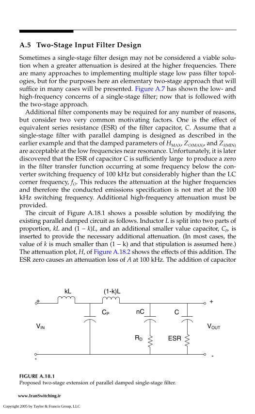
Design Fundamentals of SMPS Input Filters 211
A.5 Two-Stage Input Filter Design
Sometimes a single-stage filter design may not be considered a viable solu-tion when a greater attenuation is desired at the higher frequencies. Thereare many approaches to implementing multiple stage low pass filter topol-ogies, but for the purposes here an elementary two-stage approach that willsuffice in many cases will be presented. Figure A.7 has shown the low- andhigh-frequency concerns of a single-stage filter; now that is followed withthe two-stage approach.
Additional filter components may be required for any number of reasons,but consider two very common motivating factors. One is the effect ofequivalent series resistance (ESR) of the filter capacitor, C. Assume that asingle-stage filter with parallel damping is designed as described in theearlier example and that the damped parameters of HMAX, ZO(MAX), and ZI(MIN)
are acceptable at the low frequencies near resonance. Unfortunately, it is laterdiscovered that the ESR of capacitor C is sufficiently large to produce a zeroin the filter transfer function occurring at some frequency below the con-verter switching frequency of 100 kHz but considerably higher than the LCcorner frequency, fO. This reduces the attenuation at the higher frequenciesand therefore the conducted emissions specification is not met at the 100kHz switching frequency. Additional high-frequency attenuation must beprovided.
The circuit of Figure A.18.1 shows a possible solution by modifying theexisting parallel damped circuit as follows. Inductor L is split into two parts ofproportion, kL and (1 – k)L, and an additional smaller value capacitor, CP, isinserted to provide the necessary additional attenuation. (In most cases, thevalue of k is much smaller than (1 − k) and that stipulation is assumed here.)The attenuation plot, H, of Figure A.18.2 shows the effects of this addition. TheESR zero causes an attenuation loss of A at 100 kHz. The addition of capacitor
FIGURE A.18.1Proposed two-stage extension of parallel damped single-stage filter.
CnC
RD
(1-k)L
VIN VOUT
+
-
+
-
kL
CP
ESR
DK_1137.book Page 211 Wednesday, June 15, 2005 11:49 AM
Copyright 2005 by Taylor & Francis Group, LLC
Copyright 2005 by Taylor & Francis Group, LLC
www.IranSwitching.ir

212 Practical Computer Analysis of Switch Mode Power Supplies
CP, working in conjunction with input inductor, kL, adds an additional two-pole rolloff and restores the additionally required attenuation, A, at 100 kHz;now the conducted emission specification is met. It should be stated here thatonly the high-frequency portion of the filter has been affected; all the previouslydesigned parameters of HMAX, ZO(MAX), and ZI(MIN) at the lower frequency arenegligibly affected. Another aspect of note is that the addition of CP couldproduce a small amount of peaking at the corner frequency of kL and CP;however, this should occur at a frequency significantly lower than the switchingfrequency of 100 kHz, and also considerably higher than the low-frequencycorner of LC. This small effect should not affect filter performance.
A second reason for implementing a two-stage filter is that it might bepossible to reduce the size of the filter physically by using more, but smaller,parts. For example, the low-frequency corner of LC can be raised by loweringthese values (smaller size parts) and producing a four-pole rolloff at thehigher frequencies and it will still provide the necessary attenuation at thehigher switching frequency. Figure A.19 shows a comparison of a single-stagetwo-pole filter and a two-stage four-pole filter implemented by splitting L andadding CP as previously shown. Note that the same attenuation of –49 dB isstill provided at 100 kHz.
If a two-stage implementation is decided upon for whatever reason, itmust be stated that when the values of L and C are selected, the proceduresfor designing the low-frequency damping as shown here are the same asthose used for a single-stage filter.
FIGURE A.18.2Effect of adding CP to compensate for loss of attenuation caused by ESR.
0 dB
100 kHz
- 49 dB
ESR Zero
Attenuation ProducedBy Adding CP
(AttenuationLoss)
H
A
DK_1137.book Page 212 Wednesday, June 15, 2005 11:49 AM
Copyright 2005 by Taylor & Francis Group, LLC
Copyright 2005 by Taylor & Francis Group, LLC
www.IranSwitching.ir

Design Fundamentals of SMPS Input Filters 213
FIGURE A.19Example of a two-stage design increasing the LC corner frequency.
0 dB
100 kHz(Switching Frequency)
- 49 dB
H
One StageLC CornerFrequency
Two StageLC CornerFrequency
(kL)CP
CornerFrequency
DK_1137.book Page 213 Wednesday, June 15, 2005 11:49 AM
Copyright 2005 by Taylor & Francis Group, LLC
Copyright 2005 by Taylor & Francis Group, LLC
www.IranSwitching.ir

Appendix B
Pulse Width Modulator Controller
Macromodeling
For the efficient computer analysis of electronic circuits, a common approachused nowadays is to develop macro or behavioral models representing spe-cific complex functions. When an SMPS that uses a commercially availableintegrated circuit controller is analyzed, it can be convenient and very usefulto utilize a macromodel for this controller. These controllers perform thefunction of pulse width modulation control and are sometimes quite complexwhen all the ancillary functions, such as undervoltage lockout, dead bandcontrol, bias voltage supplies, soft start, and various current-limiting schemes,are included.
These controllers have two basic categories of macros. One will model thecircuit functions explicitly, including the actual pulse width modulator(PWM) switching action. These are helpful when one is looking at the actualreal-time SMPS switching transient performance. The second type of macromodels the circuit-averaged PWM function and does not simulate the actualPWM switching action. This one is compatible with the types of analysis pre-sented in this book and thus is considered in this appendix and in Chapter 6. Ifpossible, a controller macromodel available from the vendor or some othersource may be used for analysis. If not, it will be beneficial to develop onefrom the vendor’s data sheet with the possible use of available test data.This section will develop two representative current mode circuit-averagedmacromodel controllers for use in the SMPS analysis examples presented inChapter 6: the UC1844 and UC1825A current mode PWM controllers.
B.1 UC 1844 Circuit-Averaging Macromodel Development
The manufacturer’s specification for the commercially available UC1842/3/4/5 series of current mode PWM controllers is reproduced at the end of thisappendix. This controller has been in use for several years and may be con-sidered somewhat generic. It is of medium complexity and will serve for
DK_1137.book Page 215 Wednesday, June 15, 2005 11:49 AM
Copyright 2005 by Taylor & Francis Group, LLC
www.IranSwitching.ir

216
Practical Computer Analysis of Switch Mode Power Supplies
purposes of illustration. The block diagram shown in the manufacturer’s spec-ification notes that these controllers have the following general characteristics:
• Internal 5-V bias power supply• Internal 2.5-V precision reference voltage• Input undervoltage lockout circuit• Oscillator• General-purpose op amp for voltage feedback error amplifier• 1.0-V peak current sense comparator• Single-ended output
The UC1844 version of this series has been selected for this developmentexample, but the other versions could be created by simple modifications tothe macromodel being developed. The differences in these versions are themaximum allowed duty ratio and the UVLO trip levels. The internal indi-vidual macromodels will now be developed for the functions listed earlierand then assimilated into one block representing a macromodel of the entirecontroller. A word of caution: no macromodel exactly emulates the circuit itis modeling. Rather, the goal is to replicate the necessary functions withsufficient fidelity so as to be able to perform the desired analysis of theswitching regulator.
The first function to be developed is the input undervoltage lockout. Fromthe manufacturer’s specification, the undervoltage lockout circuit has a typ-ical input start up voltage of 16 V and a typical hysteretic drop out voltageof 10 V. (Maximum or minimum values may be used here if a worst-caseanalysis is desired.) Figure B.1 shows a circuit macro that will generate thisfunction using a simple gain device configured as a voltage comparator withhysteresis. The output of this circuit is 0 V for OFF or 1 V for ON. This unitsignal can be used as a multiplier for the bias and reference supplies to switchthem on and off effectively. The start-up and operating supply current drawis also included as part of this macro.
The next internal macro is the 5-V bias supply. From the specification sheet,this supply will have a nominal line regulation of 6 mV for an input voltagerange of 12 to 25 V or 0.46 mV/V. Nominal load regulation is 6 mV for a loadchange of 1.0 to 20 mA or an equivalent output impedance of 0.32
Ω
. Temper-ature stability is nominally 0.2 mV/
°
C. The 2.5-V reference for the error ampli-fier is simply a 2:1 divider from the 5-V bias. Figure B.2 shows a macro forthis circuit. An output short-circuit current limit of 100 mA is specified; how-ever, for simplicity, this feature is not included. It may be added if desired.
The error amplifier macro is shown in Figure B.3. Although, for the sakeof simplicity, this amplifier macro does not mirror the actual circuit exactly,the following characteristics are felt to be adequate for almost all cases:
• DC gain (avol): 90 dB• Unity gain bandwidth: 1 MHz
DK_1137.book Page 216 Wednesday, June 15, 2005 11:49 AM
Copyright 2005 by Taylor & Francis Group, LLC
www.IranSwitching.ir

Pulse Width Modulator Controller Macromodeling
217
• PSSR (DC) 70 dB• VOH 5.6 V• VOL 0.6 V• IOL 1.3 mA• IOH 1.5 mA
The duty ratio generation macro, here called the duty ratio calculator (DRC),is shown in Figure B.4. The duty ratio,
d
, is determined from Equation 4.6 andEquation 4.7 in Chapter 4 for continuous and discontinuous modes, respectively:
(continuous mode) (4.6)
FIGURE B.1
UC1844 undervoltage lockout (UVLO) macro.
+
+
HystereticSupply Current
UVLOHysteresis
OutputLatch
3
56
VP1
VN1
4
ISUP1M
G5
RIN1K
CG220N
CHOLD20N
G1 G2
G3 G3HYST
G41
RG41
CG41N
X5
X1 X2 X3 X4
GND
UVLOVCCVCC
GND
UVLO
UVLO Output 1V = ON0V = OFF
2
XSUP
di
m L v v
vCR f L
TSL C g
=−
+ −
2
2 2 22( )
DK_1137.book Page 217 Wednesday, June 15, 2005 11:49 AM
Copyright 2005 by Taylor & Francis Group, LLC
www.IranSwitching.ir

218
Practical Computer Analysis of Switch Mode Power Supplies
FIGURE B.2
UC1844 voltage reference (VREF) macro.
FIGURE B.3
UC1844 ERROR AMP macro.
+
3
9
VMR0
IVT3.125
RVT0.32
TC = 0.2E-3
GND
VREF
VCC
VCC
GND
VREF
2
+
+
+ VREF/2
+
+
VREF/2
VT1
EVREF/2
UVLO
UVLO
EUVLOV(1)*V(UVLO)
FUVLO1
EIN0.46E-3
V54.99342
1
4
GND
VIN
+
VCC
++
-
+VIP
256
74 3
8
1
EPSSR
RIN10MEG
GA1K
RG30
IBIAS0.3U
CG0.159M
VNC1
VPC5
RO3K
OUTPUT
GND
DN DP
RPS1E8
DK_1137.book Page 218 Wednesday, June 15, 2005 11:49 AM
Copyright 2005 by Taylor & Francis Group, LLC
www.IranSwitching.ir

Pulse Width Modulator Controller Macromodeling
219
(discontinuous mode) (4.7)
These equations are rearranged for ease of implementation in a computersimulation equation line:
(continuous mode) (6.1)
(discontinuous mode) (6.2)
The duty ratios calculations for the continuous and discontinuous modesare represented in Figure B.4 by GCM and GDCM, respectively. The maxi-mum allowable duty ratio limit is imposed by IDRMAX. These three currentgenerators are then configured in a stacked arrangement so that only theminimum of the three currents is actually monitored in the current-measur-ing source, VMD. The magnitude of this minimum current is numericallyequal to the desired duty ratio,
d
, and is eventually converted to the
d
thatprovides pulse width modulation control of the power converter outputvoltage.
The complete PWM controller macro is shown in Figure B.5. Note that inthe actual controller circuit, certain parameters, such as input voltage (
v
g
);output voltage (
v
); inductance,
L
; slope compensation,
m
C
; and scale factor,
R
f
, are not an
explicit
input to the actual controller block. Their
implicit
effects,however, must be added as an input to the macro controller because thesensed averaged current in the macro does not contain them. The sensedcurrent in the actual physical circuit does contain them. These effects arenecessary for producing the correct duty ratio,
d
, per Equation 4.6 andEquation 4.7.
This macro will be used to analyze some SMPS examples in Chapter 6. Acircuit analysis netlist for the macro of this UC1844 is shown next. Note the
comment
entries. They define and indicate that the equations on the line justbelow them need to have the appropriate values of max duty ratio(
IDRMAX
),
L
,
RF
,
TS
, and
MC
inserted there for the reasons indicated in theprevious paragraph. The ones shown here have representative placeholdervalues inserted for (
IDRMAX
),
L
,
RF
,
TS
, and
MC
. These values in theequations for GCM, GDCM, and IDRMAX must be modified to the actualones used for a particular design.
Also, the line containing VOVRD may need to be inserted when it isdesired to override the UVLO circuit. With the hysteretic latch in the UVLO
dm L v v
vCR f
TSL C g
=+ −
2 2( )
dv i R
m L v v
C L fTSR f
L C g
=−
+ −2
2 2 22( )
dv
m L v vC
TSR fL C g
=+ −
2 2( )
DK_1137.book Page 219 Wednesday, June 15, 2005 11:49 AM
Copyright 2005 by Taylor & Francis Group, LLC
www.IranSwitching.ir

220
Practical Computer Analysis of Switch Mode Power Supplies
macro, it may sometimes be required to prevent nonconvergence when seek-ing a BIAS solution for an AC analysis. The start and stop UVLO trip levelsare set up in lines G1 and G2, respectively. Here the arbitrary maximum startvoltage of 17 V and the typical stop level of 10 V are used. G1 and G2 arein actuality high-gain devices, so the full on and off characteristics areachieved with only a slight control voltage change above the start trip level
FIGURE B.4
UC1844 duty ratio calculator macro.
C
12
6
7
4
8
GL1
++ +
13
GND
+
+3
1
GND
C
1110
1A
GDCM
GCM
IDRMAX0.48
REL1E8
D2L
D1L
VLMIN1
DX1
DX2
DX3DX4
DX5d
d
VMD0V
EMD RMD1K
14
UVLO
V
VG
ISENSE
COMP
9
RLIM1
R1200K
R2100K
X1 X2
VLIM1
+
-
6A
DK_1137.book Page 220 Wednesday, June 15, 2005 11:49 AM
Copyright 2005 by Taylor & Francis Group, LLC
www.IranSwitching.ir

Pulse W
idth Modulator C
ontroller Macrom
odeling
221
FIGURE B.5
UC1844 PWM controller macro.
CCV UVLO
DNG
LVUX O
PMOC
SNESI E
V
GV
CRDX
VU LO
DNG
d
RL F TS CM
PIV
NIV
CV C
DNGTUPTUO
OLVU
CCV
RV EF/2
RV EF
FERX
DNG
3
4
6 78
d
OC PM
RV FE /2
LVU O
NG D
CCV
DNG
ERV F
FV B
MOC PRUC TNER
SNES E
VGV
d
CV C
ARREX MP
DK
_1137.book Page 221 Wednesday, June 15, 2005 11:49 A
M
Copyright 2005 by T
aylor & Francis G
roup, LL
C
www.IranSwitching.ir

222
Practical Computer Analysis of Switch Mode Power Supplies
or below the stop trip level. G1 and G2 values for UVLO start and stopvalues are indicated.
***UC 1844 PWM CONTROLLER CIRCUIT AVERAGING MACRO.SUBCKT UC1844 VCC 3 4 COMP 6 7 8 d GND* VCC VREF VFB COMP ISENSE V VG d GND**NOTE: ALL SIGNAL INPUTS MUST BE REFERENCED TO THE UC1844 GND XUVLO VCC UVLO GND UVLOXREF UVLO VCC 3 VREF/2 GND REFXERRAMP 4 VREF/2 VCC COMP GND ERRAMPXDRC COMP d 6 7A 8A UVLO GND DRC**DEPENDENT GENERATORS FOR GROUND ISOLATION IF DESIREDEVG 8A 0 8 GND 1EV 7A 0 7 GND 1.ENDS UC1844*.SUBCKT DRC 1 d 8 9 10 14 GND* COMP d ISENSE V VG UVLO GNDVBK 1 1A DC 2 R1 1A C 200KR2 C GND 100KX1 C 3 DIDEALX2 GND C DIDEALVLIM 3 GND DC 1RCONV1 6 0 1GRCONV2 7 0 1GRCONV3 4 0 1G*REL 10 9 1E8GL 0 11 10 9 1D1L 11 12 DXD2L 0 11 DXRLMIN 12 13 1VLMIN 13 0 1U*DX1 4 0 DXDX2 7 4 DXDX3 6 7 DX***IDRMAX VALUE = MAX LIMITED DUTY RATIOIDRMAX 7 6 DC .48DX4 0 6 DXDX5 6 6A DXVMD 6A 0EMD d 0 VALUE = I(VMD)*V(14)+1PRMD d 0 1.MODEL DX D IS=1E-12**L = 40U*RF = 0.3*TS = 10U*MC = .3E6*
DK_1137.book Page 222 Wednesday, June 15, 2005 11:49 AM
Copyright 2005 by Taylor & Francis Group, LLC
www.IranSwitching.ir

Pulse Width Modulator Controller Macromodeling
223
**GCM 4 7 VALUE = (V(C)-RF*V(8))/((TS*RF)/(2*L))*(2*MC*L+V(12)))GCM 4 7 VALUE = LIMIT((V(C)-0.3*V(8))/((10U*0.3)/(2*40U)*(2*.3E6*40U+V(12))),0,1)***GDCM 0 4 VALUE = V(C)/((TS*RF/L)*(MC*L+V(12))GDCM 0 4 VALUE = LIMIT(V(C)/((10U*0.3/40U)*(.3E6*40U+V(12))),0,1)*.ENDS DRC*.SUBCKT UVLO VCC UVLO GND* VCC UVLO GNDRIN VCC 2 1KISUP 2 GND 1MXSUP GND 2 DIDEALG5 VCC GND VALUE = .01*V(UVLO,GND)** G1 AND G2 SET UVLO START AND STOP LEVELS RESPECTIVELY** START = 17** STOP = 10G1 0 3 TABLE V(VCC,GND) = (0,0) (17,0) (18,20)G2 3 0 TABLE V(VCC,GND) = (9,20) (10,0) (17,0)CG2 3 0 20NR1 3 0 1E3G3 0 4 3 0 1G3HYST 0 4 VALUE = -100U+200U*V(UVLO,GND)CHOLD 4 0 20NG4 GND UVLO 4 GND 1**VOVRD TO BE INSERTED FOR UVLO OVERRIDE*VOVRD UVLO GND DC 1RG4 UVLO GND 1CG4 UVLO GND 1NX5 GND UVLO DIDEALX1 3 5 DIDEALX2 6 3 DIDEALX3 4 5 DIDEALX4 6 4 DIDEALVP 5 0 DC 1VN 0 6 DC 1.ENDS UVLO**5.0 VOLT REFERENCE MACRO.SUBCKT REF UVLO VCC VREF VREF/2 GND* UVLO VCC VREF VREF/2 GND* EIN 2 3 VCC GND .46E-3RVT 3 4 .32 TC=0.2E-3IVT GND 3 DC 3.125 VT GND 4 DC 1V5 1 2 DC 4.99342FUVLO 1 GND VMR 1EUVLO VREF 9 VALUE = V(1,GND)*V(UVLO,GND)VMR GND 9EVREF/2 VREF/2 GND VREF GND .5.ENDS REF**ERROR AMP MACRO
DK_1137.book Page 223 Wednesday, June 15, 2005 11:49 AM
Copyright 2005 by Taylor & Francis Group, LLC
www.IranSwitching.ir

224
Practical Computer Analysis of Switch Mode Power Supplies
.SUBCKT ERRAMP 6 7 8 1 GND * VIN VIP VCC OUTPUT GNDRIN 5 7 10MEGEPSRR 6 5 VALUE = (V(8)-15)*3E-4IBIAS 5 GND .3UGA GND 2 7 5 1KRG 2 GND 30CG 2 GND 0.159MVNC 4 GND DC 1DN 4 2 D1VPC 3 GND DC 5DP 2 3 D1RO 1 2 3KRPS 8 0 1E8.ENDS ERRAMP.MODEL D1 D IS=1E-9*******************************************************.SUBCKT DIDEAL 1 2VAS 1 3 DC -1uD1 3 2 DD2 3 4 DD3 4 2 D1FAS 4 2 VAS 1.MODEL D D IS=1E-6 EG=0 XTI=-4.MODEL D1 D EG=0 XTI=0CC 1 2 .1P.ENDS DIDEAL*
B.2 UC 1825A Circuit-Averaging Macromodel Development
The manufacturer ’s specification for the commercially availableUC1823A,B/1825A,B series of current mode PWM controllers is reproducedat the end of this appendix. This controller has been in use for several yearsand has definitely attained the status of industry standard. It is more complexthan the previously examined UC1844 and contains almost all of the generaldesirable features needed when an SMPS is to be designed. The block dia-gram shown in the manufacturer’s specification notes that these controllershave the following general characteristics:
• Internal 5.1-V precision reference and bias power supply• Input undervoltage lockout (UVLO) circuit• Soft start circuit• Oscillator• General-purpose op amp for voltage feedback error amplifier
DK_1137.book Page 224 Wednesday, June 15, 2005 11:49 AM
Copyright 2005 by Taylor & Francis Group, LLC
www.IranSwitching.ir

Pulse Width Modulator Controller Macromodeling
225
• Current limit (cycle by cycle with no soft start reset)• Current limit (with soft start reset hiccup mode)
The UC1825A version of this device has been selected for this example;however, the other versions could be created by simple modifications ofthe UVLO limits and the maximum duty ratio stipulation to the macro-model being developed. Now the internal individual macromodels willnow be developed for the functions listed earlier and then assimilated intoone block representing a macromodel of the entire controller. Again, a wordof caution: no macromodel exactly emulates the circuit it is modeling.Rather, the goal is to replicate the necessary functions with sufficient fidel-ity so as to be able to perform the desired analysis of the switching regu-lator. Because an averaging model is being developed, the oscillator andexplicit pulse by pulse current limiting features are, of course, not includedin this model.
The first function to be developed is the input undervoltage lockout. Fromthe manufacturer’s specification, the undervoltage lockout circuit has a typ-ical input start up voltage of 9.2 V and a typical hysteretic dropout or stopvoltage of 8.4 V. (Maximum or minimum values may be used here if a worst-case analysis is desired.) Figure B.6 shows a circuit macro that will generatethis function using a simple gain device configured as a voltage comparatorwith hysteresis. The output of this circuit is 0 V for OFF or 1 V for ON. Thisunit signal can be used as a multiplier for the bias and reference supplies toswitch them on and off effectively. It is also used as an on–off control signalin the soft start, overcurrent, voltage reference bias supply, and duty ratiocontrol circuits. The start-up and operating supply current draw is alsoincluded as part of this macro.
The next internal macro is the 5.1-V reference bias supply. From the spec-ification sheet, this supply will have a nominal line regulation of 2 mV foran input voltage range of 12 to 20 V or 0.25 mV/V. Nominal load regulationis 5 mV for a load change of 1.0 to 10 mA or an equivalent output impedanceof 0.56
Ω
. Temperature stability is nominally 0.2 mV/
°
C. Figure B.7 showsa macro for this circuit. An output short-circuit current limit of 60 mA isspecified; however, for simplicity, this feature is not included. A circuitmodification to provide this limit may be added if desired.
The error amplifier macro is shown in Figure B.8. Although, for the sakeof simplicity, this amplifier macro does not mirror the actual circuit exactly,the following characteristics are felt to be adequate for almost all cases:
• DC gain (avol): 95 dB• Unity gain bandwidth: 12 mHz• PSSR (DC) 95 dB• VOH 4.7 V• VOL 0.6 V
DK_1137.book Page 225 Wednesday, June 15, 2005 11:49 AM
Copyright 2005 by Taylor & Francis Group, LLC
www.IranSwitching.ir

226
Practical Computer Analysis of Switch Mode Power Supplies
• IOL
≤
1.0 mA• IOH
≤
1.0 mA
The soft start and overcurrent macro is shown in Figure B.9. At first glance,the macro may seem a little daunting, but with a good understanding of theactual soft start and overcurrent operation of the physical UC1825A fromthe manufacturer’s data sheet, the macro’s similarity is readily understood.As in the actual unit, the soft start timing capacitor is connected to the SSpin. This circuit functions by basically pulling the E/A OUT (or COMP, asit is commonly known) low whenever the UVLO indicates that a pre-start-up condition exists or if an overcurrent condition has been sensed. With thiscondition, a hiccup attempted recovery mode is established by rapidly dis-charging the soft start capacitor and then slowly recharging it during theattempted soft start-up mode. With the required sensing of peak currents inthe converter for an overcurrent shutdown, a peak current calculator is
FIGURE B.6
UC1825A undervoltage lockout (UVLO) macro.
+
+
HystereticSupply Current
UVLOHysteresis
OutputLatch
3
56
VP1
VN1
4
ISUP0.1M
G5
RIN1K
CG220N
CHOLD20N
G1 G2
G3 G3HYST
G41
RG41
CG41N
X5
X1 X2 X3 X4
GND
UVLOVCCVCC
GND
UVLO
UVLO Output 1V = ON0V = OFF
2
XSUP
DK_1137.book Page 226 Wednesday, June 15, 2005 11:49 AM
Copyright 2005 by Taylor & Francis Group, LLC
www.IranSwitching.ir

Pulse Width Modulator Controller Macromodeling
227
FIGURE B.7
UC1825A voltage reference (VREF) macro.
FIGURE B.8
UC1825 ERROR AMP macro.
+
3
9
VMR0
IVT1.786
RVT0.56
TC = 0.2E-3
GND
VREF
VCC
VCC
GND
VREF
2
+
+
+ VREF/2
+
+
VREF/2
VT1
EVREF/2
UVLO
UVLO
EUVLOV(1)*V(UVLO)
FUVLO1
EIN0.25E-3
V55.097555
1
4
GND
VIN
+
VCC
++
-
+VIP
256
74 3
8
1
EPSSR3E-5
RIN10MEG
GA1K
RG56
IBIAS0.6U
CG13U
VNC1
VPC4.1
RO10
OUTPUT
GND
DN DP
RPS1E8
DK_1137.book Page 227 Wednesday, June 15, 2005 11:49 AM
Copyright 2005 by Taylor & Francis Group, LLC
www.IranSwitching.ir

228
Practical C
omputer A
nalysis of Switch M
ode Pow
er Supplies
FIGURE B.9
UC1825A soft start and overcurrent macro.
DK
_1137.book Page 228 Wednesday, June 15, 2005 11:49 A
M
Copyright 2005 by T
aylor & Francis G
roup, LL
C
www.IranSwitching.ir

Pulse Width Modulator Controller Macromodeling
229
necessary because the circuit-averaging macro only generates averagedcurrents.
The peak discontinuous mode current for the buck topology is expressedby Equation 3.2 and, for the boost and buck–boost topologies, by Equation 3.5.The continuous mode peak current is simply equal to the averaged or DCvalue of current plus one-half of the value expressed by the discontinuousmode peak value calculation. The peak current calculator circuit in Figure B.9continuously calculates the continuous and discontinuous mode values ofpeak current; the larger of the two appears on node IPK. This is the correctvalue of peak current that the actual switching converter will produce andis valid for these calculations.
When the 1.2-V overcurrent threshold is sensed by the overcurrent sensecomparator, the fault latch is subsequently tripped; this eventually turns ongenerator GLS (the 250-
µ
A source). This pulls the SS and COMP pins low,shutting down the converter. A shutdown signal, SD, is also fed from thefault latch over to the DRC to reduce the duty ratio
d
of the converterimmediately to zero. When the SS pin voltage drops below the 0.2-V thresh-old of the SS restart comparator, the fault latch and the restart latch are reset.This turns current sink GLS off, allowing the soft start capacitor to rechargefrom the 9-
µ
A source, ITS. This allows the COMP pin to increase slowly,thus implementing a soft restart.
In the actual controller, a 1.0-V current limit comparator is used for pulse-by-pulse current limiting. This is obviously not possible to implement explic-itly with the circuit-averaged simulation. For the sake of simplicity, thiscurrent limit comparator is not implemented; however, the output of theovercurrent sense comparator (threshold equal to 1.2 V) is used basically toimplement the same function of rapid shutdown. Its output, CL, is feddirectly to the duty ratio calculator to reduce the duty ratio
d
immediatelyto zero. This may be considered a practical approximation to the operationof the actual controller.
In many practical designs, noise or overshoot on the current sense circuit(ILIM input) tends to make these two trip levels of 1.0 and 1.2 dynamicallyindistinguishable and the shutdown and soft restart cycle occurs withoutactually noting any sustained pulse-by-pulse current limiting. (If it is deemednecessary to implement the 1.0 current limit rapid shutdown, instructionson how to accomplish this are shown in the macro netlist at the end of thissection. This involves removing source G1 from the soft start macro, therebydisabling the overcurrent latch, and then reducing the threshold sense ofsource IPK from 1.2 to 1.0 amps.) In some designs, pulse-by-pulse currentlimiting may be provided by a saturated high value of the E/A OUT signallimiting the peak current before the 1.0 and 1.2 comparator thresholds arereached. Also, the ILIM input may be connected to ground, thus eliminatingany explicit pulse-by-pulse current limiting or overcurrent hiccup mode ofoperation if desired.
At this point, a note about the implementation of the digital circuit func-tions of the soft start macro model of Figure B.9 must be made. Nowadays,
DK_1137.book Page 229 Wednesday, June 15, 2005 11:49 AM
Copyright 2005 by Taylor & Francis Group, LLC
www.IranSwitching.ir

230
Practical Computer Analysis of Switch Mode Power Supplies
most circuit simulators provide for mixed mode simulations using analogand digital components. The mixed mode is not used here, however. Becausethe digital logic functions in the controller are not very complex, it wasdecided to implement them with basic analog circuit components that allcircuit simulators possess. This was done to provide a most basic and alter-native approach to the model. It is a relatively easy transformation of themacro for anyone who might be interested in modifying it for use with amixed mode simulator.
The duty ratio generation macro, duty ratio calculator (DRC), is shown inFigure B.10 and uses the same basic algorithms as the one used in the UC1844macro derived earlier. A significant difference is that the peak current senseunit control signal,
CL
, from the soft start, overcurrent macro is fed over toreduce the duty ratio,
d
, to zero, thus shutting off the converter. The SDsignal from the soft start fault latch is also fed over to reduce the converterduty ration to zero.
The complete UC1825A PWM controller macro is shown in Figure B.11.As was the case for the previous UC1844 macro, certain parameters, such asinput voltage (
v
g
); output voltage (
v
); inductance,
L
; slope compensation,
m
C
;and scale factor,
R
f
, are not an explicit input to the actual controller block.Their implicit effects, however, must be added as an input to the macrocontroller because the sensed averaged current in this macro does not containthem. The sensed current in the actual physical circuit does contain them.These effects are necessary for producing the correct duty ratio,
d
, perEquation 4.6 and Equation 4.7.
This macro will also be used to analyze an SMPS example in Chapter 6.A circuit analysis netlist for the macro of this UC1825A is shown next. Notethe
comment
entries. In some cases, they define and indicate that the equa-tions on the line just below them need to have the appropriate values of maxduty ratio (
IDRMAX
),
L
,
RF
,
TS
,
MC
, and
RLIM
inserted there for the reasonsindicated in the previous paragraph. The ones shown here have representa-tive placeholder values inserted for (
IDRMAX
),
L
,
RF
,
TS
,
MC
, and
RLIM
.These values in the equations for GCM, GDCM, IDRMAX, and GIPK mustbe modified to the actual ones used for a particular design.
When a BIAS solution, possibly for an AC analysis, is sought, it maysometimes be necessary to override the UVLO circuit. With the hystereticlatch in the UVLO macro, nonconvergence problems can arise when seekinga BIAS solution. To accomplish this, a unit voltage source, VOVRD, of 1 Vis inserted at the node where the normal UVLO signal would exist. The linein the netlist containing VOVRD indicates the action required when it isdesired to override the UVLO circuit.
Additionally, the soft start subcircuit, XSOFTSTART, will in most casesneed to be removed from the netlist when BIAS solutions are sought. Withthe hysteretic nature of the R–S latches in this soft start macro, this removalwill usually be required to prevent nonconvergence when a BIAS solutionfor an AC analysis is sought. The nonconvergent problems caused by the bi-state nature of these latches may be prevented without actually removing
DK_1137.book Page 230 Wednesday, June 15, 2005 11:49 AM
Copyright 2005 by Taylor & Francis Group, LLC
www.IranSwitching.ir

Pulse Width Modulator Controller Macromodeling
231
them from the circuit. One way might be by possibly using the NODESETcommand along with some limiting functions or components. The mostpractical way, however, is simply to remove them from the circuit as is donehere. After all, soft start and UVLO are functions considered only whentransient analyses are conducted and not when AC analyses are performed.
FIGURE B.10
UC1825A duty ratio calculator macro.
C
12
6
7
4
8
GL1
++ +
13
GND
+1
GND
1110
GDCM
GCM
IDRMAX0.48
REL1E8
D2L
D1L
VLMIN1
DX1
DX2
DX3DX4
DX5d
d
VMD0V
EMD
RMD1K
14UVLO
V
VG
ISENSE
COMP
9
RLIM1
R21E6
+
-
VCS1.25
C
6A
CL
SD
DK_1137.book Page 231 Wednesday, June 15, 2005 11:49 AM
Copyright 2005 by Taylor & Francis Group, LLC
www.IranSwitching.ir

232
Practical C
omputer A
nalysis of Switch M
ode Pow
er Supplies
FIGURE B.11
UC1825A PWM controller macro.
CCV U LV O
NG D
LVUX O
PMOC
IS ESNE
V
GV
CRDX
OLVU
DNG
d
RL F TS MC
PIV
NIV
CV C
DNGTUO P TU
OLVU
CV C V ER FFERX
DNG
3
4
6 78
d
OC PM
VU OL
NG D
CCV
NG D
ERV F
IN
/E TUO ASI ESNE
VGV
d
SSSS
VNI
V“ ”
V“ ”G
V“ ” “VG”
5
CV C
EX PMARR
LCDS
IS ESNE
FOSX T TS TRA
OLVU
RV EF
MOC P
d
SS
RL F ST
VV G
DNGLCDS
DK
_1137.book Page 232 Wednesday, June 15, 2005 11:49 A
M
Copyright 2005 by T
aylor & Francis G
roup, LL
C
www.IranSwitching.ir

Pulse Width Modulator Controller Macromodeling
233
The start and stop UVLO trip levels are set up in lines G1 and G2, respec-tively. Here an arbitrary nominal start voltage of 9.2 V and the typical stoplevel of 8.4 V are used. G1 and G2 are in actuality high-gain devices, so thefull on and off characteristics are achieved with only a slight control voltagechange above the start trip level or below the stop trip level.
***UC1825A PWM CONTROLLER CIRCUIT AVERAGING MACRO.SUBCKT UC1825A VCC 3 4 5 COMP 6 SS 7 8 D GND* VCC VREF INV NI E/A_OUT RAMP SS V VG d GND**NOTE: ALL SIGNAL INPUTS MUST BE REFERENCED TO THE UC1825A GND XUVLO VCC UVLO GND UVLOXREF UVLO VCC 3 GND REFXERRAMP 4 5 VCC COMP GND ERRAMPXDRC COMP d 6 7A 8A UVLO SD CL GND DRC** NOTE: SUBCKT “XSOFTSTART” SHOULD BE REMOVED FOR BIAS SOLUTIONSXSOFTSTART 6 7A 8A 3 UVLO d COMP SS SD CL GND SOFTSTARTRSSCKT SS GND 1E9**DEPENDENT GENERATORS FOR GROUND ISOLATION IF DESIREDEVG 8A 0 8 GND 1EV 7A 0 7 GND 1.ENDS UC1825A*.SUBCKT DRC C d 1 9 10 14 SD CL GND* COMP d ISENSE V VG UVLO SD CL GNDRCONV1 6 0 1GRCONV2 7 0 1GRCONV3 4 0 1GR2 C GND 1E6VCS 8 1 DC 1.25*REL 10 9 1E8GL 0 11 10 9 1D1L 11 12 DXD2L 0 11 DXRLMIN 12 13 1VLMIN 13 0 1U*DX1 4 0 DXDX2 7 4 DXDX3 6 7 DX***IDRMAX VALUE = MAX LIMITED DUTY RATIOIDRMAX 7 6 DC .48DX4 0 6 DXDX5 6 6A DX.MODEL DX D IS=1E-12VMD 6A 0EMD d 0 VALUE = LIMIT(I(VMD)*(1-V(CL))*V(14)*(1-V(SD)),1U,.99)RMD d 0 1***PULL DOWNS THAT ARE REQUIRED WHEN XSOFTSTART IS REMOVED FROM CIRCUITRCL CL 0 1E3IRCL 0 CL DC 1P
DK_1137.book Page 233 Wednesday, June 15, 2005 11:49 AM
Copyright 2005 by Taylor & Francis Group, LLC
www.IranSwitching.ir

234
Practical Computer Analysis of Switch Mode Power Supplies
RSD SD 0 1E3IRSD 0 SD DC 1P**L = 50U*RF = .5*TS = 10U*MC = 0***GCM 4 7 VALUE = (V(C)-RF*V(8))/((TS*RF)/(2*L))*(2*MC*L+V(12)))GCM 4 7 VALUE = LIMIT((V(C)-.5*V(8))/((10U*.5)/(2*50U)*(2*0*50U+V(12))),0,1)***GDCM 0 4 VALUE = V(C)/((TS*RF/L)*(MC*L+V(12))GDCM 0 4 VALUE = LIMIT(V(C)/((10U*.5/50U)*(0*50U+V(12))),0,1)*.ENDS DRC*.SUBCKT UVLO VCC UVLO GND* VCC UVLO GNDRIN VCC 2 1KISUP 2 GND .1MXSUP GND 2 DIDEALG5 VCC GND VALUE = .028*V(UVLO,GND)**G1 AND G2 SET UVLO START AND STOP LEVELS RESPECTIVELY**START = 9.2**STOP = 8.4G1 0 3 TABLE V(VCC,GND) = (0,0) (9.2,0) (10.2,30)G2 3 0 TABLE V(VCC,GND) = (7.4,30) (8.4,0) (9.2,0)CG2 3 0 20NR1 3 0 1E3G3 0 4 3 0 1G3HYST 0 4 VALUE = -100U+200U*V(UVLO,GND)CHOLD 4 0 20NG4 GND UVLO 4 GND 1**VOVRD TO BE INSERTED FOR UVLO OVERRIDE*VOVRD UVLO GND DC 1RG4 UVLO GND 1CG4 UVLO GND 1NX5 GND UVLO DIDEALX1 3 5 DIDEALX2 6 3 DIDEALX3 4 5 DIDEALX4 6 4 DIDEALVP 5 0 DC 1VN 0 6 DC 1.ENDS UVLO**5.0 VOLT REFERENCE MACRO.SUBCKT REF UVLO VCC VREF GND* UVLO VCC VREF GND* EIN 2 3 VCC GND .25E-3RVT 3 4 .56 TC=0.2E-3IVT GND 3 DC 1.786 VT GND 4 DC 1V5 1 2 DC 5.097555
DK_1137.book Page 234 Wednesday, June 15, 2005 11:49 AM
Copyright 2005 by Taylor & Francis Group, LLC
www.IranSwitching.ir

Pulse Width Modulator Controller Macromodeling
235
FUVLO 1 GND VMR 1EUVLO VREF 9 VALUE = V(1,GND)*V(UVLO,GND)VMR GND 9.ENDS REF**ERROR AMP MACRO.SUBCKT ERRAMP 6 7 8 1 GND * VIN VIP VCC OUTPUT GNDRIN 6 7 10MEGEPSRR 6 5 VALUE = (V(8)-12)*3E-5IBIAS 5 GND .6UGA GND 2 7 6 1KRG 2 GND 56CG 2 GND 13UVNC 4 GND DC 1.1DN 4 2 D1VPC 3 GND DC 4.1DP 2 3 D1RO 1 2 10RPS 8 0 1E8.ENDS ERRAMP.MODEL D1 D IS=1E-9 *.SUBCKT SOFTSTART ISENSE V VG VREF UVLO d C SS 11 8 GND* ISENSE V VG VREF UVLO d C SS SD CL GND*** L = 50U** RF = .5** TS = 10U***PEAK CURRENT CALCULATOR**EPKDCM 15 0 VALUE = V(d)*(V(VG)-V(V))*(TS/L)*RF**NOTE: V(V) IS ZERO FOR ALL TOPOLOGIES EXCEPT THE BUCK** THE BUCK EQUATION IS SHOWN HERE FOR THE GENERAL CASEEPKDCM 15 0 VALUE = V(d)*(V(VG)-V(V))*(10U/50U)*.5XPKDCM 15 IPK DIDEALXPKCCM 16 IPK DIDEALE4 16 17 15 0 .5EPKCCM 17 0 ISENSE 0 1RPK IPK 0 1E3***OVER CURRENT SENSE COMPARATOR 1.2** RLIM = 0.5**GIPK 0 8 VALUE = V(IPK)*RLIMGIPK 0 8 VALUE = V(IPK)*.5XP1 0 8 DIDEALIPK 8 0 DC 1.2XP2 8 6 DIDEALV12 6 0 DC 1EUV 6 19 UVLO GND 1***OR GATE** NOTE: G1 MAY BE REMOVED HERE TO DISABLE “HICCUP” CURRENT LIMIT MODE.** AN EQUIVALENT OF PULSE-BY-PULSE CURRENT LIMITING WILL RESULT.** THE VALUE OF IPK ABOVE MAY BE CHANGED FROM 1.2 TO 1.0 TO THE
DK_1137.book Page 235 Wednesday, June 15, 2005 11:49 AM
Copyright 2005 by Taylor & Francis Group, LLC
www.IranSwitching.ir

236
Practical Computer Analysis of Switch Mode Power Supplies
** ACTUAL CURRENT LIMIT COMPARATOR THRESHOLD IF DESIRED.G1 0 9 8 0 2G2 0 9 19 0 2X2 0 9 DIDEALIOR 9 0 DC 1XR 9 7 DIDEALVOR 7 0 DC 1***AND/OR LOGICG3 0 4 11 0 .75 G4 0 4 2 0 .75G5 0 4 19 GND 1.5X5 0 4 DIDEALIOL 4 0 DC 1X6 4 5 DIDEALV6 5 0 DC 1***SS RESTART COMPARATORGSS 10 0 SS GND 1XR1 0 10 DIDEALIRS2 0 10 DC .2XR2 10 1 DIDEALVP2 1 0 DC 1**SS COMPLETE COMPARATORG5P 0 2 SS 0 1XS1 0 2 DIDEALI5P 2 0 DC 5XS2 2 3 DIDEALVP3 3 0 DC 1**SS/COMPXCP C 18 DIDEALECOMP 18 GND SS GND 1ITS 0 SS DC 9UGLS SS GND VALUE = LIMIT(V(13)*250U,1U,260U)XCLPH SS VREF DIDEALXCLPL GND SS DIDEAL.MODEL D D*XRS1 10 9 11 12 GND RS-LATCHXRS2 12 4 13 14 0 RS-LATCH*.ENDS SOFTSTART*.SUBCKT RS-LATCH R S Q QBAR GNDGR 3 GND R GND 1GS GND 3 S GND 1C3 3 GND 20NG4 GND Q 3 GND 1CG4 Q GND 20NGHYS GND 3 VALUE = –100U+200U*V(Q,GND)GRS GND Q VALUE = .75*(V(R,GND)+V(S,GND))X1 GND Q DIDEALX2 Q 5 DIDEAL
DK_1137.book Page 236 Wednesday, June 15, 2005 11:49 AM
Copyright 2005 by Taylor & Francis Group, LLC
www.IranSwitching.ir

Pulse Width Modulator Controller Macromodeling
237
X3 6 3 DIDEALX4 3 5 DIDEALEINV 5 QBAR VALUE = V(Q)*(1-V(R)*V(S))VN GND 6 DC 1VP 5 GND DC 1.ENDS RS-LATCH*.SUBCKT DIDEAL 1 2VAS 1 3 DC -1uD1 3 2 DD2 3 4 DD3 4 2 D1FAS 4 2 VAS 1.MODEL D D IS=1E-6 EG=0 XTI=-4 .MODEL D1 D EG=0 XTI=0 CC 1 2 .1P.ENDS DIDEAL*
DK_1137.book Page 237 Wednesday, June 15, 2005 11:49 AM
Copyright 2005 by Taylor & Francis Group, LLC
www.IranSwitching.ir

238
Practical Computer Analysis of Switch Mode Power Supplies
DK_1137.book Page 238 Wednesday, June 15, 2005 11:49 AM
Copyright 2005 by Taylor & Francis Group, LLC
www.IranSwitching.ir

Pulse Width Modulator Controller Macromodeling
239
DK_1137.book Page 239 Wednesday, June 15, 2005 11:49 AM
Copyright 2005 by Taylor & Francis Group, LLC
www.IranSwitching.ir

240
Practical Computer Analysis of Switch Mode Power Supplies
DK_1137.book Page 240 Wednesday, June 15, 2005 11:49 AM
Copyright 2005 by Taylor & Francis Group, LLC
www.IranSwitching.ir

Pulse Width Modulator Controller Macromodeling
241
DK_1137.book Page 241 Wednesday, June 15, 2005 11:49 AM
Copyright 2005 by Taylor & Francis Group, LLC
www.IranSwitching.ir

242
Practical Computer Analysis of Switch Mode Power Supplies
DK_1137.book Page 242 Wednesday, June 15, 2005 11:49 AM
Copyright 2005 by Taylor & Francis Group, LLC
www.IranSwitching.ir

Pulse Width Modulator Controller Macromodeling
243
DK_1137.book Page 243 Wednesday, June 15, 2005 11:49 AM
Copyright 2005 by Taylor & Francis Group, LLC
www.IranSwitching.ir

244 Practical Computer Analysis of Switch Mode Power Supplies
DK_1137.book Page 244 Wednesday, June 15, 2005 11:49 AM
Copyright 2005 by Taylor & Francis Group, LLC
www.IranSwitching.ir

Pulse Width Modulator Controller Macromodeling 245
DK_1137.book Page 245 Wednesday, June 15, 2005 11:49 AM
Copyright 2005 by Taylor & Francis Group, LLC
www.IranSwitching.ir

246 Practical Computer Analysis of Switch Mode Power Supplies
DK_1137.book Page 246 Wednesday, June 15, 2005 11:49 AM
Copyright 2005 by Taylor & Francis Group, LLC
www.IranSwitching.ir

Pulse Width Modulator Controller Macromodeling 247
DK_1137.book Page 247 Wednesday, June 15, 2005 11:49 AM
Copyright 2005 by Taylor & Francis Group, LLC
www.IranSwitching.ir

248 Practical Computer Analysis of Switch Mode Power Supplies
DK_1137.book Page 248 Wednesday, June 15, 2005 11:49 AM
Copyright 2005 by Taylor & Francis Group, LLC
www.IranSwitching.ir

Pulse Width Modulator Controller Macromodeling 249
DK_1137.book Page 249 Wednesday, June 15, 2005 11:49 AM
Copyright 2005 by Taylor & Francis Group, LLC
www.IranSwitching.ir
250 Practical Computer Analysis of Switch Mode Power Supplies
DK_1137.book Page 250 Wednesday, June 15, 2005 11:49 AM
Copyright 2005 by Taylor & Francis Group, LLC
www.IranSwitching.ir

Pulse Width Modulator Controller Macromodeling 251
DK_1137.book Page 251 Wednesday, June 15, 2005 11:49 AM
Copyright 2005 by Taylor & Francis Group, LLC
www.IranSwitching.ir

252 Practical Computer Analysis of Switch Mode Power Supplies
DK_1137.book Page 252 Wednesday, June 15, 2005 11:49 AM
Copyright 2005 by Taylor & Francis Group, LLC
www.IranSwitching.ir