Embed Size (px)
Citation preview

PR29MF21NSZ SeriesPR39MF2xNSZ Series
Features
IT(rms)≤0.9A, Zero Cross typeDIP 8pinTriac output SSR
1. Output current, IT(rms)≤0.9A2. Zero crossing functionary (VOX : MAX. 35V)3. 8 pin DIP package (SMT gullwing also available)4. High repetitive peak off-state voltage
(VDRM : 600V, PR39MF2xNSZ Series)(VDRM : 400V, PR29MF21NSZ Series)
5. IFT ranks avai lable (see Model Line-up in this datasheet)
6. Superior noise immunity (dV/dt : MIN. 100V/µs)7. Response time, ton : MAX. 50µs8. High isolation voltage between input and output (Viso(rms) : 4.0kV)
DescriptionPR29MF21NSZ Series and PR39MF2xNSZ Series
Solid State Relays (SSR) are an integration of an infrared emitting diode (IRED), a Phototriac Detector and a main output Triac. These devices are ideally suited for controlling high voltage AC loads with solid state re l iabi l i ty whi le provid ing 4.0kV isolat ion (Viso(rms)) from input to output.
1
Notice The content of data sheet is subject to change without prior notice.In the absence of confirmation by device specification sheets, SHARP takes no responsibility for any defects that may occur in equipment using any SHARP devices shown in catalogs, data books, etc. Contact SHARP in order to obtain the latest device specification sheets before using any SHARP device.
PR29MF21NSZ SeriesPR39MF2xNSZ Series
Sheet No.: D4-A00701FENDate Mar. 31. 2004
© SHARP Corporation
Agency approvals/Compliance
1. Isolated interface between high voltage AC devices and lower voltage DC control circuitry.
2. Switching motors, fans, heaters, solenoids, and valves.
3. Power control in applications such as lighting and temperature control equipment.
Applications
1. Recognized by UL508, file No. E94758 (as model No. R29MF2/R39MF2)
2. Approved by CSA 22.2 No.14, file No. LR63705 (as model No. R29MF2/R39MF2)
3. Optionary available VDE approved (∗)(DIN EN 60747-5-2), file No. 40008898 (only for PR39MF2xNSZ Series as model No. R39MF2)
4. Package resin : UL flammability grade (94V-0)
(∗) DIN EN60747-5-2 : successor standard of DIN VDE0884. Up to Date code "RD" (December 2003), approval of DIN VDE0884.From Date code "S1" (January 2004), approval of DIN EN60747-5-2.
∗Non-zero cross type is also available.(PR29MF1xNSZ Series/PR39MF1xNSZ Series)

Internal Connection Diagram
1
68
1 2 3 4
5
2
3
4
CathodeAnodeCathodeCathode
5
6
8
GateOutput (T1)Output (T2)
Zero Crossing Circuit
2
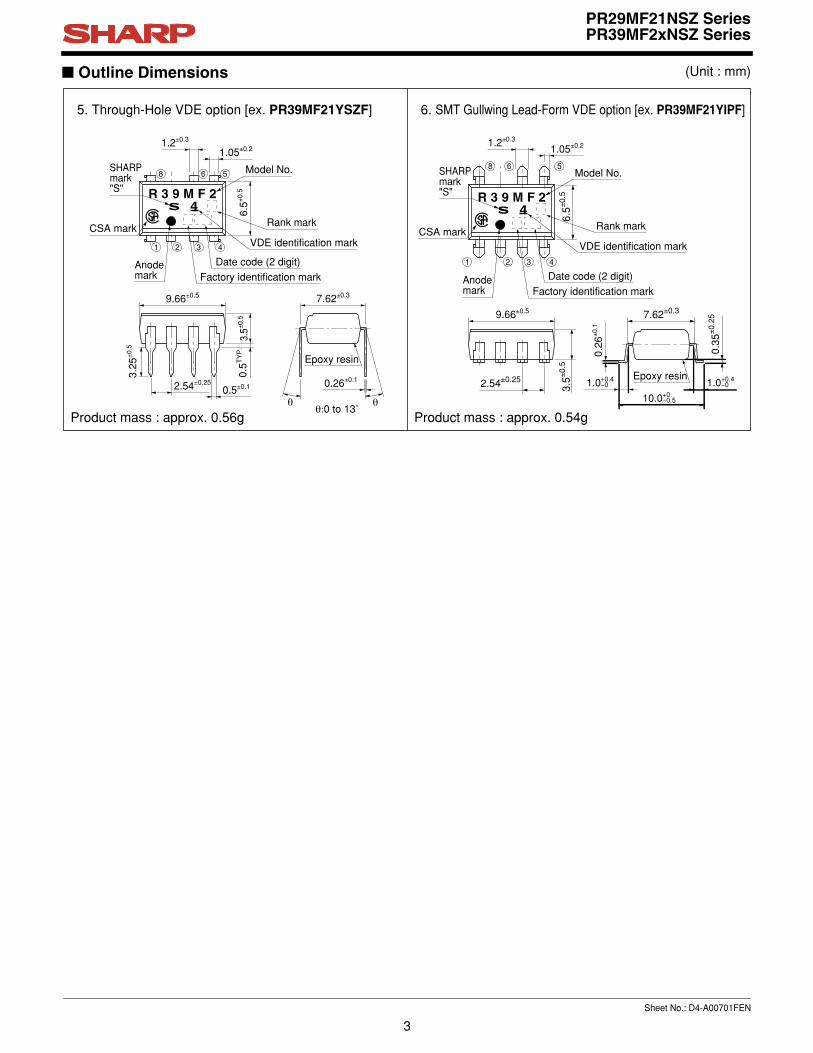
Outline Dimensions (Unit : mm)
1. Through-Hole [ex. PR29MF21NSZF] 2. SMT Gullwing Lead-Form [ex. PR29MF21NIPF]
2.54±0.25
8 6 5
6.5±0
.5
1.05±0.21.2±0.3
9.66±0.5
3.5±0
.5
0.5±0.1
1 2 3 4
3.25
±0.5
0.5T
YP
.
θ θθ:0 to 13˚
7.62±0.3
0.26±0.1
Epoxy resin
R 2 9 M F 2
Anode mark
Date code (2 digit)
Rank mark
Factory identification mark
SHARPmark"S"
CSA mark
Model No. 8 6 5
6.5±0
.52.54±0.25
3.5±0
.51.0+0.4
−0
0.26
±0.1
Epoxy resin
10.0+0−0.5
1.0+0.4−0
0.35
±0.2
57.62±0.39.66±0.5
41 2 3
1.05±0.21.2±0.3
R 2 9 M F 2
Anode mark
Date code (2 digit)
Rank mark
Factory identification mark
SHARPmark"S"
CSA mark
Model No.
3. Through-Hole [ex. PR39MF21NSZF] 4. SMT Gullwing Lead-Form [ex. PR39MF21NIPF]
PR29MF21NSZ SeriesPR39MF2xNSZ Series
Sheet No.: D4-A00701FEN
2.54±0.25
8 6 5
6.5±0
.5
1.05±0.21.2±0.3
9.66±0.5
3.5±0
.5
0.5±0.1
1 2 3 4
3.25
±0.5
0.5T
YP
.
θ θθ:0 to 13˚
7.62±0.3
0.26±0.1
Epoxy resin
R 3 9 M F 2
Anode mark
Date code (2 digit)
Rank mark
Factory identification mark
SHARPmark"S"
CSA mark
Model No. 8
6.5±0
.5
2.54±0.25
3.5±0
.5
1.0+0.4−0
0.26
±0.1
Epoxy resin
10.0+0−0.5
1.0+0.4−0
0.35
±0.2
57.62±0.39.66±0.5
41 2 3
1.05±0.21.2±0.3
6 5
R 3 9 M F 2
Anode mark
Date code (2 digit)
Rank mark
Factory identification mark
SHARPmark"S"
CSA mark
Model No.
Product mass : approx. 0.54gProduct mass : approx. 0.56g
Product mass : approx. 0.54gProduct mass : approx. 0.56g
3
Outline Dimensions (Unit : mm)
5. Through-Hole VDE option [ex. PR39MF21YSZF] 6. SMT Gullwing Lead-Form VDE option [ex. PR39MF21YIPF]
PR29MF21NSZ SeriesPR39MF2xNSZ Series
Sheet No.: D4-A00701FEN
2.54±0.25
8 6 5
6.5±0
.5
1.05±0.21.2±0.3
9.66±0.5
3.5±0
.5
0.5±0.1
1 2 3 4
3.25
±0.5
0.5T
YP
.
θ θθ:0 to 13˚
7.62±0.3
0.26±0.1
Epoxy resin
R 3 9 M F 2
Anode mark
Date code (2 digit)
Rank mark
Factory identification mark
SHARPmark"S"
CSA mark
Model No.
4
VDE identification mark
8
6.5±0
.5
2.54±0.25
3.5±0
.5
1.0+0.4−0
0.26
±0.1
Epoxy resin
10.0+0−0.5
1.0+0.4−0
0.35
±0.2
57.62±0.39.66±0.5
41 2 3
1.05±0.21.2±0.3
6 5
R 3 9 M F 2
Anode mark
Date code (2 digit)
Rank mark
Factory identification mark
SHARPmark"S"
CSA mark
Model No.
4
VDE identification mark
Product mass : approx. 0.54gProduct mass : approx. 0.56g

Date code (2 digit)
Rank markPlease refer to the Model Line-up table.
A.D.
1990
1991
1992
1993
1994
1995
1996
1997
1998
1999
2000
2001
Mark
A
B
C
D
E
F
H
J
K
L
M
N
Mark
P
R
S
T
U
V
W
X
A
B
C
Mark
1
2
3
4
5
6
7
8
9
O
N
D
Month
January
February
March
April
May
June
July
August
September
October
November
December
A.D
2002
2003
2004
2005
2006
2007
2008
2009
2010
2011
2012···
···
2nd digit
Month of production
1st digit
Year of production
Factory identification markFactory identification Mark
no mark
Country of origin
Japan
* This factory marking is for identification purpose only.Please contact the local SHARP sales representative to see the actural status of the production.
4
repeats in a 20 year cycle
PR29MF21NSZ SeriesPR39MF2xNSZ Series
Sheet No.: D4-A00701FEN

Electro-optical CharacteristicsParameter Symbol Unit
Input
Output
(Ta=25˚C)
Forward voltage
Reverse current
Repetitive peak OFF-state current
ON-state voltage
Holding current
Critical rate of rise of OFF-state voltage
Zero cross voltage
Minimum trigger current
Isolation resistance
Turn-on time
Conditions MIN. TYP. MAX.
Transfercharac-teristics
Rank 1Rank 2
Rank 1Rank 2
Rank 1Rank 2
VF
IR
IDRM
VT
IH
dV/dt
VOX
IFT
RISO
ton
V
µA
µA
V
mA
V/µs
V
mA
Ω
µs
IF=20mA
VR=3V
VD=VDRM
IT=0.9A
VD=6V
VD=1/√−2 ·VDRM
IF=15mA, Resistance load
IF=10mA, Resistance load
VD=6V, RL=100Ω
DC500V,40 to 60%RH
IF=20mA, VD=6V, RL=100ΩIF=10mA, VD=6V, RL=100Ω
−
−
−
−
−
100
−
−
−
5×10¹⁰
−
1.2
−
−
−
−
−
−
−
−
1011
−
1.4
10
100
3.0
25
−
35
10
5
−
50
Absolute Maximum Ratings
5
Parameter Symbol Rating Unit
Input
Output
(Ta=25˚C)
Forward current
Reverse voltage
RMS ON-state current
Peak one cycle surge current
Repetitive
peak OFF-state voltage
Isolation voltage
Operating temperature
Storage temperature
Soldering temperature*2
*1
IF
VR
IT(rms)
Isurge
VDRM
Viso(rms)
Topr
Tstg
Tsol
mA
V
A
A
V
kV
˚C
˚C
˚C
*4
*3
*3
*5
50
6
0.9
9
400
600
4.0
−30 to +85
−40 to +125
270*1 40 to 60%RH, AC for 1minute, f=60Hz*2 For 10s*3 Refer to Fig.1, Fig.2*4 f=50Hz sine wave*5 Lead solder plating models: 260˚C
PR29MF21NSZPR39MF2xNSZ
PR29MF21NSZ SeriesPR39MF2xNSZ Series
1mm
Soldering area
Sheet No.: D4-A00701FEN

Lead Form
Shipping Package
DIN
EN60747-5-2
Model No.
Through-Hole
Sleeve
50pcs/sleeve
Taping
1 000pcs/reel
PR39MF22NSZF
SMT Gullwing
PR39MF22NIPF
PR39MF21NSZF
PR39MF22YSZF
PR39MF21YSZF
PR39MF22YIPF
PR39MF21YIPF
- Approved - Approved
IFT[mA](VD=6V,R L=100Ω )
PR29MF21NSZF - PR29MF21NIPF -
Rank mark
MAX.5
MAX.10600
V DRM
[V]
2
1
MAX.10400 1
6
PR29MF21NSZ SeriesPR39MF2xNSZ Series
Sheet No.: D4-A00701FEN
Model Line-up
Please contact a local SHARP sales representative to see the actual status of the production.
PR39MF21NIPF

7
PR29MF21NSZ SeriesPR39MF2xNSZ Series
0
10
20
30
40
50
60
70Fo
rwar
d cu
rren
t IF
(mA
)
Ambient temperature Ta (˚C)
−30 0 50 100
Fig.1 Forward Current vs. Ambient Temperature
Fig.2 RMS ON-state Current vs. Ambient Temperature
Sheet No.: D4-A00701FEN
0
0.2
0.4
0.6
0.8
1
−30 0 50 100
RM
S O
N-s
tate
cur
rent
IT
(rm
s) (
A)
Ambient temperature Ta (˚C)
50
5
1
100
10
0.50 1 1.5 2 2.5 3
−25˚C50˚C
25˚C 0˚C
Forw
ard
curr
ent I
F (m
A)
Forward voltage VF (V)
Ta=75˚C
Fig.3-a Forward Current vs. Forward Voltage (Rank 1)
Fig.4-a Minimum Trigger Current vs. Ambient Temperature (Rank 1)
Fig.3-b Forward Current vs. Forward Voltage (Rank 2)
Fig.4-b Minimum Trigger Current vs. Ambient Temperature (Rank 2)
0
7
6
5
4
3
2
1
Min
imum
trig
ger
curr
ent I
FT (
mA
)
Ambient temperature Ta (°C)
VD=6VRL=100Ω
−30 0 10050
50
5
1
100
10
Forw
ard
curr
ent I
F (m
A)
Forward voltage VF (V)
−25˚C
25˚C 0˚C
Ta=75˚C
50˚C
10.9 1.1 1.2 1.3 1.4 1.5
Min
imum
trig
ger
curr
ent I
FT (
mA
)
Ambient temperature Ta (°C)
−30 0 100500
1
2
3
4
6
5
VD=6VRL=100Ω
8
PR29MF21NSZ SeriesPR39MF2xNSZ Series
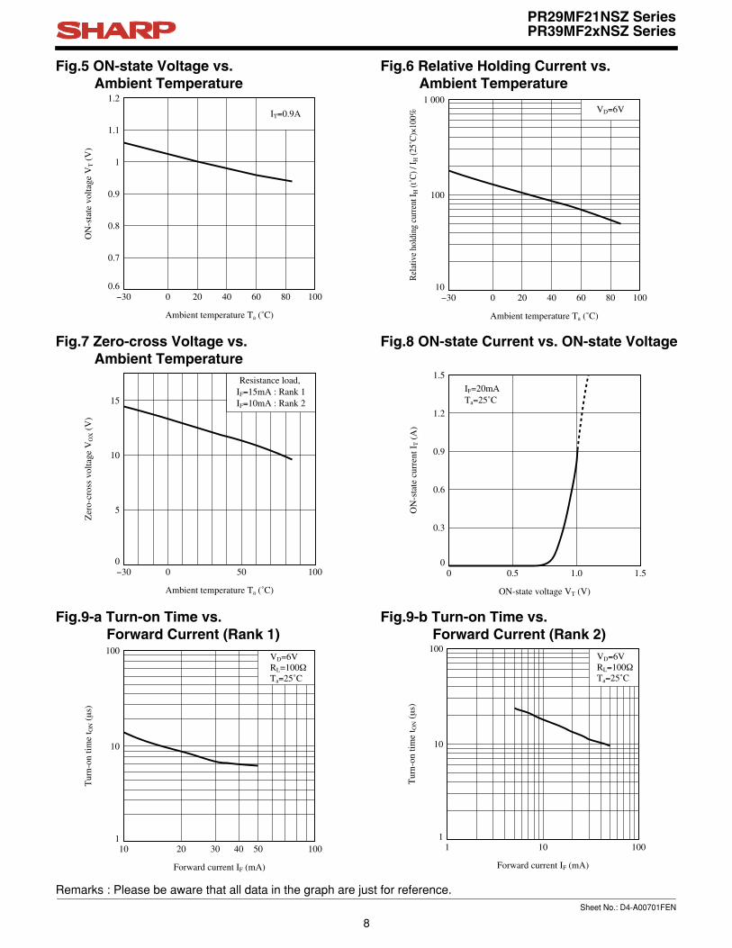
Fig.9-a Turn-on Time vs. Forward Current (Rank 1)
Fig.9-b Turn-on Time vs. Forward Current (Rank 2)
Sheet No.: D4-A00701FEN
Remarks : Please be aware that all data in the graph are just for reference.
Fig.8 ON-state Current vs. ON-state Voltage
100
10
1100
VD=6VRL=100ΩTa=25˚C
10 20 30 40 50
Forward current IF (mA)
Tur
n-on
tim
e t O
N (
µs)
0
0.3
0.6
0.9
1.2
1.5
0 0.5 1.0 1.5
ON
-sta
te c
urre
nt I
T (
A)
ON-state voltage VT (V)
IF=20mATa=25˚C
Fig.7 Zero-cross Voltage vs. Ambient Temperature
0
10
5
15
−30 0 10050
Zer
o-cr
oss
volta
ge V
OX (
V)
Ambient temperature Ta (˚C)
Resistance load, IF=15mA : Rank 1IF=10mA : Rank 2
Fig.5 ON-state Voltage vs. Ambient Temperature
Fig.6 Relative Holding Current vs. Ambient Temperature
0.6
0.8
0.7
1
0.9
1.1
1.2
−30 0 20 40 60 80 100
ON
-sta
te v
olta
ge V
T (
V)
Ambient temperature Ta (˚C)
IT=0.9A
10
100
1 000
−30 0 20 40 60 80 100
Rel
ativ
e ho
ldin
g cu
rren
t IH
(t˚C
) / I H
(25˚
C)×
100%
Ambient temperature Ta (˚C)
VD=6V
100
10
1
VD=6VRL=100ΩTa=25˚C
Forward current IF (mA)
Tur
n-on
tim
e t O
N (
µs)
1001 10

9
PR29MF21NSZ SeriesPR39MF2xNSZ Series
Design Considerations
In order for the SSR to turn off, the triggering current (IF) must be 0.1mA or less.
Particular attention needs to be paid when utilizing SSRs that incorporate zero crossing circuitry.If the phase difference between the voltage and the current at the output pins is large enough, zero crossing type SSRs cannot be used. The result, if zero crossing SSRs are used under this condition, is that the SSR may not turn on and off irregardless of the input current. In this case, only a non zero cross type SSR should be used in combination with the above mentioned snubber circuit selection process.
When the input current (IF) is below 0.1mA, the output Triac will be in the open circuit mode. However, if the voltage across the Triac, VD, increases faster than rated dV/dt, the Triac may turn on. To avoid this situation, please incorporate a snubber circuit. Due to the many different types of load that can be driven, we can merely recommend some circuit values to start with : Cs=0.022µF and Rs=47Ω. The operation of the SSR and snubber circuit should be tested and if unintentional switching occurs, please adjust the snubber circuit component values accordingly.
When making the transition from On to Off state, a snubber circuit should be used ensure that sudden drops in current are not accompanied by large instantaneous changes in voltage across the Triac.This fast change in voltage is brought about by the phase difference between current and voltage.Primarily, this is experienced in driving loads which are inductive such as motors and solenods.Following the procedure outlined above should provide sufficient results.
For over voltage protection, a Varistor may be used.
Any snubber or Varistor used for the above mentioned scenarios should be located as close to the main output triac as possible.
All pins shall be used by soldering on the board. (Socket and others shall not be used.)
DegradationIn general, the emission of the IRED used in SSR will degrade over time.In the case where long term operation and / or constant extreme temperature fluctuations will be applied to the devices, please allow for a worst case scenario of 50% degradation over 5years.Therefore in order to maintain proper operation, a design implementing these SSRs should provide at least twice the minimum required triggering current from initial operation.
Design guide
Sheet No.: D4-A00701FEN
Recommended Operating ConditionsParameter
PR29MF21NSZPR39MF2xNSZ
Symbol Unit
Input
Output
Input signal current
at ON state
Input signal current at OFF state
Load supply voltage
Load supply current
Frequency
Operating temperature
IF(ON)
IF(OFF)
VOUT(rms)
IOUT(rms)
f
Topr
mA
mA
V
mA
Hz
˚C
−
−
−
Locate snubber circuit between output terminals
(Cs=0.022µF, Rs=47Ω)
−
−
Conditions20
10
0
−
−
50
−20
25
15
0.1
120
240
IT(rms)×80%(∗)
60
80
MIN. MAX.
(∗) See Fig.2 about derating curve (IT(rms) vs. ambient temperature).
Rank 1
Rank 2

10
PR29MF21NSZ SeriesPR39MF2xNSZ Series
For additional design assistance, please review our corresponding Optoelectronic Application Notes.
Standard Circuit
Recommended Foot Print (reference)SMT Gullwing Lead-form
2.54
2.54
1.7
2.2
8.2
2.54
(Unit : mm)
Sheet No.: D4-A00701FEN
Tr1
R1
D1
V1
+VCC
AC Line
Load
ZS
ZS : Surge absorption circuit (Snubber circuit)
SSR
82
3 6

Manufacturing Guidelines
Reflow Soldering:Reflow soldering should follow the temperature profile shown below.Soldering should not exceed the curve of temperature profile and time.Please don't solder more than twice.
Soldering Method
Flow Soldering :Flow soldering should be completed below 270˚C and within 10s.Preheating is within the bounds of 100 to 150˚C and 30 to 80s.Please don't solder more than twice.
Hand solderingHand soldering should be completed within 3s when the point of solder iron is below 400˚C.Please don't solder more than twice.
Other noticesPlease test the soldering method in actual condition and make sure the soldering works fine, since the impact on the junction between the device and PCB varies depending on the tooling and soldering conditions.
11
1 2 3 4
300
200
100
00
(˚C)
Terminal : 260˚C peak
( package surface : 250˚C peak)
Preheat
150 to 180˚C, 120s or less
Reflow
220˚C or more, 60s or less
(min)
PR29MF21NSZ SeriesPR39MF2xNSZ Series
Sheet No.: D4-A00701FEN

12
PR29MF21NSZ SeriesPR39MF2xNSZ Series
Sheet No.: D4-A00701FEN
Solvent cleaning :Solvent temperature should be 45˚C or below. Immersion time should be 3minutes or less.
Ultrasonic cleaning :The impact on the device varies depending on the size of the cleaning bath, ultrasonic output, cleaning time, size of PCB and mounting method of the device.Therefore, please make sure the device withstands the ultrasonic cleaning in actual conditions in advance of mass production.
Recommended solvent materials :Ethyl alcohol, Methyl alcohol and Isopropyl alcohol.In case the other type of solvent materials are intended to be used, please make sure they work fine in actual using conditions since some materials may erode the packaging resin.
Cleaning instructions
This product shall not contain the following materials.And they are not used in the production process for this device.Regulation substances : CFCs, Halon, Carbon tetrachloride, 1.1.1-Trichloroethane (Methylchloroform)Specific brominated flame retardants such as the PBBOs and PBBs are not used in this product at all.
Presence of ODC

Package specification
13
12.0
6.7
5.8
10.8
520±2
Sleeve packageThrough-Hole
Package materialsSleeve : HIPS (with anti-static material)Stopper : Styrene-Elastomer
Package methodMAX. 50pcs of products shall be packaged in a sleeve. Both ends shall be closed by tabbed and tabless stoppers.The product shall be arranged in the sleeve with its anode mark on the tabless stopper side.MAX. 20 sleeves in one case.
Sleeve outline dimensions
(Unit : mm)
PR29MF21NSZ SeriesPR39MF2xNSZ Series
Sheet No.: D4-A00701FEN

14
Tape and Reel packageSMT Gullwing
Package materialsCarrier tape : A-PET (with anti-static material) Cover tape : PET (three layer system)Reel : PS
Carrier tape structure and DimensionsF
K
E I
D J
G
B
H
A
C
Dimensions List (Unit : mm)A
16.0±0.3
B
7.5±0.1
C
1.75±0.1
D
12.0±0.1
E
2.0±0.1
H
10.4±0.1
I
0.4±0.05
J
4.2±0.1
K
10.2±0.1
F
4.0±0.1
G
φ1.5+0.1 −0
5˚M
AX
.
H
a
c
e
g
f
b
d
Dimensions List (Unit : mm)a
330
b
17.5±1.5
c
100±1.0
d
13±0.5
e
23±1.0
f
2.0±0.5
g
2.0±0.5
Pull-out direction
[Packing : 1 000pcs/reel]
Reel structure and Dimensions
Direction of product insertion
PR29MF21NSZ SeriesPR39MF2xNSZ Series
Sheet No.: D4-A00701FEN

· The circuit application examples in this publication are provided to explain representative applications of SHARP devices and are not intended to guarantee any circuit design or license any intellectual property rights. SHARP takes no responsibility for any problems rela-ted to any intellectual property right of a third party re-sulting from the use of SHARP's devices.
· Contact SHARP in order to obtain the latest device specification sheets before using any SHARP device. SHARP reserves the right to make changes in the spec-ifications, characteristics, data, materials, structure, and other contents described herein at any time without notice in order to improve design or reliability. Manufac-turing locations are also subject to change without no-tice.
· Observe the following points when using any devices in this publication. SHARP takes no responsibility for damage caused by improper use of the devices which does not meet the conditions and absolute maximum ratings to be used specified in the relevant specification sheet nor meet the following conditions:(i) The devices in this publication are designed for use in general electronic equipment designs such as:
--- Personal computers--- Office automation equipment--- Telecommunication equipment [terminal]--- Test and measurement equipment--- Industrial control--- Audio visual equipment--- Consumer electronics
(ii) Measures such as fail-safe function and redundant design should be taken to ensure reliability and safety when SHARP devices are used for or in connection
with equipment that requires higher reliability such as:--- Transportation control and safety equipment (i.e.,
aircraft, trains, automobiles, etc.)--- Traffic signals--- Gas leakage sensor breakers--- Alarm equipment--- Various safety devices, etc.
(iii) SHARP devices shall not be used for or in connec-tion with equipment that requires an extremely high lev-el of reliability and safety such as:
--- Space applications--- Telecommunication equipment [trunk lines]--- Nuclear power control equipment--- Medical and other life support equipment (e.g.,
scuba).
· If the SHARP devices listed in this publication fall with-in the scope of strategic products described in the For-eign Exchange and Foreign Trade Law of Japan, it is necessary to obtain approval to export such SHARP de-vices.
· This publication is the proprietary product of SHARP and is copyrighted, with all rights reserved. Under the copyright laws, no part of this publication may be repro-duced or transmitted in any form or by any means, elec-tronic or mechanical, for any purpose, in whole or in part, without the express written permission of SHARP. Express written permission is also required before any use of this publication may be made by a third party.
· Contact and consult with a SHARP representative if there are any questions about the contents of this pub-lication.
15
Important Notices
PR29MF21NSZ SeriesPR39MF2xNSZ Series
Sheet No.: D4-A00701FEN