Embed Size (px)
Citation preview
Power splitting ratio couplers based on MMI structures with high
bandwidth and large tolerance using silicon waveguides
Cao-Dung Truong a, Trung-Thanh Le b,*a Hanoi University of Science and Technology, No. 1 Dai Co Viet, Hanoi, Viet Nam
b Hanoi University of Natural Resources and Environment, No. 41A, K1 Road, Phu Dien, Hanoi, Viet Nam
Received 24 November 2012; received in revised form 16 January 2013; accepted 18 January 2013
Available online 26 January 2013
Abstract
We show that it is possible to obtain 2 � 2 couplers based on multimode interference (MMI) structures with nineteen new power-
splitting ratios by cascading three or four MMI couplers. The other aim of this study is to use silicon waveguides, that are compatible
with the existing CMOS (Complementary Metal-Oxide-Semiconductor) fabrication technology, for designing the proposed
devices. The proposed MMI couplers with new power splitting ratios have simple geometries and low losses. These MMI
couplers can offer valuable new possibilities for designing MMI waveguide-based photonic integrated circuits such as all-optical
interconnects, microring resonators, clock distribution, Mach Zehnder Interferometer based on MMI couplers and other all-optical
processing applications. The transfer matrix method (TMM) and modified effective index method (MEIM) along with the support of
the 3D Beam Propagation Method (3D BPM) are used to optimize the proposed devices.
# 2013 Elsevier B.V. All rights reserved.
Keywords: All-optical processing; Integrated optics; Multimode interference (MMI) couplers; Silicon on insulator (SOI); CMOS technology
www.elsevier.com/locate/photonics
Available online at www.sciencedirect.com
Photonics and Nanostructures – Fundamentals and Applications 11 (2013) 217–225
1. Introduction
Multimode interference (MMI) couplers of unequal
power splitting ratios are attractive for photonic
integrated circuit (PICs) applications such as power
taps, high-Q ring resonators [1,2], ladder-structure
optical filters [3] and loop mirror partial reflectors. A
coupler with freely chosen power splitting ratio is
particularly valuable in Mach–Zehnder interferometer
(MZI) structure when loss and gain are asymmetrically
distributed between both different-length arms [4]. In
the literature, it is showed that a conventional MMI
* Corresponding author. Tel.: +84 985 848 193.
E-mail addresses: [email protected],
[email protected] (T.-T. Le).
1569-4410/$ – see front matter # 2013 Elsevier B.V. All rights reserved.
http://dx.doi.org/10.1016/j.photonics.2013.01.002
coupler with a rectangular shape provides only seven
fixed different power splitting ratios [5]. Therefore,
finding a reasonable way for obtaining a variety of
power splitting ratios is particularly important to realize
all-optical signal processing devices based on MMI
couplers [6].
In principle, the way to achieve free choice of power
splitting ratios is to introduce a phase difference at some
special position within the MMI device or between two
couplers in the MZI. The introduction of such a phase
shift will lead to new phase relations between the self-
images at the output plane. Depending on the material
system used for fabricating the MMI couplers, several
approaches have been proposed to obtain arbitrary
power splitting ratios. One of the most commons ways
to ‘‘tune’’ the coupling coefficient of a coupler is to use
an MZI structure [7–9]. The tuning of the refractive
C.-D. Truong, T.-T. Le / Photonics and Nanostructures – Fundamentals and Applications 11 (2013) 217–225218
index using the carrier related plasma effect has been
performed directly within the MMI region. The same
methods can be applied to the devices designed on other
materials but using the thermo-optic effect [10] or
electro-optic [11] to change the refractive index at
special shapes such as butterfly-like MMI, exponential
tapered MMI and angled MMIs to produce a free
selection of the coupling coefficients. The fourth
approach is to use an etching-depth-controlled conven-
tional 2 � 2 MMI [12].
In this paper, we propose a new approach for
achieving MMI couplers with new power splitting ratios
by interconnecting three or four MMI sections together.
The proposed devices can provide nineteen new power
splitting ratios. In addition, in this study silicon
waveguides are used for designing the proposed
devices. An analytical analysis is used to design the
device. Finally, the transfer matrix method (TMM) and
modified effective index method (MEIM) along with
the support of the 3D Beam Propagation Method (3D
BPM) are used to optimize the proposed devices.
2. General theory
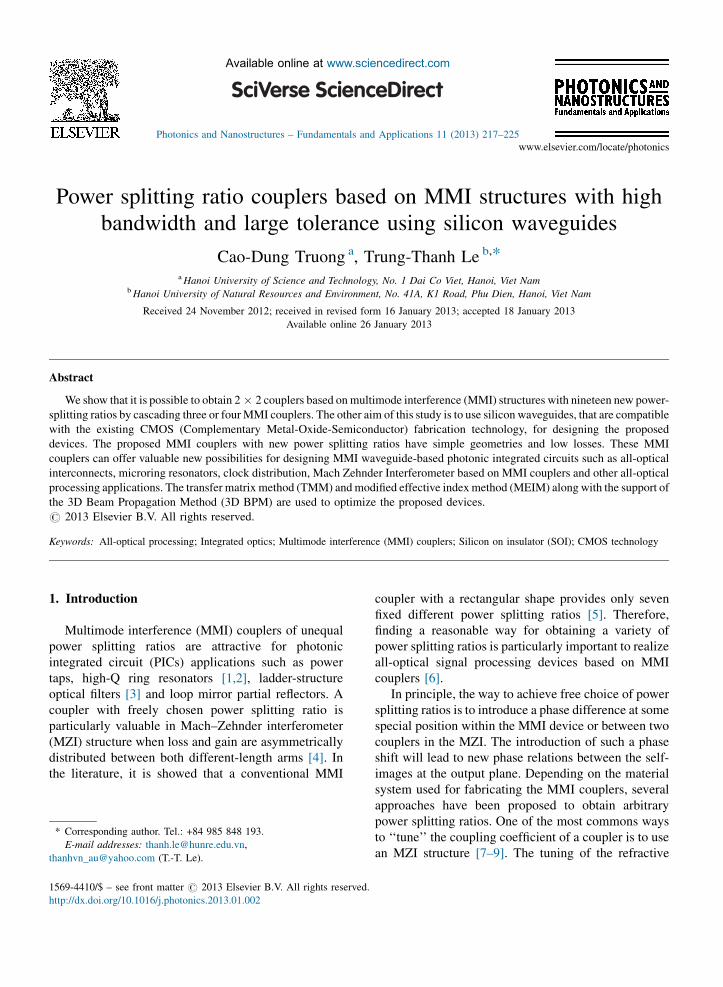
Fig. 1 shows the structure of a single MMI coupler,
where a1 and a2 are the complex amplitudes at two
input ports and b1, b2 are complex amplitudes at two
output ports. The 2 � 2 MMI coupler has a width of
WMMI and a length of LMMI. The width of access
waveguides at input and output ports is assumed to be
Wa. We set s as the distance or separation between two
parallel access waveguides. In order to minimize the
size of the device, separation s is chosen to be small as
possible.
The idea to achieve an MMI coupler with variable
power splitting ratios is to cascade three to four 2 � 2
MMI couplers together. The 2 � 2 MMI couplers have
Fig. 1. Structure of a basic 2 � 2 coupler: (a) inplane view
the same separation s. For an MMI coupler, the beat
length is the most important parameter of an MMI
structure. The beat length Ln between the two lowest
guided modes is given by [1]:
Lp ¼4nsW
2e
3l0
(1)
where l0 is the operating wavelength, ns and nc are the
core refractive index and cladding refractive index,
respectively and We is the effective width of the
MMI coupler that can be expressed by:
We ¼ WMMI þp
l0
ns
nc
� �2s
n2s � n2
c
� ��1=2(2)
where s = 0 for transverse electric (TE) mode and s = 1
for transverse magnetic (TM) mode.
It is well-known that the complex optical field
amplitudes at output ports and input ports of the MMI
coupler are expressed by [7]:
b ¼ Ma (3)
where b = [b1, b2]T, a = [a1, a2]T and M is the transfer
matrix of the 2 � 2 MMI coupler.
In general, the width of the MMI coupler can be
written by WMMI = rs, where r is a constant factor
depending on the multimode interference mechanism
[13,14]. For a single MMI coupler with the rectangular
shape, there have been four coupling coefficients K
(cross-power coupling ratio) corresponding to general
interference and restricted interference mechanisms as
follows [15,16]:
Case A (MMI-A) (K = 0.5, r = 1.44): The transfer
matrix of the MMI coupler in this case is given by:
MA ¼1ffiffiffi2p e� jp=4 e jp=4
e jp=4 e� jp=4
� �(4)
of a 2 � 2 MMI coupler and (b) cross-sectional view.
C.-D. Truong, T.-T. Le / Photonics and Nanostructures – Fundamentals and Applications 11 (2013) 217–225 219
Case B (MMI-B) (K = 0.5, r = 3): The access
waveguides for MMI-B is located exactly at positions
�WMMI/6 from center-line of the multimode wave-
guide. The transfer matrix of the MMI coupler in this
case is given by:
MB ¼1ffiffiffi2p e jp=4 e� jp=4
e� jp=4 e jp=4
� �(5)
Case C (MMI-C) (K = 0.85, r = 2): The access
waveguides in this case is located exactly at positions
�WMMI/4 from the centerline of the multimode
waveguide. The transfer matrix of the MMI coupler
in this case is given by:
MC ¼1ffiffiffi2p
cosð� 3p
8Þe j3p=8 cosð�p
8Þe� jp=8
cosð�p
8Þe� jp=8 cosð� 3p
8Þe j3p=8
0B@
1CA
(6)
Case D (MMI-D) (K = 0.72, r = 2.5): The locations
of access waveguides in this case is at �0.25 s from the
center of the MMI region. The transfer matrix of the
MMI coupler is given by:
MD ¼2ffiffiffi5p
cosð� 3p
10Þe j3p=10 cosð� p
10Þe� j3p=10
cosð� p
10Þe� j3p=10 cosð� 3p
10Þe j3p=10
0B@
1CA(7)
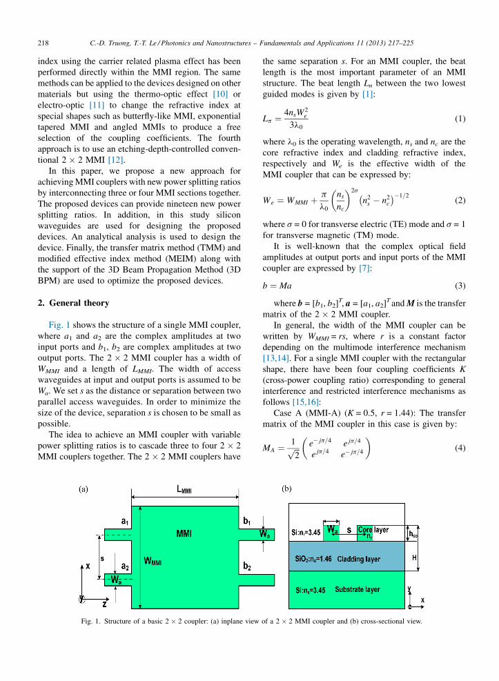
Since four basic MMI sections MMI-A, MMI-B,
MMI-C and MMI-D have the same separation s, they
can be aligned and cascaded to achieve new MMI
structures. In this study, the MMI sections are actually
butt jointed without any interconnecting waveguides.
When MMI-A, MMI-B, MMI-C and MMI-D sections
Fig. 2. Schematic diagram of 2 � 2 MMI coupler based on cascaded 2 � 2
sections.
are cascaded as shown in Fig. 2(a) and (b), the overall
transfer matrix of the cascaded device can be obtained
by:
M ¼ M3M2M1 (8)
M ¼ M4M3M2M1 (9)
where Mi (i = 1, 2, 3, 4) are the transfer matrices of four
MMI sections MMI-A, MMI-B, MMI-C or MMI-D. By
changing properly the positions of the four type MMI
sections A, B, C and D in the configurations of AAD,
ADB, ADCD, BDAD, BDCD, CAD, CDA, CDBD,
CDC, DBD, DCA, DCB, DCD, DDA, DDAD, DDB,
DDBD, DDC, DDCD (Fig. 2), it is possible to achieve
nineteen new power splitting ratios as follows: 0.02,
0.04, 0.084, 0.11, 0.12, 0.16, 0.276, 0.37, 0.38, 0.46,
0.49, 0.54, 0.55, 0.65, 0.73, 0.734, 0.88, 0.91, 0.96.
3. Simulation results and discussion
It is well-known that the three dimensional finite-
difference time-domain (3D-FDTD) method is a
general method to solve Maxwell’s partial differential
equations numerically in the time-domain. Simulation
results for devices based on the silicon waveguide using
3D-FDTD method can achieve a very high accuracy.
However, due to the limitation of computer resource and
memory requirement it is difficult to apply the 3D-
FDTD method to the modeling of large devices on
silicon waveguides. Meanwhile, the BPM was shown to
be a quite suitable method that has sufficient accuracy
for simulating devices based on SOI channel wave-
guides [17,18]. In this paper, we use the BPM along
with the support of the modified effective index method
(MEIM) for designing proposed structure [13]. This
MMI sections: (a) three 2 � 2 MMI sections and (b) four 2 � 2 MMI
C.-D. Truong, T.-T. Le / Photonics and Nanostructures – Fundamentals and Applications 11 (2013) 217–225220
modified effective index method uses beat length Lp as
the invariant. The aim of the MEIM is to find a matching
value of the cladding index for the effective index
method that forces the beat length Lp in the equivalent
2D model (Lp(2D)) to be equal to the beat length in an
accurate 3D model (Lp(3D)). By varying the value of
the cladding refractive index in the 2D model, it is
possible to find an effective cladding index that
produces the same beat length as the accurate 3D
model. The 3D-BPM [19] can be used to compute the
beat length of the 3D waveguide to high accuracy. The
advantage of using the MEIM is that a full 3D solution is
only required once for establishing the matching
cladding index. Then the IEIM can be used to compute
the propagating fields in the MMI structure quickly,
with little further computational effort. Using this
modified effective index method, we found that the
refractive index of the TE fundamental mode is 2.82 at
l0 = 1550 nm in the 2D simulation. In order to match
the low-order modes in the 2D simulation, the
equivalent effective refractive index of the lateral
cladding is calculated to be 2.19 [13].
The waveguide cross-section used in our design is
shown in Fig. 1(b). The core thickness is hco = 220 nm
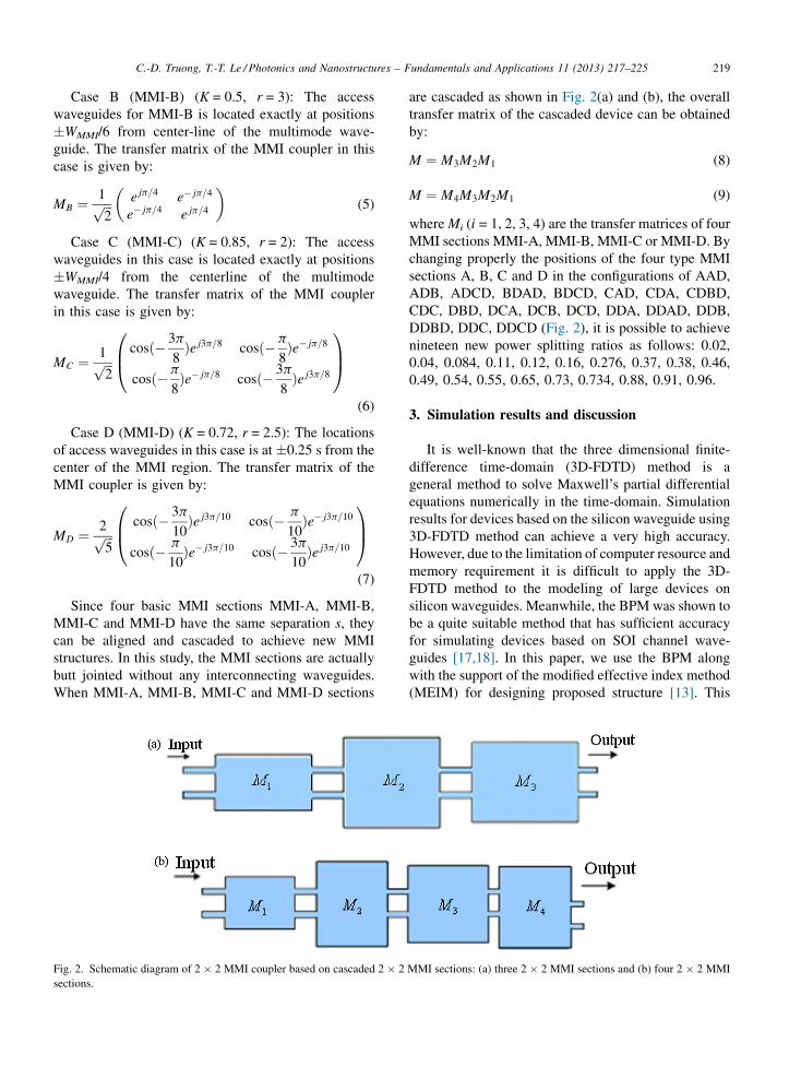
Fig. 3. BPM simulation results of four basic MMI couplers (a) power coupl
lengths.
and the width of the access waveguides is Wa = 500 nm.
In addition, widening the access waveguides improves
the performance of devices. By using the 3D-BPM, it is
found that the access waveguides can be widened via a
taper having a length of Ltp = 5 mm in order to achieve
the lowest loss.
In order to minimize the size of the device, the
separation s is chosen small as possible. This means that
the width of the MMI coupler is large enough to limit
crosstalk between two adjacent parallel waveguides. In
our design, we found that the minimal separation is
chosen to be s = 2.5 mm. First, an analytical method [1]
is used to find the length of the MMI-A, MMI-B, MMI-
C and MMI-D. Then the BPM is used to find optimal
lengths of these MMI couplers.
For the case MMI-A, the width of the MMI-A
coupler is found to be AA = 3.6 mm and the MMI length
LA is found to be LA = (3/2)LpA = 54.72 mm. For the
MMI-B, the width and length of the MMI-B are
WB = 7.5 mm and LB = (1/2)LpB = 73.38 mm, respec-
tively. For the MMI-C, we have the width and length of
WC = 5 mm and LC = (3/4)LpC = 50.68 mm and for the
MMI-D, we have WD = 6.25 mm, MMI length LD = (3/
5)LpD = 62.03 mm. The BPM simulation results are
ing ratios at different lengths and (b) BPM simulations at the optimal
C.-D. Truong, T.-T. Le / Photonics and Nanostructures – Fundamentals and Applications 11 (2013) 217–225 221
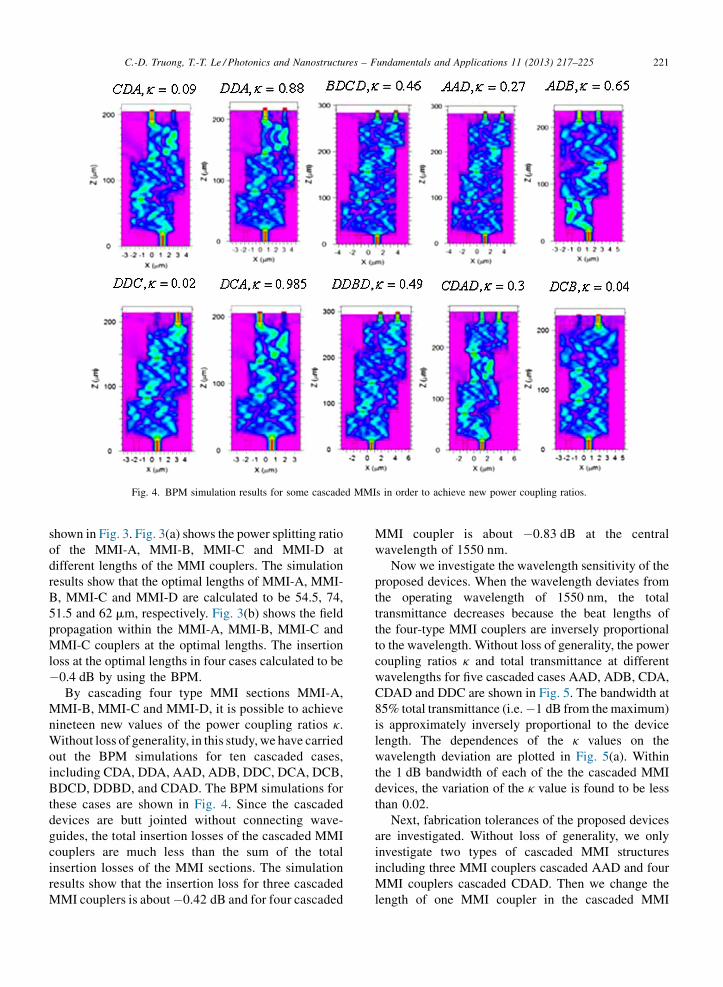
Fig. 4. BPM simulation results for some cascaded MMIs in order to achieve new power coupling ratios.
shown in Fig. 3. Fig. 3(a) shows the power splitting ratio
of the MMI-A, MMI-B, MMI-C and MMI-D at
different lengths of the MMI couplers. The simulation
results show that the optimal lengths of MMI-A, MMI-
B, MMI-C and MMI-D are calculated to be 54.5, 74,
51.5 and 62 mm, respectively. Fig. 3(b) shows the field
propagation within the MMI-A, MMI-B, MMI-C and
MMI-C couplers at the optimal lengths. The insertion
loss at the optimal lengths in four cases calculated to be
�0.4 dB by using the BPM.
By cascading four type MMI sections MMI-A,
MMI-B, MMI-C and MMI-D, it is possible to achieve
nineteen new values of the power coupling ratios k.
Without loss of generality, in this study, we have carried
out the BPM simulations for ten cascaded cases,
including CDA, DDA, AAD, ADB, DDC, DCA, DCB,
BDCD, DDBD, and CDAD. The BPM simulations for
these cases are shown in Fig. 4. Since the cascaded
devices are butt jointed without connecting wave-
guides, the total insertion losses of the cascaded MMI
couplers are much less than the sum of the total
insertion losses of the MMI sections. The simulation
results show that the insertion loss for three cascaded
MMI couplers is about �0.42 dB and for four cascaded
MMI coupler is about �0.83 dB at the central
wavelength of 1550 nm.
Now we investigate the wavelength sensitivity of the
proposed devices. When the wavelength deviates from
the operating wavelength of 1550 nm, the total
transmittance decreases because the beat lengths of
the four-type MMI couplers are inversely proportional
to the wavelength. Without loss of generality, the power
coupling ratios k and total transmittance at different
wavelengths for five cascaded cases AAD, ADB, CDA,
CDAD and DDC are shown in Fig. 5. The bandwidth at
85% total transmittance (i.e. �1 dB from the maximum)
is approximately inversely proportional to the device
length. The dependences of the k values on the
wavelength deviation are plotted in Fig. 5(a). Within
the 1 dB bandwidth of each of the the cascaded MMI
devices, the variation of the k value is found to be less
than 0.02.
Next, fabrication tolerances of the proposed devices
are investigated. Without loss of generality, we only
investigate two types of cascaded MMI structures
including three MMI couplers cascaded AAD and four
MMI couplers cascaded CDAD. Then we change the
length of one MMI coupler in the cascaded MMI
C.-D. Truong, T.-T. Le / Photonics and Nanostructures – Fundamentals and Applications 11 (2013) 217–225222
Fig. 5. (a) The power coupling ratios and (b) total normalized output power of the some cascaded MMI structures at different wavelengths.
structure to obtain the output power. Fig. 6 shows the
BPM simulation results of the output powers of the two
MMI structures at different MMI lengths. Here we
change the length of the type MMI-D coupler. It is
Fig. 6. The power coupling ratio of the three and four cascaded
obvious from the simulations that fabrication tolerances
of both MMI cascaded couplers are very large. The
fabrication tolerance of the MMI lengths for three
cascaded MMI structure is �167 nm for a power
MMI coupler with different lengths of the MMI-D coupler.
C.-D. Truong, T.-T. Le / Photonics and Nanostructures – Fundamentals and Applications 11 (2013) 217–225 223
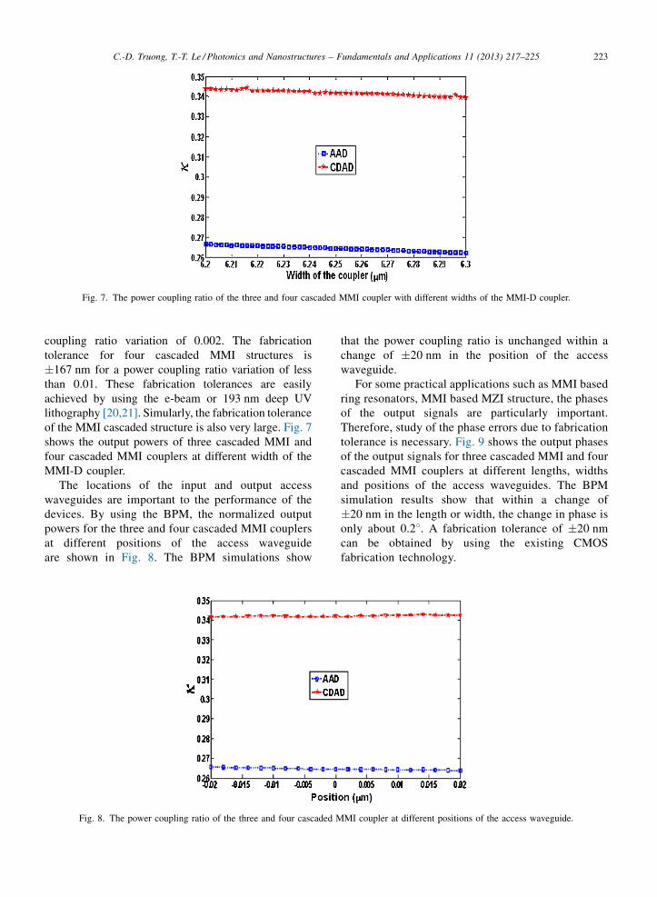
Fig. 7. The power coupling ratio of the three and four cascaded MMI coupler with different widths of the MMI-D coupler.
coupling ratio variation of 0.002. The fabrication
tolerance for four cascaded MMI structures is
�167 nm for a power coupling ratio variation of less
than 0.01. These fabrication tolerances are easily
achieved by using the e-beam or 193 nm deep UV
lithography [20,21]. Simularly, the fabrication tolerance
of the MMI cascaded structure is also very large. Fig. 7
shows the output powers of three cascaded MMI and
four cascaded MMI couplers at different width of the
MMI-D coupler.
The locations of the input and output access
waveguides are important to the performance of the
devices. By using the BPM, the normalized output
powers for the three and four cascaded MMI couplers
at different positions of the access waveguide
are shown in Fig. 8. The BPM simulations show
Fig. 8. The power coupling ratio of the three and four cascaded M
that the power coupling ratio is unchanged within a
change of �20 nm in the position of the access
waveguide.
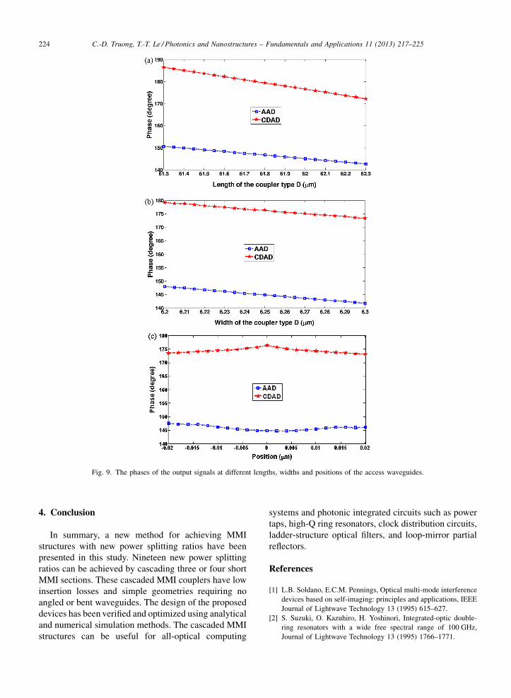
For some practical applications such as MMI based
ring resonators, MMI based MZI structure, the phases
of the output signals are particularly important.
Therefore, study of the phase errors due to fabrication
tolerance is necessary. Fig. 9 shows the output phases
of the output signals for three cascaded MMI and four
cascaded MMI couplers at different lengths, widths
and positions of the access waveguides. The BPM
simulation results show that within a change of
�20 nm in the length or width, the change in phase is
only about 0.28. A fabrication tolerance of �20 nm
can be obtained by using the existing CMOS
fabrication technology.
MI coupler at different positions of the access waveguide.
C.-D. Truong, T.-T. Le / Photonics and Nanostructures – Fundamentals and Applications 11 (2013) 217–225224
Fig. 9. The phases of the output signals at different lengths, widths and positions of the access waveguides.
4. Conclusion
In summary, a new method for achieving MMI
structures with new power splitting ratios have been
presented in this study. Nineteen new power splitting
ratios can be achieved by cascading three or four short
MMI sections. These cascaded MMI couplers have low
insertion losses and simple geometries requiring no
angled or bent waveguides. The design of the proposed
devices has been verified and optimized using analytical
and numerical simulation methods. The cascaded MMI
structures can be useful for all-optical computing
systems and photonic integrated circuits such as power
taps, high-Q ring resonators, clock distribution circuits,
ladder-structure optical filters, and loop-mirror partial
reflectors.
References
[1] L.B. Soldano, E.C.M. Pennings, Optical multi-mode interference
devices based on self-imaging: principles and applications, IEEE
Journal of Lightwave Technology 13 (1995) 615–627.
[2] S. Suzuki, O. Kazuhiro, H. Yoshinori, Integrated-optic double-
ring resonators with a wide free spectral range of 100 GHz,
Journal of Lightwave Technology 13 (1995) 1766–1771.
C.-D. Truong, T.-T. Le / Photonics and Nanostructures – Fundamentals and Applications 11 (2013) 217–225 225
[3] S. Jeong, S. Matsuo, Y. Yoshikuni, et al., Flat-topped spectral
response in a ladder-type interferometric filter, IEICE Transac-
tions on Electronics E88-C (2005) 1747–1754.
[4] P.A. Besse, E. Gini, M. Bachmann, H. Melchior, New 2 � 2 and
1 � 3 multimode interference couplers with free selection of
power splitting ratios, IEEE Journal of Lightwave Technology
14 (1996) 2286–2293.
[5] T.T. Le, L.W. Cahill, D. Elton, The Design of 2 � 2 SOI MMI
couplers with arbitrary power coupling ratios, Electronics Let-
ters 45 (2009) 1118–1119.
[6] Juerg Leuthold, Charles.H. Joyner, Multimode interference cou-
plers with tunable power splitting ratios, IEEE Journal of Light-
wave Technology 19 (2001) pp. 700.
[7] N.S. Lagali, ‘‘The general Mach–Zehnder interferometer using
multimode interference coupler for optical communication net-
work,’’ PhD Thesis: University of Alberta, Canada, 2000.
[8] A. Yariv, Critical coupling and its control in optical waveguide-
ring resonator systems, IEEE Photonics Technology Letters 14
(2002) 483–485.
[9] J.M. Choi, R.K. Lee, A. Yariv, Control of critical coupling in a
ring resonator–fiber configuration: application to wavelength-
selective switching, modulation, amplification, and oscillation,
Optic Letters 26 (2001) 1236–1238.
[10] M. Oguma, K. Jinguji, T. Kitoh, et al., Flat-passband interleave filter
with 200 GHz channel spacing based on planar lightwave circuit-
type lattice structure, Electronics Letters 36 (2000) 1299–1300.
[11] W. Green, R. Lee, G. DeRose, et al., Hybrid InGaAsP-InP Mach–
Zehnder racetrack resonator for thermooptic switching and
coupling control, Optics Express 13 (2005) 1651–1659.
[12] T.T. Le, L.W. Cahill, The design of multimode interference
couplers with arbitrary power splitting ratios on an SOI platform,
in: Presented at LEOS 2008, Newport Beach, California, USA,
2008, November 9–14.
[13] T.T. Le, Multimode Interference Structures for Photonic Signal
Processing, LAP Lambert Academic Publishing, Saarbrucken,
Germany, 2010.
[14] M. Bachmann, P.A. Besse, H. Melchior, Overlapping-image
multimode interference couplers with a reduced number of
self-images for uniform and nonuniform power splitting, Ap-
plied Optics 34 (1995) 6898–6910.
[15] D.J.Y. Feng, P.Y. Chang, T.S. Lay, T.Y. Chang, Novel stepped-
width design concept for compact multimode-interference cou-
plers with low cross-coupling ratio, IEEE Photonics Technology
Letters 19 (2007) 224–226.
[16] David J.Y. Feng, T.S. Lay, T.Y. Chang, Waveguide couplers with
new power splitting ratios made possible by cascading of short
multimode interference sections, Optics Express 15 (2007)
1588–1593.
[17] D. Dai, S. He, Design of an ultrashort Si-nanowaveguide-based
multimode interference coupler of arbitrary shape, Applied
Optics 47 (2008) 38–44.
[18] D. Dai, S. He, Proposal for diminishment of the polarization-
dependency in a Si-nanowire multimode interference (MMI)
coupler by tapering the MMI section, IEEE Photonics Technol-
ogy Letters 20 (2008) 599–601.
[19] N.N. Feng, C. Xu, W.P. Huang, D.G. Fang, A new pre-condi-
tioner based on paraxial approximation for stable and efficient
reflective beam propagation method, IEEE Journal of Lightwave
Technology 21 (2003) 1996–2001.
[20] W. Bogaerts, P. Dumon, D. Taillaert, et al., SOI nanophotonic
waveguide structures fabricated with deep UV lithography,
Photonics and Nanostructures – Fundamentals and Applications
2 (2004) 81–86.
[21] W. Bogaerts, R. Baets, P. Dumon, et al., Nanophotonic wave-
guides in silicon-on-insulator fabricated with CMOS technology,
IEEE Journal of Lightwave Technology 23 (2005) 401–412.


![PROCEEDINGS OF SPIE · 9450 0V Bi-directional triplexer with butterfly MMI coupler using SU-8 polymer waveguides [9450-104] 9450 0W Micro-optical insertion system for WDM transceiver](https://img.pdfslide.us/doc/110x75/5f4b1c532266e369e97e6ef6/proceedings-of-spie-9450-0v-bi-directional-triplexer-with-butterfly-mmi-coupler.jpg)