Embed Size (px)
Citation preview
University of Technology Lecture Note 2 Electrical Engineering Department Introduction to PSDs Electrical Engineering Division Page 1 of 10 EG 405: Power Electronics Dr. Oday A. Ahmed
Power semiconductor devices Power semiconductor devices constitute the heart of modern power electronic apparatus. The main function of the power semiconductor devices (PSD) in the power converter system are used as on/off switches to control the energy transfer between the source and the load. The Basic representation of the power semiconductor device can be represented as a traditional switch as shown in Fig.1.
Fig.1
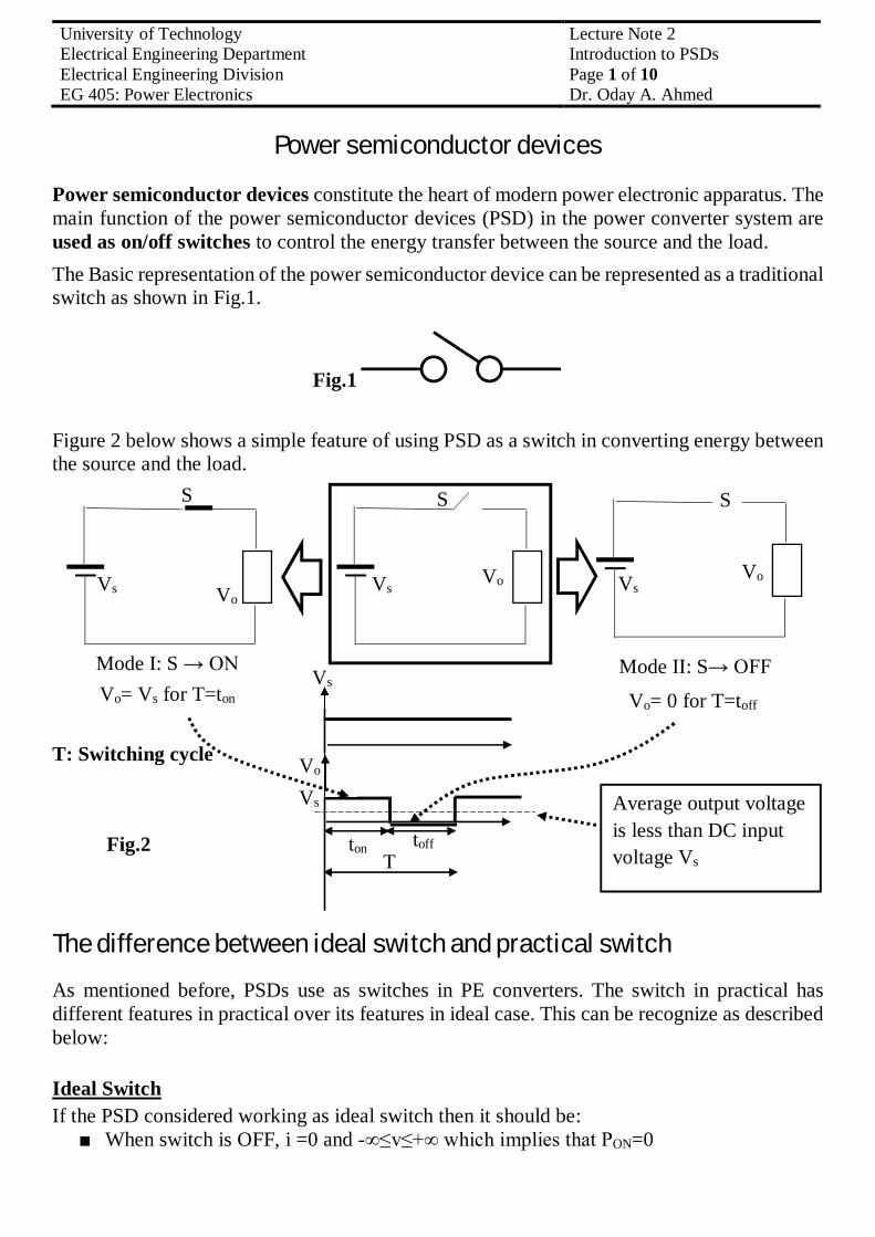
Figure 2 below shows a simple feature of using PSD as a switch in converting energy between the source and the load.
T: Switching cycle
The difference between ideal switch and practical switch As mentioned before, PSDs use as switches in PE converters. The switch in practical has different features in practical over its features in ideal case. This can be recognize as described below: Ideal Switch If the PSD considered working as ideal switch then it should be:
■ When switch is OFF, i =0 and -∞≤v≤+∞ which implies that PON=0
Vs
S
Vo Vo
Vs
Mode I: S → ON
Vo= Vs for T=ton
Vs Vo
Mode II: S→ OFF
Vo= 0 for T=toff
Vs
ton toff
Vo
Average output voltage is less than DC input voltage Vs
Vs
Fig.2
S S
T
University of Technology Lecture Note 2 Electrical Engineering Department Introduction to PSDs Electrical Engineering Division Page 2 of 10 EG 405: Power Electronics Dr. Oday A. Ahmed
■ When switch is ON, V =0 and -∞≤ I ≤+∞ which implies that PON=0
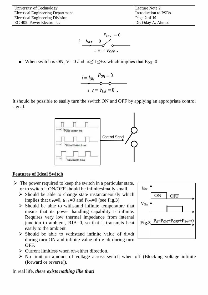
It should be possible to easily turn the switch ON and OFF by applying an appropriate control signal.
Features of Ideal Switch
The power required to keep the switch in a particular state, or to switch it ON/OFF should be infinitesimally small. Should be able to change state instantaneously which
implies that tON=0, tOFF=0 and PSW=0 (see Fig.3) Should be able to withstand infinite temperature that
means that its power handling capability is infinite. Requires very low thermal impedance from internal junction to ambient, RJA=0, so that it transmits heat easily to the ambient
Should be able to withstand infinite value of di=dt during turn ON and infinite value of dv=dt during turn OFF.
Current limitless when on-either direction. No limit on amount of voltage across switch when off (Blocking voltage infinite
(forward or reverse)).
In real life, there exists nothing like that!
Control Signal
Fig.3
University of Technology Lecture Note 2 Electrical Engineering Department Introduction to PSDs Electrical Engineering Division Page 3 of 10 EG 405: Power Electronics Dr. Oday A. Ahmed
Practical Switch
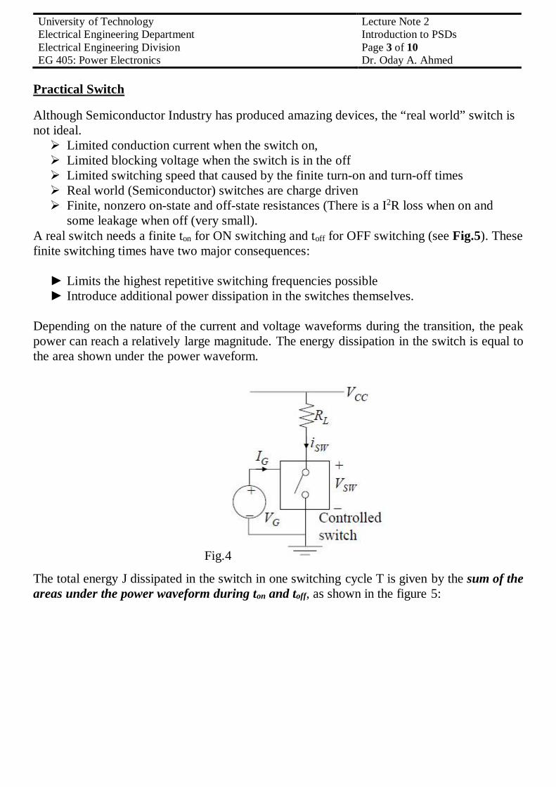
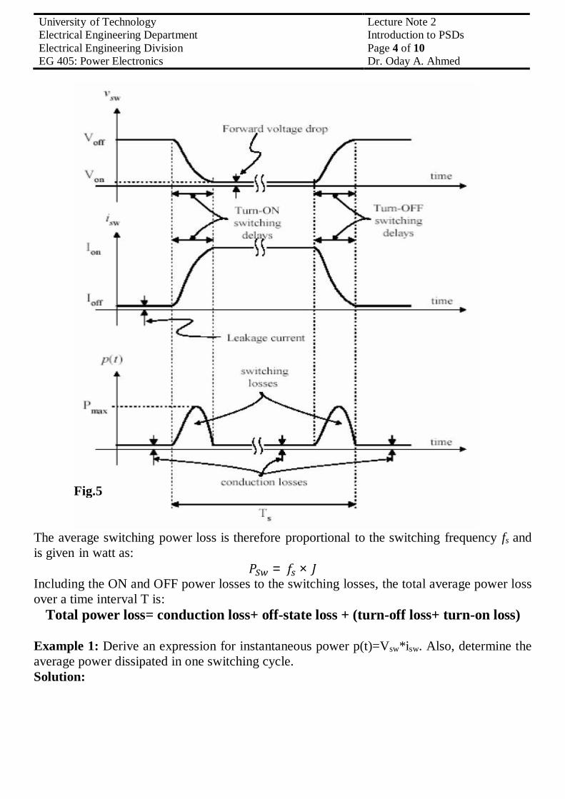
Although Semiconductor Industry has produced amazing devices, the “real world” switch is not ideal. Limited conduction current when the switch on, Limited blocking voltage when the switch is in the off Limited switching speed that caused by the finite turn-on and turn-off times Real world (Semiconductor) switches are charge driven Finite, nonzero on-state and off-state resistances (There is a I2R loss when on and
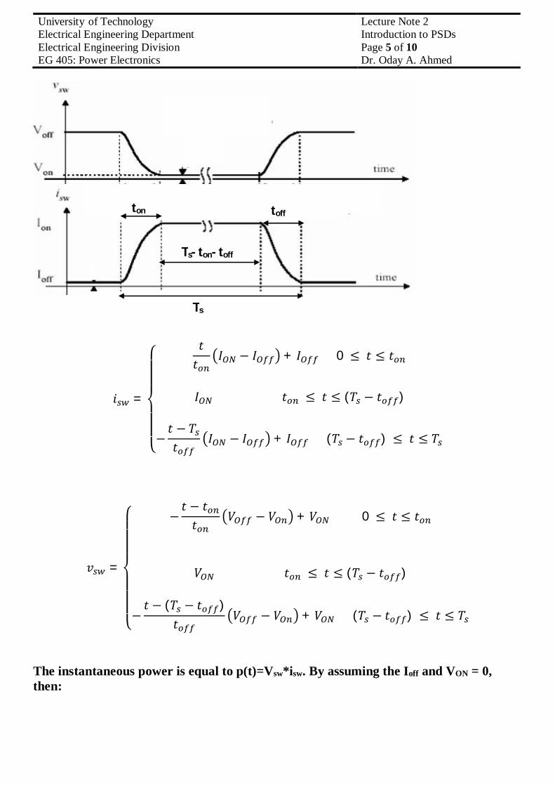
some leakage when off (very small). A real switch needs a finite ton for ON switching and toff for OFF switching (see Fig.5). These finite switching times have two major consequences:
► Limits the highest repetitive switching frequencies possible ► Introduce additional power dissipation in the switches themselves.
Depending on the nature of the current and voltage waveforms during the transition, the peak power can reach a relatively large magnitude. The energy dissipation in the switch is equal to the area shown under the power waveform.
Fig.4
The total energy J dissipated in the switch in one switching cycle T is given by the sum of the areas under the power waveform during ton and toff, as shown in the figure 5:
University of Technology Lecture Note 2 Electrical Engineering Department Introduction to PSDs Electrical Engineering Division Page 4 of 10 EG 405: Power Electronics Dr. Oday A. Ahmed
The average switching power loss is therefore proportional to the switching frequency fs and is given in watt as:
푃 = 푓 × 퐽 Including the ON and OFF power losses to the switching losses, the total average power loss over a time interval T is:
Total power loss= conduction loss+ off-state loss + (turn-off loss+ turn-on loss) Example 1: Derive an expression for instantaneous power p(t)=Vsw*isw. Also, determine the average power dissipated in one switching cycle. Solution:
Fig.5
University of Technology Lecture Note 2 Electrical Engineering Department Introduction to PSDs Electrical Engineering Division Page 5 of 10 EG 405: Power Electronics Dr. Oday A. Ahmed
푖 =
⎩⎪⎪⎨
⎪⎪⎧
푡푡
퐼 − 퐼 + 퐼 0 ≤ 푡 ≤ 푡
퐼 푡 ≤ 푡 ≤ (푇 − 푡 )
−푡 − 푇푡
퐼 − 퐼 + 퐼 (푇 − 푡 ) ≤ 푡 ≤ 푇
푣 =
⎩⎪⎪⎪⎨
⎪⎪⎪⎧ −
푡 − 푡푡
푉 − 푉 + 푉 0 ≤ 푡 ≤ 푡
푉 푡 ≤ 푡 ≤ (푇 − 푡 )
−푡 − (푇 − 푡 )
푡푉 − 푉 + 푉 (푇 − 푡 ) ≤ 푡 ≤ 푇
The instantaneous power is equal to p(t)=Vsw*isw. By assuming the Ioff and VON = 0, then:
Ts
ton toff
Ts- ton- toff
University of Technology Lecture Note 2 Electrical Engineering Department Introduction to PSDs Electrical Engineering Division Page 6 of 10 EG 405: Power Electronics Dr. Oday A. Ahmed
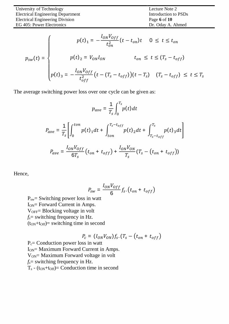
푝 (푡) =
⎩⎪⎪⎨
⎪⎪⎧ 푝(푡) = −
퐼 푉푡
(푡 − 푡 )푡 0 ≤ 푡 ≤ 푡
푝(푡) = 푉 퐼 푡 ≤ 푡 ≤ (푇 − 푡 )
푝(푡) = −퐼 푉푡
푡 − (푇 − 푡 ) (푡 − 푇 ) (푇 − 푡 ) ≤ 푡 ≤ 푇
The average switching power loss over one cycle can be given as:
푝 =1푇
푝(푡)푑푡
푃 =1푇
푝(푡) 푑푡 + 푝(푡) 푑푡 + 푝(푡) 푑푡
푃 =퐼 푉
6푇푡 + 푡 +
퐼 푉푇
(푇 − 푡 + 푡 )
Hence,
푃 =퐼 푉
6푓 . 푡 + 푡
Psw= Switching power loss in watt ION= Forward Current in Amps. VOFF= Blocking voltage in volt fs= switching frequency in Hz. (tON+tOff)= switching time in second
푃 = (퐼 푉 )푓 . (푇 − 푡 + 푡 Pc= Conduction power loss in watt ION= Maximum Forward Current in Amps. VON= Maximum Forward voltage in volt fs= switching frequency in Hz. Ts - (tON+tOff)= Conduction time in second
University of Technology Lecture Note 2 Electrical Engineering Department Introduction to PSDs Electrical Engineering Division Page 7 of 10 EG 405: Power Electronics Dr. Oday A. Ahmed
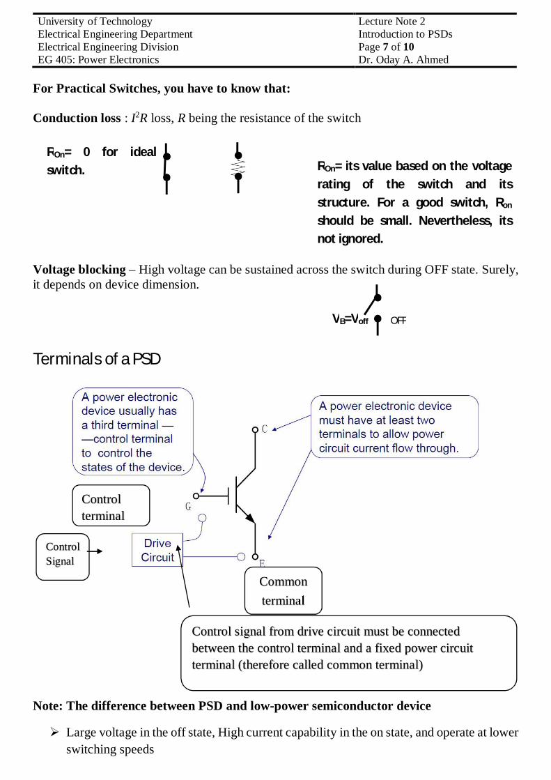
For Practical Switches, you have to know that: Conduction loss : I2R loss, R being the resistance of the switch
Voltage blocking – High voltage can be sustained across the switch during OFF state. Surely, it depends on device dimension.
Terminals of a PSD
Note: The difference between PSD and low-power semiconductor device
Large voltage in the off state, High current capability in the on state, and operate at lower switching speeds
ROn= its value based on the voltage rating of the switch and its structure. For a good switch, Ron should be small. Nevertheless, its not ignored.
ROn= 0 for ideal switch.
OFF VB=Voff
Control signal from drive circuit must be connected between the control terminal and a fixed power circuit terminal (therefore called common terminal)
Control terminal
Common terminal
Control Signal
University of Technology Lecture Note 2 Electrical Engineering Department Introduction to PSDs Electrical Engineering Division Page 8 of 10 EG 405: Power Electronics Dr. Oday A. Ahmed
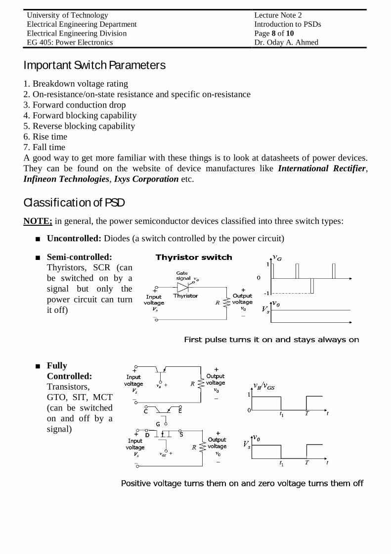
Important Switch Parameters 1. Breakdown voltage rating 2. On-resistance/on-state resistance and specific on-resistance 3. Forward conduction drop 4. Forward blocking capability 5. Reverse blocking capability 6. Rise time 7. Fall time A good way to get more familiar with these things is to look at datasheets of power devices. They can be found on the website of device manufactures like International Rectifier, Infineon Technologies, Ixys Corporation etc. Classification of PSD NOTE; in general, the power semiconductor devices classified into three switch types:
■ Uncontrolled: Diodes (a switch controlled by the power circuit)
■ Semi-controlled: Thyristors, SCR (can be switched on by a signal but only the power circuit can turn it off)
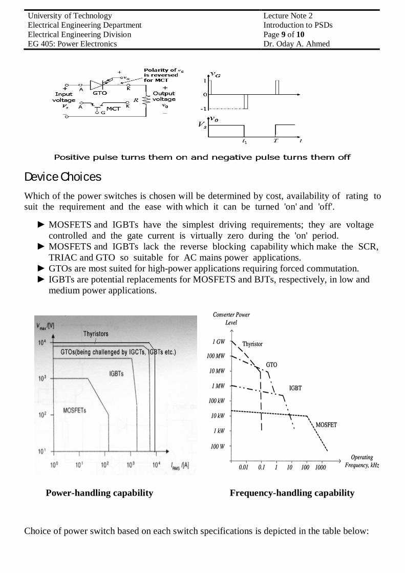
■ Fully Controlled: Transistors, GTO, SIT, MCT (can be switched on and off by a signal)
University of Technology Lecture Note 2 Electrical Engineering Department Introduction to PSDs Electrical Engineering Division Page 9 of 10 EG 405: Power Electronics Dr. Oday A. Ahmed
Device Choices Which of the power switches is chosen will be determined by cost, availability of rating to suit the requirement and the ease with which it can be turned 'on' and 'off'.
► MOSFETS and IGBTs have the simplest driving requirements; they are voltage controlled and the gate current is virtually zero during the 'on' period.
► MOSFETS and IGBTs lack the reverse blocking capability which make the SCR, TRIAC and GTO so suitable for AC mains power applications.
► GTOs are most suited for high-power applications requiring forced commutation. ► IGBTs are potential replacements for MOSFETS and BJTs, respectively, in low and
medium power applications.
Power-handling capability Frequency-handling capability
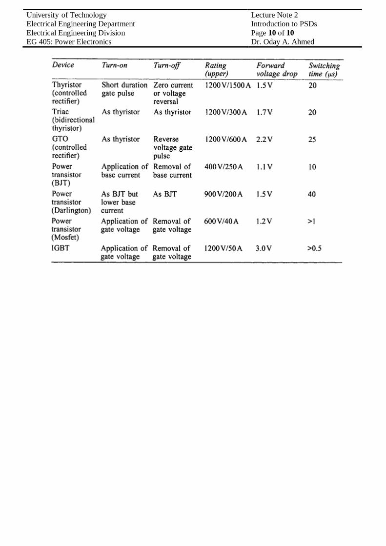
Choice of power switch based on each switch specifications is depicted in the table below:
University of Technology Lecture Note 2 Electrical Engineering Department Introduction to PSDs Electrical Engineering Division Page 10 of 10 EG 405: Power Electronics Dr. Oday A. Ahmed