Embed Size (px)
Citation preview

FACULDADE DE ENGENHARIA DA UNIVERSIDADE DO PORTO
Power reduction of a CMOS high-speedinterface using power gating
Luís Miguel Granja Gomes
FOR JURY EVALUATION
Mestrado Integrado em Engenharia Eletrotécnica e de Computadores
FEUP Supervisor: Prof. João Canas Ferreira
Synopsys Supervisor: Engineer Hélder Araújo
June 25, 2013

c© Luís Gomes, 2013

Resumo
A indústria de circuitos VLSI sofreu uma série de revoluções na forma como os chips eletrónicossão projetados. Começou com o uso de linguagens de descrição de hardware e de avançadasferramentas de trabalho, com o objetivo de diminuir os tempos de projeto e de produção, aomesmo tempo que circuitos mais rápidos e pequenos eram construídos. A produção de dispos-itivos eletrónicos aumentou significativamente, de tal modo que, hoje, são usados biliões todos osdias.
Atualmente, o maior desafio não é só projetar circuitos integrados mais pequenos e rápidos, masmanter esses acréscimos de velocidade e diminuição de tamanho, reduzindo simultaneamente oconsumo de potência. Com a diminuição do tamanho da tecnologia e o uso de transístores comtensões de threshold cada vez mais reduzidas, o consumo de potência dinâmica e estática atingiuníveis insuportáveis. Chegou-se a um ponto em que, tanto económica como ambientalmente fa-lando, é obrigatório projetar para reduzir a potência.
Synopsys, uma das maiores empresas desta indústria, apresentou um projeto com o objetivo deimplementar Power Gating numa das suas interfaces de alta velocidade, como técnica mais eficazna redução da potência estática.
Esta dissertação apresenta as adaptações necessárias para a implementação de Power Gating us-ando ferramentas Synopsys, aplicando-as a um caso de estudo complexo. Os conceitos principaise o fluxo normal de projeto são introduzidos. Depois, para cada etapa e respetiva ferramenta,explicam-se a estratégia e metodologia utilizadas para implementar Power Gating na interfacealvo. Consideram-se ambas as etapas de implementação e verificação.
O uso do UPF (Unified Power Format) revela-se a melhor forma de descrever as características dealimentação de um projeto de baixo consumo, e é descrito como este é interpretado pelas diversasferramentas EDA.
Nas etapas backend explica-se a utilização de células especiais para controlar a alimentação docircuio e, assim, reduzir as correntes de fuga associadas ao consumo de potência estática. Na fasede verificação mostra-se a utilização das complexas ferramentas na presença de Power Gating.Consideram-se as principais métricas, restrições e implicações existentes numa implementaçãodesta técnica.
Os resultados finais são apresentados, tendo em conta o impacto na área, queda de tensão, desem-penho, funcionalidade e consumo de potência. Como resultado final, atinge-se uma redução doconsumo estático de até 99.5%.
i

ii

Abstract
The VLSI industry has undergone a series of revolutions in the way chips are designed. It startedwith the use of HDL languages and advanced tools to improve time-to-market and produce fasterand smaller chips. The production of those chips increased significantly to a point where billionsof electronic devices are used every day.
Now, the biggest challenge isn’t only designing faster and smaller chips, but to keep these im-provements in speed and size while reducing power consumption. With technology scaling downand smaller threshold voltages being used, switching and leakage power became unbearably high,to a point where economically and environmentally speaking, it is mandatory to design for lowpower.
Synopsys, one of the biggest companies in this industry, proposed a project with the objective ofimplementing Power Gating, as one of the most effective leakage reduction techniques, in a state-of-the-art high-speed interface.
This dissertation presents the adaptations required to implement power gating using Synopsystools and applies them to a complex case study. It starts with an introduction of the main conceptsinvolved, followed by the presentation of the standard design flow. Then, for each flow stage andrespective tool, the methodology used to power gate the target interface is depicted, respecting agiven strategy. Both, implementation and verification stages are addressed.
UPF (Unified Power Format) power intent specification is used to inform EDA tools, across theentire flow, about the characteristics of a low power design.
In the backend stages, it is shown how to insert power switches and how to use them to reduceleakage power. In the verification stages it is explained how to use the complex verification tools,considering a power gated design. The main metrics and challenges are explained, as well as theconstraints and implications associated with the implementation of this low power technique.
The final results are presented showing the impact in area, IR-drop, performance, functionalityand power consumption. The outcome is a decrease of leakage power of up to 99.5%.
iii

iv

Acknowledgements
I would like to address my deepest gratitude...
To my supervisor João Canas Ferreira, for all his availability, suggestions and experience.
To my Synopsys supervisor Hélder Araújo for all his support, knowledge transfer and great lead-ership.
To Sérgio Costa for all his patience, expertise and help in the developed work.
To Mara Carvalho and Luís Cruz for all the help and knowledge.
To Nelson Silva and Miguel Oliveira for all the discussions regarding this dissertation and for thecomradeship during its development.
To Synopsys for giving me the opportunity of developing this dissertation. To Synopsys team forhaving received me as one of their own.
To my parents and sister, the persons that made all this academic path possible, made me who Iam and always have supported me. Without you, this moment would not be possible, thus thisdissertation is dedicated to you.
To the rest of my family, who didn’t let me stop working hard.
To Filipa for all the friendship, happiness, motivation, and especially for being my biggest support.
To BEST and all his members for such great moments and for having taught me so much. To PortoCompetitions Team, Ju, Ninja and Júlio.
To all my friends and comrades for all the incredible moments, knowledge sharing, motivation andfor making everything easier in the worst moments.
Finally, to FEUP and all my Professors.
Luís Gomes
v

vi

“if it wasn’t hard they wouldn’t call it hardware”
J.F. Wakerly
vii

viii

Contents
1 Introduction 11.1 Context . . . . . . . . . . . . . . . . . . . . . . . . . . . . . . . . . . . . . . . 21.2 Motivation and Goals . . . . . . . . . . . . . . . . . . . . . . . . . . . . . . . . 21.3 Structure of the document . . . . . . . . . . . . . . . . . . . . . . . . . . . . . . 3
2 Background 52.1 Energy vs Power . . . . . . . . . . . . . . . . . . . . . . . . . . . . . . . . . . 52.2 Dynamic and Static Power . . . . . . . . . . . . . . . . . . . . . . . . . . . . . 6
2.2.1 Dynamic Power . . . . . . . . . . . . . . . . . . . . . . . . . . . . . . . 62.2.2 Static Power . . . . . . . . . . . . . . . . . . . . . . . . . . . . . . . . 7
2.3 Power Gating Overview . . . . . . . . . . . . . . . . . . . . . . . . . . . . . . . 82.4 Power Gating Challenges . . . . . . . . . . . . . . . . . . . . . . . . . . . . . . 10
2.4.1 Voltage Island identification . . . . . . . . . . . . . . . . . . . . . . . . 112.4.2 Wake-Up Time, In-Rush Current and Power/Ground Bounce . . . . . . . 112.4.3 Power Switching Fabric . . . . . . . . . . . . . . . . . . . . . . . . . . 122.4.4 Retention Registers . . . . . . . . . . . . . . . . . . . . . . . . . . . . . 162.4.5 Isolation Cells . . . . . . . . . . . . . . . . . . . . . . . . . . . . . . . 17
3 Interface and Project Requirements 193.1 SNPS high-speed interface . . . . . . . . . . . . . . . . . . . . . . . . . . . . . 19
3.1.1 Physical and Power Consumption data . . . . . . . . . . . . . . . . . . . 203.2 Project Requirements . . . . . . . . . . . . . . . . . . . . . . . . . . . . . . . . 21
4 Standard design flow 234.1 Front End Flow . . . . . . . . . . . . . . . . . . . . . . . . . . . . . . . . . . . 234.2 Backend flow . . . . . . . . . . . . . . . . . . . . . . . . . . . . . . . . . . . . 25
4.2.1 Synthesis . . . . . . . . . . . . . . . . . . . . . . . . . . . . . . . . . . 264.2.2 Synthesis Verification . . . . . . . . . . . . . . . . . . . . . . . . . . . 264.2.3 Place&Route . . . . . . . . . . . . . . . . . . . . . . . . . . . . . . . . 274.2.4 Parasitic extraction . . . . . . . . . . . . . . . . . . . . . . . . . . . . . 314.2.5 Static Timing Analysis (STA) . . . . . . . . . . . . . . . . . . . . . . . 314.2.6 Post-layout Analysis and Verification . . . . . . . . . . . . . . . . . . . 314.2.7 Integration and DRC/LVS Verification . . . . . . . . . . . . . . . . . . . 32
4.3 Summary . . . . . . . . . . . . . . . . . . . . . . . . . . . . . . . . . . . . . . 32
5 Low Power Design Flow 335.1 Power Intent Specification using UPF . . . . . . . . . . . . . . . . . . . . . . . 33
5.1.1 UPF Concepts . . . . . . . . . . . . . . . . . . . . . . . . . . . . . . . 33
ix

x CONTENTS
5.2 Low Power Flow Using Synopsys Tools . . . . . . . . . . . . . . . . . . . . . . 345.3 Summary . . . . . . . . . . . . . . . . . . . . . . . . . . . . . . . . . . . . . . 35
6 Power Gating Implementation 376.1 Power Gating Strategy . . . . . . . . . . . . . . . . . . . . . . . . . . . . . . . 376.2 Frontend stage . . . . . . . . . . . . . . . . . . . . . . . . . . . . . . . . . . . . 376.3 Describing the power intent using UPF . . . . . . . . . . . . . . . . . . . . . . . 386.4 Synthesis using Design Compiler . . . . . . . . . . . . . . . . . . . . . . . . . . 426.5 Formal Verification using Formality . . . . . . . . . . . . . . . . . . . . . . . . 426.6 Floorplan Modification using Custom Designer . . . . . . . . . . . . . . . . . . 436.7 Library Data Preparation . . . . . . . . . . . . . . . . . . . . . . . . . . . . . . 43
6.7.1 Libraries . . . . . . . . . . . . . . . . . . . . . . . . . . . . . . . . . . 456.7.2 Libraries creation . . . . . . . . . . . . . . . . . . . . . . . . . . . . . . 46
6.8 Technology File and Metal Layers . . . . . . . . . . . . . . . . . . . . . . . . . 466.9 Adding supply (PG) pins around rxlanedig . . . . . . . . . . . . . . . . . . . . . 476.10 Place&Route using IC Compiler . . . . . . . . . . . . . . . . . . . . . . . . . . 486.11 STA with PrimeTime . . . . . . . . . . . . . . . . . . . . . . . . . . . . . . . . 576.12 Rail Analysis with Prime Rail and ICC . . . . . . . . . . . . . . . . . . . . . . . 596.13 Power Analysis with PrimeTime PX . . . . . . . . . . . . . . . . . . . . . . . . 616.14 Integration and LVS/DRC checking . . . . . . . . . . . . . . . . . . . . . . . . 62
7 Results 657.1 IR Drop Analysis . . . . . . . . . . . . . . . . . . . . . . . . . . . . . . . . . . 65
7.1.1 Comparative Analysis . . . . . . . . . . . . . . . . . . . . . . . . . . . 657.1.2 Final Results . . . . . . . . . . . . . . . . . . . . . . . . . . . . . . . . 67
7.2 In-Rush Current and Wake-Up Time . . . . . . . . . . . . . . . . . . . . . . . . 707.3 Area overhead . . . . . . . . . . . . . . . . . . . . . . . . . . . . . . . . . . . . 727.4 Functionality and Performance Impact . . . . . . . . . . . . . . . . . . . . . . . 72
7.4.1 Post-layout simulation . . . . . . . . . . . . . . . . . . . . . . . . . . . 727.4.2 STA with IR-drop induced delay . . . . . . . . . . . . . . . . . . . . . . 737.4.3 Co-simulation . . . . . . . . . . . . . . . . . . . . . . . . . . . . . . . . 75
7.5 Power Consumption . . . . . . . . . . . . . . . . . . . . . . . . . . . . . . . . . 75
8 Conclusion 818.1 Final Conclusions . . . . . . . . . . . . . . . . . . . . . . . . . . . . . . . . . . 818.2 Future Work . . . . . . . . . . . . . . . . . . . . . . . . . . . . . . . . . . . . . 83
A UPF specification for the FC 85
B STA Reports for FC 89B.1 STA report discarding IR-Drop . . . . . . . . . . . . . . . . . . . . . . . . . . . 89B.2 STA report considering IR-Drop . . . . . . . . . . . . . . . . . . . . . . . . . . 91
C STA Reports for SC 95C.1 STA report discarding IR-Drop . . . . . . . . . . . . . . . . . . . . . . . . . . . 95C.2 STA report considering IR-Drop . . . . . . . . . . . . . . . . . . . . . . . . . . 98
References 103

List of Figures
1.1 Leakage Power increase as predicted by ITRS [1] . . . . . . . . . . . . . . . . 3
2.1 Switching Power sources. Source: [2] . . . . . . . . . . . . . . . . . . . . . . . 62.2 Short Power sources. Source: [2] . . . . . . . . . . . . . . . . . . . . . . . . . 72.3 Leakage Power sources. Source: [2] . . . . . . . . . . . . . . . . . . . . . . . 82.4 Power gating concept. Source: [3] . . . . . . . . . . . . . . . . . . . . . . . . 92.5 Logic blocks controlled by power switches. Source: [4] . . . . . . . . . . . . . 102.6 Elements in a power gating implementation. Source: [3] . . . . . . . . . . . . . 112.7 Fine grained implementation of an AND gate. Source: [3] . . . . . . . . . . . . 132.8 Coarse grained implementation. Source: [5] . . . . . . . . . . . . . . . . . . . 142.9 Header (left) and Footer (right) power switches. Source: [3] . . . . . . . . . . . 152.10 Ring implementation. Source: [3] . . . . . . . . . . . . . . . . . . . . . . . . . 162.11 Array implementation. Source: [3] . . . . . . . . . . . . . . . . . . . . . . . . 172.12 Retention register. Source: [3] . . . . . . . . . . . . . . . . . . . . . . . . . . . 18
3.1 PHYGNRX blocks diagram . . . . . . . . . . . . . . . . . . . . . . . . . . . . 213.2 PHYGNRX supply connections . . . . . . . . . . . . . . . . . . . . . . . . . . 22
4.1 Frontend design flow. . . . . . . . . . . . . . . . . . . . . . . . . . . . . . . . . 244.2 Backend design flow and related Synopsys tools. . . . . . . . . . . . . . . . . . 254.3 Synthesis as done by DC. . . . . . . . . . . . . . . . . . . . . . . . . . . . . . . 27
5.1 Low power design flow using Synopsys tools. Adapted from: [2] . . . . . . . . 35
6.1 Blocks diagram of the modified design. . . . . . . . . . . . . . . . . . . . . . . 386.2 UPF diagram. . . . . . . . . . . . . . . . . . . . . . . . . . . . . . . . . . . . . 396.3 Original floorplan. . . . . . . . . . . . . . . . . . . . . . . . . . . . . . . . . . . 436.4 Modified floorplan. . . . . . . . . . . . . . . . . . . . . . . . . . . . . . . . . . 446.5 Added pins on the floorplan boundary . . . . . . . . . . . . . . . . . . . . . . . . 446.6 Library Preparation flow . . . . . . . . . . . . . . . . . . . . . . . . . . . . . . 476.7 Added PG pins . . . . . . . . . . . . . . . . . . . . . . . . . . . . . . . . . . . 486.8 ICC Flow for a Power Gating Implementation. Main stages highlighted in purple 496.9 Ring with 260 power switches . . . . . . . . . . . . . . . . . . . . . . . . . . . 546.10 Power switches connected in a daisy-chain fashion . . . . . . . . . . . . . . . . 556.11 Metal 7 power straps placed on top of the power switches . . . . . . . . . . . . . 566.12 Final layout in ICC . . . . . . . . . . . . . . . . . . . . . . . . . . . . . . . . . 576.13 In Design Rail Analysis Flow . . . . . . . . . . . . . . . . . . . . . . . . . . . . 606.14 Final layout integrated using Custom Designer . . . . . . . . . . . . . . . . . . . 63
xi

xii LIST OF FIGURES
7.1 IR-drop over net VP considering 260 power switching cells . . . . . . . . . . . . 667.2 IR-drop imposed by the 260 power switching cells . . . . . . . . . . . . . . . . 677.3 IR-drop over net VP considering 518 power switching cells . . . . . . . . . . . . 687.4 IR-drop over net VPS_DIG considering 518 power switching cells . . . . . . . . 697.5 IR-drop imposed by the 518 power switching cells . . . . . . . . . . . . . . . . 707.6 In-Rush Current and Wake-Up Time for a FC analysis . . . . . . . . . . . . . . . 737.7 In-Rush Current versus the sum of all current sources . . . . . . . . . . . . . . . 747.8 Post-layout simulation waveforms . . . . . . . . . . . . . . . . . . . . . . . . . 747.9 Co-simulation for power gating validation . . . . . . . . . . . . . . . . . . . . . 767.10 Co-simulation and wake-up time . . . . . . . . . . . . . . . . . . . . . . . . . . 777.11 Co-simulation for the FC . . . . . . . . . . . . . . . . . . . . . . . . . . . . . . 787.12 Co-simulation for the SC . . . . . . . . . . . . . . . . . . . . . . . . . . . . . . 79

List of Tables
3.1 Maximum clock frequency of each operating mode . . . . . . . . . . . . . . . . 203.2 Supply Voltages . . . . . . . . . . . . . . . . . . . . . . . . . . . . . . . . . . . 203.3 Physical data . . . . . . . . . . . . . . . . . . . . . . . . . . . . . . . . . . . . 223.4 Power consumption fot the FC . . . . . . . . . . . . . . . . . . . . . . . . . . . 223.5 Power consumption fot the TYPC . . . . . . . . . . . . . . . . . . . . . . . . . 223.6 Power consumption for the SC . . . . . . . . . . . . . . . . . . . . . . . . . . . 22
6.1 Metal layers routing directions . . . . . . . . . . . . . . . . . . . . . . . . . . . 476.2 Power switching cells characteristics . . . . . . . . . . . . . . . . . . . . . . . . 516.3 Multiplexer delays for the three corners . . . . . . . . . . . . . . . . . . . . . . 59
7.1 IR-drop values with 260 power switching cells (FC) . . . . . . . . . . . . . . . . 657.2 IR-drop and rise values with 518 power switching cells (FC) . . . . . . . . . . . 677.3 IR-drop and rise values with 518 power switching cells (TYP) . . . . . . . . . . 707.4 IR-drop and rise values with 518 power switching cells (SC) . . . . . . . . . . . 717.5 IR-drop across the power switching cells . . . . . . . . . . . . . . . . . . . . . . 717.6 In-Rush Current and Wake-Up Time . . . . . . . . . . . . . . . . . . . . . . . . 727.7 Area and cell number results . . . . . . . . . . . . . . . . . . . . . . . . . . . . 727.8 IR-drop induced delay for a timing path (setup analysis) . . . . . . . . . . . . . . 757.9 Leakage Power Consumption and savings . . . . . . . . . . . . . . . . . . . . . 767.10 Leakage Power by elements . . . . . . . . . . . . . . . . . . . . . . . . . . . . 787.11 Power Impact in HS-mode . . . . . . . . . . . . . . . . . . . . . . . . . . . . . 797.12 Power Impact in LS-mode . . . . . . . . . . . . . . . . . . . . . . . . . . . . . 80
xiii

xiv LIST OF TABLES

Abreviations
AFE Analogue Front EndALU Arithmetic Logic UnitBVP Blockage Via PinCCS Composite Current SourceCDL Circuit Description LanguageCMOS Complementary Metal–Oxide–SemiconductorCTS Clock Tree SynthesisDC Design CompilerDRC Design Rules CheckDUT Device Under TestEDA Electronic Design AutomationEM ElectromigrationFC Fast CornerFEUP Faculdade de Engenharia da Universidade do PortoFSM Finite State MachineGDSII Graphic Database System IIGTECH General TechnologyGUI Graphical User InterfaceHDL Hardware Description LanguagesHS High-speedIC Integrated CircuitICC IC CompilerIEEE Institute of Electrical and Electronics EngineersIO Input and OutputIP Intellectual PropertyLEF Library Exchange FormatLS Low-speedLVS Layout versus SchematicNMOS N-type metal-oxide-semiconductorPG Power and GroundPMOS p-type metal-oxide-semiconductorPNS Power Network SynthesisPST Power State TablePVT Process, Voltage and TemperatureRC Resistance and CapacitanceRTL Register Transfer LevelRX ReceiverSAIF Switching Activity Interchange Format
xv

xvi LIST OF TABLES
SBPF Synopsys Binary Parasitic FormatSC Slow CornerSDF Standard Delay FormatSPEF Standard Parasitic Exchange FormatSoC System-On-A-ChipSPEF Standard Parasitic Exchange FormatSTA Static Timing AnalysisTYPC Typical CornerTX TransmitterUPF Unified Power FormatVCD Value Change DumpVLSI Very Large Scale Integration

Chapter 1
Introduction
In modern life, we are facing an evergrowing expansion of electronic devices. A normal day of
an ordinary person is strongly associated with the use of equipments that makes life easier. For
instance, it is possible to carry around and watch films in a small and high resolution tablet, which
has a battery life of several hours. It is undeniable that electronic equipments have a strong impact
in many distinct areas, such as medicine or entertainment.
This expansion was possible due to a series of revolutions in the way electronic companies
produce VLSI circuits. To address the growth in chip density, HDL languages started to be used.
More recently, for big designs, writing the full RTL description is no longer feasible or profitable,
as it represents huge design teams or/and a longer time-to-market. This way, design reuse and IP
emerged as a new design trend and as a new revolution. More importantly, the use of EDA tools
enhanced the automation of design and production of chips.
As a result chips are becoming smaller and faster and now what is possible to achieve with
electronic devices is, undoubtedly, incredible. However, as technology scaled down into the sub-
micron era and higher levels of integration are used, a new problem arise. The power consumption
of a digital chip increased to a level where its reduction has become one of the biggest challenges
of digital design.
In the sub-micron technologies, from 90nm and below, leakage current, that once was ne-
glected, is becoming a big slice of the total power consumption. Designers are adopting several
techniques to reduce both dynamic and leakeage power consumption. Among the most used, it is
possible to distinguish Clock Gating, Power Gating, Multi VDD or Multi Vt.
In this dissertation Power Gating is applied to a Synopsys high-speed interface in order to
mitigate its leakage current. The entire design flow is covered from backend to a low power
physical implementation. It is also, presented the modifications that need to be made to a standard
design flow.
The target audience of this document are persons already familiarized with VLSI design that
are interested in a real implementation of power gating using Synopsys tools.
1

2 Introduction
1.1 Context
This MSc Dissertation was developed as part of the Master in Electrical and Computers Engi-
neering of the Faculty of Engineering of the University of Porto (FEUP). It was proposed by and
developed on SNPS Portugal Lda.
It emerged from the need of reducing the power consumption of a state-of-the-art Synopsys Inc
high-speed interface, while, at the same time, studying the more efficient way of using Synopsys
EDA tools in order to implement power gating.
SNPS Portugal Lda office is located at Maia (Portugal) and it is one of the ofices of Synopsys
Inc. Synopsys Inc (Nasdaq:SNPS) is a world leader in electronic design automation and semicon-
ductor intellectual property. The company is headquartered in Mountain View, California, and has
approximately 80 offices located throughout North America, Europe, Japan, Asia and India.
1.2 Motivation and Goals
The main concerns of CMOS VLSI design were timing and area. Power was not much of a concern
since CMOS was considered a low power technology.
The already mentioned technology scaling and the consequent growth in chip integration and
clock speeds led to a significant increase in power and temperature density. A point was reached
were designing for low power was a must. Portable devices run on battery, which makes every
power saving vital. On the other hand, circuits noise immunity decrease and cooling and packaging
costs increase. For instance, and as refered by [6], in 2006, the United States of America server
farms consumed about 61TWh, wich represented a cost of 4.5 billion dollars on cooling systems.
The sheer cost of the electrical energy is, itself an motivation for low power designs. Reducing the
power consumption of a small, but with a large scale utilization, IP block can result in cost savings
and even reduce the environmental footprint.
In the beginning of the low power design revolution, the main concern was on controlling the
dynamic power. The more efficient strategy was to decrease the supply voltage, which, in turn, has
a quadratic impact in the dynamic power, as latter shown in Chapter 2. However, to compensate
the loss in performance, driven by lower supply voltages, transistors with lower threshold voltages
started to be used. This, of course led to higher leakage current and, consequently, higher leakage
power consumption. This fact turned impossible to continue dropping the supply voltage, which
is now halted at around 1V [3]. It is, then, important to also control leakage. ITRS predicted
that leakage current would increase 8 times from 2007 to 2015 (Figure 1.1) [1]. On the other
hand, the evolution and the increasing utilization of high-speed interfaces, such as the one that is
the subject on this dissertation, made leakage power a bigger part of the total power consumption
of a digital circuit. Their operation tend to be bursty, which means that there are short periods of
switching activity, interleaved with long periods of idle state, where leakage is dominant.
Power Gating is an aggressive and the most effective leakage power reduction technique. It is
simple to understand that, the more time the circuit is powered off, the less energy it consumes.

1.3 Structure of the document 3
Figure 1.1: Leakage Power increase as predicted by ITRS [1]
As important as understanding the need to reduce the power consumption and, in particular,
the leakage power, is to know how to instruct EDA tools on how to do so and follow a design flow
that allows the best results.
As so, this dissertation has the following particular goals:
• Reduce the power consumption of a Synopsys high speed interface;
• Preserve the interface functionality;
• Understand how to use Synopsys EDA tools to implement Power Gating using the best
design flow
1.3 Structure of the document
The structure of the document is as follows. Chapter 2 presents the background concepts regarding
a power gating implementation, which is the result of a literature review. Chapter 3 presents the
target high-speed interface. Chapter 4 depicts the the standard design flow, which needs to be
adapted for power gating. The adapted low power flow is presented in a high-level perspective in
Chapter 5. Chapter 6 describes the implementation itself, while explaining the low-level power
gating methodology for each flow stage and tool. The conducted analyses and verifications, as
well as the results are shown in Chapter 7. Finally, 8 presents the final conclusions and future
work suggestion.

4 Introduction

Chapter 2
Background
This chapter summarizes a literature review on the main concepts involved in a low power design,
in particular a power gating implementation. First, the concepts regarding power consumption
and the different types of power dissipation are addressed. Then, the power gating concept is
explained, along with the main challenges of its implementation.
2.1 Energy vs Power
Regarding a project which goal is to reduce the power consumption of a system, it is important to
distinguish these two concepts, many times confused.
When referring to power, we are considering the instantaneous power present in the circuit. It
is defined as the product of the current that flows through its terminals by the voltage at the same
terminals, as shown by Equation 2.1.
P(t) =V (t)× I(t) (2.1)
In turn, the energy consumed by the circuit over a certain interval of time is defined as the
integral of the power. In other words it is the area under the power curve, as shown by Equation
2.2.
E =∫ T
0P(t)dt. (2.2)
Finally the expression of the average power over a time interval is represented in Equation
2.3.
Pavg =ET
=1T
∫ T
0P(t)dt. (2.3)
5

6 Background
Figure 2.1: Switching Power sources. Source: [2]
The operating state of an electronic device has direct reflexes in the instantaneous power. If we
consider a mobile phone, receiving a call implies more power than the standby mode. This way,
the bigger the instantaneous power, the bigger the energy consumed and, therefore, the battery life
decreases.
2.2 Dynamic and Static Power
In the power gating context, it is the static (or leakage) power that deserves more attention. How-
ever, it is interesting to understand from where does the total power consumption of a circuit comes
from. According to Equation 2.4, it is the sum of two components, dynamic and static power, are
depicted in the following sections.
Ptot = Pdin +Pstat (2.4)
2.2.1 Dynamic Power
Dynamic power is the result of the circuit switching activity (reflected in the charge and discharge
of the capacities that compose the circuit) and the short-circuit current that arises when both PMOS
and NMOS network are conducting, as illustrated in Figure 2.1.
Pdyn = Pswitch +Pshort (2.5)
Supposing that the circuit has an effective capacitance of all the nodes CL, is powered with a
supply voltage VDD and is operating with a clock frequency of fclk, Pswitch can be defined as
Pswitch =V 2DD ∗CL ∗ fclk ∗α (2.6)
where α represents an activity factor, which is the transition from 0 to 1 probability.

2.2 Dynamic and Static Power 7
Figure 2.2: Short Power sources. Source: [2]
Pshort is the result of short periods of time (T ) when both PMOS and NMOS networks are
conducting, leading to the creation of a crowbar current (Ishort), as illustrated in Figure 2.2.
Pshort =VDD ∗ Ishort ∗T ∗ fclk (2.7)
In this context, as long as the transition time isn’t to long, Pshort remains small compared with
Pswitch.
2.2.2 Static Power
Static Power is present even when the switching activity is zero and it is not dependent on the
clock frequency. It is associated with leakage currents that exist since the circuit is powered on.
As so, it is many times referred as Leakage Power. Until the 90nm node technology, leakage
power was almost neglected compared with dynamic power. However, as introduced in Chapter
1, with technology scaling down, as we began using processes with low threshold voltages and
thin gate oxides, leakage became a big part of the total power consumption [7]. Leakage currents
have different sources, as shown in Figure 2.3. [6] explains each one as follows:
• Sub-threshold leakage: Isub is the current that flows from the drain to the source of the
transistor when it is in the weak inversion region, which means that Vgs <Vt . Using common
words, it is the current that flows through the transistor when it was supposed to be off;
• Gate leakage - Once it is isolated by a dielectric, the current through a MOS transistor gate
is, ideally zero. However, there is a current Igate that flows directly from the gate to the body,
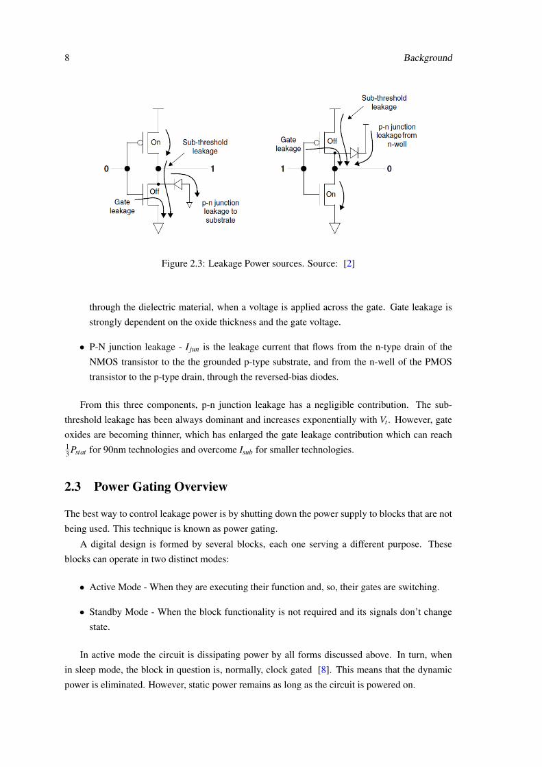
8 Background
Figure 2.3: Leakage Power sources. Source: [2]
through the dielectric material, when a voltage is applied across the gate. Gate leakage is
strongly dependent on the oxide thickness and the gate voltage.
• P-N junction leakage - I jun is the leakage current that flows from the n-type drain of the
NMOS transistor to the the grounded p-type substrate, and from the n-well of the PMOS
transistor to the p-type drain, through the reversed-bias diodes.
From this three components, p-n junction leakage has a negligible contribution. The sub-
threshold leakage has been always dominant and increases exponentially with Vt . However, gate
oxides are becoming thinner, which has enlarged the gate leakage contribution which can reach13 Pstat for 90nm technologies and overcome Isub for smaller technologies.
2.3 Power Gating Overview
The best way to control leakage power is by shutting down the power supply to blocks that are not
being used. This technique is known as power gating.
A digital design is formed by several blocks, each one serving a different purpose. These
blocks can operate in two distinct modes:
• Active Mode - When they are executing their function and, so, their gates are switching.
• Standby Mode - When the block functionality is not required and its signals don’t change
state.
In active mode the circuit is dissipating power by all forms discussed above. In turn, when
in sleep mode, the block in question is, normally, clock gated [8]. This means that the dynamic
power is eliminated. However, static power remains as long as the circuit is powered on.

2.3 Power Gating Overview 9
Figure 2.4: Power gating concept. Source: [3]
Power gating consists on switching off the power supply from blocks that are in standby mode
and switching the power back on when their functionality is required.
Figure 2.4 illustrates the power gating concept. The SLEEP event triggers power gating,
switching power off, while the WAKE event switches power back on. At this time, it is possible
to say that the Standby Mode has became a Sleep Mode, where leakage is reduced.
In order to switch power off, high Vt transistors are are used as switches and placed between the
block PG (power and ground) pins and the PG rails, as illustrated in Figure 2.5. These transistors
can be called Power Switches and two types are considered:
• Header Switch - PMOS transistor placed between the power pins and the power rails;
• Footer switch - NMOS transistor placed between the ground pins and the ground rails;
This way the controlled block, is no longer powered by the main power rails (always-on rails),
but by a switched/virtual power rail. The control of the power switches is achieved through an
enable or sleep signal. For an header switch, the enable signal takes the logic value 1 in order to
switch power off. In the footer switch case, the opposite happens. This signal can be produced by
a power gating controller FSM or it can, simply, be an input port of the design.
As important as the power switches themselves is to distribute and deliver power in the best
way possible across the whole design. The power network should be designed to minimize the
voltage drop and to correctly power all blocks and standard cells in the design.
Additionally, a state retention strategy can be implemented. Depending on the application, it
can be necessary to save the state of the block. This way, when power is switched back on, the
block can return to the exact same functioning state. This is achieved by using state retention
registers. It may be also important to isolate the powered-off block output signals. These signals,
if floating, can induce a crow-bar current in an adjacent block, to which represent input signals.
With this objective, isolation cells can be used.
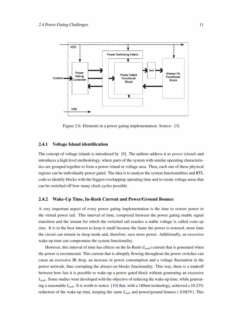
As described above, a power gating implementation contains the following elements:

10 Background
Figure 2.5: Logic blocks controlled by power switches. Source: [4]
• Power switching fabric
• Control Signal or Power Gating Controller FSM
• Power network
• Retention registers (additionally)
• Isolation cells (additionally)
Figure 2.6 shows the power gating elements and their connections.
2.4 Power Gating Challenges
The elements described in Section 2.3 are the backbone of a power gating implementation. Along
with its design, there are several issues that need to be taken into account [3]
• Voltage areas identification;
• IR drop imposed by the power switches and by the power network;
• In-Rush current through the power switches generated when the circuit is powered on and
consequent power dissipation;
• The wake-up time;
• The amount of leakage introduced by the power switches and other power gating related
cells;
• Performing state-dependent and power transition verification.
2.4 Power Gating Challenges 11
Figure 2.6: Elements in a power gating implementation. Source: [3]
2.4.1 Voltage Island identification
The concept of voltage islands is introduced by [9]. The authors address it as power islands and
introduces a high level methodology, where parts of the system with similar operating characteris-
tics are grouped together to form a power island or voltage area. Then, each one of these physical
regions can be individually power gated. The idea is to analyse the system functionalities and RTL
code to identify blocks with the biggest overlapping operating time and to create voltage areas that
can be switched off how many clock cycles possible.
2.4.2 Wake-Up Time, In-Rush Current and Power/Ground Bounce
A very important aspect of every power gating implementation is the time to restore power to
the virtual power rail. This interval of time, comprised between the power gating enable signal
transition and the instant for which the switched rail reaches a stable voltage is called wake-up
time. It is in the best interest to keep it small because the faster the power is restored, more time
the circuit can remain in sleep mode and, therefore, save more power. Additionally, an excessive
wake-up time can compromise the system functionality.
However, this interval of time has effects on the In-Rush (Irush) current that is generated when
the power is reconnected. This current that is abruptly flowing throughout the power switches can
cause an excessive IR drop, an increase in power consumption and a voltage fluctuation in the
power network, thus corrupting the always-on blocks functionality. This way, there is a tradeoff
between how fast it is possible to wake-up a power gated block without generating an excessive
Irush. Some studies were developed with the objective of reducing the wake-up time, while generat-
ing a reasonable Irush. It is worth to notice [10] that, with a 180nm technology, achieved a 10.23%
reduction of the wake-up time, keeping the same Irush and power/ground bounce ( 0.083V). This

12 Background
outcome is a result of activating the circuit in phases. Two enable/sleep signals are generated for
two power switches. One of the signals behaves the same way as a regular one, while the second
signal, which is applied to a smaller power switch, changes from 1 to 0 in two steps, splitting the
activation period into 4 phases. Thus Irush is smaller, allowing a small wake-up time.
2.4.3 Power Switching Fabric
In what concerns to the design of the power switching fabric, choices should be made.
2.4.3.1 Fine Grain vs Coarse Grain
There are tow approaches to switch power: Fine Grain and Coarse grain. In a fine grained imple-
mentation, the power switch is located inside each standard cell, as it happens in the AND gate
illustrated in Figure 2.7. A fine grained implementation has the following advantages:
• The normal design flow can be followed because every issue imposed by the power switch
is already characterized. The timing and IR drop effects imposed by the switch are already
accounted for in the library characteristics.
• Irush and wake-up time are smaller since the virtual rail is smaller and has less capacitance.
• The cell may contemplate a built in isolation strategy.
The fine grain approach disadvantages are:
• The power switch has to be quite big, once it has to supply the current needed for the
standard cell to work. The area can be up to four times bigger.
• A special standard cells library is needed.
• Routing the enable/sleep signal can be tricky and excessively buffered since they have to
reach every standard cell.
In a coarse grained implementation, each standard cell or block receives its power through a set
of specific power gating cells, that must exist in the standard cells libraries. Figure 2.8 illustrates
a coarse grained implementation. The advantages of a coarse grained implementation are:
• The area overhead is smaller.
• Only special cells as power switches and/or isolation cells and retention registers need to be
added to the library.
• The power switches are less sensitive to PVT (process, voltage, temperature) variations.
However, a coarse grained implementation has the following disadvantages:
• This approach demands for changes in the regular design flow, thus it takes a bigger design
effort.

2.4 Power Gating Challenges 13
Figure 2.7: Fine grained implementation of an AND gate. Source: [3]
• The power network synthesis is much more complicated as it requires a permanent power
net, power switches and a virtual power network.
• IR drop needs to be carefully analysed.
• The wake-up time and Irush have bigger values.
When it gets to choosing the proper implementation, designers find out that the area overhead
of a fine grained approach is not worth the savings in design effort. Thus, the coarse grain approach
is widely used in power gating implementations.
2.4.3.2 Header vs Footer
In Section 2.3 the header and footer concepts were introduced. One of the most important de-
cisions is to choose whether to switch power (header switch) or switch ground (footer switch).
Actually, both could be used. However, it would generate a big IR drop, which, in turn, could
cause large standard cells delays. Header switches use high Vt pMOS transistors to control power,
while footer switches use high Vt nMOS to control ground (see Figure 2.9). When gets to choose
between one of these two switching strategies, area, efficiency, IR drop and design architectural
issues are the key metrics.
Actually, both could be used. However, it would generate a big IR drop, which, in turn, could
cause large standard cells delays.
From an electric perspective, using footers is better. A power switch efficiency is the ratio
between the drain on and off state currents (Ion/Io f f ), which represents the ability to cut off power.
For the same drive current nMOS switches have a higher efficiency and less IR drop. Thus, to
achieve the same drive strength and IR drop, a design with footers would require less switches
than a design with headers. This would, obviously, have less area penalty [3].

14 Background
Figure 2.8: Coarse grained implementation. Source: [5]
Despite the obvious advantages of the footer switch, headers are widely used in power gating
designs. From a system and IP integration perspective, headers have the following advantages:
• Multivoltage designs demands for level shifters on signals between blocks with different
supply voltages. These elements have a common ground and two power supplies. In this
case, footers should not be used.
• It is easier and more common to think that an active state is represented by the logic value
1. This way switching power is more intuitive.
• The use of active-high protocols to communicate between blocks is a common approach. In
this case the logic value 0 is represented by a common ground
• When isolation strategies are used, switching power allows the use of a simple pull-down
transistor to clamp signal to 0.
Regardless of the issues presented above, the choice of using headers or footers is highly de-
pendent on the available technology. The power gating cells featured in the standard cells libraries
should be carefully studied in order to choose the best approach for each design.
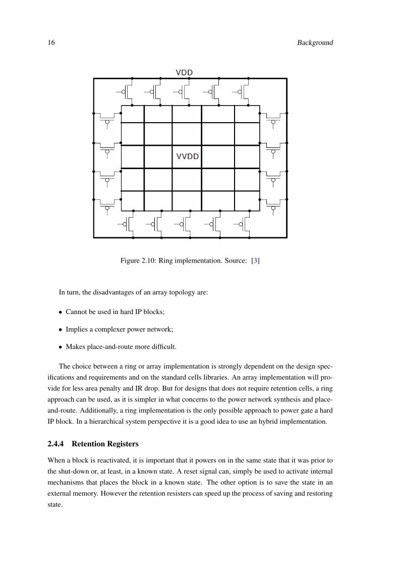
2.4.3.3 Ring vs Array
In a coarse grained implementation two topologies for the power switches placement can be used.
They can be placed around the power gated block (ring) or within it (array). The advantages and
disadvantages of each one are presented below.
Figure 2.10 illustrates a ring implementation, where the power switches are placed around the
block. The always-on power supply can, likewise, form a ring or a power mesh. Another ring can
be created for the virtual power net, which, in turn, supplies the power gated block power mesh.
The advantages of a ring implementation are:

2.4 Power Gating Challenges 15
Figure 2.9: Header (left) and Footer (right) power switches. Source: [3]
• The power distribution is simpler because the power switches are confined to a specific area
and not mixed with the block logic;
• There is always a separation between the always-on power supply and the switched/virtual
power supply. For this reason, it provides two distinct power islands, one for each power
supply, making place-and-route simpler;
• It is the only possible approach when power gating an already existing hard IP that doesn’t
allow physical changes.
The disadvantages of a ring implementation are:
• Always-on cells like retention registers cannot be used;
• Implies bigger area overhead;
• Requires a larger number of power switches, since they are farther away to the block, thus
having to drive bigger power nets. For the same reason the IR drop impact is significantly
bigger and can be difficult to manage.
In an array topology the power switches are placed across the power gated block logic. They
form a grid that connects the always-on power supply to the virtual power supply, as illustrated in
Figure 2.11.
The disadvantages of the ring implementation are the advantages of the array topology and
vice-versa.
The advantages of an array topology are:
• The power gated block has access to both permanent and virtual power supplies, allowing
the use of always-on cells such as retention registers;
• The power switches don’t have to drive long power nets because they are closer to the block
logic. This allows for smaller IR drop and less power switches;
• It has smaller area impact, since empty spaces among the logic can be used for power
switches placement.
16 Background
Figure 2.10: Ring implementation. Source: [3]
In turn, the disadvantages of an array topology are:
• Cannot be used in hard IP blocks;
• Implies a complexer power network;
• Makes place-and-route more difficult.
The choice between a ring or array implementation is strongly dependent on the design spec-
ifications and requirements and on the standard cells libraries. An array implementation will pro-
vide for less area penalty and IR drop. But for designs that does not require retention cells, a ring
approach can be used, as it is simpler in what concerns to the power network synthesis and place-
and-route. Additionally, a ring implementation is the only possible approach to power gate a hard
IP block. In a hierarchical system perspective it is a good idea to use an hybrid implementation.
2.4.4 Retention Registers
When a block is reactivated, it is important that it powers on in the same state that it was prior to
the shut-down or, at least, in a known state. A reset signal can, simply be used to activate internal
mechanisms that places the block in a known state. The other option is to save the state in an
external memory. However the retention resisters can speed up the process of saving and restoring
state.

2.4 Power Gating Challenges 17
Figure 2.11: Array implementation. Source: [3]
A retention register, actually, contains two registers. One is the main register that serves the
normal operation of the block. The other one is an auxiliary register, less leaky, that is used to save
the main register state during a shut-down operation. Then, during power on, the auxiliary register
content is loaded into the main register.
As illustrated in Figure 2.12, the auxiliary register RET is powered by the always on supply
V DD. The main register Master/SlaveLatches which generates the output Q gets its power from
the virtual supply V DDSW .
These registers, at RTL level, can be treated as normal registers, which facilitates its inte-
gration. However they can have a big impact on area and require a special attention in order to
generate the proper SAV E and RESTORE signal.
2.4.5 Isolation Cells
As mentioned in Section 2.3, the power gated block outputs can remain floating and disturb the
operation of always-on blocks. In this context it may be necessary the introduction of isolation
cells. These cells, when active, clamp the output signals to 0 1 or to the last known state. In what
concerns to the implementation an AND gate can be used to clamp a signal to 0, while an OR
gate is able to clamp to 1. The decision of which value to clamp an output signal depends on
the nature of the design. The best way is to clamp the signals to a neutral value in order not to
induce inappropriate behaviours in the always-on blocks. Most of the times this means clamping
to 0. Another reason for clamping outputs to 0 is that when two consecutive power gated and

18 Background
Figure 2.12: Retention register. Source: [3]
deactivated blocks exist, if the sink block is implemented with header switches and the outputs
are clamped to 1, a leaky path is established between the outputs and ground. This way, signals
should be clamped to 0 [3].

Chapter 3
Interface and Project Requirements
This chapter presents the existing Synopsys interface and the project requirements as established
by Synopsys design team. Due to confidentiality matters, the details given about the interface
will be limited to the strictly necessary for understanding this power gating implementation. First,
some information about the interface functionality is shown as well as data concerning area, gate
count and power consumption. Then, the problem is enunciated, also giving the reader the planned
course of action taken to fulfil the objectives.
3.1 SNPS high-speed interface
The high-speed interface that is the object of this dissertation is the digital RX (receiver) of an RX
lane, which can be called PHYGNRX. Each lane is composed by the stated digital block, hence
called rxlanedig and an AFE (analogue front end) denominated PHYGNRXAFE. Data bursts are
received through the AFE by a differential line.
It is a state of the art Synopsys interface widely used in mobile applications and is still a young
interface in its first stages of development, having much space for expansion. Its functionality
makes it a perfect power gating target. It has short periods of activity, followed by long periods of
inactivity.
In what concerns to the functionality, this interface presents two main operating modes: HS-
mode (high-speed) and LS-mode(low-speed), each one with different scenarios that are not rel-
evant for this implementation. These modes represent the bursty activity, thus the dissipation of
dynamic power. Additionally, the interface features a low power mode called Hibernate. While
in this operating mode the interface operation is halted and the line is at DIF-Z (both lines have
the same voltage). In this state all the clocks are gated through the low power technique Clock
Gating [8], thus the only source of power dissipation is leakage currents. Table 3.1 presents the
maximum clock frequency of each mode.
The interface between the rxlanedig and PHYGNRXAFE contains a set of signals that con-
trols the entry and exit of the low power Hibernate state. The change from HS-mode/LS-mode
to Hibernate is achieved through the control of an internal configuration register which can be
19

20 Interface and Project Requirements
Table 3.1: Maximum clock frequency of each operating mode
Operating Mode Max. FrequencyLS-mode 9 MHzHS-mode 600 MHzHibernate Clock Gated
accessed though a design input port. The opposite operation is controlled by a block located in
the AFE. This block monitors the state of the line and detects a transition from DIF-Z to DIF-N,
which means the end of the Hibernate state. This block, hence called SQUELCH has the following
signals interfacing with rxlanedig:
• rx_sq_en: SQUELCH input that enables the block operation;
• rx_sq_on: SQUELCH input that activates the block operation when entering Hibernate;
• rx_sq_out: SQUELCH output that signals when a transition from DIF-Z to DIF-N is de-
tected, triggering the Hibernate state exit.
Figure 3.1 illustrates the PHYGNRX architecture considering the DIGITAL/ANALOGUE
interface signals.
Regarding the power supplies, rxlanedig block is powered by the PHYGNRXAFE. Table 3.2
presents a summary of the existing power supplies. Figure 3.2 illustrates the supplies connections.
Table 3.2: Supply Voltages
SupplyVoltage
MIN TYP MAXAnalogue power VPH 1.8 1.8 1.98Common ground GD 0 0 0Top level digital power VP 0.81 0.9 0.99rxlanedig power VDD (connected to VP) 0.81 0.9 0.99rxlanedig ground VSS (connected to GD) 0 0 0
3.1.1 Physical and Power Consumption data
This section presents interesting data about rxlanedig, the target of this implementation. After
the power gating implementation these information will be compared to the final design data to
evaluate the losses and gains. Table 3.3 presents area related information.
In what concerns to corner dependent analyses, through this dissertation the following corners
will be considered (for an explanation of the corner concept see Sections 4.2.1 and 6.7.1):
• Fast Corner (FC) - fast process, 0.99V supply voltage, 125 C;
• Slow Corner (SC) - slow process, 0.81 V supply voltage, -40 C;

3.2 Project Requirements 21
Figure 3.1: PHYGNRX blocks diagram
• Typical Corner (TYPC) - typical corner, 0.9 V supply voltage, 25 C.
FC and SC are the extreme corners in what concerns to timing, being the SC the slower. In a
IR drop point of view, the FC is the one for which this metric is worst. TYPC represents the most
likely operating conditions.
Finnaly, Tables 3.4, 3.6, 3.5 presents the rxlanedig power consumption for, respectively, FC,
TYPC and SC.
3.2 Project Requirements
As mentioned in Section 1.2 the main goal of this dissertation is the power reduction of the high-
speed interface rxlanedig. Giving the description of the interface, the reader is now in position to
understand the detailed project requirements as established by Synopsys design team:
1. Isolate the whole digital block rxlanedig in a power island;
2. Insert power switches in a way that enables shutting power off to rxlanedig when this is in
Hibernate mode;
3. The power switches enable signal should be a design input port in order to give this control
to the SoC where this IP could be integrated;
4. When in Hibernate mode the SQUELCH control should also be given to the SoC;
5. Adapt the standard design flow to allow the power gating implementation;
6. Complete the entire design flow.

22 Interface and Project Requirements
Figure 3.2: PHYGNRX supply connections
Table 3.3: Physical data
Characteristic ValueNumber of cells 21019Total cell area 22297.032258 µm2
Gate count ( total_cell_areaarea_nand1 ) 43464
Total floorplan area (including the AFE) 114300 µm2
Table 3.4: Power consumption fot the FC
Operating Mode Dinamic Power Leakage Power (Static) Total PowerHS-mode 5.64 mW 5.88 mW 11.52 mWLS-mode 188.9 µW 5.8 mW 5.9889 mWHibernate 0 µW 5.77 mW 5.77 mW
Table 3.5: Power consumption fot the TYPC
Operating Mode Dynamic Power Leakage Power (static) Total PowerHS-mode 4.33 mW 32.0 µW 4.362 mWLS-mode 144.7 µW 31.6 µW 176.3 µWHibernate 0 µW 31.4 µW 31.4 µW
Table 3.6: Power consumption for the SC
Operating Mode Dynamic Power Leakage Power (Static) Total PowerHS-mode 3.27 mW 1.25 µW 3.27125 mWLS-mode 112.6 µW 1.25 µW 113.85 µWHibernate 0 µW 1.25 µW 1.25 µW

Chapter 4
Standard design flow
Having defined which goals to pursue, the first stage of this project is to study and understand the
standard design flow as used in Synopsys. Understanding it will allow to know what needs to be
changed and what is kept in order to implement power gating. The design flow can be divided into
two parts: Frontend design flow and Backend design flow. Both together, allow the creation of a
functional chip from scratch to production. The frontend flow will be briefly described, while the
backend flow is deeply analysed. It is also a concern of this chapter to associate each design flow
stage to the specific Synopsys tool used to perform it.
4.1 Front End Flow
The frontend flow is responsible to determine a solution for a given problem or opportunity and
transform it into a RTL circuit descpription. The stages of the frontend flow are identified in Figure
4.1 and described below.
1. Problem and Solution Specification
Every project starts with a problem to be solved, an opportunity to take advantage of or
something that needs to be improved. The designer needs to architect an abstract solution to
that problem that may or not, at this stage, be tied to any specific implementation technology.
One can say: "I’m going to design a circuit that receives a frame of pixels representing the
position of a target and it will track the position through the linear least squares method".
2. High-level architecture
The next step is to architect a system, diving it in high level blocks each one with a specific
functionality and determine the way they communicate. In the case of a microprocessor this
means splitting the design in the ALU, instructions decoder, registers, etc.
3. Low-level functional specification
23

24 Standard design flow
Figure 4.1: Frontend design flow.
At this stage, the designer needs to describe each block functionality and how it is imple-
mented. It may be helpful to describe the blocks using functional/behavioural descriptions
using Matlab scripts.
4. RTL Coding
Each block is described using an Hardware Description Language, like verilog. Each block
functionality is "converted" into synthesizable constructs specific to the language.
5. Integration and Functional verification
This is the stage where the functional characteristics of the design are simulated or verified,
at every level of abstraction. In order to test if the RTL code meets the functionality require-
ments, every block should be verified. Then, when every block meets its specifications, it
is time to integrate them in a top-level and verify the whole system functionality. For that
testbenches are used. A test bench generates the input test vectors to stimulate the block or
top-level functionality. Then the DUT (device under test) outputted wave forms are anal-
ysed. In complex designs the testbecnch itself checks the outputs by comparing them with
expected values.

4.2 Backend flow 25
4.2 Backend flow
The backend process is responsible for the physical implementation of a circuit. It transforms
the RTL circuit description into a GDSII layout file. The main phases of the backend process are
Synthesis and Place&Route. Figure 4.2 illustrates the backend flow and related Synopsys tools.
Figure 4.2: Backend design flow and related Synopsys tools.

26 Standard design flow
4.2.1 Synthesis
Synthesis is responsible for converting the RTL description into a structural gate level based netlist.
This netlist instantiates every element (standard cells and macros) that compose the circuit and its
connections in a way that allows meeting the design constraints regarding timing or area. Synthesis
can be described as follows: Synthesis = Translation + Optimization + Mapping.
Synopsys Design Compiler (DC) is the tool used to perform a logical synthesis. Its inputs are:
• The RTL description – Verilog or VHDL;
• The GTECH library – General technology library. Not tied to any specific technology (gates,
flip flops);
• DesignWare Library –Synthetic library (adders, multipliers, comparators, etc).
• The standard cell library – the specific target library;
• The defined constraints – synthesis goals regarding timing, area, capacitance, max transi-
tion, fanout.
• Design Environment: The operating conditions (libraries corners), wire load models.
The targeted standard cells belong to a library that is provided by a foundry. Each logic
function is implemented in several gates to accommodate several drive strength capabilities and
different fan-outs. The gate library is characterized in a way the, for each gate, defines its function,
shape, area, pins, timing and power characteristics. A target library is characterized for different
operating conditions, the so called corners. Each corner represents a PVT (process, voltage, tem-
perature) condition. For instance a standard cell library can be characterized for a technology
process of 28nm, supply voltage of 0.99V and temperature of 125 C. A cell belonging to a library
characterized for this corner have different characteristics that the logic equivalent cell of a library
characterized for a different one.
In what regards the synthesis itself as done by DC, the tool first reads the RTL description
to its memory and translates it into an unmapped GTECH netlist. Then, considering the design
constraints and design environment, DC compiles the GTECH netlist into the target library cells
and optimizations are made to meet the design constraints. For this phase, all clock, sets and
resets signals are marked as ideal, since synthesis is a process with limitations regarding physical
characteristics. Finally a set of reports are written and a gate level netlist is exported to be used by
the place and route tool. Figure 4.3 shows the functional flow of synthesis using Synopsys Design
Compiler.
4.2.2 Synthesis Verification
The first step is to verify a set of reports, which have information about timing, area, fanout and
shows the violations to the defined constraints. These reports must be interpreted to check if there
4.2 Backend flow 27
Figure 4.3: Synthesis as done by DC.
are violations (setup time, hold times, area, max transition, etc.). In case of violations DC can
try to fix them by running optimization algorithms. If DC cannot fix the violations, one must go
back to RTL coding. With these reports it is possible to check if the design is synthesizable and,
therefore, if it is possible to proceed. The final verification before proceeding to Place&Route is
to run Formality, which is a logical verification tool. It takes the final netlist generated by DC and
checks the logical equivalence with the RTL description.
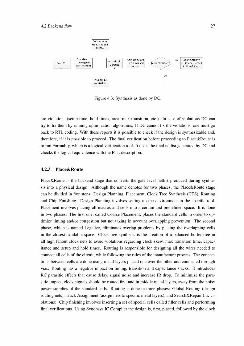
4.2.3 Place&Route
Place&Route is the backend stage that converts the gate level netlist produced during synthe-
sis into a physical design. Although the name denotes for two phases, the Place&Route stage
can be divided in five steps: Design Planning, Placement, Clock Tree Synthesis (CTS), Routing
and Chip Finishing. Design Planning involves setting up the environment in the specific tool.
Placement involves placing all macros and cells into a certain and predefined space. It is done
in two phases. The first one, called Coarse Placement, places the standard cells in order to op-
timize timing and/or congestion but not taking in account overlapping prevention. The second
phase, which is named Legalize, eliminates overlap problems by placing the overlapping cells
in the closest available space. Clock tree synthesis is the creation of a balanced buffer tree in
all high fanout clock nets to avoid violations regarding clock skew, max transition time, capac-
itance and setup and hold times. Routing is responsible for designing all the wires needed to
connect all cells of the circuit, while following the rules of the manufacture process. The connec-
tions between cells are done using metal layers placed one over the other and connected through
vias. Routing has a negative impact on timing, transition and capacitance slacks. It introduces
RC parasitic effects that cause delay, signal noise and increase IR drop. To minimize the para-
sitic impact, clock signals should be routed first and in middle metal layers, away from the noisy
power supplies of the standard cells. Routing is done in three phases: Global Routing (design
routing nets), Track Assignment (assign nets to specific metal layers), and Search&Repair (fix vi-
olations). Chip finishing involves inserting a set of special cells called filler cells and performing
final verifications. Using Synopsys IC Compiler the design is, first, placed, followed by the clock

28 Standard design flow
tree synthesis (CTS) and, finally the routing of every cell and chip finishing. The result is a post-
layout netlist and a GDS II file. The steps taken to perform Place&Route using ICC are as follows:
Design planning
1. Create one empty Milkyway library.
The Milkyway library is the design database. It used for portability throughout all Synopsys
design environment. This library is linked to the standard cells library and to the technology
file. This file defines the physical rules and characteristics like the resistivity of each metal
layer (a deeper explanation of libraries and technology file is given in Sections 6.7.1 and
6.8).
create_mw_lib $design_lib -technology $tech_file
2. Load Synthesis netlist.
It is the netlist created by Design Compiler. It will be linked to the previously loaded phys-
ical and standard cells library.
read_verilog $verilog_file
3. Connect the standard cells power pins to the design power supplies.
derive_pg_connection $pwr_net $gnd_net $pwr_pin $gnd_pin
4. Load TLU+ files
TLU+ files are provided by the foundry and give important information about the parasitic
effects between cells and nets. This information will be used to correctly place and route all
cells.
load_tlup
5. Load the floorplan
The floorplan is the initial physical shape of the circuit. It has information about the cir-
cuit boundaries, the I/O pin location, the places where standard cells cannot be placed and
the upper metal power straps. These straps are done in upper metal in order to have less
resistance and smaller IR drop. The floorplan is previously done using Synopsys Custom
Designer that produces the TCL scripts to be loaded by ICC.
source boundary.tcl
source floorplan.tcl
source pins.tcl

4.2 Backend flow 29
6. Load the design constraints
Placement and routing are done in order not to violate these constraints. A TCL file is given
with tool specific commands that define the design constraints.
source design_constraints.tcl
7. Check for special design constraints.
Some standard cells libraries demand the use of special cells:
• Tap cells – Polarization cell that are added by rows;
• End cap cells and filler – Placed for nwell continuity. Added in several ways like the
beginning or end of each row or between standard cells.
Placement
8. Perform the coarse placement.
Place the cells inside the floorplan. They will be placed in order to meet timing but not
avoiding overlapping cells.
create_placement
9. Legalize the placement.
Legalize is the process of eliminating overlap problems by placing overlap cells in the clos-
est available space.
legalize_placement
10. Physically connect the placed cells to power and ground.
Connections are done by creating lower metal supply rails and connect them to the existing
upper metal straps using vias.
preroute_standard_cells
Clock Tree Synthesis
11. Compile clock tree
compile_clock_tree
12. Check the clock tree for errors.
Check if any cell has big transition times, capacitance, or high fanout. Weak cells with
high fanout produce huge transition times. In order to balance the clock tree it is possible
to replace the weak cell by a stronger and logical equivalent one. On the other hand cells
driving long nets can produce high transition times as well. One solution can be placing a
strong buffer in the output of the driver cell.

30 Standard design flow
13. Perform a IR drop analysis.
At this stage, before routing, it is important to check the IR drop over the circuit. ICC will
output a color map representing the IR drop from the power straps and across all the circuit.
The red spots on this map show high IR drops. It is also possible to have an idea of the
circuit power consumption.
dump_ir_drop
14. Run a Static Timing analysis from ICC.
Running a STA from ICC at this stage allows detecting timing violations at this stage of the
design. ICC can try to eliminate these violations automatically by accelerating or delaying
paths.
Automatic Optimization: psynopt
Routing
15. Route the clock nets.
Route the high sensitive clock nets first. route_zrt_group -all_clock_nets
16. Route signal nets.
At this stage ICC will try to preserve the previously routed clock nets.
route_zrt_auto -max_detail_route_iterations 20
Chip Finishing
17. Check for errors.
Check for DRC and timing errors. If big violations exist, ICC can try to fix them automati-
cally.
route_opt -effort high -incremental
Setup time violations can be fixed by accelerating the path, which can be done by replacing
cells by stronger and logical equivalent ones. To fix hold time violations the path has to be
delayed. This is achieved by inserting buffers into the logical path.
18. Place FILL and DCAP cells in the empty gaps.
Place FILL DCAP cells to establish nwell continuity.
insert_stdcell_filler -cell_with_metal $decap_cells
insert_stdcell_filler -cell_without_metal $filler_cells
19. Run DRC and LVS.
To check if the Place&Route process respected all rules.

4.2 Backend flow 31
verify_drc
verify_lvs
20. Save the Milkyway database and the post-layout netlist.
21. Proceed to sign off
At this stage the post layout netlist is ready to be verified by the sign of timing, power, DRC
and LVS tools.
4.2.4 Parasitic extraction
Parasitic extraction has the objective to create an accurate RC model of the circuit so that future
simulations and timing, power and IR Drop analyses can emulate the real circuit response. Only
with this information, all the analyses and simulations can report results close to the real func-
tioning of the circuit. This way this stage needs to precede all signoff analyses. Star RCXT is
the Synopsys tool capable of performing parasitic extraction. It takes the post-layout Milkyway
database and the NXTGRD files provided by the foundry (cells parasitic information) and pro-
duces SPEF (Standard Parasitic Exchange Format) and SBPF (Synopsys Binary Parasitic Format)
files.
4.2.5 Static Timing Analysis (STA)
STA is a method to obtain accurate timing information without the need to simulate the circuit.
It allows detecting setup and hold timing violations, as well as skew and slow paths that limit
the operation frequency. Synopsys PrimeTime allows running STA over a physical design, for
each corner. Taking as inputs the post-layout netlist and parasitic and standard cells information
it outputs a series of reports, which give the possibility to detect timing violations. As mentioned
before these timing violations can be fixed by inserting buffers or resizing cells. With PrimeTime
it is possible to identify where to perform these modifications and test them. When a list of new
buffers and resized cells is available, the modifications need to be done back in ICC, followed by
another parasitic extraction and STA to check the results. This process is done iteratively until no
violations are reported.
4.2.6 Post-layout Analysis and Verification
Once again, formality should be run to check the logical equivalence of the post-layout netlist
with the RTL description. The huge number of transistors in a circuit can make the voltage level
drop below a defined margin that ensures that the circuit works properly. IR Drop analysis allows
checking the power grid to ensure that it is strong enough to hold that minimum voltage level.
Synopsys PrimeRail is the tool that outputs IR-drop and EM analyses reports. Then, PrimeTime-
PX, which is an extension of Prime Time, is the tool responsible of performing power analyses to
estimate the power consumption of the circuit, for each corner. It has the capability of computing

32 Standard design flow
the dynamic and static power consumption of the whole design or the power consumption of each
cell or macro.
4.2.7 Integration and DRC/LVS Verification
The final step is to generate a GDSII file of the entire design layout. For that Custom Designer can
be used to integrate the GDSII layout of the standard cells and the one outputted by IC Compiler,
thus creating the final and complete graphics layout file. Finnaly, the Synopsys DRC/LVS verifi-
cation tool, Hercules, is run. DRC (Design Rules Checking) checks if the foundry geometric and
connectivity rules are met. Examples of DRC’s include: Metal to metal spacing; well to well spac-
ing; minimum metal width; Antenna Effect; Metal fill density. LVS (Layout Versus Schematic)
checks if the physical circuit corresponds to the original circuit schematic. The schmatic is a CDL
netlist and the layout is the GDSII stream.
4.3 Summary
Throughout this chapter the standard design flow using Synopsys tools was depicted. Keeping in
mind the power gating implementation, it is possible to understand that there is no focus on power
characteristics. With this flow, every design is assumed as being a single-supply design. It is, then,
necessary to understand how to use these tools taking into account power intent and how to intro-
duce power gating related cells. It is important to mention that a power gating implementation has
its focus on the physical implementation, thus, the steps Place&Route and Post-layout Analysis
and Verification are where this dissertation will have its main impact.

Chapter 5
Low Power Design Flow
This chapter documents the main changes that need to be made to the original high-level design
flow presented in the previous chapter. The main objective is to understand how to inform the tools
about the existence of different power domains and power islands and ho to insert power gating
related cells like power switches, retention registers and isolation cells. Each tool specific flow
and modifications are shown in Chapter 6.
5.1 Power Intent Specification using UPF
The answer to the first problem is to use the IEEE 1801 Standard for Design and Verification of
Low Power Integrated Circuits, also known as the Unified Power Format (UPF) [11]. It consists
in a set of Tcl-like commands that allow to specify the power intent for electronic systems. Using
UPF the designer is able to specify the different power domains of a system, the supply network,
power switches, isolation and retention strategies, power states and other aspects related with the
power management of a chip design. This is even more convenient due to the the fact the Synopsys
tools supports the UPF standard across all design flow.
5.1.1 UPF Concepts
Although the UPF standard allows to specify the power characteristics of a chip design it doesn’t
specify how those requirements are implemented, in other words, it is just an abstract description
of a design strategy that is interpreted and implemented by Synopsys tools.
The first and more important construct of an UPF specification is the power domain. It is
an abstract group of elements that share the same power characteristics in a design. Typically all
these elements are connected to the same power supply and ground, the so called primary power
and primary ground. It is also possible to define other power supplies for a domain as it will be
shown is Section 6.3. A power domain is physically translated into a voltage area. Each power
domain is defined within a context and has a set of design elements belonging to it. The scope is
the hierarchy level at which the domain is defined.
33

34 Low Power Design Flow
Each power domain has supply nets and supply ports associated with it. A supply net carries
a supply voltage or ground across a power domain. A supply net that is associated with more
than one power domain is said to be "reused". A supply port is the connection point between two
adjacent levels of hierarchy.
A supply set is a collection of supply nets. Each net serves a particular function (power,
ground, pwell and nwell polarizations)regarding to a power domain. A supply set can be used for
each domain or standalone supply nets can be created and then associated to a power domain. The
first option is useful when power domains have a large set of supply nets associated. Otherwise,
not using supply sets can be simpler and sufficient.
The power switch as defined in Section 2.3 is also an UPF element. A power switch has
an input supply net (always-on), an output supply net (switched), and at least one input signal to
control the switching activity. Optionally an acknowledge signal can be defined representing the
moment when a power switch has finished its power on sequence.
A Power State Table lists the possible combinations of voltage values (power states) for all
domains in the design.
Besides the elements described above, which are the mandatory constructs for a power gating
implementation, UPF standard also defines isolation cells and retention registers. These cells, as
explained in Chapter 2 can be used to, respectively, isolate power-gated blocks IO ports and to
retain data during shutdown.
The UPF syntax to be used when implementing power gating will be described in Chapter 6.
5.2 Low Power Flow Using Synopsys Tools
As mentioned in the previous section the UPF standard allows to describe the whole power intent
of a chip design. This characteristic makes possible the use of a golden RTL description without
any modifications (since it does not contain power pins instantiation) and complement it with an
UPF file. Then, Synopsys tools are prepared to read the UPF file and use it along the entire flow,
updating it when necessary. Figure 5.1 illustrates the design flow using the UPF standard and
Synopsys tools [2].
Begining from the Synthesis step, Design Compiler reads the golden RTL logic description
and the golden UPF power intent specification in order to synthesize a gate-level netlist. This
netlist, besides, the logic normal gates, contains special cells like retention registers and isolation
cells, added according to the UPF description [12]. Design Compiler also outputs an updated
UPF file (UPF’). This file contains the original UPF information plus the supply connections for
special cells created during synthesis.
In the physical implementation step, IC Compiler reads the gate level netlist and the UPF’
file. The UPF information is used to create the needed voltage area for each power domain and to
logically connect every supply pin to its correspondent supply net. More importantly, the power
switches are physically placed in this step, taking into account the information of the UPF’ file.
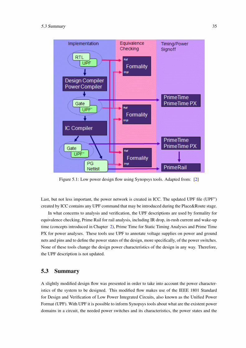
5.3 Summary 35
Figure 5.1: Low power design flow using Synopsys tools. Adapted from: [2]
Last, but not less important, the power network is created in ICC. The updated UPF file (UPF”)
created by ICC contains any UPF command that may be introduced during the Place&Route stage.
In what concerns to analysis and verification, the UPF descriptions are used by formality for
equivalence checking, Prime Rail for rail analysis, including IR drop, in-rush current and wake-up
time (concepts introduced in Chapter 2), Prime Time for Static Timing Analyses and Prime Time
PX for power analyses. These tools use UPF to annotate voltage supplies on power and ground
nets and pins and to define the power states of the design, more specifically, of the power switches.
None of these tools change the design power characteristics of the design in any way. Therefore,
the UPF description is not updated.
5.3 Summary
A slightly modified design flow was presented in order to take into account the power character-
istics of the system to be designed. This modified flow makes use of the IEEE 1801 Standard
for Design and Verification of Low Power Integrated Circuits, also known as the Unified Power
Format (UPF). With UPF it is possible to inform Synopsys tools about what are the existent power
domains in a circuit, the needed power switches and its characteristics, the power states and the

36 Low Power Design Flow
supply connections. This way the the RTL golden description can still be used alongside with the
UPF specification.

Chapter 6
Power Gating Implementation
This is the section where the steps taken in order to implement power gating are described. The
low power design flow is complemented with the specifics steps that need to be taken for each flow
stage and respective tool. The objective is to present what was made in this specific implementa-
tion and, at the same time, the needed methodology is explained.
6.1 Power Gating Strategy
Before proceeding with the design flow some decisions should be made in advance. The first one is
what switches topology to use. As explained in Section 2.4.3.3 there are two possible approaches:
Ring or Array. In this case, the objective is to power gate an entire digital hard IP that does not
allow physical modifications. Thus, the only possible solution is to use the Ring implementation
and place power switches around the IP. This will also make the power network synthesis simpler,
with only two digital power domains. The problems with this solution are bigger IR drop and
bigger area overhead that need to be carefully handled.
The second decision that needs to be made is whether to use Header Switches (PMOS) or
Footer Switches (NMOS). This decision is limited by the standard cells library. The available
library in Synopsys only features header switches, making them the only option.
Retention registers cannot be used for the same reason that an array of power switches is
impossible.
Since this design is composed of only one digital block, its floating outputs (when power
gated) wont affect an non existing always-on block. This way, isolation cells are not absolutely
necessary and their use would have a negative impact on area. However this cells should be added
at the SoC level where this IP could be integrated.
6.2 Frontend stage
As already said, this implementation has its main focus on the physical implementation and ver-
ification. Nevertheless, a little "backend work" is needed. The first problem arises from the fact
37

38 Power Gating Implementation
Figure 6.1: Blocks diagram of the modified design.
that, when the digital rxlanedig block is powered-off, the AFE still needs to receive the control
signals related with the squelch block. Considering this fact, Synopsys defined as a requirement
that the squelch control signals are given to the SoC (Section 3.2). It is useful to remember that
the control signals are rx_sq_en and rx_sq_on (see Section 3.1). This way, two extra input ports
need to be added to the design. The operating principle is easy: when the rxlanedig is powered
on, the control comes from it; when powered off, the control comes from the input ports. This be-
haviour is achieved using a simple multiplexer for each signal. Therefore, a new block containing
two multiplexers was added. Another requirement is also to give the control of the power switches
to the SoC. To fulfil these requirement another input port was added, RX_SQ_CTR_SOC. Still,
in what regards the power switches control a port was added to be used as an acknowledge of the
moment when the power switches have finished their power on sequence. The new design blocks
diagram is shown in Figure 6.1. Note that the output port RX_SQ_ACK_SOC is yet not con-
nected because it will be later connected to the power switches. These new specifications resulted
in a new block and in modifications in the top level where all blocks and IO ports are instantiated.
All the RTL files are described using Verilog.
6.3 Describing the power intent using UPF
Once the golden RTL files are ready, it is time to describe the power specifications in an UPF file.
For the definition of the UPF constructs used to specify the power intent, refer to Section 5.1.1.
The first step is to define the power domains. For this implementation we need to create three
power domains, as illustrated in Figure 6.2. In order to specify the power domains the following
UPF commands are used:
create_power_domain TOP
create_power_domain PD_DIG -elements rxlanedig
create_power_domain PD_AFE -elements PHYGNRXAFE

6.3 Describing the power intent using UPF 39
Figure 6.2: UPF diagram.
When creating the power domain called TOP, without specifying any element that it might
contain, every element of the design, that does not belong to any power domain yet, is automati-
cally associated with it. TOP contains the always on digital cells, like the multiplexers. PD_DIG
is created with the digital rxlanedig IP associated with it, while PD_AFE contains the analogue
block PHYGNRXAFE.
The next step is to specify the supply nets and connect them to supply ports. In this implemen-
tation it was chosen not to use supply sets, since each power domain as a relatively small number
of nets, mainly one power and one ground net. Thereby, each net is created and associated with one
or more power domains.In this implementation VP is the always-on net, which is associated with
the always-on domain TOP and the analogue domain PD_AFE. VPH is the analogue power net,
thus associated with PD_AFE. VPS_DIG is the switched power net, used to power rxlanedig and,
this way, associated with PD_DIG. Finally, GD is the supply net used to distribute the common
ground. The supply nets creation is achieved using the following commands:
create_supply_net VP -domain TOP
create_supply_net VP -domain PD_AFE -reuse
create_supply_net VPH -domain PD_AFE
create_supply_net -domain TOP -reuse VPH
create_supply_net VPS_DIG -domain PD_DIG

40 Power Gating Implementation
create_supply_net VPS_DIG -domain TOP -reuse
create_supply_net GD -domain TOP
create_supply_net GD -domain PD_DIG -reuse
create_supply_net GD -domain PD_AFE -reuse
The supply ports of this design are specified using the following commands:
create_supply_port VP
create_supply_port GD
create_supply_port VPH
Note that only top level ports are created once both digital and analogue blocks already have
power ports. Normally, a supply port should be created whenever a supply net crosses power
domains. The connection between the supply nets and supply ports is achieved with:
connect_supply_net VP -ports VP
connect_supply_net VPH -ports VPH
connect_supply_net GD -ports GD
Still in the supply nets context, one needs to define the main supply nets for each power
domain. The UPF standard defines that a power domain as a primary power net and a primary
ground net. All power pins of all elements of a certain power domain are connected to that nets.
PD_AFE has the particularity of having two power nets associated with it. This way, one of
the nets should be explicitly connected to its power pin. It was chosen to explicitly specify the
connection between VPH and vph port (see Figure 3.2). Note that the primary supply net of
PD_DIG is VPS_DIG, the switched power net. This way all elements contained in this domain
will be power gated. The following commands were used:
set_domain_supply_net TOP
-primary_power_net VP
-primary_ground_net GD
set_domain_supply_net PD_DIG
-primary_power_net VPS_DIG
-primary_ground_net GD
set_domain_supply_net PD_AFE
-primary_power_net VP
-primary_ground_net GD
connect_supply_net VPH -ports I01MPHYGNRXAFETYPE1/vph
A power switch designated (PD_DIG_SW) is specified to switch power to the domain PD_DIG:
6.3 Describing the power intent using UPF 41
create_power_switch PD_DIG_SW
-domain TOP
-input_supply_port VDDP VP
-output_supply_port VDDC VPS_DIG
-control_port RX_SQ_CTR_SOC RX_SQ_CTR_SOC
-ack_port RX_SQ_ACK_SOC RX_SQ_ACK_SOC
-on_state on_state VDDP !RX_SQ_CTR_SOC
Note that the specified domain is TOP. These means that this switch is to be placed in the TOP
domain, which has both input and output nets associated. However, the controlled domain is still
PD_DIG. The -input_supply_port and -output_supply_port options allow to specify
the input and output supply nets and their connections to supply the ports of a certain switch. In
this case the input switch supply port VDDP is connected to the input supply net VP. In turn,
the output switch supply port VDDC is connected to net VPS_DIG. The switch is controlled by
the port RX_SQ_CTR_SOC and is connected to the acknowledge port RX_SQ_ACK_SOC. The
-on_state option allows to specify the boolean function of the control port for which the switch
is considered to be on, meaning that the output net is powered.
Lastly, one needs to specify the power states of the chip, which means, the different voltage
values of the different power ports. The first step is to define the port states for each power port,
including the power switch output port. The following UPF commands define the port power states
for the operating conditions corresponding to the FC (fast process, 0.99V and 125 C).
add_port_state VP -state TOP_VP 0.99
add_port_state GD -state GND 0.0
add_port_state PD_DIG_SW/VDDC
-state POWER_ON 0.99
-state POWER_OFF off
add_port_state VPH -state TOP_VPH 1.98
Note that the switch power output port PD_DIG_SW/VDDC has two states. The one corre-
sponding to the moments when the switch is on and a second state for the opposite situation. The
former state has an associated voltage of 0.99 while the latter uses the keyword off. The state
names can be defined according to the user’s will. These names are, now, used to create a Power
State Table (PST). This table has an entry for each possible voltage combination of the supply nets.
Each entry associates every supply net to an already defined power state. In this implementation
the PST is defined in the following way.

42 Power Gating Implementation
create_pst PST -supplies VP VPS_DIG GD VPH
add_pst_state ON -pst PST -state TOP_VP POWER_ON GND TOP_VPH
add_pst_state OFF -pst PST -state TOP_VP POWER_OFF GND TOP_VPH
At this point the UPF file is ready to be used and it is possible to proceed to synthesis.
6.4 Synthesis using Design Compiler
Considering the UPF specification, synthesis turns the RTL description into a gate-level netlist, as
described in Sections 4.2.1 and 5.2.
In this implementation this process is done in a very straight forward way. The analogue and
digital block are already existing physical designs, thus they don’t need to be synthesized. In the
other hand, as explained in Section 6.1, this implementation doesn’t require the use of retention
registers or isolation cells. Thus, no cells are added as a result of the UPF specification. This
way, the already exiting blocks are black boxes and the only RTL code that will be translated
to gates is the one regarding the control of the SQUELCH related signals (see Chapter 3). The
resulting gate-level netlist instantiates both black boxes and four extra cells: two multiplexers and
two inverters, representing the SQUELCH control. For the rest of this document these four cells
will be addressed as multiplexer cells.
6.5 Formal Verification using Formality
Formality performs functional equivalence checking between the different netlists generated through-
out the flow. Formality recognizes the low power intent specified using UPF and the data supported
data comparison are as follows [13]:
• RTL + UPF versus gate-level netlist + Design Compiler updated UPF
• RTL +UPF versus post-layout PG netlist
• Gate-level netlist + Design Compiler updated UPF
The UPF file is read using the load_upf command. Formality recognizes the UPF informa-
tion and identifies the supply nets and the power states defined in the PST. When powered off, a
power gated block is considered as don’t care for the functional equivalence checking. By default,
Formality only considers the ON states. Thus, in order to perform a complete verification, it must
be instructed to consider all states defined in the PST. This is achieved by setting to FALSE the
verification_force_upf_supplies_on variable, after the load_upf command.
For this implementation, all verification were successfully completed without any issue.

6.6 Floorplan Modification using Custom Designer 43
Figure 6.3: Original floorplan.
6.6 Floorplan Modification using Custom Designer
Figure 6.3 is a snapshot of the Custom Designer tool interface showing the floorplan of the existing
PHYGNRX.
It is possible to see that the boundary is adjusted to rxlanedig and PHYGNRXAFE. The first
modification was to add extra space for placing the power switches, the four SQUELCH control
cells and to synthesise the Power Network. Thus, the floorplan shape was enlarged by 20 µm
around rxlanedig, as shown in Figure 6.4.
The second modification was to add the necessary IO ports according with the new design. The
IO ports related with PHYGNRXAFE were not placed in the boundary, but in the exact position of
the respective hard IP pin. Figure 6.5 shows the added pins.
When all modifications are done, Custom Designer outputs a set of Tcl scripts containing the
floorplan information, which is later read by IC Compiler.
6.7 Library Data Preparation
To perform its task IC Compiler reads in the gate-level netlist produced by Design Compiler and
libraries that contain information about the cells instantiated in the netlist. The multiplexer cells
and the power switches (to be created) are present in the standard cells library but the black boxes
libraries need to be created.
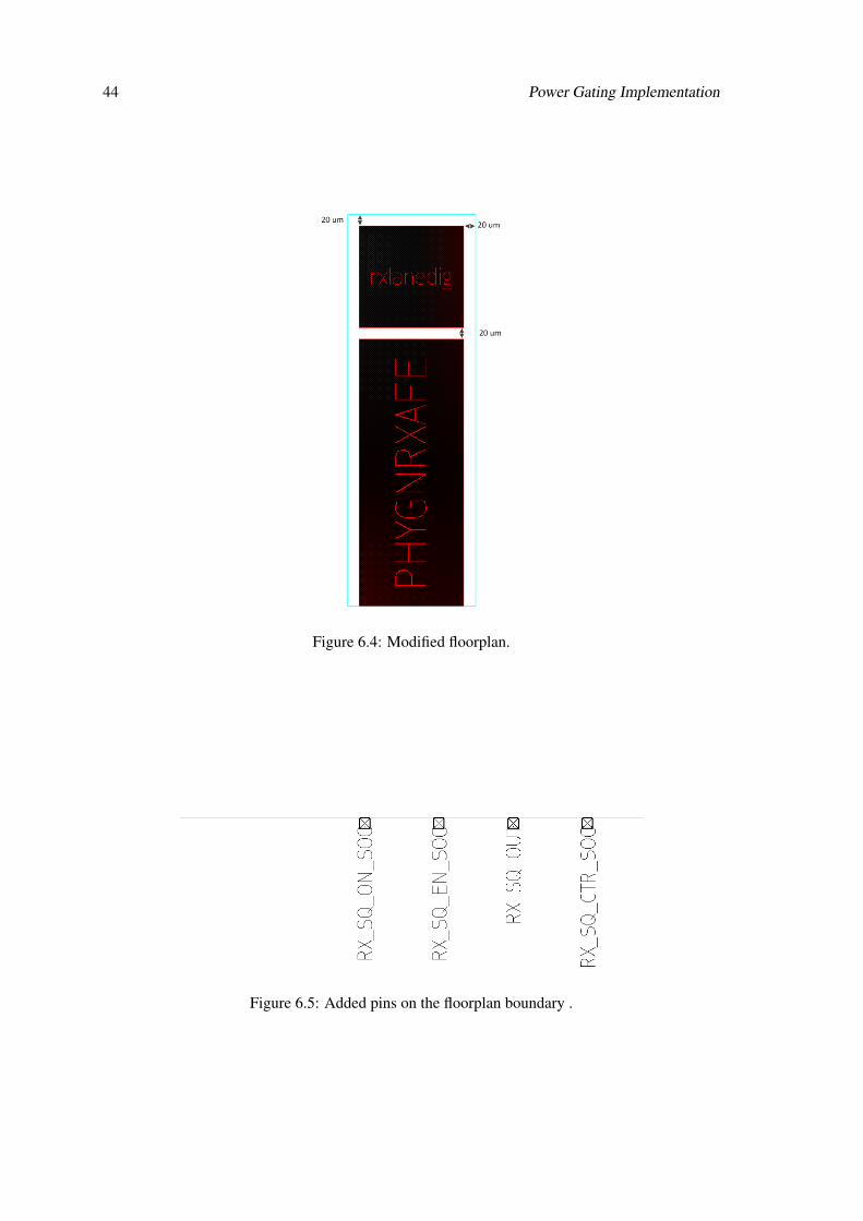
44 Power Gating Implementation
Figure 6.4: Modified floorplan.
Figure 6.5: Added pins on the floorplan boundary .

6.7 Library Data Preparation 45
6.7.1 Libraries
The physical information is contained in the Milkyway database. The design unit of a Milkyway
database is a cell. A cell can be anything from a leaf standard cell to a whole chip. Each cell is
represented by different views. The main types of views presented in a Milkyway database are:
• CELL view: The full layout of a physical cell. Contains placement, routing, pin and netlist
information;
• FRAM view: An abstract representation of a cell. It is used for placement and routing, thus,
only having information about the shape, pins, metal blockage and allowed areas for vias
connections;
• CONN view: A representation of the supply network. It is used by PrimeRail for rail
analysis.
Besides physical data, ICC also needs logical information. A logical library contains func-
tional information about the cells, like logic function, timing and power characteristics that Syn-
opsys tools use to perform optimizations and verifications. This information is contained in a set
of binary Synopsys database (.db) files. For each .db file there is an equivalent ASCII-format Ly-
berty (.lib) file. Each cell is characterized for different corners, corresponding to different PVT
(processes, voltages and temperatures) resulting in a .db and .lib file for each corner. These log-
ical libraries have to be compliant with the Liberty PG Pins Syntax. This means that each cell
characterization needs to contain supply pins related information. It will allow synthesis, physical
implementation and verification tools to properly connect the cells in the layout and to analyse
designs with different supply domains. An example of a power switch cell definition, compliant
with the Liberty PG Pin Syntax, where it is possible to see the PG pins definition is shown below.
cell ("SW4")
...
pg_pin (VDDC)
direction : output;
pg_function : "VDDP";
pg_type : "internal_power";
switch_function : "!EN";
voltage_name : "VDDC";
pg_pin (VDDP)
direction : input;
pg_type : "primary_power";
related_bias_pin : VBP;

46 Power Gating Implementation
voltage_name : "VDDP";
pg_pin (VSS)
direction : input;
pg_type : "primary_ground";
related_bias_pin : VBN;
voltage_name : "VSS";
....
6.7.2 Libraries creation
The rxlanedig Milkyway and its corresponding CELL view already existed. However a FRAM
view needs to be created for placement and routing in ICC. This FRAM view can be easily cre-
ated from the CELL, using the ICC command create_macro_fram. This command will execute a
process called blockage, pin and via (BVP) extraction.
In the case of the PHYGNRXAFE the Milkyway library has to be created from a physical data
source. This information can be provided in two ways:
• GDSII stream format, the layout data exchange format for the industry.
• LEF, data exchange format for physical libraries (Library Exchange Format).
To convert this information into a Milkyway database, the layout data needs to be read into the
Milkyway tool [14]. In addition, the information that is not provided in the LEF or GDSII file,
such as the technology file needs to be given, as illustrated in Figure 6.6.
A LEF file includes more information than just the physical layout of a GDSII file. It contains
information about the layers, vias, placement site type, macro definitions and pin types. This way,
in this implementation a LEF file was used. At this point, it is important to know that, later, in
the ICC flow, when assigning a macro cell to a power domain this cell has to have the "Hard
macro" attribute. In order to create a FRAM view with that attribute, it is mandatory that the LEF
file explicitly indicates that the corresponding cell is an hard macro using the keywords SOURCE
USER and CLASS BLOCK. Otherwise, power domains and voltage areas will not be created.
6.8 Technology File and Metal Layers
In the previous and 4.2.3 sections it was mentioned that a Milkyway library needs to be created
with an associated technology file. But what exactly is a technology file and what does it defines?
The technology file is an ASCII-format text file that informs Synopsys tools about the physical

6.9 Adding supply (PG) pins around rxlanedig 47
Figure 6.6: Library Preparation flow
characteristics of the technology process to be used. It defines which metal layers are available
and each layer physical and electrical rules.
Each metal layer has an associated direction for power and signal routing, which is presented
in Table 6.1. This directions aren’t mandatory but, when routing IC Compiler will use them,
avoiding shorts.
Table 6.1: Metal layers routing directions
Metal layer DirectionMetal 1 VerticalMetal 2 HorizontalMetal 3 VerticalMetal 4 HorizontalMetal 5 VerticalMetal 6 HorizontalMetal 7 VerticalMetal 8 Horizontal
6.9 Adding supply (PG) pins around rxlanedig
As shown by Figure 6.3, in the initial floorplan rxlanedig was placed on top of the PHYGNRXAFE,
thus only having PG pins at its bottom. In this implementation it will be powered by a ring of power
switches. The more efficient way to distribute power and ground is having PG pins placed around
the entire rxlanedig block, allowing it to receive the supplies from all sides of the ring.
This way, using IC Compiler pins in layers 6 and 8 were placed on both sides to allow hori-
zontal connections, while, pins in layers 7 were added at the top for vertical connections. One pin
was added at the beginning and end of each existing power strap. Thereby, 120 new PG pins were

48 Power Gating Implementation
Figure 6.7: Added PG pins
added. Figure 6.7 shows the upper left corner of the new rxlanedig cell with some of the newly
created pins.
6.10 Place&Route using IC Compiler
Having prepared all design libraries, the physical implementation itself can be performed. Consid-
ering the strategy presented in Section 6.1 and the UPF power intent specification, IC Compiler
will transform the gate level netlist into a physical design. Furthermore, in this design design stage
the power switches will be inserted and the power network synthesized.
According with ICC user guide [15] and some outcomes from the implementation itself,
Figure 6.8 illustrates this tool specific flow for a power gating implementation, which is described
below.
1. Read the design
The first step is to prepare the IC Compiler environment by reading all the logic and physical
libraries and setting some useful variables. For instance the UPF and technology files ab-
solute paths can be loaded into variables with the set Tcl command and be referenced
latter in the flow. Furthermore, by default, ICC creates an implicit supply set when a
power domain is created (see Section 5.1.1). To disable this feature the ICC variable
upf_create_implicit_supply_sets needs to be set to false. Then the Milky-
way library for this implementation is created and associated to the technology file and to

6.10 Place&Route using IC Compiler 49
Figure 6.8: ICC Flow for a Power Gating Implementation. Main stages highlighted in purple
the rxlanedig and PHYGNRXAFE physical libraries using the create_mw_lib command.
The last step is to read in the gate-level netlist.
2. Load Floorplan
The Tcl scripts outputted by Custom Designer are read by ICC, creating the design floorplan.
At this stage the coordinates for the macro cells are already defined and also read, which,
places them in the correct position.
3. Load UPF
The load_upf command executes the UPF commands in the specified file loading the
power intent into ICC.
4. Set net voltages
In order to completely specify the operating conditions the set_voltage command is
used to specify the operating voltage of every top-level supply nets. At this stage the
check_mv_design should be used to check the correctness of the power characteristics
specification.
50 Power Gating Implementation
5. Logically connect power and ground
In this step every power and ground pin is connected to the respective supply net. This
connection is achieved in an automatic way, without the need to explicitly specify which
power pins should be connected to which supply net. The derive_pg_connection
-create_nets -create_ports interprets the UPF specification and connects the sup-
ply pins of every cell to its power domain primary-power or primary-ground net. The
-create_nets and -create_ports command creates any non-existent power net and
port. Remember that the supply nets are not specified in the gate-level netlist, so before
using this command they do not exist, being only present in the UPF specification. The
-reconnect option updates the supply connections, connecting all unconnected supply
pins. This command issues a report about the created connections:
Power/Ground Connection Summary:
P/G net name P/G pin count (previous/current)
--------------------------------------------------------
Power net "VP": 0/6820
Power net "VPH": 1/1
Power net "VPS_DIG": 0/519
Unconnected power pins: 7339/0
Unconnected back-bias power pins: 5332/5332
Ground net "GD": 0/6821
Unconnected ground pins: 6821/0
Unconnected back-bias ground pins:
5332/5332
--------------------------------------------------------
Information: connections of 14160 power/ground pin(s) are
created or changed.
Note that the derive_pg_connection does not connect back-bias pins. These connec-
tions have to be, latter, explicitly made.
6. Create voltage areas
This very important step has the objective of creating a voltage area for each power domain.
This will turn the abstract construct of a power domain into a physical region in the layout.
For this implementation 3 voltage areas are considered, once 3 power domains were created:
PD_DIG, PD_AFE and PD_TOP. The first two voltage areas were created in the following
way:

6.10 Place&Route using IC Compiler 51
create_voltage_area -power_domain PD_DIG
-coordinates 17.710 475.260 202.315 655.745
create_voltage_area -power_domain PD_AFE
-coordinates 20.080 1.290 200.125 459.375
The -power_domain option specifies for which power domain the voltage area is being
created. This way, all elements belonging to the power domain are also associated with the
voltage area. The -coordinates allows to specify a bonding box for the voltage area.
7. Place Power Switches
In this stage, the power switch strategy specified in the UPF will be mapped into a ring
of several power switching cells, which will be placed around the specified voltage area.
The first step is to map the UPF switch into a power switching cell from the standard cells
library. Usually a library comes with a few switches with different characteristics. It is up
to the designer to choose one. The metrics for this choice are:
• The cell logic characteristics;
• The cell ON state resistance and the induced IR drop;
• The cell leakage;
• The area overhead.
The designer should choose a power switching cell that fulfils the design needs. The library
available for this implementation features eight different power switching cells. Beginning
from the functional characteristics a cell with an enable/control signal buffer is needed (see
the next stage for the justification). From the initial eight cells available in the library, only
four fulfils this requirement. Their characteristics, considering the FC (fast, 0.99V , 125 C)
are resumed in Table 6.2.
From Table 6.2, the leakage current of all cells is similar. Cells SW1 and SW3 have,
slightly, less resistance, which could lead to less IR drop. However SW1 and SW3 are
bigger. These cells are what is considered a double-height cell. It means that they occupy
two rows, instead of one occupied by SW2 and SW4. Thus, using SW2 or SW4 allows
Table 6.2: Power switching cells characteristics
Cell ON Resistance (Ω) Leakage Current (nA) Height (µm) Width (µm )SW1 218.957 -58.07 1.9 1.485SW2 332.293 -63.17 0.95 2.295SW3 236.133 -58.35 1.9 1.89SW4 298.428 -60.25 0.95 3.105

52 Power Gating Implementation
to place more switches in the same physical area, thus less IR drop. Comparing SW2 and
SW4, it is possible to verify that SW4 has less resistance, making it the switch to be used in
this implementation.
In order to map the UPF switch into the SW4 cell, the command map_power_switch is
used in the following way:
map_power_switch PD_DIG_SW -domain TOP -lib_cells SW4
The next question regarding the power switches placement is: how many to insert? It is
known that more switches means less IR drop but higher leakage and area. For an array
approach, the ICC explore_power_switch command presents a set of possible combi-
nations showing their impact. However, these feature does not work for a ring, so another
approach is needed. Giving a target IR drop for the power switching ring, Equation 6.1
gives us a way to estimate the number of switches [16].
Numberswitches =RON × Idomain
Droptarget(6.1)
where,
• RON is the switches linear resistance, when they are in ON mode,
• Idomain is the power gated domain current and
• Droptarget is the limit IR drop for the switches.
For the FC, which is the worst case scenario for IR drop, considering a target drop (peak)
of 3% of the supply voltage and the peak consumption when in HS-mode (the highest), the
number of power switches to insert would be:
Numberswitches =298.418×67mA
29.7mV= 673 (6.2)
However there is the area limitation. There is a certain area in which is possible to place
the switches that is limited by the rxlanedig and the floorplan itself. In this implementation,
673 switches exceeds the available area. With a 100% density of switches, only 518 cells
fits in the ring area, providing an estimate IR drop of 38,6 mV.
IR drop values are only valid when the design is analysed by PrimeRail. In most cases, the
optimal trade off between leakage, area and voltage drop is not achieved at the first try, so
after rail analyses, the results have to be improved. An approach like this one is not possible
if the total ring area is used in the first iteration. It is obvious that placing less power switches
will result in higher drop. Nevertheless, it is interesting, in an academic point of view, to
try different combinations and take conclusions. This way, an intermediate start point was
considered: to fill in only 50% of the switches. The IR drop across the switches will be

6.10 Place&Route using IC Compiler 53
approximately 50% larger and the leakage impact will be approximately 50% smaller than
they could be if all the available space was used. The analysis results are shown later in
Chapter 7.
To create a power switching ring, the following command is used:
create_power_switch_ring -switch_lib_cell PD_DIG_SW
-density 0.5
-snap_to_row_and_tile
-area_object PD_DIG
-prefix RING_DIG
The shown command has the following important options:
• -density specifies the percentage of the available area that is filled with power
switches;
• -switch_lib_cell specifies the power switch strategy from the UPF file;
• -snap_to_row_and_tile places the switches in legal positions;
• -area_object specifies the voltage area to control;
• -prefix, as the name says, allows to specify a prefix for each ring cell name. This
provides an easy way to address the ring in later steps.
In Figure 6.9, it is possible to see the 260 inserted switches around the voltage area PD_DIG.
8. Logically reconnect power and ground
The power switches supply pins are logically connected with derive_pg_connection
-reconnect
9. Connect power switches control signals
After the power switches cells have been inserted, the control/enable pin of each cell must be
connected. The way they are connected has effects in the generated in-rush current during
the power up (wake-up time) time. The best way to mitigate in-rush current is to connect
the power switches cells enable pins in a daisy-chain fashion [17], using the same concept
explained in Section 2.4.2. In order to make that type of connection, power switches with
an internal enable buffer are used. Thereby, this switches have an input enable pin and its
buffered version that is connected to the next switch and so one. The last buffered signal
can be used as an acknowledge signal. In this implementation it is connected to the port
RX_SQ_ACK_SOC. This will allow the power switches to wake-up in a sequential way,
instead of all at once. There are, however, a trade-off between the generated in-rush current
and the wake-up time.
In this implementation, to connect the enable pins in a daisy-chain fashion the following
ICC command was used:

54 Power Gating Implementation
Figure 6.9: Ring with 260 power switches
connect_power_switch -source RX_SQ_CTR_SOC
-port_name PG_EN
-mode daisy
-auto
-object_list [get_cells -all RING_DIG*]
The -mode daisy option will daisy-chain the power switches enables.
In figure 6.10, is possible to see the daisy-chain logic connection (highlighted in yellow).
The control/enable signal source is the RX_SQ_CTR_SOC input port, while its last buffered
version is connected to the RX_SQ_ACK_SOC output port.
10. Create placement
Having the hard macros and power switches placed, the remaining standard cells can be
placed like in the standard design flow.
11. Power Network Synthesis (PNS)
This is one of the most important stages in a power gating implementation. The power
network will have an huge impact in the total IR drop, which is already affected by the use
of power switches. This way, it is necessary to have a strong and balanced power distribution
network and deliver power the best way possible to the power switches.

6.10 Place&Route using IC Compiler 55
Figure 6.10: Power switches connected in a daisy-chain fashion
For a better understanding of the power network synthesis it should be, first, mentioned
that the standard cells use Metal 2 for their supply rails and Metal 1 for its internal signal
connections. In a ring implementation there are two power regions: The always-on region
and the power-switched region (VP and VPS_DIG nets, respectively.) From the always-
on region perspective, a normal power mesh can be used with both horizontal and vertical
power straps created in the upper metals, which are thicker and less resistive. From the
switched size a strong ring of power straps, created in all metals except the one used for the
standard cells rail, is used. When creating the always-on power mesh and the switched ring,
some aspects are considered (in general and also in this specific implementation):
• The macro IP (rxlanedig) power mesh strategy should be respected, to make the con-
nections possible and create continuity in the entire power network. This means re-
specting the used metal and directions;
• The maximum number of upper metal should be used to decrease resistivity.
• To achieve a high number of power straps, the minimum metal pitch specified in the
technology file should be used.
• The metal directions specified in the technology file should be respected in order not
to create routing problems. The exception to this guideline is the power ring itself.
If possible (not compromising routing) metals can be used in a different directions to
provide strong power straps connections and continuity. For instance, if the vertical

56 Power Gating Implementation
Figure 6.11: Metal 7 power straps placed on top of the power switches
straps are created in metals 3, 5, and 7, metal 4 can be used to fortify the metals 3 and
5 connection.
• The interface VP-VPS_DIG provided by the power switching cells is very important
to maintain a reduced IR drop. Instead of connecting this cells to the power straps
using metal 2 rails (like it happens for ordinary standard cells), vias should be used
to connect the switching cells power pins directly to the power straps. This implies
placing both permanent and switched power straps on top of the power switches (half
cell for each strap, respecting the metal pitch rule).
In Figure 6.11, it is possible to see VP and VPS_DIG metal 7 straps placed on top of the
power switches. In this figure, vias are not shown, however they exit and connect the power
straps to the power rails.
The power network strength is verified in a latter stage, using PrimeRail, in an iterative
process. If the results are not satisfactory, one must go back and improve it.
12. Routing, Chip Finishing and Write netlist/GDSII
The final steps are performed in the same way as in the standard design flow. Routing is
done in the lower metals, which are still available after the PNS. In the chip finishing step,
tap cells are added for polarization and DCAPS or filler for nwell continuity. The use of
DCAPS is important as it allows to decrease IR drop peaks. Finally, the PG-connected
netlist is exported, as well as the GDSII stream.

6.11 STA with PrimeTime 57
Figure 6.12: Final layout in ICC
The final layout has viewed in IC Compiler is shown in Figure 6.12.
6.11 STA with PrimeTime
The low power STA analysis has minor changes. Like in the normal flow PrimeTime needs the
logical libraries, the design constraints and the extracted parasitics. In what concerns to the low
powr flow, the UPF power specification is read into PrimeTime. Then, the operating voltages of
each supply net is specifies using the set_voltage command. In the presence of power switches
both input and output net voltages needs to be defined, once PrimeTime doesn’t propagate voltage
values through the power switches [13].
load_upf PHYGNRX.upf
set_voltage 0.99 -object_list VP
set_voltage 0.99 -object_list VPS_DIG
set_voltage 0 -object_list GD
Having specified the power intent and the supply nets voltages, PrimeTime builds a virtual
model of the power network and propagates the voltage from the supply nets to every cell supply

58 Power Gating Implementation
pin. Using this information PrimeTime performs timing analysis and checks for any violation to
the defined constraints. Aditionally, it is possible to report any timing path.
This analysis is dependent on the operating corner. For an accurate analysis, the extreme and
typical corners should be considered. The extreme corners are those that have a bigger impact on
timing. The slow corner (SC) is the one for which the cells have a bigger delay. The fast corner
(FC) represents the lowest delay. The typical corner (typ) represents the conditions for which the
circuit will most likely operate.
PrimeTime offers an additional functionality, which allows to take into account the voltage
drop in every cell. This way, the delay induced by lower voltage values will be considered. To use
this voltage scaling feature the following additionally inputs are needed [13]:
• Voltage map outputted by PrimeRail, with ever cell voltage annotated;
• A set of CCS logic libraries characterized for different voltage values.
To specify the voltage in each cell, the set_voltage command is used taking into account
the IR drop. To infer each cell delay for a specific voltage, PrimeRail interpolates the data from the
given libraries. For instance, to invoke voltage scaling STA for the SC, the following command is
issued, after reading the design:
define_scaling_lib_group lib_0.72V .db lib_0.81V.db lib_0.9V.db
The STA timing analysis will output a set of SDF files (Standard Delay Format) containing the
annotated net delays, to be later used in simulation.
In this implementation, as the rxlanedig hard macro is used the STA is already done for that
block. However it is important to check if the added multiplexer cells are not inducing new and
big delays slowing down the interface between rxlanedig and PHYGNRXAFE. The timing paths
related with these new cells were constrained to have a maximum delay of 100 (ps), which is
considered to be acceptable. The report_timing command checks for any violation in all
constrained timing paths and reports them. In this case no violations are reported. It is also
possible to check the specific timing paths of the rx_sq_en and rx_sq_on signals, reporting the
delay induced by the multiplexer cells. The report listed above shows an induced delay of 90 (ps)
for therx_sq_en path, considering the slow corner, which is the worst case scenario regarding
timing. The rx_sq_on path has equivalent values.
Point Fanout Cap Trans Incr Path
-----------------------------------------------------------------------
I01mrxlanedig/rx_sq_en (mrxlanedig) 0.01 0.00 0.00 r
rx_sq_en_dig (net)
I01mrxmuxsxU3/X (SEP_AO22_DG_4) 0.03 0.09 & 0.09 r
rx_sq_en (net) 1 0.01
I01MPHYGNRXAFETYPE1/rx_sq_en (MPHYGNRXAFETYPE1)

6.12 Rail Analysis with Prime Rail and ICC 59
0.02 0.00 & 0.09 r
data arrival time 0.09
max_delay 0.10 0.10
output external delay 0.00 0.10
-------------------------------------------------------------------------
data required time 0.10
data arrival time -0.09
-------------------------------------------------------------------------
slack (MET) 0.01
Table 6.3 shows the multiplexer cells delay for the three corners:
Table 6.3: Multiplexer delays for the three corners
Corner Delay (ps)FC 30
TYPC 2 50SC 90
6.12 Rail Analysis with Prime Rail and ICC
Synopsys toolset offers a feature called In Design Rail Analysis. It allows preparing the PrimeRail
environment and invoke it within IC Compiler. After the analysis, the results are displayed back
in ICC GUI in form of a voltage drop map and text reports, which makes debug easier and faster.
Figure 6.13 illustrates the In Design Rail Analysis flow.
PrimeRail supports the use of power switching cells. It has two ways of performing rail anal-
ysis considering that cells. One is power-on mode analysis, which is a static analysis considering
all switches to be on. The other one is in-rush analysis, which is a a dynamic, analysis. In fact,
the vector-based dynamic analysis allows to verify for peak and average voltage drops as well as
the in-rush current generated for a specific wake-up sequence. In order to perform such dynamic
analysis the following inputs should be provided when preparing the analysis environment [18]:
• Cell libraries according to the Lyberty PG Pin Syntax;
• Power switches CCS models;
• CONN view for any analogue hard macros;
• Switching activity VCD file where all nets are annotated (including the power switches
control nets);
• Parasitic information (SBPF) file;

60 Power Gating Implementation
Figure 6.13: In Design Rail Analysis Flow
• UPF file for information regarding the existent power domains and net voltages;
These information is set using the ICC command set_rail_options. To perform a com-
plete analysis, which can take some time (two days for this implementation), PrimeRail is invoked
using the following ICC command:
analyze_rail -inrush VP VPS_DIG
Note the option -inrush, which indicates both permanent and virtual power nets. PrimeRail
performs the following steps:
1. Power switches cells modelling
In this stage PrimeRail infers the power switches characteristics based on the CCS models.
The infered characteristic are: main and virtual power pins; control signal; linear resistance,
leakage current and max in-rush current supported.
2. Power analysis
PrimeRail invokes PrimeTimePX for time-averaged and peak power analyses, which outputs
current waveforms to be later used in rail analysis. In this power analysis all power switches
are considered to be on.
3. Power and Ground Network extraction
PrimeRail will extract the resistance and parasitics information of all supply nets.

6.13 Power Analysis with PrimeTime PX 61
4. Rail Analysis
In this stage prime rail performs IR drop, rush current and wake-up time analyses.
The outputed results are:
• Average and peak IR drop for all supply nets;
• Controlled power domain and associated virtual power net;
• Total leakage current from power switches cells;
• Leakage current of the control power domain in the on state;
• Number of power switches and cells belonging to the controlled power domain;
• Peak current (In-rush) and associated time;
• Wake-up time.
It is important to mention that this analysis should be also made for the extreme and typical
corners. This implies that the used libraries and operating conditions are different. It also means
using a different UPF file for each corner.
Since these analysis outputs are directly associated with the dissertation results, they are shown
later in Chapter 7.
6.13 Power Analysis with PrimeTime PX
PrimeTime PX allows to do gate-level power analysis. As in a STA, the power analyses is not much
different than the one in the standard design flow. According with [19], the difference resides in
the recognition of the power switches and its on/of states. To perform a dynamic analysis it reads:
• Logic libraries with power tables;
• The post-layout netlist;
• Switching activity information provided by a VCD file;
• Parasitics information provided by a SPEF file;
• The UPF file.
PrimeTime recognizes the power switches on and off states through the UPF -on_state
boolean function specified upon the switch creation. This way, a switch is considered to be off
when the boolean function is FALSE. In turn, the logic value of the control signal is read from the
VCD for every time instant.

62 Power Gating Implementation
As it happens for a STA, PrimeTime PX does not propagate voltage values through the power
switches. So, after reading the design and UPF, the set_voltage command should be used for
all supplies.
PrimeTime PX generates detailed power reports. It shows the total power consumption, as well
as the individual contribution of switching and leakage power. Once again, since these analyses
outputs are directly associated with the dissertation results, they are shown later in Chapter 7.
6.14 Integration and LVS/DRC checking
The final steps are the sign-off LVS and DRC checking. As already mentioned DRC verifies if all
foundry rules are respected. Otherwise the design will not be accepted for production. LVS is the
layout-versus schematic verification. In order to perform these verifications, a final GDSII layout
has to exist. This way, Custom Designer was used to integrate the GDSII exported by IC Compiler
and the layout of the standard cells. The final layout as viewed in Custom Designer is shown in
Figure 6.14. It is possible to see the power straps continuity from the created power network to
the already existing mesh. In this implementation Hercules tool was run and used to check LVS
and DRC.

6.14 Integration and LVS/DRC checking 63
Figure 6.14: Final layout integrated using Custom Designer

64 Power Gating Implementation
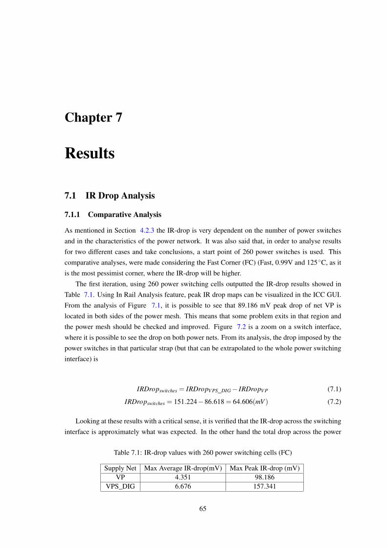
Chapter 7
Results
7.1 IR Drop Analysis
7.1.1 Comparative Analysis
As mentioned in Section 4.2.3 the IR-drop is very dependent on the number of power switches
and in the characteristics of the power network. It was also said that, in order to analyse results
for two different cases and take conclusions, a start point of 260 power switches is used. This
comparative analyses, were made considering the Fast Corner (FC) (Fast, 0.99V and 125 C, as it
is the most pessimist corner, where the IR-drop will be higher.
The first iteration, using 260 power switching cells outputted the IR-drop results showed in
Table 7.1. Using In Rail Analysis feature, peak IR drop maps can be visualized in the ICC GUI.
From the analysis of Figure 7.1, it is possible to see that 89.186 mV peak drop of net VP is
located in both sides of the power mesh. This means that some problem exits in that region and
the power mesh should be checked and improved. Figure 7.2 is a zoom on a switch interface,
where it is possible to see the drop on both power nets. From its analysis, the drop imposed by the
power switches in that particular strap (but that can be extrapolated to the whole power switching
interface) is
IRDropswitches = IRDropV PS_DIG − IRDropV P (7.1)
IRDropswitches = 151.224−86.618 = 64.606(mV ) (7.2)
Looking at these results with a critical sense, it is verified that the IR-drop across the switching
interface is approximately what was expected. In the other hand the total drop across the power
Table 7.1: IR-drop values with 260 power switching cells (FC)
Supply Net Max Average IR-drop(mV) Max Peak IR-drop (mV)VP 4.351 98.186
VPS_DIG 6.676 157.341
65
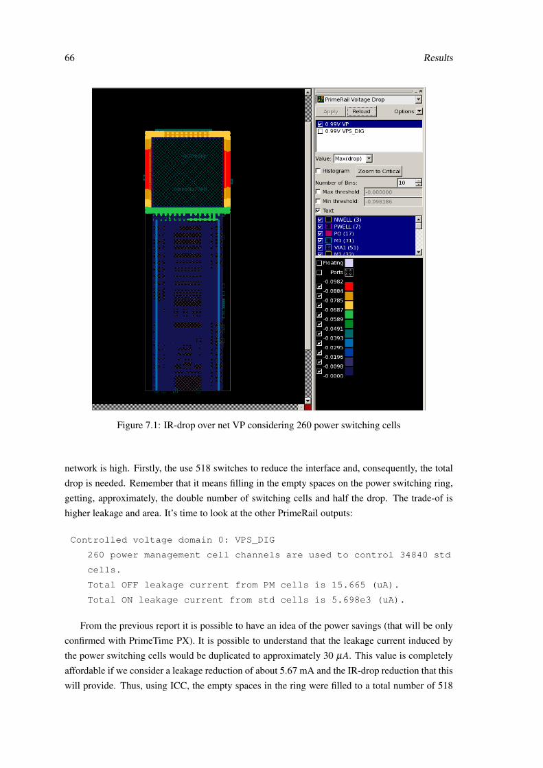
66 Results
Figure 7.1: IR-drop over net VP considering 260 power switching cells
network is high. Firstly, the use 518 switches to reduce the interface and, consequently, the total
drop is needed. Remember that it means filling in the empty spaces on the power switching ring,
getting, approximately, the double number of switching cells and half the drop. The trade-of is
higher leakage and area. It’s time to look at the other PrimeRail outputs:
Controlled voltage domain 0: VPS_DIG
260 power management cell channels are used to control 34840 std
cells.
Total OFF leakage current from PM cells is 15.665 (uA).
Total ON leakage current from std cells is 5.698e3 (uA).
From the previous report it is possible to have an idea of the power savings (that will be only
confirmed with PrimeTime PX). It is possible to understand that the leakage current induced by
the power switching cells would be duplicated to approximately 30 µA. This value is completely
affordable if we consider a leakage reduction of about 5.67 mA and the IR-drop reduction that this
will provide. Thus, using ICC, the empty spaces in the ring were filled to a total number of 518

7.1 IR Drop Analysis 67
Figure 7.2: IR-drop imposed by the 260 power switching cells
power switching cells. Besides the insertion of more power switching cells, the power network
was checked and improved. Missing vias were added and, to improve IR-drop on both sides,
of the power mesh, some extra power straps were created. Also, the power connection between
PHYGNRXAFE and rxlanedig was improved with more power straps.
7.1.2 Final Results
Table 7.2 shows the improved results for the FC, also considering the voltage rise in the net GD.
Table 7.2: IR-drop and rise values with 518 power switching cells (FC)
Supply Net Max Average IR-drop (mV) Max Peak IR-drop (mV)VP 1.489 43.116
VPS_DIG 2.534 70.996GD 1.225 (rise) 39.653 (rise)
Effective 2,714 102.255

68 Results
Figure 7.3: IR-drop over net VP considering 518 power switching cells
These final results are much better. The average drop is quite acceptable and the peak value
has decreased 86.345 mV, due to the power mesh changes and the use of more power switches.
From the map showed in Figure 7.3, it is possible to validate that the IR-drop over net VP has
improved on the sides of the power mesh, due to the inserted power straps. Figure 7.4 shows that
the drop over VPS_DIG net has its worst value in the rxlanedig logic, as expected.
From Equation 7.1 and Figure 7.5 the drop across the power switching cells is
IRDropswitches = 64.4882−42.1595 = 22.3287(mV ) (7.3)
As expected, IRDropswitches decreased in approximately 50%.
Having a final power mesh and final number of power switching cells, the analysis for the
TYPC (typical, 0.9, 25 C) and SC (slow, 0.81 , -40 C) were made. Net IR-drop values for these
corners are present in Tables 7.3 and 7.3, respectively.
Finnaly, Table 7.5 presents IR-drop across the power switching cell for all corners. Note the
biggest IR-drop across the power switches for the SC. This may seem an error because, for the

7.1 IR Drop Analysis 69
Figure 7.4: IR-drop over net VPS_DIG considering 518 power switching cells
FC and TYPC the circuit consumes more current. However, it can be explained considering the
higher resistance for which these cells are characterized for the SC (about 1kΩ, which represents
a 700Ω increase comparatively to the FC ). Even if the average and peak currents are smaller, the
high resistance value can induce a higher drop, with more impact on the peaks.
It is worth to mention that a big effort was made with the objective of decreasing the IR-drop
as much as possible. In this section, two iterations are shown, the one corresponding to the first
(and worst) obtained values and the one corresponding to the final (and best) values. However, a
few more were made. A big number of iterations were made to understand how PrimeRail works
and its different possible analyses. A smaller number of PrimeRail runs were made to evaluate
changes in the power network. The results presented in the following sections are regarding the
final version of the power network and 518 power switching cells.
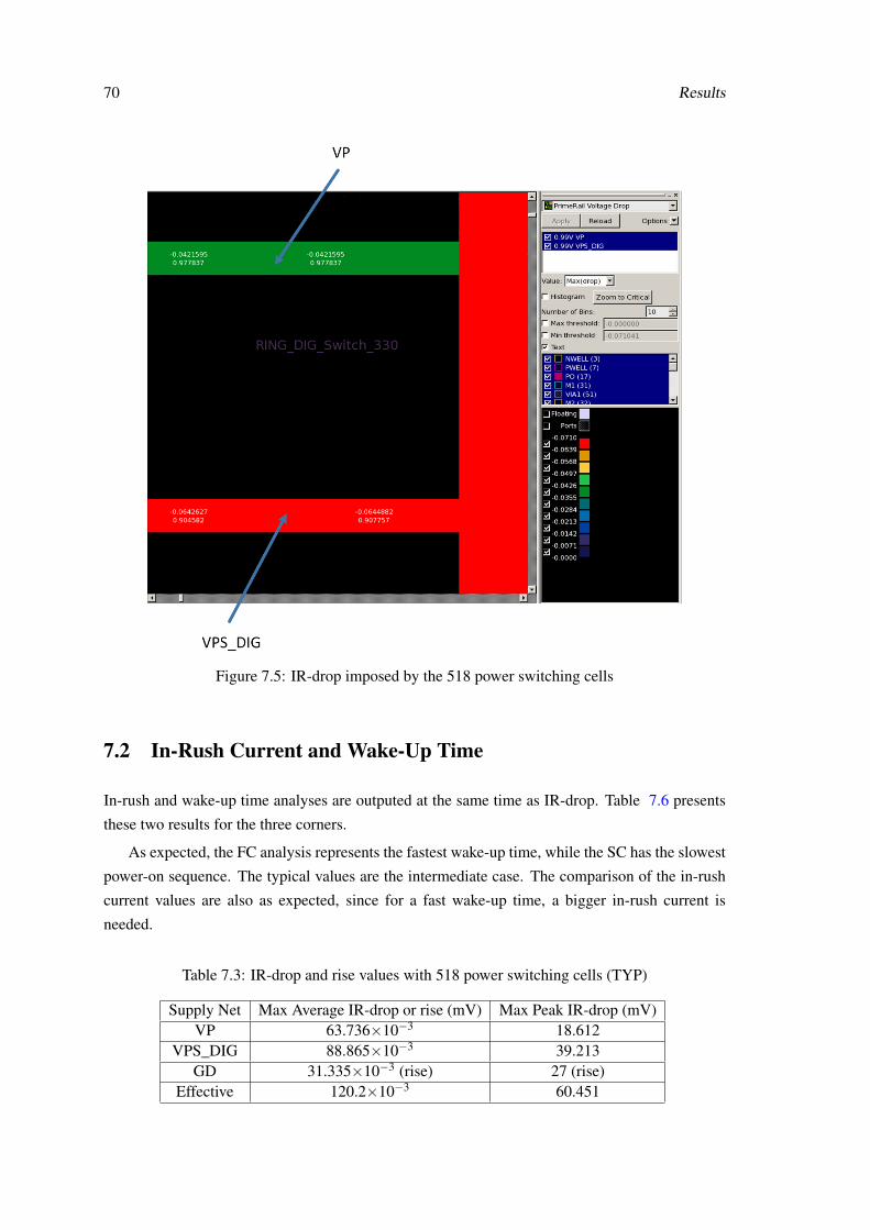
70 Results
Figure 7.5: IR-drop imposed by the 518 power switching cells
7.2 In-Rush Current and Wake-Up Time
In-rush and wake-up time analyses are outputed at the same time as IR-drop. Table 7.6 presents
these two results for the three corners.
As expected, the FC analysis represents the fastest wake-up time, while the SC has the slowest
power-on sequence. The typical values are the intermediate case. The comparison of the in-rush
current values are also as expected, since for a fast wake-up time, a bigger in-rush current is
needed.
Table 7.3: IR-drop and rise values with 518 power switching cells (TYP)
Supply Net Max Average IR-drop or rise (mV) Max Peak IR-drop (mV)VP 63.736×10⁻³ 18.612
VPS_DIG 88.865×10⁻³ 39.213GD 31.335×10⁻³ (rise) 27 (rise)
Effective 120.2×10⁻³ 60.451

7.2 In-Rush Current and Wake-Up Time 71
Table 7.4: IR-drop and rise values with 518 power switching cells (SC)
Supply Net Max Average IR-drop (mV) Max Peak IR-drop (mV)VP 36.219×10⁻³ 8.09
[1ex] VPS_DIG 112.47×10⁻³ 42.913GD 17.882×10⁻³ (rise) 11 (rise)
Effective 130.352×10⁻³ 48.519
Figure 7.6 shows the waveforms outputted by PrimeRail for the FC. It is possible to see the
generated peak current of 31.189 mA, in order to reactivate the circuit in 4.32 ns.
What needs to be evaluated is if these values don’t compromise the normal functionality of the
interface. In what concerns the wake-up time the Synopsys specifications indicate that it should
be in order of magnitude of nanoseconds, so that the interface can be quickly receiving data after a
power-on request. This way, the presented times are acceptable and were validated by Synopsys.
It also needs to be proven if the in-rush current doesn’t affect the circuits normal operation.
For that not to happen the generated peak current through the switches cannot be larger than the
current associated with the normal switching activity. PrimeRail outputted waveforms also allow
to verify this. In Figure 7.7 the first peak in both waveforms is the generated in-rush current. It
is possible to verify that it is, in fact, smaller than the sum of all currents related with the circuit
normal operation. These waveforms are also regarding the FC. For the other two corners, the same
situation happens, although with different values.
Finally, as mentioned in Section 4.2.3 the power switching cells enable pins were connected
in a daisy-chain fashion to reduce the in-rush current. In order to check what would happen if
the switches were all powered-on at the same time, a PrimeRail analysis was made considering
this scenario. The power on sequence revealed to be much faster, as expected, achieving a wake-
up time of only 441.681 (ps). But, to power the circuit in such a fast way, a in-rush current of
373.924 (mA) was generated, which would disturb the proper functionality of the interface. To
get this type of analysis done, the enable signals switching activity cannot be provided. Instead, a
VCD file can be used with the other nets switching activity annotation and, in the in-rush mode,
PrimeRail will a create a default file called .default_pm_event with the power-up sequence.
This default sequence wakes-up the power switches all at once. These results validate the need of
a daisy-chained power-on sequence.
Table 7.5: IR-drop across the power switching cells
Corner Max Average IR-drop (mV) Max Peak IR-drop (mV)FC 0.98 22.3287
TYPC 13×10-3 17SC 71.05×10⁻³ 33,43

72 Results
Table 7.6: In-Rush Current and Wake-Up Time
Corner In-rush Current (mA) Wake-up time (ns)FC 31.189 4.32
TYPC 13.939 8.202SC 7.701 11.918
7.3 Area overhead
Table 7.7 presents area and cell number results for this implementation. An additional number
of 522 cells, corresponding to 518 power switching cells and 4 SQUELCH control related cells
was introduced. This increase in the number of cells has a reflection in the total cell area and gate
count. The biggest overhead concerns the floorplan area which has increased almost 30%. This
considerably high extra area is due to the use of a ring approach and the needed space for creating
the new power network. There is, also a considerable unused area on both sides of PHYGNRXAFE
for integration purposes. Each RX lane can be integrated with more lanes, which makes impossible
the use of irregular polygons when abutting. This is a very particular issue of this implementation.
7.4 Functionality and Performance Impact
One of the goals of this dissertation is to preserve the interface functionality. To verify this re-
quirement two types of simulations were done using Synopsys VCS tool, which are described in
the following sections.
7.4.1 Post-layout simulation
This simulation has the objective to validate the proper SQUELCH control and the data reception
activity. This way a testbench is used, which instantiates PHYGNRX, and one TX lane for data
exchange. It is also important to mention that the inputs for this type of simulation are the post-
layout netlist, the verilog description of the standard cells and the SDF delay information. Figure
7.8 shows the simulation waveforms.
Initially, RX_SQ_CTR_SOC has the logic value "0", while RXDP shows a reception of data.
Then, it is changed to "1" and the HIBERNATE mode is activated, at the same time, that RX_SQ_ON_SOC
is asserted to activate the SQUELCH functionality and the monitoring of RX_SQ_OUT signal. Dur-
ing this frame the RXDP line is at DIF-Z, as explained in Chapter 3. When, the SQUELCH block
Table 7.7: Area and cell number results
Characteristic Original Power gated Overhead (%)Number of cells 21019 21541 2.48
Cell area (excluding AFE) 22297.032258 µm2 23828.08073 µm2 6.87Gate count ( total_cell_area
area_nand1 ) 43464 46448 6.42Total floorplan area (including AFE) 114300 µm2 148500 µm2 29.9
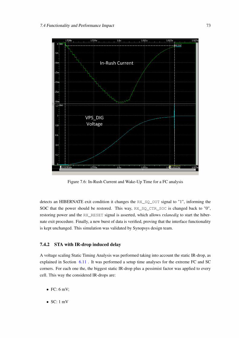
7.4 Functionality and Performance Impact 73
Figure 7.6: In-Rush Current and Wake-Up Time for a FC analysis
detects an HIBERNATE exit condition it changes the RX_SQ_OUT signal to "1", informing the
SOC that the power should be restored. This way, RX_SQ_CTR_SOC is changed back to "0",
restoring power and the RX_RESET signal is asserted, which allows rxlanedig to start the hiber-
nate exit procedure. Finally, a new burst of data is verified, proving that the interface functionality
is kept unchanged. This simulation was validated by Synopsys design team.
7.4.2 STA with IR-drop induced delay
A voltage scaling Static Timing Analysis was performed taking into account the static IR-drop, as
explained in Section 6.11 . It was performed a setup time analyses for the extreme FC and SC
corners. For each one the, the biggest static IR-drop plus a pessimist factor was applied to every
cell. This way the considered IR-drops are:
• FC: 6 mV;
• SC: 1 mV

74 Results
Figure 7.7: In-Rush Current versus the sum of all current sources
In what concerns to results, for both corners the constraints are still met. Table 7.8 summarizes
this STA results for a timing path, in order to make a comparative analysis. The STA reports are
shown in Appendixes B and C. In what concerns an hold time analysis, the timing slacks are even
better, since the circuit is slower.
Considering this analysis, although a small impact on performance is verified, the timing con-
straints are still met, which means that the functionality is not compromised.
Figure 7.8: Post-layout simulation waveforms

7.5 Power Consumption 75
Table 7.8: IR-drop induced delay for a timing path (setup analysis)
Corner Original Timing Slack (ps) Actual Timing Slack (ps) Induced Delay (ps)FC 977.5 966.3 11.2SC 48.7 33.82 14.88
7.4.3 Co-simulation
A co-simulation is a mixed-signal simulation which takes as inputs the following data:
• Verilog netlist and parasitics information for the digital simulation, which is done by Syn-
opsys VCS.
• CDL spice netlist for analogue simulation, which is done by Synopsys XA;
The co-simulation is started by VCS, which, in turn, invokes XA. This type of simulation
objective is to take power aspects into account and check if the system, in its whole, is working
and properly powered. Two co-simulations with different objectives were made and are depicted
in the following sub-sections.
7.4.3.1 Power gating simulation
This simulation has the objective of checking the proper power gating functionality, when the
RX_SQ_CTR_SOC is asserted. Figure 7.9 shows the VPS_DIG net discharging and charging con-
troled by RX_SQ_CTR_SOC. It is also represented the RX_SQ_ACK_SOC signal. This simulation,
done for the TYPC validates the proper power gating functionality.
Additionally, Figure 7.10 is a zoom on the VPS_DIG charging time, showing that the wake-up
time matches the one verified by PrimeRail in Section 7.2.
7.4.3.2 Peak simulation
This is a more precise simulation to verify if the peak currents and voltage drops verified in the
VPS_DIG net wont affect the data sampling by the flip-flops. The current and drop peaks are
associated with the switching activity and the clock transitions, making the flip-flops the most
critical cells. The waveform, considering the extreme corners (FC and SC) are shown in Figures
7.11 and 7.12. It is verified that, with these peak current and voltage drop values the flip-flops are
still capable of sampling data, thus validating the STA described in Section 7.4.2.
7.5 Power Consumption
This section presents the power consumption of the final power gated interface. First, the leak-
age savings for the Hibernate mode are shown. Then, the impact in HS-mode and LS-mode is
analysed.

76 Results
Figure 7.9: Co-simulation for power gating validation
From Table 7.9, it is possible to understand that high leakage savings are achieved for Hiber-
nate mode, which confirms Power Gating as a very effective low power technique. As expected the
FC presents the highest savings, since leakage grows with temperature and speed. Having anal-
ysed the leakage savings, it is interesting to see where does the remaining leakage comes from.
Table 7.10 shows the leakage consumption by design element. It is possible to verify that the a
big part still comes from rxlanedig which indicates that the power switches Io f f current is also
inducing leakage power consumption by rxlanedig, thus it is not possible to completely shut down
that power domain.
The benefits of power gating are evident when the Hibernate mode is considered. However,
in HS-mode and LS-mode, the extra power switching cells and multiplexer cells induce an extra
power consumption, in both dynamic and leakage power. This negative impact, shown in Tables
7.11 and 7.12 is small and acceptable when such higher power reduction is obtained for Hibernate
mode by power gating the design. It is certain, though, that the ratio between what is gained and
Table 7.9: Leakage Power Consumption and savings
CornerLeakage Power
Original Power Gated Savings (%)FC 5.77 mW 27.9 µW 99.51TYPC 31.4 µW 1.92 µW 93.89SC 1.25 µW 288 nW 76.96

7.5 Power Consumption 77
Figure 7.10: Co-simulation and wake-up time
lost, depends a lot on the application of this interface. In a normal application, the most likely
situation is having long periods of hibernating, intercalated with small periods of bursty activity,
which makes the power reduction considerably high.

78 Results
Figure 7.11: Co-simulation for the FC
Table 7.10: Leakage Power by elements
Corner Element Leakage Power %
FCrxlanedig 10.9 µW 39
Switches and multiplexers 17 µW 61PHYGNRX (total) 27.9 µW 100
TYPCrxlanedig 1.80 µW 93.75
Switches and multiplexers 0.12 µW 6.25PHYGNRX (total) 1.92 µ W 100
SCrxlanedig 272 nW 94.4
Switches and multiplexers 16 nW 5.6PHYGNRX (total) 288 nW 100

7.5 Power Consumption 79
Figure 7.12: Co-simulation for the SC
Table 7.11: Power Impact in HS-mode
Corner Power consumption Original Power Gated Increase (%)Dynamic power 5.64 mW 5.74 mW 1.77
FC Leakage power 5.88 mW 5.90 mW 0.34Total power 11.52 mW 11.64 mW 1.04
Dynamic power 4.33 mW 4.39 mW 1.39TYPC Leakage power 32 µW 32.3 µW 0.94
Total power 4.362 mW 4.4223 mW 1.38Dynamic power 3.27 mW 3.36 mW 2.75
SC Leakage power 1.25 µW 1.31 µW 4.8Total power 3.27125 mW 3.36131 mW 2.75

80 Results
Table 7.12: Power Impact in LS-mode
Corner Power consumption Original Power Gated Increase (%)Dynamic power 188.9 µW 189.7 µW 0.42
FC Leakage power 5.8 mW 5.82 mW 0.34Total power 5.9889 mW 6.01 mW 0.35
Dynamic power 144.7 µW 145.4 µW 0.48TYPC Leakage power 31.6 µW 31.8 µW 0.63
Total power 176.3 µW 177.2 µW 0.51Dynamic power 112.6 µW 113.3 µW 0.62
SC Leakage power 1.25 µW 1.31 µW 4.8Total power 113.85 µW 114.61 µW 0.67

Chapter 8
Conclusion
8.1 Final Conclusions
In this dissertation the low power technique Power Gating is implemented on the RX lane of a
state-of-the-art Synopsys interface, designed with the 28nm advanced technology process. Work-
ing in the industry environment and using Synopsys toolset, the standard design flow was learned
and adapted to allow a power gating implementation, being covered from the beginning to the end.
Initially, a research was made to understand the basic concepts that are present in a power
gating implementation. The definitions of power and energy was explained in order to understand
their difference. The power gating principle of operation was depicted and it was understood that
a digital chip or parts of it may be powered down when in idle state to reduce power. The main
element of a power gating implementation is the power switch. It is powered by the permanent
supply net and delivers power the the controlled elements. These switches can be placed in a ring
or array style.
Then, after the introduction of the standard design flow, it was explained that in order to apply
power gating the UPF standard can be used throughout the entire flow to describe the power
intent of the chip, complementing the RTL description. Synopsys tools understand the constructs
defined in an UPF file and allow implementing, optimizing and analysing a chip with low power
characteristics. The main constructs of an UPF specification are: power domains; supply nets and
ports; power switches; power state tables and, eventually, retention registers and isolation cells.
The core of this dissertation is the implementation itself described in Chapter 6. For every
flow stage the main issues in a power gating implementation are explained, considering the use of
header switches and ring implementation without the use of retention registers and isolation cells.
First, the power intent needs to be described using the UPF syntax. Then, it is important to ensure
that any interfacing signal of the power gated block that is still provided to other blocks as the
SQUELCH control signal for the PHYGNRXAFE.
The design libraries creation and management can be a challenge. There is a great amount of
data that needs to be taken care of and logic libraries compliant with the Liberty PG Pin Syntax
needs to be available. It is also needed a library containing power switching cells.
81

82 Conclusion
The synthesis step is simple. It is responsible to translate the RTL description into a gate-level
netlis, but also to infer special cells from the UPF description. In this implementation those cells
are not present, so, the synthesis process is similar to the standard. Formal equivalence using
Formality accepts the UPF standard and considers all possible power states.
The bigger part of the implementation and, so, the biggest changes are in the Place&Route
stage using IC Compiler. Among these changes it is possible to distinguish:
• The creation of voltage areas taking into account the power domains specified in the UPF
file;
• The automatic logic connection of supply pins to the power domains primary power and
primary ground nets, which are, again, defined in the UPF file;
• The power switching ring insertion and respective enable/control pins connection in a daisy-
chain fashion in order to minimize the in-rush current. In what concerns to the number of
power switches to insert the best approach is to use an iterative process, with an appropriate
start point, and see what best fits the design needs.
• The power network creation for two distinct supply regions. A normal power mesh in upper
metals can be used in the always-on side, while a strong ring can power the controlled
domain. At this point was concluded that the interface represented by the power switches
is very important for IR drop purposes. In order to minimize it the power straps should be
aligned with its pins and connected directly through vias.
The sign of analyses tools flow also presents changes. Although minimal, these changes allow
to proper analyse the design. PrimeTime uses the UPF to build a virtual network and annotate each
standard cell pin voltage. PrimeRail revealed to be the most tricky tool but allows to perform very
complete and exhaustive analyses. It needs a CONN view of the analogue block to understand
its power network. Using the UPF power intent it understands what power domains exist, as
well as nets and pin voltages. With this information it performs, IR-drop, in-rush and wake up
time analyses, providing, as well, information about the power consumption and what are the
possible gains. In turn, PrimeTime PX is the sign-off power analysis Synopsys tool. It recognizes
the switches ON/OFF states from the UPF file and the annotated value of the respective nets,
generating detailed power reports.
The dissertation goals where achieved, meaning that:
• A power reduction up to 99.51% was achieved for the Hibernate mode;
• The interface functionality was not affected;
• An adapted design flow was applied and fully covered;
• The negative impact of a power gating implementation in aspects like performance, area,
extra leakage from the switches or ir-drop was understood. The biggest impact is on the
physical area (29.9%) due to the use of a ring approach.

8.2 Future Work 83
Finally, some words in the first person. I found this dissertation to be very challenging, but with
a great personal satisfaction level. I can, certainly, say that I almost started form ground zero and in
a short period of time I have learnt more than could ever imagine. It allowed me to consolidate and
improve my knowledge in what concerns VLSI design and low-power methodologies, working
with such complex tools like the Synopsys toolset is. The most challenging part turned out to be,
indeed, the best part too: The adaptation to an industrial environment.
8.2 Future Work
In this final section, it is presented a possible expansion of the work here described:
• Power gating individual blocks inside the rxlanedig IP.
Notwithstanding the good results, this implementation only allows to save power for one
operating mode. With the gained knowledge, it is possible, now, to identify and power gate
individual blocks in a lower hierarchy level, thus saving power in other operating modes.
Considering that implementation, an array approach could be explored, as well as the use
of special cells, such as, retention registers and isolation cells. Thereby, it would allow to
further explore Design Compiler capabilities for low power implementations. It will also
have less impact on area.

84 Conclusion

Appendix A
UPF specification for the FC
Below is the UPF specification for this implementation, considering the FC. Section 6.3 explains
its construction.
#Power Domains
create_power_domain TOP
create_power_domain PD_DIG -elements rxlanedig
create_power_domain PD_AFE -elements PHYGNRXAFE
#Suplly Nets
create_supply_net VP -domain TOP
create_supply_net VP -domain PD_AFE -reuse
create_supply_net VPH -domain PD_AFE
create_supply_net -domain TOP -reuse VPH
create_supply_net VPS_DIG -domain PD_DIG
create_supply_net VPS_DIG -domain TOP -reuse
create_supply_net GD -domain TOP
create_supply_net GD -domain PD_DIG -reuse
create_supply_net GD -domain PD_AFE -reuse
#Supply Ports
create_supply_port VP
create_supply_port GD
create_supply_port VPH
Supple Nets/Ports Connection
85

86 UPF specification for the FC
connect_supply_net VP -ports VP
connect_supply_net VPH -ports VPH
connect_supply_net VPH -ports PHYGNRXAFE/vph
connect_supply_net GD -ports GD
#Set Domain Primary Supplies
set_domain_supply_net TOP
-primary_power_net VP
-primary_ground_net GD
set_domain_supply_net PD_DIG
-primary_power_net VPS_DIG
-primary_ground_net GD
set_domain_supply_net PD_AFE
-primary_power_net VP
-primary_ground_net GD
connect_supply_net VPH -ports I01MPHYGNRXAFETYPE1/vph
#Power Switch
create_power_switch PD_DIG_SW
-domain TOP
-input_supply_port VDDP VP
-output_supply_port VDDC VPS_DIG
-control_port RX_SQ_CTR_SOC RX_SQ_CTR_SOC
-ack_port RX_SQ_ACK_SOC RX_SQ_ACK_SOC
-on_state on_state VDDP !RX_SQ_CTR_SOC
#Port States
add_port_state VP -state TOP_VP 0.99
add_port_state GD -state GND 0.0
add_port_state PD_DIG_SW/VDDC
-state POWER_ON 0.99
-state POWER_OFF off
add_port_state VPH -state TOP_VPH 1.98

UPF specification for the FC 87
#Power State Table
create_pst PST -supplies VP VPS_DIG GD VPH
add_pst_state ON -pst PST -state TOP_VP POWER_ON GND TOP_VPH
add_pst_state OFF -pst PST -state TOP_VP POWER_OFF GND TOP_VPH

88 UPF specification for the FC

Appendix B
STA Reports for FC
This appendix presents the Voltage Scaling STA reports (FC) for a setup time analysis, which
allows to see the delay induced by IR drop. The summary results are presented in Section 7.4.2.
B.1 STA report discarding IR-Drop
****************************************
Report : timing
-path_type full_clock_expanded
-delay_type max
-max_paths 1
Design : PHYGNRX
Version: G-2012.06-SP3
****************************************
Startpoint: rxlanedig/rxwideifxdiv_clk_regx0x/Q
(clock source ’hswclkdiv2’)
Endpoint:rxlanedig/rxwideifxdiv_clk_regx1x
(rising edge-triggered flip-flop clocked by pointer_clk’)
Path Group: pointer_clk
Path Type: max
Point Incr Path Voltage
-----------------------------------------------------------
clock hswclkdiv2 (fall edge)
2.0250 2.0250
clock pointer_clk (source latency)
0.0000 2.0250
rxlanedig/rx_pointer_clk (mrxlanedig)
0.0000 2.0250 f 0.9900
89

90 STA Reports for FC
rxlanedig/rxafectrlxhand_mux_scan_anapins_rx_pointer_clk_outxU1/X (MUX2_S_4)
0.0228 & 2.0478 f 0.9900
rxlanedig/U316/X (INV_S_6)
0.0099 & 2.0577 r 0.9900
rxlanedig/hand_pointerclk_muxxU2/X (MUX2_S_4)
0.0309 & 2.0886 r 0.9900
rxlanedig/hand_pointerclk_muxxU1/X (BUF_S_8)
0.0220 & 2.1106 r 0.9900
rxlanedig/eco_cell_22_0/X (DEL_L6_8)
0.1460 & 2.2566 r 0.9900
rxlanedig/rxwideifxhand_inclk_gatexhand_clk_gate_orxU1/X (OR2_6)
0.0197 & 2.2763 r 0.9900
rxlanedig/rxwideifxhand_inclk_scan_muxxU1/X (MUX2_S_4)
0.0213 & 2.2976 r 0.9900
rxlanedig/rxwideifxdiv_clk_regx0x/Q (FSDPSBQ_V2_4) (gclock source)
0.0633 & 2.3609 f 0.9900
rxlanedig/rxwideifxdiv_clk_regx0x/Q (FSDPSBQ_V2_4)
0.0000 2.3609 f 0.9900
rxlanedig/rxwideifxU158/X (OAI221_1)
0.0157 & 2.3766 r 0.9900
rxlanedig/U5335/X (DEL_L4_1)
0.0597 & 2.4363 r 0.9900
rxlanedig/rxwideifxdiv_clk_regx1x/D (FSDPSBQ_V2_4)
0.0000 & 2.4363 r 0.9900
data arrival time 2.4363
clock pointer_clk’ (rise edge)
3.3750 3.3750
clock source latency 0.0000 3.3750
rxlanedig/rx_pointer_clk (mrxlanedig)
0.0000 3.3750 f 0.9900
rxlanedig/rxafectrlxhand_mux_scan_anapins_rx_pointer_clk_outxU1/X (MUX2_S_4)
0.0226 & 3.3976 f 0.9900
rxlanedig/U316/X (INV_S_6)
0.0097 & 3.4073 r 0.9900
rxlanedig/hand_pointerclk_muxxU2/X (MUX2_S_4)
0.0308 & 3.4381 r 0.9900
rxlanedig/hand_pointerclk_muxxU1/X (BUF_S_8)
0.0220 & 3.4601 r 0.9900
rxlanedig/eco_cell_22_0/X (DEL_L6_8)
0.1456 & 3.6057 r 0.9900
rxlanedig/rxwideifxhand_inclk_gatexhand_clk_gate_orxU1/X (OR2_6)
0.0194 & 3.6252 r 0.9900
rxlanedig/rxwideifxhand_inclk_scan_muxxU1/X (MUX2_S_4)
0.0211 & 3.6463 r 0.9900

B.2 STA report considering IR-Drop 91
rxlanedig/rxwideifxdiv_clk_regx1x/CK (FSDPSBQ_V2_4)
0.0000 & 3.6463 r 0.9900
clock uncertainty -0.2000 3.4463
library setup time -0.0325 3.4138
data required time 3.4138
-----------------------------------------------------------
data required time 3.4138
data arrival time -2.4363
-----------------------------------------------------------
slack (MET) 0.9775
B.2 STA report considering IR-Drop
****************************************
Report : timing
-path_type full_clock_expanded
-delay_type max
-max_paths 1
Design : PHYGNRX
Version: G-2012.06-SP3
****************************************
Startpoint: rxlanedig/rxwideifxdiv_clk_regx0x/Q
(clock source ’hswclkdiv2’)
Endpoint: rxlanedig/rxwideifxdiv_clk_regx1x
(rising edge-triggered flip-flop clocked by pointer_clk’)
Path Group: pointer_clk
Path Type: max
Point Incr Path Voltage
-----------------------------------------------------------
clock hswclkdiv2 (fall edge)
2.0250 2.0250
clock pointer_clk (source latency)
0.0000 2.0250
rxlanedig/rx_pointer_clk (mrxlanedig)
0.0000 2.0250 f 0.9900
rxlanedig/rxafectrlxhand_mux_scan_anapins_rx_pointer_clk_outxU1/X (MUX2_S_4)
0.0241 & 2.0491 f 0.9840
rxlanedig/U316/X (INV_S_6)
0.0101 & 2.0592 r 0.9840
rxlanedig/hand_pointerclk_muxxU2/X (MUX2_S_4)
0.0322 & 2.0914 r 0.9840

92 STA Reports for FC
rxlanedig/hand_pointerclk_muxxU1/X (BUF_S_8)
0.0225 & 2.1139 r 0.9840
rxlanedig/eco_cell_22_0/X (DEL_L6_8)
0.1583 & 2.2723 r 0.9840
rxlanedig/rxwideifxhand_inclk_gatexhand_clk_gate_orxU1/X (OR2_6)
0.0205 & 2.2928 r 0.9840
rxlanedig/rxwideifxhand_inclk_scan_muxxU1/X (MUX2_S_4)
0.0225 & 2.3153 r 0.9840
rxlanedig/rxwideifxdiv_clk_regx0x/Q (FSDPSBQ_V2_4) (gclock source)
0.0676 & 2.3829 f 0.9840
rxlanedig/rxwideifxdiv_clk_regx0x/Q (FSDPSBQ_V2_4)
0.0000 2.3829 f 0.9840
rxlanedig/rxwideifxU158/X (OAI221_1)
0.0164 & 2.3993 r 0.9840
rxlanedig/U5335/X (DEL_L4_1)
0.0635 & 2.4628 r 0.9840
rxlanedig/rxwideifxdiv_clk_regx1x/D (FSDPSBQ_V2_4)
0.0000 & 2.4628 r 0.9840
data arrival time 2.4628
clock pointer_clk’ (rise edge)
3.3750 3.3750
clock source latency 0.0000 3.3750
rxlanedig/rx_pointer_clk (mrxlanedig)
0.0000 3.3750 f 0.9900
rxlanedig/rxafectrlxhand_mux_scan_anapins_rx_pointer_clk_outxU1/X (MUX2_S_4)
0.0239 & 3.3989 f 0.9840
rxlanedig/U316/X (INV_S_6)
0.0099 & 3.4088 r 0.9840
rxlanedig/hand_pointerclk_muxxU2/X (MUX2_S_4)
0.0321 & 3.4409 r 0.9840
rxlanedig/hand_pointerclk_muxxU1/X (BUF_S_8)
0.0225 & 3.4635 r 0.9840
rxlanedig/eco_cell_22_0/X (DEL_L6_8)
0.1579 & 3.6213 r 0.9840
rxlanedig/rxwideifxhand_inclk_gatexhand_clk_gate_orxU1/X (OR2_6)
0.0203 & 3.6416 r 0.9840
rxlanedig/rxwideifxhand_inclk_scan_muxxU1/X (MUX2_S_4)
0.0223 & 3.6639 r 0.9840
rxlanedig/rxwideifxdiv_clk_regx1x/CK (FSDPSBQ_V2_4)
0.0000 & 3.6639 r 0.9840
clock uncertainty -0.2000 3.4639
library setup time -0.0348 3.4291
data required time 3.4291
-----------------------------------------------------------

B.2 STA report considering IR-Drop 93
data required time 3.4291
data arrival time -2.4628
-----------------------------------------------------------
slack (MET) 0.9663

94 STA Reports for FC

Appendix C
STA Reports for SC
This appendix presents the Voltage Scaling STA reports (SC) for a setup time analysis, which
allows to see the delay induced by IR drop. The summary results are presented in Section 7.4.2.
C.1 STA report discarding IR-Drop
****************************************
Report : timing
-path_type full_clock_expanded
-delay_type max
-max_paths 1
Design : PHYGNRX
Version: G-2012.06-SP3
****************************************
Startpoint: rxlanedig/rxwideifxrx_phydordy_out_latch_regx2x
(rising edge-triggered flip-flop clocked by pointer_clk’)
Endpoint: rxlanedig/rx_phydordy_regx2x
(rising edge-triggered flip-flop clocked by symbolclkhs_incg’)
Path Group: symbolclkhs_incg
Path Type: max
Point Incr Path Voltage
-----------------------------------------------------------
clock pointer_clk’ (rise edge)
0.6750 0.6750
clock source latency 0.0000 0.6750
rxlanedig/rx_pointer_clk (mrxlanedig)
0.0000 0.6750 f 0.8100
rxlanedig/rxafectrlxhand_mux_scan_anapins_rx_pointer_clk_outxU1/X (MUX2_S_4)
95
96 STA Reports for SC
0.0649 & 0.7399 f 0.8100
rxlanedig/U316/X (INV_S_6)
0.0296 & 0.7695 r 0.8100
rxlanedig/hand_pointerclk_muxxU2/X (MUX2_S_4)
0.0967 & 0.8662 r 0.8100
rxlanedig/hand_pointerclk_muxxU1/X (BUF_S_8)
0.0607 & 0.9269 r 0.8100
rxlanedig/eco_cell_20_0/X (DEL_L6_8)
0.6429 & 1.5699 r 0.8100
rxlanedig/BUF_S_12_G1B1I1_3/X (BUF_S_12)
0.0982 & 1.6681 r 0.8100
rxlanedig/BUF_S_12_G1B2I3_3/X (BUF_S_12)
0.0588 & 1.7269 r 0.8100
rxlanedig/BUF_S_8_G1B3I19/X (BUF_S_8)
0.0606 & 1.7875 r 0.8100
rxlanedig/rxwideifxrx_phydordy_out_latch_regx2x/CK (FSDPRBQ_D_2)
0.0014 & 1.7889 r 0.8100
rxlanedig/rxwideifxrx_phydordy_out_latch_regx2x/Q (FSDPRBQ_D_2)
0.0981 & 1.8870 f 0.8100
rxlanedig/U3840/X (BUF_D_8)
0.0415 & 1.9285 f 0.8100
rxlanedig/U7334/X (BUF_8)
0.0264 & 1.9549 f 0.8100
rxlanedig/U8979/X (BUF_12)
0.0226 & 1.9774 f 0.8100
rxlanedig/U256/X (OR2_1)
0.0937 & 2.0711 f 0.8100
rxlanedig/U9139/X (BUF_2)
0.0463 & 2.1173 f 0.8100
rxlanedig/U10068/X (DEL_L4_4)
0.1971 & 2.3144 f 0.8100
rxlanedig/U9138/X (BUF_8)
0.0379 & 2.3524 f 0.8100
rxlanedig/U10458/X (DEL_L6_1)
0.6168 & 2.9691 f 0.8100
rxlanedig/U6485/X (BUF_4)
0.0816 & 3.0508 f 0.8100
rxlanedig/eco_cell_53_0/X (DEL_L4_1)
0.2151 & 3.2659 f 0.8100
rxlanedig/eco_cell_75_0/X (BUF_12)
0.0401 & 3.3060 f 0.8100
rxlanedig/rx_phydordy_regx2x/D (FSDPRBQ_D_2)
0.0000 & 3.3061 f 0.8100
data arrival time 3.3061

C.1 STA report discarding IR-Drop 97
clock symbolclkhs_incg’ (rise edge)
2.0250 2.0250
clock pointer_clk (source latency)
0.0000 2.0250
rxlanedig/rx_pointer_clk (mrxlanedig)
0.0000 2.0250 f 0.8100
rxlanedig/rxafectrlxhand_mux_scan_anapins_rx_pointer_clk_outxU1/X (MUX2_S_4)
0.0648 & 2.0898 f 0.8100
rxlanedig/U316/X (INV_S_6)
0.0295 & 2.1194 r 0.8100
rxlanedig/hand_pointerclk_muxxU2/X (MUX2_S_4)
0.0966 & 2.2160 r 0.8100
rxlanedig/hand_pointerclk_muxxU1/X (BUF_S_8)
0.0607 & 2.2767 r 0.8100
rxlanedig/eco_cell_22_0/X (DEL_L6_8)
0.6122 & 2.8889 r 0.8100
rxlanedig/rxwideifxhand_inclk_gatexhand_clk_gate_orxU1/X (OR2_6)
0.0847 & 2.9736 r 0.8100
rxlanedig/rxwideifxU156/X (INV_S_6)
0.0150 & 2.9886 f 0.8100
rxlanedig/rxwideifxU289/A3 (OAI32_4) (gclock source)
0.0002 & 2.9887 f 0.8100
rxlanedig/rxwideifxU289/X (OAI32_4)
0.0379 & 3.0267 r 0.8100
rxlanedig/rxwideifxU153/X (OAO211_DG_4)
0.0469 & 3.0736 r 0.8100
rxlanedig/hand_symbolclkhs_scan_muxxU1/X (MUX2_S_4)
0.0742 & 3.1478 r 0.8100
rxlanedig/BUF_S_8_G1IP_8/X (BUF_S_8)
0.0428 & 3.1906 r 0.8100
rxlanedig/hand_symbolclkhs_gatexhand_clk_gate_orxU1/X (OR2_6)
0.0299 & 3.2205 r 0.8100
rxlanedig/hand_symbolclk_muxxU1/X (MUX2_S_4)
0.0613 & 3.2819 r 0.8100
rxlanedig/hand_outclk_scan_muxxU2/X (MUX2_S_4)
0.0830 & 3.3649 r 0.8100
rxlanedig/hand_outclk_scan_muxxU1/X (BUF_S_8)
0.0407 & 3.4055 r 0.8100
rxlanedig/eco_cell_19_1/X (BUF_S_2)
0.0431 & 3.4487 r 0.8100
rxlanedig/eco_cell_19_0/X (BUF_S_2)
0.0888 & 3.5374 r 0.8100
rxlanedig/BUF_S_8_G1B1I5_7/X (BUF_S_8)
0.0929 & 3.6304 r 0.8100
rxlanedig/rx_phydordy_regx2x/CK (FSDPRBQ_D_2)

98 STA Reports for SC
0.0007 & 3.6311 r 0.8100
clock uncertainty -0.1500 3.4811
library setup time -0.1263 3.3548
data required time 3.3548
-----------------------------------------------------------
data required time 3.3548
data arrival time -3.3061
-----------------------------------------------------------
slack (MET) 0.0487
C.2 STA report considering IR-Drop
****************************************
Report : timing
-path_type full_clock_expanded
-delay_type max
-max_paths 1
Design : PHYGNRX
Version: G-2012.06-SP3
****************************************
Startpoint: rxlanedig/rxwideifxrx_phydordy_out_latch_regx2x
(rising edge-triggered flip-flop clocked by pointer_clk’)
Endpoint: rxlanedig/rx_phydordy_regx2x
(rising edge-triggered flip-flop clocked by symbolclkhs_incg’)
Path Group: symbolclkhs_incg
Path Type: max
Point Incr Path Voltage
-----------------------------------------------------------
clock pointer_clk’ (rise edge)
0.6750 0.6750
clock source latency 0.0000 0.6750
rxlanedig/rx_pointer_clk (mrxlanedig)
0.0000 0.6750 f 0.8100
rxlanedig/rxafectrlxhand_mux_scan_anapins_rx_pointer_clk_outxU1/X (MUX2_S_4)
0.0658 & 0.7408 f 0.8090
rxlanedig/U316/X (INV_S_6)
0.0297 & 0.7705 r 0.8090
rxlanedig/hand_pointerclk_muxxU2/X (MUX2_S_4)
0.0976 & 0.8681 r 0.8090
rxlanedig/hand_pointerclk_muxxU1/X (BUF_S_8)
0.0611 & 0.9291 r 0.8090

C.2 STA report considering IR-Drop 99
rxlanedig/eco_cell_20_0/X (DEL_L6_8)
0.6509 & 1.5801 r 0.8090
rxlanedig/BUF_S_12_G1B1I1_3/X (BUF_S_12)
0.0986 & 1.6787 r 0.8090
rxlanedig/BUF_S_12_G1B2I3_3/X (BUF_S_12)
0.0592 & 1.7379 r 0.8090
rxlanedig/BUF_S_8_G1B3I19/X (BUF_S_8)
0.0611 & 1.7990 r 0.8090
rxlanedig/rxwideifxrx_phydordy_out_latch_regx2x/CK (FSDPRBQ_D_2)
0.0014 & 1.8004 r 0.8090
rxlanedig/rxwideifxrx_phydordy_out_latch_regx2x/Q (FSDPRBQ_D_2)
0.0992 & 1.8996 f 0.8090
rxlanedig/U3840/X (BUF_D_8)
0.0418 & 1.9414 f 0.8090
rxlanedig/U7334/X (BUF_8)
0.0265 & 1.9679 f 0.8090
rxlanedig/U8979/X (BUF_12)
0.0227 & 1.9906 f 0.8090
rxlanedig/U256/X (OR2_1)
0.0950 & 2.0856 f 0.8090
rxlanedig/U9139/X (BUF_2)
0.0466 & 2.1322 f 0.8090
rxlanedig/U10068/X (DEL_L4_4)
0.1992 & 2.3314 f 0.8090
rxlanedig/U9138/X (BUF_8)
0.0382 & 2.3696 f 0.8090
rxlanedig/U10458/X (DEL_L6_1)
0.6252 & 2.9948 f 0.8090
rxlanedig/U6485/X (BUF_4)
0.0822 & 3.0770 f 0.8090
rxlanedig/eco_cell_53_0/X (DEL_L4_1)
0.2174 & 3.2944 f 0.8090
rxlanedig/eco_cell_75_0/X (BUF_12)
0.0404 & 3.3348 f 0.8090
rxlanedig/rx_phydordy_regx2x/D (FSDPRBQ_D_2)
0.0000 & 3.3348 f 0.8090
data arrival time 3.3348
clock symbolclkhs_incg’ (rise edge)
2.0250 2.0250
clock pointer_clk (source latency)
0.0000 2.0250
rxlanedig/rx_pointer_clk (mrxlanedig)
0.0000 2.0250 f 0.8100
rxlanedig/rxafectrlxhand_mux_scan_anapins_rx_pointer_clk_outxU1/X (MUX2_S_4)

100 STA Reports for SC
0.0657 & 2.0907 f 0.8090
rxlanedig/U316/X (INV_S_6)
0.0297 & 2.1204 r 0.8090
rxlanedig/hand_pointerclk_muxxU2/X (MUX2_S_4)
0.0974 & 2.2179 r 0.8090
rxlanedig/hand_pointerclk_muxxU1/X (BUF_S_8)
0.0610 & 2.2789 r 0.8090
rxlanedig/eco_cell_22_0/X (DEL_L6_8)
0.6197 & 2.8986 r 0.8090
rxlanedig/rxwideifxhand_inclk_gatexhand_clk_gate_orxU1/X (OR2_6)
0.0852 & 2.9839 r 0.8090
rxlanedig/rxwideifxU156/X (INV_S_6)
0.0150 & 2.9989 f 0.8090
rxlanedig/rxwideifxU289/A3 (OAI32_4) (gclock source)
0.0002 & 2.9991 f 0.8090
rxlanedig/rxwideifxU289/X (OAI32_4)
0.0383 & 3.0374 r 0.8090
rxlanedig/rxwideifxU153/X (OAO211_DG_4)
0.0473 & 3.0846 r 0.8090
rxlanedig/hand_symbolclkhs_scan_muxxU1/X (MUX2_S_4)
0.0748 & 3.1594 r 0.8090
rxlanedig/BUF_S_8_G1IP_8/X (BUF_S_8)
0.0431 & 3.2026 r 0.8090
rxlanedig/hand_symbolclkhs_gatexhand_clk_gate_orxU1/X (OR2_6)
0.0301 & 3.2327 r 0.8090
rxlanedig/hand_symbolclk_muxxU1/X (MUX2_S_4)
0.0618 & 3.2945 r 0.8090
rxlanedig/hand_outclk_scan_muxxU2/X (MUX2_S_4)
0.0837 & 3.3782 r 0.8090
rxlanedig/hand_outclk_scan_muxxU1/X (BUF_S_8)
0.0409 & 3.4191 r 0.8090
rxlanedig/eco_cell_19_1/X (BUF_S_2)
0.0435 & 3.4627 r 0.8090
rxlanedig/eco_cell_19_0/X (BUF_S_2)
0.0895 & 3.5522 r 0.8090
rxlanedig/BUF_S_8_G1B1I5_7/X (BUF_S_8)
0.0936 & 3.6458 r 0.8090
rxlanedig/rx_phydordy_regx2x/CK (FSDPRBQ_D_2)
0.0007 & 3.6465 r 0.8090
clock uncertainty -0.1500 3.4965
library setup time -0.1279 3.3686
data required time 3.3686
-----------------------------------------------------------
data required time 3.3686
data arrival time -3.3348

C.2 STA report considering IR-Drop 101
-----------------------------------------------------------
slack (MET) 0.0338

102 STA Reports for SC
References
[1] ITRS Working Group. INTERNATIONAL TECHNOLOGY ROADMAP FOR SEMICON-DUCTORS: Design, 2010.
[2] Synopsys Low-Power Flow User Guide, Version F-2011.09, September 2011.
[3] Michael Keating, David Flynn, Rob Aitken, Alan Gibbons, and Kaijian Shi. Low PowerMethodology Manual: For System-on-Chip Design. Springer Publishing Company, Incorpo-rated, 2007.
[4] Ping Huang, Zuocheng Xing, Tianran Wang, Qiang Wei, Hongyan Wang, and Guitao Fu.A brief survey on power gating design. In Solid-State and Integrated Circuit Technology(ICSICT), 2010 10th IEEE International Conference on, pages 788–790, 2010.
[5] Eugene Wang. Synopsys power-gating design methodology based on smic 90nm process.
[6] Neil Weste and David Harris. CMOS VLSI Design: A Circuits and Systems Perspective.Addison-Wesley Publishing Company, USA, 4th edition, 2010.
[7] Sven Rosinger. RT-Level Power-Gating Models optimizing Dynamic Leakage-Management.PhD thesis, Carl von Ossietzky Universität Oldenburg, 2012.
[8] Nelson Silva. Power reduction of a cmos high-speed interface using clock gating. Master’sthesis, Faculdade de Engenharia da Universidade do Porto, To be published in July, 2013.
[9] D. Dal and N. Mansouri. Power optimization with power islands synthesis. Computer-AidedDesign of Integrated Circuits and Systems, IEEE Transactions on, 28(7):1025–1037, 2009.
[10] Chao-Yang Chang, Pai-Cheng Tso, Chung-Hsun Huang, and Po-Hui Yang. A fast wake-up power gating technique with inducing a balanced rush current. In Circuits and Systems(ISCAS), 2012 IEEE International Symposium on, pages 3086–3089, 2012. doi:10.1109/ISCAS.2012.6271972.
[11] Ieee standard for design and verification of low-power integrated circuits. IEEE Std 1801-2013 (Revision of IEEE Std 1801-2009), pages 1–348, 2013. doi:10.1109/IEEESTD.2013.6521327.
[12] Design Compiler User Guide, Version G-2012.06, June 2012.
[13] Synopys Multivoltage Flow User Guide, Version H-2013.03, March 2013.
[14] Library Data Preparation for IC Compiler User Guide, Version F-2011.09, September 2011.
[15] IC Compiler User Guide, Version G-2012.06-SP4, June 2012.
103

104 REFERENCES
[16] Arien Wolf. Robust Power Gating Implementatin using ICC, 2009.
[17] Implementing Power Gating Using Synopsys R© Implementation Tools Application Note, Ver-sion A-2007.12, December 2007.
[18] PrimeRail User Guide, Version G-2012.06, June 2012.
[19] PrimeTime PX User Guide Version H-2012.12, December 2012.