Embed Size (px)
Citation preview

NASA SP-244
_ i «
POWERPROCESSING
SCHWARZ
LE
NATIONAL AERONAUTICS AND SPACE ADMINISTRATION
https://ntrs.nasa.gov/search.jsp?R=19720007579 2018-07-30T14:41:43+00:00Z

NASA SP-244
POWERPROCESSING
FRANCISC C. SCHWARZ
NASA Electronics Research Center
Scientific and Technical Information Office ' 1971NATIONAL AERONAUTICS AND SPACE ADMINISTRATION
Washington, D.C.

For sale by the Superintendent of Documents,
U.S. Government Printing Office, Washington, D.C. 20402
Price 35 cents Stock Number 3300-0391
Library of Congress Catalog Card Number 71—609944

Contents
Page
INTRODUCTION 1ELECTRIC POWER TRANSFORMATION 5
Nondissipative Waveform Transformation 9Methods of Waveform Transformation 13Control Techniques „ 20
PROBLEM AREAS 29Characterization of Problems 29Switch-Inductor-Transformer Interaction T 30Electronic Switching Elements 36Transformers and Inductors 39Capacitors 41Stability 43Education and Training of Personnel 46
SUMMARY 49REFERENCES 51
ill

Introduction
The transfer and transformation of electric power from oneform as it appears at the terminals of generators to other formsas required by specific loads, as well as the methods that .governthe static and dynamic stability of electric systems as a whole,form an engineering discipline described as electric power proc-essing. Load systems that incorporate delicate sensors and com-plex electronics are imposing more and more restrictive controlson sources of electric energy. Virtually all of these are activeloads. The fact that many require a supply of electric power atfixed, although tightly controlled, potentials obscures the exist-ence of possible problems involving dynamic stability that may becaused by often widely and irregularly varying waveforms of aso-called direct current.
The classical power engineer considers himself fortunate if hecan solve the often severe problems of nonconventional electricpower generation, and sees his task fulfilled if he can provide agiven quantity of electric energy as an amorphous mass of kilo-watt-hours in any form. The task of transforming this mass intouseful electric energy then involves a transformation of voltageor current waves to acceptable forms.
Communication engineers refer to the transformation of volt-age waveforms as signal processing, a category that is under-stood as encompassing most of the associated analytical work aswell. It appears appropriate then to refer to the same concept onthe power level as power processing.
Power processing in this sense includes three distinct and in-terrelated functions:
(1) The transfer or distribution of power.(2) The transformation of magnitude and character of time-
varying voltage and current waveforms to other such time-vary-ing or nonvarying forms. *
(3) The materialization of the foregoing functions under theconstraint of establishing the static and dynamic stability Of thesystem encompassing all the associated electric system compo-nents.

2 POWER PROCESSING
A system often has to perform these functions under severeconstraints involving reliability, efficiency, physical weight, size,and adverse environmental conditions. Minimization of weightand size requires utilization of the highest attainable frequencyof operation within bounds of feasibility. Reliability andefficiency of the critical components are functions of the fre-quency of operation and, in turn, determine the upper frequencylimit.
The electric systems under consideration are often composed ofrelatively small entities. The individual power demand of its loadsis usually comparable to the power-handling capacity of the pow-er-processing equipment and of the generators. A symbolic blockdiagram of such an electric system is depicted in figure 1. A num-ber of generators supply raw power to the centrally located pow-er-processing subsystem, which may consist of several individualand dissimilar units. The system provides controlled electricpower to the individual load subsystems, as shown at the right.This power may be characterized by unipolar or bipolar poten-tials, continuous or discontinuous voltage waveforms, or any com-bination thereof. Excess power may be channeled into storage ele-ments of electric energy such as batteries. This flow of power istherefore governed by the constraints imposed by battery charac-teristics, which include (1) the control of charge rate, (2) the
POWER SYSTEM
/STORAGE^ /STORAGE^ /STORAGE
PULSATING ICURRENT•
REGULATED / LOADPOWER I I P
NOMOUS M NOMOUS1 1NOMOUS
FIGURE 1.—Schematic of electric system.

INTRODUCTION 3
maintenance of state of maximum charge by repeatedly rdplenish-ing charge loss due to "trickle" currents, and (3) the ces_sation ofcurrent supply in presence of excessive battery gas development.Other loads, which appear in the lower part of the schematic dia-gram, may be referred to as autonomous self-regulatory loads.These loads are powered from sources that undergo wide varia-tions in current or voltage characteristics. Self-regulation is in-corporated into the functional mechanism of the load system.
Each of the subsystems forming the electric system indicatedin figure 1 has its own characteristics, which govern, its staticand dynamic stability; thus each must be designed individually. Itis also necessary to ascertain overall system stability after inter-connection of all the subsystems. The only subsystem connectedby channels of power flow to every one of the other subsystems,including the generators, is the power processor. It then becomesmandatory that this (and no other) subsystem contain character-istics that would reject all unacceptable disturbances originatinganywhere in the system. Moreover, the subsystem should be ableto reconcile conflicting characteristics. Neglect of this require-ment may lead to improper system operation or may result in cat-astrophic failure of subsystems due to imposition of transient,but nonetheless destructive, stresses on component parts.
The designer of the power-processing system should accord-ingly apply a procedure in which he
(1) Assembles and recognizes the static and dynamic charac-teristics of all associated subsystems
(2) Formulates the needed voltage or current waveform trans-formations associated with these individual subsystems
(3) Synthesizes a power-processing subsystem that satisfiesthe two preceding requirements
The need to comply with these conditions appears to be under-stood only partially. The designer of power-processing equipmentis in many cases a circuit-oriented individual who considers him-self a power-conditioning engineer. The term "power condition-ing" appears to have been derived from the notion of "air condi-tioning." Air conditioning has been defined as a process ofwashing, humidifying and dehumidifying air before it enters aroom, hall, building, etc. This analogy suggests that the cqnceptof power conditioning has evolved from the recognition of a-regu-latory and "purifying" function whereby unregulated power iscontrolled to remain within required and acceptable limits. In es-sence, the term "power conditioning" can be understood more inthis sense than by extending one step further to encompass wave-

4 POWER PROCESSING
form transformations under constraints of overall systems stabil-ity requirements. '
The power-conditioning engineer receives, most often, designrequirements-in the form of input-output characteristics estab-lished by systems engineers. These characteristics are, in general,restricted to input-output voltages, power and impedance levels,and other desirable functional requirements. The description ofload systems, especially for fixed output potentials, is often ficti-tiously simplified to that of a resistive load. These loads, thoughoften resistive, are usually not time-invarying, as implied, butconsist of active electronic networks that require fixed unipolarpotentials while also involving time-varying and irregular currentwaveforms.
The power-conditioning engineer is aware of the existence ofsevere problems in his work area, but is often unaware of thefundamental incompatibility between his actual responsibility forthe overall electric system and his inadequate approach, which isconcerned only with the circuit design aspects. As a rule, he isneither inclined nor trained to assume the responsibility for thestability of inherently nonlinear and time-varying systems of con-siderable complexity.

Electric Power Transformation
Voltage-waveform transformations are usually implemented byelectromechanical or electronic devices. Reliable transformationof waveforms containing significant harmonic components athigher frequencies and extended over a considerable length oftime requires the application of solid-state" circuit techniquessince these circuits are free of limitations imposed by the .timeconstants, vibrations, and wear of mechanical structures.
The classical type of networks used for voltage-waveformtransformation is the electronic amplifier. It can be representedas a black'box that receives an input,or control signal er. At its output e r ( t ) < >
terminals, it reproduces this controlsignal at an enlarged magnitude, at FIGURE 2.—Conventional blocka higher power level, or both. A con- diagram of electronic amplifier,ventional block diagram of such anamplifier is presented in figure 2. The input-output relationship issimply stated as
e.(0 = Aer(t) (1)
This relation holds if (1) the supply voltage e s(t), which is notincluded in figure 2, is time-invariant and (2) all characteristicsof components within the amplifier remain time-invariant. Thefirst of these restrictions reveals that this so-called two-terminal-pair network is in reality a three-terminal-pair network, thethird pair serving as the port to admit the source power with volt-age e,(t). When
de,(f)dt
= 0 for any t (2)
then e,(t) = E, — a constant, which can be lumped with the as-sumed constant parameters of the amplifier network. Under thisparticular condition the conventional (and fictitious) presentationof an amplifier as depicted in figure 2 is justified. If, however, theforegoing constraints are removed, as is the case in any practicalnetwork supplied from an actual source, then the representation

POWER PROCESSING
of an amplifier is revised to the sym-bolic form shown in figure 3. Theinput-output relationship can be now, j ^stated as
FIGURE 3. — Block diagram ofactual electronic amplifier. e0(t) - X[eT(f); e,(t); t] (3)
That is, the output voltage waveform depends here on the controlsignal e r( t) , the source voltage e s(t), and the time-varying char-acter of the operator X expressed by the variable t. The operatorX has a time-varying property so that it. can compensate for theeffects of the time variances of source voltage es(t) and of thecharacteristics of its component parts, so that the simplified rela-tionship of equation (1) can be restored, notwithstanding the factthat de t(t)/dt^= 0.
In case a unipolar and fixed potential E0 is desired at the out-put terminals, one can resort to an emitter-follower circuit, sup-ported by appropriate feedback technique, when operating from adc source with time-varying potential es, provided that es > E0 +^ce<min) at any time. Here vce(min) indicates the minimum collector-to-emitter potential drop in the respective power transistor. Thistechnique embodies three significant characteristics:
(1) It is applicable only for dc voltage stabilization.(2) It requires that es > E0 + t'ce(min)(3) A fraction, (1 — E0)/ea, of the power derived from the
source of electric energy is dissipated in this process of regulation.
This technique finds widespread application where conditions(1) and (2) prevail and where the power loss (3) can be toler-ated. As a matter of fact, it has found such widespread use that itis at times believed to be the essence of "power conditioning."Nothing is farther from the truth, as will be outlined here.
A transformation of the waveform of the source voltage es(t)into a multiple A of e r( t) , as stated by equations (1) and (3), caninvolve any or all of the following operations :
(1) A change of character of the waveform. For example,, onetype of unipolar current waveform can be transformed intoanother type of unipolar current waveform. Such a case is that ofa series of unipolar, half-wave sinusoids with programed dis-cretely varying amplitude and space delivered to a radar or lasersystem from a source with time-varying unipolar potential. Thisis illustrated in figure 4 (a) .

ELECTRIC POWER TRANSFORMATION
=>
(a)
(b)
=>(c)
FIGURE 4. Illustrations of voltage and current waveform transformations(a) in character, (6) in magnitude, and (c) by stabilization.
(2) A process of scaling. For example, one type of unipolarwaveform of one magnitude can be transformed to the same typeof unipolar waveform of a different magnitude. Figure 4(6)serves as an illustration.
(3) The process of stabilization. For example, a bipolar voltagewaveform of quasi-sinusoidal form and time-varying magnitude istransformed to the same type voltage waveform with time-invary-ing relative and absolute harmonic content, as illustrated in figure4(c).
Each of these three elements of transformation requires adistinct functional mechanism for its implementation.
Scaling of unipolar waveforms involves usually a dc-to-ac-to-dcinversion and conversion process, which permits the use of trans-formers for this purpose. Stabilization, on the other hand, requiresthe application of feedback techniques. Finally, change of char-acter of the voltage waveform results in a different pattern ofpower flow P0 from the one P8 that would result from connectingthe source with potential es(t) to a time-invariant, passive, resis-tive load, as illustrated in figure 5(b). Here reference is madeto the waveform transformation indicated in figures 4 (a) and

POWER PROCESSING
l a )
( b )
1 I1
. ihi
! i
IAir(c )
0 ' 0
FIGURE 5.—Illustration of (6) power waveforms and (c) frequency spectraunder (a) voltage waveform transformation.
5(a). The output voltage waveform e0(t), as received by a loadrequiring pulsating currents i0(t), is indicated by a dotted curvein figure 5 (a). The power-frequency spectrums, \Ffi\ and \FPg\ per-taining to the input and output waveforms, respectively, are de-picted in figure 5(c) and indicate the extent of transformation.
The discrepancy between the power waveforms in figure 5(6)reveals the necessity for a continuous exchange of energy betweenthe source and energy-storage components in the power processorand also between these components and the load to bridge the gapsbetween the two power waveforms. It becomes immediately ap-parent that a transformation of the character of a waveform may*impose a substantial demand for energy-storage components in thepower-processing network. This demand is proportional to the ex-tent of transformation of waveform character that can be approx-imated by the ratio blg/blg of the normalized coefficients of thelowest harmonic components of the source and output power spec-tra \FP>\ and \FPo\, respectively, as depicted in figure 5(c). Thesame demand on energy-storage components is, in general, in-versely proportional to the lowest frequency of operation of thepower processor.

ELECTRIC POWER TRANSFORMATION 9
The reasoning in the preceding paragraph tacitly assumed thatthe power-waveform transformation should occur in an essentiallynondissipative manner. This transformation would otherwise re-duce to a simple process involving the dissipation of unwantedpower in a time-varying series resistance, such as a controllablesemiconductor component. It is noted in passing that even if sucha wasteful process could be tolerated, it would constitute a sub-stantial technological problem at power levels in the kilowattrange. In virtually all practical applications, such an approachappears unacceptable from several points of view, such- as size,utilization of the source of energy (including its fuel), the bulk ofassociated equipment (including heat-transfer facilities), and con-siderations of economy.
NONDISSIPATIVE WAVEFORM TRANSFORMATION
The block diagram of a three-terminal-pair network, as shownin figure 3, can be viewed as that of an amplifier with signal flowfrom left to right, where e r(t) is the input signal and e0(t) is theresponse. The presence of yet another signal ea(t) emanatingfrom the source of electric energy is then tacitly ignored. Thesame diagram can represent a controllable nonlinear active filterthat transforms the signal es(t) into a desired output signal e0(t).The latter formulation appears to explain more impressively theactual mechanism of waveform transformation. Such nonlinearactive filters incorporate components that will change their trans-fer characteristics subject to preconceived conditions, which in-clude the effects of a control signal e r(t). The most common typeof these filters is indicated in figure 6(a). Here the nonlinear ele-ment is represented as a time-varying resistance, such as transis-tors in class A operation? and signifies the dissipative characterof its power transformation capacity. Figure 6(6) shows the non-linear element as a controllable on-off switch with, ideally, zeroresistance in its closed state and infinite resistance in its open
FIGURE 6.—Block diagrams of nonlinear active niters with (a) dissipativecontrollable elements and (6) nondissipative controllable elements.

10 POWER PROCESSING
state. The waveform transformation is then governed by nomi-nally lossless energy-storage components, such as capacitors andinductors, and the time-varying mode of operation of equally loss-less quasi-digital switches. The term "lossless" is defined through-out as "nominally lossless with minimum of residual resistiveproperties as physically implementable." Such a definition excludesthe use of any resistive element or component thereof for anyfunctional purpose in the process of waveform transformation.The further improvement of electric power conversion networks isthen not limited by a necessity to preserve the resistive featuresof certain components for any functional purpose. The basic phi-losophy of such a nonlinear active filter is discussed with referenceto the symbolic diagram of figure 7. A controllable sampling switchCSS samples the source function e s(t). The mode of sampling isgoverned by control network H, which acts subject to a controlsignal e r(t) and the pulse train e s*(t). Filter F removes the un-desired harmonic components contained in the pulse train e s*(t).If the weight of the feth sample at time tk is Akes(tk) and the fcthinterval between the leading edges of samples is called Tolf, then
and= £ Toi for Tom * Ton
3=1CO
«.*(*) = Z A*«. (**)«(* - tk)k=l
(4)
(5)
The delta Dirac function is here introduced as convenient substi-tute for rectangular pulses, neglecting the effect of harmonic com-
FIGURE 7.—Diagram of nonlinear active filter X consisting of a controlledsampling switch CSS, controller H, and time invariant linear passive filterF terminated in a load.
ELECTRIC POWER TRANSFORMATION 11
ponents with frequencies higher than f,(The control function e r(t) is described by
(6)
provided that e r(t) = e r(t + 2-n-m/^), where m = 0, 1, 2, . . .;that is, e r(t) is periodic, with <•>! as its lowest radial frequency and<oc = %co>i as its highest significant harmonic component. The low-est sampling rate / s < m i n> is related to the frequency fc = <ac/2-n- bythe ratio kc «1, as stated previously. The source function e a(t)is at this time assumed to be periodic, such that es(t) =«8(t-(-my27r/a)1) with y being any positive integer. It will be seenfurther on that the restrictions imposed on e r(t) and e s(t), whichrequire that these functions be periodic, can be removed.
For a number Np of samples taken from function es(t) perperiod 2ir/y, the wth Fourier coefficient C snn(a) of the truncatedfunction ett* (t) = e,*(t) for 27ra/y<£<27r(a+l)/y is
UI
Z0=0
(7)
3=0
where one lets o>i/y-»l and normalizes the time accordingly. If,furthermore
Csnn(a) = Csnn(0) for 0 = 0,1,2, . . . , y - 1;
then Csnn is independent of and can be treated as the Fourier co-efficient of a function es*(t) .with periodicity 2ira/-/ including27ry/y, although es (t) ^ es (t+2-rra/y) . Filter F is designed to elimi-nate the harmonic components having order numbers beyond «c-The significance of equation (7) is thereby reduced to the ordernumbers n = 0, ±1, ,±2, . . ., ±nc. From equation (6) , and afternormalization of time, we obtain
P — I t> (f\tr-in-ii df (K}^rnn — ~^~ ] K,\l)K, ' 0,1 \O)2Ta/-f

12 POWER PROCESSING
If we succeed in sampling the function e,(t) in such a mannerthat
•̂̂ IJ(3=0r r V
cr(t)e-'BT' dt = 7 , Ake,(tk)e-'nti' (9)L*i
for — nc ^ w ^ TOC, as defined before, then
e.(0 = «,(0 (10)
notwithstanding the fact that
«.(«) 5* «r(0 (11)and
e.(0 * e.(«) (12)
If o>i-»0 and 2V-»oo, one can readily extend the same philoso-phy to nonperiodic functions. This presentation was chosen forsimplicity to clarify the relation between the process of finitesampling and the waveform transformation. Satisfaction ofequation (9) depends on the choice of weighting factors A^ cor-responding to'the finite width of one sample and Tok correspond-ing to the interval from sample to sample. Proper choice of theseparameters is the key to deterministic waveform transformation.
Transformation of a voltage waveform by application of a sam-pling process appears as the converse of the classical objective as-sociated with these processes, which eventually involves theretrieval of information contained in the original signal or wave-form. This applies to uniform and periodic sampling processeswidely used in communication and control systems work. The ca-pacity of information retrieval expressed in quantitative termswas formulated by Shannon (ref. 1). It was subsequently shownthat application of either a nonuniform periodic or a uniformaperiodic sampling process, or a combination of both would trans-form the frequency spectrum of the sampled function into an-other ; quantitative relationships between the frequency spectra ofFourier transformable waveforms before and after application ofnonuniform or aperiodic sampling have been established as func-tions of the mode of sampling expressed in time-domain terms.Moreover, it was shown \hat this process could be applied in a de-terministic manner by proper control of the weighing factors AT,or by control of the sampling interval T01c, both having been pre-

ELECTRIC POWER TRANSFORMATION 13
viously defined (ref. 2). The various methods of pulse modulationpresently used for voltage waveform transformation in the proc-essing of electric power will be considered next.
METHODS OF WAVEFORM TRANSFORMATION
Voltage- and current-waveform transformation with applica-tion of dissipative techniques are well covered in the literature onconventional electronic amplifiers. The emitter-follower-typeseries regulator has already been briefly mentioned; the nature ofits control mechanism is discussed in the section on control tech-niques.
The basic forms of pulse modulation used in power processingnetworks are illustrated in figure 8. The relationships betweenthe duration Tk of the individual pulses and their associated cy-cles T0fc are indicated in table I. The pulse trains shown in fig-ures 8(6) to 8(d) could emanate from a single-ended "chopper"or "time ratio control" circuit as indicated in figure 9. Here onecan recognize the functional elements of the nonlinear activefilter previously shown in figure 7. The control box H was re-tained for simplicity of presentation.
-T0~ 4-1
' '2 <3
(a)
>T0-
4 5
fr-ft'l «2 '3 '4
( b )
"Hm•~T» •«
2(c)
[T"»-T__ — *
3
-
4 'I '2 '3 '4(d)
FIGURE 8.—Forms of pulse modulation frequently used in power processing:(a) rectified square wave, (b) pulse width modulated (PWM) rectangularwave, (c) pulse frequency modulated (PFM) rectangular wave, and (d)mixed PWM-PFM rectangular wave.

14 POWER PROCESSING
TABLE I.—Methods of Pulse Modulation for Processing of Power
Mode ofoperation
Time intervals "Tt, Tok, lk
A = l, 2 , 3 , . . .
Squarewave
"er
PWM
o<=r!/"T?<rI
PFM Tm = Tn\PWM-PFM TL^Tlr™*7™
k
3=1
In processes of inversion, e,*(/t) = { <0 f°J even/ k
pulse width, T0k = pulse interval, and it = instant of pulse initiation.
fcss
FIGURE 9.—Diagram of typical single-ended pulse modulator for processing ofpower.
•I-JLJL
FIGURE 10.—Diagram of power pulse modulator incorporating inversionprocess.
The same process of pulse modulation is the essence of inverteroperation within a converter system of the type shown in figure10. The controlled sampling switch CSS is here split into twoelements CSSi and CSS2 so that a modulated train of pulses es+*and es~* is fed in successive alteration to the two terminals of acenter-tapped transformer. The stepped-up or stepped-down in-

ELECTRIC POWER TRANSFORMATION 15
verted voltage waveform aesi* is subsequently rectified by switchesS2i and S22 and appears in its unipolar form \aes*\ at the inputterminals of the output filter. If the secondary network of thetransformer is reflected to the primary circuit (fig. 10) and thesequence of switching elements CSSj, S2i, CSS2) and S^ is appro-priately interpreted, then one can obtain the simplified equivalentdiagram depicted in figure 7, provided one attributes to filter Fthe added capability of linear, time-invarying multiplication. Itappears that an overwhelming majority of power pulse modula-tion methods, if not all, can be reduced to the basic functionalmechanism presented in and discussed with reference to figure 7.The network illustrated in figure 10 is usually applied to dc-to-dcconversion where the time-varying unipolar source potential e, isscaled to a predetermined fixed output voltage E0. That is, the sys-tem response
dt (13)ok
takes the form
J^J- ok
a constant, provided
Tt E0 (14)u*;Tot ae,(tk)
and
de,/dt = 0 forO<«r* (15)
Restriction (15) can be removed provided relation (14) is modified to
1 E0(16)
a I e,* at
Relation (16) gains significance when one considers that rectan-gular pulses are a fictitious assumption, if only because in practicethe leading and the trailing edges of this type of pulse are neithervertical nor straight. This will be discussed in more detail laterin this report.
The desired output voltage E0 and transformer turns ratio aare predetermined constants, and es(t) takes the form of an in-

16 POWER PROCESSING
dependent variable. It suffices then to let only one of the time in-tervals Tk or To* vary in order that relation (14) or (16) be satis-fied, a requirement that can be met by application of either pulsewidth (PWM) or pulse frequency modulation (PFM). It is evi-dent, and also indicated in table I, that the mixed PWM-PFMprocess allows two degrees of freedom by varying both intervalsTk and To!c independently. The significance of this added flexibilityof the modulation process will become apparent in context withthe physical limitations of components that will be discussed later.
Relation (16) will hold in the cases of one or two discretelyvarying time intervals when a dc-to-dc conversion process underconditions of cyclic stability is considered. The complexity oftreatment of transient conditions becomes apparent when it isrealized that relation (16) tacitly assumes that the energy storageelements in the filter maintain individually an essentially fixedlevel of average energy, this being obvious from the fact that theseelements are not represented in the expression. This problem ismore pronounced in the case of intended time-varying outputvoltage waveforms.
The power pulse modulator indicated in figure 10 in the formof a parallel inverter can be applied to the secondary generationof unipolar time-varying voltage waveforms, when operated tosatisfy relation (9) and its associated conditions. It will reproducethe control signal e r(£) >0 with magnitude ea(t) =k re r(t) under theconditions that es(t)^e r(t) provided that e s( t )>0 and aes(t)>krer(t). The restriction that e r(t)>0 and thus e0(£)>0 can beremoved by appropriately redefining switches S2i and S22. If theseswitches are provided with controlled bidirectional conductionproperties, as implemented by bidirectional thyristors, then thissystem can be used for the amplification of bipolar signals. Itsoutput will reproduce the control signal e r(t) independent ofvariations of the source voltage e s(t) ; this property is cited asexample of an autonomous load as defined in the introduction.
One significant development is that a secondary sine-wave gen-erator having minimum harmonic content other than at the fun-damental frequency. The diagram of such a three-phase sine-waveinverter is indicated in figure 11. The windings a, b, and c of anelectromagnetic component can be those of a transformer or of anac motor. Switches S,> are operated so that the individual wind-ings will "see" application of either an alternating square-waveor cyclically averaged sine-wave potential while also providingthe appropriate phase relationship of each winding with respectto the other. When one considers one single phase of the three-

ELECTRIC POWER TRANSFORMATION 17
FIGURE 11.—Diagram of three-phase dc-to-ac inverter with motor load.
phase inverter, including the switches associated with that phase,then one recognizes the pulse modulator depicted in figure 10 upto and including the primary transformer winding, except for adifference in implementation in the form of a bridge connection.The voltage-waveform transformation philosophy for the individ-ual phases is, again, identical with the one discussed with refer-
'ence to figure 7 and expressed with relation (9), although the fil-tering process may occur inside the motor network, that is, theload.
At this point, the relationship between the methods of powerpulse modulation and the objectives of waveform transformationwill be discussed.
The dc-to-ac inverter (fig. 11) implements
(1) A change of character of the unipolar waveform e s(t) to asinusoidal bipolar waveform that may not be necessarily of fixedamplitude or frequency
(2) A process of scaling of the original magnitude of the uni-polar waveform e s(t) down to a lower amplitude of the resultingac waveform to allow for the needed variations in the modulationratio Tis/Tok, unless a transformer with stepup ratio l:o is in-cluded as indicated
(3) A process of stabilization by adjusting the average ratio(Tk/Tok),r so that a constant relationship is maintained betweenthe sinusoidal control signal er(t) and the ac rms or average out-put voltage e0(t)
The dc-to-dc converter (fig. 10) implements
(1) No change of character of the waveform(2) A process of scaling the waveform, depending on the aver-
age ratio Tk/Taie and the transformer ratio 1: a

18 POWER PROCESSING
(3) A process of stabilization by time-varying adjustment ofthe ratio Tk/Tok so that relation (16) remains satisfied at any time
A dc-to-dc converter (as referred to above but with the imposedrestriction that Tk = Tok = T0; that is, a square-wave inverter con-verter) implements
(1) No change of character of the waveform(2) A process of scaling the waveform, depending on the trans-
former ratio l:a(3) No process of voltage stabilization.
The complexity of waveform transformation and of the associ-ated electronic functional mechanisms that depend upon the num-ber and kind of its objectives appears self-evident, even thoughnone of the practical problems involving the physical limitationsof components and the associated adverse effects of the severeconstraints imposed by physical size and weight, exertion of pro-tective and stabilizing functions, and operation of power process-ing systems under adverse environmental conditions have beendiscussed.
An attempt has been made to show that virtually all currentsolid-state circuit techniques applicable to the processing of elec-tric power are governed by relatively simple pulse modulationphilosophies, although their useful analytical treatment appearscumbersome. Several methods of power pulse modulation havebeen indicated, but even a cursory discussion of the majority ofthe significant methods in this field is, unfortunately, outside thescope of this report. However, several methods will be introducedto briefly illustrate some important aspects of power processingtechniques.
Figure 12 is the diagram of a series inductor inverter converter.The split inductor SI stores energy in its magnetic field until cur-
/LA.
FIGURE 12.—Series inductor inverter converter.

ELECTRIC POWER TRANSFORMATION 19
rent zs* reaches an intended maximum. After interruption of thecurrent by the controlled sampling switch CSS, the energy storedin the inductor discharges into the filter capacitor CP and theload ZL. The inductor SI transfers all of the energy from thesource to the load and constitutes a series element in the path ofpower flow. This current modulation process is analogous to thevoltage modulation processes discussed previously.
The diagram of a series capacitor inverter converter in one-half bridge form is indicated in figure 13. The associated wave-forms are meant to indicate its mode of operation, as in previousdiscussions. With this circuit the voltage waveform of the indi-vidual pulses is here triangular rather than rectangular, whereasthe associated current pulses have a "rectangular" shape. Thewidths of the pulses are subject to a variation of external condi-tions, such as the load and source voltage ea. This represents onemethod of pulse modulation in which the pulsewidth Tk dependson the time-varying external conditions. The interval To* mustthen be adjusted independently so that relation (16) remains sat-isfied for each cycle of operation (ref. 3). The mode of operationis, therefore, necessarily restricted to mixed PW-PF modulation,illustrated in and discussed with reference to figure 8(d).
Another significant method of voltage-waveform transformationis implemented with the so-called cycloconverter (fig. 14). A three-phase source of ac power operates into an array of controlledsampling switches CSSi;- that resembles a three-phase full-waverectifier system. This array drives a load ZL preceded by a linear,time-invariant, passive filter F. The frequency of operation of thethree-phase voltage source es with phase voltages esa, eib, and esc
is substantially higher than that of the intended sinusoidal loadvoltage e0. Conduction in switches CSSi,- is initiated by triggerpulses at times U and is terminated by attempted reversal of cur-rents through these switches to zero as polarity of the phase volt-
-•" MvJ\
FIGURE 13.—Series capacitor inverter converter.

20 POWER PROCESSING
CSS,,4
» .
>b .
1C •
CSSI2 .
«t
ri
_/
rk
J
CSS2I .i
' cssl3
CSS 22 j
: css I4
rij
ri_/
CSSj,.^
1 CSS 23
CSS32 .
: css24
rtj
r\J
F
' CSS33
«0
ZL
: css34
FIGURE 14.—Diagram of three-phase driven single-phase cycloconverter.
ages esm changes. The control system H selects a certain pair ofswitches CSSi/ associated with phases of appropriate polarity andinstantaneous voltage magnitudes to implement a mixed PWM-PFM process to reproduce a sinusoidal control signal e r(t). Theresulting pulse train ea* may consist of distinct or immediatelyadjacent pulses. Relation (16) is then modified accordingly andbecomes
z, dt(17)
z* d t
where a indicates the transformer ratio 1 :a and ks and kr areconstants of proportionality associated with the source and refer-ence voltage waveforms, respectively.
The quality of this transformation is a function of the rate ofaperiodic and nonuniform sampling. Relation (17) represents amore generalized form of expressions (14) and (16) ; it is readilyreduced to the latter by reintroduction of the constraints thatde/dt^Q for ts-!<t<t* (ref. 2, pp. 34 to 80).
CONTROL TECHNIQUES
The simplest power processor, the dissipative series regulator,is traditionally governed by a type 0 feedback control mechanism(ref. 4). A block diagram of an emitter follower used as a dc seriesregulator is shown in figure 15. This emitter follower maintainsan output voltage e0 = kber — VB — vbe when A — 0, where VB isthe voltage drop of the buffer stage and Vie is the voltage drop frombase to emitter of transistor Q. The summing operator 22 comparesthe appropriately scaled reference and output potentials krer and

ELECTRIC POWER TRANSFORMATION 21
FIGURE 15.—Block diagram of series regulator with type 0 feedback control.
land k0e0. The output voltage error E = krer — k0e0 is multiplied'by the linear factor A and added to the reference drive k^er. Devi-ations of the output voltage from its intended value, which may becaused by variation of voltage vte or other component characteris-tics, is then reduced by a factor of approximately A providedA »1. This three-terminal-pair network then represents a dissi-pative-type implementation of an amplifier as schematically indi-cated in figure 3. Its time-dependent transfer function adjustsitself to the varying conditions of the source voltage e, (t), the loadZL, and the characteristics of power transistor Q. It is, however,tacitly assumed that the component characteristics of the signal-level control network will not vary because of changes in operatingtemperature and aging or that the net effect of these variationsremains within predetermined limits of tolerance.
Series regulator networks are often used to protect the loadfrom excessive currents, to reject too small or too high values ofea, as well as reversed polarity of the source. These added func-tions increase the complexity of this type of network. The dc seriesregulator is presently widely used, especially as a low-power dcvoltage stabilizer within the individual circuits of electronic loadsystems. Its application, however, is becoming more and morerestricted to this type of use because of its relatively low efficiencyand its inherent limitation to dc-to-dc conversion with e0 < es.
Control of nondissipative types of power processors requiresconversion of analog signals emanating from the power circuit(e0) and control waveforms (er) to discrete time intervals (TK,Tck). This process is herein referred to as analog-to-discrete-inter-val conversion (A/DI). The classical approach to this problem isillustrated in figure 16. The A/DI converter transforms the sumof analog signals U(t) = krer + AE to a succession of 1-0 output

22 POWER PROCESSING
-m -o
tr,
FIGURE 16.—Diagram of pulse modulators with type 0 feedback controlmechanism.
signals with time ratio Tk/Tok proportional to U(t) consistent withthe discussion relating to figure 8. The time average of the output
voltage &o fa over a multiple m of the dominant time
constant P of the linear filter F will then settle to a magnitude thatcorresponds to a multiple of the time average of the control signal\ f*h+mP
—p I er dt over the same time interval. The ability of this7W-* ,//fc
system to follow a control signal er independent of variations of thesource voltage ea is limited by the interposition of filter F betweenthe sampling switch CSS and the actual A/DI converter. The delayassociated with signal wave shaping around this loop imposes asevere constraint on the bandwidth of signal processing. Further-more, a substantial gain A of the feedback amplifier is requiredto correct for deviations of the system response e0 from its in-tended value. These deviations are caused by (1) variation of ea,(2) variation of resistive voltage drops inside the converter dueto load changes, and (3) variation of power component character-istics due to changes in operating temperature and aging. How-ever, dynamic stability is increasingly endangered by larger gainsA of the feedback amplifier. The designer is then faced with theclassical dilemma between a large gain A for close response controland the risk of dynamic instability.
One of many possible implementations of this type of control,a pulse-modulated system, will be discussed before introducing amore powerful control method. The simplified block diagram infigure 17 does not include the protective features referred to aboveor the application of techniques for dynamic stabilization. It isintended to illustrate the basic mechanism of this type of con-

ELECTRIC POWER TRANSFORMATION 23
CSS
A/DI
RELAXATIONOSCILLATOR
| BUFFE
-«H To |— BISTABLE — ' |-J, , — MULTI- -•)
r r^ VIBRATOR ^
RAMPGENERATO
"(•LXp^.KT[»r.rwi~*tkTo-J
R
.]
— y
THRESHOLDSENSOR
FIGURE 17.—Block diagram of pulse modulator with type 0 feedback controlmechanism.
verter. A bistable multivibrator determines the ON or OFF stateof sampling switch CSS by a buffer stage. The relaxation oscillatorserves as a free-running clock for this pulse-modulated system;it emits a train of trigger signals at periodic intervals to causea change of state of the bistable multivibrator and initiate theindividual power pulses. The same train of trigger signals initiatesthe emission of individual ramp signals by the ramp generator.The threshold sensor emits a signal whenever the potential of theramp signal R(t) reaches its sensing voltage VT, determined by therelationship VT = kT [krer + Ae] where kT is a proportionalityconstant. The signal emitted by the threshold detector resets thebistable multivibrator and terminates the power pulse. It alsoresets the ramp generator. The duration Tk of the ramp signalR(t ) emitted by the ramp generator is a function of the detectionlevel VT for constant slope R'(t). This level is controlled by thefeedback mechanism, which thus controls the pulsewidth Tk and
the average output voltage level J_ f"J- ok Jtt-i
e0 dt. The functional
mechanism of the feedback loop was discussed with figure 16.Figure 18 illustrates a method that avoids the time delay associ-
ated with signal flow through the output filter F. Here the informa-tion needed for the pulse-forming process is derived immediatelyfrom the switch rather than retrieved from the filter output termi-

24 POWER PROCESSING
=50
FIGURE 18.—Diagram of self-stabilizing pulse formation in pulse-modulatedamplifier.
nals. The advantages gained over the previous method are brieflysummarized:
(1) The needless bandwidth limitation of the previously dis-cussed type 0 control system caused by signal flow through thelow-pass filter F is largely removed. The resultant increased sys-tem speed reduces the former restrictions on ea, er, and e0 and leadsto a superior dynamic system behavior.
(2) The problem of dynamic stability is reduced to a fractionof its former significance because the gain A of an outer feedbackloop can be substantially reduced, since the signal e* exerts theprimary control function. The needed gain for an outer loop feed-back amplifier is greatly diminished because of the complete elimi-nation up to the input terminals of the output filter F of the effectsof variation of the source waveform es, variation of resistive volt-age drops inside the converter due to load changes, and variationsof the power component characteristics due to changes in operatingtemperature and aging.
The type of control system in which the fcth sample ea*(tk) iscompared to the control function e r(t) at time t>tk during theentire duration Tolt of its cycle and is accordingly formed withoutany delay has been called self-stabilizing (refs. 5 and 6). It willbe seen later that this method includes a process of integration andcould be classified as a type 1 control system with zero steady-state and transient error between functions krer and ksea* over eachclosed cycle of operation within the physical limits of valid net-work function. This system does not, however, correct for errors ine0 due to variations of the resistive voltage drop in the series pathsof conduction of filter F. The contribution of this effect to vari-ations in output voltage is a small fraction of the contribution fromother causes enumerated before. The resistive component RF oflow-pass filters decreases with increasing sampling rate because

ELECTRIC POWER TRANSFORMATION 25
FIGURE 19.—Diagram of self-stabilizing pulse-modulated amplifier Vrith type1 pulse forming mechanism and type 0 outer feedback correction of residualerrors.
small values of series inductance in these filters will satisfy givenattenuation requirements. With continuation of the present trendsto higher and higher sampling rates to minimize the weight andsize of physical apparatus, one could expect eventually to removethe need for correction of this error and thus eliminate one of theprimary causes of instability in static power processors. Full-loadto no-load variations of output voltage of 2 percent or ±1 percentdue to the resistance to conduction in low-pass power filters forpower processors are not uncommon. Reduction of this error to±0.1 percent or ±0.05 percent by gains A of approximately 10or 20, respectively, represent very modest efforts compared to thesubstantially higher gains needed for satisfaction of looser toler-ances in the feedback control systems discussed with reference tofigures 16 and 17. The residual error caused by resistance RF isreduced by addition of an "outer loop" indicated in figure 19. Satis-faction of relation (17) requires simultaneous solution for thediscrete time intervals Tk and Tolt. These functions vary from cycleto cycle in discrete steps and are implicitly contained in the upperlimits of the definite time integrals of e r(t) from tk to tk^ = tk +TV* and of e,* (t) from tk to tk + Tk, respectively. Solution of thisFredholm equation with two dependent variables and translationof the results into terms of useful electronic signals seems to be aformidable task. There is, however, a relatively simple method forthis task. The solution of this problem requires an electronic mecha-nism that would initiate a cycle of operation at time tk, observesimultaneously a pulse e,*(t) and the control signal e r(t) from tk,and emit a signal when relation (17) is satisfied. If relation (17)is rewritten as
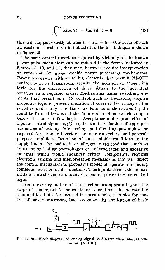
26 POWER PROCESSING
fJit
' [ak,e.*(t) - kreT(t)} dt = 0 (18)
this will happen exactly at time tk + Toli = tk^. One form of suchan electronic mechanism is indicated in the block diagram shownin figure 20.
The basic control functions required by virtually all the knownpower pulse modulators can be reduced to the forms indicated infigures 16, 18, and 19; they may, however, require interpretationor expansion for given specific power processing mechanisms.Power processors with switching elements that permit ON-OFFcontrol, such as transistors, require the addition of sequencinglogic for the distribution of drive signals to the individualswitches in a required order. Mechanisms using switching ele-ments that permit only ON control, such as thyristors, requireprotective logic to prevent initiation of current flow in any of theswitches under any conditions, as long as a short-circuit pathcould be formed because of the failure of another switch to openbefore the current flow begins. Acceptance and reproduction ofbipolar control signals er(t) require the introduction of appropri-ate means of sensing, interpreting, and directing power flow, asrequired for dc-to-ac inverters, ac-to-ac converters, and general-purpose amplifiers. Detection of unacceptable conditions in thesupply line or the load or internally.generated conditions, such astransient or lasting overvoltages or undervoltages and excessivecurrents, which would endanger critical components, requireselectronic sensing and interpretation mechanisms that will directthe control mechanism to protective modes of operation includingcomplete cessation of its functions. These protective systems mayinclude control over redundant sections of power flow or controllogic.
Even a cursory outline of these techniques appears beyond thescope of this report. Their existence is mentioned to indicate thekind and level of effort needed in operational electronics for con-trol of power processors. One recognizes the application of basic
s|
+ 1
— =H
H b̂R:
v
f0J &*k »ktl
FIGURE 20.—Block diagram of analog signal to discrete time interval con-verter (ASDIC).

ELECTRIC POWER TRANSFORMATION 27
techniques of electronic circuits used in analog and digital signalprocessing. The need for undelayed response to the continuedprogress of each cycle of the power system and the issuance of adhoc solutions on the duration of these cycles with accuracieswithin small fractions of 1 jusec imposes severe constraints on cir-cuit design. These constraints are further compounded by the factthat there is no room for even a temporary malfunction of theprotection system during any of the individual cycles of operationbecause such a malfunction could lead to the catastrophic failureof the power processor.
Other factors that contribute to the difficulties of design arethe absence of an external regulated source of electric energy topower the control system; the proximity of the power circuits ofthe pulse modulator to the associated sizable and abruptly chang-ing electromagnetic fields; and the disturbance of the primesource of electric energy by the pulsating mode of operation,often compounded by adverse environmental conditions. Furtherdifficulties are introduced by floating reference nodes of individ-ual control system parts that are associated with correspondingsections of the power system and the need for unerring communi-cation between these system parts that "ride" on different contin-uously or abruptly changing power waveforms. Positive signaltransfer, unaffected by relative reference node voltage variations,is needed under transient and static conditions of the system'scyclic operation. This type of operational requirement usually im-plies direct coupling and imposes the need for application of moresophisticated techniques, in contrast to capacitive coupling thatcan be freely applied in standard signal-level electronics.
Philosophy and techniques of operation of power processorshave been outlined in the preceding two sections. The rate of de-velopment of "both has been continually dominated by problems inthe areas of networks and components. These problem areas, andtheir effect on the efforts in the field of power processing, arepresented in the following section.

Problem Areas
CHARACTERIZATION OF PROBLEMS
The feasibility and reliability of static power processors dependlargely on the availability of semiconductor power componentswith characteristics that can satisfy the requirements of theirpower circuits. Instant or delayed catastrophic failure of thesecomponents can occur when component ratings, such as maximumvoltage, current, or allowable power dissipation, are exceeded foreven relatively short times. Thus, these semiconductor switchingcomponents must be selected to endure the largest expectedstresses due to applied potentials, currents, and heat dissipation.Estimates on the magnitudes of these stresses are based on in-tended steady-state operation with added allowances for irregularsource and load conditions and unintended cyclically recurringand transient voltage and current excursions including spikes.
Although the needed characteristics of switching elementsbased on the required power handling capability of the networkcan be readily calculated and established, no analytic methodshave been developed to calculate the other stresses that arecaused by dynamic system behavior and by the physical proper-ties and geometrical configuration of component materials. At-tempts to treat these areas quasi-analytically appear restricted toapplication of iterative computerized numerical analysis, referredto as network simulation or computer-aided circuit design. Theseapproaches will permit, at best, the acceleration of trial-and-errorprocesses but are burdened with the inherent limitations of in-complete device modeling. As a result, the designer finds himselfin the position of having to derate the switching components sub-stantially to allow for contingencies whose existence is known butwhose magnitudes are rarely known. Derating is roughly propor-tional to the degree of reliability of operation and can reduce thepower handling capacity of a power transistor by an order ofmagnitude when ultrareliability is required, as with power con-version equipment on a manned spacecraft.
Even then the designer does not know what margin of safety,if any, is left or whether his design is inherently unreliable. He
29

30 POWER PROCESSING
needs information on the interdependence of the nonlinear char-acteristics of components interacting in circuits that function innonlinear modes, such as those that implement pulse modulationprocesses. His task is compounded by the fact that satisfactoryanalysis of these networks would still be cumbersome, even if thisinterdependence of component characteristics were better under-stood—there are no established and practical methods of analysis.
SWITCH-INDUCTOR-TRANSFORMER INTERACTION
One of the classic problems encountered in power pulse modula-tion is that of interruption of current in an inductor. In fact, flowof current in an inductor cannot be abruptly terminated, and theattempt to do so will lead to a breakdown of other componentsunless another path of current flow is provided.
Virtually all pulse-modulated power processors incorporate in-ductive elements in their circuits that can be either intended orparasitic, unlike their signal-level electronic counterparts. Whenthe current is interrupted in the course of transferring the storedmagnetic energy to either the load or capacitive elements, a frac-tion of this energy is dissipated in the parasitic resistive elementsof the circuit. The distribution of the resulting conversion of themagnetic energy to heat in the circuit is proportional to the rela-tive magnitude of the resistive elements within this circuit. Thelargest of these resistive elements is invariably the switch in theprocess of opening. This discharge of magnetic energy manifestsitself in the form of voltage and current spikes that appear at thetermination of individual cycles of power pulse modulators. Manydesigners of power processing equipment are well aware of thesephenomena, which are usually but not always due to parasitic ef-fects associated with power components and networks.
The parallel inverter, illustrated in figure 10, incorporates atleast two functions that can be cited as examples. The currentsflowing alternately through the primary inverter circuits are ter-minated by opening of switches CSSj. These switches, in effect,interrupt the current flowing in filter inductor LF. The problem,then, is the transfer of the current from switch S2j to SF concur-rent with the interruption of the same current by the controlledsampling switch CSSi. The diagram of the network under consid-eration should be modified to replace the simple switch symbolsby their more representative equivalent circuits, and to includethe secondary characteristics of the inductor to permit a detailedtransient analysis of this process under the given "large signal"conditions. To understand the processes involved and to design an

PROBLEM AREAS 31
optimum system, the nonlinear characteristics of the elements in-volved during their respective transitions through delay, rise,storage, and fall times require careful modeling and close under-standing and correlation of the nature of these modeling proc-esses with each other during all phases. This study should clarifythe phenomena associated with these transitions, including thewaveforms of voltage and currents at the component terminals,and the time and spatial distribution of these potentials, currents,and resulting heat dissipation within the switches. This informa-tion would provide a significant contribution to the understandingof stress mechanisms and permit judicious application of designcriteria. No successful analysis of this type has been reported.
The real characteristics of the power transformer X of the par-allel inverter have not been considered up to this point. This ap-parently simple device assumes considerable complexity duringabrupt current flow transitions within time intervals on the orderof microseconds (ref. 7). The simple transformer symbol infigure 10 is replaced by an equivalent circuit to fit the conditionsduring abrupt transitions and other conditions. These equivalentcircuits include lumped parameters to approximate the effects ofdistributed and time-varying electromagnetic fields that are dueto interwinding and intrawinding capacitances, leakage induct-ance, apparent power losses in ferromagnetic core materials, skineffects, and induced eddy currents in conductors, to name somesignificant phenomena. The analysis of even the simplest inverternetwork containing all the significant parameters of semiconduc-tor and electromagnetic wirewound components is very complex.The interaction between the transistor switch in the primary cir-cuit of a parallel inverter and the magnetic energies stored in theleakage inductance and the airgap of the magnetic core of apower transformer is briefly considered as an example for suchan analysis.
The forcible interruption of current flow at the termination ofeach pulse is initiated by application of a turnoff signal to thebase terminal of transistor CSSj. The actual opening process isinitiated after the transistor's storage time has elapsed. The mag-netic energy stored in the leakage inductance of the primary cir-cuit and in the airgap of the transformer is unable to return tothe network inconspicuously, as it does under conditions of sinus-oidal excitation. The stored magnetic energy will attempt to ad-just the potentials of transformer terminals so that this energycan be transferred to the associated circuits. This process neces-sarily leads to dissipative conversion of electromagnetic energy toheat at times when this energy is not transferred to other energy

32 POWER PROCESSING
storage elements for potential reuse. The return of the magneticenergy to the primary inverter circuit manifests itself by the oc-currence of voltage and current spikes at the trailing edges ofeach individual pulse appearing across the terminals of switchesCSSi (fig. 21). These spikes interact with the opening process ofthe switch and modify substantially the switch component charac-teristics that otherwise appear within resistance-capacitance(RC) networks in which the characteristics are usually estab-lished. It is expected that a reduction of these spikes will alleviatethe stresses on the switching component.
One way to reduce these sudden waveform excursions is to re-duce the amount of returnable energy stored in the magneticfields of the transformer. Such a reduction could be accomplishedby the complete elimination of the airgap of the transformer coreand the use of ferromagnetic core materials that are character-ized by "square" and narrow BH loops. Use of such cores elimi-nates the airgap problem and reduces the leakage inductance oftransformers considerably. It introduces, however, the problem ofsaturation currents due to the absence of the airgap that other-wise centers the BH loop around the origin of the BH coordi-nates. This problem is compounded by the delay interval Td be-tween the instant of detection of transformer core saturation attime Tf and the actual completion of the opening process ofswitch CSSi at time Tk. The typical magnetizing current im ofthe transformer normalized with respect to its nonsaturated aver-age magnitude imn is depicted in figure 22. Operation of invert-ers involving these current waveforms was first introduced byRoyer (ref. 8) and later modified by Jensen (ref. 9).
The interaction between the parasitic effects in high-frequency
c— T,
(0) (b)
FIGURE 21.—Waveforms at switches CSSi of parallel inverters: (a) voltageand (b) current.

PROBLEM AREAS 33
power transformers and the physical shortcomings of semicon-ductor switches constitutes one of the most serious problems inpresent power processing systems. The delay Td in opening switchCSSj causes an increase of the magnetizing current toward i™ (7\),a multiple of the load current iL even though the ratio of the "non-saturated" magnetizing current to the intended load current imn/iz,«l by virtue of required transformer efficiency. The increasedprimary current in(Tk) — im(Tj,) + itj then increases from its"normal" value ilin = iL to a multiple km»l such that z'ii(Tfc) =fcmt'ii,, as indicated in figure 21. The energy stored in the leakageinductance at time Tk is then increased by the factor km
2 from itsformer value when ilin = iL provided sufficient base drive is ap-plied. The switch opening process is thus further complicated.
This problem has been attacked in two ways. The first attemptwas to devise and implement a pulse modulation philosophy thatcompensates for the modulation error caused by the turnoff delayTd by adjustment of the aperiodic cycle duration Tom =£ Ton; thesecond was to center the BH loop of saturable core transformersaround the coordinate origin. The required type of modulation isprovided by control mechanisms discussed with reference to fig-ures 18 to 20. The significance of the last statement is explainedby reference to the illustration of a flattop pulse in figure 23.
The discrepancy between the preprogramed (shaded) rectangu-
FIGURE 22.—Waveform of normalized magnetizingcurrent im/imn in free-running parallel inverterwith saturable core transformer.
FIGURE 23.—Preprogramed and ac-tual single flattop power pulse.

34 POWER PROCESSING
lar pulse with duration TP and the actual pulse as "seen" by thecontrol network is self-explanatory. The functional error that thisdiscrepancy introduces into the control mechanism is removed byappropriate adjustment of the cycle interval Tok to the actualtime integral of the kih pulse as expressed by relations (14),(16), and (17) (ref. 2, chs. II and III). This type of control em-ploys mixed PWM-PFM control because only a subsequent adjust-ment of interval Tok can satisfy relation (17) if there is no wayto control the pulse area integral accurately, and PWM with afixed period for intervals T0 = Tok lacks the required degree offreedom. For these reasons use of mixed PWM-PFM eliminatesthe need to develop transistors with shorter storage times Td.
The problem of transformer saturation during switch openingas illustrated in figure 22 has satisfactory solutions (ref. 10). Os-cilloscope traces of the current waveforms in the primary circuitsof a free-running pulse-modulated parallel inverter before andafter application of a new technique are presented in fig_ure 24.
(0)
VERTICAL:1. 5 A/cm2. 20 V/cm
HORIZONTAL: 50 /isec/cm
(b)
VERTICAL:I. 5 A/cm2 20 V/cm
HORIZONTAL: 50 /isec/cm
(c)
VERTICAL:1. 10 V/cm2. 2 A/cm
HORIZONTAL: 0.5 /isec/cm
MlVERTICAL:
1. 10 V/cm2. 2 A/cm
HORIZONTAL: 0.5 ^s
FIGURE 24.—Current and voltage waveforms in primary circuits of free-running inverters, (a) Drive signal removed after initiation of trans-former core saturation. (6) Transformer with centered BH loop, (c) Lead-ing edge of current waveform, (d) Trailing edge of current waveform.

PROBLEM AREAS 35
The significance of this technique consists in the fact that thecurrent spikes illustrated in figure 24 (a) are not suppressed butprevented. The heating effects within the power transistors thatare due to this phenomenon are completely eliminated, a signifi-cant fact because the localized stresses due to high, fast changingcurrent densities within the transistor constitute a considerablereliability hazard.
As a consequence of this improvement, it can be expected thatderating of power transistors could be substantially reduced. Theload current carrying capacity of the available switching ele-ments could be increased accordingly to a multiple of its presentmagnitude. This reduction of the need for derating of switchingcomponents should permit design of parallel inverters with sub-stantially higher power capacities than.is presently possible.
The series capacitor inverter indicated in figure 13 eliminatesunfavorable effects of interaction between transformer andswitching elements to a large extent. The current waveform ofthe individual pulses is that of half sinusoids, which are termi-nated by turnoff of the silicon-controlled rectifier when the cur-rent falls to zero. The current waveform within such inverters isindicated in figure 25. Energy stored in the magnetic fields associ-ated with the pulse currents is transferred to the series capacitorbefore opening switch CSS, because of cessation of current flow.Using this type of operation, the switches can be closed andopened with essentially no current flow and freedom from theharmful effects of discharge of magnetic energies during theswitch opening process. The series capacitor inverter requirescareful design of the electronic control mechanism and an under-standing of the physical limitations of the controlled rectifiers be-cause inadequacy of design could lead to immediate failure; incomparison, the parallel inverter may suffer from an initial re-duction of efficiency and eventual failure under similar condi-
FIGURE 25.—Wave of current isi* with res-onant turnoff in series capacitor inverter.

36 POWER PROCESSING
tions. The inadequacies of series inverters were caused by the ne-cessity to overdesign transformers and inductors substantially s6that the associated converter systems could cover a wide range ofloading. Recent advances removed this difficulty and led to suc-cessful implementation of a 2-kW converter (ref. 11).
ELECTRONIC SWITCHING ELEMENTS
The displacement of rotating inverters and converters by staticelectric power inversion and conversion equipment was initiatedwith the advent of electron tubes during the first decades of thiscentury. Moderate efficiency and reliability restricted the use ofstatic inverters to specialized applications, such as induction heat-ing, that could tolerate the associated elevated cost. Frequency ofoperation was limited to approximately 1 kHz because of the rela-tively long deionization time in mercury vapor electron tubes. Re-cent advances in electron-tube technology and the use of gasessuch as xenon with considerably shortened deionization times per-mit operation at frequencies of several kilohertz. However, therelatively large forward voltage drop in these tubes, the neededfilament heating power, and the fragility of mechanical struc-tures, including that of the filament itself, severely restrict theuse of these tubes. The power semiconductor components havecontinued to displace both rotating and static electron-tube powerconversion equipment because of the relatively high efficiency andreliability of these components.
Essentially, the power transistor differs from its signal-levelcounterpart by the size it requires to carry relatively large cur-rents. The associated larger geometries inherently offset improve-ments in transistor characteristics, such as fast delay, rise, stor-age, and fall times, desirable for more accurate pulse control athigher frequencies of operation; better compatibility with trans-formers and inductors; and minimization of energy dissipation atthe fringes of pulses. The relatively thin, fragile base remains amatter of concern because it is believed to be the site of mostpower transistor failures under conditions of excessive stresses.These stresses lead to localized excessive potential differences oroverheating due to temporary concentration of currents.
One way to provide ample current carrying capacities and (yetpreserve the favorable characteristics of smaller transistors is toput a number of smaller transistors in parallel and enclose themin a common package. The obvious problem associated with thistechnique is that of load sharing. Conscientious selection andmatching of individual transistors tends to reduce this problem.

PROBLEM AREAS 37
This solution, however, leaves doubts about the preservation ofthe match of characteristics throughout the process of aging andintroduces an added reliability hazard. The characteristics andproblems of transistors are well covered in the pertinent litera-ture. The purpose of this discussion, therefore, is to emphasize theneed for useful information on the characteristics of power tran-sistors to the designer of power processing equipment.
Information contained in the specifications of power transistorsusually describes this device in terms of characteristics neededfor signal-level operation in the linear region of operation. Infor-mation of vital significance about component characteristics inthe intended ON-OFF switching modes of operation such asdelay, rise, storage, and fall times and their dependence on oper-ating conditions is scant, if provided at all. The data that charac-terize these components are often obtained under unrealistic testconditions, such as purely resistive circuits or, at best, RC cir-cuits. The information contained in the specifications does providea general orientation on the applicability of the device under con-sideration. The power transistor, however, is almost exclusivelyused in networks that include inductors and transformers withsignificant inductive characteristics. The designer circumventsthe difficulty that results from a lack of knowledge of componentbehavior by derating these switching devices considerably. But hedoes not know how effective this derating process actually is andhas to rely on his experience, intuition, and the outcome of exten-sive testing of power conversion systems as closed entities.
A better understanding of the interdependence between charac-teristics of semiconductors and electromagnetic devices such as in-ductors and transformers seems necessary to provide guidance forthe improvement of power semiconductor components capable offunctioning in a manner that will fulfill the requirements of solid-state power processing apparatus. Continued efforts for reduc-tion of turnoff times of power transistors below 1 jusec should beviewed critically because the speed of the turnoff process may belimited by the time constants of the associated electromagneticcomponents rather than by the electronic switch. These time con-stants can be considerably larger than the achievable transistorturnoff times and would curtail the usefulness of the fruits ofsuch tedious and expensive efforts.
The silicon-controlled rectifier tolerates relatively irregular op-erating conditions, such as considerable transient excess stressdue to applied potentials or carried currents, and is the most im-portant switching element for high-power static conversion equip-

38 POWER PROCESSING
ment. Its availability with substantial ratings such as breakovervoltages on the order of kilovolts and current carrying capacitiesof several hundred amperes in single units seems to designatethis p-n-p-n-type switching element as the workhorse of powerprocessing equipment. This switching element indeed finds appli-cation in virtually all power conversion systems that require a ca-pacity greater than i/fc to 1 kW for single units. Its application is,however, largely restricted to systems that are being operatedfrom ac sources.
The overriding reason for this restriction is the lack of controlover this switch after current flow has been initiated. Alternating-current operation would necessarily lead to the reversal of cur-rent flow and thus open the switch. In a de-powered system thisis, of course, not true. A number of techniques have been devel-oped to implement turnoff mechanisms for this device. Turnoffcircuits that are externally associated with the controlled recti-fiers and built-in mechanisms that permit gate turnoff by removalof the carriers from the junction below the required minimumconcentration for conduction are commonly used for this purpose.This type of controlled rectifier operation has found wide applica-tion in terrestrial and marine technology where incidental failureof one turnoff process can be remedied by replacement of a fuse.Designers, however, are reluctant to use this switch in applica-tions where continued and uninterrupted operation is vital, suchas in aircraft and spacecraft. An exception is the series inverterthat positions a series capacitor between the dc source power lineand its reference node at any time. However, more work isneeded in this area before these systems could become opera-tional.
The controlled rectifier restricts the frequency of operation ofpower processing equipment to approximately 10 kHz because itneeds a recovery time of approximately 10 /xsec. At 10 kHz, thisresults in a maximum duty cycle Tk/Tok of 0.8. Reduction of therecovery or turnoff time will permit an increase of operating fre-quency. It should be possible to reduce this turnoff time to theorder of 1 ;u,sec by construction of interdigitated gates and by ap-plication of ion implantation techniques. This should permit oper-ating frequencies on the order of 100 kHz and reduction of thephysical weight and size of multikilowatt dc-to-dc converters toless than 1 Ib/kW while maintaining efficiencies well in excess of90 percent.
It can be said that the transistor constitutes the presently pre-ferred switching element for power converters with capacities up

PROBLEM AREAS 39
to several hundred watts per single unit. Its application is re-stricted to relatively low input voltage consistent with the rela-tively low power application. Typical voltages are 28, 36, and, attimes, 56 or 80 V. The silicon-controlled rectifier can handlepower levels up to approximately 100 kV-A when applied in pairsto single converter units. Its application to de-driven systems thatrequire a high degree of reliability is subject to successful demon-stration of newer techniques. Experimentally acquired data onthe efficiency of this type of converter (ref. 11) are indicated infigure 26.
TRANSFORMERS AND INDUCTORS
Transformers and inductors are the key elements in powerprocessing systems. The transformer has the ability to scale po-tentials and to provide reference node isolation. The inductor is anecessary requisite for all electronic power mechanisms that op-erate in a pulsating mode. It is the component that will bridgethe abrupt and time-varying discontinuity of potentials of adjoin-ing components inside the conversion mechanism and provide thelink for power transfer under these conditions.
The technology of transformers and inductors, as currentlyknown, dates back to the decades before the turn of the century.
SERIES CAPACITOR DC TRANSFORMER EFFICIENCY AS FUNCTIONS OF OUTPUT POWER WITHINPUT VOLTAGE AND INPUT CURRENT AS PARAMETERS
oC .90
OUTPUT, kW
FIGURE 26.—Series capacitor dc transformer efficiency as functions of outputpower with input voltage and input current as parameters.

40 POWER PROCESSING
Their design and construction have remained almost unalteredexcept for improvement of materials. The currently appliedarchaic design methods consist of tedious trial-and-error proce-dures in which the designer selects magnetic cores by experienceand intuition, goes through a number of paper designs in succes-sion, compares them with each other in reference to physicalweight, size, efficiency, and cost, and finally selects the one withthe most favorable characteristics. Mechanization of these trial-and-error methods by use of digital computers provides some re-lief. However, the development of comprehensive modularizedprograms is needed so that the multitude of parameters associ-ated with materials properties, geometric core configurations, andapplied waveforms, beyond reported attempts in this field, can beincluded (refs. 12 and 13). The designer can choose among a rela-tively large variety of magnetic materials with various perform-ance characteristics available in many geometrical configurations(refs. 14 and 15). He can also choose among various types of coreconstruction, such as a sintered ferrite core or a magnetic coreformed from wound thin tape or a stack of laminations, againwith a choice of various thicknesses of tape or lamination (ref.16). The area of standard power transformers for 60-Hz, and tosome extent for 400-Hz, operation under conditions of sinusoidalexcitation has been relatively well covered over many years. Thedesigner of the transformers and inductors for power processingequipment that usually operates at substantially higher internalfrequencies finds himself faced with the task of designing compo-nents solely from his knowledge of electromagnetics, including fer-romagnetics, for conditions of operation, including voltage wave-forms and frequencies, not previously encountered or described intextbooks. Moreover, important material properties like the appar-ent core loss in magnetic material under conditions of nonsinusoidalexcitation are not recorded. Nor, except for very isolated cases(ref. 17), is there a known method to apply the information oncore losses under known conditions, such as sinusoidal excitation,to the nonorthodox waveforms that are encountered in powerprocessing systems. This lack of information about how to copewith problems like the magnetic core loss effects due" to rectangu-lar voltage waveforms with varying duty cycles having triangularor quasi-sinusoidal waveforms, as encountered in certain types ofinverters, forces the designer to attempt to substitute heuristicassumptions for the lack of needed knowledge.
The transformer designer is faced with a similar problem if hetries to evaluate the significance of parasitic effects in wire-

PROBLEM AREAS 41
wound magnetic components in detail. The significance of theseeffects and their interaction with the nonlinear characteristics ofsemiconductor components have been discussed. An impressivemultitude of publications exists in the area of transformer de-sign. A closer examination of this literature reveals that they areconcerned with the low- or high-frequency transformer underconditions of sinusoidal excitation or with the wideband or pulsetransformer used for specialized application, but not with thepower transformer in abruptly switching networks (refs. 18, 19,and 20). It is not unusual for a transformer designer to attemptto place his transformer into a circuit environment that is knownto hini by experience rather than to venture into an area of inno-vation. This appears to be true even if that experience conveys tothe designer more of a familiar environment than actual knowl-edge. Besides the lack of essential knowledge, the quest for lowerweights and higher efficiencies, and thus higher frequencies of op-eration, counteracts the possibility of using reflective design pro-cedures and constitutes one of the significant causes of difficultyin this area.
Another problem area is that of transfer of heat generatedwithin the electromagnetic devices. The same amount of heat isgenerated within the smaller geometrical volume of a trans-former when its physical size is reduced at higher frequencies ofoperation and its efficiency remains unaltered. One of the possiblesolutions to this problem appears to be a further improvement ofthe efficiencies of transformers by\ more extensive application ofhigh-efficiency magnetic materials with narrow BH loops. This inturn requires a better understanding of the involved phenomenaand material properties, reinforced by deterministic methods ofanalysis and synthesis of design.
CAPACITORS
The reliability and stability of dc filter capacitors cause con-cern in the area of power processing. Electrolytic capacitors packedto high energy densities employ relatively thin electrodes, whichconstitute one of the causes of insufficient reliability. The succes-sive interchanges of metal between the electrodes and the electro-lyte are not necessarily uniformly distributed over the area of in-teraction. This can lead to the appearance of holes in theelectrodes that will eventually enlarge because of the associatedfield effects. Furthermore, these capacitors suffer from a lack ofstability of their capacitance value as a function of temperature.Variation of capacitance in dc filters affects the attenuation capa-

42 POWER PROCESSING
bility of these filters, which produces a variation of ripple volt-ages. Appropriate overdesign can be applied to limit these ef-fects. However, the effects of varying capacitance on the stabilityof feedback systems such as power processors are cumbersome todeal with and often require the application of tedious compensa-tion techniques that may vary from unit to unit and with age.The use of all kinds of electrolytic capacitors, including those thatcontain tantalum materials, has been excluded from certain areasof technology such as manned space flight because their short-comings could have critical effects. However, even in these areasthe lack of other capacitors with comparable energy densityforces engineers to use these components and to accept the prob-lems associated with their use, one of which is the adverse effectson reliability and stability of the power processors. Thin-filmmetal oxide capacitors with energy densities that equal or per-haps exceed those of electrolytic capacitors are expected to im-prove this situation. Excellent temperature stability and high en-ergy density have been demonstrated by these capacitors. Theiruses, however, are only now being explored. (See fig. 27.)
The reason that conventional metal film capacitors have not
EFFECT OF TEMPERATURE ON CAPACITANCE VERSUS FREQUENCYRELATIONSHIP FOR AI-Si02 MULTILAYER CAPACITORS
0.0114
0.0113
J 0.01 12•
>
: o.oi ii
O.OIIO
0.01 09
0.01081
\\ T=3I4°C
\
\
T=I34'C ••T=22°C
V
\v\\
^^•^•^— ̂ .̂̂ ^« ̂ ^^^^_
W9"C
v\
- — -^
O1 I02 I03 10* I05
FREQUENCY, Hz
FIGURE 27.—Effect of temperature on capacitance versus frequency relation-ship for A1-S1O2 multilayer capacitors.

PROBLEM AREAS 43
been greatly used for ac circuits within power processors is thelack of sufficient information on the suitability of currently avail-able capacitors for this. The designer has to turn to specializedmanufacturers who can provide him with custom-made compo-nents. This process requires the designer to be familiar with ca-pacitor characteristics, properties, and often the feasibility ofmanufacture. The designer often decides against such a tediousand costly procedure and uses inadequate components designedfor signal-level use instead.
Analysis of power networks which include components withnonlinear characteristics calls for a wattmeter with a bandwidthfrom dc to approximately 1 MHz to indicate the nature of dissi-pative processes within these components associated with ab-ruptly changing voltage and current waveforms. Currently avail-able wattmeters are restricted to frequencies of several kHz atspecific power factors and, therefore, are not suited for this pur-pose. An experimental instrument that, in addition to the com-mon scale indicator, displays the power dissipation within a cer-tain component as a function of time on a conventionaloscilloscope is presently under development (ref. 21). Collectorvoltage and the corresponding power dissipation in a p-n-p tran-sistor are illustrated in figure 28.
STABILITY
Stability analysis of power processing apparatus is often re-stricted to iterative experimental observations and adjustments tothe design near the completion of a development program. Appli-cation of damping methods usually leads to a condition that isconsidered satisfactory although it deprives the system of theneeded capability to react against disturbances that appear on thesupply line and the effects of sudden load changes or other dis-
FIGURE 28.— (a) Collector voltage and (6) relative power dissipation oftransistor 2N1184A with 2-A collector current. Collector voltage is 5 V/cm,input pulse is 25 usec, and base drive is 2, 5, 10, and 20.

44 POWER PROCESSING
turbances that may enter the system. At times, attempts aremade to apply the methods of linear feedback analysis to powerprocessors. Unfortunately, the simple and powerful methods oflinear control system analysis are not appropriate for networksof power processors, primarily because these methods were devel-oped for systems whose characteristic equations contain realroots that arise from time constants associated with RC and re-sistance-inductance (RL) combinations within the networks.However, power processing systems include numerous compo-nents having nonlinear characteristics near their regions of tran-sition from one state to another. Outside these regions, one couldthink of these systems as being piecewise linear; however, apiecewise linear system is nonlinear by definition and, therefore,cannot be analyzed by linear methods. This property is under-lined by the inherent limitation of a power processor to certainlevels of potentials in its input or output stages. The limitation ofthe power amplifier by its saturation levels is another significantnonlinear characteristic that becomes apparent under conditionsof dynamic operation such as turn-on of the power system, abruptload changes, and other transient disturbances that the powercontrol system should react to and stabilize. A search of the litera-ture for methods of analysis of the aperiodic or nonuniformaperiodic sample data systems soon reveals that no useful methodexists that indicates under what specific conditions and by whatmargin these feedback systems will be stable. Thus, technical in-formation is sorely needed on the dynamic behavior of these feed-back systems under steady-state and transient conditions. Thesolutions to these problems are not simple. When formulated, theylead to differential equations with time-varying coefficients. Tocomplicate matters, the variation of each of these coefficients isdetermined by the outcome of previous operations.
Intensive work is needed in the field of stability analysis to es-tablish, an8 provide the designer of power processing apparatuswith, the tools needed to ascertain a priori whether a stable sys-tem can be realized for certain given conditions. The importanceof this work becomes obvious when we realize that it shouldgreatly improve .the reliability of the systems and reduce thenumber of trial-and-error methods currently in use.
A digital computer was used in an attempt to provide the kindof information needed to analyze the stability of a system undergiven conditions of operation. A power pulse modulator was mod-eled on a digital computer after its significant parameters werenormalized. Data concerning the response to unit step inputs

PROBLEM AREAS 45
under practical conditions were obtained and organized to allowthe designer to anticipate the degree of stability of the systemunder given conditions of operation. Figure 29 is the kind of
AVERAGE SAMPLING RaTENATURAL OUTPUT FILTER FREQUENCY
ooooooooooooooooooooooooo
LEGENO OF OUTPUT VOLTAGE CHARACTERISTICS
• NORMALIZED STEAOr STATE OSCILLATIONSOVERSHOOT IN PERCENT
OOOOOO RISE TIME IN OUTPUT FILTER TIME CONSTANTSa-A-a-A SETTLING TIME TO LESS THAN ±0.5 PERCENT DEVIATION
SETTLING TIME TO LESS THAN ±0.1 PERCENT DEVIATION
1 1 I I
2.0 8.0 32.0
AIE5.0 250.0 500.O lOO'O.O
FIGURE 29.—Response of pulse modulator illustrated in figure 9 to unit stepinput.

46 POWER PROCESSING
graph that can be obtained by this procedure and contains infor-mation, for the pulse modulator being considered, on (1) steady-state oscillations; (2) rise time, overshoot, and settling time asfunctions of the feedback gain; and (3) the damping ratio | of anL-type inductance-capacitance (LC) filter; and (4) the ratio v ofaverage pulse repetition rate to the natural frequency of thatfilter. Integration of the use of graphs like these into the designprocess should permit the designer to establish beforehand thestability of his pulse-modulated dc-to-dc converter. A design proc-ess based on the significant results of computer modeling shouldprovide detailed information on the significant dynamic proper-ties of these converters and could be part of a deterministic com-puterized synthesis method rather than to resort to customarymethods of computerized network simulation.
EDUCATION AND TRAINING OF PERSONNEL
Engineers in the field of electric power processing come fromvarious areas of electrical engineering. One relatively small groupis that of classical electrical power engineers who, at some timein their careers, needed to apply modern static power conversionto the programs within their areas of responsibility. Anothersmaller group from the area of magnetic amplifiers found betterways to implement the nonlinear philosophies of operation ofmagnetic amplifiers by way of faster and more flexible semi-conductor components. Another small group was supplied by thediscipline of control systems engineering. The largest group,however, is from the area of electronic circuit design.
Many electronic circuit designers are at one time or anotherexposed to the need to stabilize power for sensitive networks.Electronic power networks differ from their signal-level counter-parts in the size of voltages, currents, and power dissipation intheir individual components. The philosophy of operation ofpower pulse modulators is closely related to that for pulse modu-lation in the area of communications technology. The significantdifficulties that arise for the electronic circuit designer when en-tering the field of power processing are rooted in the requirementfor efficient operation of power networks. The variable resistivecomponent, the transistor that implements the wave-shapingprocess, is eliminated. Further, inductors and transformers areintroduced for operation at relatively high frequencies; thesecomponents are rarely used in conventional signal-level electron-ics. The networks under consideration consist of inductive, capac-itive, and ON-OFF switching elements. No didactic literature

PROBLEM AREAS 47
appears available that concerns itself with the quantitative treat-ment of lossless voltage waveform transformation at power levelsand its implementation by nonlinear LC networks under condi-tions of abrupt switch modulation. The same holds true for text-books or other teaching material on the stability of pulse-modu-lated LC feedback networks.
The requirements for competence of electrical engineers in thisfield are rigorous. They should have a working knowledge of thetheory and design of nonlinear active filters that eliminate resis-tive components for any functional purpose and an ability to ana-lyze these systems under open- and closed-loop operation. Thesetwo requirements are imposed by the necessity of producingequipment that will operate without fail. However, no coursework concerned with practical attainment of these objectivesseems available at any university.
A thorough study of system and control theory to acquire aworking knowledge of the advanced tools of mathematics for theanalysis of time-varying systems should form a point of depar-ture into the unknown and problematic areas associated withpower processing technology. Beyond this, the engineer has torely on his intuition, which is based on his general training andrelated experience, to produce working equipment.. He must alsobe able to design pulse, digital, and switching circuits under theaggravating conditions of operation from unstabilized sources.These circuits have reference nodes, whose potentials vary withrespect to each other, yet require positive and unfailing transmis-sion of intelligence within the circuits and over the boundaries ofthe time-varying reference node potentials. The circuits operate,furthermore, near sizable electromagnetic fields that are causedby the abrupt switching of power networks. In addition, theyoften must operate under adverse environmental conditions. Theneeded reliability of this circuitry requires positive relation ofeach function to the past history of the power network and its as-sociated electronic logic in order to assure reliable continuation ofoperation under conditions of transient disturbance. This elimi-nates the use of any capacitive coupling between networks andrequires the application of complex techniques for the'transmis-sion of signals over the barrier of time-varying node potentials.In the area of control electronics, the engineer can expand on hisbasic education. Nevertheless, extensive training in the generalphilosophy and physical implementation of analog and digitallogic is required in addition to the knowledge that is contained inrepresentative textbooks (ref. 22).

48 POWER PROCESSING
The classical power engineer seems to be more knowledgeableabout power components, especially transformers and inductors,than his electronic colleague. Training in this area, however, isunfortunately almost exclusively restricted to utility power appli-cations, a firmly established technology that has remained rela-tively static for decades. The result is that a study in depth of theelectromagnetic processes, and the associated ferromagnetic phe-nomena, is not a part of the training of engineering students. Thepower engineer often lacks needed training in the advancedmethods of applied mathematics. Often in engineering curricula,more time is devoted to utility power technology than to thebroad principles of electrical engineering. The study of trans-formers, therefore, is often limited to the methods of frequencydomain analysis of utility power transformers than to an under-standing of the transformer in a broader sense. The power proc-essing engineer requires an understanding of transformers thatis based on a quantitative description of phenomena in the timedomain because the waveforms and the modes of operation thathe encounters are described in this domain. In the analysis oftransformers, applying Fourier series expansions of abruptlychanging waveforms is extremely cumbersome and obscures anunderstanding and insight into the quantitative relationships be-tween the significant phenomena. Thus, both the power engineerand the electronic engineer are not trained well enough whenthey enter, from different directions, into the field of power proc-essing.
This field suffers from the lack of younger talents who are suf-ficiently interested and capable to make it their profession. A sig-nificant impediment for entrance into this field is the lack ofunderstanding of what it is and the belief that anything associ-ated with the notion of electrical power engineering is unchal-lenging and, worse yet, unglamorous. The requirements for theabilities of an engineer in this field, as developed throughout thisreport, are severe and require many years of intensive study andtraining at an unusually high level of sophistication. The encour-agement of students to work toward such a goal will have tocome from the faculty members of our universities. This, in turn,requires that the problems of this area be brought to the atten-tion of our teachers of electrical engineering to acquaint themwith the sophistication and the challenge contained in theseproblems.

Summary
Processing of electric power has been presented throughoutthis report as a discipline that draws on almost every field ofelectrical engineering, including system and control theory, com-munications theory, electronic network design, and power compo-nent technology.
The cost of power processing equipment, which often equalsthat of expensive, sophisticated, and unconventional sources ofelectrical energy, such as solar batteries, is a significant considera-tion in the choice of electric power systems. Its reliability appearsin urgent need of improvements since it is believed that the over-whelming majority of failures in sophisticated electric systemsoriginate in the area of power processing. There exists a miscon-ception that this field, which is at this time just emerging in thewake of solid-state components, is well established. This miscon-ception seems to be the cause of the insufficient concern with thisfield seen in educational institutions and all ranks of engineeringmanagement. The valuable work accomplished in the last decadeis due to successful attempts by individuals from other areas ofelectrical engineering to interpret the problems in the light oftheir abilities and to educate themselves to meet the challenge ofthese problems. To achieve this, power engineers have venturedinto this area and tried to understand and utilize the characteris-tics of semiconductor components, whereas electronic engineershave tried to apply and modify the theory of signal-level elec-tronic networks.
Every power converter developed today is a piece of art, cre-ated by a group of capable individuals, which cannot be modifiedbecause of a lack of understanding of the principles involved andtheir quantitative interpretation. Other areas of technology, forexample, communications and control systems, underwent a simi-lar pattern of -development in a not too distant past, when, afterinitial establishment as useful technology, they were permeatedwith the rigorous methods of mathematical analysis and thustransformed from an art to a science.
49

References
1. SHANNON, C. E.; AND WEAVER, W.: The Mathematical Theory of Com-munication. Univ. of Illinois Press, Urbana, 111., 1949.
2. SCHWARZ, FRANCISC C.: A Class of Nonlinear Active Filters With Ap-plication to Electric Energy Conversion. Ph. D. thesis, Cornell Univ.,1965.
3. SCHWARZ, FRANCISC C.: Frequency Modulated Self Stabilizing Inverter.U.S. Patent 3,303,405, 1967, filed 1963.
4. D'Azzo, J. J.; AND HOUPIS, C. H.: Feedback Control System Analysis andSynthesis. McGraw-Hill Book Co., Inc., 1966.
5. SCHWARZ, FRANCISC C.: Switch Modulation Techniques, Parts I and II.Proceedings of the 16th and 17th Power Sources Conferences, 1962and 1963.
6. SCHWARZ, FRANCISC C.: Self Stabilizing Pulse Duration ModulationAmplifier. U.S. Patent 3,311,808, 1967, filed 1962.
7. GLASOE, G. N.; AND LEBACQZ, J. V.: Pulse Generators. MIT RadiationLaboratory Series. McGraw-Hill Book Co., Inc., 1948.
8. ROYER, G. H.: A Switching Transistor DC to AC Converter. Trans.AIEE, vol. 74, pt. 1, July 1955, pp. 322-324.
9. JENSEN, J. L.: An Improved Square Wave Oscillator Circuit. IRE Trans.Circuit Theory, vol. 4, no. 3, Sept. 1957, pp. 276-279.
10. SCHWARZ, FRANCISC C.: An Unorthodox Transformer for Free RunningParallel Inverters. IEEE Trans. Magnetics, vol. MAG-5, Dec. 1969,pp. 908-912.
11. SCHWARZ, FRANCISC C.: A Method of Resonant Current Pulse Modulationfor Power Converters. IEEE Trans. Industrial Electronics and Con-trol Instrumentation, vol. IECI-17, no. 3, May 1970, pp. 209-221.
12. WILDFEUER, D.: The Use of Automatic Digital Computation Machine inDesign of Miniature Pulse Transformers and Power Transformers.Proc. Natl. Electron. Conf., vol. 16, 1960, pp. 631-651.
13. JACKSON, S. P.: Optimization of Transformer Geometry by Method ofFinite Increments. AIEE Preprint 61-789, New York, 1960.
14. BOZORTH, R. M.: Ferromagnetism, van Nostrand, New York, 1951.15. STORM, H. F.: Magnetic Amplifiers. John Wiley & Sons, Inc., 1955.16. GROSSNER, N. R.: Transformers for Electronic Circuits. McGraw-Hill
Book Co., Inc., 1967.17. MELVILLE, M. S.: The Measurement and Calculation of Pulse Magnetiza-
tion Characteristics of Nickel-Irons from 0.1 to 5 Microseconds. Proc.Inst. Elec. Engrs. (London), vol. 97, pt. II, 1950, pp. 165-198, 229-234.
18. LEE, REUBEN : Electronic Transformers and Circuits. John Wiley & Sons,Inc., 1955.
19. O'MEARA, T. R.: Analysis and Synthesis of Complete Equivalent Circuitsfor the Wide Band Transformers. Trans. AIEE, vol. 81, pt. 1, 1962.
51

52 POWER PROCESSING
20. CAMBRE, M. A.: A Generalized Approach to Transient Analysis of WideBand Transformers. Proc. Natl. Elefctron. Conf., vol. 20, 1964, pp.124-129. --
21. SCHWARZ, FBANCISC C.; AND VOULGARIS, NICHOLAS C.: A WidebandWattmeter for the Measurement and Analysis of Power Dissipation inSemiconductor Switching Devices. IEEE Trans. Electron Devices, ED-IT, September 1970, pp. 750-755.
22. MILLMAN, J.; AND TAUB, H.: Pulse, Digital and Switching Waveforms.McGraw-Hill Book Co., Inc., 1965.


![The SUMO Conjugation Complex Self-Assembles into · The SUMO Conjugation Complex Self-Assembles into Nuclear Bodies Independent of SIZ1 and COP11[OPEN] Magdalena J. Mazur,a,2,3 Mark](https://img.pdfslide.us/doc/110x75/5e8594517e7649271123805c/the-sumo-conjugation-complex-self-assembles-the-sumo-conjugation-complex-self-assembles.jpg)