Embed Size (px)
Citation preview
Power Management Techniques for Design Closure
Jyothi JujareRishi Chawla
2
Agenda
• Introduction • RTL Power Optimization
• Power Management through Clock Gating• Interoperability of Clock Gating• Conclusion
• Leakage Optimization with Multi-Vth libraries• Power Compiler low leakage design flows• Case study• Conclusion
• Summary
3
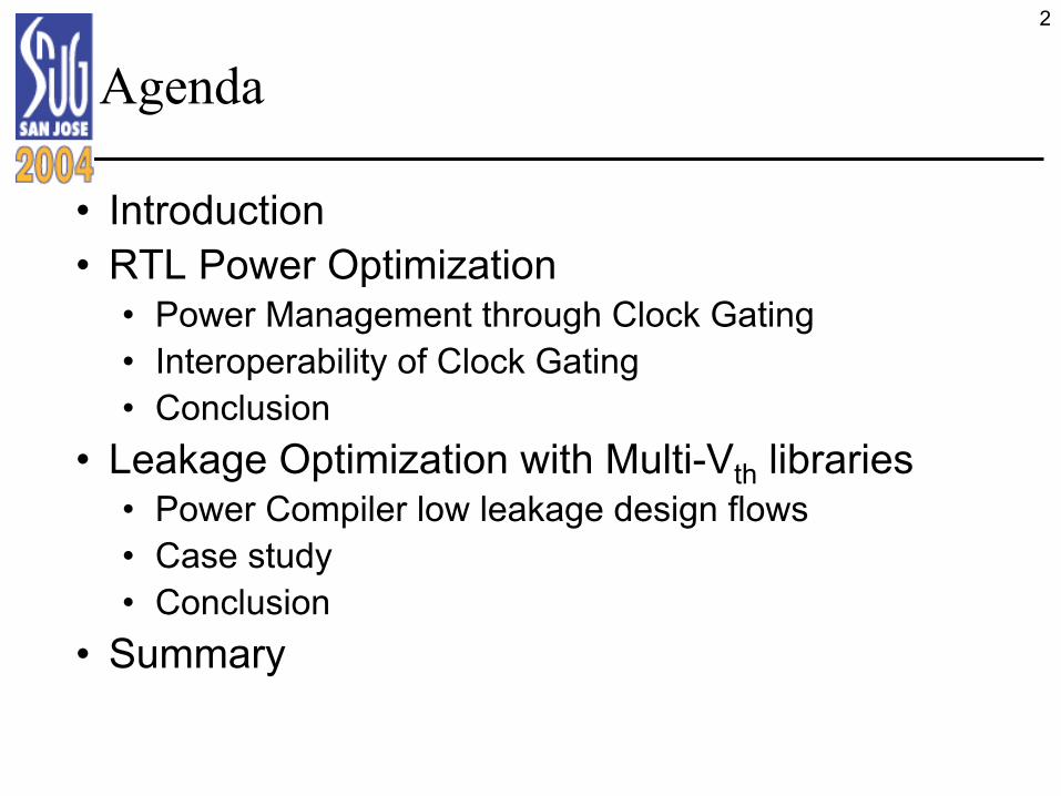
Key Power Management Areas
Low PowerLow Power
Applications• Wireless• Handheld
Concerns• Battery life• Leakage power• Dynamic power
ThermalThermal
Applications• Microprocessors• Graphics/multimedia
Concerns• Thermal management• Packaging, cooling cost• Dynamic & Leakage power
90nm 90nm TechnologyTechnology
Applications• All 90nm designs
Concerns• Chip failure• Voltage-drop• Electromigration
ReliabilityReliability
4
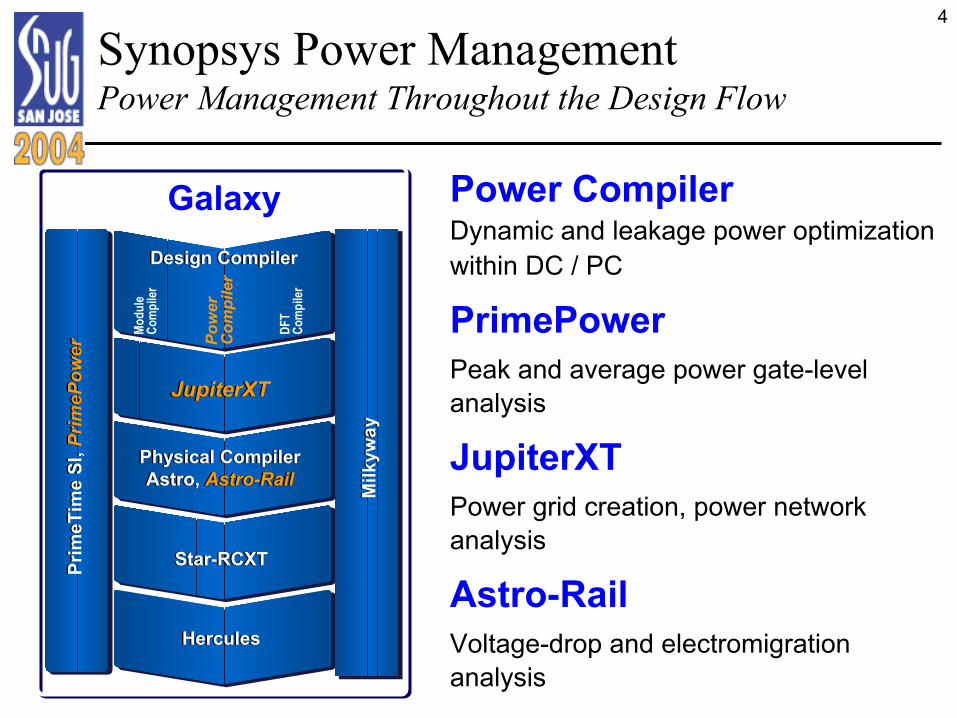
Synopsys Power ManagementPower Management Throughout the Design Flow
Power CompilerDynamic and leakage power optimizationwithin DC / PC
PrimePowerPeak and average power gate-level analysis
JupiterXTPower grid creation, power network analysis
Astro-RailVoltage-drop and electromigrationanalysis
Prim
eTim
e SI
, Prim
ePower
Prim
eTim
e SI
, Prim
ePower
Physical CompilerAstro, Astro-Rail
Physical CompilerAstro, Astro-Rail
JupiterXTJupiterXT
Star-RCXTStar-RCXT
HerculesHercules
Design CompilerDesign Compiler
Milk
yway
Milk
yway
Power
Compiler
DFT
Com
piler
Modu
leCo
mpi
ler
Galaxy
5
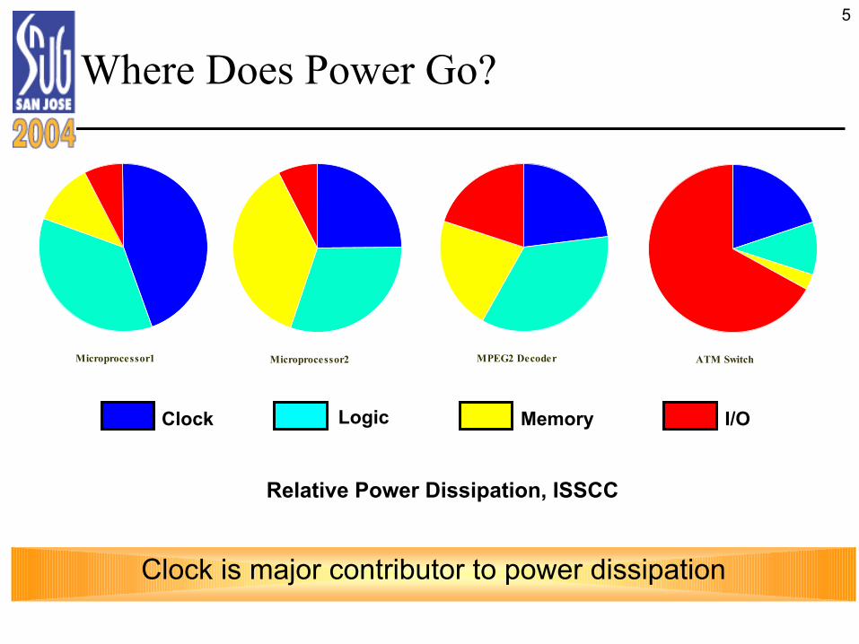
Where Does Power Go?
Clock is major contributor to power dissipation
Relative Power Dissipation, ISSCC
LogicClock Memory I/O
Microprocessor1 Microprocessor2 MPEG2 Decoder ATM Switch
6
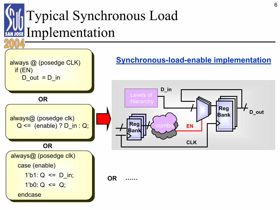
Typical Synchronous Load Implementation
always @ (posedge CLK)if (EN)
D_out = D_in
always @ (posedge CLK)if (EN)
D_out = D_in
always@ (posedge clk)Q <= (enable) ? D_in : Q;
always@ (posedge clk)Q <= (enable) ? D_in : Q;
always@ (posedge clk) case (enable)
1’b1: Q <= D_in;1’b0: Q <= Q;
endcase
always@ (posedge clk) case (enable)
1’b1: Q <= D_in;1’b0: Q <= Q;
endcase
OR
OR
OR ……
Synchronous-load-enable implementation
CLK
D_in
D_out
FF EN
Levels ofHierarchy
RegBank
RegBank
combo
7
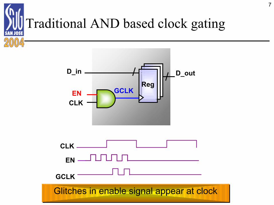
Traditional AND based clock gating
Glitches in enable signal appear at clockGlitches in enable signal appear at clock
CLK
EN
GCLK
D_out
CLK
D_in
EN GCLKReg
8
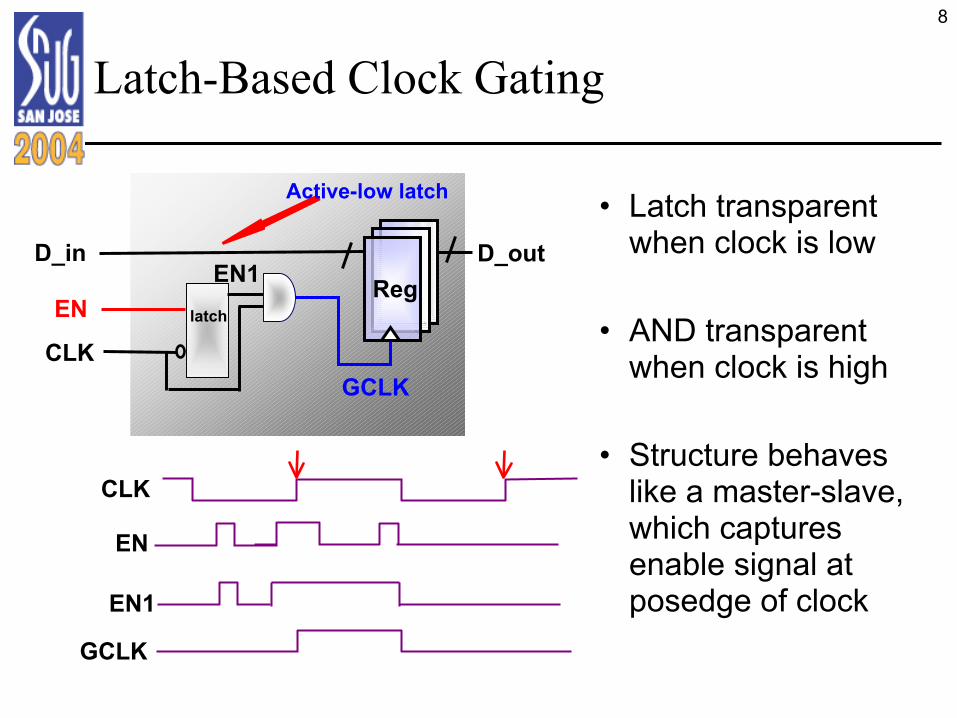
Latch-Based Clock Gating
• Latch transparent when clock is low
• AND transparent when clock is high
• Structure behaves like a master-slave, which captures enable signal at posedge of clock
CLK
EN
GCLK
CLK
D_in
EN
D_out
EN1
GCLK
Reglatch
EN1
Active-low latch
9
CLK@ A
EN
GCLK
CLK@ BEN1
skewdelay
Glitch!
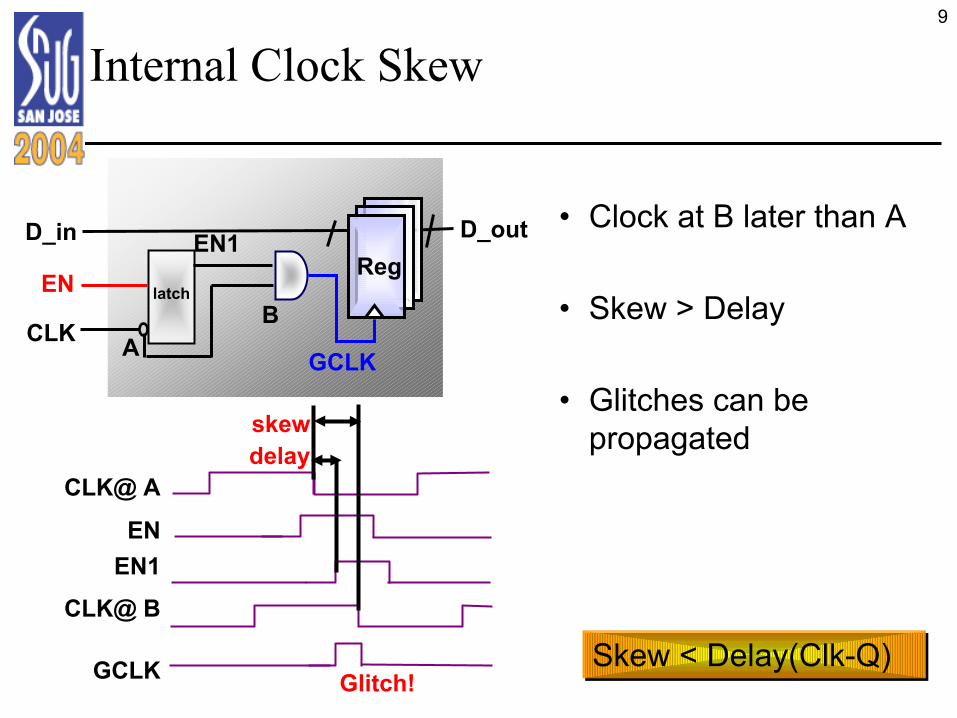
Internal Clock Skew
CLK
D_in
EN
Skew < Delay(Clk-Q)Skew < Delay(Clk-Q)
• Clock at B later than A
• Skew > Delay
• Glitches can be propagated
GCLK
Reglatch
AB
EN1 D_out
10
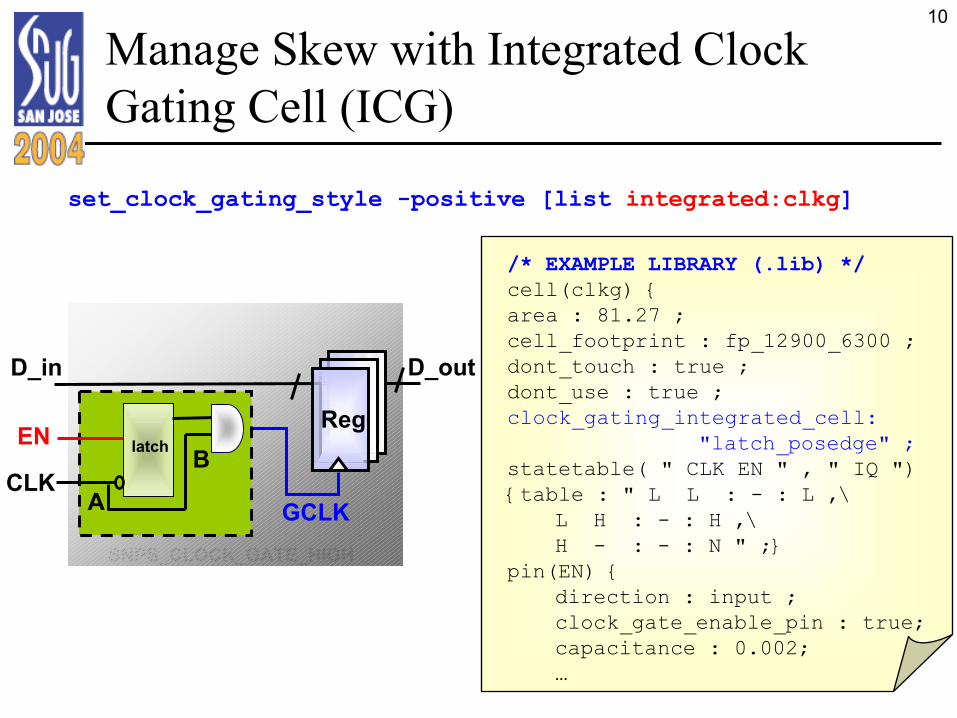
Manage Skew with Integrated Clock Gating Cell (ICG)
/* EXAMPLE LIBRARY (.lib) */cell(clkg) {area : 81.27 ;cell_footprint : fp_12900_6300 ;dont_touch : true ;dont_use : true ;clock_gating_integrated_cell:
"latch_posedge" ;statetable( " CLK EN " , " IQ "){table : " L L : - : L ,\
L H : - : H ,\H - : - : N " ;}
pin(EN) {direction : input ;clock_gate_enable_pin : true;capacitance : 0.002;…
SNPS_CLOCK_GATE_HIGH
set_clock_gating_style -positive [list integrated:clkg]
CLK
D_in
EN
GCLK
Reglatch
AB
D_out
11
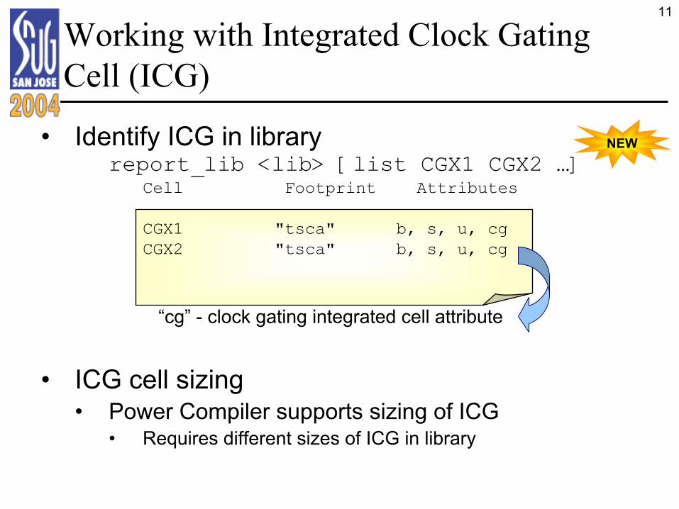
• Identify ICG in library report_lib <lib> [list CGX1 CGX2 …]
Cell Footprint Attributes
CGX1 "tsca" b, s, u, cgCGX2 "tsca" b, s, u, cg
“cg” - clock gating integrated cell attribute
• ICG cell sizing• Power Compiler supports sizing of ICG
• Requires different sizes of ICG in library
Working with Integrated Clock Gating Cell (ICG)
NEW
12
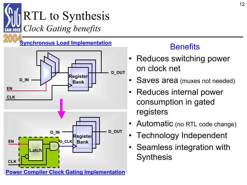
RTL to SynthesisClock Gating benefits
Synchronous Load Implementation
RegisterRegisterBankBank
ENEN
CLKCLK
D_IND_IND_OUTD_OUT
Benefits• Reduces switching power
on clock net• Saves area (muxes not needed)
• Reduces internal power consumption in gated registers
• Automatic (no RTL code change)
• Technology Independent• Seamless integration with
Synthesis
G_CLKG_CLKRegisterRegister
BankBank
LatchLatch
ENEN
CLKCLK
D_IND_IN D_OUTD_OUT
Power Compiler Clock Gating Implementation
13
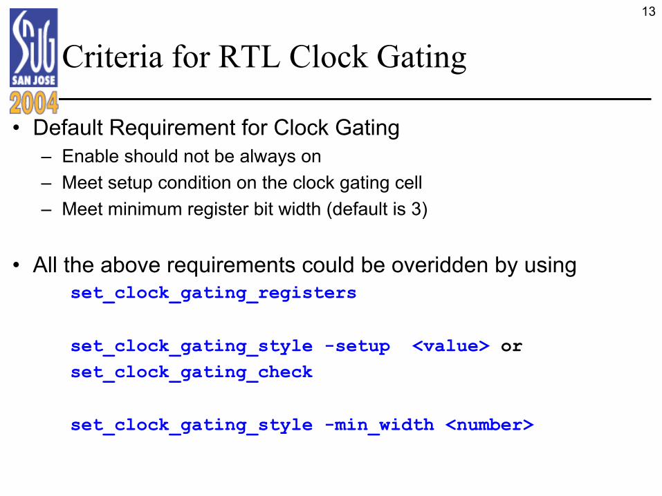
Criteria for RTL Clock Gating
• Default Requirement for Clock Gating – Enable should not be always on– Meet setup condition on the clock gating cell– Meet minimum register bit width (default is 3)
• All the above requirements could be overidden by usingset_clock_gating_registers
set_clock_gating_style -setup <value> orset_clock_gating_check
set_clock_gating_style -min_width <number>
14
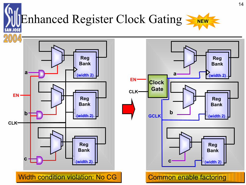
Enhanced Register Clock Gating
Width condition violation: No CGWidth condition violation: No CG Common enable factoringCommon enable factoring
NEW
EN
CLK
a
b
c
RegBank
(width 2)
CLK
ENa
b
c
RegBank
(width 2)
Clock Gate
GCLK
RegBank
(width 2)
RegBank
(width 2)
RegBank
(width 2)
RegBank
(width 2)
15
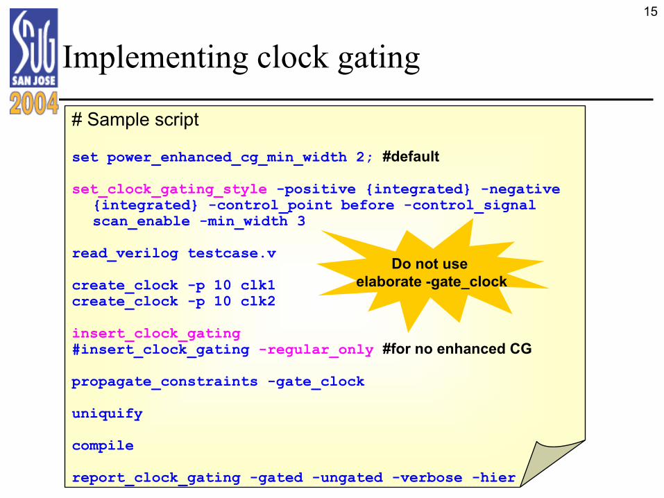
Implementing clock gating
# Sample script
set power_enhanced_cg_min_width 2; #default
set_clock_gating_style -positive {integrated} -negative{integrated} -control_point before -control_signal scan_enable -min_width 3
read_verilog testcase.v
create_clock -p 10 clk1create_clock -p 10 clk2
insert_clock_gating#insert_clock_gating -regular_only #for no enhanced CG
propagate_constraints -gate_clock
uniquify
compile
report_clock_gating -gated -ungated -verbose -hier
Do not use elaborate -gate_clock
16
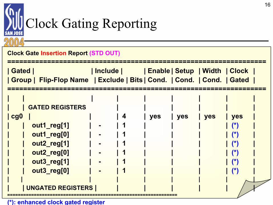
Clock Gating Reporting
Clock Gate Insertion Report (STD OUT)=================================================================| Gated | | Include | | Enable | Setup | Width | Clock || Group | Flip-Flop Name | Exclude | Bits | Cond. | Cond. | Cond. | Gated |=================================================================| | | | | | | | || | GATED REGISTERS | | | | | || cg0 | | | 4 | yes | yes | yes | yes || | out1_reg[1] | - | 1 | | | | (*) || | out1_reg[0] | - | 1 | | | | (*) || | out2_reg[1] | - | 1 | | | | (*) || | out2_reg[0] | - | 1 | | | | (*) || | out3_reg[1] | - | 1 | | | | (*) || | out3_reg[0] | - | 1 | | | | (*) || | | | | | | | || | UNGATED REGISTERS | | | | | | |================================================================(*): enhanced clock gated register
17
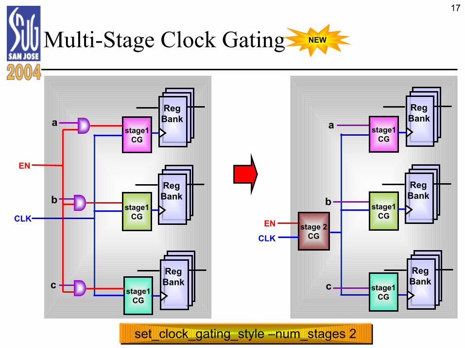
Multi-Stage Clock Gating NEW
set_clock_gating_style –num_stages 2set_clock_gating_style –num_stages 2
stage1CG
stage1CG
RegBank
stage1CG
RegBank
RegBank
a
b
c
EN
CLKstage1
CG
stage1CG
RegBank
RegBank
RegBank
a
b
c
ENCLK
stage 2CG
stage1CG
18
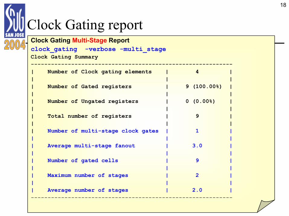
Clock Gating Multi-Stage Reportclock_gating -verbose -multi_stageClock Gating Summary------------------------------------------------------------| Number of Clock gating elements | 4 || | || Number of Gated registers | 9 (100.00%) || | | | Number of Ungated registers | 0 (0.00%) || | || Total number of registers | 9 || | || Number of multi-stage clock gates | 1 || | || Average multi-stage fanout | 3.0 || | || Number of gated cells | 9 || | || Maximum number of stages | 2 || | || Average number of stages | 2.0 |------------------------------------------------------------
Clock Gating report
19
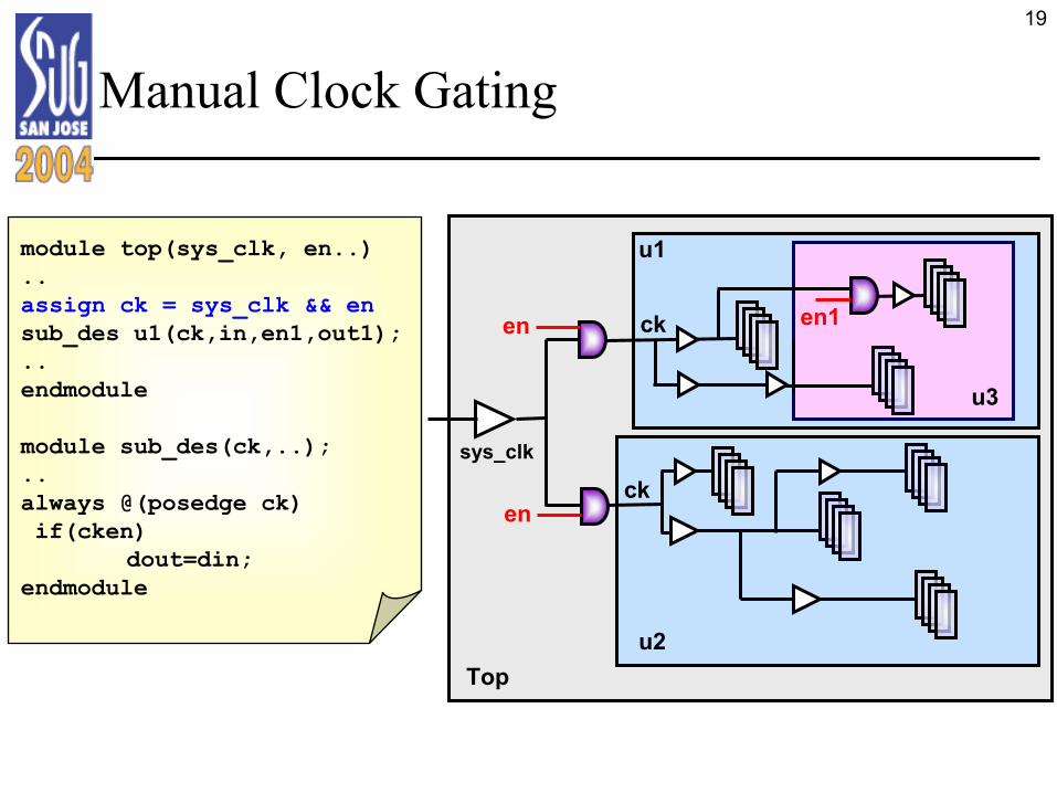
Manual Clock Gating
module top(sys_clk, en..)..assign ck = sys_clk && ensub_des u1(ck,in,en1,out1);..endmodule
module sub_des(ck,..);..always @(posedge ck)if(cken)
dout=din;endmodule
sys_clk
Top
u1
en
u2
ck
ck
u3
en1
en
20
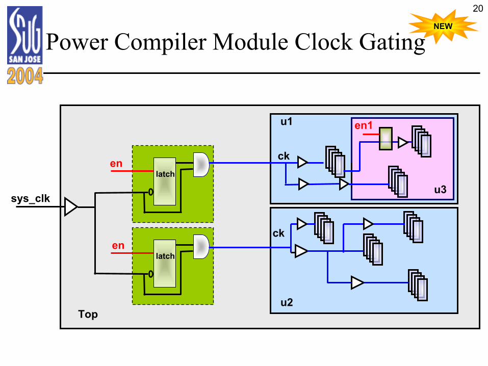
Power Compiler Module Clock Gating
sys_clk
Top
en
NEW
u1
u2
ck
ck
u3latch
latch
en1
en
21
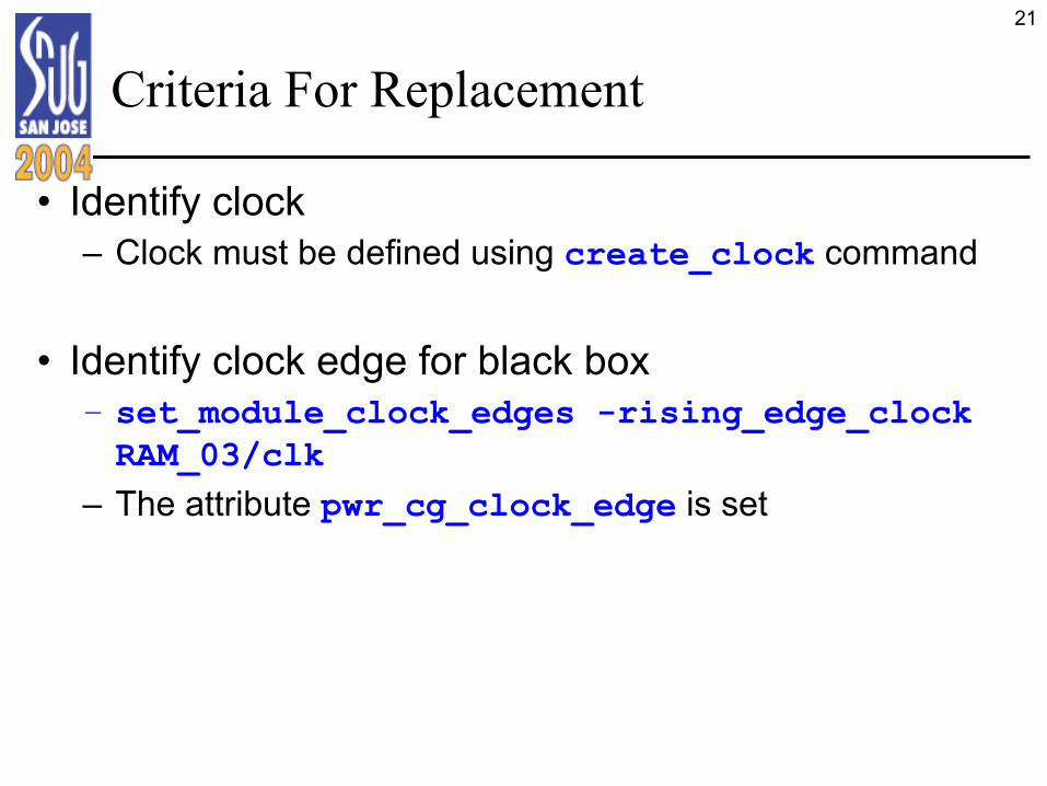
Criteria For Replacement
• Identify clock– Clock must be defined using create_clock command
• Identify clock edge for black box– set_module_clock_edges -rising_edge_clock RAM_03/clk
– The attribute pwr_cg_clock_edge is set
22
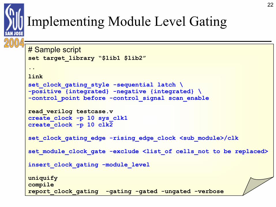
Implementing Module Level Gating
# Sample scriptset target_library “$lib1 $lib2”
..
linkset_clock_gating_style -sequential latch \-positive {integrated} -negative {integrated} \-control_point before -control_signal scan_enable
read_verilog testcase.vcreate_clock -p 10 sys_clk1create_clock -p 10 clk2
set_clock_gating_edge -rising_edge_clock <sub_module>/clk
set_module_clock_gate -exclude <list_of cells_not to be replaced>
insert_clock_gating -module_level
uniquifycompilereport_clock_gating -gating -gated -ungated -verbose
23
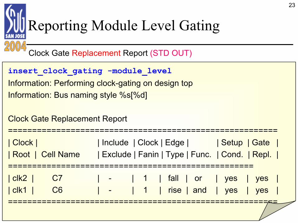
Reporting Module Level Gating
insert_clock_gating -module_level
Information: Performing clock-gating on design topInformation: Bus naming style %s[%d]
Clock Gate Replacement Report========================================================| Clock | | Include | Clock | Edge | | Setup | Gate || Root | Cell Name | Exclude | Fanin | Type | Func. | Cond. | Repl. |===================================================| clk2 | C7 | - | 1 | fall | or | yes | yes || clk1 | C6 | - | 1 | rise | and | yes | yes |========================================================
Clock Gate Replacement Report (STD OUT)
24
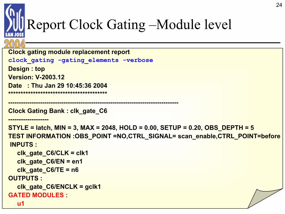
Report Clock Gating –Module level
Clock gating module replacement report clock_gating -gating_elements -verboseDesign : topVersion: V-2003.12Date : Thu Jan 29 10:45:36 2004****************************************--------------------------------------------------------------------------------Clock Gating Bank : clk_gate_C6-------------------STYLE = latch, MIN = 3, MAX = 2048, HOLD = 0.00, SETUP = 0.20, OBS_DEPTH = 5 TEST INFORMATION :OBS_POINT =NO,CTRL_SIGNAL= scan_enable,CTRL_POINT=before INPUTS :
clk_gate_C6/CLK = clk1 clk_gate_C6/EN = en1 clk_gate_C6/TE = n6
OUTPUTS :clk_gate_C6/ENCLK = gclk1
GATED MODULES :u1
25
Agenda
• Introduction • RTL Power Optimization
• Power Management through Clock Gating• Interoperability of Clock Gating • Conclusion
26
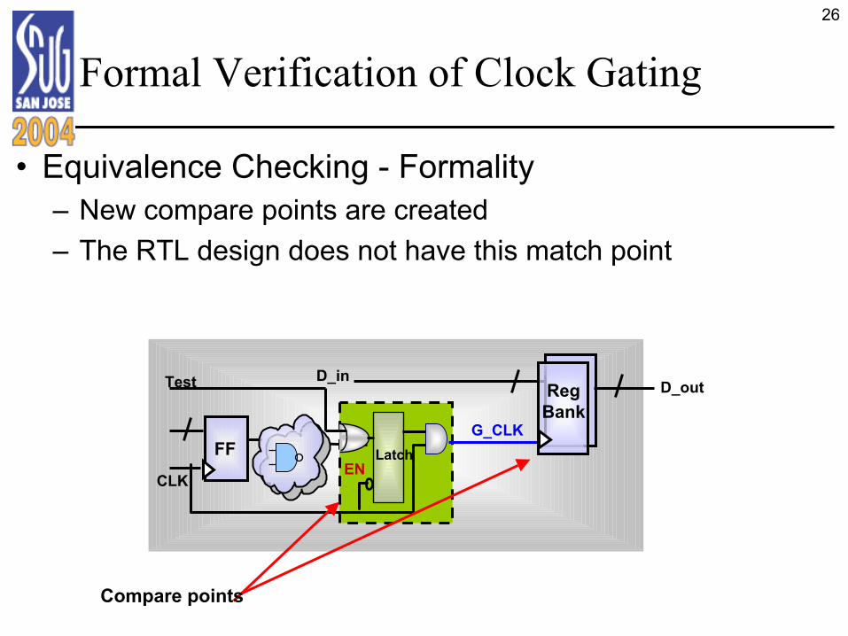
Formal Verification of Clock Gating
• Equivalence Checking - Formality– New compare points are created – The RTL design does not have this match point
D_in
EN
G_CLKLatch
CLK
FF
Compare points
Test RegBank
D_out
27
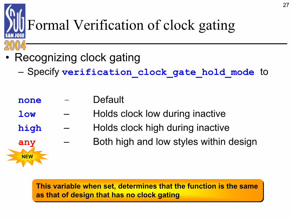
Formal Verification of clock gating
• Recognizing clock gating– Specify verification_clock_gate_hold_mode to
none - Defaultlow – Holds clock low during inactivehigh – Holds clock high during inactiveany – Both high and low styles within design
This variable when set, determines that the function is the sameas that of design that has no clock gatingThis variable when set, determines that the function is the sameas that of design that has no clock gating
NEW
28
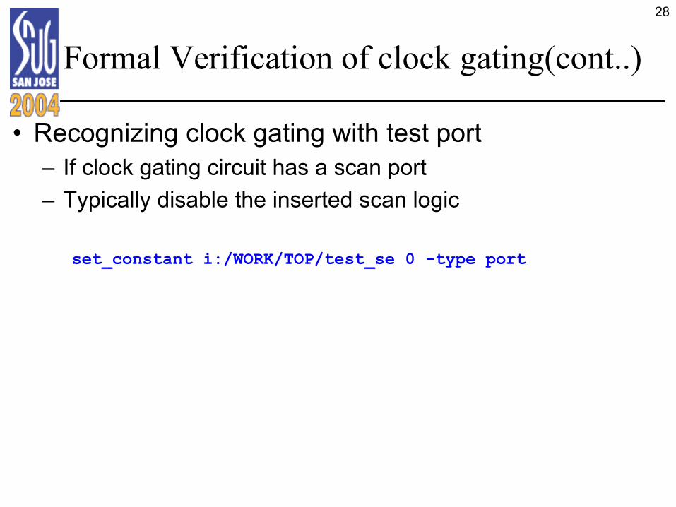
Formal Verification of clock gating(cont..)
• Recognizing clock gating with test port– If clock gating circuit has a scan port– Typically disable the inserted scan logic
set_constant i:/WORK/TOP/test_se 0 -type port
29
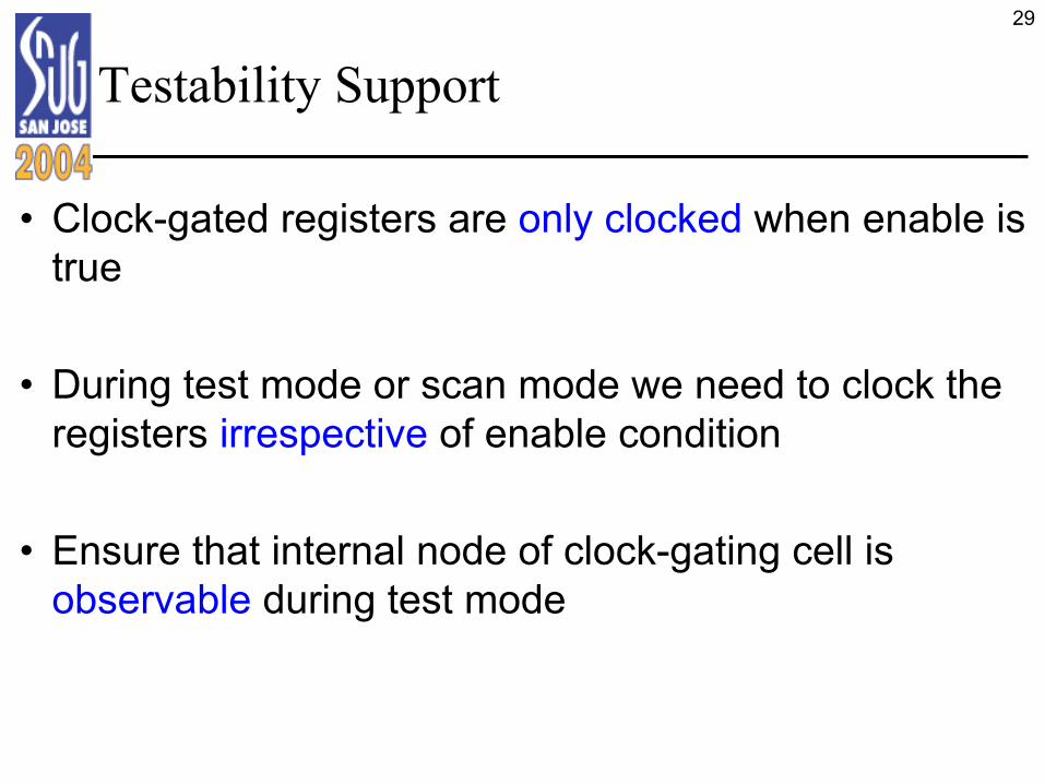
Testability Support
• Clock-gated registers are only clocked when enable is true
• During test mode or scan mode we need to clock the registers irrespective of enable condition
• Ensure that internal node of clock-gating cell is observable during test mode
30
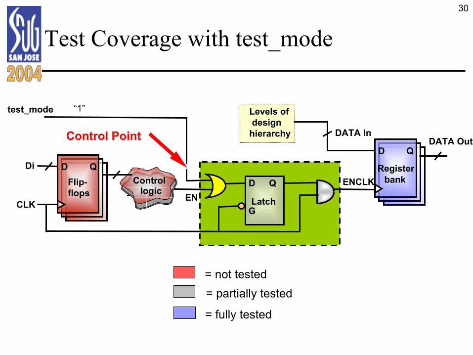
test_mode
ENCLK
Controllogic
Test Coverage with test_mode
Levels of design
hierarchy
D QD Q
D Q
GLatch
DATA In DATA Out
ENCLKRegister
bankFlip-flops
= fully tested
= partially tested= not tested
“1”
Di
Control Point
31
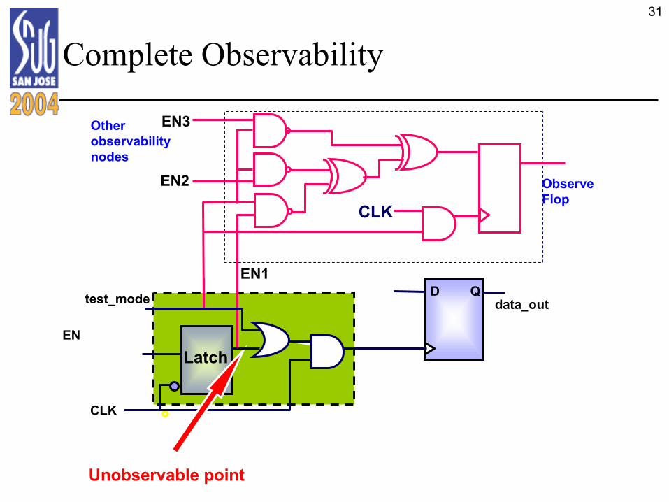
Complete Observability
test_mode
EN
CLK
D Qdata_out
Observe Flop
CLK
Otherobservabilitynodes
Unobservable point
Latch
EN3
EN2
EN1
32
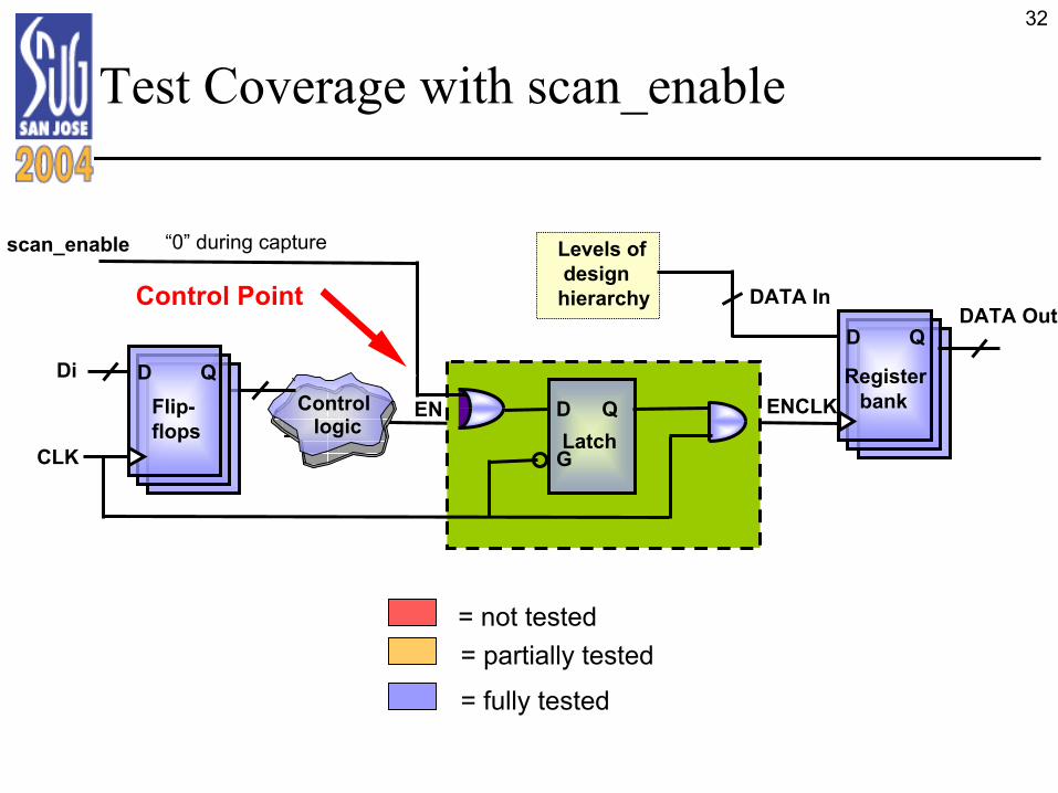
scan_enable
EN
CLK
Controllogic
Test Coverage with scan_enable
Levels of design
hierarchy
D Q
D Q
GLatch
DATA In DATA Out
ENCLKRegister
bank
= fully tested
= partially tested= not tested
D QFlip-flops
“0” during capture
Di
Control Point
33
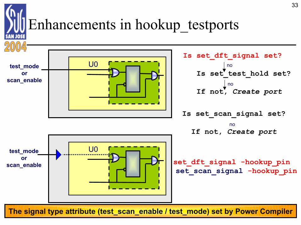
Enhancements in hookup_testports
Is set_dft_signal set?
Is set_test_hold set?
If not, Create port
no
no
set_dft_signal -hookup_pinset_scan_signal -hookup_pin
test_modeor
scan_enable
test_modeor
scan_enable
Is set_scan_signal set?
If not, Create portno
The signal type attribute (test_scan_enable / test_mode) set by Power Compiler
U0
U0
34
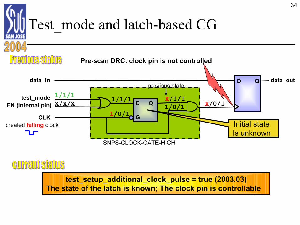
Test_mode and latch-based CG
test_setup_additional_clock_pulse = true (2003.03)The state of the latch is known; The clock pin is controllable
created falling clock
test_modeEN (internal pin)
CLK
1/1/1
1/0/1
SNPS-CLOCK-GATE-HIGH
Pre-scan DRC: clock pin is not controlled
X/1/11/1/1
1/0/1
X/0/1
previous state
X/X/X
Initial stateIs unknown
D Q
G
D Qdata_in data_out
35
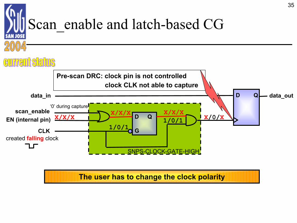
Scan_enable and latch-based CG
The user has to change the clock polarity
created falling clock
scan_enableEN (internal pin)
CLK
1/0/1
SNPS-CLOCK-GATE-HIGH
Pre-scan DRC: clock pin is not controlledclock CLK not able to capture
X/X/XX/X/X
1/0/1
X/0/XX/X/X
‘0’ during capture
D Q
G
D Qdata_in data_out
36
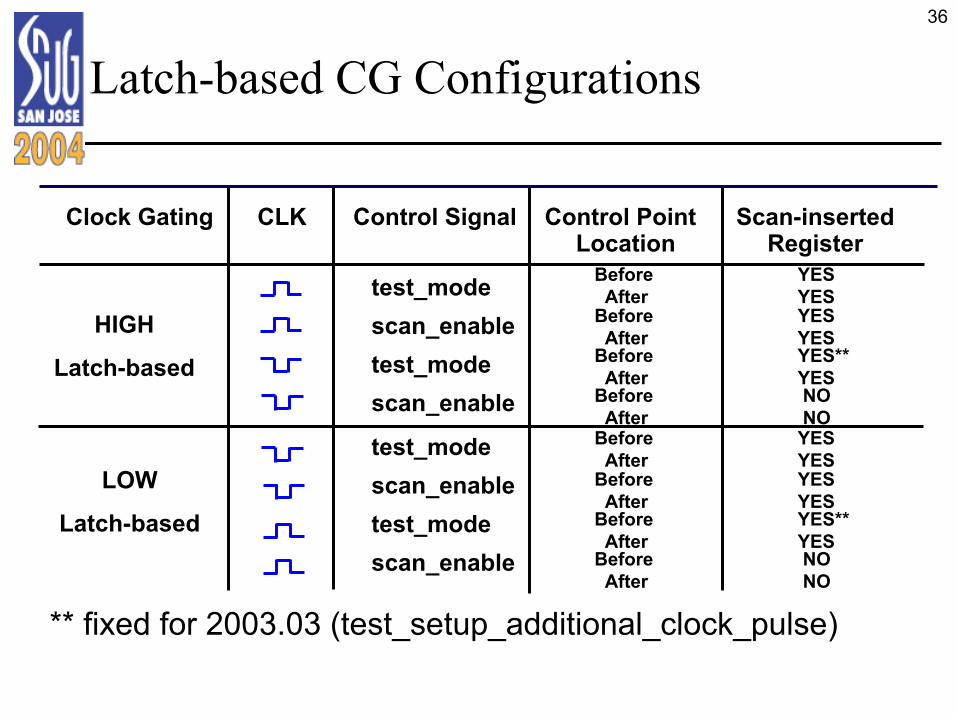
Latch-based CG Configurations
** fixed for 2003.03 (test_setup_additional_clock_pulse)
Clock Gating CLK Control Signal Control Point Scan-insertedLocation Register
test_modescan_enabletest_modescan_enable
test_modescan_enabletest_modescan_enable
LOW
Latch-based
HIGH
Latch-based
Before YESAfter YES
Before YESAfter YES
Before YES**After YES
Before NOAfter NO
Before YESAfter YES
Before YESAfter YES
Before YES**After YES
Before NOAfter NO
37
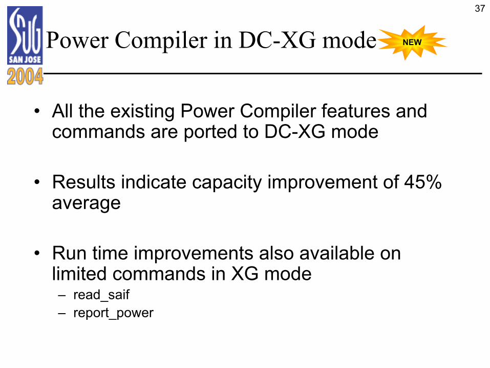
Power Compiler in DC-XG mode
• All the existing Power Compiler features and commands are ported to DC-XG mode
• Results indicate capacity improvement of 45% average
• Run time improvements also available on limited commands in XG mode– read_saif – report_power
NEW
38
Clock-Gating Support
Logic synthesis– Combinatorial setup and hold constraint
generation and checks– Propagate constraints
Formal verification– RTL to gate-level equivalence checking
Back-end support– Clock skew minimization and balancing
Testability– Controllability & observability test logic
XG
39
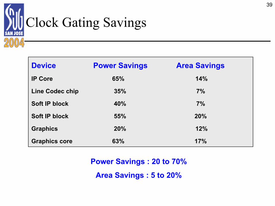
Clock Gating Savings
Device Power Savings Area SavingsIP Core 65% 14%
Line Codec chip 35% 7%
Soft IP block 40% 7%
Soft IP block 55% 20%
Graphics 20% 12%
Graphics core 63% 17%
Power Savings : 20 to 70%
Area Savings : 5 to 20%
Leakage Optimization using Multi-Vth Libraries
Rishi ChawlaPower CAE Team
41
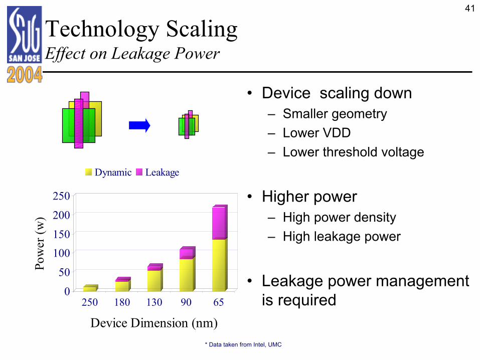
Technology ScalingEffect on Leakage Power
* Data taken from Intel, UMC
0
50
100150
200
250
Pow
er (w
)
250 180 130 90 65
Device Dimension (nm)
Dynamic Leakage
• Device scaling down– Smaller geometry– Lower VDD– Lower threshold voltage
• Higher power– High power density– High leakage power
• Leakage power management is required
42
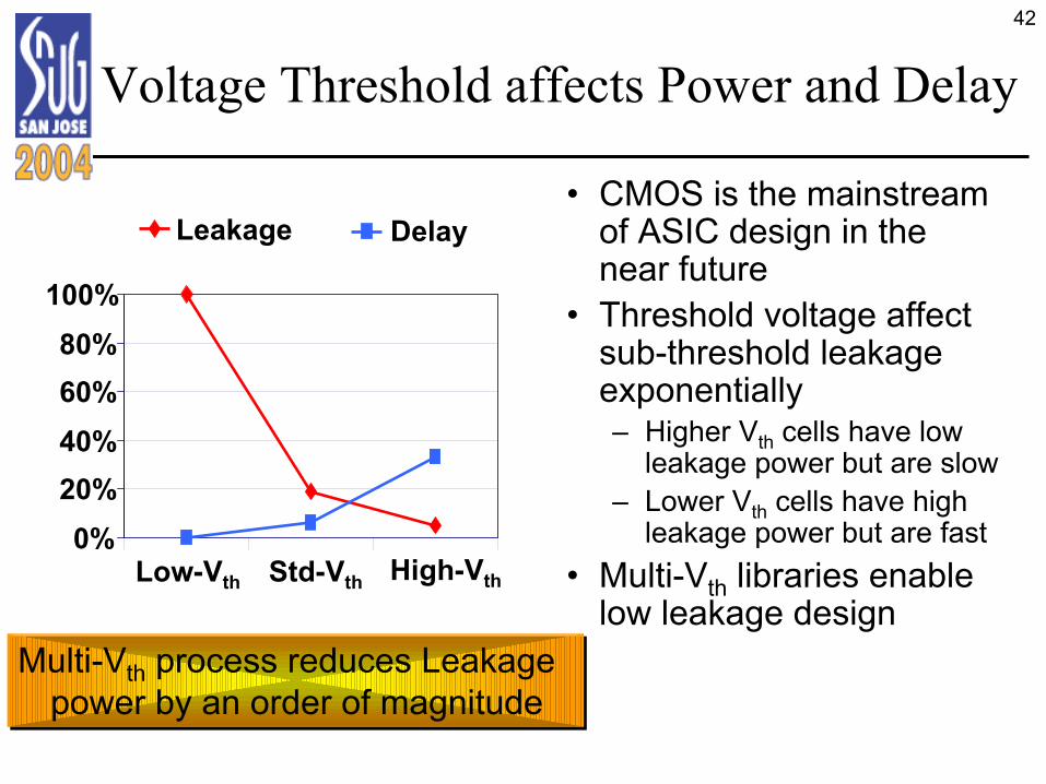
Voltage Threshold affects Power and Delay
• CMOS is the mainstream of ASIC design in the near future
• Threshold voltage affect sub-threshold leakage exponentially– Higher Vth cells have low
leakage power but are slow– Lower Vth cells have high
leakage power but are fast• Multi-Vth libraries enable
low leakage designLow-Vth Std-Vth High-Vth
0%20%40%60%80%
100%
Leakage Delay
Multi-Vth process reduces Leakage power by an order of magnitude
Multi-Vth process reduces Leakage power by an order of magnitude
43
Save Power on Non-Critical paths
Path with High-Vth cellsPath with Low-Vth cells;
• Use Low-Vth cells on critical paths to improve timing
• Use High-Vth cells on non-critical paths to save power
• No impact on timing
Critical path
Non-Critical paths
Timing constraint
A
B
C
D
E
Before Power Optimization
Tim
ing
path
s
Delay
A
B
C
D
E
Leakage reduced
Tim
ing
path
s
Delay
After Power Optimization
44
Improvements in 2003.12 Release
• Performance improved by10X
• Leakage QoR improved upto 20%
• Options to trade-off Performance and QoR
• Pre-Route & Post-Route Power Optimization Flow
45
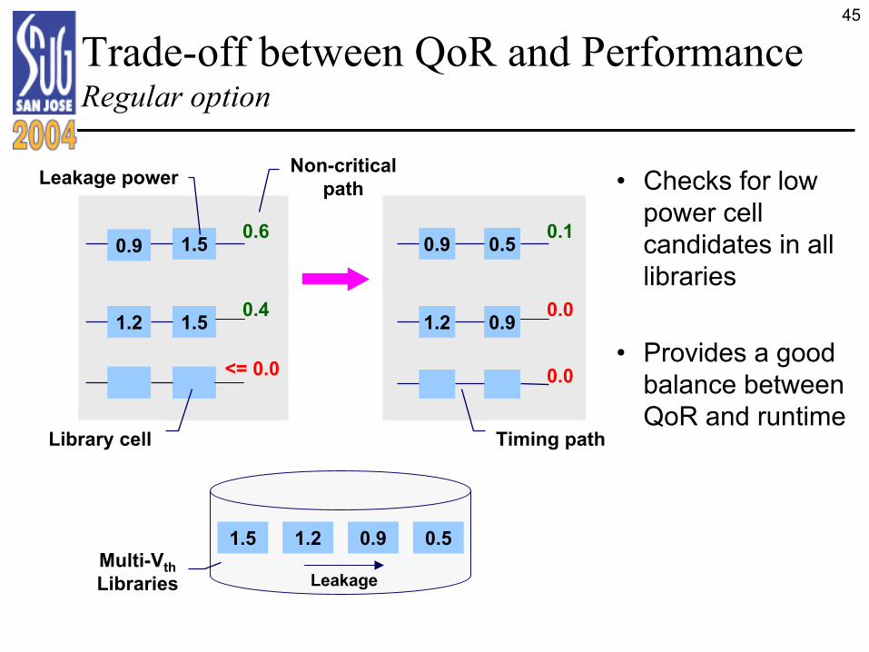
Trade-off between QoR and PerformanceRegular option
1.5 0.5
1.2
1.5
1.5
1.2 0.9
0.90.6
0.4
Non-critical path
Multi-VthLibraries
<= 0.0
Leakage power
Library cell
Leakage
0.9
1.2
0.5
0.9
0.1
0.0
0.0
Timing path
• Checks for low power cell candidates in all libraries
• Provides a good balance between QoR and runtime
46
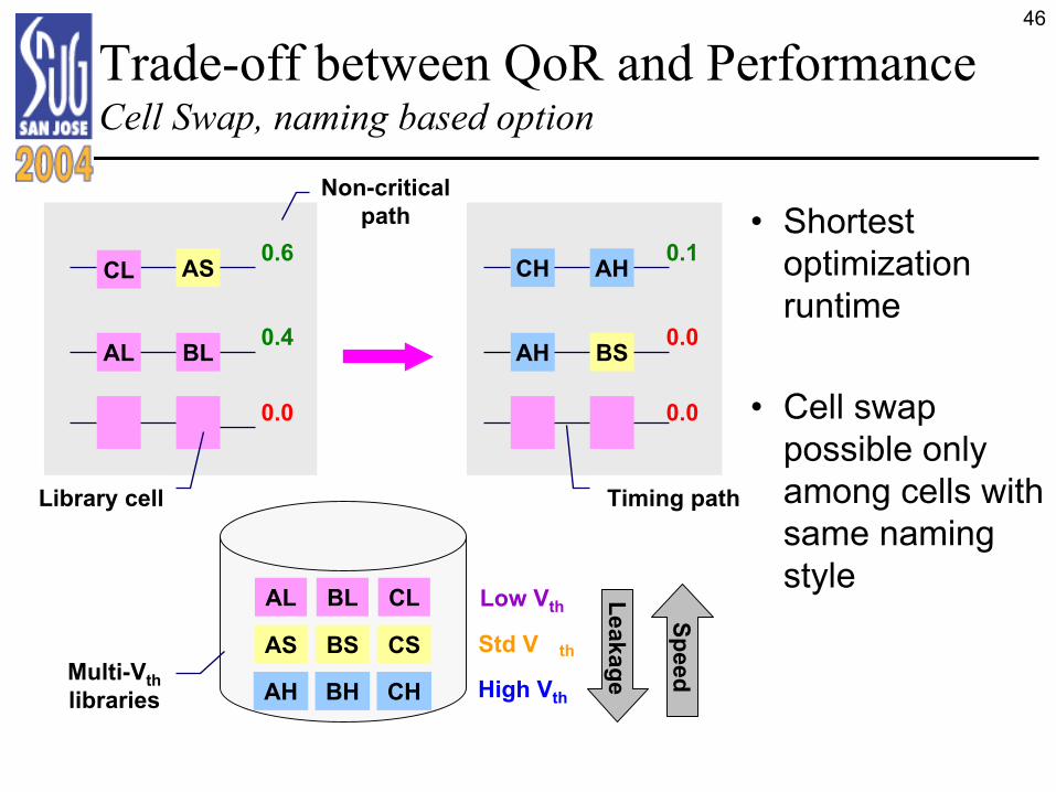
Trade-off between QoR and PerformanceCell Swap, naming based option
• Shortest optimization runtime
• Cell swap possible only among cells with same naming style
AL
AS
AH
AL
AS
BL
BL
BS
BH
CL
CS
CH
Low Vth
Std V
High Vth
CL0.6
0.4
Non-critical path
Multi-Vthlibraries
0.0Speed
Leakage
CH
AH
AH
BS
0.1
0.0
0.0
Timing pathLibrary cell
th
47
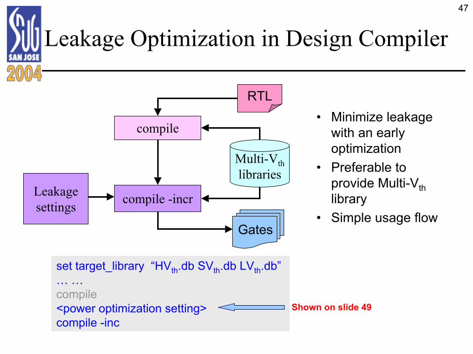
Leakage Optimization in Design Compiler
• Minimize leakage with an early optimization
• Preferable to provide Multi-Vthlibrary
• Simple usage flow
RTL
Multi-Vthlibraries
Gates
Leakagesettings
compile
compile -incr
set target_library “HVth.db SVth.db LVth.db”… …compile<power optimization setting>compile -inc
Shown on slide 49
48
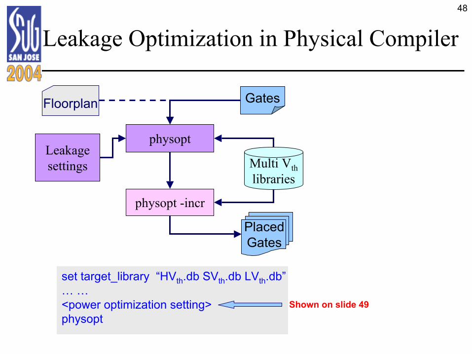
Leakage Optimization in Physical Compiler
Gates
Multi Vthlibraries
PlacedGates
Leakagesettings
Floorplan
physopt
physopt -incr
set target_library “HVth.db SVth.db LVth.db”… …<power optimization setting>physopt
Shown on slide 49
49
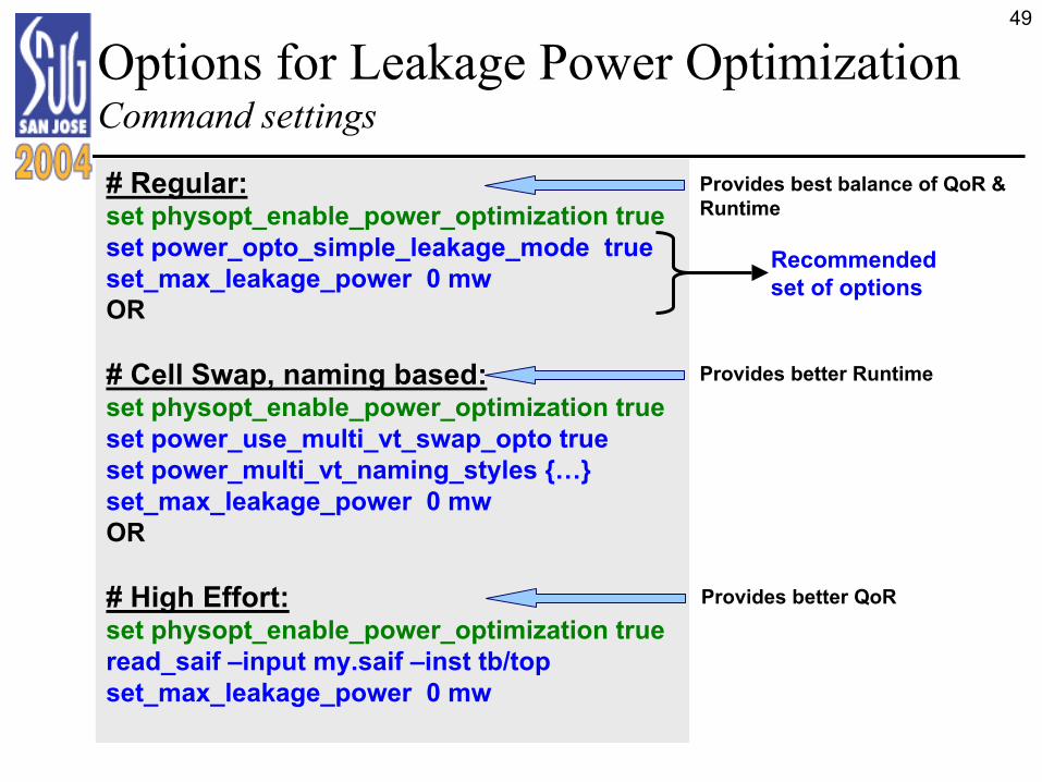
Options for Leakage Power OptimizationCommand settings
# Regular:set physopt_enable_power_optimization trueset power_opto_simple_leakage_mode true set_max_leakage_power 0 mwOR
# Cell Swap, naming based:set physopt_enable_power_optimization trueset power_use_multi_vt_swap_opto trueset power_multi_vt_naming_styles {…}set_max_leakage_power 0 mwOR
# High Effort:set physopt_enable_power_optimization trueread_saif –input my.saif –inst tb/topset_max_leakage_power 0 mw
Recommended set of options
Provides better QoR
Provides better Runtime
Provides best balance of QoR & Runtime
50
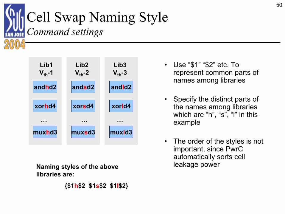
Cell Swap Naming StyleCommand settings
• Use “$1” “$2” etc. To represent common parts of names among libraries
• Specify the distinct parts of the names among libraries which are “h”, “s”, “l” in this example
• The order of the styles is not important, since PwrC automatically sorts cell leakage power
andhd2 andsd2 andld2
xorhd4 xorsd4 xorld4
muxhd3 muxsd3 muxld3
Lib1Vth-1
Lib2Vth-2
Lib3Vth-3
Naming styles of the above libraries are:
{$1h$2 $1s$2 $1l$2}
…… …
51
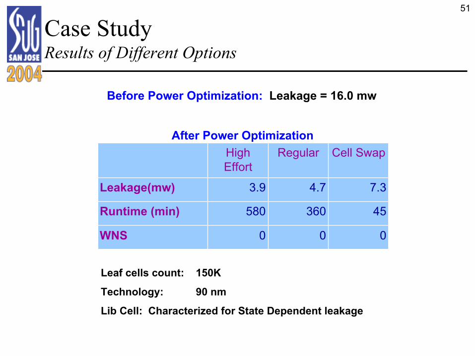
Case StudyResults of Different Options
0
45
7.3
Cell Swap
360580Runtime (min)
00WNS
4.73.9Leakage(mw)
RegularHigh Effort
Leaf cells count: 150K
Technology: 90 nm
Lib Cell: Characterized for State Dependent leakage
Before Power Optimization: Leakage = 16.0 mw
After Power Optimization
52
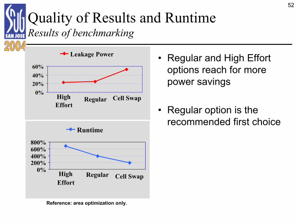
Quality of Results and RuntimeResults of benchmarking
• Regular and High Effort options reach for more power savings
• Regular option is the recommended first choice
0%20%40%60%
HighEffort
Regular Cell Swap
Leakage Power
0%200%400%600%800%
HighEffort
Regular Cell Swap
Runtime
Reference: area optimization only.
53
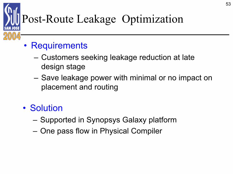
Post-Route Leakage Optimization
• Requirements– Customers seeking leakage reduction at late
design stage– Save leakage power with minimal or no impact on
placement and routing
• Solution– Supported in Synopsys Galaxy platform– One pass flow in Physical Compiler
54
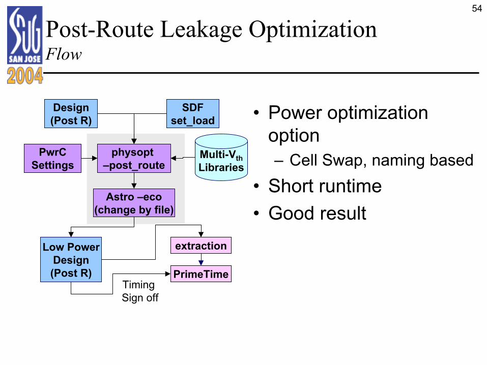
Post-Route Leakage OptimizationFlow
• Power optimization option – Cell Swap, naming based
• Short runtime• Good result
PwrCSettings
Design(Post R)
Multi-VthLibraries
physopt –post_route
Astro –eco(change by file)
extractionLow PowerDesign(Post R)
Timing Sign off
SDFset_load
PrimeTime
55
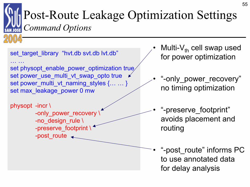
Post-Route Leakage Optimization SettingsCommand Options
set_target_library “hvt.db svt.db lvt.db”… …set physopt_enable_power_optimization trueset power_use_multi_vt_swap_opto trueset power_multi_vt_naming_styles {… … }set max_leakage_power 0 mw
physopt -incr \-only_power_recovery \-no_design_rule \-preserve_footprint \-post_route
• Multi-Vth cell swap used for power optimization
• “-only_power_recovery” no timing optimization
• “-preserve_footprint” avoids placement and routing
• “-post_route” informs PC to use annotated data for delay analysis
56
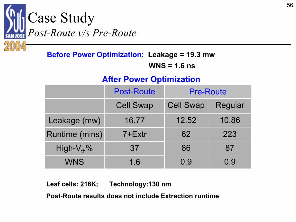
Case StudyPost-Route v/s Pre-Route
Leaf cells: 216K; Technology:130 nm
Post-Route results does not include Extraction runtime
0.90.9878622362
10.8612.52
RegularCell SwapPre-Route
1.6WNS37High-Vth%
7+ExtrRuntime (mins)16.77Leakage (mw)
Cell SwapPost-Route
Before Power Optimization: Leakage = 19.3 mwWNS = 1.6 ns
After Power Optimization
57
Conclusion
• Synopsys recommends to do leakage optimization before routing, using Regular flow– Easy to use– Short runtime– Best result
• Synopsys tools can optimize leakage power for routed designs too– Significantly faster than scripting– Good QoR