Embed Size (px)
Citation preview
RK818 Power Management System
Version 0.3 www.rock-chips.com 1
RK818
Power Management System
Specifications
PRELIMINARY CONFIDENTIAL
V0.3
2014-07-18
Fuzhou Rockchip Electronics Co.Ltd
RK818 Power Management System
Version 0.3 www.rock-chips.com 2
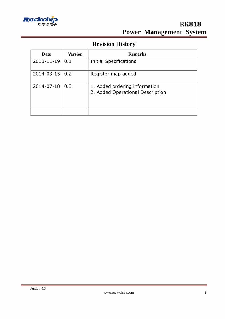
Revision History
Date Version Remarks
2013-11-19 0.1 Initial Specifications
2014-03-15 0.2 Register map added
2014-07-18 0.3 1. Added ordering information
2. Added Operational Description
RK818 Power Management System
Version 0.3 www.rock-chips.com 3
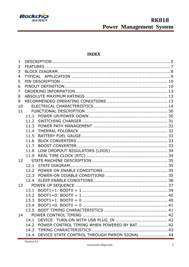
INDEX
1 DESCRIPTION ...................................................................................... 5
2 FEATURES ........................................................................................... 7
3 BLOCK DIAGRAM .................................................................................. 8
4 TYPICAL APPLICATION ........................................................................ 9
5 PIN DESCRIPTION .............................................................................. 10
6 PINOUT DEFINITION ........................................................................... 10
7 ORDERING INFORMATION ................................................................... 13
8 ABSOLUTE MAXIMUM RATINGS ............................................................ 13
9 RECOMMENDED OPERATING CONDITIONS ............................................ 13
10 ELECTRICAL CHARACTERISTICS ...................................................... 14
11 FUNCTIONAL DESCRIPTION ............................................................ 30
11.1 POWER UP/POWER DOWN ......................................................... 30
11.2 SWITCHING CHARGER .............................................................. 31
11.3 POWER PATH MANAGEMENT ...................................................... 32
11.4 THERMAL FOLDBACK ................................................................ 32
11.5 BATTERY FUEL GAUGE ............................................................... 33
11.6 BUCK CONVERTERS .................................................................. 33
11.7 BOOST CONVERTER .................................................................. 33
11.8 LOW DROPOUT REGULATORS (LDOS) ......................................... 34
11.9 REAL TIME CLOCK (RTC) ........................................................... 34
12 STATE MACHINE DESCRIPTION ....................................................... 35
12.1 STATE DIAGRAM ....................................................................... 35
12.2 POWER ON ENABLE CONDITIONS ............................................... 35
12.3 POWER-ON DISABLE CONDITIONS ............................................. 35
12.4 SLEEP ENABLE CONDITIONS ...................................................... 36
13 POWER UP SEQUENCE ................................................................... 37
13.1 BOOT1=1: BOOT0 = 1 .............................................................. 39
13.2 BOOT1=0: BOOT0 = 1 .............................................................. 40
13.3 BOOT1=1: BOOT0 = 0 .............................................................. 40
13.4 BOOT1=0: BOOT0 = 0 .............................................................. 41
13.5 BOOT TIMING CHARACTERISTICS .............................................. 41
14 POWER CONTROL TIMING .............................................................. 42
14.1 DEVICE TURN-ON WITH USB PLUG_IN ...................................... 42
14.2 POWER CONTROL TIMING WHEN POWERED BY BAT ...................... 42
14.3 TIMING CHARACTERISTICS ....................................................... 43
14.4 DEVICE STATE CONTROL THROUGH PWRON SIGNAL .................... 44
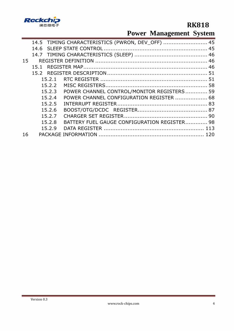
RK818 Power Management System
Version 0.3 www.rock-chips.com 4
14.5 TIMING CHARACTERISTICS (PWRON, DEV_OFF) .......................... 45
14.6 SLEEP STATE CONTROL ............................................................. 45
14.7 TIMING CHARACTERISTICS (SLEEP) ........................................... 46
15 REGISTER DEFINITION .................................................................. 46
15.1 REGISTER MAP ......................................................................... 46
15.2 REGISTER DESCRIPTION ........................................................... 51
15.2.1 RTC REGISTER ............................................................... 51
15.2.2 MISC REGISTERS ............................................................ 58
15.2.3 POWER CHANNEL CONTROL/MONITOR REGISTERS ............. 59
15.2.4 POWER CHANNEL CONFIGURATION REGISTER ................... 68
15.2.5 INTERRUPT REGISTER ..................................................... 83
15.2.6 BOOST/OTG/DCDC REGISTER......................................... 87
15.2.7 CHARGER SET REGISTER ................................................. 90
15.2.8 BATTERY FUEL GAUGE CONFIGURATION REGISTER ............. 98
15.2.9 DATA REGISTER ........................................................... 113
16 PACKAGE INFORMATION .............................................................. 120
RK818 Power Management System
Version 0.3 www.rock-chips.com 5
1 DESCRIPTION
The RK818 is a complex power-management integrated circuit (PMIC) for multi-core system
applications powered by a Li-ion or a Li-ion polymer battery cell, or by a 5V input either from
an USB port or from an adaptor. The RK818 can provide a complete power management
solution with very few external components.
The RK818 provides four configurable synchronous step-down converters and one
synchronous step-up converter with current capability up to 4A and 2.5A, respectively. The
device also contains 9 LDO regulators, one linear switch, one switch-mode charger, a
battery fuel gauge, and the power path management function. Power-up/power-down
controller is configurable and can support any customized power-up/power-down sequences
(OTP based). A real-time clock (RTC) is also integrated to provide a 32-kHz output buffer,
and real time function. The RK818 supports 32-kHz clock generation based on a crystal
oscillator.
The switch-mode charger, together with the power path controller integrated in the RK818,
allows supplying power to the loads while it is charging the battery. The charger provides
functions such as input current limiting, trickle current charging, constant current
(CC)/constant voltage (CV) charging, charging termination, charging over time protection,
etc. All these functions can be conveniently configured through the I2C digital interface. The
input current limit can be set to maximum 3A to accommodate a power adaptor as the input
supply. When an input current limiting is triggered, the power path controller will distribute the
input power in a way that the loads have the higher priority than the battery to take the input
power. The difference between the input and output power will be used to charge the battery.
In a case that the output power required by the loads exceeds the input power, the power
path controller will automatically turn on the battery switch so that the battery can supply
extra power to the loads together with the input supply. A “battery fuel gauge” is also
integrated in the RK818. Using the proprietary algorithms and the sensed battery current and
voltage, the gauge can accurately calculate the battery capacity based on the
charging/discharging characteristics of the battery preloaded in the system. The gauge then
sends the battery capacity information to the processor through the I2C interface. Other
functions that the charger provides includes tiny current charging for an over discharged
battery, or so called “dead battery”, battery temperature monitoring, safe charging timer and
RK818 Power Management System
Version 0.3 www.rock-chips.com 6
over temperature shut down.
The RK818 can dynamically adjust the output voltage of each DC-DC converter, as required
by the processor based on the processor’s operation status so as to maximize the system
efficiency. The output voltages of most channels can be configured through the I2C interface.
The inputs of all channels have soft start function, which greatly reduces the inrush current at
the startup. The frequency compensations of all the control loops are implemented internally
to eliminate external compensation components.
The 2MHz switching frequency allows small size inductors to be used for both buck and
boost converters. Also, as all the power switches are integrated on chip, no external power
switches and Schottky diodes are needed, which reduces the system cost significantly.
The RK818 is available in a QFN68 7.0 mm x 7.0 mm package, with a 0.35-mm pin pitch.
RK818 Power Management System
Version 0.3 www.rock-chips.com 7
2 FEATURES
Input range: 3.8V - 6V for USB input; 2.7V - 4.5V for BAT input
Switch mode Li-ion battery charger providing charging current up to 3A.
Power path controller with 5A current path.
Accurate battery fuel gauge.
Real time clock(RTC)
Low standby current of less than 40uA (at 32KHz clock frequency)
2MHz switching frequency for the buck converters
1MHz switching frequency for the boost converter
Fast transient response due to the current mode architecture
Internal frequency compensation and soft start
Programmable output voltage and power up/down sequence through I2C interface
Proprietary circuit architecture achieving high efficiency
Internal discharge path in off state for BUCs and LDOs
Power channels: Ch1: Synchronous buck converter, 4A max Ch 2: Synchronous buck converter, 4A max Ch 3: Synchronous buck converter, 2.5A max Ch 4: Synchronous buck converter, 2.5A max Ch5: Synchronous boost converter, 2.5A max
Ch6-7, Ch9 and Ch11: LDOs, 150mA max
Ch8: Low noise, high PSRR LDO ,100mA max Ch10, 12,14: LDOs, 300mA max Ch13: LDO, 400mA max
Ch15: Low Rdson switch,0.15ohm(Vgs=3V)
Ch16: HDMI5V switch, 80mA max
Ch17:OTG switch,800mA max
Fixed and programmable power up/down sequences Package: 7mmx7mm QFN68
RK818 Power Management System
Version 0.3 www.rock-chips.com 8
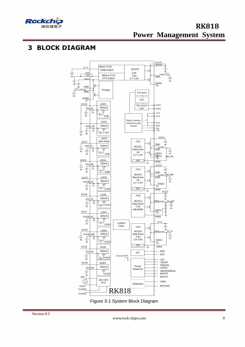
3 BLOCK DIAGRAM
RK818
USB
SYS
SYS
BAT
BAT
SNSP
SNSN
TS2
H_5V
Exposed GND
Bat current
sense
MIDU
Battery monitor
and power path
controlTS1
BUCK1
Step-Down
4A
0.7~1.5V
DAC
SW1
GND1
BUCK3
Step-Down
2.5A
adjustable
VCC3
SW3
GND3
BUCK4
Step-Down
2.5A
1.8~3.6V
DAC
SW4
GND4
LDO3
1/2MHz
Clock
LDO2
LDO4
LDO5
32K OSC
RTC
CLK321
XIN
XOUT
I2CSDA
SCK
INTSLEEP
PWRON
NRESPWRON
150mA
100mA
150mA
300mA
150mA
VCC6 LDO1
150mA
Vdd_arm
BOOT0
BOOT1
VREF
REFGND
Power
Sequence
LDO9
300mA
Switch
300mA
LDO6
LDO7
300mA
400mA
LDO8
Vcc_tp
Vcca_33
Vcc_25
Vcc28_cif
Vcc_12
Vcc_lcd
Vcc_sd
Vdd_11
Vcc_io
Vcc_ddr
Vcc18_cif
Vcc33_wifi
LDO3
(low noise)
VCC8
VCC7
VFB1
VFB3
VFB4
CLK322
Reference
CH1
CH3
CH4
CH6
CH7
CH8
CH13
CH9
CH10
CH11
CH12
CH14
CH15
VCC7
VCC8
SW1
GND1
BUCK2
Step-Down
4A
0.7~1.5V
DAC
VCC2
SW2
GND2
Vdd_logic
VFB2
CH2
SW2
VCC1
VCC7
VCC8
VCC9
VCC9
ADC
Fuel gause
SW5
GND5
BOOST
SYS
VCC4
ChargerSW6
GND6
SW6SYS
VDDIO
BOOST
HDMI Switch
800mA CH17CH5
2.5A
4.7~5.4V
80mA CH16
USB
OTG Switch
BOOST
Figure 3-1 System Block Diagram
RK818 Power Management System
Version 0.3 www.rock-chips.com 9
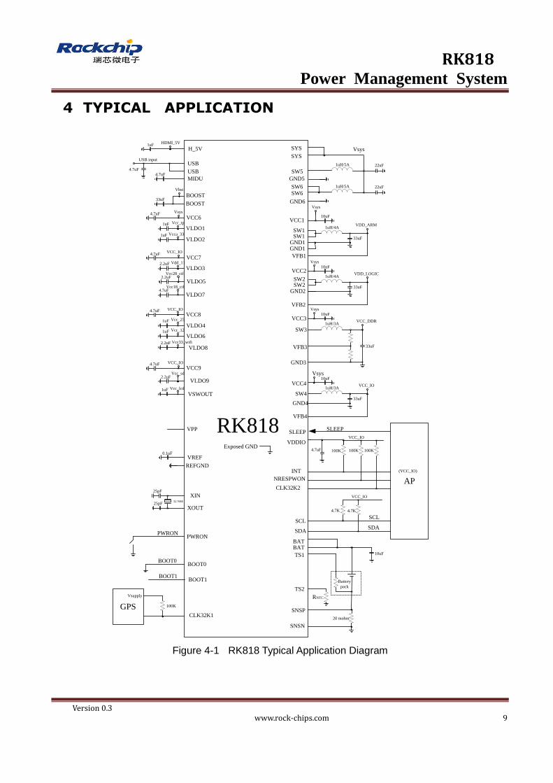
4 TYPICAL APPLICATION
VCC64.7uF Vsys
VLDO11uF
VLDO21uF Vcca_33
XIN25pF
25pF
XOUT
32.768K
SW1SW1
1uH/4A
GND133uF
GND1
VDD_ARM
VFB1
1uH/4A
33uF
VDD_LOGIC
VFB2
SW3
VFB3
GND3
SW4
GND4
VFB4
VCC110uF
Vsys
VCC210uF
Vsys
1uH/3A
33uF
VCC_DDR
10uF
Vsys
VCC3
VCC41uH/3A
33uF
VCC_IO
10uF
Vcc_tp
VCC74.7uF
VCC_IO
VLDO32.2uF
VLDO74.7uF
Vcc18_cif
Vdd_11
VCC84.7uF
VLDO9
2.2uF
Vcc_sd
VCC94.7uF
VLDO41uF Vcc_25
VLDO61uF Vcc_12
VLDO8
2.2uF
Vcc33_wifi
VSWOUT1uF Vcc_lcd
CLK32K2
VREF0.1uF
REFGND
VPPSLEEP
SLEEP
INT
NRESPWON
PWRONPWRON
BOOT0BOOT0
BOOT1BOOT1
AP
(VCC_IO)
VCC_IO
VCC_IO
RK818
SCL
4.7K
SDA
4.7K
SCL
SDA
100K 100K 100K
VCC_IO
VCC_IO
Exposed GND
BATBAT
10uF
20 mohm
SNSP
SNSN
TS1
CLK32K1
GPS 100K
Vsupply
USBUSB input
SYS
SYS
Vsys
BOOST33uF
4.7uF
MIDU4.7uF
SW5
GND5
1uH/5A 22uF
H_5V
TS2
1uFHDMI_5V
RNTC
SW2SW2
GND2
VLDO52.2uF
Vcc28_cif
USB
SW6SW6
GND6
1uH/5A 22uF
Vsys
VDDIO
4.7uF
BOOSTVbst
Battery
pack
Figure 4-1 RK818 Typical Application Diagram
RK818 Power Management System
Version 0.3 www.rock-chips.com 10
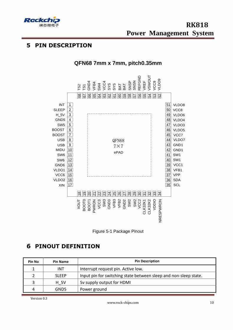
5 PIN DESCRIPTION
QFN68 7mm x 7mm, pitch0.35mm
1
2
3
4
5
6
7
8
10
11
12
13
14
15
9
16
17
18
19
20
21
22
23
24
25
27
28
29
30
31
32
26
33
34
51
50
49
48
47
46
45
44
42
41
40
39
38
37
43
36
35
68
67
66
65
64
63
62
61
59
58
57
56
55
54
60
53
52
QFN68 7×7
VLDO6
VCC7
VLDO3
VPP
VS
WO
UT
VCC8
VC
C9
VLDO4
VLDO5
VLDO8
BO
OT
0
VLDO7
SLEEP
INT
VF
B3
GN
D3
VC
C3
SW
3V
CC
4
SW
4
VF
B4
GN
D4
VR
EF
SDA
SCL
NR
ES
PW
RO
N
TS
2
VC
C2
SW
2
SW
2
GN
D2
VF
B2
VLDO1
VCC6
VLDO2
CL
K3
2K
1
CL
K3
2K
2
RE
FG
ND
VCC1
SW1
SW1
GND1
GND1
VFB1
PW
RO
N
ePAD
VL
DO
9
BO
OT
1
TS
1
SN
SN
SN
SP
BA
T
BA
T
SY
S
SY
S
XO
UT
XIN
H_5V
USB
MIDU
SW5
GND5
BOOST
BOOST
USB
SW6
SW6
GND6
VD
DIO
Figure 5-1 Package Pinout
6 PINOUT DEFINITION
Pin No Pin Name Pin Description 1 INT Interrupt request pin. Active low.
2 SLEEP Input pin for switching state between sleep and non-sleep state.
3 H_5V 5v supply output for HDMI
4 GND5 Power ground
RK818 Power Management System
Version 0.3 www.rock-chips.com 11
5 SW5 Switch output
6,7 BOOST BOOST output
8,9 USB Power input from USB
10 MIDU Middle point of USB power supply
11:12 SW6 Switch output
13 GND6 Power ground
14 VLDO1 LDO1 output
15 VCC6 Power supply for LDO
16 VLDO2 LDO2 output
17 XIN 32.768KHz crystal oscillator input
18 XOUT 32.768KHz crystal oscillator output
19 BOOT0 Boot sequence selection, low bit
20 BOOT1 Boot sequence selection, high bit
21 PWRON Power on or power off enable pin, active low, internal 100K pull high
to power supply
22 VCC3 Power supply for DCDC3
23 SW3 Switch output of DCDC3
24 GND3 Power ground for DCDC3
25 VFB3 feedback voltage for DCDC3
26 VFB2 DCDC2 output voltage feedback input
27 GND2 Power ground for DCDC2
28,29 SW2 Switch output of DCDC2
30 VCC2 Power supply for DCDC2
31 CLK32K1 32.768K clock1 output, open drain,
32 CLK32K2 32.768K clock2 output, open drain,
33 VDDIO Power supply for IO
34 NRESPWON Reset pin after power on, active low
35 SCL Clock input of I2C
36 SDA Data input/output of I2C
37 VPP Power supply for testing, floating in the application
38 VFB1 DCDC1 output voltage feedback input
39 VCC1 Power supply for DCDC1
40:41 SW1 Switch output of DCDC1
42,43 GND1 Power ground for DCDC1
44 VLDO7 LDO7 output
45 VCC7 Power supply for LDO
46 VLDO5 LDO5 output
RK818 Power Management System
Version 0.3 www.rock-chips.com 12
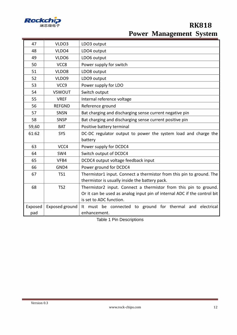
47 VLDO3 LDO3 output
48 VLDO4 LDO4 output
49 VLDO6 LDO6 output
50 VCC8 Power supply for switch
51 VLDO8 LDO8 output
52 VLDO9 LDO9 output
53 VCC9 Power supply for LDO
54 VSWOUT Switch output
55 VREF Internal reference voltage
56 REFGND Reference ground
57 SNSN Bat charging and discharging sense current negative pin
58 SNSP Bat charging and discharging sense current positive pin
59,60 BAT Positive battery terminal
61:62 SYS DC-DC regulator output to power the system load and charge the
battery
63 VCC4 Power supply for DCDC4
64 SW4 Switch output of DCDC4
65 VFB4 DCDC4 output voltage feedback input
66 GND4 Power ground for DCDC4
67 TS1 Thermistor1 input. Connect a thermistor from this pin to ground. The
thermistor is usually inside the battery pack.
68 TS2 Thermistor2 input. Connect a thermistor from this pin to ground.
Or it can be used as analog input pin of internal ADC if the control bit
is set to ADC function.
Exposed
pad
Exposed ground It must be connected to ground for thermal and electrical
enhancement.
Table 1 Pin Descriptions
RK818 Power Management System
Version 0.3 www.rock-chips.com 13
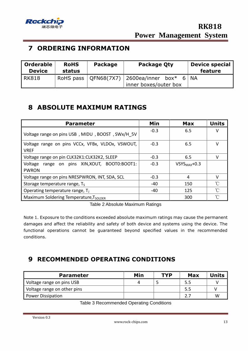
7 ORDERING INFORMATION
Orderable
Device
RoHS
status
Package Package Qty Device special
feature
RK818 RoHS pass QFN68(7X7) 2600ea/inner box* 6
inner boxes/outer box
NA
8 ABSOLUTE MAXIMUM RATINGS
Parameter Min Max Units
Voltage range on pins USB,MIDU,BOOST,SWx/H_5V -0.3 6.5 V
Voltage range on pins VCCx, VFBx, VLDOx, VSWOUT,
VREF
-0.3 6.5 V
Voltage range on pin CLK32K1:CLK32K2, SLEEP -0.3 6.5 V
Voltage range on pins XIN,XOUT, BOOT0:BOOT1:
PWRON
-0.3 VSYSMAX+0.3
Voltage range on pins NRESPWRON, INT, SDA, SCL -0.3 4 V
Storage temperature range, TS -40 150
Operating temperature range, TJ -40 125
Maximum Soldering Temperature,TSOLDER 300
Table 2 Absolute Maximum Ratings
Note 1. Exposure to the conditions exceeded absolute maximum ratings may cause the permanent
damages and affect the reliability and safety of both device and systems using the device. The
functional operations cannot be guaranteed beyond specified values in the recommended
conditions.
9 RECOMMENDED OPERATING CONDITIONS
Parameter Min TYP Max Units
Voltage range on pins USB 4 5 5.5 V
Voltage range on other pins 5.5 V
Power Dissipation 2.7 W
Table 3 Recommended Operating Conditions
RK818 Power Management System
Version 0.3 www.rock-chips.com 14
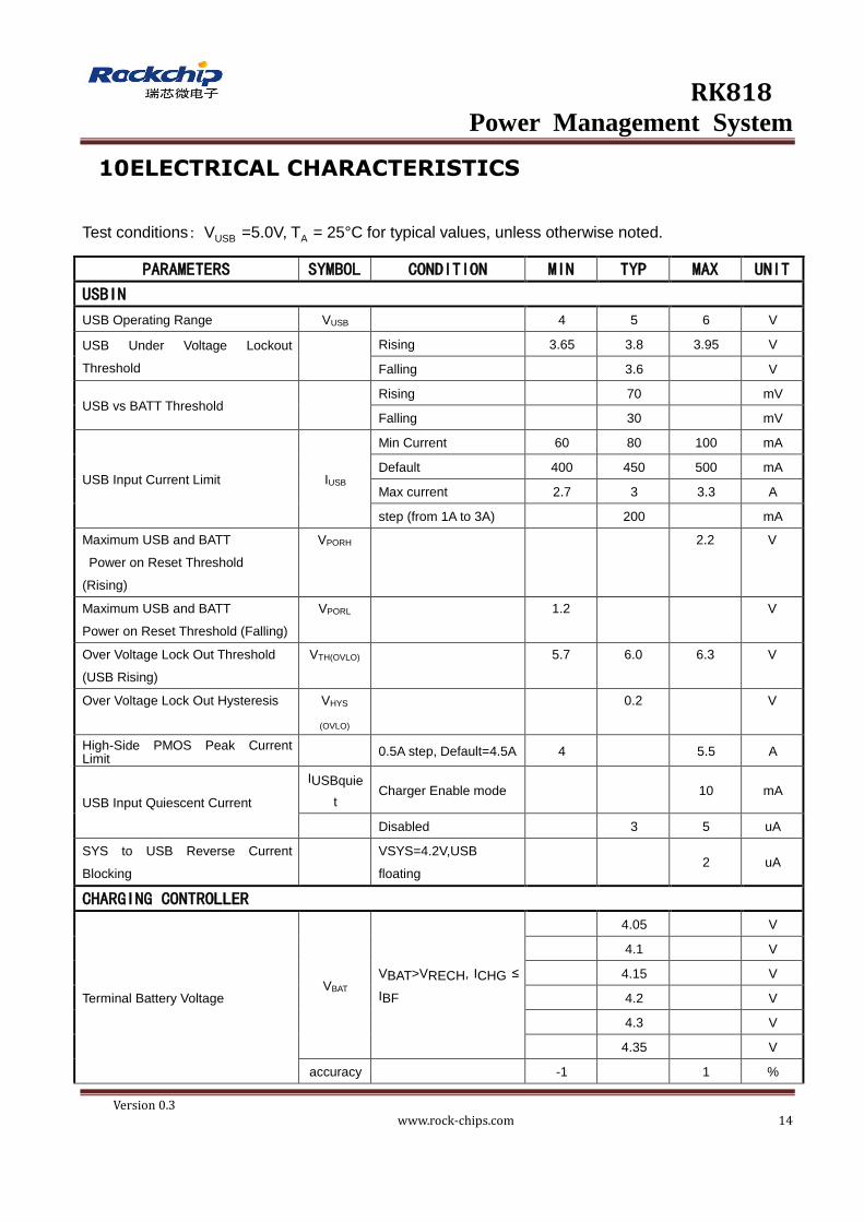
10 ELECTRICAL CHARACTERISTICS
Test conditions:VUSB =5.0V, TA = 25°C for typical values, unless otherwise noted.
PARAMETERS SYMBOL CONDITION MIN TYP MAX UNIT
USBIN
USB Operating Range VUSB 4 5 6 V
USB Under Voltage Lockout
Threshold
Rising 3.65 3.8 3.95 V
Falling 3.6 V
USB vs BATT Threshold Rising 70 mV
Falling 30 mV
USB Input Current Limit IUSB
Min Current 60 80 100 mA
Default 400 450 500 mA
Max current 2.7 3 3.3 A
step (from 1A to 3A) 200 mA
Maximum USB and BATT
Power on Reset Threshold
(Rising)
VPORH 2.2 V
Maximum USB and BATT
Power on Reset Threshold (Falling)
VPORL 1.2 V
Over Voltage Lock Out Threshold
(USB Rising)
VTH(OVLO) 5.7 6.0 6.3 V
Over Voltage Lock Out Hysteresis VHYS
(OVLO)
0.2 V
High-Side PMOS Peak Current Limit
0.5A step, Default=4.5A 4 5.5 A
USB Input Quiescent Current
IUSBquie
t Charger Enable mode 10 mA
Disabled 3 5 uA
SYS to USB Reverse Current
Blocking
VSYS=4.2V,USB
floating 2 uA
CHARGING CONTROLLER
Terminal Battery Voltage VBAT
VBAT>VRECH, ICHG ≤
IBF
4.05 V
4.1 V
4.15 V
4.2 V
4.3 V
4.35 V
accuracy -1 1 %
RK818 Power Management System
Version 0.3 www.rock-chips.com 15
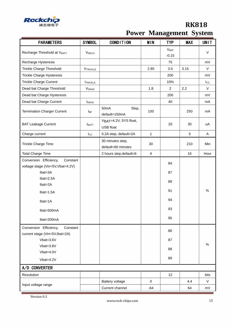
PARAMETERS SYMBOL CONDITION MIN TYP MAX UNIT
Recharge Threshold at VBATT VRECH VBAT
-0.15 V
Recharge Hysteresis 75 mV
Trickle Charge Threshold VTRICKLE 2.85 3.0 3.15 V
Trickle Charge Hysteresis 200 mV
Trickle Charge Current ITRICKLE 10% ICC
Dead bat Charge Threshold VDEAD 1.8 2 2.2 V
Dead bat Charge Hysteresis 200 mV
Dead bat Charge Current IDEAD 40 mA
Termination Charger Current IBF 50mA Step,
default=150mA 100 250 mA
BAT Leakage Current IBATT VBAT=4.2V, SYS float,
USB float 20 30 uA
Charge current ICC 0.2A step, default=2A 1 3 A
Trickle Charge Time 30 minutes step,
default=60 minutes 30 210 Min
Total Charge Time 2 hours step,default=6 4 16 Hour
Conversion Efficiency, Constant
voltage stage (Vin=5V,Vbat=4.2V)
Ibat=3A
Ibat=2.5A
Ibat=2A
Ibat=1.5A
Ibat=1A
Ibat=500mA
Ibat=200mA
84
87
89
91
94
93
95
%
Conversion Efficiency, Constant
current stage (Vin=5V,Ibat=2A)
Vbat=3.6V
Vbat=3.8V
Vbat=4.0V
Vbat=4.2V
86
87
88
89
%
A/D CONVERTER
Resolution 12 bits
Input voltage range Battery voltage 0 4.4 V
Current channel -64 64 mV
RK818 Power Management System
Version 0.3 www.rock-chips.com 16
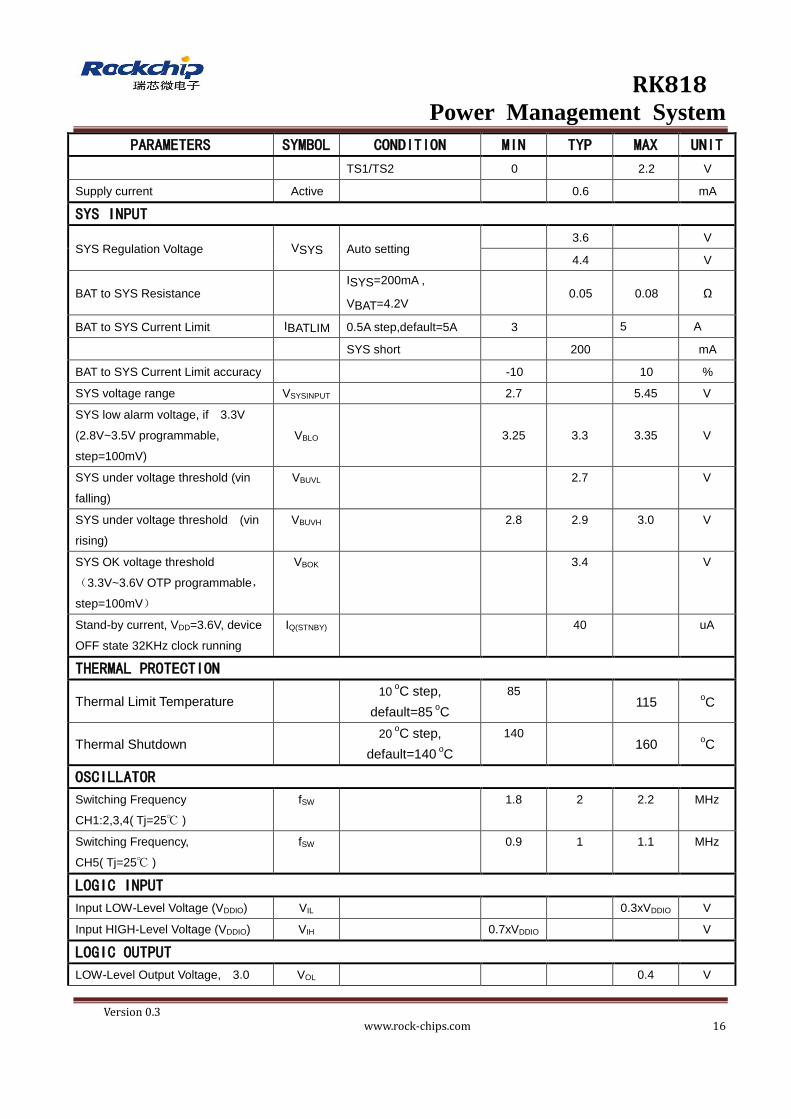
PARAMETERS SYMBOL CONDITION MIN TYP MAX UNIT
TS1/TS2 0 2.2 V
Supply current Active 0.6 mA
SYS INPUT
SYS Regulation Voltage VSYS Auto setting 3.6 V
4.4 V
BAT to SYS Resistance ISYS=200mA ,
VBAT=4.2V 0.05 0.08 Ω
BAT to SYS Current Limit IBATLIM 0.5A step,default=5A 3 5 A
SYS short 200 mA
BAT to SYS Current Limit accuracy -10 10 %
SYS voltage range VSYSINPUT 2.7 5.45 V
SYS low alarm voltage, if 3.3V
(2.8V~3.5V programmable,
step=100mV)
VBLO
3.25 3.3 3.35 V
SYS under voltage threshold (vin
falling)
VBUVL 2.7 V
SYS under voltage threshold (vin
rising)
VBUVH 2.8 2.9 3.0 V
SYS OK voltage threshold
(3.3V~3.6V OTP programmable,
step=100mV)
VBOK 3.4 V
Stand-by current, VDD=3.6V, device
OFF state 32KHz clock running
IQ(STNBY) 40 uA
THERMAL PROTECTION
Thermal Limit Temperature 10
oC step,
default=85 oC
85 115
oC
Thermal Shutdown 20
oC step,
default=140 oC
140 160
oC
OSCILLATOR
Switching Frequency
CH1:2,3,4( Tj=25 )
fSW 1.8 2 2.2 MHz
Switching Frequency,
CH5( Tj=25 )
fSW 0.9 1 1.1 MHz
LOGIC INPUT
Input LOW-Level Voltage (VDDIO) VIL 0.3xVDDIO V
Input HIGH-Level Voltage (VDDIO) VIH 0.7xVDDIO V
LOGIC OUTPUT
LOW-Level Output Voltage, 3.0 VOL 0.4 V
RK818 Power Management System
Version 0.3 www.rock-chips.com 17
PARAMETERS SYMBOL CONDITION MIN TYP MAX UNIT
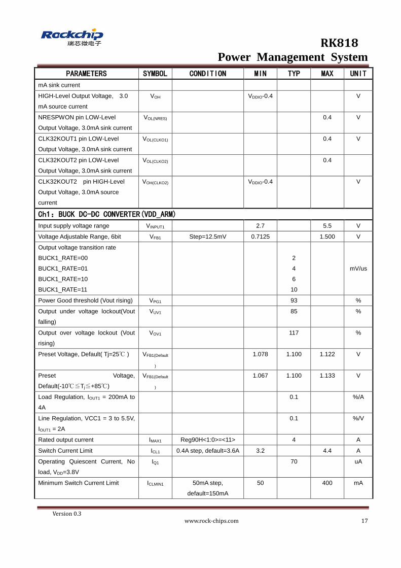
mA sink current
HIGH-Level Output Voltage, 3.0
mA source current
VOH VDDIO-0.4 V
NRESPWON pin LOW-Level
Output Voltage, 3.0mA sink current
VOL(NRES) 0.4 V
CLK32KOUT1 pin LOW-Level
Output Voltage, 3.0mA sink current
VOL(CLKO1) 0.4 V
CLK32KOUT2 pin LOW-Level
Output Voltage, 3.0mA sink current
VOL(CLKO2) 0.4
CLK32KOUT2 pin HIGH-Level
Output Voltage, 3.0mA source
current
VOH(CLKO2) VDDIO-0.4 V
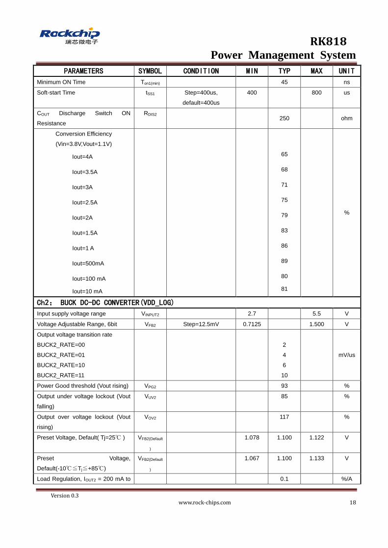
Ch1:BUCK DC-DC CONVERTER(VDD_ARM)
Input supply voltage range VINPUT1 2.7 5.5 V
Voltage Adjustable Range, 6bit VFB1 Step=12.5mV 0.7125 1.500 V
Output voltage transition rate
BUCK1_RATE=00
BUCK1_RATE=01
BUCK1_RATE=10
BUCK1_RATE=11
2
4
6
10
mV/us
Power Good threshold (Vout rising) VPG1 93 %
Output under voltage lockout(Vout
falling)
VUV1 85 %
Output over voltage lockout (Vout
rising)
VOV1 117 %
Preset Voltage, Default( Tj=25 ) VFB1(Default
)
1.078 1.100 1.122 V
Preset Voltage,
Default(-10≦Tj≦+85)
VFB1(Default
)
1.067 1.100 1.133 V
Load Regulation, IOUT1 = 200mA to
4A
0.1 %/A
Line Regulation, VCC1 = 3 to 5.5V,
IOUT1 = 2A
0.1 %/V
Rated output current IMAX1 Reg90H<1:0>=<11> 4 A
Switch Current Limit ICL1 0.4A step, default=3.6A 3.2 4.4 A
Operating Quiescent Current, No
load, VDD=3.8V
IQ1 70 uA
Minimum Switch Current Limit
ICLMIN1 50mA step,
default=150mA
50 400 mA
RK818 Power Management System
Version 0.3 www.rock-chips.com 18
PARAMETERS SYMBOL CONDITION MIN TYP MAX UNIT
Minimum ON Time Ton1(min) 45 ns
Soft-start Time tSS1 Step=400us,
default=400us
400 800 us
COUT Discharge Switch ON
Resistance
RDIS2 250 ohm
Conversion Efficiency
(Vin=3.8V,Vout=1.1V)
Iout=4A
Iout=3.5A
Iout=3A
Iout=2.5A
Iout=2A
Iout=1.5A
Iout=1 A
Iout=500mA
Iout=100 mA
Iout=10 mA
65
68
71
75
79
83
86
89
80
81
%
Ch2: BUCK DC-DC CONVERTER(VDD_LOG)
Input supply voltage range VINPUT2 2.7 5.5 V
Voltage Adjustable Range, 6bit VFB2 Step=12.5mV 0.7125 1.500 V
Output voltage transition rate
BUCK2_RATE=00
BUCK2_RATE=01
BUCK2_RATE=10
BUCK2_RATE=11
2
4
6
10
mV/us
Power Good threshold (Vout rising) VPG2 93 %
Output under voltage lockout (Vout
falling)
VUV2 85 %
Output over voltage lockout (Vout
rising)
VOV2 117 %
Preset Voltage, Default( Tj=25 ) VFB2(Default
)
1.078 1.100 1.122 V
Preset Voltage,
Default(-10≦Tj≦+85)
VFB2(Default
)
1.067 1.100 1.133 V
Load Regulation, IOUT2 = 200 mA to 0.1 %/A
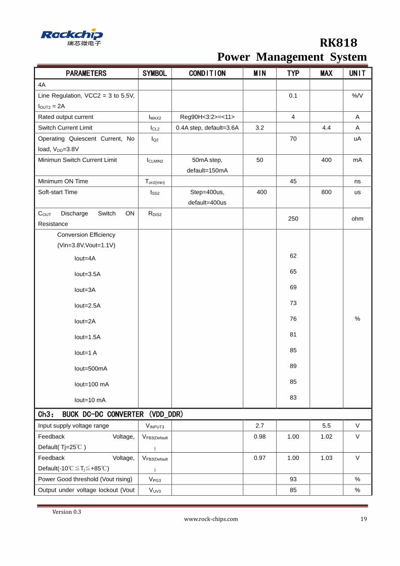
RK818 Power Management System
Version 0.3 www.rock-chips.com 19
PARAMETERS SYMBOL CONDITION MIN TYP MAX UNIT
4A
Line Regulation, VCC2 = 3 to 5.5V,
IOUT2 = 2A
0.1 %/V
Rated output current IMAX2 Reg90H<3:2>=<11> 4 A
Switch Current Limit ICL2 0.4A step, default=3.6A 3.2 4.4 A
Operating Quiescent Current, No
load, VDD=3.8V
IQ2 70 uA
Minimun Switch Current Limit
ICLMIN2 50mA step,
default=150mA
50 400 mA
Minimum ON Time Ton2(min) 45 ns
Soft-start Time tSS2 Step=400us,
default=400us
400 800 us
COUT Discharge Switch ON
Resistance
RDIS2 250 ohm
Conversion Efficiency
(Vin=3.8V,Vout=1.1V)
Iout=4A
Iout=3.5A
Iout=3A
Iout=2.5A
Iout=2A
Iout=1.5A
Iout=1 A
Iout=500mA
Iout=100 mA
Iout=10 mA
62
65
69
73
76
81
85
89
85
83
%
Ch3: BUCK DC-DC CONVERTER (VDD_DDR)
Input supply voltage range VINPUT3 2.7 5.5 V
Feedback Voltage,
Default( Tj=25 )
VFB3(Default
)
0.98 1.00 1.02 V
Feedback Voltage,
Default(-10≦Tj≦+85)
VFB3(Default
)
0.97 1.00 1.03 V
Power Good threshold (Vout rising) VPG3 93 %
Output under voltage lockout (Vout VUV3 85 %
RK818 Power Management System
Version 0.3 www.rock-chips.com 20
PARAMETERS SYMBOL CONDITION MIN TYP MAX UNIT
falling)
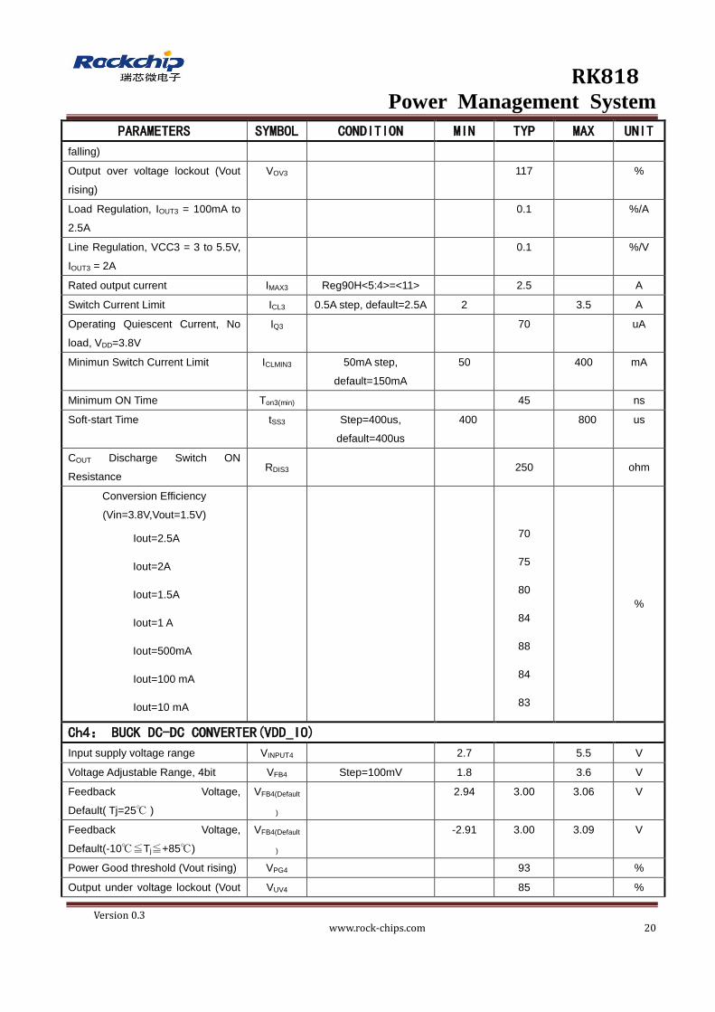
Output over voltage lockout (Vout
rising)
VOV3 117 %
Load Regulation, IOUT3 = 100mA to
2.5A
0.1 %/A
Line Regulation, VCC3 = 3 to 5.5V,
IOUT3 = 2A
0.1 %/V
Rated output current IMAX3 Reg90H<5:4>=<11> 2.5 A
Switch Current Limit ICL3 0.5A step, default=2.5A 2 3.5 A
Operating Quiescent Current, No
load, VDD=3.8V
IQ3 70 uA
Minimun Switch Current Limit
ICLMIN3 50mA step,
default=150mA
50 400 mA
Minimum ON Time Ton3(min) 45 ns
Soft-start Time tSS3 Step=400us,
default=400us
400 800 us
COUT Discharge Switch ON
Resistance RDIS3
250 ohm
Conversion Efficiency
(Vin=3.8V,Vout=1.5V)
Iout=2.5A
Iout=2A
Iout=1.5A
Iout=1 A
Iout=500mA
Iout=100 mA
Iout=10 mA
70
75
80
84
88
84
83
%
Ch4: BUCK DC-DC CONVERTER(VDD_IO)
Input supply voltage range VINPUT4 2.7 5.5 V
Voltage Adjustable Range, 4bit VFB4 Step=100mV 1.8 3.6 V
Feedback Voltage,
Default( Tj=25 )
VFB4(Default
)
2.94 3.00 3.06 V
Feedback Voltage,
Default(-10≦Tj≦+85)
VFB4(Default
)
-2.91 3.00 3.09 V
Power Good threshold (Vout rising) VPG4 93 %
Output under voltage lockout (Vout VUV4 85 %
RK818 Power Management System
Version 0.3 www.rock-chips.com 21
PARAMETERS SYMBOL CONDITION MIN TYP MAX UNIT
falling)
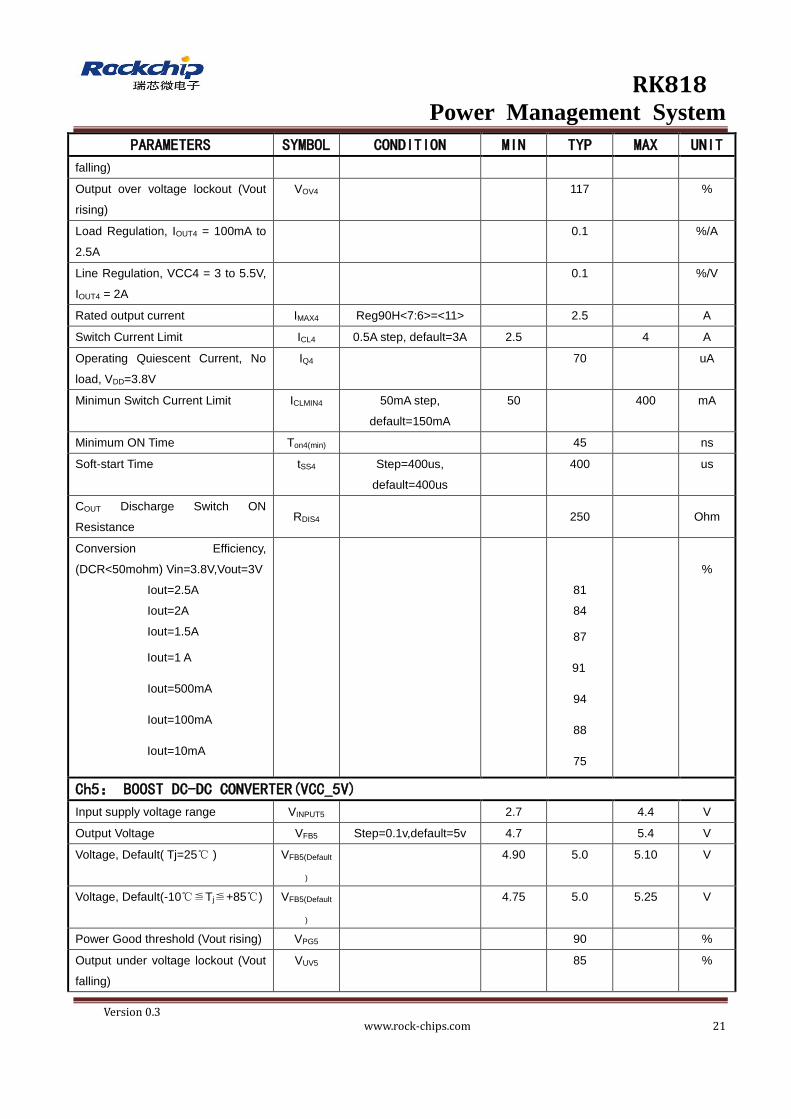
Output over voltage lockout (Vout
rising)
VOV4 117 %
Load Regulation, IOUT4 = 100mA to
2.5A
0.1 %/A
Line Regulation, VCC4 = 3 to 5.5V,
IOUT4 = 2A
0.1 %/V
Rated output current IMAX4 Reg90H<7:6>=<11> 2.5 A
Switch Current Limit ICL4 0.5A step, default=3A 2.5 4 A
Operating Quiescent Current, No
load, VDD=3.8V
IQ4 70 uA
Minimun Switch Current Limit
ICLMIN4 50mA step,
default=150mA
50 400 mA
Minimum ON Time Ton4(min) 45 ns
Soft-start Time tSS4 Step=400us,
default=400us
400 us
COUT Discharge Switch ON
Resistance RDIS4
250 Ohm
Conversion Efficiency,
(DCR<50mohm) Vin=3.8V,Vout=3V
Iout=2.5A
Iout=2A
Iout=1.5A
Iout=1 A
Iout=500mA
Iout=100mA
Iout=10mA
81
84
87
91
94
88
75
%
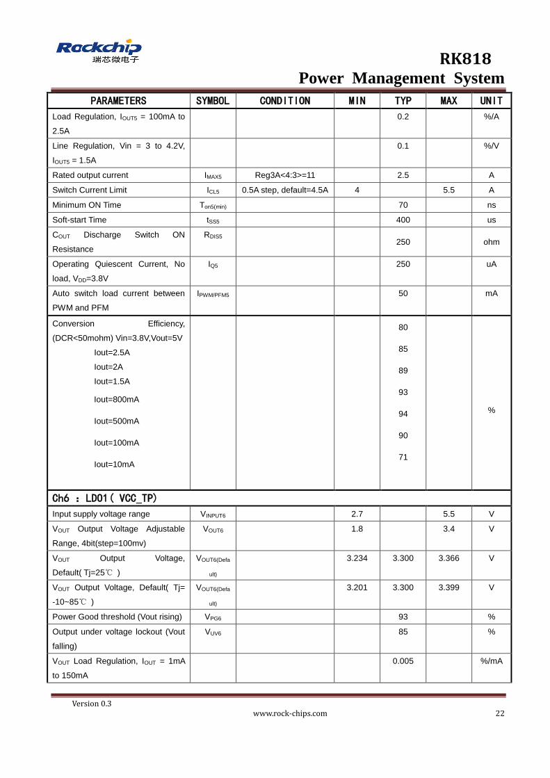
Ch5: BOOST DC-DC CONVERTER(VCC_5V)
Input supply voltage range VINPUT5 2.7 4.4 V
Output Voltage VFB5 Step=0.1v,default=5v 4.7 5.4 V
Voltage, Default( Tj=25 ) VFB5(Default
)
4.90 5.0 5.10 V
Voltage, Default(-10≦Tj≦+85) VFB5(Default
)
4.75 5.0 5.25 V
Power Good threshold (Vout rising) VPG5 90 %
Output under voltage lockout (Vout
falling)
VUV5 85 %
RK818 Power Management System
Version 0.3 www.rock-chips.com 22
PARAMETERS SYMBOL CONDITION MIN TYP MAX UNIT
Load Regulation, IOUT5 = 100mA to
2.5A
0.2 %/A
Line Regulation, Vin = 3 to 4.2V,
IOUT5 = 1.5A
0.1 %/V
Rated output current IMAX5 Reg3A<4:3>=11 2.5 A
Switch Current Limit ICL5 0.5A step, default=4.5A 4 5.5 A
Minimum ON Time Ton5(min) 70 ns
Soft-start Time tSS5 400 us
COUT Discharge Switch ON
Resistance
RDIS5 250 ohm
Operating Quiescent Current, No
load, VDD=3.8V
IQ5 250 uA
Auto switch load current between
PWM and PFM
IPWM/PFM5 50 mA
Conversion Efficiency,
(DCR<50mohm) Vin=3.8V,Vout=5V
Iout=2.5A
Iout=2A
Iout=1.5A
Iout=800mA
Iout=500mA
Iout=100mA
Iout=10mA
80
85
89
93
94
90
71
%
Ch6 :LDO1( VCC_TP)
Input supply voltage range VINPUT6 2.7 5.5 V
VOUT Output Voltage Adjustable
Range, 4bit(step=100mv)
VOUT6 1.8 3.4 V
VOUT Output Voltage,
Default( Tj=25 )
VOUT6(Defa
ult)
3.234 3.300 3.366 V
VOUT Output Voltage, Default( Tj=
-10~85 )
VOUT6(Defa
ult)
3.201 3.300 3.399 V
Power Good threshold (Vout rising) VPG6 93 %
Output under voltage lockout (Vout
falling)
VUV6 85 %
VOUT Load Regulation, IOUT = 1mA
to 150mA
0.005 %/mA
RK818 Power Management System
Version 0.3 www.rock-chips.com 23
PARAMETERS SYMBOL CONDITION MIN TYP MAX UNIT
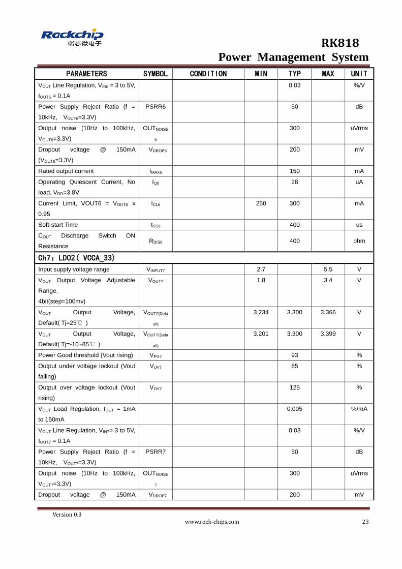
VOUT Line Regulation, VIN6 = 3 to 5V,
IOUT6 = 0.1A
0.03 %/V
Power Supply Reject Ratio (f =
10kHz, VOUT6=3.3V)
PSRR6 50 dB
Output noise (10Hz to 100kHz,
VOUT6=3.3V)
OUTNOISE
6
300 uVrms
Dropout voltage @ 150mA
(VOUT6=3.3V)
VDROP6 200 mV
Rated output current IMAX6 150 mA
Operating Quiescent Current, No
load, VDD=3.8V
IQ6 28 uA
Current Limit, VOUT6 = VOUT6 x
0.95
ICL6 250 300 mA
Soft-start Time tSS6 400 us
COUT Discharge Switch ON
Resistance RDIS6
400 ohm
Ch7:LDO2( VCCA_33)
Input supply voltage range VINPUT7 2.7 5.5 V
VOUT Output Voltage Adjustable
Range,
4bit(step=100mv)
VOUT7 1.8 3.4 V
VOUT Output Voltage,
Default( Tj=25 )
VOUT7(Defa
ult)
3.234 3.300 3.366 V
VOUT Output Voltage,
Default( Tj=-10~85 )
VOUT7(Defa
ult)
3.201 3.300 3.399 V
Power Good threshold (Vout rising) VPG7 93 %
Output under voltage lockout (Vout
falling)
VUV7 85 %
Output over voltage lockout (Vout
rising)
VOV7 125 %
VOUT Load Regulation, IOUT = 1mA
to 150mA
0.005 %/mA
VOUT Line Regulation, VIN7= 3 to 5V,
IOUT7 = 0.1A
0.03 %/V
Power Supply Reject Ratio (f =
10kHz, VOUT7=3.3V)
PSRR7 50 dB
Output noise (10Hz to 100kHz,
VOUT7=3.3V)
OUTNOISE
7
300 uVrms
Dropout voltage @ 150mA VDROP7 200 mV
RK818 Power Management System
Version 0.3 www.rock-chips.com 24
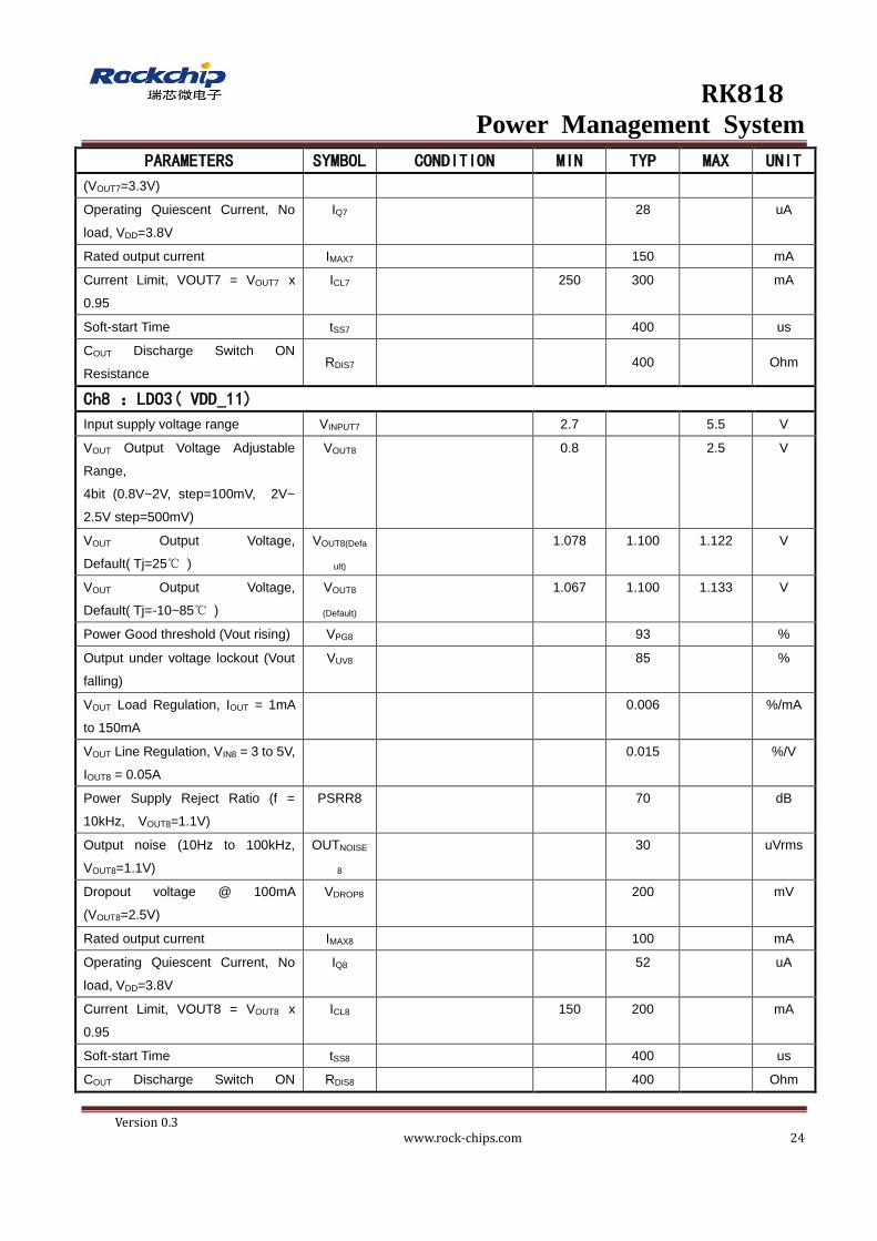
PARAMETERS SYMBOL CONDITION MIN TYP MAX UNIT
(VOUT7=3.3V)
Operating Quiescent Current, No
load, VDD=3.8V
IQ7 28 uA
Rated output current IMAX7 150 mA
Current Limit, VOUT7 = VOUT7 x
0.95
ICL7 250 300 mA
Soft-start Time tSS7 400 us
COUT Discharge Switch ON
Resistance RDIS7
400 Ohm
Ch8 :LDO3( VDD_11)
Input supply voltage range VINPUT7 2.7 5.5 V
VOUT Output Voltage Adjustable
Range,
4bit (0.8V~2V, step=100mV, 2V~
2.5V step=500mV)
VOUT8 0.8 2.5 V
VOUT Output Voltage,
Default( Tj=25 )
VOUT8(Defa
ult)
1.078 1.100 1.122 V
VOUT Output Voltage,
Default( Tj=-10~85 )
VOUT8
(Default)
1.067 1.100 1.133 V
Power Good threshold (Vout rising) VPG8 93 %
Output under voltage lockout (Vout
falling)
VUV8 85 %
VOUT Load Regulation, IOUT = 1mA
to 150mA
0.006 %/mA
VOUT Line Regulation, VIN8 = 3 to 5V,
IOUT8 = 0.05A
0.015 %/V
Power Supply Reject Ratio (f =
10kHz, VOUT8=1.1V)
PSRR8 70 dB
Output noise (10Hz to 100kHz,
VOUT8=1.1V)
OUTNOISE
8
30 uVrms
Dropout voltage @ 100mA
(VOUT8=2.5V)
VDROP8 200 mV
Rated output current IMAX8 100 mA
Operating Quiescent Current, No
load, VDD=3.8V
IQ8 52 uA
Current Limit, VOUT8 = VOUT8 x
0.95
ICL8 150 200 mA
Soft-start Time tSS8 400 us
COUT Discharge Switch ON RDIS8 400 Ohm
RK818 Power Management System
Version 0.3 www.rock-chips.com 25
PARAMETERS SYMBOL CONDITION MIN TYP MAX UNIT
Resistance
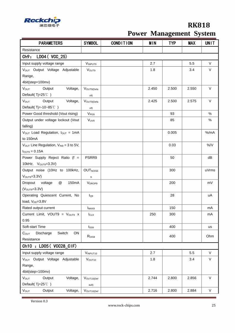
Ch9: LDO4( VCC_25)
Input supply voltage range VINPUT9 2.7 5.5 V
VOUT Output Voltage Adjustable
Range,
4bit(step=100mv)
VOUT9 1.8 3.4 V
VOUT Output Voltage,
Default( Tj=25 )
VOUT9(Defa
ult)
2.450 2.500 2.550 V
VOUT Output Voltage,
Default( Tj=-10~85 )
VOUT9(Defa
ult)
2.425 2.500 2.575 V
Power Good threshold (Vout rising) VPG9 93 %
Output under voltage lockout (Vout
falling)
VUV9 85 %
VOUT Load Regulation, IOUT = 1mA
to 150mA
0.005 %/mA
VOUT Line Regulation, VIN9 = 3 to 5V,
IOUT9 = 0.15A
0.03 %/V
Power Supply Reject Ratio (f =
10kHz, VOUT9=3.3V)
PSRR9 50 dB
Output noise (10Hz to 100kHz,
VOUT9=3.3V)
OUTNOISE
9
300 uVrms
Dropout voltage @ 150mA
(VOUT9=3.3V)
VDROP9 200 mV
Operating Quiescent Current, No
load, VDD=3.8V
IQ9 28 uA
Rated output current IMAX9 150 mA
Current Limit, VOUT9 = VOUT9 x
0.95
ICL9 250 300 mA
Soft-start Time tSS9 400 us
COUT Discharge Switch ON
Resistance RDIS9
400 Ohm
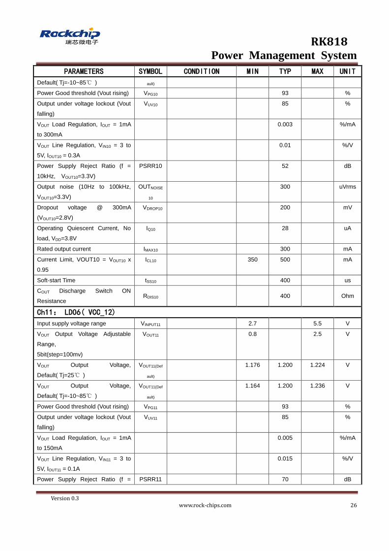
Ch10 :LDO5( VCC28_CIF)
Input supply voltage range VINPUT10 2.7 5.5 V
VOUT Output Voltage Adjustable
Range,
4bit(step=100mv)
VOUT10 1.8 3.4 V
VOUT Output Voltage,
Default( Tj=25 )
VOUT10(Def
ault)
2.744 2.800 2.856 V
VOUT Output Voltage, VOUT10(Def 2.716 2.800 2.884 V
RK818 Power Management System
Version 0.3 www.rock-chips.com 26
PARAMETERS SYMBOL CONDITION MIN TYP MAX UNIT
Default( Tj=-10~85 ) ault)
Power Good threshold (Vout rising) VPG10 93 %
Output under voltage lockout (Vout
falling)
VUV10 85 %
VOUT Load Regulation, IOUT = 1mA
to 300mA
0.003 %/mA
VOUT Line Regulation, VIN10 = 3 to
5V, IOUT10 = 0.3A
0.01 %/V
Power Supply Reject Ratio (f =
10kHz, VOUT10=3.3V)
PSRR10 52 dB
Output noise (10Hz to 100kHz,
VOUT10=3.3V)
OUTNOISE
10
300 uVrms
Dropout voltage @ 300mA
(VOUT10=2.8V)
VDROP10 200 mV
Operating Quiescent Current, No
load, VDD=3.8V
IQ10 28 uA
Rated output current IMAX10 300 mA
Current Limit, VOUT10 = VOUT10 x
0.95
ICL10 350 500 mA
Soft-start Time tSS10 400 us
COUT Discharge Switch ON
Resistance RDIS10
400 Ohm
Ch11: LDO6( VCC_12)
Input supply voltage range VINPUT11 2.7 5.5 V
VOUT Output Voltage Adjustable
Range,
5bit(step=100mv)
VOUT11 0.8 2.5 V
VOUT Output Voltage,
Default( Tj=25 )
VOUT11(Def
ault)
1.176 1.200 1.224 V
VOUT Output Voltage,
Default( Tj=-10~85 )
VOUT11(Def
ault)
1.164 1.200 1.236 V
Power Good threshold (Vout rising) VPG11 93 %
Output under voltage lockout (Vout
falling)
VUV11 85 %
VOUT Load Regulation, IOUT = 1mA
to 150mA
0.005 %/mA
VOUT Line Regulation, VIN11 = 3 to
5V, IOUT11 = 0.1A
0.015 %/V
Power Supply Reject Ratio (f = PSRR11 70 dB
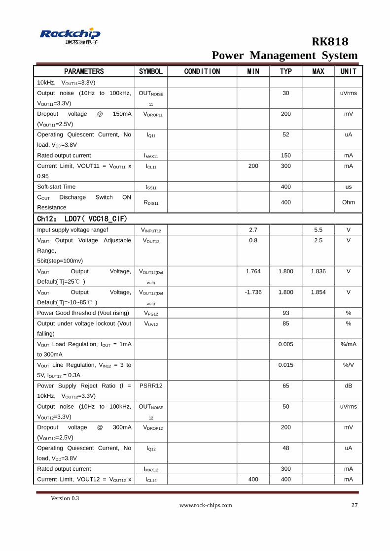
RK818 Power Management System
Version 0.3 www.rock-chips.com 27
PARAMETERS SYMBOL CONDITION MIN TYP MAX UNIT
10kHz, VOUT11=3.3V)
Output noise (10Hz to 100kHz,
VOUT11=3.3V)
OUTNOISE
11
30 uVrms
Dropout voltage @ 150mA
(VOUT11=2.5V)
VDROP11 200 mV
Operating Quiescent Current, No
load, VDD=3.8V
IQ11 52 uA
Rated output current IMAX11 150 mA
Current Limit, VOUT11 = VOUT11 x
0.95
ICL11 200 300 mA
Soft-start Time tSS11 400 us
COUT Discharge Switch ON
Resistance RDIS11
400 Ohm
Ch12: LDO7( VCC18_CIF)
Input supply voltage rangef VINPUT12 2.7 5.5 V
VOUT Output Voltage Adjustable
Range,
5bit(step=100mv)
VOUT12 0.8 2.5 V
VOUT Output Voltage,
Default( Tj=25 )
VOUT12(Def
ault)
1.764 1.800 1.836 V
VOUT Output Voltage,
Default( Tj=-10~85 )
VOUT12(Def
ault)
-1.736 1.800 1.854 V
Power Good threshold (Vout rising) VPG12 93 %
Output under voltage lockout (Vout
falling)
VUV12 85 %
VOUT Load Regulation, IOUT = 1mA
to 300mA
0.005 %/mA
VOUT Line Regulation, VIN12 = 3 to
5V, IOUT12 = 0.3A
0.015 %/V
Power Supply Reject Ratio (f =
10kHz, VOUT12=3.3V)
PSRR12 65 dB
Output noise (10Hz to 100kHz,
VOUT12=3.3V)
OUTNOISE
12
50 uVrms
Dropout voltage @ 300mA
(VOUT12=2.5V)
VDROP12 200 mV
Operating Quiescent Current, No
load, VDD=3.8V
IQ12 48 uA
Rated output current IMAX12 300 mA
Current Limit, VOUT12 = VOUT12 x ICL12 400 400 mA
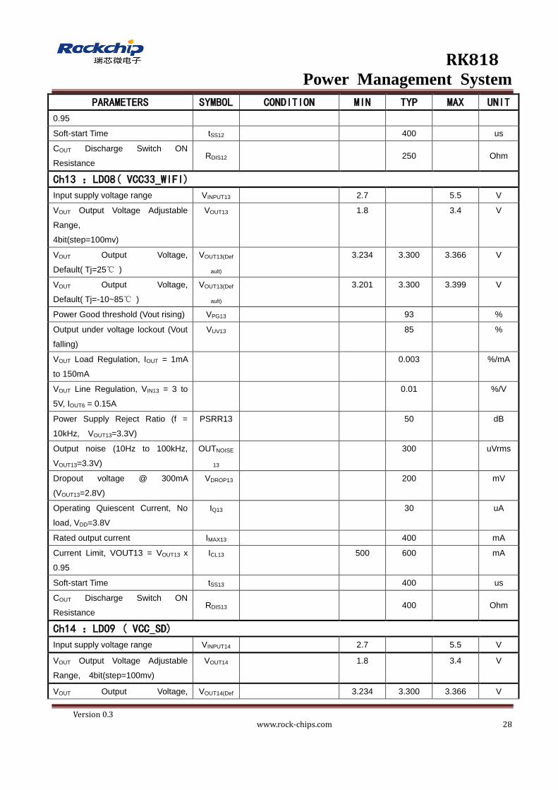
RK818 Power Management System
Version 0.3 www.rock-chips.com 28
PARAMETERS SYMBOL CONDITION MIN TYP MAX UNIT
0.95
Soft-start Time tSS12 400 us
COUT Discharge Switch ON
Resistance RDIS12
250 Ohm
Ch13 :LDO8( VCC33_WIFI)
Input supply voltage range VINPUT13 2.7 5.5 V
VOUT Output Voltage Adjustable
Range,
4bit(step=100mv)
VOUT13 1.8 3.4 V
VOUT Output Voltage,
Default( Tj=25 )
VOUT13(Def
ault)
3.234 3.300 3.366 V
VOUT Output Voltage,
Default( Tj=-10~85 )
VOUT13(Def
ault)
3.201 3.300 3.399 V
Power Good threshold (Vout rising) VPG13 93 %
Output under voltage lockout (Vout
falling)
VUV13 85 %
VOUT Load Regulation, IOUT = 1mA
to 150mA
0.003 %/mA
VOUT Line Regulation, VIN13 = 3 to
5V, IOUT6 = 0.15A
0.01 %/V
Power Supply Reject Ratio (f =
10kHz, VOUT13=3.3V)
PSRR13 50 dB
Output noise (10Hz to 100kHz,
VOUT13=3.3V)
OUTNOISE
13
300 uVrms
Dropout voltage @ 300mA
(VOUT13=2.8V)
VDROP13 200 mV
Operating Quiescent Current, No
load, VDD=3.8V
IQ13 30 uA
Rated output current IMAX13 400 mA
Current Limit, VOUT13 = VOUT13 x
0.95
ICL13 500 600 mA
Soft-start Time tSS13 400 us
COUT Discharge Switch ON
Resistance RDIS13
400 Ohm
Ch14 :LDO9 ( VCC_SD)
Input supply voltage range VINPUT14 2.7 5.5 V
VOUT Output Voltage Adjustable
Range, 4bit(step=100mv)
VOUT14 1.8 3.4 V
VOUT Output Voltage, VOUT14(Def 3.234 3.300 3.366 V
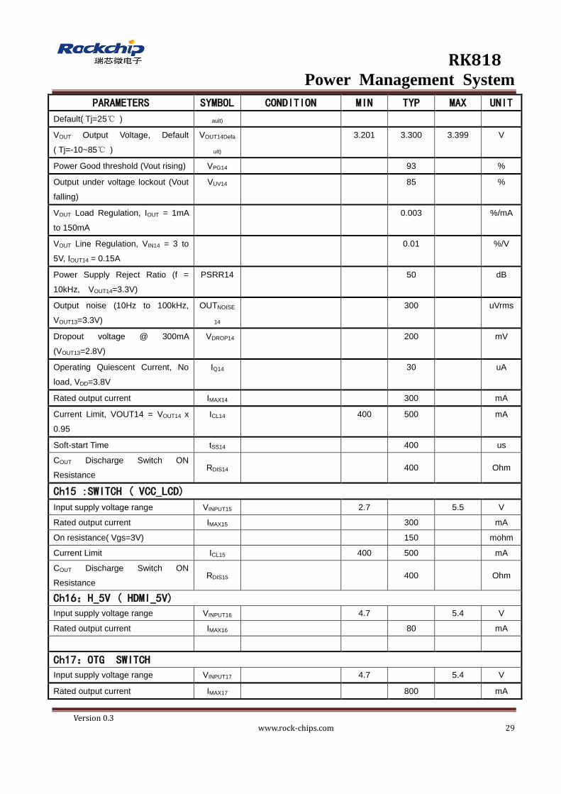
RK818 Power Management System
Version 0.3 www.rock-chips.com 29
PARAMETERS SYMBOL CONDITION MIN TYP MAX UNIT
Default( Tj=25 ) ault)
VOUT Output Voltage, Default
( Tj=-10~85 )
VOUT14Defa
ult)
3.201 3.300 3.399 V
Power Good threshold (Vout rising) VPG14 93 %
Output under voltage lockout (Vout
falling)
VUV14 85 %
VOUT Load Regulation, IOUT = 1mA
to 150mA
0.003 %/mA
VOUT Line Regulation, VIN14 = 3 to
5V, IOUT14 = 0.15A
0.01 %/V
Power Supply Reject Ratio (f =
10kHz, VOUT14=3.3V)
PSRR14 50 dB
Output noise (10Hz to 100kHz,
VOUT13=3.3V)
OUTNOISE
14
300 uVrms
Dropout voltage @ 300mA
(VOUT13=2.8V)
VDROP14 200 mV
Operating Quiescent Current, No
load, VDD=3.8V
IQ14 30 uA
Rated output current IMAX14 300 mA
Current Limit, VOUT14 = VOUT14 x
0.95
ICL14 400 500 mA
Soft-start Time tSS14 400 us
COUT Discharge Switch ON
Resistance RDIS14
400 Ohm
Ch15 :SWITCH ( VCC_LCD)
Input supply voltage range VINPUT15 2.7 5.5 V
Rated output current IMAX15 300 mA
On resistance( Vgs=3V) 150 mohm
Current Limit ICL15 400 500 mA
COUT Discharge Switch ON
Resistance RDIS15
400 Ohm
Ch16:H_5V ( HDMI_5V) Input supply voltage range VINPUT16 4.7 5.4 V
Rated output current IMAX16 80 mA
Ch17:OTG SWITCH
Input supply voltage range VINPUT17 4.7 5.4 V
Rated output current IMAX17 800 mA
RK818 Power Management System
Version 0.3 www.rock-chips.com 30
PARAMETERS SYMBOL CONDITION MIN TYP MAX UNIT
output current limit ICL17 0.1A step, default=0.8A 0.7 1 A
RTC
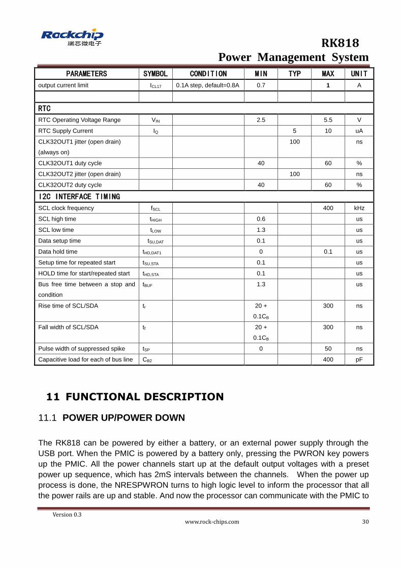
RTC Operating Voltage Range VIN 2.5 5.5 V
RTC Supply Current IQ 5 10 uA
CLK32OUT1 jitter (open drain)
(always on)
100 ns
CLK32OUT1 duty cycle 40 60 %
CLK32OUT2 jitter (open drain) 100 ns
CLK32OUT2 duty cycle 40 60 %
I2C INTERFACE TIMING
SCL clock frequency fSCL 400 kHz
SCL high time tHIGH 0.6 us
SCL low time tLOW 1.3 us
Data setup time tSU,DAT 0.1 us
Data hold time tHD,DAT1 0 0.1 us
Setup time for repeated start tSU,STA 0.1 us
HOLD time for start/repeated start tHD,STA 0.1 us
Bus free time between a stop and
condition
tBUF 1.3 us
Rise time of SCL/SDA tr 20 +
0.1CB
300 ns
Fall width of SCL/SDA tf 20 +
0.1CB
300 ns
Pulse width of suppressed spike tSP 0 50 ns
Capacitive load for each of bus line CB2 400 pF
11 FUNCTIONAL DESCRIPTION
POWER UP/POWER DOWN 11.1
The RK818 can be powered by either a battery, or an external power supply through the
USB port. When the PMIC is powered by a battery only, pressing the PWRON key powers
up the PMIC. All the power channels start up at the default output voltages with a preset
power up sequence, which has 2mS intervals between the channels. When the power up
process is done, the NRESPWRON turns to high logic level to inform the processor that all
the power rails are up and stable. And now the processor can communicate with the PMIC to
RK818 Power Management System
Version 0.3 www.rock-chips.com 31
re-configure the output voltage of each power channel if needed.
To power down the PMIC, the processor needs to issue a “power down” signal through the
I2C interface. Upon receiving the power down signal, the PMIC first saves all the information
on the existing states, and then switches the NRESPWRON to low logic level. At this point,
the power channels start to be turned off one after another with the power down sequence. If
for any reason the processor fails to issue the power down signal, the PMIC can be powered
off by “pressing and holding” the PWRON key.
In a case where a battery is the sole power supply and the PMIC is in off state, when an
external power supply is plugged into the USB, the PMIC will first check to see if this is a
valid power supply. If the power supply from the USB is valid, then the power channels are
turned on and the battery is charged.
SWITCHING CHARGER 11.2
The RK818 has integrated a switch mode charger, which provides the functions like trickle
current charging, constant current charging, constant voltage charging, charging termination,
automatic recharging, battery temperature monitoring, charging timer and thermal feedback
protection. The values of constant current and constant voltage charging can be set through
I2C interface.
The input average current limit function allows as large as possible a charging current to be
used without having to worry about the input current exceeding the maximum current
allowed by the USB port. The input current limits can be configured through I2C interface. For
example, when an USB port is used as the input, the input current limit can be configured to
either 450mA, or 820mA, to meet the requirements of USB2.0 and USB3.0: respectively.
The charger also has a timer function which sets the maximum charging time for trickle,
constant current and constant voltage charging, respectively. If the charging does not
complete when a preset maximum charging time is reached, the charging is terminated.
The battery temperature can be monitored through the TS1 pin. A battery typically has a
thermistor inside. The RK818 sinks a constant current into the thermistor and senses the
voltage across the thermistor through an internal ADC. A safe charging temperature range is
preset in the PMIC. The charging can proceed normally if the battery temperature falls within
the preset range. If, however, the battery temperature goes either above the upper limit or
below the lower limit of the preset range, the charging will pause until the battery
temperature goes back in the preset range. If the value of the available thermistor is either
too large or too small, a normal resistor can be connected in series or in parallel with the
thermistor so that the sensed voltage fits the ADC’s input range.
RK818 Power Management System
Version 0.3 www.rock-chips.com 32
During Charging, Vsys will be set to 3.6V when the battery voltage is below 3.6V. This design
is to guarantee that when an external power supply is plugged into the USB port to charge
the battery while the battery voltage is low, the Vsys is already at 3.6V, which allows the
PMIC to start up quickly without having to wait for the Vsys ramping up.
POWER PATH MANAGEMENT 11.3
A power path management function is integrated in the RK818, which, together with the
accurate input current limit function, can provide intelligent power path control. In a power
path control process, the PMIC gives the outputs, or the system loads, the highest priority of
using the input power. The battery is getting charged only if the input power is greater than
the output power required by the system loads. The intelligent power path control function
automatically reduces the charging current when the output power required by the loads
increases. In an extreme case where the required output power is greater than the input
power, the charging current will be cut off and the battery will join the input power supply to
provide power to the load. This is how the intelligent power path control works: As the system
power loading increases, the PMIC will draw more input current from the power supply to
meet the output power requirement while keep the charging current unchanged. If the
system power loading continues to increase to the point where the input current limit is
reached, then the PMIC will lower the charging current so that enough power still goes to the
load. If the system power loading further increases and due to the input current limit, the
input power can not meet the output power requirement, then the battery will start to
discharge to supply power to the load together with the USB power supply. If for some
reason the USB is unplugged, the battery will automatically switched in to take over the USB
power supply and provide full power to the load. The wide power path loop bandwidth allows
all the above mentioned power path switching transient to be quick and seamless and
therefore no overshoot and notch occur at the system and output voltages.
To minimize the loss from the voltage drop along the current path when the battery is
charged or discharged, a 50mΩ MOSFET is integrated in the RK818 to serve as a control
switch as well as the power switch of the switching mode battery charger.
THERMAL FOLDBACK 11.4
Generally speaking, the higher the operating junction temperature is, the shorter the chip’s
life time. Therefore, keeping the operating junction temperature as low as possible is one of
the keys in reliability design. The RK818 provides a thermal feedback protection function for
RK818 Power Management System
Version 0.3 www.rock-chips.com 33
charging process. When the die temperature reaches a preset value, the PMIC will lower the
charging current so as to keep the die temperature within an appropriate range. The life time
of the PMIC equipped with this function can be reliably prolonged and no over-heat damage
will occur.
BATTERY FUEL GAUGE 11.5
The RK818 provides an accurate battery fuel gauge. A 12-bit ADC is integrated in the RK818
to collect the information on the battery, such as battery voltage, charging/discharging status,
battery temperature, etc. Using the proprietary algorithms and the information collected by
the ADC, the battery fuel gauge can accurately calculate the battery capacity based on the
charging/discharging characteristics of the battery preloaded in the system. The gauge then
sends the battery capacity information to the processor through the I2C interface.
BUCK CONVERTERS 11.6
The RK818 provides four high current synchronous buck converters, which deliver up to 4A,
4A, 2.5A and 2.5A, respectively. An enhanced current mode architecture is used, which
improves the transient response significantly. All output voltages can be adjusted
dynamically during operation through DVS (Dynamic Voltage Scaling), which guarantees a
linear and gradual voltage ramping up and down. A complete set of protection functions,
such as short circuit protection, is implemented in the buck converters too.
The key parameters such as operating mode, output voltage, DVS change rate, and output
current limit can be configured through the I2C interface.
BOOST CONVERTER 11.7
The synchronous boost converter has 2.5A current capability and is used to power the OTG
and the HTMI5V. The OTG has a built-in current limiting switch, which can effectively protect
the boost converter from being damaged if a short circuit occurs at the OTG port.
As the USB input port and the OTG output port share a same pin, when the USB port is
being used as a power supply and charging the battery, the OTG switch is forbidden to be
turned on. Only when there is no external power supply plugged into the USB port, can the
OTG be turned on and serve as a power supply.
RK818 Power Management System
Version 0.3 www.rock-chips.com 34
The key parameters such as operating mode, output voltage, and output current limit can be
configured through the I2C interface.
LOW DROPOUT REGULATORS (LDOS) 11.8
The RK818 also integrates nine LDOs and one low Rdson switch, with four LDOs (Ch6, Ch7, Ch9 and Ch11) capable of providing up to 150mA and three LDOs (CH10, CH12 and CH14 ) providing maximum 300mA. The LDO on Ch8 is a low noise, high PSRR LDO which delivers up to 100mA current and the LDO on Ch14 has 400mA current capability. The parameters such as output voltage in the different operating modes can be adjusted through the I2C interface.
REAL TIME CLOCK (RTC) 11.9
The RK818 integrates a crystal oscillator buffer and a real time clock (RTC). The buffer
works with an external 32.768kHz crystal oscillator. With the RTC function, the PMIC
provides second/minute/hour/day/month/year information, alarm wake up as well as time
calibration. The RK818 provides two channels of 32.768kHz clocks with open drain outputs,
where one channel is constantly on and the other is enabled through I2C interface.
RK818 Power Management System
Version 0.3 www.rock-chips.com 35
12 STATE MACHINE DESCRIPTION
STATE DIAGRAM 12.1
OFF
ACTIVE
SLEEP
POWER ON enabled
POWER ON disabled Sleep enabled
Sleep disabled
POWER ON disabled
Figure 12-1 PMU State Diagram
OFF state: the PMIC is off. All channels are shut down.
ACTIVE state: the PMIC is on. All channels are on and operates as required by the system.
SLEEP state: the PMIC is in low power standby.
POWER ON ENABLE CONDITIONS 12.2
If none of the device power-on disable conditions is met, the following conditions are
available to turn on and/or maintain the ON state of the device:
PWRON signal is low for a period of time
USB is plugged in.(PLUG_IN_INT goes to high level)
RTC set time power on
POWER-ON DISABLE CONDITIONS 12.3
The PMIC will be powered off, or can not be powered on under the following conditions:
PWRON signal keeps at low lever longer than the long-press delay TDPWRONLP and
PWRON_LP_ACT is set to “0”(If it is set to “1”,the PMIC will restart automatically
after the it is shut down )The interrupt corresponding to this condition is
RK818 Power Management System
Version 0.3 www.rock-chips.com 36
PWRON_LP_INT in the INT_STS_REG register.
The die temperature reaches the TSD threshold, in which case the TSD_STS bit in
the register THERMAL_REG is set to “1”.
Vsys is lower than UVLO threshold, in which case the VB_UV_STS bit in the
registerVB_MON_REG is set to “1”.
Vsys is lower than the low voltage warning threshold which can be set with the
VB_LO_SEL bit in the register VB_MON_REG, and the VB_LO_ACT bit is set to
“0”.
Vsys is higher than the over voltage protection threshold.
The DEV_OFF control bit is set to “1”. (DEV_OFF is reset when the system is
powered off).
The temperature sensed at TS2 is either too high or too low. (To use TS2, a
thermistor on a device to be monitored should be connected between TS2 and GND,
and the ADC_TS2_EN bit in the register ADC_CTRL_REG must be set to “enable”.
When the sensed voltage at TS2, which is saved in the register TS2_ADC_REG, is
greater than the value in BAT_LTS_TS2_REG or smaller than the value in
BAT_HTS_TS2_REG,the PMIC will be powered off.
SLEEP ENABLE CONDITIONS 12.4
SLEEP signal is at high level
Or DEV_SLP control bit is set to “1”.
And interrupt flag inactive (INT high): No non-masked interrupt pending
The SLEEP state can be controlled by programming DEV_SLP and keeping the SLEEP
state.
SLEEP enableSLEEP
DEV_SLP
INT
INT=1的条件:下面16种发生任意一种情况都会令INT=1
1. VOUT_INT=1(if VOUT_INT_IM=0)2. VB_LO_INT=1(if VB_LO_INT_IM=0)3. PWRON_INT=1(if PWRON_INT_IM=0)4. PWRON_LP_INT=1(if PWRON_LP_INT_IM=0)5. HOTDIE_INT=1(if HOTDIE_INT_IM=0)6. RTC_ALARM_INT=1(if RTC_ALARM_INT_IM=0)7. RTC_PERIOD_INT=1(if RTC_PERIOD_INT_IM=0)8. USB_OV_INT=1(if USB_OV_INT_IM=0)9. PLUG_IN_INT=1(if PLUG_IN_INT_IM=0)10. PLUG_OUT_INT=1(if PLUG_OUT_INT_IM=0)11.CHGOK_INT=1(if CHGOK_INT_IM=0)12. CHGTE_INT=1(if CHGTE_INT_IM=0)13.CHGTS1_INT=1(if CHGTS1_INT_IM=0)14.TS2_INT=1(if TS2_INT_IM=0)15.CHG_CVTLIM_INT(if CHG_CVTLIM_INT_IM=0)16. DISCHG_ILIM_INT=1(if DISCHG_ILIM_INT_IM=0)
Figure 12-2 SLEEP enable control
RK818 Power Management System
Version 0.3 www.rock-chips.com 37
13 POWER UP SEQUENCE
PROCESSOR TYPE
RK3188/RK3168/
RK3188M/RK3168M/
RK3028A/RK3028
/RK2928
Partial Customized
BUCK1-4,LDO3-LDO5,
LDO7
RK3066 Full Customized
BOOT 11 10 01 00
Output Voltage Range
Maximum
Iout
Typical
Vout
Power Up
Sequence
Typical
Vout
Power Up
Sequence
Typical
Vout
Power Up
Sequence
Typical
Vout
Power Up
Sequence
BUCK1 0.7V-1.5V(step 25mV) 2A 1.1V 3 OTP OTP 1.2V 3 OTP OTP
BUCK2 0.7V-1.5V(step 25mV) 2A 1.1V 1 OTP OTP 1.2V 1 OTP OTP
BUCK3 setting by external
resistors 1.0A 1.2V 4 1.2V OTP 1.2V 4 1.2V OTP
BUCK4 1.8V-3.6V(step 0.1V) 1.5A 3.0V 1 OTP OTP 3.0V 1 OTP OTP
LDO1 1.8V-3.4V 150mA 3.3V x 3.3V x 3.3V x OTP OTP
LDO2 1.8V-3.4V 150mA 3.0V x 3 x 3.0V x OTP OTP
LDO3 0.8V-2.5V 100mA 1.1V 1 OTP OTP 1.1V 1 OTP OTP
RK818 Power Management System
Version 0.3 www.rock-chips.com 38
LDO4 1.8V-3.4V 100mA 2.5V x OTP OTP 2.5V 2 OTP OTP
LDO5 1.8V-3.4V 300mA 3V 1 OTP OTP 3.0V 2 OTP OTP
LDO6 0.8V-2.5V 150mA 1.2V x 1.2V x 1.1V x OTP OTP
LDO7 0.8V-2.5V 300mA 1.8V 2 OTP OTP 1.8 2 OTP OTP
LDO8 1.8V-3.4V 400mA 1.8V x 1.8V x 1.8V x OTP OTP
LDO9 1.8V-3.4V 300mA 3.0V 4 3.0V 5 3.0V 4 OTP OTP
SWITCH 3V 300mA 3.0V x 3.0V x 3.0V x x OTP
OTG 4.7V-5.4V(step 0.1V) 800mA 5V x 5V x 5V x x x
HDMI_5V 4.7V-5.4V(step 0.1V) 80mA 5V x 5V x 5V x x x
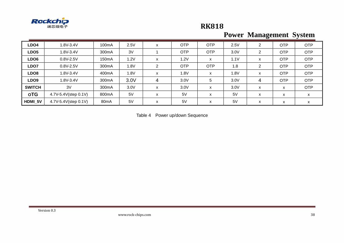
Table 4 Power up/down Sequence
RK818 Power Management System
Version 0.3 www.rock-chips.com 39
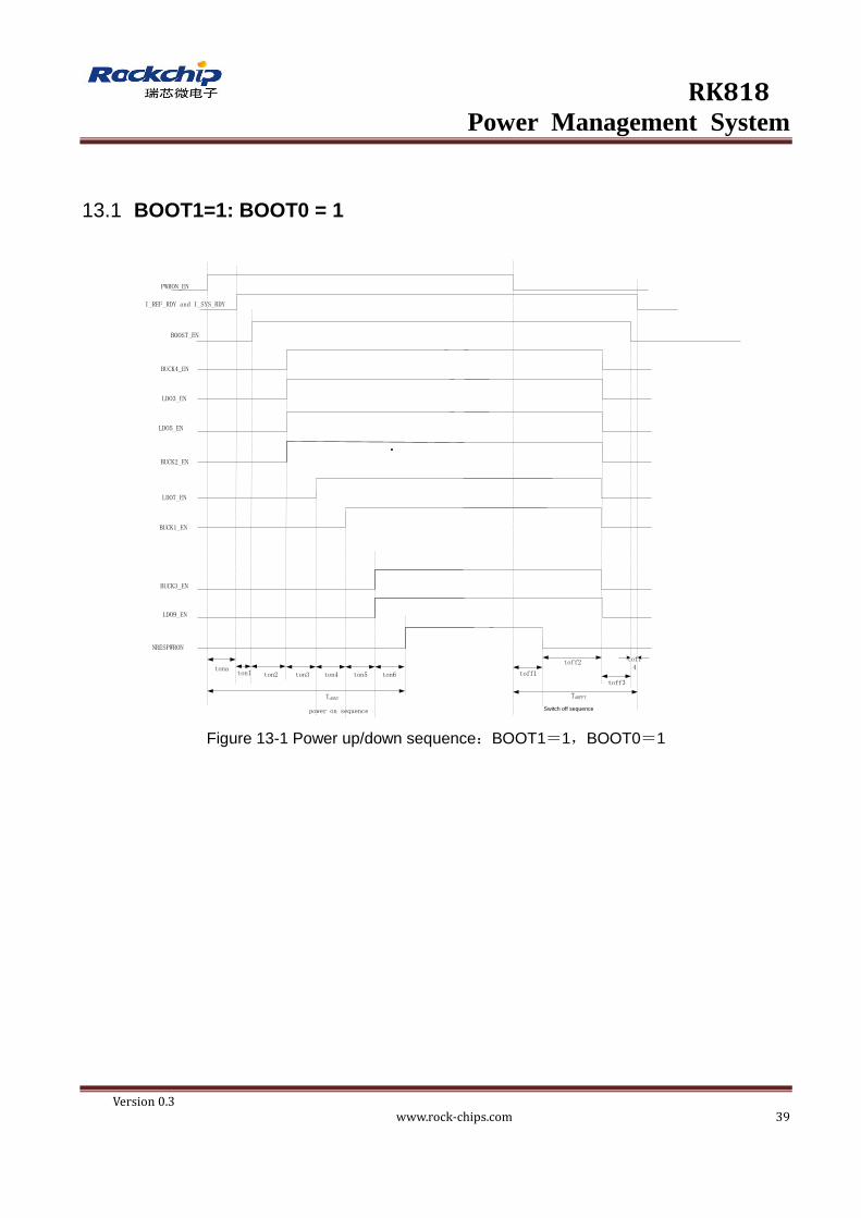
BOOT1=1: BOOT0 = 1 13.1
BOOST_EN
BUCK4_EN
LDO7_EN
LDO3_EN
BUCK1_EN
BUCK2_EN
BUCK3_EN
NRESPWRON
ton1 toff1
toff2
power on sequence
TdONT TdOFFT
Switch off sequence
ton2 ton3 ton4 ton5 ton6
LDO5_EN
LDO9_EN
PWRON_EN
toff3
toff4
I_REF_RDY and I_SYS_RDY
tona
Figure 13-1 Power up/down sequence:BOOT1=1,BOOT0=1
RK818 Power Management System
Version 0.3 www.rock-chips.com 40
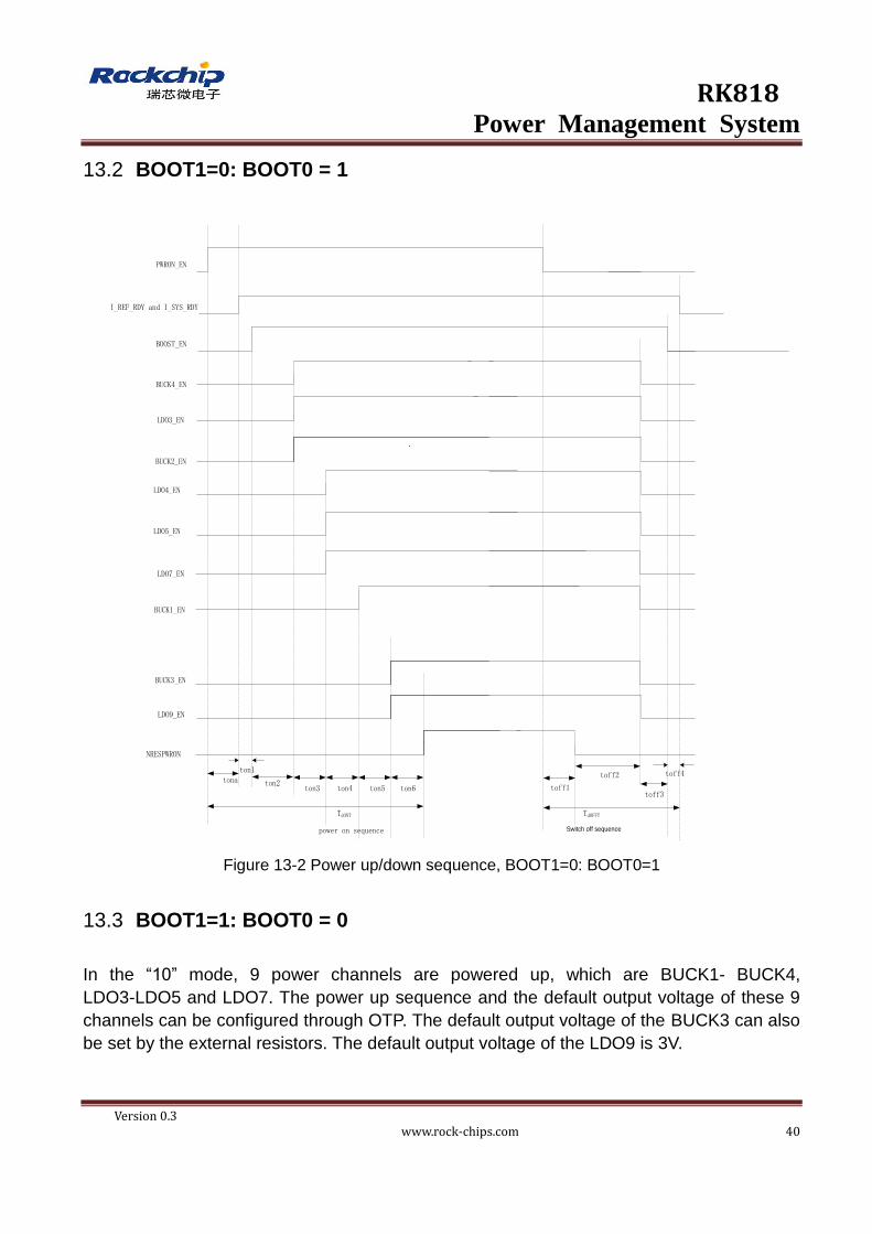
BOOT1=0: BOOT0 = 1 13.2
BOOST_EN
BUCK4_EN
LDO7_EN
LDO3_EN
BUCK1_EN
BUCK2_EN
BUCK3_EN
NRESPWRON
ton1
toff1
toff2
power on sequence
TdONT TdOFFT
Switch off sequence
ton2ton3 ton4 ton5 ton6
LDO5_EN
LDO9_EN
LDO4_EN
toff3
PWRON_EN
I_REF_RDY and I_SYS_RDY
tonatoff4
Figure 13-2 Power up/down sequence, BOOT1=0: BOOT0=1
BOOT1=1: BOOT0 = 0 13.3
In the “10” mode, 9 power channels are powered up, which are BUCK1- BUCK4,
LDO3-LDO5 and LDO7. The power up sequence and the default output voltage of these 9
channels can be configured through OTP. The default output voltage of the BUCK3 can also
be set by the external resistors. The default output voltage of the LDO9 is 3V.
RK818 Power Management System
Version 0.3 www.rock-chips.com 41
BOOT1=0: BOOT0 = 0 13.4
In the mode of “00”, 14 power channels are powered up, among which, the power up
sequence and the default voltage of the BUCK1-4, LDO1-9 and the SWITCH can be
configured through OTP. Again, The default output voltage of the BUCK3 can also be set by
the external resistors. The voltage of the SWITCH is the same as the input supply.
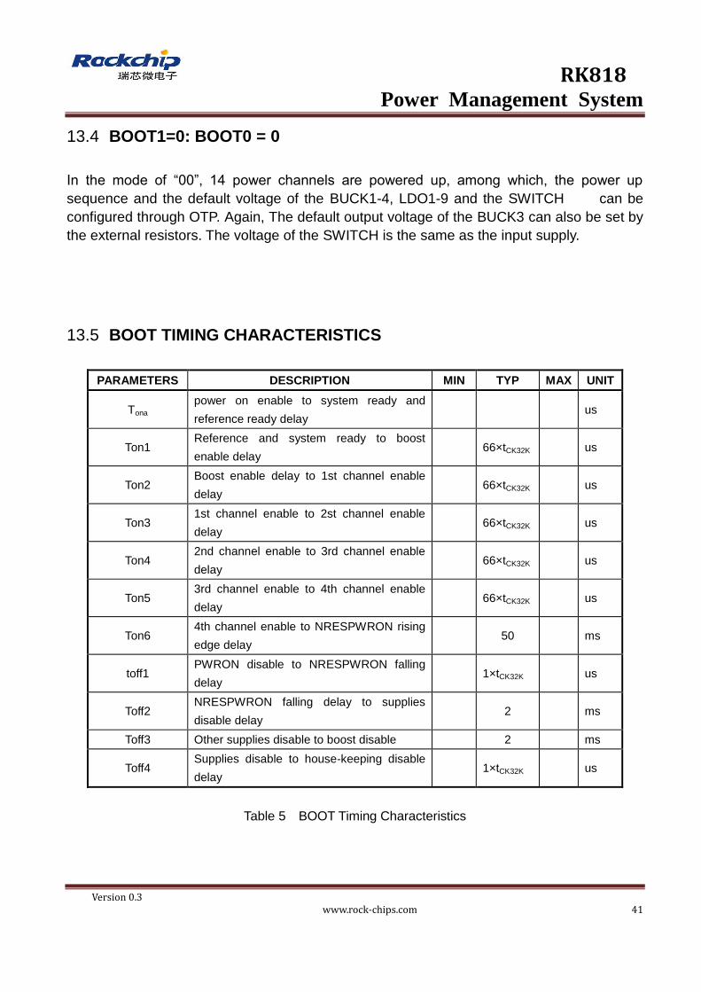
BOOT TIMING CHARACTERISTICS 13.5
PARAMETERS DESCRIPTION MIN TYP MAX UNIT
Tona power on enable to system ready and
reference ready delay us
Ton1 Reference and system ready to boost
enable delay 66×tCK32K us
Ton2 Boost enable delay to 1st channel enable
delay 66×tCK32K us
Ton3 1st channel enable to 2st channel enable
delay 66×tCK32K us
Ton4 2nd channel enable to 3rd channel enable
delay 66×tCK32K us
Ton5 3rd channel enable to 4th channel enable
delay 66×tCK32K us
Ton6 4th channel enable to NRESPWRON rising
edge delay 50 ms
toff1 PWRON disable to NRESPWRON falling
delay 1×tCK32K us
Toff2 NRESPWRON falling delay to supplies
disable delay 2 ms
Toff3 Other supplies disable to boost disable 2 ms
Toff4 Supplies disable to house-keeping disable
delay 1×tCK32K us
Table 5 BOOT Timing Characteristics
RK818 Power Management System
Version 0.3 www.rock-chips.com 42
14 POWER CONTROL TIMING
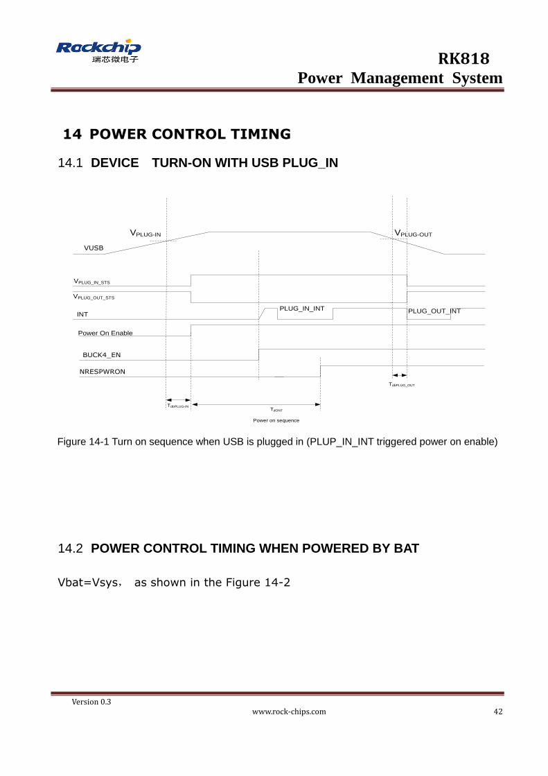
DEVICE TURN-ON WITH USB PLUG_IN 14.1
VUSB
VPLUG-IN
BUCK4_EN
NRESPWRON
TdbPLUG-IN
Power on sequence
VPLUG_IN_STS
TdONT
TdbPLUG_OUT
Power On Enable
VPLUG-OUT
VPLUG_OUT_STS
INTPLUG_IN_INT PLUG_OUT_INT
Figure 14-1 Turn on sequence when USB is plugged in (PLUP_IN_INT triggered power on enable)
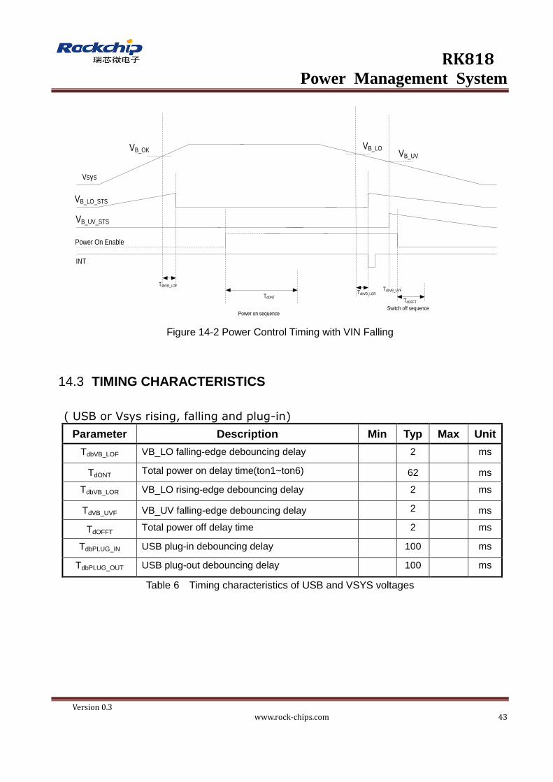
POWER CONTROL TIMING WHEN POWERED BY BAT 14.2
Vbat=Vsys, as shown in the Figure 14-2
RK818 Power Management System
Version 0.3 www.rock-chips.com 43
Vsys
VB_OK VB_UV
TdbVB_LOF
Power on sequence
TdbVB_UVF
Switch off sequence
VB_LO_STS
VB_UV_STS
VB_LO
TdONTTdbVB_LOR
TdOFFT
Power On Enable
INT
Figure 14-2 Power Control Timing with VIN Falling
TIMING CHARACTERISTICS 14.3
( USB or Vsys rising, falling and plug-in)
Parameter Description Min Typ Max Unit
TdbVB_LOF VB_LO falling-edge debouncing delay 2 ms
TdONT Total power on delay time(ton1~ton6) 62 ms
TdbVB_LOR VB_LO rising-edge debouncing delay 2 ms
TdVB_UVF VB_UV falling-edge debouncing delay 2 ms
TdOFFT Total power off delay time 2 ms
TdbPLUG_IN USB plug-in debouncing delay 100 ms
TdbPLUG_OUT USB plug-out debouncing delay 100 ms
Table 6 Timing characteristics of USB and VSYS voltages
RK818 Power Management System
Version 0.3 www.rock-chips.com 44
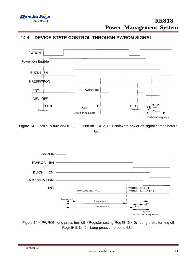
DEVICE STATE CONTROL THROUGH PWRON SIGNAL 14.4
BUCK4_EN
INT
NRESPWRON
Switch on sequence
TdONT
Switch off sequence
TdbPWRONF
PWRON
DEV_OFF
TdbPWRONF toff1
PWRON_INT
Power On Enable
toff2
TdOFFT
Figure 14-3 PWRON turn on/DEV_OFF turn off(DEV_OFF software power off signal comes before
toff1)
BUCK4_EN
INT
NRESPWRON
TdbPWRONF
PWRON
toff1
PWRON_INT=1
TdPWRONLP
TdPWRONLPTO
PWRON_INT=1
PWRON_LP_INT=1
PWRON_EN
toff2
Switch off sequence
TdOFFT
Figure 14-4 PWRON long press turn off(Register setting Reg4B<6>=0:Long press turning off
Reg4B<5:4>=0:Long press time set to 6S)
RK818 Power Management System
Version 0.3 www.rock-chips.com 45
TIMING CHARACTERISTICS (PWRON, DEV_OFF) 14.5
Parameter Description Min Typ Max Unit
TdbPWRONF PWRON falling-edge debouncing delay 500 ms
TdONT Total power on delay time(ton1~ton6) 62 ms
TdPWRONLP PWRON long press delay to interrupt (PWRON
falling edge to PWRON_LP_INT=1)
4 s
TdPWRONLPTO PWRON long press delay to turn off (PWRON
falling edge to NRESPWRON falling edge)
6 s
toff1 POWER ON disable to NRESPWRON falling
delay 1×tCK32K us
Toff2 NRESPWRON falling delay to supplies disable
delay 2 ms
TdOFFT total power off delay time 2 ms
Table 7 PWRON/DEV_OFF timing characteristics
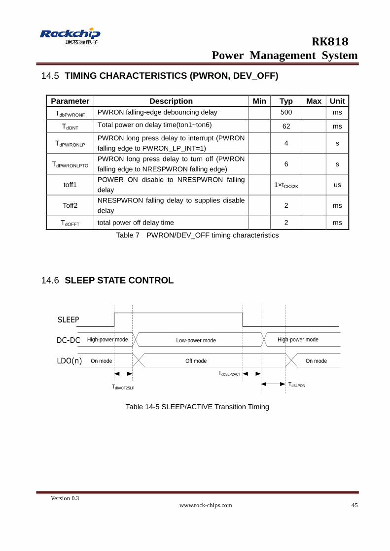
SLEEP STATE CONTROL 14.6
SLEEP
TdbACT2SLP
DC-DC High-power mode Low-power mode High-power mode
LDO(n)
TdbSLP2ACT
TdSLPON
On mode Off mode On mode
Table 14-5 SLEEP/ACTIVE Transition Timing
RK818 Power Management System
Version 0.3 www.rock-chips.com 46
TIMING CHARACTERISTICS (SLEEP) 14.7
Parameter Description Min Typ Max Unit
TdbACT2SLP SLEEP falling-edge debouncing delay 3×tck32k us
TdbSLP2ACT SLEEP rising-edge debouncing delay 3×tck32k us
TdSLPON Delay to turn on enable after SLEEP
rising-edge debouncing
1×tck32k us
Table 8 SLEEP Timing Characteristics
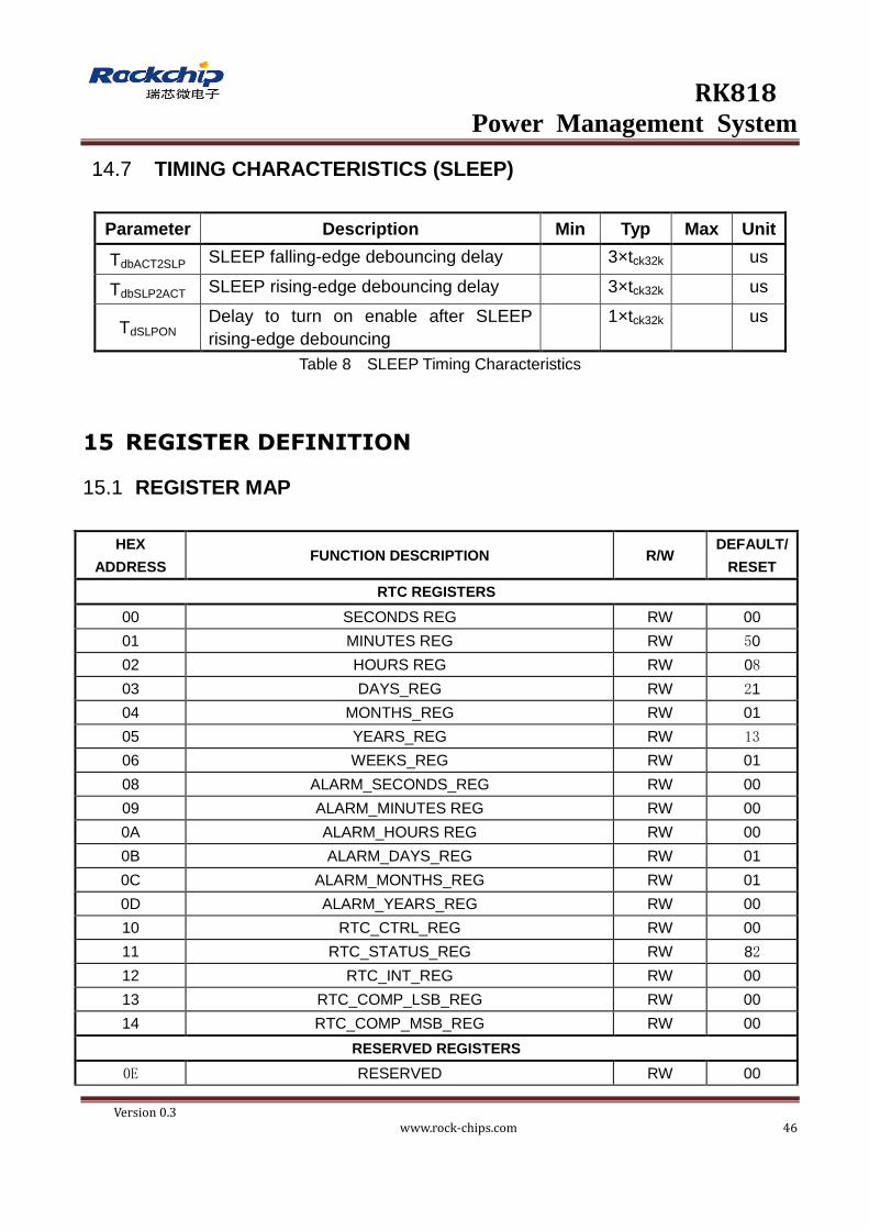
15 REGISTER DEFINITION
REGISTER MAP 15.1
HEX
ADDRESS FUNCTION DESCRIPTION R/W
DEFAULT/
RESET
RTC REGISTERS
00 SECONDS REG RW 00
01 MINUTES REG RW 50
02 HOURS REG RW 08
03 DAYS_REG RW 21
04 MONTHS_REG RW 01
05 YEARS_REG RW 13
06 WEEKS_REG RW 01
08 ALARM_SECONDS_REG RW 00
09 ALARM_MINUTES REG RW 00
0A ALARM_HOURS REG RW 00
0B ALARM_DAYS_REG RW 01
0C ALARM_MONTHS_REG RW 01
0D ALARM_YEARS_REG RW 00
10 RTC_CTRL_REG RW 00
11 RTC_STATUS_REG RW 82
12 RTC_INT_REG RW 00
13 RTC_COMP_LSB_REG RW 00
14 RTC_COMP_MSB_REG RW 00
RESERVED REGISTERS
0E RESERVED RW 00
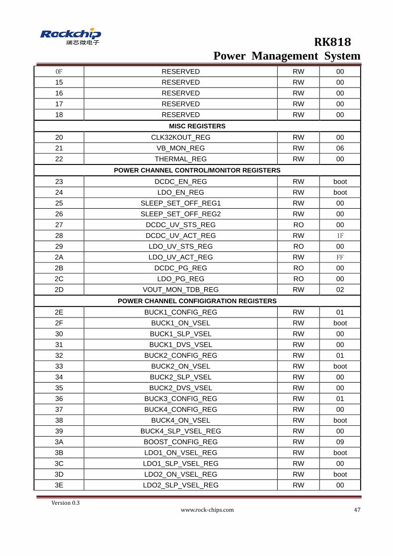
RK818 Power Management System
Version 0.3 www.rock-chips.com 47
0F RESERVED RW 00
15 RESERVED RW 00
16 RESERVED RW 00
17 RESERVED RW 00
18 RESERVED RW 00
MISC REGISTERS
20 CLK32KOUT_REG RW 00
21 VB_MON_REG RW 06
22 THERMAL_REG RW 00
POWER CHANNEL CONTROL/MONITOR REGISTERS
23 DCDC_EN_REG RW boot
24 LDO_EN_REG RW boot
25 SLEEP_SET_OFF_REG1 RW 00
26 SLEEP_SET_OFF_REG2 RW 00
27 DCDC_UV_STS_REG RO 00
28 DCDC_UV_ACT_REG RW 1F
29 LDO_UV_STS_REG RO 00
2A LDO_UV_ACT_REG RW FF
2B DCDC_PG_REG RO 00
2C LDO_PG_REG RO 00
2D VOUT_MON_TDB_REG RW 02
POWER CHANNEL CONFIGIGRATION REGISTERS
2E BUCK1_CONFIG_REG RW 01
2F BUCK1_ON_VSEL RW boot
30 BUCK1_SLP_VSEL RW 00
31 BUCK1_DVS_VSEL RW 00
32 BUCK2_CONFIG_REG RW 01
33 BUCK2_ON_VSEL RW boot
34 BUCK2_SLP_VSEL RW 00
35 BUCK2_DVS_VSEL RW 00
36 BUCK3_CONFIG_REG RW 01
37 BUCK4_CONFIG_REG RW 00
38 BUCK4_ON_VSEL RW boot
39 BUCK4_SLP_VSEL_REG RW 00
3A BOOST_CONFIG_REG RW 09
3B LDO1_ON_VSEL_REG RW boot
3C LDO1_SLP_VSEL_REG RW 00
3D LDO2_ON_VSEL_REG RW boot
3E LDO2_SLP_VSEL_REG RW 00
RK818 Power Management System
Version 0.3 www.rock-chips.com 48
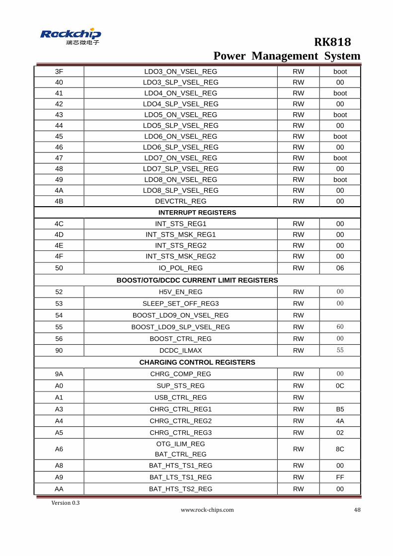
3F LDO3_ON_VSEL_REG RW boot
40 LDO3_SLP_VSEL_REG RW 00
41 LDO4_ON_VSEL_REG RW boot
42 LDO4_SLP_VSEL_REG RW 00
43 LDO5_ON_VSEL_REG RW boot
44 LDO5_SLP_VSEL_REG RW 00
45 LDO6_ON_VSEL_REG RW boot
46 LDO6_SLP_VSEL_REG RW 00
47 LDO7_ON_VSEL_REG RW boot
48 LDO7_SLP_VSEL_REG RW 00
49 LDO8_ON_VSEL_REG RW boot
4A LDO8_SLP_VSEL_REG RW 00
4B DEVCTRL_REG RW 00
INTERRUPT REGISTERS
4C INT_STS_REG1 RW 00
4D INT_STS_MSK_REG1 RW 00
4E INT_STS_REG2 RW 00
4F INT_STS_MSK_REG2 RW 00
50 IO_POL_REG RW 06
BOOST/OTG/DCDC CURRENT LIMIT REGISTERS
52 H5V_EN_REG RW 00
53 SLEEP_SET_OFF_REG3 RW 00
54 BOOST_LDO9_ON_VSEL_REG RW
55 BOOST_LDO9_SLP_VSEL_REG RW 60
56 BOOST_CTRL_REG RW 00
90 DCDC_ILMAX RW 55
CHARGING CONTROL REGISTERS
9A CHRG_COMP_REG RW 00
A0 SUP_STS_REG RW 0C
A1 USB_CTRL_REG RW
A3 CHRG_CTRL_REG1 RW B5
A4 CHRG_CTRL_REG2 RW 4A
A5 CHRG_CTRL_REG3 RW 02
A6 OTG_ILIM_REG
BAT_CTRL_REG RW 8C
A8 BAT_HTS_TS1_REG RW 00
A9 BAT_LTS_TS1_REG RW FF
AA BAT_HTS_TS2_REG RW 00
RK818 Power Management System
Version 0.3 www.rock-chips.com 49
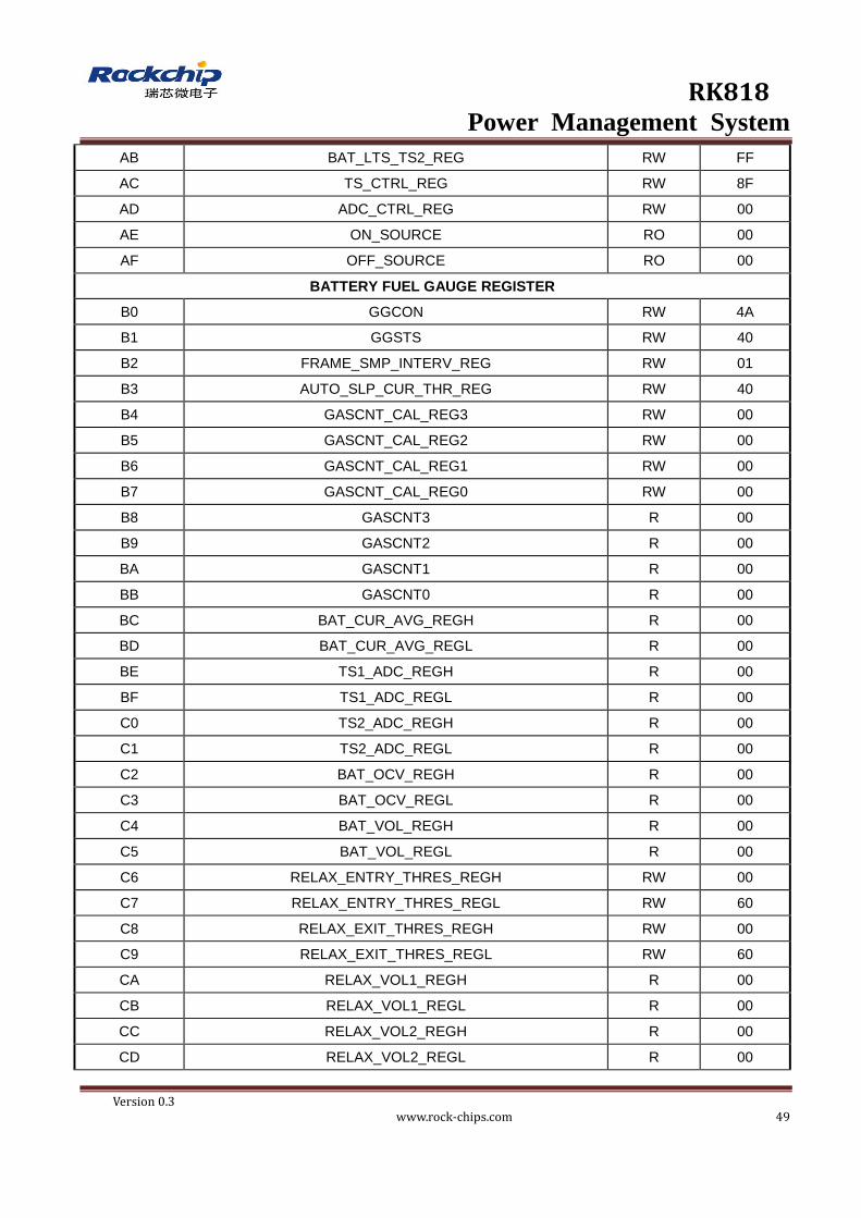
AB BAT_LTS_TS2_REG RW FF
AC TS_CTRL_REG RW 8F
AD ADC_CTRL_REG RW 00
AE ON_SOURCE RO 00
AF OFF_SOURCE RO 00
BATTERY FUEL GAUGE REGISTER
B0 GGCON RW 4A
B1 GGSTS RW 40
B2 FRAME_SMP_INTERV_REG RW 01
B3 AUTO_SLP_CUR_THR_REG RW 40
B4 GASCNT_CAL_REG3 RW 00
B5 GASCNT_CAL_REG2 RW 00
B6 GASCNT_CAL_REG1 RW 00
B7 GASCNT_CAL_REG0 RW 00
B8 GASCNT3 R 00
B9 GASCNT2 R 00
BA GASCNT1 R 00
BB GASCNT0 R 00
BC BAT_CUR_AVG_REGH R 00
BD BAT_CUR_AVG_REGL R 00
BE TS1_ADC_REGH R 00
BF TS1_ADC_REGL R 00
C0 TS2_ADC_REGH R 00
C1 TS2_ADC_REGL R 00
C2 BAT_OCV_REGH R 00
C3 BAT_OCV_REGL R 00
C4 BAT_VOL_REGH R 00
C5 BAT_VOL_REGL R 00
C6 RELAX_ENTRY_THRES_REGH RW 00
C7 RELAX_ENTRY_THRES_REGL RW 60
C8 RELAX_EXIT_THRES_REGH RW 00
C9 RELAX_EXIT_THRES_REGL RW 60
CA RELAX_VOL1_REGH R 00
CB RELAX_VOL1_REGL R 00
CC RELAX_VOL2_REGH R 00
CD RELAX_VOL2_REGL R 00
RK818 Power Management System
Version 0.3 www.rock-chips.com 50
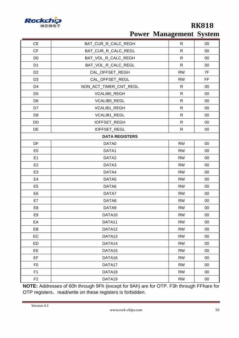
CE BAT_CUR_R_CALC_REGH R 00
CF BAT_CUR_R_CALC_REGL R 00
D0 BAT_VOL_R_CALC_REGH R 00
D1 BAT_VOL_R_CALC_REGL R 00
D2 CAL_OFFSET_REGH RW 7F
D3 CAL_OFFSET_REGL RW FF
D4 NON_ACT_TIMER_CNT_REGL R 00
D5 VCALIB0_REGH R 00
D6 VCALIB0_REGL R 00
D7 VCALIB1_REGH R 00
D8 VCALIB1_REGL R 00
DD IOFFSET_REGH R 00
DE IOFFSET_REGL R 00
DATA REGISTERS
DF DATA0 RW 00
E0 DATA1 RW 00
E1 DATA2 RW 00
E2 DATA3 RW 00
E3 DATA4 RW 00
E4 DATA5 RW 00
E5 DATA6 RW 00
E6 DATA7 RW 00
E7 DATA8 RW 00
E8 DATA9 RW 00
E9 DATA10 RW 00
EA DATA11 RW 00
EB DATA12 RW 00
EC DATA13 RW 00
ED DATA14 RW 00
EE DATA15 RW 00
EF DATA16 RW 00
F0 DATA17 RW 00
F1 DATA18 RW 00
F2 DATA19 RW 00
NOTE: Addresses of 60h through 9Fh (except for 9Ah) are for OTP. F3h through FFhare for
OTP registers,read/write on these registers is forbidden.
RK818 Power Management System
Version 0.3 www.rock-chips.com 51
REGISTER DESCRIPTION 15.2
RTC REGISTER 15.2.1
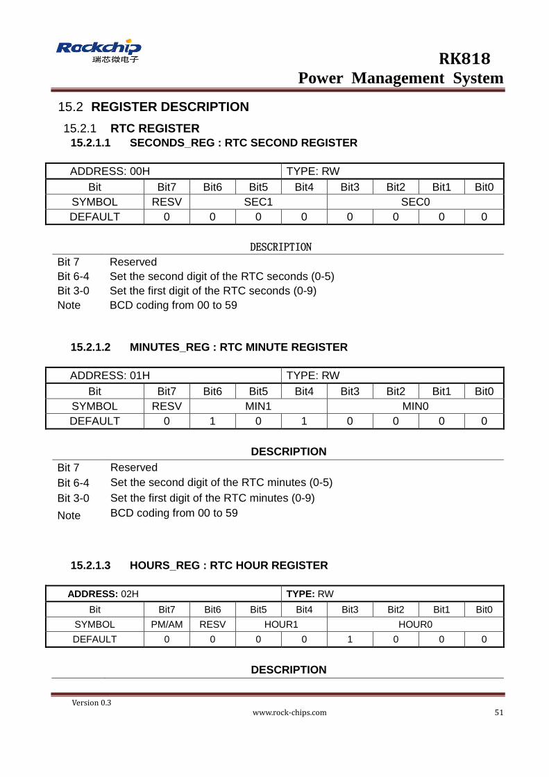
SECONDS_REG : RTC SECOND REGISTER 15.2.1.1
ADDRESS: 00H TYPE: RW
Bit Bit7 Bit6 Bit5 Bit4 Bit3 Bit2 Bit1 Bit0
SYMBOL RESV SEC1 SEC0
DEFAULT 0 0 0 0 0 0 0 0
DESCRIPTION
Bit 7 Reserved
Bit 6-4 Set the second digit of the RTC seconds (0-5)
Bit 3-0 Set the first digit of the RTC seconds (0-9)
Note BCD coding from 00 to 59
MINUTES_REG : RTC MINUTE REGISTER 15.2.1.2
ADDRESS: 01H TYPE: RW
Bit Bit7 Bit6 Bit5 Bit4 Bit3 Bit2 Bit1 Bit0
SYMBOL RESV MIN1 MIN0
DEFAULT 0 1 0 1 0 0 0 0
DESCRIPTION
Bit 7 Reserved
Bit 6-4 Set the second digit of the RTC minutes (0-5)
Bit 3-0 Set the first digit of the RTC minutes (0-9)
Note BCD coding from 00 to 59
HOURS_REG : RTC HOUR REGISTER 15.2.1.3
ADDRESS: 02H TYPE: RW
Bit Bit7 Bit6 Bit5 Bit4 Bit3 Bit2 Bit1 Bit0
SYMBOL PM/AM RESV HOUR1 HOUR0
DEFAULT 0 0 0 0 1 0 0 0
DESCRIPTION
RK818 Power Management System
Version 0.3 www.rock-chips.com 52
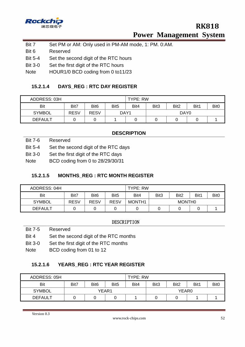
Bit 7 Set PM or AM: Only used in PM-AM mode, 1: PM. 0:AM.
Bit 6 Reserved
Bit 5-4 Set the second digit of the RTC hours
Bit 3-0 Set the first digit of the RTC hours
Note HOUR1/0 BCD coding from 0 to11/23
DAYS_REG : RTC DAY REGISTER 15.2.1.4
ADDRESS: 03H TYPE: RW
Bit Bit7 Bit6 Bit5 Bit4 Bit3 Bit2 Bit1 Bit0
SYMBOL RESV RESV DAY1 DAY0
DEFAULT 0 0 1 0 0 0 0 1
DESCRIPTION
Bit 7-6 Reserved
Bit 5-4 Set the second digit of the RTC days
Bit 3-0 Set the first digit of the RTC days
Note BCD coding from 0 to 28/29/30/31
MONTHS_REG : RTC MONTH REGISTER 15.2.1.5
ADDRESS: 04H TYPE: RW
Bit Bit7 Bit6 Bit5 Bit4 Bit3 Bit2 Bit1 Bit0
SYMBOL RESV RESV RESV MONTH1 MONTH0
DEFAULT 0 0 0 0 0 0 0 1
DESCRIPTION
Bit 7-5 Reserved
Bit 4 Set the second digit of the RTC months
Bit 3-0 Set the first digit of the RTC months
Note BCD coding from 01 to 12
YEARS_REG : RTC YEAR REGISTER 15.2.1.6
ADDRESS: 05H TYPE: RW
Bit Bit7 Bit6 Bit5 Bit4 Bit3 Bit2 Bit1 Bit0
SYMBOL YEAR1 YEAR0
DEFAULT 0 0 0 1 0 0 1 1
RK818 Power Management System
Version 0.3 www.rock-chips.com 53
DESCRIPTION
Bit 7-5 Set the second digit of the RTC years
Bit 3-0 Set the first digit of the RTC years
Note BCD coding from 00 to 99
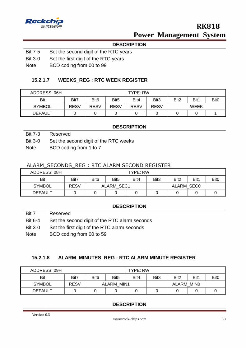
WEEKS_REG : RTC WEEK REGISTER 15.2.1.7
ADDRESS: 06H TYPE: RW
Bit Bit7 Bit6 Bit5 Bit4 Bit3 Bit2 Bit1 Bit0
SYMBOL RESV RESV RESV RESV RESV WEEK
DEFAULT 0 0 0 0 0 0 0 1
DESCRIPTION
Bit 7-3 Reserved
Bit 3-0 Set the second digit of the RTC weeks
Note BCD coding from 1 to 7
ALARM_SECONDS_REG : RTC ALARM SECOND REGISTER
ADDRESS: 08H TYPE: RW
Bit Bit7 Bit6 Bit5 Bit4 Bit3 Bit2 Bit1 Bit0
SYMBOL RESV ALARM_SEC1 ALARM_SEC0
DEFAULT 0 0 0 0 0 0 0 0
DESCRIPTION
Bit 7 Reserved
Bit 6-4 Set the second digit of the RTC alarm seconds
Bit 3-0 Set the first digit of the RTC alarm seconds
Note BCD coding from 00 to 59
ALARM_MINUTES_REG : RTC ALARM MINUTE REGISTER 15.2.1.8
ADDRESS: 09H TYPE: RW
Bit Bit7 Bit6 Bit5 Bit4 Bit3 Bit2 Bit1 Bit0
SYMBOL RESV ALARM_MIN1 ALARM_MIN0
DEFAULT 0 0 0 0 0 0 0 0
DESCRIPTION
RK818 Power Management System
Version 0.3 www.rock-chips.com 54
Bit 7 Reserved
Bit 6-4 Set the second digit of the RTC alarm minutes
Bit 3-0 Set the first digit of the RTC alarm minutes
Note BCD coding from 00 to 59
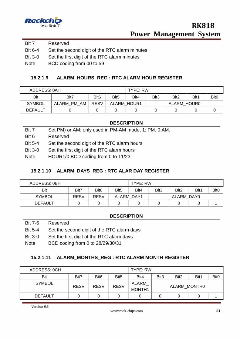
ALARM_HOURS_REG : RTC ALARM HOUR REGISTER 15.2.1.9
ADDRESS: 0AH TYPE: RW
Bit Bit7 Bit6 Bit5 Bit4 Bit3 Bit2 Bit1 Bit0
SYMBOL ALARM_PM_AM RESV ALARM_HOUR1 ALARM_HOUR0
DEFAULT 0 0 0 0 0 0 0 0
DESCRIPTION
Bit 7 Set PM) or AM: only used in PM-AM mode, 1: PM. 0:AM.
Bit 6 Reserved
Bit 5-4 Set the second digit of the RTC alarm hours
Bit 3-0 Set the first digit of the RTC alarm hours
Note HOUR1/0 BCD coding from 0 to 11/23
ALARM_DAYS_REG : RTC ALAR DAY REGISTER 15.2.1.10
ADDRESS: 0BH TYPE: RW
Bit Bit7 Bit6 Bit5 Bit4 Bit3 Bit2 Bit1 Bit0
SYMBOL RESV RESV ALARM_DAY1 ALARM_DAY0
DEFAULT 0 0 0 0 0 0 0 1
DESCRIPTION
Bit 7-6 Reserved
Bit 5-4 Set the second digit of the RTC alarm days
Bit 3-0 Set the first digit of the RTC alarm days
Note BCD coding from 0 to 28/29/30/31
ALARM_MONTHS_REG : RTC ALARM MONTH REGISTER 15.2.1.11
ADDRESS: 0CH TYPE: RW
Bit Bit7 Bit6 Bit5 Bit4 Bit3 Bit2 Bit1 Bit0
SYMBOL RESV RESV RESV
ALARM_
MONTH1 ALARM_MONTH0
DEFAULT 0 0 0 0 0 0 0 1
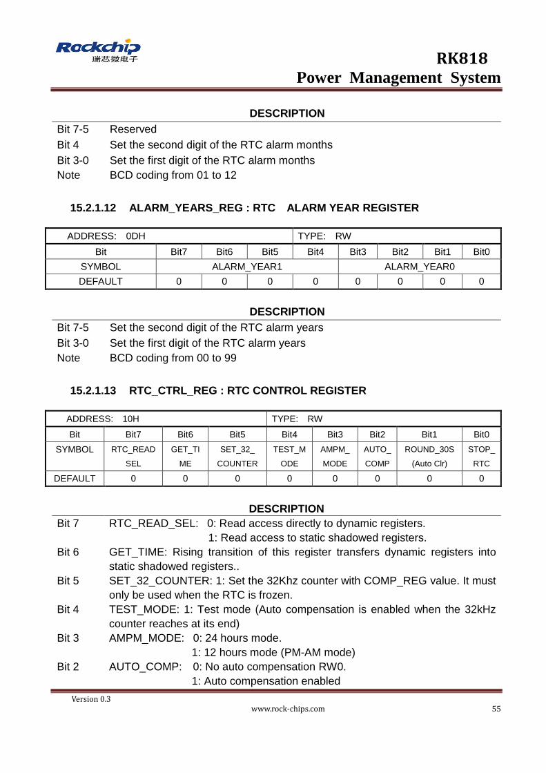
RK818 Power Management System
Version 0.3 www.rock-chips.com 55
DESCRIPTION
Bit 7-5 Reserved
Bit 4 Set the second digit of the RTC alarm months
Bit 3-0 Set the first digit of the RTC alarm months
Note BCD coding from 01 to 12
ALARM_YEARS_REG : RTC ALARM YEAR REGISTER 15.2.1.12
ADDRESS: 0DH TYPE: RW
Bit Bit7 Bit6 Bit5 Bit4 Bit3 Bit2 Bit1 Bit0
SYMBOL ALARM_YEAR1 ALARM_YEAR0
DEFAULT 0 0 0 0 0 0 0 0
DESCRIPTION
Bit 7-5 Set the second digit of the RTC alarm years
Bit 3-0 Set the first digit of the RTC alarm years
Note BCD coding from 00 to 99
RTC_CTRL_REG : RTC CONTROL REGISTER 15.2.1.13
ADDRESS: 10H TYPE: RW
Bit Bit7 Bit6 Bit5 Bit4 Bit3 Bit2 Bit1 Bit0
SYMBOL RTC_READ
SEL
GET_TI
ME
SET_32_
COUNTER
TEST_M
ODE
AMPM_
MODE
AUTO_
COMP
ROUND_30S
(Auto Clr)
STOP_
RTC
DEFAULT 0 0 0 0 0 0 0 0
DESCRIPTION
Bit 7 RTC_READ_SEL: 0: Read access directly to dynamic registers.
1: Read access to static shadowed registers.
Bit 6 GET_TIME: Rising transition of this register transfers dynamic registers into
static shadowed registers..
Bit 5 SET_32_COUNTER: 1: Set the 32Khz counter with COMP_REG value. It must
only be used when the RTC is frozen.
Bit 4 TEST_MODE: 1: Test mode (Auto compensation is enabled when the 32kHz
counter reaches at its end)
Bit 3 AMPM_MODE: 0: 24 hours mode.
1: 12 hours mode (PM-AM mode)
Bit 2 AUTO_COMP: 0: No auto compensation RW0.
1: Auto compensation enabled
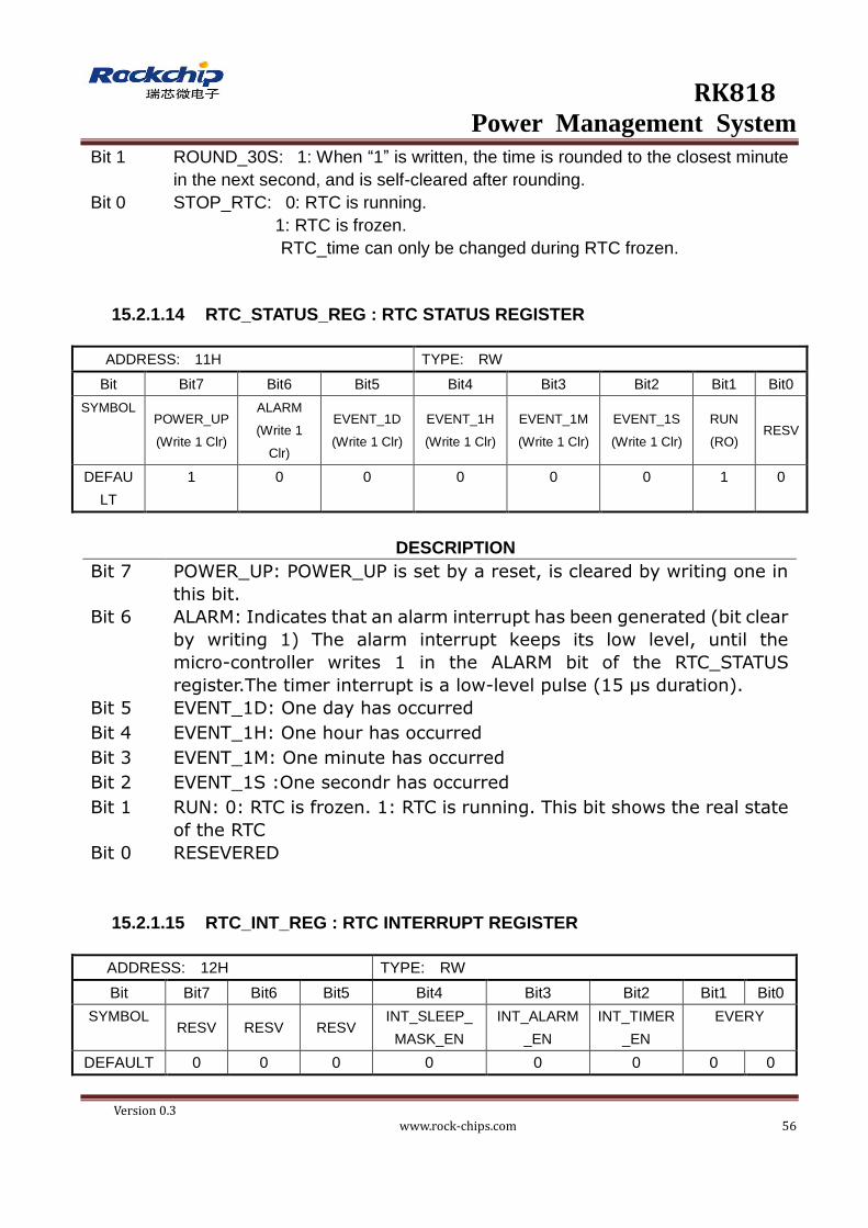
RK818 Power Management System
Version 0.3 www.rock-chips.com 56
Bit 1 ROUND_30S: 1: When “1” is written, the time is rounded to the closest minute
in the next second, and is self-cleared after rounding.
Bit 0 STOP_RTC: 0: RTC is running.
1: RTC is frozen.
RTC_time can only be changed during RTC frozen.
RTC_STATUS_REG : RTC STATUS REGISTER 15.2.1.14
ADDRESS: 11H TYPE: RW
Bit Bit7 Bit6 Bit5 Bit4 Bit3 Bit2 Bit1 Bit0
SYMBOL POWER_UP
(Write 1 Clr)
ALARM
(Write 1
Clr)
EVENT_1D
(Write 1 Clr)
EVENT_1H
(Write 1 Clr)
EVENT_1M
(Write 1 Clr)
EVENT_1S
(Write 1 Clr)
RUN
(RO) RESV
DEFAU
LT
1 0 0 0 0 0 1 0
DESCRIPTION
Bit 7 POWER_UP: POWER_UP is set by a reset, is cleared by writing one in
this bit.
Bit 6 ALARM: Indicates that an alarm interrupt has been generated (bit clear
by writing 1) The alarm interrupt keeps its low level, until the
micro-controller writes 1 in the ALARM bit of the RTC_STATUS
register.The timer interrupt is a low-level pulse (15 μs duration).
Bit 5 EVENT_1D: One day has occurred
Bit 4 EVENT_1H: One hour has occurred
Bit 3 EVENT_1M: One minute has occurred
Bit 2 EVENT_1S :One secondr has occurred
Bit 1 RUN: 0: RTC is frozen. 1: RTC is running. This bit shows the real state
of the RTC
Bit 0 RESEVERED
RTC_INT_REG : RTC INTERRUPT REGISTER 15.2.1.15
ADDRESS: 12H TYPE: RW
Bit Bit7 Bit6 Bit5 Bit4 Bit3 Bit2 Bit1 Bit0
SYMBOL RESV RESV RESV
INT_SLEEP_
MASK_EN
INT_ALARM
_EN
INT_TIMER
_EN
EVERY
DEFAULT 0 0 0 0 0 0 0 0
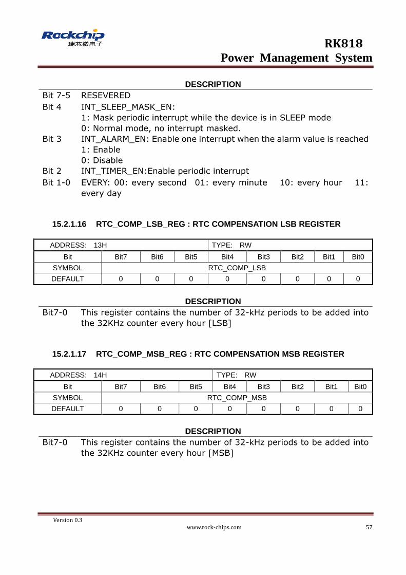
RK818 Power Management System
Version 0.3 www.rock-chips.com 57
DESCRIPTION
Bit 7-5 RESEVERED
Bit 4 INT_SLEEP_MASK_EN:
1: Mask periodic interrupt while the device is in SLEEP mode
0: Normal mode, no interrupt masked.
Bit 3 INT_ALARM_EN: Enable one interrupt when the alarm value is reached
1: Enable
0: Disable
Bit 2 INT_TIMER_EN:Enable periodic interrupt
Bit 1-0 EVERY: 00: every second 01: every minute 10: every hour 11:
every day
RTC_COMP_LSB_REG : RTC COMPENSATION LSB REGISTER 15.2.1.16
ADDRESS: 13H TYPE: RW
Bit Bit7 Bit6 Bit5 Bit4 Bit3 Bit2 Bit1 Bit0
SYMBOL RTC_COMP_LSB
DEFAULT 0 0 0 0 0 0 0 0
DESCRIPTION
Bit7-0 This register contains the number of 32-kHz periods to be added into
the 32KHz counter every hour [LSB]
RTC_COMP_MSB_REG : RTC COMPENSATION MSB REGISTER 15.2.1.17
ADDRESS: 14H TYPE: RW
Bit Bit7 Bit6 Bit5 Bit4 Bit3 Bit2 Bit1 Bit0
SYMBOL RTC_COMP_MSB
DEFAULT 0 0 0 0 0 0 0 0
DESCRIPTION
Bit7-0 This register contains the number of 32-kHz periods to be added into
the 32KHz counter every hour [MSB]
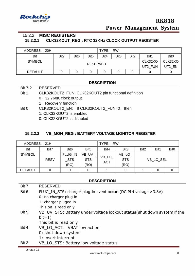
RK818 Power Management System
Version 0.3 www.rock-chips.com 58
MISC REGISTERS 15.2.2
CLK32KOUT_REG : RTC 32KHz CLOCK OUTPUT REGISTER 15.2.2.1
ADDRESS: 20H TYPE: RW
Bit Bit7 Bit6 Bit5 Bit4 Bit3 Bit2 Bit1 Bit0
SYMBOL RESERVED
CLK32KO
UT2_FUN
CLK32KO
UT2_EN
DEFAULT 0 0 0 0 0 0 0 0
DESCRIPTION
Bit 7-2
Bit 1
RESERVED
CLK32KOUT2_FUN: CLK32KOUT2 pin functional definition
0:32.768K clock output
1:Recovery function
Bit 0 CLK32KOUT2_EN: If CLK32KOUT2_FUN=0,then
1: CLK32KOUT2 is enabled
0: CLK32KOUT2 is disabled
VB_MON_REG : BATTERY VOLTAGE MONITOR REGISTER 15.2.2.2
ADDRESS: 21H TYPE: RW
Bit Bit7 Bit6 Bit5 Bit4 Bit3 Bit2 Bit1 Bit0
SYMBOL
RESV
PLUG_IN
_STS
(RO)
VB_UV_
STS
(RO)
VB_LO_
ACT
VB_LO_
STS
(RO)
VB_LO_SEL
DEFAULT 0 0 0 1 0 1 0 0
DESCRIPTION
Bit 7 RESERVED
Bit 6 PLUG_IN_STS: charger plug-in event occurs(DC PIN voltage >3.8V)
0: no charger plug in
1: charger pluged in
This bit is read only
Bit 5 VB_UV_STS: Battery under voltage lockout status(shut down system if the
bit=1)
This bit is read only
Bit 4 VB_LO_ACT: VBAT low action
0: shut down system
1: insert interrupt
Bit 3 VB_LO_STS: Battery low voltage status
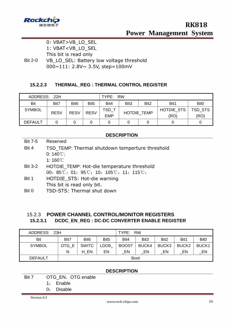
RK818 Power Management System
Version 0.3 www.rock-chips.com 59
0: VBAT>VB_LO_SEL
1: VBAT<VB_LO_SEL
This bit is read only
Bit 2-0 VB_LO_SEL: Battery low voltage threshold
000~111: 2.8V~ 3.5V, step=100mV
THERMAL_REG : THERMAL CONTROL REGISTER 15.2.2.3
ADDRESS: 22H TYPE: RW
Bit Bit7 Bit6 Bit5 Bit4 Bit3 Bit2 Bit1 Bit0
SYMBOL RESV RESV RESV
TSD_T
EMP HOTDIE_TEMP
HOTDIE_STS
(RO)
TSD_STS
(RO)
DEFAULT 0 0 0 0 0 0 0 0
DESCRIPTION
Bit 7-5 Reserved
Bit 4 TSD_TEMP: Thermal shutdown temperture threshold
0: 140;
1: 160
Bit 3-2 HOTDIE_TEMP: Hot-die temperature threshold
00:85;01:95;10:105;11:115;
Bit 1 HOTDIE_STS: Hot-die warning
This bit is read only bit.
Bit 0 TSD-STS: Thermal shut down
POWER CHANNEL CONTROL/MONITOR REGISTERS 15.2.3 DCDC_EN_REG : DC-DC CONVERTER ENABLE REGISTER 15.2.3.1
ADDRESS: 23H TYPE: RW
Bit Bit7 Bit6 Bit5 Bit4 Bit3 Bit2 Bit1 Bit0
SYMBOL OTG_E
N
SWITC
H_EN
LDO9_
EN
BOOST
_EN
BUCK4
_EN
BUCK3
_EN
BUCK2
_EN
BUCK1
_EN
DEFAULT Boot
DESCRIPTION
Bit 7
OTG_EN,OTG enable
1: Enable
0: Disable
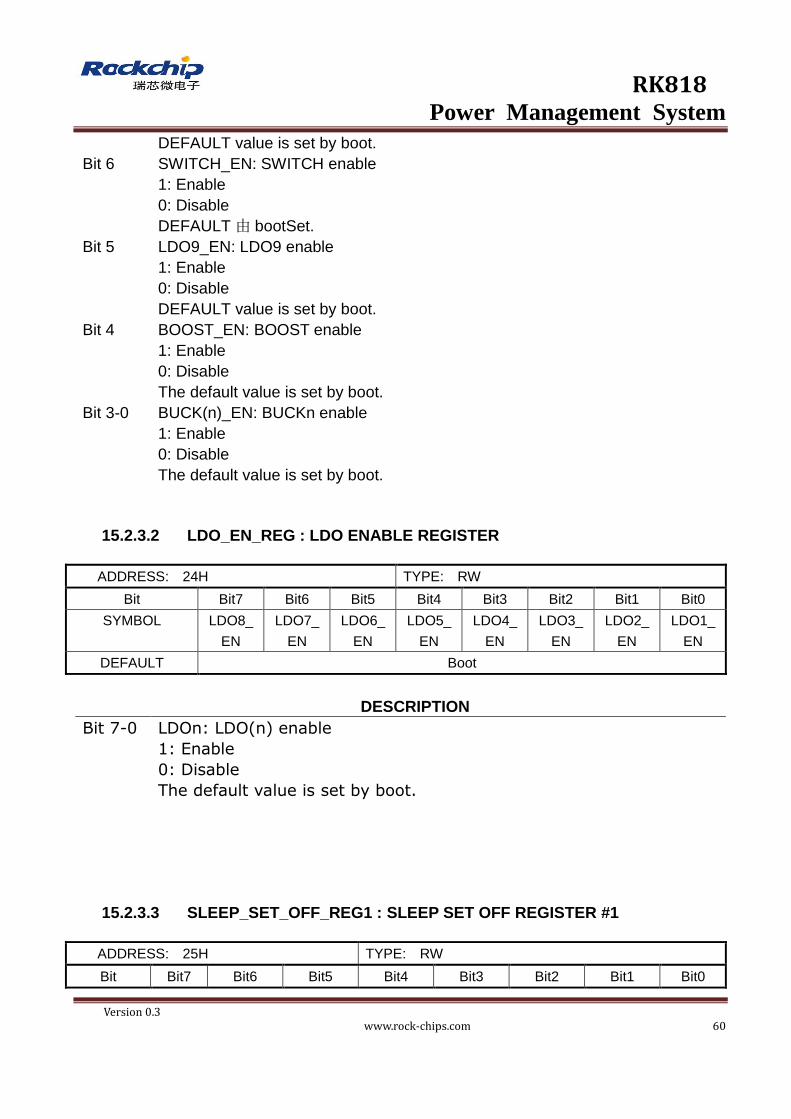
RK818 Power Management System
Version 0.3 www.rock-chips.com 60
Bit 6
DEFAULT value is set by boot.
SWITCH_EN: SWITCH enable
1: Enable
0: Disable
DEFAULT 由 bootSet.
Bit 5 LDO9_EN: LDO9 enable
1: Enable
0: Disable
DEFAULT value is set by boot.
Bit 4 BOOST_EN: BOOST enable
1: Enable
0: Disable
The default value is set by boot.
Bit 3-0 BUCK(n)_EN: BUCKn enable
1: Enable
0: Disable
The default value is set by boot.
LDO_EN_REG : LDO ENABLE REGISTER 15.2.3.2
ADDRESS: 24H TYPE: RW
Bit Bit7 Bit6 Bit5 Bit4 Bit3 Bit2 Bit1 Bit0
SYMBOL LDO8_
EN
LDO7_
EN
LDO6_
EN
LDO5_
EN
LDO4_
EN
LDO3_
EN
LDO2_
EN
LDO1_
EN
DEFAULT Boot
DESCRIPTION
Bit 7-0 LDOn: LDO(n) enable
1: Enable
0: Disable
The default value is set by boot.
SLEEP_SET_OFF_REG1 : SLEEP SET OFF REGISTER #1 15.2.3.3
ADDRESS: 25H TYPE: RW
Bit Bit7 Bit6 Bit5 Bit4 Bit3 Bit2 Bit1 Bit0
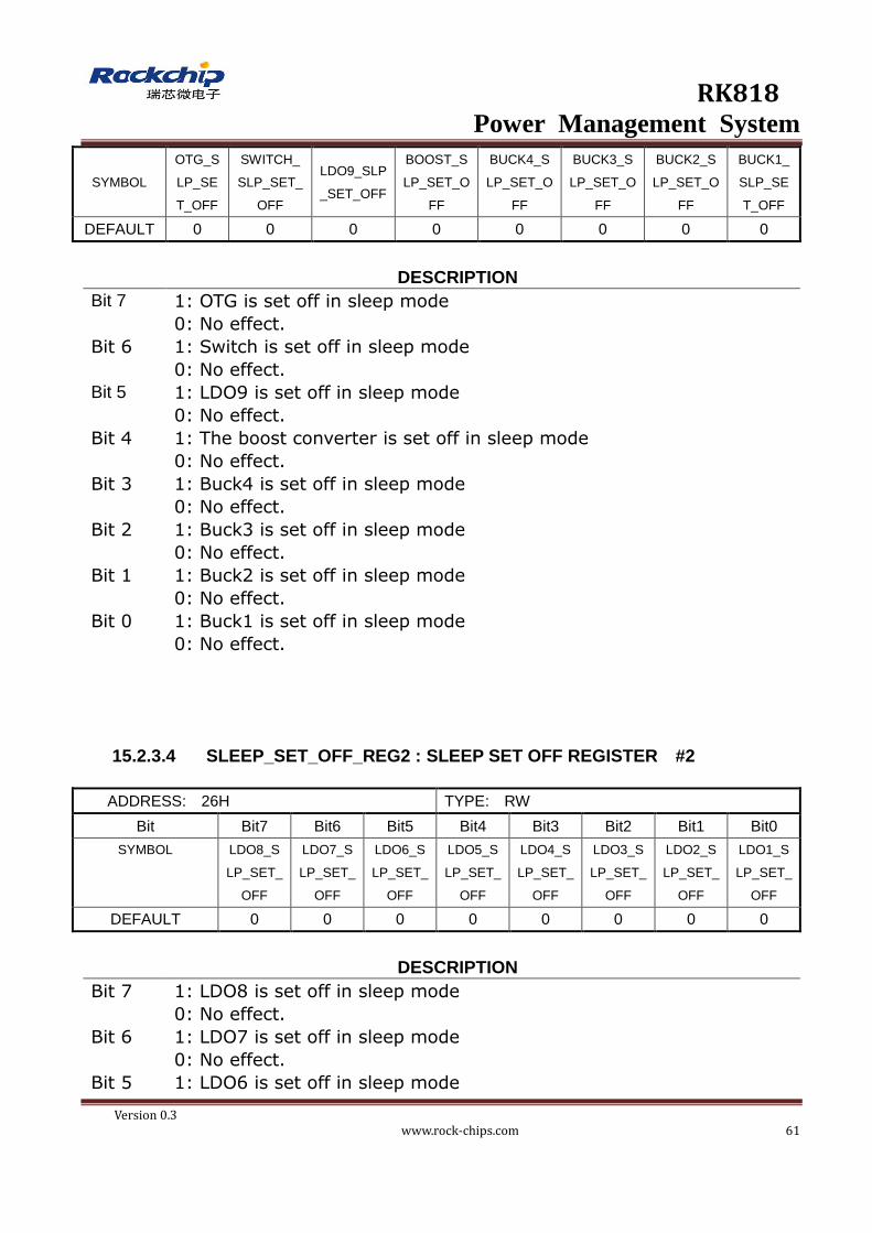
RK818 Power Management System
Version 0.3 www.rock-chips.com 61
SYMBOL
OTG_S
LP_SE
T_OFF
SWITCH_
SLP_SET_
OFF
LDO9_SLP
_SET_OFF
BOOST_S
LP_SET_O
FF
BUCK4_S
LP_SET_O
FF
BUCK3_S
LP_SET_O
FF
BUCK2_S
LP_SET_O
FF
BUCK1_
SLP_SE
T_OFF
DEFAULT 0 0 0 0 0 0 0 0
DESCRIPTION
Bit 7 1: OTG is set off in sleep mode
0: No effect.
Bit 6 1: Switch is set off in sleep mode
0: No effect.
Bit 5 1: LDO9 is set off in sleep mode
0: No effect.
Bit 4 1: The boost converter is set off in sleep mode
0: No effect.
Bit 3 1: Buck4 is set off in sleep mode
0: No effect.
Bit 2 1: Buck3 is set off in sleep mode
0: No effect.
Bit 1 1: Buck2 is set off in sleep mode
0: No effect.
Bit 0 1: Buck1 is set off in sleep mode
0: No effect.
SLEEP_SET_OFF_REG2 : SLEEP SET OFF REGISTER #2 15.2.3.4
ADDRESS: 26H TYPE: RW
Bit Bit7 Bit6 Bit5 Bit4 Bit3 Bit2 Bit1 Bit0
SYMBOL LDO8_S
LP_SET_
OFF
LDO7_S
LP_SET_
OFF
LDO6_S
LP_SET_
OFF
LDO5_S
LP_SET_
OFF
LDO4_S
LP_SET_
OFF
LDO3_S
LP_SET_
OFF
LDO2_S
LP_SET_
OFF
LDO1_S
LP_SET_
OFF
DEFAULT 0 0 0 0 0 0 0 0
DESCRIPTION
Bit 7 1: LDO8 is set off in sleep mode
0: No effect.
Bit 6 1: LDO7 is set off in sleep mode
0: No effect.
Bit 5 1: LDO6 is set off in sleep mode
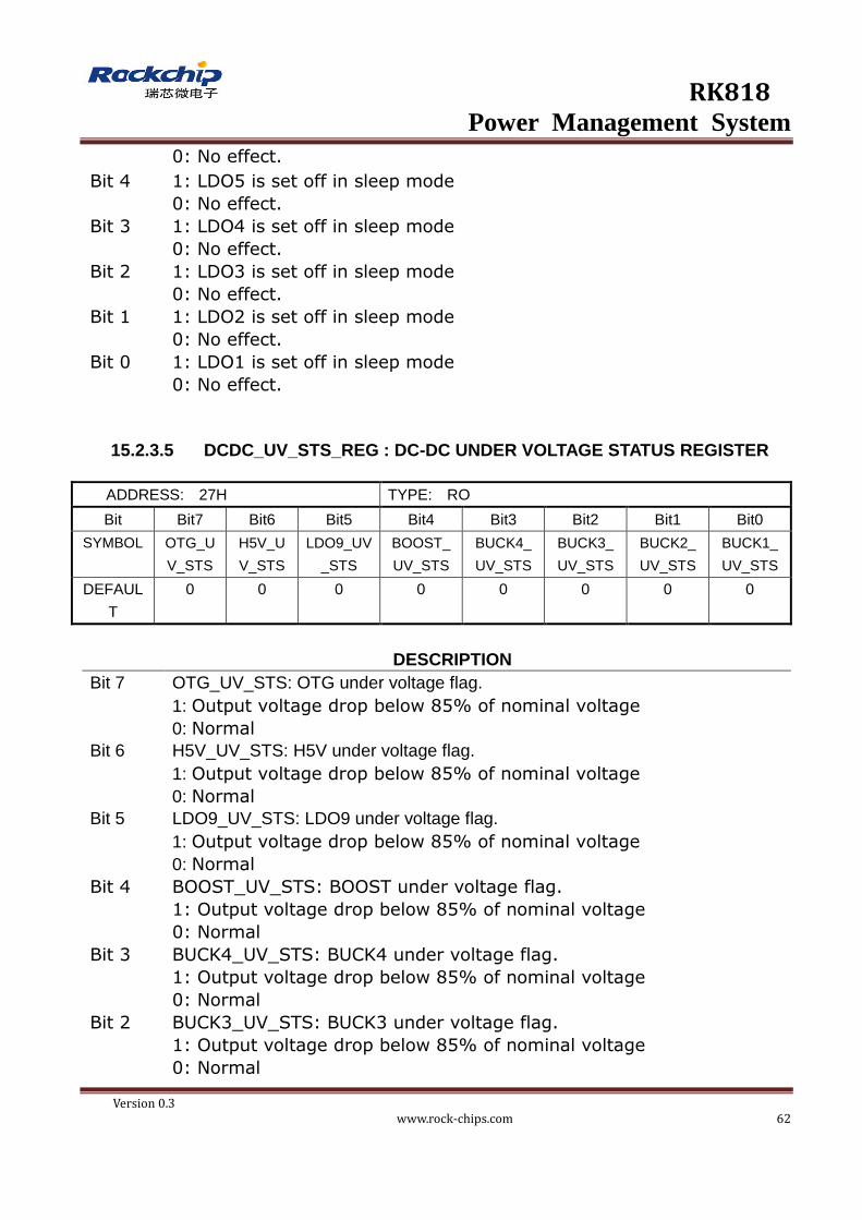
RK818 Power Management System
Version 0.3 www.rock-chips.com 62
0: No effect.
Bit 4 1: LDO5 is set off in sleep mode
0: No effect.
Bit 3 1: LDO4 is set off in sleep mode
0: No effect.
Bit 2 1: LDO3 is set off in sleep mode
0: No effect.
Bit 1 1: LDO2 is set off in sleep mode
0: No effect.
Bit 0 1: LDO1 is set off in sleep mode
0: No effect.
DCDC_UV_STS_REG : DC-DC UNDER VOLTAGE STATUS REGISTER 15.2.3.5
ADDRESS: 27H TYPE: RO
Bit Bit7 Bit6 Bit5 Bit4 Bit3 Bit2 Bit1 Bit0
SYMBOL OTG_U
V_STS
H5V_U
V_STS
LDO9_UV
_STS
BOOST_
UV_STS
BUCK4_
UV_STS
BUCK3_
UV_STS
BUCK2_
UV_STS
BUCK1_
UV_STS
DEFAUL
T
0 0 0 0 0 0 0 0
DESCRIPTION
Bit 7 OTG_UV_STS: OTG under voltage flag.
1: Output voltage drop below 85% of nominal voltage
0: Normal
Bit 6 H5V_UV_STS: H5V under voltage flag.
1: Output voltage drop below 85% of nominal voltage
0: Normal
Bit 5 LDO9_UV_STS: LDO9 under voltage flag.
1: Output voltage drop below 85% of nominal voltage
0: Normal
Bit 4 BOOST_UV_STS: BOOST under voltage flag.
1: Output voltage drop below 85% of nominal voltage
0: Normal
Bit 3 BUCK4_UV_STS: BUCK4 under voltage flag.
1: Output voltage drop below 85% of nominal voltage
0: Normal
Bit 2 BUCK3_UV_STS: BUCK3 under voltage flag.
1: Output voltage drop below 85% of nominal voltage
0: Normal
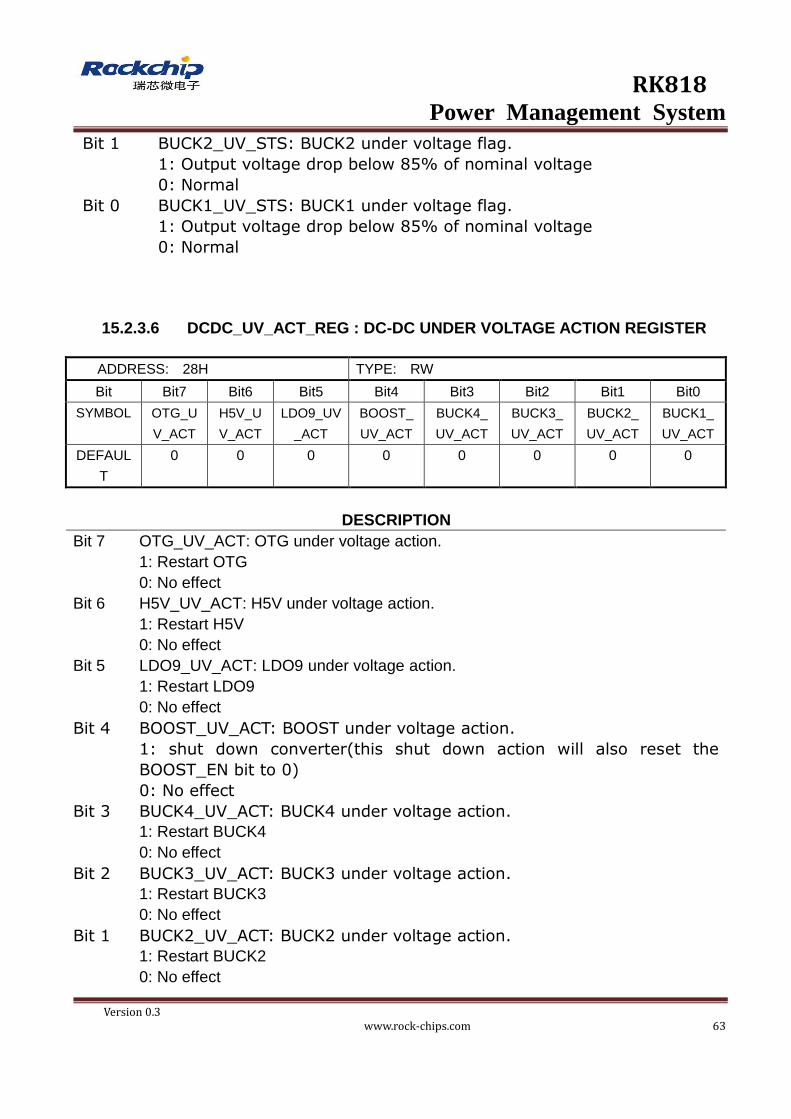
RK818 Power Management System
Version 0.3 www.rock-chips.com 63
Bit 1 BUCK2_UV_STS: BUCK2 under voltage flag.
1: Output voltage drop below 85% of nominal voltage
0: Normal
Bit 0 BUCK1_UV_STS: BUCK1 under voltage flag.
1: Output voltage drop below 85% of nominal voltage
0: Normal
DCDC_UV_ACT_REG : DC-DC UNDER VOLTAGE ACTION REGISTER 15.2.3.6
ADDRESS: 28H TYPE: RW
Bit Bit7 Bit6 Bit5 Bit4 Bit3 Bit2 Bit1 Bit0
SYMBOL OTG_U
V_ACT
H5V_U
V_ACT
LDO9_UV
_ACT
BOOST_
UV_ACT
BUCK4_
UV_ACT
BUCK3_
UV_ACT
BUCK2_
UV_ACT
BUCK1_
UV_ACT
DEFAUL
T
0 0 0 0 0 0 0 0
DESCRIPTION
Bit 7 OTG_UV_ACT: OTG under voltage action.
1: Restart OTG
0: No effect
Bit 6 H5V_UV_ACT: H5V under voltage action.
1: Restart H5V
0: No effect
Bit 5 LDO9_UV_ACT: LDO9 under voltage action.
1: Restart LDO9
0: No effect
Bit 4 BOOST_UV_ACT: BOOST under voltage action.
1: shut down converter(this shut down action will also reset the
BOOST_EN bit to 0)
0: No effect
Bit 3 BUCK4_UV_ACT: BUCK4 under voltage action.
1: Restart BUCK4
0: No effect
Bit 2 BUCK3_UV_ACT: BUCK3 under voltage action.
1: Restart BUCK3
0: No effect
Bit 1 BUCK2_UV_ACT: BUCK2 under voltage action.
1: Restart BUCK2
0: No effect
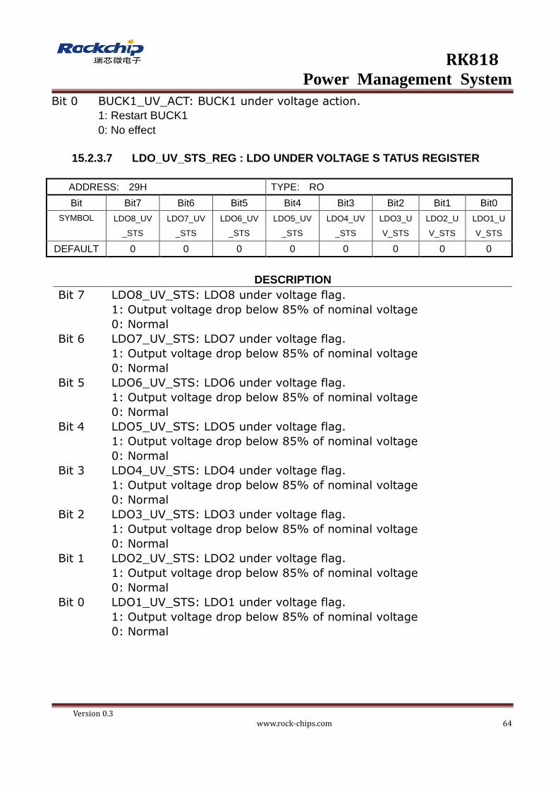
RK818 Power Management System
Version 0.3 www.rock-chips.com 64
Bit 0 BUCK1_UV_ACT: BUCK1 under voltage action.
1: Restart BUCK1
0: No effect
LDO_UV_STS_REG : LDO UNDER VOLTAGE S TATUS REGISTER 15.2.3.7
ADDRESS: 29H TYPE: RO
Bit Bit7 Bit6 Bit5 Bit4 Bit3 Bit2 Bit1 Bit0
SYMBOL LDO8_UV
_STS
LDO7_UV
_STS
LDO6_UV
_STS
LDO5_UV
_STS
LDO4_UV
_STS
LDO3_U
V_STS
LDO2_U
V_STS
LDO1_U
V_STS
DEFAULT 0 0 0 0 0 0 0 0
DESCRIPTION
Bit 7 LDO8_UV_STS: LDO8 under voltage flag.
1: Output voltage drop below 85% of nominal voltage
0: Normal
Bit 6 LDO7_UV_STS: LDO7 under voltage flag.
1: Output voltage drop below 85% of nominal voltage
0: Normal
Bit 5 LDO6_UV_STS: LDO6 under voltage flag.
1: Output voltage drop below 85% of nominal voltage
0: Normal
Bit 4 LDO5_UV_STS: LDO5 under voltage flag.
1: Output voltage drop below 85% of nominal voltage
0: Normal
Bit 3 LDO4_UV_STS: LDO4 under voltage flag.
1: Output voltage drop below 85% of nominal voltage
0: Normal
Bit 2 LDO3_UV_STS: LDO3 under voltage flag.
1: Output voltage drop below 85% of nominal voltage
0: Normal
Bit 1 LDO2_UV_STS: LDO2 under voltage flag.
1: Output voltage drop below 85% of nominal voltage
0: Normal
Bit 0 LDO1_UV_STS: LDO1 under voltage flag.
1: Output voltage drop below 85% of nominal voltage
0: Normal
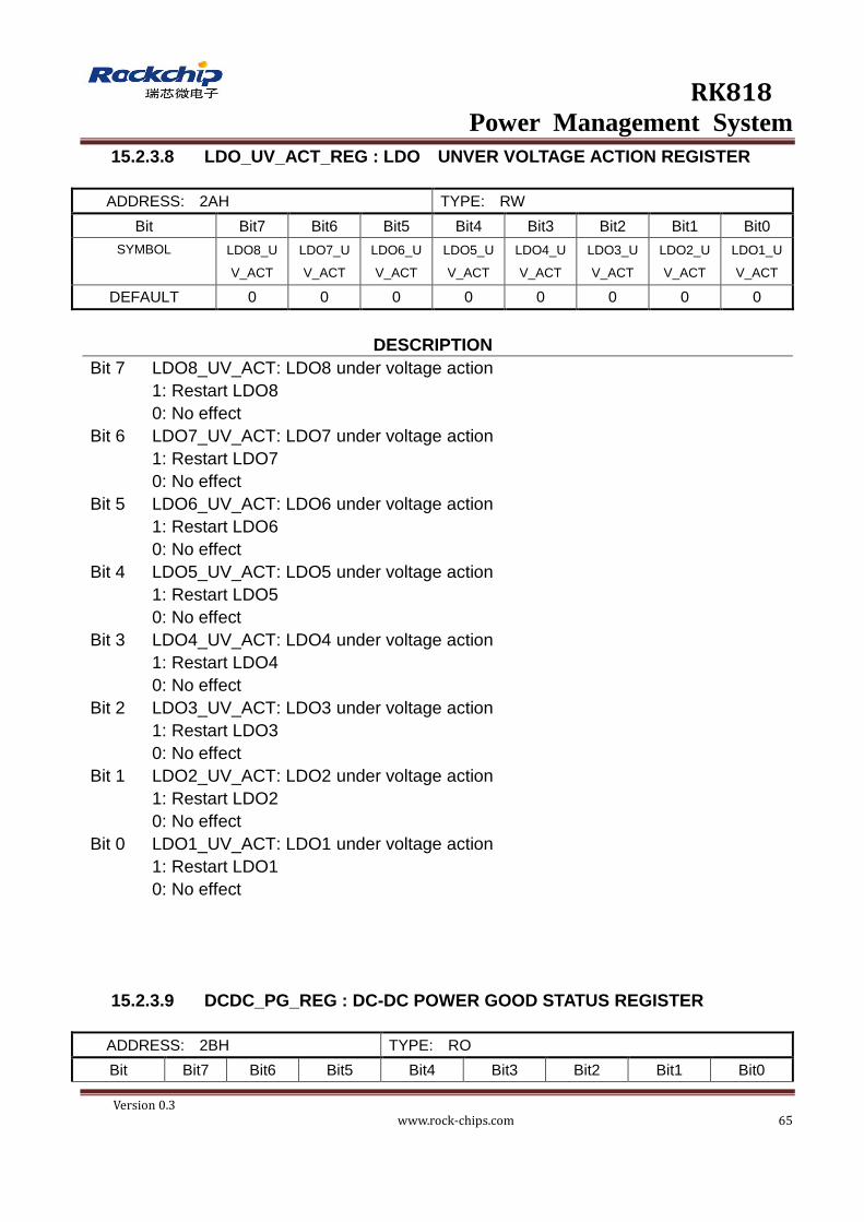
RK818 Power Management System
Version 0.3 www.rock-chips.com 65
LDO_UV_ACT_REG : LDO UNVER VOLTAGE ACTION REGISTER 15.2.3.8
ADDRESS: 2AH TYPE: RW
Bit Bit7 Bit6 Bit5 Bit4 Bit3 Bit2 Bit1 Bit0
SYMBOL LDO8_U
V_ACT
LDO7_U
V_ACT
LDO6_U
V_ACT
LDO5_U
V_ACT
LDO4_U
V_ACT
LDO3_U
V_ACT
LDO2_U
V_ACT
LDO1_U
V_ACT
DEFAULT 0 0 0 0 0 0 0 0
DESCRIPTION
Bit 7 LDO8_UV_ACT: LDO8 under voltage action
1: Restart LDO8
0: No effect
Bit 6 LDO7_UV_ACT: LDO7 under voltage action
1: Restart LDO7
0: No effect
Bit 5 LDO6_UV_ACT: LDO6 under voltage action
1: Restart LDO6
0: No effect
Bit 4 LDO5_UV_ACT: LDO5 under voltage action
1: Restart LDO5
0: No effect
Bit 3 LDO4_UV_ACT: LDO4 under voltage action
1: Restart LDO4
0: No effect
Bit 2 LDO3_UV_ACT: LDO3 under voltage action
1: Restart LDO3
0: No effect
Bit 1 LDO2_UV_ACT: LDO2 under voltage action
1: Restart LDO2
0: No effect
Bit 0 LDO1_UV_ACT: LDO1 under voltage action
1: Restart LDO1
0: No effect
DCDC_PG_REG : DC-DC POWER GOOD STATUS REGISTER 15.2.3.9
ADDRESS: 2BH TYPE: RO
Bit Bit7 Bit6 Bit5 Bit4 Bit3 Bit2 Bit1 Bit0
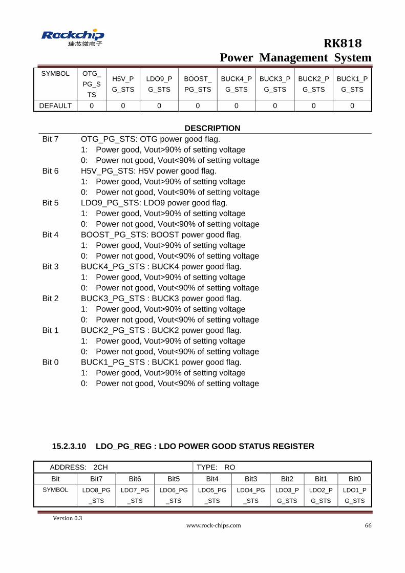
RK818 Power Management System
Version 0.3 www.rock-chips.com 66
SYMBOL OTG_
PG_S
TS
H5V_P
G_STS
LDO9_P
G_STS
BOOST_
PG_STS
BUCK4_P
G_STS
BUCK3_P
G_STS
BUCK2_P
G_STS
BUCK1_P
G_STS
DEFAULT 0 0 0 0 0 0 0 0
DESCRIPTION
Bit 7 OTG_PG_STS: OTG power good flag.
1: Power good, Vout>90% of setting voltage
0: Power not good, Vout<90% of setting voltage
Bit 6 H5V_PG_STS: H5V power good flag.
1: Power good, Vout>90% of setting voltage
0: Power not good, Vout<90% of setting voltage
Bit 5 LDO9_PG_STS: LDO9 power good flag.
1: Power good, Vout>90% of setting voltage
0: Power not good, Vout<90% of setting voltage
Bit 4 BOOST_PG_STS: BOOST power good flag.
1: Power good, Vout>90% of setting voltage
0: Power not good, Vout<90% of setting voltage
Bit 3 BUCK4_PG_STS : BUCK4 power good flag.
1: Power good, Vout>90% of setting voltage
0: Power not good, Vout<90% of setting voltage
Bit 2 BUCK3_PG_STS : BUCK3 power good flag.
1: Power good, Vout>90% of setting voltage
0: Power not good, Vout<90% of setting voltage
Bit 1 BUCK2_PG_STS : BUCK2 power good flag.
1: Power good, Vout>90% of setting voltage
0: Power not good, Vout<90% of setting voltage
Bit 0 BUCK1_PG_STS : BUCK1 power good flag.
1: Power good, Vout>90% of setting voltage
0: Power not good, Vout<90% of setting voltage
LDO_PG_REG : LDO POWER GOOD STATUS REGISTER 15.2.3.10
ADDRESS: 2CH TYPE: RO
Bit Bit7 Bit6 Bit5 Bit4 Bit3 Bit2 Bit1 Bit0
SYMBOL LDO8_PG
_STS
LDO7_PG
_STS
LDO6_PG
_STS
LDO5_PG
_STS
LDO4_PG
_STS
LDO3_P
G_STS
LDO2_P
G_STS
LDO1_P
G_STS
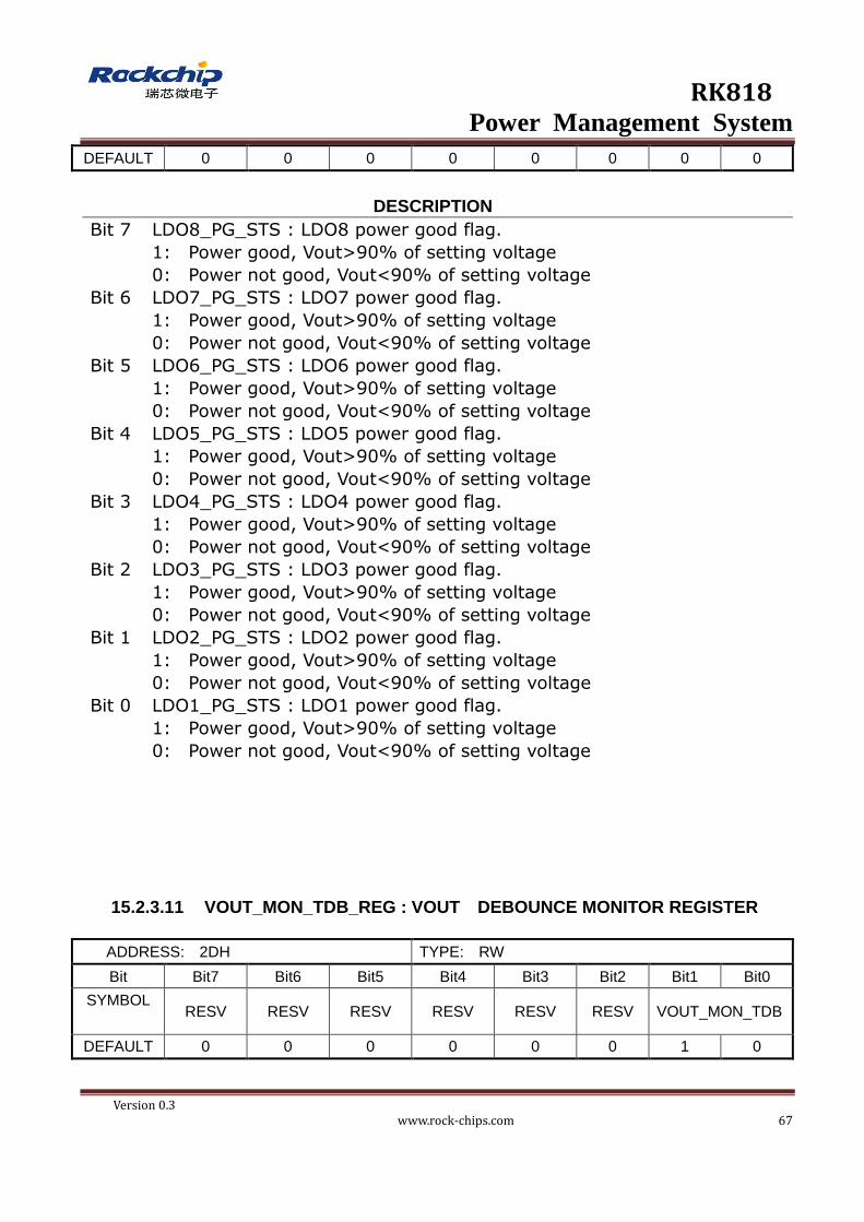
RK818 Power Management System
Version 0.3 www.rock-chips.com 67
DEFAULT 0 0 0 0 0 0 0 0
DESCRIPTION
Bit 7 LDO8_PG_STS : LDO8 power good flag.
1: Power good, Vout>90% of setting voltage
0: Power not good, Vout<90% of setting voltage
Bit 6 LDO7_PG_STS : LDO7 power good flag.
1: Power good, Vout>90% of setting voltage
0: Power not good, Vout<90% of setting voltage
Bit 5 LDO6_PG_STS : LDO6 power good flag.
1: Power good, Vout>90% of setting voltage
0: Power not good, Vout<90% of setting voltage
Bit 4 LDO5_PG_STS : LDO5 power good flag.
1: Power good, Vout>90% of setting voltage
0: Power not good, Vout<90% of setting voltage
Bit 3 LDO4_PG_STS : LDO4 power good flag.
1: Power good, Vout>90% of setting voltage
0: Power not good, Vout<90% of setting voltage
Bit 2 LDO3_PG_STS : LDO3 power good flag.
1: Power good, Vout>90% of setting voltage
0: Power not good, Vout<90% of setting voltage
Bit 1 LDO2_PG_STS : LDO2 power good flag.
1: Power good, Vout>90% of setting voltage
0: Power not good, Vout<90% of setting voltage
Bit 0 LDO1_PG_STS : LDO1 power good flag.
1: Power good, Vout>90% of setting voltage
0: Power not good, Vout<90% of setting voltage
VOUT_MON_TDB_REG : VOUT DEBOUNCE MONITOR REGISTER 15.2.3.11
ADDRESS: 2DH TYPE: RW
Bit Bit7 Bit6 Bit5 Bit4 Bit3 Bit2 Bit1 Bit0
SYMBOL RESV RESV RESV RESV RESV RESV VOUT_MON_TDB
DEFAULT 0 0 0 0 0 0 1 0
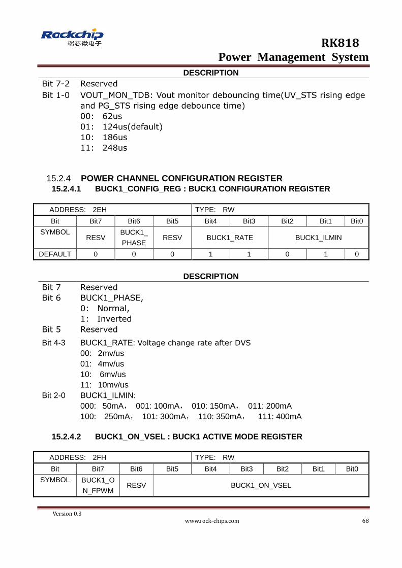
RK818 Power Management System
Version 0.3 www.rock-chips.com 68
DESCRIPTION
Bit 7-2 Reserved
Bit 1-0 VOUT_MON_TDB: Vout monitor debouncing time(UV_STS rising edge
and PG_STS rising edge debounce time)
00: 62us
01: 124us(default)
10: 186us
11: 248us
POWER CHANNEL CONFIGURATION REGISTER 15.2.4 BUCK1_CONFIG_REG : BUCK1 CONFIGURATION REGISTER 15.2.4.1
ADDRESS: 2EH TYPE: RW
Bit Bit7 Bit6 Bit5 Bit4 Bit3 Bit2 Bit1 Bit0
SYMBOL RESV
BUCK1_
PHASE RESV BUCK1_RATE BUCK1_ILMIN
DEFAULT 0 0 0 1 1 0 1 0
DESCRIPTION
Bit 7 Reserved
Bit 6 BUCK1_PHASE,
0: Normal,
1: Inverted
Bit 5 Reserved
Bit 4-3 BUCK1_RATE: Voltage change rate after DVS
00: 2mv/us
01: 4mv/us
10: 6mv/us
11: 10mv/us
Bit 2-0 BUCK1_ILMIN:
000: 50mA, 001: 100mA, 010: 150mA, 011: 200mA
100: 250mA, 101: 300mA, 110: 350mA, 111: 400mA
BUCK1_ON_VSEL : BUCK1 ACTIVE MODE REGISTER 15.2.4.2
ADDRESS: 2FH TYPE: RW
Bit Bit7 Bit6 Bit5 Bit4 Bit3 Bit2 Bit1 Bit0
SYMBOL BUCK1_O
N_FPWM RESV BUCK1_ON_VSEL
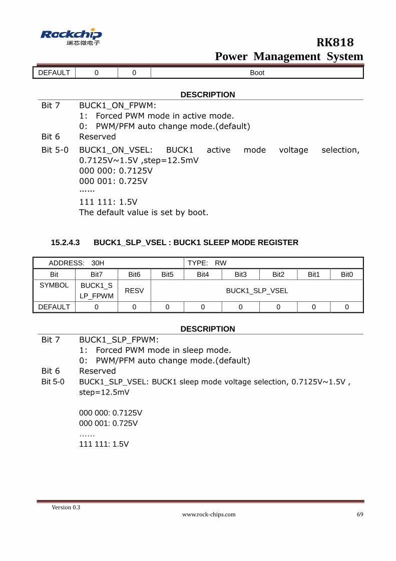
RK818 Power Management System
Version 0.3 www.rock-chips.com 69
DEFAULT 0 0 Boot
DESCRIPTION
Bit 7 BUCK1_ON_FPWM:
1: Forced PWM mode in active mode.
0: PWM/PFM auto change mode.(default)
Bit 6 Reserved
Bit 5-0 BUCK1_ON_VSEL: BUCK1 active mode voltage selection,
0.7125V~1.5V ,step=12.5mV
000 000: 0.7125V
000 001: 0.725V
……
111 111: 1.5V
The default value is set by boot.
BUCK1_SLP_VSEL : BUCK1 SLEEP MODE REGISTER 15.2.4.3
ADDRESS: 30H TYPE: RW
Bit Bit7 Bit6 Bit5 Bit4 Bit3 Bit2 Bit1 Bit0
SYMBOL BUCK1_S
LP_FPWM RESV BUCK1_SLP_VSEL
DEFAULT 0 0 0 0 0 0 0 0
DESCRIPTION
Bit 7 BUCK1_SLP_FPWM:
1: Forced PWM mode in sleep mode.
0: PWM/PFM auto change mode.(default)
Bit 6 Reserved
Bit 5-0 BUCK1_SLP_VSEL: BUCK1 sleep mode voltage selection, 0.7125V~1.5V ,
step=12.5mV
000 000: 0.7125V
000 001: 0.725V
……
111 111: 1.5V
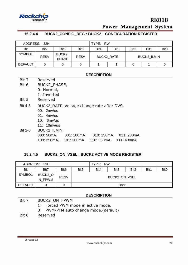
RK818 Power Management System
Version 0.3 www.rock-chips.com 70
BUCK2_CONFIG_REG : BUCK2 CONFIGURATION REGISTER 15.2.4.4
ADDRESS: 32H TYPE: RW
Bit Bit7 Bit6 Bit5 Bit4 Bit3 Bit2 Bit1 Bit0
SYMBOL RESV
BUCK2_
PHASE RESV BUCK2_RATE BUCK2_ILMIN
DEFAULT 0 0 0 1 1 0 1 0
DESCRIPTION
Bit 7 Reserved
Bit 6 BUCK2_PHASE,
0: Normal,
1: Inverted
Bit 5 Reserved
Bit 4-3 BUCK2_RATE: Voltage change rate after DVS.
00: 2mv/us
01: 4mv/us
10: 6mv/us
11: 10mv/us
Bit 2-0 BUCK2_ILMIN:
000: 50mA, 001: 100mA, 010: 150mA, 011: 200mA
100: 250mA, 101: 300mA, 110: 350mA, 111: 400mA
BUCK2_ON_VSEL : BUCK2 ACTIVE MODE REGISTER 15.2.4.5
ADDRESS: 33H TYPE: RW
Bit Bit7 Bit6 Bit5 Bit4 Bit3 Bit2 Bit1 Bit0
SYMBOL BUCK2_O
N_FPWM RESV BUCK2_ON_VSEL
DEFAULT 0 0 Boot
DESCRIPTION
Bit 7 BUCK2_ON_FPWM
1: Forced PWM mode in active mode.
0: PWM/PFM auto change mode.(default)
Bit 6 Reserved
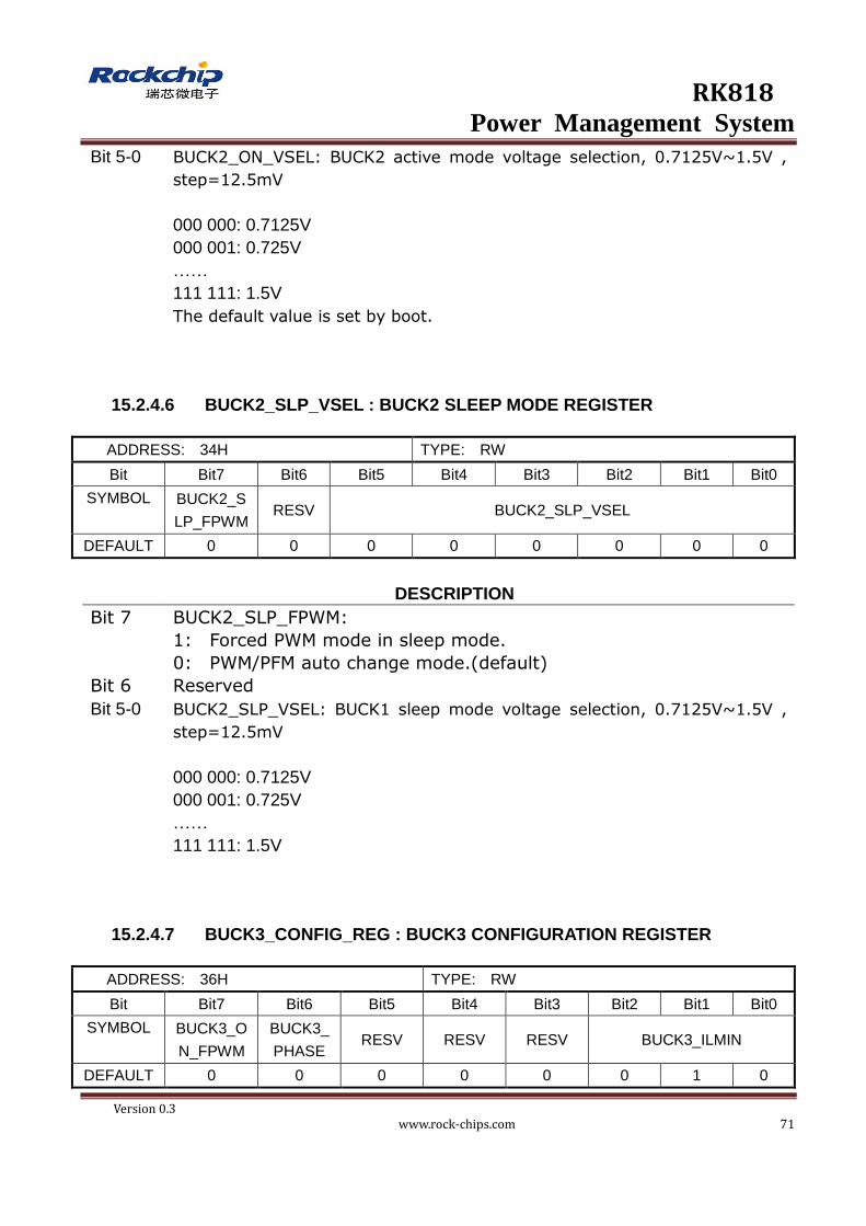
RK818 Power Management System
Version 0.3 www.rock-chips.com 71
Bit 5-0 BUCK2_ON_VSEL: BUCK2 active mode voltage selection, 0.7125V~1.5V ,
step=12.5mV
000 000: 0.7125V
000 001: 0.725V
……
111 111: 1.5V
The default value is set by boot.
BUCK2_SLP_VSEL : BUCK2 SLEEP MODE REGISTER 15.2.4.6
ADDRESS: 34H TYPE: RW
Bit Bit7 Bit6 Bit5 Bit4 Bit3 Bit2 Bit1 Bit0
SYMBOL BUCK2_S
LP_FPWM RESV BUCK2_SLP_VSEL
DEFAULT 0 0 0 0 0 0 0 0
DESCRIPTION
Bit 7 BUCK2_SLP_FPWM:
1: Forced PWM mode in sleep mode.
0: PWM/PFM auto change mode.(default)
Bit 6 Reserved
Bit 5-0 BUCK2_SLP_VSEL: BUCK1 sleep mode voltage selection, 0.7125V~1.5V ,
step=12.5mV
000 000: 0.7125V
000 001: 0.725V
……
111 111: 1.5V
BUCK3_CONFIG_REG : BUCK3 CONFIGURATION REGISTER 15.2.4.7
ADDRESS: 36H TYPE: RW
Bit Bit7 Bit6 Bit5 Bit4 Bit3 Bit2 Bit1 Bit0
SYMBOL BUCK3_O
N_FPWM
BUCK3_
PHASE RESV RESV RESV BUCK3_ILMIN
DEFAULT 0 0 0 0 0 0 1 0
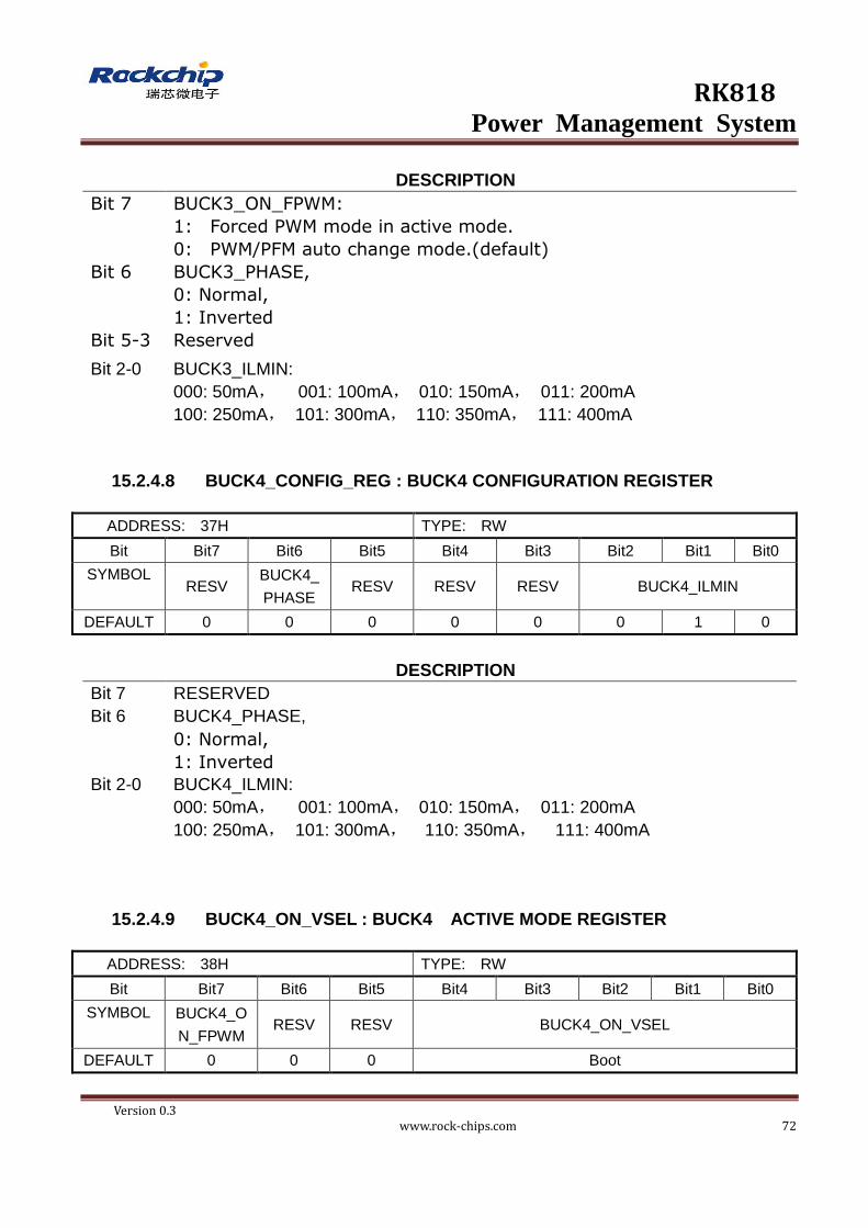
RK818 Power Management System
Version 0.3 www.rock-chips.com 72
DESCRIPTION
Bit 7 BUCK3_ON_FPWM:
1: Forced PWM mode in active mode.
0: PWM/PFM auto change mode.(default)
Bit 6 BUCK3_PHASE,
0: Normal,
1: Inverted
Bit 5-3 Reserved
Bit 2-0 BUCK3_ILMIN:
000: 50mA, 001: 100mA, 010: 150mA, 011: 200mA
100: 250mA, 101: 300mA, 110: 350mA, 111: 400mA
BUCK4_CONFIG_REG : BUCK4 CONFIGURATION REGISTER 15.2.4.8
ADDRESS: 37H TYPE: RW
Bit Bit7 Bit6 Bit5 Bit4 Bit3 Bit2 Bit1 Bit0
SYMBOL RESV
BUCK4_
PHASE RESV RESV RESV BUCK4_ILMIN
DEFAULT 0 0 0 0 0 0 1 0
DESCRIPTION
Bit 7 RESERVED
Bit 6 BUCK4_PHASE,
0: Normal,
1: Inverted
Bit 2-0 BUCK4_ILMIN:
000: 50mA, 001: 100mA, 010: 150mA, 011: 200mA
100: 250mA, 101: 300mA, 110: 350mA, 111: 400mA
BUCK4_ON_VSEL : BUCK4 ACTIVE MODE REGISTER 15.2.4.9
ADDRESS: 38H TYPE: RW
Bit Bit7 Bit6 Bit5 Bit4 Bit3 Bit2 Bit1 Bit0
SYMBOL BUCK4_O
N_FPWM RESV RESV BUCK4_ON_VSEL
DEFAULT 0 0 0 Boot
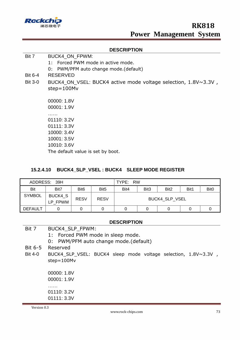
RK818 Power Management System
Version 0.3 www.rock-chips.com 73
DESCRIPTION
Bit 7 BUCK4_ON_FPWM:
1: Forced PWM mode in active mode.
0: PWM/PFM auto change mode.(default)
Bit 6-4 RESERVED
Bit 3-0 BUCK4_ON_VSEL: BUCK4 active mode voltage selection, 1.8V~3.3V ,
step=100Mv
00000: 1.8V
00001: 1.9V
……
01110: 3.2V
01111: 3.3V
10000: 3.4V
10001: 3.5V
10010: 3.6V
The default value is set by boot.
BUCK4_SLP_VSEL : BUCK4 SLEEP MODE REGISTER 15.2.4.10
ADDRESS: 39H TYPE: RW
Bit Bit7 Bit6 Bit5 Bit4 Bit3 Bit2 Bit1 Bit0
SYMBOL BUCK4_S
LP_FPWM RESV RESV BUCK4_SLP_VSEL
DEFAULT 0 0 0 0 0 0 0 0
DESCRIPTION
Bit 7 BUCK4_SLP_FPWM:
1: Forced PWM mode in sleep mode.
0: PWM/PFM auto change mode.(default)
Bit 6-5 Reserved
Bit 4-0 BUCK4_SLP_VSEL: BUCK4 sleep mode voltage selection, 1.8V~3.3V ,
step=100Mv
00000: 1.8V
00001: 1.9V
……
01110: 3.2V
01111: 3.3V
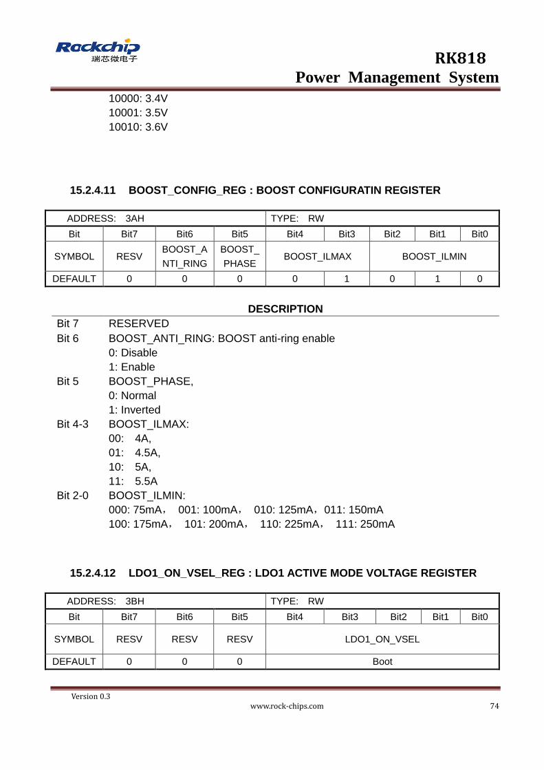
RK818 Power Management System
Version 0.3 www.rock-chips.com 74
10000: 3.4V
10001: 3.5V
10010: 3.6V
BOOST_CONFIG_REG : BOOST CONFIGURATIN REGISTER 15.2.4.11
ADDRESS: 3AH TYPE: RW
Bit Bit7 Bit6 Bit5 Bit4 Bit3 Bit2 Bit1 Bit0
SYMBOL RESV BOOST_A
NTI_RING
BOOST_
PHASE BOOST_ILMAX BOOST_ILMIN
DEFAULT 0 0 0 0 1 0 1 0
DESCRIPTION
Bit 7 RESERVED
Bit 6 BOOST_ANTI_RING: BOOST anti-ring enable
0: Disable
1: Enable
Bit 5 BOOST_PHASE,
0: Normal
1: Inverted
Bit 4-3 BOOST_ILMAX:
00: 4A,
01: 4.5A,
10: 5A,
11: 5.5A
Bit 2-0 BOOST_ILMIN:
000: 75mA, 001: 100mA, 010: 125mA,011: 150mA
100: 175mA, 101: 200mA, 110: 225mA, 111: 250mA
LDO1_ON_VSEL_REG : LDO1 ACTIVE MODE VOLTAGE REGISTER 15.2.4.12
ADDRESS: 3BH TYPE: RW
Bit Bit7 Bit6 Bit5 Bit4 Bit3 Bit2 Bit1 Bit0
SYMBOL RESV RESV RESV LDO1_ON_VSEL
DEFAULT 0 0 0 Boot
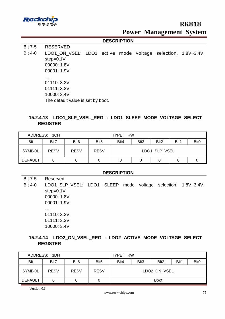
RK818 Power Management System
Version 0.3 www.rock-chips.com 75
DESCRIPTION
Bit 7-5 RESERVED
Bit 4-0 LDO1_ON_VSEL: LDO1 active mode voltage selection, 1.8V~3.4V,
step=0.1V
00000: 1.8V
00001: 1.9V
….
01110: 3.2V
01111: 3.3V
10000: 3.4V
The default value is set by boot.
LDO1_SLP_VSEL_REG : LDO1 SLEEP MODE VOLTAGE SELECT 15.2.4.13
REGISTER
ADDRESS: 3CH TYPE: RW
Bit Bit7 Bit6 Bit5 Bit4 Bit3 Bit2 Bit1 Bit0
SYMBOL RESV RESV RESV LDO1_SLP_VSEL
DEFAULT 0 0 0 0 0 0 0 0
DESCRIPTION
Bit 7-5 Reserved
Bit 4-0 LDO1_SLP_VSEL: LDO1 SLEEP mode voltage selection. 1.8V~3.4V,
step=0.1V
00000: 1.8V
00001: 1.9V
….
01110: 3.2V
01111: 3.3V
10000: 3.4V
LDO2_ON_VSEL_REG : LDO2 ACTIVE MODE VOLTAGE SELECT 15.2.4.14
REGISTER
ADDRESS: 3DH TYPE: RW
Bit Bit7 Bit6 Bit5 Bit4 Bit3 Bit2 Bit1 Bit0
SYMBOL RESV RESV RESV LDO2_ON_VSEL
DEFAULT 0 0 0 Boot

RK818 Power Management System
Version 0.3 www.rock-chips.com 76
DESCRIPTION
Bit 7-5 RESERVED
Bit 4-0 LDO2_ON_VSEL: LDO2 active mode voltage selection. 1.8V~3.4V, step=0.1V
00000: 1.8V
00001: 1.9V
….
01110: 3.2V
01111: 3.3V
10000: 3.4V
DEFAULT value is set by boot.
LDO2_SLP_VSEL_REG : LDO2 SLEEP MODE VOLTAGE SELECT 15.2.4.15
REGISTER
ADDRESS: 3EH TYPE: RW
Bit Bit7 Bit6 Bit5 Bit4 Bit3 Bit2 Bit1 Bit0
SYMBOL RESV RESV RESV LDO2_SLP_VSEL
DEFAULT 0 0 0 0 0 0 0 0
DESCRIPTION
Bit 7-5 RESERVED
Bit 4-0 LDO2_SLP_VSEL: LDO2 sleep mode voltage selection.
1.8V~3.4V, step=0.1V
00000: 1.8V
00001: 1.9V
….
01110: 3.2V
01111: 3.3V
10000: 3.4V
LDO3_ON_VSEL_REG : LDO3 ACTIVE MODE VOLTAGE SELECT 15.2.4.16
REGISTER
ADDRESS: 3FH TYPE: RW
Bit Bit7 Bit6 Bit5 Bit4 Bit3 Bit2 Bit1 Bit0
SYMBOL RESV RESV RESV RESV LDO3_ON_VSEL
DEFAULT 0 0 0 0 Boot
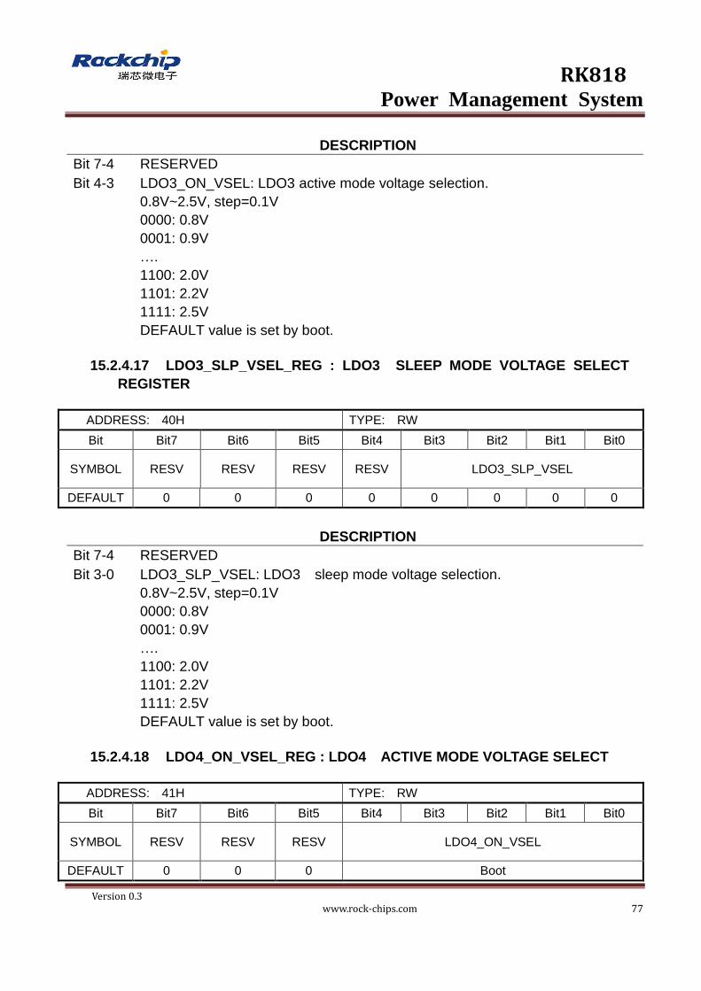
RK818 Power Management System
Version 0.3 www.rock-chips.com 77
DESCRIPTION
Bit 7-4 RESERVED
Bit 4-3 LDO3_ON_VSEL: LDO3 active mode voltage selection.
0.8V~2.5V, step=0.1V
0000: 0.8V
0001: 0.9V
….
1100: 2.0V
1101: 2.2V
1111: 2.5V
DEFAULT value is set by boot.
LDO3_SLP_VSEL_REG : LDO3 SLEEP MODE VOLTAGE SELECT 15.2.4.17
REGISTER
ADDRESS: 40H TYPE: RW
Bit Bit7 Bit6 Bit5 Bit4 Bit3 Bit2 Bit1 Bit0
SYMBOL RESV RESV RESV RESV LDO3_SLP_VSEL
DEFAULT 0 0 0 0 0 0 0 0
DESCRIPTION
Bit 7-4 RESERVED
Bit 3-0 LDO3_SLP_VSEL: LDO3 sleep mode voltage selection.
0.8V~2.5V, step=0.1V
0000: 0.8V
0001: 0.9V
….
1100: 2.0V
1101: 2.2V
1111: 2.5V
DEFAULT value is set by boot.
LDO4_ON_VSEL_REG : LDO4 ACTIVE MODE VOLTAGE SELECT 15.2.4.18
ADDRESS: 41H TYPE: RW
Bit Bit7 Bit6 Bit5 Bit4 Bit3 Bit2 Bit1 Bit0
SYMBOL RESV RESV RESV LDO4_ON_VSEL
DEFAULT 0 0 0 Boot
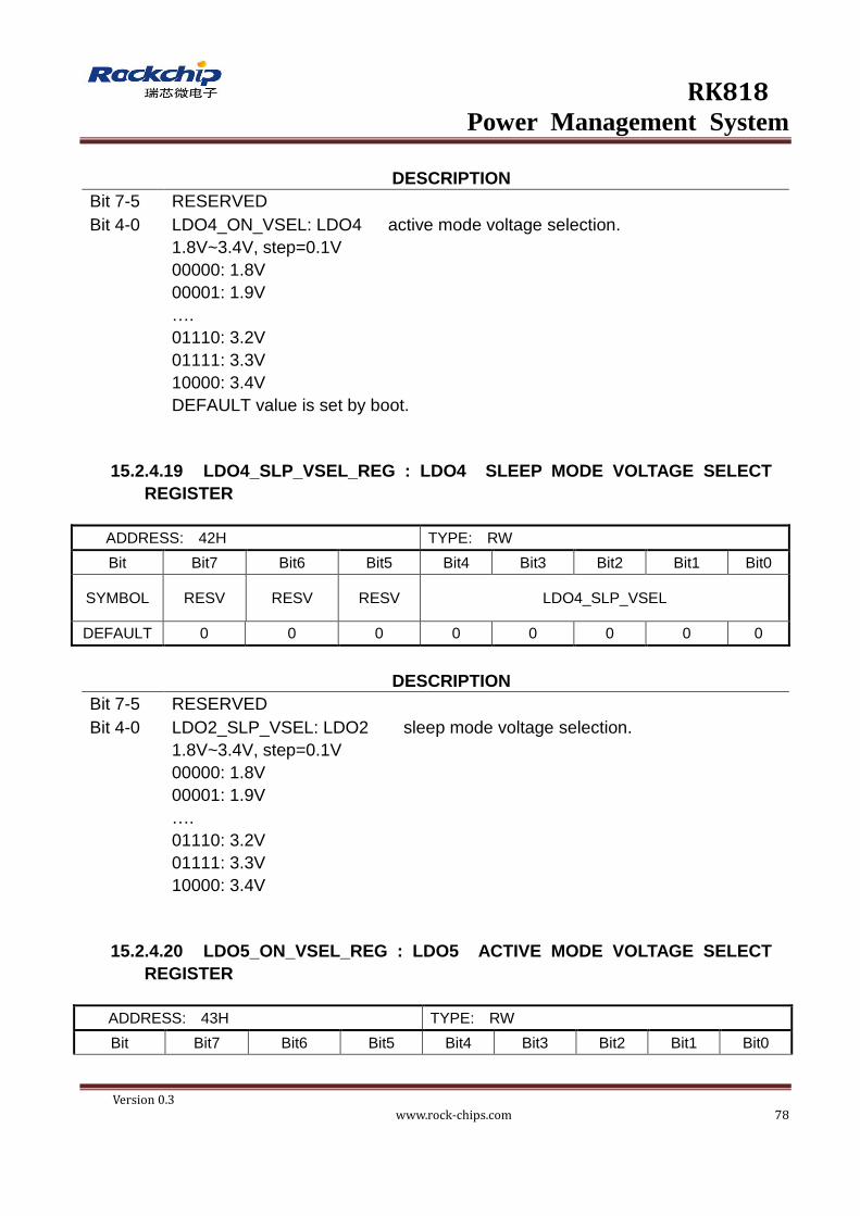
RK818 Power Management System
Version 0.3 www.rock-chips.com 78
DESCRIPTION
Bit 7-5 RESERVED
Bit 4-0 LDO4_ON_VSEL: LDO4 active mode voltage selection.
1.8V~3.4V, step=0.1V
00000: 1.8V
00001: 1.9V
….
01110: 3.2V
01111: 3.3V
10000: 3.4V
DEFAULT value is set by boot.
LDO4_SLP_VSEL_REG : LDO4 SLEEP MODE VOLTAGE SELECT 15.2.4.19
REGISTER
ADDRESS: 42H TYPE: RW
Bit Bit7 Bit6 Bit5 Bit4 Bit3 Bit2 Bit1 Bit0
SYMBOL RESV RESV RESV LDO4_SLP_VSEL
DEFAULT 0 0 0 0 0 0 0 0
DESCRIPTION
Bit 7-5 RESERVED
Bit 4-0 LDO2_SLP_VSEL: LDO2 sleep mode voltage selection.
1.8V~3.4V, step=0.1V
00000: 1.8V
00001: 1.9V
….
01110: 3.2V
01111: 3.3V
10000: 3.4V
LDO5_ON_VSEL_REG : LDO5 ACTIVE MODE VOLTAGE SELECT 15.2.4.20
REGISTER
ADDRESS: 43H TYPE: RW
Bit Bit7 Bit6 Bit5 Bit4 Bit3 Bit2 Bit1 Bit0
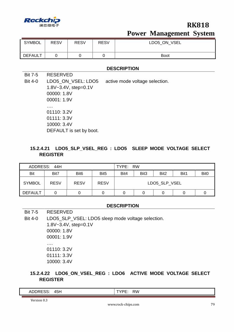
RK818 Power Management System
Version 0.3 www.rock-chips.com 79
SYMBOL RESV RESV RESV LDO5_ON_VSEL
DEFAULT 0 0 0 Boot
DESCRIPTION
Bit 7-5 RESERVED
Bit 4-0 LDO5_ON_VSEL: LDO5 active mode voltage selection.
1.8V~3.4V, step=0.1V
00000: 1.8V
00001: 1.9V
….
01110: 3.2V
01111: 3.3V
10000: 3.4V
DEFAULT is set by boot.
LDO5_SLP_VSEL_REG : LDO5 SLEEP MODE VOLTAGE SELECT 15.2.4.21
REGISTER
ADDRESS: 44H TYPE: RW
Bit Bit7 Bit6 Bit5 Bit4 Bit3 Bit2 Bit1 Bit0
SYMBOL RESV RESV RESV LDO5_SLP_VSEL
DEFAULT 0 0 0 0 0 0 0 0
DESCRIPTION
Bit 7-5 RESERVED
Bit 4-0 LDO5_SLP_VSEL: LDO5 sleep mode voltage selection.
1.8V~3.4V, step=0.1V
00000: 1.8V
00001: 1.9V
….
01110: 3.2V
01111: 3.3V
10000: 3.4V
LDO6_ON_VSEL_REG : LDO6 ACTIVE MODE VOLTAGE SELECT 15.2.4.22
REGISTER
ADDRESS: 45H TYPE: RW
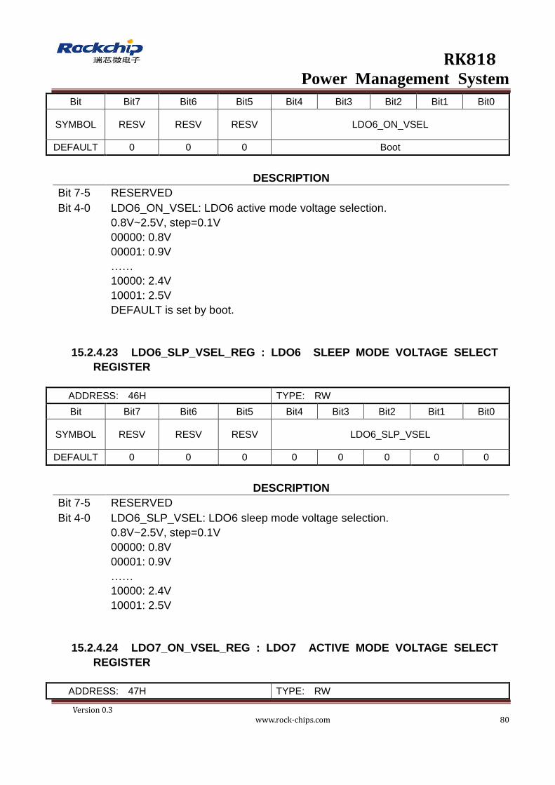
RK818 Power Management System
Version 0.3 www.rock-chips.com 80
Bit Bit7 Bit6 Bit5 Bit4 Bit3 Bit2 Bit1 Bit0
SYMBOL RESV RESV RESV LDO6_ON_VSEL
DEFAULT 0 0 0 Boot
DESCRIPTION
Bit 7-5 RESERVED
Bit 4-0 LDO6_ON_VSEL: LDO6 active mode voltage selection.
0.8V~2.5V, step=0.1V
00000: 0.8V
00001: 0.9V
……
10000: 2.4V
10001: 2.5V
DEFAULT is set by boot.
LDO6_SLP_VSEL_REG : LDO6 SLEEP MODE VOLTAGE SELECT 15.2.4.23
REGISTER
ADDRESS: 46H TYPE: RW
Bit Bit7 Bit6 Bit5 Bit4 Bit3 Bit2 Bit1 Bit0
SYMBOL RESV RESV RESV LDO6_SLP_VSEL
DEFAULT 0 0 0 0 0 0 0 0
DESCRIPTION
Bit 7-5 RESERVED
Bit 4-0 LDO6_SLP_VSEL: LDO6 sleep mode voltage selection.
0.8V~2.5V, step=0.1V
00000: 0.8V
00001: 0.9V
……
10000: 2.4V
10001: 2.5V
LDO7_ON_VSEL_REG : LDO7 ACTIVE MODE VOLTAGE SELECT 15.2.4.24
REGISTER
ADDRESS: 47H TYPE: RW
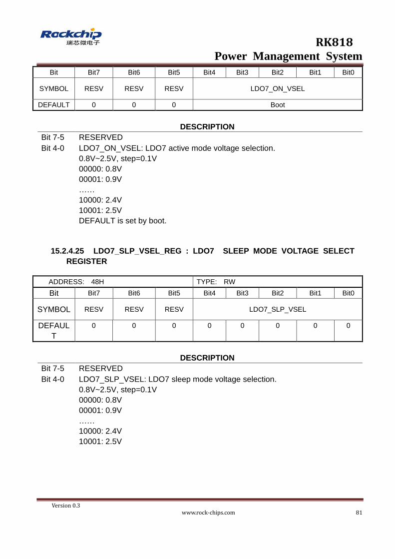
RK818 Power Management System
Version 0.3 www.rock-chips.com 81
Bit Bit7 Bit6 Bit5 Bit4 Bit3 Bit2 Bit1 Bit0
SYMBOL RESV RESV RESV LDO7_ON_VSEL
DEFAULT 0 0 0 Boot
DESCRIPTION
Bit 7-5 RESERVED
Bit 4-0 LDO7_ON_VSEL: LDO7 active mode voltage selection.
0.8V~2.5V, step=0.1V
00000: 0.8V
00001: 0.9V
……
10000: 2.4V
10001: 2.5V
DEFAULT is set by boot.
LDO7_SLP_VSEL_REG : LDO7 SLEEP MODE VOLTAGE SELECT 15.2.4.25
REGISTER
ADDRESS: 48H TYPE: RW
Bit Bit7 Bit6 Bit5 Bit4 Bit3 Bit2 Bit1 Bit0
SYMBOL RESV RESV RESV LDO7_SLP_VSEL
DEFAUL
T
0 0 0 0 0 0 0 0
DESCRIPTION
Bit 7-5 RESERVED
Bit 4-0 LDO7_SLP_VSEL: LDO7 sleep mode voltage selection.
0.8V~2.5V, step=0.1V
00000: 0.8V
00001: 0.9V
……
10000: 2.4V
10001: 2.5V
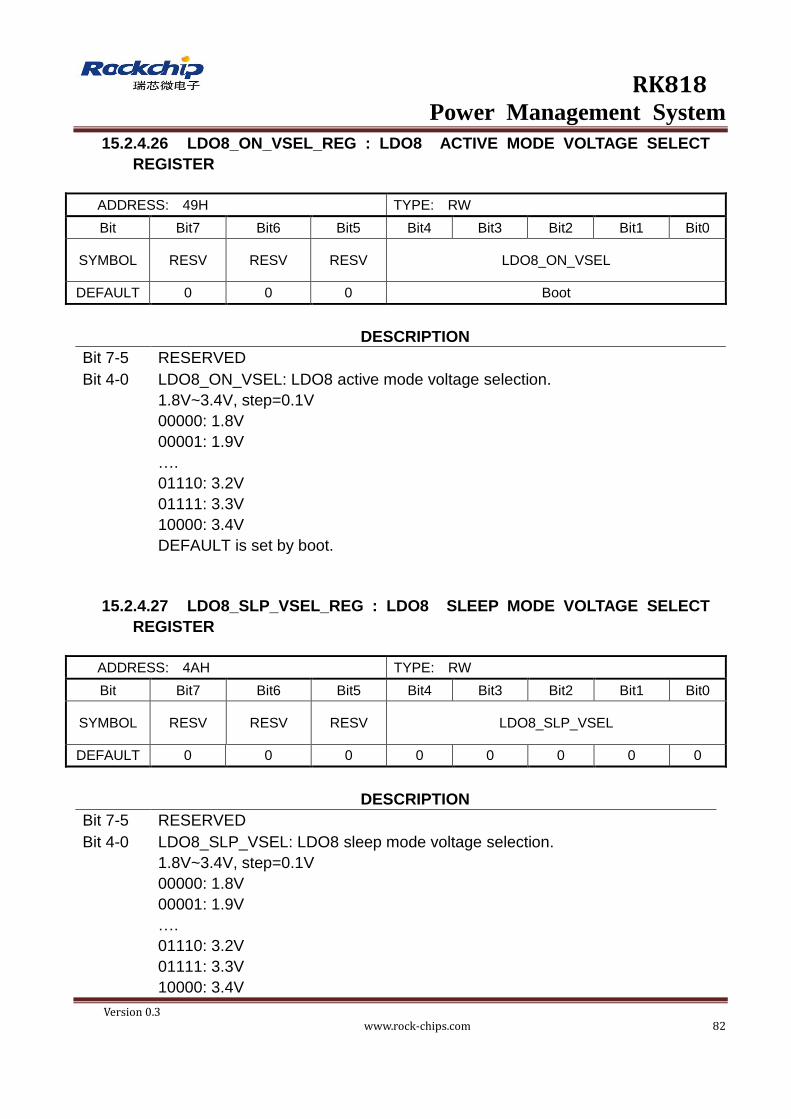
RK818 Power Management System
Version 0.3 www.rock-chips.com 82
LDO8_ON_VSEL_REG : LDO8 ACTIVE MODE VOLTAGE SELECT 15.2.4.26
REGISTER
ADDRESS: 49H TYPE: RW
Bit Bit7 Bit6 Bit5 Bit4 Bit3 Bit2 Bit1 Bit0
SYMBOL RESV RESV RESV LDO8_ON_VSEL
DEFAULT 0 0 0 Boot
DESCRIPTION
Bit 7-5 RESERVED
Bit 4-0 LDO8_ON_VSEL: LDO8 active mode voltage selection.
1.8V~3.4V, step=0.1V
00000: 1.8V
00001: 1.9V
….
01110: 3.2V
01111: 3.3V
10000: 3.4V
DEFAULT is set by boot.
LDO8_SLP_VSEL_REG : LDO8 SLEEP MODE VOLTAGE SELECT 15.2.4.27
REGISTER
ADDRESS: 4AH TYPE: RW
Bit Bit7 Bit6 Bit5 Bit4 Bit3 Bit2 Bit1 Bit0
SYMBOL RESV RESV RESV LDO8_SLP_VSEL
DEFAULT 0 0 0 0 0 0 0 0
DESCRIPTION
Bit 7-5 RESERVED
Bit 4-0 LDO8_SLP_VSEL: LDO8 sleep mode voltage selection.
1.8V~3.4V, step=0.1V
00000: 1.8V
00001: 1.9V
….
01110: 3.2V
01111: 3.3V
10000: 3.4V
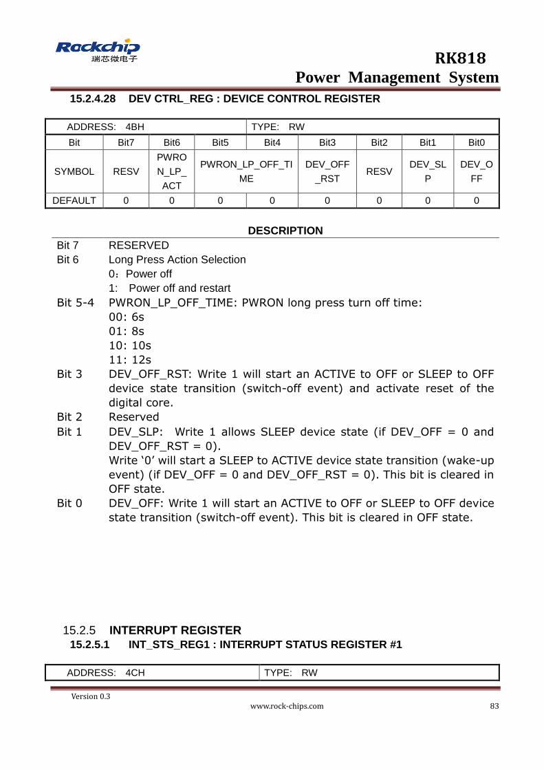
RK818 Power Management System
Version 0.3 www.rock-chips.com 83
DEV CTRL_REG : DEVICE CONTROL REGISTER 15.2.4.28
ADDRESS: 4BH TYPE: RW
Bit Bit7 Bit6 Bit5 Bit4 Bit3 Bit2 Bit1 Bit0
SYMBOL RESV
PWRO
N_LP_
ACT
PWRON_LP_OFF_TI
ME
DEV_OFF
_RST RESV
DEV_SL
P
DEV_O
FF
DEFAULT 0 0 0 0 0 0 0 0
DESCRIPTION
Bit 7
Bit 6
RESERVED
Long Press Action Selection
0:Power off
1: Power off and restart
Bit 5-4 PWRON_LP_OFF_TIME: PWRON long press turn off time:
00: 6s
01: 8s
10: 10s
11: 12s
Bit 3 DEV_OFF_RST: Write 1 will start an ACTIVE to OFF or SLEEP to OFF
device state transition (switch-off event) and activate reset of the
digital core.
Bit 2 Reserved
Bit 1 DEV_SLP: Write 1 allows SLEEP device state (if DEV_OFF = 0 and
DEV_OFF_RST = 0).
Write ‘0’ will start a SLEEP to ACTIVE device state transition (wake-up
event) (if DEV_OFF = 0 and DEV_OFF_RST = 0). This bit is cleared in
OFF state.
Bit 0 DEV_OFF: Write 1 will start an ACTIVE to OFF or SLEEP to OFF device
state transition (switch-off event). This bit is cleared in OFF state.
INTERRUPT REGISTER 15.2.5
INT_STS_REG1 : INTERRUPT STATUS REGISTER #1 15.2.5.1
ADDRESS: 4CH TYPE: RW
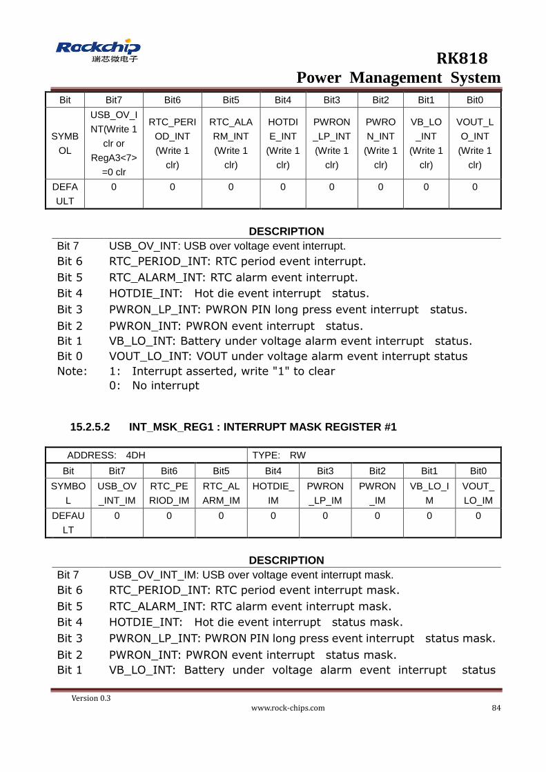
RK818 Power Management System
Version 0.3 www.rock-chips.com 84
Bit Bit7 Bit6 Bit5 Bit4 Bit3 Bit2 Bit1 Bit0
SYMB
OL
USB_OV_I
NT(Write 1
clr or
RegA3<7>
=0 clr
RTC_PERI
OD_INT
(Write 1
clr)
RTC_ALA
RM_INT
(Write 1
clr)
HOTDI
E_INT
(Write 1
clr)
PWRON
_LP_INT
(Write 1
clr)
PWRO
N_INT
(Write 1
clr)
VB_LO
_INT
(Write 1
clr)
VOUT_L
O_INT
(Write 1
clr)
DEFA
ULT
0 0 0 0 0 0 0 0
DESCRIPTION
Bit 7 USB_OV_INT: USB over voltage event interrupt.
Bit 6 RTC_PERIOD_INT: RTC period event interrupt.
Bit 5 RTC_ALARM_INT: RTC alarm event interrupt.
Bit 4 HOTDIE_INT: Hot die event interrupt status.
Bit 3 PWRON_LP_INT: PWRON PIN long press event interrupt status.
Bit 2 PWRON_INT: PWRON event interrupt status.
Bit 1 VB_LO_INT: Battery under voltage alarm event interrupt status.
Bit 0 VOUT_LO_INT: VOUT under voltage alarm event interrupt status
Note: 1: Interrupt asserted, write "1" to clear
0: No interrupt
INT_MSK_REG1 : INTERRUPT MASK REGISTER #1 15.2.5.2
ADDRESS: 4DH TYPE: RW
Bit Bit7 Bit6 Bit5 Bit4 Bit3 Bit2 Bit1 Bit0
SYMBO
L
USB_OV
_INT_IM
RTC_PE
RIOD_IM
RTC_AL
ARM_IM
HOTDIE_
IM
PWRON
_LP_IM
PWRON
_IM
VB_LO_I
M
VOUT_
LO_IM
DEFAU
LT
0 0 0 0 0 0 0 0
DESCRIPTION
Bit 7 USB_OV_INT_IM: USB over voltage event interrupt mask.
Bit 6 RTC_PERIOD_INT: RTC period event interrupt mask.
Bit 5 RTC_ALARM_INT: RTC alarm event interrupt mask.
Bit 4 HOTDIE_INT: Hot die event interrupt status mask.
Bit 3 PWRON_LP_INT: PWRON PIN long press event interrupt status mask.
Bit 2 PWRON_INT: PWRON event interrupt status mask.
Bit 1 VB_LO_INT: Battery under voltage alarm event interrupt status
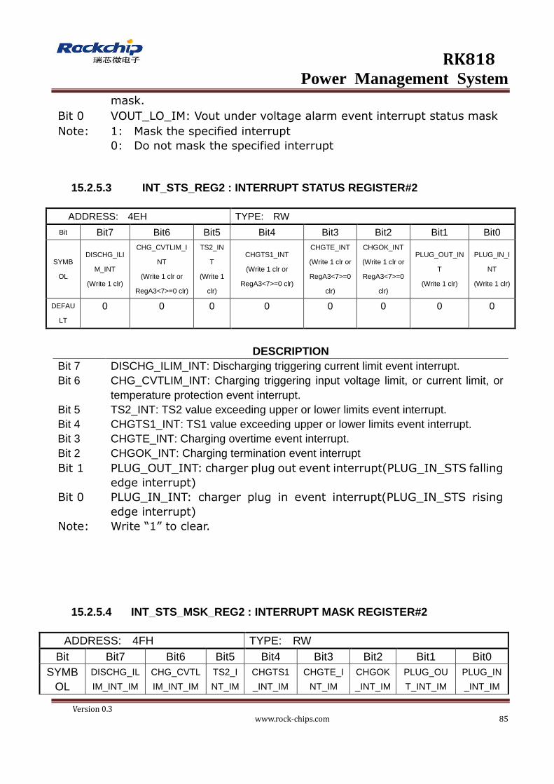
RK818 Power Management System
Version 0.3 www.rock-chips.com 85
mask.
Bit 0 VOUT_LO_IM: Vout under voltage alarm event interrupt status mask
Note: 1: Mask the specified interrupt
0: Do not mask the specified interrupt
INT_STS_REG2 : INTERRUPT STATUS REGISTER#2 15.2.5.3
ADDRESS: 4EH TYPE: RW
Bit Bit7 Bit6 Bit5 Bit4 Bit3 Bit2 Bit1 Bit0
SYMB
OL
DISCHG_ILI
M_INT
(Write 1 clr)
CHG_CVTLIM_I
NT
(Write 1 clr or
RegA3<7>=0 clr)
TS2_IN
T
(Write 1
clr)
CHGTS1_INT
(Write 1 clr or
RegA3<7>=0 clr)
CHGTE_INT
(Write 1 clr or
RegA3<7>=0
clr)
CHGOK_INT
(Write 1 clr or
RegA3<7>=0
clr)
PLUG_OUT_IN
T
(Write 1 clr)
PLUG_IN_I
NT
(Write 1 clr)
DEFAU
LT
0 0 0 0 0 0 0 0
DESCRIPTION
Bit 7
Bit 6
Bit 5
Bit 4
Bit 3
Bit 2
DISCHG_ILIM_INT: Discharging triggering current limit event interrupt.
CHG_CVTLIM_INT: Charging triggering input voltage limit, or current limit, or
temperature protection event interrupt.
TS2_INT: TS2 value exceeding upper or lower limits event interrupt.
CHGTS1_INT: TS1 value exceeding upper or lower limits event interrupt.
CHGTE_INT: Charging overtime event interrupt.
CHGOK_INT: Charging termination event interrupt
Bit 1 PLUG_OUT_INT: charger plug out event interrupt(PLUG_IN_STS falling
edge interrupt)
Bit 0 PLUG_IN_INT: charger plug in event interrupt(PLUG_IN_STS rising
edge interrupt)
Note: Write “1” to clear.
INT_STS_MSK_REG2 : INTERRUPT MASK REGISTER#2 15.2.5.4
ADDRESS: 4FH TYPE: RW
Bit Bit7 Bit6 Bit5 Bit4 Bit3 Bit2 Bit1 Bit0
SYMB
OL
DISCHG_IL
IM_INT_IM
CHG_CVTL
IM_INT_IM
TS2_I
NT_IM
CHGTS1
_INT_IM
CHGTE_I
NT_IM
CHGOK
_INT_IM
PLUG_OU
T_INT_IM
PLUG_IN
_INT_IM
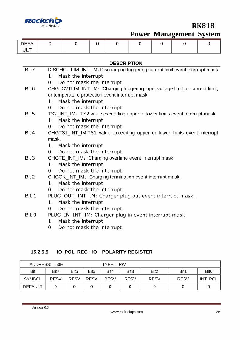
RK818 Power Management System
Version 0.3 www.rock-chips.com 86
DEFA
ULT
0 0 0 0 0 0 0 0
DESCRIPTION
Bit 7
Bit 6
Bit 5
Bit 4
Bit 3
Bit 2
DISCHG_ILIM_INT_IM:Discharging triggering current limit event interrupt mask
1: Mask the interrupt
0: Do not mask the interrupt
CHG_CVTLIM_INT_IM:Charging triggering input voltage limit, or current limit,
or temperature protection event interrupt mask.
1: Mask the interrupt
0: Do not mask the interrupt
TS2_INT_IM:TS2 value exceeding upper or lower limits event interrupt mask
1: Mask the interrupt
0: Do not mask the interrupt
CHGTS1_INT_IM:TS1 value exceeding upper or lower limits event interrupt
mask.
1: Mask the interrupt
0: Do not mask the interrupt
CHGTE_INT_IM:Charging overtime event interrupt mask
1: Mask the interrupt
0: Do not mask the interrupt
CHGOK_INT_IM:Charging termination event interrupt mask.
1: Mask the interrupt
0: Do not mask the interrupt
Bit 1 PLUG_OUT_INT_IM: Charger plug out event interrupt mask.
1: Mask the interrupt
0: Do not mask the interrupt
Bit 0 PLUG_IN_INT_IM: Charger plug in event interrupt mask
1: Mask the interrupt
0: Do not mask the interrupt
IO_POL_REG : IO POLARITY REGISTER 15.2.5.5
ADDRESS: 50H TYPE: RW
Bit Bit7 Bit6 Bit5 Bit4 Bit3 Bit2 Bit1 Bit0
SYMBOL RESV RESV RESV RESV RESV RESV RESV INT_POL
DEFAULT 0 0 0 0 0 0 0 0
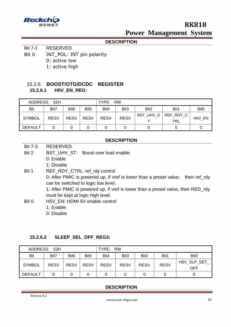
RK818 Power Management System
Version 0.3 www.rock-chips.com 87
DESCRIPTION
Bit 7-1 RESERVED
Bit 0 INT_POL: INT pin polarity
0: active low
1: active high
BOOST/OTG/DCDC REGISTER 15.2.6
H5V_EN_REG: 15.2.6.1
ADDRESS: 52H TYPE: RW
Bit Bit7 Bit6 Bit5 Bit4 Bit3 Bit2 Bit1 Bit0
SYMBOL RESV RESV RESV RESV RESV BST_UHV_S
T
REF_RDY_C
TRL H5V_EN
DEFAULT 0 0 0 0 0 0 0 0
DESCRIPTION
Bit 7-3 RESERVED
Bit 2 BST_UHV_ST: Boost over load enable
0: Enable
1: Disable
Bit 1 REF_RDY_CTRL: ref_rdy control
0: After PMIC is powered up, if vref is lower than a preset value, then ref_rdy
can be switched to logic low level.
1: After PMIC is powered up, if vref is lower than a preset value, then RED_rdy
must be kept at logic high level.
Bit 0 H5V_EN: HDMI 5V enable control
1: Enable
0: Disable
SLEEP_SEL_OFF_REG3: 15.2.6.2
ADDRESS: 53H TYPE: RW
Bit Bit7 Bit6 Bit5 Bit4 Bit3 Bit2 Bit1 Bit0
SYMBOL RESV RESV RESV RESV RESV RESV RESV H5V_SLP_SET_
OFF
DEFAULT 0 0 0 0 0 0 0 0
DESCRIPTION
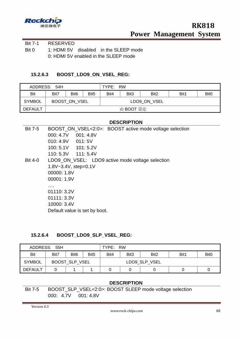
RK818 Power Management System
Version 0.3 www.rock-chips.com 88
Bit 7-1 RESERVED
Bit 0 1: HDMI 5V disabled in the SLEEP mode
0: HDMI 5V enabled in the SLEEP mode
BOOST_LDO9_ON_VSEL_REG: 15.2.6.3
ADDRESS: 54H TYPE: RW
Bit Bit7 Bit6 Bit5 Bit4 Bit3 Bit2 Bit1 Bit0
SYMBOL BOOST_ON_VSEL LDO9_ON_VSEL
DEFAULT 由 BOOT 设定
DESCRIPTION
Bit 7-5 BOOST_ON_VSEL<2:0>: BOOST active mode voltage selection
000: 4.7V 001: 4.8V
010: 4.9V 011: 5V
100: 5.1V 101: 5.2V
110: 5.3V 111: 5.4V
Bit 4-0 LDO9_ON_VSEL: LDO9 active mode voltage selection
1.8V~3.4V, step=0.1V
00000: 1.8V
00001: 1.9V
….
01110: 3.2V
01111: 3.3V
10000: 3.4V
Default value is set by boot.
BOOST_LDO9_SLP_VSEL_REG: 15.2.6.4
ADDRESS: 55H TYPE: RW
Bit Bit7 Bit6 Bit5 Bit4 Bit3 Bit2 Bit1 Bit0
SYMBOL BOOST_SLP_VSEL LDO9_SLP_VSEL
DEFAULT 0 1 1 0 0 0 0 0
DESCRIPTION
Bit 7-5 BOOST_SLP_VSEL<2:0>: BOOST SLEEP mode voltage selection
000: 4.7V 001: 4.8V
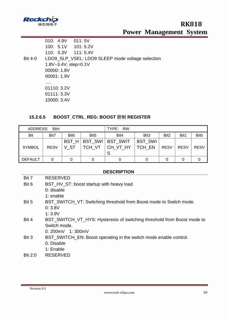
RK818 Power Management System
Version 0.3 www.rock-chips.com 89
010: 4.9V 011: 5V
100: 5.1V 101: 5.2V
110: 5.3V 111: 5.4V
Bit 4-0 LDO9_SLP_VSEL: LDO9 SLEEP mode voltage selection
1.8V~3.4V, step=0.1V
00000: 1.8V
00001: 1.9V
….
01110: 3.2V
01111: 3.3V
10000: 3.4V
BOOST_CTRL_REG: BOOST 控制 REGISTER 15.2.6.5
ADDRESS: 56H TYPE: RW
Bit Bit7 Bit6 Bit5 Bit4 Bit3 Bit2 Bit1 Bit0
SYMBOL RESV
BST_H
V_ST
BST_SWI
TCH_VT
BST_SWIT
CH_VT_HY
S
BST_SWI
TCH_EN RESV RESV RESV
DEFAULT 0 0 0 0 0 0 0 0
DESCRIPTION
Bit 7 RESERVED
Bit 6 BST_HV_ST: boost startup with heavy load
0: disable
1: enable
Bit 5 BST_SWITCH_VT: Switching threshold from Boost mode to Switch mode.
0: 3.8V
1: 3.9V
Bit 4 BST_SWITCH_VT_HYS: Hysteresis of switching threshold from Boost mode to
Switch mode.
0: 200mV 1: 300mV
Bit 3 BST_SWITCH_EN: Boost operating in the switch mode enable control.
0: Disable
1: Enable
Bit 2:0 RESERVED
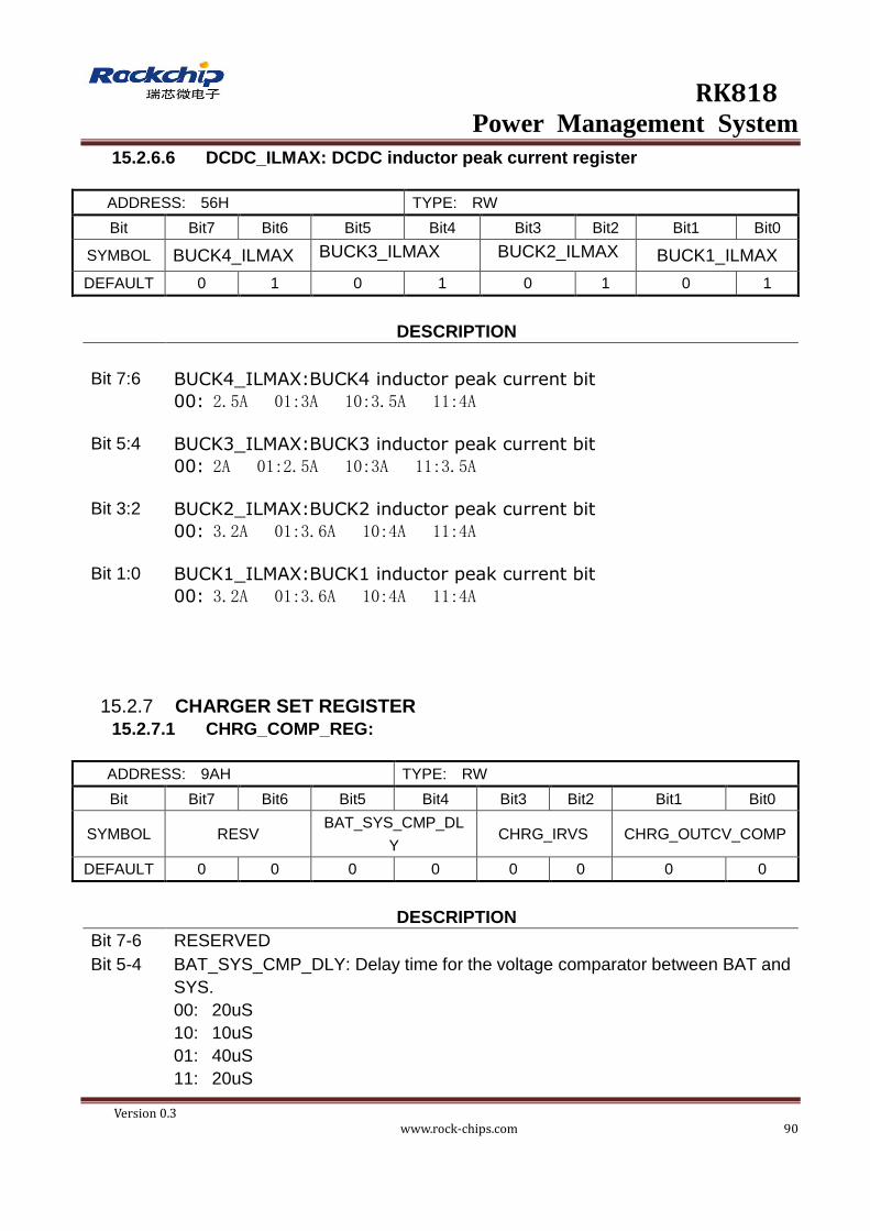
RK818 Power Management System
Version 0.3 www.rock-chips.com 90
DCDC_ILMAX: DCDC inductor peak current register 15.2.6.6
ADDRESS: 56H TYPE: RW
Bit Bit7 Bit6 Bit5 Bit4 Bit3 Bit2 Bit1 Bit0
SYMBOL BUCK4_ILMAX BUCK3_ILMAX BUCK2_ILMAX BUCK1_ILMAX
DEFAULT 0 1 0 1 0 1 0 1
DESCRIPTION
Bit 7:6 BUCK4_ILMAX:BUCK4 inductor peak current bit
00: 2.5A 01:3A 10:3.5A 11:4A
Bit 5:4 BUCK3_ILMAX:BUCK3 inductor peak current bit
00: 2A 01:2.5A 10:3A 11:3.5A
Bit 3:2 BUCK2_ILMAX:BUCK2 inductor peak current bit
00: 3.2A 01:3.6A 10:4A 11:4A
Bit 1:0 BUCK1_ILMAX:BUCK1 inductor peak current bit
00: 3.2A 01:3.6A 10:4A 11:4A
CHARGER SET REGISTER 15.2.7
CHRG_COMP_REG: 15.2.7.1
ADDRESS: 9AH TYPE: RW
Bit Bit7 Bit6 Bit5 Bit4 Bit3 Bit2 Bit1 Bit0
SYMBOL RESV BAT_SYS_CMP_DL
Y CHRG_IRVS CHRG_OUTCV_COMP
DEFAULT 0 0 0 0 0 0 0 0
DESCRIPTION
Bit 7-6 RESERVED
Bit 5-4 BAT_SYS_CMP_DLY: Delay time for the voltage comparator between BAT and
SYS.
00: 20uS
10: 10uS
01: 40uS
11: 20uS
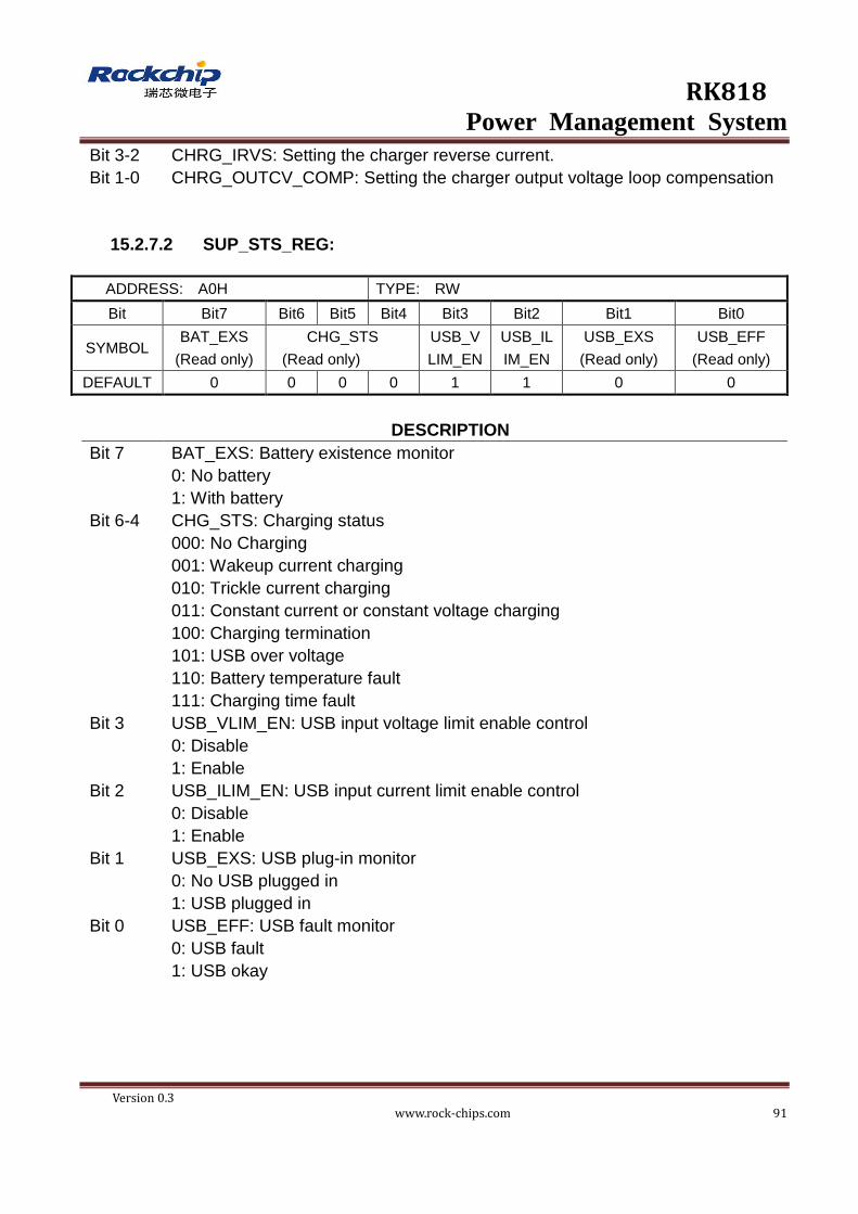
RK818 Power Management System
Version 0.3 www.rock-chips.com 91
Bit 3-2 CHRG_IRVS: Setting the charger reverse current.
Bit 1-0 CHRG_OUTCV_COMP: Setting the charger output voltage loop compensation
SUP_STS_REG: 15.2.7.2
ADDRESS: A0H TYPE: RW
Bit Bit7 Bit6 Bit5 Bit4 Bit3 Bit2 Bit1 Bit0
SYMBOL BAT_EXS
(Read only)
CHG_STS
(Read only)
USB_V
LIM_EN
USB_IL
IM_EN
USB_EXS
(Read only)
USB_EFF
(Read only)
DEFAULT 0 0 0 0 1 1 0 0
DESCRIPTION
Bit 7 BAT_EXS: Battery existence monitor
0: No battery
1: With battery
Bit 6-4 CHG_STS: Charging status
000: No Charging
001: Wakeup current charging
010: Trickle current charging
011: Constant current or constant voltage charging
100: Charging termination
101: USB over voltage
110: Battery temperature fault
111: Charging time fault
Bit 3 USB_VLIM_EN: USB input voltage limit enable control
0: Disable
1: Enable
Bit 2 USB_ILIM_EN: USB input current limit enable control
0: Disable
1: Enable
Bit 1 USB_EXS: USB plug-in monitor
0: No USB plugged in
1: USB plugged in
Bit 0 USB_EFF: USB fault monitor
0: USB fault
1: USB okay
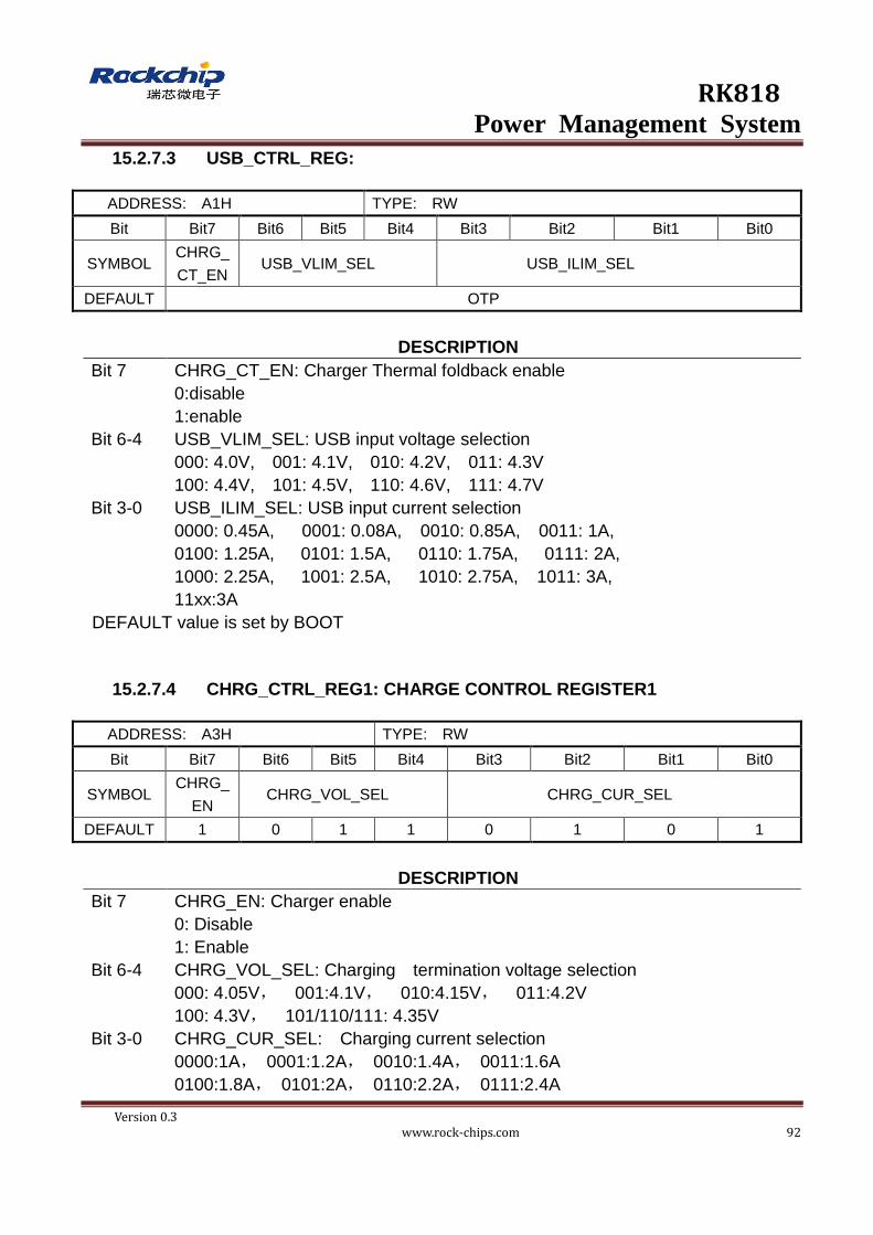
RK818 Power Management System
Version 0.3 www.rock-chips.com 92
USB_CTRL_REG: 15.2.7.3
ADDRESS: A1H TYPE: RW
Bit Bit7 Bit6 Bit5 Bit4 Bit3 Bit2 Bit1 Bit0
SYMBOL CHRG_
CT_EN USB_VLIM_SEL USB_ILIM_SEL
DEFAULT OTP
DESCRIPTION
Bit 7 CHRG_CT_EN: Charger Thermal foldback enable
0:disable
1:enable
Bit 6-4 USB_VLIM_SEL: USB input voltage selection
000: 4.0V, 001: 4.1V, 010: 4.2V, 011: 4.3V
100: 4.4V, 101: 4.5V, 110: 4.6V, 111: 4.7V
Bit 3-0 USB_ILIM_SEL: USB input current selection
0000: 0.45A, 0001: 0.08A, 0010: 0.85A, 0011: 1A,
0100: 1.25A, 0101: 1.5A, 0110: 1.75A, 0111: 2A,
1000: 2.25A, 1001: 2.5A, 1010: 2.75A, 1011: 3A,
11xx:3A
DEFAULT value is set by BOOT
CHRG_CTRL_REG1: CHARGE CONTROL REGISTER1 15.2.7.4
ADDRESS: A3H TYPE: RW
Bit Bit7 Bit6 Bit5 Bit4 Bit3 Bit2 Bit1 Bit0
SYMBOL CHRG_
EN CHRG_VOL_SEL CHRG_CUR_SEL
DEFAULT 1 0 1 1 0 1 0 1
DESCRIPTION
Bit 7 CHRG_EN: Charger enable
0: Disable
1: Enable
Bit 6-4 CHRG_VOL_SEL: Charging termination voltage selection
000: 4.05V, 001:4.1V, 010:4.15V, 011:4.2V
100: 4.3V, 101/110/111: 4.35V
Bit 3-0 CHRG_CUR_SEL: Charging current selection
0000:1A, 0001:1.2A, 0010:1.4A, 0011:1.6A
0100:1.8A, 0101:2A, 0110:2.2A, 0111:2.4A
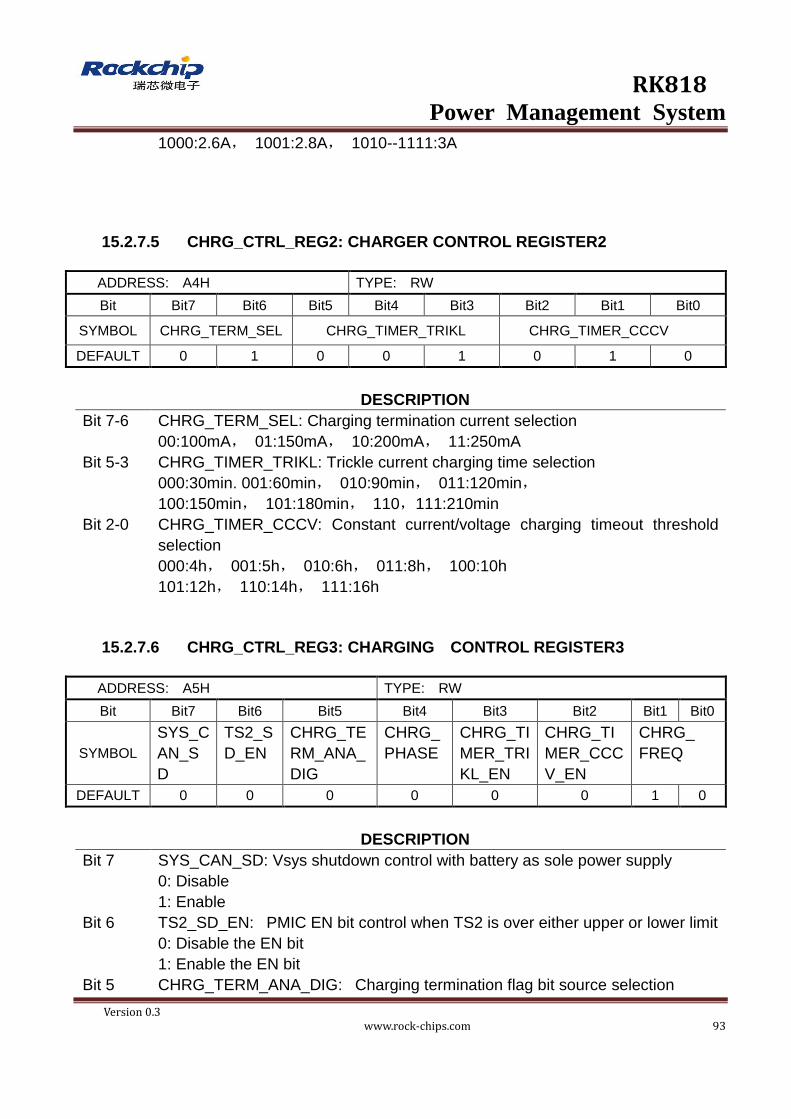
RK818 Power Management System
Version 0.3 www.rock-chips.com 93
1000:2.6A, 1001:2.8A, 1010--1111:3A
CHRG_CTRL_REG2: CHARGER CONTROL REGISTER2 15.2.7.5
ADDRESS: A4H TYPE: RW
Bit Bit7 Bit6 Bit5 Bit4 Bit3 Bit2 Bit1 Bit0
SYMBOL CHRG_TERM_SEL CHRG_TIMER_TRIKL CHRG_TIMER_CCCV
DEFAULT 0 1 0 0 1 0 1 0
DESCRIPTION
Bit 7-6 CHRG_TERM_SEL: Charging termination current selection
00:100mA, 01:150mA, 10:200mA, 11:250mA
Bit 5-3 CHRG_TIMER_TRIKL: Trickle current charging time selection
000:30min. 001:60min, 010:90min, 011:120min,
100:150min, 101:180min, 110,111:210min
Bit 2-0 CHRG_TIMER_CCCV: Constant current/voltage charging timeout threshold
selection
000:4h, 001:5h, 010:6h, 011:8h, 100:10h
101:12h, 110:14h, 111:16h
CHRG_CTRL_REG3: CHARGING CONTROL REGISTER3 15.2.7.6
ADDRESS: A5H TYPE: RW
Bit Bit7 Bit6 Bit5 Bit4 Bit3 Bit2 Bit1 Bit0
SYMBOL
SYS_C
AN_S
D
TS2_S
D_EN
CHRG_TE
RM_ANA_
DIG
CHRG_
PHASE
CHRG_TI
MER_TRI
KL_EN
CHRG_TI
MER_CCC
V_EN
CHRG_
FREQ
DEFAULT 0 0 0 0 0 0 1 0
DESCRIPTION
Bit 7 SYS_CAN_SD: Vsys shutdown control with battery as sole power supply
0: Disable
1: Enable
Bit 6 TS2_SD_EN: PMIC EN bit control when TS2 is over either upper or lower limit
0: Disable the EN bit
1: Enable the EN bit
Bit 5 CHRG_TERM_ANA_DIG: Charging termination flag bit source selection
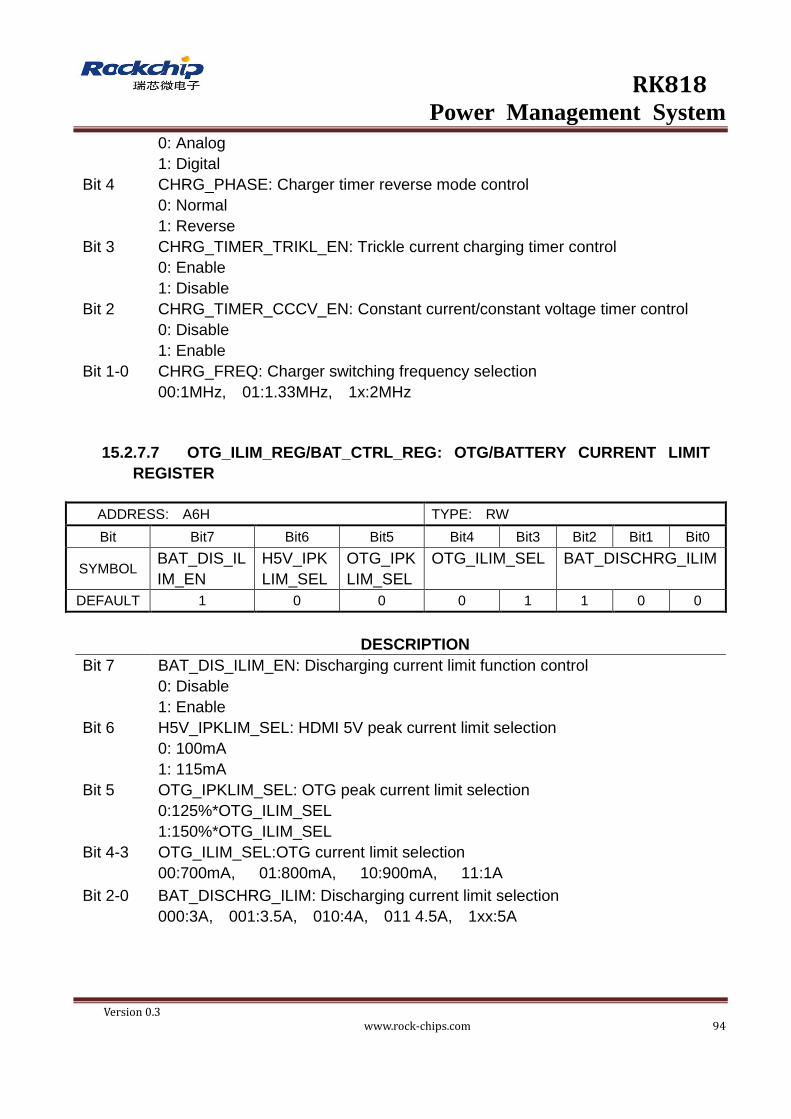
RK818 Power Management System
Version 0.3 www.rock-chips.com 94
0: Analog
1: Digital
Bit 4 CHRG_PHASE: Charger timer reverse mode control
0: Normal
1: Reverse
Bit 3 CHRG_TIMER_TRIKL_EN: Trickle current charging timer control
0: Enable
1: Disable
Bit 2 CHRG_TIMER_CCCV_EN: Constant current/constant voltage timer control
0: Disable
1: Enable
Bit 1-0 CHRG_FREQ: Charger switching frequency selection
00:1MHz, 01:1.33MHz, 1x:2MHz
OTG_ILIM_REG/BAT_CTRL_REG: OTG/BATTERY CURRENT LIMIT 15.2.7.7
REGISTER
ADDRESS: A6H TYPE: RW
Bit Bit7 Bit6 Bit5 Bit4 Bit3 Bit2 Bit1 Bit0
SYMBOL BAT_DIS_IL
IM_EN
H5V_IPK
LIM_SEL
OTG_IPK
LIM_SEL
OTG_ILIM_SEL BAT_DISCHRG_ILIM
DEFAULT 1 0 0 0 1 1 0 0
DESCRIPTION
Bit 7 BAT_DIS_ILIM_EN: Discharging current limit function control
0: Disable
1: Enable
Bit 6 H5V_IPKLIM_SEL: HDMI 5V peak current limit selection
0: 100mA
1: 115mA
Bit 5 OTG_IPKLIM_SEL: OTG peak current limit selection
0:125%*OTG_ILIM_SEL
1:150%*OTG_ILIM_SEL
Bit 4-3 OTG_ILIM_SEL:OTG current limit selection
00:700mA, 01:800mA, 10:900mA, 11:1A
Bit 2-0 BAT_DISCHRG_ILIM: Discharging current limit selection
000:3A, 001:3.5A, 010:4A, 011 4.5A, 1xx:5A
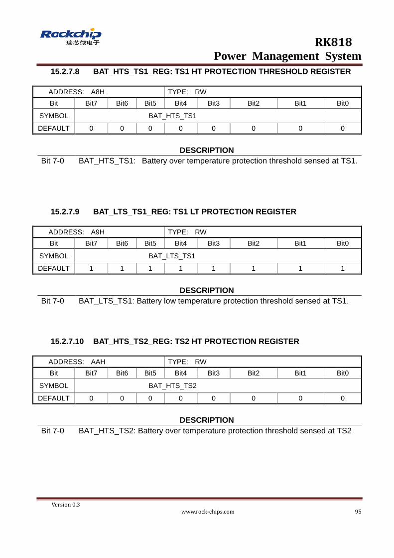
RK818 Power Management System
Version 0.3 www.rock-chips.com 95
BAT_HTS_TS1_REG: TS1 HT PROTECTION THRESHOLD REGISTER 15.2.7.8
ADDRESS: A8H TYPE: RW
Bit Bit7 Bit6 Bit5 Bit4 Bit3 Bit2 Bit1 Bit0
SYMBOL BAT_HTS_TS1
DEFAULT 0 0 0 0 0 0 0 0
DESCRIPTION
Bit 7-0 BAT_HTS_TS1: Battery over temperature protection threshold sensed at TS1.
BAT_LTS_TS1_REG: TS1 LT PROTECTION REGISTER 15.2.7.9
ADDRESS: A9H TYPE: RW
Bit Bit7 Bit6 Bit5 Bit4 Bit3 Bit2 Bit1 Bit0
SYMBOL BAT_LTS_TS1
DEFAULT 1 1 1 1 1 1 1 1
DESCRIPTION
Bit 7-0 BAT_LTS_TS1: Battery low temperature protection threshold sensed at TS1.
BAT_HTS_TS2_REG: TS2 HT PROTECTION REGISTER 15.2.7.10
ADDRESS: AAH TYPE: RW
Bit Bit7 Bit6 Bit5 Bit4 Bit3 Bit2 Bit1 Bit0
SYMBOL BAT_HTS_TS2
DEFAULT 0 0 0 0 0 0 0 0
DESCRIPTION
Bit 7-0 BAT_HTS_TS2: Battery over temperature protection threshold sensed at TS2
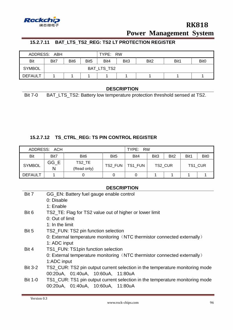
RK818 Power Management System
Version 0.3 www.rock-chips.com 96
BAT_LTS_TS2_REG: TS2 LT PROTECTION REGISTER 15.2.7.11
ADDRESS: ABH TYPE: RW
Bit Bit7 Bit6 Bit5 Bit4 Bit3 Bit2 Bit1 Bit0
SYMBOL BAT_LTS_TS2
DEFAULT 1 1 1 1 1 1 1 1
DESCRIPTION
Bit 7-0 BAT_LTS_TS2: Battery low temperature protection threshold sensed at TS2.
TS_CTRL_REG: TS PIN CONTROL REGISTER 15.2.7.12
ADDRESS: ACH TYPE: RW
Bit Bit7 Bit6 Bit5 Bit4 Bit3 Bit2 Bit1 Bit0
SYMBOL GG_E
N
TS2_TE
(Read only) TS2_FUN TS1_FUN TS2_CUR TS1_CUR
DEFAULT 1 0 0 0 1 1 1 1
DESCRIPTION
Bit 7 GG_EN: Battery fuel gauge enable control
0: Disable
1: Enable
Bit 6 TS2_TE: Flag for TS2 value out of higher or lower limit
0: Out of limit
1: In the limit
Bit 5 TS2_FUN: TS2 pin function selection
0: External temperature monitoring(NTC thermistor connected externally)
1: ADC input
Bit 4 TS1_FUN: TS1pin function selection
0: External temperature monitoring(NTC thermistor connected externally)
1:ADC input
Bit 3-2 TS2_CUR: TS2 pin output current selection in the temperature monitoring mode
00:20uA, 01:40uA, 10:60uA, 11:80uA
Bit 1-0 TS1_CUR: TS1 pin output current selection in the temperature monitoring mode
00:20uA, 01:40uA, 10:60uA, 11:80uA
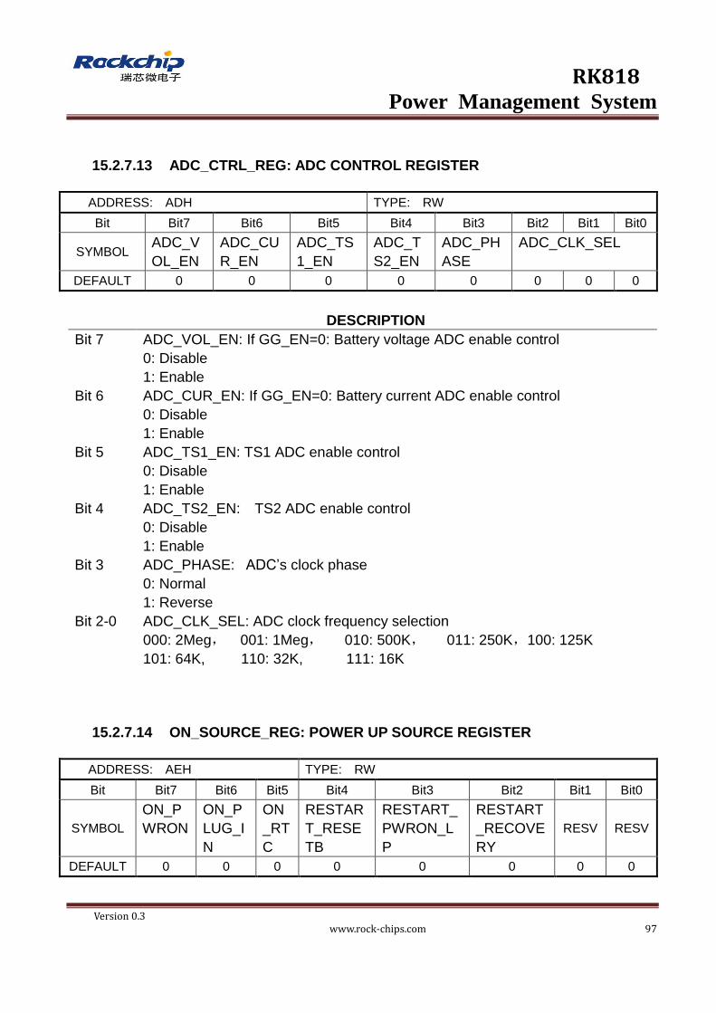
RK818 Power Management System
Version 0.3 www.rock-chips.com 97
ADC_CTRL_REG: ADC CONTROL REGISTER 15.2.7.13
ADDRESS: ADH TYPE: RW
Bit Bit7 Bit6 Bit5 Bit4 Bit3 Bit2 Bit1 Bit0
SYMBOL ADC_V
OL_EN
ADC_CU
R_EN
ADC_TS
1_EN
ADC_T
S2_EN
ADC_PH
ASE
ADC_CLK_SEL
DEFAULT 0 0 0 0 0 0 0 0
DESCRIPTION
Bit 7 ADC_VOL_EN: If GG_EN=0: Battery voltage ADC enable control
0: Disable
1: Enable
Bit 6 ADC_CUR_EN: If GG_EN=0: Battery current ADC enable control
0: Disable
1: Enable
Bit 5 ADC_TS1_EN: TS1 ADC enable control
0: Disable
1: Enable
Bit 4 ADC_TS2_EN: TS2 ADC enable control
0: Disable
1: Enable
Bit 3 ADC_PHASE: ADC’s clock phase
0: Normal
1: Reverse
Bit 2-0 ADC_CLK_SEL: ADC clock frequency selection
000: 2Meg, 001: 1Meg, 010: 500K, 011: 250K,100: 125K
101: 64K, 110: 32K, 111: 16K
ON_SOURCE_REG: POWER UP SOURCE REGISTER 15.2.7.14
ADDRESS: AEH TYPE: RW
Bit Bit7 Bit6 Bit5 Bit4 Bit3 Bit2 Bit1 Bit0
SYMBOL
ON_P
WRON
ON_P
LUG_I
N
ON
_RT
C
RESTAR
T_RESE
TB
RESTART_
PWRON_L
P
RESTART
_RECOVE
RY
RESV RESV
DEFAULT 0 0 0 0 0 0 0 0
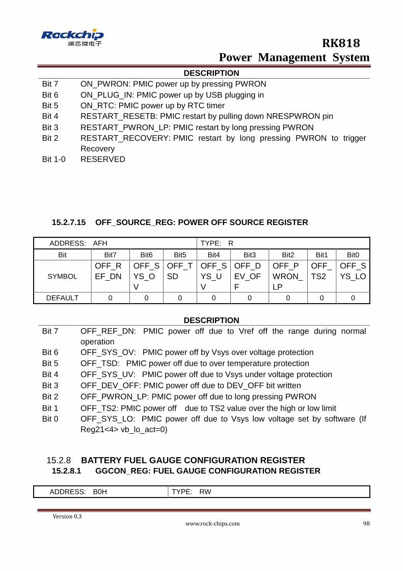
RK818 Power Management System
Version 0.3 www.rock-chips.com 98
DESCRIPTION
Bit 7 ON_PWRON: PMIC power up by pressing PWRON
Bit 6 ON_PLUG_IN: PMIC power up by USB plugging in
Bit 5 ON_RTC: PMIC power up by RTC timer
Bit 4 RESTART_RESETB: PMIC restart by pulling down NRESPWRON pin
Bit 3 RESTART_PWRON_LP: PMIC restart by long pressing PWRON
Bit 2 RESTART_RECOVERY: PMIC restart by long pressing PWRON to trigger
Recovery
Bit 1-0 RESERVED
OFF_SOURCE_REG: POWER OFF SOURCE REGISTER 15.2.7.15
ADDRESS: AFH TYPE: R
Bit Bit7 Bit6 Bit5 Bit4 Bit3 Bit2 Bit1 Bit0
SYMBOL
OFF_R
EF_DN
OFF_S
YS_O
V
OFF_T
SD
OFF_S
YS_U
V
OFF_D
EV_OF
F
OFF_P
WRON_
LP
OFF_
TS2
OFF_S
YS_LO
DEFAULT 0 0 0 0 0 0 0 0
DESCRIPTION
Bit 7 OFF_REF_DN: PMIC power off due to Vref off the range during normal
operation
Bit 6 OFF_SYS_OV: PMIC power off by Vsys over voltage protection
Bit 5 OFF_TSD: PMIC power off due to over temperature protection
Bit 4 OFF_SYS_UV: PMIC power off due to Vsys under voltage protection
Bit 3 OFF_DEV_OFF: PMIC power off due to DEV_OFF bit written
Bit 2 OFF_PWRON_LP: PMIC power off due to long pressing PWRON
Bit 1 OFF_TS2: PMIC power off due to TS2 value over the high or low limit
Bit 0 OFF_SYS_LO: PMIC power off due to Vsys low voltage set by software (If
Reg21<4> vb_lo_act=0)
BATTERY FUEL GAUGE CONFIGURATION REGISTER 15.2.8
GGCON_REG: FUEL GAUGE CONFIGURATION REGISTER 15.2.8.1
ADDRESS: B0H TYPE: RW
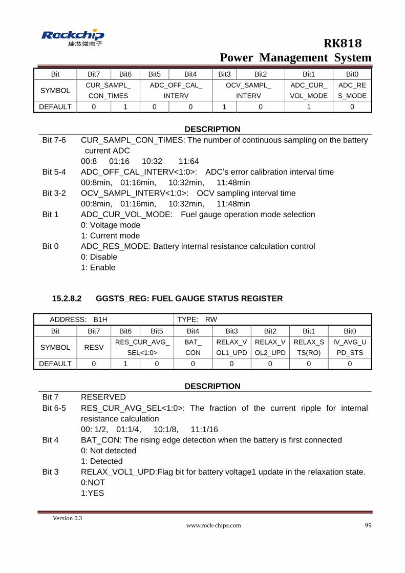
RK818 Power Management System
Version 0.3 www.rock-chips.com 99
Bit Bit7 Bit6 Bit5 Bit4 Bit3 Bit2 Bit1 Bit0
SYMBOL CUR_SAMPL_
CON_TIMES
ADC_OFF_CAL_
INTERV
OCV_SAMPL_
INTERV
ADC_CUR_
VOL_MODE
ADC_RE
S_MODE
DEFAULT 0 1 0 0 1 0 1 0
DESCRIPTION
Bit 7-6 CUR_SAMPL_CON_TIMES: The number of continuous sampling on the battery
current ADC
00:8 01:16 10:32 11:64
Bit 5-4 ADC_OFF_CAL_INTERV<1:0>: ADC’s error calibration interval time
00:8min, 01:16min, 10:32min, 11:48min
Bit 3-2 OCV_SAMPL_INTERV<1:0>: OCV sampling interval time
00:8min, 01:16min, 10:32min, 11:48min
Bit 1 ADC_CUR_VOL_MODE: Fuel gauge operation mode selection
0: Voltage mode
1: Current mode
Bit 0 ADC_RES_MODE: Battery internal resistance calculation control
0: Disable
1: Enable
GGSTS_REG: FUEL GAUGE STATUS REGISTER 15.2.8.2
ADDRESS: B1H TYPE: RW
Bit Bit7 Bit6 Bit5 Bit4 Bit3 Bit2 Bit1 Bit0
SYMBOL RESV RES_CUR_AVG_
SEL<1:0>
BAT_
CON
RELAX_V
OL1_UPD
RELAX_V
OL2_UPD
RELAX_S
TS(RO)
IV_AVG_U
PD_STS
DEFAULT 0 1 0 0 0 0 0 0
DESCRIPTION
Bit 7 RESERVED
Bit 6-5 RES_CUR_AVG_SEL<1:0>: The fraction of the current ripple for internal
resistance calculation
00: 1/2, 01:1/4, 10:1/8, 11:1/16
Bit 4 BAT_CON: The rising edge detection when the battery is first connected
0: Not detected
1: Detected
Bit 3 RELAX_VOL1_UPD:Flag bit for battery voltage1 update in the relaxation state.
0:NOT
1:YES
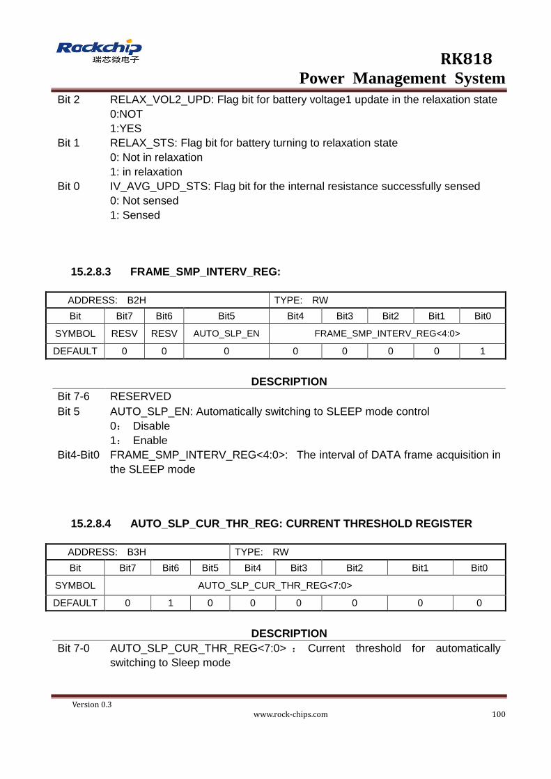
RK818 Power Management System
Version 0.3 www.rock-chips.com 100
Bit 2 RELAX_VOL2_UPD: Flag bit for battery voltage1 update in the relaxation state
0:NOT
1:YES
Bit 1 RELAX_STS: Flag bit for battery turning to relaxation state
0: Not in relaxation
1: in relaxation
Bit 0 IV_AVG_UPD_STS: Flag bit for the internal resistance successfully sensed
0: Not sensed
1: Sensed
FRAME_SMP_INTERV_REG: 15.2.8.3
ADDRESS: B2H TYPE: RW
Bit Bit7 Bit6 Bit5 Bit4 Bit3 Bit2 Bit1 Bit0
SYMBOL RESV RESV AUTO_SLP_EN FRAME_SMP_INTERV_REG<4:0>
DEFAULT 0 0 0 0 0 0 0 1
DESCRIPTION
Bit 7-6 RESERVED
Bit 5 AUTO_SLP_EN: Automatically switching to SLEEP mode control
0: Disable
1: Enable
Bit4-Bit0 FRAME_SMP_INTERV_REG<4:0>: The interval of DATA frame acquisition in
the SLEEP mode
AUTO_SLP_CUR_THR_REG: CURRENT THRESHOLD REGISTER 15.2.8.4
ADDRESS: B3H TYPE: RW
Bit Bit7 Bit6 Bit5 Bit4 Bit3 Bit2 Bit1 Bit0
SYMBOL AUTO_SLP_CUR_THR_REG<7:0>
DEFAULT 0 1 0 0 0 0 0 0
DESCRIPTION
Bit 7-0 AUTO_SLP_CUR_THR_REG<7:0> : Current threshold for automatically
switching to Sleep mode
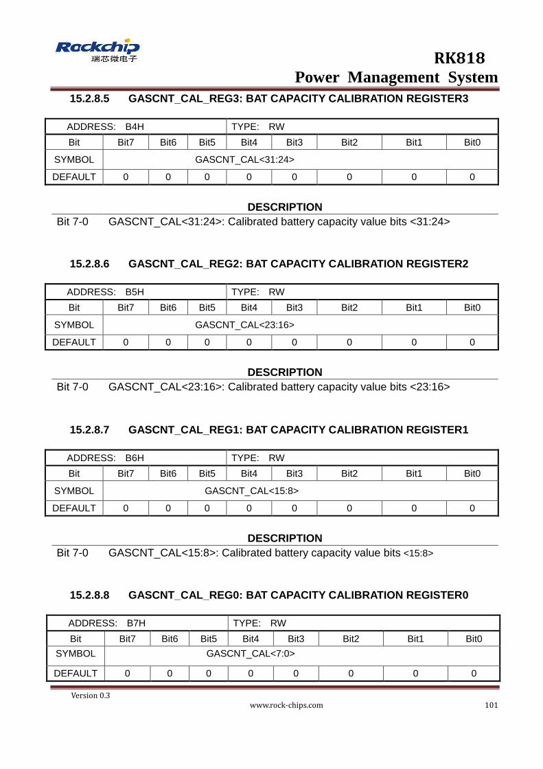
RK818 Power Management System
Version 0.3 www.rock-chips.com 101
GASCNT_CAL_REG3: BAT CAPACITY CALIBRATION REGISTER3 15.2.8.5
ADDRESS: B4H TYPE: RW
Bit Bit7 Bit6 Bit5 Bit4 Bit3 Bit2 Bit1 Bit0
SYMBOL GASCNT_CAL<31:24>
DEFAULT 0 0 0 0 0 0 0 0
DESCRIPTION
Bit 7-0 GASCNT_CAL<31:24>: Calibrated battery capacity value bits <31:24>
GASCNT_CAL_REG2: BAT CAPACITY CALIBRATION REGISTER2 15.2.8.6
ADDRESS: B5H TYPE: RW
Bit Bit7 Bit6 Bit5 Bit4 Bit3 Bit2 Bit1 Bit0
SYMBOL GASCNT_CAL<23:16>
DEFAULT 0 0 0 0 0 0 0 0
DESCRIPTION
Bit 7-0 GASCNT_CAL<23:16>: Calibrated battery capacity value bits <23:16>
GASCNT_CAL_REG1: BAT CAPACITY CALIBRATION REGISTER1 15.2.8.7
ADDRESS: B6H TYPE: RW
Bit Bit7 Bit6 Bit5 Bit4 Bit3 Bit2 Bit1 Bit0
SYMBOL GASCNT_CAL<15:8>
DEFAULT 0 0 0 0 0 0 0 0
DESCRIPTION
Bit 7-0 GASCNT_CAL<15:8>: Calibrated battery capacity value bits <15:8>
GASCNT_CAL_REG0: BAT CAPACITY CALIBRATION REGISTER0 15.2.8.8
ADDRESS: B7H TYPE: RW
Bit Bit7 Bit6 Bit5 Bit4 Bit3 Bit2 Bit1 Bit0
SYMBOL GASCNT_CAL<7:0>
DEFAULT 0 0 0 0 0 0 0 0
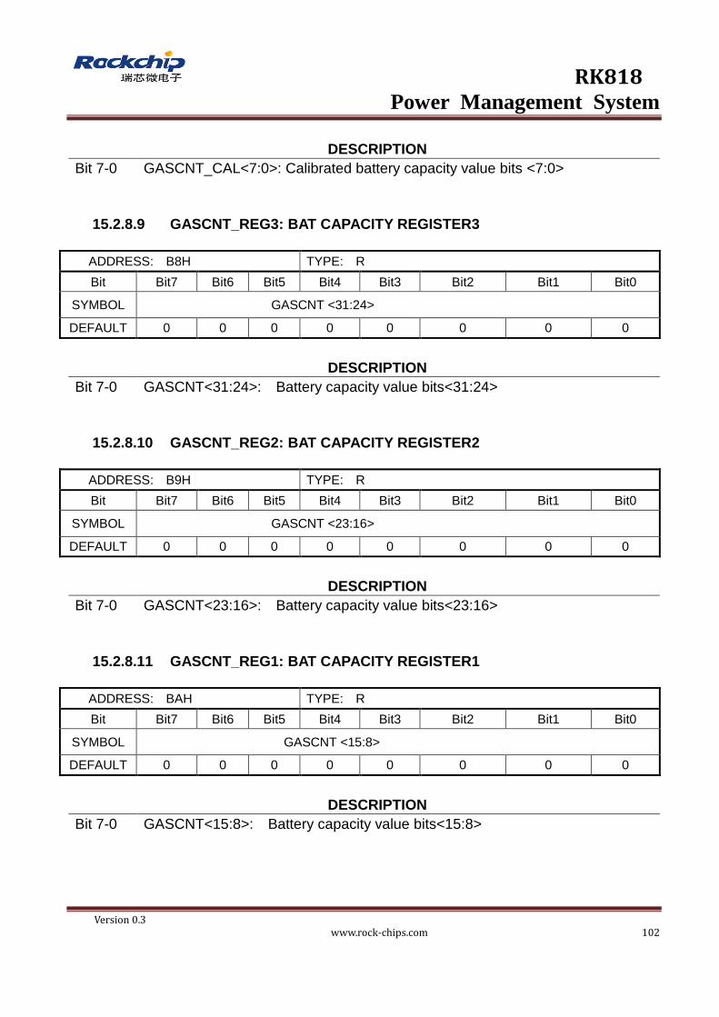
RK818 Power Management System
Version 0.3 www.rock-chips.com 102
DESCRIPTION
Bit 7-0 GASCNT_CAL<7:0>: Calibrated battery capacity value bits <7:0>
GASCNT_REG3: BAT CAPACITY REGISTER3 15.2.8.9
ADDRESS: B8H TYPE: R
Bit Bit7 Bit6 Bit5 Bit4 Bit3 Bit2 Bit1 Bit0
SYMBOL GASCNT <31:24>
DEFAULT 0 0 0 0 0 0 0 0
DESCRIPTION
Bit 7-0 GASCNT<31:24>: Battery capacity value bits<31:24>
GASCNT_REG2: BAT CAPACITY REGISTER2 15.2.8.10
ADDRESS: B9H TYPE: R
Bit Bit7 Bit6 Bit5 Bit4 Bit3 Bit2 Bit1 Bit0
SYMBOL GASCNT <23:16>
DEFAULT 0 0 0 0 0 0 0 0
DESCRIPTION
Bit 7-0 GASCNT<23:16>: Battery capacity value bits<23:16>
GASCNT_REG1: BAT CAPACITY REGISTER1 15.2.8.11
ADDRESS: BAH TYPE: R
Bit Bit7 Bit6 Bit5 Bit4 Bit3 Bit2 Bit1 Bit0
SYMBOL GASCNT <15:8>
DEFAULT 0 0 0 0 0 0 0 0
DESCRIPTION
Bit 7-0 GASCNT<15:8>: Battery capacity value bits<15:8>
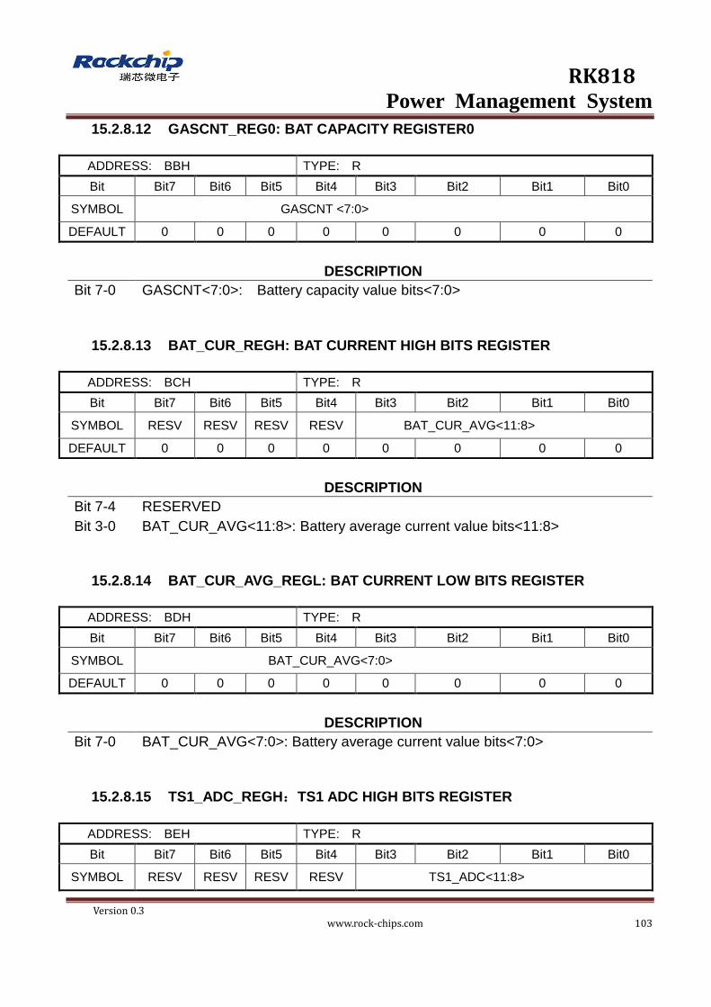
RK818 Power Management System
Version 0.3 www.rock-chips.com 103
GASCNT_REG0: BAT CAPACITY REGISTER0 15.2.8.12
ADDRESS: BBH TYPE: R
Bit Bit7 Bit6 Bit5 Bit4 Bit3 Bit2 Bit1 Bit0
SYMBOL GASCNT <7:0>
DEFAULT 0 0 0 0 0 0 0 0
DESCRIPTION
Bit 7-0 GASCNT<7:0>: Battery capacity value bits<7:0>
BAT_CUR_REGH: BAT CURRENT HIGH BITS REGISTER 15.2.8.13
ADDRESS: BCH TYPE: R
Bit Bit7 Bit6 Bit5 Bit4 Bit3 Bit2 Bit1 Bit0
SYMBOL RESV RESV RESV RESV BAT_CUR_AVG<11:8>
DEFAULT 0 0 0 0 0 0 0 0
DESCRIPTION
Bit 7-4 RESERVED
Bit 3-0 BAT_CUR_AVG<11:8>: Battery average current value bits<11:8>
BAT_CUR_AVG_REGL: BAT CURRENT LOW BITS REGISTER 15.2.8.14
ADDRESS: BDH TYPE: R
Bit Bit7 Bit6 Bit5 Bit4 Bit3 Bit2 Bit1 Bit0
SYMBOL BAT_CUR_AVG<7:0>
DEFAULT 0 0 0 0 0 0 0 0
DESCRIPTION
Bit 7-0 BAT_CUR_AVG<7:0>: Battery average current value bits<7:0>
TS1_ADC_REGH:TS1 ADC HIGH BITS REGISTER 15.2.8.15
ADDRESS: BEH TYPE: R
Bit Bit7 Bit6 Bit5 Bit4 Bit3 Bit2 Bit1 Bit0
SYMBOL RESV RESV RESV RESV TS1_ADC<11:8>
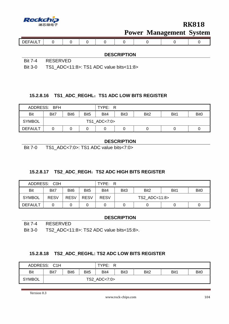
RK818 Power Management System
Version 0.3 www.rock-chips.com 104
DEFAULT 0 0 0 0 0 0 0 0
DESCRIPTION
Bit 7-4 RESERVED
Bit 3-0 TS1_ADC<11:8>: TS1 ADC value bits<11:8>
TS1_ADC_REGHL:TS1 ADC LOW BITS REGISTER 15.2.8.16
ADDRESS: BFH TYPE: R
Bit Bit7 Bit6 Bit5 Bit4 Bit3 Bit2 Bit1 Bit0
SYMBOL TS1_ADC<7:0>
DEFAULT 0 0 0 0 0 0 0 0
DESCRIPTION
Bit 7-0 TS1_ADC<7:0>: TS1 ADC value bits<7:0>
TS2_ADC_REGH:TS2 ADC HIGH BITS REGISTER 15.2.8.17
ADDRESS: C0H TYPE: R
Bit Bit7 Bit6 Bit5 Bit4 Bit3 Bit2 Bit1 Bit0
SYMBOL RESV RESV RESV RESV TS2_ADC<11:8>
DEFAULT 0 0 0 0 0 0 0 0
DESCRIPTION
Bit 7-4 RESERVED
Bit 3-0 TS2_ADC<11:8>: TS2 ADC value bits<15:8>.
TS2_ADC_REGHL: TS2 ADC LOW BITS REGISTER 15.2.8.18
ADDRESS: C1H TYPE: R
Bit Bit7 Bit6 Bit5 Bit4 Bit3 Bit2 Bit1 Bit0
SYMBOL TS2_ADC<7:0>
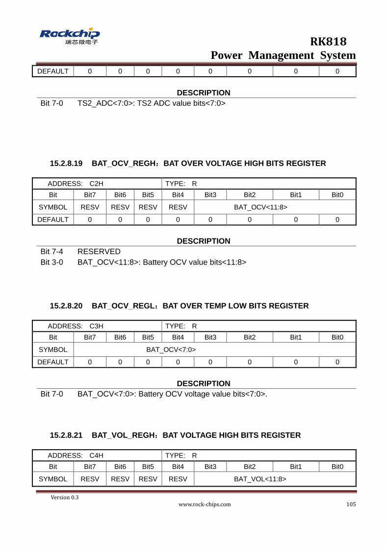
RK818 Power Management System
Version 0.3 www.rock-chips.com 105
DEFAULT 0 0 0 0 0 0 0 0
DESCRIPTION
Bit 7-0 TS2_ADC<7:0>: TS2 ADC value bits<7:0>
BAT_OCV_REGH:BAT OVER VOLTAGE HIGH BITS REGISTER 15.2.8.19
ADDRESS: C2H TYPE: R
Bit Bit7 Bit6 Bit5 Bit4 Bit3 Bit2 Bit1 Bit0
SYMBOL RESV RESV RESV RESV BAT_OCV<11:8>
DEFAULT 0 0 0 0 0 0 0 0
DESCRIPTION
Bit 7-4 RESERVED
Bit 3-0 BAT_OCV<11:8>: Battery OCV value bits<11:8>
BAT_OCV_REGL:BAT OVER TEMP LOW BITS REGISTER 15.2.8.20
ADDRESS: C3H TYPE: R
Bit Bit7 Bit6 Bit5 Bit4 Bit3 Bit2 Bit1 Bit0
SYMBOL BAT_OCV<7:0>
DEFAULT 0 0 0 0 0 0 0 0
DESCRIPTION
Bit 7-0 BAT_OCV<7:0>: Battery OCV voltage value bits<7:0>.
BAT_VOL_REGH:BAT VOLTAGE HIGH BITS REGISTER 15.2.8.21
ADDRESS: C4H TYPE: R
Bit Bit7 Bit6 Bit5 Bit4 Bit3 Bit2 Bit1 Bit0
SYMBOL RESV RESV RESV RESV BAT_VOL<11:8>
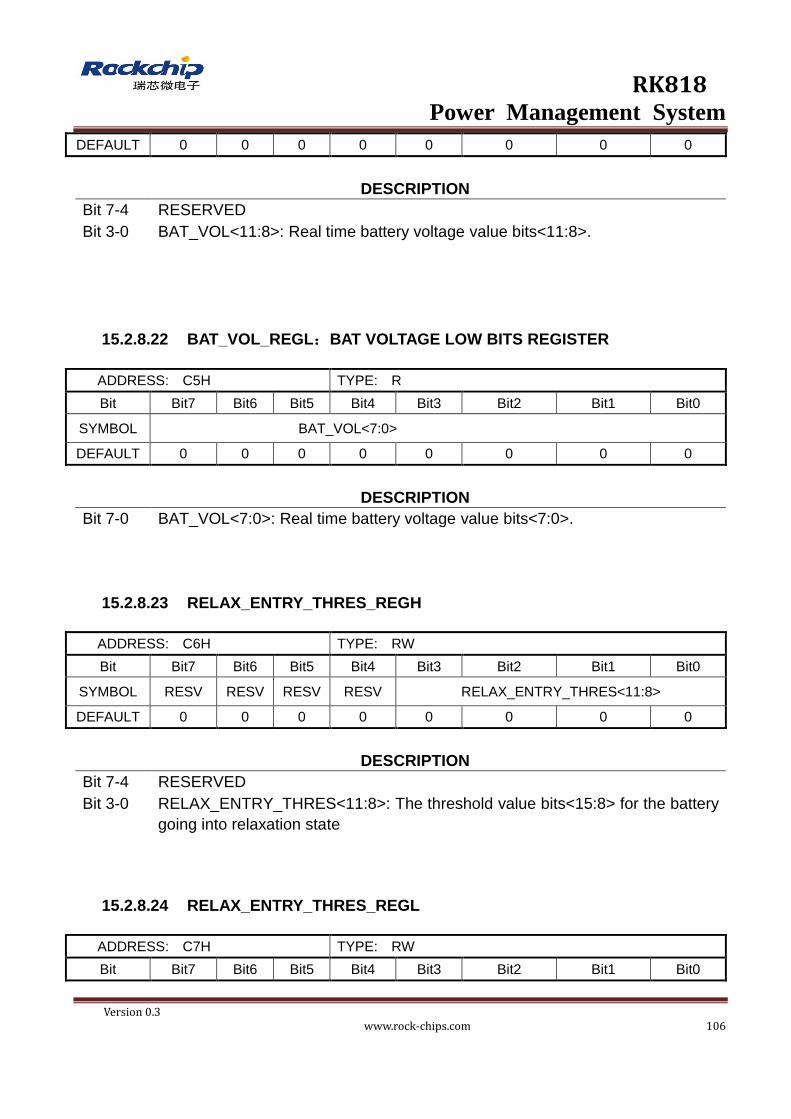
RK818 Power Management System
Version 0.3 www.rock-chips.com 106
DEFAULT 0 0 0 0 0 0 0 0
DESCRIPTION
Bit 7-4 RESERVED
Bit 3-0 BAT_VOL<11:8>: Real time battery voltage value bits<11:8>.
BAT_VOL_REGL:BAT VOLTAGE LOW BITS REGISTER 15.2.8.22
ADDRESS: C5H TYPE: R
Bit Bit7 Bit6 Bit5 Bit4 Bit3 Bit2 Bit1 Bit0
SYMBOL BAT_VOL<7:0>
DEFAULT 0 0 0 0 0 0 0 0
DESCRIPTION
Bit 7-0 BAT_VOL<7:0>: Real time battery voltage value bits<7:0>.
RELAX_ENTRY_THRES_REGH 15.2.8.23
ADDRESS: C6H TYPE: RW
Bit Bit7 Bit6 Bit5 Bit4 Bit3 Bit2 Bit1 Bit0
SYMBOL RESV RESV RESV RESV RELAX_ENTRY_THRES<11:8>
DEFAULT 0 0 0 0 0 0 0 0
DESCRIPTION
Bit 7-4 RESERVED
Bit 3-0 RELAX_ENTRY_THRES<11:8>: The threshold value bits<15:8> for the battery
going into relaxation state
RELAX_ENTRY_THRES_REGL 15.2.8.24
ADDRESS: C7H TYPE: RW
Bit Bit7 Bit6 Bit5 Bit4 Bit3 Bit2 Bit1 Bit0
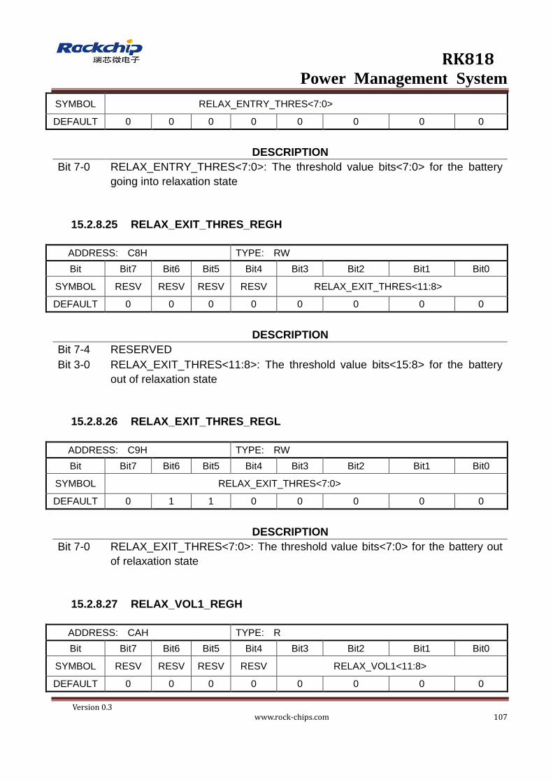
RK818 Power Management System
Version 0.3 www.rock-chips.com 107
SYMBOL RELAX_ENTRY_THRES<7:0>
DEFAULT 0 0 0 0 0 0 0 0
DESCRIPTION
Bit 7-0 RELAX_ENTRY_THRES<7:0>: The threshold value bits<7:0> for the battery
going into relaxation state
RELAX_EXIT_THRES_REGH 15.2.8.25
ADDRESS: C8H TYPE: RW
Bit Bit7 Bit6 Bit5 Bit4 Bit3 Bit2 Bit1 Bit0
SYMBOL RESV RESV RESV RESV RELAX_EXIT_THRES<11:8>
DEFAULT 0 0 0 0 0 0 0 0
DESCRIPTION
Bit 7-4 RESERVED
Bit 3-0 RELAX_EXIT_THRES<11:8>: The threshold value bits<15:8> for the battery
out of relaxation state
RELAX_EXIT_THRES_REGL 15.2.8.26
ADDRESS: C9H TYPE: RW
Bit Bit7 Bit6 Bit5 Bit4 Bit3 Bit2 Bit1 Bit0
SYMBOL RELAX_EXIT_THRES<7:0>
DEFAULT 0 1 1 0 0 0 0 0
DESCRIPTION
Bit 7-0 RELAX_EXIT_THRES<7:0>: The threshold value bits<7:0> for the battery out
of relaxation state
RELAX_VOL1_REGH 15.2.8.27
ADDRESS: CAH TYPE: R
Bit Bit7 Bit6 Bit5 Bit4 Bit3 Bit2 Bit1 Bit0
SYMBOL RESV RESV RESV RESV RELAX_VOL1<11:8>
DEFAULT 0 0 0 0 0 0 0 0
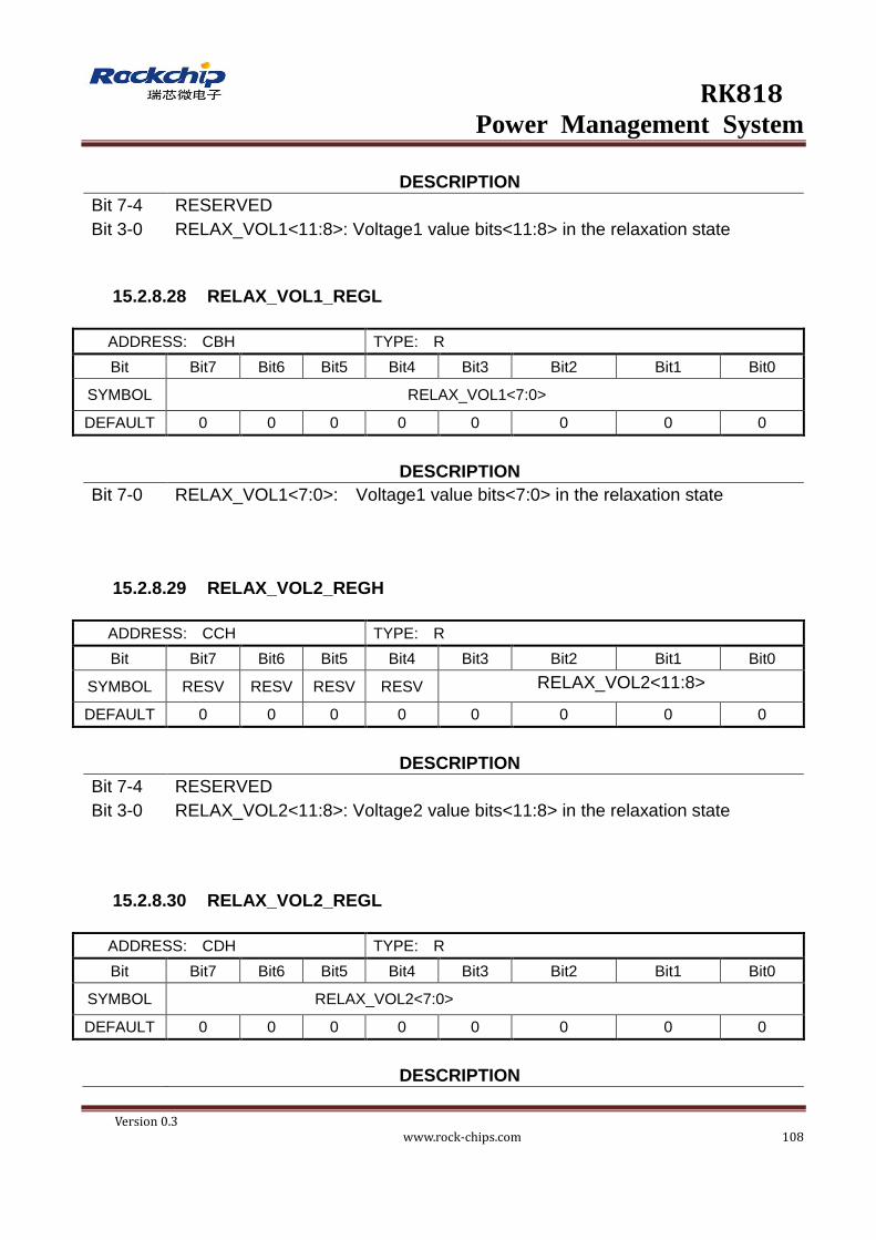
RK818 Power Management System
Version 0.3 www.rock-chips.com 108
DESCRIPTION
Bit 7-4 RESERVED
Bit 3-0 RELAX_VOL1<11:8>: Voltage1 value bits<11:8> in the relaxation state
RELAX_VOL1_REGL 15.2.8.28
ADDRESS: CBH TYPE: R
Bit Bit7 Bit6 Bit5 Bit4 Bit3 Bit2 Bit1 Bit0
SYMBOL RELAX_VOL1<7:0>
DEFAULT 0 0 0 0 0 0 0 0
DESCRIPTION
Bit 7-0 RELAX_VOL1<7:0>: Voltage1 value bits<7:0> in the relaxation state
RELAX_VOL2_REGH 15.2.8.29
ADDRESS: CCH TYPE: R
Bit Bit7 Bit6 Bit5 Bit4 Bit3 Bit2 Bit1 Bit0
SYMBOL RESV RESV RESV RESV RELAX_VOL2<11:8>
DEFAULT 0 0 0 0 0 0 0 0
DESCRIPTION
Bit 7-4 RESERVED
Bit 3-0 RELAX_VOL2<11:8>: Voltage2 value bits<11:8> in the relaxation state
RELAX_VOL2_REGL 15.2.8.30
ADDRESS: CDH TYPE: R
Bit Bit7 Bit6 Bit5 Bit4 Bit3 Bit2 Bit1 Bit0
SYMBOL RELAX_VOL2<7:0>
DEFAULT 0 0 0 0 0 0 0 0
DESCRIPTION
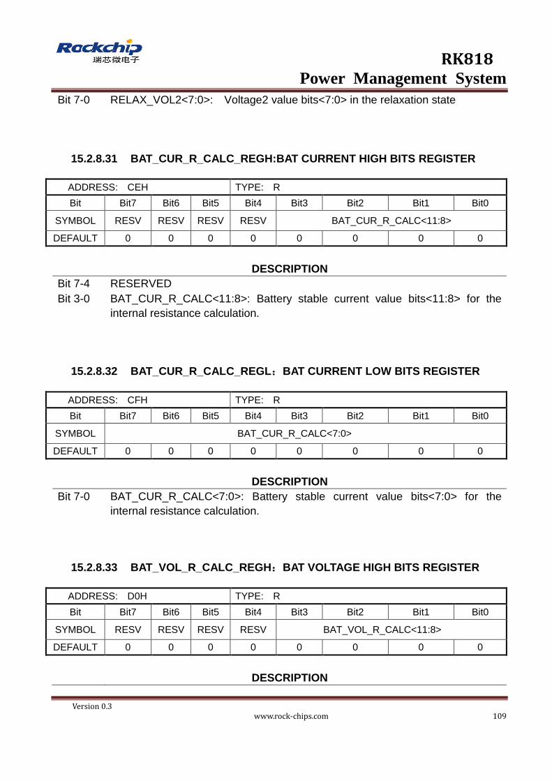
RK818 Power Management System
Version 0.3 www.rock-chips.com 109
Bit 7-0 RELAX_VOL2<7:0>: Voltage2 value bits<7:0> in the relaxation state
BAT_CUR_R_CALC_REGH:BAT CURRENT HIGH BITS REGISTER 15.2.8.31
ADDRESS: CEH TYPE: R
Bit Bit7 Bit6 Bit5 Bit4 Bit3 Bit2 Bit1 Bit0
SYMBOL RESV RESV RESV RESV BAT_CUR_R_CALC<11:8>
DEFAULT 0 0 0 0 0 0 0 0
DESCRIPTION
Bit 7-4 RESERVED
Bit 3-0 BAT_CUR_R_CALC<11:8>: Battery stable current value bits<11:8> for the
internal resistance calculation.
BAT_CUR_R_CALC_REGL:BAT CURRENT LOW BITS REGISTER 15.2.8.32
ADDRESS: CFH TYPE: R
Bit Bit7 Bit6 Bit5 Bit4 Bit3 Bit2 Bit1 Bit0
SYMBOL BAT_CUR_R_CALC<7:0>
DEFAULT 0 0 0 0 0 0 0 0
DESCRIPTION
Bit 7-0 BAT_CUR_R_CALC<7:0>: Battery stable current value bits<7:0> for the
internal resistance calculation.
BAT_VOL_R_CALC_REGH:BAT VOLTAGE HIGH BITS REGISTER 15.2.8.33
ADDRESS: D0H TYPE: R
Bit Bit7 Bit6 Bit5 Bit4 Bit3 Bit2 Bit1 Bit0
SYMBOL RESV RESV RESV RESV BAT_VOL_R_CALC<11:8>
DEFAULT 0 0 0 0 0 0 0 0
DESCRIPTION
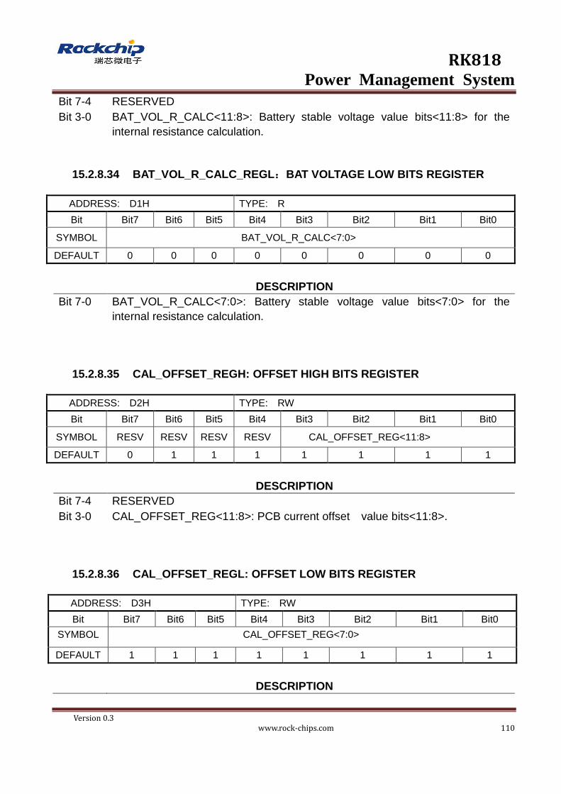
RK818 Power Management System
Version 0.3 www.rock-chips.com 110
Bit 7-4 RESERVED
Bit 3-0 BAT_VOL_R_CALC<11:8>: Battery stable voltage value bits<11:8> for the
internal resistance calculation.
BAT_VOL_R_CALC_REGL:BAT VOLTAGE LOW BITS REGISTER 15.2.8.34
ADDRESS: D1H TYPE: R
Bit Bit7 Bit6 Bit5 Bit4 Bit3 Bit2 Bit1 Bit0
SYMBOL BAT_VOL_R_CALC<7:0>
DEFAULT 0 0 0 0 0 0 0 0
DESCRIPTION
Bit 7-0 BAT_VOL_R_CALC<7:0>: Battery stable voltage value bits<7:0> for the
internal resistance calculation.
CAL_OFFSET_REGH: OFFSET HIGH BITS REGISTER 15.2.8.35
ADDRESS: D2H TYPE: RW
Bit Bit7 Bit6 Bit5 Bit4 Bit3 Bit2 Bit1 Bit0
SYMBOL RESV RESV RESV RESV CAL_OFFSET_REG<11:8>
DEFAULT 0 1 1 1 1 1 1 1
DESCRIPTION
Bit 7-4 RESERVED
Bit 3-0 CAL_OFFSET_REG<11:8>: PCB current offset value bits<11:8>.
CAL_OFFSET_REGL: OFFSET LOW BITS REGISTER 15.2.8.36
ADDRESS: D3H TYPE: RW
Bit Bit7 Bit6 Bit5 Bit4 Bit3 Bit2 Bit1 Bit0
SYMBOL CAL_OFFSET_REG<7:0>
DEFAULT 1 1 1 1 1 1 1 1
DESCRIPTION
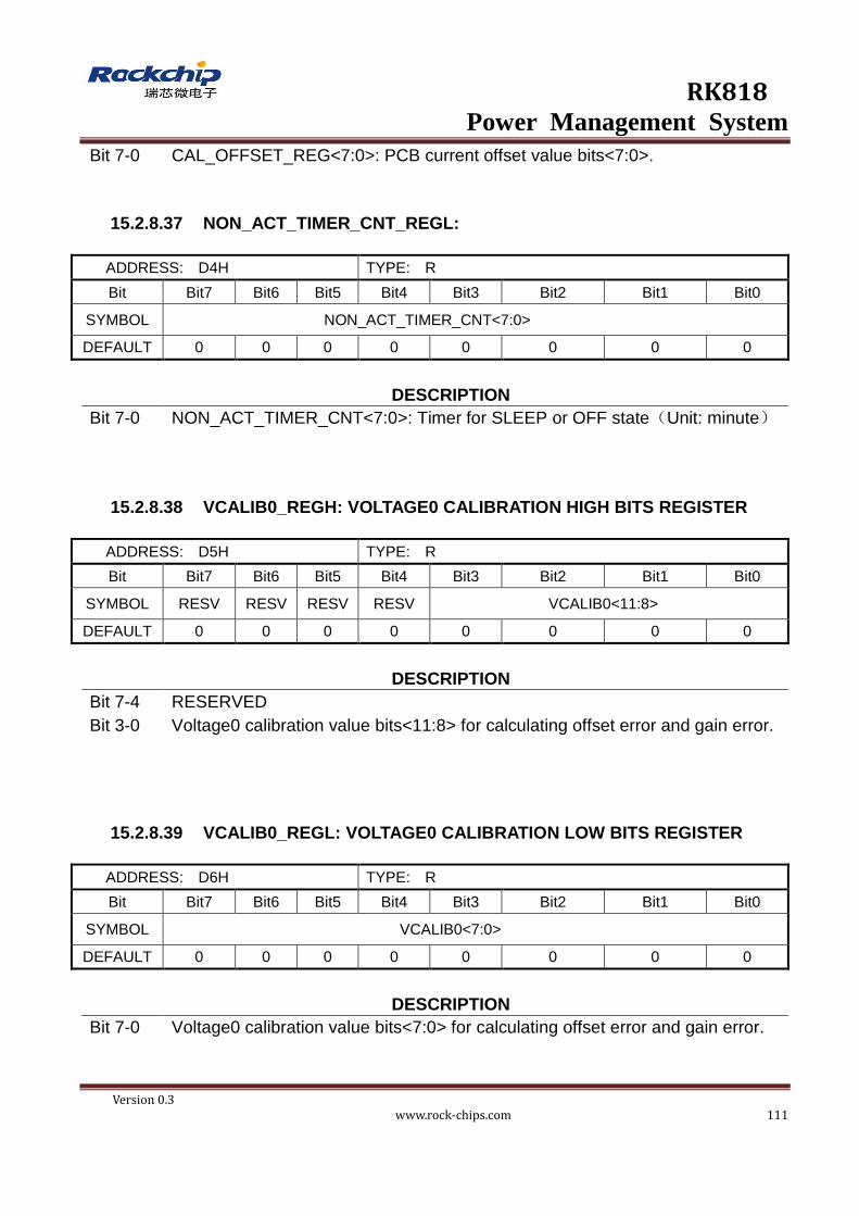
RK818 Power Management System
Version 0.3 www.rock-chips.com 111
Bit 7-0 CAL_OFFSET_REG<7:0>: PCB current offset value bits<7:0>.
NON_ACT_TIMER_CNT_REGL: 15.2.8.37
ADDRESS: D4H TYPE: R
Bit Bit7 Bit6 Bit5 Bit4 Bit3 Bit2 Bit1 Bit0
SYMBOL NON_ACT_TIMER_CNT<7:0>
DEFAULT 0 0 0 0 0 0 0 0
DESCRIPTION
Bit 7-0 NON_ACT_TIMER_CNT<7:0>: Timer for SLEEP or OFF state(Unit: minute)
VCALIB0_REGH: VOLTAGE0 CALIBRATION HIGH BITS REGISTER 15.2.8.38
ADDRESS: D5H TYPE: R
Bit Bit7 Bit6 Bit5 Bit4 Bit3 Bit2 Bit1 Bit0
SYMBOL RESV RESV RESV RESV VCALIB0<11:8>
DEFAULT 0 0 0 0 0 0 0 0
DESCRIPTION
Bit 7-4 RESERVED
Bit 3-0 Voltage0 calibration value bits<11:8> for calculating offset error and gain error.
VCALIB0_REGL: VOLTAGE0 CALIBRATION LOW BITS REGISTER 15.2.8.39
ADDRESS: D6H TYPE: R
Bit Bit7 Bit6 Bit5 Bit4 Bit3 Bit2 Bit1 Bit0
SYMBOL VCALIB0<7:0>
DEFAULT 0 0 0 0 0 0 0 0
DESCRIPTION
Bit 7-0 Voltage0 calibration value bits<7:0> for calculating offset error and gain error.
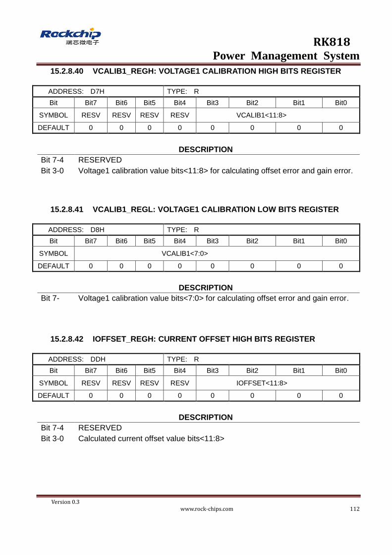
RK818 Power Management System
Version 0.3 www.rock-chips.com 112
VCALIB1_REGH: VOLTAGE1 CALIBRATION HIGH BITS REGISTER 15.2.8.40
ADDRESS: D7H TYPE: R
Bit Bit7 Bit6 Bit5 Bit4 Bit3 Bit2 Bit1 Bit0
SYMBOL RESV RESV RESV RESV VCALIB1<11:8>
DEFAULT 0 0 0 0 0 0 0 0
DESCRIPTION
Bit 7-4 RESERVED
Bit 3-0 Voltage1 calibration value bits<11:8> for calculating offset error and gain error.
VCALIB1_REGL: VOLTAGE1 CALIBRATION LOW BITS REGISTER 15.2.8.41
ADDRESS: D8H TYPE: R
Bit Bit7 Bit6 Bit5 Bit4 Bit3 Bit2 Bit1 Bit0
SYMBOL VCALIB1<7:0>
DEFAULT 0 0 0 0 0 0 0 0
DESCRIPTION
Bit 7- Voltage1 calibration value bits<7:0> for calculating offset error and gain error.
IOFFSET_REGH: CURRENT OFFSET HIGH BITS REGISTER 15.2.8.42
ADDRESS: DDH TYPE: R
Bit Bit7 Bit6 Bit5 Bit4 Bit3 Bit2 Bit1 Bit0
SYMBOL RESV RESV RESV RESV IOFFSET<11:8>
DEFAULT 0 0 0 0 0 0 0 0
DESCRIPTION
Bit 7-4 RESERVED
Bit 3-0 Calculated current offset value bits<11:8>
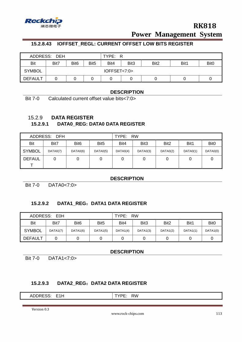
RK818 Power Management System
Version 0.3 www.rock-chips.com 113
IOFFSET_REGL: CURRENT OFFSET LOW BITS REGISTER 15.2.8.43
ADDRESS: DEH TYPE: R
Bit Bit7 Bit6 Bit5 Bit4 Bit3 Bit2 Bit1 Bit0
SYMBOL IOFFSET<7:0>
DEFAULT 0 0 0 0 0 0 0 0
DESCRIPTION
Bit 7-0 Calculated current offset value bits<7:0>
DATA REGISTER 15.2.9
DATA0_REG: DATA0 DATA REGISTER 15.2.9.1
ADDRESS: DFH TYPE: RW
Bit Bit7 Bit6 Bit5 Bit4 Bit3 Bit2 Bit1 Bit0
SYMBOL DATA0(7) DATA0(6) DATA0(5) DATA0(4) DATA0(3) DATA0(2) DATA0(1) DATA0(0)
DEFAUL
T
0 0 0 0 0 0 0 0
DESCRIPTION
Bit 7-0 DATA0<7:0>
DATA1_REG:DATA1 DATA REGISTER 15.2.9.2
ADDRESS: E0H TYPE: RW
Bit Bit7 Bit6 Bit5 Bit4 Bit3 Bit2 Bit1 Bit0
SYMBOL DATA1(7) DATA1(6) DATA1(5) DATA1(4) DATA1(3) DATA1(2) DATA1(1) DATA1(0)
DEFAULT 0 0 0 0 0 0 0 0
DESCRIPTION
Bit 7-0 DATA1<7:0>
DATA2_REG:DATA2 DATA REGISTER 15.2.9.3
ADDRESS: E1H TYPE: RW
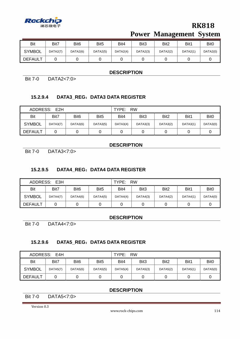
RK818 Power Management System
Version 0.3 www.rock-chips.com 114
Bit Bit7 Bit6 Bit5 Bit4 Bit3 Bit2 Bit1 Bit0
SYMBOL DATA2(7) DATA2(6) DATA2(5) DATA2(4) DATA2(3) DATA2(2) DATA2(1) DATA2(0)
DEFAULT 0 0 0 0 0 0 0 0
DESCRIPTION
Bit 7-0 DATA2<7:0>
DATA3_REG:DATA3 DATA REGISTER 15.2.9.4
ADDRESS: E2H TYPE: RW
Bit Bit7 Bit6 Bit5 Bit4 Bit3 Bit2 Bit1 Bit0
SYMBOL DATA3(7) DATA3(6) DATA3(5) DATA3(4) DATA3(3) DATA3(2) DATA3(1) DATA3(0)
DEFAULT 0 0 0 0 0 0 0 0
DESCRIPTION
Bit 7-0 DATA3<7:0>
DATA4_REG:DATA4 DATA REGISTER 15.2.9.5
ADDRESS: E3H TYPE: RW
Bit Bit7 Bit6 Bit5 Bit4 Bit3 Bit2 Bit1 Bit0
SYMBOL DATA4(7) DATA4(6) DATA4(5) DATA4(4) DATA4(3) DATA4(2) DATA4(1) DATA4(0)
DEFAULT 0 0 0 0 0 0 0 0
DESCRIPTION
Bit 7-0 DATA4<7:0>
DATA5_REG:DATA5 DATA REGISTER 15.2.9.6
ADDRESS: E4H TYPE: RW
Bit Bit7 Bit6 Bit5 Bit4 Bit3 Bit2 Bit1 Bit0
SYMBOL DATA5(7) DATA5(6) DATA5(5) DATA5(4) DATA5(3) DATA5(2) DATA5(1) DATA5(0)
DEFAULT 0 0 0 0 0 0 0 0
DESCRIPTION
Bit 7-0 DATA5<7:0>
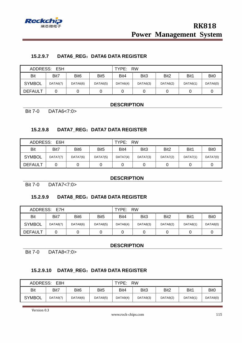
RK818 Power Management System
Version 0.3 www.rock-chips.com 115
DATA6_REG:DATA6 DATA REGISTER 15.2.9.7
ADDRESS: E5H TYPE: RW
Bit Bit7 Bit6 Bit5 Bit4 Bit3 Bit2 Bit1 Bit0
SYMBOL DATA6(7) DATA6(6) DATA6(5) DATA6(4) DATA6(3) DATA6(2) DATA6(1) DATA6(0)
DEFAULT 0 0 0 0 0 0 0 0
DESCRIPTION
Bit 7-0 DATA6<7:0>
DATA7_REG:DATA7 DATA REGISTER 15.2.9.8
ADDRESS: E6H TYPE: RW
Bit Bit7 Bit6 Bit5 Bit4 Bit3 Bit2 Bit1 Bit0
SYMBOL DATA7(7) DATA7(6) DATA7(5) DATA7(4) DATA7(3) DATA7(2) DATA7(1) DATA7(0)
DEFAULT 0 0 0 0 0 0 0 0
DESCRIPTION
Bit 7-0 DATA7<7:0>
DATA8_REG:DATA8 DATA REGISTER 15.2.9.9
ADDRESS: E7H TYPE: RW
Bit Bit7 Bit6 Bit5 Bit4 Bit3 Bit2 Bit1 Bit0
SYMBOL DATA8(7) DATA8(6) DATA8(5) DATA8(4) DATA8(3) DATA8(2) DATA8(1) DATA8(0)
DEFAULT 0 0 0 0 0 0 0 0
DESCRIPTION
Bit 7-0 DATA8<7:0>
DATA9_REG:DATA9 DATA REGISTER 15.2.9.10
ADDRESS: E8H TYPE: RW
Bit Bit7 Bit6 Bit5 Bit4 Bit3 Bit2 Bit1 Bit0
SYMBOL DATA9(7) DATA9(6) DATA9(5) DATA9(4) DATA9(3) DATA9(2) DATA9(1) DATA9(0)
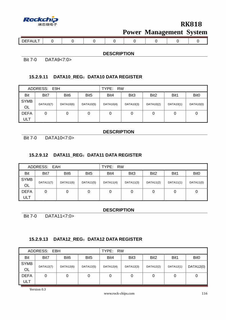
RK818 Power Management System
Version 0.3 www.rock-chips.com 116
DEFAULT 0 0 0 0 0 0 0 0
DESCRIPTION
Bit 7-0 DATA9<7:0>
DATA10_REG:DATA10 DATA REGISTER 15.2.9.11
ADDRESS: E9H TYPE: RW
Bit Bit7 Bit6 Bit5 Bit4 Bit3 Bit2 Bit1 Bit0
SYMB
OL DATA10(7) DATA10(6) DATA10(5) DATA10(4) DATA10(3) DATA10(2) DATA10(1) DATA10(0)
DEFA
ULT
0 0 0 0 0 0 0 0
DESCRIPTION
Bit 7-0 DATA10<7:0>
DATA11_REG:DATA11 DATA REGISTER 15.2.9.12
ADDRESS: EAH TYPE: RW
Bit Bit7 Bit6 Bit5 Bit4 Bit3 Bit2 Bit1 Bit0
SYMB
OL DATA11(7) DATA11(6) DATA11(5) DATA11(4) DATA11(3) DATA11(2) DATA11(1) DATA11(0)
DEFA
ULT
0 0 0 0 0 0 0 0
DESCRIPTION
Bit 7-0 DATA11<7:0>
DATA12_REG:DATA12 DATA REGISTER 15.2.9.13
ADDRESS: EBH TYPE: RW
Bit Bit7 Bit6 Bit5 Bit4 Bit3 Bit2 Bit1 Bit0
SYMB
OL DATA12(7) DATA12(6) DATA12(5) DATA12(4) DATA12(3) DATA12(2) DATA12(1) DATA12(0)
DEFA
ULT
0 0 0 0 0 0 0 0
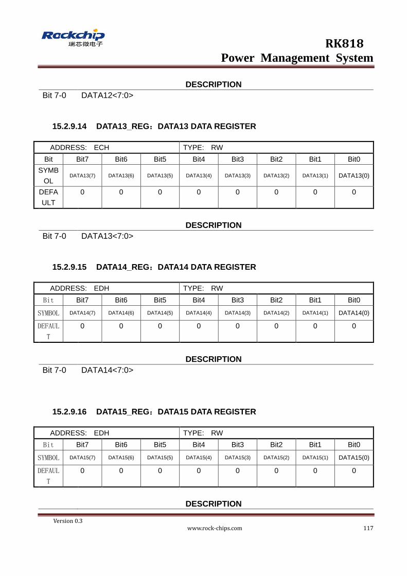
RK818 Power Management System
Version 0.3 www.rock-chips.com 117
DESCRIPTION
Bit 7-0 DATA12<7:0>
DATA13_REG:DATA13 DATA REGISTER 15.2.9.14
ADDRESS: ECH TYPE: RW
Bit Bit7 Bit6 Bit5 Bit4 Bit3 Bit2 Bit1 Bit0
SYMB
OL DATA13(7) DATA13(6) DATA13(5) DATA13(4) DATA13(3) DATA13(2) DATA13(1) DATA13(0)
DEFA
ULT
0 0 0 0 0 0 0 0
DESCRIPTION
Bit 7-0 DATA13<7:0>
DATA14_REG:DATA14 DATA REGISTER 15.2.9.15
ADDRESS: EDH TYPE: RW
Bit Bit7 Bit6 Bit5 Bit4 Bit3 Bit2 Bit1 Bit0
SYMBOL DATA14(7) DATA14(6) DATA14(5) DATA14(4) DATA14(3) DATA14(2) DATA14(1) DATA14(0)
DEFAUL
T
0 0 0 0 0 0 0 0
DESCRIPTION
Bit 7-0 DATA14<7:0>
DATA15_REG:DATA15 DATA REGISTER 15.2.9.16
ADDRESS: EDH TYPE: RW
Bit Bit7 Bit6 Bit5 Bit4 Bit3 Bit2 Bit1 Bit0
SYMBOL DATA15(7) DATA15(6) DATA15(5) DATA15(4) DATA15(3) DATA15(2) DATA15(1) DATA15(0)
DEFAUL
T
0 0 0 0 0 0 0 0
DESCRIPTION
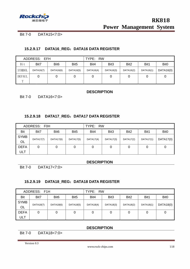
RK818 Power Management System
Version 0.3 www.rock-chips.com 118
Bit 7-0 DATA15<7:0>
DATA16_REG:DATA16 DATA REGISTER 15.2.9.17
ADDRESS: EFH TYPE: RW
Bit Bit7 Bit6 Bit5 Bit4 Bit3 Bit2 Bit1 Bit0
SYMBOL DATA16(7) DATA16(6) DATA16(5) DATA16(4) DATA16(3) DATA16(2) DATA16(1) DATA16(0)
DEFAUL
T
0 0 0 0 0 0 0 0
DESCRIPTION
Bit 7-0 DATA16<7:0>
DATA17_REG:DATA17 DATA REGISTER 15.2.9.18
ADDRESS: F0H TYPE: RW
Bit Bit7 Bit6 Bit5 Bit4 Bit3 Bit2 Bit1 Bit0
SYMB
OL DATA17(7) DATA17(6) DATA17(5) DATA17(4) DATA17(3) DATA17(2) DATA17(1) DATA17(0)
DEFA
ULT
0 0 0 0 0 0 0 0
DESCRIPTION
Bit 7-0 DATA17<7:0>
DATA18_REG:DATA18 DATA REGISTER 15.2.9.19
ADDRESS: F1H TYPE: RW
Bit Bit7 Bit6 Bit5 Bit4 Bit3 Bit2 Bit1 Bit0
SYMB
OL DATA18(7) DATA18(6) DATA18(5) DATA18(4) DATA18(3) DATA18(2) DATA18(1) DATA18(0)
DEFA
ULT
0 0 0 0 0 0 0 0
DESCRIPTION
Bit 7-0 DATA18<7:0>
RK818 Power Management System
Version 0.3 www.rock-chips.com 119
DATA19_REG:DATA19 DATA REGISTER 15.2.9.20
ADDRESS: F2H TYPE: RW
Bit Bit7 Bit6 Bit5 Bit4 Bit3 Bit2 Bit1 Bit0
SYMB
OL DATA19(7) DATA19(6) DATA19(5) DATA19(4) DATA19(3) DATA19(2) DATA19(1) DATA19(0)
DEFA
ULT
0 0 0 0 0 0 0 0
DESCRIPTION
Bit 7-0 DATA19<7:0>
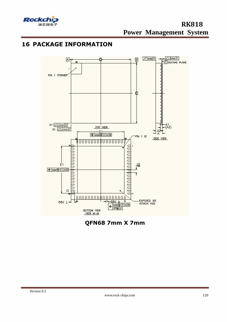
RK818 Power Management System
Version 0.3 www.rock-chips.com 120
16 PACKAGE INFORMATION
QFN68 7mm X 7mm
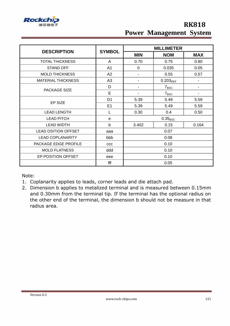
RK818 Power Management System
Version 0.3 www.rock-chips.com 121
DESCRIPTION SYMBOL MILLIMETER
MIN NOM MAX
TOTAL THICKNESS A 0.70 0.75 0.80
STAND OFF A1 0 0.035 0.05
MOLD THICKNESS A2 - 0.55 0.57
MATERIAL THICKNESS A3 - 0.203REF -
PACKAGE SIZE D - 7BSC -
E - 7BSC -
EP SIZE D1 5.39 5.49 5.59
E1 5.39 5.49 5.59
LEAD LENGTH L 0.30 0.4 0.50
LEAD PITCH e 0.35BSC
LEAD WIDTH b 3.402 0.15 0.164
LEAD OSITION OFFSET aaa 0.07
LEAD COPLANARITY bbb 0.08
PACKAGE EDGE PROFILE ccc 0.10
MOLD FLATNESS ddd 0.10
EP POSITION OFFSET eee 0.10
fff 0.05
Note:
1. Coplanarity applies to leads, corner leads and die attach pad.
2. Dimension b applies to metalized terminal and is measured between 0.15mm
and 0.30mm from the terminal tip. If the terminal has the optional radius on
the other end of the terminal, the dimension b should not be measure in that
radius area.