Embed Size (px)
Citation preview

LNK302/304-306LinkSwitch-TN FamilyLowest Component Count, Energy Efficient Off-Line Switcher IC
Figure 1. Typical Buck Converter Application (See Application Examples Section for Other Circuit Configurations).
Product HighlightsCost Effective Linear/Cap Dropper Replacement• Lowest cost and component count buck converter solution• Fully integrated auto-restart for short-circuit and open
loop fault protection – saves external component costs• LNK302 uses a simplified controller without auto-restart
for very low system cost• 66 kHz operation with accurate current limit – allows low cost
off-the-shelf 1 mH inductor for up to 120 mA output current• Tight tolerances and negligible temperature variation• High breakdown voltage of 700 V provides excellent
input surge withstand• Frequency jittering dramatically reduces EMI (~10 dB) – minimizes EMI filter cost• High thermal shutdown temperature (+135 °C minimum)
Much Higher Performance over Discrete Buck and Passive Solutions• Supports buck, buck-boost and flyback topologies• System level thermal overload, output short-circuit and
open control loop protection• Excellent line and load regulation even with typical
configuration• High bandwidth provides fast turn-on with no overshoot• Current limit operation rejects line ripple• Universal input voltage range (85 VAC to 265 VAC)• Built-in current limit and hysteretic thermal protection• Higher efficiency than passive solutions• Higher power factor than capacitor-fed solutions• Entirely manufacturable in SMD EcoSmartÈ– Extremely Energy Efficient• Consumes typically only 50/80 mW in self-powered buck
topology at 115/230 VAC input with no load (opto feedback)• Consumes typically only 7/12 mW in flyback topology
with external bias at 115/230 VAC input with no load• Meets California Energy Commission (CEC), Energy
Star, and EU requirements
Applications• Appliances and timers• LED drivers and industrial controls
DescriptionLinkSwitch-TN is specifically designed to replace all linear and capacitor-fed (cap dropper) non-isolated power supplies in the
È
Table 1. Notes: 1. Typical output current in a non-isolated buck converter. Output power capability depends on respective output voltage. See Key Applications Considerations Section for complete description of assumptions, including fully discontinuous conduction mode (DCM) operation. 2. Mostly discontinuous conduction mode. 3. Continuous conduction mode. 4. Packages: P: DIP-8B, G: SMD-8B. For lead-free package options, see Part Ordering Information.
under 360 mA output current range at equal system cost while offering much higher performance and energy efficiency.
LinkSwitch-TN devices integrate a 700 V power MOSFET, oscillator, simple On/Off control scheme, a high voltage switched current source, frequency jittering, cycle-by-cycle current limit and thermal shutdown circuitry onto a monolithic IC. The start-up and operating power are derived directly from the voltage on the DRAIN pin, eliminating the need for a bias supply and associated circuitry in buck or flyback converters. The fully integrated auto-restart circuit in the LNK304-306 safely limits output power during fault conditions such as short-circuit or open loop, reducing component count and system-level load protection cost. A local supply provided by the IC allows use of a non-safety graded optocoupler acting as a level shifter to further enhance line and load regulation performance in buck and buck-boost converters, if required.
March 2005
OUTPUT CURRENT TABLE1
PRODUCT4230 VAC ±15% 85-265 VAC
MDCM2 CCM3 MDCM2 CCM3
LNK302P or G 63 mA 80 mA 63 mA 80 mALNK304P or G 120 mA 170 mA 120 mA 170 mALNK305P or G 175 mA 280 mA 175 mA 280 mALNK306P or G 225 mA 360 mA 225 mA 360 mA
DC Output
Wide RangeHV DC Input
PI-3492-111903
+ +
FB BP
SD
LinkSwitch-TN
2
LNK302/304-306
G3/05
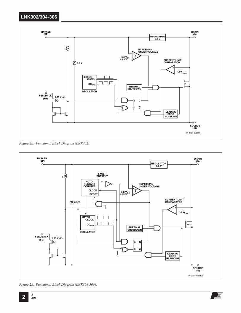
Figure 2a. Functional Block Diagram (LNK302).
PI-2367-021105
CLOCKJITTER
OSCILLATOR
5.8 V4.85 V
SOURCE(S)
S
R
Q
DCMAX
BYPASS(BP)
FAULTPRESENT
+
- VILIMIT
LEADINGEDGE
BLANKING
THERMALSHUTDOWN
+
-
DRAIN(D)
REGULATOR5.8 V
BYPASS PINUNDER-VOLTAGE
CURRENT LIMITCOMPARATOR
FEEDBACK(FB)
Q
6.3 V
RESET
AUTO-RESTARTCOUNTER
1.65 V -VT
CLOCK
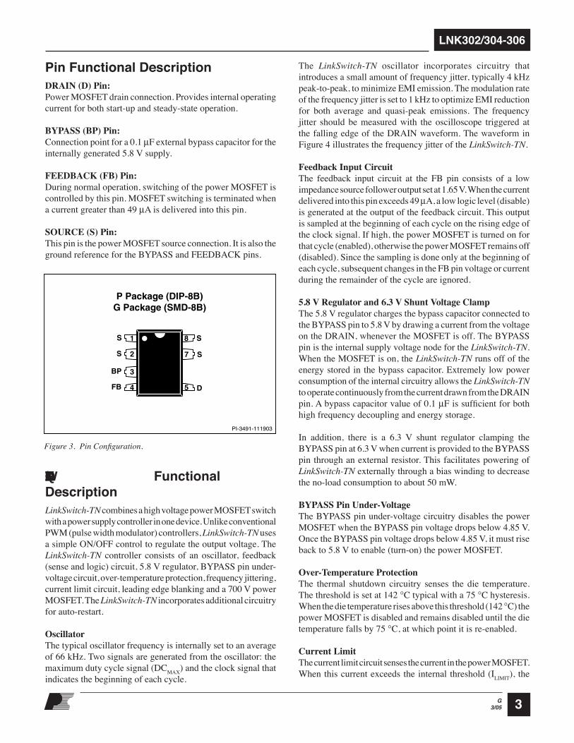
Figure 2b. Functional Block Diagram (LNK304-306).
PI-3904-020805
CLOCKJITTER
OSCILLATOR
5.8 V4.85 V
SOURCE(S)
S
R
Q
DCMAX
BYPASS(BP)
+
- VILIMIT
LEADINGEDGE
BLANKING
THERMALSHUTDOWN
+
-
DRAIN(D)
REGULATOR5.8 V
BYPASS PINUNDER-VOLTAGE
CURRENT LIMITCOMPARATOR
FEEDBACK(FB)
Q
6.3 V
1.65 V -VT
3
LNK302/304-306
G3/05
Pin Functional DescriptionDRAIN (D) Pin:Power MOSFET drain connection. Provides internal operating current for both start-up and steady-state operation.
BYPASS (BP) Pin:Connection point for a 0.1 µF external bypass capacitor for the internally generated 5.8 V supply.
FEEDBACK (FB) Pin:During normal operation, switching of the power MOSFET is controlled by this pin. MOSFET switching is terminated when a current greater than 49 µA is delivered into this pin.
SOURCE (S) Pin:This pin is the power MOSFET source connection. It is also the ground reference for the BYPASS and FEEDBACK pins.
LinkSwitch-TN Functional DescriptionLinkSwitch-TN combines a high voltage power MOSFET switch with a power supply controller in one device. Unlike conventional PWM (pulse width modulator) controllers, LinkSwitch-TN uses a simple ON/OFF control to regulate the output voltage. The LinkSwitch-TN controller consists of an oscillator, feedback (sense and logic) circuit, 5.8 V regulator, BYPASS pin under-voltage circuit, over-temperature protection, frequency jittering, current limit circuit, leading edge blanking and a 700 V power MOSFET. The LinkSwitch-TN incorporates additional circuitry for auto-restart.
OscillatorThe typical oscillator frequency is internally set to an average of 66 kHz. Two signals are generated from the oscillator: the maximum duty cycle signal (DCMAX) and the clock signal that indicates the beginning of each cycle.
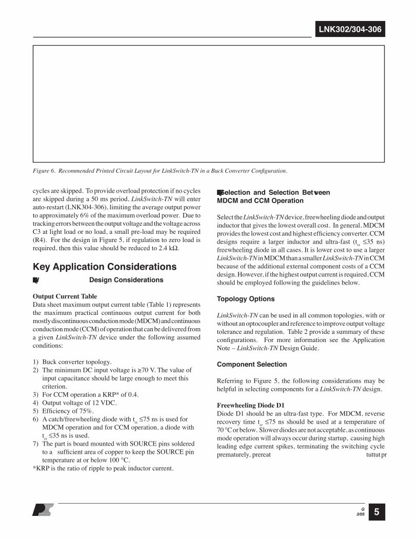
The LinkSwitch-TN oscillator incorporates circuitry that introduces a small amount of frequency jitter, typically 4 kHz peak-to-peak, to minimize EMI emission. The modulation rate of the frequency jitter is set to 1 kHz to optimize EMI reduction for both average and quasi-peak emissions. The frequency jitter should be measured with the oscilloscope triggered at the falling edge of the DRAIN waveform. The waveform in Figure 4 illustrates the frequency jitter of the LinkSwitch-TN.
Feedback Input CircuitThe feedback input circuit at the FB pin consists of a low impedance source follower output set at 1.65 V. When the current delivered into this pin exceeds 49 µA, a low logic level (disable) is generated at the output of the feedback circuit. This output is sampled at the beginning of each cycle on the rising edge of the clock signal. If high, the power MOSFET is turned on for that cycle (enabled), otherwise the power MOSFET remains off (disabled). Since the sampling is done only at the beginning of each cycle, subsequent changes in the FB pin voltage or current during the remainder of the cycle are ignored.
5.8 V Regulator and 6.3 V Shunt Voltage ClampThe 5.8 V regulator charges the bypass capacitor connected to the BYPASS pin to 5.8 V by drawing a current from the voltage on the DRAIN, whenever the MOSFET is off. The BYPASS pin is the internal supply voltage node for the LinkSwitch-TN. When the MOSFET is on, the LinkSwitch-TN runs off of the energy stored in the bypass capacitor. Extremely low power consumption of the internal circuitry allows the LinkSwitch-TN to operate continuously from the current drawn from the DRAIN pin. A bypass capacitor value of 0.1 µF is sufficient for both high frequency decoupling and energy storage.
In addition, there is a 6.3 V shunt regulator clamping the BYPASS pin at 6.3 V when current is provided to the BYPASS pin through an external resistor. This facilitates powering of LinkSwitch-TN externally through a bias winding to decrease the no-load consumption to about 50 mW.
BYPASS Pin Under-VoltageThe BYPASS pin under-voltage circuitry disables the power MOSFET when the BYPASS pin voltage drops below 4.85 V. Once the BYPASS pin voltage drops below 4.85 V, it must rise back to 5.8 V to enable (turn-on) the power MOSFET.
Over-Temperature ProtectionThe thermal shutdown circuitry senses the die temperature. The threshold is set at 142 °C typical with a 75 °C hysteresis. When the die temperature rises above this threshold (142 °C) the power MOSFET is disabled and remains disabled until the die temperature falls by 75 °C, at which point it is re-enabled.
Current LimitThe current limit circuit senses the current in the power MOSFET. When this current exceeds the internal threshold (ILIMIT), the
PI-3491-111903
FB D
S
BP
S
SS
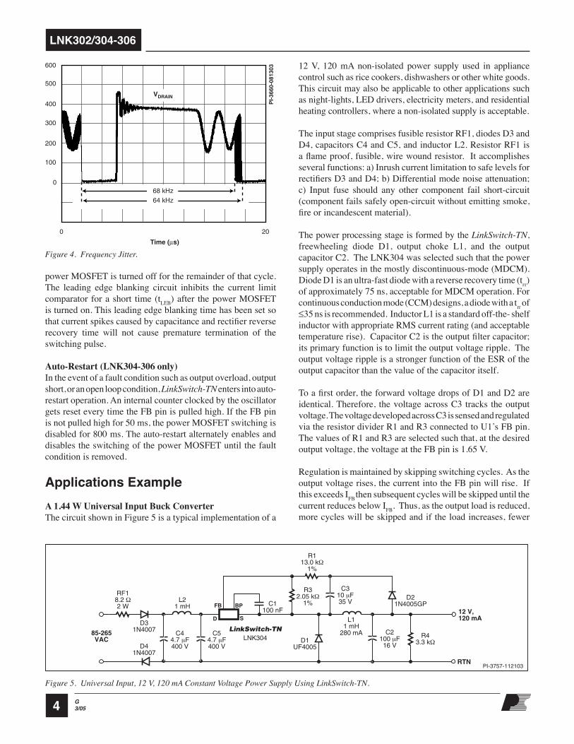
P Package (DIP-8B)G Package (SMD-8B)
8
5
7
1
4
2
3
Figure 3. Pin Configuration.
4
LNK302/304-306
G3/05
Figure 5. Universal Input, 12 V, 120 mA Constant Voltage Power Supply Using LinkSwitch-TN.
power MOSFET is turned off for the remainder of that cycle. The leading edge blanking circuit inhibits the current limit comparator for a short time (tLEB) after the power MOSFET is turned on. This leading edge blanking time has been set so that current spikes caused by capacitance and rectifier reverse recovery time will not cause premature termination of the switching pulse.
Auto-Restart (LNK304-306 only)In the event of a fault condition such as output overload, output short, or an open loop condition, LinkSwitch-TN enters into auto-restart operation. An internal counter clocked by the oscillator gets reset every time the FB pin is pulled high. If the FB pin is not pulled high for 50 ms, the power MOSFET switching is disabled for 800 ms. The auto-restart alternately enables and disables the switching of the power MOSFET until the fault condition is removed.
Applications ExampleA 1.44 W Universal Input Buck ConverterThe circuit shown in Figure 5 is a typical implementation of a
Figure 4. Frequency Jitter.
RTN
12 V,120 mA
85-265VAC
PI-3757-112103
FB BP
SD
LinkSwitch-TNC4
4.7 µF400 V
C1100 nF
D41N4007
D31N4007
D1UF4005
LNK304
D21N4005GP
C2100 µF16 V
RF18.2 Ω2 W
R113.0 kΩ
1%
R32.05 kΩ
1%L21 mH
L11 mH
280 mAC54.7 µF400 V
C310 µF35 V
R43.3 kΩ
12 V, 120 mA non-isolated power supply used in appliance control such as rice cookers, dishwashers or other white goods. This circuit may also be applicable to other applications such as night-lights, LED drivers, electricity meters, and residential heating controllers, where a non-isolated supply is acceptable.
The input stage comprises fusible resistor RF1, diodes D3 and D4, capacitors C4 and C5, and inductor L2. Resistor RF1 is a flame proof, fusible, wire wound resistor. It accomplishes several functions: a) Inrush current limitation to safe levels for rectifiers D3 and D4; b) Differential mode noise attenuation; c) Input fuse should any other component fail short-circuit (component fails safely open-circuit without emitting smoke, fire or incandescent material).
The power processing stage is formed by the LinkSwitch-TN, freewheeling diode D1, output choke L1, and the output capacitor C2. The LNK304 was selected such that the power supply operates in the mostly discontinuous-mode (MDCM). Diode D1 is an ultra-fast diode with a reverse recovery time (trr) of approximately 75 ns, acceptable for MDCM operation. For continuous conduction mode (CCM) designs, a diode with a trr of ≤35 ns is recommended. Inductor L1 is a standard off-the- shelf inductor with appropriate RMS current rating (and acceptable temperature rise). Capacitor C2 is the output filter capacitor; its primary function is to limit the output voltage ripple. The output voltage ripple is a stronger function of the ESR of the output capacitor than the value of the capacitor itself.
To a first order, the forward voltage drops of D1 and D2 are identical. Therefore, the voltage across C3 tracks the output voltage. The voltage developed across C3 is sensed and regulated via the resistor divider R1 and R3 connected to U1ʼs FB pin. The values of R1 and R3 are selected such that, at the desired output voltage, the voltage at the FB pin is 1.65 V.
Regulation is maintained by skipping switching cycles. As the output voltage rises, the current into the FB pin will rise. If this exceeds IFB then subsequent cycles will be skipped until the current reduces below IFB. Thus, as the output load is reduced, more cycles will be skipped and if the load increases, fewer
600
0 20
68 kHz64 kHz
VDRAIN
Time (µs)
PI-
3660
-081
303
500
400
300
200
100
0
6
LNK302/304-306
G3/05
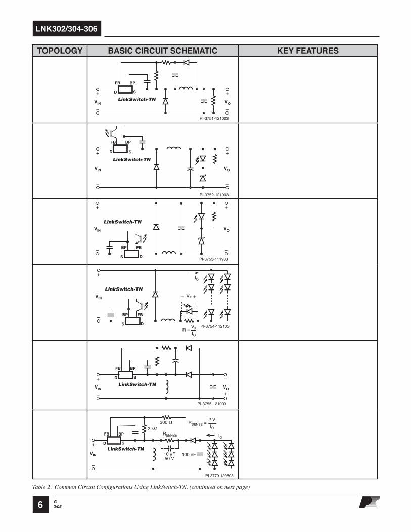
Table 2. Common Circuit Configurations Using LinkSwitch-TN. (continued on next page)
TOPOLOGY BASIC CIRCUIT SCHEMATIC KEY FEATURESHigh-Side Buck ð Direct Feedback
1. Output referenced to input 2. Positive output (VO) with respect to -VIN 3. Step down ð VO < VIN 4. Low cost direct feedback (Ñ10% typ.)
High-Side Buck ð Optocoupler Feedback
1. Output referenced to input 2. Positive output (VO) with respect to -VIN 3. Step down ð VO < VIN 4. Optocoupler feedback - Accuracy only limited by reference choice - Low cost non-safety rated opto - No pre-load required 5. Minimum no-load consumption
Low-Side Buck ð Optocoupler Feedback
1. Output referenced to input 2. Negative output (VO) with respect to +VIN 3. Step down ð VO < VIN 4. Optocoupler feedback - Accuracy only limited by reference choice - Low cost non-safety rated opto - No pre-load required - Ideal for driving LEDs
Low-Side Buck ð Constant Current LED Driver
High-Side Buck Boost ð Direct Feedback
1. Output referenced to input 2. Negative output (VO) with respect to +VIN 3. Step up/down ð VO > VIN or VO < VIN 4. Low cost direct feedback (Ñ10% typ.) 5. Fail-safe ð output is not subjected to input voltage if the internal MOSFET fails 6. Ideal for driving LEDs ð better accuracy and temperature stability than Low-side Buck constant current LED driver
High-Side Buck Boost ð Constant Current LED Driver
VOVIN
PI-3751-121003
+ +
FB BP
SD
LinkSwitch-TN
LinkSwitch-TN
PI-3752-121003
+ +
BPFB
D S
VOVIN
LinkSwitch-TN
PI-3753-111903
+ +
BP FB
DS
VOVIN
LinkSwitch-TN
PI-3754-112103
+
+
BP FB
DS
VIN
IO
R =
VF
VF
IO
VOVIN
PI-3755-121003
+
+
FB BP
SD
LinkSwitch-TN
RSENSE =
RSENSE
300 Ω2 kΩ
2 V
IO
IO
100 nF10 µF50 V
VIN
PI-3779-120803
+
FB BP
SD
LinkSwitch-TN
8
LNK302/304-306
G3/05
be included for better EMI performance and higher line surge withstand capability.
Quick Design Checklist
As with any power supply design, all LinkSwitch-TN designs should be verified for proper functionality on the bench. The following minimum tests are recommended:
1) Adequate DC rail voltage – check that the minimum DC input voltage does not fall below 70 VDC at maximum load, minimum input voltage.
2) Correct Diode Selection – UF400x series diodes are recommended only for designs that operate in MDCM at an ambient of 70 °C or below. For designs operating in continuous conduction mode (CCM) and/or higher ambients, then a diode with a reverse recovery time of 35 ns or better, such as the BYV26C, is recommended.
3) Maximum drain current – verify that the peak drain current is below the data sheet peak drain specification under
worst-case conditions of highest line voltage, maximum overload (just prior to auto-restart) and highest ambient temperature.
4) Thermal check – at maximum output power, minimum input voltage and maximum ambient temperature, verify that the LinkSwitch-TN SOURCE pin temperature is 100 °C or below. This figure ensures adequate margin due to variations in RDS(ON) from part to part. A battery powered thermocouple meter is recommended to make measurements when the SOURCE pins are a switching node. Alternatively, the ambient temperature may be raised to indicate margin to thermal shutdown.
In a LinkSwitch-TN design using a buck or buck boost converter topology, the SOURCE pin is a switching node. Oscilloscope measurements should therefore be made with probe grounded to a DC voltage, such as primary return or DC input rail, and not to the SOURCE pins. The power supply input must always be supplied from an isolated source (e.g. via an isolation transformer).
9
LNK302/304-306
G3/05
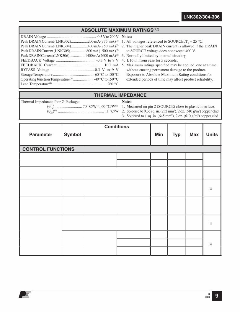
ABSOLUTE MAXIMUM RATINGS(1,5)
DRAIN Voltage .................................. ................ -0.3 V to 700 V Peak DRAIN Current (LNK302).................200 mA (375 mA)(2) Peak DRAIN Current (LNK304).................400 mA (750 mA)(2) Peak DRAIN Current (LNK305).................800 mA (1500 mA)(2) Peak DRAIN Current (LNK306).................1400 mA (2600 mA)(2) FEEDBACK Voltage .........................................-0.3 V to 9 V FEEDBACK Current.............................................100 mA BYPASS Voltage ..........................................-0.3 V to 9 V Storage Temperature .......................................... -65 °C to 150 °C Operating Junction Temperature(3) ..................... -40 °C to 150 °C Lead Temperature(4) ........................................................260 °C
Notes: 1. All voltages referenced to SOURCE, TA = 25 °C. 2. The higher peak DRAIN current is allowed if the DRAIN to SOURCE voltage does not exceed 400 V. 3. Normally limited by internal circuitry. 4. 1/16 in. from case for 5 seconds. 5. Maximum ratings specified may be applied, one at a time, without causing permanent damage to the product. Exposure to Absolute Maximum Rating conditions for extended periods of time may affect product reliability.
THERMAL IMPEDANCEThermal Impedance: P or G Package: (θJA) ........................... 70 °C/W(2); 60 °C/W(3)
(θJC)(1) ............................................... 11 °C/W
Notes: 1. Measured on pin 2 (SOURCE) close to plastic interface. 2. Soldered to 0.36 sq. in. (232 mm2), 2 oz. (610 g/m2) copper clad. 3. Soldered to 1 sq. in. (645 mm2), 2 oz. (610 g/m2) copper clad.
Parameter SymbolConditions
SOURCE = 0 V; TJ = -40 to 125 ÁC See Figure 7
(Unless Otherwise Speciþed)
Min Typ Max Units
CONTROL FUNCTIONSOutput Frequency fOSC TJ = 25 ÁC
Average 62 66 70kHz
Peak-Peak Jitter 4
Maximum Duty Cycle DCMAX S2 Open 66 69 72 %
FEEDBACK Pin Turnoff Threshold Current
IFB TJ = 25 ÁC 30 49 68 µA
FEEDBACK Pin Voltage at Turnoff Threshold
VFB 1.54 1.65 1.76 V
DRAIN Supply Current
IS1VFB Ó2 V
(MOSFET Not Switching) See Note A
160 220 µA
IS2
FEEDBACK Open
(MOSFET Switching)
See Notes A, B
LNK302/304 200 260
µALNK305 220 280
LNK306 250 310
10
LNK302/304-306
G3/05
Parameter Symbol
Con
SOURCE = 0 V; T
J
= -40 to 125 ÁC
See Figure 7
(UnӏᵀᵀMᵐӿӏᴰᶀԏᵀӏMήᴐӏүԏ ed)
Min Typ
Max
Un
CONTROL FUNCTIONS (conĔfi
BYPASS Pin
Charge Currenᵐ
I
CH1
V
BP
= 0 V
T
J
= 25 ÁC
LNK302/304
-5.5 -3.3 -1.8
mA LNK305/306
-7.5 -4.6 -2.5
I
CH2
V
BP
= 4 V
T
J
= 25 ÁC
LNK302/304
-3.8 -2.3 -1.0
LNK305/306
-4.5 -3.3 -1.5
BYPASS Pin VoltageV
BP
5.55 5.8
6.10
V
BYPASS Pin Voltage HysteresisV
BPH
0.8 0.95 1.2 V
BYPASS Pin Supply Current
I
BPSC
See Note D 68 µA
CIRCUIT PROTECTION
Current LimitI
LIMIT
(See Note E)
di/dt = 55 mA/
µ
s TJ = 25 °
C
LNK302
126 136146
mA
di/dt = 250 mA/ µs
T
J
= 25 °
C
145 165185
di/dt = 65 mA/
µ
s TJ = 25 °
C
LNK304
240 257275
di/dt = 415 mA/ µs TJ = 25 °
C
271 308345
di/dt = 75 mA/
µ
s TJ = 25 °
C
LNK305
350 375401
di/dt = 500 mA/ µs TJ = 25 °
C
396 450504
di/dt = 95 mA/
µ
s TJ = 25 °
C
LNK306
450 482515
di/dt = 610 mA/ µs TJ = 25 °
C
508 578647
Minimum On Time t
ON(MIN)
LNK302/304 280 360475
ns
LNK305 360 460610
LNK306 400 500675
11
LNK302/304-306
G3/05
Parameter SymbolConditions
SOURCE = 0 V; TJ = -40 to 125 ÁC See Figure 7
(Unless Otherwise Speciþed)
Min Typ Max Units
CIRCUIT PROTECTION (cont.)Leading Edge Blanking Time tLEB
TJ = 25 °C See Note F 170 215 ns
Thermal Shutdown Temperature TSD 135 142 150 °C
Thermal Shutdown Hysteresis TSHD See Note G 75 °C
OUTPUT
ON-State Resistance RDS(ON)
LNK302 ID = 13 mA
TJ = 25 °C 48 55.2
Ω
TJ = 100 °C 76 88.4
LNK304 ID = 25 mA
TJ = 25 °C 24 27.6TJ = 100 °C 38 44.2
LNK305 ID = 35 mA
TJ = 25 °C 12 13.8TJ = 100 °C 19 22.1
LNK306 ID = 45 mA
TJ = 25 °C 7 8.1TJ = 100 °C 11 12.9
OFF-State Drain Leakage Current IDSS
VBP = 6.2 V, VFB Ó2 V, VDS = 560 V, TJ = 25 °C
LNK302/304 50
µALNK305 70
LNK306 90
Breakdown Voltage BVDSSVBP = 6.2 V, VFB Ó2 V,
TJ = 25 °C700 V
Rise Time tR Measured in a Typical Buck Converter Application
50 ns
Fall Time tF 50 ns
DRAIN Supply Voltage 50 V
Output Enable Delay tEN See Figure 9 10 µs
Output Disable Setup Time tDST 0.5 µs
Auto-Restart ON-Time tAR
TJ = 25 °C See Note H
LNK302ms
LNK304-306 50
Auto-Restart Duty Cycle DCAR
LNK302%
LNK304-306 6
Not Applicable
Not Applicable
12
LNK302/304-306
G3/05
NOTES:A. Total current consumption is the sum of IS1 and IDSS when FEEDBACK pin voltage is Ó2 V (MOSFET not
switching) and the sum of IS2 and IDSS when FEEDBACK pin is shorted to SOURCE (MOSFET switching).
B Since the output MOSFET is switching, it is difþcult to isolate the switching current from the supply current at the DRAIN. An alternative is to measure the BYPASS pin current at 6 V.
C. See Typical Performance Characteristics section Figure 14 for BYPASS pin start-up charging waveform.
D. This current is only intended to supply an optional optocoupler connected between the BYPASS and FEEDBACK pins and not any other external circuitry.
E. For current limit at other di/dt values, refer to Figure 13.
F. This parameter is guaranteed by design.
G. This parameter is derived from characterization.
H. Auto-restart on time has the same temperature characteristics as the oscillator (inversely proportional to frequency).
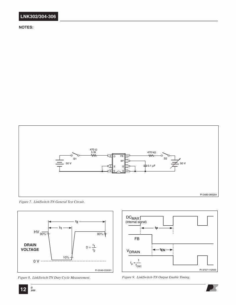
Figure 7. LinkSwitch-TN General Test Circuit.
PI-3490-060204
50 V50 V
D FB
SS
S S
BPS1
470 kΩ
S2
0.1 µF
470 Ω5 W
PI-3707-112503
FB
tP
tEN
DCMAX
tP =
1
fOSC
VDRAIN
(internal signal)
Figure 8. LinkSwitch-TN Duty Cycle Measurement. Figure 9. LinkSwitch-TN Output Enable Timing.
13
LNK302/304-306
G3/05
200
300
350
400
250
00 42 86 10 12 14 16 18 20
DRAIN Voltage (V)
DR
AIN
Cu
rren
t (m
A) PI-
3661
-071
404
50
150
100
Scaling Factors:LNK302 0.5LNK304 1.0LNK305 2.0LNK306 3.4
25 °C100 °C
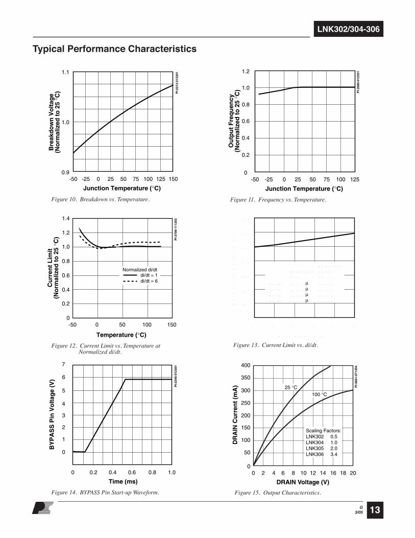
Typical Performance Characteristics
Figure 14. BYPASS Pin Start-up Waveform.
1.1
1.0
0.9-50 -25 0 25 50 75 100 125 150
Junction Temperature (°C)
Bre
akd
ow
n V
olt
age
(No
rmal
ized
to
25
°C) PI-
2213
-012
301
6
5
4
3
2
1
0
0 0.2 0.4 0.6 0.8 1.0
Time (ms)
PI-
2240
-012
301
BY
PA
SS
Pin
Vo
ltag
e (V
)
7
Figure 10. Breakdown vs. Temperature.
Figure 12. Current Limit vs. Temperature at Normalized di/dt.
Figure 13. Current Limit vs. di/dt.
Figure 15. Output Characteristics.
1.2
1.0
0.8
0.6
0.4
0.2
0-50 -25 0 25 50 75 100 125
Junction Temperature (°C)
PI-
2680
-012
301
Ou
tpu
t F
req
uen
cy(N
orm
aliz
ed t
o 2
5 °C
)
Figure 11. Frequency vs. Temperature.
Normalized di/dt
PI-
3710
-071
204
No
rmal
ized
Cu
rren
t L
imit
1.0
1.2
1.4
0.8
0.6
0.4
0.2
01 2 3 4 5 6
LNK302LNK304LNK305LNK306
Normalized di/dt = 155 mA/µs65 mA/µs75 mA/µs95 mA/µs
Normalized CurrentLimit = 1136 mA257 mA375 mA482 mA
Temperature (°C)
PI-
3709
-111
203
Cu
rren
t L
imit
(No
rmal
ized
to
25
°C)
1.0
1.2
1.4
0.8
0.6
0.4
0.2
0-50 0 50 100 150
di/dt = 1di/dt = 6
Normalized di/dt
14
LNK302/304-306
G3/05
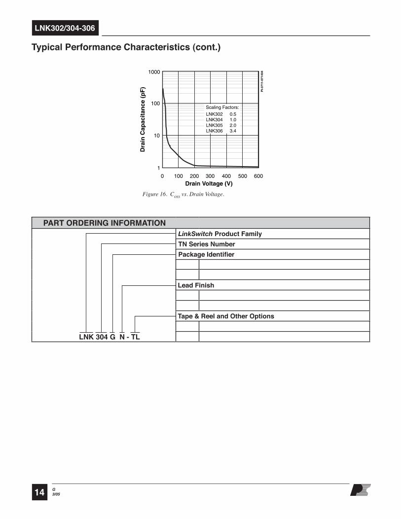
Figure 16. COSS vs. Drain Voltage.
Drain Voltage (V)
Dra
in C
apac
itan
ce (
pF
)
PI-
3711
-071
404
0 100 200 300 400 500 600
1
10
100
1000
LNK302 0.5LNK304 1.0LNK305 2.0LNK306 3.4
Scaling Factors:
Typical Performance Characteristics (cont.)
PART ORDERING INFORMATIONLinkSwitch Product FamilyTN Series NumberPackage IdentifierG Plastic Surface Mount DIPP Plastic DIP
Lead FinishBlank Standard (Sn Pb)N Pure Matte Tin (Pb-Free)
Tape & Reel and Other OptionsBlank Standard ConþgurationsTL Tape & Reel, 1 k pcs minimum, G Package onlyLNK 304 G N - TL
15
LNK302/304-306
G3/05
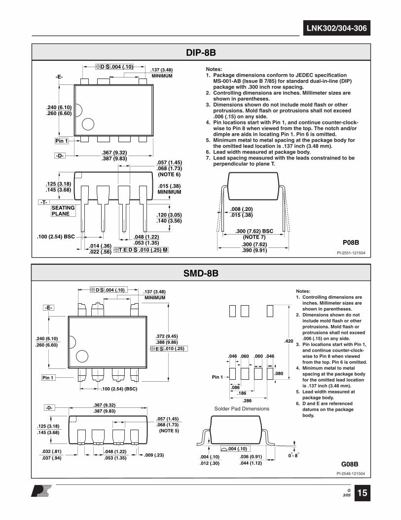
Notes:1. Package dimensions conform to JEDEC specification MS-001-AB (Issue B 7/85) for standard dual-in-line (DIP) package with .300 inch row spacing.2. Controlling dimensions are inches. Millimeter sizes are shown in parentheses.3. Dimensions shown do not include mold flash or other protrusions. Mold flash or protrusions shall not exceed .006 (.15) on any side.4. Pin locations start with Pin 1, and continue counter-clock- wise to Pin 8 when viewed from the top. The notch and/or dimple are aids in locating Pin 1. Pin 6 is omitted.5. Minimum metal to metal spacing at the package body for the omitted lead location is .137 inch (3.48 mm).6. Lead width measured at package body. 7. Lead spacing measured with the leads constrained to be perpendicular to plane T.
.008 (.20)
.015 (.38)
.300 (7.62) BSC(NOTE 7)
.300 (7.62)
.390 (9.91)
.367 (9.32)
.387 (9.83)
.240 (6.10)
.260 (6.60)
.125 (3.18)
.145 (3.68)
.057 (1.45)
.068 (1.73)
.120 (3.05)
.140 (3.56)
.015 (.38)MINIMUM
.048 (1.22)
.053 (1.35).100 (2.54) BSC
.014 (.36)
.022 (.56)
-E-
Pin 1
SEATINGPLANE
-D-
-T-
P08B
DIP-8B
PI-2551-121504
D S .004 (.10)⊕
T E D S .010 (.25) M⊕
(NOTE 6)
.137 (3.48) MINIMUM
SMD-8B
PI-2546-121504
.004 (.10)
.012 (.30).036 (0.91).044 (1.12)
.004 (.10)
0 - ° 8°
.367 (9.32)
.387 (9.83)
.048 (1.22).009 (.23)
.053 (1.35).032 (.81).037 (.94)
.125 (3.18)
.145 (3.68)
-D-
Notes:1. Controlling dimensions are inches. Millimeter sizes are shown in parentheses.2. Dimensions shown do not include mold flash or other protrusions. Mold flash or protrusions shall not exceed .006 (.15) on any side.3. Pin locations start with Pin 1, and continue counter-clock- wise to Pin 8 when viewed from the top. Pin 6 is omitted.4. Minimum metal to metal spacing at the package body for the omitted lead location is .137 inch (3.48 mm).5. Lead width measured at package body. 6. D and E are referenced datums on the package body.
.057 (1.45)
.068 (1.73)(NOTE 5)
E S
.100 (2.54) (BSC)
.372 (9.45).240 (6.10)
.388 (9.86)
.137 (3.48) MINIMUM
.260 (6.60).010 (.25)
-E-
Pin 1
D S .004 (.10)⊕
⊕
G08B
.420
.046 .060 .060 .046
.080Pin 1
.086.186
.286
Solder Pad Dimensions

16
LNK302/304-306
G3/05
Revision Notes DateC 1) Released Final Data Sheet. 3/03D 1) Corrected Minimum On Time. 1/04E 1) Added LNK302. 8/04F 1) Added lead-free ordering information. 12/04G 1) Minor error corrections.
2) Renamed Feedback Pin Voltage parameter to Feedback Pin Voltage at Turnoff Threshold and removed condition.
3/05
For the latest updates, visit our website: www.powerint.comPower Integrations reserves the right to make changes to its products at any time to improve reliability or manufacturability. Power Integrations does not assume any liability arising from the use of any device or circuit described herein. POWER INTEGRATIONS MAKES NO WARRANTY HEREIN AND SPECIFICALLY DISCLAIMS ALL WARRANTIES INCLUDING, WITHOUT LIMITATION, THE IMPLIED WARRANTIES OF MERCHANTABILITY, FITNESS FOR A PARTICULAR PURPOSE, AND NON-INFRINGEMENT OF THIRD PARTY RIGHTS.
PATENT INFORMATION
The products and applications illustrated herein (including transformer construction and circuits external to the products) may be covered by one or more U.S. and foreign patents, or potentially by pending U.S. and foreign patent applications assigned to Power Integrations. A complete list of Power Integrations patents may be found at www.powerint.com. Power Integrations grants its customers a license under certain patent rights as set forth at http://www.powerint.com/ip.htm.
LIFE SUPPORT POLICY
POWER INTEGRATIONS PRODUCTS ARE NOT AUTHORIZED FOR USE AS CRITICAL COMPONENTS IN LIFE SUPPORT DEVICES OR SYSTEMS WITHOUT THE EXPRESS WRITTEN APPROVAL OF THE PRESIDENT OF POWER INTEGRATIONS. As used herein:
1. A Life support device or system is one which, (i) is intended for surgical implant into the body, or (ii) supports or sustains life, and (iii) whose failure to perform, when properly used in accordance with instructions for use, can be reasonably expected to result in significant injury or death to the user.
2. A critical component is any component of a life support device or system whose failure to perform can be reasonably expected to cause the failure of the life support device or system, or to affect its safety or effectiveness.
The PI logo, TOPSwitch, TinySwitch, LinkSwitch, DPA-Switch, EcoSmart, PI Expert and PI FACTS are trademarks of Power Integrations, Inc. Other trademarks are property of their respective companies. ©Copyright 2005, Power Integrations, Inc.
Power Integrations Worldwide Sales Support Locations
Mil :
Laip:
aip:
aip:
aip: 2V-OC T7Teb Aip: bPAip: Aip: Aip: Aip: Aip:


![HOG BUNG DROPPER - Kentmaster · rev b: 08/10 operator’s manual [english]: hog bung dropper including: operation, instruction, installation and maintenance important: read this](https://img.pdfslide.us/doc/110x75/5b4789b27f8b9a5e5f8c2eeb/hog-bung-dropper-rev-b-0810-operators-manual-english-hog-bung-dropper.jpg)