Embed Size (px)
Citation preview

See discussions, stats, and author profiles for this publication at: https://www.researchgate.net/publication/290738190
Analysis and filter design of differential mode EMI noise for GaN-based
interleaved MHz critical mode PFC converter
Article · November 2014
DOI: 10.1109/ECCE.2014.6954056
CITATIONS
17
READS
96
4 authors, including:
Some of the authors of this publication are also working on these related projects:
WBG-Based On-Board Charger View project
High-performance DC/DC Converters for Future Data Center Power Supplies View project
Yuchen Yang
Virginia Polytechnic Institute and State University
14 PUBLICATIONS 186 CITATIONS
SEE PROFILE
Zhengyang Liu
Virginia Polytechnic Institute and State University
34 PUBLICATIONS 740 CITATIONS
SEE PROFILE
F.C.Y. Lee
Virginia Polytechnic Institute and State University
1,078 PUBLICATIONS 39,467 CITATIONS
SEE PROFILE
All content following this page was uploaded by Zhengyang Liu on 25 August 2016.
The user has requested enhancement of the downloaded file.
Analysis and Filter Design of Differential Mode
EMI Noise for GaN-based Interleaved MHz
Critical Mode PFC Converter
Yuchen Yang, Zhengyang Liu, Fred C. Lee and Qiang Li
Center for Power Electronics Systems
The Bradley Department of Electrical and Computer Engineering
Virginia Tech, Blacksburg, VA 24061 USA
Abstract—Power factor correction (PFC) converter
consumes a large part of volume of power supply. Typical
switching frequency of commercial PFC converter is usually not
higher than several hundred kHz. Increasing the switching
frequency of PFC converter to MHz by using GaN devices can
greatly reduce the size and increase power density of power
supply. In order to eliminate the high turn-on loss of cascode
GaN device, critical conduction mode (CRM) is applied.
However, when operating on CRM, PFC converter has large
inductor current ripple and variable switching frequency. This
makes the differential mode (DM) noise a serious issue for CRM
PFC converter. This paper provides a more accurate model to
calculate the switching frequency and DM noise of MHz CRM
PFC converter. Based on the model and experiment result,
interleaving impact of DM noise for MHz CRM PFC converter
is analyzed. DM noise filter is designed and it demonstrates that
increasing the switching frequency of PFC converter to MHz
can greatly increase the corner frequency of DM filter and
reduce the filter size significantly.
I. INTRODUCTION
Power factor correction (PFC) converter is a very essential
component of power supply. In commercial products, the
switching frequency of PFC converter is usually lower than
hundreds of kHz. PFC converter consumes approximately one
third volume of power supply. Increasing the switching
frequency can reduce the volume of PFC converter.
Furthermore, increasing the switching frequency to MHz can
greatly raising the corner frequency of EMI filter and reduce
the filter size. Thus, the power density of power supply can be
increased a lot.
However, MHz switching frequency can introduce great
amount of switching loss. In order to overcome the high turn-
on loss of cascode GaN device, critical conduction mode
(CRM) is a preferred control method. In addition, CRM boost
PFC converter can eliminate the reverse recovery loss of
power diode with ZCS. The other advantages of CRM boost
PFC converter are high power factor and smaller peak
inductor current [1-3].
The operation principle of CRM boost PFC converter is
well known. When the inductor current touches zero, the
switch turns on. After a fixed on-time, the switch turns off.
Hence, the peak current of inductor follows the equation
below.
𝑖𝑝𝑘 =𝑉𝑖𝑛
𝐿𝑇𝑜𝑛 (1)
As long as Ton is fixed, the peak current of inductor follows
Vin. Theoretically, the waveform of inductor current is a series
of triangle waveform with maximum value described in
Equation (1) and minimum value as zero. Thus, the average
inductor current is always half of the peak inductor current,
which means that CRM PFC converter can automatically
achieve high power factor. Furthermore the switching
frequency can be calculated.
𝑓𝑠(𝑡) =𝑉𝑖𝑛𝑅𝑀𝑆2 (𝑉𝑂−√2𝑉𝑖𝑛𝑅𝑀𝑆
sin(𝜔𝑡))
2𝐿𝑃𝑂𝑉𝑂 (2)
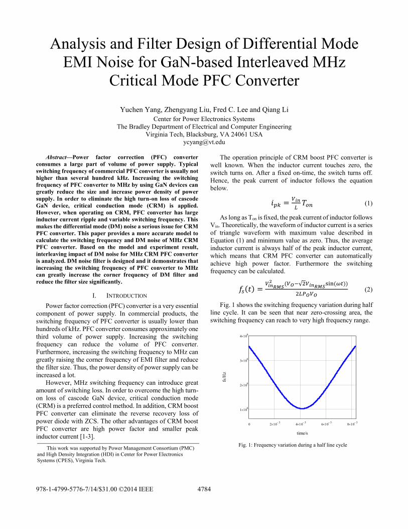
Fig. 1 shows the switching frequency variation during half
line cycle. It can be seen that near zero-crossing area, the
switching frequency can reach to very high frequency range.
This work was supported by Power Management Consortium (PMC)
and High Density Integration (HDI) in Center for Power Electronics Systems (CPES), Virginia Tech.
Fig. 1: Frequency variation during a half line cycle
0 2 103
4 103
6 103
8 103
1 106
2 106
3 106
4 106
time/s
fs/H
z
978-1-4799-5776-7/14/$31.00 ©2014 IEEE 4784
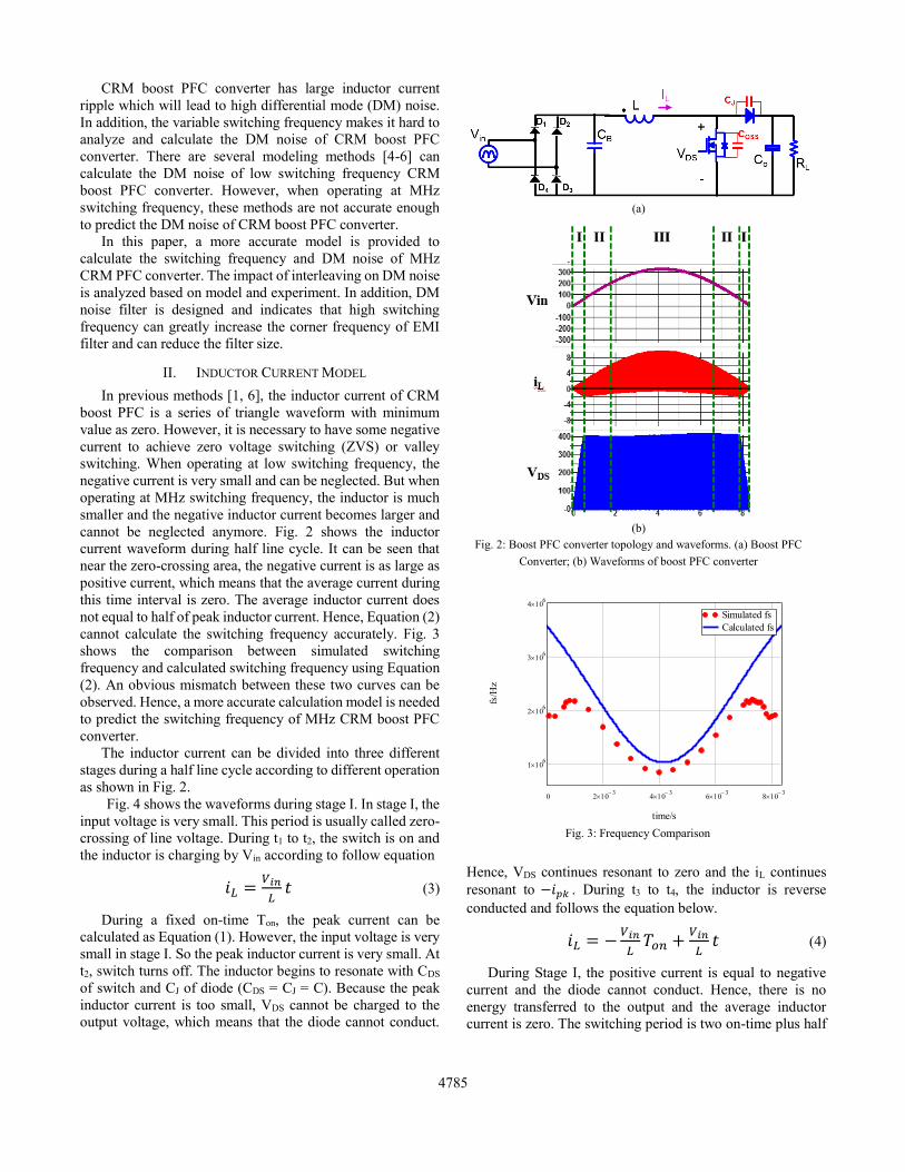
CRM boost PFC converter has large inductor current
ripple which will lead to high differential mode (DM) noise.
In addition, the variable switching frequency makes it hard to
analyze and calculate the DM noise of CRM boost PFC
converter. There are several modeling methods [4-6] can
calculate the DM noise of low switching frequency CRM
boost PFC converter. However, when operating at MHz
switching frequency, these methods are not accurate enough
to predict the DM noise of CRM boost PFC converter.
In this paper, a more accurate model is provided to
calculate the switching frequency and DM noise of MHz
CRM PFC converter. The impact of interleaving on DM noise
is analyzed based on model and experiment. In addition, DM
noise filter is designed and indicates that high switching
frequency can greatly increase the corner frequency of EMI
filter and can reduce the filter size.
II. INDUCTOR CURRENT MODEL
In previous methods [1, 6], the inductor current of CRM
boost PFC is a series of triangle waveform with minimum
value as zero. However, it is necessary to have some negative
current to achieve zero voltage switching (ZVS) or valley
switching. When operating at low switching frequency, the
negative current is very small and can be neglected. But when
operating at MHz switching frequency, the inductor is much
smaller and the negative inductor current becomes larger and
cannot be neglected anymore. Fig. 2 shows the inductor
current waveform during half line cycle. It can be seen that
near the zero-crossing area, the negative current is as large as
positive current, which means that the average current during
this time interval is zero. The average inductor current does
not equal to half of peak inductor current. Hence, Equation (2)
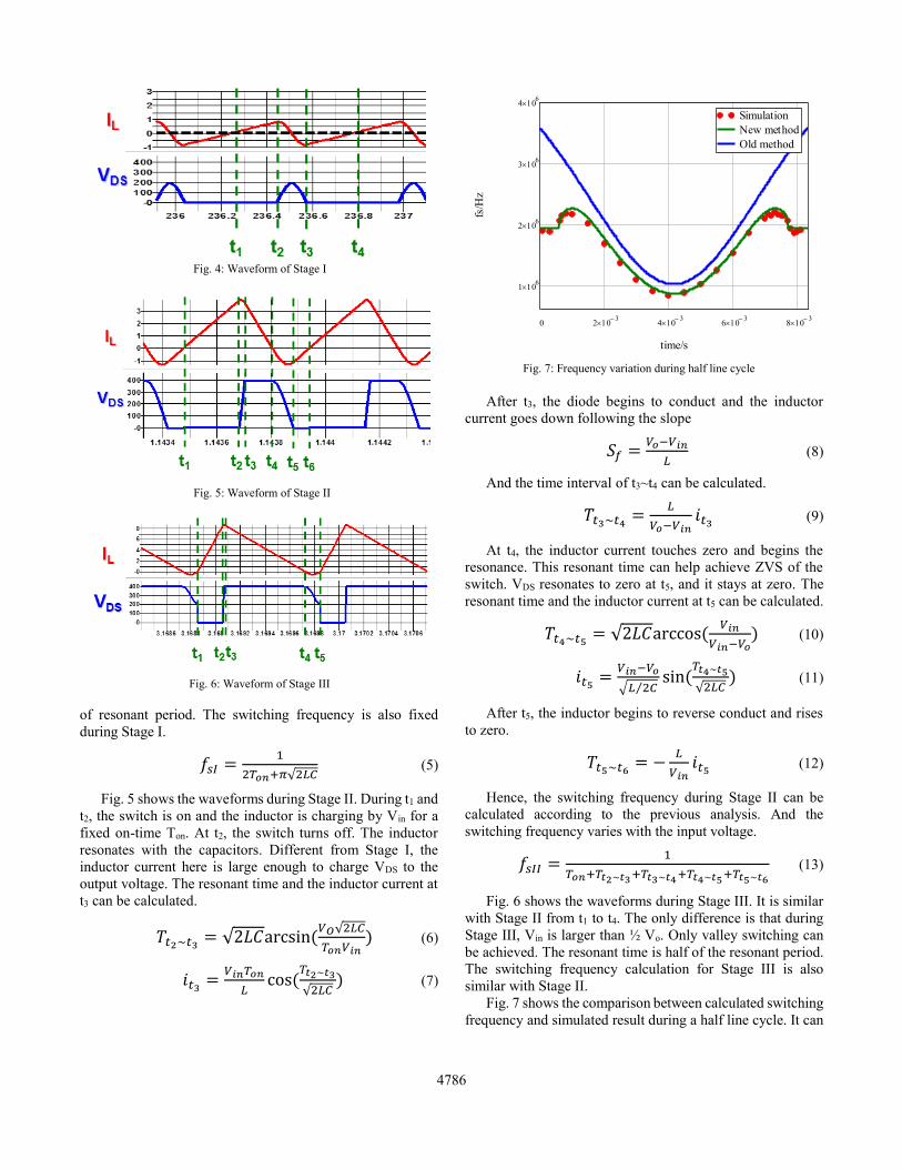
cannot calculate the switching frequency accurately. Fig. 3
shows the comparison between simulated switching
frequency and calculated switching frequency using Equation
(2). An obvious mismatch between these two curves can be
observed. Hence, a more accurate calculation model is needed
to predict the switching frequency of MHz CRM boost PFC
converter.
The inductor current can be divided into three different
stages during a half line cycle according to different operation
as shown in Fig. 2.
Fig. 4 shows the waveforms during stage I. In stage I, the
input voltage is very small. This period is usually called zero-
crossing of line voltage. During t1 to t2, the switch is on and
the inductor is charging by Vin according to follow equation
𝑖𝐿 =𝑉𝑖𝑛
𝐿𝑡 (3)
During a fixed on-time Ton, the peak current can be
calculated as Equation (1). However, the input voltage is very
small in stage I. So the peak inductor current is very small. At
t2, switch turns off. The inductor begins to resonate with CDS
of switch and CJ of diode (CDS = CJ = C). Because the peak
inductor current is too small, VDS cannot be charged to the
output voltage, which means that the diode cannot conduct.
Hence, VDS continues resonant to zero and the iL continues
resonant to −𝑖𝑝𝑘 . During t3 to t4, the inductor is reverse
conducted and follows the equation below.
𝑖𝐿 = −𝑉𝑖𝑛
𝐿𝑇𝑜𝑛 +
𝑉𝑖𝑛
𝐿𝑡 (4)
During Stage I, the positive current is equal to negative
current and the diode cannot conduct. Hence, there is no
energy transferred to the output and the average inductor
current is zero. The switching period is two on-time plus half
(a)
(b)
Fig. 2: Boost PFC converter topology and waveforms. (a) Boost PFC
Converter; (b) Waveforms of boost PFC converter
Fig. 3: Frequency Comparison
0 2 103
4 103
6 103
8 103
1 106
2 106
3 106
4 106
Simulated fs
Calculated fs
time/s
fs/H
z
4785
of resonant period. The switching frequency is also fixed
during Stage I.
𝑓𝑠𝐼 =1
2𝑇𝑜𝑛+𝜋√2𝐿𝐶 (5)
Fig. 5 shows the waveforms during Stage II. During t1 and
t2, the switch is on and the inductor is charging by Vin for a
fixed on-time Ton. At t2, the switch turns off. The inductor
resonates with the capacitors. Different from Stage I, the
inductor current here is large enough to charge VDS to the
output voltage. The resonant time and the inductor current at
t3 can be calculated.
𝑇𝑡2~𝑡3 = √2𝐿𝐶arcsin(𝑉𝑂√2𝐿𝐶
𝑇𝑜𝑛𝑉𝑖𝑛) (6)
𝑖𝑡3 =𝑉𝑖𝑛𝑇𝑜𝑛
𝐿cos(
𝑇𝑡2~𝑡3
√2𝐿𝐶) (7)
After t3, the diode begins to conduct and the inductor
current goes down following the slope
𝑆𝑓 =𝑉𝑜−𝑉𝑖𝑛
𝐿 (8)
And the time interval of t3~t4 can be calculated.
𝑇𝑡3~𝑡4 =𝐿
𝑉𝑜−𝑉𝑖𝑛𝑖𝑡3 (9)
At t4, the inductor current touches zero and begins the
resonance. This resonant time can help achieve ZVS of the
switch. VDS resonates to zero at t5, and it stays at zero. The
resonant time and the inductor current at t5 can be calculated.
𝑇𝑡4~𝑡5 = √2𝐿𝐶arccos(𝑉𝑖𝑛
𝑉𝑖𝑛−𝑉𝑜) (10)
𝑖𝑡5 =𝑉𝑖𝑛−𝑉𝑜
√𝐿 2𝐶⁄sin(
𝑇𝑡4~𝑡5
√2𝐿𝐶) (11)
After t5, the inductor begins to reverse conduct and rises
to zero.
𝑇𝑡5~𝑡6 = −𝐿
𝑉𝑖𝑛𝑖𝑡5 (12)
Hence, the switching frequency during Stage II can be
calculated according to the previous analysis. And the
switching frequency varies with the input voltage.
𝑓𝑠𝐼𝐼 =1
𝑇𝑜𝑛+𝑇𝑡2~𝑡3+𝑇𝑡3~𝑡4+𝑇𝑡4~𝑡5+𝑇𝑡5~𝑡6 (13)
Fig. 6 shows the waveforms during Stage III. It is similar
with Stage II from t1 to t4. The only difference is that during
Stage III, Vin is larger than ½ Vo. Only valley switching can
be achieved. The resonant time is half of the resonant period.
The switching frequency calculation for Stage III is also
similar with Stage II.
Fig. 7 shows the comparison between calculated switching
frequency and simulated result during a half line cycle. It can
Fig. 5: Waveform of Stage II
Fig. 6: Waveform of Stage III
Fig. 7: Frequency variation during half line cycle
0 2 103
4 103
6 103
8 103
1 106
2 106
3 106
4 106
Simulation
New method
Old method
time/s
fs/H
z
Fig. 4: Waveform of Stage I
4786
be seen that the new calculation matches the simulation very
well. It can be observed that the actual switching frequency is
lower than the calculated switching frequency of old method.
It is because there is a period of time that no energy is
transferred to the output. During the energy transferred time
period, the converter need longer on-time to achieve the
required output power. Hence the actual switching frequency
is lower.
There is a method to calculate the DM noise provided by
[6]. However, in that method, the negative inductor current is
neglected. It is good to predict the DM noise of CRM PFC
converter working at low switching frequency. But it is not
accurate for MHz switching frequency. From the previous
analysis, the accurate inductor current model and accurate
switching frequency is obtained. It can be applied to the model
to get a more accurate prediction of DM noise for MHz CRM
boost PFC converter.
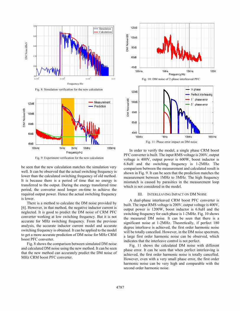
Fig. 8 shows the comparison between simulated DM noise
and calculated DM noise using the new method. It can be seen
that the new method can accurately predict the DM noise of
MHz CRM boost PFC converter.
In order to verify the model, a single phase CRM boost
PFC converter is built. The input RMS voltage is 200V, output
voltage is 400V, output power is 600W, boost inductor is
6.8uH and the switching frequency is 1-2MHz. The
comparison between the measurement and calculated result is
shown in Fig. 9. It can be seen that the prediction matches the
measurement between 1MHz to 3MHz. The high frequency
mismatch is caused by parasitics in the measurement loop
which is not considered in the model.
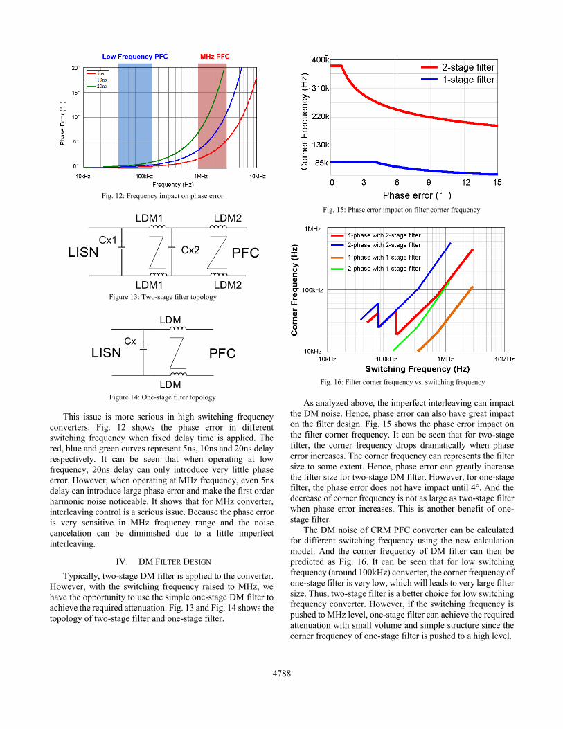
III. INTERLEAVING IMPACT ON DM NOISE
A dual-phase interleaved CRM boost PFC converter is
built. The input RMS voltage is 200V, output voltage is 400V,
output power is 1200W, boost inductor is 6.8uH and the
switching frequency for each phase is 1-2MHz. Fig. 10 shows
the measured DM noise. It can be seen that there is a
significant noise at 1-2MHz. Theoretically, if perfect 180
degree interleave is achieved, the first order harmonic noise
will be totally cancelled. However, in the DM noise spectrum,
a large first order harmonic noise can be observed, which
indicates that the interleave control is not perfect.
Fig. 11 shows the calculated DM noise with different
phase error. It can be seen that when perfect interleaving is
achieved, the first order harmonic noise is totally cancelled.
However, even with a very small phase error, the first order
harmonic noise can be very high and comparable with the
second order harmonic noise.
Fig. 8: Simulation verification for the new calculation
1 105
1 106
1 107
1 108
80
100
120
140
160
180
Simulation
Calculation
Frequency/Hz
DM
Nois
e/dB
uV
Fig. 9: Experiment verification for the new calculation
Fig. 10: DM noise of 2-phase interleaved PFC
Fig. 11: Phase error impact on DM noise
4787
This issue is more serious in high switching frequency
converters. Fig. 12 shows the phase error in different
switching frequency when fixed delay time is applied. The
red, blue and green curves represent 5ns, 10ns and 20ns delay
respectively. It can be seen that when operating at low
frequency, 20ns delay can only introduce very little phase
error. However, when operating at MHz frequency, even 5ns
delay can introduce large phase error and make the first order
harmonic noise noticeable. It shows that for MHz converter,
interleaving control is a serious issue. Because the phase error
is very sensitive in MHz frequency range and the noise
cancelation can be diminished due to a little imperfect
interleaving.
IV. DM FILTER DESIGN
Typically, two-stage DM filter is applied to the converter.
However, with the switching frequency raised to MHz, we
have the opportunity to use the simple one-stage DM filter to
achieve the required attenuation. Fig. 13 and Fig. 14 shows the
topology of two-stage filter and one-stage filter.
As analyzed above, the imperfect interleaving can impact
the DM noise. Hence, phase error can also have great impact
on the filter design. Fig. 15 shows the phase error impact on
the filter corner frequency. It can be seen that for two-stage
filter, the corner frequency drops dramatically when phase
error increases. The corner frequency can represents the filter
size to some extent. Hence, phase error can greatly increase
the filter size for two-stage DM filter. However, for one-stage
filter, the phase error does not have impact until 4°. And the
decrease of corner frequency is not as large as two-stage filter
when phase error increases. This is another benefit of one-
stage filter.
The DM noise of CRM PFC converter can be calculated
for different switching frequency using the new calculation
model. And the corner frequency of DM filter can then be
predicted as Fig. 16. It can be seen that for low switching
frequency (around 100kHz) converter, the corner frequency of
one-stage filter is very low, which will leads to very large filter
size. Thus, two-stage filter is a better choice for low switching
frequency converter. However, if the switching frequency is
pushed to MHz level, one-stage filter can achieve the required
attenuation with small volume and simple structure since the
corner frequency of one-stage filter is pushed to a high level.
Fig. 12: Frequency impact on phase error
Figure 13: Two-stage filter topology
Figure 14: One-stage filter topology
Fig. 15: Phase error impact on filter corner frequency
Fig. 16: Filter corner frequency vs. switching frequency
4788

It also can be seen from the figure that with two-phase
interleaved converter, the corner frequency of filter can be
greatly increased and the filter can be further reduced.
Therefore, one-stage DM filter is applied to the converter.
The filter topology is shown in Fig. 14. For the single phase
MHz PFC converter, it requires 61dB attenuation at 1MHz.
The corner frequency of DM filter can then be calculated as
31kHz, which matches the prediction results in Fig. 16. Cx is
closed to be 390nF, LDM is 91.2uH. The DM noise after filter
attenuation is shown in Fig. 17. The attenuated noise can meet
the standard.
Fig. 18 shows the DM filter size comparison for different
PFC converters. 50% volume reduction is achieved by
pushing switching frequency from 100kHz to 1MHz. Another
20% volume reduction is achieved by interleaving two-phase
PFC converter. Further volume reduction can be achieved if
perfect interleaving is guaranteed.
V. CONCLUSION
The major contribution of this paper is providing a more
accurate mathematical model to characterize the inductor
current for MHz CRM boost PFC converter. Based on this
model, the switching frequency variation can be predicted
accurately. Furthermore, the DM noise of MHZ CRM boost
PFC converter can be calculated and the results is verified by
both simulation and experiment. The DM noise EMI filter is
then designed. The filter corner frequency can be calculated
based on the model and it shows that high switching frequency
can help increase the corner frequency of filter and reduce
filter size. In addition, the interleaving impact on DM noise is
analyzed. For MHz PFC converter, very little time delay can
harm the interleaving performance and diminish the noise
cancelation effect.
REFERENCES
[1] Jih-Sheng Lai; Chen, D., "Design consideration for power factor correction boost converter operating at the boundary of continuous conduction mode and discontinuous conduction mode," Applied Power Electronics Conference and Exposition, 1993. APEC '93. Conference Proceedings 1993., Eighth Annual , vol., no., pp.267,273, 7-11 Mar 1993
[2] Sebastian, J.; Cobos, J.A.; Lopera, J.M.; Uceda, J., "The determination of the boundaries between continuous and discontinuous conduction modes in PWM DC-to-DC converters used as power factor preregulators," Power Electronics, IEEE Transactions on , vol.10, no.5, pp.574,582, Sep 1995
[3] Jindong Zhang; Shao, J.; Peng Xu; Lee, F.C.; Jovanovic, M.M., "Evaluation of input current in the critical mode boost PFC converter for distributed power systems," Applied Power Electronics Conference and Exposition, 2001. APEC 2001. Sixteenth Annual IEEE , vol.1, no., pp.130,136 vol.1, 2001
[4] Nussbaumer, T.; Heldwein, M.L.; Kolar, J.W., "Differential Mode Input Filter Design for a Three-Phase Buck-Type PWM Rectifier Based on Modeling of the EMC Test Receiver," Industrial Electronics, IEEE Transactions on , vol.53, no.5, pp.1649,1661, Oct. 2006
[5] Raggl, K.; Nussbaumer, T.; Kolar, J.W., "Guideline for a Simplified Differential-Mode EMI Filter Design," Industrial Electronics, IEEE Transactions on , vol.57, no.3, pp.1031,1040, March 2010
[6] Zijian Wang; Shuo Wang; Pengju Kong; Lee, F.C., "DM EMI Noise Prediction for Constant On-Time, Critical Mode Power Factor Correction Converters," Power Electronics, IEEE Transactions on , vol.27, no.7, pp.3150,3157, July 2012
Fig. 17: Filter attenuation result
(a)
(b)
(c)
Fig. 18: DM filter size comparison. (a) 100kHz PFC DM filter; (b)
1MHz single-phase PFC DM filter; (c) 1MHz two-phase PFC DM filter
4789
View publication statsView publication stats


![Bridgeless Buck-Boost PFC Converter for Multistring LED Driver€¦ · boost converter as a universal PFC converter [6]. In order to address these issues, a buck-boost converter is](https://img.pdfslide.us/doc/110x75/5eaabf2a4ab79d1e774f9005/bridgeless-buck-boost-pfc-converter-for-multistring-led-driver-boost-converter-as.jpg)