Embed Size (px)
Citation preview
Power Factor Correction for aBidirectional On-Board Charger forElectric Vehicles and Plug-in HybridElectric VehiclesA fundamental study of the bidirectional
totem-pole PFC
Sondre Westby Johannessen
Master of Energy and Environmental Engineering
Supervisor: Roy Nilsen, IELCo-supervisor: Tore Undeland, IEL
Torbjørn Sørsdahl, Valeo Siemens eAutomotive
Department of Electric Power Engineering
Submission date: June 2018
Norwegian University of Science and Technology

Abstract
With the beginning implementation of a ”smart grid” in industrialized countries in-creasing the load flexibility of customers, as well as communication with the gridoperators, a potential market for bidirectional on-board chargers (OBC) is emerg-ing. The OBC is the electric vehicle charger located within the vehicle, operatingas a link between the DC-voltage battery and the AC grid voltage in electricitysockets anywhere, thus working at a universal voltage range (85Vrms-265Vrms)with rated power in the range of 1.9kW to 3.5kW. To maximize the real powerdrawn by these OBCs, they are designed with power factor correction (PFC) con-verters at the AC grid interface, shaping the drawn AC current sinusoidally andin phase with the AC voltage, to maximize the power factor. Thus, a bidirec-tional OBC would necessarily require a bidirectional PFC. In this master’s thesis,a simulation model is developed for a bidirectional totem-pole PFC, attemptingto verify the use of this topology as the mentioned bidirectional OBC PFC. Thework is focused on describing the basic bidirectional operation of the bidirectionaltotem-pole PFC, deriving expressions for currents, voltages and losses, as well asfor the gate logic and control system. Average current mode control is used, withcascaded current and voltage control including PI controllers and Symmetrical op-timum tuning. To verify the simulation model for the power levels and demandsof an OBC, the main components are dimensioned to achieve 98% efficiency at230Vrms, 3.5kW and 90kHz switching frequency, implementing GaN eHEMTs inthe fast-switching leg of the totem-pole. At last, simulations are performed, show-ing that the PFC is able to achieve a power factor of 0.998 and a THD of 5% inboth G2V and V2G, without a DM filter on the AC side.

Sammendrag
Etter hvert som implementeringen av ”smarte nett” er i ferd med a skyte fart i in-dustrialiserte land, med økt lastfleksibilitet pa kundesiden og økt kommunikasjonmot nettoperatørene, begynner det a apne seg et marked for bidireksjonelle sakalte”on-board chargers” (OBC-er). En OBC er elbilladeren som er plasserte inne ielbilen og fungerer som en link mellom elbilbatteriet - som krever DC-spenning -og AC-spenningen i strømuttaket, hvilket betyr at den ma designes for a operereved universell AC-spenning (85Vrms-265Vrms) og nominelle effektnivaer mellom1.9kW og 3.5kW. For a maksimere den reelle effekten trukket av OBC-en, er dedesignet med sakalte ”power factor corretion”-omformere (PFC-er) pa AC-sidenut mot nettet. Denne kontrollerer AC-strømmen som trekkes til a være formet somen sinus og i fase med AC-spenningen pa nettet, for pa den maten a maksimereeffektfaktoren. Av den grunn, vil nødvendigvis en bidireksjonell OBC behøve enbidireksjonell PFC. I denne masteravhandlingen vil det bli utviklet en sakalt bidi-reksjonell ”totem-pole PFC”, mens det forsøkes a verifisere hvorvidt dennetopolo-gien egner seg for bruk i en bidireksjonell PFC for en OBC. Hovedfokus for opp-gaven vil ligge i a beskrive hvordan en bidireksjonell totem-pole PFC fungerergrunnleggende, mens det vil utledes uttrykk for strømmer, spenninger og tap i om-formeren, samt gate-logikken og kontrollsystemet. ”Average current mode” brukesi kontrollsystemet, med dobbel kontrollsløyfe med strøm- og spenningskontroll,begge to med PI-regulatorer dimensjonert med Symmetrisk optimum. For a ver-ifisere simuleringsmodellen for de aktuelle spennings- og effektnivaene, dimen-sjoneres de viktigste komponentene til a opna 98% virkningsgrad ved 230Vrms,3,5kW og 90kHz switchefrekvens, med GaN eHEMT-er implementert i det hurtig-switchende totem-pole-benet. Til slutt ble det utført simuleringer av modellen, ogdisse viser at den bidireksjonelle totem-pole PFC-en oppnar en effektfaktor pa0.998 og en THD pa 5% bade under G2V og V2G, uten filter pa AC-siden.

Preface
This master’s thesis is conducted during the spring 2018, and it is the finishingwork of a master’s degree in Energy and Environmental Engineering at the Nor-wegian University of Science and Technology (NTNU), Department of ElectricPower Engineering. The thesis focuses on power electronics, and it is a continua-tion of a specialization project performed during the autumn 2017, both of whichhave been announced and guided by Valeo Siemens eAutomotive.
I would like to thank my supervisor, Roy Nilsen, for his valuable guidance and sup-port through numerous guidance sessions throughout the year, and co-supervisor,Tore M. Undeland, for his expert advice. My sincere gratitude goes to TorbjørnSørsdahl at Valeo Siemens for his effort, advice and guidance throughout the year.Thanks also to the rest of the staff at Valeo Siemens in Drammen who were readyto answer any of my questions without hesitation, during my stays there throughthe year.
Finally, I would like to place a warm thanks to my family for their loving support,and to my favourite Ingunn for letting me know when it is time to go home for thenight.


Table of Contents
Abstract i
Sammendrag ii
Preface iii
Table of Contents viii
List of Tables ix
List of Figures xiii
Acronyms xiv
1 Introduction 11.1 Motivation . . . . . . . . . . . . . . . . . . . . . . . . . . . . . . 21.2 The Bidirectional On-Board Charger . . . . . . . . . . . . . . . . 41.3 The bidirectional PFC . . . . . . . . . . . . . . . . . . . . . . . . 71.4 Scope of work . . . . . . . . . . . . . . . . . . . . . . . . . . . . 10
2 Basic operation of the bidirectional totem-pole PFC 132.1 G2V operation . . . . . . . . . . . . . . . . . . . . . . . . . . . 142.2 V2G operation . . . . . . . . . . . . . . . . . . . . . . . . . . . 162.3 Boost inductor . . . . . . . . . . . . . . . . . . . . . . . . . . . . 18
2.3.1 Current waveforms and ripple . . . . . . . . . . . . . . . 18
v

2.3.2 Conduction losses . . . . . . . . . . . . . . . . . . . . . 202.4 Transistors . . . . . . . . . . . . . . . . . . . . . . . . . . . . . . 22
2.4.1 Current waveforms and ripple . . . . . . . . . . . . . . . 222.4.2 Conduction losses . . . . . . . . . . . . . . . . . . . . . 252.4.3 Switching losses . . . . . . . . . . . . . . . . . . . . . . 27
2.5 DC-link . . . . . . . . . . . . . . . . . . . . . . . . . . . . . . . 302.5.1 Current waveforms and ripple . . . . . . . . . . . . . . . 302.5.2 Conduction losses . . . . . . . . . . . . . . . . . . . . . 32
3 Components dimensioning 353.1 DC-link capacitor . . . . . . . . . . . . . . . . . . . . . . . . . . 36
3.1.1 DC-link rated voltage . . . . . . . . . . . . . . . . . . . . 363.1.2 DC-link rated current . . . . . . . . . . . . . . . . . . . . 383.1.3 DC-link capacitance value . . . . . . . . . . . . . . . . . 383.1.4 Capacitor choice . . . . . . . . . . . . . . . . . . . . . . 39
3.2 Transistors . . . . . . . . . . . . . . . . . . . . . . . . . . . . . . 413.2.1 Choice of transistor technology . . . . . . . . . . . . . . 413.2.2 Guesstimating component loss distribution . . . . . . . . 433.2.3 Totem-leg transistors . . . . . . . . . . . . . . . . . . . . 453.2.4 Switching frequency . . . . . . . . . . . . . . . . . . . . 473.2.5 Comparison to state-of-the-art MOSFETs . . . . . . . . . 483.2.6 Rectifier-leg transistors . . . . . . . . . . . . . . . . . . . 49
3.3 Boost inductor . . . . . . . . . . . . . . . . . . . . . . . . . . . . 513.3.1 Boost inductance value . . . . . . . . . . . . . . . . . . . 513.3.2 RMS current rating . . . . . . . . . . . . . . . . . . . . . 523.3.3 Saturation current rating . . . . . . . . . . . . . . . . . . 523.3.4 Choice of inductor . . . . . . . . . . . . . . . . . . . . . 53
4 Drive and control 554.1 Gate drive logic . . . . . . . . . . . . . . . . . . . . . . . . . . . 56
4.1.1 Rectifier leg . . . . . . . . . . . . . . . . . . . . . . . . . 564.1.2 Totem leg . . . . . . . . . . . . . . . . . . . . . . . . . . 584.1.3 Waveforms . . . . . . . . . . . . . . . . . . . . . . . . . 61
4.2 Control system . . . . . . . . . . . . . . . . . . . . . . . . . . . 634.2.1 Control logic . . . . . . . . . . . . . . . . . . . . . . . . 654.2.2 Current control loop . . . . . . . . . . . . . . . . . . . . 70
4.2.3 Voltage control loop . . . . . . . . . . . . . . . . . . . . 78
5 System-level simulations 85
6 Feasibility of the bidirectional totem-pole PFC 896.1 Model shortcomings . . . . . . . . . . . . . . . . . . . . . . . . 896.2 Loss comparison to a regular boost PFC . . . . . . . . . . . . . . 91
6.2.1 Comparison at worst-case operating temperature . . . . . 936.2.2 Comparison at normal operating conditions . . . . . . . . 946.2.3 Comparison at 120Vrms . . . . . . . . . . . . . . . . . . 95
7 Conclusion and Further Work 977.1 Conclusion . . . . . . . . . . . . . . . . . . . . . . . . . . . . . 977.2 Further Work . . . . . . . . . . . . . . . . . . . . . . . . . . . . 99
Bibliography 101
Appendices 109
A Valeo Siemens bidirectional OBC specifications 111
B Literature review on power factor correction converters 121B.1 Power factor correction AC-DC converter . . . . . . . . . . . . . 121
B.1.1 Conventional PFC . . . . . . . . . . . . . . . . . . . . . 122B.1.2 Bidirectional PFC . . . . . . . . . . . . . . . . . . . . . 124
C Paper on GaN HEMTs and bidirectional PFCs 129
D 137D.1 Modulus Optimum in current loop . . . . . . . . . . . . . . . . . 137
D.1.1 PI controller parameters . . . . . . . . . . . . . . . . . . 137D.1.2 Current measurement filter design with Modulus optimum 138D.1.3 Simulations . . . . . . . . . . . . . . . . . . . . . . . . . 139
E Implemented Simulink model 141
F MATLAB code 145F.1 Controller tuning script . . . . . . . . . . . . . . . . . . . . . . . 145

F.2 Filter graphical solver . . . . . . . . . . . . . . . . . . . . . . . . 149
G System-level simulations 153
List of Tables
1.1 Demands and specifications for the bidirectional universal OBC,from [1] . . . . . . . . . . . . . . . . . . . . . . . . . . . . . . . 11
1.2 PFC-specific demands and specifications . . . . . . . . . . . . . . 12
3.1 Key parameters for the relevant electrolytic capacitor used by Va-leo Siemens today. [1] . . . . . . . . . . . . . . . . . . . . . . . 39
3.2 Guesstimated design rule losses distribution in the bidirectionaltotem-pole PFC. . . . . . . . . . . . . . . . . . . . . . . . . . . . 45
3.3 Some key parameters and rated values of the GaN Systems eHEMTsat Tcase = 25C. . . . . . . . . . . . . . . . . . . . . . . . . . . . 46
3.4 Calculated conduction losses of the eHEMT models. . . . . . . . 473.5 Estimated switching energy, losses and frequency of GS66516. . . 473.6 Some key parameters and rated values of MOSFET IPW60R045CPA
at Tcase = 25C. . . . . . . . . . . . . . . . . . . . . . . . . . . . 503.7 Estimated inductor parameters based on technology used by Valeo
Siemens today.[1] . . . . . . . . . . . . . . . . . . . . . . . . . . 53
ix


List of Figures
1.1 A sketch of the current Valeo Siemens OBC topology [1] . . . . . 41.2 The basic bidirectional PFC topology . . . . . . . . . . . . . . . 8
2.1 The basic bidirectional totem-pole topology . . . . . . . . . . . . 132.2 The G2V operation of the bidirectional totem-pole PFC. . . . . . 152.3 The V2G operation of the bidirectional totem-pole PFC. . . . . . 172.4 CCM iL and vL ripple over one switching period . . . . . . . . . . 182.5 Boost CCM ∆iL vs duty cycle . . . . . . . . . . . . . . . . . . . . 192.6 The inductor current compared to the AC mains voltage through-
out one mains cycle. . . . . . . . . . . . . . . . . . . . . . . . . 202.7 The rectifier-leg transistor drain-source currents throughout one
mains cycle during G2V. . . . . . . . . . . . . . . . . . . . . . . 222.8 The current ripple of the totem-leg switches during positive mains
half cycle in G2V operation. . . . . . . . . . . . . . . . . . . . . 232.9 The totem-leg transistor drain-source currents throughout one mains
cycle during G2V. . . . . . . . . . . . . . . . . . . . . . . . . . . 252.10 Approximation of the switching characteristics of a MOSFET. . . 282.11 Illustration of he DC-link capacitor, voltage and currents . . . . . 302.12 The current through the DC-link capacitor over one totem-leg switch-
ing period . . . . . . . . . . . . . . . . . . . . . . . . . . . . . . 312.13 The DC-side currents throughout one mains cycle during G2V. . . 31
3.1 DC-link voltage design requirements compared to AC mains voltage. 37
xi
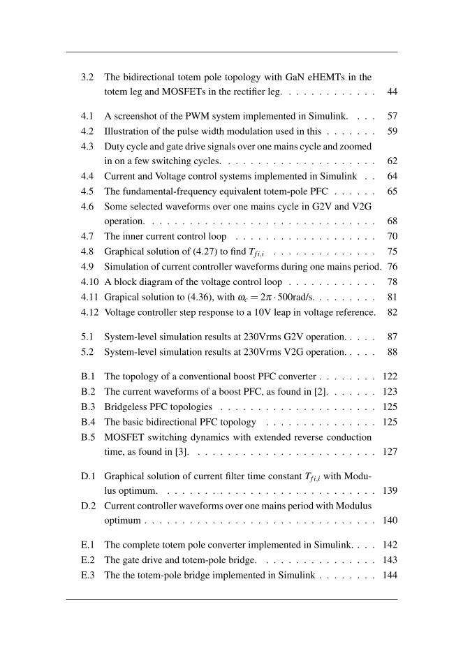
3.2 The bidirectional totem pole topology with GaN eHEMTs in thetotem leg and MOSFETs in the rectifier leg. . . . . . . . . . . . . 44
4.1 A screenshot of the PWM system implemented in Simulink. . . . 574.2 Illustration of the pulse width modulation used in this . . . . . . . 594.3 Duty cycle and gate drive signals over one mains cycle and zoomed
in on a few switching cycles. . . . . . . . . . . . . . . . . . . . . 624.4 Current and Voltage control systems implemented in Simulink . . 644.5 The fundamental-frequency equivalent totem-pole PFC . . . . . . 654.6 Some selected waveforms over one mains cycle in G2V and V2G
operation. . . . . . . . . . . . . . . . . . . . . . . . . . . . . . . 684.7 The inner current control loop . . . . . . . . . . . . . . . . . . . 704.8 Graphical solution of (4.27) to find Tf i,i . . . . . . . . . . . . . . 754.9 Simulation of current controller waveforms during one mains period. 764.10 A block diagram of the voltage control loop . . . . . . . . . . . . 784.11 Grapical solution to (4.36), with ωc = 2π ·500rad/s. . . . . . . . . 814.12 Voltage controller step response to a 10V leap in voltage reference. 82
5.1 System-level simulation results at 230Vrms G2V operation. . . . . 875.2 System-level simulation results at 230Vrms V2G operation. . . . . 88
B.1 The topology of a conventional boost PFC converter . . . . . . . . 122B.2 The current waveforms of a boost PFC, as found in [2]. . . . . . . 123B.3 Bridgeless PFC topologies . . . . . . . . . . . . . . . . . . . . . 125B.4 The basic bidirectional PFC topology . . . . . . . . . . . . . . . 125B.5 MOSFET switching dynamics with extended reverse conduction
time, as found in [3]. . . . . . . . . . . . . . . . . . . . . . . . . 127
D.1 Graphical solution of current filter time constant Tf i,i with Modu-lus optimum. . . . . . . . . . . . . . . . . . . . . . . . . . . . . 139
D.2 Current controller waveforms over one mains period with Modulusoptimum . . . . . . . . . . . . . . . . . . . . . . . . . . . . . . . 140
E.1 The complete totem pole converter implemented in Simulink. . . . 142E.2 The gate drive and totem-pole bridge. . . . . . . . . . . . . . . . 143E.3 The the totem-pole bridge implemented in Simulink . . . . . . . . 144

G.1 System-level simulation results at 120Vrms G2V operation. . . . . 154G.2 System-level simulation results at 120Vrms V2G operation. . . . . 155

Abbreviations
AC: Alternating CurrentCCM: Continuous Conduction ModeCrCM: Critical Conduction ModeDAB: Dual Active BridgeDC: Direct CurrentDCM: Discontinuous Conduction ModeDM: Direct ModeDSO: Distribution System OperatorEMI: Electromagnetic InterferenceESR: Equivalent Series ResistanceEV: Electric VehicleG2V: Grid-to-VehicleGaN: Gallium NitrideHEMT: High Electron Mobility TransistorMOSFET: Metal-Oxide-Semiconductor Field-Effect TransistorOBC: On-Board ChargerPCB: Printed Circuit BoardPHEV: Plug-in Hybrid Electric VehiclePLL: Phase-Locked LoopPWM: Pulse Width ModulationRMS: Root Mean SquareSHBM: Single H-Bridge ModulationSiC: Silicon CarbideTHD: Total Harmonic DistortionV2G: Vehicle-to-GridV2H: Vehicle-to-HomeZCS: Zero-Current SwitchingZVS: Zero-Voltage Switching

Chapter 1Introduction
This master’s thesis is a continuation of a specialization project work performedon the same topic.[4] For that reason, some of the work described in this thesis isbased on some of the work performed and described in the specialization projectreport. The following figures are retrieved from the specialization project report:
• Figure 1.1
• Figure 2.1
• Figure 2.2
• Figure 2.3
Furthermore, the following sections contain large portions of text reproductionfrom the abovementioned specialization project report:
• Section 1.1
• Section 1.2
• Section 2.1
• Section 2.2
1
1.1 Motivation
In the quest of securing a more sustainable and renewable electric energy supply inindustrialized countries, the implementation of a ”smart grid” is picking up pace.The smart grid concept incentivizes more distributed renewable electricity produc-tion and increased consumption flexibility for the customer.[5] This developmentis exemplified by the extensive roll-out of advanced electricity consumption mea-surement systems for all households in Norway and numerous countries in the Eu-ropean Union, as well as an increasing amount of distributed solar power built ine.g. Germany and California. [6, 7, 8, 9] The first tendency introduces a potentialfor substantial increase in communication and control at the consumer side of theelectric power grid. The second introduces a possible problem of over-productionat times of day with high solar irradiation, giving stability issues for the utilities[10]. Combined, these two imply both a possibility and a need for distributed en-ergy storage in the grid, connecting battery storage units at the consumer end toeven out the big hourly differences in power production.
One part of this distributed energy storage could be the main batteries of elec-tric vehicles (EVs) and plug-in hybrid electric vehicles (PHEVs) when these areconnected to the electricity supply at home or at work. The number of EVs andPHEVs on the roads is increasing, and with that comes a big battery capacity thatcould be utilized for purposes other than vehicle propulsion. One example of suchutilization is using EV batteries as electricity grid stabilizers through vehicle-to-grid (V2G) charging. At any time when a big load or generating unit is connectedto or disconnected from the grid, there is an immediate power imbalance whichcauses a change in grid frequency. [11, Chapter 9] To ensure that the frequencystays within the limits of stability, charging or discharging a fleet of cars connectedto the grid could cover some of this immediate power imbalance before the slowergenerators reacts after some seconds or minutes to completely cover the wholeimbalance. A potential issue for EVs and PHEVs when enabling bidirectionalcharging is that the number of cycles increases. Since the battery degrades withevery cycle, this would help degrade the battery faster.[12, 13] With this sort ofV2G solution, however, utilizing the EV batteries as grid stabilizers, the charg-ing and discharging would be high-power for a short period of time, meaning thebattery would not fully charge or discharge. Such solutions are being tested these
2
days, where EV owners are paid for having their batteries available for the utilityto draw or inject power whenever needed.[14, 15, 16] Furthermore, if one is tofully exploit the grid-conditioning potential of the bidirectional OBC, it could alsobe modified to be able to deliver and consume reactive power, serving as a reactivepower compensator. [17]
Another possibility is that the battery owners control the power flow themselves,e.g. to store energy when the electricity price is low, say, when the car is connectedto a power supply at work. Later in the evening the power could be sold back tothe grid at a higher price, earning money from the price difference. Otherwiseit could be supplied to the household when the electricity price is high, savingmoney. Moreover, a discussed concept is vehicle-to-home (V2H) charging, whichallows the car battery to serve as an emergency power source, supplying criticalloads during power outages.[18] Yet another possibility for exploiting the EV bat-tery energy, is using the battery to provide standard grid-voltage AC power withinthe car, supplying applications like PC chargers, refrigerators or TVs. Further-more, when campers today are in need of AC power for various devices, such aslighting, microwaves, small cooktops or again refrigerators, they use a DC-AC in-verter connected to a bank of regular 12V car batteries.[19] If an AC power supplyis made available also in the exterior of the EV, then this could replace the need forsuch solutions and even increase the available energy compared to the 12V batterybank.
3
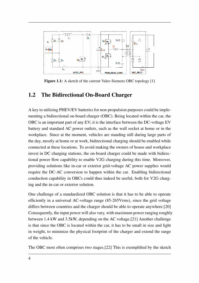
Figure 1.1: A sketch of the current Valeo Siemens OBC topology [1]
1.2 The Bidirectional On-Board Charger
A key to utilizing PHEV/EV batteries for non-propulsion purposes could be imple-menting a bidirectional on-board charger (OBC). Being located within the car, theOBC is an important part of any EV; it is the interface between the DC-voltage EVbattery and standard AC power outlets, such as the wall socket at home or in theworkplace. Since at the moment, vehicles are standing still during large parts ofthe day, mostly at home or at work, bidirectional charging should be enabled whileconnected at these locations. To avoid making the owners of house and workplaceinvest in DC charging stations, the on-board charger could be made with bidirec-tional power flow capability to enable V2G charging during this time. Moreover,providing solutions like in-car or exterior grid-voltage AC power supplies wouldrequire the DC-AC conversion to happen within the car. Enabling bidirectionalconduction capability in OBCs could thus indeed be useful, both for V2G charg-ing and the in-car or exterior solution.
One challenge of a standardized OBC solution is that it has to be able to operateefficiently in a universal AC-voltage range (85-265Vrms), since the grid voltagediffers between countries and the charger should be able to operate anywhere.[20]Consequently, the input power will also vary, with maximum power ranging roughlybetween 1.4 kW and 3.5kW, depending on the AC voltage.[21] Another challengeis that since the OBC is located within the car, it has to be small in size and lightin weight, to minimize the physical footprint of the charger and extend the rangeof the vehicle.
The OBC most often comprises two stages.[22] This is exemplified by the sketch
4
of the OBC topology used by Valeo Siemens eAutomotive (hereby referred to asValeo Siemens) reproduced in figure 1.1. Firstly, there is an AC-DC grid inter-face rectifier with power factor correction (PFC), sinusoidally shaping the drawnAC current in phase with the AC supply mains voltage, to maximize the powerfactor and remove low-order harmonics, while controlling the voltage ripple at theDC-link capacitor. The switching frequency of the PFC has to be kept high, in or-der to minimize the size of the inductor and the AC-side filter. At the same time, ahigher switching frequency causes higher switching losses, reducing the efficiency.Also, IEC 61000-4-6 defines limits to the emitted EMI in the frequency range of150kHz to 30MHz, so setting the switching frequency to exceed this lower limitwould mean that all of the harmonics needs to be filtered, increasing the size ofthe filter. Cascaded through the DC-link with this PFC is a DC-DC converter witha high-frequency transformer for galvanic isolation. The DC-DC is controllingthe battery-side voltage to be constant, for optimal performance. High switchingfrequency in the isolated DC-DC converter is decisive to minimize the weight andsize of inductors and the transformer, again decreasing the size and weight of thewhole OBC. However, in this case higher switching frequency does of course alsocause higher switching losses. The efficiency has to be kept high, defined by Va-leo Siemens to be above 94%, to maximize the charging speed.[1] The combinedmaximization of efficiency and power density (kW/dm3) is always going to be atrade-off, as explained in [23] with the Pareto front and exemplified with a boostPFC, where at a certain optimal limit, the increasing one is going to require a com-plementary decrease in the other. This is the compromise of an OBC, where thewish is both high efficiency and high power density. Price is also an importantfactor, as an OBC would be mass produced and should not lead to a big increasein vehicle cost.
Up until this point, the majority of commercial OBC solutions have been madeunidirectional, allowing only grid-to-vehicle (G2V) charging. To make the OBCcapable of bidirectional power flow and V2G, there can be no passive diode bridgerectifiers or standalone freewheeling diodes. Some diodes can be removed, imple-menting more compact solutions, while some have to be replaced by transistors,making the whole charger more complex in terms of control. Every transistorneeds its own drive circuit, meaning more transistors can also potentially requirea bigger charger volume. For that reason minimizing the number of transistors is
5

something that has to be considered when developing a bidirectional OBC.
With the smart grid still in its birth, the nature of bidirectional charging is stillnot clear, and different potential modes of operation present different demands forthe charger. If operated with the interior power outlet, using it for small TVs,refrigerators or laptop chargers, the charger would most likely be working at a lowload for a long period of time. On the other hand, if the vehicle is connected tothe grid, working in V2G operation, it could, as mentioned, either be used to sellthe battery power to the utility for a good price at times of high demand, or theDSO could use the charger capacity for grid stabilizing purposes. The first casecould give an even, high power transfer for hours at a time, while the latter wouldprovoke power transfers at maximum rated power for seconds or minutes. Thestress on components and operating efficiency would obviously be quite differentin these different cases, and it would be difficult to optimize the charger design forall modes of operation. For that reason, it will be assumed in this evaluation that thecharger will during V2G most often be under the control of the distribution systemoperator (DSO) to regulate stability. Therefore, the relevant PFC topologies willbe evaluated considering operation at maximum load for short periods of time.The basis of this decision is that this type of operation has already been testedand considered. The lower efficiency when supplying interior power supply isconsidered to be of less importance because the drawn power will be lower, andthus the stress and power dissipation will be small.
6
1.3 The bidirectional PFC
Having understood the basic composition of an OBC, it is clear that in order tomake a bidirectional OBC it is necessary with a bidirectional PFC. However, todesign a bidirectional PFC, it is also necessary to understand the basic operationof a unidirectional PFC. A literature review on unidirectional and bidirectionalPFCs was performed in the specialization project, and is attached in appendix B.This PFC introduction is based on that analysis. As stated there and above, thePFC is the grid interface of an OBC or another universal power supply, shapingthe drawn AC current sinusoidally and in phase with the AC voltage, and control-ling the internal DC-link voltage. The conventional boost PFC is structured as inthe OBC topology in figure 1.1, consisting of a passive rectifier cascaded with aregular boost converter.[24, ch. 7-4] Here, the switching of the boost transistor ismodulated to shape the fundamental inductor current according to the rectified ACvoltage seen from the rectifier.
The PFC operates either in continuous conduction mode (CCM), critical conduc-tion mode (CrCM) or discontinuous conduction mode (DCM), all of which are ex-plained in more detail and visualized in appendix B. CCM and CrCM are the mostcommonly used, where CCM has the advantage of lower current ripple, apply-ing less stress on the semiconductors and inductor and requiring a smaller direct-mode (DM) ac-side current filter, but at the same time yielding hard switching inboth turn-on and turn-off with corresponding higher switching losses. CrCM, onthe other hand, enables zero-current switching (ZCS) and possible zero-voltageswitching (ZVS) due to the current reaching zero every switching cycle, reducingswitching losses but at the same time generatng a large current ripple of twice theaverage current, increasing the stress on the components. For higher power ap-plications it is common to operate in CCM, because the stress on the componentswould otherwise get too high.[2]
An obvious disadvantage of the boost PFC with regard to bidirectional conduc-tion ability is the the presence of passive diodes both in the rectifier bridge andthe freewheeling diode, and so these need to be removed. A first step in that di-rection is including the operation of the transistor and freewheeling diode into therectifier bridge, making it a so-called bridgeless PFC, of which there are manyvariations.[25, 26] This integration has advantages with regards to losses, as the
7
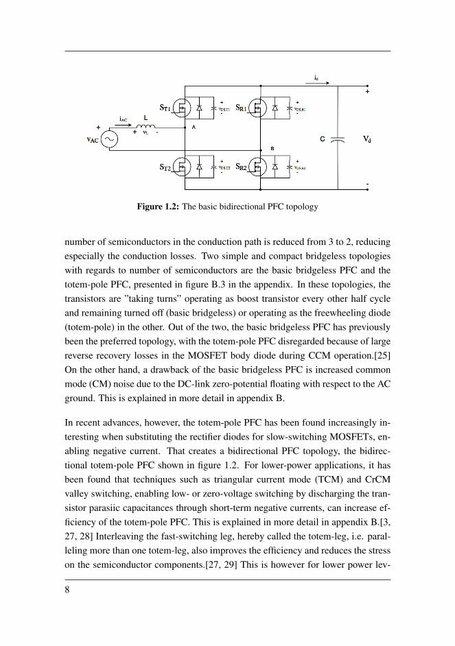
Figure 1.2: The basic bidirectional PFC topology
number of semiconductors in the conduction path is reduced from 3 to 2, reducingespecially the conduction losses. Two simple and compact bridgeless topologieswith regards to number of semiconductors are the basic bridgeless PFC and thetotem-pole PFC, presented in figure B.3 in the appendix. In these topologies, thetransistors are ”taking turns” operating as boost transistor every other half cycleand remaining turned off (basic bridgeless) or operating as the freewheeling diode(totem-pole) in the other. Out of the two, the basic bridgeless PFC has previouslybeen the preferred topology, with the totem-pole PFC disregarded because of largereverse recovery losses in the MOSFET body diode during CCM operation.[25]On the other hand, a drawback of the basic bridgeless PFC is increased commonmode (CM) noise due to the DC-link zero-potential floating with respect to the ACground. This is explained in more detail in appendix B.
In recent advances, however, the totem-pole PFC has been found increasingly in-teresting when substituting the rectifier diodes for slow-switching MOSFETs, en-abling negative current. That creates a bidirectional PFC topology, the bidirec-tional totem-pole PFC shown in figure 1.2. For lower-power applications, it hasbeen found that techniques such as triangular current mode (TCM) and CrCMvalley switching, enabling low- or zero-voltage switching by discharging the tran-sistor parasiic capacitances through short-term negative currents, can increase ef-ficiency of the totem-pole PFC. This is explained in more detail in appendix B.[3,27, 28] Interleaving the fast-switching leg, hereby called the totem-leg, i.e. paral-leling more than one totem-leg, also improves the efficiency and reduces the stresson the semiconductor components.[27, 29] This is however for lower power lev-
8
els; at the high power levels of an OBC (3.5kWmax) it is still desirable with CCMoperation, to have component stress at a satisfying level. Moreover, given the sizerestriction of an OBC and that the DM filter does in fact make up one third of theOBC volume, it is beneficial that the lower current ripple in CCM implies a smallerDM filter size.[1]
Beneficially, the most recent advances in wide-bandgap power semiconductor de-vices show that the Gallium Nitride (GaN) High-Electron-Mobility Transistor(HEMT) has been shown to give improvements on the performance of totem-polePFCs, when used in the fast-switching totem-leg. A literature study has been per-formed on GaN HEMTs and their application in bidirectional PFCs, and the resultsare presented in the paper attached in appendix C. The most notable advantage forapplication in the totem-pole PFC is that, unlike the MOSFET, the GaN HEMTdoes not contain a reverse body diode, thus solving the problem of reverse re-covery losses during CCM operation. Moreover, the GaN HEMTs show superiorconduction and switching characteristics all over, due to the combination of highbreakdown field and the low-resistivity 2DEG layer. This is explained in more de-tail in appendix C. In [30] is presented a 1.5kW, 65kHz CCM-operated totem-polePFC, showcasing an efficiency of 99%. Moreover, it is found through the litera-ture study that currently most 1-phase bidirectional two-stage OBCs proposed inthe scientific literature are using the bidirectional totem-pole PFC shown in figure2.1 [31, 32, 33]. In fact, most proposed 1-phase bidirectional PFCs overall areusing the bidirectional totem-pole topology [34, 35]. This indicates that it is possi-ble to design an efficient 3.5kW CCM-operated bidirectional totem-pole PFC. Forthat reason, the bidirectional totem-pole PFC will be the topology of choice goingforward in this master’s thesis.
9

1.4 Scope of work
Although a few cases of the bidirectional totem-pole PFC has appeared in the sci-entific literature, as presented in the previous section, the author has not comeacross any verification of the nature its fundamental bidirectional operation. Forthat reason, the main objective of this master’s thesis is to fill that hole, by deriv-ing and developing a fundamental simulation model describing the bidirectionaltotem-pole PFC and its bidirectional operation. This simulation model will be im-plemented in Simulink. To verify the use of the bidirectional totem-pole PFC ina bidirectional OBC, the simulation model will be implemented with off-the-shelfcomponents and a control system meeting some demands of a bidirectional OBCand PFC, shown in tables 1.1 and 1.2. The thesis is written in cooperation with Va-leo Siemens eAutomotive and is intended to be a building block for further workon a bidirectional OBC, verifying or dismissing the bidirectional totem-pole PFCas a technology to take further. In that sense, describing the currents, voltages andlosses in the basic operation of the topology will be important.
The topology will be investigated using MOSFETs and GaN HEMTs as the transis-tors, disregarding possible solutions with IGBTs. Furthermore, the PFC efficiencywill be optimized for a standard AC voltage of 230Vrms, not designing from theefficiency at 120Vrms. The design will be aiming to approach the current ValeoSiemens PFC designs with regards to switching frequency and efficiency, to usesimilar components and compare performance. As for the control system and gatelogic design, an emphasis will be put on making a solution which can be adapted toexisting unidirectional boost PFC control systems and gate drives, to create a flex-ible solution. For the PFC control average current mode control, whith cascadedcurrent and voltage loops containing PI controllers with Symmetrical optimumtuning.
In chapter 2, the basic operation of the bidirectional totem-pole PFC is described,deriving expressions for the currents and losses in the boost inductor, DC-linkcapacitor and transistors.
Chapter 3 will cover the design and dimensioning of the components, in particularthe boost inductor, transistors and DC-link capacitor.
In chapter 4 the bidirectional totem-pole control will be developed, deriving the
10
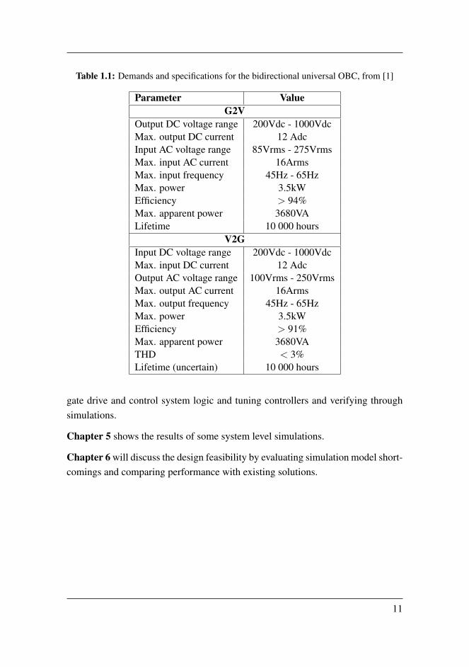
Table 1.1: Demands and specifications for the bidirectional universal OBC, from [1]
Parameter ValueG2V
Output DC voltage range 200Vdc - 1000VdcMax. output DC current 12 AdcInput AC voltage range 85Vrms - 275VrmsMax. input AC current 16ArmsMax. input frequency 45Hz - 65HzMax. power 3.5kWEfficiency > 94%Max. apparent power 3680VALifetime 10 000 hours
V2GInput DC voltage range 200Vdc - 1000VdcMax. input DC current 12 AdcOutput AC voltage range 100Vrms - 250VrmsMax. output AC current 16ArmsMax. output frequency 45Hz - 65HzMax. power 3.5kWEfficiency > 91%Max. apparent power 3680VATHD < 3%Lifetime (uncertain) 10 000 hours
gate drive and control system logic and tuning controllers and verifying throughsimulations.
Chapter 5 shows the results of some system level simulations.
Chapter 6 will discuss the design feasibility by evaluating simulation model short-comings and comparing performance with existing solutions.
11

Table 1.2: PFC-specific demands and specifications
Parameter ValueEfficiency G2V >98%Efficiency V2G >97%Min. DC-link voltage 340VMax. DC-link voltage ripple 20VMax. inductor current ripple 20%
12
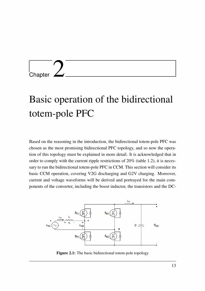
Chapter 2Basic operation of the bidirectionaltotem-pole PFC
Based on the reasoning in the introduction, the bidirectional totem-pole PFC waschosen as the most promising bidirectional PFC topology, and so now the opera-tion of this topology must be explained in more detail. It is acknowledged that inorder to comply with the current ripple restrictions of 20% (table 1.2), it is neces-sary to run the bidirectional totem-pole PFC in CCM. This section will consider itsbasic CCM operation, covering V2G discharging and G2V charging. Moreover,current and voltage waveforms will be derived and portrayed for the main com-ponents of the converter, including the boost inductor, the transistors and the DC-
Figure 2.1: The basic bidirectional totem-pole topology
13
link capacitor. Expressions will be developed for RMS currents and conductionand switching losses for these components. The relevant bidirectional totem-poletopology is shown in figure 2.1, and in the following all variables and parameterswill be referred to the notation in this figure.
2.1 G2V operation
In G2V operation, with power flow from AC source to DC link, the totem poleis operated as a boost converter with PWM switching, to shape the fundamentalwaveform of the AC current iAC like a sine in phase with the AC voltage vAC. [24]The operation is sketched in figure 2.2. During the positive mains half cycle, thelower totem-leg switch, ST 2 is operated with boost PWM switching (figure 2.2a),while the upper totem-leg switch ST 1 is operated complementarily; when ST 1 ison ST 2 is off, and vice versa. SR2 is always on during the positive half cycle.During the negative mains voltage half cycle, ST 1 is operated as a boost, ST 2 iscomplementary and SR1 is conducting. The AC current is governed by (2.1), andfrom that controlled by the average vAB, which is again controlled by the time-varying duty cycle, to be shaped like in figure B.2.
vL = vAC− vAB = LdiAC
dt(2.1)
14
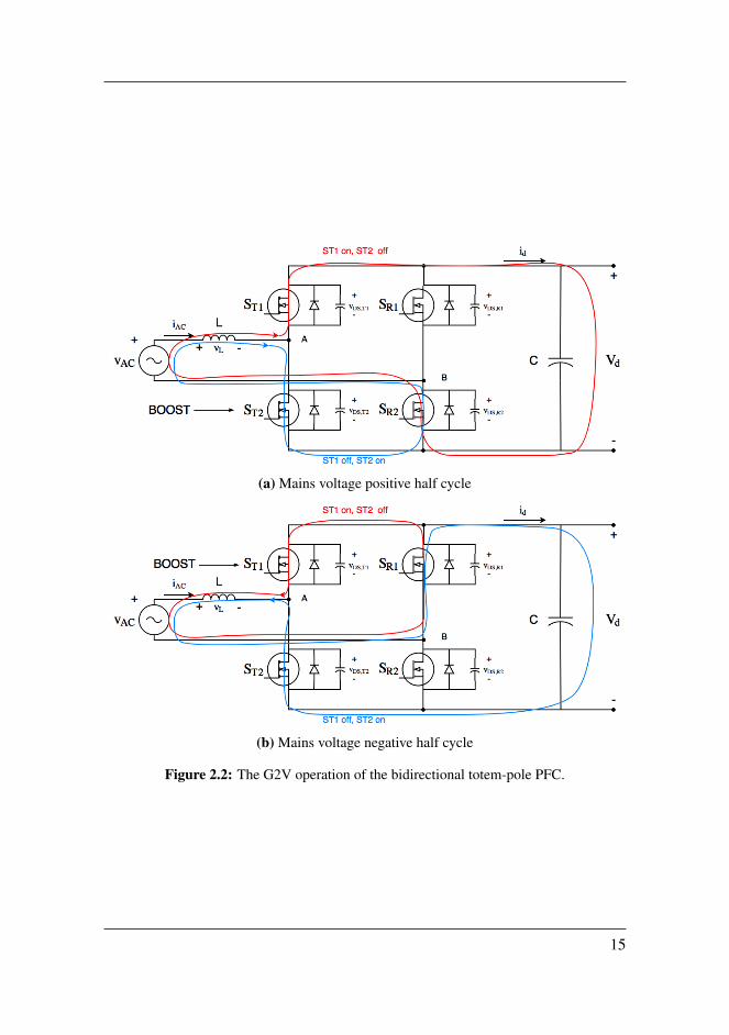
(a) Mains voltage positive half cycle
(b) Mains voltage negative half cycle
Figure 2.2: The G2V operation of the bidirectional totem-pole PFC.
15
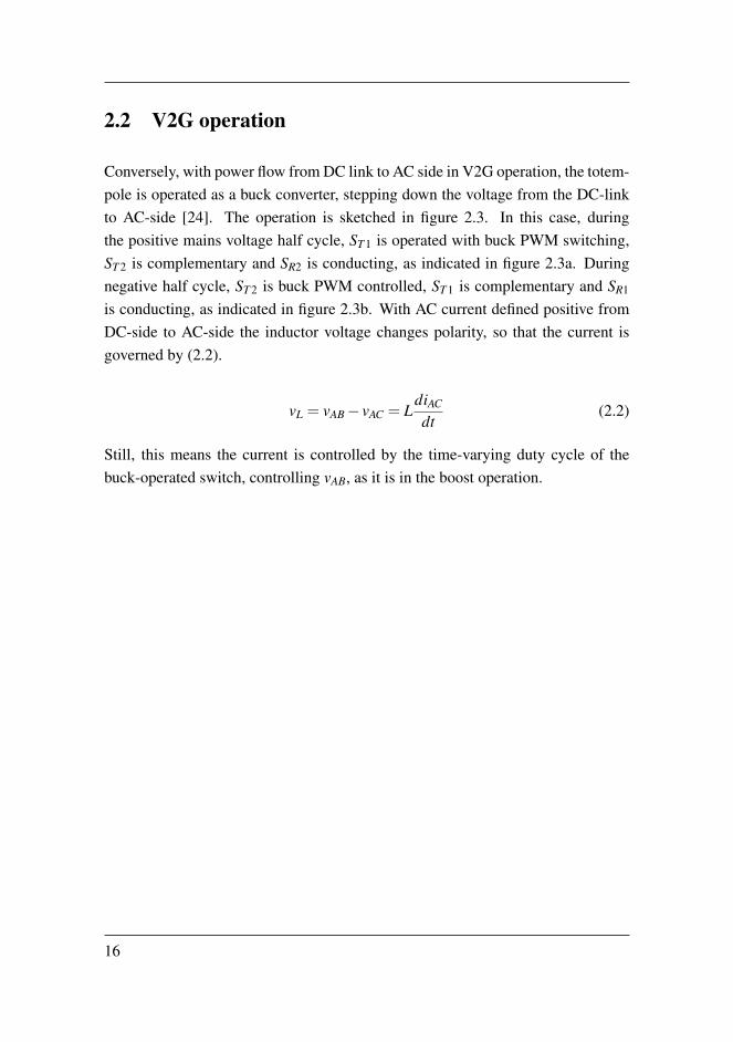
2.2 V2G operation
Conversely, with power flow from DC link to AC side in V2G operation, the totem-pole is operated as a buck converter, stepping down the voltage from the DC-linkto AC-side [24]. The operation is sketched in figure 2.3. In this case, duringthe positive mains voltage half cycle, ST 1 is operated with buck PWM switching,ST 2 is complementary and SR2 is conducting, as indicated in figure 2.3a. Duringnegative half cycle, ST 2 is buck PWM controlled, ST 1 is complementary and SR1
is conducting, as indicated in figure 2.3b. With AC current defined positive fromDC-side to AC-side the inductor voltage changes polarity, so that the current isgoverned by (2.2).
vL = vAB− vAC = LdiAC
dt(2.2)
Still, this means the current is controlled by the time-varying duty cycle of thebuck-operated switch, controlling vAB, as it is in the boost operation.
16
(a) Mains voltage positive half cycle
(b) Mains voltage negative half cycle
Figure 2.3: The V2G operation of the bidirectional totem-pole PFC.
17
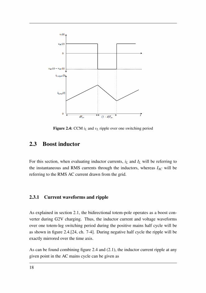
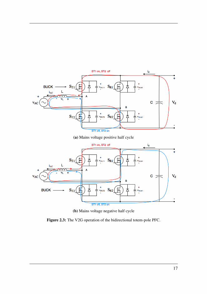
Figure 2.4: CCM iL and vL ripple over one switching period
2.3 Boost inductor
For this section, when evaluating inductor currents, iL and IL will be referring tothe instantaneous and RMS currents through the inductors, whereas IAC will bereferring to the RMS AC current drawn from the grid.
2.3.1 Current waveforms and ripple
As explained in section 2.1, the bidirectional totem-pole operates as a boost con-verter during G2V charging. Thus, the inductor current and voltage waveformsover one totem-leg switching period during the positive mains half cycle will beas shown in figure 2.4.[24, ch. 7-4]. During negative half cycle the ripple will beexactly mirrored over the time axis.
As can be found combining figure 2.4 and (2.1), the inductor current ripple at anygiven point in the AC mains cycle can be given as
18

Figure 2.5: Boost CCM ∆iL vs duty cycle
∆iL(t) =1L
∫ d·Tsw
t=0vAC(t)dt , (2.3)
where d is the duty cycle at this point. Since fsw fAC, vAC(t) and can be consid-ered constant over one switching period, giving from (2.3):
∆iL(t) =Tsw
Ld(t)vAC(t) (2.4)
Finally using the boost converter voltage ratio from [24, ch. 7-4],
vDC(t)vAC(t)
=1
1−d(t), (2.5)
(2.4) can be rewritten as follows:
∆iL(t) =TswvDC(t)
Ld(t)
(1−d(t)
). (2.6)
This equation (2.6) is solved graphically in figure 2.5, assuming vDC(t) is approx-imately constant and equal to vDC(t) ≈ VDC. Figure 2.5 shows that ∆iL(d) has aparabolic shape, peaking at d = 0.5.
For illustration, the current through the inductor, iAC, during G2V over a wholemains cycle is shown in figure 2.6. The average inductor current and the AC mainsvoltage are shown as well for comparison, and they show that the fundamental ACcurrent is more or less in phase with the AC voltage.
19
Figure 2.6: The inductor current compared to the AC mains voltage throughout one mainscycle.
2.3.2 Conduction losses
The inductor conduction losses mainly comprises two parts: copper losses, whichare resistive losses from the resistance in the inductor windings, and core losses,who are mostly due to eddy current losses end hystheresis losses in the magneticcore.[24, ch. 30-1] The hysteresis losses are highly dependent on the core material,but is always given on the following form:
PL,hyst = k · f a ·BqAC , (2.7)
where k, a and q are material dependent constants, f is the magnetic flux oscillationfrequency and BAC is the AC magnetic flux density.[24, ch. 30-1-2] Eddy currentlosses are also core dependent, given on the form:
PL,eddy =q2ω2(BAC +Bavg)
2
24ρcore, (2.8)
where ω is the angular frequency of the flux oscillations, Bavg is the flux densityconstant flux offset and ρcore is the charge density of the core material.[24, ch.30-1-4] As mentioned, the copper losses are resistive losses due to the windingresistance, and so they are given by:
20

PL,copper = RL,copperI2L , (2.9)
where IL is the RMS inductor current and RL,copper is the inductor winding resis-tance. Acknowledging that the core flux density B ∝ I by Ampere’s law, as well asthat q often takes a value close to 2,[24, ch. 30-1-2] it can be seen from (2.7), (2.8)and (2.9) that all of these losses have a nearly proportional relation to to I2
L . Thus,a simplification will be made going forward, merging all of these losses into oneequivalent resistance at the given frequency, called RL, giving the following lossequation:
PL ≈ RLI2L . (2.10)
As mentioned, the inductor current ripple must be less than 20%, and for thatreason it is assumed that
IL ≈ IAC , (2.11)
meaning (2.9) can be rewritten:
PL ≈ RLI2AC . (2.12)
21
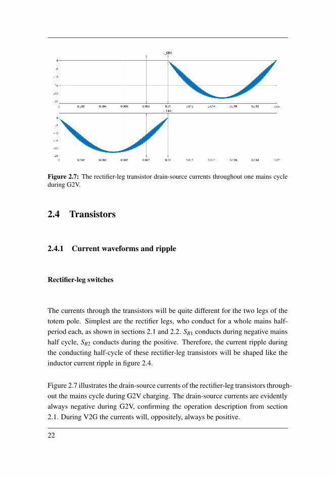
Figure 2.7: The rectifier-leg transistor drain-source currents throughout one mains cycleduring G2V.
2.4 Transistors
2.4.1 Current waveforms and ripple
Rectifier-leg switches
The currents through the transistors will be quite different for the two legs of thetotem pole. Simplest are the rectifier legs, who conduct for a whole mains half-period each, as shown in sections 2.1 and 2.2. SR1 conducts during negative mainshalf cycle, SR2 conducts during the positive. Therefore, the current ripple duringthe conducting half-cycle of these rectifier-leg transistors will be shaped like theinductor current ripple in figure 2.4.
Figure 2.7 illustrates the drain-source currents of the rectifier-leg transistors through-out the mains cycle during G2V charging. The drain-source currents are evidentlyalways negative during G2V, confirming the operation description from section2.1. During V2G the currents will, oppositely, always be positive.
22

(a) The current through the boost switch at an arbitrary point in the ACmains cycle.
(b) The totem-pole output current to the DC link at an arbitrary point inthe AC mains cycle.
Figure 2.8: The current ripple of the totem-leg switches during positive mains half cyclein G2V operation.
23
Totem-leg switches
The current of the two totem-pole transistors depend highly on the duty cycle dof each of the switches, since the transistors obviously only conducts while theyare on. The modulation is different for the different transistors in each mains half-cycle, as mentioned in sections 2.1 and 2.2, and so the switching-period currentwaveform of each of the transistors will be different as well. To simplify the anal-ysis, switching-period current waveforms will here be shown for the boost switchand the boost complementary switch during G2V. During V2G, the boost comple-mentary switch which will be equivalent to the buck switch, with the same currentwaveform, and the boost switch will be equivalent to the buck complementaryswitch.
Deriving the switching-period current waveforms from figure 2.4, the boost switchconducts during dTsw, whereas the boost complementary switch conducts during(1− d)Tsw. Hence, the switching-period current waveforms through the boostswitch and the boost complementary switch for an arbitrary duty cycle d can begiven as in figures 2.8a and 2.8b, respectively. The current through the boost com-plementary switch is the current that is passed from the totem-pole to the DC-link,and is therefore denoted iDC(t).
Throughout one mains cycle in G2V operation, the currents of the two switcheswill be shaped as in figure 2.9. As explained in section 2.1, ST 2 is the boost switchduring positive half-cycle, having the switching-period current waveform drawnin figure 2.8a, whereas during negative half-cycle it is the complementary switch,having the switching-period current waveform drawn in figure 2.8b, with negativepolarity. ST 1 is exactly opposite. During V2G, the currents have the same shape,but with opposite polarity.
24
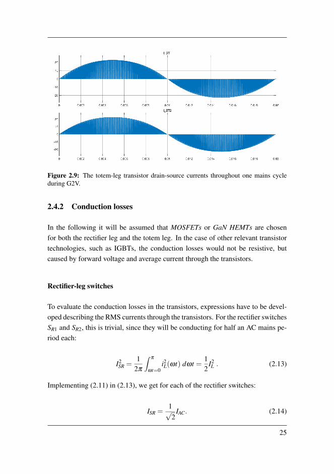
Figure 2.9: The totem-leg transistor drain-source currents throughout one mains cycleduring G2V.
2.4.2 Conduction losses
In the following it will be assumed that MOSFETs or GaN HEMTs are chosenfor both the rectifier leg and the totem leg. In the case of other relevant transistortechnologies, such as IGBTs, the conduction losses would not be resistive, butcaused by forward voltage and average current through the transistors.
Rectifier-leg switches
To evaluate the conduction losses in the transistors, expressions have to be devel-oped describing the RMS currents through the transistors. For the rectifier switchesSR1 and SR2, this is trivial, since they will be conducting for half an AC mains pe-riod each:
I2SR =
12π
∫π
ωt=0i2L(ωt) dωt =
12
I2L . (2.13)
Implementing (2.11) in (2.13), we get for each of the rectifier switches:
ISR =1√2
IAC. (2.14)
25
Totem-leg switches
In the case of the fast-switching totem-leg switches, ST 1 and ST 2, the RMS currentthrough each of the transistors depends on the time-varying duty cycle dST of therelevant transistor. The discrete-form equation for the RMS current through one ofthe totem-leg switches can be given as follows:
I2ST =
12π
fsw/ fAC
∑k=0
dST [k]i2L[k] , (2.15)
where k represents one single switching period at one point in the AC mains cycle,fsw is the switching frequency, fAC is the AC mains frequency and d in this caseis the duty cycle of any of the two totem-leg switches. Taking into account thatfsw will be chosen so that fsw fAC, (2.15) can be approximated as a continuousintegral over the whole AC mains cycle:
I2ST =
12π
∫ 2π
ωt=0d(ωt)i2L(ωt) dωt . (2.16)
Moreover, since ST 1 and ST 2 are switched complementarily, (2.16) can be sim-plified. Dead time required between turn-off of one transistor and turn-on of theother to avoid cross-conduction is neglected, since it is assumed very small.[24]The complementary switching means one of the switches are always conducting,and as explained in sections 2.1 and 2.2, the roles of the two switches interchangeevery half cycle. Thus, based on the current waveforms for the boost and comple-mentary switch in figures 2.8a and 2.8b, (2.16) can be rewritten as follows:
I2ST =
12π
(∫π
ωt=0d(ωt)i2L(ωt) dωt +
∫π
ωt=0
(1−d(ωt)
)i2L(ωt) dωt
)(2.17)
=1
2π
∫π
ωt=0
(d(ωt)+1−d(ωt)
)i2L(ωt) dωt (2.18)
=1
2π
∫π
ωt=0i2L(ωt) dωt (2.19)
=12
I2L (2.20)
26
This derivation from (2.17) to (2.20) shows that due to the symmetry of the topol-ogy, both of the totem-leg switches are conducting in total in half of the AC-mainsvoltage cycle. This gives the same RMS current in both of the totem-leg switchesas in the rectifier-leg switches:
IST =1√2
IAC . (2.21)
Based on the derived RMS current expressions in (2.14) and (2.21), the conductionlosses in each of the transistors can be determined as follows:
Pcond =12
I2ACRDS,on. (2.22)
2.4.3 Switching losses
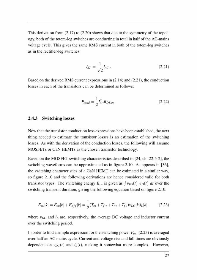
Now that the transistor conduction loss expressions have been established, the nextthing needed to estimate the transistor losses is an estimation of the switchinglosses. As with the derivation of the conduction losses, the following will assumeMOSFETs or GaN HEMTs as the chosen transistor technology.
Based on the MOSFET switching characteristics described in [24, ch. 22-5-2], theswitching waveforms can be approximated as in figure 2.10. As appears in [36],the switching characteristics of a GaN HEMT can be estimated in a similar way,so figure 2.10 and the following derivations are hence considered valid for bothtransistor types. The switching energy Esw is given as
∫vDS(t) · iD(t) dt over the
switching transient duration, giving the following equation based on figure 2.10:
Esw[k] = Eon[k]+Eo f f [k] =12(Tr,i +Tf ,v +Tr,v +Tf ,i)vDC[k]iL[k], (2.23)
where vDC and iL are, respectively, the average DC voltage and inductor currentover the switching period.
In order to find a simple expression for the switching power Psw, (2.23) is averagedover half an AC mains cycle. Current and voltage rise and fall times are obviouslydependent on vDC(t) and iL(t), making it somewhat more complex. However,
27
(a) Turn-on
(b) Turn-off
Figure 2.10: Approximation of the switching characteristics of a MOSFET.
28

vDC(t) will have a ripple of less than 20%,(table 1.2) meaning it can be assumed tobe approximately constant and equal to VDC, again giving approximately constantTr,v and Tfv . Since we are mostly interested in a rough estimate of the losses fortransistor dimensioning purposes, it is assumed for simplicity going forward thatalso the current rise and fall times do not vary much with time. To clean up theexpression, we set total switching commutation time Tsw,comm = Tr,i +Tf ,v +Tr,v +
Tf ,i. An expression for the average switching energy is obtained:
Esw,avg =1π
∫π
ωt=0Esw(ωt)dωt =
12
Tsw,commVDCIAC,avg , (2.24)
where the average AC current over one half period, IAC,avg, is given as
IAC,avg =1π
∫π
ωt=0iAC,avg(ωt)dωt =
2√
2π
IAC . (2.25)
This gives approximate transistor switching power loss:
Psw = fsw ∗Esw,avg =fsw
2Tsw,commVDCIAC,avg . (2.26)
29
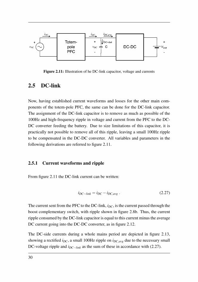
Figure 2.11: Illustration of he DC-link capacitor, voltage and currents
2.5 DC-link
Now, having established current waveforms and losses for the other main com-ponents of the totem-pole PFC, the same can be done for the DC-link capacitor.The assignment of the DC-link capacitor is to remove as much as possible of the100Hz and high-frequency ripple in voltage and current from the PFC to the DC-DC converter feeding the battery. Due to size limitations of this capacitor, it ispractically not possible to remove all of this ripple, leaving a small 100Hz rippleto be compensated in the DC-DC converter. All variables and parameters in thefollowing derivations are referred to figure 2.11.
2.5.1 Current waveforms and ripple
From figure 2.11 the DC-link current can be written:
iDC−link = iDC− iDC,avg . (2.27)
The current sent from the PFC to the DC-link, iDC, is the current passed through theboost complementary switch, with ripple shown in figure 2.8b. Thus, the currentripple consumed by the DC-link capacitor is equal to this current minus the averageDC current going into the DC-DC converter, as in figure 2.12.
The DC-side currents during a whole mains period are depicted in figure 2.13,showing a rectified iDC, a small 100Hz ripple on iDC,avg due to the necessary smallDC-voltage ripple and iDC−link as the sum of these in accordance with (2.27).
30
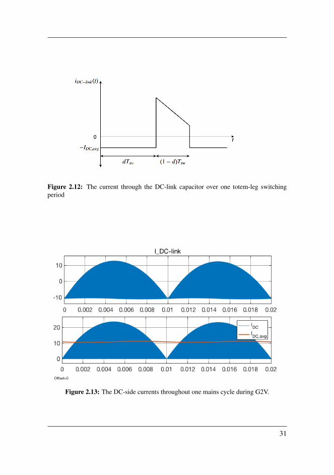
Figure 2.12: The current through the DC-link capacitor over one totem-leg switchingperiod
Figure 2.13: The DC-side currents throughout one mains cycle during G2V.
31

2.5.2 Conduction losses
Like in the other main components of the totem-pole PFC, there are some lossesin the DC-link capacitor which need to be taken into account in the PFC design.These are mostly dielectric losses and electrode losses, often simplified as conduc-tion losses due to an internal equivalent series resistance (ESR) of the capacitor.[37] A loss expression can be given as
PDC−link = I2DC−link ·ESR , (2.28)
where IDC−link is the RMS current through the DC-link capacitor. With IDC,avg
assumed constant, the DC-link current iDC−link consists of all of the harmonics iniDC. As explained in [24, ch. 3-2-4-1], using superposition of harmonic signals,the DC-link RMS current can again be given as follows:
IDC−link =√
I2DC,rms− I2
DC,avg , (2.29)
where IDC,rms is the RMS-value of the current from the totem pole to the DC-sideand IDC,avg is both the RMS and the constant value of the current to the DC-DCconverter. Since iDC is always the current through the complementary boost switch,and exploiting that iDC is symmetric every half period, the RMS current IDC can begiven from (2.13) over one half period:
I2DC =
1π
∫π
ωt=0dcompl(ωt)i2AC(ωt) dωt , (2.30)
where dcompl is the duty cycle of the complementary switch. It will be shown laterin section 4.2.1 that the duty cycle dcompl(ωt) ∝ vAB,1(ωt) = VAB sin(ωt + φAB)
from figure 2.1. Hence, (2.30) can be rewritten
I2DC =
1π
∫π
ωt=0dcompl sin(ωt +φAB)
(IAC sin(ωt)
)2 dωt , (2.31)
where φAB is the phase angle of vAB(ωt) referred to vAC(ωt). The peak duty dcompl
will be, using the basic boost converter properties from [24, ch. 7-4] and that the
32

duty cycle of the complementary switch is given as dcompl = 1−dboost :
dcompl = 1−dboost,min =VAC
VDC. (2.32)
Implementing (2.32) in (2.31) and solving, the DC RMS current becomes
I2DC,rms =
83π
VAC
VDCI2AC cos(φAB) . (2.33)
Implementing (2.33) in (2.29), the RMS current in the DC-link is given as follows:
IDC−link =
√8
3π
VAC
VDCI2AC cos(φAB)− I2
DC,avg , (2.34)
which easily gives the conduction losses when implementing in (2.28):
PDC−link =
(8
3π
VAC
VDCI2AC cos(φAB)− I2
DC,avg
)·ESR . (2.35)
33

34
Chapter 3Components dimensioning
Dimensioning the components is obviously important for building a physical em-bodiment of the PFC, but it is important for building the basic simulation modelas well. Various parameters in the PFC will affect the currents and voltages atdifferent points in the topology; e.g. loss considerations in boost inductor andtransistors dictating the average DC-link voltage, DC-link capacitor dictating theDC-link voltage ripple and the boost inductor – along with the DC-link voltage– dictating the AC current ripple. This chapter will revolve around dimensioningthe key components of the totem-pole PFC: The boost inductor, the transistors andthe DC-link capacitor. The components will be dimensioned assuming maximumpower flow both in G2V and V2G mode. This is justified by the following: DuringG2V, the consumer should be able to charge its car at maximum power when re-quired, and, during V2G, the OBC is likely to operate as a grid stabilizer supplyingthe grid at maximum power, as argued in section 1.1. All parameters and variableswill be referred to figure 2.1.
35
3.1 DC-link capacitor
The DC-link capacitor plays an important role in an OBC, suppressing much ofthe DC-link voltage ripple to keep the voltage as constant as possible without ex-ceeding the DC-link capacitor size limitations. This DC-link voltage is controlledby the PFC, making the DC-link capacitor central in PFC design. The battery onthe DC-side of the OBC requires DC voltage. Thus, a big part of the DC voltage100Hz ripple must be suppressed in the DC link before DC-DC converter com-pensates the rest. The DC-DC converter is often less efficient at compensating bigvariations in input voltage and current, meaning it is beneficial keeping the ripplelow at its input.[1] Moreover, since the PFC is working in boost operation duringG2V charging and buck during V2G discharging, another key reason for minimiz-ing the ripple is ensuring that the instantaneous DC-link voltage is always higherthan the instantaneous AC voltage. Moreover, the DC-link capacitor is the mostlimiting component to the lifetime of the OBC, and so the current rating should bechosen as high as possible and the ESR as low as possible to minimize the wearand tear of the capacitor. [1]
3.1.1 DC-link rated voltage
Valeo Siemens define for this application that the peak-to-peak 100Hz voltage rip-ple at the DC-link should be held at 20V, as specified in table 1.2. Furthermore,it is critical for the boost operation in G2V and buck operation in V2G that theinstantaneous DC-link voltage is always higher than the instantaneous magnitudeof vAC(t), as shown in figure 3.1. To allow for some delay in the voltage control, acertain margin, Vmargin, needs to be added. This margin is for this converter set at
Vmargin ≥ 5V .
As a consequence, with the peak-to-peak ripple of 20V, the average DC-link volt-age has to be set at
VDC ≥ VAC +15V .
At AC voltages of 230Vrms (325Vpeak) and lower, complying with the above-mentioned restrictions is not an issue, due to the minimum limit for VDC set at 340
36
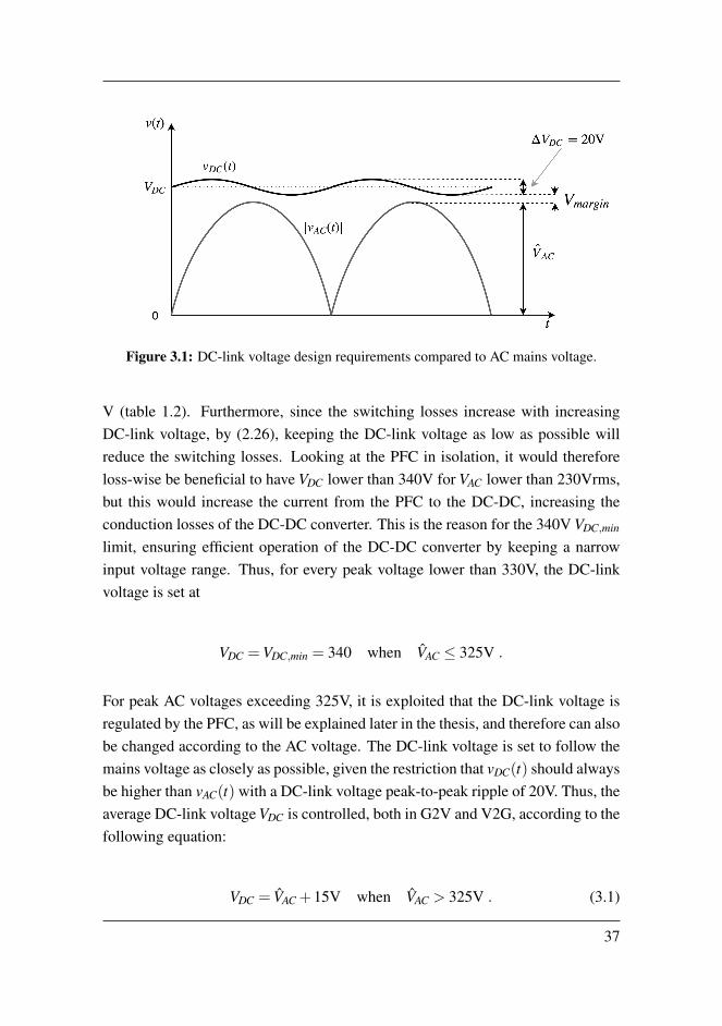
Figure 3.1: DC-link voltage design requirements compared to AC mains voltage.
V (table 1.2). Furthermore, since the switching losses increase with increasingDC-link voltage, by (2.26), keeping the DC-link voltage as low as possible willreduce the switching losses. Looking at the PFC in isolation, it would thereforeloss-wise be beneficial to have VDC lower than 340V for VAC lower than 230Vrms,but this would increase the current from the PFC to the DC-DC, increasing theconduction losses of the DC-DC converter. This is the reason for the 340V VDC,min
limit, ensuring efficient operation of the DC-DC converter by keeping a narrowinput voltage range. Thus, for every peak voltage lower than 330V, the DC-linkvoltage is set at
VDC =VDC,min = 340 when VAC ≤ 325V .
For peak AC voltages exceeding 325V, it is exploited that the DC-link voltage isregulated by the PFC, as will be explained later in the thesis, and therefore can alsobe changed according to the AC voltage. The DC-link voltage is set to follow themains voltage as closely as possible, given the restriction that vDC(t) should alwaysbe higher than vAC(t) with a DC-link voltage peak-to-peak ripple of 20V. Thus, theaverage DC-link voltage VDC is controlled, both in G2V and V2G, according to thefollowing equation:
VDC = VAC +15V when VAC > 325V . (3.1)
37

Based on this the maximum rated DC-link voltage in this design can be found tobe
VDC,max =√
2 ·275V+10V = 400V .
3.1.2 DC-link rated current
Finding the minimum DC-link current rating can be done easily using figures 2.12and 2.13 to recognize that the maximum DC-link current can be given as
IDC−link,max = IAC,max− IDC,avg,min , (3.2)
where IDC,avg,min is the minimum DC current at max power, which is given fromthe max power and minimum average DC-link voltage:
IDC,avg,min =3500W400V
= 8.75A ,
and the maximum DC-link current becomes, from (3.2):
IDC−link,max =√
2 ·16A−8.75A = 13.87A .
However, as mentioned earlier, the current rating should be chosen higher than thisto minimize the wear and tear of the DC-link capacitor.
3.1.3 DC-link capacitance value
The DC-link capacitance value is chosen in order to filter the 100Hz fundamentalcomponent of the totem-pole DC-side voltage to give the desired DC-link peak-to-peak voltage ripple of 20V. This is governed by the basic equation for a capacitor:
∆vDC,1(t) =1C
∫tiDC−link,1(t) dt . (3.3)
38
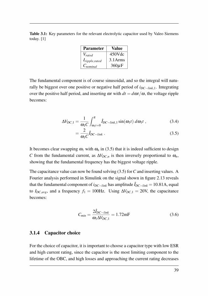
Table 3.1: Key parameters for the relevant electrolytic capacitor used by Valeo Siemenstoday. [1]
Parameter ValueVrated 450VdcIripple,rated 3.1ArmsCnominal 360µF
The fundamental component is of course sinusoidal, and so the integral will natu-rally be biggest over one positive or negative half period of iDC−link,1. Integratingover the positive half period, and inserting ωt with dt = dωt/ω , the voltage ripplebecomes:
∆VDC,1 =1
ω1C
∫π
ω1t=0IDC−link,1 sin(ω1t) dω1t , (3.4)
=2
ω1CIDC−link . (3.5)
It becomes clear swapping ω1 with ωn in (3.5) that it is indeed sufficient to designC from the fundamental current, as ∆VDC,n is then inversely proportional to ωn,showing that the fundamental frequency has the biggest voltage ripple.
The capacitance value can now be found solving (3.5) for C and inserting values. AFourier analysis performed in Simulink on the signal shown in figure 2.13 revealsthat the fundamental component of iDC−link has amplitude IDC−link = 10.81A, equalto IDC,avg, and a frequency f1 = 100Hz. Using ∆VDC,1 = 20V, the capacitancebecomes:
Cmin =2IDC−link
ω1∆VDC,1= 1.72mF (3.6)
3.1.4 Capacitor choice
For the choice of capacitor, it is important to choose a capacitor type with low ESRand high current rating, since the capacitor is the most limiting component to thelifetime of the OBC, and high losses and approaching the current rating decreases
39
the lifetime of the capacitors. A good way of solving this is connecting severalcapacitors in parallel, reducing the current and losses in each of the capacitors. Tomatch the lifetime of the current OBC technology at Valeo Siemens, it is chosen touse the same capacitor. Due to confidenciality the exact model name or datasheetcan not be shown in this thesis, but it is an electrolytic capacitor, and some of itskey parameters are summarized in table 3.1.
With the given Cnominal = 360µF it is apparent that 5 capacitors connected in par-allel is required to match the required minimum capacitance value in (3.6), givingtotal capacitance
C = 5 ·360µF = 1.8mF .
Checking the RMS current through each of the capacitors, the total DC-link RMScurrent can first be found from (2.34). Assuming close-to-zero phase angle φAB dueto the low inductance and using minimum DC-link voltage and maximum powerfor maximum DC-link current, the DC-link RMS current becomes
IDC−link =
√8 ·325V
3π ·340V(16A)2− (10.8A)2 = 9.54A .
Acknowledging that the current in each of the capacitors will be one fifth of thetotal DC-link RMS current, the RMS current through each of the capacitors willbe
IDC−link,cap =15·9.54A = 1.9A ,
which is well below the maximum rated ripple current of the relevant capacitor intable 3.1.
No ESR is given in the datasheet, but with three capacitors connected in parallel,and at the same power level, Valeo Siemens experience power losses < 0.5W ,which is negligible. In this case, with five capacitors connected in parallel, thelosses will be even lower due to lower currents through each of the capacitors. Thislower current stress in each of the capacitors should also imply a longer lifetimeexpectancy of the charger.
40
3.2 Transistors
The right choice of transistors is a key part of the design of any switch-mode con-verter. In this case, the transistors are chosen along with the switching frequencyto comply with the desired efficiency of the whole charger. Moreover, the tran-sistors have to withstand the expected RMS currents, peak blocking voltages andpeak currents. Aided by a heat sink, the transistors should also be able to handleits own dissipated heat without melting.
In the following, the design process for choosing and dimensioning the totem-legand rectifier-leg transistors will be described chronologically. The reason for thisis that converter design is an iterative process, making assumptions and updatingthem based on the results throughout the design process. While dimensioningthe totem-leg transistors, the switching frequency, fsw will also be chosen. Thisbecause the transistors will be designed to match the required efficiency, requiringthe switching losses to be within the allowed losses restriction that follows thisefficiency.
3.2.1 Choice of transistor technology
Totem-leg transistors
When choosing the transistor technology for each of the switches it is important tofirst evaluate the requirements of the switch. First of all, figures 2.2 and 2.3 showthat the current should be able to flow in both directions through all of the switches.Secondly, the totem-leg switches need to be able to handle high-frequency switch-ing, preferably around 100kHz (appendix A), while also keeping the losses suf-ficiently low to comply with the efficiency requirement of 98% in G2V and 97%in V2G. A high switching frequency has several benefits regarding especially thepower density of the OBC; it minimizes the size of magnetic-core components, asis shown further for the boost inductor in section 3.3, and it minimizes the size ofthe AC-side direct mode (DM) filter required to comply with the grid-side currentnoise limitations, declared in the design specifications in appendix A.
In this frequency range, and at a required rating of around ∼400V and ∼22.5A,two transistor technologies stand out as promising solutions: Power MOSFETs
41
and GaN HEMTs. MOSFETs and GaN HEMTs both have bidirectional conduc-tion capability by nature, due to their symmetrical structure.[38] This is beneficial,as it would be sufficient the transistor as the only semiconductor component ineach of ST 1 and ST 2. Furthermore, they are both efficient at high switching levels,much due to the lack of minority carriers having to be moved in and out of thetransistor during switching, as is the case in many other transistor technologies,such as IGBTs and BJTs. [24] However, there are differences in the performanceof these two transistor technologies when working as totem-leg switches, owing totheir structural differences highlighted in [38]. This is also explained in more detailin the paper written on GaN HEMTs in appendix C, and the following argumenta-tion on GaN HEMTs is based on the contents of this paper. The paper states thatalthough GaN as a material has higher breakdown field and band gap than SiC andSi, which initially gives a higher resistivity in the transistor, the two-dimensionalelectron gas (2DEG) layer ensures that the GaN HEMT has a lower RDS,on thanMOSFETs for the same breakdown voltage. Moreover, the higher breakdown fieldof GaN allows for smaller physical embodiments of the transistors compared to Siand SiC MOSFETs at the same rated breakdown voltage, again giving smaller par-asitic capacitances and thus faster switching transients and lower switching losses.Another significant advantage of the GaN HEMT is that, unlike MOSFETs, it doesnot have a reverse body diode. According to [25], the reverse recovery losses ofthe MOSFET reverse body diodes during CCM operation of a totem-pole PFC aresevere, and thus the lack of reverse body diodes in GaN HEMTs is beneficial withregard to losses.
However, one drawback of the GaN HEMT, besides it being a relatively new andthus not fully developed and commercialized technology, is that it has a relativelylow thermal conductivity compared to Si and SiC MOSFETs. That means it willhave trouble dissipating the heat generated from losses, possibly imposing somechallenges in the heat sink design. On the other hand, the results from [39] sug-gest that the performance of GaN HEMTs are less affected by the case tempera-ture, and so the decreased thermal conductivity might not matter anyway. Anotherdrawback is that the GaN HEMT technology is by nature normally-on, meaning itis conducting at low gate voltage, as explained in appendix. This is undesirable,as we want the transistor to be open when the system is not energized. There-fore, it is compensated by constructing normally-off enhancement-mode HEMTs
42
(eHEMTs), either by changing the structure or by cascading a FET at the gate ofthe HEMT. This derates the switching performance of the GaN HEMT some, butstill it is an improvement compared to existing technology in that regard.
All of this taken into account, the GaN eHEMT is chosen as the transistor technol-ogy for use in the totem-leg switches. This is because it appears most efficient inhigh-frequency and high-power application. This decision is backed up by calcu-lations in section 3.2.5.
Rectifier-leg transistors
As for the rectifier-leg switches, these only really have one requirement, which isbidirectional conduction ability, due to the reverse direction of the current in V2Gmode shown in figure 2.3. The switching losses are negligible, due to a switchingfrequency equal to the mains frequency (45Hz-65Hz), and thus it is desirable tohave transistors with low conduction losses. In that sense, it will be sufficientto use slow-switching low-RDS,on MOSFETs. Since a more advanced transistortechnology has been used in the totem-leg switches, it also becomes a questionof price, especially since the OBC would be mass-produced. Thus a cheaper andsimpler MOSFET, just complying with the loss and rating demands is preferablein the rectifier-leg switches.
Corresponding topology
The updated bidirectional totem-pole PFC topology, with GaN eHEMTs in thetotem leg and MOSFETs in the rectifier leg, is shown in figure 3.2. Due to theabsence of eHEMT symbols in the drawing software, eHEMTs are represented asMOSFETs with no reverse diodes.
3.2.2 Guesstimating component loss distribution
As specified in the bidirectional OBC and PFC specifications in tables 1.1 and 1.2,the efficiency of an OBC should be designed at 94% in G2V charging mode, withthe efficiency of the PFC being at 98% for the standard voltage levels (230Vrms
43
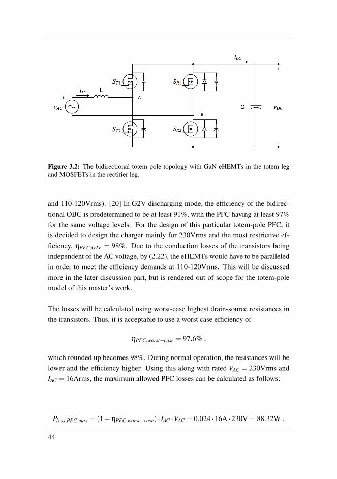
Figure 3.2: The bidirectional totem pole topology with GaN eHEMTs in the totem legand MOSFETs in the rectifier leg.
and 110-120Vrms). [20] In G2V discharging mode, the efficiency of the bidirec-tional OBC is predetermined to be at least 91%, with the PFC having at least 97%for the same voltage levels. For the design of this particular totem-pole PFC, itis decided to design the charger mainly for 230Vrms and the most restrictive ef-ficiency, ηPFC,G2V = 98%. Due to the conduction losses of the transistors beingindependent of the AC voltage, by (2.22), the eHEMTs would have to be paralleledin order to meet the efficiency demands at 110-120Vrms. This will be discussedmore in the later discussion part, but is rendered out of scope for the totem-polemodel of this master’s work.
The losses will be calculated using worst-case highest drain-source resistances inthe transistors. Thus, it is acceptable to use a worst case efficiency of
ηPFC,worst−case = 97.6% ,
which rounded up becomes 98%. During normal operation, the resistances will belower and the efficiency higher. Using this along with rated VAC = 230Vrms andIAC = 16Arms, the maximum allowed PFC losses can be calculated as follows:
Ploss,PFC,max = (1−ηPFC,worst−case) · IAC ·VAC = 0.024 ·16A ·230V = 88.32W .
44
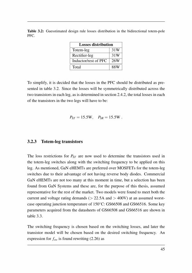
Table 3.2: Guesstimated design rule losses distribution in the bidirectional totem-polePFC.
Losses distributionTotem-leg 31WRectifier-leg 31WInductor/rest of PFC 26WTotal 88W
To simplify, it is decided that the losses in the PFC should be distributed as pre-sented in table 3.2. Since the losses will be symmetrically distributed across thetwo transistors in each leg, as is determined in section 2.4.2, the total losses in eachof the transistors in the two legs will have to be:
PST = 15.5W, PSR = 15.5W .
3.2.3 Totem-leg transistors
The loss restrictions for PST are now used to determine the transistors used inthe totem-leg switches along with the switching frequency to be applied on thisleg. As mentioned, GaN eHEMTs are preferred over MOSFETs for the totem-legswitches due to their advantage of not having reverse body diodes. CommercialGaN eHEMTs are not too many at this moment in time, but a selection has beenfound from GaN Systems and these are, for the purpose of this thesis, assumedrepresentative for the rest of the market. Two models were found to meet both thecurrent and voltage rating demands (> 22.5A and > 400V) at an assumed worst-case operating junction temperature of 150C: GS66508 and GS66516. Some keyparameters acquired from the datasheets of GS66508 and GS66516 are shown intable 3.3.
The switching frequency is chosen based on the switching losses, and later thetransistor model will be chosen based on the desired switching frequency. Anexpression for fsw is found rewriting (2.26) as
45

Table 3.3: Some key parameters and rated values of the GaN Systems eHEMTs at Tcase =25C.
Parameter GS66508 GS66516RDS,on 50mΩ 25mΩ
RDS,on (@150C) 129mΩ 67mΩ
QG 5.8 nC 12nCVDS 650V 650VVGS -10V to +7V -10V to +7VIDS 30A 60AIDS (@100C) 25A 47A
Switching energy with VDS = 400VEon,rated 47.5µJ (@15A) 134.1µJ (@20A)Eo f f ,rated 7.5µJ (@15A) 14.7µJ (@20A)
fsw =Psw
Esw. (3.7)
The switching energy is calculated from the values in table 3.3, while Psw is foundfrom
Psw = Ptransistor−Pcond , (3.8)
where Ptransistor is given from the design rules, and Pcond is calculated using (2.22).As with the drain-source current capability, since the RDS,on of MOSFETs andeHEMTs increase for increasing temperature, the worst-case 150C on-state re-sistance must be considered when computing the expected conduction losses, asit will give the biggest losses. Applying the RDS,on at 150C listed in table 3.3and IAC = 16A to (2.22), the conduction losses of each of the eHEMT models arecalculated as shown in table 3.4. The results show that the conduction losses ofGS66508 have conduction losses that are higher than the permitted totem-leg tran-sistor losses. That leaves GS66516 as the only real option, and this GaN eHEMTis chosen for the totem-leg switches.
46
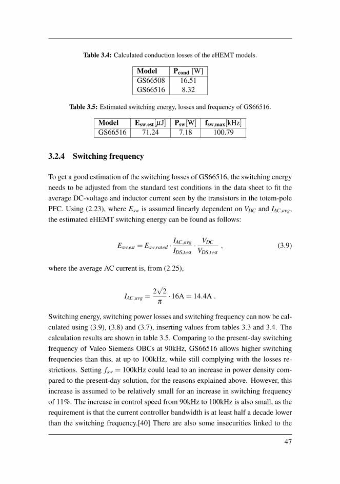
Table 3.4: Calculated conduction losses of the eHEMT models.
Model Pcond [W]GS66508 16.51GS66516 8.32
Table 3.5: Estimated switching energy, losses and frequency of GS66516.
Model Esw,est[µJ] Psw[W] fsw,max[kHz]GS66516 71.24 7.18 100.79
3.2.4 Switching frequency
To get a good estimation of the switching losses of GS66516, the switching energyneeds to be adjusted from the standard test conditions in the data sheet to fit theaverage DC-voltage and inductor current seen by the transistors in the totem-polePFC. Using (2.23), where Esw is assumed linearly dependent on VDC and IAC,avg,the estimated eHEMT switching energy can be found as follows:
Esw,est = Esw,rated ·IAC,avg
IDS,test· VDC
VDS,test, (3.9)
where the average AC current is, from (2.25),
IAC,avg =2√
2π·16A = 14.4A .
Switching energy, switching power losses and switching frequency can now be cal-culated using (3.9), (3.8) and (3.7), inserting values from tables 3.3 and 3.4. Thecalculation results are shown in table 3.5. Comparing to the present-day switchingfrequency of Valeo Siemens OBCs at 90kHz, GS66516 allows higher switchingfrequencies than this, at up to 100kHz, while still complying with the losses re-strictions. Setting fsw = 100kHz could lead to an increase in power density com-pared to the present-day solution, for the reasons explained above. However, thisincrease is assumed to be relatively small for an increase in switching frequencyof 11%. The increase in control speed from 90kHz to 100kHz is also small, as therequirement is that the current controller bandwidth is at least half a decade lowerthan the switching frequency.[40] There are also some insecurities linked to the
47
estimation of switching energy, due to the rough approximation in (2.24), makingit sensible to choose a lower frequency than the maximum of 100kHz. Moreover,the objective of this master’s thesis is to reveal whether the bidirectional totem-pole PFC is suiting for a bidirectional OBC, rather than optimizing with respectto size. Therefore, for simplicity, it is chosen to proceed with the same switch-ing frequency as in the present-day solutions of Valeo Siemens, assuming that theincreased number of gate drivers required for the totem-pole and the altered re-quired heat sink design does not propose a big increase in the power density ofthe hardware OBC solution. That way, e.g. the same type of DC-link capacitorand inductor could be used in this solution, since these see the same currents andvoltages for a totem-pole as for a regular boost PFC. The same AC-side DM fil-ter could also be used, although the filtering is out of scope for this thesis. Theswitching frequency is set at
fsw = 90kHz .
3.2.5 Comparison to state-of-the-art MOSFETs
Comparing to the state-of-the-art lowest-RDS,on power MOSFETs on the marketwith a rating of at least 400Vdc and 25Adc, such as Infineon’s automotive powerMOSFET IPW60R045CPA, these have a rated RDS,on = 45mΩ. Scaling to a worst-case on-state resistance at 150C from the data sheet of IPW60R045CPA, thisbecomes 110mΩ, which using (2.22) gives conduction losses
Pcond,MOS =12· (16A)2 ·110mΩ = 14W .
An estimation of the MOSFET switching energy using (2.24) and data for switch-ing times from the data sheet of IPW60R045CPA gives
Esw,MOS,noRR =12·30ns ·340V ·14.4A = 73.44µJ ,
when not considering the reverse recovery losses of the body diode. That gives amaximum switching frequency, not considering reverse recovery losses, using the
48
same procedure as for the GaN eHEMTs:
fsw,MOS,max,noRR = 20.42kHz .
If the reverse recovery losses were considered, this switching frequency would beeven lower. In fact, it is found that [30] that the switching losses of a superjunctionCoolMOS has 20 times more switching loss when operated in the totem-leg, dueto the reverse recovery diode. This should make the GaN eHEMT GS66516 a farsuperior solution to the IPW60R045CPA.
However, it is worth noting that this analysis is not sufficient for concluding withabsolute certainty that the GaN eHEMT is in fact the best solution, as especiallythe estimated switching losses are based on possibly rough approximations fromuncertain parameters in the component data sheets. To get a proper overview of thelosses in each of the transistors, tests should be performed, measuring the lossesin each of the transistors at the relevant current and voltage operating point, e.g.using thermal measurement equipment. Nonetheless, GaN eHEMTs are, basedon this switching and conduction loss analysis, considered the best solution, andGS66516 will be the transistor of choice for use in the high-frequency totem leg.
3.2.6 Rectifier-leg transistors
For the rectifier-leg transistors, the switching frequency will be equal to the mainsfrequency, meaning switching losses are negligible. Therefore, all that is requiredfor the rectifier-leg transistors is bidirectional conduction ability and low conduc-tion losses. A good choice for these transistors would thus be slow-switchingMOSFETs with a low RDS,on. Rearranging (2.22) and setting Pcond,SR,max = PSR =
17W, the span of allowed RDS,on for the rectifier-leg mosfets can be found as fol-lows:
RDS,on,SR ≤ 2Pcond,SR,max
I2AC
= 132.8mΩ (3.10)
Thus, any MOSFET with an RDS,on ≤ 132.8mΩ, voltage rating > 400V and drain-source current capability > 22.5A would be suiting for this solution. A quick
49

Table 3.6: Some key parameters and rated values of MOSFET IPW60R045CPA at Tcase =25C.
Parameter ValueRDS,on 45mΩ
RDS,on (@150C) 110mΩ
VDS 600VVGS -20V to +20VIDS 60AIDS (@100C) 38AVSD (Diode FV) 0.9V
search reveals many possible solutions, but Infineon’s previously analyzed auto-motive MOSFET IPW60R045CPA is chosen, with key parameters shown in table3.6.
50
3.3 Boost inductor
Design of magnetic components for power electronics is a research field of its own,and an overview of the challenges faced can be found in [24, ch. 30]. For the sakeof this master’s thesis, when designing the boost inductor, the magnetic designitself is regarded out of scope. The design process will revolve around choosingfrom existing inductor technologies, considering mainly three factors: Inductancevalue, RMS current rating and peak current rating.
3.3.1 Boost inductance value
The boost inductance value L, along with the magnitudes of vAC and Vd , dictatesthe slope of the inductor current in every switching interval according to (2.1)and (2.2). These equations imply that a higher switching frequency would requirea smaller inductance for the same maximum ripple, and likewise with a highermaximum ripple for the same frequency, as both of these cases would increase therequired slope. For that reason the boost inductance, L, needs to be designed smallenough to allow for the desired switching frequency and large enough limit thecurrent ripple to its maximum allowed value.
The equations for the inductor ripple is developed in section 2.3.1. It is shown in(2.6) that the ripple is proportional to the DC-link voltage, meaning the maximuminductor current ripple occurs at the maximum DC-link voltage. Figure 2.5 alsoshows that the maximum inductor current ripple occurs at duty cycle d = 0.5. Us-ing this information, an expression for maximum inductor current ripple is foundfrom (2.6):
∆iL,max =0.25VDC,max
fswL. (3.11)
Solving (3.11) for L, an expression is developed for the boost inductance value:
L =0.25VDC,max
fsw∆iL,max. (3.12)
Defining the AC-side current ripple to be set at 20% of peak AC current accord-
51
ing to the bidirectional PFC specifications presented in table 1.2, the maximumcurrent ripple becomes ∆iL,max = 0.2 · Iac = 4.52 A. The switching frequency hasbeen chosen at fsw = 90kHz and the maximum DC-link voltage is VDC,max = 400V.Inserting these data in (3.12), the resulting value of the boost inductance is foundto be:
L≥ 245.82µH .
3.3.2 RMS current rating
Overly high RMS currents in magnetic core inductors can lead to saturation ofits core material or overheating due to resistive losses in the windings and eddycurrent losses in the core.[24, ch. 30] Thus, the inductor needs to be designedwith sufficient RMS current rating. It is found in section 2.3.2 and (2.11) that theRMS current in the inductor is equal to the AC-grid RMS current. That meansthe inductor current rating should comply with the AC current rating described intable 1.1, giving the following inductor RMS current rating:
IL,rated = 16A .
3.3.3 Saturation current rating
Although continuous currents can cause magnetic core saturation in the inductor,this is a more adjacent issue with the peak currents, especially in switch-modeconverters, where a current ripple is in fact necessary to control the output andinput currents and voltages. [24, ch. 30] The maximum peak-to-peak currentripple is defined in table 1.2, to be 20% of the peak current value. Using that, theminimum peak current rating of the inductor can be defined as follows:
IL,sat = (1+0.1)√
2IAC,max = 24.89A
52

Table 3.7: Estimated inductor parameters based on technology used by Valeo Siemenstoday.[1]
Parameter ValueL 245.82µHRL 10mΩ
Irated 16ArmsPloss,est(100C) 17W
3.3.4 Choice of inductor
Unlike the capacitor and transistors, who are mostly off-the-shelf components,the inductor is a more easily customizable component, where performance for aninductor with a certain core design is dependent on e.g. number of windings thick-ness of windings.[24] For this application and for the sake of the simulation modelit is chosen to use the same inductor technology as is used by Valeo Siemens to-day, assuming that windings are chosen to achieve exactly the desired inductance.The inductor is powder-core, toroid-shaped with copper wires, and reasonable pa-rameters based on this technology are presented in table 3.7.[1] Saturation currentrating is not mentioned in the data sheet. The data for estimated power losses arefound in data sheets, and comparing it to table 3.7 it is clear that it does not exceedthe estimated losses of the inductor and rest of PFC.
53

54
Chapter 4Drive and control
In a PFC, as in any other switched-mode converter, the control system and gatedrivers are essential to its operation; they govern the average current through - andvoltage across - the switches, controlling currents and voltages in the rest of theconverter.[24, ch. 28] Control-wise, a PFC has two objectives: It needs to controlthe AC current to be sinusoidal and in phase with the AC voltage, and it needs tocontrol the average value of the DC-side voltage. In the following, the gate driverlogic and the control system will be developed for the ideal proposed bidirectionaltotem-pole PFC converter, to build the simulation model and verify the basic op-eration of this converter. The control system will be built using average currentmode control.[41, 42, 43] Current and voltage control loops will be analyzed sepa-rately and designed with PI controllers and symmetrical optimum tuning.[44] TheMATLAB scripts used for tuning are shown in appendix F. The practical imple-mentation of the gate drivers will be neglected for this analysis.
55
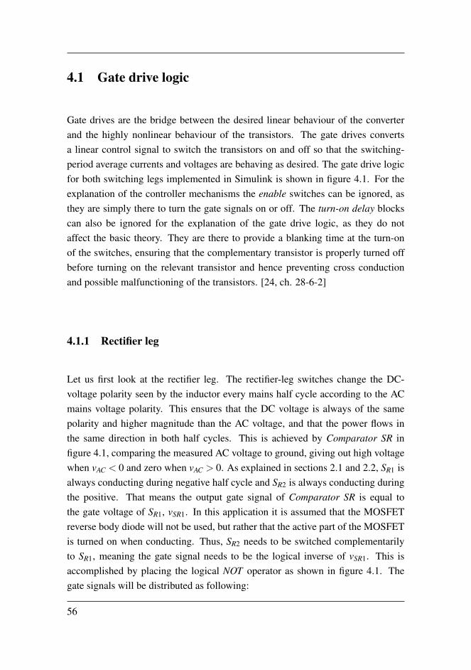
4.1 Gate drive logic
Gate drives are the bridge between the desired linear behaviour of the converterand the highly nonlinear behaviour of the transistors. The gate drives convertsa linear control signal to switch the transistors on and off so that the switching-period average currents and voltages are behaving as desired. The gate drive logicfor both switching legs implemented in Simulink is shown in figure 4.1. For theexplanation of the controller mechanisms the enable switches can be ignored, asthey are simply there to turn the gate signals on or off. The turn-on delay blockscan also be ignored for the explanation of the gate drive logic, as they do notaffect the basic theory. They are there to provide a blanking time at the turn-onof the switches, ensuring that the complementary transistor is properly turned offbefore turning on the relevant transistor and hence preventing cross conductionand possible malfunctioning of the transistors. [24, ch. 28-6-2]
4.1.1 Rectifier leg
Let us first look at the rectifier leg. The rectifier-leg switches change the DC-voltage polarity seen by the inductor every mains half cycle according to the ACmains voltage polarity. This ensures that the DC voltage is always of the samepolarity and higher magnitude than the AC voltage, and that the power flows inthe same direction in both half cycles. This is achieved by Comparator SR infigure 4.1, comparing the measured AC voltage to ground, giving out high voltagewhen vAC < 0 and zero when vAC > 0. As explained in sections 2.1 and 2.2, SR1 isalways conducting during negative half cycle and SR2 is always conducting duringthe positive. That means the output gate signal of Comparator SR is equal tothe gate voltage of SR1, vSR1. In this application it is assumed that the MOSFETreverse body diode will not be used, but rather that the active part of the MOSFETis turned on when conducting. Thus, SR2 needs to be switched complementarilyto SR1, meaning the gate signal needs to be the logical inverse of vSR1. This isaccomplished by placing the logical NOT operator as shown in figure 4.1. Thegate signals will be distributed as following:
56
Figure 4.1: A screenshot of the PWM system implemented in Simulink.
57
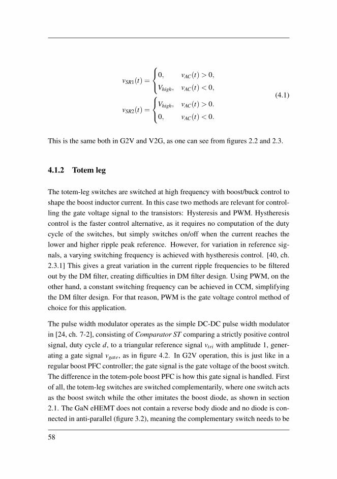
vSR1(t) =
0, vAC(t)> 0,
Vhigh, vAC(t)< 0,
vSR2(t) =
Vhigh, vAC(t)> 0.
0, vAC(t)< 0.
(4.1)
This is the same both in G2V and V2G, as one can see from figures 2.2 and 2.3.
4.1.2 Totem leg
The totem-leg switches are switched at high frequency with boost/buck control toshape the boost inductor current. In this case two methods are relevant for control-ling the gate voltage signal to the transistors: Hysteresis and PWM. Hystheresiscontrol is the faster control alternative, as it requires no computation of the dutycycle of the switches, but simply switches on/off when the current reaches thelower and higher ripple peak reference. However, for variation in reference sig-nals, a varying switching frequency is achieved with hystheresis control. [40, ch.2.3.1] This gives a great variation in the current ripple frequencies to be filteredout by the DM filter, creating difficulties in DM filter design. Using PWM, on theother hand, a constant switching frequency can be achieved in CCM, simplifyingthe DM filter design. For that reason, PWM is the gate voltage control method ofchoice for this application.
The pulse width modulator operates as the simple DC-DC pulse width modulatorin [24, ch. 7-2], consisting of Comparator ST comparing a strictly positive controlsignal, duty cycle d, to a triangular reference signal vtri with amplitude 1, gener-ating a gate signal vgate, as in figure 4.2. In G2V operation, this is just like in aregular boost PFC controller; the gate signal is the gate voltage of the boost switch.The difference in the totem-pole boost PFC is how this gate signal is handled. Firstof all, the totem-leg switches are switched complementarily, where one switch actsas the boost switch while the other imitates the boost diode, as shown in section2.1. The GaN eHEMT does not contain a reverse body diode and no diode is con-nected in anti-parallel (figure 3.2), meaning the complementary switch needs to be
58
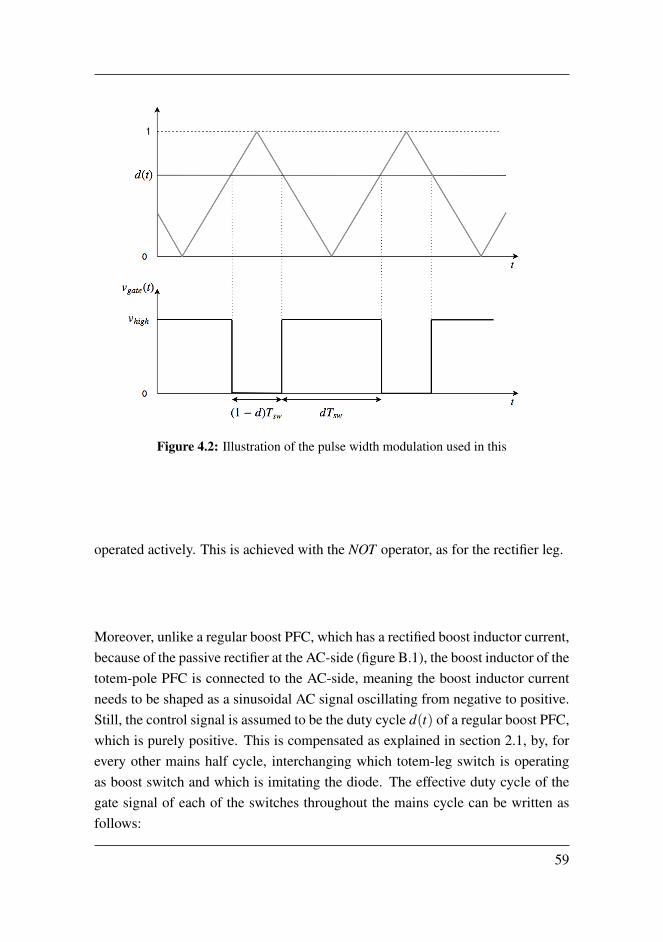
Figure 4.2: Illustration of the pulse width modulation used in this
operated actively. This is achieved with the NOT operator, as for the rectifier leg.
Moreover, unlike a regular boost PFC, which has a rectified boost inductor current,because of the passive rectifier at the AC-side (figure B.1), the boost inductor of thetotem-pole PFC is connected to the AC-side, meaning the boost inductor currentneeds to be shaped as a sinusoidal AC signal oscillating from negative to positive.Still, the control signal is assumed to be the duty cycle d(t) of a regular boost PFC,which is purely positive. This is compensated as explained in section 2.1, by, forevery other mains half cycle, interchanging which totem-leg switch is operatingas boost switch and which is imitating the diode. The effective duty cycle of thegate signal of each of the switches throughout the mains cycle can be written asfollows:
59

dST 1(t) =
1−d(t), vAC(t)> 0,
d(t), vAC(t)< 0,
dST 2(t) =
d(t), vAC(t)> 0.
1−d(t), vAC(t)< 0.
(4.2)
Acknowledging that for high switching frequencies fsw fAC with gate voltageamplitudes of Vhigh = 1 in figure 4.2, the duty cycles can be written as follows:
d(t) = vgate,avg(t) , dST 1(t) = vST 1,avg(t) , dST 2(t) = vST 2,avg, (4.3)
where vgate,avg, vST 1,avg and vST 2,avg are the floating switching-period averages ofvgate, vST 1 and vST 2. Applying (4.3) to (4.2), it can be shown that the totem-legswitches gate voltages can be written as follows:
vST 1(t) =
1− vgate(t), vAC(t)> 0,
vgate(t), vAC(t)< 0,
vST 2(t) =
vgate(t), vAC(t)> 0.
1− vgate(t), vAC(t)< 0.
(4.4)
The gate voltages are logical signals of true or false, in this case 1 or 0. Thus,it is clear that the negative-half-cycle gate signals can be achieved by logicallyinverting the positive-half-cycle gate signals. To perform this logical inversion, ahandy way of rewriting the gate voltages during negative half cycle can be:
vST 1(t) = vgate(t) = 1−|vgate(t)−1| , vAC(t)< 0 ,
vST 2(t) = 1− vgate(t) = |vgate(t)−1| , vAC(t)< 0 .(4.5)
The equation (4.5) puts the negative-half-cycle gate signals on the same form,
60

vST 1 = 1−u and vST 2 = u, as the positive-half-cycle signals in (4.4). Now, all thatneeds to be handled is u, which is either vgate or |vgate−1|, depending on the mainshalf cycle. Using (4.5) and recognizing from (4.1), with Vhigh = 1, that vSR1 is 0for vAC > 0 and 1 for vAC < 0, a simple way of handling u and creating the desiredgate voltages in (4.4) can be the following:
vST 1(t) = 1−|vgate(t)− vSR1(t)| ,vST 2(t) = |vgate(t)− vSR1(t)| .
(4.6)
This is implemented in figure 4.1 with the forward connection from the rectifier-legsystem to the totem-leg system.
V2G
In V2G, the PFC operates as a buck converter from DC-link to grid, in stead of as aboost converter from grid to DC-link. However, comparing the AC to DC voltageratios based on the duty cycle definitions of buck and boost operation, [24, ch. 7]
vAC(t)VDC
=
dbuck(t) for buck operation ,
1−dboost(t) for boost operation ,(4.7)
it is clear that dbuck = 1− dboost = 1− d, i.e. that the boost and buck switchingare complementary to each other. Thus, since the figures 2.2 and 2.3 show that thebuck switch is always the complementary switch to the boost switch, the totem-leggate voltages during V2G are also controlled by (4.2) and (4.6). In other words,the shape and phase of the gate voltages do not change during V2G
4.1.3 Waveforms
For verification of the gate drive operation a simulation is performed, with resultsshown in figure 4.3. It shows the duty cycle d, the triangular voltage vtri and thegate voltages VST 1, VST 2, VSR1 and VSR2 in G2V operation, which is the same for
61
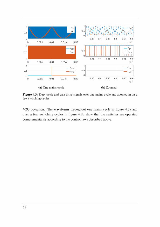
(a) One mains cycle (b) Zoomed
Figure 4.3: Duty cycle and gate drive signals over one mains cycle and zoomed in on afew switching cycles.
V2G operation. The waveforms throughout one mains cycle in figure 4.3a andover a few switching cycles in figure 4.3b show that the switches are operatedcomplementarily according to the control laws described above.
62
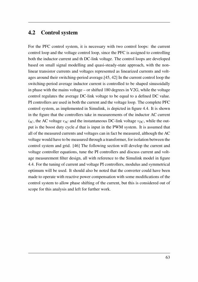
4.2 Control system
For the PFC control system, it is necessary with two control loops: the currentcontrol loop and the voltage control loop, since the PFC is assigned to controllingboth the inductor current and th DC-link voltage. The control loops are developedbased on small signal modelling and quasi-steady-state approach, with the non-linear transistor currents and voltages represented as linearized currents and volt-ages around their switching-period average.[45, 42] In the current control loop theswitching-period average inductor current is controlled to be shaped sinusoidallyin phase with the mains voltage – or shifted 180 degrees in V2G, while the voltagecontrol regulates the average DC-link voltage to be equal to a defined DC value.PI controllers are used in both the current and the voltage loop. The complete PFCcontrol system, as implemented in Simulink, is depicted in figure 4.4. It is shownin the figure that the controllers take in measurements of the inductor AC currentiAC, the AC voltage vAC and the instantaneous DC-link voltage vDC, while the out-put is the boost duty cycle d that is input in the PWM system. It is assumed thatall of the measured currents and voltages can in fact be measured, although the ACvoltage would have to be measured through a transformer, for isolation between thecontrol system and grid. [46] The following section will develop the current andvoltage controller equations, tune the PI controllers and discuss current and volt-age measurement filter design, all with reference to the Simulink model in figure4.4. For the tuning of current and voltage PI controllers, modulus and symmetricaloptimum will be used. It should also be noted that the converter could have beenmade to operate with reactive power compensation with some modifications of thecontrol system to allow phase shifting of the current, but this is considered out ofscope for this analysis and left for further work.
63
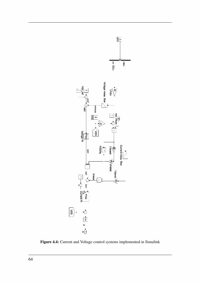
Figure 4.4: Current and Voltage control systems implemented in Simulink
64
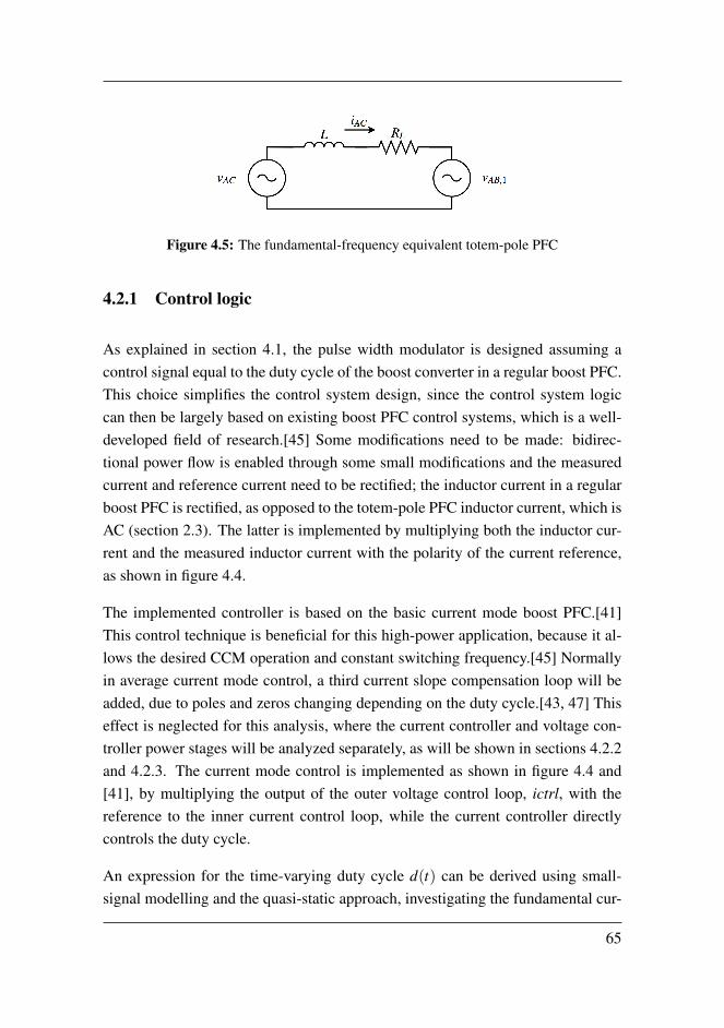
Figure 4.5: The fundamental-frequency equivalent totem-pole PFC
4.2.1 Control logic
As explained in section 4.1, the pulse width modulator is designed assuming acontrol signal equal to the duty cycle of the boost converter in a regular boost PFC.This choice simplifies the control system design, since the control system logiccan then be largely based on existing boost PFC control systems, which is a well-developed field of research.[45] Some modifications need to be made: bidirec-tional power flow is enabled through some small modifications and the measuredcurrent and reference current need to be rectified; the inductor current in a regularboost PFC is rectified, as opposed to the totem-pole PFC inductor current, which isAC (section 2.3). The latter is implemented by multiplying both the inductor cur-rent and the measured inductor current with the polarity of the current reference,as shown in figure 4.4.
The implemented controller is based on the basic current mode boost PFC.[41]This control technique is beneficial for this high-power application, because it al-lows the desired CCM operation and constant switching frequency.[45] Normallyin average current mode control, a third current slope compensation loop will beadded, due to poles and zeros changing depending on the duty cycle.[43, 47] Thiseffect is neglected for this analysis, where the current controller and voltage con-troller power stages will be analyzed separately, as will be shown in sections 4.2.2and 4.2.3. The current mode control is implemented as shown in figure 4.4 and[41], by multiplying the output of the outer voltage control loop, ictrl, with thereference to the inner current control loop, while the current controller directlycontrols the duty cycle.
An expression for the time-varying duty cycle d(t) can be derived using small-signal modelling and the quasi-static approach, investigating the fundamental cur-
65
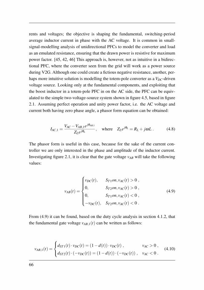
rents and voltages; the objective is shaping the fundamental, switching-periodaverage inductor current in phase with the AC voltage. It is common in small-signal-modelling analysis of unidirectional PFCs to model the converter and loadas an emulated resistance, ensuring that the drawn power is resistive for maximumpower factor. [45, 42, 46] This approach is, however, not as intuitive in a bidirec-tional PFC, where the converter seen from the grid will work as a power sourceduring V2G. Although one could create a fictious negative resistance, another, per-haps more intuitive solution is modelling the totem-pole converter as a VDC-drivenvoltage source. Looking only at the fundamental components, and exploiting thatthe boost inductor in a totem-pole PFC in on the AC side, the PFC can be equiv-alated to the simple two-voltage-source system shown in figure 4.5, based in figure2.1. Assuming perfect operation and unity power factor, i.e. the AC voltage andcurrent both having zero phase angle, a phasor form equation can be obtained:
IAC,1 =VAC−VAB,1e jθAB,1
ZLe jθL, where ZLe jθL = RL + jωL . (4.8)
The phasor form is useful in this case, because for the sake of the current con-troller we are only interested in the phase and amplitude of the inductor current.Investigating figure 2.1, it is clear that the gate voltage vAB will take the followingvalues:
vAB(t) =
vDC(t), ST 1on,vAC(t)> 0 ,
0, ST 2on,vAC(t)> 0 ,
0, ST 1on,vAC(t)< 0 ,
−vDC(t), ST 2on,vAC(t)< 0 .
(4.9)
From (4.9) it can be found, based on the duty cycle analysis in section 4.1.2, thatthe fundamental gate voltage vAB,1(t) can be written as follows:
vAB,1(t) =
dST 1(t) · vDC(t) = (1−d(t)) · vDC(t) , vAC > 0 ,
dST 2(t) · (−vDC(t)) = (1−d(t)) · (−vDC(t)) , vAC < 0 .(4.10)
66
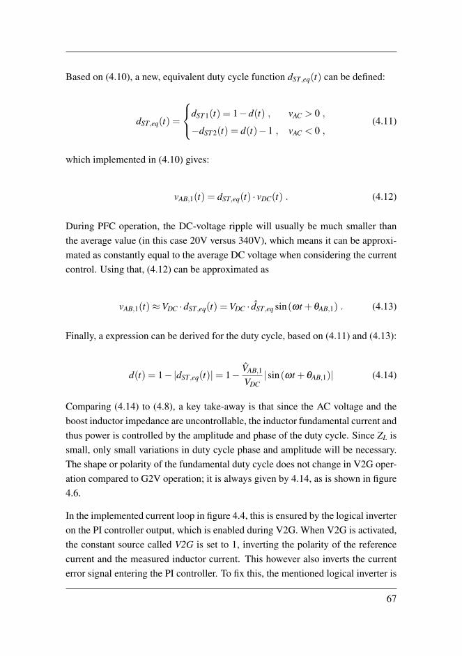
Based on (4.10), a new, equivalent duty cycle function dST,eq(t) can be defined:
dST,eq(t) =
dST 1(t) = 1−d(t) , vAC > 0 ,
−dST 2(t) = d(t)−1 , vAC < 0 ,(4.11)
which implemented in (4.10) gives:
vAB,1(t) = dST,eq(t) · vDC(t) . (4.12)
During PFC operation, the DC-voltage ripple will usually be much smaller thanthe average value (in this case 20V versus 340V), which means it can be approxi-mated as constantly equal to the average DC voltage when considering the currentcontrol. Using that, (4.12) can be approximated as
vAB,1(t)≈VDC ·dST,eq(t) =VDC · dST,eq sin(ωt +θAB,1) . (4.13)
Finally, a expression can be derived for the duty cycle, based on (4.11) and (4.13):
d(t) = 1−|dST,eq(t)|= 1− VAB,1
VDC|sin(ωt +θAB,1)| (4.14)
Comparing (4.14) to (4.8), a key take-away is that since the AC voltage and theboost inductor impedance are uncontrollable, the inductor fundamental current andthus power is controlled by the amplitude and phase of the duty cycle. Since ZL issmall, only small variations in duty cycle phase and amplitude will be necessary.The shape or polarity of the fundamental duty cycle does not change in V2G oper-ation compared to G2V operation; it is always given by 4.14, as is shown in figure4.6.
In the implemented current loop in figure 4.4, this is ensured by the logical inverteron the PI controller output, which is enabled during V2G. When V2G is activated,the constant source called V2G is set to 1, inverting the polarity of the referencecurrent and the measured inductor current. This however also inverts the currenterror signal entering the PI controller. To fix this, the mentioned logical inverter is
67
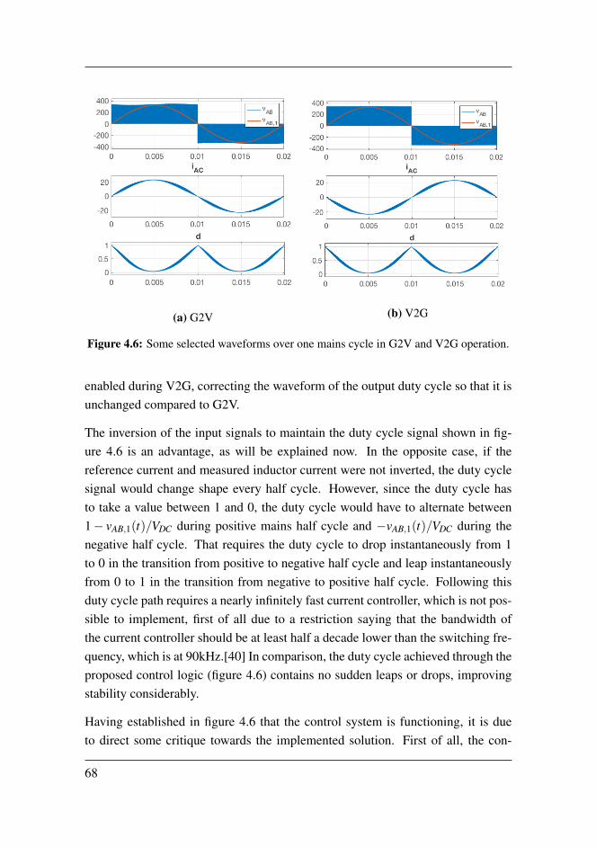
(a) G2V (b) V2G
Figure 4.6: Some selected waveforms over one mains cycle in G2V and V2G operation.
enabled during V2G, correcting the waveform of the output duty cycle so that it isunchanged compared to G2V.
The inversion of the input signals to maintain the duty cycle signal shown in fig-ure 4.6 is an advantage, as will be explained now. In the opposite case, if thereference current and measured inductor current were not inverted, the duty cyclesignal would change shape every half cycle. However, since the duty cycle hasto take a value between 1 and 0, the duty cycle would have to alternate between1− vAB,1(t)/VDC during positive mains half cycle and −vAB,1(t)/VDC during thenegative half cycle. That requires the duty cycle to drop instantaneously from 1to 0 in the transition from positive to negative half cycle and leap instantaneouslyfrom 0 to 1 in the transition from negative to positive half cycle. Following thisduty cycle path requires a nearly infinitely fast current controller, which is not pos-sible to implement, first of all due to a restriction saying that the bandwidth ofthe current controller should be at least half a decade lower than the switching fre-quency, which is at 90kHz.[40] In comparison, the duty cycle achieved through theproposed control logic (figure 4.6) contains no sudden leaps or drops, improvingstability considerably.
Having established in figure 4.6 that the control system is functioning, it is dueto direct some critique towards the implemented solution. First of all, the con-
68

trol circuitry of the average current mode PFC controller is quite complex, witha multiplied voltage loop and current loop. This issue could have been addressedby implementing e.g. linear peak current mode control or other techniques for es-timating the AC voltage, so that the voltage measurement becomes unnecessary.[42, 48] On the other hand, the control system could be implemented digitally, inwhich case the control circuitry would not be as complex. Another issue is thenecessity of measuring the AC voltage through a voltage transformer, implying arisk of low energy density. This issue could also be addressed through the men-tioned AC voltage estimation techniques, not needing to measure the voltage. Inany case, the control structure provides a reference when designing new, improvedcontrol systems for bidirectional PFC converters, using e.g. the techniques men-tioned above.
69
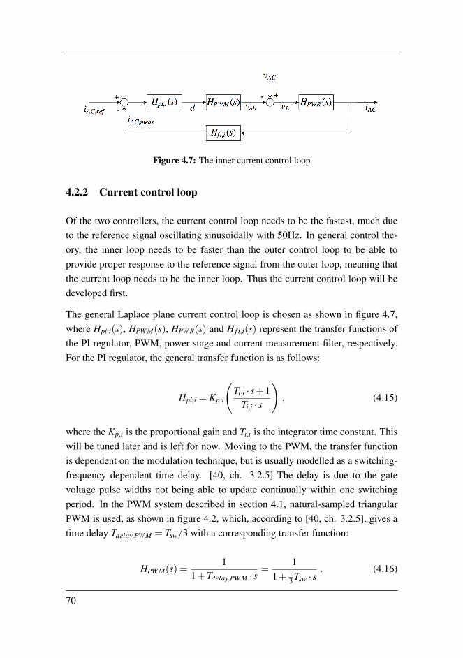
Figure 4.7: The inner current control loop
4.2.2 Current control loop
Of the two controllers, the current control loop needs to be the fastest, much dueto the reference signal oscillating sinusoidally with 50Hz. In general control the-ory, the inner loop needs to be faster than the outer control loop to be able toprovide proper response to the reference signal from the outer loop, meaning thatthe current loop needs to be the inner loop. Thus the current control loop will bedeveloped first.
The general Laplace plane current control loop is chosen as shown in figure 4.7,where Hpi,i(s), HPWM(s), HPWR(s) and H f i,i(s) represent the transfer functions ofthe PI regulator, PWM, power stage and current measurement filter, respectively.For the PI regulator, the general transfer function is as follows:
Hpi,i = Kp,i
(Ti,i · s+1
Ti,i · s
), (4.15)
where the Kp,i is the proportional gain and Ti,i is the integrator time constant. Thiswill be tuned later and is left for now. Moving to the PWM, the transfer functionis dependent on the modulation technique, but is usually modelled as a switching-frequency dependent time delay. [40, ch. 3.2.5] The delay is due to the gatevoltage pulse widths not being able to update continually within one switchingperiod. In the PWM system described in section 4.1, natural-sampled triangularPWM is used, as shown in figure 4.2, which, according to [40, ch. 3.2.5], gives atime delay Tdelay,PWM = Tsw/3 with a corresponding transfer function:
HPWM(s) =1
1+Tdelay,PWM · s=
11+ 1
3 Tsw · s. (4.16)
70

So, to the power stage, which for the current control is approximated as solely theinductor, since the variable to be controlled is the fundamental-harmonic currentthrough the inductor. Referring to figure 2.1, the inductor current IAC(s) can beexpressed in Laplace transform as follows:
iAC(s) =vAC(s)− vab(s)
RL +L · s, (4.17)
where RL is the inductor equivalent resistance. The control variable is the bridgegate voltage VAB(s), while VAC(s) can be seen as a disturbance from the controlpoint of view. Thus, from (4.17), the power-stage transfer function can be written
HPWR(s) =vAC(s)vAB(s)
=1
RL +L · s=
1RL
11+ L
RL· s
. (4.18)
As for the current measurement filter, the purpose of this is to suppress switching-frequency and higher-frequency current noise going into the controller, potentiallymaking the controller generate more harmonics. [40, ch. 3.4] Thus, a simple first-order low-pass filter is evaluated to be sufficient for this application, with transferfunction:
H f i,i(s) =1
1+Tf i,i · s, (4.19)
where Tf i,i is the current measurement filter time constant. Having establishedthese transfer functions, the open-loop current controller transfer function becomes
Hol,i(s) = Hpi,i ·HPWM(s) ·HPWR(s) ·H f i,i(s) ,
=Kp,i
Ti,iRL· 1+Ti,i · s
s · (1+TPWM · s)(1+ LRL· s)(1+Tf i,i · s)
.(4.20)
To simplify this transfer function, it can be utilized that TL = L/RL is considerablylarger than Ti,i and Tf i,i, the two smaller time constant, as an approximation, canbe merged into one time constant Tsum,i = Ti,i+Tf i,i in a first-order filter.[40, ch. 3]The open-loop transfer function (4.20) can be rewritten as
71
Hol,i(s) =Kp,i
Ti,iRL· 1+Ti,i · s
s · (1+Tsum,i · s)(1+ LRL· s)
. (4.21)
Simplifying the system from a fourth-order to a third-order system like this greatlyfacilitates the controller tuning that follows, and is a great advantage as such.
PI tuning: Modulus optimum
Now to the PI controller tuning, where expressions for the gain and time constantof the PI controller must be developed. As stated in the previous, the power stagetime constant is TPWR = L/RL Tsum. This opens for use of the controller tun-ing technique called Modulus optimum, which involves cancelling out the slowestpole with the dominant time constant, if present, by setting Ti,i equal to the dom-inant time constant. [40] By doing that, the control loop is effectively reducedto a simpler second-order system. Moreover, since the less dominant time con-stants correspond to higher cutoff frequencies, a higher crossover frequency canbe achieved for the whole current loop, while maintaining a sufficient phase andgain margin. [49]
However, an issue with the modulus optimum for this application appears whenthe time constant is calculated based on the inductor parameters in section 3.3.The integrator time constant is chosen:
Ti,i =L
RL=
245µH10mΩ
= 0.0245s . (4.22)
Taking into account that the reference signal will be a rectified 50Hz sine (figure4.4), effectively having a frequency of 100Hz, the time period of this signal willeffectively be Tre f = 0.01s. That means the reference signal is faster than the in-tegrator time constant of the PI controller, and the controller will have difficultiesfollowing the reference signal. Section D.1 in the appendix shows a full derivationof the modulus optimum tuning parameters along with simulation results confirm-ing that the controller is not able to follow the reference. Thus, another PI con-troller tuning technique is attempted, called Symmetrical optimum, which givesgreater freedom in choosing integrator time constant.
72
PI tuning: Symmetrical optimum
The Symmetrical optimum tuning technique, described in [44], involves choosingthe integrator time constant to lift the phase around the crossover frequency of thecontrol loop, that way increasing the phase margin and gain margin to increase sys-tem stability. [49] For that reason, poles with large, dominant time constants thathave a cutoff frequency themselves that is far away from the crossover frequencyof the whole control loop can be regarded as free integrators. [44] Applying that tothe current controller open-loop transfer function in (4.21), a new, approximatedtransfer function is developed:
Hol,i(s) =Kp,i
Ti,iL· 1+Ti,i · s
s2 · (1+Tsum,i · s). (4.23)
The resulting closed-loop transfer function is:
Hcl,i(s) =1+Ti,i · s
1+Ti,i · s+ LTi,iKp,i· s2 +
LTi,iTsum,iKp,i
· s3. (4.24)
From that, the PI controller parameters can be chosen based on the following Sym-metric optimum design equations: [40, ch. 3.2.4]
Ti,i = βi ·Tsum,i , Kp,i =L√
βiTsum,i, ωc,i =
1√βiTsum,i
, (4.25)
where ωc,i is the crossover frequency and βi is defined from that the phase ofthe transfer function is lifted from 1/(βiTsum,i) to Tsum,i. The current control loopneeds to be at least half a decade slower than the switching frequency to ensurethat the switches are able to respond to the control signals. Thus, taking into ac-count that the reference signal is varying with a frequency of 100Hz, the controllerparameters in (4.25) are chosen from a crossover frequency as close as possible to10−0.5 ∗ωsw while still keeping a βi within reasonable values.
In order to determine the controller parameters, the current measurement filtertime constant, Tf i,i, needs to be determined first. While a filter suppresses certainfrequencies, it is essentially also a delay. Therefore the filter time constant is cho-
73

sen to limit the ripple of the duty cycle, while at the same time maintaining a fastresponse by not choosing the time constant too big. A certain amount of switching-frequency current ripple is inevitable in a PFC, since the boost inductor can not bechosen infinitely large, and so keeping the ripple of the current measurement at alow level is important to avoid the controller generating more harmonics. A typicaldesign rule is keeping the duty cycle ripple amplitude in the range of 0.04 to 0.08,where a bigger ripple implies a faster response. [40, ch. 3.2.4]
Current filter design using Modulus optimum is performed in section D.1 in the ap-pendix, and the filter time constant can be found in a similar way with Symmetricaloptimum. Substituting into (D.7) the expression for Kp,i in (4.25), an expressionfor the for the duty cycle ripple amplitude is achieved as follows:
dripple(ωripple) =L√
βiTsum,i· 1√
1+(ωrippleTf i,i)2· 1
2∆IL(ωripple) . (4.26)
Substituting βi in (4.26) with the expression for ωc,i in (4.25), another expressionis obtained:
dripple(ωripple) = ωc,iL ·1√
1+(ωrippleTf i,i)2· 1
2∆IL(ωripple) . (4.27)
In (4.27), there is now two free variables governing the duty cycle ripple: ωc,i andTf i,i. As mentioned, we wish to choose the crossover frequency as close as possibleto 10−0.5 ·ωsw, while keeping βi within reasonable limits. Maximum crossoverfrequency is:
ωc,i ≤ 10−0.5 ·2π ·90kHz = 178823rad/s
A reasonable βi is defined in [40] to range from 1 to 25. Choosing a crossoverfrequency
ωc = 10−0.8 ·ωsw = 89624rad/s ,
(4.27) is solved graphically at the switching frequency, ωripple = ωsw, in figure 4.8.Prioritizing fast controller response over low control signal ripple, the duty cycle
74
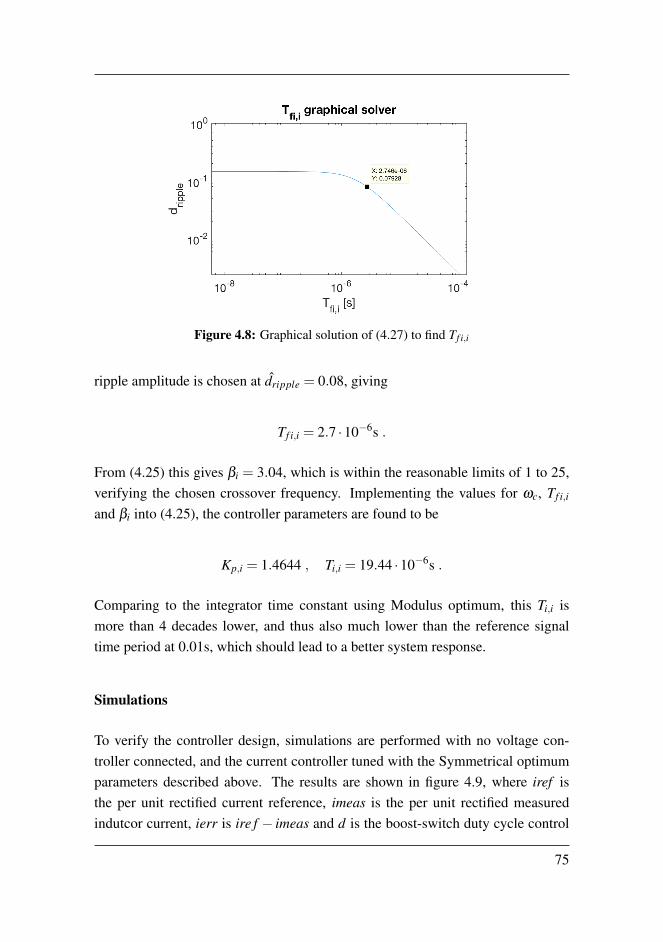
Figure 4.8: Graphical solution of (4.27) to find Tf i,i
ripple amplitude is chosen at dripple = 0.08, giving
Tf i,i = 2.7 ·10−6s .
From (4.25) this gives βi = 3.04, which is within the reasonable limits of 1 to 25,verifying the chosen crossover frequency. Implementing the values for ωc, Tf i,i
and βi into (4.25), the controller parameters are found to be
Kp,i = 1.4644 , Ti,i = 19.44 ·10−6s .
Comparing to the integrator time constant using Modulus optimum, this Ti,i ismore than 4 decades lower, and thus also much lower than the reference signaltime period at 0.01s, which should lead to a better system response.
Simulations
To verify the controller design, simulations are performed with no voltage con-troller connected, and the current controller tuned with the Symmetrical optimumparameters described above. The results are shown in figure 4.9, where iref isthe per unit rectified current reference, imeas is the per unit rectified measuredindutcor current, ierr is ire f − imeas and d is the boost-switch duty cycle control
75
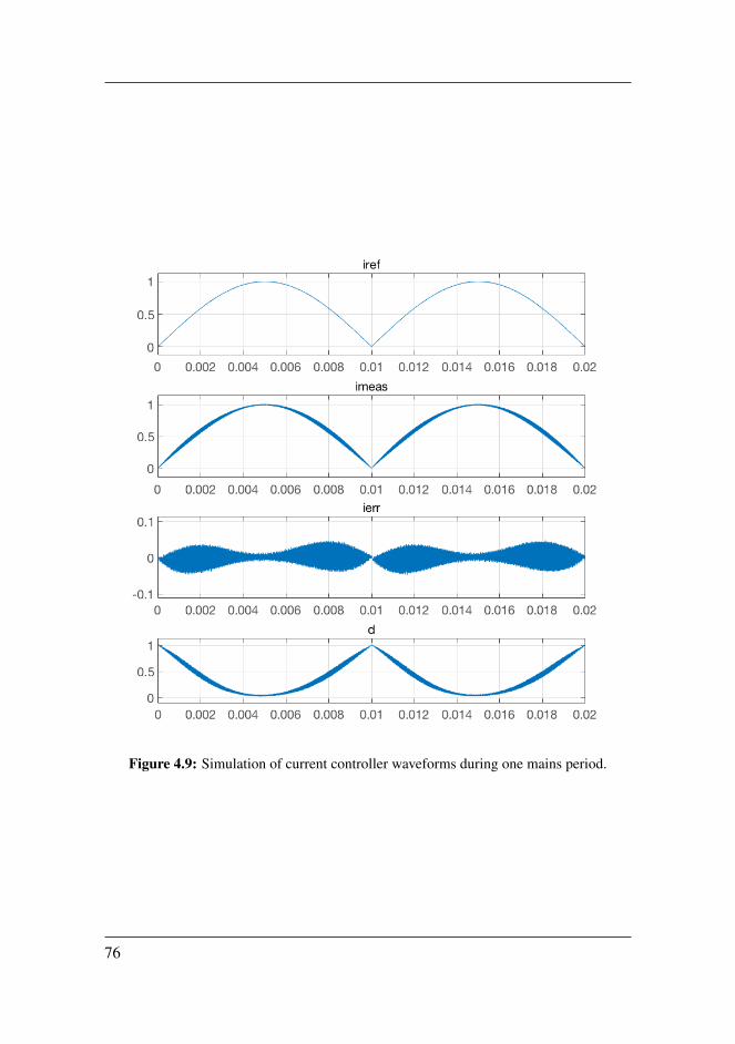
Figure 4.9: Simulation of current controller waveforms during one mains period.
76

signal. These results show that the inductor current following the reference almostperfectly, and the current error consists mostly of the switching-frequency ripple.Looking closely, however, there is a small 100Hz error. This is likely due to somedelay in the PWM stage and the measurement filter, and could be compensated byimplementing e.g. a phase-locked loop (PLL), measuring and controlling the phaseof the current. [50] The PLL will, however, not be pursued further in this master’sthesis, much due to the good phase response of the current loop with symmetricaloptimum, and is left for further work.
77
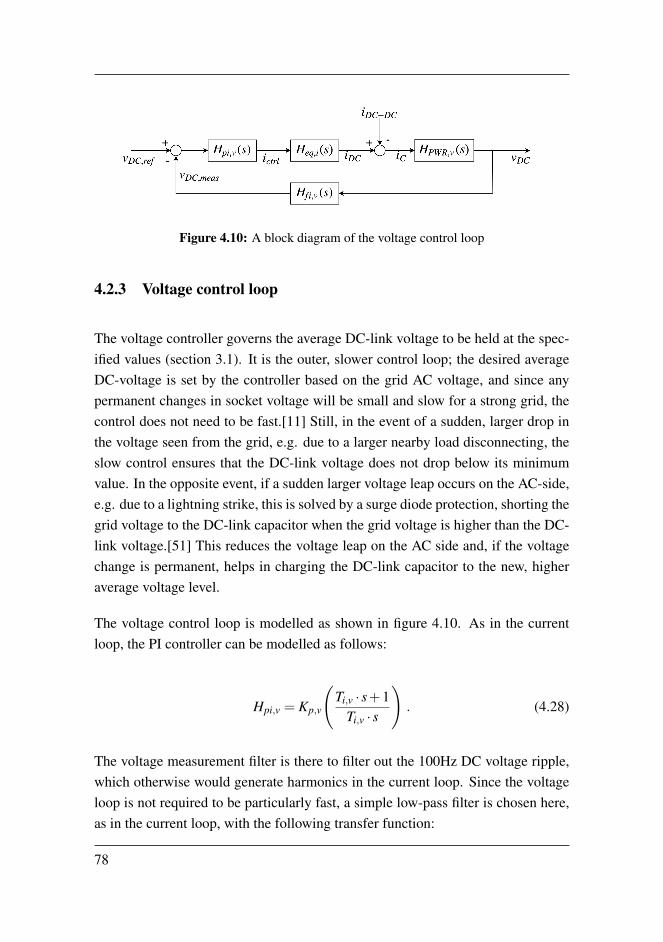
Figure 4.10: A block diagram of the voltage control loop
4.2.3 Voltage control loop
The voltage controller governs the average DC-link voltage to be held at the spec-ified values (section 3.1). It is the outer, slower control loop; the desired averageDC-voltage is set by the controller based on the grid AC voltage, and since anypermanent changes in socket voltage will be small and slow for a strong grid, thecontrol does not need to be fast.[11] Still, in the event of a sudden, larger drop inthe voltage seen from the grid, e.g. due to a larger nearby load disconnecting, theslow control ensures that the DC-link voltage does not drop below its minimumvalue. In the opposite event, if a sudden larger voltage leap occurs on the AC-side,e.g. due to a lightning strike, this is solved by a surge diode protection, shorting thegrid voltage to the DC-link capacitor when the grid voltage is higher than the DC-link voltage.[51] This reduces the voltage leap on the AC side and, if the voltagechange is permanent, helps in charging the DC-link capacitor to the new, higheraverage voltage level.
The voltage control loop is modelled as shown in figure 4.10. As in the currentloop, the PI controller can be modelled as follows:
Hpi,v = Kp,v
(Ti,v · s+1
Ti,v · s
). (4.28)
The voltage measurement filter is there to filter out the 100Hz DC voltage ripple,which otherwise would generate harmonics in the current loop. Since the voltageloop is not required to be particularly fast, a simple low-pass filter is chosen here,as in the current loop, with the following transfer function:
78
H f i,v(s) =1
1+Tf i,i · s. (4.29)
Now to the equivalent current loop transfer function Heq,i(s). To simplify thederivation of controller parameters, it is useful to create an approximate equivalentfirst-order transfer function to the current controller closed-loop transfer function.Assuming that the approximation performed on the second-order voltage-sourceconverter current loop transfer function in [52] is valid for the third order systemin (4.24), the current controller can be approximated as a simple first-order delayTeq,i = 2 ·Tsum,i. The transfer function becomes:
Heq,i(s) =1
1+Teq,i · s=
11+2 ·Tsum,i · s
, (4.30)
where Tsum,i is as before: Tsum,i = TPWM +Tf i,i.
At last, the voltage controller power stage is the DC-link capacitor. The DC-linkvoltage vDC is governed by the DC-link capacitor current iC, which is equal toiC = iDC− iDC−DC, by iC(t) = C · dvDC/dt. The ESR is negligible in the DC-linkcapacitor, thus it can be modelled as a pure capacitance. Using that, the powerstage transfer function can be given as the Laplace form of the capacitor equation:
HPWR,v(s) =vDC(s)iC(s)
=1
C · s. (4.31)
Looking at figure 2.1, it is evident that the only current that we can control is iDC;iDC−DC can be seen as a disturbance and thus be disregarded for the PI controllerdesign later. Combining (4.28)-(4.31) with figure 4.10, the voltage controller open-loop transfer function becomes:
Hol,v(s) = Hpi,v ·Heq,i(s) ·HPWR,v(s) ·H f i,v(s) ,
=Kp,v
Ti,vC· 1+Ti,i · s
s2 · (1+2 ·Tsum,i · s)(1+Tf i,v · s).
(4.32)
As with the current controller, the two minor time constants can be merged into
79

one as Tsum,v = 2 ·Tsum,i +Tf i,v, giving new open-loop transfer function:
Hol,v(s) =Kp,v
Ti,vC· 1+Ti,i · s
s2 · (1+Tsum,v · s). (4.33)
The PI parameters, Kp,v and Ti,v, as well as the filter time constant, Tf i,v, are un-known and need to be tuned. This will be done using the Symmetrical optimum,as explained in the following:
PI tuning: Symmetrical optimum
As shown in (4.33), there is a double free integrator, which by cancelling out (1+Tsum,v · s) by setting Ti,v = Tsum,v using Modulus optimum would result in a phaseof 180, and the system would be on the limit of stability.[49] Thus, Symmetricaloptimum is a better choice for the voltage control loop. The control equationsbecome, similarly as in (4.25):
Ti,v = βv ·Tsum,v , Kp,v =L√
βvTsum,v, ωc,v =
1√βvTsum,v
, (4.34)
In this case, the crossover frequency should be chosen at least half a decade slowerthan the current loop, i.e.: [40]
ωc,v ≤ 10−0.5 ·ωc,i . (4.35)
Moreover, the voltage filter can be designed using the same method as for thecurrent measurement filter in (4.27), this time with equation:
Ictrl,ripple(ωripple) = ωc,vC ·1√
1+(ωrippleTf i,v)2· 1
2∆vC(ωripple) , (4.36)
where Ictrl,ripple is the peak ripple of the output control current from the PI con-troller. As opposed to the current controller, the objective of the voltage mea-surement filter is not to enable a fast response with high crossover frequency, butrather minimizing the 100Hz ictrl,ripple, to minimize harmonics generated in the
80
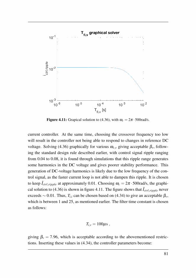
Figure 4.11: Grapical solution to (4.36), with ωc = 2π ·500rad/s.
current controller. At the same time, choosing the crossover frequency too lowwill result in the controller not being able to respond to changes in reference DCvoltage. Solving (4.36) graphically for various ωc,v giving acceptable βv, follow-ing the standard design rule described earlier, with control signal ripple rangingfrom 0.04 to 0.08, it is found through simulations that this ripple range generatessome harmonics in the DC voltage and gives poorer stability performance. Thisgeneration of DC-voltage harmonics is likely due to the low frequency of the con-trol signal, as the faster current loop is not able to dampen this ripple. It is chosento keep Ictrl,ripple at approximately 0.01. Choosing ωc = 2π ·500rad/s, the graphi-cal solution to (4.36) is shown in figure 4.11. The figure shows that Ictrl,ripple neverexceeds ∼ 0.01. Thus, Ti,i can be chosen based on (4.34) to give an acceptable βv,which is between 1 and 25, as mentioned earlier. The filter time constant is chosenas follows:
Ti,v = 100µs ,
giving βv = 7.96, which is acceptable according to the abovementioned restric-tions. Inserting these values in (4.34), the controller parameters become:
81
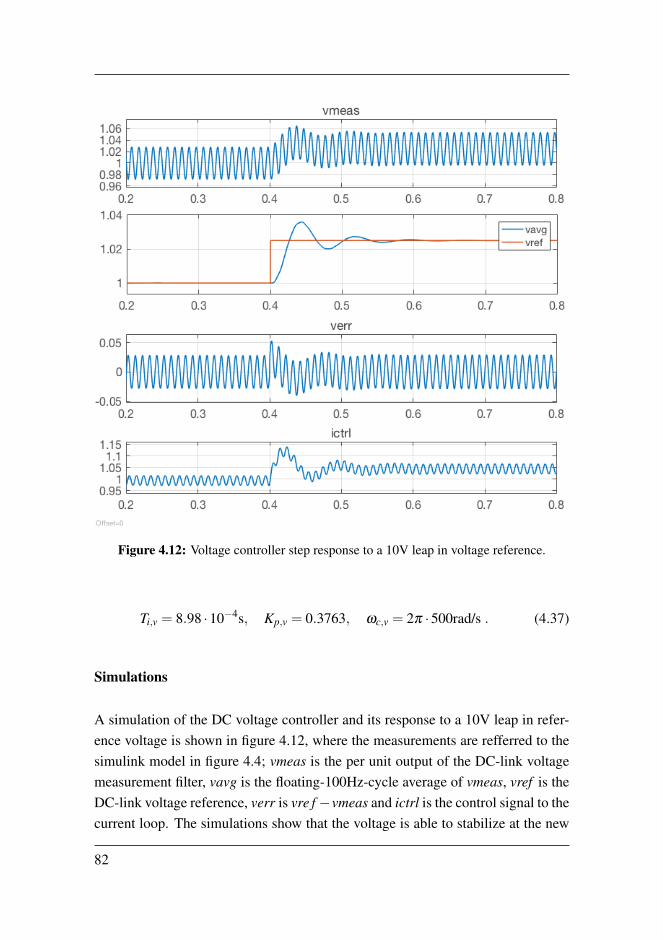
Figure 4.12: Voltage controller step response to a 10V leap in voltage reference.
Ti,v = 8.98 ·10−4s, Kp,v = 0.3763, ωc,v = 2π ·500rad/s . (4.37)
Simulations
A simulation of the DC voltage controller and its response to a 10V leap in refer-ence voltage is shown in figure 4.12, where the measurements are refferred to thesimulink model in figure 4.4; vmeas is the per unit output of the DC-link voltagemeasurement filter, vavg is the floating-100Hz-cycle average of vmeas, vref is theDC-link voltage reference, verr is vre f −vmeas and ictrl is the control signal to thecurrent loop. The simulations show that the voltage is able to stabilize at the new
82
reference within ∼ 0.2s, or roughly 20 100Hz cycles. Moreover, there is a signifi-cant overshoot in the voltage response. However, the leap in DC voltage referencemight be caused by a leap in AC voltage amplitude, in which case an overshootis better than a slower response with no overshoot, since it avoids the AC voltageamplitude being bigger than the DC voltage. This would disturb the boost oper-ation until the AC voltage drops or the DC-link capacitor is charged through thesurge diode and the necessary balance vDC > vAC is re-achieved. A big reason forthe slow response is the size of capacitance, limiting the possible dvDC/dt slope,but another is probably the voltage measurement filter. A faster response couldlikely have been achieved using a higher-order low-pass filter or a band-stop filter,or digital filters such as e.g. a digital low pass filter. [53] All of these enable moreprecise filtering of the ripple frequency, while passing through more of the otherfrequencies, giving faster feedback in the loop. Other smart filtering techniquescould also have been used, such as the voltage measurement filter applied to thesimple PFC in [54], where the ripple is estimated based on current and averagevoltage, and then subtracted from the measured signal, leaving just the averagevoltage. Still, while the more advanced filter variants might give a faster and moreprecise response, figure 4.9 shows that stability is achieved using a low-pass filterwith a good response. Supplementary DC-link voltage control from the DC-DCconverter will normally also be applied, improving the stability even more. [1]
83

84
Chapter 5System-level simulations
To verify the complete proposed converter, some simulations are performed ona system level, for maximum-power G2V and V2G operation at two AC voltagelevels: 230Vrms and 120Vrms. Pictures of the complete system implemented inSimulink can be found in appendix E, except the gate drive logic and control sys-tem, who are depicted in figures 4.1 and 4.4. Components are implemented withthe values computed in sections 3 and 4. There are however no GaN eHEMT mod-els in MATLAB, so thiese are implemented as MOSFETs with no reverse recoverycharge or forward voltage in the body diode, and with the same on-state resis-tance. The MOSFET model used, from the Simscape Power Electronics library inSimulink, does not present any possibility of including the parasitic capacitances,and so the gate charge is assumed infinitely small. Another modification is thatduring V2G the DC-link capacitor is exchanged for a DC voltage source. This isdone to overcome that no DC-DC converter is connected at the DC-side, meaninga power source is necessary to deliver power to the grid. Due to the low rippleof the DC-link voltage at < 20Vp2p, this is approximated here as a DC voltagesource equal to the average DC-link voltage. The simulations are performed witha discrete solver with constant step size 5 ·10−8s.
Results of the simulations at 230Vrms G2V and V2G are shown in figures 5.1 and5.2, respectively. Similar results are found at 120Vrms, and so these simulationresults are attached in appendix G. The results at both voltage levels show that
85
the bidirectional totem-pole PFC is operating properly in both operation modes,with the current following the voltage in G2V and inverting in V2G, while the100Hz DC voltage ripple and the switching-frequency current ripple within thelimits defined in table 1.2. The THD of the AC current is computed in Simulink tobe
T HDi = 0.05 ,
and the power angle, i.e. the phase angle of the fundamental AC current is com-puted as
φi = 2.86 .
That gives power factor: [24, ch. 3-2-4]
p f =1√
1+T HD2i
· cos(φi) = 0.998 .
This power factor will be further improved by the implementation of a filter onthe AC-side decreasing the THD of the AC current drawn from the grid. Then theOBC can comply also with the V2G THD restriction described in table 1.1.
86
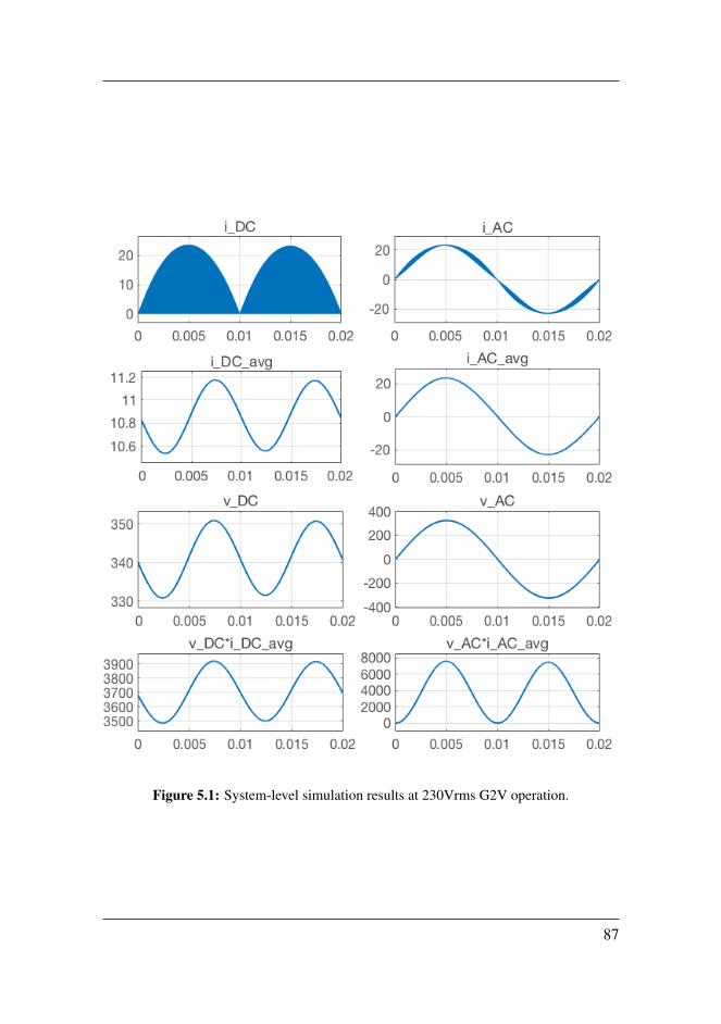
Figure 5.1: System-level simulation results at 230Vrms G2V operation.
87
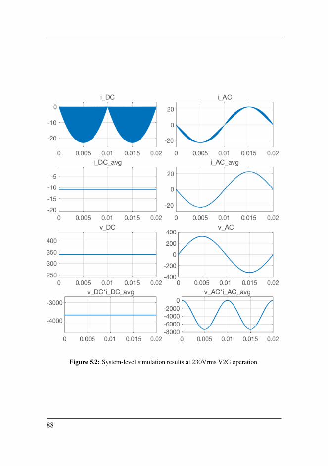
Figure 5.2: System-level simulation results at 230Vrms V2G operation.
88
Chapter 6Feasibility of the bidirectionaltotem-pole PFC
Although the simulations showed that the proposed model is operation properly,the model is a result of some approximations and simplifications who need to betaken into account when evaluating the validity of the results and feasibility ofthe bidirectional totem-pole PFC. Moreover, the performance of the PFC needsto be evaluated in a bigger context, comparing it to the existing solutions on themarket. In the following, the feasibility of the proposed bidirectional totem-polePFC will be discussed, in light of the shortcomings of the simulation model andhow the performance of the totem-pole PFC compares with existing unidirectionalPFC solutions.
6.1 Model shortcomings
The simulation model developed and tested in the previous chapters is, as men-tioned, made to derive and demonstrate the fundamental operation of a bidirec-tional totem-pole PFC. Thus, to limit the scope of work, some effects have beenneglected which might have an effect on the performance of a potential practicalimplementation. For one, no parasitic inductances or capacitances, which wouldinevitably be present in any PCB embodiment of this bidirectional totem-pole PFC,
89

have been included. Though these are mostly too small to affect the fundamentalwaveforms of voltages and currents, e.g. parasitic stray inductances can causeovervoltages over the transistors during switching, when they experience a rapidlydecreasing current, inducing a negative voltage over the inductance.[24, ch. 27-6]
Another point is that the simulations have not been made with proper GaN eHEMTsimulation models, due to the lack of such a model in Simulink. In stead, they havebeen approximated with MOSFETs with no reverse recovery or forward voltagein the diodes, and negligible gate charge. With the infinitely small gate charges,the switching transients of the GaN eHEMTs are not included in the simulations,allowing infinitely fast switching, which is not real. If these transients were in-cluded, they would e.g. lead to some small delays in the system, which couldpotentially affect the stability of the control system.
Moreover, the practical implementation of the gate drives have not been discussed.GaN eHEMTs impose special requirements in the gate drives, since they requirea quite large negative off-state gate voltage to avoid unwanted turn-on, as shownin table 3.3. Besides the fact the gate drive circuit imposes a delay itself, a morecomplex gate drive circuit might increase that delay, also possibly affecting thestability of the controllers.
Furthermore, a parasitic effect which has been proven in regular totem-pole PFCsand has been disregarded here, are current spikes that are discovered to frequentlyoccur at the zero-crossing.[55] These are found to be caused by stored minoritycharges in the slow rectifier diodes, leading the diodes to be forward biased as theAC voltage switches polarity, creating a very big voltage over the inductor, againinducing a big current. Such an issue could be present in the body diodes of therectifier-leg MOSFETs during G2V operation, when they are forward-biased.
Effects such as these and possible other problems related to parasitic effects willhave to be tested in a practical prototype, in order to fully validate the bidirectionaltotem-pole PFC for use in a bidirectional OBC.
90
6.2 Loss comparison to a regular boost PFC
Setting aside the bidirectional conduction ability, which is now proven in the bidi-rectional totem-pole PFC, the proposed solution should be compared to a conven-tional boost PFC with respect to performance. If a bidirectional OBC is to beimplemented, it should be able to compete with existing unidirectional PFC solu-tions, as the primary objective of the bidirectional OBC is still to charge the EVbattery.
To evaluate the efficiency of the proposed bidirectional totem-pole PFC, it is rel-evant comparing the losses to a regular boost PFC. From the analysis so far it isfound that the losses in the DC-link capacitor are insignificant, while rectifyingthe inductor current does not change the RMS and peak currents of the inductorcompared to those found in section 2.3, meaning the losses should be equal. Thus,the key difference in losses exist in the semiconductor devices. First of all, theregular boost has more semiconductors in the conduction path (3) than the totem-pole (2), thus increasing the losses. Another aspect is that diodes and MOSFETsand HEMTs have different conduction loss characteristics; the conduction lossesof MOSFETs and HEMTs have a dependency on I2
S,RMS, as shown in (2.22), whilethe conduction losses of diodes are dependent on ID,avg to the power of one, as-suming negligible diode resistance. The conduction losses of a diode are given asfollows: [24, ch. 20-4]
Pcond,diode =Vf ,diode · Idiode,avg +Ron,diode · I2diode,RMS (6.1)
where Vf ,diode is the diode forward voltage and Ron,diode is the diode on-state resis-tance. The on-state resistance of a diode is usually much smaller than the on-stateresistance of a MOSFET or HEMT. As a consequence, the diode often has lowerconduction losses than the MOSFET and HEMT at high power levels, while it mayhave bigger conduction losses at lower power levels, due to the forward voltage.
In the regular boost PFC this can be utilized by another difference between thetwo topologies, which becomes evident through the transistor current analysis insection 2.4. It is shown in (2.21) and (2.14) that the RMS current through theswitches are dependent only on the AC RMS current. This is due to the symmetryin the totem-pole PFC, where the current has to always pass through either one
91
of the switches in each leg at all times, and the roles are interchanged every halfcycle. This means that to minimize the transistor losses of the bidirectional totem-pole PFC it is beneficial to choose the DC-link voltage as low as possible, as isdone in section 3.1.1. For a regular boost PFC, on the other hand, the roles ofthe transistor and the freewheeling diode do not change every half cycle, meaningthe average and RMS currents through each of these are dependent on the dutycycle, which again is dependent on the DC-link voltage. It can be shown insertingdboost = 1−VAC/VDC into 2.31 that the RMS current through the boost switch in aconventional boost PFC can be expressed as
Iboost =
√I2AC−
83π
VAC
VDCI2AC cos(φAB) . (6.2)
The RMS current through the freewheeling diode, Idiode,RMS is equal to the RMScurrent through the totem-leg complementary switch, described in (2.33), whilethe average current through the diode, Idiode,avg, is equal to the average DC-loadcurrent, which can be expressed as follows:
Idiode,avg =PDC
VDC. (6.3)
The equations (2.33), (6.2) and (6.3) show that the RMS and average currentsthrough the semiconductors in the conventional boost PFC are dependent on theDC-link voltage; the boost transistor current increases with increased DC voltage,while the freewheeling current decreases with increasing DC-voltage. Since it wasestablished earlier that the diode performs better at high power and the transistorperforms better at low power, it will be beneficial during high power power tomaximize Idiode,avg and minimize Iboost by setting VDC at its lowest permitted level.In this application this is defined to be 340V. Oppositely, it will be optimal settinghigh VDC during low power.
In the diode rectifier bridge, there will always be two diodes conducting, and so thelosses Pcond,bridge can be found from (6.1) with Vf ,bridge = 2 ·Vf ,diode, Ron,bridge =
2 ·Ron,diode, Ibridge,avg = IAC,avg (from (2.25)) and Ibridge,RMS = IAC.
92
6.2.1 Comparison at worst-case operating temperature
Since it is assumed in the proposed design that the charger will most often beoperating at maximum power, a quantitative comparison of the conduction lossesin the two topologies is performed at maximum power, at worst-case tempera-ture and with the same GaN HEMT GS66516 as before operating as boost switchin the conventional boost PFC. The operating temperature of the diode bridgeis set at Tcase,bridge = 100C to avoid thermal runaway.[56] As there exist fast-switching diodes, such as Silicon Carbide (SiC) Schottky Barrier diodes, and theDC-link voltage is equal, the switching losses are assumed to be approximatelyequal at approximately the same switching frequency. Assuming Diodes Incorpo-rated GBJ2506 used for the bridge and ROHM Semiconductors SiC Schottky Bar-rier diode SCS220AE used for the freewheeling diode, we have Vf ,bridge = 1.05V,Ron,bridge ≈ 0, Vf ,diode = 1.50V and Ron,diode ≈ 0. Inserting these values alongwith VAC = 230Vrms, VDC,avg = 340 and IAC = 16Arms, the worst-case conduc-tion losses of the conventional boost PFC is found as follows based on (2.22),(6.1),(6.2), (6.3) and (2.33):
Pcond,conv,worst−case = Pcond,bridge +Pcond,diode +Pcond,boost = 34.58W (6.4)
In comparison, the total conduction loss of the proposed totem-pole PFC is equalto the conduction losses of all the transistors, calculated from the worst-case lossesfound in section 3.2, with GS66516 in the totem-leg and IPW60R045CPA in therectifier-leg:
Pcond,totem,worst−case = 2 ·Pcond,ST +2 ·Pcond,SR = 44.80W . (6.5)
The results show that the totem-pole PFC imposes a substantial increase in conduc-tion losses of 30% at the worst-case case temperature and high power, despite thedecreased number of semiconductors. This is due to the different conduction losscurrent dependency of the MOSFETs/eHEMTs and the diodes explained above.A solution to this problem could be to exchange the rectifier-leg MOSFETs forIGBTs connected in anti-parallel with low-forward-voltage diodes. Like diodes,IGBTs are minority carrier devices, with a forward voltage the dominant cause of
93
conduction losses.[24, ch. 25] Thus, the conduction losses current dependency ofthe IGBT is going to be equal to that of the diode, meaning the totem-pole con-duction losses could be reduced by introducing IGBTs anti-paralleled with diodes.That would however imply two more semiconductors in the design, which wouldrequire e.g. a larger heat sink design. One could of course also substitute the samelow-resistance GaN eHEMTs used in the totem-leg, but GaN eHEMTs are moreexpensive than IGBTs and diodes, which are more developed technologies, and soit would likely increase the total cost of the converter.
6.2.2 Comparison at normal operating conditions
Another reason for the higher conduction losses of the totem-pole PFC at worst-case temperature is that the MOSFET and eHEMT on-state resistance has a quitebig positive temperature dependency, while the the forward voltage of the diodeshas a much smaller temperature dependency, as is evident in the data sheets of thechosen semiconductors of this analysis. In other words, the conduction losses ofthe MOSFETs and eHEMTs increase at worst-case temperature, while the conduc-tion losses of the diodes do not change as much. In normal operation, the operatingtemperature will be lower than the worst-case temperature, and thus the losses innormal operation will obviously be different. The operating case temperature willtypically be below 80C, depending on the cooling technique, which would in-duce much smaller losses in the GaN eHEMTs and MOSFETs than at worst-caseTcase = 150C.
A new computation is performed at Tcase = 80C, with corresponding on-stateresistances and forward voltages from the data sheets: RDS,on,HEMT = 37.5mΩ,RDS,on,MOSFET = 60mΩ, Vf ,bridge = 1.05V and Vf ,diode = 1.40V. Substituting thenew resistances into the calculations in section 3.2 and using (6.4) and (6.5) asbefore, the conduction losses during normal operation is computed to be:
Pcond,conv,normal = 33.16W, Pcond,totem,normal = 24.96W .
These calculations show that during normal operation with Tcase = 80C, the bidi-rectional totem-pole PFC decreases the conduction losses by 25% compared to aconventional boost PFC. Moreover, the conduction losses of the totem-pole should
94
decrease more for lower load, due to the I2 dependency, than the conventional PFC.Thus, although the switching losses are not taken into account and the loss com-putations might not be completely precise due to inaccuracies in the data sheets,these computations indicate that the proposed bidirectional totem-pole imposes animprovement in efficiency compared to conventional boost PFC at 230Vrms andnormal operation.
6.2.3 Comparison at 120Vrms
Having established that the totem-pole PFC is efficient at 230Vrms, a similar com-parison must be made at 120Vrms to evaluate over its full voltage range. In fact, asmentioned in section 3.2, a significant disadvantage of the totem-pole PFC emergesat lower voltage levels; while the power decreases to almost half when the AC volt-age is changed from 230Vrms to 120Vrms, the switching losses and conductionlosses of the bidirectional totem-pole PFC are unaffected by the AC voltage - onlythe AC current and DC voltage. This means the relative losses are almost doubledat 120Vrms, causing a big decrease in efficiency. Looking at (6.2) and (6.3) itis evident that the conduction losses of the conventional PFC are indeed depen-dent on the AC voltage and power. As it turns out, when the AC voltage - andpower - decreases, the current through the boost switch of the conventional PFCincreases while the current through the freewheling diode decreases. Based on theprevious analysis of the current dependency of the conduction losses of diodes andMOSFET and HEMTs, this should mean an increase in conduction losses in theconventional PFC at 120Vrms, implying even worse efficiency.
The conduction losses of the conventional PFC at 120Vrms and worst-case oper-ating conditions can be calculated as follows, using the same procedure as in theprevious analyses:
Pcond,conv,120V = 39.82W ,
which, as expected, is an increase of 15% compared to the worst-case analysisat 230Vrms. Assuming all the other losses computed in chapter 3 to remain un-changed, and keeping in mind that these were designed to give more or less exactly98% efficiency at 230Vrms and 3500kW, it is obvious that the efficiencies of both
95
the conventional boost PFC and the bidirectional totem-pole PFC at 120Vrms and1.9kW will be less than 98%.
Since the PFC should be able to operate with 98% efficiency at both 120Vrms and230Vrms, and the efficiency of this bidirectional totem-pole PFC is closer to 96%at 120Vrms normal conditions, some modifications should be made to increase theefficiency at low voltage. An example of such a modification could be connectingextra totem-leg GaN eHEMTs or rectifier-leg MOSFETs in parallel; a halving ofthe current through each of these transistors implies a 4-times decrease in conduc-tion losses in each transistor, by (2.22), thus halving the conduction losses. MOS-FETs and GaN HEMTs can safely be connected in parallel because of the positivetemperature coefficient of the on-state resistances ensuring an even loss distribu-tion between the paralleled transistors. There are however some challenges whenconnecting transistors in parallel, such as e.g. equalling the impedance of the gatecircuits of both of the paralleled transistors to ensure simultaneous switching. Onthe other hand, it has been shown in [29] that interleaving the totem legs can givepositive effects with regards to current ripple, cancelling out harmonics, mean-ing there are more positive effects to connecting in parallel as well. In any case,paralleling the transistors would indeed give a more complex system, making itdesireable to avoid if possible. Thus another solution to this problem could be todecrease and redistribute the estimated losses in table 3.2, to e.g. have approx-imately the same totem-leg losses, while restricting especially the inductor andrectifier leg allowed losses. The inductor conduction losses could be decreased byincreasing the core size, and the rectifier legs have no switching losses and couldthus be made with smaller losses than the totem-leg. However, the first would de-crease the power density, whereas the second would likely require more expensivetransistors.
96
Chapter 7Conclusion and Further Work
7.1 Conclusion
A fundamental simulation model of a bidirectional totem-pole PFC for bidirec-tional OBC purposes has been built and implemented in Simulink using off-the-shelf components while complying with the demands put forward by Valeo Siemens.General equations have been developed for the description of currents, voltagesand losses in the components throughout the topology, aiding in the dimension-ing of these components. Importantly, it was discovered that the transistor con-duction losses in the bidirectional totem-pole are only dependent on the AC cur-rent, because of the symmetry of the topology forcing the conduction losses tobe equally distributed across both transistors in each leg. The components im-plemented were a 246µH powder-core, toroid-shaped boost inductor with copperwires, 5 paralleled 360µF electrolytic DC-link capacitors, GaN eHEMT GS66516for high-frequency transistors and CoolMOS IPW60R045CPA for slow-switchingrectifier-leg transistors. Combined, they were computed to give an efficiency ofmore than 98% at a switching frequency of 90kHz.
Moreover, equations for gate logic and control system with cascaded current andvoltage control have been developed and implemented in Simulink, and verifiedthrough simulations. The current and voltage controllers were implemented withPI controllers and Symmetrical optimum, giving crossover frequencies of 28kHz
97
and 500Hz, respectively, with good response. The simulations showed that thecharger was able to operate at 120Vrms and 230Vrms max power with a powerfactor of 0.998 and a THD of 5% without any DM filter applied on the AC side.This was not complying with the AC current THD limitations at 3% in V2G, andthus a DM filter will have to be applied in order to meet these demands.
At last the performance of the proposed bidirectional totem-pole was compared toa conventional boost PFC at worst-case and normal operating modes at 230Vrms,and at 120Vrms. This analysis showed that the bidirectional totem-pole PFC pro-duced higher conduction losses than the conventional boost PFC at worst-case op-erating conditions with case temperature 150C. This was concluded to be becausethe conduction losses of the eHEMTs and MOSFETs being dependent on the cur-rent squared while for the freewheeling diode of the conventional boost they aredependent on the current to the power of one, combined with the fact that theconduction losses of the conventional PFC can be regulated by adjusting the DC-link voltage to direct more of the current through the diode and less through theboost MOSFET. However, it was shown that during normal operation, the strongtemperature dependency of the MOSFET and GaN HEMT on-state resistancesdecreased the conduction losses to make the bidirectional totem-pole PFC moreefficient than the conventional boost PFC. Still, it was shown at 120Vrms that theconduction loss - and switching loss - independence from AC voltage of the bidi-rectional totem-pole PFC causes the efficiency to decrease significantly at lowervoltages, approaching 96% at 120Vrms. This effect is however found to be evenworse in conventional PFCs.
All in all, the bidirectional totem-pole seems a promising topology for use asa bidirectional PFC, being feasible with existing off-the-shelf components, andshowing good control performance in both G2V and V2G operation. It was ar-gued in the introduction that the charger would most often be operating at maxpower in both G2V and V2G, and at 230Vrms max power the performing at agood efficiency η > 98%. Moreover, at 230Vrms lower power, the totem-pole isexpected to show even better performance, due to the mentioned I2-dependency ofthe conduction losses in the transistors. However, at 120Vrms, the efficiency wasfound to not meet the demands, and so modifications would need to be made, suchas connecting the high-frequency legs in parallel, in order to achieve a satisfactoryefficiency at lower AC voltages. Also, importantly, the results of this simulation
98
model are not sufficient to verify completely the bidirectional totem-pole, as someparasitic effects and transients are ignored. A real-life prototype will have to bemade to investigate the performance further.
7.2 Further Work
Picking up on that loose thread, the first suggestion for further work is to build aprototype of this bidirectional totem-pole PFC for OBC purposes, with the rele-vant components and with proper gate drive circuits. This way, the real-life per-formance of the 3.5kW bidirectional can be investigated, studying the effect ofthe transient behaviour of the GaN HEMTs and the gate drive circuits on the con-trol system and the rest of the performance. It would also allow for investigationof the effect of PCB parasitics on e.g. overvoltages across the transistors duringswitching; at this high frequency of 90kHz it is desirable to avoid snubber cir-cuits at the transistors, since they impose a delay in the switching, and for thatreason it would be valuable to investigate any overvoltages or too high di/dt anddv/dt during switching, to evaluate the feasibility of the topology. Another tran-sient effect of importance, is the previously mentioned current spike that is shownto occur at zero crossing is with unidirectional PFCs, due to rectifier diodes mi-nority charges.[55] It could be interesting to see if the same effect is present withthe body diodes of the rectifier-leg MOSFETs during G2V, or if implementing abidirectional totem-pole removes this problem.
Withal, a suggestion for further work is investigating further the paralleling of GaNHEMTs in the fast-switching totem-leg, to increase the efficiency of the totem-pole at lower voltages. As mentioned this imposes stringent requirements to thegate drivers with regards to equality of gate impedance, and other issues will bepresent too. Also, interleaving of the totem-pole fast-switching leg with CrCM andTCM has been investigated in several papers in the literature,[29, 27] but few haveinvestigated this interleaving in CCM.
At last, an obvious suggestion for further work is the study of a bidirectional DC-DC converter, to complete the bidirectional OBC. This will in fact be done in amaster’s thesis at NTNU next spring, also in cooperation with Valeo Siemens.
99

100
Bibliography
[1] Internal Valeo Siemens eAutomotive data.
[2] PFC boost converter design guide. URL:https://www.infineon.com/dgdl/Infineon-ApplicationNote PFCCCMBoostConverterDesignGuide-AN-v02 00-EN.pdf?fileId=5546d4624a56eed8014a62c75a923b05, 2013.
[3] Christoph Marxgut, Florian Krismer, Dominik Bortis, and Johann W. Ko-lar. Ultraflat Interleaved Triangular Current Mode (TCM) Single-Phase PFCRectifier. IEEE Transactions on Power Electronics, 29(2):873–882, feb 2014.
[4] Sondre Westby Johannessen. Power factor correction for a bidirectional on-board charger for electric vehicles and plug-in hybrid electric vehicles - spe-cialization project. Technical report, NTNU, 2017.
[5] U.S. Department of Energy. What is the Smart Grid? URL:https://www.smartgrid.gov/the smart grid/smart grid.html, June 2018.
[6] Arne Venjum and Guro Grøtterud. AMS.https://www.nve.no/elmarkedstilsynet-marked-og-monopol/sluttbrukermarkedet/ams/, May 2017.
[7] European Comission Joint Research Centre. Smart Metering deployment inthe European Union. http://ses.jrc.ec.europa.eu/smart-metering-deployment-european-union, December 2017.
[8] William Steel. Encouraging Potential for
101

Self-consumption of Solar PV in Germany.http://www.renewableenergyworld.com/articles/2016/11/encouraging-potential-for-self-consumption-of-solar-pv-in-germany.html, November2016.
[9] Jane Pulaski. IREC Releases New Report: 12,000 MW of Distributed Gener-ation by 2020 – ambitious goal for CA. http://www.irecusa.org/2012/07/irec-releases-new-report-12000-mw-of-distributed-generation-by-2020-in-ca/,July 2012.
[10] Becca Jones-Albertus. Confronting the Duck Curve:How to Address Over-Generation of Solar Energy.https://www.energy.gov/eere/articles/confronting-duck-curve-how-address-over-generation-solar-energy, October 2017.
[11] Jan Machowski, Janusz W. Bialek, and James R. Bumby. Power SystemDynamics - Stability and Control. John Wiley & Sons, Ltd., second edition,2012.
[12] Battery University. BU-808b: What Causes Li-ion to Die?http://batteryuniversity.com/learn/article/bu 808b what causes li ion to die,August 2014.
[13] J. Vetter, P. Novak, M.R. Wagner, C. Veit, K.-C. Moller, J.O. Besenhard,M. Winter, M. Wohlfahrt-Mehrens, C. Vogler, and A. Hammouche. Age-ing mechanisms in lithium-ion batteries. Journal of Power Sources, 147(1-2):269–281, sep 2005.
[14] Marius Valle. Elbileiere tjener penger pa a være koblet til lader.https://www.tu.no/artikler/elbileiere-tjener-penger-pa-a-vaere-koblet-til-lader/403818, August 2017.
[15] The Parker Project website. http://parker-project.com/.
[16] Mahbubul Alam. Vehicle-to-everything (v2x) technology will be a literal lifesaver – but what is it? http://eecatalog.com/automotive/2016/05/19/vehicle-to-everything-v2x-technology-will-be-a-literal-life-saver-but-what-is-it/,May 2016.
102
[17] Narain G. Hingorani and Laszlo Gyugyi. Understanding FACTS. IEEE Press,2000.
[18] Charles Morris. Mitsubishi Outlander PHEV adds vehicle-to-home powerexport capability. https://chargedevs.com/newswire/mitsubishi-outlander-phev-adds-vehicle-to-home-power-export-capability/, December 2014.
[19] Anthony Rico. Power When Away From Home — Using a Power In-verter. https://www.batterystuff.com/blog/using-a-power-inverter.html, De-cember 2016.
[20] World Standards. Plug, socket & voltage by country. URL:https://www.worldstandards.eu/electricity/plug-voltage-by-country/, April2018.
[21] Murat Yilmaz and Philip T. Krein. Review of Battery Charger Topologies,Charging Power Levels, and Infrastructure for Plug-In Electric and HybridVehicles. IEEE Transactions on Power Electronics, 28(5):2151–2169, may2013.
[22] Tanja Mesek. Are you on-board? Demystifying EV charging sys-tems. https://e2e.ti.com/blogs /b/powerhouse/archive/2017/07/31/are-you-on-board-demystifying-ev-charging-systems, July 2017.
[23] J. Kolar, J. Biela, and J. Minibock. Exploring the pareto front of multi-objective single-phase PFC rectifier design optimization - 99.2% efficiencyvs. 7kW/din3 power density. In 2009 IEEE 6th International Power Elec-tronics and Motion Control Conference, pages 1–21. IEEE, may 2009.
[24] Ned Mohan, Tore M. Undeland, and William P. Robbins. Power Electronics -Converters Applications and Design. John Wiley & Sons, inc., third edition,2003.
[25] L. Huber, Yungtaek Jang, and M.M. Jovanovic. Performance Evaluation ofBridgeless PFC Boost Rectifiers. IEEE Transactions on Power Electronics,23(3):1381–1390, may 2008.
[26] Ken K.M. Siu and Carl N.M. Ho. A critical review of Bridgeless PFC boostrectifiers with common-mode voltage mitigation. In IECON 2016 - 42nd
103
Annual Conference of the IEEE Industrial Electronics Society, pages 3654–3659. IEEE, oct 2016.
[27] Zhengyang Liu, Fred C. Lee, Qiang Li, and Yuchen Yang. Design of GaN-based MHz totem-pole PFC rectifier. In 2015 IEEE Energy ConversionCongress and Exposition (ECCE), pages 682–688. IEEE, sep 2015.
[28] Laszlo Huber, Brian T. Irving, and Milan M. Jovanovic. Effect of ValleySwitching and Switching-Frequency Limitation on Line-Current Distortionsof DCM/CCM Boundary Boost PFC Converters. IEEE Transactions onPower Electronics, 24(2):339–347, feb 2009.
[29] C. Marxgut, J. Biela, and J. W. Kolar. Interleaved Triangular Current Mode(TCM) resonant transition, single phase PFC rectifier with high efficiencyand high power density. In The 2010 International Power Electronics Con-ference - ECCE ASIA -, pages 1725–1732. IEEE, jun 2010.
[30] GaN Systems. High Efficiency CCM Bridgeless Totem Pole PFC Designusing GaN E-HEMT Reference Design. www.gansystems.com.
[31] Minho Kwon and Sewan Choi. An Electrolytic Capacitorless BidirectionalEV Charger for V2G and V2H Applications. IEEE Transactions on PowerElectronics, 32(9):6792–6799, sep 2017.
[32] Jih-Sheng Lai, Lanhua Zhang, Zaka Zahid, Nan-Hsiung Tseng, Chi-SengLee, and Chin-Hone Lin. A high-efficiency 3.3-kW bidirectional on-boardcharger. In 2015 IEEE 2nd International Future Energy Electronics Confer-ence (IFEEC), pages 1–5. IEEE, nov 2015.
[33] Stefan Endres, Christoph Sessler, Stefan Zeltner, Bernd Eckardt, and TatsuoMorita. 6 kW Bidirectional, Insulated On-board Charger With Normally-offGaN Gate Injection Transistors. In PCIM Europe, pages 573–578, Nurem-berg, Germany, 2017.
[34] Liang Zhou, Yi Feng Wu, and Umesh Mishra. True-bridgeless totem-polePFC based on GaN HEMTs. pages 1017–1022. Mesago PCIM GmbH, 2013.
[35] Zhengyang Liu, Bin Li, Fred C. Lee, and Qiang Li. High-Efficiency High-Density Critical Mode Rectifier/Inverter for WBG-Device-Based On-Board
104
Charger. IEEE Transactions on Industrial Electronics, 64(11):9114–9123,nov 2017.
[36] Xiucheng Huang, Qiang Li, Zhengyang Liu, and Fred C. Lee. AnalyticalLoss Model of High Voltage GaN HEMT in Cascode Configuration. IEEETransactions on Power Electronics, 29(5):2208–2219, 5 2014.
[37] Kemet Electronic Components. Capacitor Basic Principles, 2016.
[38] F. Roccaforte, P. Fiorenza, G. Greco, M. Vivona, R. Lo Nigro, F. Giannazzo,A. Patti, and M. Saggio. Recent advances on dielectrics technology for SiCand GaN power devices. Applied Surface Science, 301:9–18, may 2014.
[39] Emre Gurpinar and Alberto Castellazzi. Single-Phase T-Type Inverter Perfor-mance Benchmark Using Si IGBTs, SiC MOSFETs and GaN HEMTs. IEEETransactions on Power Electronics, pages 1–1, 2015.
[40] Roy Nilsen. Compendium TET4120 Electric Drives, April 2018.
[41] Shamim Choudhury. Average Current Mode Controlled Power Factor Cor-rection Converter using TMS320LF2407A. 2005.
[42] J. Rajagopalan, F.C. Lee, and P. Nora. A general technique for derivation ofaverage current mode control laws for single-phase power-factor-correctioncircuits without input voltage sensing. IEEE Transactions on Power Elec-tronics, 14(4):663–672, jul 1999.
[43] Chen Zhou and Milan M Jovanovic. Design trade-offs in continuous current-mode controlled boost power- factor correction circuits. In High FrequencyPower Conversion Conference (HFPC ’92), Seventh Internationa, 1992.
[44] J.W. Umland and M. Safiuddin. Magnitude and symmetric optimum criterionfor the design of linear control systems: what is it and how does it comparewith the others? IEEE Transactions on Industry Applications, 26(3):489–497, 1990.
[45] Zheren Lai and K.M. Smedley. A family of continuous-conduction-modepower-factor-correction controllers based on the general pulse-width modu-lator. IEEE Transactions on Power Electronics, 13(3):501–510, may 1998.
[46] Woo-Young Choi, Jung-Min Kwon, Eung-Ho Kim, Jong-Jae Lee, and Bong-
105
Hwan Kwon. Bridgeless Boost Rectifier With Low Conduction Losses andReduced Diode Reverse-Recovery Problems. IEEE Transactions on Indus-trial Electronics, 54(2):769–780, apr 2007.
[47] Martin F. Schlecht. Time-varying feedback gains for power circuits withactive waveshaping. In 1981 IEEE Power Electronics Specialists Conference,pages 52–59. IEEE, jun 1981.
[48] J.P. Gegner and C.Q. Lee. Linear peak current mode control: a simple activepower factor correction control technique for continuous conduction mode.In PESC Record. 27th Annual IEEE Power Electronics Specialists Confer-ence, volume 1, pages 196–202. IEEE, 1996.
[49] Jens G. Balchen, Trond Andresen, and Bjarne A. Foss. Reguleringsteknikk.NTNU, January 2003.
[50] M. Ciobotaru, R. Teodorescu, and F. Blaabjerg. A New Single-Phase PLLStructure Based on Second Order Generalized Integrator. In 37th IEEEPower Electronics Specialists Conference, pages 1–6. IEEE.
[51] ON Semiconductors. Transient Overvoltage Protection. URL:https://www.onsemi.com/pub/Collateral/TND335-D.PDF, 2008.
[52] Santiago Sanchez, Gilbert Bergna, and Elisabetta Tedeschi. Tuning of Con-trol Loops for Grid-Connected Modular Multilevel Converters under a Sim-plified Port Representation for Large System Studies. 2017.
[53] D. Tufts and J. Francis. Designing digital low-pass filters–Comparison ofsome methods and criteria. IEEE Transactions on Audio and Electroacous-tics, 18(4):487–494, dec 1970.
[54] Ashish Pandey, Bhim Singh, and Dwarka P Kothari. A SimpleFast Voltage Controller for Single-Phase PFC Converters. URL:https://pdfs.semanticscholar.org/e055/075891d1144699c297a7b12492261485ec91.pdf.
[55] Bin Su, Junming Zhang, and Zhengyu Lu. Totem-Pole Boost Bridgeless PFCRectifier With Simple Zero-Current Detection and Full-Range ZVS Operat-ing at the Boundary of DCM/CCM. IEEE Transactions on Power Electron-ics, 26(2):427–435, feb 2011.
[56] Roger Paul Stout. AND8223, 2006.
106
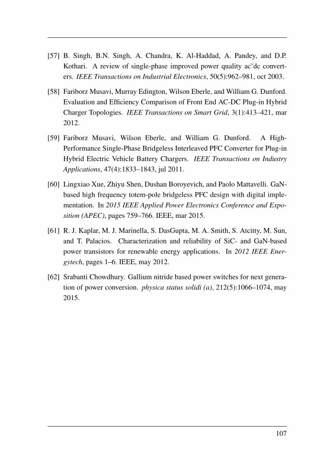
[57] B. Singh, B.N. Singh, A. Chandra, K. Al-Haddad, A. Pandey, and D.P.Kothari. A review of single-phase improved power quality ac˜dc convert-ers. IEEE Transactions on Industrial Electronics, 50(5):962–981, oct 2003.
[58] Fariborz Musavi, Murray Edington, Wilson Eberle, and William G. Dunford.Evaluation and Efficiency Comparison of Front End AC-DC Plug-in HybridCharger Topologies. IEEE Transactions on Smart Grid, 3(1):413–421, mar2012.
[59] Fariborz Musavi, Wilson Eberle, and William G. Dunford. A High-Performance Single-Phase Bridgeless Interleaved PFC Converter for Plug-inHybrid Electric Vehicle Battery Chargers. IEEE Transactions on IndustryApplications, 47(4):1833–1843, jul 2011.
[60] Lingxiao Xue, Zhiyu Shen, Dushan Boroyevich, and Paolo Mattavelli. GaN-based high frequency totem-pole bridgeless PFC design with digital imple-mentation. In 2015 IEEE Applied Power Electronics Conference and Expo-sition (APEC), pages 759–766. IEEE, mar 2015.
[61] R. J. Kaplar, M. J. Marinella, S. DasGupta, M. A. Smith, S. Atcitty, M. Sun,and T. Palacios. Characterization and reliability of SiC- and GaN-basedpower transistors for renewable energy applications. In 2012 IEEE Ener-gytech, pages 1–6. IEEE, may 2012.
[62] Srabanti Chowdhury. Gallium nitride based power switches for next genera-tion of power conversion. physica status solidi (a), 212(5):1066–1074, may2015.
107

108

Appendices
109


Appendix AValeo Siemens bidirectional OBCspecifications
111

NTNU master project Doc. Ref.:
Doc. Rev.: 01
Bidirectional charger Release Date: -
Doc. Classif.: Not restricted
Customer: P3 Product Line: OBC Project Type:
Division: Hardware Platform: - Product: - Project Manager:
Dev./Prod Site(s): Drammen Project Code: - Product Ref.: - Activity Leader: T. Sorsdahl
This document is property of Valeo. No copy or distribution allowed without authorization.
p 1/8
Template Ref: V01 TPL 07 00645 Template Rev: 01
Schematic and layout review and justification.
SKILL PROJECT NAME PLM
Hardware Bidirectional charger
ABSTRACT / CONCLUSION
ABSTRACT:
General specification && guidelines for design of a bidirectional on board charger for electrical and hybrid vehicles intended as a starting point / reference for a master project at NTNU.
The bidirectional charger should be designed for J1772/IEC 61851 which describes the charging standard for electrical vehicles up to level two charging with single phase current up to 32Arms/7680VA. Relevant and extended requirements are specified in this document.
There is no known standardization for bidirectional chargers at the time of creation of this document.
CIRCULATION LIST (E : E-mail, P : Paper)
Can be released Communicable with non disclosure commitment Available on site only Confidential - unavailable
C Name Service or Company C Name Service or Company C
E E E
S YES NO
R YES NO

NTNU master project Doc. Ref.:
Doc. Rev.: 01
Bidirectional charger Release Date: -
Doc. Classif.: Not restricted
Customer: P3 Product Line: OBC Project Type:
Division: Hardware Platform: - Product: - Project Manager:
Dev./Prod Site(s): Drammen Project Code: - Product Ref.: - Activity Leader: T. Sorsdahl
This document is property of Valeo. No copy or distribution allowed without authorization.
p 2/8
Template Ref: V01 TPL 07 00645 Template Rev: 01
Written by Reviewed by Checked by Approved by
Function Hardware Engineer Referent Engineer HDL Department Manager
Name Torbjørn Sørsdahl
Date
Visa
See Signature Workflow Instruction

NTNU master project Doc. Ref.:
Doc. Rev.: 01
Bidirectional charger Release Date: -
Doc. Classif.: Not restricted
Customer: P3 Product Line: OBC Project Type:
Division: Hardware Platform: - Product: - Project Manager:
Dev./Prod Site(s): Drammen Project Code: - Product Ref.: - Activity Leader: T. Sorsdahl
This document is property of Valeo. No copy or distribution allowed without authorization.
p 3/8
Template Ref: V01 TPL 07 00645 Template Rev: 01
SUMMARY
CIRCULATION LIST (E : E-MAIL, P : PAPER).................................................................................................. 1
SUMMARY ................................................................................................................................................................. 3
REVISION HISTORY ................................................................................................................................................ 3
1 GLOBAL REQUIREMENTS................................................................................................................. 4
1.1 GENERAL REQUIREMENTS .......................................................................................................................... 4
1.2 SPECIFICATION G2V ................................................................................................................................... 4
1.3 SPECIFICATION V2G ................................................................................................................................... 4
1.4 EMC REQUIREMENTS ................................................................................................................................. 5
2 INTERNAL OBC REQUIREMENTS ................................................................................................... 6
2.1 PFC STAGE OR SIMILAR TOWARD AC GRID ................................................................................................. 6
2.2 DC/DC OR SIMILAR TOWARD BATTERY ....................................................................................................... 7
3 TIPS / FAST CALCULATIONS AS INPUT ......................................................................................... 8
REVISION HISTORY
Revision # Date Modif # Author Modified paragraphs and kind of modification
1 13.12.2017 1 T.Sorsdahl Initial revision

NTNU master project Doc. Ref.:
Doc. Rev.: 01
Bidirectional charger Release Date: -
Doc. Classif.: Not restricted
Customer: P3 Product Line: OBC Project Type:
Division: Hardware Platform: - Product: - Project Manager:
Dev./Prod Site(s): Drammen Project Code: - Product Ref.: - Activity Leader: T. Sorsdahl
This document is property of Valeo. No copy or distribution allowed without authorization.
p 4/8
Template Ref: V01 TPL 07 00645 Template Rev: 01
1 Global requirements
Rough expectations for performance required for bidirectional on board chargers from standards and other input.
1.1 General requirements
Id Req Description Range
1.1 Galvanic isolation between input and output (transformer) 4kVac
1.2 Encapsulation IP67
1.3 Cooling system by liquid with coolant temperature -40 ~ 85ºC
1.4 Ambient air temperature range -40 ~ 85ºC
1.5 The charger shall meet the following lifetime (service life): 15 years 300 000 km ~ 20.000 hours total V2G && G2V
1.2 Specification G2V
Id Req Description Range
2.1 AC-DC Output voltage range 200 ~ 1000Vdc
2.2. AC-DC Max output current(continuous) 12Adc
2.3 AC-DC Output current ripple 5%
2.4 AC-DC Maximum output power 3500W
2.5 AC-DC Input voltage range 85 ~ 264VAC,rms
2.6 AC-DC Input frequency 45 ~ 65Hz
2.7 AC-DC Maximum input current 16A Max.
2.8 AC-DC Efficiency > 94%.
2.9 AC-DC Max apparent power 3680VA
2.10 AC-DC Lifetime
10.000 hours (Eq 300.000 km)
2.11 Maximum AC leakage current 1.5mA
1.3 Specification V2G
Id Req Description Range
3.1 DC-AC Output voltage range 85-264Vac
3.2 DC-AC Input voltage range 200VDC~1000VDC
3.3 DC-AC Max power output 3.5kW
3.4 DC-AC Max input current 12Adc Max.
3.5 DC-AC Max output current(rms) 16A Max.
3.6 DC-AC output frequency range 45~65Hz
3.7 DC-AC efficiency > 94%.
3.8 DC-AC THD THD<3%
3.9 DC-AC Lifetime
10.000 hours (high uncertainty of required lifetime)
3.10 Maximum AC leakage current 1.5mA

NTNU master project Doc. Ref.:
Doc. Rev.: 01
Bidirectional charger Release Date: -
Doc. Classif.: Not restricted
Customer: P3 Product Line: OBC Project Type:
Division: Hardware Platform: - Product: - Project Manager:
Dev./Prod Site(s): Drammen Project Code: - Product Ref.: - Activity Leader: T. Sorsdahl
This document is property of Valeo. No copy or distribution allowed without authorization.
p 5/8
Template Ref: V01 TPL 07 00645 Template Rev: 01
1.4 EMC requirements
Electric vehicle minimum emc requirements for EU : R010r6e (available for free) done at Vehicle level. This specifies all emc requirements which in the end the charger also need to be according to however component level requirements are usually stricter.
Id Req Description Standard
4.13 Maximum harmonics 50Hz – 2kHz
R010r6e :
IEC 61000-3-2
4.22
Supply voltage dips
Minimum requirement: Voltage reduction of 30 % of nominal voltage for 10 ms.
Minimum requirement: Voltage reduction of 50 % of nominal voltage for 100 ms.
Minimum requirement: voltage reduction >95 % of nominal voltage for 5 s.
No loss of charging state allowed reduced power acceptable IEC 61000-4-11
4.32 1,2/50 μs surges
6kV in common mode,
3 kV in differential mode IEC 61000-4-5
4.42 Conducted emission toward ac grid 150kHz-30MHz
IEC 61000-4-6
4.51 Radiated emission 30MHz-6GHz R010r6e
4.6 Conducted emission toward battery 150kHz-30MHz
R010r6e 1: Outside any scope for a student task 2: For minor reference regarding switching frequency 3: Why a pfc is required.

NTNU master project Doc. Ref.:
Doc. Rev.: 01
Bidirectional charger Release Date: -
Doc. Classif.: Not restricted
Customer: P3 Product Line: OBC Project Type:
Division: Hardware Platform: - Product: - Project Manager:
Dev./Prod Site(s): Drammen Project Code: - Product Ref.: - Activity Leader: T. Sorsdahl
This document is property of Valeo. No copy or distribution allowed without authorization.
p 6/8
Template Ref: V01 TPL 07 00645 Template Rev: 01
2 Internal obc requirements Describes recommendations to be able to the global on board charger requirements.
2.1 PFC stage or similar toward ac grid
Id Req Description Value Reason
PFC startup time to Full operation V2G
<1s
Grid stabilization is usually in the range of seconds
It is assumed the dc/dc is running in idle mode while awaiting feedback from the grid to only need to start the PFC and not charge the dc link in addition which is time consuming.
PFC efficiency >97.6%
Total effiency required 94% estimate loss split : o 40% PFC Min effiency PFC : 97.6% o 40% DC/DC Min effiency dc/dc : 97.6% o 20% Other losses Min effiency required :
98.8% o Sum 94% efficiency.
Hard to meet at 85Vrms due to the losses in the PFC can only be 37% of the value at 230V usually requring much higher rated component at a higher cost.
PFC choke current ripple < 20%
Core losses for most relevant magnetic materials increases by the square of the flux density ripple so 100% ripple increases core losses by 25x compared to 20%.
This limits the maximum current ripple which has to flow in filter capacitors reducing the requirement for current capability.
Switching frequency 100kHz < Fsw < 140kHz 450KHz< Fsw < inf
Ac grid legal limits starts at 150kHz and if you are bellow the 2
nd harmonic is above legal limits at ~
300kHz so the filtering must be designed for 300kHz while if you are at 150kHz the filter must be designed for 150kHz leading to a much larger filter.
Max dc link voltage ripple < 20V Avoids unnecessary component stress
Maintains stable input voltage to the dc/dc
Dc link voltage < 340V Provides high voltage to the dc/dc stage while
staying bellow nominal grid voltages.
Lowest PFC power in V2G >146 Va
Legal standards put 8.8uF as maximum x capacitance between lines for differential mode filtering.
o Energy consumption in 8.8uF = 146Va at 230V

NTNU master project Doc. Ref.:
Doc. Rev.: 01
Bidirectional charger Release Date: -
Doc. Classif.: Not restricted
Customer: P3 Product Line: OBC Project Type:
Division: Hardware Platform: - Product: - Project Manager:
Dev./Prod Site(s): Drammen Project Code: - Product Ref.: - Activity Leader: T. Sorsdahl
This document is property of Valeo. No copy or distribution allowed without authorization.
p 7/8
Template Ref: V01 TPL 07 00645 Template Rev: 01
2.2 Dc/dc or similar toward battery
Id Req Description Value Reason
Dc/dc startup time <1s Grid stabilization is usually in the range of seconds
Dc/dc efficiency >97.6%
Total effiency required 94% estimate loss split : o 40% PFC Min effiency PFC : 97.6% o 40% DC/DC Min effiency dc/dc : 97.6% o 20% Other losses Min effiency required :
98.8% o Sum 94% efficiency.
Low efficiency also lead to high losses complicating the cooling system required.
Switching frequency 100kHz < Fsw < 140kHz 450KHz< Fsw < inf
Ac grid legal limits starts at 150kHz and if you are bellow the 2
nd harmonic is above legal limits at ~
300kHz so the filtering must be designed for 300kHz while if you are at 150kHz the filter must be designed for 150kHz leading to a much larger filter.
Topology Three phase Three phase dc/dc leads to energy being transferred
at 3rd
harmonic reducing magnetic component sizes and filtering required.

NTNU master project Doc. Ref.:
Doc. Rev.: 01
Bidirectional charger Release Date: -
Doc. Classif.: Not restricted
Customer: P3 Product Line: OBC Project Type:
Division: Hardware Platform: - Product: - Project Manager:
Dev./Prod Site(s): Drammen Project Code: - Product Ref.: - Activity Leader: T. Sorsdahl
This document is property of Valeo. No copy or distribution allowed without authorization.
p 8/8
Template Ref: V01 TPL 07 00645 Template Rev: 01
3 Tips / fast calculations as input Power factor correction required for all power levels above 80W
EMC : Conducted emission fast calculation : o Assume 400Vpp at the PFC output
20log(400*10^6) = 172dBuV Legal requirement at 150kHz 50dbuV If first harmonic is placed at 150kHz filtering required :
172dBuV-50dBuV = 122dBuV
122dBuV = 10^(122/20) = 1.25M
Noise levels need to be reduced 1.25M times between the output of the pfc to the grid.

120
Appendix BLiterature review on power factorcorrection converters
A literature review has been performed on bidirectional and unidirectional PFCs,for use in OBCs. The following content, i.e. the whole chapter, is an excerpt fromthe specialization project performed in the fall semester. [4]
B.1 Power factor correction AC-DC converter
There are regulations and standards, such as the IEC 61000-3-2 or IEC 61000-6-3 directives, limiting the permitted current harmonics emissions to the grid frompower supplies and other electric equipment. In OBCs and most other power sup-plies, this harmonic emission is dealt with by the combination of an AC-side filter,typically a passive LC filter, and a PFC AC-DC converter. The PFC controls thedrawn AC current to be sinusoidal and in phase with the AC mains voltage, re-moving the low-frequency harmonics and maximizing the power factor, while thefilter suppresses the high-frequency harmonics from the PFC converter.
121
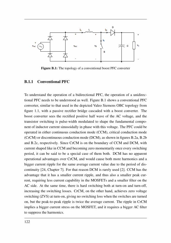
Figure B.1: The topology of a conventional boost PFC converter
B.1.1 Conventional PFC
To understand the operation of a bidirectional PFC, the operation of a unidirec-tional PFC needs to be understood as well. Figure B.1 shows a conventional PFCconverter, similar to that used in the depicted Valeo Siemens OBC topology fromfigure 1.1, with a passive rectifier bridge cascaded with a boost converter. Theboost converter sees the rectified positive half wave of the AC voltage, and thetransistor switching is pulse-width modulated to shape the fundamental compo-nent of inductor current sinusoidally in phase with this voltage. The PFC could beoperated in either continuous conduction mode (CCM), critical conduction mode(CrCM) or discontinuous conduction mode (DCM), as shown in figures B.2a, B.2band B.2c, respectively. Since CrCM is on the boundary of CCM and DCM, withcurrent shaped like in CCM and becoming zero momentarily once every switchingperiod, it can be said to be a special case of them both. DCM has no apparentoperational advantages over CrCM, and would cause both more harmonics and abigger current ripple for the same average current value due to the period of dis-continuity [24, Chapter 7]. For that reason DCM is rarely used [2]. CCM has theadvantage that it has a smaller current ripple, and thus also a smaller peak cur-rent, requiring less current capability in the MOSFETs and a smaller filter on theAC side. At the same time, there is hard switching both at turn-on and turn-off,increasing the switching losses. CrCM, on the other hand, achieves zero voltageswitching (ZVS) at turn-on, giving no switching loss when the switches are turnedon, but the peak-to-peak ripple is twice the average current. The ripple in CrCMimplies a bigger current stress on the MOSFET, and it requires a bigger AC filterto suppress the harmonics.
122
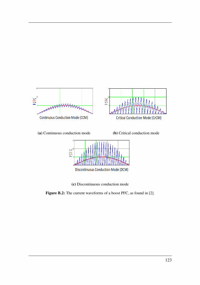
(a) Continuous conduction mode (b) Critical conduction mode
(c) Discontinuous conduction mode
Figure B.2: The current waveforms of a boost PFC, as found in [2].
123

A buck converter could also have been used in stead of a boost, but that would haverequired a big capacitor on the output of the rectifier to ensure that the voltage isalways higher than the DC-link voltage, since the buck converter needs to have anegative voltage gain in order to function [24, Chapter 7-3]. Therefore, boost PFCis a better option during charging, controlling the DC-link voltage to be higher thanthe maximum peak AC voltage (including ripple), so that the charger can operateat rated voltage during the whole input voltage range from 0 to peak.
B.1.2 Bidirectional PFC
When the boost PFC is to be made bidirectional, it is obvious that both the rectifierbridge and the freewheeling diode of the boost converter needs to be replaced.The freewheeling diode can be removed by integrating the PFC switching into therectifier bridge, as is done in several bridgeless PFC topologies in [25] and [57].The forward voltage drop of the diodes cause conduction losses [24, Chapter 2-2], so minimizing the number of diodes in the conduction path by removing thefreewheeling decreases these losses. Out of these bridgeless topologies, the basicbridgeless PFC and the totem-pole PFC are standing out with regards to simplicityand low number of semiconductors. These are depicted in figures B.3a and B.3b.For both of these topologies, the transistors are controlled such that for positiveAC-voltage half cycle one transistor is in boost PWM switching mode, while theother transistor is behaving as a rectifier diode, and oppositely in the negative halfcycle.
The totem-pole PFC was previously somewhat disregarded for the benefit of thebasic bridgeless PFC and other bridgeless PFC topologies [25]. This because thereverse recovery body diode of the MOSFET made CCM (see figure B.2) infea-sible in this topology, due to the reverse recovery current causing considerableswitching losses in CCM [24, Chapters 19 - 22]. Running it in DCM would requirevery high current ratings for higher-power applications, such as an OBC. The basicbridgeless PFC, on the other hand, does not have these issues, and has been provenin e.g. [58] to be efficient at power levels up to 3.5 kW. On the negative side,the basic bridgeless PFC produces significant amounts of common mode noise,because the zero-potential of the DC-link side is floating compared to AC groundduring negative AC mains half cycle [25, 3]. In more recent scientific works, the
124
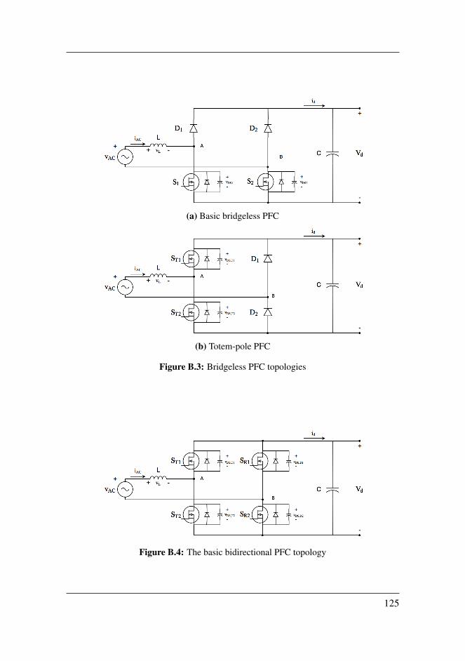
(a) Basic bridgeless PFC
(b) Totem-pole PFC
Figure B.3: Bridgeless PFC topologies
Figure B.4: The basic bidirectional PFC topology
125
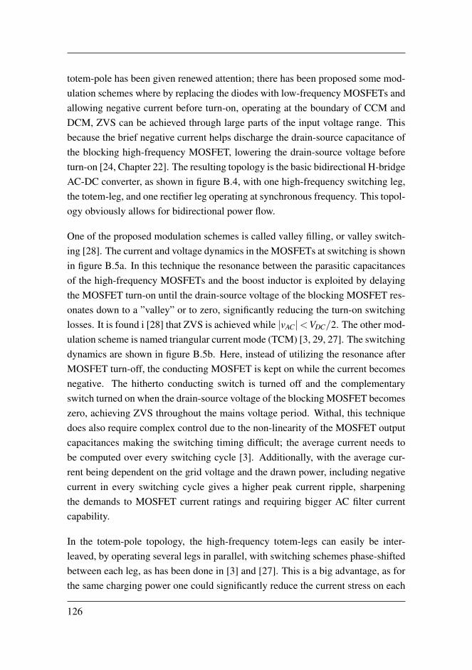
totem-pole has been given renewed attention; there has been proposed some mod-ulation schemes where by replacing the diodes with low-frequency MOSFETs andallowing negative current before turn-on, operating at the boundary of CCM andDCM, ZVS can be achieved through large parts of the input voltage range. Thisbecause the brief negative current helps discharge the drain-source capacitance ofthe blocking high-frequency MOSFET, lowering the drain-source voltage beforeturn-on [24, Chapter 22]. The resulting topology is the basic bidirectional H-bridgeAC-DC converter, as shown in figure B.4, with one high-frequency switching leg,the totem-leg, and one rectifier leg operating at synchronous frequency. This topol-ogy obviously allows for bidirectional power flow.
One of the proposed modulation schemes is called valley filling, or valley switch-ing [28]. The current and voltage dynamics in the MOSFETs at switching is shownin figure B.5a. In this technique the resonance between the parasitic capacitancesof the high-frequency MOSFETs and the boost inductor is exploited by delayingthe MOSFET turn-on until the drain-source voltage of the blocking MOSFET res-onates down to a ”valley” or to zero, significantly reducing the turn-on switchinglosses. It is found i [28] that ZVS is achieved while |vAC|<VDC/2. The other mod-ulation scheme is named triangular current mode (TCM) [3, 29, 27]. The switchingdynamics are shown in figure B.5b. Here, instead of utilizing the resonance afterMOSFET turn-off, the conducting MOSFET is kept on while the current becomesnegative. The hitherto conducting switch is turned off and the complementaryswitch turned on when the drain-source voltage of the blocking MOSFET becomeszero, achieving ZVS throughout the mains voltage period. Withal, this techniquedoes also require complex control due to the non-linearity of the MOSFET outputcapacitances making the switching timing difficult; the average current needs tobe computed over every switching cycle [3]. Additionally, with the average cur-rent being dependent on the grid voltage and the drawn power, including negativecurrent in every switching cycle gives a higher peak current ripple, sharpeningthe demands to MOSFET current ratings and requiring bigger AC filter currentcapability.
In the totem-pole topology, the high-frequency totem-legs can easily be inter-leaved, by operating several legs in parallel, with switching schemes phase-shiftedbetween each leg, as has been done in [3] and [27]. This is a big advantage, as forthe same charging power one could significantly reduce the current stress on each
126
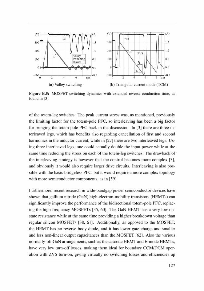
(a) Valley switching (b) Triangular current mode (TCM)
Figure B.5: MOSFET switching dynamics with extended reverse conduction time, asfound in [3].
of the totem-leg switches. The peak current stress was, as mentioned, previouslythe limiting factor for the totem-pole PFC, so interleaving has been a big factorfor bringing the totem-pole PFC back in the discussion. In [3] there are three in-terleaved legs, which has benefits also regarding cancellation of first and secondharmonics in the inductor current, while in [27] there are two interleaved legs. Us-ing three interleaved legs, one could actually double the input power while at thesame time reducing the stress on each of the totem-leg switches. The drawback ofthe interleaving strategy is however that the control becomes more complex [3],and obviously it would also require larger drive circuits. Interleaving is also pos-sible with the basic bridgeless PFC, but it would require a more complex topologywith more semiconductor components, as in [59].
Furthermore, recent research in wide-bandgap power semiconductor devices haveshown that gallium nitride (GaN) high-electron-mobility transistors (HEMTs) cansignificantly improve the performance of the bidirectional totem-pole PFC, replac-ing the high-frequency MOSFETs [35, 60]. The GaN HEMT has a very low on-state resistance while at the same time providing a higher breakdown voltage thanregular silicon MOSFETs [38, 61]. Additionally, as opposed to the MOSFET,the HEMT has no reverse body diode, and it has lower gate charge and smallerand less non-linear output capacitances than the MOSFET [62]. Also the variousnormally-off GaN arrangements, such as the cascode HEMT and E-mode HEMTs,have very low turn-off losses, making them ideal for boundary CCM/DCM oper-ation with ZVS turn-on, giving virtually no switching losses and efficiencies up
127

to 99% at 1MHz [27, 60]. Moreover, the lack of reverse body diode, lower gatecharge and smaller output capacitances reduce switching losses to such extent thata CCM-operated totem-pole becomes feasible. This is evident in [30], where a65kHz 1.5kW CCM-operated bidirectional totem-pole PFC is proven to achievean efficiency of 99%. The normally-off GaN HEMTs are however still a tech-nology in development, and few commercially available solutions exist as of now,especially at the power level of an OBC (3.5kW), but the technology in this fieldis rapidly evolving.
128
Appendix CPaper on GaN HEMTs andbidirectional PFCs
129
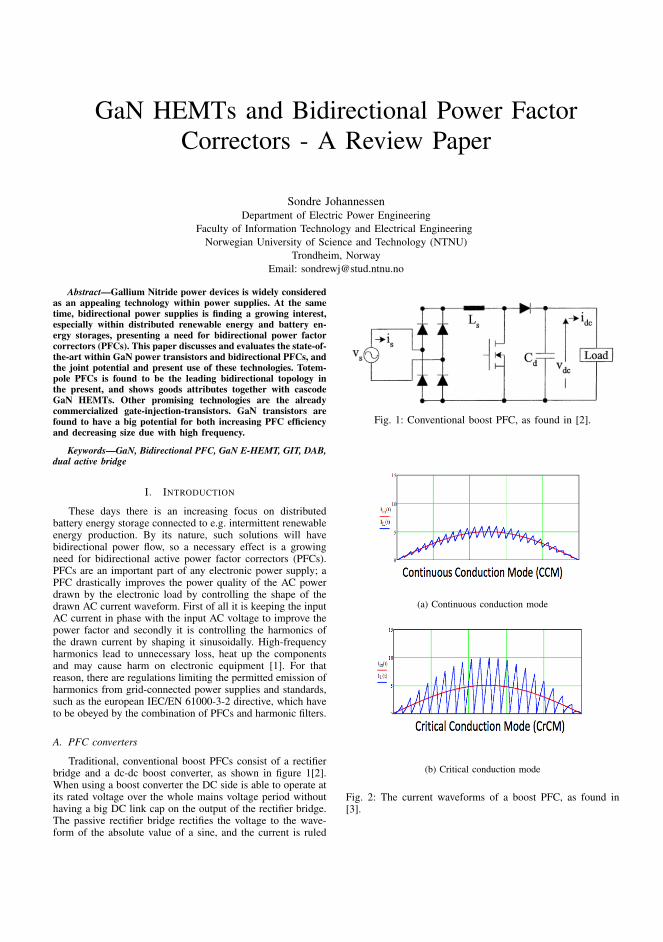
GaN HEMTs and Bidirectional Power FactorCorrectors - A Review Paper
Sondre JohannessenDepartment of Electric Power Engineering
Faculty of Information Technology and Electrical EngineeringNorwegian University of Science and Technology (NTNU)
Trondheim, NorwayEmail: [email protected]
Abstract—Gallium Nitride power devices is widely consideredas an appealing technology within power supplies. At the sametime, bidirectional power supplies is finding a growing interest,especially within distributed renewable energy and battery en-ergy storages, presenting a need for bidirectional power factorcorrectors (PFCs). This paper discusses and evaluates the state-of-the-art within GaN power transistors and bidirectional PFCs, andthe joint potential and present use of these technologies. Totem-pole PFCs is found to be the leading bidirectional topology inthe present, and shows goods attributes together with cascodeGaN HEMTs. Other promising technologies are the alreadycommercialized gate-injection-transistors. GaN transistors arefound to have a big potential for both increasing PFC efficiencyand decreasing size due with high frequency.
Keywords—GaN, Bidirectional PFC, GaN E-HEMT, GIT, DAB,dual active bridge
I. INTRODUCTION
These days there is an increasing focus on distributedbattery energy storage connected to e.g. intermittent renewableenergy production. By its nature, such solutions will havebidirectional power flow, so a necessary effect is a growingneed for bidirectional active power factor correctors (PFCs).PFCs are an important part of any electronic power supply; aPFC drastically improves the power quality of the AC powerdrawn by the electronic load by controlling the shape of thedrawn AC current waveform. First of all it is keeping the inputAC current in phase with the input AC voltage to improve thepower factor and secondly it is controlling the harmonics ofthe drawn current by shaping it sinusoidally. High-frequencyharmonics lead to unnecessary loss, heat up the componentsand may cause harm on electronic equipment [1]. For thatreason, there are regulations limiting the permitted emission ofharmonics from grid-connected power supplies and standards,such as the european IEC/EN 61000-3-2 directive, which haveto be obeyed by the combination of PFCs and harmonic filters.
A. PFC converters
Traditional, conventional boost PFCs consist of a rectifierbridge and a dc-dc boost converter, as shown in figure 1[2].When using a boost converter the DC side is able to operate atits rated voltage over the whole mains voltage period withouthaving a big DC link cap on the output of the rectifier bridge.The passive rectifier bridge rectifies the voltage to the wave-form of the absolute value of a sine, and the current is ruled
Fig. 1: Conventional boost PFC, as found in [2].
(a) Continuous conduction mode
(b) Critical conduction mode
Fig. 2: The current waveforms of a boost PFC, as found in[3].
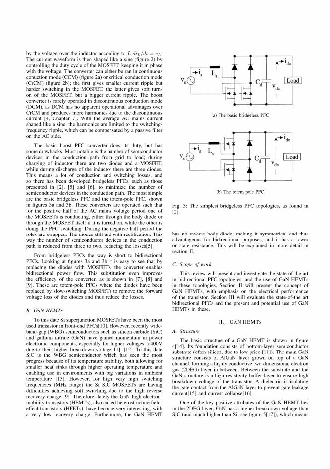
by the voltage over the inductor according to L diL/dt = vL.The current waveform is then shaped like a sine (figure 2) bycontrolling the duty cycle of the MOSFET, keeping it in phasewith the voltage. The converter can either be ran in continuousconuction mode (CCM) (figure 2a) or critical conduction mode(CrCM) (figure 2b); the first gives smaller current ripple butharder switching in the MOSFET, the latter gives soft turn-on of the MOSFET, but a bigger current ripple. The boostconverter is rarely operated in discontinuous conduction mode(DCM), as DCM has no apparent operational advantages overCrCM and produces more harmonics due to the discontinuouscurrent [4, Chapter 7]. With the average AC mains currentshaped like a sine, the harmonics are limited to the switching-frequency ripple, which can be compensated by a passive filteron the AC side.
The basic boost PFC converter does its duty, but hassome drawbacks. Most notable is the number of semiconductordevices in the conduction path from grid to load; duringcharging of inductor there are two diodes and a MOSFET,while during discharge of the inductor there are three diodes.This means a lot of conduction and switching losses, andso there has been developed bridgeless PFCs, such as thosepresented in [2], [5] and [6], to minimize the number ofsemiconductor devices in the conduction path. The most simpleare the basic bridgeless PFC and the totem-pole PFC, shownin figures 3a and 3b. These converters are operated such thatfor the positive half of the AC mains voltage period one ofthe MOSFETs is conducting, either through the body diode orthrough the MOSFET itself if it is turned on, while the other isdoing the PFC switching. During the negative half period theroles are swapped. The diodes still aid with rectification. Thisway the number of semiconductor devices in the conductionpath is reduced from three to two, reducing the losses[5].
From bridgeless PFCs the way is short to bidirectionalPFCs. Looking at figures 3a and 3b it is easy to see that byreplacing the diodes with MOSFETs, the converter enablesbidirectional power flow. This substitution even improvesthe efficiency of the converter, as is shown in [7], [8] and[9]. These are totem-pole PFCs where the diodes have beenreplaced by slow-switching MOSFETs to remove the forwardvoltage loss of the diodes and thus reduce the losses.
B. GaN HEMTs
To this date Si superjunction MOSFETs have been the mostused transistor in front-end PFCs[10]. However, recently wide-band-gap (WBG) semiconductors such as silicon carbide (SiC)and gallium nitride (GaN) have gained momentum in powerelectronic components, especially for higher voltages >400Vdue to their higher breakdown voltage[11], [12]. To this dateSiC is the WBG semiconductor which has seen the mostprogress because of its temperature stability, both allowing forsmaller heat sinks through higher operating temperature andenabling use in environments with big variations in ambienttemperature [13]. However, for high very high switchingfrequencies (MHz range) the Si SiC MOSFETs are havingdifficulties achieving soft switching due to the high reverserecovery charge [9]. Therefore, lately the GaN high-electron-mobility transistors (HEMTs), also called heterostructure field-effect transistors (HFETs), have become very interesting, witha very low recovery charge. Furthermore, the GaN HEMT
(a) The basic bridgeless PFC
(b) The totem pole PFC
Fig. 3: The simplest bridgeless PFC topologies, as found in[2].
has no reverse body diode, making it symmetrical and thusadvantageous for bidirectional purposes, and it has a loweron-state resistance. This will be explained in more detail insection II.
C. Scope of work
This review will present and investigate the state of the artin bidirectional PFC topologies, and the use of GaN HEMTsin these topologies. Section II will present the concept ofGaN HEMTs, with emphasis on the electrical performanceof the transistor. Section III will evaluate the state-of-the artbidirectional PFCs and the present and potential use of GaNHEMTs in these.
II. GAN HEMTS
A. Structure
The basic structure of a GaN HEMT is shown in figure4[14]. Its foundation consists of bottom-layer semiconductorsubstrate (often silicon, due to low price [11]). The main GaNstructure consists of AlGaN layer grown on top of a GaNchannel, forming a highly conductive two-dimensional electrongas (2DEG) layer in between. Between the substrate and theGaN structure is a high-resistivity buffer layer to ensure highbreakdown voltage of the transistor. A dielectric is isolatingthe gate contact from the AlGaN-layer to prevent gate leakagecurrent[15] and current collapse[16].
One of the key positive attributes of the GaN HEMT liesin the 2DEG layer; GaN has a higher breakdown voltage thanSiC (and much higher than Si, see figure 5[17]), which means
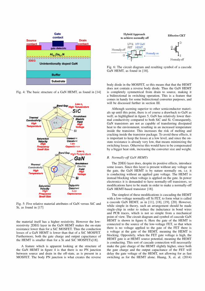
Fig. 4: The basic structure of a GaN HEMT, as found in [14]
Fig. 5: Five relative material attributes of GaN versus SiC andSi, as found in [17]
the material itself has a higher resistivity. However the low-resistivity 2DEG layer in the GaN HEMT makes the on-stateresistance lower than for a SiC MOSFET. Thus the conductionlosses of a GaN HEMT is lower than that of a SiC MOSFET.Furthermore, both the gate charge and output capacitance ofthe HEMT is smaller than for a Si and SiC MOSFETs[18].
A feature which is apparent looking at the structure ofthe GaN HEMT in figure 4 is that there is no PN junctionbetween source and drain in the off-state, as is present in aMOSFET. The body PN junction is what creates the reverse
Fig. 6: The circuit diagram and resulting symbol of a cascodeGaN HEMT, as found in [18].
body diode in the MOSFET, so this means that that the HEMTdoes not contain a reverse body diode. Thus the GaN HEMTis completely symmetrical from drain to source, making ita bidirectional in switching operation. This is a feature thatcomes in handy for some bidirectional converter purposes, andwill be discussed further in section III.
Although seeming superior to other semiconductor materi-als up until this point, there is of course a drawback to GaN aswell; as highlighted in figure 5, GaN has relatively lower ther-mal conductivity compared to both SiC and Si. Consequently,GaN transistors are not as capable of transferring dissipatedheat to the environment, resulting in an increased temperatureinside the transistor. This increases the risk of melting andcracking inside the transistor package. To avoid these effects, itis important to keep the losses at a low level, and since the on-state resistance is already very low, that means minimizing theswitching losses. Otherwise this would have to be compensatedby a bigger heat sink, increasing the converter size and weight.
B. Normally-off GaN HEMTs
The 2DEG layer does, despite its positive effects, introducesome issues. Since this layer is present without any voltage onthe gate, the GaN HEMT is by nature normally on, i.e. itis conducting without an applied gate voltage. The HEMT isinstead blocking when voltage is applied on the gate. In powerelectronics it is demanded to have normally-off transistors, somodifications have to be made in order to make a normally-offGaN HEMT-based transistor [18].
The simplest of these modifications is cascading the HEMTwith a low-voltage normally-off Si FET, to form what is calleda cascode GaN HEMT, as in [11], [18], [19], [20]. However,while simple in theory, such an arrangement should be madesingle-chip in order to reduce the inductance in bond wiresand PCB traces, which is not so simple from a mechanicalpoint of view. The circuit diagram and symbol of cascode GaNHEMT is shown in figure 6. Here the gate of the HEMT isconnected to the source of the low-voltage FET, so that whenthere is no voltage applied to the gate of the FET there isa voltage at the gate of the HEMT, meaning the HEMT isblocking. Oppositely, when the FET gate voltage is high, theHEMT gate is at HEMT source potential, meaning the HEMTis conducting. This sort of cascade connection will necessarilymake the gate charge of the HEMT slightly higher, since boththe gate charge and the output capacitance of the FET willdelay the gate voltage of the HEMT, not allowing for as fastswitching as for the HEMT alone. Huang, X. et. al. (2014)
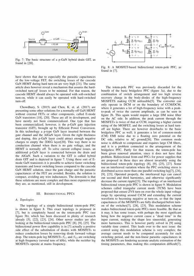
Fig. 7: The basic structure of a p-GaN hybrid drain GIT, asfound in [20].
have shown that due to especially the parasitic capacitancesof the low-voltage FET, the switching losses of the cascodeGaN HEMT during hard turn-on are very high [21]. The samearticle does however reveal a mechanism that assures the hard-switched turn-off losses to be minimal. For that reason, thecascode HEMT should always be operated with soft-switchedturn-on, while it can easily be operated with hard-switchedturn-off.
Chowdhury, S. (2015) and Chen, K. et. al. (2017) arepresenting some other solutions for a normally-off GaN HEMTwithout external FETs or other components, called E-modeGaN transistors [18], [20]. These are all in development, andhave mostly not been commercialized. One type that hasbeen commercialized, however, is the p-GaN gate injectiontransistor (GIT), brought up by Efficient Power Conversion.In this technology a p-type GaN layer inserted between thegate channel and the AlGaN layer. Given the right thicknessand doping, this p-GaN layer could attract enough negativecharges to empty the 2DEG layer[20]. This way there is noconduction channel when there is no gate voltage, and theHEMT is normally off. To solve current collapse issues, anadditional p-GaN layer is connected between the drain andthe AlGaN. Such a variation to the GIT is called hybriddrain GIT and is depicted in figure 7. Using these sort of E-mode GaN transistors it is possible to achieve faster switchingtransients and lower switching losses compared to the cascodeGaN HEMT solution, since the gate charge and the parasiticcapacitances of the FET are avoided. Besides, the solution iscompact, avoiding any wire inductances. The downside is thatthese solutions are more complex and thus more expensive andthey are, as mentioned, still in development.
III. BIDIRECTIONAL PFCS
A. Topologies
The topology of a simple bidirectional totem-pole PFCis shown in figure 8. This exact topology is proposed in[7], but is completely based on the totem-pole PFC (seefigure 3b), which has been discussed in plenty of researchalready [5], [22], [23], [24]. Other newer studies are alsolooking at the bidirectional totem-pole PFC [8], [9], [25]. Thebidirectional power flow capability is in [7] actually a positiveside effect of the substitution of diodes with MOSFETs toreduce conduction losses by removing diode forward voltagedrop. The totem-pole leg MOSFETs S11 and S12 are switchingat high frequency (several tens of kHz), while the rectifier legMOSFETs operate at mains frequency.
Fig. 8: A MOSFET-based bidirectional totem-pole PFC, asfound in [7].
The totem-pole PFC was previously discarded for thebenefit of the basic bridgeless PFC (figure 3a), due to thecombination of switch arrangement and too high reverserecovery charge in the body-diodes of the high-frequencyMOSFETS making CCM unfeasible[5]. The converter canonly operate in DCM or on the boundary of CCM/DCM,where it generates a lot of high-frequency noise with a peak-to-peak of twice the current amplitude, as can be seen infigure 2b. This again would require a large DM noise filteron the AC side. In addition, the peak current through theMOSFETs is twice of that at CCM, requiring a higher currentrating of the MOSFET, and the switching losses at hard turn-off are higher. There are however drawbacks to the basicbridgeless PFC as well; it generates a lot of common-mode(CM) EMI noise due to a floating zero potential on theDC side, relative to AC ground[26]. This common modenoise is difficult to compensate and requires large CM filters,and it is a problem connected to the arrangement of thebridgeless PFC. Partly for that reason, the totem-pole hasbeen given renewed attention, since it does not have thatproblem. Bidirectional front-end PFCs for power supplies thatare proposed in these days are almost invariably using thebidirectional totem-pole topology [8], [9], [25], [27]. Someuse an interleaved variation where the PFC switching stress isdistributed across more than one parallel switching leg[7], [24],[9], [23]. Operated properly, the interleaved legs can cancelout second and third harmonics, and otherwise significantlydecrease the current ripple[23]. The topology of an interleavedbidirectional totem-pole PFC is shown in figure 9. Modulationschemes called triangular current mode (TCM) have beenproposed that ensure ZVS turn-on over the whole input voltagerange by operating around CrCM and extending the currentwaveform to becoming negative at turn-on, so that the inputcapacitances of the MOSFETs are fully discharged before turn-on of the switches[7], [28], [23]. This modulation schememakes bidirectional totem-pole PFCs more feasible. Be that asit may, it has some issues, with perhaps the most significantbeing how the negative current cause a ”dead time” in theinput current, making the shape less sinusoidal, generatingmore harmonics. This is however partly solved in [9] usingvariable time control. This leads over to the next issue: thecontrol using this modulation scheme is very complex; theaverage current needs to be computed accurately for eachswitching period, and the non-linear parasitic capacitances inthe MOSFETs are hindering accurate analytic estimation of thetiming parameters, thus making this computation difficult[7].
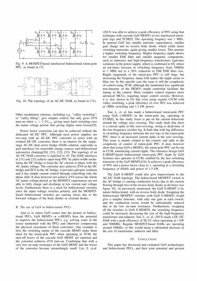
Fig. 9: A MOSFET-based interleaved bidirectional totem-polePFC, as found in [7].
Fig. 10: The topology of an AC-DC DAB, as found in [31].
Other modulation schemes, including e.g. ”valley switching”,or ”valley filling”, give simpler control, but only gives ZVSturn-on when vs < 1/2Vout, giving more hard switching overthe mains voltage period, thus giving slighty more losses[29].
Power factor correction can also be achieved without thededicated AC-DC PFC. Although most power supplies aretwo-step with an AC-DC PFC converter in series with anisolated DC-DC converter, there is an interest for the single-stage AC-DC dual active bridge (DAB) solution, especially asgrid interfaces for renewable energy sources and bidirectionalautomotive charging[30], [31], [32], [33]. The topology of anAC-DC DAB converter is depicted in 10. The DAB interfacesin [31] and [32] achieve open-loop PFC by pulse-width modu-lating the DC bridge to keep the AC current in phase with theAC mains voltage. The converter also achieves ZVS in the DCbridge and ZCS in the AC bridge, it provides galvanic isolationand it has simple current control through controlling only thephase shift. It does however not achieve ZVS across the wholeAC mains voltage period, as the MOSFET capacitances are notable to fully charge and discharge at low current and voltagelevels. Furthermore there is a need for bidirectional switchessince the input voltage switches polarity, and the MOSFET-based bidirectional switches are causing losses due to theforward voltages of the body diodes or external diodes.
B. The use of GaN in bidirectional PFCs
And so to where GaN comes into the picture in bidirec-tional PFCs. GaN HEMTs or e-HEMTs have the potentialto improve the bidirectional PFCs, e.g. solving some of theissues mentioned with the PFCs and otherwise compressingthe physical executions of these converters. One example ishow the switching nature of the cascode HEMT make themideal for the totem-pole PFC when operating in TCM; theturn-off losses of the cascode GaN HEMT are minimal andthe converter achieves ZVS turn-on. Combining that with avery low on-state resistance of the GaN HEMT and the lossesof the converter become astonishingly small. Liu, Z. et.al.
(2015) was able to achieve a peak efficiency of 99% using thattechnique with cascode GaN HEMTs in two interleaved totem-pole legs and TCM[9]. The operating frequncy was 1 MHz.In general GaN has smaller parasitic capacitances, smallergate charge and no reverse body diode, which yields fasterswitching transients, again giving smaller losses. This permitsa higher switching frequency. Higher frequency ripple allowsfor smaller EMI filter and smaller magnetic components,such as inductors and high-frequency transformers (galvanicisolation) in the power supply, which is confirmed in [9], wherean ten-times increase in switching frequency from 100kHzto 1 MHz led to a 50% reduction in DM EMI filter size.Ripple magnitude of the totem-poe PFC is still large, butincreasing the frequency many-fold makes the ripple easier tofilter out. In this specific case the issue is still the complexityof control using TCM, although the mentioned less significantnon-linearity of the HEMTs might somewhat facilitate thetiming in the control. More complex control requires moreadvanced MCUs, requiring larger control circuits. However,it is also shown in [9] that even using regular CrCM withvalley switching, a peak efficiency of over 98% was achievedat 1MHz switching and 1.2 kW power.
Xue, L. et. al. has made a bidirectional totem-pole PFCusing GaN e-HEMTs in the totem-pole leg, operating inCCM[8]. In this study, focus is put on the current behaviouraround the voltage zero crossing. This study finds that thereis a current spike at this zero-crossing, owing to dead-time ofthe low-frequency rectifier leg. It finds that with big differencein switching frequency between the two legs of the totem-polePFC, there is an increased current spike at the zero crossing.This issue is mainly related to the control, and adds to thecomplexity of control of totem-pole PFC. It does howevershow that using GaN e-HEMTs, the totem-pole PFC can be ranin CCM, minimizing current ripple. The reference design GaNE-HEMT-based bidirectional totem-pole PFC made by GaNSystems also operates in CCM, enabled by the fast switchingtransients of the GaN HEMTs[34]. It achieves a peak efficiencyof 99% and a power factor close to 1, operating at a switchingfrequency of 65kHz and power of 1.5 kW.
The GaN E-HEMT could also give improvement to theAC-DC DAB topology. The bidirectional MOSFET switch inthe AC-bridge is causing conduction losses due to the currentflowing through two of the reverse body diodes at all times (seefigure 10). As previously mentioned, the GaN E-HEMT is bynature bidirectional, with no reverse body diode. Swapping thebidirectional MOSFET switches with GaN E-HEMTs wouldgive a simpler structure, with only one gate at each switch,and the conduction losses would be substantially reduceddue to the low on-state resistance. Furthermore, swappingall the switches to GaN E-HEMTS, the switching frequencycould be increased, decreasing the size of the high-frequencytransformer and inductor. Xue, L. et. al. (2015) made a DC-DCDAB with a peak efficiency of 98.2% when operating at 1 kWand 500MHz. Regular MOSFET-based DABs are operatingaround 100kHz, so this would mean a substantial decrease inthe size of transformer, inductor and filter.
IV. CONCLUSION
This paper has discussed and evaluated GaN technologiesand bidirectional PFCs, and their joint potential and present
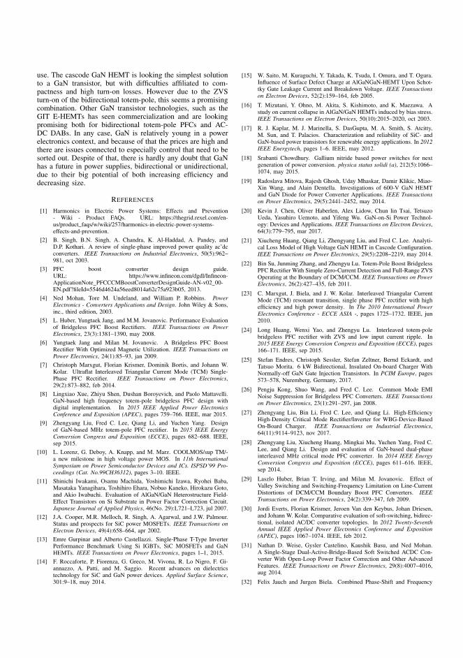
use. The cascode GaN HEMT is looking the simplest solutionto a GaN transistor, but with difficulties affiliated to com-pactness and high turn-on losses. However due to the ZVSturn-on of the bidirectional totem-pole, this seems a promisingcombination. Other GaN transistor technologies, such as theGIT E-HEMTs has seen commercialization and are lookingpromising both for bidirectional totem-pole PFCs and AC-DC DABs. In any case, GaN is relatively young in a powerelectronics context, and because of that the prices are high andthere are issues connected to especially control that need to besorted out. Despite of that, there is hardly any doubt that GaNhas a future in power supplies, bidirectional or unidirectional,due to their big potential of both increasing efficiency anddecreasing size.
REFERENCES
[1] Harmonics in Electric Power Systems: Effects and Prevention- Wiki - Product FAQs. URL: https://thegrid.rexel.com/en-us/product faqs/w/wiki/257/harmonics-in-electric-power-systems-effects-and-prevention.
[2] B. Singh, B.N. Singh, A. Chandra, K. Al-Haddad, A. Pandey, andD.P. Kothari. A review of single-phase improved power quality ac˜dcconverters. IEEE Transactions on Industrial Electronics, 50(5):962–981, oct 2003.
[3] PFC boost converter design guide.URL: https://www.infineon.com/dgdl/Infineon-ApplicationNote PFCCCMBoostConverterDesignGuide-AN-v02 00-EN.pdf?fileId=5546d4624a56eed8014a62c75a923b05, 2013.
[4] Ned Mohan, Tore M. Undeland, and William P. Robbins. PowerElectronics - Converters Applications and Design. John Wiley & Sons,inc., third edition, 2003.
[5] L. Huber, Yungtaek Jang, and M.M. Jovanovic. Performance Evaluationof Bridgeless PFC Boost Rectifiers. IEEE Transactions on PowerElectronics, 23(3):1381–1390, may 2008.
[6] Yungtaek Jang and Milan M. Jovanovic. A Bridgeless PFC BoostRectifier With Optimized Magnetic Utilization. IEEE Transactions onPower Electronics, 24(1):85–93, jan 2009.
[7] Christoph Marxgut, Florian Krismer, Dominik Bortis, and Johann W.Kolar. Ultraflat Interleaved Triangular Current Mode (TCM) Single-Phase PFC Rectifier. IEEE Transactions on Power Electronics,29(2):873–882, feb 2014.
[8] Lingxiao Xue, Zhiyu Shen, Dushan Boroyevich, and Paolo Mattavelli.GaN-based high frequency totem-pole bridgeless PFC design withdigital implementation. In 2015 IEEE Applied Power ElectronicsConference and Exposition (APEC), pages 759–766. IEEE, mar 2015.
[9] Zhengyang Liu, Fred C. Lee, Qiang Li, and Yuchen Yang. Designof GaN-based MHz totem-pole PFC rectifier. In 2015 IEEE EnergyConversion Congress and Exposition (ECCE), pages 682–688. IEEE,sep 2015.
[10] L. Lorenz, G. Deboy, A. Knapp, and M. Marz. COOLMOS/sup TM/-a new milestone in high voltage power MOS. In 11th InternationalSymposium on Power Semiconductor Devices and ICs. ISPSD’99 Pro-ceedings (Cat. No.99CH36312), pages 3–10. IEEE.
[11] Shinichi Iwakami, Osamu Machida, Yoshimichi Izawa, Ryohei Baba,Masataka Yanagihara, Toshihiro Ehara, Nobuo Kaneko, Hirokazu Goto,and Akio Iwabuchi. Evaluation of AlGaN/GaN Heterostructure Field-Effect Transistors on Si Substrate in Power Factor Correction Circuit.Japanese Journal of Applied Physics, 46(No. 29):L721–L723, jul 2007.
[12] J.A. Cooper, M.R. Melloch, R. Singh, A. Agarwal, and J.W. Palmour.Status and prospects for SiC power MOSFETs. IEEE Transactions onElectron Devices, 49(4):658–664, apr 2002.
[13] Emre Gurpinar and Alberto Castellazzi. Single-Phase T-Type InverterPerformance Benchmark Using Si IGBTs, SiC MOSFETs and GaNHEMTs. IEEE Transactions on Power Electronics, pages 1–1, 2015.
[14] F. Roccaforte, P. Fiorenza, G. Greco, M. Vivona, R. Lo Nigro, F. Gi-annazzo, A. Patti, and M. Saggio. Recent advances on dielectricstechnology for SiC and GaN power devices. Applied Surface Science,301:9–18, may 2014.
[15] W. Saito, M. Kuraguchi, Y. Takada, K. Tsuda, I. Omura, and T. Ogura.Influence of Surface Defect Charge at AlGaNGaN-HEMT Upon Schot-tky Gate Leakage Current and Breakdown Voltage. IEEE Transactionson Electron Devices, 52(2):159–164, feb 2005.
[16] T. Mizutani, Y. Ohno, M. Akita, S. Kishimoto, and K. Maezawa. Astudy on current collapse in AlGaN/GaN HEMTs induced by bias stress.IEEE Transactions on Electron Devices, 50(10):2015–2020, oct 2003.
[17] R. J. Kaplar, M. J. Marinella, S. DasGupta, M. A. Smith, S. Atcitty,M. Sun, and T. Palacios. Characterization and reliability of SiC- andGaN-based power transistors for renewable energy applications. In 2012IEEE Energytech, pages 1–6. IEEE, may 2012.
[18] Srabanti Chowdhury. Gallium nitride based power switches for nextgeneration of power conversion. physica status solidi (a), 212(5):1066–1074, may 2015.
[19] Radoslava Mitova, Rajesh Ghosh, Uday Mhaskar, Damir Klikic, Miao-Xin Wang, and Alain Dentella. Investigations of 600-V GaN HEMTand GaN Diode for Power Converter Applications. IEEE Transactionson Power Electronics, 29(5):2441–2452, may 2014.
[20] Kevin J. Chen, Oliver Haberlen, Alex Lidow, Chun lin Tsai, TetsuzoUeda, Yasuhiro Uemoto, and Yifeng Wu. GaN-on-Si Power Technol-ogy: Devices and Applications. IEEE Transactions on Electron Devices,64(3):779–795, mar 2017.
[21] Xiucheng Huang, Qiang Li, Zhengyang Liu, and Fred C. Lee. Analyti-cal Loss Model of High Voltage GaN HEMT in Cascode Configuration.IEEE Transactions on Power Electronics, 29(5):2208–2219, may 2014.
[22] Bin Su, Junming Zhang, and Zhengyu Lu. Totem-Pole Boost BridgelessPFC Rectifier With Simple Zero-Current Detection and Full-Range ZVSOperating at the Boundary of DCM/CCM. IEEE Transactions on PowerElectronics, 26(2):427–435, feb 2011.
[23] C. Marxgut, J. Biela, and J. W. Kolar. Interleaved Triangular CurrentMode (TCM) resonant transition, single phase PFC rectifier with highefficiency and high power density. In The 2010 International PowerElectronics Conference - ECCE ASIA -, pages 1725–1732. IEEE, jun2010.
[24] Long Huang, Wenxi Yao, and Zhengyu Lu. Interleaved totem-polebridgeless PFC rectifier with ZVS and low input current ripple. In2015 IEEE Energy Conversion Congress and Exposition (ECCE), pages166–171. IEEE, sep 2015.
[25] Stefan Endres, Christoph Sessler, Stefan Zeltner, Bernd Eckardt, andTatsuo Morita. 6 kW Bidirectional, Insulated On-board Charger WithNormally-off GaN Gate Injection Transistors. In PCIM Europe, pages573–578, Nuremberg, Germany, 2017.
[26] Pengju Kong, Shuo Wang, and Fred C. Lee. Common Mode EMINoise Suppression for Bridgeless PFC Converters. IEEE Transactionson Power Electronics, 23(1):291–297, jan 2008.
[27] Zhengyang Liu, Bin Li, Fred C. Lee, and Qiang Li. High-EfficiencyHigh-Density Critical Mode Rectifier/Inverter for WBG-Device-BasedOn-Board Charger. IEEE Transactions on Industrial Electronics,64(11):9114–9123, nov 2017.
[28] Zhengyang Liu, Xiucheng Huang, Mingkai Mu, Yuchen Yang, Fred C.Lee, and Qiang Li. Design and evaluation of GaN-based dual-phaseinterleaved MHz critical mode PFC converter. In 2014 IEEE EnergyConversion Congress and Exposition (ECCE), pages 611–616. IEEE,sep 2014.
[29] Laszlo Huber, Brian T. Irving, and Milan M. Jovanovic. Effect ofValley Switching and Switching-Frequency Limitation on Line-CurrentDistortions of DCM/CCM Boundary Boost PFC Converters. IEEETransactions on Power Electronics, 24(2):339–347, feb 2009.
[30] Jordi Everts, Florian Krismer, Jeroen Van den Keybus, Johan Driesen,and Johann W. Kolar. Comparative evaluation of soft-switching, bidirec-tional, isolated AC/DC converter topologies. In 2012 Twenty-SeventhAnnual IEEE Applied Power Electronics Conference and Exposition(APEC), pages 1067–1074. IEEE, feb 2012.
[31] Nathan D. Weise, Gysler Castelino, Kaushik Basu, and Ned Mohan.A Single-Stage Dual-Active-Bridge-Based Soft Switched ACDC Con-verter With Open-Loop Power Factor Correction and Other AdvancedFeatures. IEEE Transactions on Power Electronics, 29(8):4007–4016,aug 2014.
[32] Felix Jauch and Jurgen Biela. Combined Phase-Shift and Frequency

Modulation of a Dual-Active-Bridge AC-DC Converter with PFC. IEEETransactions on Power Electronics, 31(12), 2016.
[33] Rohit Baranwal, Gysler F. Castelino, Kartik Iyer, Kaushik Basu, andNed Mohan. A Dual-Active-Bridge-Based Single-Phase AC to DCPower Electronic Transformer With Advanced Features. IEEE Trans-actions on Power Electronics, 33(1):313–331, jan 2018.
[34] High Efficiency CCM Bridgeless Totem Pole PFCDesign using GaN E-HEMT Reference Design. URL:http://www.gansystems.com/ includes/ckfinder/userfiles/files/GS665BTP-REF%20rev170905.pdf.

Appendix D
D.1 Modulus Optimum in current loop
D.1.1 PI controller parameters
Choosing Ti,i = L/RL and implementing to (4.21), the open-loop transfer functioncan be reduced to:
Hol,i(s) =Kp,i
L· 1
s · (1+Tsum,i · s), (D.1)
giving the following closed-loop transfer function:
Hcl,i(s) =iAC(s)
iAC,re f (s)=
11+ L
Kp,i· s+ LTsum
Kp,i· s2
. (D.2)
Comparing (D.2) to the standard equation for a second-order system, which is
H2.order(s) =1
1+2ζs
ω0+( s
ω0
)2 , (D.3)
expressions for the relative damping ζ and the resonant frequency ω0 can be foundas
137

ζ =12
√L
Kp,i ·Tsum,i, ω0 =
√Kp,i
L ·Tsum,i. (D.4)
In modulus optimum, it is common setting ζ = 1/√
2. [40, ch. 3.2.3] Implement-ing that to (D.4), an expression for the proportional gain can be found, giving thefollowing controller parameters:
Kp,i =L
2 ·Tsum,i, Ti,i =
LRL
. (D.5)
D.1.2 Current measurement filter design with Modulus optimum
As explained in section 4.2.2, the integrator time constant limits the ripple of thecontrol signal, in this case d. The control signal ripple is caused by the proportionalgain on the measured ripple. Acknowledging this and neglecting the integratorpart of the PI as well as the reference current, which has no ripple, the followingexpression can be obtained based on figure 4.7 and (4.15): [40, ch. 3.4.1]
dripple(s)iAC,ripple(s)
= Kp,i ·1
1+Tf i,i · s. (D.6)
Based on D.6, the amplitude of the ripple can be expressed as follows:
dripple(ωripple) = Kp,i ·1√
1+(ωrippleTf i,i)2· 1
2∆IL(ωripple) . (D.7)
Substituting the expression for Kp,i in D.5 into (??), an expression for the dutycycle ripple can be given as follows:
dripple(ωripple) =L
2 ·Tsum,i· 1√
1+(ωrippleTf i,i)2· 1
2∆IL(ωripple) . (D.8)
It is stated in [40, 3.4.1] that the control voltage ripple amplitude, in this casedripple, should be kept at values between 0.04 and 0.08, to avoid the controlleritself generating harmonics while still limiting the delay of the filter. Solving (D.8)
138
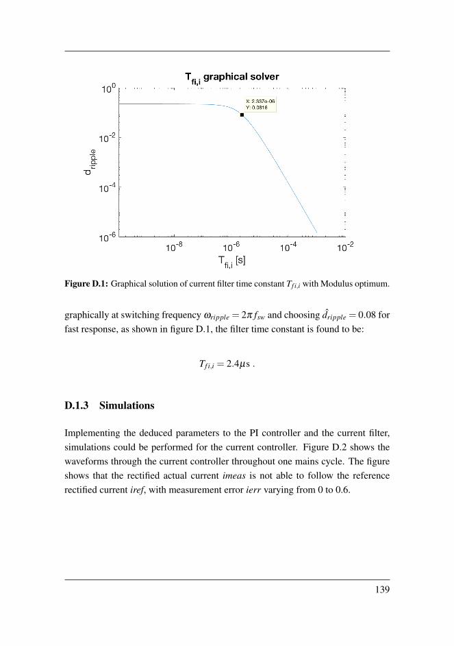
Figure D.1: Graphical solution of current filter time constant Tf i,i with Modulus optimum.
graphically at switching frequency ωripple = 2π fsw and choosing dripple = 0.08 forfast response, as shown in figure D.1, the filter time constant is found to be:
Tf i,i = 2.4µs .
D.1.3 Simulations
Implementing the deduced parameters to the PI controller and the current filter,simulations could be performed for the current controller. Figure D.2 shows thewaveforms through the current controller throughout one mains cycle. The figureshows that the rectified actual current imeas is not able to follow the referencerectified current iref, with measurement error ierr varying from 0 to 0.6.
139
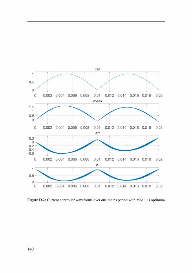
Figure D.2: Current controller waveforms over one mains period with Modulus optimum
140

Appendix EImplemented Simulink model
141
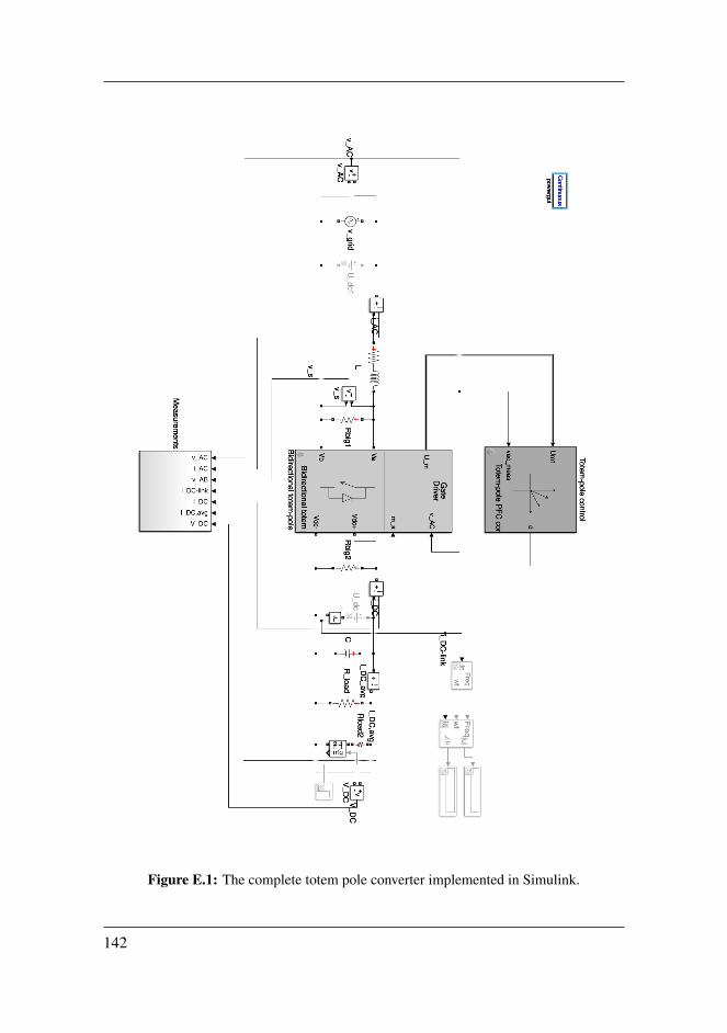
Figure E.1: The complete totem pole converter implemented in Simulink.
142
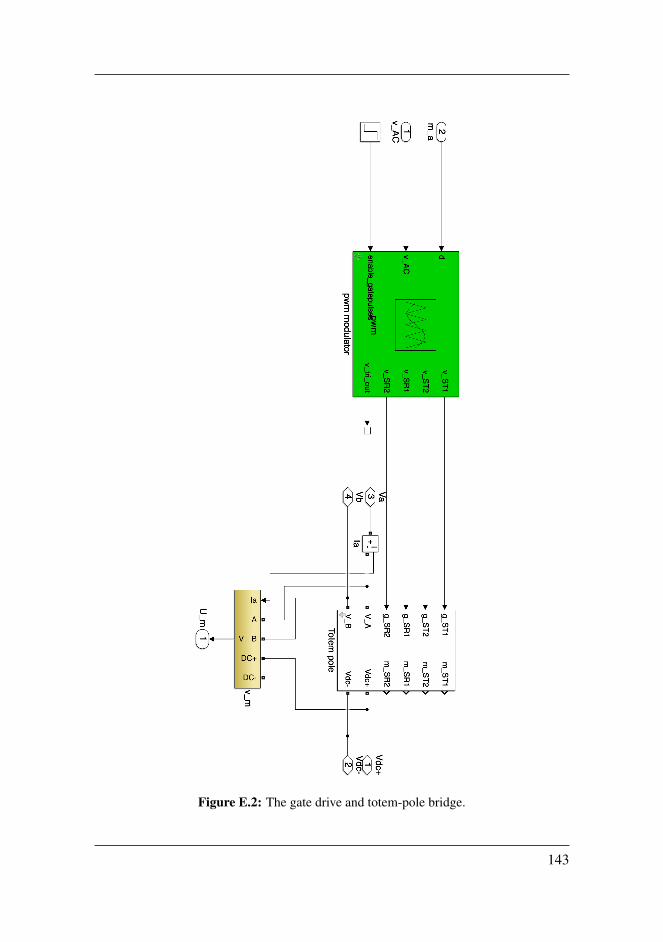
Figure E.2: The gate drive and totem-pole bridge.
143
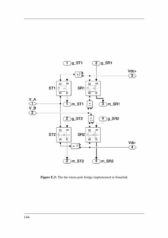
Figure E.3: The the totem-pole bridge implemented in Simulink
144

Appendix FMATLAB code
F.1 Controller tuning script
1
2 % Chosen p a r a m e t e r s3
4 Vac = 230 ; %V5 Vacpeak = s q r t ( 2 ) ∗Vac ; %V6 Vdc = 340 ; %V7 Vdcmax = 400 ; %V8 I a c = 1 6 ; %A9 I a c p e a k = s q r t ( 2 ) ∗ I a c ; %A
10 Pac = Vac∗ I a c ; %W11 fsw = 90 e +03; %Hz12 wsw = 2∗ p i ∗ fsw ; %Hz13 f g r i d = 5 0 ; %Hz14
15 K i r i p p l e = 0 . 2 ; % peak−to−peak c u r r e n t r i p p l e f a c t o r[%/100%]
16 K v r i p p l e = 0 . 1 ; % peak−to−peak s w i t c h i n g f r e q u e n c yv o l t a g e r i p p l e [%/100%]
145

17 ILpeak2peak = K i r i p p l e ∗ I a c p e a k ; %A18 VCpeak2peak = 2 0 ; %V19 Kvdc = VCpeak2peak / Vdc ;20
21
22 %Base v a l u e s23
24 Vbase = Vdc ;25 I b a s e = 16∗ s q r t ( 2 ) ;26 Rbase = Vbase / I b a s e ;27
28
29 % Component d i m e n s i o n i n g30
31 L = 0 .25∗Vdcmax / ( ILpeak2peak ∗ fsw ) ; %H32 C = 1 . 8 e−3; %F33
34
35
36
37 %% CURRENT CONTROLLER d e s i g n u s i n g PI and SYMMETRICALOPTIMUM
38
39 %Base v a l u e s40 Vbase = Vdc ;41 I b a s e = 16∗ s q r t ( 2 ) ;42 Rbase = Vbase / I b a s e ;43
44 %PU p a r a m e t e r s45 Lpu = L / Rbase ;46
47 %Time c o n s t a n t s and g a i n s48 Tpwm = 1 / ( 3∗ fsw ) ;49 f c i = 10 ˆ ( −0 .8 ) ∗ fsw ;50 Kfi = 1 ;
146

51 Kreg i = 1 ;52 T f i =2 .7 e−6;53 Tsum i = T f i +Tpwm;54
55 %Symmet r i ca l optimum56 b e t a i = 1 / ( 2∗ p i ∗ f c i ∗Tsum i ) ˆ 2 ;57 T i i = b e t a i ∗Tsum i ;58 Kpi = Lpu∗Kreg i / ( Kf i ∗ s q r t ( b e t a i ) ∗Tsum i ) ;59
60 d i s p l a y ( T i i )61 d i s p l a y ( Kpi )62
63
64 %Bode p l o t65 H o l i = t f ( Kpi / ( L∗ T i i ) ∗ [ T i i 1 ] , [ Tsum i 1 0 0 ] ) ;66 % bode ( H o l i )67
68
69
70 %% CURRRENT CONTROLLER d e s i g n u s i n g PI and MODULUSOPTIMUM
71
72 Rl = 10e−03; %P a r a s i t i c r e s i s t a n c e o f73
74 %Base v a l u e s75 Vbase = Vdc ;76 I b a s e = 16∗ s q r t ( 2 ) ;77 Rbase = Vbase / I b a s e ;78
79 %PU p a r a m e t e r s80 Lpu = L / Rbase ;81 Rlpu = Rl / Rbase ;82
83 %Time c o n s t a n t s and g a i n s84 Tl = L / Rl ;
147

85 Tpwm = 1 / ( 3∗ fsw ) ;86 T f i = 2 . 4 e−6;87 Tsum i = Tpwm+ T f i ;88
89 f 0 i = 1 / ( 2∗ p i ∗ s q r t ( 2 ) ∗Tsum i ) ;90
91 %Modulus optimum92 T i i = Tl ;93 Ks = 1 ;94 Kpi = Lpu / ( 2 ∗Ks∗Tsum i ) ;95
96 d i s p l a y ( T i i )97 d i s p l a y ( Kpi )98
99 %C r o s s o v e r f r e q u e n c y ( cu t−o f f f r e q u e n c y )100 wc2 = −1/(2∗ Tsum i ˆ 2 ) + s q r t ( 1 / ( 4 ∗ Tsum i ˆ 4 ) +( Kpi∗Ks / ( Lpu
∗Tsum i ) ) ˆ 2 ) ;101 wc = s q r t ( wc2 ) ;102 f c = wc / ( 2 ∗ p i ) ;103
104
105 Bode p l o t106 H o l i = t f ( Kpi / L , [ Tsum i 1 0 ] ) ;107
108 bode ( H o l i )109
110
111 %% V o l t a g e c o n t r o l l e r d e s i g n u s i n g s y m m e t r i c a l optimum112
113 %PU p a r a m e t e r s114 Cpu = C / Rbase ;115
116 %Time c o n s t a n t s and g a i n s117 f f i v = 2 0 ; %F i l t e r cu t−o f f f r e q u e n c y118 T f i v = 1∗10ˆ(−4) ;%1 / f f i v ; %Time c o n s t a n t
148

119 Tsum v = T f i v +2∗Tsum i ; %Sum of d e l a y s120
121 f c v = 500 ;%10ˆ ( −0 .7 ) ∗ f c i ; %V o l t a g e loop c u t o f ff r e q u e n c y
122 Kfiv = 1 ;123 Kregv = 1 ;124
125 %Symmet r i ca l optimum126 b e t a v = 1 / ( 2∗ p i ∗ f c v ∗Tsum v ) ˆ 2 ;127 Tiv = b e t a v ∗Tsum v ;128 Kpv = Cpu∗Kregv / ( Kf iv ∗ s q r t ( b e t a v ) ∗Tsum v ) ;129
130
131 d i s p l a y ( Tiv ) ;132 d i s p l a y ( Kpv ) ;
F.2 Filter graphical solver
1 %−−> F i l t e r t ime c o n s t a n t ( Be longs t oT o t e m p o l e s c r i p t .m, which needs t o be run f i r s t )
2
3 %% C u r r e n t c o n t r o l l e r w i th Modulus optimum4
5 T f i s t e p = 1e−10;6 Tfimax = 1e−03;7 T f i v e c t o r = 0 : T f i s t e p : Tfimax ;8 m a r i p p l e = z e r o s ( 1 , l e n g t h ( T f i v e c t o r ) ) ;9
10 f o r i = 1 : l e n g t h ( T f i v e c t o r )11 m a r i p p l e ( i ) = 1 /2∗ K i r i p p l e ∗Lpu / ( 2 ∗ ( Tpwm+ T f i v e c t o r
( i ) ) ∗ s q r t ( 1 + ( T f i v e c t o r ( i ) ∗2∗ p i ∗ fsw ) ˆ 2 ) ) ;12 end13
14 c l o s e a l l15 f i g u r e
149

16 l o g l o g ( T f i v e c t o r , m a r i p p l e )17 t i t l e ( ’ T f i , i g r a p h i c a l s o l v e r ’ )18 x l a b e l ( ’ T f i , i [ s ] ’ )19 y l a b e l ( ’ d r i p p l e ’ )20 s e t ( gca , ’ f o n t s i z e ’ , 1 8 )21
22
23 %% C u r r e n t c o n t r o l l e r w i th Symmet r i c a l optimum24
25 wci = 2∗ p i ∗ f c i ;26
27 T f i s t e p = 1e−10;28 Tfimax = 1e−03;29 T f i v e c t o r = 0 : T f i s t e p : Tfimax ;30 m a r i p p l e = z e r o s ( 1 , l e n g t h ( T f i v e c t o r ) ) ;31
32 f o r i = 1 : l e n g t h ( T f i v e c t o r )33 m a r i p p l e ( i ) = 1 /2∗ K i r i p p l e ∗Lpu∗wci / s q r t ( 1 + (
T f i v e c t o r ( i ) ∗2∗ p i ∗ fsw ) ˆ 2 ) ;34 end35
36 c l o s e a l l37 f i g u r e38 l o g l o g ( T f i v e c t o r , m a r i p p l e )39 t i t l e ( ’ T f i , i g r a p h i c a l s o l v e r ’ )40 x l a b e l ( ’ T f i , i [ s ] ’ )41 y l a b e l ( ’ d r i p p l e ’ )42 s e t ( gca , ’ f o n t s i z e ’ , 1 8 )43
44
45 %% V o l t a g e c o n t r o l l e r w i th s y m m e t r i c a l optimum46
47 wcv = 2∗ p i ∗500 ;48
49 T f v s t e p = 1e−8;
150

50 Tfvmax = 1e−02;51 T f v v e c t o r = 1e−6: T f v s t e p : Tfvmax ;52 i c t r l r i p p l e = z e r o s ( 1 , l e n g t h ( T f v v e c t o r ) ) ;53
54 f o r i = 1 : l e n g t h ( T f v v e c t o r )55 i c t r l r i p p l e ( i ) = 1 /2∗Kvdc∗Cpu∗wcv / s q r t ( 1 + (
T f v v e c t o r ( i ) ∗2∗ p i ∗2∗ f g r i d ) ˆ 2 ) ;56 end57
58 c l o s e a l l59 f i g u r e60 l o g l o g ( T f v v e c t o r , i c t r l r i p p l e )61 t i t l e ( ’ T f i , v g r a p h i c a l s o l v e r ’ )62 x l a b e l ( ’ T f i , v [ s ] ’ )63 y l a b e l ( ’ i c t r l , r i p p l e ’ )64 s e t ( gca , ’ f o n t s i z e ’ , 1 8 )
151

152
Appendix GSystem-level simulations
153
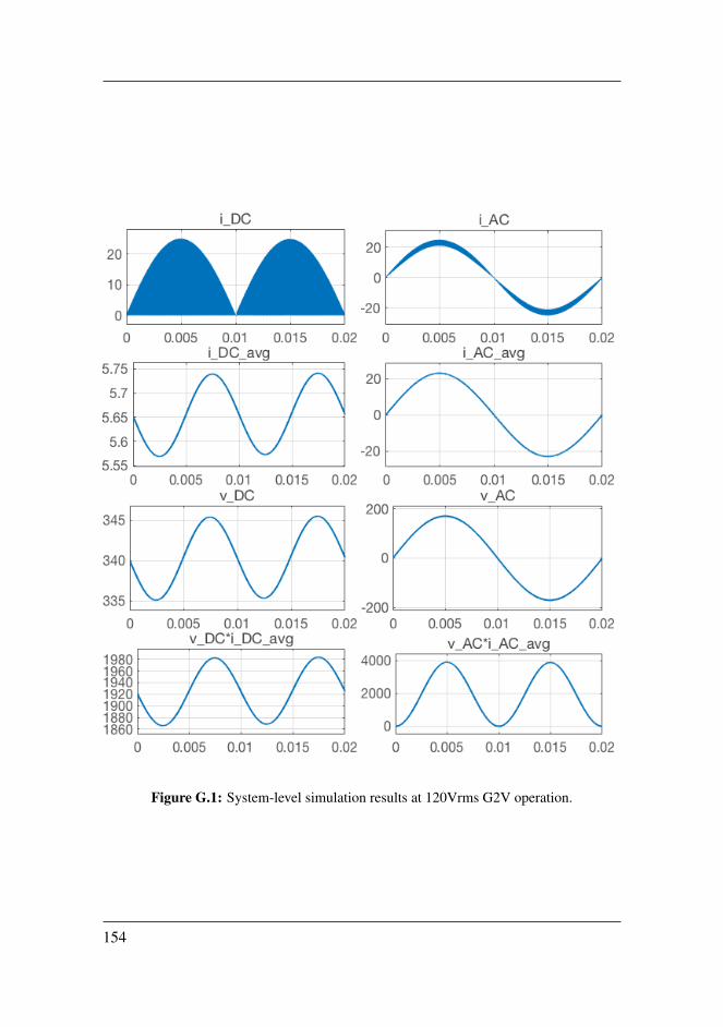
Figure G.1: System-level simulation results at 120Vrms G2V operation.
154
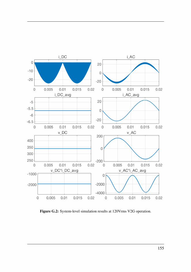
Figure G.2: System-level simulation results at 120Vrms V2G operation.
155