Embed Size (px)
Citation preview

LABORATORY MANUAL
POWER ELECTRONICS
SUBJECT CODE: 3140915
ELECTRICAL ENGINEERING DEPARTMENT
B.E. 4th SEMESTER
Amiraj College of Engineering and Technology,
Nr.Tata Nano Plant, Khoraj, Sanand, Ahmedabad.
NAME:
ENROLLMENT NO:
BATCH NO:
YEAR:

Amiraj College of Engineering and Technology, Nr.Tata Nano Plant, Khoraj, Sanand, Ahmedabad.
CERTIFICATE
This is to certify that Mr. / Ms. ______________________________________________
Of class____________________ Enrolment No ___________________________has
Satisfactorily completed the course in ____________________________________as by
the Gujarat Technological University for ____ Year (B.E.) semester___ of Electrical
Engineering in the Academic year ______.
Date of Submission:-
Faculty Name and Signature
(Subject Teacher)
Head of Department
(Electrical)

MECHANICAL ENGINEERING DEPARTMENT
B.E. 4th SEMESTER
SUBJECT: POWER ELECTRONICS
SUBJECT CODE: 3140915
List of Experiments
Sr.
No.
Title Date of
Performance
Date of
submission
Sign
Remark
1 To verify the V-I
characteristics of silicon control
rectifier (SCR)
2 To verify the UJT as a relaxation
oscillator
3 To Perform 3-phase ac power control
by TRIACS with lamp load
4 To perform the 1-phase full wave fully
controlled bridge rectifier configuration
with “R/RL load & FWD”
5 To perform the 3-Phase full wave half
controlled thyristor bridge converter
6 To simulate Single phase
half bridge inverter using
MATLAB
7 To simulate Single phase
full bridge inverter using
MATLAB
8 To generate PWM signal using
MATLAB
9 To study AC Voltage Controller
10 To study 1-phase Half wave controlled
DC motor control

POWER ELECTRONICS (3140912)
AMIRAJ COLLEGE OF ENGG & TECH Page 1
Made By: Shashant Parmar
EXPERIMENT– 1
AIM: To verify the V-I characteristics of silicon control rectifier (SCR)
APPARATUS: Experimental training kit, connecting wires.
PROCEDURE:
1. Make the connection for SCR as shown in Figure 1.
2. Keep both variable power supply knob “VAA” and “VGG” to its minimum position.
3. Switch on the kit.
4. Keep gate current Ig to zero and vary the voltage VAA from zero to maximum value in steps.
5. Note readings of VAK & IA. The SCR remains on OFF state i.e. IA remains almost zero.
6. Now set VAK to 10Vdc.
7. Now apply VGG and slowly vary the Gate current Ig. Note Ig value at which SCR turns on. As
soon as SCR turns ON, voltage across SCR “VAK” falls to a very low value i.e. approximately
0.7 to 1V.
8. Now increase VAA in steps and take the readings of VAK & IA.
9. Once SCR is in ON state, it remains in ON state only. For turning it OFF, Switch off the kit i.e.
power supply.
10. Repeat the step 5 & 6 for different values of VAK.
i.e. set VAK= 25Vdc / 50Vdc.
11. Draw the graph of voltage across SCR VAK to the corresponding anode current IA for different
value of gate current Ig.

POWER ELECTRONICS (3140912)
AMIRAJ COLLEGE OF ENGG & TECH Page 2
Made By: Shashant Parmar
DATE: / /
SIGNATURE
OBSERVATION TABLE:
Sr.
No.
Ig = 0 Ig1 = Ig2 =
Voltage
across SCR
“VAK”
Current
flowing
through SCR
“IA”
Voltage
across SCR
“VAK”
Current
flowing
through SCR
“IA”
Voltage
across SCR
“VAK”
Current
flowing
through SCR
“IA”
1 25Vdc 0 50Vdc 0
2
3
4
5
6
7
8
CONCLUSION:

POWER ELECTRONICS (3140912)
AMIRAJ COLLEGE OF ENGG & TECH Page 3
Made By: Shashant Parmar
EXPERIMENT– 2
AIM: To verify the UJT as a relaxation oscillator
APPARATUS: Experimental training kit, Connecting wires, Dual Trace CRO
PROCEDURE:
1. Select the Capacitor “C” by proper jumper wire. (0.1F, 0.22F, 0.47F or 1F)
2. Select the resistance “R” by proper jumper wire. (10K, 22 K, 33K, 47 K or 100 K)
3. Connect the one channel of CRO across the capacitor “C” and second channel of CRO across
the resistor “R1”.
4. Switch on the kit.
5. Adjust the time multiplier selector switch & voltage multiplier selector switch appropriately so
that the waveforms can be observed on the screen of DRO.
Refer Figure 1 for UJT oscillator diagram and Figure 2 for the waveform across capacitor “C” &
resistor “R1”.
6. Now vary the resistor “R” and observe the waveforms.
7. Measure the peak point voltage, valley point voltage from the capacitor voltage “Vc”. Calculate
= (Vp – Vd)/VBB.
Take Vd=0.7V and VBB=12V and Vp is to be measured from the “Vc”.
8. Measure the time period of the waveform and compare it with theoretical value of
time period T = RCln1/(1-).
9. Take the readings for the different values of resistor “R” and capacitor “C”.
10. At resistance “R” = 10K, the oscillator may or may not oscillate.

POWER ELECTRONICS (3140912)
AMIRAJ COLLEGE OF ENGG & TECH Page 4
Made By: Shashant Parmar
DATE: / /
SIGNATURE
OBSERVATION TABLE:
Capacitor “C” =
Peak point voltage Vp =
Valley point voltage Vv =
Intrinsic Standoff ratio “ ” =
Sr.
No.
Resistor “R” Measured time Period “T” Calculated Time Period “T” =
RCln1/(1- )
1.
2.
3.
4.
5.
CONCLUSION:

POWER ELECTRONICS (3140912)
AMIRAJ COLLEGE OF ENGG & TECH Page 5
Made By: Shashant Parmar
EXPERIMENT– 3
AIM: To Perform 3-phase ac power control by TRIACS with lamp load
APPARATUS: Experimental training kit, AC Voltmeter (0-240Vac), Bulb 60W – 3 Nos.
PROCEDURE:
1. For connection refer Figure.
2. Keep variable resistance “Firing angle adjustment” Potentiometer to its minimum position. i.e.
Fully anti-clockwise position.
3. Switch on the 3 Phase Power source.
4. Observe that bulb is OFF and measure AC voltage across bulb.
5. Now slowly vary the “Firing angle adjustment” Potentiometer and observe that voltage across
bulb increases and intensity of the light also increases.
6. Measure voltage across Triac and output controlled AC voltage across bulb.
7. Here, Diac is used to trigger the main Power device Triac.
8. “RC” triggering circuit is used to trigger the Diac and Diac triggers Triac.
9. By changing the value of “Firing angle adjustment” Potentiometer, the trigger (firing) angle of
the Triac is controlled, thus controlling the AC voltage across the lamp load.
10. Carefully observe following voltages on CRO one by one
a. Input Voltage, i.e. 230Vac (Phase to Neutral)
b. Voltage across load, i.e. Lamp : VL
c. Voltage across Triac : VT

POWER ELECTRONICS (3140912)
AMIRAJ COLLEGE OF ENGG & TECH Page 6
Made By: Shashant Parmar
DATE: / /
SIGNATURE
Calculations:
CONCLUSION:

POWER ELECTRONICS (3140912)
AMIRAJ COLLEGE OF ENGG & TECH Page 7
Made By: Shashant Parmar
EXPERIMENT– 4
AIM: To perform the 1-phase full wave fullycontrolled bridge rectifier configuration
with “R/RL load & FWD”
APPARATUS: Experimental training kit, Connecting wires, DC Voltmeter (0-100Vdc),
CRO Dual channel
PROCEDURE:
Part –I, With “R” load.
1. UJT synchronized triggering circuit is used to trigger the thyristors.
2. Short the Inductor “L” of 1 Henry by proper Jumper wire.
3. Keep the Firing angle adjust potentiometer i.e. variable resistor “R” to its minimum position.
4. Switch on the kit.
5. Observe the waveform in the following sequence and draw the same also.
a. Input voltage, Vin=50Vac
b. Zener voltage Vz
c. Capacitor Voltage Vc
d. Voltage across “R” Load, VRL
6. Measure the triggering angle or firing angle of the SCR by using CRO and measure the DC
voltage across the load by using DC voltmeter.
7. For changing the firing angle of the SCR, vary the potentiometer “R” and repeat the step No. 4
& 5 for different values of firing angle.
8. Switch OFF the trainer board i.e. kit.
9. Calculate the theoretical DC voltage across the load,
(VRL)dc = Vm(1+cosα)/π
Part –II, With “RL” load.
1. Remove the Short Jumper wire from the Inductor “L”.
2. Keep the Firing angle adjust potentiometer i.e. variable resistor “R” to its minimum position.

POWER ELECTRONICS (3140912)
AMIRAJ COLLEGE OF ENGG & TECH Page 8
Made By: Shashant Parmar
3. Switch on the kit.
4. Observe the waveform in the following sequence and draw the same also.
a. Input voltage, Vin=50Vac
b. Zener voltage Vz
c. Capacitor Voltage Vc
d. Voltage across “RL” Load, VRL
5. Measure the triggering angle or firing angle “α” of the SCRs and the turn off angle “β” of the
SCRs by using CRO and measure the DC voltage across the load by using DC voltmeter.
6. Because of Inductive load, the Thyristors are not able to turn off at the zero crossing but
continue to remain in conduction during the negative cycle also till current falls below the it’s
holding current value, approximately zero.
7. For changing the firing angle of the SCR, vary the potentiometer “R” and repeat the step No. 13
& 14 for different values of firing angle.
8. Switch OFF the trainer board i.e. kit.
Part –III, With “RL” load and FWD.
1. Keep the same set up as for the “RL” load but in addition connect the Free Wheeling diode
(FWD) across the load.
2. This FWD helps thyristor to turn off at the zero crossing. The stored energy free wheels through
this additional reverse biased diode connected across the “RL” load.
3. Observe the waveform in the following sequence and draw the same also.
a. Input voltage, Vin=50Vac
b. Zener voltage Vz
c. Capacitor Voltage Vc
d. Voltage across “RL” Load, VRL
4. The waveforms are same as of with “R” load. i.e. performance of the converter with “R” load is
equivalent to the converter with “RL” load & FWD.

POWER ELECTRONICS (3140912)
AMIRAJ COLLEGE OF ENGG & TECH Page 9
Made By: Shashant Parmar
DATE: / /
SIGNATURE
CALCULATIONS:
CONCLUSION:

POWER ELECTRONICS (3140912)
AMIRAJ COLLEGE OF ENGG & TECH Page 10
Made By: Shashant Parmar
EXPERIMENT– 5
Aim: To perform the 3-Phase full wave half controlled thyristor bridge converter
APPARATUS: Experimental training kit, Connecting wires, DC Voltmeter, CRO- Dual
channel
PROCEDURE:
Part – I, With “R” load.
1. Refer the circuit diagram as shown in figure.
2. Short the Inductor “L” of 1 Henry by proper Jumper wire.
3. Switch on the kit.
4. Observe the waveform in the following sequence and draw the same also.
a. Input voltage, Vin=50Vac
b. Pulses to the Thyristors
c. Voltage across “R” Load, VRL
5. For changing the firing angle of the SCR, vary the potentiometer “R” and repeat the step No. 4
for different values of firing angle.
6. Draw all above waveforms in a sequence for different value of firing angle.
7. Measure the DC voltage across the load for different firing angle.
8. Switch OFF the trainer board i.e. kit.
Part – II, With “RL” load.
1. Remove the Short Jumper wire from the Inductor “L”.
2. Switch on the kit.
3. Observe the waveform in the following sequence and draw the same also.
a. Input voltage, Vin=50Vac
b. Pulses to the Thyristors
c. Voltage across “R” Load, VRL
4. For changing the firing angle of the SCR, vary the potentiometer “R” and repeat the step No. 11
for different values of firing angle.

POWER ELECTRONICS (3140912)
AMIRAJ COLLEGE OF ENGG & TECH Page 11
Made By: Shashant Parmar
5. Draw all above waveforms in a sequence for different value of firing angle.
6. Because of Inductive load, the conducting Thyristor is not able to turn off at the zero crossing
but continue to remain in conduction during the negative cycle also till current falls below the
it’s holding current value, i.e. approximately zero. So in case of “RL” load negative voltage
appears across the load particularly when firing angle is nearer to π.
7. Measure the DC voltage across the load for different firing angle.
8. Switch OFF the trainer board i.e. kit.
Part – III, With “RL” load and FWD.
1. Keep the same set up as for the “RL” load but in addition connect the Free Wheeling diode
(FWD) across the load.
2. This FWD helps thyristor to turn off at the zero crossing. The stored energy free wheels through
this additional reverse biased diode connected across the “RL” load.
3. Observe the waveform in the following sequence and draw the same also.
d. Input voltage, Vin=50Vac
e. Pulses to the Thyristors
f. Voltage across “RL” Load with FWD, VRL
4. The waveforms are same as of with “R” load. i.e. performance of the converter with “R” load is
equivalent to the converter with “RL” load & FWD.
CALCULATIONS:

POWER ELECTRONICS (3140912)
AMIRAJ COLLEGE OF ENGG & TECH Page 12
Made By: Shashant Parmar
DATE: / /
SIGNATURE
CONCLUSION:
POWER ELECTRONICS (3140912)
AMIRAJ COLLEGE OF ENGG & TECH Page 13
Made By: Shashant Parmar
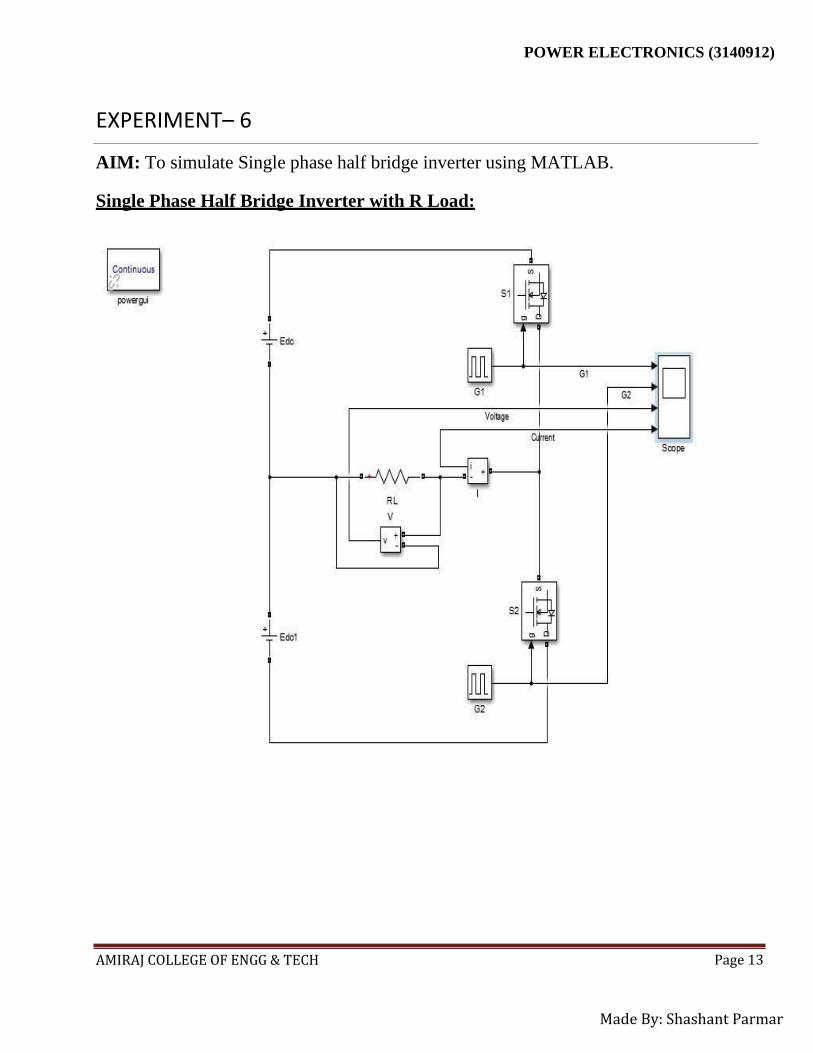
EXPERIMENT– 6
AIM: To simulate Single phase half bridge inverter using MATLAB.
Single Phase Half Bridge Inverter with R Load:

POWER ELECTRONICS (3140912)
AMIRAJ COLLEGE OF ENGG & TECH Page 14
Made By: Shashant Parmar
Waveforms:
POWER ELECTRONICS (3140912)
AMIRAJ COLLEGE OF ENGG & TECH Page 15
Made By: Shashant Parmar
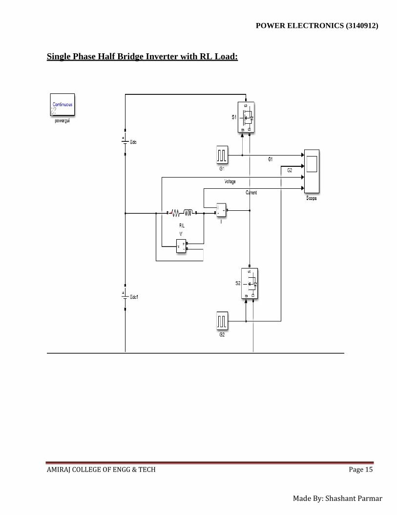
Single Phase Half Bridge Inverter with RL Load:

POWER ELECTRONICS (3140912)
AMIRAJ COLLEGE OF ENGG & TECH Page 16
Made By: Shashant Parmar
DATE: / /
SIGNATURE
Waveforms:
CONCLUSION:

POWER ELECTRONICS (3140912)
AMIRAJ COLLEGE OF ENGG & TECH Page 17
Made By: Shashant Parmar
EXPERIMENT– 7
AIM: To simulate Single phase full bridge inverter using MATLAB.
Single Phase Full Bridge Inverter with R Load:

POWER ELECTRONICS (3140912)
AMIRAJ COLLEGE OF ENGG & TECH Page 18
Made By: Shashant Parmar
Waveforms:

POWER ELECTRONICS (3140912)
AMIRAJ COLLEGE OF ENGG & TECH Page 19
Made By: Shashant Parmar
DATE: / /
SIGNATURE
CONCLUSION:

POWER ELECTRONICS (3140912)
AMIRAJ COLLEGE OF ENGG & TECH Page 20
Made By: Shashant Parmar
EXPERIMENT– 8
AIM: To generate PWM signal using MATLAB.
PROGRAM:
clc;
clear all;
t = 0:0.001:1;
fc = input('Enter the Frequency of Carrier Signal (Sawtooth) = ');
fm = input('Enter the Frequency of Message Signal (Sinusoidal) = ');
a = input('Enter the Amplitude of Carrier Signal = ');
b = input('Enter the Amplitude of Message Signal(should be < Carrier) = ');
vc = a.*sawtooth(2*pi*fc*t);
vm = b.*sin(2*pi*fm*t);
n = length(vc);
for i = 1:n
if (vm(i)>=vc(i))
pwm(i) = 1;
else
pwm(i) = 0;
end
end
% Representation of the Message Signal
subplot(3,1,1);
plot(t,vm,'black');
xlabel('Time----- >');
ylabel('Amplitude----- >');
title('Message Signal');
%legend('Message Signal ---- >');
grid on;
% Representation of the Carrier Signal
subplot(3,1,2);
plot(t,vc);
xlabel('Sample----- >');
ylabel('Amplitude----- >');
title('Carrier Signal');
%legend('Carrier Signal ---- >');
grid on;
% Representation of the PWM Signal
subplot(3,1,3);

POWER ELECTRONICS (3140912)
AMIRAJ COLLEGE OF ENGG & TECH Page 21
Made By: Shashant Parmar
plot(t,pwm,'red');
xlabel('Sample----- >');
ylabel('Amplitude----- >');
title('PWM Signal');
%legend('PWM Signal ---- >');
axis([0 1 0 2]);
grid on;
Enter the Frequency of Carrier Signal (Sawtooth) = 50
Enter the Frequency of Message Signal (Sinusoidal) = 10
Enter the Amplitude of Carrier Signal = 10
Enter the Amplitude of Message Signal(should be < Carrier) = 7
RESULTS:

POWER ELECTRONICS (3140912)
AMIRAJ COLLEGE OF ENGG & TECH Page 22
Made By: Shashant Parmar
DATE: / /
SIGNATURE
CONCLUSION:

POWER ELECTRONICS (3140912)
AMIRAJ COLLEGE OF ENGG & TECH Page 23
Made By: Shashant Parmar
EXPERIMENT– 9
AIM: - To study AC Voltage Controller.
APPARATUS:
1. Power supply
2. Performance Kit
3. Multimeter
4. Probes
5. Oscilloscope
THEORY:
AC voltage controllers (ac line voltage controllers) are employed to vary the RMS value of the
alternating voltage applied to a load circuit by introducing Thyristor between the load and a constant
voltage ac source. The RMS value of alternating voltage applied to a load circuit is controlled by
controlling the triggering angle of the Thyristor in the ac voltage controller circuits.
In brief, an ac voltage controller is a type of thyristor power converter which is used to convert a
fixed voltage, fixed frequency ac input supply to obtain a variable voltage ac output. The RMS value of
the ac output voltage and the ac power flow to the load is controlled by varying (adjusting) the trigger
angle ‘α’
There are two different types of thyristor control used in practice to control the ac power flow
• On-Off control
• Phase control

POWER ELECTRONICS (3140912)
AMIRAJ COLLEGE OF ENGG & TECH Page 24
Made By: Shashant Parmar
These are the two ac output voltage control techniques. In On-Off control technique Thyristors
are used as switches to connect the load circuit to the ac supply (source) for a fewcycles of the input ac
supply and then to disconnect it for few input cycles. The Thyristors thus act as a high speed contactor
(or high speed ac switch).
PHASE CONTROL
In phase control the Thyristors are used as switches to connect the load circuit to the input ac
supply, for a part of every input cycle. That is the ac supply voltage is chopped using Thyristors during
a part of each input cycle.
The thyristor switch is turned on for a part of every half cycle, so that input supply voltage
appears across the load and then turned off during the remaining part of input half cycle to disconnect
the ac supply from the load. (Delay angle), the output RMS voltage across the load can be
controlled.by controlling the phase angle or the trigger angle.
The trigger delay angle ‘α’ is defined as the phase angle (the value t) at which the thyristor turns
on and the load current begins to of flow. Thyristor ac voltage controllers use ac line commutation or
ac phase commutation. Thyristors in ac voltage controllers are line commutated (phase commutated)
since the input supply is ac. When the input ac voltage reverses and becomes negative during the
negative half cycle the current flowing through the conducting thyristor decreases and falls to zero.
Thus the ON thyristor naturally turns off, when the device current falls to zero.
Phase controlThyristors which are relatively inexpensive, converter grade Thyristors which are
slower than fast switching inverter grade Thyristors are normally used. For applications upto 400Hz, if
Triacs are available to meet the voltage and current ratings of a particular application, Triacs are more
commonly used.

POWER ELECTRONICS (3140912)
AMIRAJ COLLEGE OF ENGG & TECH Page 25
Made By: Shashant Parmar
CIRCUIT DIAGRAM:
OBSERVATION TABLE:
Sr.
No Supply voltage Firing Angle VO(avg)
1
2
3
4
5
6
7
8
9
10

POWER ELECTRONICS (3140912)
AMIRAJ COLLEGE OF ENGG & TECH Page 26
Made By: Shashant Parmar
DATE: / /
SIGNATURE
CONCLUSION:

POWER ELECTRONICS (3140912)
AMIRAJ COLLEGE OF ENGG & TECH Page 27
Made By: Shashant Parmar
EXPERIMENT– 10
Aim:- To study 1-phase Half wave controlled DC motor control.
Motor Configurations:
Motor power Armature voltage
:- :-
5 H.P 240 V
Speed :- 1750 RPM
Armature resistance :- 0.781 Ω Field Voltage :- 150 V
Circuit Diagram:-

AMIRAJ COLLEGE OF ENGG & TECH Page 31
POWER ELECTRONICS (3140915)
Made By: Shashant Parmar
Figure-1 For firing angle= 0

AMIRAJ COLLEGE OF ENGG & TECH Page 32
POWER ELECTRONICS (3140915)
Made By: Shashant Parmar
Figure-2 For firing angle= 30

AMIRAJ COLLEGE OF ENGG & TECH Page 33
POWER ELECTRONICS (3140915)
Made By: Shashant Parmar
Figure-3 For firing angle= 60

AMIRAJ COLLEGE OF ENGG & TECH Page 34
POWER ELECTRONICS (3140915)
Made By: Shashant Parmar
Figure-4 For firing angle= 90

AMIRAJ COLLEGE OF ENGG & TECH Page 35
POWER ELECTRONICS (3140915)
Made By: Shashant Parmar
Figure-5 For firing angle= 120

AMIRAJ COLLEGE OF ENGG & TECH Page 36
POWER ELECTRONICS (3140915)
Made By: Shashant Parmar
DATE: / /
SIGNATURE
Observation Table:
Firing Angle Speed (rad/sec)
CONCLUSION:


![ELECTRONICS AND COMMUNICATTIONS ENGINEERING · 2014-09-30 · electronics and communicattions engineering [specilisation code: 08] paper – i (choose any one subject) s.no subject](https://img.pdfslide.us/doc/110x75/5e6e0b3efae9e36ced40e513/electronics-and-communicattions-engineering-2014-09-30-electronics-and-communicattions.jpg)