Embed Size (px)
Citation preview
Power Electronics Lecture No. 14 Dr. Mohammed Tawfeeq Lazim Al-Zuhairi
1
14. DC – to – AC Converters
Single-phase inverters:
14.1 Single-phase half-bridge inverter
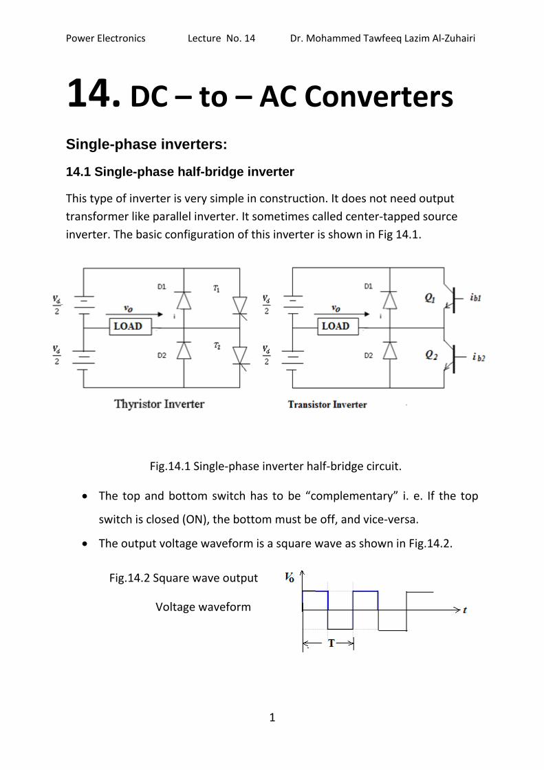
This type of inverter is very simple in construction. It does not need output
transformer like parallel inverter. It sometimes called center-tapped source
inverter. The basic configuration of this inverter is shown in Fig 14.1.
Fig.14.1 Single-phase inverter half-bridge circuit.
The top and bottom switch has to be “complementary” i. e. If the top
switch is closed (ON), the bottom must be off, and vice-versa.
The output voltage waveform is a square wave as shown in Fig.14.2.
Fig.14.2 Square wave output
Voltage waveform
Power Electronics Lecture No. 14 Dr. Mohammed Tawfeeq Lazim Al-Zuhairi
2
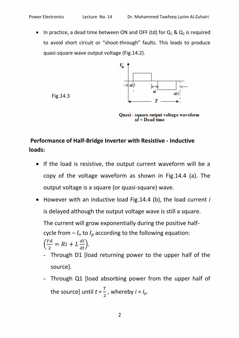
In practice, a dead time between ON and OFF (td) for Q1 & Q2 is required
to avoid short circuit or “shoot-through” faults. This leads to produce
quasi-square wave output voltage (Fig.14.2).
Fig.14.3
Performance of Half-Bridge Inverter with Resistive - Inductive
loads:
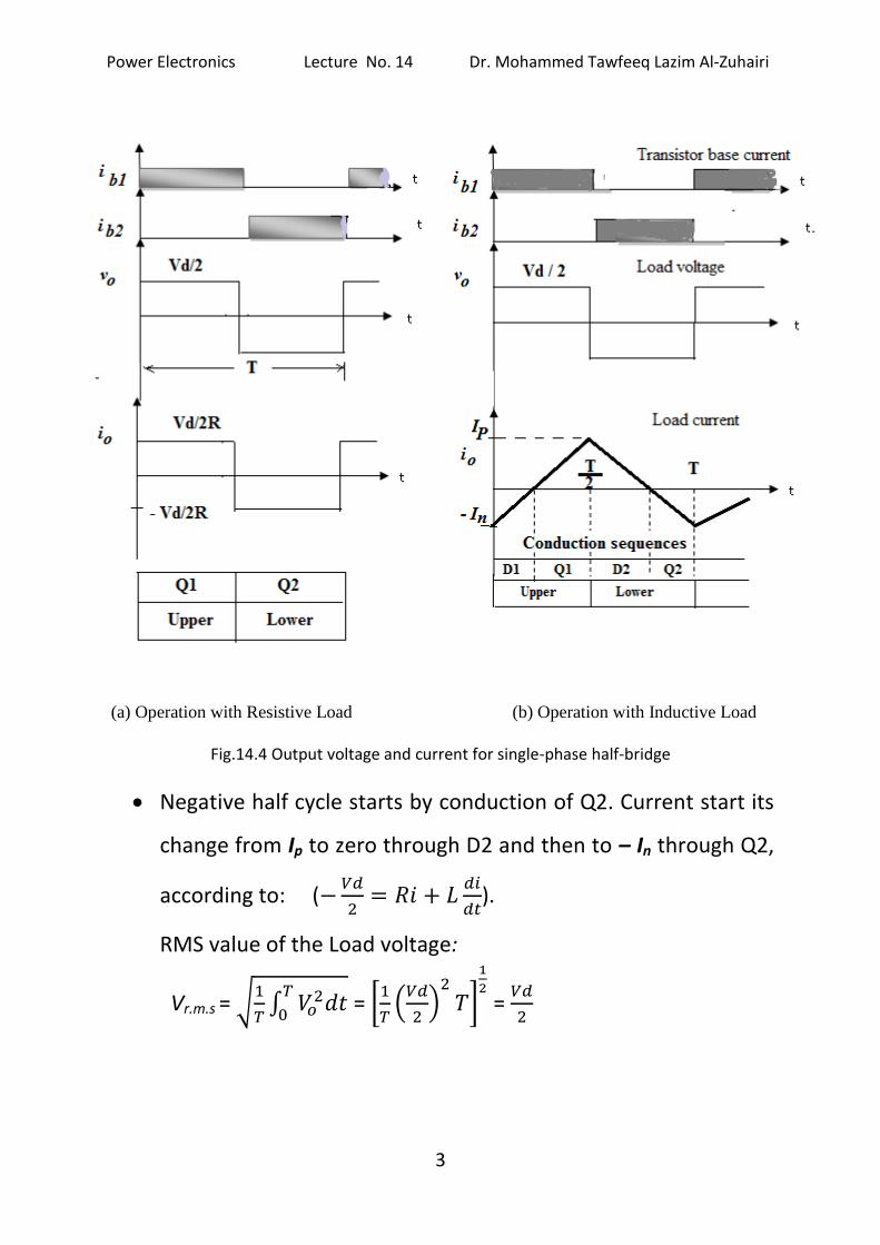
If the load is resistive, the output current waveform will be a
copy of the voltage waveform as shown in Fig.14.4 (a). The
output voltage is a square (or quasi-square) wave.
However with an inductive load Fig.14.4 (b), the load current i
is delayed although the output voltage wave is still a square.
The current will grow exponentially during the positive half-
cycle from – In to Ip according to the following equation:
- Through D1 [load returning power to the upper half of the
source].
- Through Q1 [load absorbing power from the upper half of
the source] until t =
, whereby i = Ip.
Power Electronics Lecture No. 14 Dr. Mohammed Tawfeeq Lazim Al-Zuhairi
3
(a) Operation with Resistive Load (b) Operation with Inductive Load
Fig.14.4 Output voltage and current for single-phase half-bridge
Negative half cycle starts by conduction of Q2. Current start its
change from Ip to zero through D2 and then to – In through Q2,
according to: (
).
RMS value of the Load voltage:
Vr.m.s =
=
=
Power Electronics Lecture No. 14 Dr. Mohammed Tawfeeq Lazim Al-Zuhairi
4
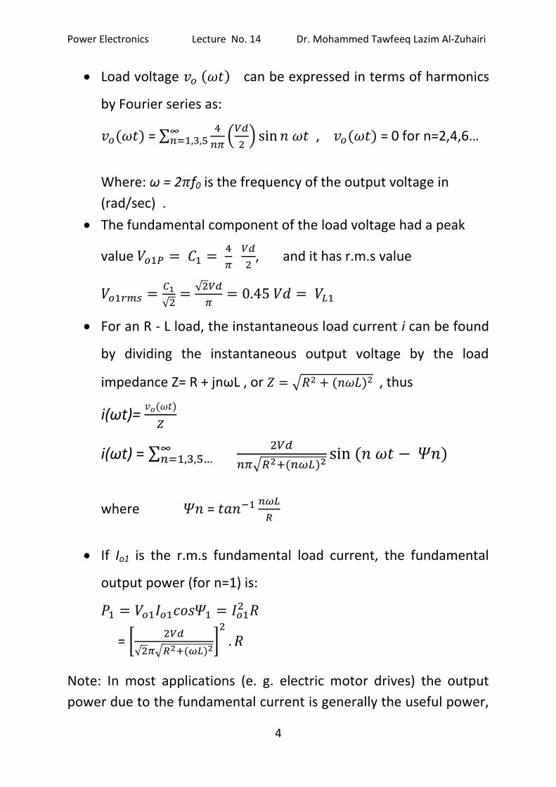
Load voltage can be expressed in terms of harmonics
by Fourier series as:
=
, = 0 for n=2,4,6…
Where: ω = 2 f0 is the frequency of the output voltage in
(rad/sec) .
The fundamental component of the load voltage had a peak
value
, and it has r.m.s value
For an R - L load, the instantaneous load current i can be found
by dividing the instantaneous output voltage by the load
impedance Z= R + jnωL , or , thus
i(ωt)=
i(ωt) =
where =
If Io1 is the r.m.s fundamental load current, the fundamental
output power (for n=1) is:
=
Note: In most applications (e. g. electric motor drives) the output
power due to the fundamental current is generally the useful power,
Power Electronics Lecture No. 14 Dr. Mohammed Tawfeeq Lazim Al-Zuhairi
5
and the power due to harmonic currents is dissipated as heat and
increases the load temperature.
Power Electronics Lecture No. 14 Dr. Mohammed Tawfeeq Lazim Al-Zuhairi
6
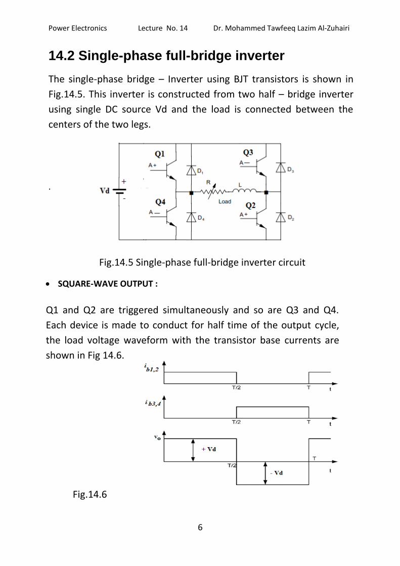
14.2 Single-phase full-bridge inverter
The single-phase bridge – Inverter using BJT transistors is shown in
Fig.14.5. This inverter is constructed from two half – bridge inverter
using single DC source Vd and the load is connected between the
centers of the two legs.
.
Fig.14.5 Single-phase full-bridge inverter circuit
SQUARE-WAVE OUTPUT :
Q1 and Q2 are triggered simultaneously and so are Q3 and Q4.
Each device is made to conduct for half time of the output cycle,
the load voltage waveform with the transistor base currents are
shown in Fig 14.6.
Fig.14.6
Power Electronics Lecture No. 14 Dr. Mohammed Tawfeeq Lazim Al-Zuhairi
7
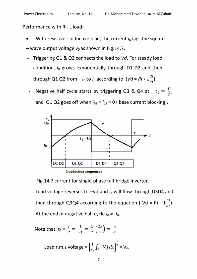
Performance with R - L load:
With resistive - inductive load, the current i0 lags the square
– wave output voltage v0 as shown in Fig.14.7.
- Triggering Q1 & Q2 connects the load to Vd. For steady load
condition, i0 grows exponentially through D1 D2 and then
through Q1 Q2 from – In to Ip according to (Vd = Ri + L
) .
- Negative half cycle starts by triggering Q3 & Q4 at
,
and Q1 Q2 goes off when ib1 = ib2 = 0 ( base current blocking).
Fig.14.7 current for single-phase full-bridge inverter.
- Load voltage reverses to –Vd and io will flow through D3D4 and
then through Q3Q4 according to the equation (-Vd = Ri + L
).
At the end of negative half cycle io = -In.
Note that: t1 =
Load r.m.s voltage =
= Vd.
Power Electronics Lecture No. 14 Dr. Mohammed Tawfeeq Lazim Al-Zuhairi
8
Load voltage V0(t) may be expressed as:
.
The peak value of the fundamental component (n=1) of the load
voltage is,
(maximum or peak value)
The RMS value of the fundamental component is
(r.m.s value).
Load r.m.s current and power can be determine from
And P =
.
where the instantaneous value of the load current io for an R-L load is
The angle by which the load current lgs the load voltage is.
.
The total harmonic distortion factor is,
THD =
Power Electronics Lecture No. 14 Dr. Mohammed Tawfeeq Lazim Al-Zuhairi
9
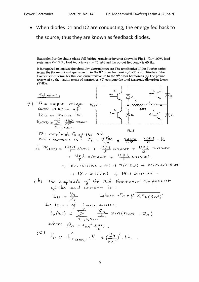
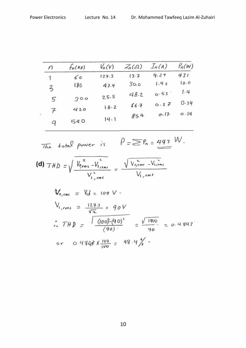
When diodes D1 and D2 are conducting, the energy fed back to
the source, thus they are known as feedback diodes.
Power Electronics Lecture No. 14 Dr. Mohammed Tawfeeq Lazim Al-Zuhairi
10
Power Electronics Lecture No. 14 Dr. Mohammed Tawfeeq Lazim Al-Zuhairi
11
!4.3 Inverter Output Voltage Control
Many inverter applications require a means of output voltage
control. In most of these applications this control is usually required
in order to provide stepless adjustment of the inverter output
voltage.
The methods of control can be group into three broad categories:-
1. Control of voltage supplies to the inverter
2. Control of voltage delivered by the inverter
3. Control of voltage within the inverter.
There are a number of well-known methods of controlling the
d.c. voltage supplies to an inverter or the a.c. voltage delivered
by an inverter. These include the use of d.c. choppers, and
phase-controlled rectifiers. The principal disadvantage of these
methods is that the power delivered by the inverter is handed
twice, once by the d.c. or a.c. voltage control and once by the
inverter.
Control of the inverter output voltage may be achieved by
incorporating time-ratio controls within the inverter circuit.
A method of controlling the voltage within an inverter involves
the use of pulse wide modulation techniques. With this
technique the inverter output voltage is controlled by varying
the duration of the output voltage pulses.
Power Electronics Lecture No. 14 Dr. Mohammed Tawfeeq Lazim Al-Zuhairi
12
Pulse width voltage and frequency control
A method of controlling the output voltage and frequency within an
inverter involves the use of pulse wide modulation techniques. With
this technique the inverter output voltage is controlled by varying
the duration of the output voltage pulses as shown in Fig.14.8.
PWM is obtained by comparing a reference signal, Ar with a
triangular carrier wave, Ac. By varying Ar from 0 to Ac , the pulse
width can be varied from 0o to 180o. The modulation index is
defined as,
Modulation Index Ac
ArM
The output voltage may be given by,
dcdcrmso VtdvV
2/1
2
2
2
2
21
The harmonic content can be reduced by using severed pulses in
each half-cycle of output voltage. The frequency of reference signal
sets the output frequency fo , and the carrier frequency fc determines
the number of pulses per half-cycle P.
o
c
f
fP
2
As M varies from 0 to 1, varies from 0 to P/ and the output
voltage from 0 to vdc .
Power Electronics Lecture No. 14 Dr. Mohammed Tawfeeq Lazim Al-Zuhairi
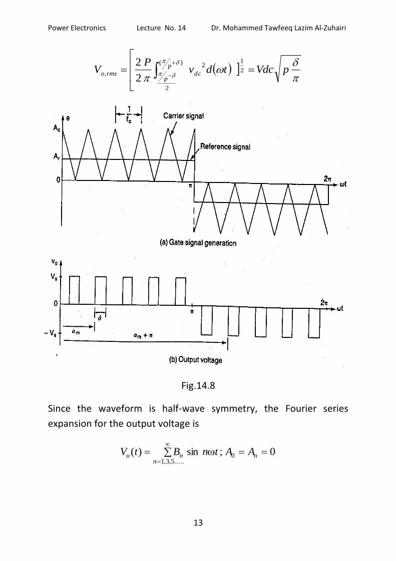
13
pVdctdvP
V dc
p
prmso
2
12)(
2
,2
2
Fig.14.8
Since the waveform is half-wave symmetry, the Fourier series
expansion for the output voltage is
.....5,3,10 0;sin)(
nnno AAtnBtV