Embed Size (px)
Citation preview

POWER ELECTRONICSHANDBOOK

Academic Press Series in EngineeringJ. David Irwin, Auburn University, Series Editor
This is a series that will include handbooks, textbooks, and professional reference books on cutting-edge areas of
engineering. Also included in this series will be single-authored professional books on state-of-the-art techniques and
methods in engineering. Its objective is to meet the needs of academic, industrial, and governmental engineers, as well as to
provide instructional material for teaching at both the undergraduate and graduate level.
The series editor, J. David Irwin, is one of the best-known engineering educators in the world. Irwin has been chairman of
the electrical engineering department at Auburn University for 27 years.
Published books in the series:
Control of Induction Motors, 2001, A. Trzynadlowski
Embedded Microcontroller Interfacing for McoR Systems, 2000, G. J. Lipovski
Soft Computing & Intelligent Systems, 2000, N. K. Sinha, M. M. Gupta
Introduction to Microcontrollers, 1999, G. J. Lipovski
Industrial Controls and Manufacturing, 1999, E. Kamen
DSP Integrated Circuits, 1999, L. Wanhammar
Time Domain Electromagnetics, 1999, S. M. Rao
Single- and Multi-Chip Microcontroller Interfacing, 1999, G. J. Lipovski
Control in Robotics and Automation, 1999, B. K. Ghosh, N. Xi, and T. J. Tarn
POWER ELECTRONICSHANDBOOK
EDITOR-IN-CHIEF
MUHAMMAD H. RASHIDPh.D., Fellow IEE, Fellow IEEEProfessor and DirectorUniversity of Florida=University of West Florida Joint Program and Computer EngineeringUniversity of West FloridaPensacola, Florida
SAN DIEGO = SAN FRANCISCO = NEW YORK = BOSTON = LONDON = SYDNEY = TOKYO

This book is printed on acid-free paper.
Copyright # 2001 by ACADEMIC PRESS
All rights reserved.
No part of this publication may be reproduced or transmitted in any form or by
any means, electronic or mechanical, including photocopy, recording, or any information
storage and retrieval system, without permission in writing from the publisher.
Requests for permission to make copies of any part of the work should be mailed to:
Permissions Department, Harcourt, Inc., 6277 Sea Harbor Drive, Orlando, Florida
32887-6777.
Explicit permission from Academic Press is not required to reproduce a maximum of
two figures or tables from an Academic Press chapter in another scientific or research
publication provided that the material has not been credited to another source and that
full credit to the Academic Press chapter is given.
ACADEMIC PRESS
A Harcourt Science and Technology Company
525 B Street, Suite 1900, San Diego, California 92101-4495, USA
http:==www.academicpress.com
Academic Press
Harcourt Place, 32 Jamestown Road, London NW1 7BY, UK
http:==www.academicpress.com
Library of Congress Catalog Card Number: 00-2001088199
International Standard Book Number: 0-12-581650-2
Printed in Canada
01 02 03 04 05 06 FR 9 8 7 6 5 4 3 2 1

Contents
Preface . . . . . . . . . . . . . . . . . . . . . . . . . . . . . . . . . . . . . . . . . . . . . . . . . . . . . . . . . . . . . . . . . . . . . . . . . . . . xi
List of Contributors . . . . . . . . . . . . . . . . . . . . . . . . . . . . . . . . . . . . . . . . . . . . . . . . . . . . . . . . . . . . . . . . . . . xiii
1 Introduction Philip Krein . . . . . . . . . . . . . . . . . . . . . . . . . . . . . . . . . . . . . . . . . . . . . . . . . . . . . . . . . . 1
1.1 Power Electronics Defined. . . . . . . . . . . . . . . . . . . . . . . . . . . . . . . . . . . . . . . . . . . . . . . . . . . . . . . . 1
1.2 Key Characteristics. . . . . . . . . . . . . . . . . . . . . . . . . . . . . . . . . . . . . . . . . . . . . . . . . . . . . . . . . . . . . 2
1.3 Trends in Power Supplies . . . . . . . . . . . . . . . . . . . . . . . . . . . . . . . . . . . . . . . . . . . . . . . . . . . . . . . . 3
1.4 Conversion Examples . . . . . . . . . . . . . . . . . . . . . . . . . . . . . . . . . . . . . . . . . . . . . . . . . . . . . . . . . . . 4
1.5 Tools For Analysis and Design . . . . . . . . . . . . . . . . . . . . . . . . . . . . . . . . . . . . . . . . . . . . . . . . . . . . . 7
1.6 Summary . . . . . . . . . . . . . . . . . . . . . . . . . . . . . . . . . . . . . . . . . . . . . . . . . . . . . . . . . . . . . . . . . . . 12
2 The Power Diode Ali I. Maswood . . . . . . . . . . . . . . . . . . . . . . . . . . . . . . . . . . . . . . . . . . . . . . . . . . . . . 15
2.1 Diode as a Switch . . . . . . . . . . . . . . . . . . . . . . . . . . . . . . . . . . . . . . . . . . . . . . . . . . . . . . . . . . . . . 15
2.2 Some Properties of PN Junction . . . . . . . . . . . . . . . . . . . . . . . . . . . . . . . . . . . . . . . . . . . . . . . . . . . 15
2.3 Common Diode Types . . . . . . . . . . . . . . . . . . . . . . . . . . . . . . . . . . . . . . . . . . . . . . . . . . . . . . . . . . 17
2.4 Typical Diode Ratings . . . . . . . . . . . . . . . . . . . . . . . . . . . . . . . . . . . . . . . . . . . . . . . . . . . . . . . . . . 17
2.5 Snubber Circuits for Diode . . . . . . . . . . . . . . . . . . . . . . . . . . . . . . . . . . . . . . . . . . . . . . . . . . . . . . . 19
2.6 Series and Parallel Connection of Power Diodes . . . . . . . . . . . . . . . . . . . . . . . . . . . . . . . . . . . . . . . . . 19
2.7 Typical Applications of Diodes . . . . . . . . . . . . . . . . . . . . . . . . . . . . . . . . . . . . . . . . . . . . . . . . . . . . 23
2.8 Standard Datasheet for Diode Selection . . . . . . . . . . . . . . . . . . . . . . . . . . . . . . . . . . . . . . . . . . . . . . 23
3 Thyristors Jerry Hudgins, Enrico Santi, Antonio Caiafa, Katherine Lengel, and Patrick R. Palmer . . . . . . . . . . . 27
3.1 Introduction . . . . . . . . . . . . . . . . . . . . . . . . . . . . . . . . . . . . . . . . . . . . . . . . . . . . . . . . . . . . . . . . . 27
3.2 Basic Structure and Operation . . . . . . . . . . . . . . . . . . . . . . . . . . . . . . . . . . . . . . . . . . . . . . . . . . . . . 28
3.3 Static Characteristics . . . . . . . . . . . . . . . . . . . . . . . . . . . . . . . . . . . . . . . . . . . . . . . . . . . . . . . . . . . 30
3.4 Dynamic Switching Characteristics . . . . . . . . . . . . . . . . . . . . . . . . . . . . . . . . . . . . . . . . . . . . . . . . . . 33
3.5 Thyristor Parameters . . . . . . . . . . . . . . . . . . . . . . . . . . . . . . . . . . . . . . . . . . . . . . . . . . . . . . . . . . . 37
3.6 Types of Thyristors . . . . . . . . . . . . . . . . . . . . . . . . . . . . . . . . . . . . . . . . . . . . . . . . . . . . . . . . . . . . 38
3.7 Gate Drive Requirements . . . . . . . . . . . . . . . . . . . . . . . . . . . . . . . . . . . . . . . . . . . . . . . . . . . . . . . . 45
3.8 PSpice Model . . . . . . . . . . . . . . . . . . . . . . . . . . . . . . . . . . . . . . . . . . . . . . . . . . . . . . . . . . . . . . . . 47
3.9 Applications . . . . . . . . . . . . . . . . . . . . . . . . . . . . . . . . . . . . . . . . . . . . . . . . . . . . . . . . . . . . . . . . . 50
4 Gate Turn-Off Thyristors Muhammad H. Rashid . . . . . . . . . . . . . . . . . . . . . . . . . . . . . . . . . . . . . . . . . . 55
4.1 Introduction . . . . . . . . . . . . . . . . . . . . . . . . . . . . . . . . . . . . . . . . . . . . . . . . . . . . . . . . . . . . . . . . . 55
4.2 Basic Structure and Operation . . . . . . . . . . . . . . . . . . . . . . . . . . . . . . . . . . . . . . . . . . . . . . . . . . . . . 55
4.3 GTO Thyristor Models . . . . . . . . . . . . . . . . . . . . . . . . . . . . . . . . . . . . . . . . . . . . . . . . . . . . . . . . . . 57
4.4 Static Characteristics . . . . . . . . . . . . . . . . . . . . . . . . . . . . . . . . . . . . . . . . . . . . . . . . . . . . . . . . . . . 57
4.5 Switching Phases . . . . . . . . . . . . . . . . . . . . . . . . . . . . . . . . . . . . . . . . . . . . . . . . . . . . . . . . . . . . . . 59
4.6 SPICE GTO Model . . . . . . . . . . . . . . . . . . . . . . . . . . . . . . . . . . . . . . . . . . . . . . . . . . . . . . . . . . . . 60
4.7 Applications . . . . . . . . . . . . . . . . . . . . . . . . . . . . . . . . . . . . . . . . . . . . . . . . . . . . . . . . . . . . . . . . . 61
v

5 Power Bipolar Transistors Marcelo Godoy Simoes . . . . . . . . . . . . . . . . . . . . . . . . . . . . . . . . . . . . . . . . . . . 63
5.1 Introduction . . . . . . . . . . . . . . . . . . . . . . . . . . . . . . . . . . . . . . . . . . . . . . . . . . . . . . . . . . . . . . . . . 63
5.2 Basic Structure and Operation . . . . . . . . . . . . . . . . . . . . . . . . . . . . . . . . . . . . . . . . . . . . . . . . . . . . . 64
5.3 Static Characteristics . . . . . . . . . . . . . . . . . . . . . . . . . . . . . . . . . . . . . . . . . . . . . . . . . . . . . . . . . . . . 65
5.4 Dynamic Switching Characteristics . . . . . . . . . . . . . . . . . . . . . . . . . . . . . . . . . . . . . . . . . . . . . . . . . . 68
5.5 Transistor Base Drive Applications. . . . . . . . . . . . . . . . . . . . . . . . . . . . . . . . . . . . . . . . . . . . . . . . . . . 69
5.6 SPICE Simulation of Bipolar Junction Transistors . . . . . . . . . . . . . . . . . . . . . . . . . . . . . . . . . . . . . . . . 71
5.7 BJT Applications . . . . . . . . . . . . . . . . . . . . . . . . . . . . . . . . . . . . . . . . . . . . . . . . . . . . . . . . . . . . . . . 72
6 The Power MOSFET Issa Batarseh . . . . . . . . . . . . . . . . . . . . . . . . . . . . . . . . . . . . . . . . . . . . . . . . . . . . . 75
6.1 Introduction . . . . . . . . . . . . . . . . . . . . . . . . . . . . . . . . . . . . . . . . . . . . . . . . . . . . . . . . . . . . . . . . . 75
6.2 The Need for Switching in Power Electronic Circuits . . . . . . . . . . . . . . . . . . . . . . . . . . . . . . . . . . . . . . 76
6.3 General Switching Characteristics . . . . . . . . . . . . . . . . . . . . . . . . . . . . . . . . . . . . . . . . . . . . . . . . . . . 78
6.4 The Power MOSFET . . . . . . . . . . . . . . . . . . . . . . . . . . . . . . . . . . . . . . . . . . . . . . . . . . . . . . . . . . . . 80
6.5 MOSFET Structure . . . . . . . . . . . . . . . . . . . . . . . . . . . . . . . . . . . . . . . . . . . . . . . . . . . . . . . . . . . . . 81
6.6 MOSFET Regions of Operation. . . . . . . . . . . . . . . . . . . . . . . . . . . . . . . . . . . . . . . . . . . . . . . . . . . . . 83
6.7 MOSFET PSPICE Model . . . . . . . . . . . . . . . . . . . . . . . . . . . . . . . . . . . . . . . . . . . . . . . . . . . . . . . . . 93
6.8 Comparison of Power Devices . . . . . . . . . . . . . . . . . . . . . . . . . . . . . . . . . . . . . . . . . . . . . . . . . . . . . 96
6.9 Future Trends in Power Devices . . . . . . . . . . . . . . . . . . . . . . . . . . . . . . . . . . . . . . . . . . . . . . . . . . . . 98
7 Insulated Gate Bipolar Transistor S. Abedinpour and K. Shenai . . . . . . . . . . . . . . . . . . . . . . . . . . . . . . . . . 101
7.1 Introduction . . . . . . . . . . . . . . . . . . . . . . . . . . . . . . . . . . . . . . . . . . . . . . . . . . . . . . . . . . . . . . . . . 101
7.2 Basic Structure and Operation . . . . . . . . . . . . . . . . . . . . . . . . . . . . . . . . . . . . . . . . . . . . . . . . . . . . . 102
7.3 Static Characteristics . . . . . . . . . . . . . . . . . . . . . . . . . . . . . . . . . . . . . . . . . . . . . . . . . . . . . . . . . . . . 104
7.4 Dynamic Switching Characteristics . . . . . . . . . . . . . . . . . . . . . . . . . . . . . . . . . . . . . . . . . . . . . . . . . . 105
7.5 IGBT Performance Parameters . . . . . . . . . . . . . . . . . . . . . . . . . . . . . . . . . . . . . . . . . . . . . . . . . . . . . 107
7.6 Gate-Drive Requirements . . . . . . . . . . . . . . . . . . . . . . . . . . . . . . . . . . . . . . . . . . . . . . . . . . . . . . . . . 109
7.7 Circuit Models . . . . . . . . . . . . . . . . . . . . . . . . . . . . . . . . . . . . . . . . . . . . . . . . . . . . . . . . . . . . . . . . 111
7.8 Applications . . . . . . . . . . . . . . . . . . . . . . . . . . . . . . . . . . . . . . . . . . . . . . . . . . . . . . . . . . . . . . . . . . 113
8 MOS Controlled Thyristors (MCTs) S. Yuvarajan . . . . . . . . . . . . . . . . . . . . . . . . . . . . . . . . . . . . . . . . . . 117
8.1 Introduction . . . . . . . . . . . . . . . . . . . . . . . . . . . . . . . . . . . . . . . . . . . . . . . . . . . . . . . . . . . . . . . . . 117
8.2 Equivalent Circuit and Switching Characteristics . . . . . . . . . . . . . . . . . . . . . . . . . . . . . . . . . . . . . . . . . 118
8.3 Comparison of MCT and Other Power Devices . . . . . . . . . . . . . . . . . . . . . . . . . . . . . . . . . . . . . . . . . . 119
8.4 Gate Drive for MCTs. . . . . . . . . . . . . . . . . . . . . . . . . . . . . . . . . . . . . . . . . . . . . . . . . . . . . . . . . . . . 120
8.5 Protection of MCTs. . . . . . . . . . . . . . . . . . . . . . . . . . . . . . . . . . . . . . . . . . . . . . . . . . . . . . . . . . . . . 120
8.6 Simulation Model of an MCT. . . . . . . . . . . . . . . . . . . . . . . . . . . . . . . . . . . . . . . . . . . . . . . . . . . . . . 121
8.7 Generation-1 and Generation-2 MCTs . . . . . . . . . . . . . . . . . . . . . . . . . . . . . . . . . . . . . . . . . . . . . . . . 121
8.8 N-channel MCT . . . . . . . . . . . . . . . . . . . . . . . . . . . . . . . . . . . . . . . . . . . . . . . . . . . . . . . . . . . . . . . 121
8.9 Base Resistance-Controlled Thyristor [14]. . . . . . . . . . . . . . . . . . . . . . . . . . . . . . . . . . . . . . . . . . . . . . 121
8.10 MOS Turn-Off Thyristor [15] . . . . . . . . . . . . . . . . . . . . . . . . . . . . . . . . . . . . . . . . . . . . . . . . . . . . . . 122
8.11 Applications of PMCT . . . . . . . . . . . . . . . . . . . . . . . . . . . . . . . . . . . . . . . . . . . . . . . . . . . . . . . . . . . 122
8.12 Conclusions . . . . . . . . . . . . . . . . . . . . . . . . . . . . . . . . . . . . . . . . . . . . . . . . . . . . . . . . . . . . . . . . . . 124
8.13 Appendix. . . . . . . . . . . . . . . . . . . . . . . . . . . . . . . . . . . . . . . . . . . . . . . . . . . . . . . . . . . . . . . . . . . . 124
9 Static Induction Devices Bogdan M. Wilamowski . . . . . . . . . . . . . . . . . . . . . . . . . . . . . . . . . . . . . . . . . . . 127
9.1 Introduction . . . . . . . . . . . . . . . . . . . . . . . . . . . . . . . . . . . . . . . . . . . . . . . . . . . . . . . . . . . . . . . . . 127
9.2 Theory of Static Induction Devices . . . . . . . . . . . . . . . . . . . . . . . . . . . . . . . . . . . . . . . . . . . . . . . . . . 127
9.3 Characteristics of Static Induction Transistor. . . . . . . . . . . . . . . . . . . . . . . . . . . . . . . . . . . . . . . . . . . . 128
9.4 Bipolar Mode Operation of SI Devices (BSIT). . . . . . . . . . . . . . . . . . . . . . . . . . . . . . . . . . . . . . . . . . . 130
9.5 Emitters for Static Induction Devices . . . . . . . . . . . . . . . . . . . . . . . . . . . . . . . . . . . . . . . . . . . . . . . . . 130
9.6 Static Induction Diode (SID) . . . . . . . . . . . . . . . . . . . . . . . . . . . . . . . . . . . . . . . . . . . . . . . . . . . . . . 131
9.7 Lateral Punch-Through Transistor (LPTT) . . . . . . . . . . . . . . . . . . . . . . . . . . . . . . . . . . . . . . . . . . . . . 132
9.8 Static Induction Transistor Logic (SITL). . . . . . . . . . . . . . . . . . . . . . . . . . . . . . . . . . . . . . . . . . . . . . . 132
9.9 BJT Saturation Protected by SIT . . . . . . . . . . . . . . . . . . . . . . . . . . . . . . . . . . . . . . . . . . . . . . . . . . . . 132
9.10 Static Induction MOS Transistor (SIMOS) . . . . . . . . . . . . . . . . . . . . . . . . . . . . . . . . . . . . . . . . . . . . . 133
vi Contents
9.11 Space-Charge Limiting Load (SCLL). . . . . . . . . . . . . . . . . . . . . . . . . . . . . . . . . . . . . . . . . . . . . . . . . 134
9.12 Power MOS Transistors . . . . . . . . . . . . . . . . . . . . . . . . . . . . . . . . . . . . . . . . . . . . . . . . . . . . . . . . . 134
9.13 Static Induction Thyristor . . . . . . . . . . . . . . . . . . . . . . . . . . . . . . . . . . . . . . . . . . . . . . . . . . . . . . . . 135
9.14 Gate Turn-Off Thyristor (GTO) . . . . . . . . . . . . . . . . . . . . . . . . . . . . . . . . . . . . . . . . . . . . . . . . . . . . 136
10 Diode Rectifiers Yim-Shu Lee and Martin H. L. Chow . . . . . . . . . . . . . . . . . . . . . . . . . . . . . . . . . . . . . . . 139
10.1 Introduction . . . . . . . . . . . . . . . . . . . . . . . . . . . . . . . . . . . . . . . . . . . . . . . . . . . . . . . . . . . . . . . . 139
10.2 Single-Phase Diode Rectifiers . . . . . . . . . . . . . . . . . . . . . . . . . . . . . . . . . . . . . . . . . . . . . . . . . . . . . 139
10.3 Three-Phase Diode Rectifiers . . . . . . . . . . . . . . . . . . . . . . . . . . . . . . . . . . . . . . . . . . . . . . . . . . . . . 144
10.4 Poly-Phase Diode Rectifiers . . . . . . . . . . . . . . . . . . . . . . . . . . . . . . . . . . . . . . . . . . . . . . . . . . . . . . 148
10.5 Filtering Systems in Rectifier Circuits . . . . . . . . . . . . . . . . . . . . . . . . . . . . . . . . . . . . . . . . . . . . . . . 150
10.6 High-Frequency Diode Rectifier Circuits . . . . . . . . . . . . . . . . . . . . . . . . . . . . . . . . . . . . . . . . . . . . . 154
11 Single-Phase Controlled Rectifiers Jose Rodrıguez and Alejandro Weinstein . . . . . . . . . . . . . . . . . . . . . . . . . 169
11.1 Line Commutated Single-Phase Controlled Rectifiers. . . . . . . . . . . . . . . . . . . . . . . . . . . . . . . . . . . . . 169
11.2 Unity Power Factor Single-Phase Rectifiers. . . . . . . . . . . . . . . . . . . . . . . . . . . . . . . . . . . . . . . . . . . . 175
12 Three-Phase Controlled Rectifiers Juan W. Dixon. . . . . . . . . . . . . . . . . . . . . . . . . . . . . . . . . . . . . . . . . . 183
12.1 Introduction . . . . . . . . . . . . . . . . . . . . . . . . . . . . . . . . . . . . . . . . . . . . . . . . . . . . . . . . . . . . . . . . 183
12.2 Line-Commutated Controlled Rectifiers. . . . . . . . . . . . . . . . . . . . . . . . . . . . . . . . . . . . . . . . . . . . . . 183
12.3 Force-Commutated Three-Phase Controlled Rectifiers . . . . . . . . . . . . . . . . . . . . . . . . . . . . . . . . . . . . 196
13 DC-DC Converters Dariusz Czarkowski . . . . . . . . . . . . . . . . . . . . . . . . . . . . . . . . . . . . . . . . . . . . . . . . . 211
13.1 Introduction . . . . . . . . . . . . . . . . . . . . . . . . . . . . . . . . . . . . . . . . . . . . . . . . . . . . . . . . . . . . . . . . 211
13.2 DC Choppers . . . . . . . . . . . . . . . . . . . . . . . . . . . . . . . . . . . . . . . . . . . . . . . . . . . . . . . . . . . . . . . 212
13.3 Step-Down (Buck) Converter. . . . . . . . . . . . . . . . . . . . . . . . . . . . . . . . . . . . . . . . . . . . . . . . . . . . . 213
13.4 Step-Up (Boost) Converter . . . . . . . . . . . . . . . . . . . . . . . . . . . . . . . . . . . . . . . . . . . . . . . . . . . . . . 215
13.5 Buck-Boost Converter. . . . . . . . . . . . . . . . . . . . . . . . . . . . . . . . . . . . . . . . . . . . . . . . . . . . . . . . . . 216
13.6 Cuk Converter. . . . . . . . . . . . . . . . . . . . . . . . . . . . . . . . . . . . . . . . . . . . . . . . . . . . . . . . . . . . . . . 218
13.7 Effects of Parasitics. . . . . . . . . . . . . . . . . . . . . . . . . . . . . . . . . . . . . . . . . . . . . . . . . . . . . . . . . . . . 218
13.8 Synchronous and Bidirectional Converters . . . . . . . . . . . . . . . . . . . . . . . . . . . . . . . . . . . . . . . . . . . . 220
13.9 Control Principles . . . . . . . . . . . . . . . . . . . . . . . . . . . . . . . . . . . . . . . . . . . . . . . . . . . . . . . . . . . . 221
13.10 Applications of DC-DC Converters . . . . . . . . . . . . . . . . . . . . . . . . . . . . . . . . . . . . . . . . . . . . . . . . . 223
14 Inverters Jose R. Espinoza . . . . . . . . . . . . . . . . . . . . . . . . . . . . . . . . . . . . . . . . . . . . . . . . . . . . . . . . . . 225
14.1 Introduction . . . . . . . . . . . . . . . . . . . . . . . . . . . . . . . . . . . . . . . . . . . . . . . . . . . . . . . . . . . . . . . . 225
14.2 Single-Phase Voltage Source Inverters . . . . . . . . . . . . . . . . . . . . . . . . . . . . . . . . . . . . . . . . . . . . . . . 227
14.3 Three-Phase Voltage Source Inverters . . . . . . . . . . . . . . . . . . . . . . . . . . . . . . . . . . . . . . . . . . . . . . . 235
14.4 Current Source Inverters . . . . . . . . . . . . . . . . . . . . . . . . . . . . . . . . . . . . . . . . . . . . . . . . . . . . . . . . 241
14.5 Closed-Loop Operation of Inverters . . . . . . . . . . . . . . . . . . . . . . . . . . . . . . . . . . . . . . . . . . . . . . . . 250
14.6 Regeneration in Inverters . . . . . . . . . . . . . . . . . . . . . . . . . . . . . . . . . . . . . . . . . . . . . . . . . . . . . . . 256
14.7 Multistage Inverters . . . . . . . . . . . . . . . . . . . . . . . . . . . . . . . . . . . . . . . . . . . . . . . . . . . . . . . . . . . 260
14.8 Acknowledgments . . . . . . . . . . . . . . . . . . . . . . . . . . . . . . . . . . . . . . . . . . . . . . . . . . . . . . . . . . . . 267
15 Resonant and Soft-Switching Converters S. Y. (Ron) Hui and Henry S. H. Chung. . . . . . . . . . . . . . . . . . . . 271
15.1 Introduction . . . . . . . . . . . . . . . . . . . . . . . . . . . . . . . . . . . . . . . . . . . . . . . . . . . . . . . . . . . . . . . . 271
15.2 Classification . . . . . . . . . . . . . . . . . . . . . . . . . . . . . . . . . . . . . . . . . . . . . . . . . . . . . . . . . . . . . . . . 272
15.3 Resonant Switch . . . . . . . . . . . . . . . . . . . . . . . . . . . . . . . . . . . . . . . . . . . . . . . . . . . . . . . . . . . . . 272
15.4 Quasi-Resonant Converters . . . . . . . . . . . . . . . . . . . . . . . . . . . . . . . . . . . . . . . . . . . . . . . . . . . . . . 273
15.5 ZVS in High-Frequency Applications . . . . . . . . . . . . . . . . . . . . . . . . . . . . . . . . . . . . . . . . . . . . . . . 275
15.6 Multiresonant Converters (MRC) . . . . . . . . . . . . . . . . . . . . . . . . . . . . . . . . . . . . . . . . . . . . . . . . . . 280
15.7 Zero-Voltage-Transition (ZVT) Converters. . . . . . . . . . . . . . . . . . . . . . . . . . . . . . . . . . . . . . . . . . . . 282
15.8 Nondissipative Active Clamp Network. . . . . . . . . . . . . . . . . . . . . . . . . . . . . . . . . . . . . . . . . . . . . . . 283
15.9 Load Resonant Converters . . . . . . . . . . . . . . . . . . . . . . . . . . . . . . . . . . . . . . . . . . . . . . . . . . . . . . . 284
15.10 Control Circuits for Resonant Converters . . . . . . . . . . . . . . . . . . . . . . . . . . . . . . . . . . . . . . . . . . . . 287
15.11 Extended-Period Quasi-Resonant (EP-QR) Converters . . . . . . . . . . . . . . . . . . . . . . . . . . . . . . . . . . . . 289
15.12 Soft-Switching and EMI Suppression. . . . . . . . . . . . . . . . . . . . . . . . . . . . . . . . . . . . . . . . . . . . . . . . 293
15.13 Snubbers and Soft-Switching for High Power Devices . . . . . . . . . . . . . . . . . . . . . . . . . . . . . . . . . . . . 293
Contents vii

15.14 Soft-Switching DC-AC Power Inverters . . . . . . . . . . . . . . . . . . . . . . . . . . . . . . . . . . . . . . . . . . . . . . . 294
16 AC-AC Converters Ajit K. Chattopadhyay . . . . . . . . . . . . . . . . . . . . . . . . . . . . . . . . . . . . . . . . . . . . . . . . 307
16.1 Introduction . . . . . . . . . . . . . . . . . . . . . . . . . . . . . . . . . . . . . . . . . . . . . . . . . . . . . . . . . . . . . . . . . 307
16.2 Single-Phase AC=AC Voltage Controller . . . . . . . . . . . . . . . . . . . . . . . . . . . . . . . . . . . . . . . . . . . . . . 307
16.3 Three-Phase AC=AC Voltage Controllers . . . . . . . . . . . . . . . . . . . . . . . . . . . . . . . . . . . . . . . . . . . . . . 312
16.4 Cycloconverters . . . . . . . . . . . . . . . . . . . . . . . . . . . . . . . . . . . . . . . . . . . . . . . . . . . . . . . . . . . . . . . 316
16.5 Matrix Converter. . . . . . . . . . . . . . . . . . . . . . . . . . . . . . . . . . . . . . . . . . . . . . . . . . . . . . . . . . . . . . 327
16.6 Applications of AC=AC Converters. . . . . . . . . . . . . . . . . . . . . . . . . . . . . . . . . . . . . . . . . . . . . . . . . . 331
17 DC=DC Conversion Technique and Nine Series LUO-Converters Fang Lin Luo, Hong Ye,
and Muhammad H. Rashid . . . . . . . . . . . . . . . . . . . . . . . . . . . . . . . . . . . . . . . . . . . . . . . . . . . . . . . . . . . 335
17.1 Introduction . . . . . . . . . . . . . . . . . . . . . . . . . . . . . . . . . . . . . . . . . . . . . . . . . . . . . . . . . . . . . . . . . 335
17.2 Positive Ouput Luo-Converters . . . . . . . . . . . . . . . . . . . . . . . . . . . . . . . . . . . . . . . . . . . . . . . . . . . . 337
17.3 Negative Ouput Luo-Converters . . . . . . . . . . . . . . . . . . . . . . . . . . . . . . . . . . . . . . . . . . . . . . . . . . . 353
17.4 Double Output Luo-Converters . . . . . . . . . . . . . . . . . . . . . . . . . . . . . . . . . . . . . . . . . . . . . . . . . . . . 359
17.5 Multiple-Quadrant Operating Luo-Converters . . . . . . . . . . . . . . . . . . . . . . . . . . . . . . . . . . . . . . . . . . 372
17.6 Switched-Capacitor Multiquadrant Luo-Converters. . . . . . . . . . . . . . . . . . . . . . . . . . . . . . . . . . . . . . . 377
17.7 Switched-Inductor Multiquadrant Luo-Converters . . . . . . . . . . . . . . . . . . . . . . . . . . . . . . . . . . . . . . . 386
17.8 Multiquadrant ZCS Quasi-Resonant Luo-Converters. . . . . . . . . . . . . . . . . . . . . . . . . . . . . . . . . . . . . . 390
17.9 Multiquadrant ZVS Quasi-Resonant Luo-Converters. . . . . . . . . . . . . . . . . . . . . . . . . . . . . . . . . . . . . . 394
17.10 Synchronous Rectifier DC=DC Luo-Converters . . . . . . . . . . . . . . . . . . . . . . . . . . . . . . . . . . . . . . . . . 397
17.11 Gate Control, Luo-Resonator . . . . . . . . . . . . . . . . . . . . . . . . . . . . . . . . . . . . . . . . . . . . . . . . . . . . . 401
17.12 Applications . . . . . . . . . . . . . . . . . . . . . . . . . . . . . . . . . . . . . . . . . . . . . . . . . . . . . . . . . . . . . . . . . 402
18 Gate Drive Circuits M. Syed J. Asghar . . . . . . . . . . . . . . . . . . . . . . . . . . . . . . . . . . . . . . . . . . . . . . . . . . 407
18.1 Introduction . . . . . . . . . . . . . . . . . . . . . . . . . . . . . . . . . . . . . . . . . . . . . . . . . . . . . . . . . . . . . . . . . 407
18.2 Thyristor Gate Requirements. . . . . . . . . . . . . . . . . . . . . . . . . . . . . . . . . . . . . . . . . . . . . . . . . . . . . . 407
18.3 Trigger Circuits for Thyristors . . . . . . . . . . . . . . . . . . . . . . . . . . . . . . . . . . . . . . . . . . . . . . . . . . . . . 409
18.4 Simple Gate Trigger Circuits for Thyristors . . . . . . . . . . . . . . . . . . . . . . . . . . . . . . . . . . . . . . . . . . . . 410
18.5 Drivers for Gate Commutation Switches . . . . . . . . . . . . . . . . . . . . . . . . . . . . . . . . . . . . . . . . . . . . . . 422
18.6 Some Practical Driver Circuits. . . . . . . . . . . . . . . . . . . . . . . . . . . . . . . . . . . . . . . . . . . . . . . . . . . . . 427
19 Control Methods for Power Converters J. Fernando Silva . . . . . . . . . . . . . . . . . . . . . . . . . . . . . . . . . . . . . 431
19.1 Introduction . . . . . . . . . . . . . . . . . . . . . . . . . . . . . . . . . . . . . . . . . . . . . . . . . . . . . . . . . . . . . . . . . 431
19.2 Power Converter Control using State-Space Averaged Models. . . . . . . . . . . . . . . . . . . . . . . . . . . . . . . . 432
19.3 Sliding-Mode Control of Power Converters . . . . . . . . . . . . . . . . . . . . . . . . . . . . . . . . . . . . . . . . . . . . 450
19.4 Fuzzy Logic Control of Power Converters . . . . . . . . . . . . . . . . . . . . . . . . . . . . . . . . . . . . . . . . . . . . . 481
19.5 Conclusions . . . . . . . . . . . . . . . . . . . . . . . . . . . . . . . . . . . . . . . . . . . . . . . . . . . . . . . . . . . . . . . . . 484
20 Power Supplies Y. M. Lai . . . . . . . . . . . . . . . . . . . . . . . . . . . . . . . . . . . . . . . . . . . . . . . . . . . . . . . . . . . 487
20.1 Introduction . . . . . . . . . . . . . . . . . . . . . . . . . . . . . . . . . . . . . . . . . . . . . . . . . . . . . . . . . . . . . . . . . 487
20.2 Linear Series Voltage Regulator . . . . . . . . . . . . . . . . . . . . . . . . . . . . . . . . . . . . . . . . . . . . . . . . . . . . 488
20.3 Linear Shunt Voltage Regulator . . . . . . . . . . . . . . . . . . . . . . . . . . . . . . . . . . . . . . . . . . . . . . . . . . . . 491
20.4 Integrated Circuit Voltage Regulators . . . . . . . . . . . . . . . . . . . . . . . . . . . . . . . . . . . . . . . . . . . . . . . . 492
20.5 Switching Regulators . . . . . . . . . . . . . . . . . . . . . . . . . . . . . . . . . . . . . . . . . . . . . . . . . . . . . . . . . . . 494
21 Electronic Ballasts J. Marcos Alonso . . . . . . . . . . . . . . . . . . . . . . . . . . . . . . . . . . . . . . . . . . . . . . . . . . . . 507
21.1 Introduction . . . . . . . . . . . . . . . . . . . . . . . . . . . . . . . . . . . . . . . . . . . . . . . . . . . . . . . . . . . . . . . . . 507
21.2 High-Frequency Supply of Discharge Lamps . . . . . . . . . . . . . . . . . . . . . . . . . . . . . . . . . . . . . . . . . . . 513
21.3 Discharge Lamp Modeling . . . . . . . . . . . . . . . . . . . . . . . . . . . . . . . . . . . . . . . . . . . . . . . . . . . . . . . 516
21.4 Resonant Inverters for Electronic Ballasts . . . . . . . . . . . . . . . . . . . . . . . . . . . . . . . . . . . . . . . . . . . . . 519
21.5 High-Power-Factor Electronic Ballasts . . . . . . . . . . . . . . . . . . . . . . . . . . . . . . . . . . . . . . . . . . . . . . . 527
21.6 Applications . . . . . . . . . . . . . . . . . . . . . . . . . . . . . . . . . . . . . . . . . . . . . . . . . . . . . . . . . . . . . . . . . 529
22 Power Electronics in Capacitor Charging Applications R. Mark Nelms. . . . . . . . . . . . . . . . . . . . . . . . . . . . 533
22.1 Introduction . . . . . . . . . . . . . . . . . . . . . . . . . . . . . . . . . . . . . . . . . . . . . . . . . . . . . . . . . . . . . . . . . 533
22.2 High-Voltage dc Power Supply with Charging Resistor . . . . . . . . . . . . . . . . . . . . . . . . . . . . . . . . . . . . 533
viii Contents
22.3 Resonance Charging . . . . . . . . . . . . . . . . . . . . . . . . . . . . . . . . . . . . . . . . . . . . . . . . . . . . . . . . . . . 534
22.4 Switching Converters . . . . . . . . . . . . . . . . . . . . . . . . . . . . . . . . . . . . . . . . . . . . . . . . . . . . . . . . . . 535
23 Power Electronics for Renewable Energy Sources C. V. Nayar, S. M. Islam, and Hari Sharma . . . . . . . . . . . 539
23.1 Introduction . . . . . . . . . . . . . . . . . . . . . . . . . . . . . . . . . . . . . . . . . . . . . . . . . . . . . . . . . . . . . . . . 539
23.2 Power Electronics for Photovoltaic Power Systems . . . . . . . . . . . . . . . . . . . . . . . . . . . . . . . . . . . . . . 540
23.3 Power Electronics for Wind Power Systems . . . . . . . . . . . . . . . . . . . . . . . . . . . . . . . . . . . . . . . . . . . 562
24 HVDC Transmission Vijay K. Sood . . . . . . . . . . . . . . . . . . . . . . . . . . . . . . . . . . . . . . . . . . . . . . . . . . . . 575
24.1 Introduction . . . . . . . . . . . . . . . . . . . . . . . . . . . . . . . . . . . . . . . . . . . . . . . . . . . . . . . . . . . . . . . . 575
24.2 Main Components of HVDC Converter Station . . . . . . . . . . . . . . . . . . . . . . . . . . . . . . . . . . . . . . . . 580
24.3 Analysis of Converter Bridges . . . . . . . . . . . . . . . . . . . . . . . . . . . . . . . . . . . . . . . . . . . . . . . . . . . . 583
24.4 Controls and Protection . . . . . . . . . . . . . . . . . . . . . . . . . . . . . . . . . . . . . . . . . . . . . . . . . . . . . . . . 583
24.5 MTDC Operation . . . . . . . . . . . . . . . . . . . . . . . . . . . . . . . . . . . . . . . . . . . . . . . . . . . . . . . . . . . . 589
24.6 Applications . . . . . . . . . . . . . . . . . . . . . . . . . . . . . . . . . . . . . . . . . . . . . . . . . . . . . . . . . . . . . . . . 591
24.7 Modern Trends . . . . . . . . . . . . . . . . . . . . . . . . . . . . . . . . . . . . . . . . . . . . . . . . . . . . . . . . . . . . . . 592
24.8 DC System Simulation Techniques . . . . . . . . . . . . . . . . . . . . . . . . . . . . . . . . . . . . . . . . . . . . . . . . . 595
24.9 Conclusion . . . . . . . . . . . . . . . . . . . . . . . . . . . . . . . . . . . . . . . . . . . . . . . . . . . . . . . . . . . . . . . . . 596
25 Multilevel Converters and VAR Compensation Azeddine Draou, Mustapha Benghanem, and Ali Tahri . . . . . . 599
25.1 Introduction . . . . . . . . . . . . . . . . . . . . . . . . . . . . . . . . . . . . . . . . . . . . . . . . . . . . . . . . . . . . . . . . 599
25.2 Reactive Power Phenomena and Their Compensation . . . . . . . . . . . . . . . . . . . . . . . . . . . . . . . . . . . . 600
25.3 Modeling and Analysis of an Advanced Static VAR Compensator . . . . . . . . . . . . . . . . . . . . . . . . . . . . 603
25.4 Static VAR Compensator for the Improvement of Stability of a Turbo Alternator . . . . . . . . . . . . . . . . . 612
25.5 Multilevel Inverters. . . . . . . . . . . . . . . . . . . . . . . . . . . . . . . . . . . . . . . . . . . . . . . . . . . . . . . . . . . . 615
25.6 The Harmonics Elimination Method for a Three-Level Inverter . . . . . . . . . . . . . . . . . . . . . . . . . . . . . 619
25.7 Three-Level ASVC Structure Connected to the Network. . . . . . . . . . . . . . . . . . . . . . . . . . . . . . . . . . . 622
26 Drive Types and Specifications Yahya Shakweh . . . . . . . . . . . . . . . . . . . . . . . . . . . . . . . . . . . . . . . . . . . 629
26.1 Overview . . . . . . . . . . . . . . . . . . . . . . . . . . . . . . . . . . . . . . . . . . . . . . . . . . . . . . . . . . . . . . . . . . 629
26.2 Drive Requirements and Specifications . . . . . . . . . . . . . . . . . . . . . . . . . . . . . . . . . . . . . . . . . . . . . . 633
26.3 Drive Classifications and Characteristics . . . . . . . . . . . . . . . . . . . . . . . . . . . . . . . . . . . . . . . . . . . . . 636
26.4 Load Profiles and Characteristics . . . . . . . . . . . . . . . . . . . . . . . . . . . . . . . . . . . . . . . . . . . . . . . . . . 641
26.5 Variable-Speed Drive Topologies. . . . . . . . . . . . . . . . . . . . . . . . . . . . . . . . . . . . . . . . . . . . . . . . . . . 644
26.6 PWM VSI Drive . . . . . . . . . . . . . . . . . . . . . . . . . . . . . . . . . . . . . . . . . . . . . . . . . . . . . . . . . . . . . 650
26.7 Applications . . . . . . . . . . . . . . . . . . . . . . . . . . . . . . . . . . . . . . . . . . . . . . . . . . . . . . . . . . . . . . . . 657
26.8 Summary . . . . . . . . . . . . . . . . . . . . . . . . . . . . . . . . . . . . . . . . . . . . . . . . . . . . . . . . . . . . . . . . . . 660
27 Motor Drives M. F. Rahman, D. Patterson, A. Cheok, and R. Betts . . . . . . . . . . . . . . . . . . . . . . . . . . . . . . . 663
27.1 Introduction . . . . . . . . . . . . . . . . . . . . . . . . . . . . . . . . . . . . . . . . . . . . . . . . . . . . . . . . . . . . . . . . 664
27.2 DC Motor Drives. . . . . . . . . . . . . . . . . . . . . . . . . . . . . . . . . . . . . . . . . . . . . . . . . . . . . . . . . . . . . 665
27.3 Induction Motor Drives . . . . . . . . . . . . . . . . . . . . . . . . . . . . . . . . . . . . . . . . . . . . . . . . . . . . . . . . 670
27.4 Synchronous Motor Drives . . . . . . . . . . . . . . . . . . . . . . . . . . . . . . . . . . . . . . . . . . . . . . . . . . . . . . 681
27.5 Permanent Magnet ac Synchronous Motor Drives . . . . . . . . . . . . . . . . . . . . . . . . . . . . . . . . . . . . . . . 689
27.6 Permanent-Magnet Brushless dc (BLDC) Motor Drives . . . . . . . . . . . . . . . . . . . . . . . . . . . . . . . . . . . 694
27.7 Servo Drives . . . . . . . . . . . . . . . . . . . . . . . . . . . . . . . . . . . . . . . . . . . . . . . . . . . . . . . . . . . . . . . . 704
27.8 Stepper Motor Drives . . . . . . . . . . . . . . . . . . . . . . . . . . . . . . . . . . . . . . . . . . . . . . . . . . . . . . . . . . 710
27.9 Switched-Reluctance Motor Drives . . . . . . . . . . . . . . . . . . . . . . . . . . . . . . . . . . . . . . . . . . . . . . . . . 717
27.10 Synchronous Reluctance Motor Drives . . . . . . . . . . . . . . . . . . . . . . . . . . . . . . . . . . . . . . . . . . . . . . 727
28 Sensorless Vector and Direct-Torque-Controlled Drives Peter Vas and Pekka Tiitinen . . . . . . . . . . . . . . . . .
28.1 General . . . . . . . . . . . . . . . . . . . . . . . . . . . . . . . . . . . . . . . . . . . . . . . . . . . . . . . . . . . . . . . . . . . 735
28.2 Basic Types of Torque-Controlled Drive Schemes: Vector Drives, Direct-Torque-Controlled Drives . . . . . . 736
28.3 Motion Control DSPS by Texas Instruments . . . . . . . . . . . . . . . . . . . . . . . . . . . . . . . . . . . . . . . . . . 766
29 Artificial-Intelligence-Based Drives Peter Vas. . . . . . . . . . . . . . . . . . . . . . . . . . . . . . . . . . . . . . . . . . . . . 769
29.1 General Aspects of the Application of AI-Based Techniques . . . . . . . . . . . . . . . . . . . . . . . . . . . . . . . . 769
29.2 AI-Based Techniques. . . . . . . . . . . . . . . . . . . . . . . . . . . . . . . . . . . . . . . . . . . . . . . . . . . . . . . . . . . 770
Contents ix

29.3 AI Applications in Electrical Machines and Drives . . . . . . . . . . . . . . . . . . . . . . . . . . . . . . . . . . . . . . . 773
29.4 Industrial Applications of AI in Drives by Hitachi, Yaskawa, Texas Instruments and SGS Thomson . . . . . . 774
29.5 Application of Neural-Network-Based Speed Estimators . . . . . . . . . . . . . . . . . . . . . . . . . . . . . . . . . . . 774
30 Fuzzy Logic in Electric Drives Ahmed Rubaai . . . . . . . . . . . . . . . . . . . . . . . . . . . . . . . . . . . . . . . . . . . . . 779
30.1 Introduction . . . . . . . . . . . . . . . . . . . . . . . . . . . . . . . . . . . . . . . . . . . . . . . . . . . . . . . . . . . . . . . . . 779
30.2 The Fuzzy Logic Concept . . . . . . . . . . . . . . . . . . . . . . . . . . . . . . . . . . . . . . . . . . . . . . . . . . . . . . . . 779
30.3 Applications of Fuzzy Logic to Electric Drives . . . . . . . . . . . . . . . . . . . . . . . . . . . . . . . . . . . . . . . . . . 784
30.4 Hardware System Description . . . . . . . . . . . . . . . . . . . . . . . . . . . . . . . . . . . . . . . . . . . . . . . . . . . . . 788
30.5 Conclusion. . . . . . . . . . . . . . . . . . . . . . . . . . . . . . . . . . . . . . . . . . . . . . . . . . . . . . . . . . . . . . . . . . 789
31 Automotive Applications of Power Electronics David J. Perreault, Khurram K. Afridi, and Iftikhar A. Khan . . . 791
31.1 Introduction . . . . . . . . . . . . . . . . . . . . . . . . . . . . . . . . . . . . . . . . . . . . . . . . . . . . . . . . . . . . . . . . . 791
31.2 The Present Automotive Electrical Power System . . . . . . . . . . . . . . . . . . . . . . . . . . . . . . . . . . . . . . . . 792
31.3 System Environment . . . . . . . . . . . . . . . . . . . . . . . . . . . . . . . . . . . . . . . . . . . . . . . . . . . . . . . . . . . 792
31.4 Functions Enabled by Power Electronics . . . . . . . . . . . . . . . . . . . . . . . . . . . . . . . . . . . . . . . . . . . . . . 797
31.5 Multiplexed Load Control. . . . . . . . . . . . . . . . . . . . . . . . . . . . . . . . . . . . . . . . . . . . . . . . . . . . . . . . 801
31.6 Electromechanical Power Conversion . . . . . . . . . . . . . . . . . . . . . . . . . . . . . . . . . . . . . . . . . . . . . . . . 803
31.7 Dual=High-Voltage Automotive Electrical System . . . . . . . . . . . . . . . . . . . . . . . . . . . . . . . . . . . . . . . . 808
31.8 Electric and Hybrid Electric Vehicles . . . . . . . . . . . . . . . . . . . . . . . . . . . . . . . . . . . . . . . . . . . . . . . . 812
31.9 Summary . . . . . . . . . . . . . . . . . . . . . . . . . . . . . . . . . . . . . . . . . . . . . . . . . . . . . . . . . . . . . . . . . . . 813
32 Power Quality S. Mark Halpin and Angela Card. . . . . . . . . . . . . . . . . . . . . . . . . . . . . . . . . . . . . . . . . . . . 817
32.1 Introduction . . . . . . . . . . . . . . . . . . . . . . . . . . . . . . . . . . . . . . . . . . . . . . . . . . . . . . . . . . . . . . . . . 817
32.2 Power Quality. . . . . . . . . . . . . . . . . . . . . . . . . . . . . . . . . . . . . . . . . . . . . . . . . . . . . . . . . . . . . . . . 818
32.3 Reactive Power and Harmonic Compensation . . . . . . . . . . . . . . . . . . . . . . . . . . . . . . . . . . . . . . . . . . 823
32.4 IEEE Standards . . . . . . . . . . . . . . . . . . . . . . . . . . . . . . . . . . . . . . . . . . . . . . . . . . . . . . . . . . . . . . . 827
32.5 Conclusions . . . . . . . . . . . . . . . . . . . . . . . . . . . . . . . . . . . . . . . . . . . . . . . . . . . . . . . . . . . . . . . . . 828
33 Active Filters Luis Moran and Juan Dixon . . . . . . . . . . . . . . . . . . . . . . . . . . . . . . . . . . . . . . . . . . . . . . . . 829
33.1 Introduction . . . . . . . . . . . . . . . . . . . . . . . . . . . . . . . . . . . . . . . . . . . . . . . . . . . . . . . . . . . . . . . . . 829
33.2 Types of Active Power Filters. . . . . . . . . . . . . . . . . . . . . . . . . . . . . . . . . . . . . . . . . . . . . . . . . . . . . . 829
33.3 Shunt Active Power Filters . . . . . . . . . . . . . . . . . . . . . . . . . . . . . . . . . . . . . . . . . . . . . . . . . . . . . . . 830
33.4 Series Active Power Filters . . . . . . . . . . . . . . . . . . . . . . . . . . . . . . . . . . . . . . . . . . . . . . . . . . . . . . . 841
34 Computer Simulation of Power Electronics and Motor Drives Michael Giesselmann . . . . . . . . . . . . . . . . . . 853
34.1 Introduction . . . . . . . . . . . . . . . . . . . . . . . . . . . . . . . . . . . . . . . . . . . . . . . . . . . . . . . . . . . . . . . . . 853
34.2 Use of Simulation Tools for Design and Analysis . . . . . . . . . . . . . . . . . . . . . . . . . . . . . . . . . . . . . . . . 853
34.3 Simulation of Power Electronics Circuits with PSpice1 . . . . . . . . . . . . . . . . . . . . . . . . . . . . . . . . . . . . 854
34.4 Simulations of Power Electronic Circuits and Electric Machines . . . . . . . . . . . . . . . . . . . . . . . . . . . . . . 857
34.5 Simulations of ac Induction Machines using Field Oriented (Vector) Control. . . . . . . . . . . . . . . . . . . . . 860
34.6 Simulation of Sensorless Vector Control Using PSpice1 Release 9. . . . . . . . . . . . . . . . . . . . . . . . . . . . . 863
34.7 Simulations Using Simplorer1 . . . . . . . . . . . . . . . . . . . . . . . . . . . . . . . . . . . . . . . . . . . . . . . . . . . . 868
34.8 Conclusions . . . . . . . . . . . . . . . . . . . . . . . . . . . . . . . . . . . . . . . . . . . . . . . . . . . . . . . . . . . . . . . . . 870
35 Packaging and Smart Power Systems Douglas C. Hopkins . . . . . . . . . . . . . . . . . . . . . . . . . . . . . . . . . . . . . 871
35.1 Introduction . . . . . . . . . . . . . . . . . . . . . . . . . . . . . . . . . . . . . . . . . . . . . . . . . . . . . . . . . . . . . . . . . 871
35.2 Background . . . . . . . . . . . . . . . . . . . . . . . . . . . . . . . . . . . . . . . . . . . . . . . . . . . . . . . . . . . . . . . . . 871
35.3 Functional Integration . . . . . . . . . . . . . . . . . . . . . . . . . . . . . . . . . . . . . . . . . . . . . . . . . . . . . . . . . . 872
35.4 Assessing Partitioning Technologies . . . . . . . . . . . . . . . . . . . . . . . . . . . . . . . . . . . . . . . . . . . . . . . . . 874
35.5 Full-Cost Model [5]. . . . . . . . . . . . . . . . . . . . . . . . . . . . . . . . . . . . . . . . . . . . . . . . . . . . . . . . . . . . 877
35.6 Partitioning Approach . . . . . . . . . . . . . . . . . . . . . . . . . . . . . . . . . . . . . . . . . . . . . . . . . . . . . . . . . . 878
35.7 Example 2.2 kW Motor Drive Design . . . . . . . . . . . . . . . . . . . . . . . . . . . . . . . . . . . . . . . . . . . . . . . . 879
35.8 Acknowledgment . . . . . . . . . . . . . . . . . . . . . . . . . . . . . . . . . . . . . . . . . . . . . . . . . . . . . . . . . . . . . . 881
Index . . . . . . . . . . . . . . . . . . . . . . . . . . . . . . . . . . . . . . . . . . . . . . . . . . . . . . . . . . . . . . . . . . . . . . . . . . . . . 883
x Contents
Preface
Introduction
The purpose of Power Electronics Handbook is to provide a
reference that is both concise and useful for engineering
students and practicing professionals. It is designed to cover
a wide range of topics that make up the field of power
electronics in a well-organized and highly informative
manner. The Handbook is a careful blend of both traditional
topics and new advancements. Special emphasis is placed on
practical applications, thus, this Handbook is not a theoretical
one, but an enlightening presentation of the usefulness of the
rapidly growing field of power electronics. The presentation is
tutorial in nature in order to enhance the value of the book to
the reader and foster a clear understanding of the material.
The contributors to this Handbook span the globe, with
fifty-four authors from twelve different countries, some of
whom are the leading authorities in their areas of expertise. All
were chosen because of their intimate knowledge of their
subjects, and their contributions make this a comprehensive
state-of-the-art guide to the expanding field of power electro-
nics and its applications covering:
� the characteristics of modern power semiconductor
devices, which are used as switches to perform the
power conversions from ac-dc, dc-dc, dc-ac, and ac-ac;
� both the fundamental principles and in-depth study of
the operation, analysis, and design of various power
converters; and
� examples of recent applications of power electronics.
Power Electronics Backgrounds
The first electronics revolution began in 1948 with the inven-
tion of the silicon transistor at Bell Telephone Laboratories by
Bardeen, Bratain, and Schockley. Most of today’s advanced
electronic technologies are traceable to that invention, and
modern microelectronics has evolved over the years from these
silicon semiconductors. The second electronics revolution
began with the development of a commercial thyristor by
the General Electric Company in 1958. That was the beginning
of a new era of power electronics. Since then, many different
types of power semiconductor devices and conversion tech-
niques have been introduced.
The demand for energy, particularly in electrical forms, is
ever-increasing in order to improve the standard of living.
Power electronics helps with the efficient use of electricity,
thereby reducing power consumption. Semiconductor devices
are used as switches for power conversion or processing, as are
solid state electronics for efficient control of the amount of
power and energy flow. Higher efficiency and lower losses are
sought for devices for a range of applications, from microwave
ovens to high-voltage dc transmission. New devices and power
electronic systems are now evolving for even more effective
control of power and energy.
Power electronics has already found an important place in
modern technology and has revolutionized control of power
and energy. As the voltage and current ratings and switching
characteristics of power semiconductor devices keep improv-
ing, the range of applications continues to expand in areas
such as lamp controls, power supplies to motion control,
factory automation, transportation, energy storage, multi-
megawatt industrial drives, and electric power transmission
and distribution. The greater efficiency and tighter control
features of power electronics are becoming attractive for
applications in motion control by replacing the earlier
electro-mechanical and electronic systems. Applications in
power transmission include high-voltage dc (VHDC) conver-
ter stations, flexible ac transmission system (FACTS), and
static-var compensators. In power distribution these include
dc-to-ac conversion, dynamic filters, frequency conversion,
and Custom Power System.
Almost all new electrical or electromechanical equipment,
from household air conditioners and computer power supplies
to industrial motor controls, contain power electronic circuits
xi

and=or systems. In order to keep up, working engineers
involved in control and conversion of power and energy
into applications ranging from several hundred voltages at a
fraction of an ampere for display devices to about 10,000 V at
high-voltage dc transmission, should have a working knowl-
edge of power electronics.
Organization
The Handbook starts with an introductory chapter and moves
on to cover topics on power semiconductor devices, power
converters, applications and peripheral issues. The book is
organized into six areas, the first of which includes chapters on
operation and characterizations of power semiconductor
devices: power diode, thyristor, gate turn-off thyristor
(GTO), power bipolar transistor (BJT), power MOSFET,
insulated gate bipolar transistor, MOS controlled thyristor
(MCT), and static induction devices.
The next topic area includes chapters covering various types
of power converters, the principles of operation and the
methods for the analysis and design of power converters.
This also includes gate drive circuits and control methods
for power converters. The next three chapters cover applica-
tions in power supplies, electronics ballasts, renewable energy
sources, HVDC transmission, VAR compensation, and capa-
citor charging.
The following six chapters focus on the operation, theory
and control methods of motor drives, and automotive
systems. We then move on to two chapters on power quality
issues and active filters, and two chapters on computer
simulation, packaging and smart power systems.
Locating Your Topic
A table of contents is presented at the front of the book, and
each chapter begins with its own table of contents. The reader
should look over these tables of contents to become familiar
with the structure, organization, and content of the book.
Audience
The Handbook is designed to provide both students and
practicing engineers with answers to questions involving the
wide spectrum of power electronics. The book can be used
as a textbook for graduate students in electrical or systems
engineering, or as a reference book for senior undergraduate
students and for engineers who are interested and involved in
operation, project management, design, and analysis of power
electronics equipment and motor drives.
Acknowledgments
This Handbook was made possible through the expertise
and dedication of outstanding authors from throughout the
world. I gratefully acknowledge the personnel at Academic
Press who produced the book, including Jane Phelan. In
addition, special thanks are due to Joel D. Claypool, the
executive editor for this book.
Finally, I express my deep appreciation to my wife, Fatema
Rashid, who graciously puts up with my publication activities.
Muhammad H. Rashid, Editor-in-Chief
xii Preface

List of Contributors
Chapter 1
Philip Krein
Department of Electrical and Computer Engineering
University of Illinois at Urbana–Champaign
341 William L. Everitt Laboratory
1406 West Green Street
Urbana, Illinois 61801
USA
Chapter 2
Ali I. Maswood
School of EEE
Nanyang Technological University
Nanyang Avenue
Singapore 639798
Chapter 3
Jerry Hudgins, Enrico Santi, Antonio Caiafa, Katherine Lengel
Department of Electrical Engineering
University of South Carolina
Columbia, South Carolina 29208
USA
Patrick R. Palmer
Department of Engineering
Cambridge University
Trumpington Street
Cambridge CB2 1PZ
UK
Chapter 4
Muhammad H. Rashid
Electrical and Computer Engineering
University of West Florida
11000 University Parkway
Pensacola, Florida 32514-5754
USA
Chapter 5
Marcelo Godoy Simoes
Engineering Division
Colorado School of Mines
Golden, Colorado 80401-1887
USA
Chapter 6
Issa Batarseh
College of Engineering and Computer Science
University of Central Florida
Orlando, Florida 32816
USA
Chapter 7
S. Abedinpour
Department of Electrical Engineering and Computer Science
University of Illinois at Chicago
Chicago, Illinois 60607
USA
K. Shenai
851 South Morgan Street (M=C 154)
Chicago, Illinois 60607-7053
USA
Chapter 8
S. Yuvarajan
Department of Electrical Engineering
North Dakota State University
P.O. Box 5285
Fargo, North Dakota 58105-5285
USA
Chapter 9
B. M. Wilamowski
College of Engineering
University of Idaho
Boise, ID 83712
USA
xiii

Chapter 10
Yim Shu Lee, Martin H. L. Chow
Department of Electronic and Information Engineering
The Hong Kong Polytechnic University
Hung Hom
Hong Kong
Chapter 11
Jose Rodrıguez, Alejandro Weinstein
Department of Electronics
Universidad Tecnica
Federico, Santa Maria
Valparaıso
Chile
Chapter 12
Juan W. Dixon
Department of Electrical Engineering
Catholic University of Chile
Vicuna Mackenna 4860
Santiago
Chile
Chapter 13
Dariusz Czarkowski
Department of Electrical and Computer Engineering
Polytechnic University
Six Metrotech Center
Brooklyn, New York 11201
USA
Chapter 14
Jose R. Espinoza
Depto. Ing. Electrica, Of. 220
Universidad de Concepcion
Casilla 160-C, Correo 3
Concepcion
Chile
Chapter 15
S. Y. (Ron) Hui, Henry S. H. Chung
Department of Electronic Engineering
City University of Hong Kong
Tat Chee Avenue
Kowloon
Hong Kong
Chapter 16
Ajit K. Chattopadhyay
Electrical Engineering Department
Bengal Engineering College
Howrah-711 103
India
Chapter 17
Fang Lin Luo, Hong Ye
School of Electrical and Electronic Engineering
Block S2
Nanyang Technological University
Nanyang Avenue
Singapore 639798
Muhammad H. Rashid
Electrical and Computer Engineering
University of West Florida
11000 University Parkway
Pensacola, Florida 32514-5754
USA
Chapter 18
M. Syed J. Asghar
Department of Electrical Engineering
Aligarh Muslim University
Aligarh
India
Chapter 19
J. Fernando Silva
Instituto Superior Tecnico
CAUTL, DEEC
Maquinas Electricas e Electronica de Potencia (24)
Technical University of Lisbon
Av. Rovisco Pais 1, 1049-001
Lisboa
Portugal
Chapter 20
Y. M. Lai
Department of Electronic and Information Engineering
The Hong Kong Polytechnic University
Hung Hom
Hong Kong
Chapter 21
J. Marcos Alonso
University of Oveido
DIEECS – Tecnologia Electronica
Campus de Viesques s=n
Edificio de Electronica
33204 Gijon
Spain
Chapter 22
R. Mark Nelms
Department of Electrical and Computer Engineering
200 Broun Hall
Auburn University
Auburn, Alabama 36849
xiv List of Contributors

Chapter 23
C. V. Nayar, S. M. Islam
Centre for Renewable Energy and Sustainable Technologies
Curtin University of Technology
Perth, Western Australia
Australia
Hari Sharma
ACRE (Australian CRC for Renewable Energy Ltd)=MUERI
Murdoch University
Perth, Western Australia
Australia
Chapter 24
Vijay K. Sood
Expertise-Equipements Electriques
Hydro-Quebec (IREQ)
1800 Lionel Boulet
Varennes, Quebec
Canada J3X 1S1
Chapter 25
Azeddine Draou, A. Tahri, M. Benghanem
University of Sciences and Technology of Oran
B.P. 29013 Oran-USTO
a Oran, Algeria
Chapter 26
Yahya Shakweh
Technical Director
FKI Industrial Drives & Controls
Meadow Lane
Loughborough, Leicestershire, LE11 1NB
UK
Chapter 27
M. F. Rahman
School of Electrical Engineering and Telecommunications
The University of New South Wales
Sydney, NSW 2052
Australia
D. Patterson
Northern Territory Centre for Energy Research
Faculty of Technology
Northern Territory University
Darwin, NT 0909
Australia
A. Cheok
Department of Electrical and Computer Engineering
National University of Singapore
10 Kent Ridge Crescent
Singapore 119260
R. Betts
Department of Electrical and Computer Engineering
University of Newcastle
Callaghan, NSW 2308
Australia
Chapter 28
Peter Vas
Head of Intelligent Motion Control and Condition
Monitoring Group
University of Aberdeen
Aberdeen AB24 3UE
UK
Pekka Tiitinen
ABB Industry Oy
Helsinki
Finland
Chapter 29
Peter Vas
Head of Intelligent Motion Control and Condition
Monitoring Group
University of Aberdeen
Aberdeen AB24 3UE
UK
Chapter 30
Ahmed Rubaai
Department of Electrical Engineering
Howard University
Washington, DC 20059
USA
Chapter 31
David J. Perreault
Massachusetts Institute of Technology
Laboratory for Electromagnetic and Electronic Systems
77 Massachusetts Avenue
Cambridge, Massachusetts 02139
USA
Khurram Afridi
Techlogix
800 West Cummings Park
Woburn, Massachusetts 01801
USA
Iftikhar A. Khan
Delphi, Automotive Systems
2705 South Goyer Road
MS D35,
Kokomo, Indiana 46904
USA
List of Contributors xv

Chapter 32
S. Mark Halpin, Angela Card
Department of Electrical and Computer Engineering
Mississippi State University
Mississippi State, Mississippi 39762
USA
Chapter 33
Luis Moran, Juan Dixon
Department of Electrical Engineering
Universidad de Concepcion
Concepcion
Chile
Chapter 34
Michael Giesselmann
Department of Electrical Engineering
Texas Tech University
Lubbock, Texas 79409
USA
Chapter 35
Douglas C. Hopkins
Energy Systems Institute
State University of New York at Buffalo
Room 312, Bonner Hall
Buffalo, New York 14260-1900
USA
xvi List of Contributors
1Introduction
Dr. Philip KreinDepartment of Electrical and
Computer Engineering
University of Illinois at
Urbana-Champaign
341 William L. Everitt
Laboratory
1406 West Green Street
Urbana, Illinois 61801, USA
1.1 Power Electronics Defined1
It has been said that people do not use electricity, but rather
they use communication, light, mechanical work, entertain-
ment, and all the tangible benefits of both energy and
electronics. In this sense, electrical engineering is a discipline
very much involved in energy conversion and information. In
the general world of electronics engineering, the circuits
engineers design and use are intended to convert information,
with energy merely a secondary consideration in most cases.
This is true of both analog and digital circuit design. In radio
frequency applications, energy and information are sometimes
on a more equal footing, but the main function of any circuit
is that of information transfer.
What about the conversion and control of electrical energy
itself? Electrical energy sources are varied and of many types.
It is natural, then, to consider how electronic circuits and
systems can be applied to the challenges of energy conversion
and management. This is the framework of power electronics, a
discipline that is defined in terms of electrical energy conver-
sion, applications, and electronic devices. More specifically,
DEFINITION: Power electronics involves the study of
electronic circuits intended to control the flow of elec-
trical energy. These circuits handle power flow at levels
much higher than the individual device ratings.
Rectifiers are probably the most familiar example of circuits
that meet this definition. Inverters (a general term for dc-ac
converters) and dc-dc converters for power supplies are also
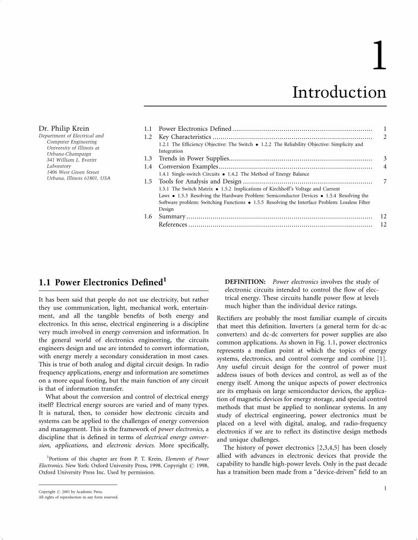
common applications. As shown in Fig. 1.1, power electronics
represents a median point at which the topics of energy
systems, electronics, and control converge and combine [1].
Any useful circuit design for the control of power must
address issues of both devices and control, as well as of the
energy itself. Among the unique aspects of power electronics
are its emphasis on large semiconductor devices, the applica-
tion of magnetic devices for energy storage, and special control
methods that must be applied to nonlinear systems. In any
study of electrical engineering, power electronics must be
placed on a level with digital, analog, and radio-frequency
electronics if we are to reflect its distinctive design methods
and unique challenges.
The history of power electronics [2,3,4,5] has been closely
allied with advances in electronic devices that provide the
capability to handle high-power levels. Only in the past decade
has a transition been made from a ‘‘device-driven’’ field to an
Copyright # 2001 by Academic Press.
All rights of reproduction in any form reserved.
1
1.1 Power Electronics Defined ..................................................................... 1
1.2 Key Characteristics ............................................................................... 21.2.1 The Efficiency Objective: The Switch � 1.2.2 The Reliability Objective: Simplicity and
Integration
1.3 Trends in Power Supplies....................................................................... 3
1.4 Conversion Examples ............................................................................ 41.4.1 Single-switch Circuits � 1.4.2 The Method of Energy Balance
1.5 Tools for Analysis and Design ................................................................ 71.5.1 The Switch Matrix � 1.5.2 Implications of Kirchhoff ’s Voltage and Current
Laws � 1.5.3 Resolving the Hardware Problem: Semiconductor Devices � 1.5.4 Resolving the
Software problem: Switching Functions � 1.5.5 Resolving the Interface Problem: Lossless Filter
Design
1.6 Summary ............................................................................................ 12
References ........................................................................................... 12
1Portions of this chapter are from P. T. Krein, Elements of PowerElectronics. New York: Oxford University Press, 1998. Copyright # 1998,Oxford University Press Inc. Used by permission.
‘‘applications-driven’’ field. This transition has been based on
two factors: advanced semiconductors with suitable power
ratings exist for almost every application of wide interest; and
the general push toward miniaturization is bringing advanced
power electronics into a growing variety of products.
1.2 Key Characteristics
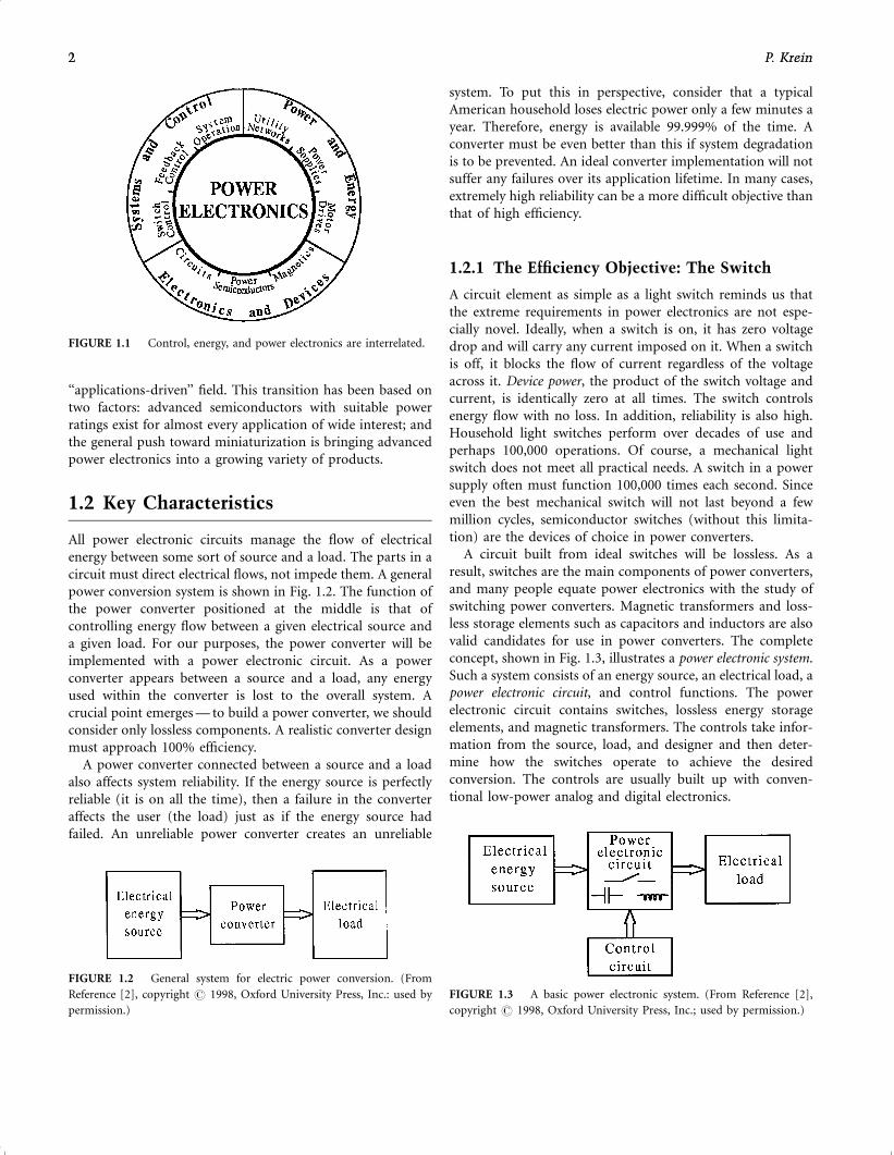
All power electronic circuits manage the flow of electrical
energy between some sort of source and a load. The parts in a
circuit must direct electrical flows, not impede them. A general
power conversion system is shown in Fig. 1.2. The function of
the power converter positioned at the middle is that of
controlling energy flow between a given electrical source and
a given load. For our purposes, the power converter will be
implemented with a power electronic circuit. As a power
converter appears between a source and a load, any energy
used within the converter is lost to the overall system. A
crucial point emerges — to build a power converter, we should
consider only lossless components. A realistic converter design
must approach 100% efficiency.
A power converter connected between a source and a load
also affects system reliability. If the energy source is perfectly
reliable (it is on all the time), then a failure in the converter
affects the user (the load) just as if the energy source had
failed. An unreliable power converter creates an unreliable
system. To put this in perspective, consider that a typical
American household loses electric power only a few minutes a
year. Therefore, energy is available 99.999% of the time. A
converter must be even better than this if system degradation
is to be prevented. An ideal converter implementation will not
suffer any failures over its application lifetime. In many cases,
extremely high reliability can be a more difficult objective than
that of high efficiency.
1.2.1 The Efficiency Objective: The Switch
A circuit element as simple as a light switch reminds us that
the extreme requirements in power electronics are not espe-
cially novel. Ideally, when a switch is on, it has zero voltage
drop and will carry any current imposed on it. When a switch
is off, it blocks the flow of current regardless of the voltage
across it. Device power, the product of the switch voltage and
current, is identically zero at all times. The switch controls
energy flow with no loss. In addition, reliability is also high.
Household light switches perform over decades of use and
perhaps 100,000 operations. Of course, a mechanical light
switch does not meet all practical needs. A switch in a power
supply often must function 100,000 times each second. Since
even the best mechanical switch will not last beyond a few
million cycles, semiconductor switches (without this limita-
tion) are the devices of choice in power converters.
A circuit built from ideal switches will be lossless. As a
result, switches are the main components of power converters,
and many people equate power electronics with the study of
switching power converters. Magnetic transformers and loss-
less storage elements such as capacitors and inductors are also
valid candidates for use in power converters. The complete
concept, shown in Fig. 1.3, illustrates a power electronic system.
Such a system consists of an energy source, an electrical load, a
power electronic circuit, and control functions. The power
electronic circuit contains switches, lossless energy storage
elements, and magnetic transformers. The controls take infor-
mation from the source, load, and designer and then deter-
mine how the switches operate to achieve the desired
conversion. The controls are usually built up with conven-
tional low-power analog and digital electronics.
FIGURE 1.2 General system for electric power conversion. (From
Reference [2], copyright # 1998, Oxford University Press, Inc.: used by
permission.)
FIGURE 1.3 A basic power electronic system. (From Reference [2],
copyright # 1998, Oxford University Press, Inc.; used by permission.)
FIGURE 1.1 Control, energy, and power electronics are interrelated.
2 P. Krein2 P. Krein
Switching devices are selected based on their power handling
rating — the product of their voltage and currents ratings —
rather than on power dissipation ratings. This is in contrast to
other applications of electronics, in which power dissipation
ratings dominate. For instance, a typical stereo receiver
performs a conversion from ac line input to audio output.
Most audio amplifiers do not use the techniques of power
electronics, and the semiconductor devices do not act as
switches. A commercial 100 W amplifier usually is designed
with transistors big enough to dissipate the full 100 W. The
semiconductor devices are used primarily to reconstruct audio
information rather than to manipulate energy flows. When the
devices are used as switches instead, the power levels increase
considerably, as suggested by the following examples.
EXAMPLE 1.1. The 2N2222A is a popular bipolar tran-
sistor with a rated collector-emitter breakdown voltage
of 30 V, a maximum collector current of 0.8 A, and rated
power dissipation of 0.5 W. In a conventional analog
circuit, it usually handles energy within its 0.5 W power
dissipation rating. In principle, this device can manip-
ulate the flow of 0.8 A in a 30 V circuit and so a power
electronics engineer would list its power handling rating
as 24 W. The ability to control up to 24 W, combined
with good switching characteristics, makes this device
common as an auxiliary element in power supplies.
EXAMPLE 1.2. The MTW20N50 is a metal-oxide-semi-
conductor field-effect transistor (MOSFET) with a drain
current rating of 20 A, a maximum drain-source break-
down voltage of 500 V, and rated power dissipation of
250 W. The power handling rating is 10 kW. Several
manufacturers have developed power electronic control-
lers for domestic refrigerators, air conditioners, and even
electric vehicles based on this device and its relatives.
The second part of the definition of power electronics in
Section 1.1 points out that the circuits handle power at levels
much higher than that of the ratings of individual devices.
In the first Example, a 2N2222A might be used to handle
24 W — as compared with its individual rating of 0.5 W. The
MTW20N50 is used to handle up to 10 kW, compared to its
rating of 250 W. These ratios, 48 and 40, respectively, are high,
but not unusual in power electronics contexts. In contrast, the
same ratio in a conventional audio amplifier is close to unity.
1.2.2 The Reliability Objective: Simplicity andIntegration
High-power applications lead to interesting issues. For exam-
ple, in an inverter the semiconductors often manipulate 40
times their rated power or more. A small design error,
unexpected thermal problem, or minor change in layout
could alter this somewhat, perhaps to a factor of 45. This
small change puts large additional stresses on the devices, and
can lead to quick failure. The first issue for reliability in power
electronic circuits is that of managing device voltage, current,
and power dissipation levels to keep them well within rating
limits. This can be challenging when power handling levels are
high.
The second issue for reliability is simplicity. It is well-
established in military electronics that the more parts there
are in a system, the more likely it is to fail. Power electronic
circuits tend to have few parts, especially in the main energy
flow paths. Necessary operations must be carried out through
shrewd use of these parts. Often, this means that sophisticated
control strategies are applied to seemingly simple conversion
circuits.
The third issue for reliability is integration. One way to
avoid the reliability–complexity tradeoff is to integrate multi-
ple components and functions on a single substrate. A micro-
processor, for example, might contain more than a million
gates. As all interconnections and signals flow within a single
chip, the reliability is nearly that of a single part. An important
parallel trend in power electronic devices involves the inte-
grated module [6]. Manufacturers seek ways to package several
switching devices, with their interconnections and protection
components together as a unit. Control circuits for converters
are also integrated as much as possible to keep reliability high.
The package itself becomes a fourth issue for reliability, and
one that is as yet only partly understood. Semiconductor
packages include small bonding wires that can be susceptible
to thermal or vibration damage. The small geometries tend to
enhance electromagnetic interference among the internal
circuit components.
1.3 Trends in Power Supplies
As costs of electronics decline, the power supply becomes a
larger fraction of system cost and design effort. One major
manufacturer estimates that power supply cost will soon reach
50% of the total cost of a typical electronic product such as a
cordless telephone or personal computer. Thus, new technol-
ogy developments in power supplies are critically important.
In the past, bulky linear power supplies were designed with
transformers and rectifiers from the ac line frequency to
provide low-level dc voltages for electronic circuits. Late in
the 1960s, use of dc sources in aerospace applications led to
the development of power electronic dc-dc conversion circuits
for power supplies. In a typical power electronics arrangement
today, an ac source from a wall outlet is rectified without any
transformation; the resulting high dc voltage is converted
through a dc-dc circuit to the 5 V, 12 V, or other level required.
These switched-mode power supplies are rapidly supplanting
linear supplies across the full spectrum of circuit applications.
A personal computer commonly requires three different 5 V
supplies, two þ12 V supplies, a ÿ12 V supply, a 24 V supply,
and perhaps a few more. This does not include supplies for
1 Introduction 3
video display or peripheral devices. Only a switched-mode
supply can support such complex requirements without high
costs. The bulk and weight of linear supplies make them
infeasible for hand-held communication devices, calculators,
notebook computers, and similar equipment. Switched-mode
supplies often take advantage of MOSFET semiconductor
technology. Trends toward high reliability, low cost, and
miniaturization have reached the point at which a 5 V power
supply sold today might last 1,000,000 hr (more than 100 yr),
provide 100 W of output in a package with volume <15 cm3,
and sell for a price of <$0:30 watt. This type of supply brings
an interesting dilemma: the ac line cord to plug it in actually
takes up more space than the power supply itself. Innovative
concepts such as integrating a power supply within a connec-
tion cable will be used in the future.
Device technology for power supplies is being driven by
expanding needs in the automotive and telecommunications
industries as well as in markets for portable equipment. The
automotive industry is making a transition to 42 V systems to
handle increasing electric power needs. Power conversion for
this industry must be cost effective, yet rugged enough to
survive the high vibration and wide temperature range to
which a passenger car is exposed. Global communication is
possible only when sophisticated equipment can be used
almost anywhere. This brings a special challenge, because
electrical supplies are neither reliable nor consistent through-
out much of the world. While in North America voltage
swings in the domestic ac supply are often < �5% around
a nominal value, in many developing nations the swing can be
�25% — when power is available. Power converters for
communications equipment must tolerate these swings, and
must also be able to make use of a wide range of possible
backup sources. Given the enormous size of worldwide
markets for telephones and consumer electronics, there is a
clear need for flexible-source equipment. Designers are
challenged to obtain maximum performance from small
batteries, and to create equipment with minimal energy
requirements.
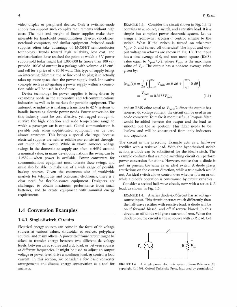
1.4 Conversion Examples
1.4.1 Single-Switch Circuits
Electrical energy sources can come in the form of dc voltage
sources at various values, sinusoidal ac sources, polyphase
sources, and many others. A power electronic circuit might be
asked to transfer energy between two different dc voltage
levels, between an ac source and a dc load, or between sources
at different frequencies. It might be used to adjust an output
voltage or power level, drive a nonlinear load, or control a load
current. In this section, we consider a few basic converter
arrangements and discuss energy conservation as a tool for
analysis.
EXAMPLE 1.3. Consider the circuit shown in Fig. 1.4. It
contains an ac source, a switch, and a resistive load. It is a
simple but complete power electronic system. Let us
assign a (somewhat arbitrary) control scheme to the
switch. What if the switch is turned on whenever
Vac > 0, and turned off otherwise? The input and out-
put voltage waveforms are shown in Fig. 1.5. The input
has a time average of 0, and root mean square (RMS)
value equal to Vpeak=p
2, where Vpeak is the maximum
value of Vac. The output has a nonzero average value
given by:
hvoutðtÞi ¼1
2p
ðp=2
ÿp=2
Vpeak cos y dyþð3p=2
p=2
0 dy� �
¼Vpeak
p¼ 0:3183Vpeak ð1:1Þ
and an RMS value equal to Vpeak=2. Since the output has
nonzero dc voltage content, the circuit can be used as an
ac-dc converter. To make it more useful, a lowpass filter
would be added between the output and the load to
smooth out the ac portion. This filter needs to be
lossless, and will be constructed from only inductors
and capacitors.
The circuit in the preceding Example acts as a half-wave
rectifier with a resistive load. With the hypothesized switch
action, a diode can be substituted for the ideal switch. The
example confirms that a simple switching circuit can perform
power conversion functions. However, notice that a diode is
not, in general, the same as an ideal switch. A diode places
restrictions on the current direction, while a true switch would
not. An ideal switch allows control over whether it is on or off,
while a diode’s operation is constrained by circuit variables.
Consider a second half-wave circuit, now with a series L-R
load, as shown in Fig. 1.6.
EXAMPLE 1.4. A series diode-L-R circuit has ac voltage-
source input. This circuit operates much differently than
the half-wave rectifier with resistive load. A diode will be
on if forward biased, and off if reverse biased. In this
circuit, an off diode will give a current of zero. When the
diode is on, the circuit is the ac source with L-R load. Let
FIGURE 1.4 A simple power electronic system. (From Reference [2],
copyright # 1998, Oxford University Press, Inc.; used by permission.)
4 P. Krein4 P. Krein
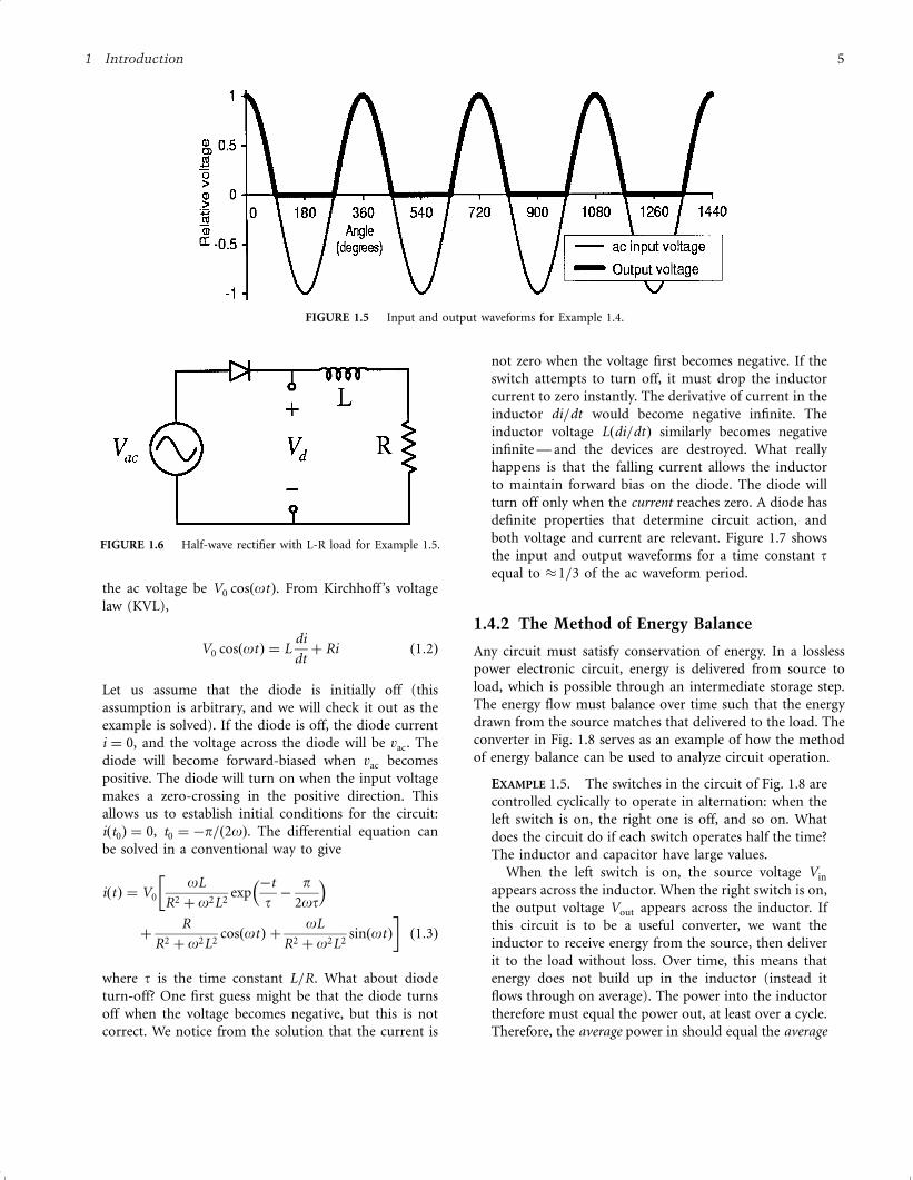
the ac voltage be V0 cosðotÞ. From Kirchhoff ’s voltage
law (KVL),
V0 cosðotÞ ¼ Ldi
dtþ Ri ð1:2Þ
Let us assume that the diode is initially off (this
assumption is arbitrary, and we will check it out as the
example is solved). If the diode is off, the diode current
i ¼ 0, and the voltage across the diode will be vac. The
diode will become forward-biased when vac becomes
positive. The diode will turn on when the input voltage
makes a zero-crossing in the positive direction. This
allows us to establish initial conditions for the circuit:
iðt0Þ ¼ 0, t0 ¼ ÿp=ð2oÞ. The differential equation can
be solved in a conventional way to give
iðtÞ ¼ V0
oL
R2 þ o2L2expÿt
tÿ
p2ot
� ��þ
R
R2 þ o2L2cosðotÞ þ
oL
R2 þ o2L2sinðotÞ
�ð1:3Þ
where t is the time constant L=R. What about diode
turn-off? One first guess might be that the diode turns
off when the voltage becomes negative, but this is not
correct. We notice from the solution that the current is
not zero when the voltage first becomes negative. If the
switch attempts to turn off, it must drop the inductor
current to zero instantly. The derivative of current in the
inductor di=dt would become negative infinite. The
inductor voltage Lðdi=dtÞ similarly becomes negative
infinite — and the devices are destroyed. What really
happens is that the falling current allows the inductor
to maintain forward bias on the diode. The diode will
turn off only when the current reaches zero. A diode has
definite properties that determine circuit action, and
both voltage and current are relevant. Figure 1.7 shows
the input and output waveforms for a time constant tequal to �1=3 of the ac waveform period.
1.4.2 The Method of Energy Balance
Any circuit must satisfy conservation of energy. In a lossless
power electronic circuit, energy is delivered from source to
load, which is possible through an intermediate storage step.
The energy flow must balance over time such that the energy
drawn from the source matches that delivered to the load. The
converter in Fig. 1.8 serves as an example of how the method
of energy balance can be used to analyze circuit operation.
EXAMPLE 1.5. The switches in the circuit of Fig. 1.8 are
controlled cyclically to operate in alternation: when the
left switch is on, the right one is off, and so on. What
does the circuit do if each switch operates half the time?
The inductor and capacitor have large values.
When the left switch is on, the source voltage Vin
appears across the inductor. When the right switch is on,
the output voltage Vout appears across the inductor. If
this circuit is to be a useful converter, we want the
inductor to receive energy from the source, then deliver
it to the load without loss. Over time, this means that
energy does not build up in the inductor (instead it
flows through on average). The power into the inductor
therefore must equal the power out, at least over a cycle.
Therefore, the average power in should equal the average
FIGURE 1.5 Input and output waveforms for Example 1.4.
FIGURE 1.6 Half-wave rectifier with L-R load for Example 1.5.
1 Introduction 5
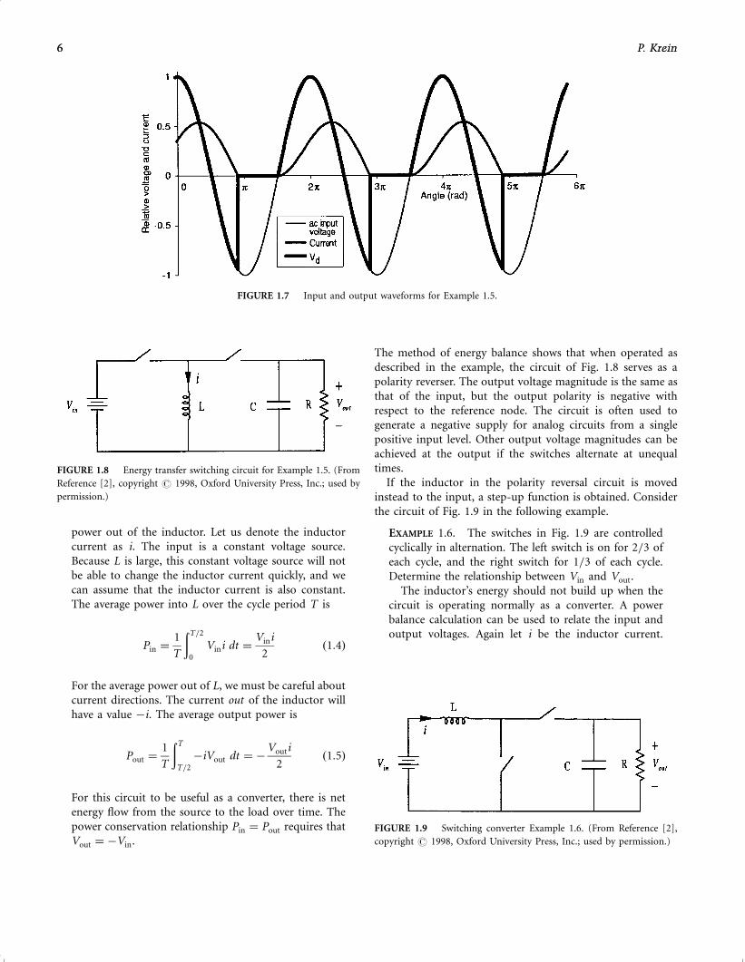
power out of the inductor. Let us denote the inductor
current as i. The input is a constant voltage source.
Because L is large, this constant voltage source will not
be able to change the inductor current quickly, and we
can assume that the inductor current is also constant.
The average power into L over the cycle period T is
Pin ¼1
T
ðT=2
0
Vini dt ¼Vini
2ð1:4Þ
For the average power out of L, we must be careful about
current directions. The current out of the inductor will
have a value ÿi. The average output power is
Pout ¼1
T
ðT
T=2
ÿiVout dt ¼ ÿVouti
2ð1:5Þ
For this circuit to be useful as a converter, there is net
energy flow from the source to the load over time. The
power conservation relationship Pin ¼ Pout requires that
Vout ¼ ÿVin.
The method of energy balance shows that when operated as
described in the example, the circuit of Fig. 1.8 serves as a
polarity reverser. The output voltage magnitude is the same as
that of the input, but the output polarity is negative with
respect to the reference node. The circuit is often used to
generate a negative supply for analog circuits from a single
positive input level. Other output voltage magnitudes can be
achieved at the output if the switches alternate at unequal
times.
If the inductor in the polarity reversal circuit is moved
instead to the input, a step-up function is obtained. Consider
the circuit of Fig. 1.9 in the following example.
EXAMPLE 1.6. The switches in Fig. 1.9 are controlled
cyclically in alternation. The left switch is on for 2=3 of
each cycle, and the right switch for 1=3 of each cycle.
Determine the relationship between Vin and Vout.
The inductor’s energy should not build up when the
circuit is operating normally as a converter. A power
balance calculation can be used to relate the input and
output voltages. Again let i be the inductor current.
FIGURE 1.8 Energy transfer switching circuit for Example 1.5. (From
Reference [2], copyright # 1998, Oxford University Press, Inc.; used by
permission.)
FIGURE 1.9 Switching converter Example 1.6. (From Reference [2],
copyright # 1998, Oxford University Press, Inc.; used by permission.)
FIGURE 1.7 Input and output waveforms for Example 1.5.
6 P. Krein6 P. Krein
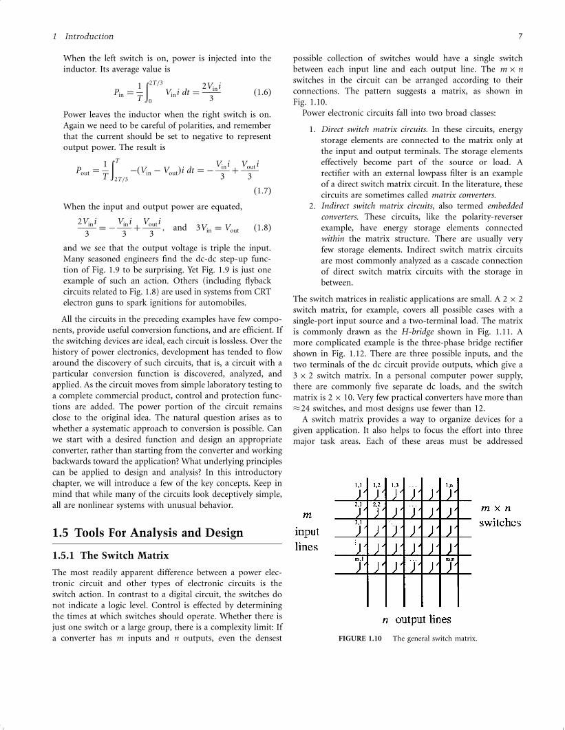
When the left switch is on, power is injected into the
inductor. Its average value is
Pin ¼1
T
ð2T=3
0
Vini dt ¼2Vini
3ð1:6Þ
Power leaves the inductor when the right switch is on.
Again we need to be careful of polarities, and remember
that the current should be set to negative to represent
output power. The result is
Pout ¼1
T
ðT
2T=3
ÿðVin ÿ VoutÞi dt ¼ ÿVini
3þ
Vouti
3
ð1:7Þ
When the input and output power are equated,
2Vini
3¼ ÿ
Vini
3þ
Vouti
3; and 3Vin ¼ Vout ð1:8Þ
and we see that the output voltage is triple the input.
Many seasoned engineers find the dc-dc step-up func-
tion of Fig. 1.9 to be surprising. Yet Fig. 1.9 is just one
example of such an action. Others (including flyback
circuits related to Fig. 1.8) are used in systems from CRT
electron guns to spark ignitions for automobiles.
All the circuits in the preceding examples have few compo-
nents, provide useful conversion functions, and are efficient. If
the switching devices are ideal, each circuit is lossless. Over the
history of power electronics, development has tended to flow
around the discovery of such circuits, that is, a circuit with a
particular conversion function is discovered, analyzed, and
applied. As the circuit moves from simple laboratory testing to
a complete commercial product, control and protection func-
tions are added. The power portion of the circuit remains
close to the original idea. The natural question arises as to
whether a systematic approach to conversion is possible. Can
we start with a desired function and design an appropriate
converter, rather than starting from the converter and working
backwards toward the application? What underlying principles
can be applied to design and analysis? In this introductory
chapter, we will introduce a few of the key concepts. Keep in
mind that while many of the circuits look deceptively simple,
all are nonlinear systems with unusual behavior.
1.5 Tools For Analysis and Design
1.5.1 The Switch Matrix
The most readily apparent difference between a power elec-
tronic circuit and other types of electronic circuits is the
switch action. In contrast to a digital circuit, the switches do
not indicate a logic level. Control is effected by determining
the times at which switches should operate. Whether there is
just one switch or a large group, there is a complexity limit: If
a converter has m inputs and n outputs, even the densest
possible collection of switches would have a single switch
between each input line and each output line. The m� n
switches in the circuit can be arranged according to their
connections. The pattern suggests a matrix, as shown in
Fig. 1.10.
Power electronic circuits fall into two broad classes:
1. Direct switch matrix circuits. In these circuits, energy
storage elements are connected to the matrix only at
the input and output terminals. The storage elements
effectively become part of the source or load. A
rectifier with an external lowpass filter is an example
of a direct switch matrix circuit. In the literature, these
circuits are sometimes called matrix converters.
2. Indirect switch matrix circuits, also termed embedded
converters. These circuits, like the polarity-reverser
example, have energy storage elements connected
within the matrix structure. There are usually very
few storage elements. Indirect switch matrix circuits
are most commonly analyzed as a cascade connection
of direct switch matrix circuits with the storage in
between.
The switch matrices in realistic applications are small. A 2� 2
switch matrix, for example, covers all possible cases with a
single-port input source and a two-terminal load. The matrix
is commonly drawn as the H-bridge shown in Fig. 1.11. A
more complicated example is the three-phase bridge rectifier
shown in Fig. 1.12. There are three possible inputs, and the
two terminals of the dc circuit provide outputs, which give a
3� 2 switch matrix. In a personal computer power supply,
there are commonly five separate dc loads, and the switch
matrix is 2� 10. Very few practical converters have more than
�24 switches, and most designs use fewer than 12.
A switch matrix provides a way to organize devices for a
given application. It also helps to focus the effort into three
major task areas. Each of these areas must be addressed
FIGURE 1.10 The general switch matrix.
1 Introduction 7
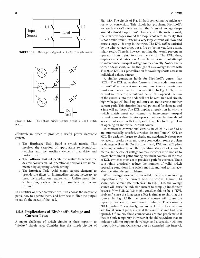
effectively in order to produce a useful power electronic
system.
� The Hardware Task!Build a switch matrix. This
involves the selection of appropriate semiconductor
switches and the auxiliary elements that drive and
protect them.
� The Software Task!Operate the matrix to achieve the
desired conversion. All operational decisions are imple-
mented by adjusting switch timing.
� The Interface Task!Add energy storage elements to
provide the filters or intermediate storage necessary to
meet the application requirements. Unlike most filter
applications, lossless filters with simple structures are
required.
In a rectifier or other converter, we must choose the electronic
parts, how to operate them, and how best to filter the output
to satisfy the needs of the load.
1.5.2 Implications of Kirchhoff’s Voltage andCurrent Laws
A major challenge of switch circuits is their capacity to
‘‘violate’’ circuit laws. Consider first the simple circuits of
Fig. 1.13. The circuit of Fig. 1.13a is something we might try
for ac-dc conversion. This circuit has problems. Kirchhoff ’s
voltage law (KVL) tells us that the ‘‘sum of voltage drops
around a closed loop is zero.’’ However, with the switch closed,
the sum of voltages around the loop is not zero. In reality, this
is not a valid result. Instead, a very large current will flow and
cause a large I � R drop in the wires. The KVL will be satisfied
by the wire voltage drop, but a fire or, better yet, fuse action,
might result. There is, however, nothing that would prevent an
operator from trying to close the switch. The KVL, then,
implies a crucial restriction: A switch matrix must not attempt
to interconnect unequal voltage sources directly. Notice that a
wire, or dead short, can be thought of as a voltage source with
V ¼ 0, so KVL is a generalization for avoiding shorts across an
individual voltage source.
A similar constraint holds for Kirchhoff ’s current law
(KCL). The KCL states that ‘‘currents into a node must sum
to zero.’’ When current sources are present in a converter, we
must avoid any attempts to violate KCL. In Fig. 1.13b, if the
current sources are different and the switch is opened, the sum
of the currents into the node will not be zero. In a real circuit,
high voltages will build up and cause an arc to create another
current path. This situation has real potential for damage, and
a fuse will not help. The KCL implies a restriction in which a
switch matrix must not attempt to interconnect unequal
current sources directly. An open circuit can be thought of
as a current source with I ¼ 0, so KCL applies to the problem
of opening an individual current source.
In contrast to conventional circuits, in which KVL and KCL
are automatically satisfied, switches do not ‘‘know’’ KVL or
KCL. If a designer forgets to check, and accidentally shorts two
voltages or breaks a current source connection, some problem
or damage will result. On the other hand, KVL and KCL place
necessary constraints on the operating strategy of a switch
matrix. In the case of voltage sources, switches must not act to
create short-circuit paths among dissimilar sources. In the case
of KCL, switches must act to provide a path for currents. These
constraints drastically reduce the number of valid switch
operating conditions in a switch matrix, and lead to manage-
able operating design problems.
When energy storage is included, there are interesting
implications for the current law restrictions. Figure 1.14
shows two ‘‘circuit law problems.’’ In Fig. 1.14a, the voltage
source will cause the inductor current to ramp up indefinitely
because V ¼ L di=dt . We might consider this to be a ‘‘KVL
problem,’’ since the long-term effect is similar to shorting the
source. In Fig. 1.14b, the current source will cause the
capacitor voltage to ramp toward infinity. This causes a
‘‘KCL problem’’; eventually, an arc will form to create an
additional current path, just as if the current source had been
opened. Of course, these connections are not problematic if
they are only temporary. However, it should be evident that an
inductor will not support dc voltage, and a capacitor will not
support dc current. On average over an extended time interval,
Load
1,2
2,2
InputSource
1,1
2,1
FIGURE 1.11 H-bridge configuration of a 2� 2 switch matrix..
b
c
Dcload
a
v
v
v
FIGURE 1.12 Three-phase bridge rectifier circuit, a 3� 2 switch
matrix.
8 P. Krein8 P. Krein
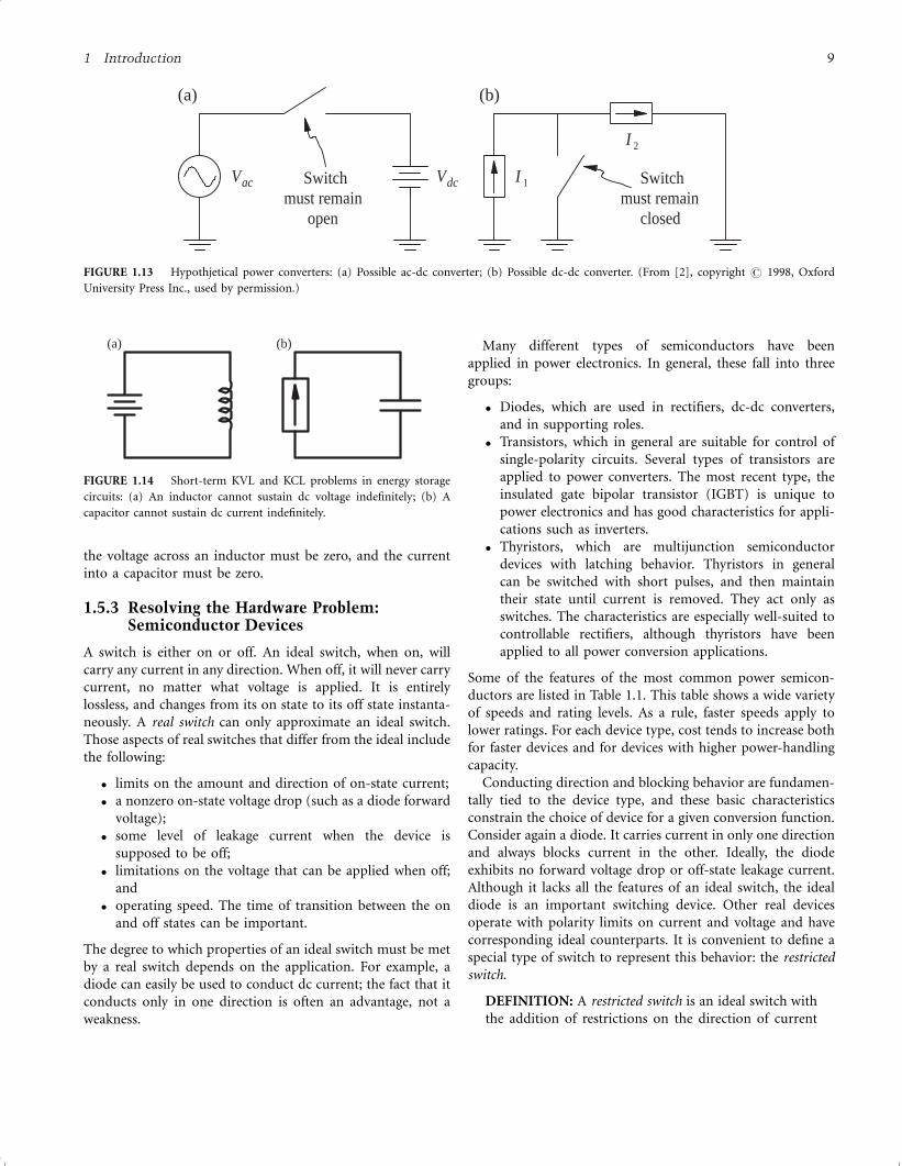
the voltage across an inductor must be zero, and the current
into a capacitor must be zero.
1.5.3 Resolving the Hardware Problem:Semiconductor Devices
A switch is either on or off. An ideal switch, when on, will
carry any current in any direction. When off, it will never carry
current, no matter what voltage is applied. It is entirely
lossless, and changes from its on state to its off state instanta-
neously. A real switch can only approximate an ideal switch.
Those aspects of real switches that differ from the ideal include
the following:
� limits on the amount and direction of on-state current;
� a nonzero on-state voltage drop (such as a diode forward
voltage);
� some level of leakage current when the device is
supposed to be off;
� limitations on the voltage that can be applied when off;
and
� operating speed. The time of transition between the on
and off states can be important.
The degree to which properties of an ideal switch must be met
by a real switch depends on the application. For example, a
diode can easily be used to conduct dc current; the fact that it
conducts only in one direction is often an advantage, not a
weakness.
Many different types of semiconductors have been
applied in power electronics. In general, these fall into three
groups:
� Diodes, which are used in rectifiers, dc-dc converters,
and in supporting roles.
� Transistors, which in general are suitable for control of
single-polarity circuits. Several types of transistors are
applied to power converters. The most recent type, the
insulated gate bipolar transistor (IGBT) is unique to
power electronics and has good characteristics for appli-
cations such as inverters.
� Thyristors, which are multijunction semiconductor
devices with latching behavior. Thyristors in general
can be switched with short pulses, and then maintain
their state until current is removed. They act only as
switches. The characteristics are especially well-suited to
controllable rectifiers, although thyristors have been
applied to all power conversion applications.
Some of the features of the most common power semicon-
ductors are listed in Table 1.1. This table shows a wide variety
of speeds and rating levels. As a rule, faster speeds apply to
lower ratings. For each device type, cost tends to increase both
for faster devices and for devices with higher power-handling
capacity.
Conducting direction and blocking behavior are fundamen-
tally tied to the device type, and these basic characteristics
constrain the choice of device for a given conversion function.
Consider again a diode. It carries current in only one direction
and always blocks current in the other. Ideally, the diode
exhibits no forward voltage drop or off-state leakage current.
Although it lacks all the features of an ideal switch, the ideal
diode is an important switching device. Other real devices
operate with polarity limits on current and voltage and have
corresponding ideal counterparts. It is convenient to define a
special type of switch to represent this behavior: the restricted
switch.
DEFINITION: A restricted switch is an ideal switch with
the addition of restrictions on the direction of current
(a) (b)
FIGURE 1.14 Short-term KVL and KCL problems in energy storage
circuits: (a) An inductor cannot sustain dc voltage indefinitely; (b) A
capacitor cannot sustain dc current indefinitely.
dcacV VSwitchmust remain
open
Switchmust remain
closed
I
I
1
2
(b)(a)
FIGURE 1.13 Hypothjetical power converters: (a) Possible ac-dc converter; (b) Possible dc-dc converter. (From [2], copyright # 1998, Oxford
University Press Inc., used by permission.)
1 Introduction 9
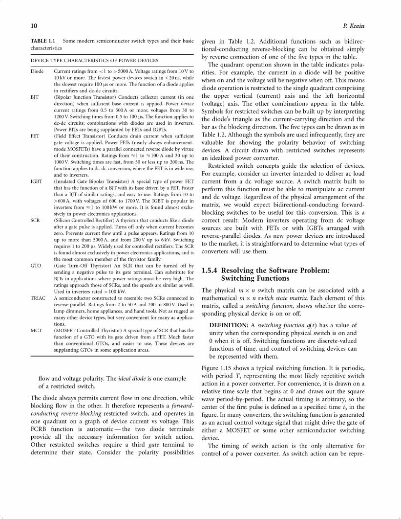
flow and voltage polarity. The ideal diode is one example
of a restricted switch.
The diode always permits current flow in one direction, while
blocking flow in the other. It therefore represents a forward-
conducting reverse-blocking restricted switch, and operates in
one quadrant on a graph of device current vs voltage. This
FCRB function is automatic — the two diode terminals
provide all the necessary information for switch action.
Other restricted switches require a third gate terminal to
determine their state. Consider the polarity possibilities
given in Table 1.2. Additional functions such as bidirec-
tional-conducting reverse-blocking can be obtained simply
by reverse connection of one of the five types in the table.
The quadrant operation shown in the table indicates pola-
rities. For example, the current in a diode will be positive
when on and the voltage will be negative when off. This means
diode operation is restricted to the single quadrant comprising
the upper vertical (current) axis and the left horizontal
(voltage) axis. The other combinations appear in the table.
Symbols for restricted switches can be built up by interpreting
the diode’s triangle as the current-carrying direction and the
bar as the blocking direction. The five types can be drawn as in
Table 1.2. Although the symbols are used infrequently, they are
valuable for showing the polarity behavior of switching
devices. A circuit drawn with restricted switches represents
an idealized power converter.
Restricted switch concepts guide the selection of devices.
For example, consider an inverter intended to deliver ac load
current from a dc voltage source. A switch matrix built to
perform this function must be able to manipulate ac current
and dc voltage. Regardless of the physical arrangement of the
matrix, we would expect bidirectional-conducting forward-
blocking switches to be useful for this conversion. This is a
correct result: Modern inverters operating from dc voltage
sources are built with FETs or with IGBTs arranged with
reverse-parallel diodes. As new power devices are introduced
to the market, it is straightforward to determine what types of
converters will use them.
1.5.4 Resolving the Software Problem:Switching Functions
The physical m� n switch matrix can be associated with a
mathematical m� n switch state matrix. Each element of this
matrix, called a switching function, shows whether the corre-
sponding physical device is on or off.
DEFINITION: A switching function qðtÞ has a value of
unity when the corresponding physical switch is on and
0 when it is off. Switching functions are discrete-valued
functions of time, and control of switching devices can
be represented with them.
Figure 1.15 shows a typical switching function. It is periodic,
with period T , representing the most likely repetitive switch
action in a power converter. For convenience, it is drawn on a
relative time scale that begins at 0 and draws out the square
wave period-by-period. The actual timing is arbitrary, so the
center of the first pulse is defined as a specified time t0 in the
figure. In many converters, the switching function is generated
as an actual control voltage signal that might drive the gate of
either a MOSFET or some other semiconductor switching
device.
The timing of switch action is the only alternative for
control of a power converter. As switch action can be repre-
TABLE 1.1 Some modern semiconductor switch types and their basic
characteristics
DEVICE TYPE CHARACTERISTICS OF POWER DEVICES
Diode Current ratings from <1 to >5000 A. Voltage ratings from 10 V to
10 kV or more. The fastest power devices switch in < 20 ns, while
the slowest require 100 ms or more. The function of a diode applies
in rectifiers and dc-dc circuits.
BJT (Bipolar Junction Transistor) Conducts collector current (in one
direction) when sufficient base current is applied. Power device
current ratings from 0.5 to 500 A or more; voltages from 30 to
1200 V. Switching times from 0.5 to 100 ms. The function applies to
dc-dc circuits; combinations with diodes are used in inverters.
Power BJTs are being supplanted by FETs and IGBTs.
FET (Field Effect Transistor) Conducts drain current when sufficient
gate voltage is applied. Power FETs (nearly always enhancement-
mode MOSFETs) have a parallel connected reverse diode by virtue
of their construction. Ratings from �1 to �100 A and 30 up to
1000 V. Switching times are fast, from 50 or less up to 200 ns. The
function applies to dc-dc conversion, where the FET is in wide use,
and to inverters.
IGBT (Insulated Gate Bipolar Transistor) A special type of power FET
that has the function of a BJT with its base driven by a FET. Faster
than a BJT of similar ratings, and easy to use. Ratings from 10 to
> 600 A, with voltages of 600 to 1700 V. The IGBT is popular in
inverters from �1 to 100 kW or more. It is found almost exclu-
sively in power electronics applications.
SCR (Silicon Controlled Rectifier) A thyristor that conducts like a diode
after a gate pulse is applied. Turns off only when current becomes
zero. Prevents current flow until a pulse appears. Ratings from 10
up to more than 5000 A, and from 200 V up to 6 kV. Switching
requires 1 to 200 ms. Widely used for controlled rectifiers. The SCR
is found almost exclusively in power electronics applications, and is
the most common member of the thyristor family.
GTO (Gate Turn-Off Thyristor) An SCR that can be turned off by
sending a negative pulse to its gate terminal. Can substitute for
BJTs in applications where power ratings must be very high. The
ratings approach those of SCRs, and the speeds are similar as well.
Used in inverters rated >100 kW.
TRIAC A semiconductor constructed to resemble two SCRs connected in
reverse parallel. Ratings from 2 to 50 A and 200 to 800 V. Used in
lamp dimmers, home appliances, and hand tools. Not as rugged as
many other device types, but very convenient for many ac applica-
tions.
MCT (MOSFET Controlled Thyristor) A special type of SCR that has the
function of a GTO with its gate driven from a FET. Much faster
than conventional GTOs, and easier to use. These devices are
supplanting GTOs in some application areas.
10 P. Krein10 P. Krein
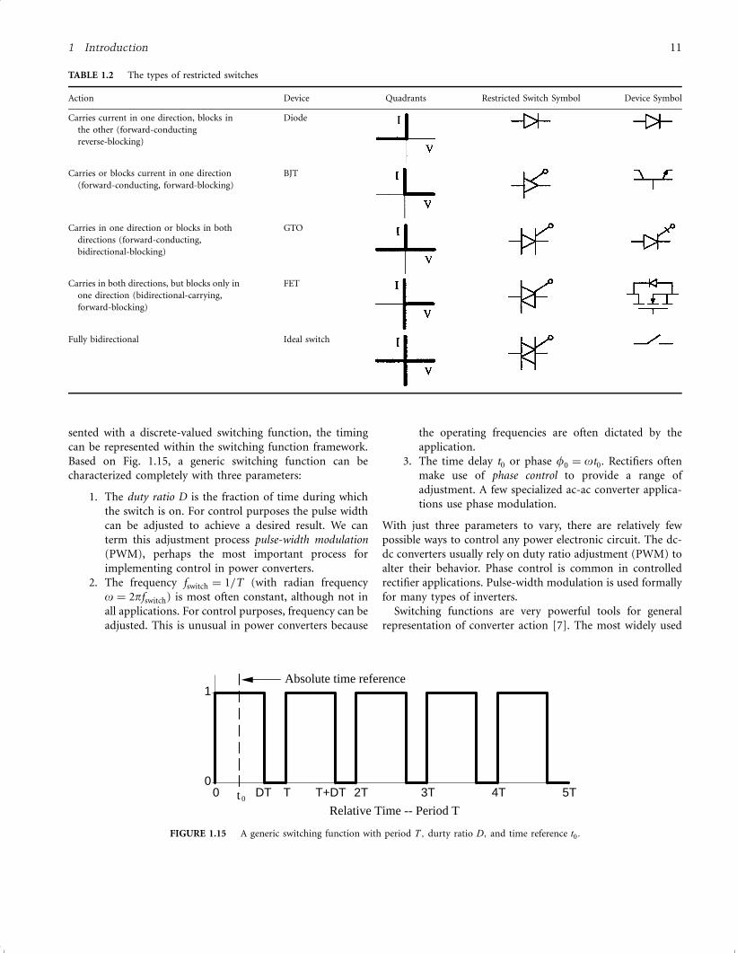
sented with a discrete-valued switching function, the timing
can be represented within the switching function framework.
Based on Fig. 1.15, a generic switching function can be
characterized completely with three parameters:
1. The duty ratio D is the fraction of time during which
the switch is on. For control purposes the pulse width
can be adjusted to achieve a desired result. We can
term this adjustment process pulse-width modulation
(PWM), perhaps the most important process for
implementing control in power converters.
2. The frequency fswitch ¼ 1=T (with radian frequency
o ¼ 2pfswitch) is most often constant, although not in
all applications. For control purposes, frequency can be
adjusted. This is unusual in power converters because
the operating frequencies are often dictated by the
application.
3. The time delay t0 or phase f0 ¼ ot0. Rectifiers often
make use of phase control to provide a range of
adjustment. A few specialized ac-ac converter applica-
tions use phase modulation.
With just three parameters to vary, there are relatively few
possible ways to control any power electronic circuit. The dc-
dc converters usually rely on duty ratio adjustment (PWM) to
alter their behavior. Phase control is common in controlled
rectifier applications. Pulse-width modulation is used formally
for many types of inverters.
Switching functions are very powerful tools for general
representation of converter action [7]. The most widely used
TABLE 1.2 The types of restricted switches
Action Device Quadrants Restricted Switch Symbol Device Symbol
Carries current in one direction, blocks in
the other (forward-conducting
reverse-blocking)
Diode
Carries or blocks current in one direction
(forward-conducting, forward-blocking)
BJT
Carries in one direction or blocks in both
directions (forward-conducting,
bidirectional-blocking)
GTO
Carries in both directions, but blocks only in
one direction (bidirectional-carrying,
forward-blocking)
FET
Fully bidirectional Ideal switch
0
1
0 DT T T+DT 2T 3T 4T 5T
Relative Time -- Period Tt
Absolute time reference
0
FIGURE 1.15 A generic switching function with period T ; durty ratio D; and time reference t0:
1 Introduction 11
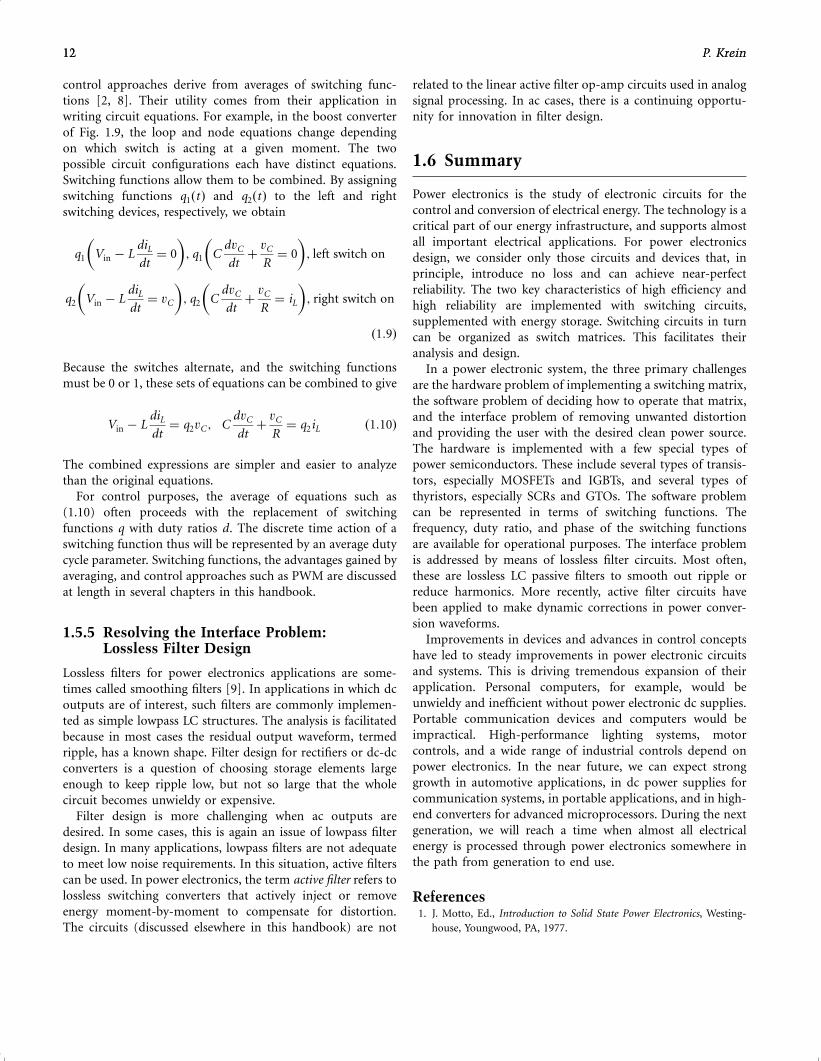
control approaches derive from averages of switching func-
tions [2, 8]. Their utility comes from their application in
writing circuit equations. For example, in the boost converter
of Fig. 1.9, the loop and node equations change depending
on which switch is acting at a given moment. The two
possible circuit configurations each have distinct equations.
Switching functions allow them to be combined. By assigning
switching functions q1ðtÞ and q2ðtÞ to the left and right
switching devices, respectively, we obtain
q1 Vin ÿ LdiL
dt¼ 0
� �; q1 C
dvC
dtþ
vC
R¼ 0
� �; left switch on
q2 Vin ÿ LdiL
dt¼ vC
� �; q2 C
dvC
dtþ
vC
R¼ iL
� �; right switch on
ð1:9Þ
Because the switches alternate, and the switching functions
must be 0 or 1, these sets of equations can be combined to give
Vin ÿ LdiL
dt¼ q2vC; C
dvC
dtþ
vC
R¼ q2iL ð1:10Þ
The combined expressions are simpler and easier to analyze
than the original equations.
For control purposes, the average of equations such as
(1.10) often proceeds with the replacement of switching
functions q with duty ratios d. The discrete time action of a
switching function thus will be represented by an average duty
cycle parameter. Switching functions, the advantages gained by
averaging, and control approaches such as PWM are discussed
at length in several chapters in this handbook.
1.5.5 Resolving the Interface Problem:Lossless Filter Design
Lossless filters for power electronics applications are some-
times called smoothing filters [9]. In applications in which dc
outputs are of interest, such filters are commonly implemen-
ted as simple lowpass LC structures. The analysis is facilitated
because in most cases the residual output waveform, termed
ripple, has a known shape. Filter design for rectifiers or dc-dc
converters is a question of choosing storage elements large
enough to keep ripple low, but not so large that the whole
circuit becomes unwieldy or expensive.
Filter design is more challenging when ac outputs are
desired. In some cases, this is again an issue of lowpass filter
design. In many applications, lowpass filters are not adequate
to meet low noise requirements. In this situation, active filters
can be used. In power electronics, the term active filter refers to
lossless switching converters that actively inject or remove
energy moment-by-moment to compensate for distortion.
The circuits (discussed elsewhere in this handbook) are not
related to the linear active filter op-amp circuits used in analog
signal processing. In ac cases, there is a continuing opportu-
nity for innovation in filter design.
1.6 Summary
Power electronics is the study of electronic circuits for the
control and conversion of electrical energy. The technology is a
critical part of our energy infrastructure, and supports almost
all important electrical applications. For power electronics
design, we consider only those circuits and devices that, in
principle, introduce no loss and can achieve near-perfect
reliability. The two key characteristics of high efficiency and
high reliability are implemented with switching circuits,
supplemented with energy storage. Switching circuits in turn
can be organized as switch matrices. This facilitates their
analysis and design.
In a power electronic system, the three primary challenges
are the hardware problem of implementing a switching matrix,
the software problem of deciding how to operate that matrix,
and the interface problem of removing unwanted distortion
and providing the user with the desired clean power source.
The hardware is implemented with a few special types of
power semiconductors. These include several types of transis-
tors, especially MOSFETs and IGBTs, and several types of
thyristors, especially SCRs and GTOs. The software problem
can be represented in terms of switching functions. The
frequency, duty ratio, and phase of the switching functions
are available for operational purposes. The interface problem
is addressed by means of lossless filter circuits. Most often,
these are lossless LC passive filters to smooth out ripple or
reduce harmonics. More recently, active filter circuits have
been applied to make dynamic corrections in power conver-
sion waveforms.
Improvements in devices and advances in control concepts
have led to steady improvements in power electronic circuits
and systems. This is driving tremendous expansion of their
application. Personal computers, for example, would be
unwieldy and inefficient without power electronic dc supplies.
Portable communication devices and computers would be
impractical. High-performance lighting systems, motor
controls, and a wide range of industrial controls depend on
power electronics. In the near future, we can expect strong
growth in automotive applications, in dc power supplies for
communication systems, in portable applications, and in high-
end converters for advanced microprocessors. During the next
generation, we will reach a time when almost all electrical
energy is processed through power electronics somewhere in
the path from generation to end use.
References1. J. Motto, Ed., Introduction to Solid State Power Electronics, Westing-
house, Youngwood, PA, 1977.
12 P. Krein12 P. Krein

2. P. T. Krein, Elements of Power Electronics, Oxford University Press,
New York, 1998.
3. T. M. Jahns and E. L. Owen, ‘‘Ac adjustable-speed drives at the
millenium: how did we get here?’’ in Proc. IEEE Applied Power
Electronics Conf., 2000, pp. 18–26.
4. C. C. Herskind and W. McMurray, ‘‘History of the Static Power
Converter Committee,’’ IEEE Trans. Industry Applications IA-20:4,
1069–1072 (1984).
5. E. L. Owen, ‘‘Origins of the inverter,’’ IEEE Industry Applications Mag.
2: 64 (1996).
6. J. D. Van Wyk and F. C. Lee, ‘‘Power electronics technology at the
dawn of the new millenium — status and future,’’ in Rec., IEEE Power
Electronics Specialists Conf., 1999, pp. 3–12.
7. P. Wood, Switching Power Converters, Van Nostrand Reinhold, New
York 1981.
8. R. Erickson, Fundamentals of Power Electronics, Chapman and Hall,
New York, 1997.
9. P. T. Krein and D. C. Hamill, ‘‘Smoothing circuits,’’ in Wiley Encyclo-
pedia of Electrical and Electronics Engineering, J. Webster, ed., John
Wiley, New York, 1999.
1 Introduction 13
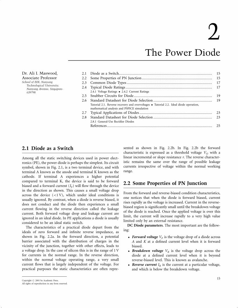
2The Power Diode
Dr. Ali I. Maswood,Associate ProfessorSchool of EEE, Nanyang
Technological University,
Nanyang Avenue, Singapore-
639798
2.1 Diode as a Switch
Among all the static switching devices used in power elect-
ronics (PE), the power diode is perhaps the simplest. Its circuit
symbol, shown in Fig. 2.1, is a two terminal device, and with
terminal A known as the anode and terminal K known as the
cathode. If terminal A experiences a higher potential
compared to terminal K, the device is said to be forward
biased and a forward current (IF) will flow through the device
in the direction as shown. This causes a small voltage drop
across the device (<1 V), which under ideal conditions is
usually ignored. By contrast, when a diode is reverse biased, it
does not conduct and the diode then experiences a small
current flowing in the reverse direction called the leakage
current. Both forward voltage drop and leakage current are
ignored in an ideal diode. In PE applications a diode is usually
considered to be an ideal static switch.
The characteristics of a practical diode depart from the
ideals of zero forward and infinite reverse impedance, as
shown in Fig. 2.2a. In the forward direction, a potential
barrier associated with the distribution of charges in the
vicinity of the junction, together with other effects, leads to
a voltage drop. In the case of silicon this is in the range of 1 V
for currents in the normal range. In the reverse direction,
within the normal voltage operating range, a very small
current flows that is largely independent of the voltage. For
practical purposes the static characteristics are often repre-
sented as shown in Fig. 2.2b. In Fig. 2.2b the forward
characteristic is expressed as a threshold voltage VO with a
linear incremental or slope resistance r. The reverse character-
istic remains the same over the range of possible leakage
currents irrespective of voltage within the normal working
range.
2.2 Some Properties of PN Junction
From the forward and reverse-biased condition characteristics,
one notices that when the diode is forward biased, current
rises rapidly as the voltage is increased. Current in the reverse-
biased region is significantly small until the breakdown voltage
of the diode is reached. Once the applied voltage is over this
limit, the current will increase rapidly to a very high value
limited only by an external resistance.
DC Diode parameters. The most important are the follow-
ing:
� Forward voltage VF is the voltage drop of a diode across
A and K at a defined current level when it is forward
biased.
� Breakdown voltage VB is the voltage drop across the
diode at a defined current level when it is beyond
reverse-biased level. This is known as avalanche.
� Reverse current IR is the current at a particular voltage,
and which is below the breakdown voltage.
Copyright # 2001 by Academic Press.
All rights of reproduction in any form reserved.
15
2.1 Diode as a Switch................................................................................. 15
2.2 Some Properties of PN Junction ............................................................. 15
2.3 Common Diode Types .......................................................................... 17
2.4 Typical Diode Ratings ........................................................................... 172.4.1 Voltage Ratings � 2.4.2 Current Ratings
2.5 Snubber Circuits for Diode.................................................................... 19
2.6 Standard Datasheet for Diode Selection ................................................... 19Tutorial 2.1. Reverse recovery and overvoltages � Tutorial 2.2. Ideal diode operation,
mathematical analysis and PSPICE simulation
2.7 Typical Applications of Diodes ............................................................... 23
2.8 Standard Datasheet for Diode Selection ................................................... 232.8.1 General-Use Rectifier Diodes
References ........................................................................................... 25
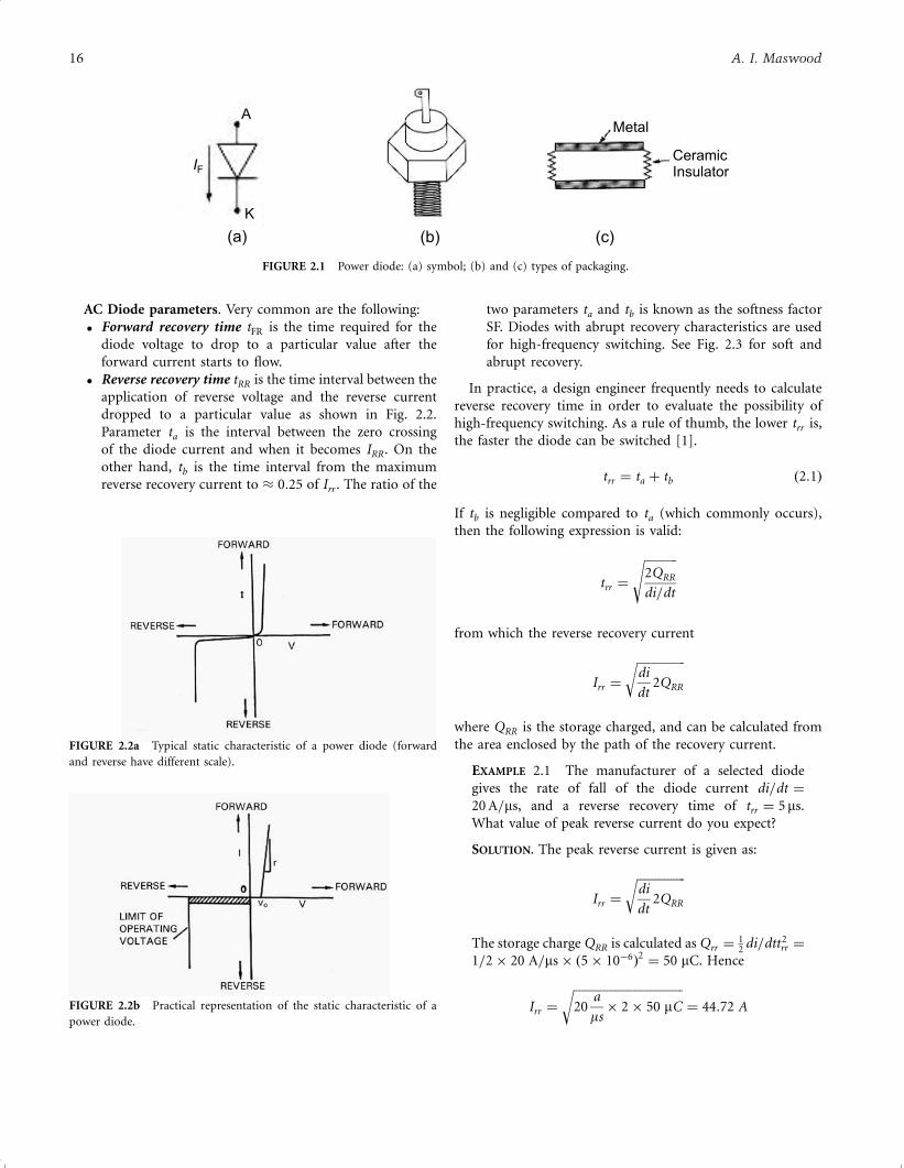
AC Diode parameters. Very common are the following:
� Forward recovery time tFR is the time required for the
diode voltage to drop to a particular value after the
forward current starts to flow.
� Reverse recovery time tRR is the time interval between the
application of reverse voltage and the reverse current
dropped to a particular value as shown in Fig. 2.2.
Parameter ta is the interval between the zero crossing
of the diode current and when it becomes IRR. On the
other hand, tb is the time interval from the maximum
reverse recovery current to � 0:25 of Irr . The ratio of the
two parameters ta and tb is known as the softness factor
SF. Diodes with abrupt recovery characteristics are used
for high-frequency switching. See Fig. 2.3 for soft and
abrupt recovery.
In practice, a design engineer frequently needs to calculate
reverse recovery time in order to evaluate the possibility of
high-frequency switching. As a rule of thumb, the lower trr is,
the faster the diode can be switched [1].
trr ¼ ta þ tb ð2:1Þ
If tb is negligible compared to ta (which commonly occurs),
then the following expression is valid:
trr ¼
�����������2QRR
di=dt
s
from which the reverse recovery current
Irr ¼
����������������di
dt2QRR
rwhere QRR is the storage charged, and can be calculated from
the area enclosed by the path of the recovery current.
EXAMPLE 2.1 The manufacturer of a selected diode
gives the rate of fall of the diode current di=dt ¼
20 A=ms, and a reverse recovery time of trr ¼ 5ms.
What value of peak reverse current do you expect?
SOLUTION. The peak reverse current is given as:
Irr ¼
����������������di
dt2QRR
rThe storage charge QRR is calculated as Qrr ¼
12
di=dtt2rr ¼
1=2� 20 A=ms� ð5� 10ÿ6Þ2¼ 50 mC. Hence
Irr ¼
������������������������������������20
a
ms� 2� 50 mC
r¼ 44:72 AFIGURE 2.2b Practical representation of the static characteristic of a
power diode.
FIGURE 2.2a Typical static characteristic of a power diode (forward
and reverse have different scale).
(a) (b) (c)
A
IF
K
Metal
CeramicInsulator
FIGURE 2.1 Power diode: (a) symbol; (b) and (c) types of packaging.
16 A. I. Maswood
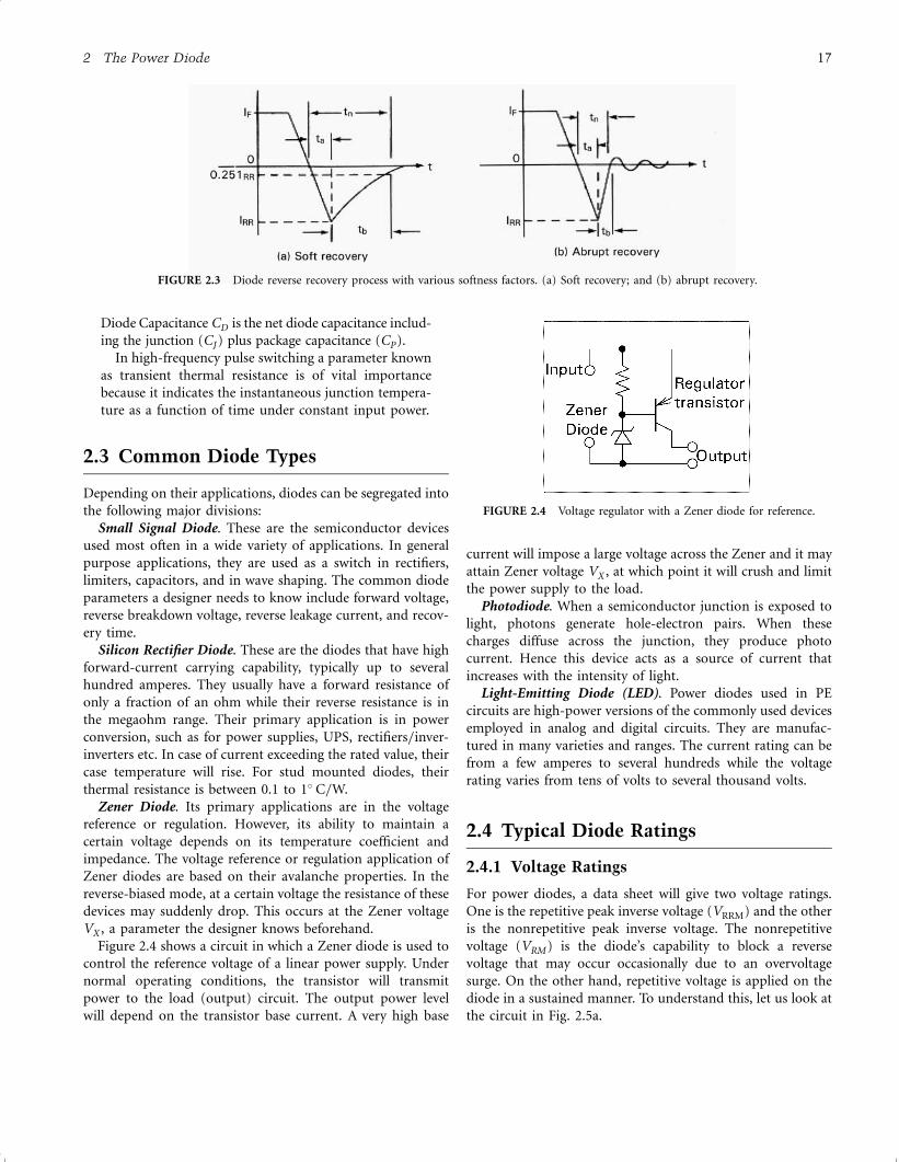
Diode Capacitance CD is the net diode capacitance includ-
ing the junction (CJ ) plus package capacitance (CP).
In high-frequency pulse switching a parameter known
as transient thermal resistance is of vital importance
because it indicates the instantaneous junction tempera-
ture as a function of time under constant input power.
2.3 Common Diode Types
Depending on their applications, diodes can be segregated into
the following major divisions:
Small Signal Diode. These are the semiconductor devices
used most often in a wide variety of applications. In general
purpose applications, they are used as a switch in rectifiers,
limiters, capacitors, and in wave shaping. The common diode
parameters a designer needs to know include forward voltage,
reverse breakdown voltage, reverse leakage current, and recov-
ery time.
Silicon Rectifier Diode. These are the diodes that have high
forward-current carrying capability, typically up to several
hundred amperes. They usually have a forward resistance of
only a fraction of an ohm while their reverse resistance is in
the megaohm range. Their primary application is in power
conversion, such as for power supplies, UPS, rectifiers=inver-
inverters etc. In case of current exceeding the rated value, their
case temperature will rise. For stud mounted diodes, their
thermal resistance is between 0.1 to 1� C=W.
Zener Diode. Its primary applications are in the voltage
reference or regulation. However, its ability to maintain a
certain voltage depends on its temperature coefficient and
impedance. The voltage reference or regulation application of
Zener diodes are based on their avalanche properties. In the
reverse-biased mode, at a certain voltage the resistance of these
devices may suddenly drop. This occurs at the Zener voltage
VX , a parameter the designer knows beforehand.
Figure 2.4 shows a circuit in which a Zener diode is used to
control the reference voltage of a linear power supply. Under
normal operating conditions, the transistor will transmit
power to the load (output) circuit. The output power level
will depend on the transistor base current. A very high base
current will impose a large voltage across the Zener and it may
attain Zener voltage VX , at which point it will crush and limit
the power supply to the load.
Photodiode. When a semiconductor junction is exposed to
light, photons generate hole-electron pairs. When these
charges diffuse across the junction, they produce photo
current. Hence this device acts as a source of current that
increases with the intensity of light.
Light-Emitting Diode (LED). Power diodes used in PE
circuits are high-power versions of the commonly used devices
employed in analog and digital circuits. They are manufac-
tured in many varieties and ranges. The current rating can be
from a few amperes to several hundreds while the voltage
rating varies from tens of volts to several thousand volts.
2.4 Typical Diode Ratings
2.4.1 Voltage Ratings
For power diodes, a data sheet will give two voltage ratings.
One is the repetitive peak inverse voltage (VRRM) and the other
is the nonrepetitive peak inverse voltage. The nonrepetitive
voltage (VRM ) is the diode’s capability to block a reverse
voltage that may occur occasionally due to an overvoltage
surge. On the other hand, repetitive voltage is applied on the
diode in a sustained manner. To understand this, let us look at
the circuit in Fig. 2.5a.
FIGURE 2.3 Diode reverse recovery process with various softness factors. (a) Soft recovery; and (b) abrupt recovery.
FIGURE 2.4 Voltage regulator with a Zener diode for reference.
2 The Power Diode 17
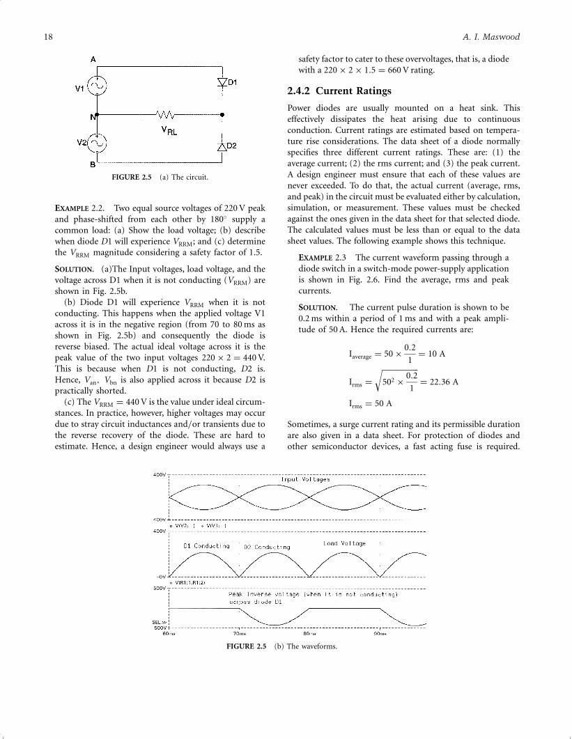
EXAMPLE 2.2. Two equal source voltages of 220 V peak
and phase-shifted from each other by 180� supply a
common load: (a) Show the load voltage; (b) describe
when diode D1 will experience VRRM; and (c) determine
the VRRM magnitude considering a safety factor of 1.5.
SOLUTION. (a)The Input voltages, load voltage, and the
voltage across D1 when it is not conducting (VRRM) are
shown in Fig. 2.5b.
(b) Diode D1 will experience VRRM when it is not
conducting. This happens when the applied voltage V1
across it is in the negative region (from 70 to 80 ms as
shown in Fig. 2.5b) and consequently the diode is
reverse biased. The actual ideal voltage across it is the
peak value of the two input voltages 220� 2 ¼ 440 V.
This is because when D1 is not conducting, D2 is.
Hence, Van; Vbn is also applied across it because D2 is
practically shorted.
(c) The VRRM ¼ 440 V is the value under ideal circum-
stances. In practice, however, higher voltages may occur
due to stray circuit inductances and=or transients due to
the reverse recovery of the diode. These are hard to
estimate. Hence, a design engineer would always use a
safety factor to cater to these overvoltages, that is, a diode
with a 220� 2� 1:5 ¼ 660 V rating.
2.4.2 Current Ratings
Power diodes are usually mounted on a heat sink. This
effectively dissipates the heat arising due to continuous
conduction. Current ratings are estimated based on tempera-
ture rise considerations. The data sheet of a diode normally
specifies three different current ratings. These are: (1) the
average current; (2) the rms current; and (3) the peak current.
A design engineer must ensure that each of these values are
never exceeded. To do that, the actual current (average, rms,
and peak) in the circuit must be evaluated either by calculation,
simulation, or measurement. These values must be checked
against the ones given in the data sheet for that selected diode.
The calculated values must be less than or equal to the data
sheet values. The following example shows this technique.
EXAMPLE 2.3 The current waveform passing through a
diode switch in a switch-mode power-supply application
is shown in Fig. 2.6. Find the average, rms and peak
currents.
SOLUTION. The current pulse duration is shown to be
0.2 ms within a period of 1 ms and with a peak ampli-
tude of 50 A. Hence the required currents are:
Iaverage ¼ 50�0:2
1¼ 10 A
Irms ¼
�������������������502 �
0:2
1
r¼ 22:36 A
Irms ¼ 50 A
Sometimes, a surge current rating and its permissible duration
are also given in a data sheet. For protection of diodes and
other semiconductor devices, a fast acting fuse is required.
FIGURE 2.5 (a) The circuit.
FIGURE 2.5 (b) The waveforms.
18 A. I. Maswood
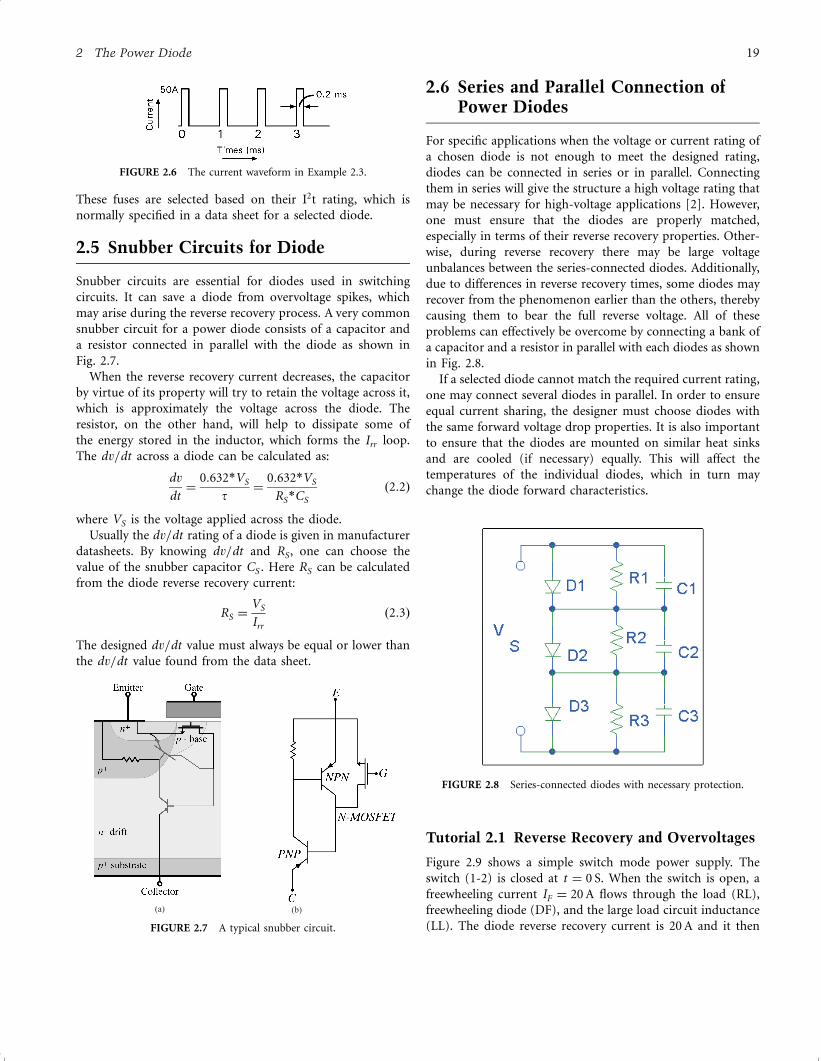
These fuses are selected based on their I2t rating, which is
normally specified in a data sheet for a selected diode.
2.5 Snubber Circuits for Diode
Snubber circuits are essential for diodes used in switching
circuits. It can save a diode from overvoltage spikes, which
may arise during the reverse recovery process. A very common
snubber circuit for a power diode consists of a capacitor and
a resistor connected in parallel with the diode as shown in
Fig. 2.7.
When the reverse recovery current decreases, the capacitor
by virtue of its property will try to retain the voltage across it,
which is approximately the voltage across the diode. The
resistor, on the other hand, will help to dissipate some of
the energy stored in the inductor, which forms the Irr loop.
The dv=dt across a diode can be calculated as:
dv
dt¼
0:632*VS
t¼
0:632*VS
RS*CS
ð2:2Þ
where VS is the voltage applied across the diode.
Usually the dv=dt rating of a diode is given in manufacturer
datasheets. By knowing dv=dt and RS , one can choose the
value of the snubber capacitor CS . Here RS can be calculated
from the diode reverse recovery current:
RS ¼VS
Irr
ð2:3Þ
The designed dv=dt value must always be equal or lower than
the dv=dt value found from the data sheet.
2.6 Series and Parallel Connection ofPower Diodes
For specific applications when the voltage or current rating of
a chosen diode is not enough to meet the designed rating,
diodes can be connected in series or in parallel. Connecting
them in series will give the structure a high voltage rating that
may be necessary for high-voltage applications [2]. However,
one must ensure that the diodes are properly matched,
especially in terms of their reverse recovery properties. Other-
wise, during reverse recovery there may be large voltage
unbalances between the series-connected diodes. Additionally,
due to differences in reverse recovery times, some diodes may
recover from the phenomenon earlier than the others, thereby
causing them to bear the full reverse voltage. All of these
problems can effectively be overcome by connecting a bank of
a capacitor and a resistor in parallel with each diodes as shown
in Fig. 2.8.
If a selected diode cannot match the required current rating,
one may connect several diodes in parallel. In order to ensure
equal current sharing, the designer must choose diodes with
the same forward voltage drop properties. It is also important
to ensure that the diodes are mounted on similar heat sinks
and are cooled (if necessary) equally. This will affect the
temperatures of the individual diodes, which in turn may
change the diode forward characteristics.
Tutorial 2.1 Reverse Recovery and Overvoltages
Figure 2.9 shows a simple switch mode power supply. The
switch (1-2) is closed at t ¼ 0 S. When the switch is open, a
freewheeling current IF ¼ 20 A flows through the load (RL),
freewheeling diode (DF), and the large load circuit inductance
(LL). The diode reverse recovery current is 20 A and it then
(a) (b)
FIGURE 2.7 A typical snubber circuit.
FIGURE 2.8 Series-connected diodes with necessary protection.
FIGURE 2.6 The current waveform in Example 2.3.
2 The Power Diode 19
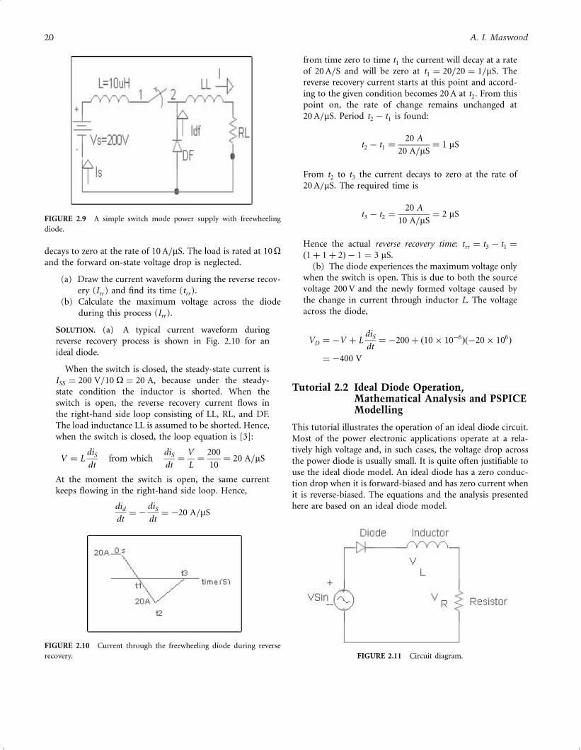
decays to zero at the rate of 10 A=mS. The load is rated at 10Oand the forward on-state voltage drop is neglected.
(a) Draw the current waveform during the reverse recov-
ery (Irr ) and find its time (trr ).
(b) Calculate the maximum voltage across the diode
during this process (Irr ).
SOLUTION. (a) A typical current waveform during
reverse recovery process is shown in Fig. 2.10 for an
ideal diode.
When the switch is closed, the steady-state current is
ISS ¼ 200 V=10 O ¼ 20 A, because under the steady-
state condition the inductor is shorted. When the
switch is open, the reverse recovery current flows in
the right-hand side loop consisting of LL, RL, and DF.
The load inductance LL is assumed to be shorted. Hence,
when the switch is closed, the loop equation is [3]:
V ¼ LdiS
dtfrom which
diS
dt¼
V
L¼
200
10¼ 20 A=mS
At the moment the switch is open, the same current
keeps flowing in the right-hand side loop. Hence,
did
dt¼ ÿ
diS
dt¼ ÿ20 A=mS
from time zero to time t1 the current will decay at a rate
of 20 A=S and will be zero at t1 ¼ 20=20 ¼ 1=mS. The
reverse recovery current starts at this point and accord-
ing to the given condition becomes 20 A at t2. From this
point on, the rate of change remains unchanged at
20 A=mS. Period t2 ÿ t1 is found:
t2 ÿ t1 ¼20 A
20 A=mS¼ 1 mS
From t2 to t3 the current decays to zero at the rate of
20 A=mS. The required time is
t3 ÿ t2 ¼20 A
10 A=mS¼ 2 mS
Hence the actual reverse recovery time: trr ¼ t3 ÿ t1 ¼
ð1þ 1þ 2Þ ÿ 1 ¼ 3 mS.
(b) The diode experiences the maximum voltage only
when the switch is open. This is due to both the source
voltage 200 V and the newly formed voltage caused by
the change in current through inductor L. The voltage
across the diode,
VD ¼ ÿV þ LdiS
dt¼ ÿ200þ ð10� 10ÿ6Þðÿ20� 106Þ
¼ ÿ400 V
Tutorial 2.2 Ideal Diode Operation,Mathematical Analysis and PSPICEModelling
This tutorial illustrates the operation of an ideal diode circuit.
Most of the power electronic applications operate at a rela-
tively high voltage and, in such cases, the voltage drop across
the power diode is usually small. It is quite often justifiable to
use the ideal diode model. An ideal diode has a zero conduc-
tion drop when it is forward-biased and has zero current when
it is reverse-biased. The equations and the analysis presented
here are based on an ideal diode model.
FIGURE 2.9 A simple switch mode power supply with freewheeling
diode.
FIGURE 2.10 Current through the freewheeling diode during reverse
recovery. FIGURE 2.11 Circuit diagram.
20 A. I. Maswood
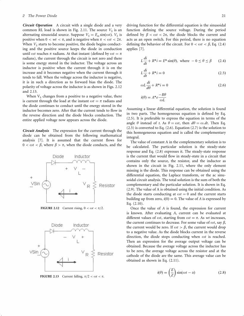
Circuit Operation A circuit with a single diode and a very
common RL load is shown in Fig. 2.11. The source VS is an
alternating sinusoidal source. Suppose VS ¼ Em sinðotÞ. VS is
positive when 0 < wt < p, and is negative when p < ot < 2p.
When VS starts to become positive, the diode begins conduct-
ing and the positive source keeps the diode in conduction
until ot reaches p radians. At that instant (defined by ot ¼ pradians), the current through the circuit is not zero and there
is some energy stored in the inductor. The voltage across an
inductor is positive when the current through it is on the
increase and it becomes negative when the current through it
tends to fall. When the voltage across the inductor is negative,
it is in such a direction as to forward bias the diode. The
polarity of voltage across the inductor is as shown in Figs. 2.12
and 2.13.
When VS changes from a positive to a negative value, there
is current through the load at the instant ot ¼ p radians and
the diode continues to conduct until the energy stored in the
inductor becomes zero. After that the current tends to flow in
the reverse direction and the diode blocks conduction. The
entire applied voltage now appears across the diode.
Circuit Analysis The expression for the current through the
diode can be obtained from the following mathematical
analysis [7]. It is assumed that the current flows for
0 < ot < b, where b > p, when the diode conducts, and the
driving function for the differential equation is the sinusoidal
function defining the source voltage. During the period
defined by b < ot < 2p, the diode blocks the current and
acts as an open switch. For this period, there is no equation
defining the behavior of the circuit. For 0 < ot < b, Eq. (2.4)
applies [7].
Ldi
dtþ R*i ¼ E* sinðyÞ; where ÿ 0 � y � b ð2:4Þ
Ldi
dtþ R*i ¼ 0 ð2:5Þ
oLdi
dyþ R*i ¼ 0 ð2:6Þ
iðyÞ ¼ A*eÿRyoL
Assuming a linear differential equation, the solution is found
in two parts. The homogeneous equation is defined by Eq.
(2.5). It is preferable to express the equation in terms of the
angle y instead of t. As y ¼ ot , then dy ¼ o:dt . Then Eq.
(2.5) is converted to Eq. (2.6). Equation (2.7) is the solution to
this homogeneous equation and is called the complementary
integral.
The value of constant A in the complementary solution is to
be calculated. The particular solution is the steady-state
response and Eq. (2.8) expresses it. The steady-state response
is the current that would flow in steady-state in a circuit that
contains only the source, the resistor, and the inductor as
shown in the circuit in Fig. 2.11, where the only element
missing is the diode. This response can be obtained using the
differential equation, the Laplace transform, or the ac sinu-
soidal circuit analysis. The total solution is the sum of both the
complementary and the particular solution. It is shown in Eq.
(2.9). The value of A is obtained using the initial condition. As
the diode starts conducting at ot ¼ 0 and the current starts
building up from zero, ið0Þ ¼ 0. The value of A is expressed by
Eq. (2.10).
Once the value of A is found, the expression for current
is known. After evaluating A, current can be evaluated at
different values of ot , starting from ot ¼ p. As wt increases,
the current continues to decrease. For some value of ot , say b,
the current would be zero. If ot > b, the current would drop
to a negative value. As the diode blocks current in the reverse
direction, the diode stops conducting when ot is reached.
Then an expression for the average output voltage can be
obtained. Because the average voltage across the inductor has
to be zero, the average voltage across the resistor and at the
cathode of the diode are the same. This average value can be
obtained as shown in Eq. (2.11).
iðyÞ ¼E
Z
� �sinðot ÿ aÞ ð2:8Þ
FIGURE 2.12 Current rising, 0 < ot < p=2:
FIGURE 2.13 Current falling, p=2 < ot < p.
2 The Power Diode 21
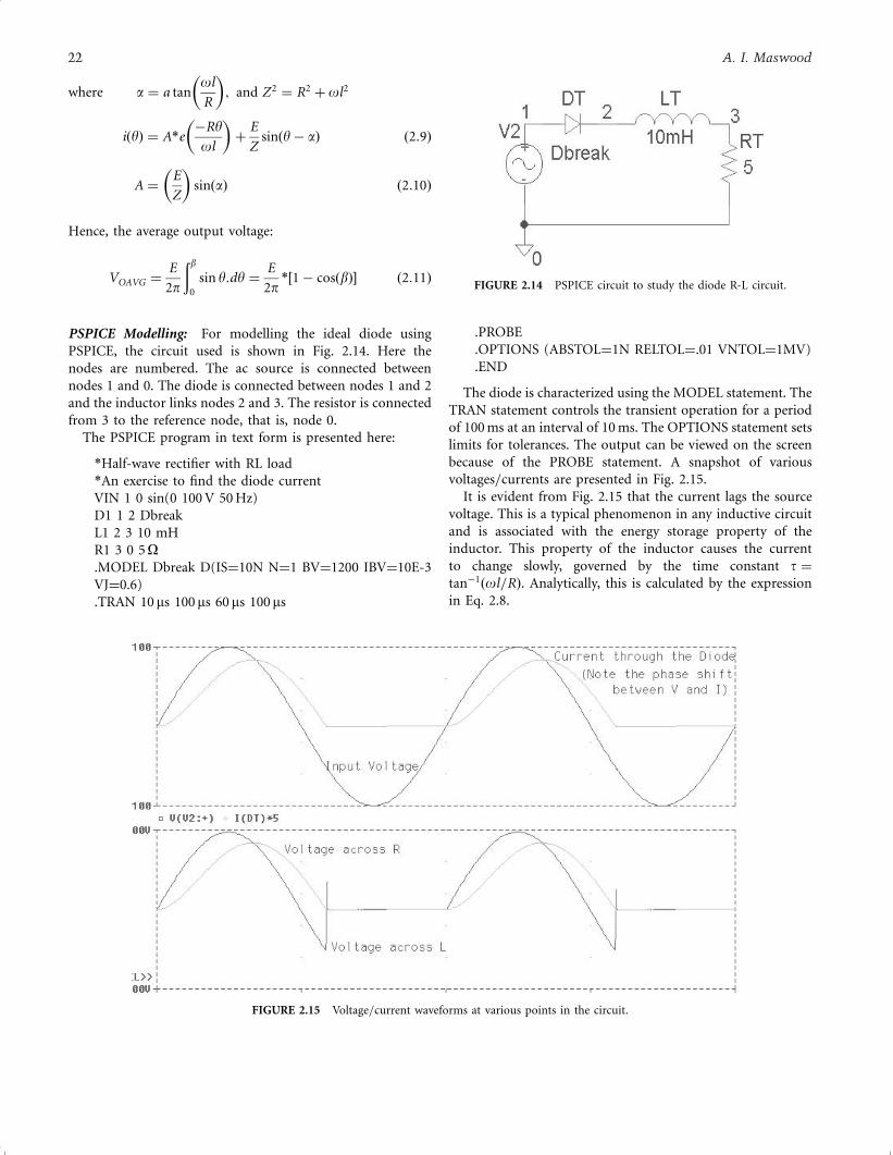
where a ¼ a tanol
R
� �; and Z2 ¼ R2 þ ol2
iðyÞ ¼ A*eÿRyol
� �þ
E
Zsinðyÿ aÞ ð2:9Þ
A ¼E
Z
� �sinðaÞ ð2:10Þ
Hence, the average output voltage:
VOAVG ¼E
2p
ðb0
sin y:dy ¼E
2p*�1ÿ cosðbÞ� ð2:11Þ
PSPICE Modelling: For modelling the ideal diode using
PSPICE, the circuit used is shown in Fig. 2.14. Here the
nodes are numbered. The ac source is connected between
nodes 1 and 0. The diode is connected between nodes 1 and 2
and the inductor links nodes 2 and 3. The resistor is connected
from 3 to the reference node, that is, node 0.
The PSPICE program in text form is presented here:
*Half-wave rectifier with RL load
*An exercise to find the diode current
VIN 1 0 sin(0 100 V 50 Hz)
D1 1 2 Dbreak
L1 2 3 10 mH
R1 3 0 5O.MODEL Dbreak D(IS¼10N N¼1 BV¼1200 IBV¼10E-3
VJ¼0.6)
.TRAN 10 ms 100 ms 60 ms 100 ms
.PROBE
.OPTIONS (ABSTOL¼1N RELTOL¼.01 VNTOL¼1MV)
.END
The diode is characterized using the MODEL statement. The
TRAN statement controls the transient operation for a period
of 100 ms at an interval of 10 ms. The OPTIONS statement sets
limits for tolerances. The output can be viewed on the screen
because of the PROBE statement. A snapshot of various
voltages=currents are presented in Fig. 2.15.
It is evident from Fig. 2.15 that the current lags the source
voltage. This is a typical phenomenon in any inductive circuit
and is associated with the energy storage property of the
inductor. This property of the inductor causes the current
to change slowly, governed by the time constant t ¼tanÿ1ðol=RÞ. Analytically, this is calculated by the expression
in Eq. 2.8.
FIGURE 2.14 PSPICE circuit to study the diode R-L circuit.
FIGURE 2.15 Voltage=current waveforms at various points in the circuit.
22 A. I. Maswood
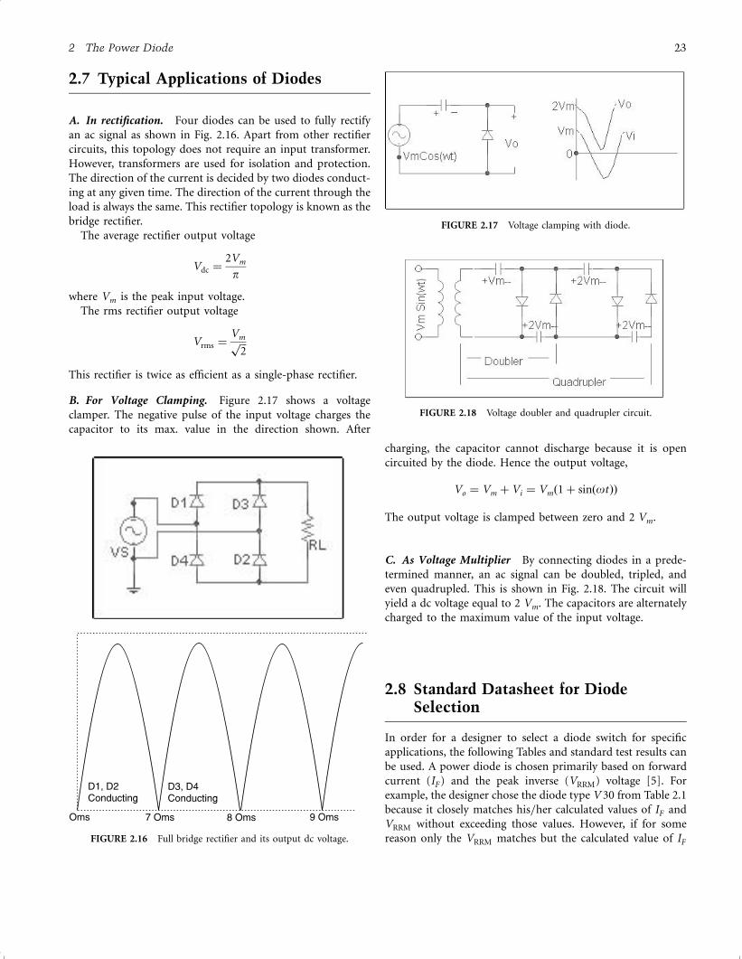
2.7 Typical Applications of Diodes
A. In rectification. Four diodes can be used to fully rectify
an ac signal as shown in Fig. 2.16. Apart from other rectifier
circuits, this topology does not require an input transformer.
However, transformers are used for isolation and protection.
The direction of the current is decided by two diodes conduct-
ing at any given time. The direction of the current through the
load is always the same. This rectifier topology is known as the
bridge rectifier.
The average rectifier output voltage
Vdc ¼2Vm
p
where Vm is the peak input voltage.
The rms rectifier output voltage
Vrms ¼Vm���
2p
This rectifier is twice as efficient as a single-phase rectifier.
B. For Voltage Clamping. Figure 2.17 shows a voltage
clamper. The negative pulse of the input voltage charges the
capacitor to its max. value in the direction shown. After
charging, the capacitor cannot discharge because it is open
circuited by the diode. Hence the output voltage,
Vo ¼ Vm þ Vi ¼ Vmð1þ sinðotÞÞ
The output voltage is clamped between zero and 2 Vm.
C. As Voltage Multiplier By connecting diodes in a prede-
termined manner, an ac signal can be doubled, tripled, and
even quadrupled. This is shown in Fig. 2.18. The circuit will
yield a dc voltage equal to 2 Vm. The capacitors are alternately
charged to the maximum value of the input voltage.
2.8 Standard Datasheet for DiodeSelection
In order for a designer to select a diode switch for specific
applications, the following Tables and standard test results can
be used. A power diode is chosen primarily based on forward
current (IF ) and the peak inverse (VRRM) voltage [5]. For
example, the designer chose the diode type V 30 from Table 2.1
because it closely matches his=her calculated values of IF and
VRRM without exceeding those values. However, if for some
reason only the VRRM matches but the calculated value of IF
FIGURE 2.17 Voltage clamping with diode.
FIGURE 2.18 Voltage doubler and quadrupler circuit.
FIGURE 2.16 Full bridge rectifier and its output dc voltage.
D1, D2Conducting
D3, D4Conducting
Oms 7 Oms 8 Oms 9 Oms
2 The Power Diode 23
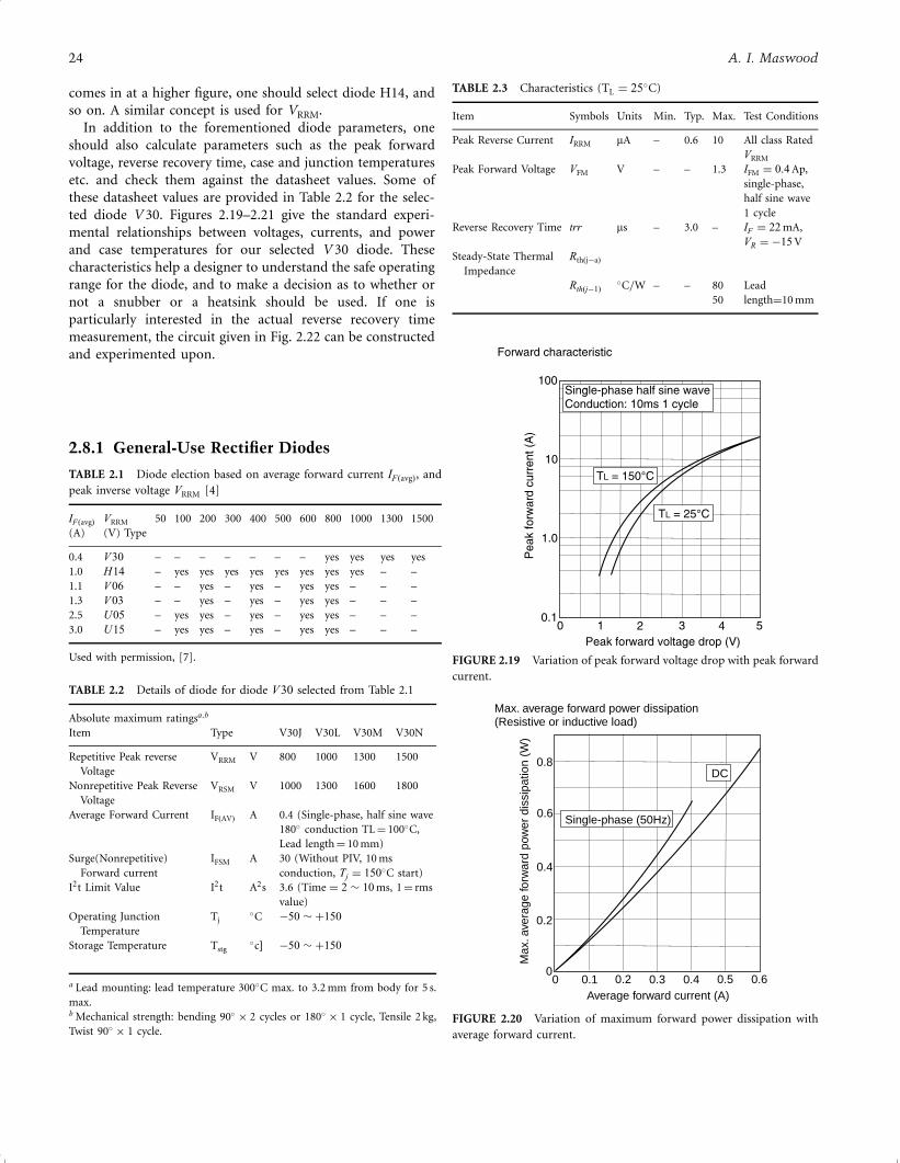
comes in at a higher figure, one should select diode H14, and
so on. A similar concept is used for VRRM.
In addition to the forementioned diode parameters, one
should also calculate parameters such as the peak forward
voltage, reverse recovery time, case and junction temperatures
etc. and check them against the datasheet values. Some of
these datasheet values are provided in Table 2.2 for the selec-
ted diode V 30. Figures 2.19–2.21 give the standard experi-
mental relationships between voltages, currents, and power
and case temperatures for our selected V 30 diode. These
characteristics help a designer to understand the safe operating
range for the diode, and to make a decision as to whether or
not a snubber or a heatsink should be used. If one is
particularly interested in the actual reverse recovery time
measurement, the circuit given in Fig. 2.22 can be constructed
and experimented upon.
2.8.1 General-Use Rectifier Diodes
TABLE 2.1 Diode election based on average forward current IFðavgÞ, and
peak inverse voltage VRRM [4]
IFðavgÞ
(A)
VRRM
(V) Type
50 100 200 300 400 500 600 800 1000 1300 1500
0.4 V30 – – – – – – – yes yes yes yes
1.0 H14 – yes yes yes yes yes yes yes yes – –
1.1 V06 – – yes – yes – yes yes – – –
1.3 V03 – – yes – yes – yes yes – – –
2.5 U05 – yes yes – yes – yes yes – – –
3.0 U15 – yes yes – yes – yes yes – – –
Used with permission, [7].
TABLE 2.2 Details of diode for diode V 30 selected from Table 2.1
Absolute maximum ratingsa;b
Item Type V30J V30L V30M V30N
Repetitive Peak reverse
Voltage
VRRM V 800 1000 1300 1500
Nonrepetitive Peak Reverse
Voltage
VRSM V 1000 1300 1600 1800
Average Forward Current IFðAVÞ A 0.4 (Single-phase, half sine wave
180� conduction TL¼ 100�C,
Lead length¼ 10 mm)
Surge(Nonrepetitive)
Forward current
IFSM A 30 (Without PIV, 10 ms
conduction, Tj ¼ 150�C start)
I2t Limit Value I2t A2s 3.6 (Time ¼ 2 � 10 ms, 1¼ rms
value)
Operating Junction
Temperature
Tj�C ÿ50 � þ150
Storage Temperature Tstg�c� ÿ50 � þ150
a Lead mounting: lead temperature 300�C max. to 3.2 mm from body for 5 s.
max.b Mechanical strength: bending 90� � 2 cycles or 180� � 1 cycle, Tensile 2 kg,
Twist 90� � 1 cycle.
TABLE 2.3 Characteristics (TL ¼ 25�C)
Item Symbols Units Min. Typ. Max. Test Conditions
Peak Reverse Current IRRM mA – 0.6 10 All class Rated
VRRM
Peak Forward Voltage VFM V – – 1.3 IFM ¼ 0:4 Ap,
single-phase,
half sine wave
1 cycle
Reverse Recovery Time trr ms – 3.0 – IF ¼ 22 mA,
VR ¼ ÿ15 V
Steady-State Thermal
Impedance
RthðjÿaÞ
Rthðjÿ1Þ�C=W – – 80 Lead
50 length¼10 mm
0
100
Forward characteristic
Single-phase half sine waveConduction: 10ms 1 cycle
10
1.0
0.11 2 3 4 5
Peak forward voltage drop (V)
Pe
ak
forw
ard
cu
rre
nt(A
)
T = 150 CL °
T = 25 CL °
FIGURE 2.19 Variation of peak forward voltage drop with peak forward
current.
0
0.8
Max. average forward power dissipation(Resistive or inductive load)
0.6
0.4
00.1Average forward current (A)
Max
.ave
rage
forw
ard
pow
er d
issi
patio
n (W
)
DC
0.2
0.2 0.3 0.4 0.5 0.6
Single-phase (50Hz)
FIGURE 2.20 Variation of maximum forward power dissipation with
average forward current.
24 A. I. Maswood
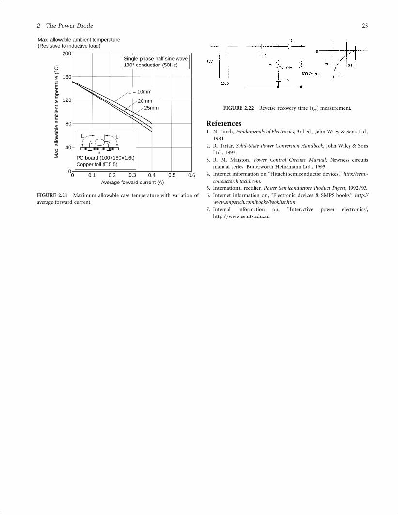
References1. N. Lurch, Fundamenals of Electronics, 3rd ed., John Wiley & Sons Ltd.,
1981.
2. R. Tartar, Solid-State Power Conversion Handbook, John Wiley & Sons
Ltd., 1993.
3. R. M. Marston, Power Control Circuits Manual, Newness circuits
manual series. Butterworth Heinemann Ltd., 1995.
4. Internet information on ‘‘Hitachi semiconductor devices,’’ http://semi-
conductor.hitachi.com.
5. International rectifier, Power Semiconductors Product Digest, 1992=93.
6. Internet information on, ‘‘Electronic devices & SMPS books,’’ http://
www.smpstech.com/books/booklist.htm
7. Internal information on, ‘‘Interactive power electronics’’,
http:==www.ee.uts.edu.au
0
160
Max. allowable ambient temperature(Resistive to inductive load)
120
80
00.1
Average forward current (A)
Max
.allo
wab
le a
mbi
ent t
empe
ratu
re (
C)
°
40
0.2 0.3 0.4 0.5 0.6
200Single-phase half sine wave180 conduction (50Hz)°
L = 10mm
PC board (100 180 1.6t)Copper foil ( 5.5)
× ×
LL
20mm25mm
FIGURE 2.21 Maximum allowable case temperature with variation of
average forward current.
FIGURE 2.22 Reverse recovery time (trr) measurement.
2 The Power Diode 25
3Thyristors
Jerry Hudgins, Ph.D.Enrico Santi, Ph.D.Antonio Caiafa, Ph.D.Katherine Lengel, Ph.D.Department of Electrical
Engineering
University of South Carolina
Columbia, South Carolina
29208 USA
Patrick R. Palmer, Ph.D.Department of Engineering
Cambridge University
Trumpington Street
Cambridge CB2 1PZ, United
Kingdom
3.1 Introduction
Thyristors are usually three-terminal devices with four layers
of alternating p- and n-type material (i.e. three p-n junctions)
in their main power handling section. In contrast to the linear
relation that exists between load and control currents in a
transistor, the thyristor is bistable. The control terminal of the
thyristor, called the gate (G) electrode, may be connected to an
integrated and complex structure as part of the device. The
other two terminals, anode (A) and cathode (K ), handle the
large applied potentials (often of both polarities) and conduct
the major current through the thyristor. The anode and
cathode terminals are connected in series with the load to
which power is to be controlled.
Thyristors are used to approximate ideal closed (no voltage
drop between anode and cathode) or open (no anode current
flow) switches for control of power flow in a circuit. This
differs from low-level digital switching circuits that are
designed to deliver two distinct small voltage levels while
conducting small currents (ideally zero). Power electronic
circuits must have the capability of delivering large currents
and be able to withstand large externally applied voltages. All
thyristor types are controllable in switching from a forward-
blocking state (positive potential applied to the anode with
respect to the cathode with correspondingly little anode
current flow) into a forward-conduction state (large forward
anode current flowing with a small anode-cathode potential
drop). After switching from a forward-blocking state into the
forward-conduction state, most thyristors have the character-
istic that the gate signal can be removed and the thyristor will
remain in its forward-conduction mode. This property,
termed ‘‘latching,’’ is an important distinction between
thyristors and other types of power electronic devices. Some
thyristors are also controllable in switching from forward-
conduction back to a forward-blocking state. The particular
design of a thyristor will determine its controllability and often
its application.
Thyristors are typically used at the highest energy levels in
power conditioning circuits because they are designed to
handle the largest currents and voltages of any device technol-
ogy (systems with voltages approximately greater than 1 kV or
currents higher than 100 A). Many medium-power circuits
(systems operating at <1 kV or 100 A) and particularly low-
power circuits (systems operating <100 V or several amperes)
Copyright # 2001 by Academic Press.
All rights of reproduction in any form reserved.
27
3.1 Introduction........................................................................................ 27
3.2 Basic Structure and Operation................................................................ 28
3.3 Static Characteristics ............................................................................. 303.3.1 Current-Voltage Curves for Thyristors � 3.3.2 Edge and Surface Terminations
� 3.3.3 Packaging
3.4 Dynamic Switching Characteristics.......................................................... 333.4.1 Cathode Shorts � 3.4.2 Anode Shorts � 3.4.3 Amplifying Gate � 3.4.4 Temperature
Dependencies
3.5 Thyristor Parameters............................................................................. 37
3.6 Types of Thyristors ............................................................................... 383.6.1 SCRs and GTOs � 3.6.2 MOS-Controlled Thyristors, MCT � 3.6.3 Static Induction
Thyristors � 3.6.4 Optically Triggered Thyristors � 3.6.5 Bidirectional Control Thyristor
3.7 Gate Drive Requirements....................................................................... 453.7.1 Snubber Circuits � 3.7.2 Gate Circuits
3.8 P-Spice Model ..................................................................................... 47
3.9 Applications ........................................................................................ 503.9.1 Direct current-Alternating current Utility Inverters � 3.9.2 Motor Control
� 3.9.3 VAR Compensators and Static Switching Systems
References ........................................................................................... 53
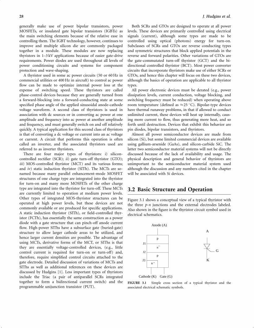
generally make use of power bipolar transistors, power
MOSFETs, or insulated gate bipolar transistors (IGBTs) as
the main switching elements because of the relative ease in
controlling them. The IGBT technology, however, continues to
improve and multiple silicon die are commonly packaged
together in a module. These modules are now replacing
thyristors in 1–3 kV applications because of easier gate-drive
requirements. Power diodes are used throughout all levels of
power conditioning circuits and systems for component
protection and wave-shaping.
A thyristor used in some ac power circuits (50 or 60 Hz in
commercial utilities or 400 Hz in aircraft) to control ac power
flow can be made to optimize internal power loss at the
expense of switching speed. These thyristors are called
phase-control devices because they are generally turned from
a forward-blocking into a forward-conducting state at some
specified phase angle of the applied sinusoidal anode-cathode
voltage waveform. A second class of thyristors is used in
association with dc sources or in converting ac power at one
amplitude and frequency into ac power at another amplitude
and frequency, and must generally switch on and off relatively
quickly. A typical application for this second class of thyristors
is that of converting a dc voltage or current into an ac voltage
or current. A circuit that performs this operation is often
called an inverter, and the associated thyristors used are
referred to as inverter thyristors.
There are four major types of thyristors: i) silicon-
controlled rectifier (SCR); ii) gate turn-off thyristor (GTO);
iii) MOS-controlled thyristor (MCT) and its various forms;
and iv) static induction thyristor (SITh). The MCTs are so-
named because many parallel enhancement-mode MOSFET
structures of one charge type are integrated into the thyristor
for turn-on and many more MOSFETs of the other charge
type are integrated into the thyristor for turn-off. These MCTs
are currently limited to operation at medium power levels.
Other types of integrated MOS-thyristor structures can be
operated at high power levels, but these devices are not
commonly available or are produced for specific applications.
A static induction thyristor (SITh), or field-controlled thyr-
istor (FCTh), has essentially the same construction as a power
diode with a gate structure that can pinch-off anode current
flow. High-power SIThs have a subsurface gate (buried-gate)
structure to allow larger cathode areas to be utilized, and
hence larger current densities are possible. The advantage of
using MCTs, derivative forms of the MCT, or SIThs is that
they are essentially voltage-controlled devices, (e.g., little
control current is required for turn-on or turn-off) and,
therefore, require simplified control circuits attached to the
gate electrode. Detailed discussion of variations of MCTs and
SIThs as well as additional references on these devices are
discussed by Hudgins [1]. Less important types of thyristors
include the Triac (a pair of antiparallel SCRs integrated
together to form a bidirectional current switch) and the
programmable unijunction transistor (PUT).
Both SCRs and GTOs are designed to operate at all power
levels. These devices are primarily controlled using electrical
signals (current), although some types are made to be
controlled using optical (photons) energy for turn-on.
Subclasses of SCRs and GTOs are reverse conducting types
and symmetric structures that block applied potentials in the
reverse and forward polarities. Other variations of GTOs are
the gate-commutated turn-off thyristor (GCT) and the bi-
directional controlled thyristor (BCT). Most power converter
circuits that incorporate thyristors make use of either SCRs or
GTOs, and hence this chapter will focus on these two devices,
although the basics of operation are applicable to all thyristor
types.
All power electronic devices must be derated (e.g., power
dissipation levels, current conduction, voltage blocking, and
switching frequency must be reduced) when operating above
room temperature (defined as �25 �C). Bipolar-type devices
have thermal runaway problems, in that if allowed to conduct
unlimited current, these devices will heat up internally, caus-
ing more current to flow, thus generating more heat, and so
forth until destruction. Devices that exhibit this behavior are
pin diodes, bipolar transistors, and thyristors.
Almost all power semiconductor devices are made from
silicon (Si), but some limited commercial devices are available
using gallium-arsenide (GaAs), and silicon-carbide SiC. The
latter two semiconductor material systems will not be directly
discussed because of the lack of availability and usage. The
physical description and general behavior of thyristors are
unimportant to the semiconductor material system used
although the discussion and any numbers cited in the chapter
will be associated with Si devices.
3.2 Basic Structure and Operation
Figure 3.1 shows a conceptual view of a typical thyristor with
the three p-n junctions and the external electrodes labeled.
Also shown in the figure is the thyristor circuit symbol used in
electrical schematics.
Anode (A)
Gate (G)Cathode (K)
J3
J1
J2
p
p
n-
n +
G
K
A
FIGURE 3.1 Simple cross section of a typical thyristor and the
associated electrical schematic symbols.
28 J. Hudgins et al.28 J. Hudgins et al.
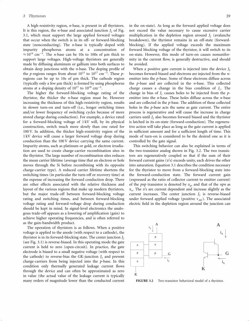
A high-resistivity region, n-base, is present in all thyristors.
It is this region, the n-base and associated junction J2 of Fig.
3.1, which must support the large applied forward voltages
that occur when the switch is in its off- or forward-blocking
state (nonconducting). The n-base is typically doped with
impurity phosphorus atoms at a concentration of
�1014 cmÿ3. The n-base can be 10s to 100s of mm thick to
support large voltages. High-voltage thyristors are generally
made by diffusing aluminum or gallium into both surfaces to
obtain deep junctions with the n-base. The doping profile of
the p-regions ranges from about 1015 to 1017 cmÿ3. These p-
regions can be up to 10s of mm thick. The cathode region
(typically only a few mm thick) is formed by using phosphorus
atoms at a doping density of 1017 to 1018 cmÿ3.
The higher the forward-blocking voltage rating of the
thyristor, the thicker the n-base region must be. However
increasing the thickness of this high-resistivity region, results
in slower turn-on and turn-off (i.e., longer switching times
and=or lower frequency of switching cycles because of more
stored charge during conduction). For example, a device rated
for a forward-blocking voltage of 1 kV will, by its physical
construction, switch much more slowly than one rated for
100 V. In addition, the thicker high-resistivity region of the
1 kV device will cause a larger forward voltage drop during
conduction than the 100 V device carrying the same current.
Impurity atoms, such as platinum or gold, or electron irradia-
tion are used to create charge-carrier recombination sites in
the thyristor. The large number of recombination sites reduces
the mean carrier lifetime (average time that an electron or hole
moves through the Si before recombining with its opposite
charge-carrier type). A reduced carrier lifetime shortens the
switching times (in particular the turn-off or recovery time) at
the expense of increasing the forward conduction drop. There
are other effects associated with the relative thickness and
layout of the various regions that make up modern thyristors,
but the major trade-off between forward-blocking voltage
rating and switching times, and between forward-blocking
voltage rating and forward-voltage drop during conduction
should be kept in mind. In signal-level electronics the analo-
gous trade-off appears as a lowering of amplification (gain) to
achieve higher operating frequencies, and is often referred to
as the gain-bandwidth product.
The operation of thyristors is as follows. When a positive
voltage is applied to the anode (with respect to a cathode), the
thyristor is in its forward-blocking state. The center junction J2
(see Fig. 3.1) is reverse-biased. In this operating mode the gate
current is held to zero (open-circuit). In practice, the gate
electrode is biased to a small negative voltage (with respect to
the cathode) to reverse-bias the GK-junction J3 and prevent
charge-carriers from being injected into the p-base. In this
condition only thermally generated leakage current flows
through the device and can often be approximated as zero
in value (the actual value of the leakage current is typically
many orders of magnitude lower than the conducted current
in the on-state). As long as the forward applied voltage does
not exceed the value necessary to cause excessive carrier
multiplication in the depletion region around J2 (avalanche
breakdown), the thyristor remains in an off-state (forward-
blocking). If the applied voltage exceeds the maximum
forward blocking voltage of the thyristor, it will switch to its
on-state. However, this mode of turn-on causes nonunifor-
mity in the current flow, is generally destructive, and should
be avoided.
When a positive gate current is injected into the device J3
becomes forward-biased and electrons are injected from the n-
emitter into the p-base. Some of these electrons diffuse across
the p-base and are collected in the n-base. This collected
charge causes a change in the bias condition of J1. The
change in bias of J1 causes holes to be injected from the p-
emitter into the n-base. These holes diffuse across the n-base
and are collected in the p-base. The addition of these collected
holes in the p-base acts the same as gate current. The entire
process is regenerative and will cause the increase in charge
carriers until J2 also becomes forward biased and the thyristor
is latched in its on-state (forward-conduction). The regenera-
tive action will take place as long as the gate current is applied
in sufficient amount and for a sufficient length of time. This
mode of turn-on is considered to be the desired one as it is
controlled by the gate signal.
This switching behavior can also be explained in terms of
the two-transistor analog shown in Fig. 3.2. The two transis-
tors are regeneratively coupled so that if the sum of their
forward current gains (a’s) exceeds unity, each drives the other
into saturation. Equation 3.1 describes the condition necessary
for the thyristor to move from a forward-blocking state into
the forward-conduction state. The forward current gain
(expressed as the ratio of collector current to emitter current)
of the pnp transistor is denoted by ap, and that of the npn as
an. The a’s are current dependent and increase slightly as the
current increases. The center junction J2 is reverse-biased
under forward applied voltage (positive nAK ). The associated
electric field in the depletion region around the junction can
iA
A
G
iG
K
p
n
p
n
n
p
iA
iG
A
G
K
FIGURE 3.2 Two-transistor behavioral model of a thyristor.
3 Thyristors 29
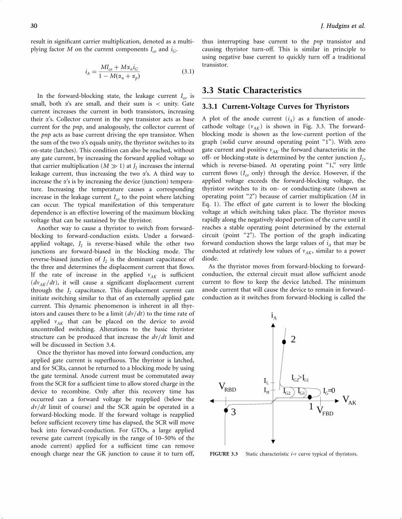
result in significant carrier multiplication, denoted as a multi-
plying factor M on the current components Ico and iG .
iA ¼MIco þManiG
1ÿMðan þ apÞð3:1Þ
In the forward-blocking state, the leakage current Ico is
small, both a’s are small, and their sum is < unity. Gate
current increases the current in both transistors, increasing
their a’s. Collector current in the npn transistor acts as base
current for the pnp, and analogously, the collector current of
the pnp acts as base current driving the npn transistor. When
the sum of the two a’s equals unity, the thyristor switches to its
on-state (latches). This condition can also be reached, without
any gate current, by increasing the forward applied voltage so
that carrier multiplication (M � 1) at J2 increases the internal
leakage current, thus increasing the two a’s. A third way to
increase the a’s is by increasing the device (junction) tempera-
ture. Increasing the temperature causes a corresponding
increase in the leakage current Ico to the point where latching
can occur. The typical manifestation of this temperature
dependence is an effective lowering of the maximum blocking
voltage that can be sustained by the thyristor.
Another way to cause a thyristor to switch from forward-
blocking to forward-conduction exists. Under a forward-
applied voltage, J2 is reverse-biased while the other two
junctions are forward-biased in the blocking mode. The
reverse-biased junction of J2 is the dominant capacitance of
the three and determines the displacement current that flows.
If the rate of increase in the applied nAK is sufficient
(dnAK=dt), it will cause a significant displacement current
through the J2 capacitance. This displacement current can
initiate switching similar to that of an externally applied gate
current. This dynamic phenomenon is inherent in all thyr-
istors and causes there to be a limit (dn=dt) to the time rate of
applied nAK that can be placed on the device to avoid
uncontrolled switching. Alterations to the basic thyristor
structure can be produced that increase the dn=dt limit and
will be discussed in Section 3.4.
Once the thyristor has moved into forward conduction, any
applied gate current is superfluous. The thyristor is latched,
and for SCRs, cannot be returned to a blocking mode by using
the gate terminal. Anode current must be commutated away
from the SCR for a sufficient time to allow stored charge in the
device to recombine. Only after this recovery time has
occurred can a forward voltage be reapplied (below the
dn=dt limit of course) and the SCR again be operated in a
forward-blocking mode. If the forward voltage is reapplied
before sufficient recovery time has elapsed, the SCR will move
back into forward-conduction. For GTOs, a large applied
reverse gate current (typically in the range of 10–50% of the
anode current) applied for a sufficient time can remove
enough charge near the GK junction to cause it to turn off,
thus interrupting base current to the pnp transistor and
causing thyristor turn-off. This is similar in principle to
using negative base current to quickly turn off a traditional
transistor.
3.3 Static Characteristics
3.3.1 Current-Voltage Curves for Thyristors
A plot of the anode current (iA) as a function of anode-
cathode voltage (nAK ) is shown in Fig. 3.3. The forward-
blocking mode is shown as the low-current portion of the
graph (solid curve around operating point ‘‘1’’). With zero
gate current and positive nAK the forward characteristic in the
off- or blocking-state is determined by the center junction J2,
which is reverse-biased. At operating point ‘‘1,’’ very little
current flows (Ico only) through the device. However, if the
applied voltage exceeds the forward-blocking voltage, the
thyristor switches to its on- or conducting-state (shown as
operating point ‘‘2") because of carrier multiplication (M in
Eq. 1). The effect of gate current is to lower the blocking
voltage at which switching takes place. The thyristor moves
rapidly along the negatively sloped portion of the curve until it
reaches a stable operating point determined by the external
circuit (point ‘‘2"). The portion of the graph indicating
forward conduction shows the large values of iA that may be
conducted at relatively low values of nAK , similar to a power
diode.
As the thyristor moves from forward-blocking to forward-
conduction, the external circuit must allow sufficient anode
current to flow to keep the device latched. The minimum
anode current that will cause the device to remain in forward-
conduction as it switches from forward-blocking is called the
iA
VFBD
IG=0
VAK1
2
3
VRBD IG2 IG1
IG2>IG1IL
IH
FIGURE 3.3 Static characteristic i-n curve typical of thyristors.
30 J. Hudgins et al.30 J. Hudgins et al.
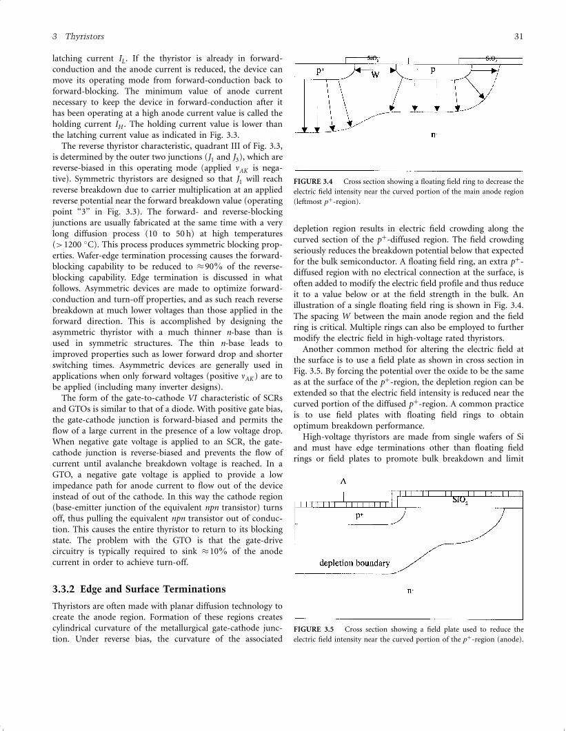
latching current IL. If the thyristor is already in forward-
conduction and the anode current is reduced, the device can
move its operating mode from forward-conduction back to
forward-blocking. The minimum value of anode current
necessary to keep the device in forward-conduction after it
has been operating at a high anode current value is called the
holding current IH . The holding current value is lower than
the latching current value as indicated in Fig. 3.3.
The reverse thyristor characteristic, quadrant III of Fig. 3.3,
is determined by the outer two junctions (J1 and J3), which are
reverse-biased in this operating mode (applied nAK is nega-
tive). Symmetric thyristors are designed so that J1 will reach
reverse breakdown due to carrier multiplication at an applied
reverse potential near the forward breakdown value (operating
point ‘‘3’’ in Fig. 3.3). The forward- and reverse-blocking
junctions are usually fabricated at the same time with a very
long diffusion process (10 to 50 h) at high temperatures
(>1200 �C). This process produces symmetric blocking prop-
erties. Wafer-edge termination processing causes the forward-
blocking capability to be reduced to �90% of the reverse-
blocking capability. Edge termination is discussed in what
follows. Asymmetric devices are made to optimize forward-
conduction and turn-off properties, and as such reach reverse
breakdown at much lower voltages than those applied in the
forward direction. This is accomplished by designing the
asymmetric thyristor with a much thinner n-base than is
used in symmetric structures. The thin n-base leads to
improved properties such as lower forward drop and shorter
switching times. Asymmetric devices are generally used in
applications when only forward voltages (positive nAK ) are to
be applied (including many inverter designs).
The form of the gate-to-cathode VI characteristic of SCRs
and GTOs is similar to that of a diode. With positive gate bias,
the gate-cathode junction is forward-biased and permits the
flow of a large current in the presence of a low voltage drop.
When negative gate voltage is applied to an SCR, the gate-
cathode junction is reverse-biased and prevents the flow of
current until avalanche breakdown voltage is reached. In a
GTO, a negative gate voltage is applied to provide a low
impedance path for anode current to flow out of the device
instead of out of the cathode. In this way the cathode region
(base-emitter junction of the equivalent npn transistor) turns
off, thus pulling the equivalent npn transistor out of conduc-
tion. This causes the entire thyristor to return to its blocking
state. The problem with the GTO is that the gate-drive
circuitry is typically required to sink �10% of the anode
current in order to achieve turn-off.
3.3.2 Edge and Surface Terminations
Thyristors are often made with planar diffusion technology to
create the anode region. Formation of these regions creates
cylindrical curvature of the metallurgical gate-cathode junc-
tion. Under reverse bias, the curvature of the associated
depletion region results in electric field crowding along the
curved section of the pþ-diffused region. The field crowding
seriously reduces the breakdown potential below that expected
for the bulk semiconductor. A floating field ring, an extra pþ-
diffused region with no electrical connection at the surface, is
often added to modify the electric field profile and thus reduce
it to a value below or at the field strength in the bulk. An
illustration of a single floating field ring is shown in Fig. 3.4.
The spacing W between the main anode region and the field
ring is critical. Multiple rings can also be employed to further
modify the electric field in high-voltage rated thyristors.
Another common method for altering the electric field at
the surface is to use a field plate as shown in cross section in
Fig. 3.5. By forcing the potential over the oxide to be the same
as at the surface of the pþ-region, the depletion region can be
extended so that the electric field intensity is reduced near the
curved portion of the diffused pþ-region. A common practice
is to use field plates with floating field rings to obtain
optimum breakdown performance.
High-voltage thyristors are made from single wafers of Si
and must have edge terminations other than floating field
rings or field plates to promote bulk breakdown and limit
FIGURE 3.4 Cross section showing a floating field ring to decrease the
electric field intensity near the curved portion of the main anode region
(leftmost pþ-region).
FIGURE 3.5 Cross section showing a field plate used to reduce the
electric field intensity near the curved portion of the pþ-region (anode).
3 Thyristors 31
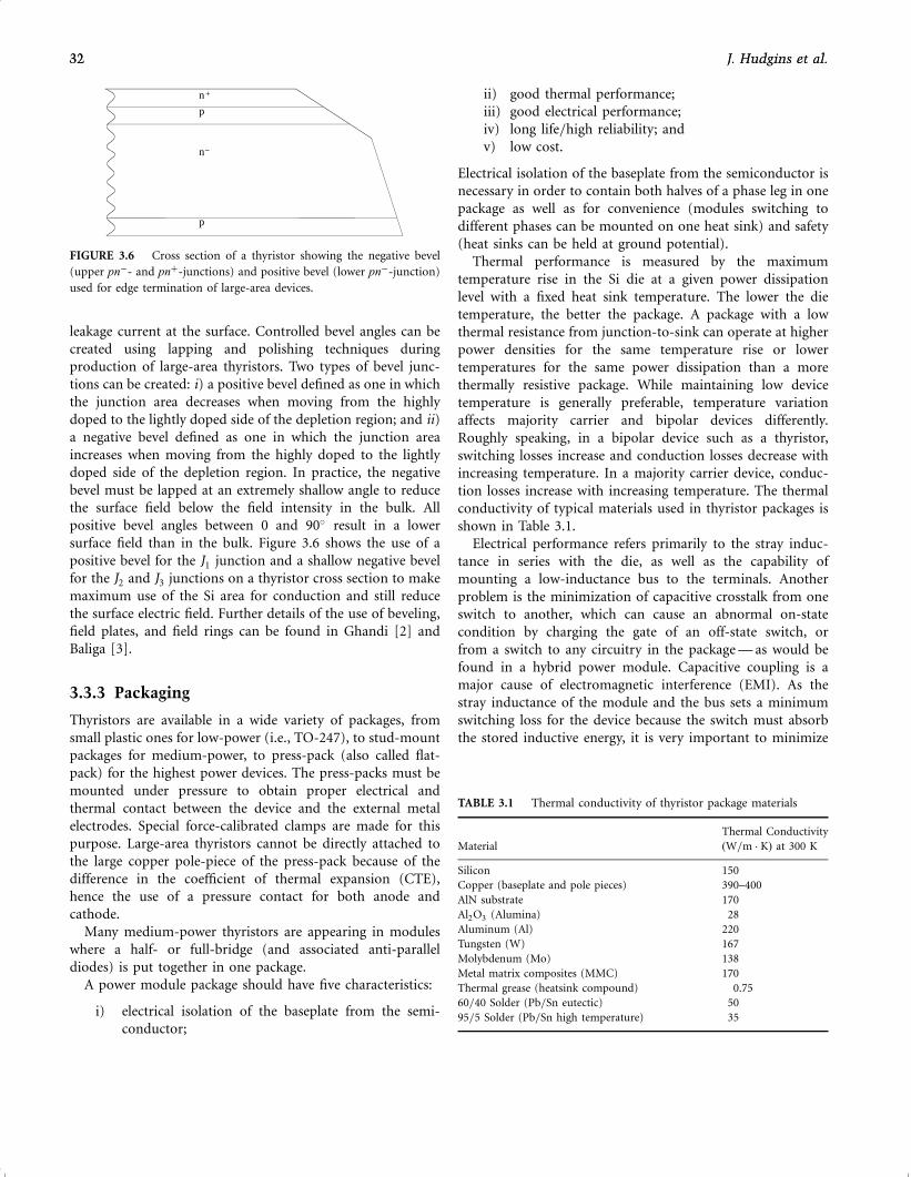
leakage current at the surface. Controlled bevel angles can be
created using lapping and polishing techniques during
production of large-area thyristors. Two types of bevel junc-
tions can be created: i) a positive bevel defined as one in which
the junction area decreases when moving from the highly
doped to the lightly doped side of the depletion region; and ii)
a negative bevel defined as one in which the junction area
increases when moving from the highly doped to the lightly
doped side of the depletion region. In practice, the negative
bevel must be lapped at an extremely shallow angle to reduce
the surface field below the field intensity in the bulk. All
positive bevel angles between 0 and 90� result in a lower
surface field than in the bulk. Figure 3.6 shows the use of a
positive bevel for the J1 junction and a shallow negative bevel
for the J2 and J3 junctions on a thyristor cross section to make
maximum use of the Si area for conduction and still reduce
the surface electric field. Further details of the use of beveling,
field plates, and field rings can be found in Ghandi [2] and
Baliga [3].
3.3.3 Packaging
Thyristors are available in a wide variety of packages, from
small plastic ones for low-power (i.e., TO-247), to stud-mount
packages for medium-power, to press-pack (also called flat-
pack) for the highest power devices. The press-packs must be
mounted under pressure to obtain proper electrical and
thermal contact between the device and the external metal
electrodes. Special force-calibrated clamps are made for this
purpose. Large-area thyristors cannot be directly attached to
the large copper pole-piece of the press-pack because of the
difference in the coefficient of thermal expansion (CTE),
hence the use of a pressure contact for both anode and
cathode.
Many medium-power thyristors are appearing in modules
where a half- or full-bridge (and associated anti-parallel
diodes) is put together in one package.
A power module package should have five characteristics:
i) electrical isolation of the baseplate from the semi-
conductor;
ii) good thermal performance;
iii) good electrical performance;
iv) long life=high reliability; and
v) low cost.
Electrical isolation of the baseplate from the semiconductor is
necessary in order to contain both halves of a phase leg in one
package as well as for convenience (modules switching to
different phases can be mounted on one heat sink) and safety
(heat sinks can be held at ground potential).
Thermal performance is measured by the maximum
temperature rise in the Si die at a given power dissipation
level with a fixed heat sink temperature. The lower the die
temperature, the better the package. A package with a low
thermal resistance from junction-to-sink can operate at higher
power densities for the same temperature rise or lower
temperatures for the same power dissipation than a more
thermally resistive package. While maintaining low device
temperature is generally preferable, temperature variation
affects majority carrier and bipolar devices differently.
Roughly speaking, in a bipolar device such as a thyristor,
switching losses increase and conduction losses decrease with
increasing temperature. In a majority carrier device, conduc-
tion losses increase with increasing temperature. The thermal
conductivity of typical materials used in thyristor packages is
shown in Table 3.1.
Electrical performance refers primarily to the stray induc-
tance in series with the die, as well as the capability of
mounting a low-inductance bus to the terminals. Another
problem is the minimization of capacitive crosstalk from one
switch to another, which can cause an abnormal on-state
condition by charging the gate of an off-state switch, or
from a switch to any circuitry in the package — as would be
found in a hybrid power module. Capacitive coupling is a
major cause of electromagnetic interference (EMI). As the
stray inductance of the module and the bus sets a minimum
switching loss for the device because the switch must absorb
the stored inductive energy, it is very important to minimize
n+
p
n-
p
FIGURE 3.6 Cross section of a thyristor showing the negative bevel
(upper pnÿ- and pnþ-junctions) and positive bevel (lower pnÿ-junction)
used for edge termination of large-area devices.
TABLE 3.1 Thermal conductivity of thyristor package materials
Material
Thermal Conductivity
ðW=m � KÞ at 300 K
Silicon 150
Copper (baseplate and pole pieces) 390–400
AlN substrate 170
Al2O3 (Alumina) 28
Aluminum (Al) 220
Tungsten (W) 167
Molybdenum (Mo) 138
Metal matrix composites (MMC) 170
Thermal grease (heatsink compound) 0.75
60=40 Solder (Pb=Sn eutectic) 50
95=5 Solder (Pb=Sn high temperature) 35
32 J. Hudgins et al.32 J. Hudgins et al.
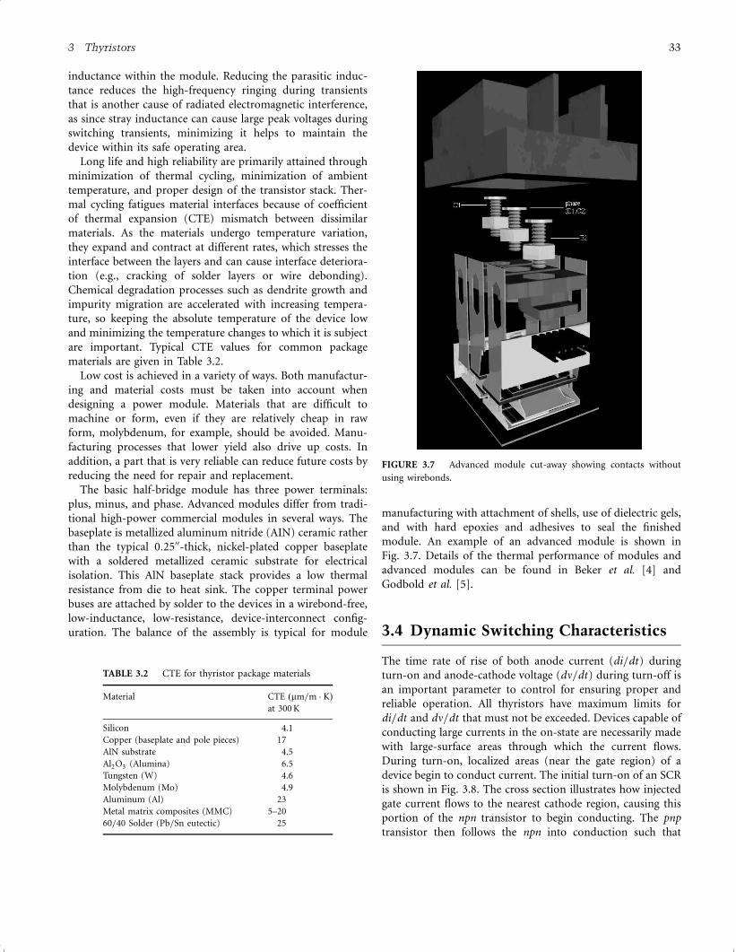
inductance within the module. Reducing the parasitic induc-
tance reduces the high-frequency ringing during transients
that is another cause of radiated electromagnetic interference,
as since stray inductance can cause large peak voltages during
switching transients, minimizing it helps to maintain the
device within its safe operating area.
Long life and high reliability are primarily attained through
minimization of thermal cycling, minimization of ambient
temperature, and proper design of the transistor stack. Ther-
mal cycling fatigues material interfaces because of coefficient
of thermal expansion (CTE) mismatch between dissimilar
materials. As the materials undergo temperature variation,
they expand and contract at different rates, which stresses the
interface between the layers and can cause interface deteriora-
tion (e.g., cracking of solder layers or wire debonding).
Chemical degradation processes such as dendrite growth and
impurity migration are accelerated with increasing tempera-
ture, so keeping the absolute temperature of the device low
and minimizing the temperature changes to which it is subject
are important. Typical CTE values for common package
materials are given in Table 3.2.
Low cost is achieved in a variety of ways. Both manufactur-
ing and material costs must be taken into account when
designing a power module. Materials that are difficult to
machine or form, even if they are relatively cheap in raw
form, molybdenum, for example, should be avoided. Manu-
facturing processes that lower yield also drive up costs. In
addition, a part that is very reliable can reduce future costs by
reducing the need for repair and replacement.
The basic half-bridge module has three power terminals:
plus, minus, and phase. Advanced modules differ from tradi-
tional high-power commercial modules in several ways. The
baseplate is metallized aluminum nitride (AIN) ceramic rather
than the typical 0:2500-thick, nickel-plated copper baseplate
with a soldered metallized ceramic substrate for electrical
isolation. This AlN baseplate stack provides a low thermal
resistance from die to heat sink. The copper terminal power
buses are attached by solder to the devices in a wirebond-free,
low-inductance, low-resistance, device-interconnect config-
uration. The balance of the assembly is typical for module
manufacturing with attachment of shells, use of dielectric gels,
and with hard epoxies and adhesives to seal the finished
module. An example of an advanced module is shown in
Fig. 3.7. Details of the thermal performance of modules and
advanced modules can be found in Beker et al. [4] and
Godbold et al. [5].
3.4 Dynamic Switching Characteristics
The time rate of rise of both anode current (di=dt) during
turn-on and anode-cathode voltage (dn=dt) during turn-off is
an important parameter to control for ensuring proper and
reliable operation. All thyristors have maximum limits for
di=dt and dn=dt that must not be exceeded. Devices capable of
conducting large currents in the on-state are necessarily made
with large-surface areas through which the current flows.
During turn-on, localized areas (near the gate region) of a
device begin to conduct current. The initial turn-on of an SCR
is shown in Fig. 3.8. The cross section illustrates how injected
gate current flows to the nearest cathode region, causing this
portion of the npn transistor to begin conducting. The pnp
transistor then follows the npn into conduction such that
TABLE 3.2 CTE for thyristor package materials
Material CTE ðmm=m � KÞ
at 300 K
Silicon 4.1
Copper (baseplate and pole pieces) 17
AlN substrate 4.5
Al2O3 (Alumina) 6.5
Tungsten (W) 4.6
Molybdenum (Mo) 4.9
Aluminum (Al) 23
Metal matrix composites (MMC) 5–20
60=40 Solder (Pb=Sn eutectic) 25
FIGURE 3.7 Advanced module cut-away showing contacts without
using wirebonds.
3 Thyristors 33
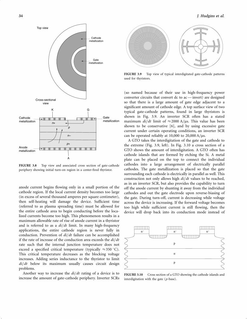
anode current begins flowing only in a small portion of the
cathode region. If the local current density becomes too large
(in excess of several thousand amperes per square centimeter),
then self-heating will damage the device. Sufficient time
(referred to as plasma spreading time) must be allowed for
the entire cathode area to begin conducting before the loca-
lized currents become too high. This phenomenon results in a
maximum allowable rate of rise of anode current in a thyristor
and is referred to as a di=dt limit. In many high-frequency
applications, the entire cathode region is never fully in
conduction. Prevention of di=dt failure can be accomplished
if the rate of increase of the conduction area exceeds the di=dt
rate such that the internal junction temperature does not
exceed a specified critical temperature (typically �350 �C).
This critical temperature decreases as the blocking voltage
increases. Adding series inductance to the thyristor to limit
di=dt below its maximum usually causes circuit design
problems.
Another way to increase the di=dt rating of a device is to
increase the amount of gate-cathode periphery. Inverter SCRs
(so named because of their use in high-frequency power
converter circuits that convert dc to ac — invert) are designed
so that there is a large amount of gate edge adjacent to a
significant amount of cathode edge. A top surface view of two
typical gate-cathode patterns, found in large thyristors is
shown in Fig. 3.9. An inverter SCR often has a stated
maximum di=dt limit of �2000 A=ms. This value has been
shown to be conservative [6], and by using excessive gate
current under certain operating conditions, an inverter SCR
can be operated reliably at 10,000 to 20,000 A=ms.
A GTO takes the interdigitation of the gate and cathode to
the extreme (Fig. 3.9, left). In Fig. 3.10 a cross section of a
GTO shows the amount of interdigitation. A GTO often has
cathode islands that are formed by etching the Si. A metal
plate can be placed on the top to connect the individual
cathodes into a large arrangement of electrically parallel
cathodes. The gate metallization is placed so that the gate
surrounding each cathode is electrically in parallel as well. This
construction not only allows high di=dt values to be reached,
as in an inverter SCR, but also provides the capability to turn
off the anode current by shunting it away from the individual
cathodes and out the gate electrode upon reverse-biasing of
the gate. During turn-off, current is decreasing while voltage
across the device is increasing. If the forward voltage becomes
too high while sufficient current is still flowing, then the
device will drop back into its conduction mode instead of
K
Cross-sectionalview
Cathodemetallization
n+
p
G
Gatemetallization
p+
n–
A
Anodemetallization
Top view
Cathodemetallization
Gatemetallization
FIGURE 3.8 Top view and associated cross section of gate-cathode
periphery showing initial turn-on region in a center-fired thyristor.
FIGURE 3.9 Top view of typical interdigitated gate-cathode patterns
used for thyristors.
n+ n+ n+
p
n-
p
FIGURE 3.10 Cross section of a GTO showing the cathode islands and
interdigitation with the gate (p-base).
34 J. Hudgins et al.34 J. Hudgins et al.
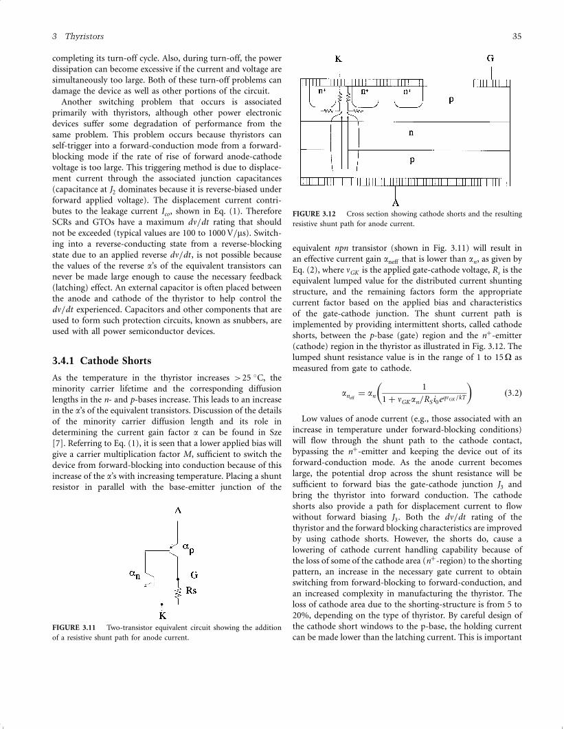
completing its turn-off cycle. Also, during turn-off, the power
dissipation can become excessive if the current and voltage are
simultaneously too large. Both of these turn-off problems can
damage the device as well as other portions of the circuit.
Another switching problem that occurs is associated
primarily with thyristors, although other power electronic
devices suffer some degradation of performance from the
same problem. This problem occurs because thyristors can
self-trigger into a forward-conduction mode from a forward-
blocking mode if the rate of rise of forward anode-cathode
voltage is too large. This triggering method is due to displace-
ment current through the associated junction capacitances
(capacitance at J2 dominates because it is reverse-biased under
forward applied voltage). The displacement current contri-
butes to the leakage current Ico, shown in Eq. (1). Therefore
SCRs and GTOs have a maximum dn=dt rating that should
not be exceeded (typical values are 100 to 1000 V=ms). Switch-
ing into a reverse-conducting state from a reverse-blocking
state due to an applied reverse dn=dt , is not possible because
the values of the reverse a’s of the equivalent transistors can
never be made large enough to cause the necessary feedback
(latching) effect. An external capacitor is often placed between
the anode and cathode of the thyristor to help control the
dn=dt experienced. Capacitors and other components that are
used to form such protection circuits, known as snubbers, are
used with all power semiconductor devices.
3.4.1 Cathode Shorts
As the temperature in the thyristor increases >25 �C, the
minority carrier lifetime and the corresponding diffusion
lengths in the n- and p-bases increase. This leads to an increase
in the a’s of the equivalent transistors. Discussion of the details
of the minority carrier diffusion length and its role in
determining the current gain factor a can be found in Sze
[7]. Referring to Eq. (1), it is seen that a lower applied bias will
give a carrier multiplication factor M, sufficient to switch the
device from forward-blocking into conduction because of this
increase of the a’s with increasing temperature. Placing a shunt
resistor in parallel with the base-emitter junction of the
equivalent npn transistor (shown in Fig. 3.11) will result in
an effective current gain aneff that is lower than an, as given by
Eq. (2), where nGK is the applied gate-cathode voltage, Rs is the
equivalent lumped value for the distributed current shunting
structure, and the remaining factors form the appropriate
current factor based on the applied bias and characteristics
of the gate-cathode junction. The shunt current path is
implemented by providing intermittent shorts, called cathode
shorts, between the p-base (gate) region and the nþ-emitter
(cathode) region in the thyristor as illustrated in Fig. 3.12. The
lumped shunt resistance value is in the range of 1 to 15O as
measured from gate to cathode.
aneff¼ an
1
1þ nGKan=RSi0eqnGK =kT
� �ð3:2Þ
Low values of anode current (e.g., those associated with an
increase in temperature under forward-blocking conditions)
will flow through the shunt path to the cathode contact,
bypassing the nþ-emitter and keeping the device out of its
forward-conduction mode. As the anode current becomes
large, the potential drop across the shunt resistance will be
sufficient to forward bias the gate-cathode junction J3 and
bring the thyristor into forward conduction. The cathode
shorts also provide a path for displacement current to flow
without forward biasing J3. Both the dn=dt rating of the
thyristor and the forward blocking characteristics are improved
by using cathode shorts. However, the shorts do, cause a
lowering of cathode current handling capability because of
the loss of some of the cathode area (nþ-region) to the shorting
pattern, an increase in the necessary gate current to obtain
switching from forward-blocking to forward-conduction, and
an increased complexity in manufacturing the thyristor. The
loss of cathode area due to the shorting-structure is from 5 to
20%, depending on the type of thyristor. By careful design of
the cathode short windows to the p-base, the holding current
can be made lower than the latching current. This is importantFIGURE 3.11 Two-transistor equivalent circuit showing the addition
of a resistive shunt path for anode current.
FIGURE 3.12 Cross section showing cathode shorts and the resulting
resistive shunt path for anode current.
3 Thyristors 35
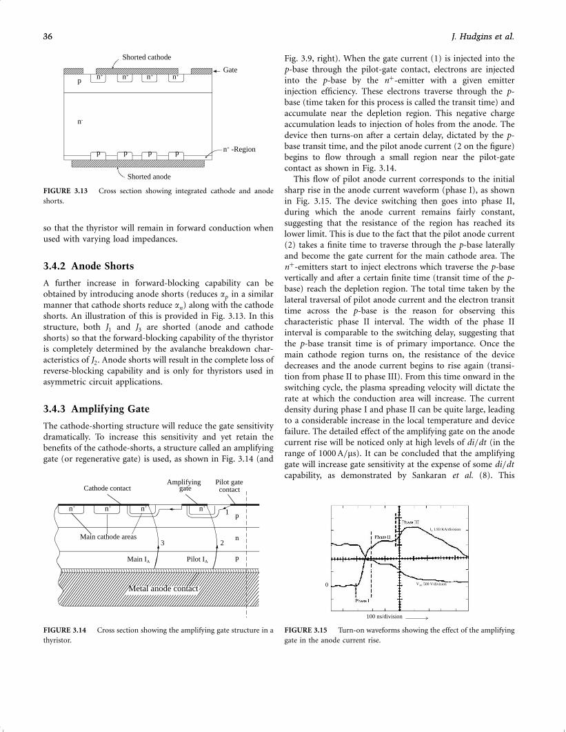
so that the thyristor will remain in forward conduction when
used with varying load impedances.
3.4.2 Anode Shorts
A further increase in forward-blocking capability can be
obtained by introducing anode shorts (reduces ap in a similar
manner that cathode shorts reduce an) along with the cathode
shorts. An illustration of this is provided in Fig. 3.13. In this
structure, both J1 and J3 are shorted (anode and cathode
shorts) so that the forward-blocking capability of the thyristor
is completely determined by the avalanche breakdown char-
acteristics of J2. Anode shorts will result in the complete loss of
reverse-blocking capability and is only for thyristors used in
asymmetric circuit applications.
3.4.3 Amplifying Gate
The cathode-shorting structure will reduce the gate sensitivity
dramatically. To increase this sensitivity and yet retain the
benefits of the cathode-shorts, a structure called an amplifying
gate (or regenerative gate) is used, as shown in Fig. 3.14 (and
Fig. 3.9, right). When the gate current (1) is injected into the
p-base through the pilot-gate contact, electrons are injected
into the p-base by the nþ-emitter with a given emitter
injection efficiency. These electrons traverse through the p-
base (time taken for this process is called the transit time) and
accumulate near the depletion region. This negative charge
accumulation leads to injection of holes from the anode. The
device then turns-on after a certain delay, dictated by the p-
base transit time, and the pilot anode current (2 on the figure)
begins to flow through a small region near the pilot-gate
contact as shown in Fig. 3.14.
This flow of pilot anode current corresponds to the initial
sharp rise in the anode current waveform (phase I), as shown
in Fig. 3.15. The device switching then goes into phase II,
during which the anode current remains fairly constant,
suggesting that the resistance of the region has reached its
lower limit. This is due to the fact that the pilot anode current
(2) takes a finite time to traverse through the p-base laterally
and become the gate current for the main cathode area. The
nþ-emitters start to inject electrons which traverse the p-base
vertically and after a certain finite time (transit time of the p-
base) reach the depletion region. The total time taken by the
lateral traversal of pilot anode current and the electron transit
time across the p-base is the reason for observing this
characteristic phase II interval. The width of the phase II
interval is comparable to the switching delay, suggesting that
the p-base transit time is of primary importance. Once the
main cathode region turns on, the resistance of the device
decreases and the anode current begins to rise again (transi-
tion from phase II to phase III). From this time onward in the
switching cycle, the plasma spreading velocity will dictate the
rate at which the conduction area will increase. The current
density during phase I and phase II can be quite large, leading
to a considerable increase in the local temperature and device
failure. The detailed effect of the amplifying gate on the anode
current rise will be noticed only at high levels of di=dt (in the
range of 1000 A=ms). It can be concluded that the amplifying
gate will increase gate sensitivity at the expense of some di=dt
capability, as demonstrated by Sankaran et al. (8). This
pn+ n+ n+ n+
n-
p p p p
Gate
n+ -Region
Shorted anode
Shorted cathode
FIGURE 3.13 Cross section showing integrated cathode and anode
shorts.
Metal anode contact
n+ n+ n+ n+
Main cathode areas
Cathode contactAmplifying
gatePilot gatecontact
Main IA Pilot IA
p
n
p
3 2
1
FIGURE 3.14 Cross section showing the amplifying gate structure in a
thyristor.
0
100 ns/division
IA 1.93 KA/division
VAK 500 V/division
FIGURE 3.15 Turn-on waveforms showing the effect of the amplifying
gate in the anode current rise.
36 J. Hudgins et al.36 J. Hudgins et al.
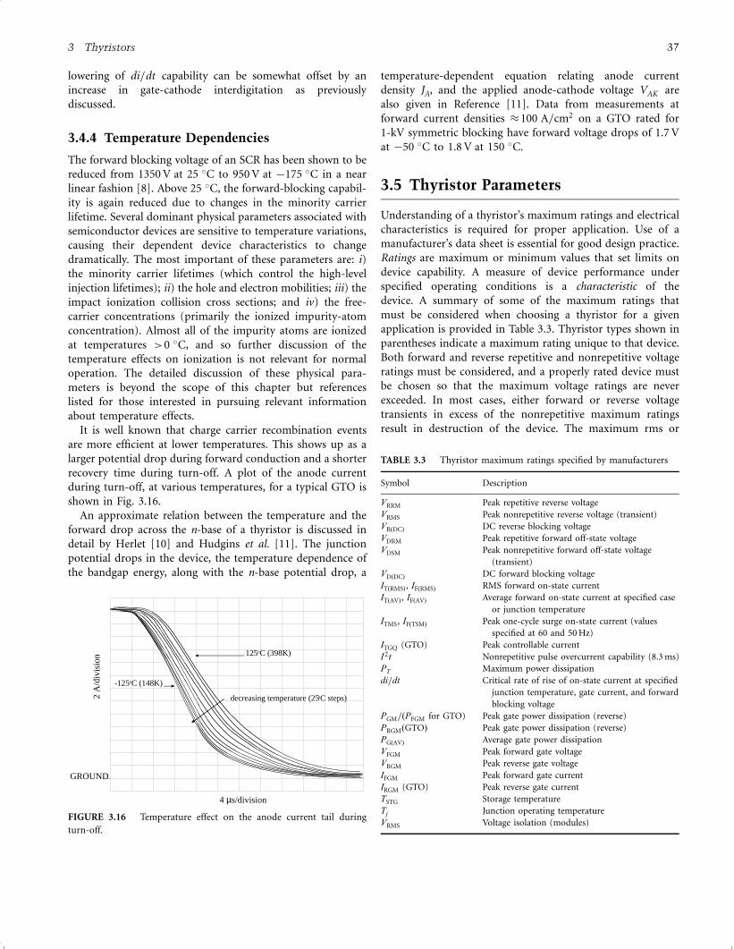
lowering of di=dt capability can be somewhat offset by an
increase in gate-cathode interdigitation as previously
discussed.
3.4.4 Temperature Dependencies
The forward blocking voltage of an SCR has been shown to be
reduced from 1350 V at 25 �C to 950 V at ÿ175 �C in a near
linear fashion [8]. Above 25 �C, the forward-blocking capabil-
ity is again reduced due to changes in the minority carrier
lifetime. Several dominant physical parameters associated with
semiconductor devices are sensitive to temperature variations,
causing their dependent device characteristics to change
dramatically. The most important of these parameters are: i)
the minority carrier lifetimes (which control the high-level
injection lifetimes); ii) the hole and electron mobilities; iii) the
impact ionization collision cross sections; and iv) the free-
carrier concentrations (primarily the ionized impurity-atom
concentration). Almost all of the impurity atoms are ionized
at temperatures >0 �C, and so further discussion of the
temperature effects on ionization is not relevant for normal
operation. The detailed discussion of these physical para-
meters is beyond the scope of this chapter but references
listed for those interested in pursuing relevant information
about temperature effects.
It is well known that charge carrier recombination events
are more efficient at lower temperatures. This shows up as a
larger potential drop during forward conduction and a shorter
recovery time during turn-off. A plot of the anode current
during turn-off, at various temperatures, for a typical GTO is
shown in Fig. 3.16.
An approximate relation between the temperature and the
forward drop across the n-base of a thyristor is discussed in
detail by Herlet [10] and Hudgins et al. [11]. The junction
potential drops in the device, the temperature dependence of
the bandgap energy, along with the n-base potential drop, a
temperature-dependent equation relating anode current
density JA, and the applied anode-cathode voltage VAK are
also given in Reference [11]. Data from measurements at
forward current densities �100 A=cm2 on a GTO rated for
1-kV symmetric blocking have forward voltage drops of 1.7 V
at ÿ50 �C to 1.8 V at 150 �C.
3.5 Thyristor Parameters
Understanding of a thyristor’s maximum ratings and electrical
characteristics is required for proper application. Use of a
manufacturer’s data sheet is essential for good design practice.
Ratings are maximum or minimum values that set limits on
device capability. A measure of device performance under
specified operating conditions is a characteristic of the
device. A summary of some of the maximum ratings that
must be considered when choosing a thyristor for a given
application is provided in Table 3.3. Thyristor types shown in
parentheses indicate a maximum rating unique to that device.
Both forward and reverse repetitive and nonrepetitive voltage
ratings must be considered, and a properly rated device must
be chosen so that the maximum voltage ratings are never
exceeded. In most cases, either forward or reverse voltage
transients in excess of the nonrepetitive maximum ratings
result in destruction of the device. The maximum rms or
decreasing temperature (25oC steps)
-125oC (148K)
125oC (398K)
GROUND
2A
/div
isio
n
4 µs/division
FIGURE 3.16 Temperature effect on the anode current tail during
turn-off.
TABLE 3.3 Thyristor maximum ratings specified by manufacturers
Symbol Description
VRRM Peak repetitive reverse voltage
VRMS Peak nonrepetitive reverse voltage (transient)
VRðDCÞ DC reverse blocking voltage
VDRM Peak repetitive forward off-state voltage
VDSM Peak nonrepetitive forward off-state voltage
(transient)
VDðDCÞ DC forward blocking voltage
ITðRMSÞ, IFðRMSÞ RMS forward on-state current
ITðAVÞ, IFðAVÞ Average forward on-state current at specified case
or junction temperature
ITMS, IFðTSMÞ Peak one-cycle surge on-state current (values
specified at 60 and 50 Hz)
ITGQ (GTO) Peak controllable current
I2t Nonrepetitive pulse overcurrent capability (8.3 ms)
PT Maximum power dissipation
di=dt Critical rate of rise of on-state current at specified
junction temperature, gate current, and forward
blocking voltage
PGM=ðPFGM for GTO) Peak gate power dissipation (reverse)
PRGMðGTOÞ Peak gate power dissipation (reverse)
PGðAVÞ Average gate power dissipation
VFGM Peak forward gate voltage
VRGM Peak reverse gate voltage
IFGM Peak forward gate current
IRGM (GTO) Peak reverse gate current
TSTG Storage temperature
Tj Junction operating temperature
VRMS Voltage isolation (modules)
3 Thyristors 37
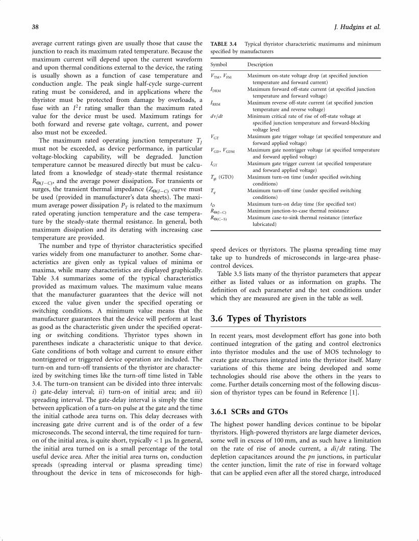
average current ratings given are usually those that cause the
junction to reach its maximum rated temperature. Because the
maximum current will depend upon the current waveform
and upon thermal conditions external to the device, the rating
is usually shown as a function of case temperature and
conduction angle. The peak single half-cycle surge-current
rating must be considered, and in applications where the
thyristor must be protected from damage by overloads, a
fuse with an I2t rating smaller than the maximum rated
value for the device must be used. Maximum ratings for
both forward and reverse gate voltage, current, and power
also must not be exceeded.
The maximum rated operating junction temperature TJ
must not be exceeded, as device performance, in particular
voltage-blocking capability, will be degraded. Junction
temperature cannot be measured directly but must be calcu-
lated from a knowledge of steady-state thermal resistance
RYðJÿCÞ, and the average power dissipation. For transients or
surges, the transient thermal impedance ðZYðJÿCÞ curve must
be used (provided in manufacturer’s data sheets). The maxi-
mum average power dissipation PT is related to the maximum
rated operating junction temperature and the case tempera-
ture by the steady-state thermal resistance. In general, both
maximum dissipation and its derating with increasing case
temperature are provided.
The number and type of thyristor characteristics specified
varies widely from one manufacturer to another. Some char-
acteristics are given only as typical values of minima or
maxima, while many characteristics are displayed graphically.
Table 3.4 summarizes some of the typical characteristics
provided as maximum values. The maximum value means
that the manufacturer guarantees that the device will not
exceed the value given under the specified operating or
switching conditions. A minimum value means that the
manufacturer guarantees that the device will perform at least
as good as the characteristic given under the specified operat-
ing or switching conditions. Thyristor types shown in
parentheses indicate a characteristic unique to that device.
Gate conditions of both voltage and current to ensure either
nontriggered or triggered device operation are included. The
turn-on and turn-off transients of the thyristor are character-
ized by switching times like the turn-off time listed in Table
3.4. The turn-on transient can be divided into three intervals:
i) gate-delay interval; ii) turn-on of initial area; and iii)
spreading interval. The gate-delay interval is simply the time
between application of a turn-on pulse at the gate and the time
the initial cathode area turns on. This delay decreases with
increasing gate drive current and is of the order of a few
microseconds. The second interval, the time required for turn-
on of the initial area, is quite short, typically <1 ms. In general,
the initial area turned on is a small percentage of the total
useful device area. After the initial area turns on, conduction
spreads (spreading interval or plasma spreading time)
throughout the device in tens of microseconds for high-
speed devices or thyristors. The plasma spreading time may
take up to hundreds of microseconds in large-area phase-
control devices.
Table 3.5 lists many of the thyristor parameters that appear
either as listed values or as information on graphs. The
definition of each parameter and the test conditions under
which they are measured are given in the table as well.
3.6 Types of Thyristors
In recent years, most development effort has gone into both
continued integration of the gating and control electronics
into thyristor modules and the use of MOS technology to
create gate structures integrated into the thyristor itself. Many
variations of this theme are being developed and some
technologies should rise above the others in the years to
come. Further details concerning most of the following discus-
sion of thyristor types can be found in Reference [1].
3.6.1 SCRs and GTOs
The highest power handling devices continue to be bipolar
thyristors. High-powered thyristors are large diameter devices,
some well in excess of 100 mm, and as such have a limitation
on the rate of rise of anode current, a di=dt rating. The
depletion capacitances around the pn junctions, in particular
the center junction, limit the rate of rise in forward voltage
that can be applied even after all the stored charge, introduced
TABLE 3.4 Typical thyristor characteristic maximums and minimum
specified by manufacturers
Symbol Description
VTM, VFM Maximum on-state voltage drop (at specified junction
temperature and forward current)
IDRM Maximum forward off-state current (at specified junction
temperature and forward voltage)
IRRM Maximum reverse off-state current (at specified junction
temperature and reverse voltage)
dn=dt Minimum critical rate of rise of off-state voltage at
specified junction temperature and forward-blocking
voltage level
VGT Maximum gate trigger voltage (at specified temperature and
forward applied voltage)
VGD, VGDM Maximum gate nontrigger voltage (at specified temperature
and forward applied voltage)
IGT Maximum gate trigger current (at specified temperature
and forward applied voltage)
Tgt (GTO) Maximum turn-on time (under specified switching
conditions)
Tq Maximum turn-off time (under specified switching
conditions)
tD Maximum turn-on delay time (for specified test)
RYðJÿCÞ Maximum junction-to-case thermal resistance
RYðCÿSÞ Maximum case-to-sink thermal resistance (interface
lubricated)
38 J. Hudgins et al.38 J. Hudgins et al.

TABLE 3.5 Symbols and definitions of major thyristor parameters
Ry Thermal Resistance Specifies the degree of temperature rise per unit of power, measuring junction temperature from a
specified external point. Defined when junction power dissipation results in steady-state thermal flow.
RyðJÿAÞ Junction-to-ambient
thermal resistance
The steady-state thermal resistance between the junction and ambient.
RyðJÿCÞ Junction-to-case thermal
resistance
The steady-state thermal resistance between the junction and case surface.
RyðJÿSÞ Junction-to-sink thermal
resistance
The steady-state thermal resistance between the junction and the heat sink mounting surface.
RyðCÿSÞ Contact thermal
resistance
The steady-state thermal resistance between the surface of the case and the heat sink mounting surface.
Zy Transient thermal
impedance
The change of temperature difference between two specified points or regions at the end of a time
interval divided by the step function change in power dissipation at the beginning of the same interval
causing the change of temperature difference.
ZyðJÿAÞ Junction-to-ambient
transient thermal
impedance
The transient thermal impedance between the junction and ambient.
ZyðJÿCÞ Junction-to-case transient
thermal impedance
The transient thermal impedance between the junction and the case surface.
ZyðJÿSÞ Junction-to-sink
transient thermal
impedance
The transient thermal impedance between the junction and the heat sink mounting surface.
TA Ambient temperature It is the temperature of the surrounding atmosphere of a device when natural or forced-air cooling is
used, and is not influenced by heat dissipation of the device.
TS Sink temperature The temperature at a specified point on the device heat sink.
TC Case temperature The temperature at a specified point on the device case.
TJ Junction temperature The device junction temperature rating. Specifies the maximum and minimum allowable operation
temperatures.
TSTG Storage temperature Specifies the maximum and minimum allowable storage temperatures (with no electrical connections).
VRRM Peak reverse blocking
voltage
Within the rated junction temperature range, and with the gate terminal open-circuited, specifies the
repetitive peak reverse anode to cathode voltage applicable on each cycle.
VRSM Transient peak reverse
blocking voltage
Within the rated junction temperature range, and with the gate terminal open-circuited, specifies the
nonrepetitive peak reverse anode to cathode voltage applicable for a time width equivalent to < 5 ms.
VRðDCÞ SCR Only DC Reverse blocking
voltage
Within the rated junction temperature range, and with the gate terminal open-circuited, specifies the
maximum value for dc anode to cathode voltage applicable in the reverse direction.
VDRM Peak forward blocking
voltage
Within the rated junction temperature range, and with the gate terminal open-circuited (SCR), or with a
specified reverse voltage between the gate and cathode (GTO), specifies the repetitive peak off-state
anode to cathode voltage applicable on each cycle. This does not apply for transient off-state voltage
application.
VDSM Transient peak forward
blocking voltage
Within the rated junction temperature range, and with the gate terminal open-circuited (SCR), or with a
specified reverse voltage between the gate and cathode (GTO), specifies the nonrepetitive off-state
anode to cathode voltage applicable for a time width equivalent to < 5 ms. This gives the maximum
instantaneous value for nonrepetitive transient off-state voltage.
VDðDCÞ DC Forward blocking
voltage
Within the rated junction temperature range, and with the gate terminal open-circuited (SCR), or with a
specified reverse voltage between the gate and cathode (GTO), specifies the maximum value for dc
anode to cathode voltage applicable in the forward direction.
dn=dt Critical rate-of-rise of
off-state voltage
dn=dt ¼ ð0:632 VDÞ=tVD is specified off-
state voltage t is time
constant for
exponential
At the maximum rated junction temperature range, and with the gate terminal open-circuited (SCR), or
with a specified reverse voltage between the gate and cathode (GTO), this specifies the maximum rate-
of-rise of off-state voltage that will not drive the device from an off-state to an on-state when an
exponential off-state voltage of specified amplitude is applied to the device.
VTM Peak on-state voltage At specified junction temperature, and when on-state current (50 or 60 Hz, half sine wave of specified
peak amplitude) is applied to the device, indicates peak-value for the resulting voltage drop.
ITðRMSÞ RMS on-state current At specified case temperature, indicates the rms value for on-state current that can be continuously
applied to the device.
ITðAVÞ Average on-state current At specified case temperature, and with the device connected to a resistive or inductive load, indicates
the average value for forward-current (sine half wave, commercial frequency) that can be continuously
applied to the device.
ITSM Peak on-state current Within the rated junction temperature range, indicates the peak-value for non-repetitive on-state current
(sine half wave, 50 or 60 Hz). This value indicated for one cycle, or as a function of a number of
cycles.
(continued )
3 Thyristors 39

TABLE 3.5 (Continued)
I2t Current-squared time The maximum, on-state, nonrepetitive short-time thermal capacity of the device and is helpful in
selecting a fuse or providing a coordinated protection scheme of the device in the equipment. This
rating is intended specifically for operation less than one half cycle of a 180� (degree) conduction
angle sinusoidal waveform. The off-state blocking capability cannot be guaranteed at values near the
maximum I2t.
di=dt Critical rate-of-rise of
on-state current
At specified case temperature, specified off-state voltage, specified gate conditions, and at a frequency of
<60 Hz, indicates the maximum rate-of-rise of on-state current which the thyristor will withstand
when switching from an off-state to an on-state, when using recommended gate drive.
IRRM Peak reverse leakage
current
At maximum rated junction temperature, indicates the peak value for reverse-current flow when a
voltage (sine half wave, 50 or 60 Hz, and having a peak value as specified for repetitive peak reverse-
voltage rating) is applied in a reverse direction to the device.
IDRM Peak forward leakage
current
At maximum rated junction temperature, indicates the peak-value for off-state-current flow when a
voltage (sine half wave, 50 or 60 Hz, and having a peak value for repetitive off-state voltage rating) is
applied in a forward direction to the device. For a GTO, a reverse voltage between the gate and
cathode is specified.
PGM ðSCRÞ Peak gate power
dissipation Within the rated junction temperature range, indicates the peak value for maximum allowable power
dissipation over a specified time period, when the device is in forward conduction between the gate
and cathode.PGFM (GTO) Peak gate forward power
dissipation
PGðAVÞ Average gate power
dissipation
Within the rated junction temperature range, indicates the average value for maximum allowable power
dissipation when the device is forward-conducting between the gate and cathode.
PGRM GTO Only Peak gate reverse power
dissipation
Within the rated junction temperature range, indicates the peak value for maximum allowable power
dissipation in the reverse direction between the gate and cathode, over a specified time period.
PGRðAVÞ GTO only Average gate reverse
power dissipation
Within the rated junction temperature range, indicates the average value for maximum allowable power
dissipation in the reverse direction between the gate and cathode.
IGFM Peak forward gate
current
Within the rated junction temperature range, indicates the peak value for forward-current flow between
the gate and cathode.
IGRM GTO Only Peak reverse gate current Within the rated junction temperature range, indicates peak value for reverse-current that can be
conducted between the gate and cathode.
VGRM Peak reverse gate voltage Within the rated junction temperature range, indicates the peak value for reverse-voltage applied between
the gate and cathode.
VGFM Peak forward gate
voltage
Within the rated junction temperature range, indicates the peak value for forward-voltage applied
between the gate and cathode.
IGT Gate current to trigger At a junction temperature of 25 �C, and with a specified off-voltage, and a specified load resistance,
indicates the minimum gate dc current required to switch the thyristor from an off-state to an on-
state.
VGT Gate voltage to trigger At a junction temperature of 25 �C, and with a specified off-state voltage, and a specified load resistance,
indicates the minimum dc gate voltage required to switch the thyristor from an off-state to an on-
state.
VGDM SCR Only Nontriggering gate
voltage
At maximum rated junction temperature, and with a specified off-state voltage applied to the device,
indicates the maximum dc gate voltage that will not switch the device from an off-state to an on-state.
ITGO GTO Only Gate controlled turn-off
current
Under specified conditions, indicates the instantaneous value for on-current usable in gate control,
specified immediately prior to device turn-off.
ton SCR Only Turn-on time At specified junction temperature, and with a peak repetitive off-state voltage of half-rated value,
followed by device turn-on using specified gate current, and when specified on-state current of
specified di=dt flows, indicated as the time required for the applied off-state voltage to drop to 10% of
its initial value after gate current application. Delay time is the term used to define the time required
for applied voltage to drop to 90% of its initial value following gate-current application. The time
required for the voltage level to drop from 90% to 10% of its initial value is referred to as rise time.
The sum of both of these defines turn-on time.
Tq SCR Only Turn-off Time Specified at maximum rated junction temperature. Device set up to conduct on-state current, followed
by applying specified reverse anode-cathode voltage to quench on-state current, and then increasing
the anode-cathode voltage at a specified rate-of-rise as determined by circuit conditions controlling the
point where the specified off-state voltage is reached. Turn-off time defines the minimum time which
the device will hold its off-state, starting from the time on-state current reached zero until the time
forward voltage is again applied (i.e., applied anode-cathode voltage becomes positive again).
tgt GTO Only Turn-on time When applying forward-current to the gate, indicates the time required to switch the device from an off-
state to an on-state.
tqt GTO Only Turn-off time When applying reverse-current to the gate, indicates the time required to switch the device from an on-
state to an off-state.
40 J. Hudgins et al.40 J. Hudgins et al.
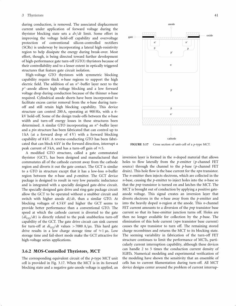
during conduction, is removed. The associated displacement
current under application of forward voltage during the
thyristor blocking state sets a dn=dt limit. Some effort in
improving the voltage hold-off capability and overvoltage
protection of conventional silicon-controlled rectifiers
(SCRs) is underway by incorporating a lateral high-resistivity
region to help dissipate the energy during break-over. Most
effort, though, is being directed toward further development
of high-performance gate turn-off (GTO) thyristors because of
their controllability and to a lesser extent in optically triggered
structures that feature gate circuit isolation.
High-voltage GTO thyristors with symmetric blocking
capability require thick n-base regions to support the high
electric field. The addition of an nþ-buffer layer next to the
pþ-anode allows high voltage blocking and a low forward
voltage drop during conduction because of the thinner n-base
required. Cylindrical anode shorts have been incorporated to
facilitate excess carrier removal from the n-base during turn-
off and still retain high blocking capability. This device
structure can control 200 A, operating at 900 Hz, with a 6-
kV hold-off. Some of the design trade-offs between the n-base
width and turn-off energy losses in these structures been
determined. A similar GTO incorporating an nþ-buffer layer
and a pin structure has been fabricated that can control up to
1 kA (at a forward drop of 4 V) with a forward blocking
capability of 8 kV. A reverse-conducting GTO has been fabri-
cated that can block 6 kV in the forward direction, interrupt a
peak current of 3 kA, and has a turn-off gain of �5.
A modified GTO structure, called a gate commutated
thyristor (GCT), has been designed and manufactured that
commutates all of the cathode current away from the cathode
region and diverts it out the gate contact. The GCT is similar
to a GTO in structure except that it has a low-loss n-buffer
region between the n-base and p-emitter. The GCT device
package is designed to result in very low parasitic inductance
and is integrated with a specially designed gate-drive circuit.
The specially designed gate drive and ring-gate package circuit
allow the GCT to be operated without a snubber circuit and
switch with higher anode di=dt , than a similar GTO. At
blocking voltages of 4.5 kV and higher the GCT seems to
provide better performance than a conventional GTO. The
speed at which the cathode current is diverted to the gate
(diGQ=dt) is directly related to the peak snubberless turn-off
capability of the GCT. The gate drive circuit can sink current
for turn-off at diGQ=dt values >7000 A=ms. This hard gate
drive results in a low charge storage time of �1 ms. Low
storage time and fail-short mode make the GCT attractive for
high-voltage series applications.
3.6.2 MOS-Controlled Thyristors, MCT
The corresponding equivalent circuit of the p-type MCT unit
cell is provided in Fig. 3.17. When the MCT is in its forward
blocking state and a negative gate-anode voltage is applied, an
inversion layer is formed in the n-doped material that allows
holes to flow laterally from the p-emitter (p-channel FET
source) through the channel to the p-base (p-channel FET
drain). This hole flow is the base current for the npn transistor.
The n-emitter then injects electrons, which are collected in the
n-base, causing the p-emitter to inject holes into the n-base so
that the pnp transistor is turned on and latches the MCT. The
MCT is brought out of conduction by applying a positive gate-
anode voltage. This signal creates an inversion layer that
diverts electrons in the n-base away from the p-emitter and
into the heavily doped n-region at the anode. This n-channel
FET current amounts to a diversion of the pnp transistor base
current so that its base-emitter junction turns off. Holes are
then no longer available for collection by the p-base. The
elimination of this hole current (npn transistor base current)
causes the npn transistor to turn off. The remaining stored
charge recombines and returns the MCT to its blocking state.
The seeming variability in fabrication of the turn-off FET
structure continues to limit the performance of MCTs, parti-
cularly current interruption capability, although these devices
can handle 2 to 5 times the conduction current density of
IGBTs. Numerical modeling and experimental verification of
the modeling have shown the sensitivity that an ensemble of
cells has to current filamentation during turn-off. All MCT
device designs center around the problem of current interrup-
anode
p
n+
n+
p+
gate
cathode
n+
pp
p-
n-
oxide
FIGURE 3.17 Cross section of unit-cell of a p-type MCT.
3 Thyristors 41
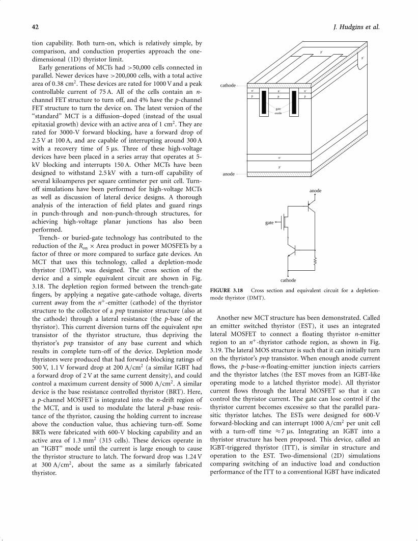
tion capability. Both turn-on, which is relatively simple, by
comparison, and conduction properties approach the one-
dimensional (1D) thyristor limit.
Early generations of MCTs had >50,000 cells connected in
parallel. Newer devices have >200,000 cells, with a total active
area of 0:38 cm2. These devices are rated for 1000 V and a peak
controllable current of 75 A. All of the cells contain an n-
channel FET structure to turn off, and 4% have the p-channel
FET structure to turn the device on. The latest version of the
‘‘standard’’ MCT is a diffusion–doped (instead of the usual
epitaxial growth) device with an active area of 1 cm2. They are
rated for 3000-V forward blocking, have a forward drop of
2.5 V at 100 A, and are capable of interrupting around 300 A
with a recovery time of 5 ms. Three of these high-voltage
devices have been placed in a series array that operates at 5-
kV blocking and interrupts 150 A. Other MCTs have been
designed to withstand 2.5 kV with a turn-off capability of
several kiloamperes per square centimeter per unit cell. Turn-
off simulations have been performed for high-voltage MCTs
as well as discussion of lateral device designs. A thorough
analysis of the interaction of field plates and guard rings
in punch-through and non-punch-through structures, for
achieving high-voltage planar junctions has also been
performed.
Trench- or buried-gate technology has contributed to the
reduction of the Ron � Area product in power MOSFETs by a
factor of three or more compared to surface gate devices. An
MCT that uses this technology, called a depletion-mode
thyristor (DMT), was designed. The cross section of the
device and a simple equivalent circuit are shown in Fig.
3.18. The depletion region formed between the trench-gate
fingers, by applying a negative gate-cathode voltage, diverts
current away from the nþ-emitter (cathode) of the thyristor
structure to the collector of a pnp transistor structure (also at
the cathode) through a lateral resistance (the p-base of the
thyristor). This current diversion turns off the equivalent npn
transistor of the thyristor structure, thus depriving the
thyristor’s pnp transistor of any base current and which
results in complete turn-off of the device. Depletion mode
thyristors were produced that had forward-blocking ratings of
500 V, 1.1 V forward drop at 200 A=cm2 (a similar IGBT had
a forward drop of 2 V at the same current density), and could
control a maximum current density of 5000 A=cm2. A similar
device is the base resistance controlled thyristor (BRT). Here,
a p-channel MOSFET is integrated into the n-drift region of
the MCT, and is used to modulate the lateral p-base resis-
tance of the thyristor, causing the holding current to increase
above the conduction value, thus achieving turn-off. Some
BRTs were fabricated with 600-V blocking capability and an
active area of 1:3 mm2 (315 cells). These devices operate in
an ‘‘IGBT’’ mode until the current is large enough to cause
the thyristor structure to latch. The forward drop was 1.24 V
at 300 A=cm2, about the same as a similarly fabricated
thyristor.
Another new MCT structure has been demonstrated. Called
an emitter switched thyristor (EST), it uses an integrated
lateral MOSFET to connect a floating thyristor n-emitter
region to an nþ-thyristor cathode region, as shown in Fig.
3.19. The lateral MOS structure is such that it can initially turn
on the thyristor’s pnp transistor. When enough anode current
flows, the p-base-n-floating-emitter junction injects carriers
and the thyristor latches (the EST moves from an IGBT-like
operating mode to a latched thyristor mode). All thyristor
current flows through the lateral MOSFET so that it can
control the thyristor current. The gate can lose control if the
thyristor current becomes excessive so that the parallel para-
sitic thyristor latches. The ESTs were designed for 600-V
forward-blocking and can interrupt 1000 A=cm2 per unit cell
with a turn-off time �7 ms. Integrating an IGBT into a
thyristor structure has been proposed. This device, called an
IGBT-triggered thyristor (ITT), is similar in structure and
operation to the EST. Two-dimensional (2D) simulations
comparing switching of an inductive load and conduction
performance of the ITT to a conventional IGBT have indicated
cathode
anode
p+
n+
n+ n+n+
p p p
gate
oxide
p+
p+
gate
anode
cathode
FIGURE 3.18 Cross section and equivalent circuit for a depletion-
mode thyristor (DMT).
42 J. Hudgins et al.42 J. Hudgins et al.
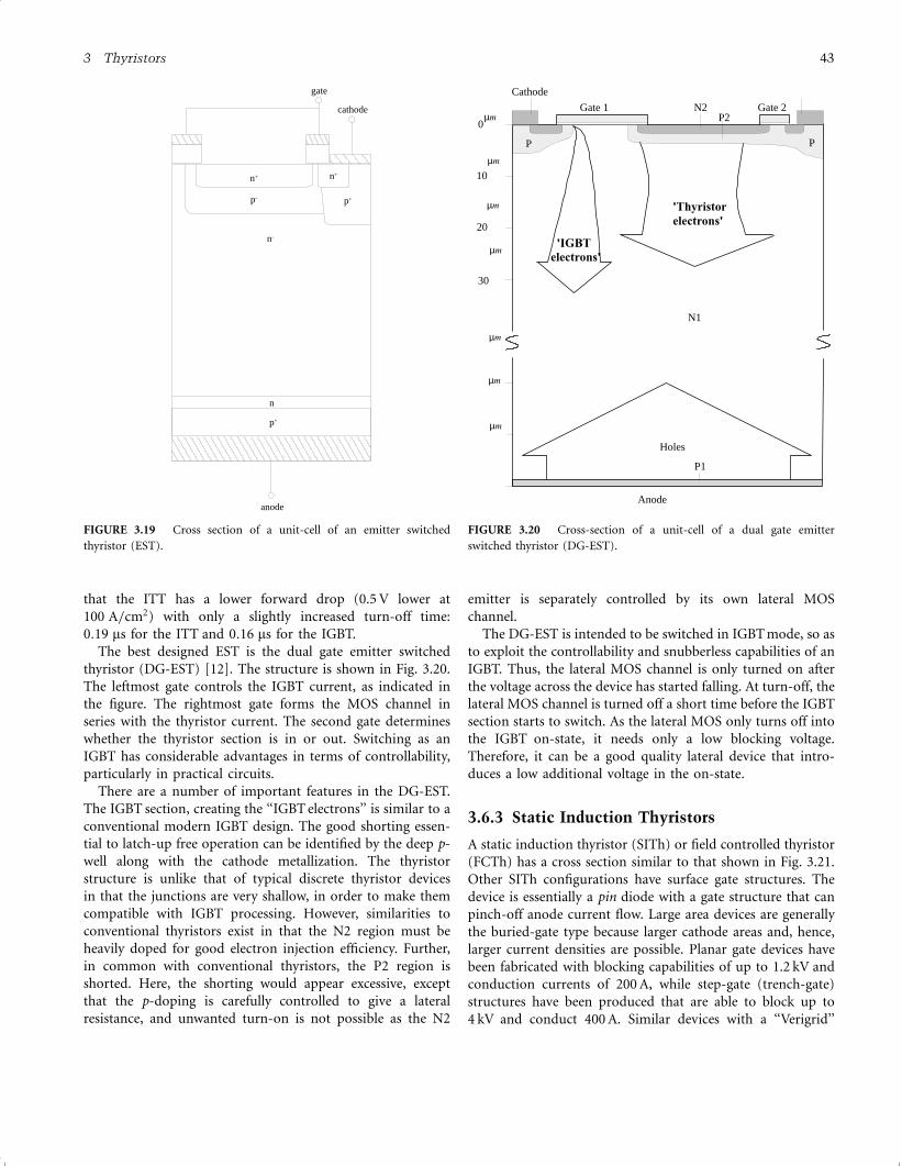
that the ITT has a lower forward drop (0.5 V lower at
100 A=cm2) with only a slightly increased turn-off time:
0:19 ms for the ITT and 0:16 ms for the IGBT.
The best designed EST is the dual gate emitter switched
thyristor (DG-EST) [12]. The structure is shown in Fig. 3.20.
The leftmost gate controls the IGBT current, as indicated in
the figure. The rightmost gate forms the MOS channel in
series with the thyristor current. The second gate determines
whether the thyristor section is in or out. Switching as an
IGBT has considerable advantages in terms of controllability,
particularly in practical circuits.
There are a number of important features in the DG-EST.
The IGBT section, creating the ‘‘IGBT electrons’’ is similar to a
conventional modern IGBT design. The good shorting essen-
tial to latch-up free operation can be identified by the deep p-
well along with the cathode metallization. The thyristor
structure is unlike that of typical discrete thyristor devices
in that the junctions are very shallow, in order to make them
compatible with IGBT processing. However, similarities to
conventional thyristors exist in that the N2 region must be
heavily doped for good electron injection efficiency. Further,
in common with conventional thyristors, the P2 region is
shorted. Here, the shorting would appear excessive, except
that the p-doping is carefully controlled to give a lateral
resistance, and unwanted turn-on is not possible as the N2
emitter is separately controlled by its own lateral MOS
channel.
The DG-EST is intended to be switched in IGBT mode, so as
to exploit the controllability and snubberless capabilities of an
IGBT. Thus, the lateral MOS channel is only turned on after
the voltage across the device has started falling. At turn-off, the
lateral MOS channel is turned off a short time before the IGBT
section starts to switch. As the lateral MOS only turns off into
the IGBT on-state, it needs only a low blocking voltage.
Therefore, it can be a good quality lateral device that intro-
duces a low additional voltage in the on-state.
3.6.3 Static Induction Thyristors
A static induction thyristor (SITh) or field controlled thyristor
(FCTh) has a cross section similar to that shown in Fig. 3.21.
Other SITh configurations have surface gate structures. The
device is essentially a pin diode with a gate structure that can
pinch-off anode current flow. Large area devices are generally
the buried-gate type because larger cathode areas and, hence,
larger current densities are possible. Planar gate devices have
been fabricated with blocking capabilities of up to 1.2 kV and
conduction currents of 200 A, while step-gate (trench-gate)
structures have been produced that are able to block up to
4 kV and conduct 400 A. Similar devices with a ‘‘Verigrid’’
anode
p+
n
n-
p-
n+ n+
p+
gate
cathode
FIGURE 3.19 Cross section of a unit-cell of an emitter switched
thyristor (EST).
'IGBTelectrons'
'Thyristorelectrons'
Cathode
Gate 1
P P
P2
P1
N2
N1
0
10
20
30
Holes
mµ
mµ
mµ
mµ
mµ
mµ
mµ
Gate 2
Anode
FIGURE 3.20 Cross-section of a unit-cell of a dual gate emitter
switched thyristor (DG-EST).
3 Thyristors 43
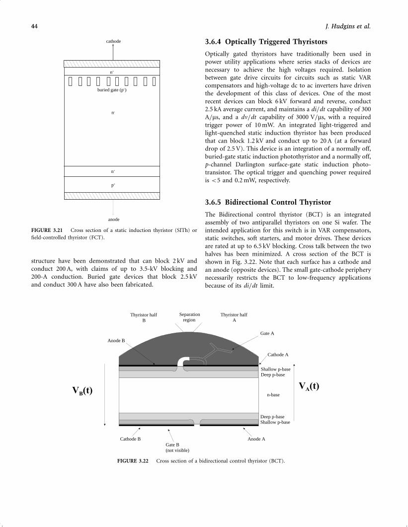
structure have been demonstrated that can block 2 kV and
conduct 200 A, with claims of up to 3.5-kV blocking and
200-A conduction. Buried gate devices that block 2.5 kV
and conduct 300 A have also been fabricated.
3.6.4 Optically Triggered Thyristors
Optically gated thyristors have traditionally been used in
power utility applications where series stacks of devices are
necessary to achieve the high voltages required. Isolation
between gate drive circuits for circuits such as static VAR
compensators and high-voltage dc to ac inverters have driven
the development of this class of devices. One of the most
recent devices can block 6 kV forward and reverse, conduct
2.5 kA average current, and maintains a di=dt capability of 300
A=ms, and a dn=dt capability of 3000 V=ms, with a required
trigger power of 10 mW. An integrated light-triggered and
light-quenched static induction thyristor has been produced
that can block 1.2 kV and conduct up to 20 A (at a forward
drop of 2.5 V). This device is an integration of a normally off,
buried-gate static induction photothyristor and a normally off,
p-channel Darlington surface-gate static induction photo-
transistor. The optical trigger and quenching power required
is <5 and 0.2 mW, respectively.
3.6.5 Bidirectional Control Thyristor
The Bidirectional control thyristor (BCT) is an integrated
assembly of two antiparallel thyristors on one Si wafer. The
intended application for this switch is in VAR compensators,
static switches, soft starters, and motor drives. These devices
are rated at up to 6.5 kV blocking. Cross talk between the two
halves has been minimized. A cross section of the BCT is
shown in Fig. 3.22. Note that each surface has a cathode and
an anode (opposite devices). The small gate-cathode periphery
necessarily restricts the BCT to low-frequency applications
because of its di=dt limit.
cathode
anode
p+
n+
n+
n-
b uried gate (p+)
FIGURE 3.21 Cross section of a static induction thyristor (SITh) or
field-controlled thyristor (FCT).
Separationregion
Thyristor half
B
Thyristor halfA
Anode B
Gate A
Cathode A
Shallow p-b aseDeep p-b ase
n-b ase
Deep p-b aseShallow p-b ase
Anode ACathode B
Gate B
(not visib le)
VB(t) VA(t)
FIGURE 3.22 Cross section of a bidirectional control thyristor (BCT).
44 J. Hudgins et al.44 J. Hudgins et al.
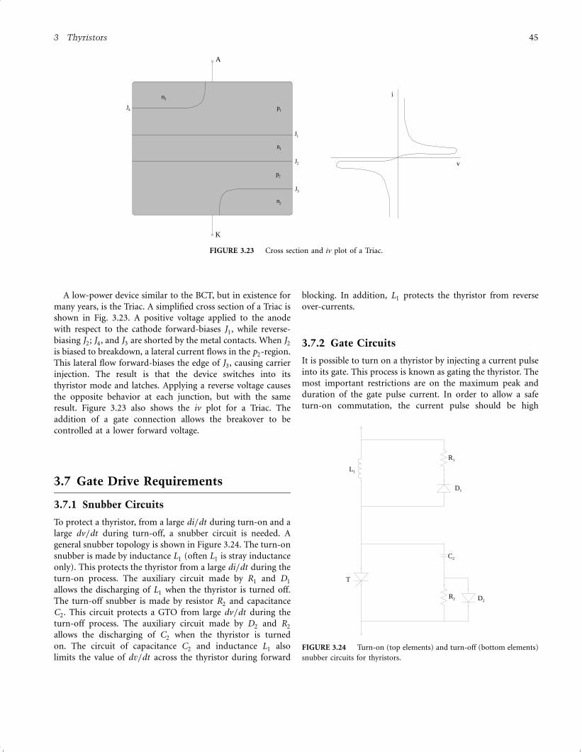
A low-power device similar to the BCT, but in existence for
many years, is the Triac. A simplified cross section of a Triac is
shown in Fig. 3.23. A positive voltage applied to the anode
with respect to the cathode forward-biases J1, while reverse-
biasing J2; J4, and J3 are shorted by the metal contacts. When J2
is biased to breakdown, a lateral current flows in the p2-region.
This lateral flow forward-biases the edge of J3, causing carrier
injection. The result is that the device switches into its
thyristor mode and latches. Applying a reverse voltage causes
the opposite behavior at each junction, but with the same
result. Figure 3.23 also shows the iv plot for a Triac. The
addition of a gate connection allows the breakover to be
controlled at a lower forward voltage.
3.7 Gate Drive Requirements
3.7.1 Snubber Circuits
To protect a thyristor, from a large di=dt during turn-on and a
large dv=dt during turn-off, a snubber circuit is needed. A
general snubber topology is shown in Figure 3.24. The turn-on
snubber is made by inductance L1 (often L1 is stray inductance
only). This protects the thyristor from a large di=dt during the
turn-on process. The auxiliary circuit made by R1 and D1
allows the discharging of L1 when the thyristor is turned off.
The turn-off snubber is made by resistor R2 and capacitance
C2. This circuit protects a GTO from large dv=dt during the
turn-off process. The auxiliary circuit made by D2 and R2
allows the discharging of C2 when the thyristor is turned
on. The circuit of capacitance C2 and inductance L1 also
limits the value of dv=dt across the thyristor during forward
blocking. In addition, L1 protects the thyristor from reverse
over-currents.
3.7.2 Gate Circuits
It is possible to turn on a thyristor by injecting a current pulse
into its gate. This process is known as gating the thyristor. The
most important restrictions are on the maximum peak and
duration of the gate pulse current. In order to allow a safe
turn-on commutation, the current pulse should be high
A
n3
J4
K
n2
n1
p2
p1
J1
J2
J3
i
v
FIGURE 3.23 Cross section and iv plot of a Triac.
L1
T
R1
D1
C2
R2 D2
FIGURE 3.24 Turn-on (top elements) and turn-off (bottom elements)
snubber circuits for thyristors.
3 Thyristors 45
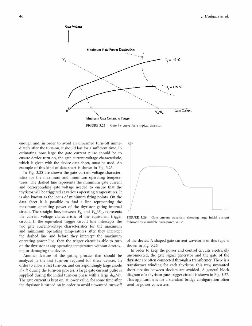
enough and, in order to avoid an unwanted turn-off imme-
diately after the turn-on, it should last for a sufficient time. In
estimating how large the gate current pulse should be to
ensure device turn on, the gate current-voltage characteristic,
which is given with the device data sheet, must be used. An
example of this kind of data sheet is shown in Fig. 3.25.
In Fig. 3.25 are shown the gate current-voltage character-
istics for the maximum and minimum operating tempera-
tures. The dashed line represents the minimum gate current
and corresponding gate voltage needed to ensure that the
thyristor will be triggered at various operating temperatures. It
is also known as the locus of minimum firing points. On the
data sheet it is possible to find a line representing the
maximum operating power of the thyristor gating internal
circuit. The straight line, between VG and VG=RG , represents
the current voltage characteristic of the equivalent trigger
circuit. If the equivalent trigger circuit line intercepts the
two gate current-voltage characteristics for the maximum
and minimum operating temperatures after they intercept
the dashed line and before they intercept the maximum
operating power line, then the trigger circuit is able to turn
on the thyristor at any operating temperature without destroy-
ing or damaging the device.
Another feature of the gating process that should be
analyzed is the fast turn-on required for these devices. In
order to allow a fast turn-on, and correspondingly large anode
di=dt during the turn-on process, a large gate current pulse is
supplied during the initial turn-on phase with a large diG=dt .
The gate current is kept on, at lower value, for some time after
the thyristor is turned on in order to avoid unwanted turn-off
of the device. A shaped gate current waveform of this type is
shown in Fig. 3.26.
In order to keep the power and control circuits electrically
unconnected, the gate signal generator and the gate of the
thyristor are often connected through a transformer. There is a
transformer winding for each thyristor; this way, unwanted
short-circuits between devices are avoided. A general block
diagram of a thyristor gate-trigger circuit is shown in Fig. 3.27.
This application is for a standard bridge configuration often
used in power converters.
FIGURE 3.25 Gate i-n curve for a typical thyristor.
0
iG(t)
t
FIGURE 3.26 Gate current waveform showing large initial current
followed by a suitable back-porch value.
46 J. Hudgins et al.46 J. Hudgins et al.
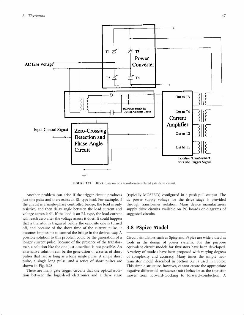
Another problem can arise if the trigger circuit produces
just one pulse and there exists an RL-type load. For example, if
the circuit is a single-phase controlled bridge, the load is only
resistive, and then delay angle between the load current and
voltage across is 0�. If the load is an RL-type, the load current
will reach zero after the voltage across it does. It could happen
that a thyristor is triggered before the opposite one is turned
off, and because of the short time of the current pulse, it
becomes impossible to control the bridge in the desired way. A
possible solution to this problem could be the generation of a
longer current pulse. Because of the presence of the transfor-
mer, a solution like the one just described is not possible. An
alternative solution can be the generation of a series of short
pulses that last as long as a long single pulse. A single short
pulse, a single long pulse, and a series of short pulses are
shown in Fig. 3.28.
There are many gate trigger circuits that use optical isola-
tion between the logic-level electronics and a drive stage
(typically MOSFETs) configured in a push-pull output. The
dc power supply voltage for the drive stage is provided
through transformer isolation. Many device manufacturers
supply drive circuits available on PC boards or diagrams of
suggested circuits.
3.8 PSpice Model
Circuit simulators such as Spice and PSpice are widely used as
tools in the design of power systems. For this purpose
equivalent circuit models for thyristors have been developed.
A variety of models have been proposed with varying degrees
of complexity and accuracy. Many times the simple two-
transistor model described in Section 3.2 is used in PSpice.
This simple structure, however, cannot create the appropriate
negative-differential-resistance (ndr) behavior as the thyristor
moves from forward-blocking to forward-conduction. A
FIGURE 3.27 Block diagram of a transformer-isolated gate drive circuit.
3 Thyristors 47
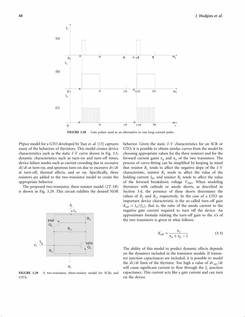
PSpice model for a GTO developed by Tsay et. al. [13] captures
many of the behaviors of thyristors. This model creates device
characteristics such as the static I-V curve shown in Fig. 3.3,
dynamic characteristics such as turn-on and turn-off times,
device failure modes such as current crowding due to excessive
di=dt at turn-on, and spurious turn-on due to excessive dn=dt
at turn-off, thermal effects, and so on. Specifically, three
resistors are added to the two-transistor model to create the
appropriate behavior.
The proposed two-transistor, three-resistor model (2T-3R)
is shown in Fig. 3.29. This circuit exhibits the desired NDR
behavior. Given the static I-V characteristics for an SCR or
GTO, it is possible to obtain similar curves from the model by
choosing appropriate values for the three resistors and for the
forward current gains ap and an of the two transistors. The
process of curve-fitting can be simplified by keeping in mind
that resistor R1 tends to affect the negative slope of the I-V
characteristic, resistor R2 tends to affect the value of the
holding current IH , and resistor R3 tends to affect the value
of the forward breakdown voltage VFBD. When modeling
thyristors with cathode or anode shorts, as described in
Section 3.4, the presence of these shorts determines the
values of R1 and R2, respectively. In the case of a GTO an
important device characteristic is the so-called turn-off gain
Koff ¼ IA=jIGj, that is, the ratio of the anode current to the
negative gate current required to turn off the device. An
approximate formula relating the turn-off gain to the a’s of
the two transistors is given in what follows:
Koff ¼an
an þ ap ÿ 1ð3:3Þ
The ability of this model to predict dynamic effects depends
on the dynamics included in the transistor models. If transis-
tor junction capacitances are included, it is possible to model
the dn=dt limit of the thyristor. Too high a value of dnAK=dt
will cause significant current to flow through the J2 junction
capacitance. This current acts like a gate current and can turn
on the device.
0
0
0
iG
iG
iG
(a)
(b )
(c)
α
α
α
α
α
α
π
π
π
π
π
π
π
π
π
2
2
2
+
+
+
π2
π2
π2
3
3
3
ω t
ω t
ωt
FIGURE 3.28 Gate pulses used as an alternative to one long current pulse.
Ki
Gi
Ai
PNPQ1i
IAi
R2i
R3i
R1i
NPNQ2i
IGi
FIGURE 3.29 A two-transistor, three-resistor model for SCRs and
GTOs.
48 J. Hudgins et al.48 J. Hudgins et al.
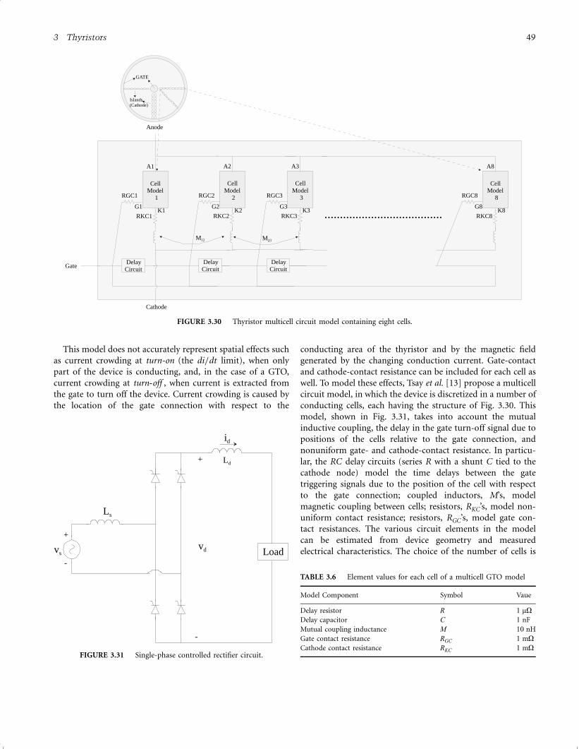
This model does not accurately represent spatial effects such
as current crowding at turn-on (the di=dt limit), when only
part of the device is conducting, and, in the case of a GTO,
current crowding at turn-off , when current is extracted from
the gate to turn off the device. Current crowding is caused by
the location of the gate connection with respect to the
conducting area of the thyristor and by the magnetic field
generated by the changing conduction current. Gate-contact
and cathode-contact resistance can be included for each cell as
well. To model these effects, Tsay et al. [13] propose a multicell
circuit model, in which the device is discretized in a number of
conducting cells, each having the structure of Fig. 3.30. This
model, shown in Fig. 3.31, takes into account the mutual
inductive coupling, the delay in the gate turn-off signal due to
positions of the cells relative to the gate connection, and
nonuniform gate- and cathode-contact resistance. In particu-
lar, the RC delay circuits (series R with a shunt C tied to the
cathode node) model the time delays between the gate
triggering signals due to the position of the cell with respect
to the gate connection; coupled inductors, M’s, model
magnetic coupling between cells; resistors, RKC’s, model non-
uniform contact resistance; resistors, RGC’s, model gate con-
tact resistances. The various circuit elements in the model
can be estimated from device geometry and measured
electrical characteristics. The choice of the number of cells is
CellModel
1
A1
RGC1
RKC1
Delay
Circuit
Cathode
Anode
Gate
K1
Cell
Model
2
A2
RGC2
RKC2
Delay
Circuit
K2G1 G2
Cell
Model
3
A3
RGC3
RKC3
Delay
Circuit
K3G3
......................................
CellModel
8
A8
RGC8
RKC8K8
G8
M12 M23
GATE
Islands
(Cathode)
FIGURE 3.30 Thyristor multicell circuit model containing eight cells.
Load
Ls
vs
+
-
+
-
Ld
id
vd
FIGURE 3.31 Single-phase controlled rectifier circuit.
TABLE 3.6 Element values for each cell of a multicell GTO model
Model Component Symbol Vaue
Delay resistor R 1 mODelay capacitor C 1 nF
Mutual coupling inductance M 10 nH
Gate contact resistance RGC 1 mOCathode contact resistance RKC 1 mO
3 Thyristors 49
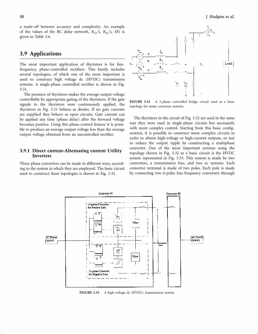
a trade-off between accuracy and complexity. An example
of the values of the RC delay network, RGC’s, RKC’s, M’s is
given in Table 3.6.
3.9 Applications
The most important application of thyristors is for line-
frequency, phase-controlled rectifiers. This family includes
several topologies, of which one of the most important is
used to construct high voltage dc (HVDC) transmission
systems. A single-phase controlled rectifier is shown in Fig.
3.31.
The presence of thyristors makes the average output voltage
controllable by appropriate gating of the thyristors. If the gate
signals to the thyristors were continuously applied, the
thyristors in Fig. 3.31 behave as diodes. If no gate currents
are supplied they behave as open circuits. Gate current can
be applied any time (phase delay) after the forward voltage
becomes positive. Using this phase-control feature it is possi-
ble to produce an average output voltage less than the average
output voltage obtained from an uncontrolled rectifier.
3.9.1 Direct current-Alternating current UtilityInverters
Three-phase converters can be made in different ways, accord-
ing to the system in which they are employed. The basic circuit
used to construct these topologies is shown in Fig. 3.32.
The thyristors in the circuit of Fig. 3.32 are used in the same
way they were used in single-phase circuits but necessarily
with more complex control. Starting from this basic config-
uration, it is possible to construct more complex circuits in
order to obtain high-voltage or high-current outputs, or just
to reduce the output ripple by constructing a multiphase
converter. One of the most important systems using the
topology shown in Fig. 3.32 as a basic circuit is the HVDC
system represented in Fig. 3.33. This system is made by two
converters, a transmission line, and two ac systems. Each
converter terminal is made of two poles. Each pole is made
by connecting two 6-pulse line-frequency converters through
FIGURE 3.32 A 3-phase controlled bridge circuit used as a basic
topology for many converter systems.
FIGURE 3.33 A high-voltage dc (HVDC) transmission system.
50 J. Hudgins et al.50 J. Hudgins et al.
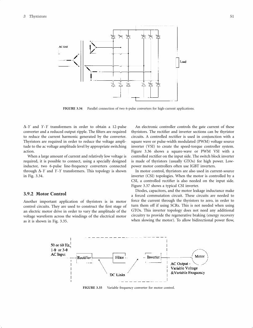
D-Y and Y -Y transformers in order to obtain a 12-pulse
converter and a reduced output ripple. The filters are required
to reduce the current harmonic generated by the converter.
Thyristors are required in order to reduce the voltage ampli-
tude to the ac voltage amplitude level by appropriate switching
action.
When a large amount of current and relatively low voltage is
required, it is possible to connect, using a specially designed
inductor, two 6-pulse line-frequency converters connected
through D-Y and Y -Y transformers. This topology is shown
in Fig. 3.34.
3.9.2 Motor Control
Another important application of thyristors is in motor
control circuits. They are used to construct the first stage of
an electric motor drive in order to vary the amplitude of the
voltage waveform across the windings of the electrical motor
as it is shown in Fig. 3.35.
An electronic controller controls the gate current of these
thyristors. The rectifier and inverter sections can be thyristor
circuits. A controlled rectifier is used in conjunction with a
square wave or pulse-width modulated (PWM) voltage source
inverter (VSI) to create the speed-torque controller system.
Figure 3.36 shows a square-wave or PWM VSI with a
controlled rectifier on the input side. The switch block inverter
is made of thyristors (usually GTOs) for high power. Low-
power motor controllers often use IGBT inverters.
In motor control, thyristors are also used in current-source
inverter (CSI) topologies. When the motor is controlled by a
CSI, a controlled rectifier is also needed on the input side.
Figure 3.37 shows a typical CSI inverter.
Diodes, capacitors, and the motor leakage inductance make
a forced commutation circuit. These circuits are needed to
force the current through the thyristors to zero, in order to
turn them off if using SCRs. This is not needed when using
GTOs. This inverter topology does not need any additional
circuitry to provide the regenerative braking (energy recovery
when slowing the motor). To allow bidirectional power flow,
FIGURE 3.34 Parallel connection of two 6-pulse converters for high-current applications.
FIGURE 3.35 Variable frequency converter for motor control.
3 Thyristors 51
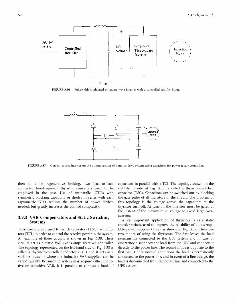
then to allow regenerative braking, two back-to-back
connected line-frequency thyristor converters used to be
employed in the past. Use of antiparallel GTOs with
symmetric blocking capability or diodes in series with each
asymmetric GTO reduces the number of power devices
needed, but greatly increases the control complexity.
3.9.3 VAR Compensators and Static SwitchingSystems
Thyristors are also used to switch capacitors (TSC) or induc-
tors (TCI) in order to control the reactive power in the system.
An example of these circuits is shown in Fig. 3.38. These
circuits act as a static VAR (volts-amps reactive) controller.
The topology represented on the left-hand side of Fig. 3.38 is
called a thyristor-controlled inductor (TCI) and it acts as a
variable inductor where the inductive VAR supplied can be
varied quickly. Because the system may require either induc-
tive or capacitive VAR, it is possible to connect a bank of
capacitors in parallel with a TCI. The topology shown on the
right-hand side of Fig. 3.38 is called a thyristor-switched
capacitor (TSC). Capacitors can be switched out by blocking
the gate pulse of all thyristors in the circuit. The problem of
this topology is the voltage across the capacitors at the
thyristor turn-off. At turn-on the thyristor must be gated at
the instant of the maximum ac voltage to avoid large over-
currents.
A less important application of thyristors is as a static
transfer switch, used to improve the reliability of uninterrup-
tible power supplies (UPS) as shown in Fig. 3.39. There are
two modes of using the thyristors. The first leaves the load
permanently connected to the UPS system and in case of
emergency disconnects the load from the UPS and connects it
directly to the power line. The second mode is opposite to the
first one. Under normal conditions the load is permanently
connected to the power line, and in event of a line outage, the
load is disconnected from the power line and connected to the
UPS system.
FIGURE 3.36 Pulsewidth modulated or square-wave inverter with a controlled rectifier input.
FIGURE 3.37 Current-source inverter on the output section of a motor drive system using capacitors for power factor correction.
52 J. Hudgins et al.52 J. Hudgins et al.
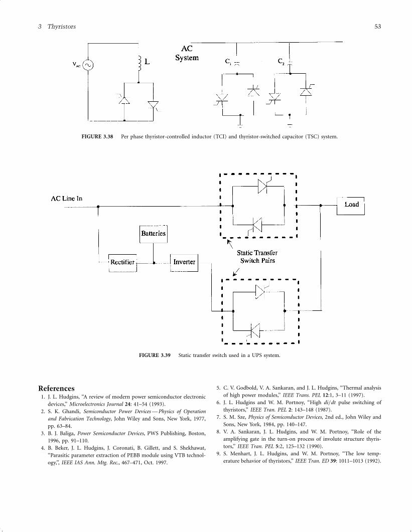
References1. J. L. Hudgins, ‘‘A review of modern power semiconductor electronic
devices,’’ Microelectronics Journal 24: 41–54 (1993).
2. S. K. Ghandi, Semiconductor Power Devices — Physics of Operation
and Fabrication Technology, John Wiley and Sons, New York, 1977,
pp. 63–84.
3. B. J. Baliga, Power Semiconductor Devices, PWS Publishing, Boston,
1996, pp. 91–110.
4. B. Beker, J. L. Hudgins, J. Coronati, B. Gillett, and S. Shekhawat,
‘‘Parasitic parameter extraction of PEBB module using VTB technol-
ogy,’’, IEEE IAS Ann. Mtg. Rec., 467–471, Oct. 1997.
5. C. V. Godbold, V. A. Sankaran, and J. L. Hudgins, ‘‘Thermal analysis
of high power modules,’’ IEEE Trans. PEL 12:1, 3–11 (1997).
6. J. L. Hudgins and W. M. Portnoy, ‘‘High di=dt pulse switching of
thyristors,’’ IEEE Tran. PEL 2: 143–148 (1987).
7. S. M. Sze, Physics of Semiconductor Devices, 2nd ed., John Wiley and
Sons, New York, 1984, pp. 140–147.
8. V. A. Sankaran, J. L. Hudgins, and W. M. Portnoy, ‘‘Role of the
amplifying gate in the turn-on process of involute structure thyris-
tors,’’ IEEE Tran. PEL 5:2, 125–132 (1990).
9. S. Menhart, J. L. Hudgins, and W. M. Portnoy, ‘‘The low temp-
erature behavior of thyristors,’’ IEEE Tran. ED 39: 1011–1013 (1992).
FIGURE 3.38 Per phase thyristor-controlled inductor (TCI) and thyristor-switched capacitor (TSC) system.
FIGURE 3.39 Static transfer switch used in a UPS system.
3 Thyristors 53

10. A. Herlet, ‘‘The forward characteristic of silicon power rectifiers
at high current densities,’’ Solid-State Electron. 11:8, 717–742 (1968).
11. J. L. Hudgins, C. V. Godbold, W. M. Portnoy, and O. M. Mueller,
‘‘Temperature effects on GTO characteristics,’’ IEEE IAS Annual Mtg.
Rec., 1182–1186, Oct. 1994.
12. P. R. Palmer and B. H. Stark, ‘‘A PSPICE model of the DG-EST based on
the ambipolar diffusion equation,’’ IEEE PESC Rec., 358–363, (1999).
13. C. L. Tsay, R. Fischl, J. Schwartzenberg, H. Kan, and J. Barrow, ‘‘A
high power circuit model for the gate turn off thyristor,’’ IEEE IAS
Annual Mtg. Rec., 390–397, Oct. 1990.
54 J. Hudgins et al.54 J. Hudgins et al.
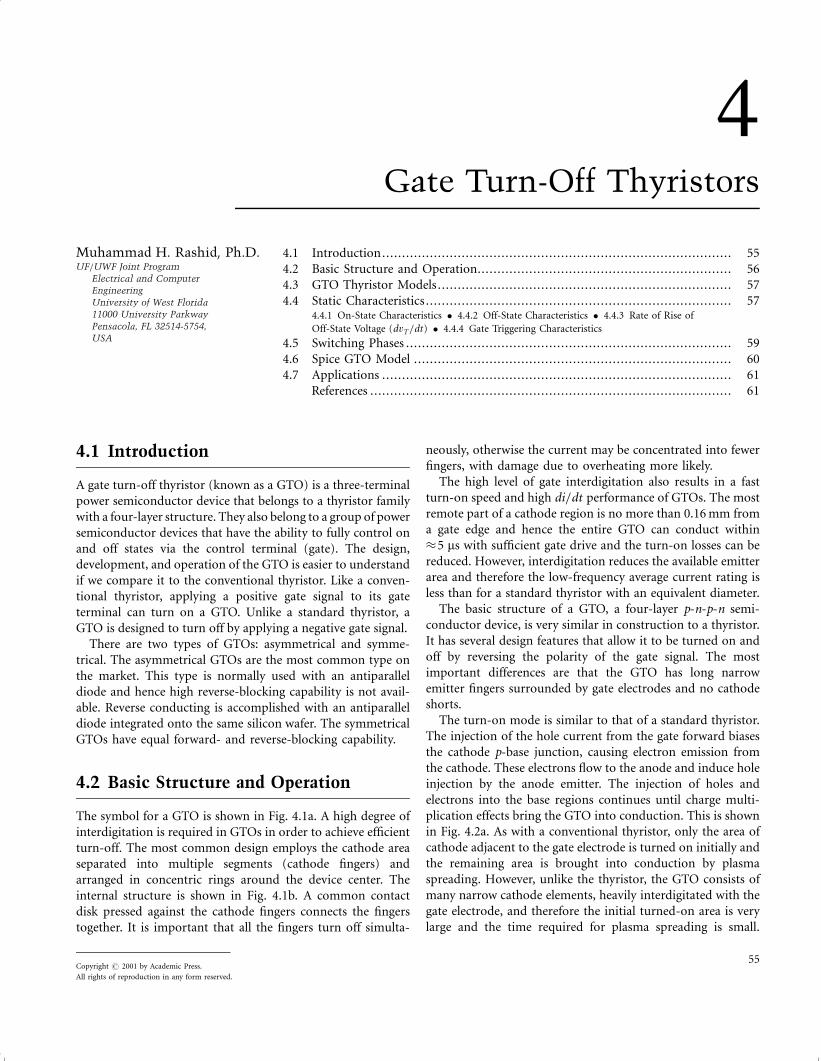
4Gate Turn-Off Thyristors
Muhammad H. Rashid, Ph.D.UF=UWF Joint Program
Electrical and Computer
Engineering
University of West Florida
11000 University Parkway
Pensacola, FL 32514-5754,
USA
4.1 Introduction
A gate turn-off thyristor (known as a GTO) is a three-terminal
power semiconductor device that belongs to a thyristor family
with a four-layer structure. They also belong to a group of power
semiconductor devices that have the ability to fully control on
and off states via the control terminal (gate). The design,
development, and operation of the GTO is easier to understand
if we compare it to the conventional thyristor. Like a conven-
tional thyristor, applying a positive gate signal to its gate
terminal can turn on a GTO. Unlike a standard thyristor, a
GTO is designed to turn off by applying a negative gate signal.
There are two types of GTOs: asymmetrical and symme-
trical. The asymmetrical GTOs are the most common type on
the market. This type is normally used with an antiparallel
diode and hence high reverse-blocking capability is not avail-
able. Reverse conducting is accomplished with an antiparallel
diode integrated onto the same silicon wafer. The symmetrical
GTOs have equal forward- and reverse-blocking capability.
4.2 Basic Structure and Operation
The symbol for a GTO is shown in Fig. 4.1a. A high degree of
interdigitation is required in GTOs in order to achieve efficient
turn-off. The most common design employs the cathode area
separated into multiple segments (cathode fingers) and
arranged in concentric rings around the device center. The
internal structure is shown in Fig. 4.1b. A common contact
disk pressed against the cathode fingers connects the fingers
together. It is important that all the fingers turn off simulta-
neously, otherwise the current may be concentrated into fewer
fingers, with damage due to overheating more likely.
The high level of gate interdigitation also results in a fast
turn-on speed and high di=dt performance of GTOs. The most
remote part of a cathode region is no more than 0.16 mm from
a gate edge and hence the entire GTO can conduct within
�5 ms with sufficient gate drive and the turn-on losses can be
reduced. However, interdigitation reduces the available emitter
area and therefore the low-frequency average current rating is
less than for a standard thyristor with an equivalent diameter.
The basic structure of a GTO, a four-layer p-n-p-n semi-
conductor device, is very similar in construction to a thyristor.
It has several design features that allow it to be turned on and
off by reversing the polarity of the gate signal. The most
important differences are that the GTO has long narrow
emitter fingers surrounded by gate electrodes and no cathode
shorts.
The turn-on mode is similar to that of a standard thyristor.
The injection of the hole current from the gate forward biases
the cathode p-base junction, causing electron emission from
the cathode. These electrons flow to the anode and induce hole
injection by the anode emitter. The injection of holes and
electrons into the base regions continues until charge multi-
plication effects bring the GTO into conduction. This is shown
in Fig. 4.2a. As with a conventional thyristor, only the area of
cathode adjacent to the gate electrode is turned on initially and
the remaining area is brought into conduction by plasma
spreading. However, unlike the thyristor, the GTO consists of
many narrow cathode elements, heavily interdigitated with the
gate electrode, and therefore the initial turned-on area is very
large and the time required for plasma spreading is small.
Copyright # 2001 by Academic Press.
All rights of reproduction in any form reserved.
55
4.1 Introduction........................................................................................ 55
4.2 Basic Structure and Operation................................................................ 56
4.3 GTO Thyristor Models .......................................................................... 57
4.4 Static Characteristics ............................................................................. 574.4.1 On-State Characteristics � 4.4.2 Off-State Characteristics � 4.4.3 Rate of Rise of
Off-State Voltage (dvT=dt) � 4.4.4 Gate Triggering Characteristics
4.5 Switching Phases .................................................................................. 59
4.6 Spice GTO Model ................................................................................ 60
4.7 Applications ........................................................................................ 61
References ........................................................................................... 61
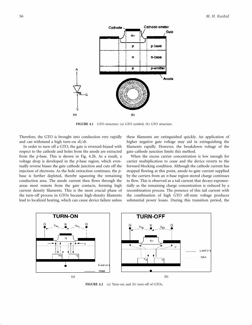
Therefore, the GTO is brought into conduction very rapidly
and can withstand a high turn-on di=dt .
In order to turn off a GTO, the gate is reversed-biased with
respect to the cathode and holes from the anode are extracted
from the p-base. This is shown in Fig. 4.2b. As a result, a
voltage drop is developed in the p-base region, which even-
tually reverse biases the gate cathode junction and cuts off the
injection of electrons. As the hole extraction continues, the p-
base is further depleted, thereby squeezing the remaining
conduction area. The anode current then flows through the
areas most remote from the gate contacts, forming high
current density filaments. This is the most crucial phase of
the turn-off process in GTOs because high-density filaments
lead to localized heating, which can cause device failure unless
these filaments are extinguished quickly. An application of
higher negative gate voltage may aid in extinguishing the
filaments rapidly. However, the breakdown voltage of the
gate-cathode junction limits this method.
When the excess carrier concentration is low enough for
carrier multiplication to cease and the device reverts to the
forward blocking condition. Although the cathode current has
stopped flowing at this point, anode-to-gate current supplied
by the carriers from an n-base region-stored charge continues
to flow. This is observed as a tail current that decays exponen-
tially as the remaining charge concentration is reduced by a
recombination process. The presence of this tail current with
the combination of high GTO off-state voltage produces
substantial power losses. During this transition period, the
FIGURE 4.1 GTO structure: (a) GTO symbol; (b) GTO structure.
(a) (b)
FIGURE 4.2 (a) Turn-on; and (b) turn-off of GTOs.
56 M. H. Rashid
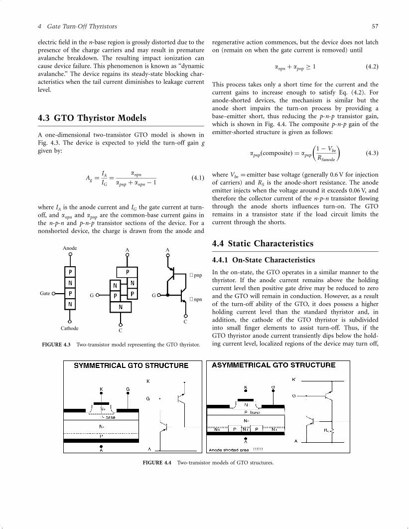
electric field in the n-base region is grossly distorted due to the
presence of the charge carriers and may result in premature
avalanche breakdown. The resulting impact ionization can
cause device failure. This phenomenon is known as ‘‘dynamic
avalanche.’’ The device regains its steady-state blocking char-
acteristics when the tail current diminishes to leakage current
level.
4.3 GTO Thyristor Models
A one-dimensional two-transistor GTO model is shown in
Fig. 4.3. The device is expected to yield the turn-off gain g
given by:
Ag ¼IA
IG
¼anpn
apnp þ anpn ÿ 1ð4:1Þ
where IA is the anode current and IG the gate current at turn-
off, and anpn and apnp are the common-base current gains in
the n-p-n and p-n-p transistor sections of the device. For a
nonshorted device, the charge is drawn from the anode and
regenerative action commences, but the device does not latch
on (remain on when the gate current is removed) until
anpn þ apnp � 1 ð4:2Þ
This process takes only a short time for the current and the
current gains to increase enough to satisfy Eq. (4.2). For
anode-shorted devices, the mechanism is similar but the
anode short impairs the turn-on process by providing a
base–emitter short, thus reducing the p-n-p transistor gain,
which is shown in Fig. 4.4. The composite p-n-p gain of the
emitter-shorted structure is given as follows:
apnpðcompositeÞ ¼ apnp
1ÿ Vbe
RSanode
� �ð4:3Þ
where Vbe ¼ emitter base voltage (generally 0.6 V for injection
of carriers) and RS is the anode-short resistance. The anode
emitter injects when the voltage around it exceeds 0.06 V, and
therefore the collector current of the n-p-n transistor flowing
through the anode shorts influences turn-on. The GTO
remains in a transistor state if the load circuit limits the
current through the shorts.
4.4 Static Characteristics
4.4.1 On-State Characteristics
In the on-state, the GTO operates in a similar manner to the
thyristor. If the anode current remains above the holding
current level then positive gate drive may be reduced to zero
and the GTO will remain in conduction. However, as a result
of the turn-off ability of the GTO, it does possess a higher
holding current level than the standard thyristor and, in
addition, the cathode of the GTO thyristor is subdivided
into small finger elements to assist turn-off. Thus, if the
GTO thyristor anode current transiently dips below the hold-
ing current level, localized regions of the device may turn off,
FIGURE 4.4 Two-transistor models of GTO structures.
Gate
Anode
Cathode
a pnp
a npn
AA
GG
C
C
FIGURE 4.3 Two-transistor model representing the GTO thyristor.
4 Gate Turn-Off Thyristors 57
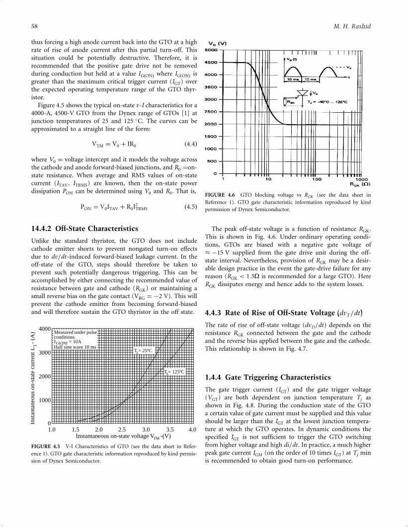
thus forcing a high anode current back into the GTO at a high
rate of rise of anode current after this partial turn-off. This
situation could be potentially destructive. Therefore, it is
recommended that the positive gate drive not be removed
during conduction but held at a value IGðONÞ where IGðONÞ is
greater than the maximum critical trigger current (IGT) over
the expected operating temperature range of the GTO thyr-
istor.
Figure 4.5 shows the typical on-state v-I characteristics for a
4000-A, 4500-V GTO from the Dynex range of GTOs [1] at
junction temperatures of 25 and 125 �C. The curves can be
approximated to a straight line of the form:
VTM ¼ V0 þ IR0 ð4:4Þ
where V0 ¼ voltage intercept and it models the voltage across
the cathode and anode forward-biased junctions, and R0 ¼on-
state resistance. When average and RMS values of on-state
current (ITAV; ITRMS) are known, then the on-state power
dissipation PON can be determined using V0 and R0. That is,
PON ¼ V0ITAV þ R0I2TRMS ð4:5Þ
14.4.2 Off-State Characteristics
Unlike the standard thyristor, the GTO does not include
cathode emitter shorts to prevent nongated turn-on effects
due to dv=dt-induced forward-biased leakage current. In the
off-state of the GTO, steps should therefore be taken to
prevent such potentially dangerous triggering. This can be
accomplished by either connecting the recommended value of
resistance between gate and cathode (RGK) or maintaining a
small reverse bias on the gate contact (VRG ¼ ÿ2 V). This will
prevent the cathode emitter from becoming forward-biased
and will therefore sustain the GTO thyristor in the off state.
The peak off-state voltage is a function of resistance RGK.
This is shown in Fig. 4.6. Under ordinary operating condi-
tions, GTOs are biased with a negative gate voltage of
� ÿ15 V supplied from the gate drive unit during the off-
state interval. Nevertheless, provision of RGK may be a desir-
able design practice in the event the gate-drive failure for any
reason (RGK < 1:5O is recommended for a large GTO). Here
RGK dissipates energy and hence adds to the system losses.
4.4.3 Rate of Rise of Off-State Voltage (dvT=dt )
The rate of rise of off-state voltage (dvD=dt) depends on the
resistance RGK connected between the gate and the cathode
and the reverse bias applied between the gate and the cathode.
This relationship is shown in Fig. 4.7.
1.4.4 Gate Triggering Characteristics
The gate trigger current (IGT) and the gate trigger voltage
(VGT) are both dependent on junction temperature Tj as
shown in Fig. 4.8. During the conduction state of the GTO
a certain value of gate current must be supplied and this value
should be larger than the IGT at the lowest junction tempera-
ture at which the GTO operates. In dynamic conditions the
specified IGT is not sufficient to trigger the GTO switching
from higher voltage and high di=dt . In practice, a much higher
peak gate current IGM (on the order of 10 times IGT) at Tj min
is recommended to obtain good turn-on performance.
4000
3000
2000
1000
01.0 1.5 2.0 2.5 3.0 3.5 4.0
Measured under pulseconditions.I
I GIONI = 10AHalf sine wave 10 ms
T = 25ºC
T = 125ºC
I
I
Instantaneous on-state voltage V -(V)
Inst
anta
neou
son-
s tate
curr
entL
-(A
)
TM
FIGURE 4.5 V-I Characteristics of GTO (see the data sheet in Refer-
ence 1). GTO gate characteristic information reproduced by kind permis-
sion of Dynex Semiconductor.
FIGURE 4.6 GTO blocking voltage vs RGK (see the data sheet in
Reference 1). GTO gate characteristic information reproduced by kind
permission of Dynex Semiconductor.
58 M. H. Rashid
4.5 Switching Phases
The switching process of a GTO thyristor goes through four
operating phases: (a) turn-on; (b) on-state; (c) turn-off; and
(d) off-state.
Turn-on: A GTO has a highly interdigited gate structure
with no regenerative gate. Thus it requires a large initial gate
trigger pulse. A typical turn-on gate pulse and its important
parameters are shown in Fig. 4.9. Minimum and maximum
values of IGM can be derived from the device data sheet. A
value of dig=dt positioned against turn-on time is given under
the device characteristics found on the data sheet [2]. The rate
of rise of gate current dig=dt will affect the device turn-on
losses. The duration of the IGM pulse should not be less than
half the minimum for time given in data sheet ratings. A
longer period will be required if the anode current di=dt is low
such that IGM is maintained until a sufficient level of anode
current is established.
On-state: Once the GTO is turned on, forward gate current
must be continued for the entire conduction period. Other-
wise, the device will not remain in conduction during the on-
state period. If large negative di=dt or anode current reversal
occurs in the circuit during the on-state, then higher values of
IG may be required. However, much lower values of IG are
required when the device has heated up.
Turn-off: The turn-off performance of a GTO is greatly
influenced by the characteristics of the gate turn-off circuit.
Thus the characteristics of the turn-off circuit must match
with the de-ice requirements. Fig. 4.10 shows the typical anode
and gate currents during the turn-off. The gate turn-off
process involves the extraction of the gate charge, the gate
avalanche period, and the anode current decay. The amount of
charge extraction is a device parameter and its value is not
affected significantly by the external circuit conditions. The
initial peak turn-off current and turn-off time, which are
important parameters of the turning-off process, depend on
the external circuit components. The device data sheet gives
typical values for IGQ.
The turn-off circuit arrangement of a GTO is shown in
Fig. 4.11. The turn-off current gain of a GTO is low, typically 6
to 15. Thus, for a GTO with a turn-off gain of 10, it will
require a turn-off gate current of 10 A to turn-off an on-state
FIGURE 4.8 GTO trigger characteristics (see the data sheet in Refer-
ence 1).
FIGURE 4.9 A typical turn-on gate pulse (see the data sheet in
Reference 2). Courtesy of Westcode.
FIGURE 4.7 dvD=dt vs RGK (see the data sheet in Reference 1). GTO
gate characteristic information reproduced by kind permission of Dynex
Semiconductor.
4 Gate Turn-Off Thyristors 59
of 100 A. A charged capacitor C is normally used to provide
the required turn-off gate current. Inductor L limits the turn-
off di=dt of the gate current through the circuit formed by
R1; R2; SW1, and L. The gate circuit supply voltage VGS
should be selected to give the required value of VGQ. The
values of R1 and R2 should also be minimized.
Off-state period: During the off-state period, which begins
after the fall of the tail current to zero, the gate should ideally
remain reverse-biased. This reverse bias ensures maximum
blocking capability and dv=dt rejection. The reverse bias can
be obtained either by keeping SW1 closed during the whole
off-state period or via a higher impedance circuit SW2 and R3
provided a minimum negative voltage exits. This higher
impedance circuit SW2 and R3 must sink the gate leakage
current.
In case of a failure of the auxiliary supplies for the gate turn-
off circuit, the gate may be in reverse-biased condition and the
GTO may not be able to block the voltage. To ensure that the
blocking voltage of the device is maintained, a minimum gate-
cathode resistance (RGK) should be applied as shown in
Fig. 4.12. The value of RGK for a given line voltage can be
derived from the data sheet.
4.6 SPICE GTO Model
A GTO may be modeled with two transistors as shown in
Fig. 4.3. However, a GTO model [3] consisting of two
thyristors, which are connected in parallel, yield improved
on-state, turn-on and turn-off characteristics. This is shown in
Fig. 4.13 with four transistors.
When the anode to cathode voltage VAK is positive and
there is no gate voltage, the GTO model will be in the off state
like a standard thyristor. If a positive voltage (VAK) is applied
to the anode with respect to the cathode and no gate pulse is
applied, IB1 ¼ IB2 ¼ 0 and, therefore, IC1 ¼ IC2 ¼ 0. Thus, no
anode current will flow and IA ¼ IK ¼ 0.
When a small voltage is applied to the gate, then IB2 is
nonzero and, therefore, both IC1 ¼ IC2 ¼ 0 are nonzero. Thus
the internal circuit will conduct and there will be a current
flow from the anode to the cathode.
When a negative gate pulse is applied to the GTO model,
the p-n-p junction near to the cathode will behave as a diode.
FIGURE 4.11 Turn-off circuit (see the data sheet in Reference 2).
Courtesy of Westcode.
FIGURE 4.12 Gate-cathode resistance, RGK (see the data sheet in
Reference 2). Courtesy of Westcode.
FIGURE 4.13 Four-transistor GTO model. Courtesy of Westcode.
FIGURE 4.10 Anode and gate currents during turn-off (see the data
sheet in Reference 2). Courtesy of Westcode.
60 M. H. Rashid

The diode will be reverse biased because the gate voltage is
negative to the cathode. Therefore, the GTO will stop conduc-
tion.
When the anode-to-cathode voltage is negative, that is, the
anode voltage is negative with respect to the cathode, the GTO
model will act like a reverse-biased diode. This is because the
p-n-p transistor will see a negative voltage at the emitter and
the n-p-n transistor will see a positive voltage at the emitter.
Therefore both transistors will be in the off state and hence the
GTO will not conduct. The SPICE subcircuit description of
the GTO model will be as follows:
4.7 Applications
Gate turn-off thyristors have many applications, including
motor drives, induction heating [4], distribution lines [5],
pulsed power [6], and flexible ac transmission systems [7].
.SUBCIRCUIT 1 2 3 ; GTO Subcircuit definition
*Terminal anode cathode gate
Q1 5 4 1 DMOD1 p-n-p ; p-n-p transistor with model DMOD1
Q3 7 6 1 DMOD1 p-n-p
Q2 4 5 2 DMOD2 n-p-n ; p-n-p transistor with model DMOD2
Q4 6 7 2 DMOD2 n-p-n
R1 7 5 10OR2 6 4 10OR3 3 7 10O.MODEL DMOD1 p-n-p ; Model statement for a p-n-p transistor
.MODEL DMOD2 n-p-n ; Model statement for an n-p-n transistor
.ENDS ; End of subcircuit definition
AcknowledgmentThe author would like to thank Mr Dinesh Chamund, Princi-
pal Engineer for Applications, Dynex Semiconductor,
Doddington Road, Lincoln LN6 3LF, United Kingdom, who
was invited to write this chapter and could not complete it due
to his work assignment
References1. Dynex Semiconductor: Data GTO data-sheets: web-site: http://
www.dynexsemi.com/products/proddata.htm
2. Westcode Semiconductor: Data GTO data-sheets: web-site: http://
www.westcode.com/ws-gto.html
3. El-Amin, I. M. A GTO PSPICE model and its applications, The Fourth
Saudi Engineering Conference, November 1995, Vol. III, pp. 271–77.
4. Busatto, G., Iannuzzo, F., and Fratelli, L. PSPICE model for GTOs,
Proceedings of Symposium on Power Electronics Electrical Drives.
Advanced Machine Power Quality. SPEEDAM Conference. Sorrento,
Italy; 3–5 June 1998, Vol. 1, pp. 2=5–10.
5. Malesani, L., and Tenti, P. Medium-frequency GTO inverter for
induction heating applications, Second European Conference on
Power Electronics and Applications: EPE. Proceedings, Grenoble,
France; 22–24 Sept. 1987, Vol. 1, pp. 271–276.
6. Souza, L. F. W., Watanabe, E. H., and Aredes, M. A. GTO controlled
series capacitor for distribution lines, International Conference on Large
High Voltage Electric Systems. CIGRE’98, 1998.
7. Chamund, D. J. Characterisation of 3.3 kV asymmetrical thyristor for
pulsed power application, IEEE Symposium Pulsed Power 2000 (Digest
No. 00=053) pp. 35=1–4, London, UK, 3–4 May 2000.
8. Moore, P. and Ashmole, P. Flexible AC transmission systems: 4.
Advanced FACTS controllers, Power Engineering Journal 12:2, 95–
100, 1998.
4 Gate Turn-Off Thyristors 61
5Power Bipolar Transistors
Marcelo GodoySimoes, Ph.D.Engineering Division
Colorado School of Mines
Golden, Colorado 80401-
1887 USA
5.1 Introduction
The first transistor was created in 1948 by a team of physicists
at the Bell Telephone Laboratories and soon became a semi-
conductor device of major importance. Before the transistor,
amplification was achieved only with vacuum tubes. Although
there are now integrated circuits with millions of transistors,
flow and control of electrical energy still require single
transistors. Therefore, power semiconductor switches consti-
tute the heart of modern power electronics. Such devices
should have larger voltage and current ratings, instant turn-
on and turn-off characteristics, very low voltage drop when
fully on, zero leakage current in blocking condition, enough
ruggedness to switch highly inductive loads, which are
measured in terms of safe operating area (SOA) and ES=b
(reverse-biased second breakdown), high-temperature and
radiation-withstand capabilities and high reliability. The
right combination of such features restricts device suitability
to only certain applications. Figure 5.1 depicts those voltage
and current ranges, in terms of frequency, at which where the
most common power semiconductors devices can operate.
The figure actually gives an overall picture of where power
semiconductors are typically applied in industries: High
voltage and current ratings permit applications in large
motor drives, induction heating, renewable energy inverters,
HVDC converters, and static VAR compensators and active
filters. By contrast, low-voltage and high-frequency applica-
tions that include switching mode power supplies, resonant
converters and motion control systems and low-frequency
with high-current and voltage devices are restricted to cyclo-
converter-fed and multimegawatt drives [1].
Power-npn or pnp bipolar transistors used to be the tradi-
tional components for driving several of these industrial
applications. However, insulated-gate bipolar-transistor
(IGBT) and metal-oxide-semiconductor field-effect transition
(MOSFET) technology have progressed so much that they are
now viable replacements for the bipolar types. Bipolar-npn or
pnp transistors still have performance areas in which they still
may be used; for example, they have lower saturation voltages
over their operating temperature range, but they are consider-
ably slower, exhibiting long turn-on and turn-off times. When
a bipolar transistor is used in a totem-pole circuit, the most
difficult design aspects to overcome are the base drive circui-
try, i.e. the required circuit for driving the base. Although
bipolar transistors have lower input capacitance than those of
MOSFETs and IGBTs, they are current driven. Thus, the drive
circuitry must generate high and prolonged input currents.
The high input impedance of the IGBT is an advantage over
its bipolar counterpart. However, input capacitance is also
high. As a result, the drive circuitry must rapidly charge and
discharge the input capacitor of the IGBT during the transi-
tion time. The IGBT low-saturation voltage performance is
analogous to bipolar power-transistor performance, even over
the operating-temperature range. The IGBT requires a
ÿ5=þ 10 V gate-emitter voltage transition to ensure reliable
output switching.
The MOSFET gate and IGBT are similar in many areas
of operation. For instance, both devices have high input
impedance, are voltage-driven, and use less silicon than the
Copyright # 2001 by Academic Press.
All rights of reproduction in any form reserved.
63
5.1 Introduction........................................................................................ 63
5.2 Basic Structure and Operation................................................................ 64
5.3 Static Characteristics ............................................................................. 65
5.4 Dynamic Switching Characteristics.......................................................... 68
5.5 Transistor Base Drive Applications .......................................................... 69
5.6 Spice Simulation of Bipolar Junction Transistors ....................................... 71
5.7 BJT Applications .................................................................................. 72
References ........................................................................................... 74
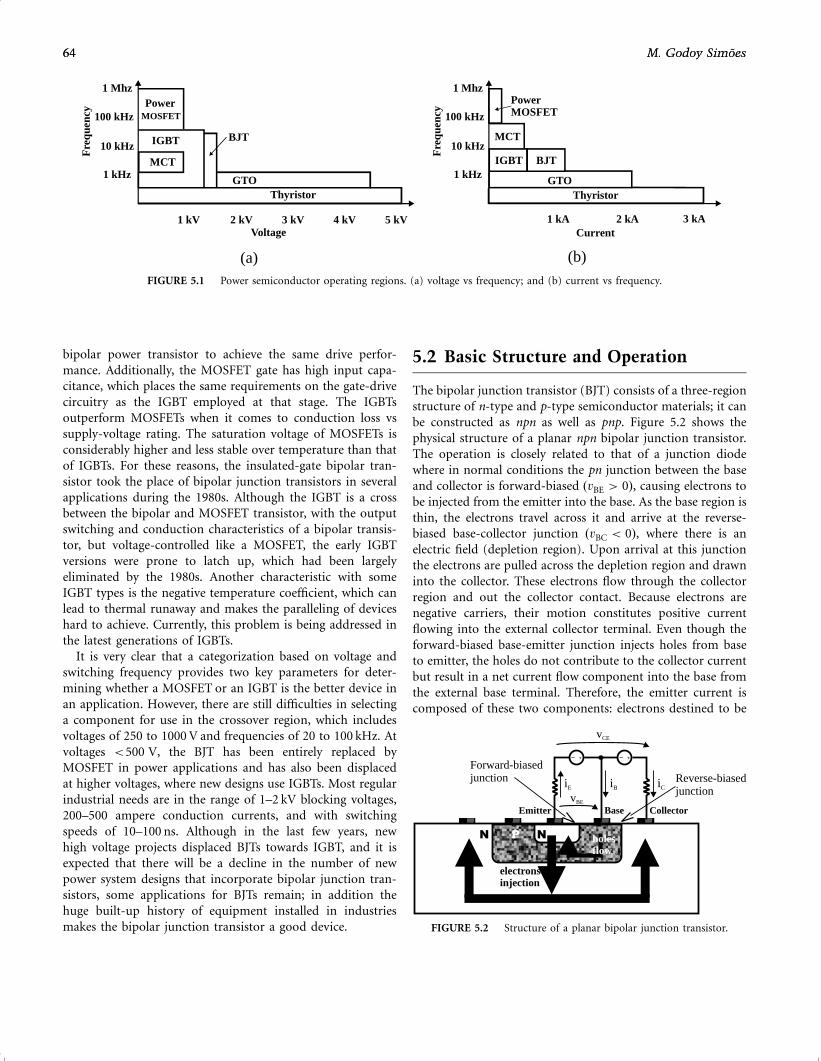
bipolar power transistor to achieve the same drive perfor-
mance. Additionally, the MOSFET gate has high input capa-
citance, which places the same requirements on the gate-drive
circuitry as the IGBT employed at that stage. The IGBTs
outperform MOSFETs when it comes to conduction loss vs
supply-voltage rating. The saturation voltage of MOSFETs is
considerably higher and less stable over temperature than that
of IGBTs. For these reasons, the insulated-gate bipolar tran-
sistor took the place of bipolar junction transistors in several
applications during the 1980s. Although the IGBT is a cross
between the bipolar and MOSFET transistor, with the output
switching and conduction characteristics of a bipolar transis-
tor, but voltage-controlled like a MOSFET, the early IGBT
versions were prone to latch up, which had been largely
eliminated by the 1980s. Another characteristic with some
IGBT types is the negative temperature coefficient, which can
lead to thermal runaway and makes the paralleling of devices
hard to achieve. Currently, this problem is being addressed in
the latest generations of IGBTs.
It is very clear that a categorization based on voltage and
switching frequency provides two key parameters for deter-
mining whether a MOSFET or an IGBT is the better device in
an application. However, there are still difficulties in selecting
a component for use in the crossover region, which includes
voltages of 250 to 1000 V and frequencies of 20 to 100 kHz. At
voltages <500 V, the BJT has been entirely replaced by
MOSFET in power applications and has also been displaced
at higher voltages, where new designs use IGBTs. Most regular
industrial needs are in the range of 1–2 kV blocking voltages,
200–500 ampere conduction currents, and with switching
speeds of 10–100 ns. Although in the last few years, new
high voltage projects displaced BJTs towards IGBT, and it is
expected that there will be a decline in the number of new
power system designs that incorporate bipolar junction tran-
sistors, some applications for BJTs remain; in addition the
huge built-up history of equipment installed in industries
makes the bipolar junction transistor a good device.
5.2 Basic Structure and Operation
The bipolar junction transistor (BJT) consists of a three-region
structure of n-type and p-type semiconductor materials; it can
be constructed as npn as well as pnp. Figure 5.2 shows the
physical structure of a planar npn bipolar junction transistor.
The operation is closely related to that of a junction diode
where in normal conditions the pn junction between the base
and collector is forward-biased ðvBE > 0Þ, causing electrons to
be injected from the emitter into the base. As the base region is
thin, the electrons travel across it and arrive at the reverse-
biased base-collector junction ðvBC < 0Þ, where there is an
electric field (depletion region). Upon arrival at this junction
the electrons are pulled across the depletion region and drawn
into the collector. These electrons flow through the collector
region and out the collector contact. Because electrons are
negative carriers, their motion constitutes positive current
flowing into the external collector terminal. Even though the
forward-biased base-emitter junction injects holes from base
to emitter, the holes do not contribute to the collector current
but result in a net current flow component into the base from
the external base terminal. Therefore, the emitter current is
composed of these two components: electrons destined to be
+_
+_
PN N holesflow
electronsinjection
vCE
vBE
iE iCiB
Reverse-biasedjunction
Forward-biasedjunction
BaseEmitter Collector
FIGURE 5.2 Structure of a planar bipolar junction transistor.
T hyristor
GT O
Power
MOSFET
MCT
BJTIGBT
1 Mhz
100 kHz
10 kHz
1 kHz
Fre
qu
en
cy
1 kV 2 kV 3 kV 4 kV 5 kV
Voltage
( a)
T hyristor
GT O
PowerMOSFET
BJT
MCT
IGBT
1 Mhz
100 kHz
10 kHz
1 kHz
Fre
qu
en
cy
1 kA 2 kA 3 kA
Current
( b)
FIGURE 5.1 Power semiconductor operating regions. (a) voltage vs frequency; and (b) current vs frequency.
64 M. Godoy Simoes64 M. Godoy Simoes
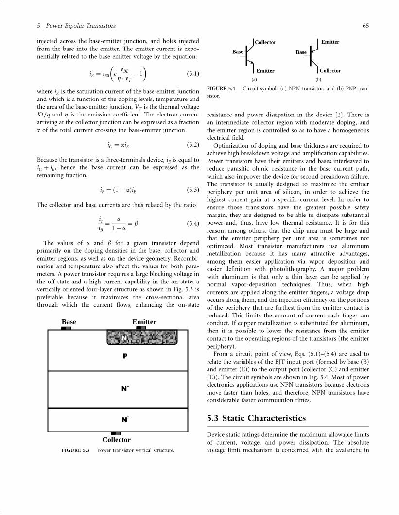
injected across the base-emitter junction, and holes injected
from the base into the emitter. The emitter current is expo-
nentially related to the base-emitter voltage by the equation:
iE ¼ iE0 enBE
Z � nT
ÿ 1
� �ð5:1Þ
where iE is the saturation current of the base-emitter junction
and which is a function of the doping levels, temperature and
the area of the base-emitter junction, VT is the thermal voltage
Kt=q and Z is the emission coefficient. The electron current
arriving at the collector junction can be expressed as a fraction
a of the total current crossing the base-emitter junction
iC ¼ aiE ð5:2Þ
Because the transistor is a three-terminals device, iE is equal to
iC þ iB , hence the base current can be expressed as the
remaining fraction,
iB ¼ ð1ÿ aÞiE ð5:3Þ
The collector and base currents are thus related by the ratio
ic
iB
¼a
1ÿ a¼ b ð5:4Þ
The values of a and b for a given transistor depend
primarily on the doping densities in the base, collector and
emitter regions, as well as on the device geometry. Recombi-
nation and temperature also affect the values for both para-
meters. A power transistor requires a large blocking voltage in
the off state and a high current capability in the on state; a
vertically oriented four-layer structure as shown in Fig. 5.3 is
preferable because it maximizes the cross-sectional area
through which the current flows, enhancing the on-state
resistance and power dissipation in the device [2]. There is
an intermediate collector region with moderate doping, and
the emitter region is controlled so as to have a homogeneous
electrical field.
Optimization of doping and base thickness are required to
achieve high breakdown voltage and amplification capabilities.
Power transistors have their emitters and bases interleaved to
reduce parasitic ohmic resistance in the base current path,
which also improves the device for second breakdown failure.
The transistor is usually designed to maximize the emitter
periphery per unit area of silicon, in order to achieve the
highest current gain at a specific current level. In order to
ensure those transistors have the greatest possible safety
margin, they are designed to be able to dissipate substantial
power and, thus, have low thermal resistance. It is for this
reason, among others, that the chip area must be large and
that the emitter periphery per unit area is sometimes not
optimized. Most transistor manufacturers use aluminum
metallization because it has many attractive advantages,
among them easier application via vapor deposition and
easier definition with photolithography. A major problem
with aluminum is that only a thin layer can be applied by
normal vapor-deposition techniques. Thus, when high
currents are applied along the emitter fingers, a voltage drop
occurs along them, and the injection efficiency on the portions
of the periphery that are farthest from the emitter contact is
reduced. This limits the amount of current each finger can
conduct. If copper metallization is substituted for aluminum,
then it is possible to lower the resistance from the emitter
contact to the operating regions of the transistors (the emitter
periphery).
From a circuit point of view, Eqs. (5.1)–(5.4) are used to
relate the variables of the BJT input port (formed by base (B)
and emitter (E)) to the output port (collector (C) and emitter
(E)). The circuit symbols are shown in Fig. 5.4. Most of power
electronics applications use NPN transistors because electrons
move faster than holes, and therefore, NPN transistors have
considerable faster commutation times.
5.3 Static Characteristics
Device static ratings determine the maximum allowable limits
of current, voltage, and power dissipation. The absolute
voltage limit mechanism is concerned with the avalanche in
P
Base Emitter
Collector
N+
N+
N-
FIGURE 5.3 Power transistor vertical structure.
Base
Emitter
Collector
( a)
Base
Emitter
Collector
( b)
FIGURE 5.4 Circuit symbols (a) NPN transistor; and (b) PNP tran-
sistor.
5 Power Bipolar Transistors 65
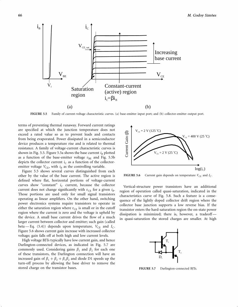
terms of preventing thermal runaway. Forward current ratings
are specified at which the junction temperature does not
exceed a rated value so as to prevent leads and contacts
from being evaporated. Power dissipated in a semiconductor
device produces a temperature rise and is related to thermal
resistance. A family of voltage-current characteristic curves is
shown in Fig. 5.5. Figure 5.5a shows the base current iB plotted
as a function of the base-emitter voltage vBE and Fig. 5.5b
depicts the collector current iC as a function of the collector-
emitter voltage VCE, with iB as the controlling variable.
Figure 5.5 shows several curves distinguished from each
other by the value of the base current. The active region is
defined where flat, horizontal portions of voltage-current
curves show ‘‘constant’’ iC current, because the collector
current does not change significantly with vCE for a given iB .
Those portions are used only for small signal transistors
operating as linear amplifiers. On the other hand, switching
power electronics systems require transistors to operate in
either the saturation region where vCE is small or in the cutoff
region where the current is zero and the voltage is upheld by
the device. A small base current drives the flow of a much
larger current between collector and emitter; such gain (called
beta — Eq. (5.4)) depends upon temperature, VCE and IC .
Figure 5.6 shows current gain increase with increased collector
voltage; gain falls off at both high and low current levels.
High voltage BJTs typically have low current gain, and hence
Darlington-connected devices, as indicated in Fig. 5.7 are
commonly used. Considering gains b1 and b2 for each one
of these transistors, the Darlington connection will have an
increased gain of b1 þ b2 þ b1b2 and diode D1 speeds up the
turn-off process by allowing the base driver to remove the
stored charge on the transistor bases.
Vertical-structure power transistors have an additional
region of operation called quasi-saturation, indicated in the
characteristics curve of Fig. 5.8. Such a feature is a conse-
quence of the lightly doped collector drift region where the
collector base junction supports a low reverse bias. If the
transistor enters the hard-saturation region the on-state power
dissipation is minimized; there is, however, a tradeoff —
in quasi-saturation the stored charges are smaller. At high
Saturationregion
Constant-current( active) region
i = iC Bβ
Increasingbase current
iC
VCE, sat
VCE
Vf
iB
VBE
( a) ( b)
FIGURE 5.5 Family of current-voltage characteristic curves. (a) base-emitter input port; and (b) collector-emitter output port.
log( )iC
Cu
rren
t G
ain
()β V = 2 V ( 125 C)CE
o
V = 2 V ( 25 C)CE
o
V = 400 V ( 25 C)CE
o
FIGURE 5.6 Current gain depends on temperature VCE and IC .
D1
T2
T1
FIGURE 5.7 Darlington-connected BJTs.
66 M. Godoy Simoes66 M. Godoy Simoes
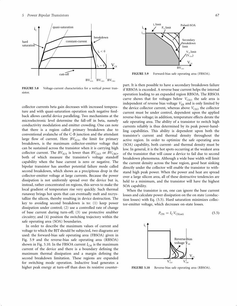
collector currents beta gain decreases with increased tempera-
ture and with quasi-saturation operation such negative feed-
back allows careful device paralleling. Two mechanisms at the
microelectronic level determine the fall-off in beta, namely
conductivity modulation and emitter crowding. One can note
that there is a region called primary breakdown due to
conventional avalanche of the C-B junction and the attendant
large flow of current. Here BVSUS, the limit for primary
breakdown, is the maximum collector-emitter voltage that
can be sustained across the transistor when it is carrying high
collector current. The BVSUS is lower than BVCEO or BVCBO,
both of which measure the transistor’s voltage standoff
capability when the base current is zero or negative. The
bipolar transistor has another potential failure mode called
second breakdown, which shows as a precipitous drop in the
collector-emitter voltage at large currents. Because the power
dissipation is not uniformly spread over the device but is,
instead, rather concentrated on regions, this serves to make the
local gradient of temperature rise very quickly. Such thermal
runaway brings hot spots that can eventually melt and recrys-
tallize the silicon, thereby resulting in device destruction. The
key to avoiding second breakdown is to: (1) keep power
dissipation under control; (2) use a controlled rate of change
of base current during turn-off; (3) use protective snubber
circuitry; and (4) position the switching trajectory within the
safe operating area (SOA) boundaries.
In order to describe the maximum values of current and
voltage to which the BJT should be subjected, two diagrams are
used: the forward-bias safe operating area (FBSOA) given in
Fig. 5.9 and the reverse-bias safe operating area (RBSOA)
shown in Fig. 5.10. In the FBSOA current ICM is the maximum
current of the device and there is a boundary defining the
maximum thermal dissipation and a margin defining the
second breakdown limitation. These regions are expanded
for switching mode operation. Inductive load generates a
higher peak energy at turn-off than does its resistive counter-
part. It is then possible to have a secondary breakdown failure
if RBSOA is exceeded. A reverse base current helps the internal
operation leading to an expanded region RBSOA. The RBSOA
curve shows that for voltages below VCEO the safe area is
independent of reverse bias voltage VEB and is only limited by
the device collector current, whereas above VCEO the collector
current must be under control, dependent upon the applied
reverse-bias voltage; in addition, temperature effects derate the
safe operating area. The ability of a transistor to switch high
currents reliably is thus determined by its peak power-hand-
ling capabilities. This ability is dependent upon both the
transistor’s current and thermal density throughout the
active region. In order to optimize the safe operating area
(SOA) capability, both current- and thermal density must be
low. In general, it is the hot spots occurring at the weakest area
of the transistor that will cause a device to fail due to second
breakdown phenomena. Although a wide base width will limit
the current density across the base region, good heat sinking
directly under the collector will enable the transistor to with-
stand high peak power. When the power and heat are spread
over a large silicon area, all of these destructive tendencies are
held to a minimum, and the transistor will have the highest
SOA capability.
When the transistor is on, one can ignore the base current
losses and calculate power dissipation on the on state (conduc-
tion losses) with Eq. (5.5). Hard saturation minimizes collec-
tor-emitter voltage, which decreases on-state losses.
PON ¼ ICVCEðsatÞ ð5:5Þ
hardsaturation
quasi-saturation
constant-current
cutt-off
BVSUS BVCBO
breakdown
i 0β =
i 0β <
BVCEO
iC
VCE
FIGURE 5.8 Voltage-current characteristics for a vertical power tran-
sistor.
VCE
BVCE0
P limittot
Secondarybreakdownlimit
i limitC
V limit
( V )CE
CEO
Pulsed-SOA
iCM
iC
FIGURE 5.9 Forward-bias safe operating area (FBSOA).
iC
VCE
VCB0VCE0
Reverse-biasvoltage VEB
FIGURE 5.10 Reverse-bias safe operating area (RBSOA).
5 Power Bipolar Transistors 67
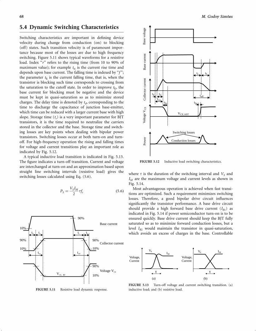
5.4 Dynamic Switching Characteristics
Switching characteristics are important in defining device
velocity during change from conduction (on) to blocking
(off) states. Such transition velocity is of paramount impor-
tance because most of the losses are due to high frequency
switching. Figure 5.11 shows typical waveforms for a resistive
load. Index ‘‘r’’ refers to the rising time (from 10 to 90% of
maximum value); for example tri is the current rise time and
depends upon base current. The falling time is indexed by ‘‘f ’’;
the parameter tfi is the current falling time, that is, when the
transistor is blocking such time corresponds to crossing from
the saturation to the cutoff state. In order to improve tfi, the
base current for blocking must be negative and the device
must be kept in quasi-saturation so as to minimize stored
charges. The delay time is denoted by td, corresponding to the
time to discharge the capacitance of junction base-emitter,
which time can be reduced with a larger current base with high
slope. Storage time (ts) is a very important parameter for BJT
transistors, it is the time required to neutralize the carriers
stored in the collector and the base. Storage time and switch-
ing losses are key points when dealing with bipolar power
transistors. Switching losses occur at both turn-on and turn-
off. For high-frequency operation the rising and falling times
for voltage and current transitions play an important role as
indicated by Fig. 5.12.
A typical inductive load transition is indicated in Fig. 5.13.
The figure indicates a turn-off transition. Current and voltage
are interchanged at turn-on and an approximation based upon
straight line switching intervals (resistive load) gives the
switching losses calculated using Eq. (5.6).
PS ¼VSIM
2tfs ð5:6Þ
where t is the duration of the switching interval and VS and
IM are the maximum voltage and current levels as shown in
Fig. 5.14.
Most advantageous operation is achieved when fast transi-
tions are optimized. Such a requirement minimizes switching
losses. Therefore, a good bipolar drive circuit influences
significantly the transistor performance. A base drive circuit
should provide a high forward base drive current (IB1) as
indicated in Fig. 5.14 if power semiconductor turn-on is to be
ensured quickly. Base drive current should keep the BJT fully
saturated so as to minimize forward conduction losses, but a
level IB2 would maintain the transistor in quasi-saturation,
which avoids an excess of charges in the base. Controllable
90%
10%VCE, SAT
Base current
Collector current
Voltage VCE
10%10%
10%
90%
90%
90%
tritd tfts
toffton
FIGURE 5.11 Resistive load dynamic response.
tfts
toff
Switching losses
Conduction losses
VCE, SA T
tritd
Co
llec
tor
curr
ent
Bas
e v
olt
age
Bas
e cu
rren
tV
olt
age
VC
EP
ow
er
tontfvtfv
FIGURE 5.12 Inductive load switching characteristics.
Voltage,Current
τ
( a)
Voltage,Current
τ
( b)
VSIM
VS IM
FIGURE 5.13 Turn-off voltage and current switching transition. (a)
inductive load; and (b) resistive load.
68 M. Godoy Simoes68 M. Godoy Simoes
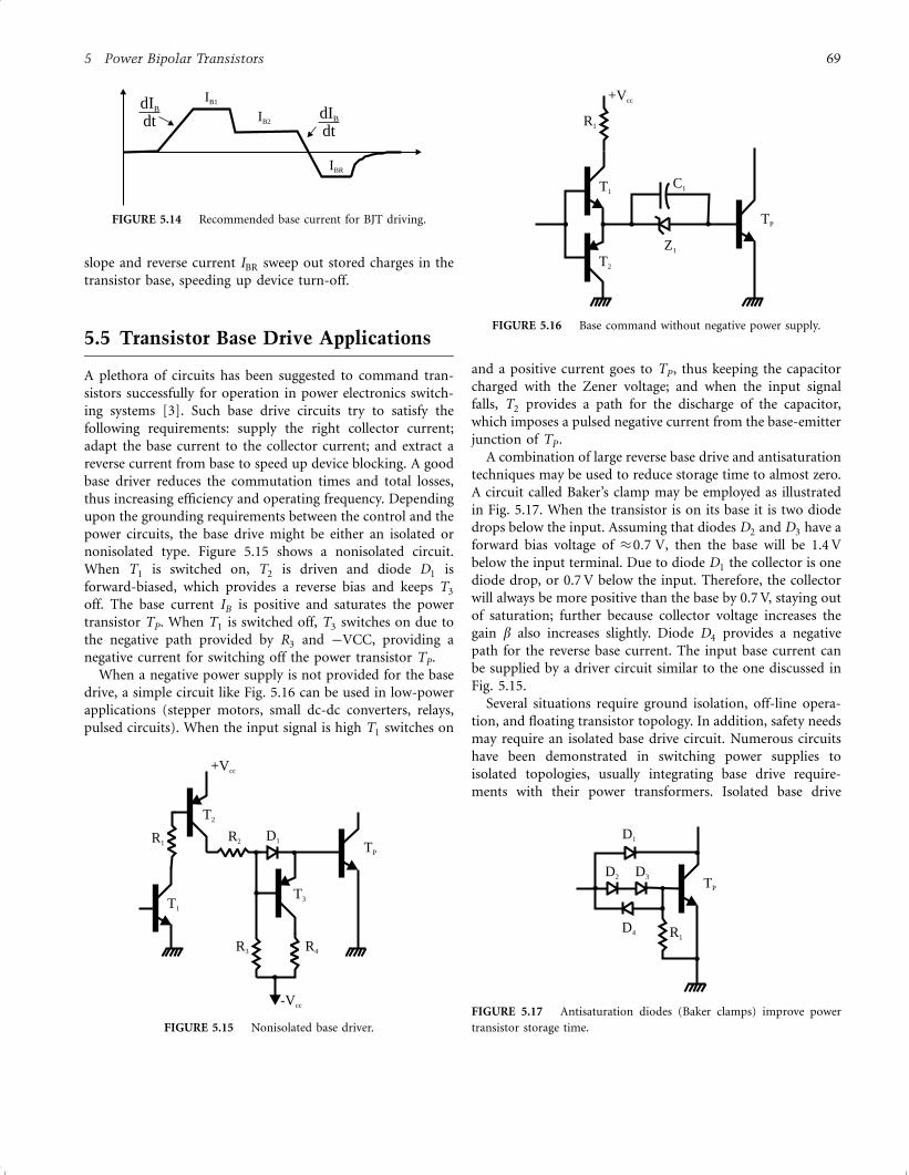
slope and reverse current IBR sweep out stored charges in the
transistor base, speeding up device turn-off.
5.5 Transistor Base Drive Applications
A plethora of circuits has been suggested to command tran-
sistors successfully for operation in power electronics switch-
ing systems [3]. Such base drive circuits try to satisfy the
following requirements: supply the right collector current;
adapt the base current to the collector current; and extract a
reverse current from base to speed up device blocking. A good
base driver reduces the commutation times and total losses,
thus increasing efficiency and operating frequency. Depending
upon the grounding requirements between the control and the
power circuits, the base drive might be either an isolated or
nonisolated type. Figure 5.15 shows a nonisolated circuit.
When T1 is switched on, T2 is driven and diode D1 is
forward-biased, which provides a reverse bias and keeps T3
off. The base current IB is positive and saturates the power
transistor TP. When T1 is switched off, T3 switches on due to
the negative path provided by R3 and ÿVCC, providing a
negative current for switching off the power transistor TP.
When a negative power supply is not provided for the base
drive, a simple circuit like Fig. 5.16 can be used in low-power
applications (stepper motors, small dc-dc converters, relays,
pulsed circuits). When the input signal is high T1 switches on
and a positive current goes to TP, thus keeping the capacitor
charged with the Zener voltage; and when the input signal
falls, T2 provides a path for the discharge of the capacitor,
which imposes a pulsed negative current from the base-emitter
junction of TP .
A combination of large reverse base drive and antisaturation
techniques may be used to reduce storage time to almost zero.
A circuit called Baker’s clamp may be employed as illustrated
in Fig. 5.17. When the transistor is on its base it is two diode
drops below the input. Assuming that diodes D2 and D3 have a
forward bias voltage of �0:7 V, then the base will be 1.4 V
below the input terminal. Due to diode D1 the collector is one
diode drop, or 0.7 V below the input. Therefore, the collector
will always be more positive than the base by 0.7 V, staying out
of saturation; further because collector voltage increases the
gain b also increases slightly. Diode D4 provides a negative
path for the reverse base current. The input base current can
be supplied by a driver circuit similar to the one discussed in
Fig. 5.15.
Several situations require ground isolation, off-line opera-
tion, and floating transistor topology. In addition, safety needs
may require an isolated base drive circuit. Numerous circuits
have been demonstrated in switching power supplies to
isolated topologies, usually integrating base drive require-
ments with their power transformers. Isolated base drive
+Vcc
T2
R1TP
T3
D1R2
R4R3
-Vcc
T1
FIGURE 5.15 Nonisolated base driver.
+Vcc
R1
TP
Z1
C1
T2
T1
FIGURE 5.16 Base command without negative power supply.
IB1
IBR
dIB
dtdIB
dt2IB
FIGURE 5.14 Recommended base current for BJT driving.
TP
R1
D2 D3
D4
D1
FIGURE 5.17 Antisaturation diodes (Baker clamps) improve power
transistor storage time.
5 Power Bipolar Transistors 69
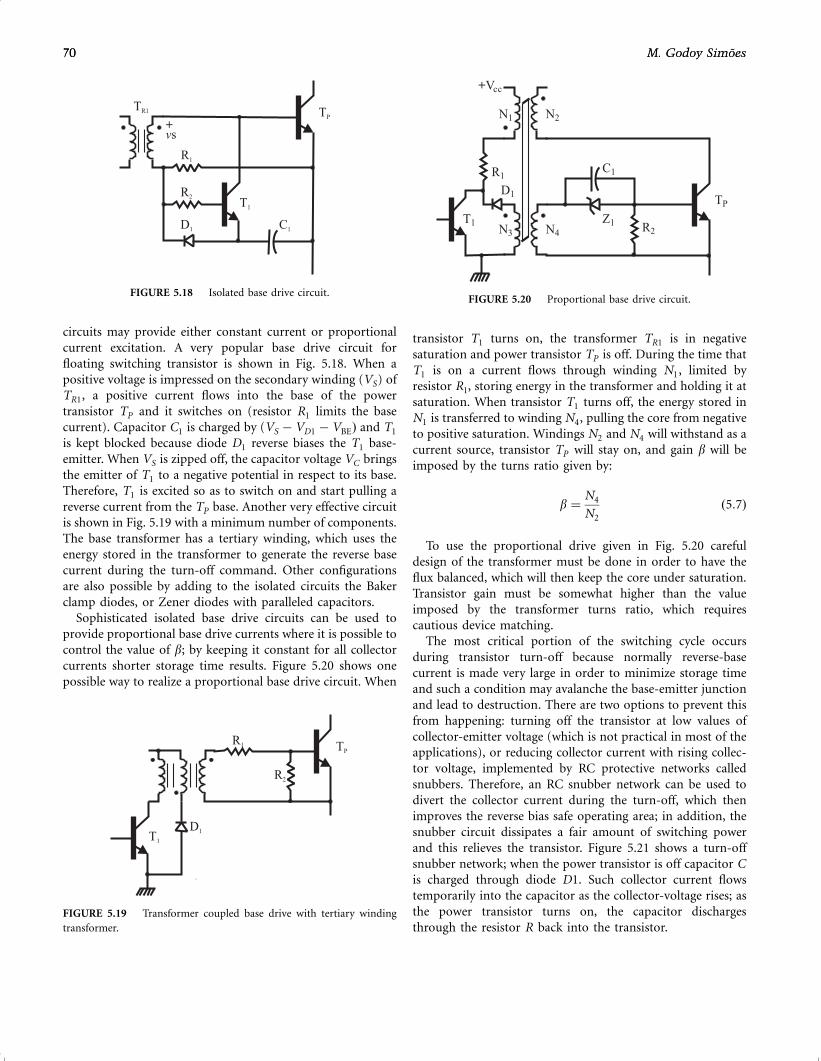
circuits may provide either constant current or proportional
current excitation. A very popular base drive circuit for
floating switching transistor is shown in Fig. 5.18. When a
positive voltage is impressed on the secondary winding (VS) of
TR1, a positive current flows into the base of the power
transistor TP and it switches on (resistor R1 limits the base
current). Capacitor C1 is charged by (VS ÿ VD1 ÿ VBEÞ and T1
is kept blocked because diode D1 reverse biases the T1 base-
emitter. When VS is zipped off, the capacitor voltage VC brings
the emitter of T1 to a negative potential in respect to its base.
Therefore, T1 is excited so as to switch on and start pulling a
reverse current from the TP base. Another very effective circuit
is shown in Fig. 5.19 with a minimum number of components.
The base transformer has a tertiary winding, which uses the
energy stored in the transformer to generate the reverse base
current during the turn-off command. Other configurations
are also possible by adding to the isolated circuits the Baker
clamp diodes, or Zener diodes with paralleled capacitors.
Sophisticated isolated base drive circuits can be used to
provide proportional base drive currents where it is possible to
control the value of b; by keeping it constant for all collector
currents shorter storage time results. Figure 5.20 shows one
possible way to realize a proportional base drive circuit. When
transistor T1 turns on, the transformer TR1 is in negative
saturation and power transistor TP is off. During the time that
T1 is on a current flows through winding N1, limited by
resistor R1, storing energy in the transformer and holding it at
saturation. When transistor T1 turns off, the energy stored in
N1 is transferred to winding N4, pulling the core from negative
to positive saturation. Windings N2 and N4 will withstand as a
current source, transistor TP will stay on, and gain b will be
imposed by the turns ratio given by:
b ¼N4
N2
ð5:7Þ
To use the proportional drive given in Fig. 5.20 careful
design of the transformer must be done in order to have the
flux balanced, which will then keep the core under saturation.
Transistor gain must be somewhat higher than the value
imposed by the transformer turns ratio, which requires
cautious device matching.
The most critical portion of the switching cycle occurs
during transistor turn-off because normally reverse-base
current is made very large in order to minimize storage time
and such a condition may avalanche the base-emitter junction
and lead to destruction. There are two options to prevent this
from happening: turning off the transistor at low values of
collector-emitter voltage (which is not practical in most of the
applications), or reducing collector current with rising collec-
tor voltage, implemented by RC protective networks called
snubbers. Therefore, an RC snubber network can be used to
divert the collector current during the turn-off, which then
improves the reverse bias safe operating area; in addition, the
snubber circuit dissipates a fair amount of switching power
and this relieves the transistor. Figure 5.21 shows a turn-off
snubber network; when the power transistor is off capacitor C
is charged through diode D1. Such collector current flows
temporarily into the capacitor as the collector-voltage rises; as
the power transistor turns on, the capacitor discharges
through the resistor R back into the transistor.
TP
R2T1
C1D1
TR1
R1
vs+
FIGURE 5.18 Isolated base drive circuit.
TP
R2
T1
R1
D1
FIGURE 5.19 Transformer coupled base drive with tertiary winding
transformer.
+Vcc
TP
R2
R1C1
T1
N1 N2
N4N3
D1
Z1
FIGURE 5.20 Proportional base drive circuit.
70 M. Godoy Simoes70 M. Godoy Simoes
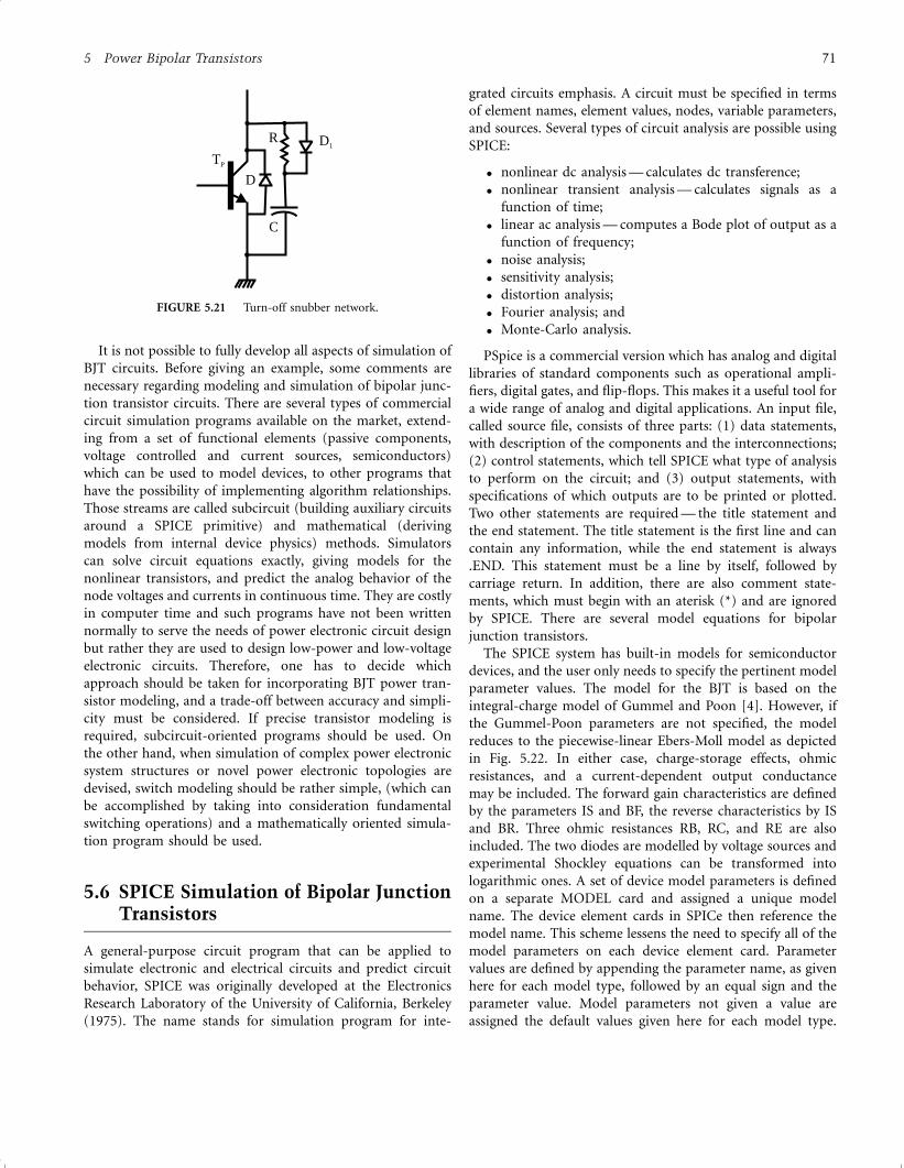
It is not possible to fully develop all aspects of simulation of
BJT circuits. Before giving an example, some comments are
necessary regarding modeling and simulation of bipolar junc-
tion transistor circuits. There are several types of commercial
circuit simulation programs available on the market, extend-
ing from a set of functional elements (passive components,
voltage controlled and current sources, semiconductors)
which can be used to model devices, to other programs that
have the possibility of implementing algorithm relationships.
Those streams are called subcircuit (building auxiliary circuits
around a SPICE primitive) and mathematical (deriving
models from internal device physics) methods. Simulators
can solve circuit equations exactly, giving models for the
nonlinear transistors, and predict the analog behavior of the
node voltages and currents in continuous time. They are costly
in computer time and such programs have not been written
normally to serve the needs of power electronic circuit design
but rather they are used to design low-power and low-voltage
electronic circuits. Therefore, one has to decide which
approach should be taken for incorporating BJT power tran-
sistor modeling, and a trade-off between accuracy and simpli-
city must be considered. If precise transistor modeling is
required, subcircuit-oriented programs should be used. On
the other hand, when simulation of complex power electronic
system structures or novel power electronic topologies are
devised, switch modeling should be rather simple, (which can
be accomplished by taking into consideration fundamental
switching operations) and a mathematically oriented simula-
tion program should be used.
5.6 SPICE Simulation of Bipolar JunctionTransistors
A general-purpose circuit program that can be applied to
simulate electronic and electrical circuits and predict circuit
behavior, SPICE was originally developed at the Electronics
Research Laboratory of the University of California, Berkeley
(1975). The name stands for simulation program for inte-
grated circuits emphasis. A circuit must be specified in terms
of element names, element values, nodes, variable parameters,
and sources. Several types of circuit analysis are possible using
SPICE:
� nonlinear dc analysis — calculates dc transference;
� nonlinear transient analysis — calculates signals as a
function of time;
� linear ac analysis — computes a Bode plot of output as a
function of frequency;
� noise analysis;
� sensitivity analysis;
� distortion analysis;
� Fourier analysis; and
� Monte-Carlo analysis.
PSpice is a commercial version which has analog and digital
libraries of standard components such as operational ampli-
fiers, digital gates, and flip-flops. This makes it a useful tool for
a wide range of analog and digital applications. An input file,
called source file, consists of three parts: (1) data statements,
with description of the components and the interconnections;
(2) control statements, which tell SPICE what type of analysis
to perform on the circuit; and (3) output statements, with
specifications of which outputs are to be printed or plotted.
Two other statements are required — the title statement and
the end statement. The title statement is the first line and can
contain any information, while the end statement is always
.END. This statement must be a line by itself, followed by
carriage return. In addition, there are also comment state-
ments, which must begin with an aterisk (*) and are ignored
by SPICE. There are several model equations for bipolar
junction transistors.
The SPICE system has built-in models for semiconductor
devices, and the user only needs to specify the pertinent model
parameter values. The model for the BJT is based on the
integral-charge model of Gummel and Poon [4]. However, if
the Gummel-Poon parameters are not specified, the model
reduces to the piecewise-linear Ebers-Moll model as depicted
in Fig. 5.22. In either case, charge-storage effects, ohmic
resistances, and a current-dependent output conductance
may be included. The forward gain characteristics are defined
by the parameters IS and BF, the reverse characteristics by IS
and BR. Three ohmic resistances RB, RC, and RE are also
included. The two diodes are modelled by voltage sources and
experimental Shockley equations can be transformed into
logarithmic ones. A set of device model parameters is defined
on a separate MODEL card and assigned a unique model
name. The device element cards in SPICe then reference the
model name. This scheme lessens the need to specify all of the
model parameters on each device element card. Parameter
values are defined by appending the parameter name, as given
here for each model type, followed by an equal sign and the
parameter value. Model parameters not given a value are
assigned the default values given here for each model type.
TP
R
C
D
D1
FIGURE 5.21 Turn-off snubber network.
5 Power Bipolar Transistors 71
As an example, the model parameters for the 2N2222A NPN
transistor are given in what follows:
.MODEL Q2N222A NPN (IS=14.34F XTI=3
EG=1.11 VAF=74.03 BF=255.9
NE=1.307 ISE=14.34F IKF=.2847 XTB=1.5
BR=6.092 NC=2 ISC=0 IKR=0
RC=1 CJC=7.306P MJC=.3416 VJC=.75 FC=.5
CJE=22.01P MJE=.377
VJE=.75 TR=46.91N TF=4.11.1P ITF=.6
VTF=1.7 XTF=3 RB=10)
Figure 5.23 shows a BJT buck chopper. The dc input voltage
is 12 V, load resistance R is 5 O, filter inductance L is 145:8 mH
and the filter capacitance C is 200 mF. The chopping frequency
is 25 kHz and the duty cycle of the chopper is 42% as indicated
by the control voltage statement ðVGÞ. The listing that follows
plots the instantaneous load current ðIOÞ, the input current
ðISÞ, the diode voltage ðVDÞ, the output voltage ðVCÞ and
calculates the Fourier coefficients of the input current ðISÞ.
This listing for the careful reader as it provides more details
and enhancements that are useful when SPICE is chosen for
simulations as shown below.
5.7 BJT Applications
Bipolar junction power transistors are applied to a variety of
power electronic functions, switching mode power supplies, dc
motor inverters, PWM inverters [5], and many other functions
too numerous to name. To conclude, three applications are
illustrated.
A flyback converter is given in Fig. 5.24. The switching
transistor is required to withstand peak collector voltage at
turn-off and peak collector currents at turn-on. In order to
limit the collector voltage to a safe value, the duty cycle must
FIGURE 5.22 Ebers-Moll transistor model.
*SOURCE
VS 1 0 DC 12V
VY 1 2 DC 0V ;Voltage source to measure input current
VG 7 3 PULSE 0V 30V 0.1NS 0/Ins 16.7US 4OUS)
*CIRCUIT
RB 7 6 250 ;Transistor base resistance
R 5 0 5
L 3 4 145.8UH
C 5 0 200UF IC=3V ;Initial voltage
VX 4 5 DC 0V ;Source to inductor current
DM 0 3 DMOD ;Freewheeling diode
.MODEL DMOD D(IS=2.22E-15 BV=1200V DJO=O TT=O)
Q1 2 6 3 3 2N6546 ;BJT switch
.MODEL 2N6546 NPN (IS=6.83E-14 BF=13 CJE=1PF CJC=607.3PF TF=26.5NS)
*ANALYSIS
.TRAN 2US 2.1MS 2MS UIC ;Transient analysis
.PROBE ;Graphics post-processor
.OPTIONS ABSTOL=1.OON RELTOL=0.01 VNTOL=0.1 ITL5=40000
.FOUR 25KHZ I(VY) ;Fourier analysis
.END
FIGURE 5.23 BJT buck chopper.
72 M. Godoy Simoes72 M. Godoy Simoes
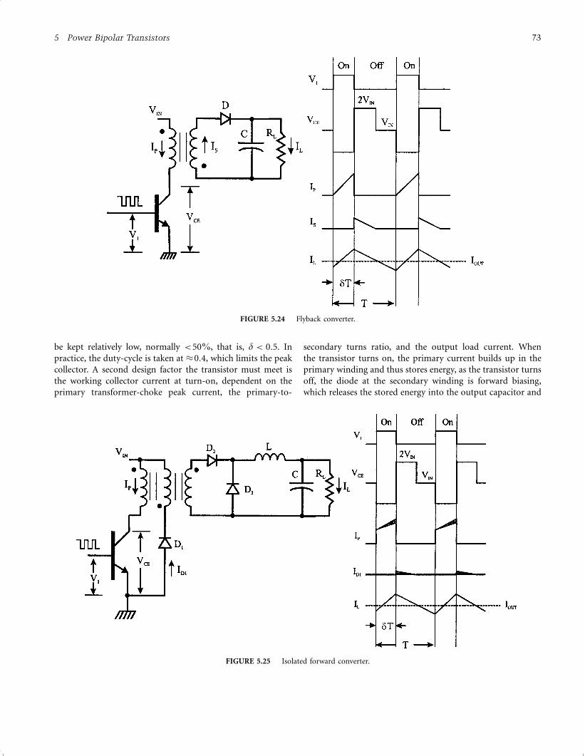
be kept relatively low, normally <50%, that is, d < 0:5. In
practice, the duty-cycle is taken at �0:4, which limits the peak
collector. A second design factor the transistor must meet is
the working collector current at turn-on, dependent on the
primary transformer-choke peak current, the primary-to-
secondary turns ratio, and the output load current. When
the transistor turns on, the primary current builds up in the
primary winding and thus stores energy, as the transistor turns
off, the diode at the secondary winding is forward biasing,
which releases the stored energy into the output capacitor and
FIGURE 5.24 Flyback converter.
FIGURE 5.25 Isolated forward converter.
5 Power Bipolar Transistors 73
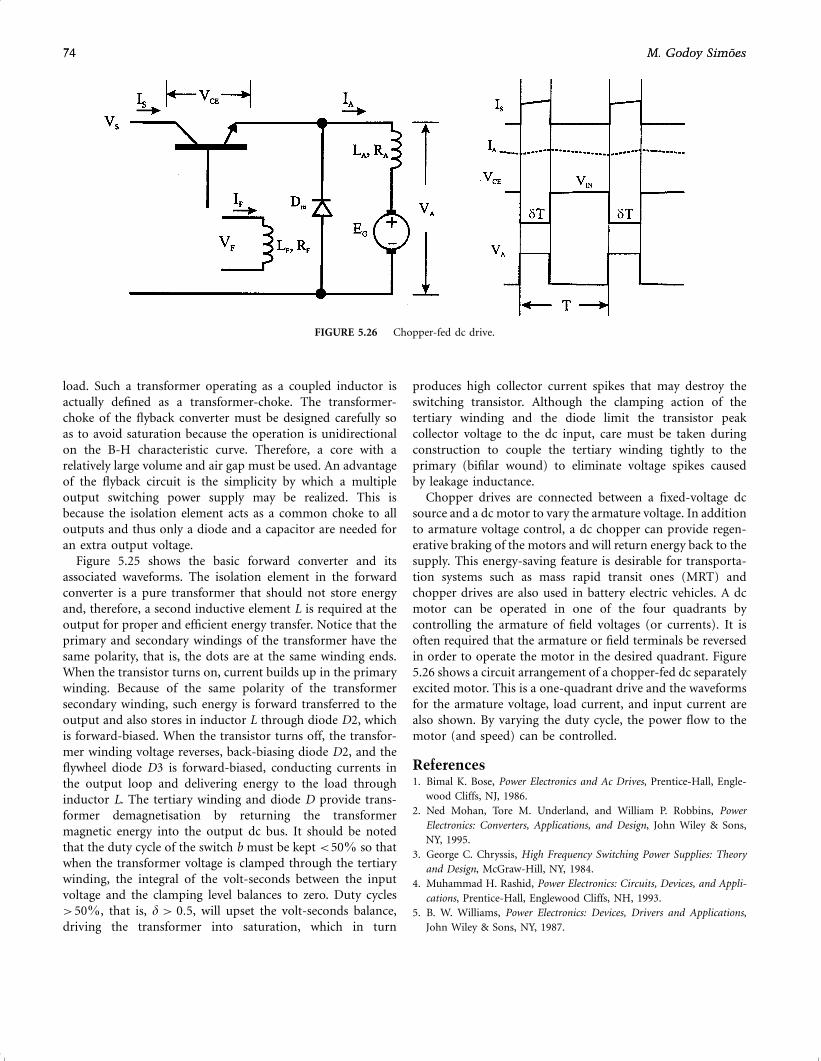
load. Such a transformer operating as a coupled inductor is
actually defined as a transformer-choke. The transformer-
choke of the flyback converter must be designed carefully so
as to avoid saturation because the operation is unidirectional
on the B-H characteristic curve. Therefore, a core with a
relatively large volume and air gap must be used. An advantage
of the flyback circuit is the simplicity by which a multiple
output switching power supply may be realized. This is
because the isolation element acts as a common choke to all
outputs and thus only a diode and a capacitor are needed for
an extra output voltage.
Figure 5.25 shows the basic forward converter and its
associated waveforms. The isolation element in the forward
converter is a pure transformer that should not store energy
and, therefore, a second inductive element L is required at the
output for proper and efficient energy transfer. Notice that the
primary and secondary windings of the transformer have the
same polarity, that is, the dots are at the same winding ends.
When the transistor turns on, current builds up in the primary
winding. Because of the same polarity of the transformer
secondary winding, such energy is forward transferred to the
output and also stores in inductor L through diode D2, which
is forward-biased. When the transistor turns off, the transfor-
mer winding voltage reverses, back-biasing diode D2, and the
flywheel diode D3 is forward-biased, conducting currents in
the output loop and delivering energy to the load through
inductor L. The tertiary winding and diode D provide trans-
former demagnetisation by returning the transformer
magnetic energy into the output dc bus. It should be noted
that the duty cycle of the switch b must be kept <50% so that
when the transformer voltage is clamped through the tertiary
winding, the integral of the volt-seconds between the input
voltage and the clamping level balances to zero. Duty cycles
>50%, that is, d > 0:5, will upset the volt-seconds balance,
driving the transformer into saturation, which in turn
produces high collector current spikes that may destroy the
switching transistor. Although the clamping action of the
tertiary winding and the diode limit the transistor peak
collector voltage to the dc input, care must be taken during
construction to couple the tertiary winding tightly to the
primary (bifilar wound) to eliminate voltage spikes caused
by leakage inductance.
Chopper drives are connected between a fixed-voltage dc
source and a dc motor to vary the armature voltage. In addition
to armature voltage control, a dc chopper can provide regen-
erative braking of the motors and will return energy back to the
supply. This energy-saving feature is desirable for transporta-
tion systems such as mass rapid transit ones (MRT) and
chopper drives are also used in battery electric vehicles. A dc
motor can be operated in one of the four quadrants by
controlling the armature of field voltages (or currents). It is
often required that the armature or field terminals be reversed
in order to operate the motor in the desired quadrant. Figure
5.26 shows a circuit arrangement of a chopper-fed dc separately
excited motor. This is a one-quadrant drive and the waveforms
for the armature voltage, load current, and input current are
also shown. By varying the duty cycle, the power flow to the
motor (and speed) can be controlled.
References1. Bimal K. Bose, Power Electronics and Ac Drives, Prentice-Hall, Engle-
wood Cliffs, NJ, 1986.
2. Ned Mohan, Tore M. Underland, and William P. Robbins, Power
Electronics: Converters, Applications, and Design, John Wiley & Sons,
NY, 1995.
3. George C. Chryssis, High Frequency Switching Power Supplies: Theory
and Design, McGraw-Hill, NY, 1984.
4. Muhammad H. Rashid, Power Electronics: Circuits, Devices, and Appli-
cations, Prentice-Hall, Englewood Cliffs, NH, 1993.
5. B. W. Williams, Power Electronics: Devices, Drivers and Applications,
John Wiley & Sons, NY, 1987.
FIGURE 5.26 Chopper-fed dc drive.
74 M. Godoy Simoes74 M. Godoy Simoes
6The Power MOSFET
Issa BatarsehCollege of Engineering and
Computer Science
University of Central Florida
Orlando, Florida 32816, USA
6.1 Introduction
This chapter gives an overview of power MOSFET semicon-
ductor switching devices. Detailed discussion of the physical
structure, fabrication and physical behavior of the device and
packaging is beyond the scope of this chapter. The emphasis
here will be on the terminal i-v switching characteristics of the
available device, turn-on and turn-off switching characteris-
tics, PSpice modeling and its current voltage and switching
limits. Even though, most of today’s available semiconductor
power devices are made of silicon or germanium materials,
other materials such as gallium arsenide, diamond and silicon
carbide are currently being tested.
One of the main contributions that led to the growth of the
power electronics field has been the unprecedented advance-
ment in semiconductor technology, especially with respect to
switching speed and power handling capabilities. The area of
power electronics started by the introduction of the silicon
controlled rectifier (SCR) in 1958. Since then, the field has
grown in parallel with the growth of the power semiconductor
device technology. In fact, the history of power electronics is
very much connected to the development of switching devices
and it emerged as a separate discipline when high-power and
MOSFET devices were introduced in the 1960s and 1970s.
Since then, the introduction of new devices has been accom-
panied by dramatic improvement in power rating and switch-
ing performance. Because of their functional importance,
drive complexity, fragility, and cost, the power electronic
design engineer must be equipped with a thorough under-
standing of the device operation, limitation, drawbacks, and
related reliability and efficiency issues.
In the 1980s, the development of power semiconductor
devices took an important turn when new process technology
was developed that allowed integration of MOS and bipolar
junction transistor (BJT) technologies on the same chip. Thus
far, two devices using this new technology have been intro-
duced: insulated bipolar transition (IGBT) and MOS-
controlled thyristor (MCT). Many integrated circuit (IC)
processing methods as well as equipment have been adapted
for the development of power devices. However, unlike micro-
electronic ICs, which process information, power device ICs
process power and so their packaging and processing techni-
ques are quite different. Power semiconductor devices repre-
sent the ‘‘heart’’ of modern power electronics, with two major
desirable characteristics of power semiconductor devices guid-
ing their development:
1. switching speed (turn-on and turn-off times); and
2. power handling capabilities (voltage blocking and
current carrying capabilities).
Improvements in both semiconductor processing technology
and manufacturing and packaging techniques have allowed
power semiconductor development for high-voltage and high
current ratings and fast turn-on and turn-off characteristics.
Copyright # 2001 by Academic Press.
All rights of reproduction in any form reserved.
75
6.1 Introduction........................................................................................ 75
6.2 The Need for Switching in Power Electronic Circuits ................................. 76
6.3 General Switching Characteristics............................................................ 786.3.1 The Ideal Switch � 6.3.2 The Practical Switch
6.4 The Power MOSFET............................................................................. 80
6.5 MOSFET Structure ............................................................................... 816.5.1 On-state Resistance � 6.5.2 Internal Body Diode � 6.5.3 Internal Capacitors
6.6 MOSFET Regions of Operation .............................................................. 836.6.1 MOSFET Switching Characteristics � 6.6.2 Turn-on Characteristics � 6.6.3 Turn-off
Characteristics � 6.6.4 Safe-Operation Area
6.7 MOSFET PSpice Model......................................................................... 936.7.1 Static Model � 6.7.2 Large Signal Model
6.8 Comparison of Switching Devices ........................................................... 96
6.9 Future Trends in Power Devices.............................................................. 98
References ........................................................................................... 99
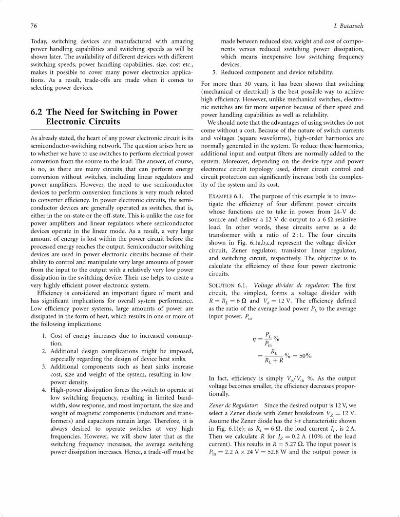
Today, switching devices are manufactured with amazing
power handling capabilities and switching speeds as will be
shown later. The availability of different devices with different
switching speeds, power handling capabilities, size, cost etc.,
makes it possible to cover many power electronics applica-
tions. As a result, trade-offs are made when it comes to
selecting power devices.
6.2 The Need for Switching in PowerElectronic Circuits
As already stated, the heart of any power electronic circuit is its
semiconductor-switching network. The question arises here as
to whether we have to use switches to perform electrical power
conversion from the source to the load. The answer, of course,
is no, as there are many circuits that can perform energy
conversion without switches, including linear regulators and
power amplifiers. However, the need to use semiconductor
devices to perform conversion functions is very much related
to converter efficiency. In power electronic circuits, the semi-
conductor devices are generally operated as switches, that is,
either in the on-state or the off-state. This is unlike the case for
power amplifiers and linear regulators where semiconductor
devices operate in the linear mode. As a result, a very large
amount of energy is lost within the power circuit before the
processed energy reaches the output. Semiconductor switching
devices are used in power electronic circuits because of their
ability to control and manipulate very large amounts of power
from the input to the output with a relatively very low power
dissipation in the switching device. Their use helps to create a
very highly efficient power electronic system.
Efficiency is considered an important figure of merit and
has significant implications for overall system performance.
Low efficiency power systems, large amounts of power are
dissipated in the form of heat, which results in one or more of
the following implications:
1. Cost of energy increases due to increased consump-
tion.
2. Additional design complications might be imposed,
especially regarding the design of device heat sinks.
3. Additional components such as heat sinks increase
cost, size and weight of the system, resulting in low-
power density.
4. High-power dissipation forces the switch to operate at
low switching frequency, resulting in limited band-
width, slow response, and most important, the size and
weight of magnetic components (inductors and trans-
formers) and capacitors remain large. Therefore, it is
always desired to operate switches at very high
frequencies. However, we will show later that as the
switching frequency increases, the average switching
power dissipation increases. Hence, a trade-off must be
made between reduced size, weight and cost of compo-
nents versus reduced switching power dissipation,
which means inexpensive low switching frequency
devices.
5. Reduced component and device reliability.
For more than 30 years, it has been shown that switching
(mechanical or electrical) is the best possible way to achieve
high efficiency. However, unlike mechanical switches, electro-
nic switches are far more superior because of their speed and
power handling capabilities as well as reliability.
We should note that the advantages of using switches do not
come without a cost. Because of the nature of switch currents
and voltages (square waveforms), high-order harmonics are
normally generated in the system. To reduce these harmonics,
additional input and output filters are normally added to the
system. Moreover, depending on the device type and power
electronic circuit topology used, driver circuit control and
circuit protection can significantly increase both the complex-
ity of the system and its cost.
EXAMPLE 6.1. The purpose of this example is to inves-
tigate the efficiency of four different power circuits
whose functions are to take in power from 24-V dc
source and deliver a 12-V dc output to a 6-O resistive
load. In other words, these circuits serve as a dc
transformer with a ratio of 2 : 1. The four circuits
shown in Fig. 6.1a,b,c,d represent the voltage divider
circuit, Zener regulator, transistor linear regulator,
and switching circuit, respectively. The objective is to
calculate the efficiency of these four power electronic
circuits.
SOLUTION 6.1. Voltage divider dc regulator: The first
circuit, the simplest, forms a voltage divider with
R ¼ RL ¼ 6 O and Vo ¼ 12 V. The efficiency defined
as the ratio of the average load power PL to the average
input power, Pin
Z ¼PL
Pin
%
¼RL
RL þ R% ¼ 50%
In fact, efficiency is simply Vo=Vin %. As the output
voltage becomes smaller, the efficiency decreases propor-
tionally.
Zener dc Regulator: Since the desired output is 12 V, we
select a Zener diode with Zener breakdown VZ ¼ 12 V.
Assume the Zener diode has the i-v characteristic shown
in Fig. 6.1(e); as RL ¼ 6 O, the load current IL, is 2 A.
Then we calculate R for IZ ¼ 0:2 A (10% of the load
current). This results in R ¼ 5:27 O. The input power is
Pin ¼ 2:2 A� 24 V ¼ 52:8 W and the output power is
76 I. Batarseh
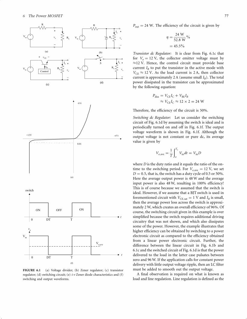
Pout ¼ 24 W. The efficiency of the circuit is given by
Z ¼24 W
52:8 W%
¼ 45:5%
Transistor dc Regulator: It is clear from Fig. 6.1c that
for Vo ¼ 12 V, the collector emitter voltage must by
�12 V. Hence, the control circuit must provide base
current IB to put the transistor in the active mode with
VCE � 12 V. As the load current is 2 A, then collector
current is approximately 2 A (assume small IB). The total
power dissipated in the transistor can be approximated
by the following equation:
Pdiss ¼ VCEIC þ VBEIB
� VCEIC � 12� 2 ¼ 24 W
Therefore, the efficiency of the circuit is 50%.
Switching dc Regulator: Let us consider the switching
circuit of Fig. 6.1d by assuming the switch is ideal and is
periodically turned on and off in Fig. 6.1f. The output
voltage waveform is shown in Fig. 6.1f. Although the
output voltage is not constant or pure dc, its average
value is given by
Vo;ave ¼1
T
ðTo
o
Vindt ¼ VinD
where D is the duty ratio and it equals the ratio of the on-
time to the switching period. For Vo;ave ¼ 12 V, we set
D ¼ 0:5, that is, the switch has a duty cycle of 0.5 or 50%.
Here the average output power is 48 W and the average
input power is also 48 W, resulting in 100% efficiency!
This is of course because we assumed that the switch is
ideal. However, if we assume that a BJT switch is used in
forementioned circuit with VCE;sat ¼ 1 V and IB is small,
then the average power loss across the switch is approxi-
mately 2 W, which creates an overall efficiency of 96%. Of
course, the switching circuit given in this example is over
simplified because the switch requires additional driving
circuitry that was not shown, and which also dissipates
some of the power. However, the example illustrates that
higher efficiency can be obtained by switching to a power
electronic circuit as compared to the efficiency obtained
from a linear power electronic circuit. Further, the
difference between the linear circuit in Fig. 6.1b and
6.1c and the switched circuit of Fig. 6.1d is that the power
delivered to the load in the latter case pulsates between
zero and 96 W. If the application calls for constant power
delivery with little output voltage ripple, then an LC filter
must be added to smooth out the output voltage.
A final observation is required on what is known as
load and line regulation. Line regulation is defined as the
(f)
i(A)
−12V
0.01
v(V)
switch
ON ONOFF
DT Tt
0
vo
DT T0
Vin
Vo,ave
t
(e)
FIGURE 6.1 (a) Voltage divider; (b) Zener regulator; (c) transistor
regulator; (d) switching circuit; (e) i-v Zener diode characteristics and (f)
switching and output waveforms.
(a) (b)
(c)(d)
Vin
R
RL
+
vo
_
IL
ControlVin
RL
+
vo
_
IL
+ vCE −
IB
Vin
R
RL
+
vo
_
VinRL
+
vo
_
ILS
6 The Power MOSFET 77
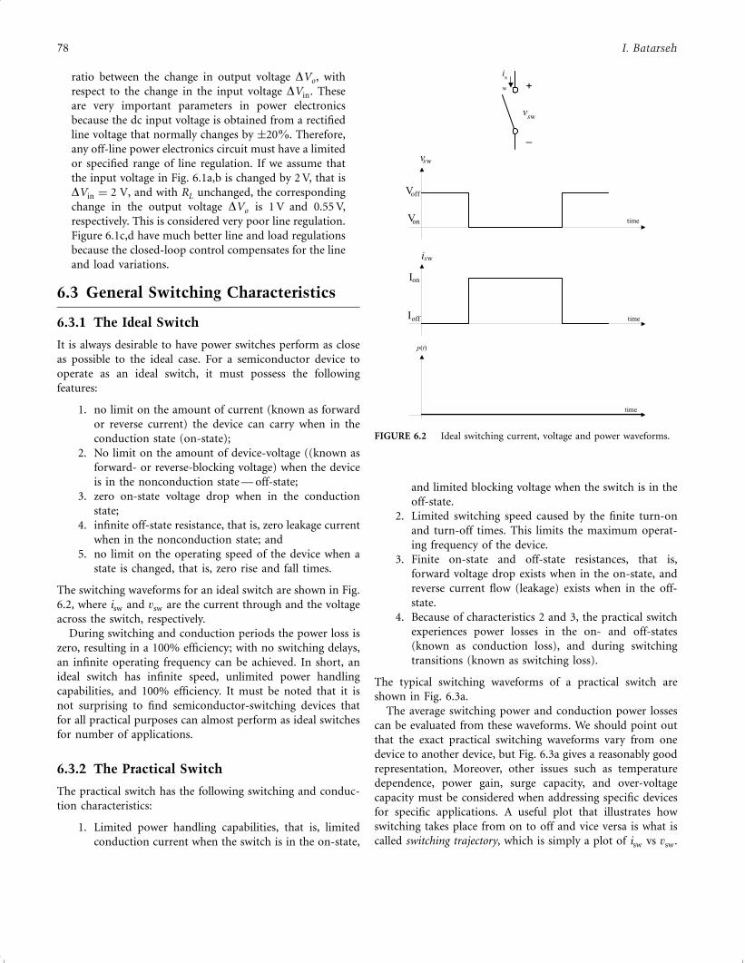
ratio between the change in output voltage DVo, with
respect to the change in the input voltage DVin. These
are very important parameters in power electronics
because the dc input voltage is obtained from a rectified
line voltage that normally changes by �20%. Therefore,
any off-line power electronics circuit must have a limited
or specified range of line regulation. If we assume that
the input voltage in Fig. 6.1a,b is changed by 2 V, that is
DVin ¼ 2 V, and with RL unchanged, the corresponding
change in the output voltage DVo is 1 V and 0.55 V,
respectively. This is considered very poor line regulation.
Figure 6.1c,d have much better line and load regulations
because the closed-loop control compensates for the line
and load variations.
6.3 General Switching Characteristics
6.3.1 The Ideal Switch
It is always desirable to have power switches perform as close
as possible to the ideal case. For a semiconductor device to
operate as an ideal switch, it must possess the following
features:
1. no limit on the amount of current (known as forward
or reverse current) the device can carry when in the
conduction state (on-state);
2. No limit on the amount of device-voltage ((known as
forward- or reverse-blocking voltage) when the device
is in the nonconduction state — off-state;
3. zero on-state voltage drop when in the conduction
state;
4. infinite off-state resistance, that is, zero leakage current
when in the nonconduction state; and
5. no limit on the operating speed of the device when a
state is changed, that is, zero rise and fall times.
The switching waveforms for an ideal switch are shown in Fig.
6.2, where isw and vsw are the current through and the voltage
across the switch, respectively.
During switching and conduction periods the power loss is
zero, resulting in a 100% efficiency; with no switching delays,
an infinite operating frequency can be achieved. In short, an
ideal switch has infinite speed, unlimited power handling
capabilities, and 100% efficiency. It must be noted that it is
not surprising to find semiconductor-switching devices that
for all practical purposes can almost perform as ideal switches
for number of applications.
6.3.2 The Practical Switch
The practical switch has the following switching and conduc-
tion characteristics:
1. Limited power handling capabilities, that is, limited
conduction current when the switch is in the on-state,
and limited blocking voltage when the switch is in the
off-state.
2. Limited switching speed caused by the finite turn-on
and turn-off times. This limits the maximum operat-
ing frequency of the device.
3. Finite on-state and off-state resistances, that is,
forward voltage drop exists when in the on-state, and
reverse current flow (leakage) exists when in the off-
state.
4. Because of characteristics 2 and 3, the practical switch
experiences power losses in the on- and off-states
(known as conduction loss), and during switching
transitions (known as switching loss).
The typical switching waveforms of a practical switch are
shown in Fig. 6.3a.
The average switching power and conduction power losses
can be evaluated from these waveforms. We should point out
that the exact practical switching waveforms vary from one
device to another device, but Fig. 6.3a gives a reasonably good
representation, Moreover, other issues such as temperature
dependence, power gain, surge capacity, and over-voltage
capacity must be considered when addressing specific devices
for specific applications. A useful plot that illustrates how
switching takes place from on to off and vice versa is what is
called switching trajectory, which is simply a plot of isw vs vsw.
+
vsw
_
is
w
vsw
Voff
Von time
isw
Ioff
Ion
time
p(t)
time
FIGURE 6.2 Ideal switching current, voltage and power waveforms.
78 I. Batarseh
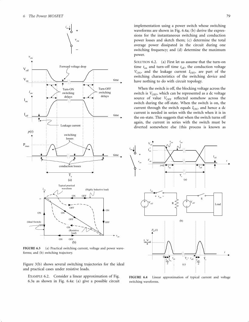
Figure 3(b) shows several switching trajectories for the ideal
and practical cases under resistive loads.
EXAMPLE 6.2. Consider a linear approximation of Fig.
6.3a as shown in Fig. 6.4a: (a) give a possible circuit
implementation using a power switch whose switching
waveforms are shown in Fig. 6.4a; (b) derive the expres-
sions for the instantaneous switching and conduction
power losses and sketch them; (c) determine the total
average power dissipated in the circuit during one
switching frequency; and (d) determine the maximum
power.
SOLUTION 6.2. (a) First let us assume that the turn-on
time ton and turn-off time toff , the conduction voltage
VON, and the leakage current IOFF, are part of the
switching characteristics of the switching device and
have nothing to do with circuit topology.
When the switch is off, the blocking voltage across the
switch is VOFF, which can be represented as a dc voltage
source of value VOFF reflected somehow across the
switch during the off-state. When the switch is on, the
current through the switch equals ION, and hence a dc
current is needed in series with the switch when it is in
the on-state. This suggests that when the switch turns off
again, the current in series with the switch must be
diverted somewhere else (this process is known as
Ts
(a)
+
vs
s
w
w
_
isw
vswVof
f
Von
isw
Ioff
Ion
ton tofft=0
t
( )t
Load
(b)
+ vsw −
isw
Voff R
P
Voff
S
(c)
IonVoff4
ton2
0 ton toff
2
TsTs− toff
t
FIGURE 6.4 Linear approximation of typical current and voltage
switching waveforms.
+
vsw
_
isw
vsw
Voff
Von time
isw
Ioff
Ion
time
p(t)
time
Pmax
Ts
Forward voltage drop
Turn-ONswitching
delays
Turn-OFFswitching
delays
Leakage current
switchinglosses
conduction losses
(a)
FIGURE 6.3 (a) Practical switching current, voltage and power wave-
forms; and (b) switching trajectory.
vsw
isw
(Ideal Switch)
(Resistiveload)
ON OFF
ON OFF
ON
OFF
ON
OFFON
OFF
Typical practicalwaveform (Highly Inductive load)
ON
ON
OFF
(b)
6 The Power MOSFET 79
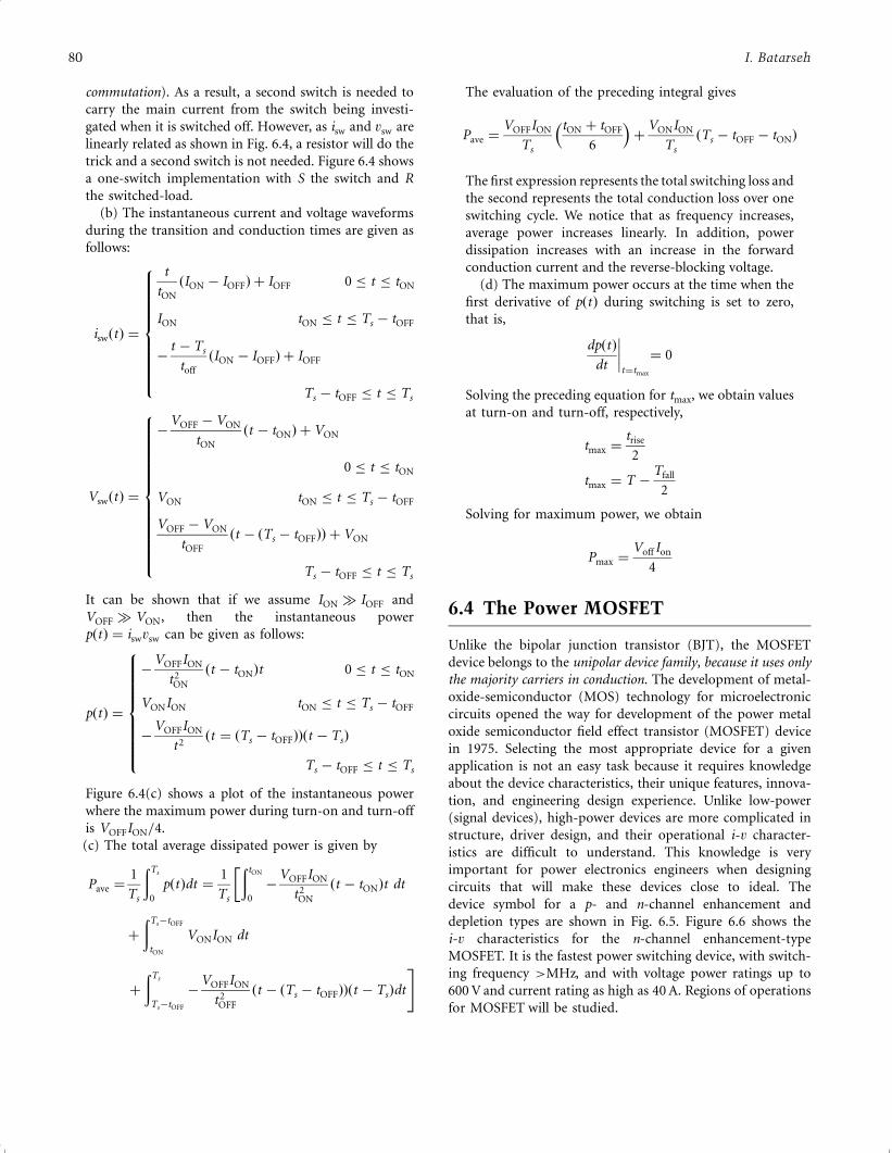
commutation). As a result, a second switch is needed to
carry the main current from the switch being investi-
gated when it is switched off. However, as isw and vsw are
linearly related as shown in Fig. 6.4, a resistor will do the
trick and a second switch is not needed. Figure 6.4 shows
a one-switch implementation with S the switch and R
the switched-load.
(b) The instantaneous current and voltage waveforms
during the transition and conduction times are given as
follows:
iswðtÞ ¼
t
tON
ðION ÿ IOFFÞ þ IOFF 0 � t � tON
ION tON � t � Ts ÿ tOFF
ÿt ÿ Ts
toff
ðION ÿ IOFFÞ þ IOFF
Ts ÿ tOFF � t � Ts
8>>>>>>>>><>>>>>>>>>:
VswðtÞ ¼
ÿVOFF ÿ VON
tON
ðt ÿ tONÞ þ VON
0 � t � tON
VON tON � t � Ts ÿ tOFF
VOFF ÿ VON
tOFF
ðt ÿ ðTs ÿ tOFFÞÞ þ VON
Ts ÿ tOFF � t � Ts
8>>>>>>>>>>>>><>>>>>>>>>>>>>:It can be shown that if we assume ION � IOFF and
VOFF � VON, then the instantaneous power
pðtÞ ¼ iswvsw can be given as follows:
pðtÞ ¼
ÿVOFFION
t2ON
ðt ÿ tONÞt 0 � t � tON
VONION tON � t � Ts ÿ tOFF
ÿVOFFION
t2ðt ¼ ðTs ÿ tOFFÞÞðt ÿ TsÞ
Ts ÿ tOFF � t � Ts
8>>>>>>>><>>>>>>>>:Figure 6.4(c) shows a plot of the instantaneous power
where the maximum power during turn-on and turn-off
is VOFFION=4.
(c) The total average dissipated power is given by
Pave ¼1
Ts
ðTs
0
pðtÞdt ¼1
Ts
ðtON
0
ÿVOFFION
t2ON
ðt ÿ tONÞt dt
�
þ
ðTsÿtOFF
tON
VONION dt
þ
ðTs
TsÿtOFF
ÿVOFFION
t2OFF
ðt ÿ ðTs ÿ tOFFÞÞðt ÿ TsÞdt
#
The evaluation of the preceding integral gives
Pave ¼VOFFION
Ts
tON þ tOFF
6
� �þ
VONION
Ts
ðTs ÿ tOFF ÿ tONÞ
The first expression represents the total switching loss and
the second represents the total conduction loss over one
switching cycle. We notice that as frequency increases,
average power increases linearly. In addition, power
dissipation increases with an increase in the forward
conduction current and the reverse-blocking voltage.
(d) The maximum power occurs at the time when the
first derivative of pðtÞ during switching is set to zero,
that is,
dpðtÞ
dt
����t¼tmax
¼ 0
Solving the preceding equation for tmax, we obtain values
at turn-on and turn-off, respectively,
tmax ¼trise
2
tmax ¼ T ÿTfall
2
Solving for maximum power, we obtain
Pmax ¼Voff Ion
4
6.4 The Power MOSFET
Unlike the bipolar junction transistor (BJT), the MOSFET
device belongs to the unipolar device family, because it uses only
the majority carriers in conduction. The development of metal-
oxide-semiconductor (MOS) technology for microelectronic
circuits opened the way for development of the power metal
oxide semiconductor field effect transistor (MOSFET) device
in 1975. Selecting the most appropriate device for a given
application is not an easy task because it requires knowledge
about the device characteristics, their unique features, innova-
tion, and engineering design experience. Unlike low-power
(signal devices), high-power devices are more complicated in
structure, driver design, and their operational i-v character-
istics are difficult to understand. This knowledge is very
important for power electronics engineers when designing
circuits that will make these devices close to ideal. The
device symbol for a p- and n-channel enhancement and
depletion types are shown in Fig. 6.5. Figure 6.6 shows the
i-v characteristics for the n-channel enhancement-type
MOSFET. It is the fastest power switching device, with switch-
ing frequency >MHz, and with voltage power ratings up to
600 V and current rating as high as 40 A. Regions of operations
for MOSFET will be studied.
80 I. Batarseh
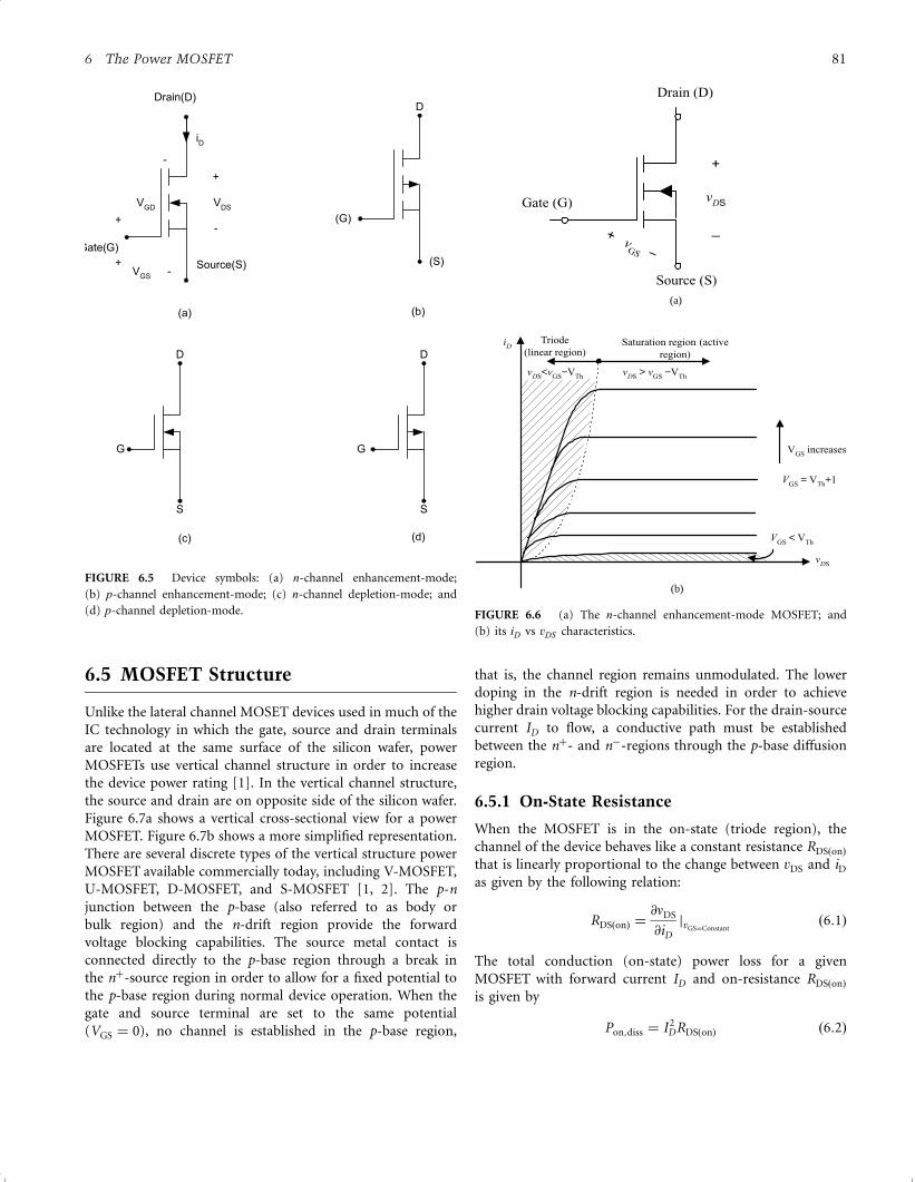
6.5 MOSFET Structure
Unlike the lateral channel MOSET devices used in much of the
IC technology in which the gate, source and drain terminals
are located at the same surface of the silicon wafer, power
MOSFETs use vertical channel structure in order to increase
the device power rating [1]. In the vertical channel structure,
the source and drain are on opposite side of the silicon wafer.
Figure 6.7a shows a vertical cross-sectional view for a power
MOSFET. Figure 6.7b shows a more simplified representation.
There are several discrete types of the vertical structure power
MOSFET available commercially today, including V-MOSFET,
U-MOSFET, D-MOSFET, and S-MOSFET [1, 2]. The p-n
junction between the p-base (also referred to as body or
bulk region) and the n-drift region provide the forward
voltage blocking capabilities. The source metal contact is
connected directly to the p-base region through a break in
the nþ-source region in order to allow for a fixed potential to
the p-base region during normal device operation. When the
gate and source terminal are set to the same potential
(VGS ¼ 0), no channel is established in the p-base region,
that is, the channel region remains unmodulated. The lower
doping in the n-drift region is needed in order to achieve
higher drain voltage blocking capabilities. For the drain-source
current ID to flow, a conductive path must be established
between the nþ- and nÿ-regions through the p-base diffusion
region.
6.5.1 On-State Resistance
When the MOSFET is in the on-state (triode region), the
channel of the device behaves like a constant resistance RDSðonÞ
that is linearly proportional to the change between vDS and iD
as given by the following relation:
RDSðonÞ ¼@nDS
@iD
jvGS¼Constantð6:1Þ
The total conduction (on-state) power loss for a given
MOSFET with forward current ID and on-resistance RDSðonÞ
is given by
Pon;diss ¼ I2DRDSðonÞ ð6:2Þ
+
vDS
_+ vGS −
Drain (D)
Source (S)
Gate (G)
vDS > vGS −VThvDS<vGS−VTh
Saturation region (activeregion)
Triode(linear region)
VGS increases
VGS = VTh+1
VGS < VTh
vDS
iD
(a)
(b)
FIGURE 6.6 (a) The n-channel enhancement-mode MOSFET; and
(b) its iD vs vDS characteristics.
+
-
iD
Gate(G)
Source(S)
VDS
VGD
+-
+-
Drain(D)
VGS
(a)
(c)
(G)
(S)
D
(b)
(d)
D
G
S
G
S
D
FIGURE 6.5 Device symbols: (a) n-channel enhancement-mode;
(b) p-channel enhancement-mode; (c) n-channel depletion-mode; and
(d) p-channel depletion-mode.
6 The Power MOSFET 81
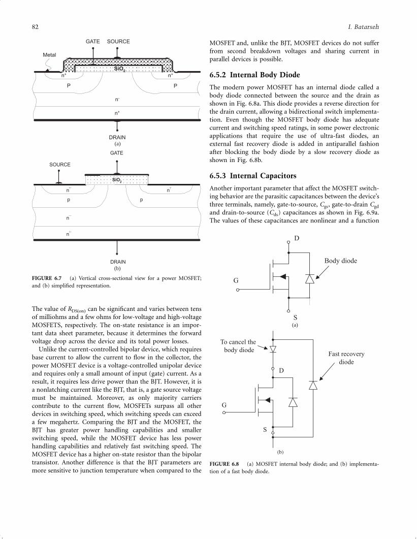
The value of RDSðonÞ can be significant and varies between tens
of milliohms and a few ohms for low-voltage and high-voltage
MOSFETS, respectively. The on-state resistance is an impor-
tant data sheet parameter, because it determines the forward
voltage drop across the device and its total power losses.
Unlike the current-controlled bipolar device, which requires
base current to allow the current to flow in the collector, the
power MOSFET device is a voltage-controlled unipolar device
and requires only a small amount of input (gate) current. As a
result, it requires less drive power than the BJT. However, it is
a nonlatching current like the BJT, that is, a gate source voltage
must be maintained. Moreover, as only majority carriers
contribute to the current flow, MOSFETs surpass all other
devices in switching speed, which switching speeds can exceed
a few megahertz. Comparing the BJT and the MOSFET, the
BJT has greater power handling capabilities and smaller
switching speed, while the MOSFET device has less power
handling capabilities and relatively fast switching speed. The
MOSFET device has a higher on-state resistor than the bipolar
transistor. Another difference is that the BJT parameters are
more sensitive to junction temperature when compared to the
MOSFET and, unlike the BJT, MOSFET devices do not suffer
from second breakdown voltages and sharing current in
parallel devices is possible.
6.5.2 Internal Body Diode
The modern power MOSFET has an internal diode called a
body diode connected between the source and the drain as
shown in Fig. 6.8a. This diode provides a reverse direction for
the drain current, allowing a bidirectional switch implementa-
tion. Even though the MOSFET body diode has adequate
current and switching speed ratings, in some power electronic
applications that require the use of ultra-fast diodes, an
external fast recovery diode is added in antiparallel fashion
after blocking the body diode by a slow recovery diode as
shown in Fig. 6.8b.
6.5.3 Internal Capacitors
Another important parameter that affect the MOSFET switch-
ing behavior are the parasitic capacitances between the device’s
three terminals, namely, gate-to-source, Cgs, gate-to-drain Cgd
and drain-to-source (Cds) capacitances as shown in Fig. 6.9a.
The values of these capacitances are nonlinear and a function
D
S
G
Body diode
(a)
FIGURE 6.8 (a) MOSFET internal body diode; and (b) implementa-
tion of a fast body diode.
n+
P
GATE SOURCE
DRAIN
SiO2
P
Metal
n+n+
n-
(a)
FIGURE 6.7 (a) Vertical cross-sectional view for a power MOSFET;
and (b) simplified representation.
nn
n
n
pp
GATE
DRAIN
SOURCE
SiO2
(b)
82 I. Batarseh
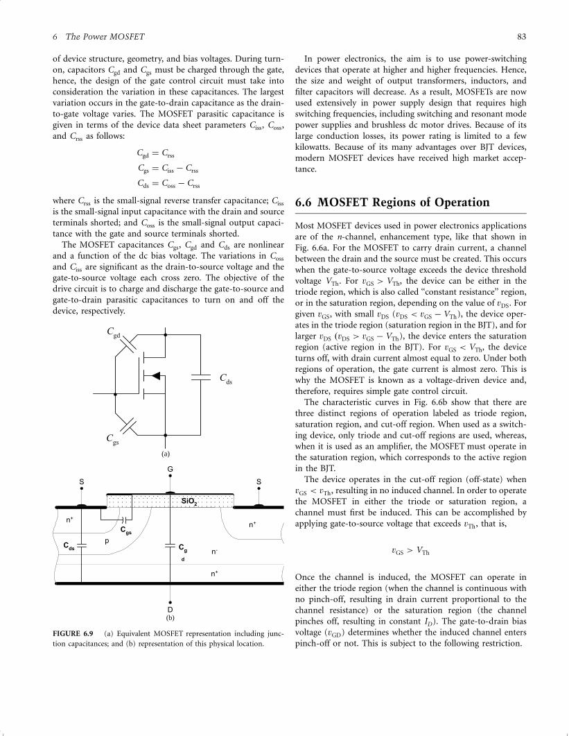
of device structure, geometry, and bias voltages. During turn-
on, capacitors Cgd and Cgs must be charged through the gate,
hence, the design of the gate control circuit must take into
consideration the variation in these capacitances. The largest
variation occurs in the gate-to-drain capacitance as the drain-
to-gate voltage varies. The MOSFET parasitic capacitance is
given in terms of the device data sheet parameters Ciss, Coss,
and Crss as follows:
Cgd ¼ Crss
Cgs ¼ Ciss ÿ Crss
Cds ¼ Coss ÿ Crss
where Crss is the small-signal reverse transfer capacitance; Ciss
is the small-signal input capacitance with the drain and source
terminals shorted; and Coss is the small-signal output capaci-
tance with the gate and source terminals shorted.
The MOSFET capacitances Cgs, Cgd and Cds are nonlinear
and a function of the dc bias voltage. The variations in Coss
and Ciss are significant as the drain-to-source voltage and the
gate-to-source voltage each cross zero. The objective of the
drive circuit is to charge and discharge the gate-to-source and
gate-to-drain parasitic capacitances to turn on and off the
device, respectively.
In power electronics, the aim is to use power-switching
devices that operate at higher and higher frequencies. Hence,
the size and weight of output transformers, inductors, and
filter capacitors will decrease. As a result, MOSFETs are now
used extensively in power supply design that requires high
switching frequencies, including switching and resonant mode
power supplies and brushless dc motor drives. Because of its
large conduction losses, its power rating is limited to a few
kilowatts. Because of its many advantages over BJT devices,
modern MOSFET devices have received high market accep-
tance.
6.6 MOSFET Regions of Operation
Most MOSFET devices used in power electronics applications
are of the n-channel, enhancement type, like that shown in
Fig. 6.6a. For the MOSFET to carry drain current, a channel
between the drain and the source must be created. This occurs
when the gate-to-source voltage exceeds the device threshold
voltage VTh. For vGS > VTh, the device can be either in the
triode region, which is also called ‘‘constant resistance’’ region,
or in the saturation region, depending on the value of vDS. For
given vGS, with small vDS (vDS < vGS ÿ VTh), the device oper-
ates in the triode region (saturation region in the BJT), and for
larger vDS ðvDS > vGS ÿ VTh), the device enters the saturation
region (active region in the BJT). For vGS < VTh, the device
turns off, with drain current almost equal to zero. Under both
regions of operation, the gate current is almost zero. This is
why the MOSFET is known as a voltage-driven device and,
therefore, requires simple gate control circuit.
The characteristic curves in Fig. 6.6b show that there are
three distinct regions of operation labeled as triode region,
saturation region, and cut-off region. When used as a switch-
ing device, only triode and cut-off regions are used, whereas,
when it is used as an amplifier, the MOSFET must operate in
the saturation region, which corresponds to the active region
in the BJT.
The device operates in the cut-off region (off-state) when
vGS < vTh, resulting in no induced channel. In order to operate
the MOSFET in either the triode or saturation region, a
channel must first be induced. This can be accomplished by
applying gate-to-source voltage that exceeds vTh, that is,
vGS > VTh
Once the channel is induced, the MOSFET can operate in
either the triode region (when the channel is continuous with
no pinch-off, resulting in drain current proportional to the
channel resistance) or the saturation region (the channel
pinches off, resulting in constant ID). The gate-to-drain bias
voltage (vGD) determines whether the induced channel enters
pinch-off or not. This is subject to the following restriction.
Cds
Cgd
Cgs
(a)
FIGURE 6.9 (a) Equivalent MOSFET representation including junc-
tion capacitances; and (b) representation of this physical location.
n+
n-
n+
n+
p
G
D
S
SiO2
S
Cg
d
Cds
Cgs
(b)
6 The Power MOSFET 83
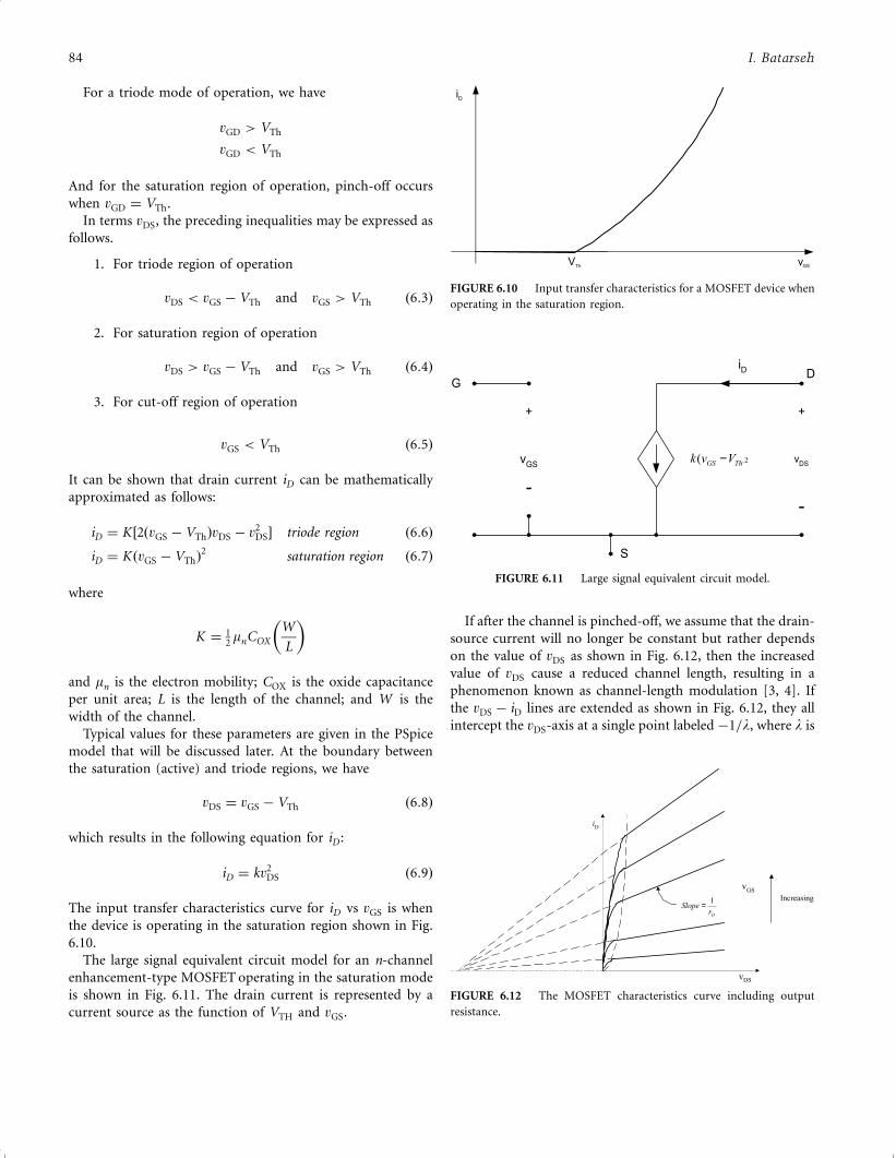
For a triode mode of operation, we have
vGD > VTh
vGD < VTh
And for the saturation region of operation, pinch-off occurs
when vGD ¼ VTh.
In terms vDS, the preceding inequalities may be expressed as
follows.
1. For triode region of operation
vDS < vGS ÿ VTh and vGS > VTh ð6:3Þ
2. For saturation region of operation
vDS > vGS ÿ VTh and vGS > VTh ð6:4Þ
3. For cut-off region of operation
vGS < VTh ð6:5Þ
It can be shown that drain current iD can be mathematically
approximated as follows:
iD ¼ K �2ðvGS ÿ VThÞvDS ÿ v2DS� triode region ð6:6Þ
iD ¼ K ðvGS ÿ VThÞ2 saturation region ð6:7Þ
where
K ¼ 12mnCOX
W
L
� �and mn is the electron mobility; COX is the oxide capacitance
per unit area; L is the length of the channel; and W is the
width of the channel.
Typical values for these parameters are given in the PSpice
model that will be discussed later. At the boundary between
the saturation (active) and triode regions, we have
vDS ¼ vGS ÿ VTh ð6:8Þ
which results in the following equation for iD :
iD ¼ kv2DS ð6:9Þ
The input transfer characteristics curve for iD vs vGS is when
the device is operating in the saturation region shown in Fig.
6.10.
The large signal equivalent circuit model for an n-channel
enhancement-type MOSFET operating in the saturation mode
is shown in Fig. 6.11. The drain current is represented by a
current source as the function of VTH and vGS.
If after the channel is pinched-off, we assume that the drain-
source current will no longer be constant but rather depends
on the value of vDS as shown in Fig. 6.12, then the increased
value of vDS cause a reduced channel length, resulting in a
phenomenon known as channel-length modulation [3, 4]. If
the vDS ÿ iD lines are extended as shown in Fig. 6.12, they all
intercept the vDS-axis at a single point labeled ÿ1=l, where l is
VTh v
iD
GS
FIGURE 6.10 Input transfer characteristics for a MOSFET device when
operating in the saturation region.
iD D
vDS
G
vGS
-
+
-
+
( Th,GS Vvk −
S
2
FIGURE 6.11 Large signal equivalent circuit model.
iD
v
IncreasingvGS
OrSlope
1=
DS
FIGURE 6.12 The MOSFET characteristics curve including output
resistance.
84 I. Batarseh
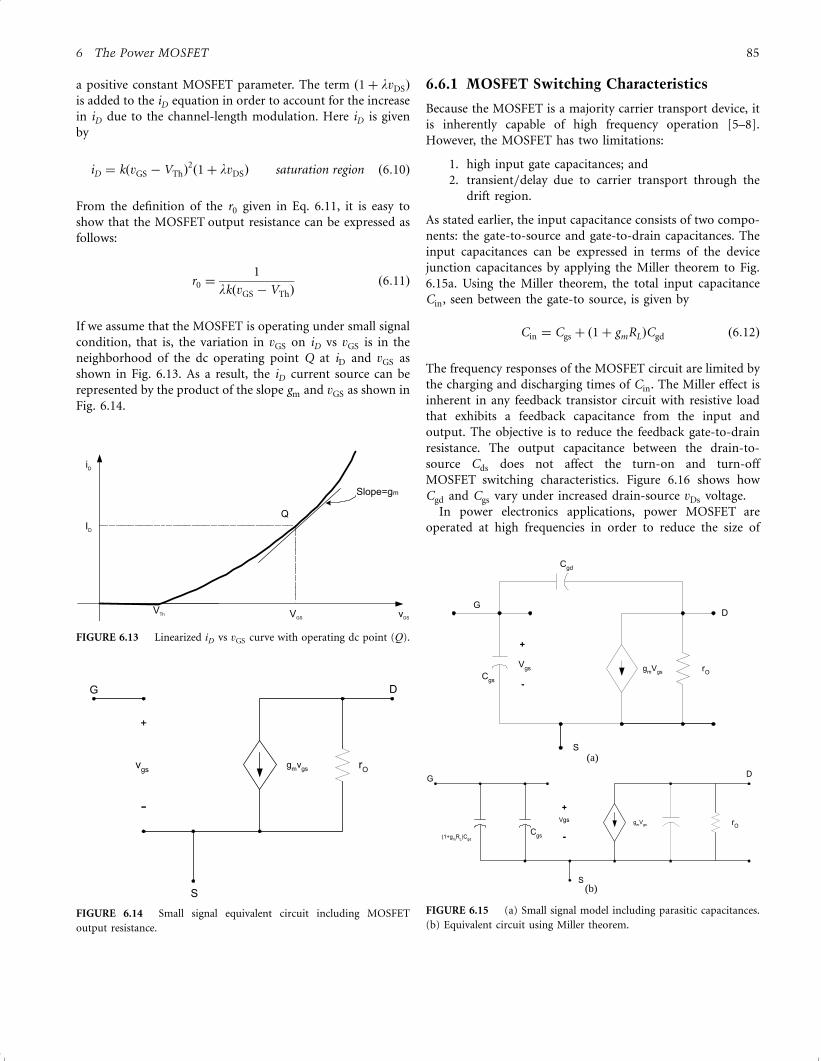
a positive constant MOSFET parameter. The term ð1þ lvDSÞ
is added to the iD equation in order to account for the increase
in iD due to the channel-length modulation. Here iD is given
by
iD ¼ kðvGS ÿ VThÞ2ð1þ lvDSÞ saturation region ð6:10Þ
From the definition of the r0 given in Eq. 6.11, it is easy to
show that the MOSFET output resistance can be expressed as
follows:
r0 ¼1
lkðvGS ÿ VThÞð6:11Þ
If we assume that the MOSFET is operating under small signal
condition, that is, the variation in vGS on iD vs vGS is in the
neighborhood of the dc operating point Q at iD and vGS as
shown in Fig. 6.13. As a result, the iD current source can be
represented by the product of the slope gm and vGS as shown in
Fig. 6.14.
6.6.1 MOSFET Switching Characteristics
Because the MOSFET is a majority carrier transport device, it
is inherently capable of high frequency operation [5–8].
However, the MOSFET has two limitations:
1. high input gate capacitances; and
2. transient=delay due to carrier transport through the
drift region.
As stated earlier, the input capacitance consists of two compo-
nents: the gate-to-source and gate-to-drain capacitances. The
input capacitances can be expressed in terms of the device
junction capacitances by applying the Miller theorem to Fig.
6.15a. Using the Miller theorem, the total input capacitance
Cin, seen between the gate-to source, is given by
Cin ¼ Cgs þ ð1þ gmRLÞCgd ð6:12Þ
The frequency responses of the MOSFET circuit are limited by
the charging and discharging times of Cin. The Miller effect is
inherent in any feedback transistor circuit with resistive load
that exhibits a feedback capacitance from the input and
output. The objective is to reduce the feedback gate-to-drain
resistance. The output capacitance between the drain-to-
source Cds does not affect the turn-on and turn-off
MOSFET switching characteristics. Figure 6.16 shows how
Cgd and Cgs vary under increased drain-source vDs voltage.
In power electronics applications, power MOSFET are
operated at high frequencies in order to reduce the size of
VTh V
GS
ID
Slope=gm
iD
Q
vGS
FIGURE 6.13 Linearized iD vs vGS curve with operating dc point (Q).
rO
D
gm
vgs
G
S
vgs
-
+
FIGURE 6.14 Small signal equivalent circuit including MOSFET
output resistance.
G
gmV
gs
Cgd
D
Vgs
Cgs
+
-
rO
S
(a)
FIGURE 6.15 (a) Small signal model including parasitic capacitances.
(b) Equivalent circuit using Miller theorem.
(1+gm
RL)C
gd
rO
S
D
Cgs
G
gmV
gsVgs
+
-
(b)
6 The Power MOSFET 85
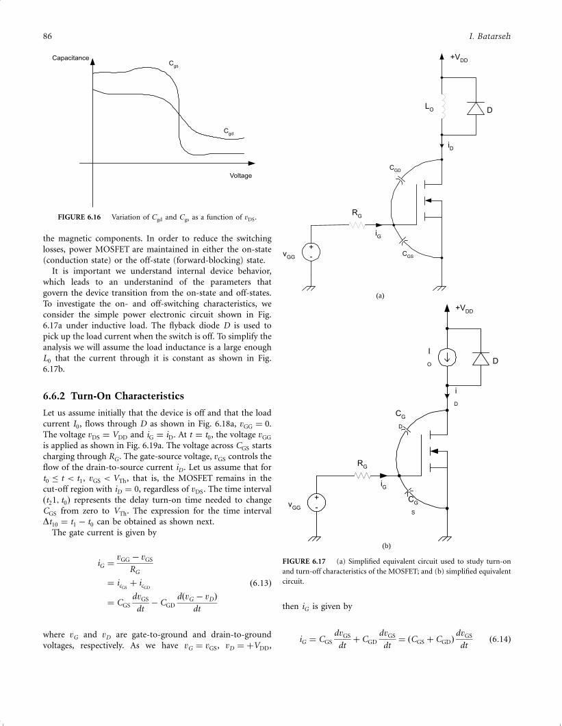
the magnetic components. In order to reduce the switching
losses, power MOSFET are maintained in either the on-state
(conduction state) or the off-state (forward-blocking) state.
It is important we understand internal device behavior,
which leads to an understanind of the parameters that
govern the device transition from the on-state and off-states.
To investigate the on- and off-switching characteristics, we
consider the simple power electronic circuit shown in Fig.
6.17a under inductive load. The flyback diode D is used to
pick up the load current when the switch is off. To simplify the
analysis we will assume the load inductance is a large enough
L0 that the current through it is constant as shown in Fig.
6.17b.
6.6.2 Turn-On Characteristics
Let us assume initially that the device is off and that the load
current I0, flows through D as shown in Fig. 6.18a, vGG ¼ 0.
The voltage vDS ¼ VDD and iG ¼ iD. At t ¼ t0, the voltage vGG
is applied as shown in Fig. 6.19a. The voltage across CGS starts
charging through RG . The gate-source voltage, vGS controls the
flow of the drain-to-source current iD . Let us assume that for
t0 � t < t1, vGS < VTh, that is, the MOSFET remains in the
cut-off region with iD ¼ 0, regardless of vDS. The time interval
ðt21; t0Þ represents the delay turn-on time needed to change
CGS from zero to VTh. The expression for the time interval
Dt10 ¼ t1 ÿ t0 can be obtained as shown next.
The gate current is given by
iG ¼vGG ÿ vGS
RG
¼ icGSþ icGD
¼ CGS
dvGS
dtÿ CGD
dðvG ÿ vDÞ
dt
ð6:13Þ
where vG and vD are gate-to-ground and drain-to-ground
voltages, respectively. As we have vG ¼ vGS, vD ¼ þVDD,
then iG is given by
iG ¼ CGS
dvGS
dtþ CGD
dvGS
dt¼ ðCGS þ CGDÞ
dvGS
dtð6:14Þ
Cgd
Cgs
Capacitance
Voltage
FIGURE 6.16 Variation of Cgd and Cgs as a function of vDS.R
G
LO D
CGS
CGD
iG
vGG
+VDD
+
-
iD
(a)
FIGURE 6.17 (a) Simplified equivalent circuit used to study turn-on
and turn-off characteristics of the MOSFET; and (b) simplified equivalent
circuit.
vGG
RG
I
OD
CG
S
CG
D
iG
+VDD
+
-
i
D
(b)
86 I. Batarseh
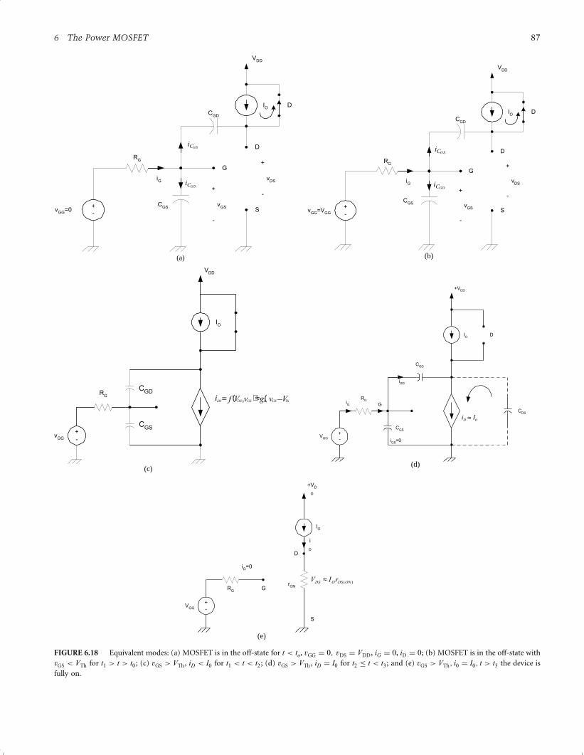
FIGURE 6.18 Equivalent modes: (a) MOSFET is in the off-state for t < to, vGG ¼ 0; vDS ¼ VDD, iG ¼ 0, iD ¼ 0; (b) MOSFET is in the off-state with
vGS < VTh for t1 > t > t0; (c) vGS > VTh, iD < I0 for t1 < t < t2; (d) vGS > VTh, iD ¼ I0 for t2 � t < t3; and (e) vGS > VTh; i0 ¼ I0; t > t3 the device is
fully on.
IO
+
-
D
G
SvGG
=0
VDD
RG
iG
D
vDS
-
+
vGS
-
+
CGD
CGS
i
i
C
C
G
G
S
D
(a)
i
i
C
C
G
G
S
D
IO
+
-
D
G
S
CGD
CGS
vGG
=VGG
VDD
RG
iG
D
vDS
-
+
vGS
-
+
(b)
+
-v
GG
VDD
RG
IO
( ) ( ThGSmGSDSDS f V g –Vi = ,v v≈C
C
GD
GS
(c)
+
-V
GG
+VDD
RG
IO
CGS
CGD
D
iG G
iGD
iGS
=0
CDS
iD Io≈
(d)
+
-
IO
D
G
S
rON
VGG
+VD
D
RG
iG=0
)(ONDSODS rI≈
i
D
(e)
6 The Power MOSFET 87
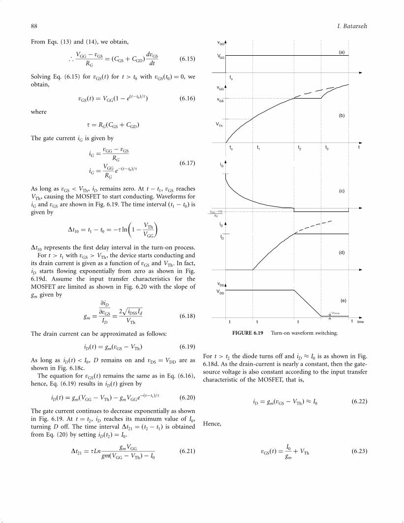
From Eqs. (13) and (14), we obtain,
;VGG ÿ vGS
RG
¼ ðCGS þ CGDÞdvGS
dtð6:15Þ
Solving Eq. (6.15) for vGSðtÞ for t > t0 with vGSðt0Þ ¼ 0, we
obtain,
vGSðtÞ ¼ VGGð1ÿ eðtÿt0Þ=tÞ ð6:16Þ
where
t ¼ RGðCGS þ CGDÞ
The gate current iG is given by
iG ¼vGG ÿ vGS
RG
iG ¼VGG
RG
eÿðtÿt0Þ=tð6:17Þ
As long as vGS < VTh, iD remains zero. At t ÿ t1, vGS reaches
VTh, causing the MOSFET to start conducting. Waveforms for
iG and vGS are shown in Fig. 6.19. The time interval ðt1 ÿ t0Þ is
given by
Dt10 ¼ t1 ÿ t0 ¼ ÿt ln 1ÿVTh
VGG
� �Dt10 represents the first delay interval in the turn-on process.
For t > t1 with vGS > VTh, the device starts conducting and
its drain current is given as a function of vGS and VTh. In fact,
iD starts flowing exponentially from zero as shown in Fig.
6.19d. Assume the input transfer characteristics for the
MOSFET are limited as shown in Fig. 6.20 with the slope of
gm given by
gm ¼
@iD
@vGS
ID
¼2�����������iDSSId
pVTh
ð6:18Þ
The drain current can be approximated as follows:
iDðtÞ ¼ gmðvGS ÿ VThÞ ð6:19Þ
As long as iDðtÞ < I0, D remains on and vDS ¼ VDD are as
shown in Fig. 6.18c.
The equation for vGSðtÞ remains the same as in Eq. (6.16),
hence, Eq. (6.19) results in iDðtÞ given by
iDðtÞ ¼ gmðVGG ÿ VThÞ ÿ gmVGGeÿðtÿt1Þ=t ð6:20Þ
The gate current continues to decrease exponentially as shown
in Fig. 6.19. At t ¼ t2, iD reaches its maximum value of I0,
turning D off. The time interval Dt21 ¼ ðt2 ÿ t1Þ is obtained
from Eq. (20) by setting iDðt2Þ ¼ I0.
Dt21 ¼ tLngmVGG
gmðVGG ÿ VThÞ ÿ I0
ð6:21Þ
For t > t2 the diode turns off and iD � I0 is as shown in Fig.
6.18d. As the drain-current is nearly a constant, then the gate-
source voltage is also constant according to the input transfer
characteristic of the MOSFET, that is,
iD ¼ gmðvGS ÿ VThÞ � I0 ð6:22Þ
Hence,
vGSðtÞ ¼I0
gm
þ VTh ð6:23Þ
vGG
VGG
to
vGG
vGS
to
VTh
t2
t1
iG
GRVThGGV −
−
iD
vDS
VDD
IOrDS(ON)
t3
t
t
(a)
(b)
(c)
(d)
(e)
t tt
IO
time
FIGURE 6.19 Turn-on waveform switching.
88 I. Batarseh
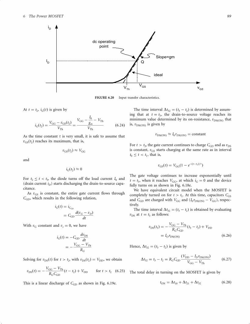
At t ¼ t2, iGðtÞ is given by
iGðt2Þ ¼VGG ÿ vGSðt2Þ
VTh
¼
VGG ÿI0
gm
ÿ VTh
VTh
ð6:24Þ
As the time constant t is very small, it is safe to assume that
vGSðt2Þ reaches its maximum, that is,
vGSðt2Þ � VGG
and
iGðt2Þ � 0
For t2 � t < t3, the diode turns off the load current I0 and
(drain current iD) starts discharging the drain-to-source capa-
citance.
As vGS is constant, the entire gate current flows through
CGD, which results in the following relation,
iGðtÞ ¼ iCGD
¼ CGD
dðvG ÿ vDÞ
dt
With vG constant and vs ¼ 0, we have
iGðtÞ ¼ ÿCGD
dvDS
dt
¼ ÿVGG ÿ VTh
RG
Solving for vDSðtÞ for t > t2, with vDSðt2Þ ¼ VDD, we obtain
vDSðtÞ ¼ ÿVGG ÿ VTh
RGCGD
ðt ÿ t2Þ þ VDD for t > t2 ð6:25Þ
This is a linear discharge of CGD as shown in Fig. 6.19e.
The time interval Dt32 ¼ ðt3 ÿ t2Þ is determined by assum-
ing that at t ¼ t3, the drain-to-source voltage reaches its
minimum value determined by its on-resistance, vDSðONÞ that
is, vDSðONÞ is given by
vDSðONÞ � I0rDSðON Þ ¼ constant
For t > t3, the gate current continues to charge CGD and as vDS
is constant, vGS starts charging at the same rate as in interval
t0 � t < t1, that is,
vGSðtÞ ¼ VGGð1ÿ eÿðtÿt3Þ=tÞ
The gate voltage continues to increase exponentially until
t ¼ t3, when it reaches VGG, at which iG ¼ 0 and the device
fully turns on as shown in Fig. 6.18e.
We have equivalent circuit model when the MOSFET is
completely turned on for t > t1. At this time, capacitors CGS
and CGD are charged with VGG and (I0rDSðONÞ ÿ VGG), respec-
tively.
The time interval Dt32 ¼ ðt3 ÿ t2Þ is obtained by evaluating
vDS at t ¼ t3 as follows:
vDSðt3Þ ¼ ÿVGG ÿ VTh
RGCGD
ðt3 ÿ t2Þ þ VDD
¼ IOrDSðONÞ ð6:26Þ
Hence, Dt32 ¼ ðt3 ÿ t2Þ is given by
Dt32 ¼ t3 ÿ t2 ¼ RGCGD
ðVDD ÿ IDrDSðONÞÞ
VGG ÿ VTh
ð6:27Þ
The total delay in turning on the MOSFET is given by
tON ¼ Dt10 þ Dt21 þ Dt32 ð6:28Þ
VTh
VGS v
GS
ID
iD
Slope=gm
ideal
dc operating
point
Q
FIGURE 6.20 Input transfer characteristics.
6 The Power MOSFET 89
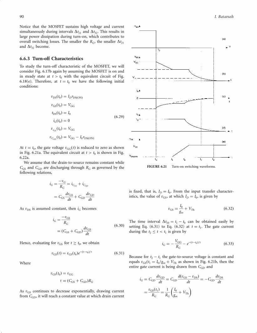
Notice that the MOSFET sustains high voltage and current
simultaneously during intervals Dt21 and Dt32. This results in
large power dissipation during turn-on, which contributes to
overall switching losses. The smaller the RG , the smaller Dt21
and Dt32 become.
6.6.3 Turn-off Characteristics
To study the turn-off characteristic of the MOSFET, we will
consider Fig. 6.17b again by assuming the MOSFET is on and
in steady state at t > t0 with the equivalent circuit of Fig.
6.18(e). Therefore, at t ¼ t0 we have the following initial
conditions:
vDSðt0Þ ¼ IDrDSðONÞ
vGSðt0Þ ¼ VGG
tDSðt0Þ ¼ I0
iGðt0Þ ¼ 0
vcGSðt0Þ ¼ VGG
vCGDðt0Þ ¼ VGG ÿ I0rDSðONÞ
ð6:29Þ
At t ¼ t0, the gate voltage vGGðtÞ is reduced to zero as shown
in Fig. 6.21a. The equivalent circuit at t > t0 is shown in Fig.
6.22a.
We assume that the drain-to-source remains constant while
CGS and CGD are discharging through RG as governed by the
following relations,
iG ¼ÿnG
RG
¼ iCGSþ iCGD
¼ CGS
dvGS
dtþ CGD
dvGD
dt
As vDS is assumed constant, then iG becomes
iG ¼ÿvGS
RG
¼ ðCGS þ CGDÞdvGS
dt
ð6:30Þ
Hence, evaluating for vGS for t � t0, we obtain
vGSðtÞ ¼ vGSðt0Þeÿðtÿt0Þ=t ð6:31Þ
Where
vGSðt0Þ ¼ vGG
t ¼ ðCGS þ CGDÞRG
As vGS continues to decrease exponentially, drawing current
from CGD, it will reach a constant value at which drain current
is fixed, that is, ID ¼ I0. From the input transfer character-
istics, the value of vGS, at which ID ¼ I0, is given by
vGS ¼I0
gm
þ VTh ð6:32Þ
The time interval Dt10 ¼ t1 ÿ t0 can be obtained easily by
setting Eq. (6.31) to Eq. (6.32) at t ¼ t1. The gate current
during the t2 � t < t1 is given by
iG ¼ ÿVGG
RG
ÿ eÿðtÿt0Þ=t ð6:33Þ
Because for t2 ÿ t1 the gate-to-source voltage is constant and
equals vGSðt1 ¼ I0=gm þ VTh as shown in Fig. 6.21b, then the
entire gate current is being drawn from CGD and
iG ¼ CGD
dvGD
dt¼ CGD
dðvGS ÿ vDSÞ
dt¼ ÿCGD
dvDS
dt
¼vGSðt1Þ
RG
¼1
RG
I0
gm
þ VTh
� �
FIGURE 6.21 Turn-on switching waveforms.
90 I. Batarseh
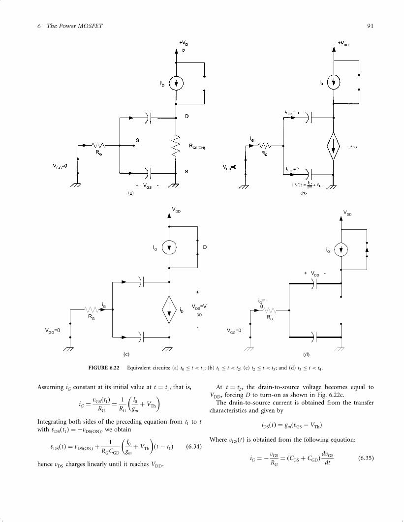
Assuming iG constant at its initial value at t ¼ t1, that is,
iG ¼vGSðt1Þ
RG
¼1
RG
I0
gm
þ VTh
� �Integrating both sides of the preceding equation from t1 to t
with vDSðt1Þ ¼ ÿvDSðONÞ, we obtain
vDSðtÞ ¼ vDSðONÞ þ1
RGCGD
I0
gm
þ VTh
� �ðt ÿ t1Þ ð6:34Þ
hence vDS charges linearly until it reaches VDD.
At t ¼ t2, the drain-to-source voltage becomes equal to
VDD, forcing D to turn-on as shown in Fig. 6.22c.
The drain-to-source current is obtained from the transfer
characteristics and given by
iDSðtÞ ¼ gmðvGS ÿ VThÞ
Where vGSðtÞ is obtained from the following equation:
iG ¼ ÿvGS
RG
¼ ðCGS þ CGDÞdvGS
dtð6:35Þ
VGG
=0
VDD
RG
IO
iG V
DS=V
DD
-
+
iD
D
VGG
=0
VDD
RG
iO
iG=
0
VDD
-+
(c) (d)
FIGURE 6.22 Equivalent circuits: (a) t0 � t < t1; (b) t1 � t < t2; (c) t2 � t < t3; and (d) t3 � t < t4.
6 The Power MOSFET 91
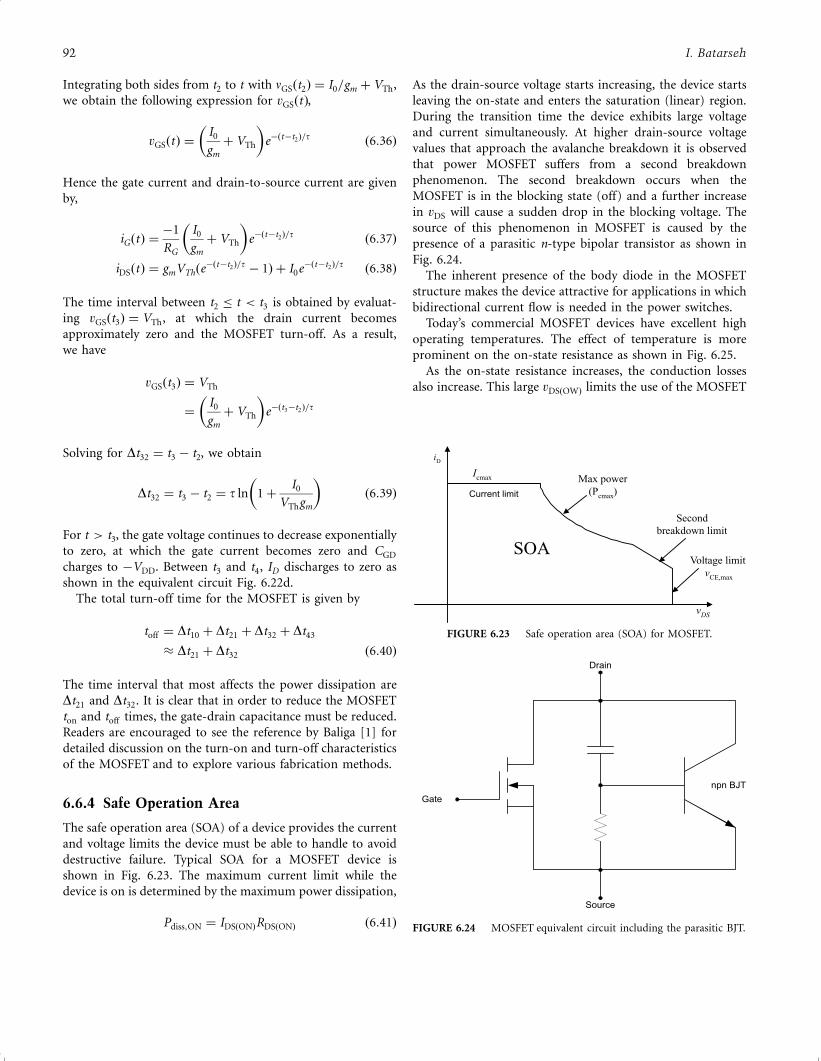
Integrating both sides from t2 to t with nGSðt2Þ ¼ I0=gm þ VTh,
we obtain the following expression for vGSðtÞ,
vGSðtÞ ¼I0
gm
þ VTh
� �eÿðtÿt2Þ=t ð6:36Þ
Hence the gate current and drain-to-source current are given
by,
iGðtÞ ¼ÿ1
RG
I0
gm
þ VTh
� �eÿðtÿt2Þ=t ð6:37Þ
iDSðtÞ ¼ gmVThðeÿðtÿt2Þ=t ÿ 1Þ þ I0eÿðtÿt2Þ=t ð6:38Þ
The time interval between t2 � t < t3 is obtained by evaluat-
ing vGSðt3Þ ¼ VTh, at which the drain current becomes
approximately zero and the MOSFET turn-off. As a result,
we have
vGSðt3Þ ¼ VTh
¼I0
gm
þ VTh
� �eÿðt3ÿt2Þ=t
Solving for Dt32 ¼ t3 ÿ t2, we obtain
Dt32 ¼ t3 ÿ t2 ¼ t ln 1þI0
VThgm
� �ð6:39Þ
For t > t3, the gate voltage continues to decrease exponentially
to zero, at which the gate current becomes zero and CGD
charges to ÿVDD. Between t3 and t4, ID discharges to zero as
shown in the equivalent circuit Fig. 6.22d.
The total turn-off time for the MOSFET is given by
toff ¼ Dt10 þ Dt21 þ Dt32 þ Dt43
� Dt21 þ Dt32 ð6:40Þ
The time interval that most affects the power dissipation are
Dt21 and Dt32. It is clear that in order to reduce the MOSFET
ton and toff times, the gate-drain capacitance must be reduced.
Readers are encouraged to see the reference by Baliga [1] for
detailed discussion on the turn-on and turn-off characteristics
of the MOSFET and to explore various fabrication methods.
6.6.4 Safe Operation Area
The safe operation area (SOA) of a device provides the current
and voltage limits the device must be able to handle to avoid
destructive failure. Typical SOA for a MOSFET device is
shown in Fig. 6.23. The maximum current limit while the
device is on is determined by the maximum power dissipation,
Pdiss;ON ¼ IDSðONÞRDSðONÞ ð6:41Þ
As the drain-source voltage starts increasing, the device starts
leaving the on-state and enters the saturation (linear) region.
During the transition time the device exhibits large voltage
and current simultaneously. At higher drain-source voltage
values that approach the avalanche breakdown it is observed
that power MOSFET suffers from a second breakdown
phenomenon. The second breakdown occurs when the
MOSFET is in the blocking state (off) and a further increase
in vDS will cause a sudden drop in the blocking voltage. The
source of this phenomenon in MOSFET is caused by the
presence of a parasitic n-type bipolar transistor as shown in
Fig. 6.24.
The inherent presence of the body diode in the MOSFET
structure makes the device attractive for applications in which
bidirectional current flow is needed in the power switches.
Today’s commercial MOSFET devices have excellent high
operating temperatures. The effect of temperature is more
prominent on the on-state resistance as shown in Fig. 6.25.
As the on-state resistance increases, the conduction losses
also increase. This large vDSðOWÞ limits the use of the MOSFET
iD
vDS
SOA
Current limit
Icmax Max power(Pcmax)
Secondbreakdown limit
Voltage limitvCE,max
FIGURE 6.23 Safe operation area (SOA) for MOSFET.
Drain
Gate
Source
npn BJT
FIGURE 6.24 MOSFET equivalent circuit including the parasitic BJT.
92 I. Batarseh
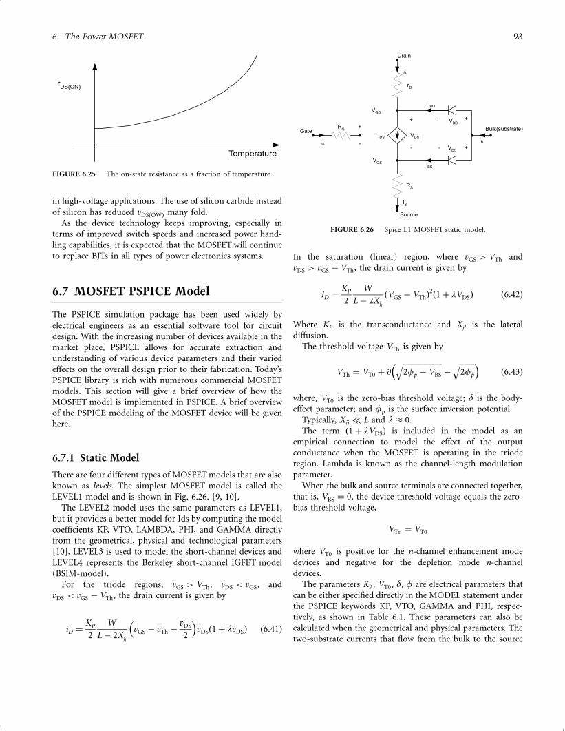
in high-voltage applications. The use of silicon carbide instead
of silicon has reduced vDSðOWÞ many fold.
As the device technology keeps improving, especially in
terms of improved switch speeds and increased power hand-
ling capabilities, it is expected that the MOSFET will continue
to replace BJTs in all types of power electronics systems.
6.7 MOSFET PSPICE Model
The PSPICE simulation package has been used widely by
electrical engineers as an essential software tool for circuit
design. With the increasing number of devices available in the
market place, PSPICE allows for accurate extraction and
understanding of various device parameters and their varied
effects on the overall design prior to their fabrication. Today’s
PSPICE library is rich with numerous commercial MOSFET
models. This section will give a brief overview of how the
MOSFET model is implemented in PSPICE. A brief overview
of the PSPICE modeling of the MOSFET device will be given
here.
6.7.1 Static Model
There are four different types of MOSFET models that are also
known as levels. The simplest MOSFET model is called the
LEVEL1 model and is shown in Fig. 6.26. [9, 10].
The LEVEL2 model uses the same parameters as LEVEL1,
but it provides a better model for Ids by computing the model
coefficients KP, VTO, LAMBDA, PHI, and GAMMA directly
from the geometrical, physical and technological parameters
[10]. LEVEL3 is used to model the short-channel devices and
LEVEL4 represents the Berkeley short-channel IGFET model
(BSIM-model).
For the triode regions, vGS > VTh, vDS < vGS, and
vDS < vGS ÿ VTh, the drain current is given by
iD ¼KP
2
W
L ÿ 2Xjl
vGS ÿ vTh ÿvDS
2
� �vDSð1þ lvDSÞ ð6:41Þ
In the saturation (linear) region, where vGS > VTh and
vDS > vGS ÿ VTh, the drain current is given by
ID ¼KP
2
W
L ÿ 2Xjl
ðVGS ÿ VThÞ2ð1þ lVDSÞ ð6:42Þ
Where KP is the transconductance and Xjl is the lateral
diffusion.
The threshold voltage VTh is given by
VTh ¼ VT0 þ @���������������������2fp ÿ VBS
qÿ
��������2fp
q� �ð6:43Þ
where, VT0 is the zero-bias threshold voltage; d is the body-
effect parameter; and fp is the surface inversion potential.
Typically, Xij � L and l � 0.
The term ð1þ lVDSÞ is included in the model as an
empirical connection to model the effect of the output
conductance when the MOSFET is operating in the triode
region. Lambda is known as the channel-length modulation
parameter.
When the bulk and source terminals are connected together,
that is, VBS ¼ 0, the device threshold voltage equals the zero-
bias threshold voltage,
VTn ¼ VT0
where VT0 is positive for the n-channel enhancement mode
devices and negative for the depletion mode n-channel
devices.
The parameters KP, VT0, d, f are electrical parameters that
can be either specified directly in the MODEL statement under
the PSPICE keywords KP, VTO, GAMMA and PHI, respec-
tively, as shown in Table 6.1. These parameters can also be
calculated when the geometrical and physical parameters. The
two-substrate currents that flow from the bulk to the source
rDS(ON)
Temperature
FIGURE 6.25 The on-state resistance as a fraction of temperature.
-
Gate
Source
VDS
VGD
+
-
+
Drain
VGS
Bulk(substrate)iDS
VBD
VBS
-
+
- +
RG
iG
rD
RS
iBD
iBS
iB
IS
iD
FIGURE 6.26 Spice L1 MOSFET static model.
6 The Power MOSFET 93
IBS and from the bulk to the drain IBD are simply diode
currents and are given by
IBS ¼ ISS eÿ
VBSVT ÿ 1
� �ð6:44Þ
IBD ¼ IDS eÿ
VBDVT ÿ 1
� �ð6:45Þ
Where ISS and IDS are the substrate source and substrate drain
saturation currents. These currents are considered equal and
given as IS in the MODEL statement with a default value of
10ÿ14 A. Where the equation symbols and their corresponding
PSpice parameter names are shown in Table 6.1.
In PSpice, a MOSFET device is described by two statements,
with first statement starting with the letter M and the second
statement starting with .Model, which defines the model used
in the first statement. The following syntax is used:
M<device_name> <Drain_node_number>
Gate_node_number>
<Source_node_number> <Substrate_node
number> <Model_name> *
[<param_1>=<value_1>
<param_2>=<value_>....] .MODEL
<Model_name> <type_name>
[ (<param_1>=<value_1>
<param_2>=<value_2> .....]
Where the starting letter "M" in M<devic_name> state-
ment indicates that the device is a MOSFET and <device_
name> is a user specified label for the given device, the
<Model_name> is one of the hundreds of device models
specified in the PSpice library; and <model_name> or the
same name specified in the device name statement <type_
name>, is either NMOS of PMOS, depending on whether the
device is n- or p-channel MOS, respectively. An optional list of
parameter types and their values follows. Length L and width
W and other parameters can be specified in the M<device_
name>, in the .MODEL or .OPTION statements. A user may
select not to include any value, and PSpice will use the specified
default values in the model. For normal operation (physical
construction of the MOS devices), the source and bulk substrate
nodes must be connected together. In all the PSpice library files,
defaultparameter values for L,W,AS,AD,PS,PD,NRD,andNDS
are included, and a user then should not specify such values in the
device ‘‘M’’ statement or in the OPTION statement.
The power MOSFET device PSpice models include relatively
complete static and dynamic device characteristics given in the
manufacturing data sheet. In general, the following effects are
specified in a given PSpice model: dc transfer curves, on-
resistance, switching delays, gate dive characteristics, and
reverse-mode ‘‘body-diode’’ operation. The device character-
istics that are not included in the model are noise, latch-ups,
maximum voltage, and power ratings. Please see OrCAD
Library Files.
EXAMPLE 6.3. Let us consider an example that uses IRF
MOSFET and connected as shown in Fig. 6.27.
It was decided that the device should have a blocking
voltage (VDSS) of 600 V and drain current id of 3.6 A. The
device selected is IRF CC30 with case TO220. This device is
listed in the PSpice library under model number IRFBC30 as
follows:
*Library of Power MOSFET Models *Copyright
OrCAD, Inc. 1998 All Rights Reserved. *
*$Revision: 1.24 $ *$Author: Rperez $
*$Date: 19 October 1998 10:22:26 $ * .
Model IRFBC30 NMOS NMOS
The PSpice code for the MOS device labeled S1 used in Fig.
6.27 is given by
MS1 3 5 0 0 IRFBC30 .MODEL IRFBC30
.Model IRFBC30 NMOS(Level=3 Gamma=0
Delta=0 Eta=0 Theta=0 Kappa=0.2
Vmax=0 Xj=0 + Tox=100n Uo=600 Phi=.6
Rs=5.002m Kp=20.43u W=.35 L=2u
Vto=3.625 + Rd=1.851 Rds=2.667MEG
Cbd=790.1p Pb=.8 Mj=.5 Fc=.5
Cgso=1.64n + Cgdo=123.9p Rg=1.052
Is=720.2p N=1 Tt=685) * Int'l Recti®er
pid=IRFCC30 case=TO220
6.7.2 Large Signal Model
The equivalent circuit of Fig. 6.28 includes five device parasitic
capacitances. The capacitors CGB, CGS, and CGD, represent the
charge-storage effect between the gate terminal and the bulk,
source and drain terminals, respectively. These are nonlinear
two-terminal capacitors expressed as functions of W, L Cox,
VGS, VT0, VDS, and CGB0, CGSO, CGDO. Capacitors CGB0, CGS0,
and CGD0 outside the channel region, are known as overlap
capacitances that exist between the gate electrode and the
other three terminals, respectively. Table 6.2 shows the list of
MOSFET capacitance parameters and their default values.
Notice that the PSpice overlap capacitor keywords (CGB0,
CGSO, CGDO) are proportional either to the MOSFET width
or length of the channel as follows:
CGBO ¼ CGBO=L
CGSO ¼ CGSO=W
CGDO ¼ CGDO=W
ð6:46Þ
In the triode region, where vGS > vDS ÿ VTh, the terminal
capacitors are given by,
CGS ¼ LW CoX
�1ÿ
vGS ÿ vDS ÿ VTh
2ðvGS ÿ VThÞ ÿ VDS
� �2�þ CGS0:
CGD ¼ LW CoX
�1ÿ
vGS ÿ VTh
2ðvGS ÿ VThðÿvDS
� �2�þ CGDO:
CGB ¼ CGB0L
ð6:47Þ
94 I. Batarseh
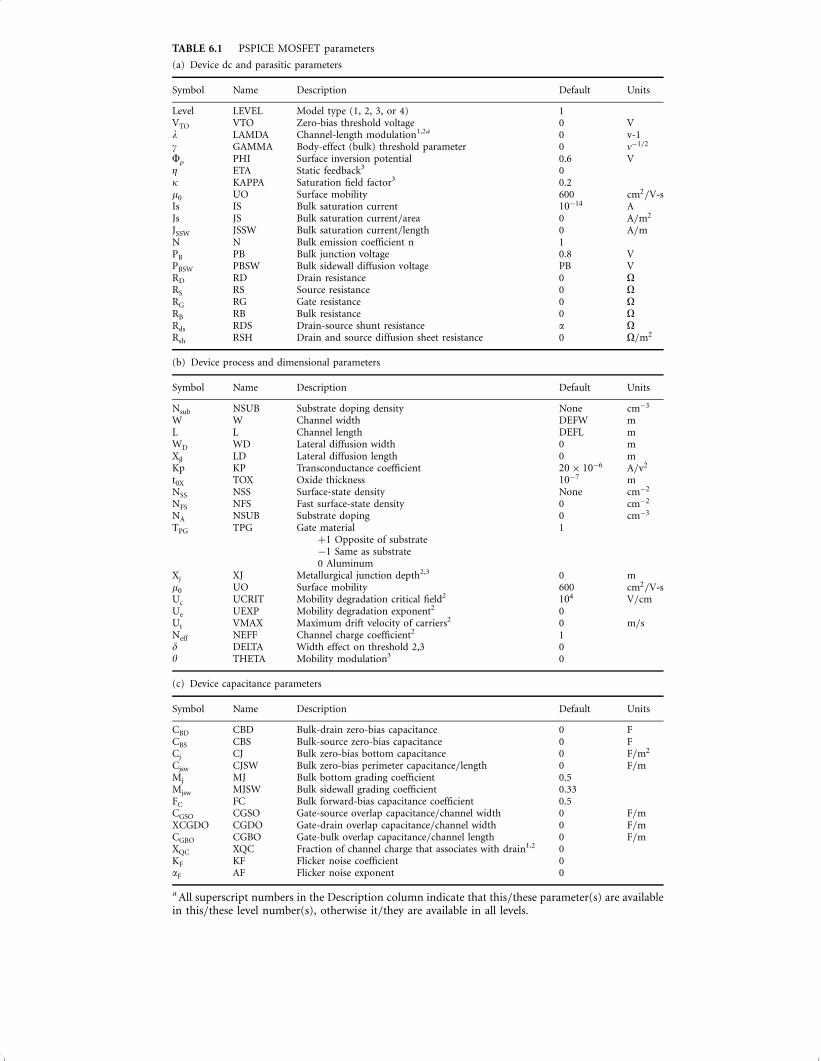
TABLE 6.1 PSPICE MOSFET parameters
(a) Device dc and parasitic parameters
Symbol Name Description Default Units
Level LEVEL Model type (1, 2, 3, or 4) 1VTO VTO Zero-bias threshold voltage 0 Vl LAMDA Channel-length modulation1,2a 0 v-1g GAMMA Body-effect (bulk) threshold parameter 0 vÿ1=2
Fr PHI Surface inversion potential 0.6 VZ ETA Static feedback3 0k KAPPA Saturation field factor3 0.2m0 UO Surface mobility 600 cm2=V-sIs IS Bulk saturation current 10ÿ14 AJs JS Bulk saturation current=area 0 A=m2
JSSW JSSW Bulk saturation current=length 0 A=mN N Bulk emission coefficient n 1PB PB Bulk junction voltage 0.8 VPBSW PBSW Bulk sidewall diffusion voltage PB VRD RD Drain resistance 0 ORS RS Source resistance 0 ORG RG Gate resistance 0 ORB RB Bulk resistance 0 ORds RDS Drain-source shunt resistance a ORsh RSH Drain and source diffusion sheet resistance 0 O=m2
(b) Device process and dimensional parameters
Symbol Name Description Default Units
Nsub NSUB Substrate doping density None cmÿ3
W W Channel width DEFW mL L Channel length DEFL mWD WD Lateral diffusion width 0 mXjl LD Lateral diffusion length 0 mKp KP Transconductance coefficient 20� 10ÿ6 A=v2
t0X TOX Oxide thickness 10ÿ7 mNSS NSS Surface-state density None cmÿ2
NFS NFS Fast surface-state density 0 cmÿ2
NA NSUB Substrate doping 0 cmÿ3
TPG TPG Gate material 1þ1 Opposite of substrateÿ1 Same as substrate0 Aluminum
Xj XJ Metallurgical junction depth2,3 0 mm0 UO Surface mobility 600 cm2=V-sUc UCRIT Mobility degradation critical field2 104 V=cmUe UEXP Mobility degradation exponent2 0Ut VMAX Maximum drift velocity of carriers2 0 m=sNeff NEFF Channel charge coefficient2 1d DELTA Width effect on threshold 2,3 0y THETA Mobility modulation3 0
(c) Device capacitance parameters
Symbol Name Description Default Units
CBD CBD Bulk-drain zero-bias capacitance 0 FCBS CBS Bulk-source zero-bias capacitance 0 FCj CJ Bulk zero-bias bottom capacitance 0 F=m2
Cjsw CJSW Bulk zero-bias perimeter capacitance=length 0 F=mMj MJ Bulk bottom grading coefficient 0.5Mjsw MJSW Bulk sidewall grading coefficient 0.33FC FC Bulk forward-bias capacitance coefficient 0.5CGSO CGSO Gate-source overlap capacitance=channel width 0 F=mXCGDO CGDO Gate-drain overlap capacitance=channel width 0 F=mCGBO CGBO Gate-bulk overlap capacitance=channel length 0 F=mXQC XQC Fraction of channel charge that associates with drain1,2 0KF KF Flicker noise coefficient 0aF AF Flicker noise exponent 0
a All superscript numbers in the Description column indicate that this=these parameter(s) are availablein this=these level number(s), otherwise it=they are available in all levels.
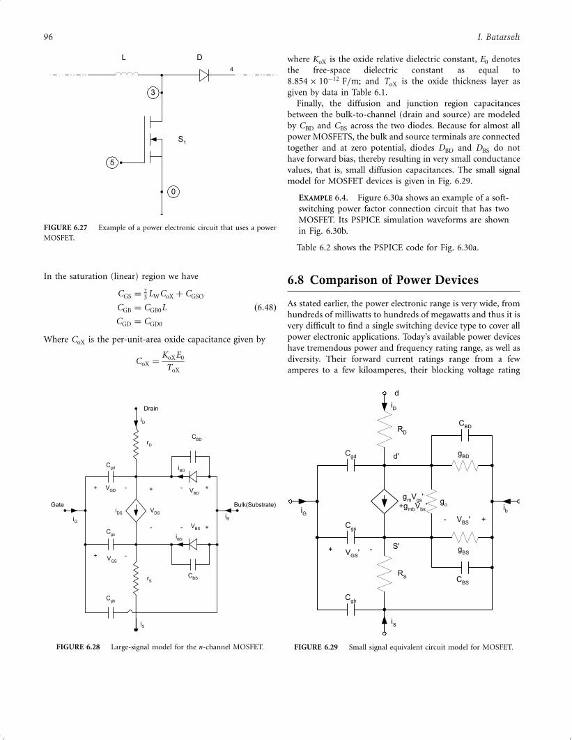
In the saturation (linear) region we have
CGS ¼23
LWCoX þ CGSO
CGB ¼ CGB0L
CGD ¼ CGD0
ð6:48Þ
Where CoX is the per-unit-area oxide capacitance given by
CoX ¼KoXE0
ToX
where KoX is the oxide relative dielectric constant, E0 denotes
the free-space dielectric constant as equal to
8:854� 10ÿ12 F=m; and ToX is the oxide thickness layer as
given by data in Table 6.1.
Finally, the diffusion and junction region capacitances
between the bulk-to-channel (drain and source) are modeled
by CBD and CBS across the two diodes. Because for almost all
power MOSFETS, the bulk and source terminals are connected
together and at zero potential, diodes DBD and DBS do not
have forward bias, thereby resulting in very small conductance
values, that is, small diffusion capacitances. The small signal
model for MOSFET devices is given in Fig. 6.29.
EXAMPLE 6.4. Figure 6.30a shows an example of a soft-
switching power factor connection circuit that has two
MOSFET. Its PSPICE simulation waveforms are shown
in Fig. 6.30b.
Table 6.2 shows the PSPICE code for Fig. 6.30a.
6.8 Comparison of Power Devices
As stated earlier, the power electronic range is very wide, from
hundreds of milliwatts to hundreds of megawatts and thus it is
very difficult to find a single switching device type to cover all
power electronic applications. Today’s available power devices
have tremendous power and frequency rating range, as well as
diversity. Their forward current ratings range from a few
amperes to a few kiloamperes, their blocking voltage rating
S1
4
DL
5
0
3
FIGURE 6.27 Example of a power electronic circuit that uses a power
MOSFET.
+ -
GateV
DS
VGD
+
-+
-
Drain
VGS
Bulk(Substrate)iDS
VBD
VBS-
+
- +
iD
iG
rD
rS
CBD
CBS
iB
iS
iBD
iBS
Cgd
Cgs
Cgb
FIGURE 6.28 Large-signal model for the n-channel MOSFET.
gm
Vgs
'
+gmb
Vbs
'
-+
d
VGS
'
VBS
'- +
iD
iG
RD
RS
CBD
CBS
ib
iS
gBD
gBS
Cgd
Cgs
Cgb
d'
S'
go
FIGURE 6.29 Small signal equivalent circuit model for MOSFET.
96 I. Batarseh

TABLE 6.2 PSPICE MOSFET capacitance parameters and their default values for Figure 6.30a
* source ZVT-ZCS
D_Do N00111 OUT Dbreak
V_Vs N00105 9 DC 0 AC 0 PULSE 0.9.0.0.0 {D*Ts} {Ts}
L_Ls 0 N00111 {n*.16}
Kn_K1 L_Lp1 L_Lp2 L_Ls 0.995
C_Co OUT 0 70uF IC=50
V_Vin N00103 0 110
L_Li N00103 N00099 17.6u IC=0
V_Va N-109 0 DC 0 AC 0 PULSE 0 9 {-Delta*Ts/1.1} 0 0 {2.0*Delta*Ts}
{Ts}
D_Dp N00121 N00169 Dbreak
C_C7 N00111 OUT 30p
R_Ro OUT 0 25
C_C8 N00143 OUT 10p
D_Dao N00143 OUT Dbreak
D_Di N00099 N00245 Dbreak
L_Lp2 N00121 0 {n} IC=0
C_C9 N00169 N00121 10p
L_Las N00143 0 {0.4*n1}
Kn_K2 L_Lap L_Las 1.0
L_Lp1 N00245 N00169 {n} IC=0
L_Lap N00245 N000791 {n1}
C_Cp2 N00245 N00121 47u IC=170
C_Cp1 N00169 0 47u IC=170
L_Lak N000791 N000911 5u IC=0
M_M1 N000911 N00109 0 0 IRFBC30
M_M2 N00245 N00105 0 0 IRF840
.PARAM D=0.3 DELTA=0.1 N1=400u N=1mH TS=2us
**** MOSFET MODEL PARAMETERS
IRFBC30 IRF840
NMOS NMOS
LEVEL 3 3
L 2.000000-06 2.000000-06
W .35 .68
VTO 3.625 3.879
KP 20.430000E-06 20.850000E-06
GAMMA 0 0
PHI .6 .6
LAMBDA 0 0
RD 1.851 .6703
RS 5.002000E-03 6.382000E-03
RG 1.052 .6038
RDS 2.667000E+06 2.222000E+06
IS 720.200000E-12 56.030000E-12
JS 0 0
PB .8 .8
PBSW .8 .8
CBD 790.100000E-12 1.415000E-09
CJ 0 0
CJSW 0 0
TT 685.000000E-09 710.000000E-09
CGSO 1.640000E-09 1.625000E-09
CGDO 123.900000E-12 133.400000E-12
CGBO 0 0
TOX 100.000000E-09 100.000000E-09
XJ 0 0
UCRIT 10.000000E+03 10.000000E+03
DELTA 0 0
ETA 0 0
DIOMOD 1 1
VFB 0 0
LETA 0 0
WETA 0 0
U0 0 0
TEMP 0 0
VDD 0 0
XPART 0 0
6 The Power MOSFET 97
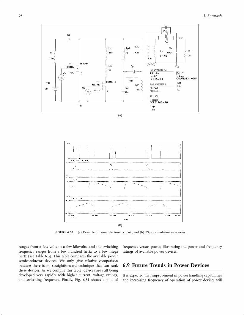
ranges from a few volts to a few kilovolts, and the switching
frequency ranges from a few hundred hertz to a few mega
hertz (see Table 6.3). This table compares the available power
semiconductor devices. We only give relative comparison
because there is no straightforward technique that can rank
these devices. As we compile this table, devices are still being
developed very rapidly with higher current, voltage ratings,
and switching frequency. Finally, Fig. 6.31 shows a plot of
frequency versus power, illustrating the power and frequency
ratings of available power devices.
6.9 Future Trends in Power Devices
It is expected that improvement in power handling capabilities
and increasing frequency of operation of power devices will
(a)
(b)
FIGURE 6.30 (a) Example of power electronic circuit; and (b) PSpice simulation waveforms.
98 I. Batarseh
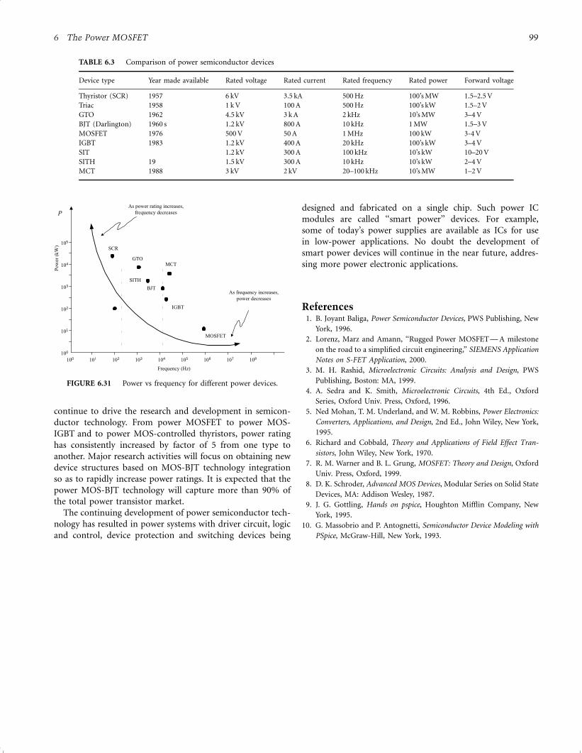
continue to drive the research and development in semicon-
ductor technology. From power MOSFET to power MOS-
IGBT and to power MOS-controlled thyristors, power rating
has consistently increased by factor of 5 from one type to
another. Major research activities will focus on obtaining new
device structures based on MOS-BJT technology integration
so as to rapidly increase power ratings. It is expected that the
power MOS-BJT technology will capture more than 90% of
the total power transistor market.
The continuing development of power semiconductor tech-
nology has resulted in power systems with driver circuit, logic
and control, device protection and switching devices being
designed and fabricated on a single chip. Such power IC
modules are called ‘‘smart power’’ devices. For example,
some of today’s power supplies are available as ICs for use
in low-power applications. No doubt the development of
smart power devices will continue in the near future, addres-
sing more power electronic applications.
References1. B. Joyant Baliga, Power Semiconductor Devices, PWS Publishing, New
York, 1996.
2. Lorenz, Marz and Amann, ‘‘Rugged Power MOSFET — A milestone
on the road to a simplified circuit engineering,’’ SIEMENS Application
Notes on S-FET Application, 2000.
3. M. H. Rashid, Microelectronic Circuits: Analysis and Design, PWS
Publishing, Boston: MA, 1999.
4. A. Sedra and K. Smith, Microelectronic Circuits, 4th Ed., Oxford
Series, Oxford Univ. Press, Oxford, 1996.
5. Ned Mohan, T. M. Underland, and W. M. Robbins, Power Electronics:
Converters, Applications, and Design, 2nd Ed., John Wiley, New York,
1995.
6. Richard and Cobbald, Theory and Applications of Field Effect Tran-
sistors, John Wiley, New York, 1970.
7. R. M. Warner and B. L. Grung, MOSFET: Theory and Design, Oxford
Univ. Press, Oxford, 1999.
8. D. K. Schroder, Advanced MOS Devices, Modular Series on Solid State
Devices, MA: Addison Wesley, 1987.
9. J. G. Gottling, Hands on pspice, Houghton Mifflin Company, New
York, 1995.
10. G. Massobrio and P. Antognetti, Semiconductor Device Modeling with
PSpice, McGraw-Hill, New York, 1993.
Pow
er(k
W)
Frequency (Hz)
As frequency increases,power decreases
100
SCR
GTOMCT
SITH
BJT
IGBT
MOSFET
As power rating increases,frequency decreases
101
102
103
100 101 102 103 104 105 106 107
104
105
108
P
FIGURE 6.31 Power vs frequency for different power devices.
TABLE 6.3 Comparison of power semiconductor devices
Device type Year made available Rated voltage Rated current Rated frequency Rated power Forward voltage
Thyristor (SCR) 1957 6 kV 3.5 kA 500 Hz 100’s MW 1.5–2.5 V
Triac 1958 1 k V 100 A 500 Hz 100’s kW 1.5–2 V
GTO 1962 4.5 kV 3 k A 2 kHz 10’s MW 3–4 V
BJT (Darlington) 1960 s 1.2 kV 800 A 10 kHz 1 MW 1.5–3 V
MOSFET 1976 500 V 50 A 1 MHz 100 kW 3-4 V
IGBT 1983 1.2 kV 400 A 20 kHz 100’s kW 3–4 V
SIT 1.2 kV 300 A 100 kHz 10’s kW 10–20 V
SITH 19 1.5 kV 300 A 10 kHz 10’s kW 2–4 V
MCT 1988 3 kV 2 kV 20–100 kHz 10’s MW 1–2 V
6 The Power MOSFET 99
7Insulated Gate Bipolar
Transistor
S. AbedinpourDepartment of Electrical
Engineering and Computer
Science
University of Illinois at
Chicago, Illinois 6067 USA
K. Shenai851 South Morgan Street
(M/C 154)
Chicago, Illinois 60607-7053
USA
7.1 Introduction
The insulated gate bipolar transistor (IGBT), which was
introduced in the early 1980s, has become a successful
device because of its superior characteristics. The IGBT is a
three-terminal power semiconductor switch used to control
electrical energy and many new applications would not be
economically feasible without IGBTs. Prior to the advent of
the IGBT, power bipolar junction transistors (BJTs) and power
metal oxide field effect transistors (MOSFETs) were widely
used in low to medium power and high-frequency applica-
tions, where the speed of gate turn-off thyristors was not
adequate. Power BJTs have good on-state characteristics but
long switching times especially at turn-off. They are current-
controlled devices with small current gain because of high-
level injection effects and wide basewidth required to prevent
reach-through breakdown for high blocking voltage capability.
Therefore, they require complex base-drive circuits to provide
the base current during on-state, which increases the power
loss in the control electrode.
On the other hand, power MOSFETs are voltage-controlled
devices, which require very small current during the switching
period and hence have simple gate-drive requirements. Power
MOSFETs are majority carrier devices, which exhibit very high
switching speeds. However, the unipolar nature of the power
MOSFETs causes inferior conduction characteristics as the
voltage rating is increased above 200 V. Therefore, their on-
state resistance increases with increasing breakdown voltage.
Furthermore, as the voltage rating increases, the inherent body
diode shows inferior reverse recovery characteristics, which
leads to higher switching losses.
In order to improve the power device performance it is
advantageous to have the low on-state resistance of power BJTs
with an insulated gate input similar to that of a power
MOSFET. The Darlington configuration of the two devices
shown in Fig. 7.1 has superior characteristics as compared to
the two discrete devices. This hybrid device could be gated in
the same way as a power MOSFET with low on-state resistance
because most of the output current is handled by the BJT.
Because of the low current gain of BJT, a MOSFET of equal size
is required as a driver. A more powerful approach to obtain
the maximum benefits of the MOS gate control and bipolar
current conduction is to integrate the physics of MOSFET and
BJT within the same semiconductor region. This concept gave
rise to the commercially available IGBTs with superior on-state
Copyright # 2001 by Academic Press.
All rights of reproduction in any form reserved.
101
7.1 Introduction........................................................................................ 101
7.2 Basic Structure and Operation................................................................ 102
7.3 Static Characteristics ............................................................................. 103
7.4 Dynamic Switching Characteristics.......................................................... 1057.4.1 Turn-on Characteristics � 7.4.2 Turn-off Characteristics � 7.4.3 Latch-up of Parasitic
Thyristor
7.5 IGBT Performance Parameters................................................................ 106
7.6 Gate-Drive Requirements....................................................................... 1077.6.1 Conventional Gate Drives � 7.6.2 New Gate-Drive Circuits � 7.6.3 Protection
7.7 Circuit Models ..................................................................................... 1097.7.1 Input and Output Characteristics � 7.7.2 Implementing the IGBT Model
into a Circuit Simulator
7.8 Applications ........................................................................................ 114
References ........................................................................................... 115
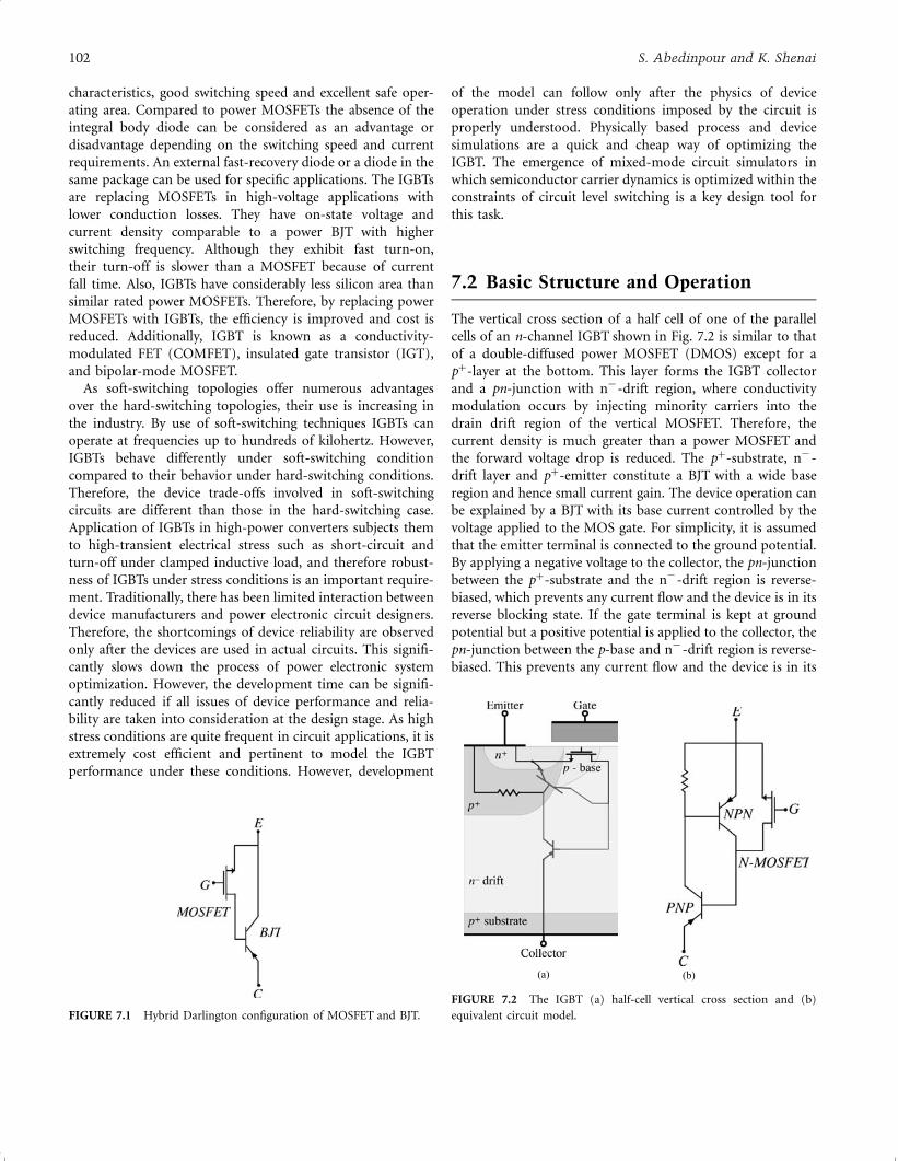
characteristics, good switching speed and excellent safe oper-
ating area. Compared to power MOSFETs the absence of the
integral body diode can be considered as an advantage or
disadvantage depending on the switching speed and current
requirements. An external fast-recovery diode or a diode in the
same package can be used for specific applications. The IGBTs
are replacing MOSFETs in high-voltage applications with
lower conduction losses. They have on-state voltage and
current density comparable to a power BJT with higher
switching frequency. Although they exhibit fast turn-on,
their turn-off is slower than a MOSFET because of current
fall time. Also, IGBTs have considerably less silicon area than
similar rated power MOSFETs. Therefore, by replacing power
MOSFETs with IGBTs, the efficiency is improved and cost is
reduced. Additionally, IGBT is known as a conductivity-
modulated FET (COMFET), insulated gate transistor (IGT),
and bipolar-mode MOSFET.
As soft-switching topologies offer numerous advantages
over the hard-switching topologies, their use is increasing in
the industry. By use of soft-switching techniques IGBTs can
operate at frequencies up to hundreds of kilohertz. However,
IGBTs behave differently under soft-switching condition
compared to their behavior under hard-switching conditions.
Therefore, the device trade-offs involved in soft-switching
circuits are different than those in the hard-switching case.
Application of IGBTs in high-power converters subjects them
to high-transient electrical stress such as short-circuit and
turn-off under clamped inductive load, and therefore robust-
ness of IGBTs under stress conditions is an important require-
ment. Traditionally, there has been limited interaction between
device manufacturers and power electronic circuit designers.
Therefore, the shortcomings of device reliability are observed
only after the devices are used in actual circuits. This signifi-
cantly slows down the process of power electronic system
optimization. However, the development time can be signifi-
cantly reduced if all issues of device performance and relia-
bility are taken into consideration at the design stage. As high
stress conditions are quite frequent in circuit applications, it is
extremely cost efficient and pertinent to model the IGBT
performance under these conditions. However, development
of the model can follow only after the physics of device
operation under stress conditions imposed by the circuit is
properly understood. Physically based process and device
simulations are a quick and cheap way of optimizing the
IGBT. The emergence of mixed-mode circuit simulators in
which semiconductor carrier dynamics is optimized within the
constraints of circuit level switching is a key design tool for
this task.
7.2 Basic Structure and Operation
The vertical cross section of a half cell of one of the parallel
cells of an n-channel IGBT shown in Fig. 7.2 is similar to that
of a double-diffused power MOSFET (DMOS) except for a
pþ-layer at the bottom. This layer forms the IGBT collector
and a pn-junction with nÿ-drift region, where conductivity
modulation occurs by injecting minority carriers into the
drain drift region of the vertical MOSFET. Therefore, the
current density is much greater than a power MOSFET and
the forward voltage drop is reduced. The pþ-substrate, nÿ-
drift layer and pþ-emitter constitute a BJT with a wide base
region and hence small current gain. The device operation can
be explained by a BJT with its base current controlled by the
voltage applied to the MOS gate. For simplicity, it is assumed
that the emitter terminal is connected to the ground potential.
By applying a negative voltage to the collector, the pn-junction
between the pþ-substrate and the nÿ-drift region is reverse-
biased, which prevents any current flow and the device is in its
reverse blocking state. If the gate terminal is kept at ground
potential but a positive potential is applied to the collector, the
pn-junction between the p-base and nÿ-drift region is reverse-
biased. This prevents any current flow and the device is in its
FIGURE 7.1 Hybrid Darlington configuration of MOSFET and BJT.
(a) (b)
FIGURE 7.2 The IGBT (a) half-cell vertical cross section and (b)
equivalent circuit model.
102 S. Abedinpour and K. Shenai
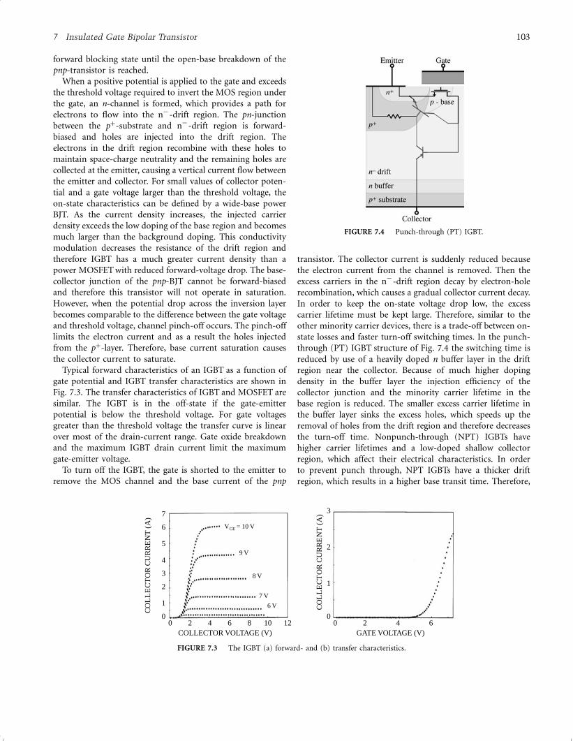
forward blocking state until the open-base breakdown of the
pnp-transistor is reached.
When a positive potential is applied to the gate and exceeds
the threshold voltage required to invert the MOS region under
the gate, an n-channel is formed, which provides a path for
electrons to flow into the nÿ-drift region. The pn-junction
between the pþ-substrate and nÿ-drift region is forward-
biased and holes are injected into the drift region. The
electrons in the drift region recombine with these holes to
maintain space-charge neutrality and the remaining holes are
collected at the emitter, causing a vertical current flow between
the emitter and collector. For small values of collector poten-
tial and a gate voltage larger than the threshold voltage, the
on-state characteristics can be defined by a wide-base power
BJT. As the current density increases, the injected carrier
density exceeds the low doping of the base region and becomes
much larger than the background doping. This conductivity
modulation decreases the resistance of the drift region and
therefore IGBT has a much greater current density than a
power MOSFET with reduced forward-voltage drop. The base-
collector junction of the pnp-BJT cannot be forward-biased
and therefore this transistor will not operate in saturation.
However, when the potential drop across the inversion layer
becomes comparable to the difference between the gate voltage
and threshold voltage, channel pinch-off occurs. The pinch-off
limits the electron current and as a result the holes injected
from the pþ-layer. Therefore, base current saturation causes
the collector current to saturate.
Typical forward characteristics of an IGBT as a function of
gate potential and IGBT transfer characteristics are shown in
Fig. 7.3. The transfer characteristics of IGBT and MOSFET are
similar. The IGBT is in the off-state if the gate-emitter
potential is below the threshold voltage. For gate voltages
greater than the threshold voltage the transfer curve is linear
over most of the drain-current range. Gate oxide breakdown
and the maximum IGBT drain current limit the maximum
gate-emitter voltage.
To turn off the IGBT, the gate is shorted to the emitter to
remove the MOS channel and the base current of the pnp
transistor. The collector current is suddenly reduced because
the electron current from the channel is removed. Then the
excess carriers in the nÿ-drift region decay by electron-hole
recombination, which causes a gradual collector current decay.
In order to keep the on-state voltage drop low, the excess
carrier lifetime must be kept large. Therefore, similar to the
other minority carrier devices, there is a trade-off between on-
state losses and faster turn-off switching times. In the punch-
through (PT) IGBT structure of Fig. 7.4 the switching time is
reduced by use of a heavily doped n buffer layer in the drift
region near the collector. Because of much higher doping
density in the buffer layer the injection efficiency of the
collector junction and the minority carrier lifetime in the
base region is reduced. The smaller excess carrier lifetime in
the buffer layer sinks the excess holes, which speeds up the
removal of holes from the drift region and therefore decreases
the turn-off time. Nonpunch-through (NPT) IGBTs have
higher carrier lifetimes and a low-doped shallow collector
region, which affect their electrical characteristics. In order
to prevent punch through, NPT IGBTs have a thicker drift
region, which results in a higher base transit time. Therefore,
CO
LL
EC
TO
RC
UR
RE
NT
(A)
1
2
3
420
0 6GATE VOLTAGE (V)
CO
LL
EC
TO
RC
UR
RE
NT
(A)
00 2 4 6 8 10 12
1
2
3
4
5
6
7
VGE = 10 V
9 V
8 V
7 V
6 V
COLLECTOR VOLTAGE (V)
FIGURE 7.3 The IGBT (a) forward- and (b) transfer characteristics.
FIGURE 7.4 Punch-through (PT) IGBT.
7 Insulated Gate Bipolar Transistor 103
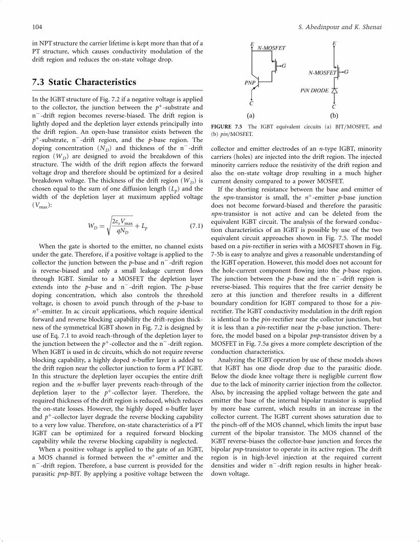
in NPT structure the carrier lifetime is kept more than that of a
PT structure, which causes conductivity modulation of the
drift region and reduces the on-state voltage drop.
7.3 Static Characteristics
In the IGBT structure of Fig. 7.2 if a negative voltage is applied
to the collector, the junction between the pþ-substrate and
nÿ-drift region becomes reverse-biased. The drift region is
lightly doped and the depletion layer extends principally into
the drift region. An open-base transistor exists between the
pþ-substrate, nÿ-drift region, and the p-base region. The
doping concentration (N D) and thickness of the nÿ-drift
region (W D) are designed to avoid the breakdown of this
structure. The width of the drift region affects the forward
voltage drop and therefore should be optimized for a desired
breakdown voltage. The thickness of the drift region (W D) is
chosen equal to the sum of one diffusion length (Lp) and the
width of the depletion layer at maximum applied voltage
(Vmax):
WD ¼
���������������2esVmax
qND
sþ Lp ð7:1Þ
When the gate is shorted to the emitter, no channel exists
under the gate. Therefore, if a positive voltage is applied to the
collector the junction between the p-base and nÿ-drift region
is reverse-biased and only a small leakage current flows
through IGBT. Similar to a MOSFET the depletion layer
extends into the p-base and nÿ-drift region. The p-base
doping concentration, which also controls the threshold
voltage, is chosen to avoid punch through of the p-base to
nþ-emitter. In ac circuit applications, which require identical
forward and reverse blocking capability the drift-region thick-
ness of the symmetrical IGBT shown in Fig. 7.2 is designed by
use of Eq. 7.1 to avoid reach-through of the depletion layer to
the junction between the pþ-collector and the nÿ-drift region.
When IGBT is used in dc circuits, which do not require reverse
blocking capability, a highly doped n-buffer layer is added to
the drift region near the collector junction to form a PT IGBT.
In this structure the depletion layer occupies the entire drift
region and the n-buffer layer prevents reach-through of the
depletion layer to the pþ-collector layer. Therefore, the
required thickness of the drift region is reduced, which reduces
the on-state losses. However, the highly doped n-buffer layer
and pþ-collector layer degrade the reverse blocking capability
to a very low value. Therefore, on-state characteristics of a PT
IGBT can be optimized for a required forward blocking
capability while the reverse blocking capability is neglected.
When a positive voltage is applied to the gate of an IGBT,
a MOS channel is formed between the nþ-emitter and the
nÿ-drift region. Therefore, a base current is provided for the
parasitic pnp-BJT. By applying a positive voltage between the
collector and emitter electrodes of an n-type IGBT, minority
carriers (holes) are injected into the drift region. The injected
minority carriers reduce the resistivity of the drift region and
also the on-state voltage drop resulting in a much higher
current density compared to a power MOSFET.
If the shorting resistance between the base and emitter of
the npn-transistor is small, the nþ-emitter p-base junction
does not become forward-biased and therefore the parasitic
npn-transistor is not active and can be deleted from the
equivalent IGBT circuit. The analysis of the forward conduc-
tion characteristics of an IGBT is possible by use of the two
equivalent circuit approaches shown in Fig. 7.5. The model
based on a pin-rectifier in series with a MOSFET shown in Fig.
7-5b is easy to analyze and gives a reasonable understanding of
the IGBT operation. However, this model does not account for
the hole-current component flowing into the p-base region.
The junction between the p-base and the nÿ-drift region is
reverse-biased. This requires that the free carrier density be
zero at this junction and therefore results in a different
boundary condition for IGBT compared to those for a pin-
rectifier. The IGBT conductivity modulation in the drift region
is identical to the pin-rectifier near the collector junction, but
it is less than a pin-rectifier near the p-base junction. There-
fore, the model based on a bipolar pnp-transistor driven by a
MOSFET in Fig. 7.5a gives a more complete description of the
conduction characteristics.
Analyzing the IGBT operation by use of these models shows
that IGBT has one diode drop due to the parasitic diode.
Below the diode knee voltage there is negligible current flow
due to the lack of minority carrier injection from the collector.
Also, by increasing the applied voltage between the gate and
emitter the base of the internal bipolar transistor is supplied
by more base current, which results in an increase in the
collector current. The IGBT current shows saturation due to
the pinch-off of the MOS channel, which limits the input base
current of the bipolar transistor. The MOS channel of the
IGBT reverse-biases the collector-base junction and forces the
bipolar pnp-transistor to operate in its active region. The drift
region is in high-level injection at the required current
densities and wider nÿ-drift region results in higher break-
down voltage.
(b)(a)
FIGURE 7.5 The IGBT equivalent circuits (a) BJT=MOSFET, and
(b) pin=MOSFET.
104 S. Abedinpour and K. Shenai
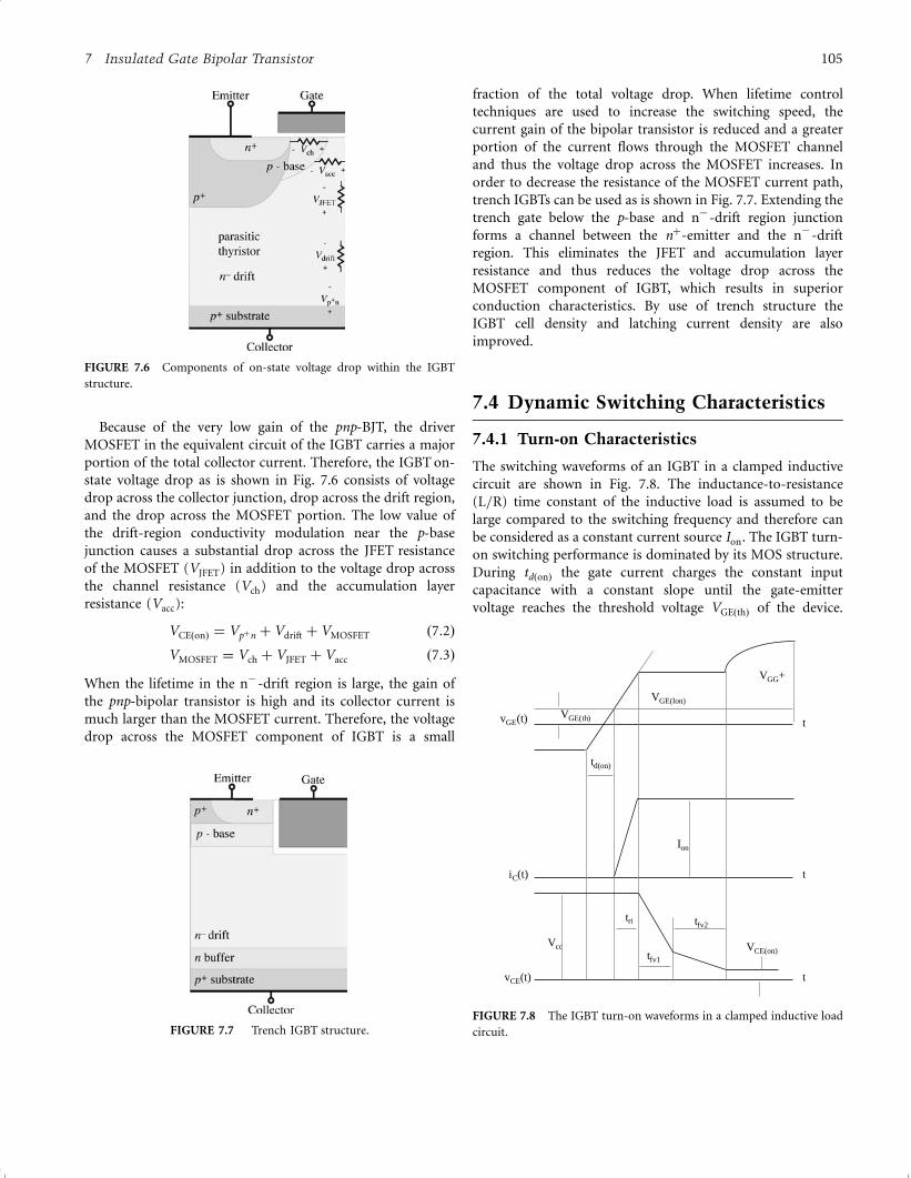
Because of the very low gain of the pnp-BJT, the driver
MOSFET in the equivalent circuit of the IGBT carries a major
portion of the total collector current. Therefore, the IGBT on-
state voltage drop as is shown in Fig. 7.6 consists of voltage
drop across the collector junction, drop across the drift region,
and the drop across the MOSFET portion. The low value of
the drift-region conductivity modulation near the p-base
junction causes a substantial drop across the JFET resistance
of the MOSFET (VJFET) in addition to the voltage drop across
the channel resistance (Vch) and the accumulation layer
resistance (Vacc):
VCEðonÞ ¼ Vpþn þ Vdrift þ VMOSFET ð7:2Þ
VMOSFET ¼ Vch þ VJFET þ Vacc ð7:3Þ
When the lifetime in the nÿ-drift region is large, the gain of
the pnp-bipolar transistor is high and its collector current is
much larger than the MOSFET current. Therefore, the voltage
drop across the MOSFET component of IGBT is a small
fraction of the total voltage drop. When lifetime control
techniques are used to increase the switching speed, the
current gain of the bipolar transistor is reduced and a greater
portion of the current flows through the MOSFET channel
and thus the voltage drop across the MOSFET increases. In
order to decrease the resistance of the MOSFET current path,
trench IGBTs can be used as is shown in Fig. 7.7. Extending the
trench gate below the p-base and nÿ-drift region junction
forms a channel between the nþ-emitter and the nÿ-drift
region. This eliminates the JFET and accumulation layer
resistance and thus reduces the voltage drop across the
MOSFET component of IGBT, which results in superior
conduction characteristics. By use of trench structure the
IGBT cell density and latching current density are also
improved.
7.4 Dynamic Switching Characteristics
7.4.1 Turn-on Characteristics
The switching waveforms of an IGBT in a clamped inductive
circuit are shown in Fig. 7.8. The inductance-to-resistance
(L=R) time constant of the inductive load is assumed to be
large compared to the switching frequency and therefore can
be considered as a constant current source Ion. The IGBT turn-
on switching performance is dominated by its MOS structure.
During tdðonÞ the gate current charges the constant input
capacitance with a constant slope until the gate-emitter
voltage reaches the threshold voltage VGEðthÞ of the device.
FIGURE 7.6 Components of on-state voltage drop within the IGBT
structure.
FIGURE 7.7 Trench IGBT structure.
VGE(th)
VGG+
t
t
t
Ion
td(on)
tri
Vcc
vCE(t)
iC(t)
vGE(t)
tfv1
tfv2
VCE(on)
VGE(Ion)
FIGURE 7.8 The IGBT turn-on waveforms in a clamped inductive load
circuit.
7 Insulated Gate Bipolar Transistor 105
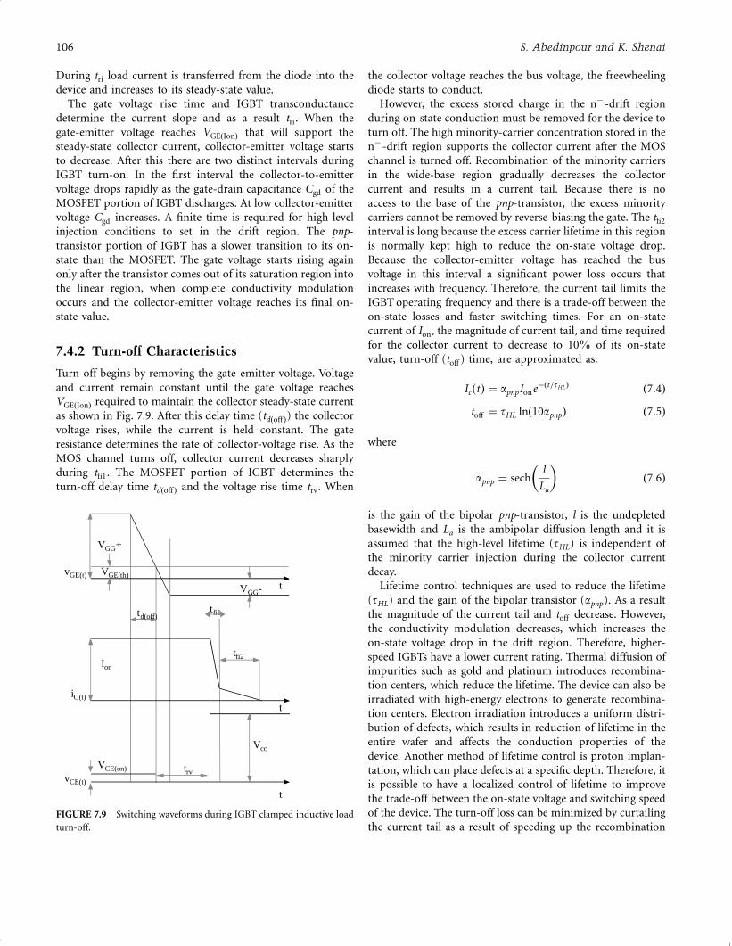
During tri load current is transferred from the diode into the
device and increases to its steady-state value.
The gate voltage rise time and IGBT transconductance
determine the current slope and as a result tri. When the
gate-emitter voltage reaches VGEðIonÞ that will support the
steady-state collector current, collector-emitter voltage starts
to decrease. After this there are two distinct intervals during
IGBT turn-on. In the first interval the collector-to-emitter
voltage drops rapidly as the gate-drain capacitance Cgd of the
MOSFET portion of IGBT discharges. At low collector-emitter
voltage Cgd increases. A finite time is required for high-level
injection conditions to set in the drift region. The pnp-
transistor portion of IGBT has a slower transition to its on-
state than the MOSFET. The gate voltage starts rising again
only after the transistor comes out of its saturation region into
the linear region, when complete conductivity modulation
occurs and the collector-emitter voltage reaches its final on-
state value.
7.4.2 Turn-off Characteristics
Turn-off begins by removing the gate-emitter voltage. Voltage
and current remain constant until the gate voltage reaches
VGEðIonÞ required to maintain the collector steady-state current
as shown in Fig. 7.9. After this delay time (tdðoff Þ) the collector
voltage rises, while the current is held constant. The gate
resistance determines the rate of collector-voltage rise. As the
MOS channel turns off, collector current decreases sharply
during tfi1. The MOSFET portion of IGBT determines the
turn-off delay time tdðoff Þ and the voltage rise time trv. When
the collector voltage reaches the bus voltage, the freewheeling
diode starts to conduct.
However, the excess stored charge in the nÿ-drift region
during on-state conduction must be removed for the device to
turn off. The high minority-carrier concentration stored in the
nÿ-drift region supports the collector current after the MOS
channel is turned off. Recombination of the minority carriers
in the wide-base region gradually decreases the collector
current and results in a current tail. Because there is no
access to the base of the pnp-transistor, the excess minority
carriers cannot be removed by reverse-biasing the gate. The tfi2
interval is long because the excess carrier lifetime in this region
is normally kept high to reduce the on-state voltage drop.
Because the collector-emitter voltage has reached the bus
voltage in this interval a significant power loss occurs that
increases with frequency. Therefore, the current tail limits the
IGBT operating frequency and there is a trade-off between the
on-state losses and faster switching times. For an on-state
current of Ion, the magnitude of current tail, and time required
for the collector current to decrease to 10% of its on-state
value, turn-off (toff ) time, are approximated as:
IcðtÞ ¼ apnpIoneÿðt=tHLÞ ð7:4Þ
toff ¼ tHL lnð10apnpÞ ð7:5Þ
where
apnp ¼ sechl
La
� �ð7:6Þ
is the gain of the bipolar pnp-transistor, l is the undepleted
basewidth and La is the ambipolar diffusion length and it is
assumed that the high-level lifetime (tHL) is independent of
the minority carrier injection during the collector current
decay.
Lifetime control techniques are used to reduce the lifetime
(tHL) and the gain of the bipolar transistor (apnp). As a result
the magnitude of the current tail and toff decrease. However,
the conductivity modulation decreases, which increases the
on-state voltage drop in the drift region. Therefore, higher-
speed IGBTs have a lower current rating. Thermal diffusion of
impurities such as gold and platinum introduces recombina-
tion centers, which reduce the lifetime. The device can also be
irradiated with high-energy electrons to generate recombina-
tion centers. Electron irradiation introduces a uniform distri-
bution of defects, which results in reduction of lifetime in the
entire wafer and affects the conduction properties of the
device. Another method of lifetime control is proton implan-
tation, which can place defects at a specific depth. Therefore, it
is possible to have a localized control of lifetime to improve
the trade-off between the on-state voltage and switching speed
of the device. The turn-off loss can be minimized by curtailing
the current tail as a result of speeding up the recombination
VGE(th)
VGG+
t
t
t
Ion
td(off)
trv
Vcc
vCE(t)
iC(t)
vGE(t)
VCE(on)
VGG-
tfi2
tfi1
FIGURE 7.9 Switching waveforms during IGBT clamped inductive load
turn-off.
106 S. Abedinpour and K. Shenai
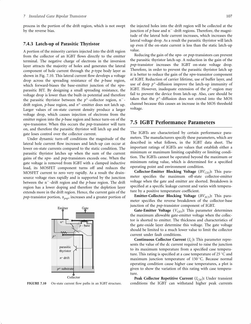
process in the portion of the drift region, which is not swept
by the reverse bias.
7.4.3 Latch-up of Parasitic Thyristor
A portion of the minority carriers injected into the drift region
from the collector of an IGBT flows directly to the emitter
terminal. The negative charge of electrons in the inversion
layer attracts the majority of holes and generates the lateral
component of hole current through the p-type body layer as
shown in Fig. 7.10. This lateral current flow develops a voltage
drop across the spreading resistance of the p-base region,
which forward-biases the base-emitter junction of the npn-
parasitic BJT. By designing a small spreading resistance, the
voltage drop is lower than the built-in potential and therefore
the parasitic thyristor between the pþ-collector region, nÿ-
drift region, p-base region, and nþ-emitter does not latch up.
Larger values of on-state current density produce a larger
voltage drop, which causes injection of electrons from the
emitter region into the p-base region and hence turn-on of the
npn-transistor. When this occurs the pnp-transistor will turn
on, and therefore the parasitic thyristor will latch up and the
gate loses control over the collector current.
Under dynamic turn-off conditions the magnitude of the
lateral hole current flow increases and latch-up can occur at
lower on-state currents compared to the static condition. The
parasitic thyristor latches up when the sum of the current
gains of the npn- and pnp-transistors exceeds one. When the
gate voltage is removed from IGBT with a clamped inductive
load, its MOSFET component turns off and reduces the
MOSFET current to zero very rapidly. As a result the drain-
source voltage rises rapidly and is supported by the junction
between the nÿ-drift region and the p-base region. The drift
region has a lower doping and therefore the depletion layer
extends more in the drift region. Hence, the current gain of the
pnp-transistor portion, apnp, increases and a greater portion of
the injected holes into the drift region will be collected at the
junction of p-base and nÿ-drift regions. Therefore, the magni-
tude of the lateral hole current increases, which increases the
lateral voltage drop. As a result the parasitic thyristor will latch
up even if the on-state current is less than the static latch-up
value.
Reducing the gain of the npn- or pnp-transistors can prevent
the parasitic thyristor latch-up. A reduction in the gain of the
pnp-transistor increases the IGBT on-state voltage drop.
Therefore, in order to prevent the parasitic thyristor latch up
it is better to reduce the gain of the npn-transistor component
of IGBT. Reduction of carrier lifetime, use of buffer layer, and
use of deep pþ-diffusion improve the latch-up immunity of
IGBT. However, inadequate extension of the pþ-region may
fail to prevent the device from latch-up. Also, care should be
taken that the pþ-diffusion does not extend into the MOS
channel because this causes an increase in the MOS threshold
voltage.
7.5 IGBT Performance Parameters
The IGBTs are characterized by certain performance para-
meters. The manufacturers specify these parameters, which are
described in what follows, in the IGBT data sheet. The
important ratings of IGBTs are values that establish either a
minimum or maximum limiting capability or limiting condi-
tion. The IGBTs cannot be operated beyond the maximum or
minimum rating value, which is determined for a specified
operating point and environment condition.
Collector-Emitter Blocking Voltage (BVCES): This para-
meter specifies the maximum off-state collector-emitter
voltage when the gate and emitter are shorted. Breakdown is
specified at a specific leakage current and varies with tempera-
ture by a positive temperature coefficient.
Emitter-Collector Blocking Voltage (BVECS): This para-
meter specifies the reverse breakdown of the collector-base
junction of the pnp-transistor component of IGBT.
Gate-Emitter Voltage (VGES): This parameter determines
the maximum allowable gate-emitter voltage when the collec-
tor is shorted to emitter. The thickness and characteristics of
the gate-oxide layer determine this voltage. The gate voltage
should be limited to a much lower value to limit the collector
current under fault conditions.
Continuous Collector Current (IC ): This parameter repre-
sents the value of the dc current required to raise the junction
to its maximum temperature from a specified case tempera-
ture. This rating is specified at a case temperature of 25 �C and
maximum junction temperature of 150 �C. Because normal
operating condition cause higher case temperatures, a plot is
given to show the variation of this rating with case tempera-
ture.
Peak Collector Repetitive Current (ICM ): Under transient
conditions the IGBT can withstand higher peak currentsFIGURE 7.10 On-state current flow paths in an IGBT structure.
7 Insulated Gate Bipolar Transistor 107
compared to its maximum continuous current, which is
described by this parameter.
Maximum Power Dissipation (PD): This parameter repre-
sents the power dissipation required to raise the junction
temperature to its maximum value of 150 �C, at a case
temperature of 25 �C. Normally a plot is provided to show
the variation of this rating with temperature.
Junction Temperature (Tj): Specifies the allowable range of
the IGBT junction temperature during its operation.
Clamped Inductive Load Current (ILM ): This parameter
specifies the maximum repetitive current that IGBT can turn
off under a clamped inductive load. During IGBT turn-on, the
reverse recovery current of the freewheeling diode in parallel
with the inductive load increases the IGBT turn-on switching
loss.
Collector-Emitter Leakage Current (ICES): This parameter
determines the leakage current at the rated voltage and specific
temperature when the gate is shorted to emitter.
Gate-Emitter Threshold Voltage (VGEðthÞ): This parameter
specifies the gate-emitter voltage range, where the IGBT is
turned on to conduct the collector current. The threshold
voltage has a negative temperature coefficient. Threshold
voltage increases linearly with gate-oxide thickness and as
the square root of the p-base doping concentration. Fixed
surface charge at the oxide-silicon interface and mobile ions in
the oxide shift the threshold voltage.
Collector-Emitter Saturation Voltage (VCEðSAT Þ): This
parameter specifies the collector-emitter forward voltage
drop and is a function of collector current, gate voltage, and
temperature. Reducing the resistance of the MOSFET channel
and JFET region, and increasing the gain of the pnp-bipolar
transistor can minimize the on-state voltage drop. The voltage
drop across the MOSFET component of IGBT, which provides
the base current of the pnp-transistor is reduced by a larger
channel width, shorter channel length, lower threshold
voltage, and wider gate length. Higher minority carrier life-
time and a thin n-epi region cause high carrier injection and
reduce the voltage drop in the drift region.
Forward Transconductance (gFE): Forward transconduc-
tance is measured with a small variation on the gate voltage,
which linearly increases the IGBT collector current to its rated
current at 100 �C. The transconductance of an IGBT is reduced
at currents much higher than its thermal-handling capability.
Therefore, unlike the bipolar transistors, the current-handling
capability of IGBTs is limited by thermal consideration and
not by its gain. At higher temperatures, the transconductance
starts to decrease at lower collector currents. Therefore these
features of transconductance protect the IGBT under short-
circuit operation.
Total Gate Charge (QG): This parameter helps to design a
suitably sized gate-drive circuit and approximately calculate its
losses. Because of the minority-carrier behavior of the device,
the switching times cannot be approximately calculated by use
of gate-charge value. This parameter varies as a function of the
gate-emitter voltage.
Turn-on Delay Time (td): This is defined as the time
between 10% of gate voltage to 10% of the final collector
current.
Rise Time (t r ): This is the time required for the collector
current to increase to 90% of its final value from 10% of its
final value.
Turn-off Delay Time (tdðoff Þ): This is the time between 90%of gate voltage to 10% of final collector voltage.
Fall Time (tf ): This is the time required for the collector
current to drop from 90% of its initial value to 10% of its
initial value.
Input Capacitance (Cies): The measured gate-emitter capa-
citance when collector is shorted to emitter. The input
capacitance is the sum of the gate-emitter and the Miller
capacitance. The gate-emitter capacitance is much larger than
the Miller capacitance.
Output Capacitance (Coes): The capacitance between collec-
tor and emitter when the gate is shorted to the emitter, which
has the typical pn-junction voltage dependency.
Reverse Transfer Capacitance (Cres): The Miller capacitance
between gate and collector, which has a complex voltage
dependency.
Safe Operating Area (SOA): The safe operating area deter-
mines the current and voltage boundary within which the
IGBT can be operated without destructive failure. At low
currents the maximum IGBT voltage is limited by the open-
base transistor breakdown. The parasitic thyristor latch-up
limits the maximum collector current at low voltages. While
IGBTs immune to static latch-up may be vulnerable to
dynamic latch-up, operation in short-circuit and inductive
load switching are conditions that would subject an IGBT to a
combined voltage and current stress. A forward-biased safe
operating area (FBSOA) is defined during the turn-on tran-
sient of the inductive load switching when both electron and
hole current flow in the IGBT in the presence of high voltage
across the device. The reverse-biased safe operating area
(RBSOA) is defined during the turn-off transient, where
only hole current flows in the IGBT with high voltage across it.
If the time duration of simultaneous high voltage and high
current is long enough, the IGBT failure will occur because of
thermal breakdown. However, if this time duration is short,
the temperature rise due to power dissipation will not be
enough to cause thermal breakdown. Under this condition the
avalanche breakdown occurs at voltage levels lower than the
breakdown voltage of the device. Compared to the steady-state
forward blocking condition the much larger charge in the drift
region causes a higher electric field and narrower depletion
region at the p-base and nÿ-drift junction. Under RBSOA
conditions there is no electron in the space-charge region and
therefore there is a larger increase in electric field than the
FBSOA condition.
108 S. Abedinpour and K. Shenai
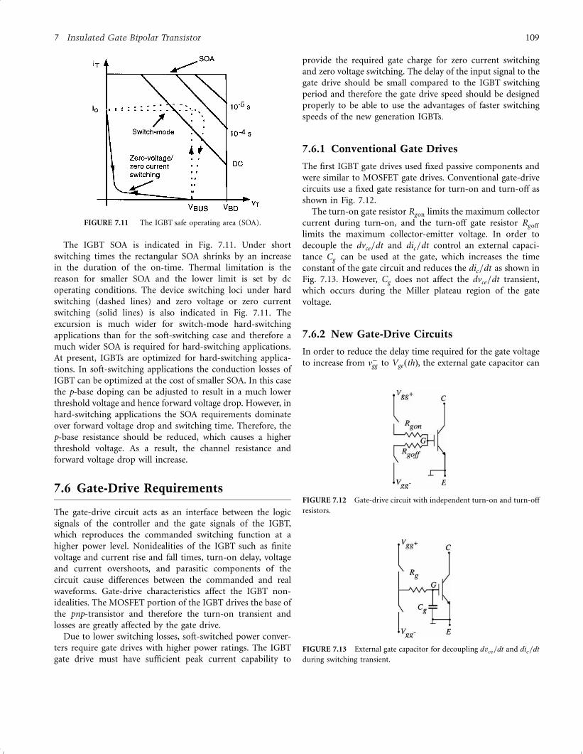
The IGBT SOA is indicated in Fig. 7.11. Under short
switching times the rectangular SOA shrinks by an increase
in the duration of the on-time. Thermal limitation is the
reason for smaller SOA and the lower limit is set by dc
operating conditions. The device switching loci under hard
switching (dashed lines) and zero voltage or zero current
switching (solid lines) is also indicated in Fig. 7.11. The
excursion is much wider for switch-mode hard-switching
applications than for the soft-switching case and therefore a
much wider SOA is required for hard-switching applications.
At present, IGBTs are optimized for hard-switching applica-
tions. In soft-switching applications the conduction losses of
IGBT can be optimized at the cost of smaller SOA. In this case
the p-base doping can be adjusted to result in a much lower
threshold voltage and hence forward voltage drop. However, in
hard-switching applications the SOA requirements dominate
over forward voltage drop and switching time. Therefore, the
p-base resistance should be reduced, which causes a higher
threshold voltage. As a result, the channel resistance and
forward voltage drop will increase.
7.6 Gate-Drive Requirements
The gate-drive circuit acts as an interface between the logic
signals of the controller and the gate signals of the IGBT,
which reproduces the commanded switching function at a
higher power level. Nonidealities of the IGBT such as finite
voltage and current rise and fall times, turn-on delay, voltage
and current overshoots, and parasitic components of the
circuit cause differences between the commanded and real
waveforms. Gate-drive characteristics affect the IGBT non-
idealities. The MOSFET portion of the IGBT drives the base of
the pnp-transistor and therefore the turn-on transient and
losses are greatly affected by the gate drive.
Due to lower switching losses, soft-switched power conver-
ters require gate drives with higher power ratings. The IGBT
gate drive must have sufficient peak current capability to
provide the required gate charge for zero current switching
and zero voltage switching. The delay of the input signal to the
gate drive should be small compared to the IGBT switching
period and therefore the gate drive speed should be designed
properly to be able to use the advantages of faster switching
speeds of the new generation IGBTs.
7.6.1 Conventional Gate Drives
The first IGBT gate drives used fixed passive components and
were similar to MOSFET gate drives. Conventional gate-drive
circuits use a fixed gate resistance for turn-on and turn-off as
shown in Fig. 7.12.
The turn-on gate resistor Rgon limits the maximum collector
current during turn-on, and the turn-off gate resistor Rgoff
limits the maximum collector-emitter voltage. In order to
decouple the dvce=dt and dic=dt control an external capaci-
tance Cg can be used at the gate, which increases the time
constant of the gate circuit and reduces the dic=dt as shown in
Fig. 7.13. However, Cg does not affect the dvce=dt transient,
which occurs during the Miller plateau region of the gate
voltage.
7.6.2 New Gate-Drive Circuits
In order to reduce the delay time required for the gate voltage
to increase from vÿgg to VgeðthÞ, the external gate capacitor can
FIGURE 7.11 The IGBT safe operating area (SOA).
FIGURE 7.12 Gate-drive circuit with independent turn-on and turn-off
resistors.
FIGURE 7.13 External gate capacitor for decoupling dvce=dt and dic=dt
during switching transient.
7 Insulated Gate Bipolar Transistor 109
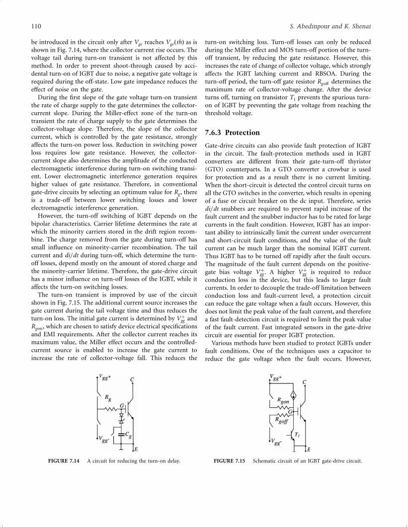
be introduced in the circuit only after Vge reaches VgeðthÞ as is
shown in Fig. 7.14, where the collector current rise occurs. The
voltage tail during turn-on transient is not affected by this
method. In order to prevent shoot-through caused by acci-
dental turn-on of IGBT due to noise, a negative gate voltage is
required during the off-state. Low gate impedance reduces the
effect of noise on the gate.
During the first slope of the gate voltage turn-on transient
the rate of charge supply to the gate determines the collector-
current slope. During the Miller-effect zone of the turn-on
transient the rate of charge supply to the gate determines the
collector-voltage slope. Therefore, the slope of the collector
current, which is controlled by the gate resistance, strongly
affects the turn-on power loss. Reduction in switching power
loss requires low gate resistance. However, the collector-
current slope also determines the amplitude of the conducted
electromagnetic interference during turn-on switching transi-
ent. Lower electromagnetic interference generation requires
higher values of gate resistance. Therefore, in conventional
gate-drive circuits by selecting an optimum value for Rg, there
is a trade-off between lower switching losses and lower
electromagnetic interference generation.
However, the turn-off switching of IGBT depends on the
bipolar characteristics. Carrier lifetime determines the rate at
which the minority carriers stored in the drift region recom-
bine. The charge removed from the gate during turn-off has
small influence on minority-carrier recombination. The tail
current and di=dt during turn-off, which determine the turn-
off losses, depend mostly on the amount of stored charge and
the minority-carrier lifetime. Therefore, the gate-drive circuit
has a minor influence on turn-off losses of the IGBT, while it
affects the turn-on switching losses.
The turn-on transient is improved by use of the circuit
shown in Fig. 7.15. The additional current source increases the
gate current during the tail voltage time and thus reduces the
turn-on loss. The initial gate current is determined by Vþgg and
Rgon, which are chosen to satisfy device electrical specifications
and EMI requirements. After the collector current reaches its
maximum value, the Miller effect occurs and the controlled-
current source is enabled to increase the gate current to
increase the rate of collector-voltage fall. This reduces the
turn-on switching loss. Turn-off losses can only be reduced
during the Miller effect and MOS turn-off portion of the turn-
off transient, by reducing the gate resistance. However, this
increases the rate of change of collector voltage, which strongly
affects the IGBT latching current and RBSOA. During the
turn-off period, the turn-off gate resistor Rgoff determines the
maximum rate of collector-voltage change. After the device
turns off, turning on transistor T1 prevents the spurious turn-
on of IGBT by preventing the gate voltage from reaching the
threshold voltage.
7.6.3 Protection
Gate-drive circuits can also provide fault protection of IGBT
in the circuit. The fault-protection methods used in IGBT
converters are different from their gate-turn-off thyristor
(GTO) counterparts. In a GTO converter a crowbar is used
for protection and as a result there is no current limiting.
When the short-circuit is detected the control circuit turns on
all the GTO switches in the converter, which results in opening
of a fuse or circuit breaker on the dc input. Therefore, series
di=dt snubbers are required to prevent rapid increase of the
fault current and the snubber inductor has to be rated for large
currents in the fault condition. However, IGBT has an impor-
tant ability to intrinsically limit the current under overcurrent
and short-circuit fault conditions, and the value of the fault
current can be much larger than the nominal IGBT current.
Thus IGBT has to be turned off rapidly after the fault occurs.
The magnitude of the fault current depends on the positive-
gate bias voltage Vþgg . A higher Vþgg is required to reduce
conduction loss in the device, but this leads to larger fault
currents. In order to decouple the trade-off limitation between
conduction loss and fault-current level, a protection circuit
can reduce the gate voltage when a fault occurs. However, this
does not limit the peak value of the fault current, and therefore
a fast fault-detection circuit is required to limit the peak value
of the fault current. Fast integrated sensors in the gate-drive
circuit are essential for proper IGBT protection.
Various methods have been studied to protect IGBTs under
fault conditions. One of the techniques uses a capacitor to
reduce the gate voltage when the fault occurs. However,
FIGURE 7.14 A circuit for reducing the turn-on delay. FIGURE 7.15 Schematic circuit of an IGBT gate-drive circuit.
110 S. Abedinpour and K. Shenai
depending on the initial condition of the capacitor and its
value, the IGBT current may reduce to zero and then turn on
again. Another method is to softly turn off the IGBT after the
fault and to reduce the overvoltage due to dic=dt . Therefore,
the overvoltage on IGBT caused by the parasitic inductance is
limited while turning off large currents. The most common
method of IGBT protection is collector-voltage monitoring or
desaturation detection. The monitored parameter is the collec-
tor-emitter voltage, which makes fault detection easier
compared to measuring the device current. However, voltage
detection can be activated only after the complete turn on of
IGBT. If the fault current increases slowly due to large fault
inductance, the fault detection is difficult because the collec-
tor-emitter voltage will not change significantly. In order to
determine whether the current that is being turned off is
overcurrent or nominal current, the Miller voltage plateau
level can be used. This method can be used to initiate soft
turn-off and to reduce the overvoltage during overcurrents.
Special sense IGBTs have been introduced at low-power
levels with a sense terminal to provide a current signal
proportional to the IGBT collector current. A few active
device cells are used to mirror the current carried by the
other cells. Unfortunately, however, sense IGBTs are not
available at high-power levels and there are problems related
to the higher conduction losses in the sense device. The most
reliable method to detect an overcurrent fault condition is to
introduce a current sensor in series with the IGBT. The
additional current sensor makes the power circuit more
complex and may lead to parasitic bus inductance, which
results in higher overvoltages during turn off.
After the fault occurs the IGBT has to be safely turned off.
Due to large dic=dt during turn-off, the overvoltage can be
very large. Therefore, many techniques have been investigated
to obtain soft turn-off. The most common method is to use a
large turn-off gate resistor when the fault occurs. Another
method to reduce the turn-off overvoltage is to lower the
fault-current level by reducing the gate voltage before initiat-
ing the turn-off. A resistive voltage divider can be used to
reduce the gate voltage during fault turn-off. For example, the
gate-voltage reduction can be obtained by turning on simul-
taneously Rgoff and Rgon in the circuit of Fig. 7.12. Another
method is to switch a capacitor into the gate and rapidly
discharge the gate during the occurrence of a fault. To prevent
the capacitor from charging back up to the nominal on-state
gate voltage, a large capacitor should be used, which may cause
a rapid gate discharge. Also, a Zener diode can be used in the
gate to reduce the gate voltage after a fault occurs, but the slow
transient behavior of the Zener diode leads to large initial peak
fault current. The power dissipation during a fault determines
the time duration that the fault current can flow in the IGBT
without damaging it. Therefore, the IGBT fault-endurance
capability is improved by the use of fault-current limiting
circuits to reduce the power dissipation in the IGBT under
fault conditions.
7.7 Circuit Models
A high-quality IGBT model for circuit simulation is essential
for improving the efficiency and reliability in the design of
power electronic circuits. Conventional models for power
semiconductor devices simply described an abrupt or linear
switching behavior and a fixed resistance during the conduc-
tion state. Low switching frequencies of power circuits made it
possible to use these approximate models. However, moving
to higher switching frequencies to reduce the size of a power
electronic system requires high-quality power semiconductor
device models for circuit simulation.
The n-channel IGBT consists of a pnp-bipolar transistor
whose base current is provided by an n-channel MOSFET, as is
shown in Fig. 7.1. Therefore, the IGBT behavior is determined
by physics of the bipolar and MOSFET devices. Several effects
dominate the static and dynamic device characteristics. The
influence of these effects on a low-power semiconductor
device is negligible and therefore they cannot be described
by standard device models. The conventional circuit models
were developed to describe the behavior of low-power devices,
and therefore were not adequate to be modified for IGBT. The
reason is that the bipolar transistor and MOSFET in the IGBT
have a different behavior compared to their low-power coun-
terparts; they also have different structures.
The currently available models have different levels of
accuracy at the expense of speed. Circuit issues such as
switching losses and reliability are strongly dependent on the
device and require accurate device models. However, simpler
models are only adequate for system-oriented issues such as
the behavior of an electric motor driven by a pulsewidth
modulation (PWM) converter. Finite-element models have
high accuracy, but are slow and require internal device
structure details. Macromodels are fast but have low accuracy,
which depends on the operating point. Commercial circuit
simulators have introduced one-dimensional (1D) physics-
based models, which offer a compromise between the finite-
element models and macromodels. The Hefner model and the
Kraus model are such examples that have been implemented
in Saber and there has been some effort to implement them in
PSPICE. The Hefner model depends on the redistribution of
charge in the drift region during transients. The Kraus model
depends on the extraction of charge from the drift region by
the electric field and emitter back-injection.
The internal BJT of the IGBT has a wide base, which is
lightly doped to support the depletion region to have high
blocking voltages. The excess carrier lifetime in the base region
is low to have fast turn-off. However, low-power bipolar
transistors have high excess carrier lifetime in the base,
narrow base and high current gain. A finite base transit time
is required for a change in the injected base charge to change
the collector current. Therefore, quasi-static approximation
cannot be used at high speeds and the transport of carriers
7 Insulated Gate Bipolar Transistor 111
in the base should be described by ambipolar transport
theory.
7.7.1 Input and Output Characteristics
The bipolar and MOSFET components of a symmetric IGBT
are shown in Fig. 7.16. The components between the emitter
(e), base (b), and collector (c) terminals correspond to the
bipolar transistor and those between gate (g), source (s), and
drain (d) are associated with MOSFET. The combination of
the drain-source and gate-drain depletion capacitances is
identical to the base-collector depletion capacitance, and
therefore they are shown for the MOSFET components. The
gate-oxide capacitance of the source overlap (Coxs) and source
metallization capacitance (Cm) form the gate-source capaci-
tance (Cgs). When the MOSFET is in its linear region the gate-
oxide capacitance of the drain overlap (Coxd) forms the gate-
drain capacitance (Cgd). In the saturation region of MOSFET
the equivalent series connection of gate-drain overlap oxide
capacitance and the depletion capacitance of the gate-drain
overlap (Cgdj) forms the gate-drain Miller capacitance. The
gate-drain depletion width and the drain-source depletion
width are voltage dependent, which has the same effect on
the corresponding capacitances.
The most important capacitance in IGBT is the capacitance
between the input terminal (g) and output terminal (a),
because the switching characteristics are affected by this feed-
back.
Cga ¼dQg
dvga
¼ Cox
dvox
dvga
ð7:7Þ
Cox is determined by the oxide thickness and device area. The
accumulation, depletion, and inversion states below the gate
cause different states of charge and therefore different capaci-
tance values.
The stored charge in the lightly doped wide base of the
bipolar component of IGBT causes switching delays and
switching losses. The standard quasi-static charge description
is not adequate for IGBT because it assumes that the charge
distribution is a function of the IGBT terminal voltage.
However, the stored charge density (p(x,t)) changes with
time and position and therefore the ambipolar diffusion
equation must be used to describe the charge variation:
dPðx; tÞ
dt¼ ÿ
Pðx; tÞ
ta
þ Da
d2Pðx; tÞ
dx2ð7:8Þ
The slope of the charge-carrier distribution determines
the sum of electron and hole currents. The nonquasistatic
behavior of the stored charge in the base of the bipolar
component of IGBT results in the collector-emitter redistribu-
tion capacitance (Ccer ). This capacitance dominates the output
capacitance of IGBT during turn-off and describes the rate of
change of the base-collector depletion layer with the rate of
change of the base-collector voltage. However, the base-
collector displacement current is determined by the gate-
drain (Cgdj) and drain-source (Cdsj) capacitance of the
MOSFET component.
7.7.2 Implementing the IGBT Model into aCircuit Simulator
Usually a netlist is employed in a circuit simulator such as
Saber to describe an electrical circuit. Each component of the
circuit is defined by a model template with the component
terminal connection and the model parameters values. While
Saber libraries provide some standard component models, the
models can be generated by implementing the model equa-
tions in a defined Saber template. Electrical component
models of IGBT are defined by the current through each
component element as a function of component variables,
such as terminal and internal node voltages and explicitly
defined variables. The circuit simulator uses the Kirchhoff
current law to solve for electrical component variables such
that the total current into each node is equal to zero, while
satisfying the explicitly defined component variables needed to
describe the state of the device.
The IGBT circuit model is generated by defining the
currents between terminal nodes as a nonlinear function of
component variables and their rate of change. An IGBT circuit
model is shown in Fig. 7.17. Compared to Fig. 7.16 the bipolar
transistor is replaced by the two base and collector-current
sources. There is a distributed voltage drop due to diffusion
and drift in the base regions. The drift terms in the ambipolar
diffusion equation depend on base and collector currents.
Therefore, both of these currents generate the resistive voltage
drop Vae and Rb is placed at the emitter terminal in the IGBT
circuit model. The capacitance of the emitter-base junctionFIGURE 7.16 Symmetric IGBT half cell.
112 S. Abedinpour and K. Shenai
(Ceb) is implicitly defined by the emitter-base voltage as a
function of base charge; Iceb is the emitter-base capacitor
current that defines the rate of change of the base charge.
The current through the collector-emitter redistribution capa-
citance (Iccer ) is part of the collector current, which in contrast
to Icss depends on the rate of change of the base-emitter
voltage; Ibss is part of the base current that does not flow
through Ceb and does not depend on the rate of change of
base-collector voltage.
Impact ionization causes carrier multiplication in the high
electric field of the base-collector depletion region. This carrier
multiplication generates an additional base-collector current
component (Imult), which is proportional to Ic , Imos, and the
multiplication factor. The resulting Saber IGBT model should
be able to describe accurately the experimental results for the
range of static and dynamic conditions where IGBT operates.
Therefore, the model can be used to describe the steady-state
and dynamic characteristics under various circuit conditions.
The currently available models have different levels of
accuracy at the expense of speed. Circuit issues such as
switching losses and reliability are strongly dependent on the
device and require accurate device models. However, simpler
models are adequate for system-oriented issues such as the
behavior of an electric motor driven by a PWM converter.
Finite-element models have high accuracy, but are slow and
require internal device structure details. Macromodels are fast
but have low accuracy, which depends on the operating point.
Commercial circuit simulators have introduced 1D physics-
based models, which offer a compromise between the finite-
element models and macromodels.
7.8 Applications
Power electronics evolution is a result of the evolution of
power semiconductor devices. Applications of power electro-
nics are still expanding in industrial and utility systems. A
major challenge in designing power electronic systems is
simultaneous operation at high power and high switching
frequency. The advent of IGBTs has revolutionized power
electronics by extending the power and frequency boundary.
During the last decade the conduction and switching losses of
IGBTs have been reduced in the process of transition from the
first- to the third-generation IGBTs. The improved character-
istics of the IGBTs have resulted in higher switching speed and
lower energy losses. High-voltage IGBTs are expected to take
the place of high-voltage GTO thyristor converters in the near
future. To advance the performance beyond the third-genera-
tion IGBTs, the fourth-generation devices will require exploit-
ing fine-line lithographic technology and employing the
trench technology used to produce power MOSFETs with
very low on-state resistance. Intelligent IGBT or intelligent
power module (IPM) is an attractive power device integrated
with circuits to protect against overcurrent, overvoltage, and
overheating. The main application of IGBT is for use as a
switching component in inverter circuits, which are used in
both power supply and motor drive applications. The advan-
tages of using IGBT in these converters are simplicity and
modularity of the converter, simple gate drive, elimination of
snubber circuits due to the square SOA, lower switching loss,
improved protection characteristics in case of overcurrent and
short-circuit fault, galvanic isolation of the modules, and
simpler mechanical construction of the power converter.
These advantages have made the IGBT the preferred switching
device in the power range below 1 MW.
Power supply applications of IGBTs include uninterruptible
power supplies (UPS) as is shown in Fig. 7.18, constant-
voltage constant-frequency power supplies, induction heating
systems, switch mode power supplies, welders (Fig. 7.19),
cutters, traction power supplies, and medical equipment
(CT, X-ray). Low-noise operation, small size, low cost and
high accuracy are characteristics of the IGBT converters in
these applications. Examples of motor drive applications
include the variable-voltage variable-frequency inverter as is
GATE
ANODE
e
Rb
b
c
d
g
Ccer
Icss I bss
Imult
Cdsj
CgdCgs
CATHODE
Ceb
s
a
IcebI ccer
I mos
I c
xα
FIGURE 7.17 IGBT circuit model.
7 Insulated Gate Bipolar Transistor 113
shown in Fig. 7.20. The IGBTS have been introduced at high
voltage and current levels, which has enabled their use in high-
power converters utilized for medium-voltage motor drives.
The improved characteristics of the IGBTs have introduced
power converters in megawatt power applications such as
traction drives. One of the critical issues in realizing high-
power converters is the reliability of the power switches. The
devices used in these applications must be robust and capable
of withstanding faults long enough for a protection scheme to
be activated. The hard-switching voltage source power conver-
ter is the most commonly used topology. In this switch-mode
operation the switches are subjected to high switching stresses
and high-switching power loss that increase linearly with the
switching frequency of the pulsewidth modulation (PWM).
The resulting switching loci in the vt ÿ it plane is shown by
the dotted lines in Fig. 7.11. Because of simultaneous large
switch voltage and large switch current, the switch must be
capable of withstanding high switching stresses with a large
SOA. The requirement of being able to withstand large stresses
results in design compromises in other characteristics of the
power semiconductor device. Often forward voltage drop and
switching speed are sacrificed for enhanced short-circuit
capability. Process parameters of the IGBT such as threshold
voltage, carrier lifetime, and the device thickness can be varied
to obtain various combinations of SOA, on-state voltage, and
switching time. However, there is very little overlap in the
optimum combination for more than one performance para-
meter. Therefore, improved performance in one parameter is
achieved at the cost of other parameters.
In order to reduce the size, the weight, and the cost of
circuit components used in a power electronics converter very
high switching frequencies of the order of a few megahertz are
being contemplated. In order to be able to increase the
switching frequency, the problems of switch stresses, switching
losses and the EMI associated with switch-mode applications
need to be solved. Use of soft-switching converters reduces the
problems of high dv=dt and high di=dt by use of external
inductive and capacitive components to shape the switching
trajectory of the device. The device-switching loci resulting
from soft switching is shown in Fig. 7.11, where significant
reduction in switching stress can be noticed. The traditional
snubber circuits achieve this goal without the added control
complexity, but the power dissipation in these snubber circuits
can be large and limit the switching frequency of the converter.
Also, passive components significantly add to the size, weight,
and cost of the converter at high power levels. Soft switching
uses lossless resonant circuits, which solves the problem of
power loss in the snubber circuit, but increases the conduction
loss. Resonant transition circuits eliminate the problem of
high peak device stress in the soft-switched converters. The
main drawback of these circuits is the increased control
complexity required to obtain the resonant switching transi-
tion. The large number of circuit variables to be sensed in such
power converters can affect their reliability. With short-circuit
capability no longer being the primary concern, designers can
push the performance envelope for their circuits until the
device becomes the limiting factor once again.
The transient response of the conventional volts=hertz
induction motor drive is sluggish because both torque and
flux are functions of stator voltage and frequency. Use of
vector or field-oriented control methods makes the perfor-
mance of the induction motor drive almost identical to that of
a separately excited dc motor. Therefore, the transient
response is similar to a dc machine, where torque and flux
can be controlled in a decoupled manner. Vector-controlled
induction motors with shaft encoders or speed sensors have
been widely applied in combination with voltage-source PWM
inverters using IGBT modules. According to the specification
of the new products, vector-controlled induction motor drive
systems ranging from kilowatts to megawatts provide a broad
range of speed control, constant torque operation, and high
starting torque.
FIGURE 7.18 Constant-voltage, constant-frequency inverter (UPS).
FIGURE 7.19 IGBT welder.
FIGURE 7.20 Variable-voltage, variable-frequency inverter (PWM).
114 S. Abedinpour and K. Shenai
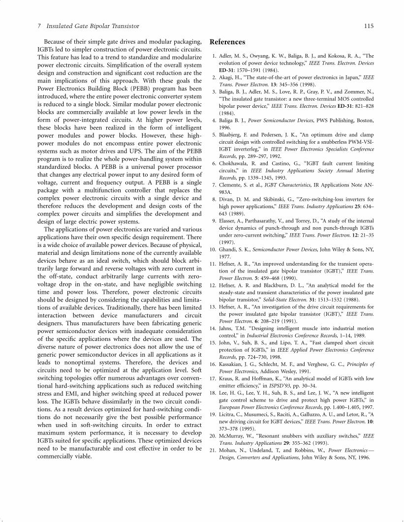
Because of their simple gate drives and modular packaging,
IGBTs led to simpler construction of power electronic circuits.
This feature has lead to a trend to standardize and modularize
power electronic circuits. Simplification of the overall system
design and construction and significant cost reduction are the
main implications of this approach. With these goals the
Power Electronics Building Block (PEBB) program has been
introduced, where the entire power electronic converter system
is reduced to a single block. Similar modular power electronic
blocks are commercially available at low power levels in the
form of power-integrated circuits. At higher power levels,
these blocks have been realized in the form of intelligent
power modules and power blocks. However, these high-
power modules do not encompass entire power electronic
systems such as motor drives and UPS. The aim of the PEBB
program is to realize the whole power-handling system within
standardized blocks. A PEBB is a universal power processor
that changes any electrical power input to any desired form of
voltage, current and frequency output. A PEBB is a single
package with a multifunction controller that replaces the
complex power electronic circuits with a single device and
therefore reduces the development and design costs of the
complex power circuits and simplifies the development and
design of large electric power systems.
The applications of power electronics are varied and various
applications have their own specific design requirement. There
is a wide choice of available power devices. Because of physical,
material and design limitations none of the currently available
devices behave as an ideal switch, which should block arbi-
trarily large forward and reverse voltages with zero current in
the off-state, conduct arbitrarily large currents with zero-
voltage drop in the on-state, and have negligible switching
time and power loss. Therefore, power electronic circuits
should be designed by considering the capabilities and limita-
tions of available devices. Traditionally, there has been limited
interaction between device manufacturers and circuit
designers. Thus manufacturers have been fabricating generic
power semiconductor devices with inadequate consideration
of the specific applications where the devices are used. The
diverse nature of power electronics does not allow the use of
generic power semiconductor devices in all applications as it
leads to nonoptimal systems. Therefore, the devices and
circuits need to be optimized at the application level. Soft
switching topologies offer numerous advantages over conven-
tional hard-switching applications such as reduced switching
stress and EMI, and higher switching speed at reduced power
loss. The IGBTs behave dissimilarly in the two circuit condi-
tions. As a result devices optimized for hard-switching condi-
tions do not necessarily give the best possible performance
when used in soft-switching circuits. In order to extract
maximum system performance, it is necessary to develop
IGBTs suited for specific applications. These optimized devices
need to be manufacturable and cost effective in order to be
commercially viable.
References
1. Adler, M. S., Owyang, K. W., Baliga, B. J., and Kokosa, R. A., ‘‘The
evolution of power device technology,’’ IEEE Trans. Electron. Devices
ED-31: 1570–1591 (1984).
2. Akagi, H., ‘‘The state-of-the-art of power electronics in Japan,’’ IEEE
Trans. Power Electron. 13: 345–356 (1998).
3. Baliga, B. J., Adler, M. S., Love, R. P., Gray, P. V., and Zommer, N.,
‘‘The insulated gate transistor: a new three-terminal MOS controlled
bipolar power device,’’ IEEE Trans. Electron. Devices ED-31: 821–828
(1984).
4. Baliga B. J., Power Semiconductor Devices, PWS Publishing, Boston,
1996.
5. Blaabjerg, F. and Pedersen, J. K., ‘‘An optimum drive and clamp
circuit design with controlled switching for a snubberless PWM-VSI-
IGBT inverterleg,’’ in IEEE Power Electronics Specialists Conference
Records, pp. 289–297, 1992.
6. Chokhawala, R. and Castino, G., ‘‘IGBT fault current limiting
circuits,’’ in IEEE Industry Applications Society Annual Meeting
Records, pp. 1339–1345, 1993.
7. Clemente, S. et al., IGBT Characteristics, IR Applications Note AN-
983A.
8. Divan, D. M. and Skibinski, G., ‘‘Zero-switching-loss inverters for
high power applications,’’ IEEE Trans. Industry Applications 25: 634–
643 (1989).
9. Elasser, A., Parthasarathy, V., and Torrey, D., ‘‘A study of the internal
device dynamics of punch-through and non punch-through IGBTs
under zero-current switching,’’ IEEE Trans. Power Electron. 12: 21–35
(1997).
10. Ghandi, S. K., Semiconductor Power Devices, John Wiley & Sons, NY,
1977.
11. Hefner, A. R., ‘‘An improved understanding for the transient opera-
tion of the insulated gate bipolar transistor (IGBT),’’ IEEE Trans.
Power Electron. 5: 459–468 (1990).
12. Hefner, A. R. and Blackburn, D. L., ‘‘An analytical model for the
steady-state and transient characteristics of the power insulated gate
bipolar transistor,’’ Solid-State Electron. 31: 1513–1532 (1988).
13. Hefner, A. R., ‘‘An investigation of the drive circuit requirements for
the power insulated gate bipolar transistor (IGBT),’’ IEEE Trans.
Power Electron. 6: 208–219 (1991).
14. Jahns, T.M. ‘‘Designing intelligent muscle into industrial motion
control,’’ in Industrial Electronics Conference Records, 1–14, 1989.
15. John, V., Suh, B. S., and Lipo, T. A., ‘‘Fast clamped short circuit
protection of IGBTs,’’ in IEEE Applied Power Electronics Conference
Records, pp. 724–730, 1998.
16. Kassakian, J. G., Schlecht, M. F., and Verghese, G. C., Principles of
Power Electronics, Addison Wesley, 1991.
17. Kraus, R. and Hoffman, K., ‘‘An analytical model of IGBTs with low
emitter efficiency,’’ in ISPSD’93, pp. 30–34.
18. Lee, H. G., Lee, Y. H., Suh, B. S., and Lee, J. W., ‘‘A new intelligent
gate control scheme to drive and protect high power IGBTs,’’ in
European Power Electronics Conference Records, pp. 1.400–1.405, 1997.
19. Licitra, C., Musumeci, S., Raciti, A., Galluzzo, A. U., and Letor, R., ‘‘A
new driving circuit for IGBT devices,’’ IEEE Trans. Power Electron. 10:
373–378 (1995).
20. McMurray, W., ‘‘Resonant snubbers with auxiliary switches,’’ IEEE
Trans. Industry Applications 29: 355–362 (1993).
21. Mohan, N., Undeland, T, and Robbins, W., Power Electronics —
Design, Converters and Applications, John Wiley & Sons, NY, 1996.
7 Insulated Gate Bipolar Transistor 115
22. Penharkar, S., and Shenai, K., ‘‘Zero voltage switching behavior of
punchthrough and nonpunchthrough insulated gate bipolar transis-
tors (IGBTs),’’ IEEE Trans. Electron. Devices 45: 1826–1835 (1998).
23. Powerex IGBTMOD and intellimod—Intelligent Power Modules
Applications and Technical Data Book, 1994.
24. Sze, S. M., Physics of Semiconductor Devices, John Wiley & Sons, NY,
1981.
25. Sze, S. M., Modern Semiconductor Device Physics, John Wiley & Sons,
NY, 1998.
26. Trivedi, M., Pendharkar, S., and Shenai, K., ‘‘Switching characteristics
of IGBTs and MCTs in power converters,’’ IEEE Trans. Electron.
Devices 43: 1994–2003 (1996).
27. Trivedi, M. and Shenai, K., ‘‘Modeling the turn-off of IGBTs in hard-
and soft-switching applications,’’ IEEE Trans. Electron. Devices 44:
887–893 (1997).
28. Trivedi, M. and Shenai, K., ‘‘Internal dynamics of IGBT under zero-
voltage and zero-current switching conditions,’’ IEEE Trans. Electron.
Devices 46: 1274–1282 (1999).
29. Trivedi, M. and Shenai, K., ‘‘Failure mechanisms of IGBTs under
short-circuit and clamped inductive switching stress,’’ IEEE Trans.
Power Electron. 14: 108–116 (1999).
30. Undeland, T., Jenset, F., Steinbakk, A., Ronge, T., and Hernes M., ‘‘A
snubber configuration for both power transistor and GTO PWM
inverters,’’ in IEEE Power Electronics Specialists Conference Records,
pp. 42–53, 1984.
31. Venkatesan, V., Eshaghi, M., Borras, R., and Deuty, S., ‘‘IGBT turn-off
characteristics explained through measurements and device simula-
tion,’’ in IEEE Applied Power Electronics Conference Records, pp. 175–
178, 1997.
32. Widjaja, I., Kurnia, A., Shenai, K., and Divan, D., ‘‘Switching
dynamics of IGBTs in soft-switching converters,’’ IEEE Trans. Elec-
tron. Devices, 42: 445–454 (1995).
116 S. Abedinpour and K. Shenai
8MOS Controlled Thyristors
(MCTs)
S. Yuvarajan, Ph.D.Department of Electrical
Engineering, North Dakota
State University,
P.O. Box 5285, Fargo,
North Dakota 58105-5285,
USA
8.1 Introduction
The efficiency, capacity, and ease of control of power conver-
ters depend mainly on the power devices employed. Power
devices, in general, belong to either bipolar-junction type or
field-effect type and each one has its advantages and disad-
vantages. The silicon controlled rectifier (SCR), also known as
a thyristor, is a popular power device that has been used over
the past several years. It has a high current density and a low
forward voltage drop, both of which make it suitable for use in
large power applications. The inability to turn off through the
gate and the low switching speed are the main limitations of
an SCR. The gate turn-off (GTO) thyristor was proposed as an
alternative to SCR. However, the need for a higher gate turn-
off current limited its application.
The power MOSFET has several advantages such as high
input impedance, ease of control, and higher switching speeds.
Lower current density and higher forward drop limited the
device to low-voltage and low-power applications. An effort to
combine the advantages of bipolar junction and field-effect
structures has resulted in hybrid devices such as the insulated
gate bipolar Transistor (IGBT) and the MOS controlled
thyristor (MCT). While an IGBT is an improvement over a
bipolar junction transistor (BJT) using a MOSFET to turn on
and turn off current, an MCT is an improvement over a
thyristor with a pair of MOSFETs to turn on and turn off
current. The MCT overcomes several of the limitations of the
existing power devices and promises to be a better switch for
the future. While there are several devices in the MCT family
with distinct combinations of channel and gate structures [1],
Copyright # 2001 by Academic Press.
All rights of reproduction in any form reserved.
117
8.1 Introduction ...................................................................................... 117
8.2 Equivalent Circuit and Switching Characteristics ..................................... 1188.2.1 Turn-on and Turn-off
8.3 Comparison of MCT and Other Power Devices ....................................... 119
8.4 Gate Drive for MCTs .......................................................................... 119
8.5 Protection of MCTs ............................................................................ 1208.5.1 Paralleling of MCTs � 8.5.2 Overcurrent Protection
8.6 Simulation Model of an MCT .............................................................. 120
8.7 Generation-1 and Generation-2 MCTs ................................................... 121
8.8 N-channel MCT ................................................................................. 121
8.9 Base Resistance-Controlled Thyristor ..................................................... 121
8.10 MOS Turn-Off Thyristor ..................................................................... 121
8.11 Applications of PMCT......................................................................... 1228.11.1 Soft-switching � 8.11.2 Resonant Converters
8.12 Conclusions ....................................................................................... 123
8.13 Appendix .......................................................................................... 1238.13.1 Description
References ......................................................................................... 124
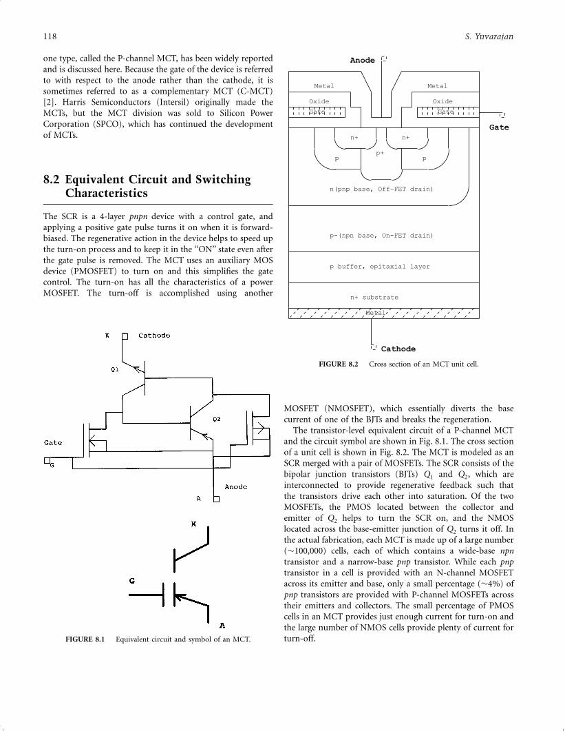
one type, called the P-channel MCT, has been widely reported
and is discussed here. Because the gate of the device is referred
to with respect to the anode rather than the cathode, it is
sometimes referred to as a complementary MCT (C-MCT)
[2]. Harris Semiconductors (Intersil) originally made the
MCTs, but the MCT division was sold to Silicon Power
Corporation (SPCO), which has continued the development
of MCTs.
8.2 Equivalent Circuit and SwitchingCharacteristics
The SCR is a 4-layer pnpn device with a control gate, and
applying a positive gate pulse turns it on when it is forward-
biased. The regenerative action in the device helps to speed up
the turn-on process and to keep it in the ‘‘ON’’ state even after
the gate pulse is removed. The MCT uses an auxiliary MOS
device (PMOSFET) to turn on and this simplifies the gate
control. The turn-on has all the characteristics of a power
MOSFET. The turn-off is accomplished using another
MOSFET (NMOSFET), which essentially diverts the base
current of one of the BJTs and breaks the regeneration.
The transistor-level equivalent circuit of a P-channel MCT
and the circuit symbol are shown in Fig. 8.1. The cross section
of a unit cell is shown in Fig. 8.2. The MCT is modeled as an
SCR merged with a pair of MOSFETs. The SCR consists of the
bipolar junction transistors (BJTs) Q1 and Q2, which are
interconnected to provide regenerative feedback such that
the transistors drive each other into saturation. Of the two
MOSFETs, the PMOS located between the collector and
emitter of Q2 helps to turn the SCR on, and the NMOS
located across the base-emitter junction of Q2 turns it off. In
the actual fabrication, each MCT is made up of a large number
(�100,000) cells, each of which contains a wide-base npn
transistor and a narrow-base pnp transistor. While each pnp
transistor in a cell is provided with an N-channel MOSFET
across its emitter and base, only a small percentage (�4%) of
pnp transistors are provided with P-channel MOSFETs across
their emitters and collectors. The small percentage of PMOS
cells in an MCT provides just enough current for turn-on and
the large number of NMOS cells provide plenty of current for
turn-off.FIGURE 8.1 Equivalent circuit and symbol of an MCT.
Gate
Metal
n+
p
Cathode
p+
Gate
p buffer, epitaxial layer
p-(npn base, On-FET drain)
n+ substrate
Oxide
p
Oxide
Gate
Metal
n(pnp base, Off-FET drain)
n+
Metal
Anode
FIGURE 8.2 Cross section of an MCT unit cell.
118 S. Yuvarajan
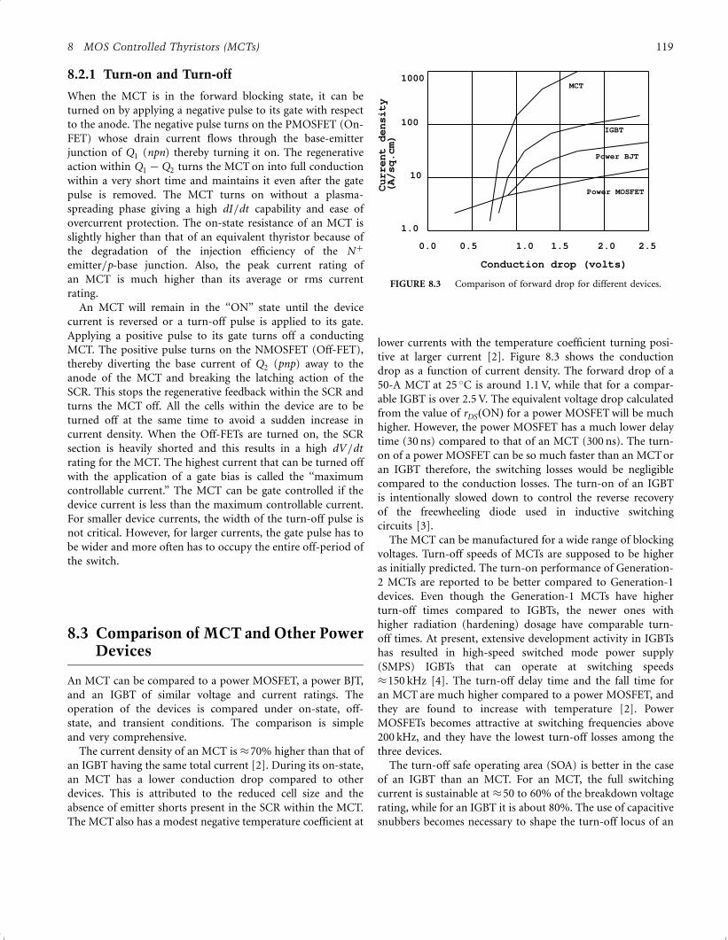
8.2.1 Turn-on and Turn-off
When the MCT is in the forward blocking state, it can be
turned on by applying a negative pulse to its gate with respect
to the anode. The negative pulse turns on the PMOSFET (On-
FET) whose drain current flows through the base-emitter
junction of Q1 (npn) thereby turning it on. The regenerative
action within Q1 ÿ Q2 turns the MCT on into full conduction
within a very short time and maintains it even after the gate
pulse is removed. The MCT turns on without a plasma-
spreading phase giving a high dI=dt capability and ease of
overcurrent protection. The on-state resistance of an MCT is
slightly higher than that of an equivalent thyristor because of
the degradation of the injection efficiency of the Nþ
emitter=p-base junction. Also, the peak current rating of
an MCT is much higher than its average or rms current
rating.
An MCT will remain in the ‘‘ON’’ state until the device
current is reversed or a turn-off pulse is applied to its gate.
Applying a positive pulse to its gate turns off a conducting
MCT. The positive pulse turns on the NMOSFET (Off-FET),
thereby diverting the base current of Q2 (pnp) away to the
anode of the MCT and breaking the latching action of the
SCR. This stops the regenerative feedback within the SCR and
turns the MCT off. All the cells within the device are to be
turned off at the same time to avoid a sudden increase in
current density. When the Off-FETs are turned on, the SCR
section is heavily shorted and this results in a high dV=dt
rating for the MCT. The highest current that can be turned off
with the application of a gate bias is called the ‘‘maximum
controllable current.’’ The MCT can be gate controlled if the
device current is less than the maximum controllable current.
For smaller device currents, the width of the turn-off pulse is
not critical. However, for larger currents, the gate pulse has to
be wider and more often has to occupy the entire off-period of
the switch.
8.3 Comparison of MCT and Other PowerDevices
An MCT can be compared to a power MOSFET, a power BJT,
and an IGBT of similar voltage and current ratings. The
operation of the devices is compared under on-state, off-
state, and transient conditions. The comparison is simple
and very comprehensive.
The current density of an MCT is �70% higher than that of
an IGBT having the same total current [2]. During its on-state,
an MCT has a lower conduction drop compared to other
devices. This is attributed to the reduced cell size and the
absence of emitter shorts present in the SCR within the MCT.
The MCT also has a modest negative temperature coefficient at
lower currents with the temperature coefficient turning posi-
tive at larger current [2]. Figure 8.3 shows the conduction
drop as a function of current density. The forward drop of a
50-A MCT at 25 �C is around 1.1 V, while that for a compar-
able IGBT is over 2.5 V. The equivalent voltage drop calculated
from the value of rDSðONÞ for a power MOSFET will be much
higher. However, the power MOSFET has a much lower delay
time (30 ns) compared to that of an MCT (300 ns). The turn-
on of a power MOSFET can be so much faster than an MCT or
an IGBT therefore, the switching losses would be negligible
compared to the conduction losses. The turn-on of an IGBT
is intentionally slowed down to control the reverse recovery
of the freewheeling diode used in inductive switching
circuits [3].
The MCT can be manufactured for a wide range of blocking
voltages. Turn-off speeds of MCTs are supposed to be higher
as initially predicted. The turn-on performance of Generation-
2 MCTs are reported to be better compared to Generation-1
devices. Even though the Generation-1 MCTs have higher
turn-off times compared to IGBTs, the newer ones with
higher radiation (hardening) dosage have comparable turn-
off times. At present, extensive development activity in IGBTs
has resulted in high-speed switched mode power supply
(SMPS) IGBTs that can operate at switching speeds
�150 kHz [4]. The turn-off delay time and the fall time for
an MCT are much higher compared to a power MOSFET, and
they are found to increase with temperature [2]. Power
MOSFETs becomes attractive at switching frequencies above
200 kHz, and they have the lowest turn-off losses among the
three devices.
The turn-off safe operating area (SOA) is better in the case
of an IGBT than an MCT. For an MCT, the full switching
current is sustainable at �50 to 60% of the breakdown voltage
rating, while for an IGBT it is about 80%. The use of capacitive
snubbers becomes necessary to shape the turn-off locus of an
Power MOSFET
0.0 0.5
1.0
MCT1000
100IGBT
Curr
ent
den
sity
(A
/sq.c
m)
Conduction drop (volts)
10
Power BJT
1.0 1.5 2.0 2.5
FIGURE 8.3 Comparison of forward drop for different devices.
8 MOS Controlled Thyristors (MCTs) 119
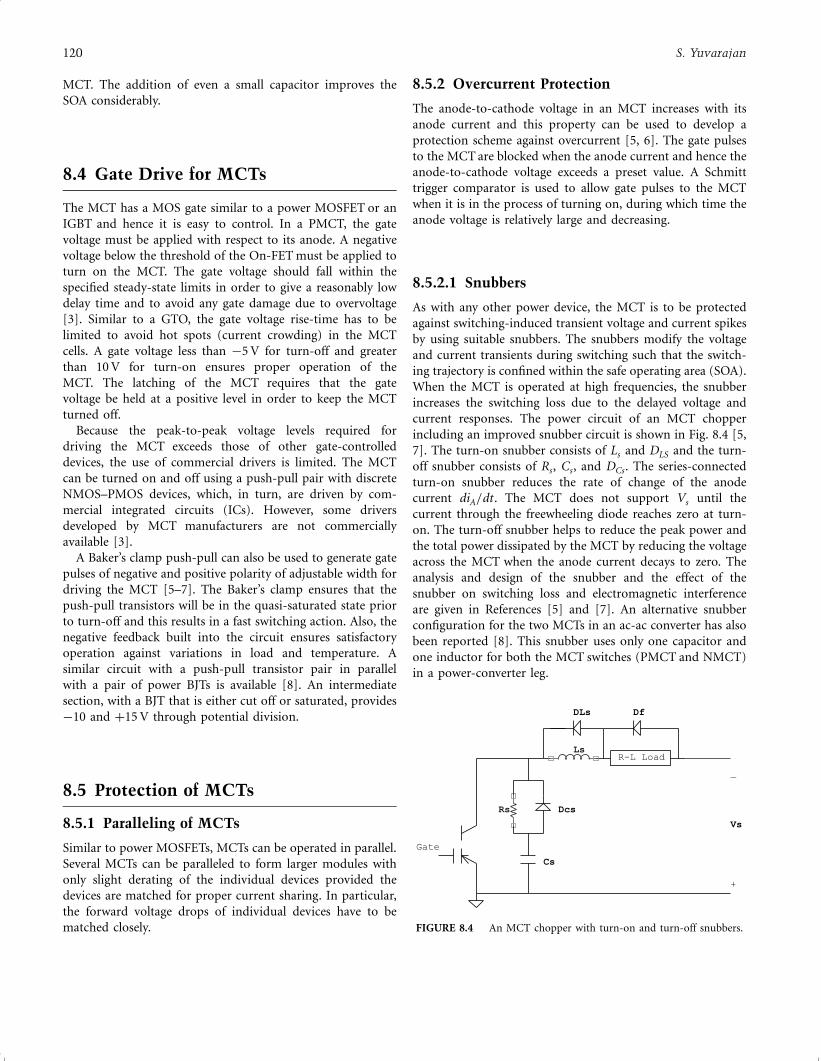
MCT. The addition of even a small capacitor improves the
SOA considerably.
8.4 Gate Drive for MCTs
The MCT has a MOS gate similar to a power MOSFET or an
IGBT and hence it is easy to control. In a PMCT, the gate
voltage must be applied with respect to its anode. A negative
voltage below the threshold of the On-FET must be applied to
turn on the MCT. The gate voltage should fall within the
specified steady-state limits in order to give a reasonably low
delay time and to avoid any gate damage due to overvoltage
[3]. Similar to a GTO, the gate voltage rise-time has to be
limited to avoid hot spots (current crowding) in the MCT
cells. A gate voltage less than ÿ5 V for turn-off and greater
than 10 V for turn-on ensures proper operation of the
MCT. The latching of the MCT requires that the gate
voltage be held at a positive level in order to keep the MCT
turned off.
Because the peak-to-peak voltage levels required for
driving the MCT exceeds those of other gate-controlled
devices, the use of commercial drivers is limited. The MCT
can be turned on and off using a push-pull pair with discrete
NMOS–PMOS devices, which, in turn, are driven by com-
mercial integrated circuits (ICs). However, some drivers
developed by MCT manufacturers are not commercially
available [3].
A Baker’s clamp push-pull can also be used to generate gate
pulses of negative and positive polarity of adjustable width for
driving the MCT [5–7]. The Baker’s clamp ensures that the
push-pull transistors will be in the quasi-saturated state prior
to turn-off and this results in a fast switching action. Also, the
negative feedback built into the circuit ensures satisfactory
operation against variations in load and temperature. A
similar circuit with a push-pull transistor pair in parallel
with a pair of power BJTs is available [8]. An intermediate
section, with a BJT that is either cut off or saturated, provides
ÿ10 and þ15 V through potential division.
8.5 Protection of MCTs
8.5.1 Paralleling of MCTs
Similar to power MOSFETs, MCTs can be operated in parallel.
Several MCTs can be paralleled to form larger modules with
only slight derating of the individual devices provided the
devices are matched for proper current sharing. In particular,
the forward voltage drops of individual devices have to be
matched closely.
8.5.2 Overcurrent Protection
The anode-to-cathode voltage in an MCT increases with its
anode current and this property can be used to develop a
protection scheme against overcurrent [5, 6]. The gate pulses
to the MCT are blocked when the anode current and hence the
anode-to-cathode voltage exceeds a preset value. A Schmitt
trigger comparator is used to allow gate pulses to the MCT
when it is in the process of turning on, during which time the
anode voltage is relatively large and decreasing.
8.5.2.1 Snubbers
As with any other power device, the MCT is to be protected
against switching-induced transient voltage and current spikes
by using suitable snubbers. The snubbers modify the voltage
and current transients during switching such that the switch-
ing trajectory is confined within the safe operating area (SOA).
When the MCT is operated at high frequencies, the snubber
increases the switching loss due to the delayed voltage and
current responses. The power circuit of an MCT chopper
including an improved snubber circuit is shown in Fig. 8.4 [5,
7]. The turn-on snubber consists of Ls and DLS and the turn-
off snubber consists of Rs, Cs, and DCs . The series-connected
turn-on snubber reduces the rate of change of the anode
current diA=dt . The MCT does not support Vs until the
current through the freewheeling diode reaches zero at turn-
on. The turn-off snubber helps to reduce the peak power and
the total power dissipated by the MCT by reducing the voltage
across the MCT when the anode current decays to zero. The
analysis and design of the snubber and the effect of the
snubber on switching loss and electromagnetic interference
are given in References [5] and [7]. An alternative snubber
configuration for the two MCTs in an ac-ac converter has also
been reported [8]. This snubber uses only one capacitor and
one inductor for both the MCT switches (PMCT and NMCT)
in a power-converter leg.
Df
Gate
Cs
Rs
Vs
Dcs
_
Ls
DLs
+
R-L Load
FIGURE 8.4 An MCT chopper with turn-on and turn-off snubbers.
120 S. Yuvarajan
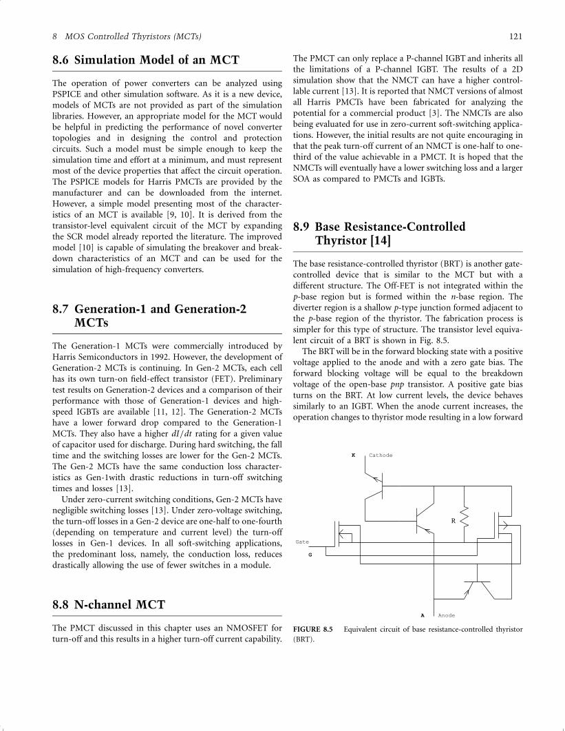
8.6 Simulation Model of an MCT
The operation of power converters can be analyzed using
PSPICE and other simulation software. As it is a new device,
models of MCTs are not provided as part of the simulation
libraries. However, an appropriate model for the MCT would
be helpful in predicting the performance of novel converter
topologies and in designing the control and protection
circuits. Such a model must be simple enough to keep the
simulation time and effort at a minimum, and must represent
most of the device properties that affect the circuit operation.
The PSPICE models for Harris PMCTs are provided by the
manufacturer and can be downloaded from the internet.
However, a simple model presenting most of the character-
istics of an MCT is available [9, 10]. It is derived from the
transistor-level equivalent circuit of the MCT by expanding
the SCR model already reported the literature. The improved
model [10] is capable of simulating the breakover and break-
down characteristics of an MCT and can be used for the
simulation of high-frequency converters.
8.7 Generation-1 and Generation-2MCTs
The Generation-1 MCTs were commercially introduced by
Harris Semiconductors in 1992. However, the development of
Generation-2 MCTs is continuing. In Gen-2 MCTs, each cell
has its own turn-on field-effect transistor (FET). Preliminary
test results on Generation-2 devices and a comparison of their
performance with those of Generation-1 devices and high-
speed IGBTs are available [11, 12]. The Generation-2 MCTs
have a lower forward drop compared to the Generation-1
MCTs. They also have a higher dI=dt rating for a given value
of capacitor used for discharge. During hard switching, the fall
time and the switching losses are lower for the Gen-2 MCTs.
The Gen-2 MCTs have the same conduction loss character-
istics as Gen-1with drastic reductions in turn-off switching
times and losses [13].
Under zero-current switching conditions, Gen-2 MCTs have
negligible switching losses [13]. Under zero-voltage switching,
the turn-off losses in a Gen-2 device are one-half to one-fourth
(depending on temperature and current level) the turn-off
losses in Gen-1 devices. In all soft-switching applications,
the predominant loss, namely, the conduction loss, reduces
drastically allowing the use of fewer switches in a module.
8.8 N-channel MCT
The PMCT discussed in this chapter uses an NMOSFET for
turn-off and this results in a higher turn-off current capability.
The PMCT can only replace a P-channel IGBT and inherits all
the limitations of a P-channel IGBT. The results of a 2D
simulation show that the NMCT can have a higher control-
lable current [13]. It is reported that NMCT versions of almost
all Harris PMCTs have been fabricated for analyzing the
potential for a commercial product [3]. The NMCTs are also
being evaluated for use in zero-current soft-switching applica-
tions. However, the initial results are not quite encouraging in
that the peak turn-off current of an NMCT is one-half to one-
third of the value achievable in a PMCT. It is hoped that the
NMCTs will eventually have a lower switching loss and a larger
SOA as compared to PMCTs and IGBTs.
8.9 Base Resistance-ControlledThyristor [14]
The base resistance-controlled thyristor (BRT) is another gate-
controlled device that is similar to the MCT but with a
different structure. The Off-FET is not integrated within the
p-base region but is formed within the n-base region. The
diverter region is a shallow p-type junction formed adjacent to
the p-base region of the thyristor. The fabrication process is
simpler for this type of structure. The transistor level equiva-
lent circuit of a BRT is shown in Fig. 8.5.
The BRT will be in the forward blocking state with a positive
voltage applied to the anode and with a zero gate bias. The
forward blocking voltage will be equal to the breakdown
voltage of the open-base pnp transistor. A positive gate bias
turns on the BRT. At low current levels, the device behaves
similarly to an IGBT. When the anode current increases, the
operation changes to thyristor mode resulting in a low forward
Cathode
A
Gate
G
Anode
K
R
FIGURE 8.5 Equivalent circuit of base resistance-controlled thyristor
(BRT).
8 MOS Controlled Thyristors (MCTs) 121
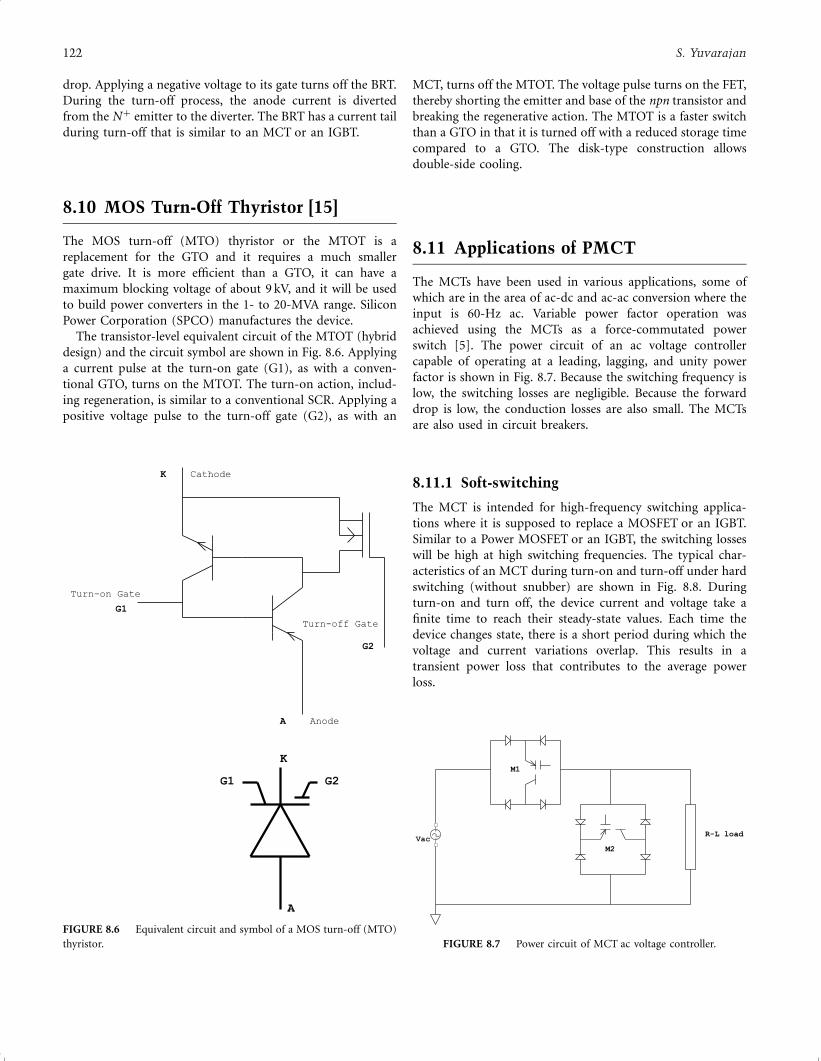
drop. Applying a negative voltage to its gate turns off the BRT.
During the turn-off process, the anode current is diverted
from the Nþ emitter to the diverter. The BRT has a current tail
during turn-off that is similar to an MCT or an IGBT.
8.10 MOS Turn-Off Thyristor [15]
The MOS turn-off (MTO) thyristor or the MTOT is a
replacement for the GTO and it requires a much smaller
gate drive. It is more efficient than a GTO, it can have a
maximum blocking voltage of about 9 kV, and it will be used
to build power converters in the 1- to 20-MVA range. Silicon
Power Corporation (SPCO) manufactures the device.
The transistor-level equivalent circuit of the MTOT (hybrid
design) and the circuit symbol are shown in Fig. 8.6. Applying
a current pulse at the turn-on gate (G1), as with a conven-
tional GTO, turns on the MTOT. The turn-on action, includ-
ing regeneration, is similar to a conventional SCR. Applying a
positive voltage pulse to the turn-off gate (G2), as with an
MCT, turns off the MTOT. The voltage pulse turns on the FET,
thereby shorting the emitter and base of the npn transistor and
breaking the regenerative action. The MTOT is a faster switch
than a GTO in that it is turned off with a reduced storage time
compared to a GTO. The disk-type construction allows
double-side cooling.
8.11 Applications of PMCT
The MCTs have been used in various applications, some of
which are in the area of ac-dc and ac-ac conversion where the
input is 60-Hz ac. Variable power factor operation was
achieved using the MCTs as a force-commutated power
switch [5]. The power circuit of an ac voltage controller
capable of operating at a leading, lagging, and unity power
factor is shown in Fig. 8.7. Because the switching frequency is
low, the switching losses are negligible. Because the forward
drop is low, the conduction losses are also small. The MCTs
are also used in circuit breakers.
8.11.1 Soft-switching
The MCT is intended for high-frequency switching applica-
tions where it is supposed to replace a MOSFET or an IGBT.
Similar to a Power MOSFET or an IGBT, the switching losses
will be high at high switching frequencies. The typical char-
acteristics of an MCT during turn-on and turn-off under hard
switching (without snubber) are shown in Fig. 8.8. During
turn-on and turn off, the device current and voltage take a
finite time to reach their steady-state values. Each time the
device changes state, there is a short period during which the
voltage and current variations overlap. This results in a
transient power loss that contributes to the average power
loss.
A
Turn-off Gate
Turn-on Gate
G1
Anode
K
G2
CathodeK
G2
G1
A
FIGURE 8.6 Equivalent circuit and symbol of a MOS turn-off (MTO)
thyristor.
M1
M2
R-L loadVac
FIGURE 8.7 Power circuit of MCT ac voltage controller.
122 S. Yuvarajan
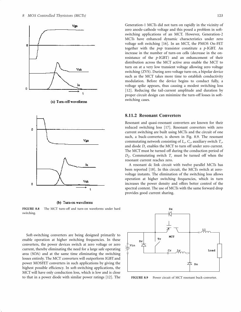
Soft-switching converters are being designed primarily to
enable operation at higher switching frequencies. In these
converters, the power devices switch at zero voltage or zero
current, thereby eliminating the need for a large safe operating
area (SOA) and at the same time eliminating the switching
losses entirely. The MCT converters will outperform IGBT and
power MOSFET converters in such applications by giving the
highest possible efficiency. In soft-switching applications, the
MCT will have only conduction loss, which is low and is close
to that in a power diode with similar power ratings [12]. The
Generation-1 MCTs did not turn on rapidly in the vicinity of
zero anode-cathode voltage and this posed a problem in soft-
switching applications of an MCT. However, Generation-2
MCTs have enhanced dynamic characteristics under zero
voltage soft switching [16]. In an MCT, the PMOS On-FET
together with the pnp transistor constitute a p-IGBT. An
increase in the number of turn-on cells (decrease in the on-
resistance of the p-IGBT) and an enhancement of their
distribution across the MCT active area enable the MCT to
turn on at a very low transient voltage allowing zero voltage
switching (ZVS). During zero voltage turn-on, a bipolar device
such as the MCT takes more time to establish conductivity
modulation. Before the device begins to conduct fully, a
voltage spike appears, thus causing a modest switching loss
[12]. Reducing the tail-current amplitude and duration by
proper circuit design can minimize the turn-off losses in soft-
switching cases.
8.11.2 Resonant Converters
Resonant and quasi-resonant converters are known for their
reduced switching loss [17]. Resonant converters with zero
current switching are built using MCTs and the circuit of one
such, a buck-converter, is shown in Fig. 8.9. The resonant
commutating network consisting of Lr , Cr , auxiliary switch Tr ,
and diode Dr enables the MCT to turn off under zero current.
The MCT must be turned off during the conduction period of
DZ . Commutating switch Tr must be turned off when the
resonant current reaches zero.
A resonant dc link circuit with twelve parallel MCTs has
been reported [18]. In this circuit, the MCTs switch at zero-
voltage instants. The elimination of the switching loss allows
operation at higher switching frequencies, which in turn
increases the power density and offers better control of the
spectral content. The use of MCTs with the same forward drop
provides good current sharing.
Vin
Dz
Cr LoadLr
Dr
MCT
L1
Do
Tr
FIGURE 8.9 Power circuit of MCT resonant buck-converter.
FIGURE 8.8 The MCT turn-off and turn-on waveforms under hard
switching.
8 MOS Controlled Thyristors (MCTs) 123
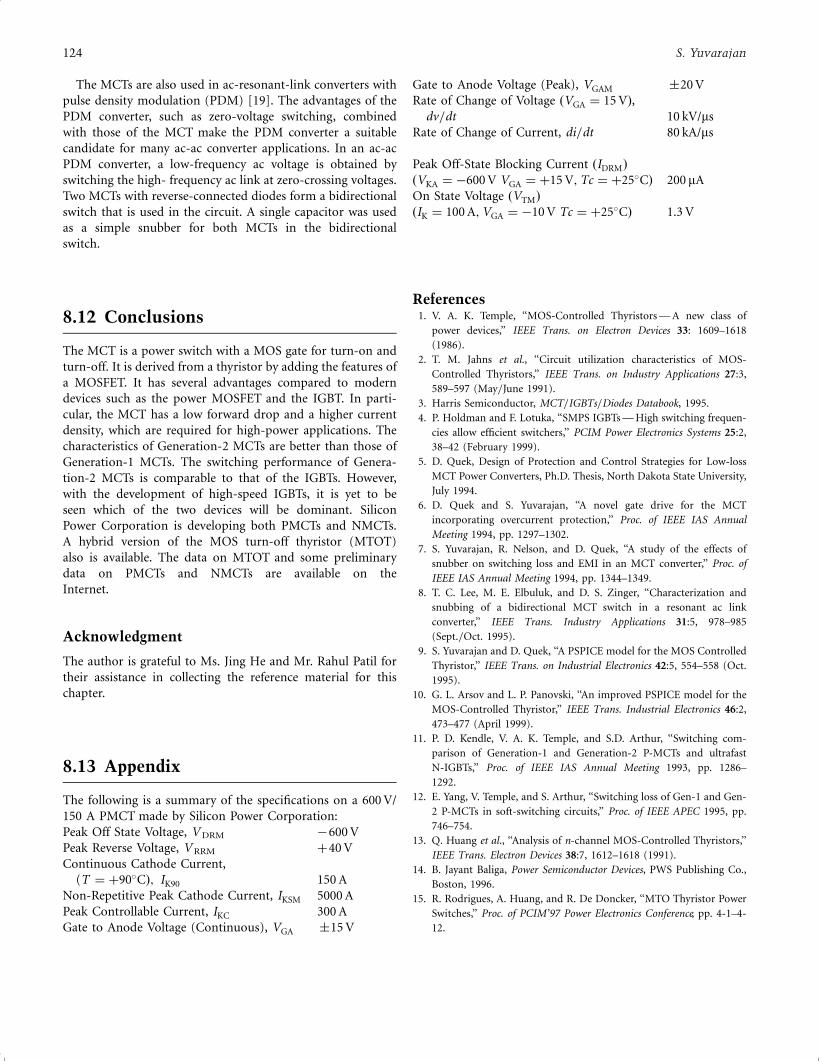
The MCTs are also used in ac-resonant-link converters with
pulse density modulation (PDM) [19]. The advantages of the
PDM converter, such as zero-voltage switching, combined
with those of the MCT make the PDM converter a suitable
candidate for many ac-ac converter applications. In an ac-ac
PDM converter, a low-frequency ac voltage is obtained by
switching the high- frequency ac link at zero-crossing voltages.
Two MCTs with reverse-connected diodes form a bidirectional
switch that is used in the circuit. A single capacitor was used
as a simple snubber for both MCTs in the bidirectional
switch.
8.12 Conclusions
The MCT is a power switch with a MOS gate for turn-on and
turn-off. It is derived from a thyristor by adding the features of
a MOSFET. It has several advantages compared to modern
devices such as the power MOSFET and the IGBT. In parti-
cular, the MCT has a low forward drop and a higher current
density, which are required for high-power applications. The
characteristics of Generation-2 MCTs are better than those of
Generation-1 MCTs. The switching performance of Genera-
tion-2 MCTs is comparable to that of the IGBTs. However,
with the development of high-speed IGBTs, it is yet to be
seen which of the two devices will be dominant. Silicon
Power Corporation is developing both PMCTs and NMCTs.
A hybrid version of the MOS turn-off thyristor (MTOT)
also is available. The data on MTOT and some preliminary
data on PMCTs and NMCTs are available on the
Internet.
Acknowledgment
The author is grateful to Ms. Jing He and Mr. Rahul Patil for
their assistance in collecting the reference material for this
chapter.
8.13 Appendix
The following is a summary of the specifications on a 600 V/
150 A PMCT made by Silicon Power Corporation:
Peak Off State Voltage, V DRM ÿ600 V
Peak Reverse Voltage, V RRM þ40 V
Continuous Cathode Current,
(T ¼ þ90�CÞ; IK90 150 A
Non-Repetitive Peak Cathode Current, IKSM 5000 A
Peak Controllable Current, IKC 300 A
Gate to Anode Voltage (Continuous), VGA �15 V
Gate to Anode Voltage (Peak), VGAM �20 V
Rate of Change of Voltage ðVGA ¼ 15 VÞ,
dv=dt 10 kV/ms
Rate of Change of Current, di=dt 80 kA/ms
Peak Off-State Blocking Current ðIDRMÞ
ðVKA ¼ ÿ600 V VGA ¼ þ15 V;Tc ¼ þ25�CÞ 200 mA
On State Voltage ðVTMÞ
ðIK ¼ 100 A;VGA ¼ ÿ10 V Tc ¼ þ25�CÞ 1.3 V
References1. V. A. K. Temple, ‘‘MOS-Controlled Thyristors — A new class of
power devices,’’ IEEE Trans. on Electron Devices 33: 1609–1618
(1986).
2. T. M. Jahns et al., ‘‘Circuit utilization characteristics of MOS-
Controlled Thyristors,’’ IEEE Trans. on Industry Applications 27:3,
589–597 (May=June 1991).
3. Harris Semiconductor, MCT=IGBTs=Diodes Databook, 1995.
4. P. Holdman and F. Lotuka, ‘‘SMPS IGBTs — High switching frequen-
cies allow efficient switchers,’’ PCIM Power Electronics Systems 25:2,
38–42 (February 1999).
5. D. Quek, Design of Protection and Control Strategies for Low-loss
MCT Power Converters, Ph.D. Thesis, North Dakota State University,
July 1994.
6. D. Quek and S. Yuvarajan, ‘‘A novel gate drive for the MCT
incorporating overcurrent protection,’’ Proc. of IEEE IAS Annual
Meeting 1994, pp. 1297–1302.
7. S. Yuvarajan, R. Nelson, and D. Quek, ‘‘A study of the effects of
snubber on switching loss and EMI in an MCT converter,’’ Proc. of
IEEE IAS Annual Meeting 1994, pp. 1344–1349.
8. T. C. Lee, M. E. Elbuluk, and D. S. Zinger, ‘‘Characterization and
snubbing of a bidirectional MCT switch in a resonant ac link
converter,’’ IEEE Trans. Industry Applications 31:5, 978–985
(Sept.=Oct. 1995).
9. S. Yuvarajan and D. Quek, ‘‘A PSPICE model for the MOS Controlled
Thyristor,’’ IEEE Trans. on Industrial Electronics 42:5, 554–558 (Oct.
1995).
10. G. L. Arsov and L. P. Panovski, ‘‘An improved PSPICE model for the
MOS-Controlled Thyristor,’’ IEEE Trans. Industrial Electronics 46:2,
473–477 (April 1999).
11. P. D. Kendle, V. A. K. Temple, and S.D. Arthur, ‘‘Switching com-
parison of Generation-1 and Generation-2 P-MCTs and ultrafast
N-IGBTs,’’ Proc. of IEEE IAS Annual Meeting 1993, pp. 1286–
1292.
12. E. Yang, V. Temple, and S. Arthur, ‘‘Switching loss of Gen-1 and Gen-
2 P-MCTs in soft-switching circuits,’’ Proc. of IEEE APEC 1995, pp.
746–754.
13. Q. Huang et al., ‘‘Analysis of n-channel MOS-Controlled Thyristors,’’
IEEE Trans. Electron Devices 38:7, 1612–1618 (1991).
14. B. Jayant Baliga, Power Semiconductor Devices, PWS Publishing Co.,
Boston, 1996.
15. R. Rodrigues, A. Huang, and R. De Doncker, ‘‘MTO Thyristor Power
Switches,’’ Proc. of PCIM’97 Power Electronics Conference, pp. 4-1–4-
12.
124 S. Yuvarajan

16. R. De Doncker et al., ‘‘Characteristics of MOS-Controlled Thyristors
under zero voltage soft-switching conditions,’’ IEEE Trans. Industry
Applications 28:2, 387–394 (March=April 1992).
17. A. Dmowski et al., ‘‘Design of a buck converter with zero-current
turn-off MCT,’’ Proc. IEEE IAS Annual Meeting 1994, pp. 1025–
1030.
18. H.-R. Chang and A. V. Radun, ‘‘Performance of 500 V, 450 A Parallel
MOS Controlled Thyristors (MCTs) in a resonant dc-link circuit,’’
Proc. IEEE IAS Annual Meeting 1990, pp. 1613–1617.
19. M. E. Elbuluk, D. S. Zinger, and T. Lee, ‘‘Performance of MCT’s in a
current-regulated ac=ac PDM converter,’’ IEEE Trans. Power Electro-
nics 11:1, 49–56 (January 1996).
8 MOS Controlled Thyristors (MCTs) 125
9Static Induction Devices
Bogdan M. Wilamowski, Ph.D.College of Engineering,
University of Idaho, Boise,
ID 83712 USA
Summary
Several devices from the static induction family including
static induction transistors (SIT), static induction diodes
(SID), static induction thyristors, lateral punch-through tran-
sistors (LPTT), static induction transistor logic (SITL), static
induction MOS transistors (SIMOS), and space charge limit-
ing load (SCLL) are described. The theory of operation of
static induction devices is given for both a current controlled
by a potential barrier and a current controlled by space
charge. The new concept of a punch-through emitter
(PTE), which operates with majority carrier transport, is
presented.
9.1 Introduction
Static induction devices were invented by Nishizawa [28]. The
idea was so innovative that the establishment in the solid-state
electronics community at the time had difficulty understand-
ing and accepting this discovery. Japan was the only country
where static induction family devices were successfully fabri-
cated [14]. The number of devices in this family continues to
grow with time. Static induction transistors can operate with a
power of 100 kW at 100 kHz or 10 W at 10 GHz. Static
induction transistor logic had switching energy 100� smaller
than its I2L competitor [8, 9]. The static induction thyristor
has many advantages over the traditional SCR, and the static
induction diode exhibits high switching speed, large reverse
voltage, and low forward voltage drops.
9.2 Theory of Static Induction Devices
The cross section of the static induction transistor is shown in
Fig. 9.1, while its characteristics are shown in Fig. 9.2. An
induced electrostatically potential barrier controls the current
in static induction devices. The derivations of formulas will be
done for an n-channel device, but the obtained results with a
little modification also can be applied to p-channel devices.
For a small electrical field existing in the vicinity of the
potential barrier, the drift and diffusion current can be
approximated by
Jn ¼ ÿqnðxÞmn
djðxÞdxþ qDn
dnðxÞ
dxð9:1Þ
Copyright # 2001 by Academic Press.
All rights of reproduction in any form reserved.
127
Summary ................................................................................................... 127
9.1 Introduction ...................................................................................... 127
9.2 Theory of Static Induction Devices........................................................ 128
9.3 Characteristics of Static Induction Transistor .......................................... 130
9.4 Bipolar Mode Operation of SI Devices (BSIT) ........................................ 130
9.5 Emitters for Static Induction Devices..................................................... 131
9.6 Static Induction Diode (SID) ............................................................... 131
9.7 Lateral Punch-Through Transistor (LPTT).............................................. 132
9.8 Static Induction Transistor Logic (SITL) ................................................ 132
9.9 BJT Saturation Protected by SIT ........................................................... 133
9.10 Static Induction MOS Transistor (SIMOS) ............................................. 133
9.11 Space-Charge Limiting Load (SCLL)...................................................... 134
9.12 Power MOS Transistors ....................................................................... 134
9.13 Static Induction Thyristor .................................................................... 135
9.14 Gate Turn-Off Thyristor (GTO) ............................................................ 136
References.......................................................................................... 136
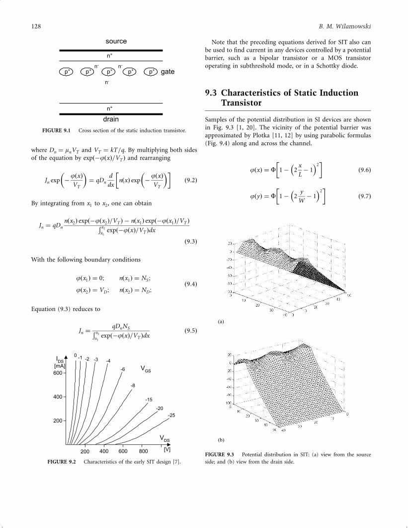
where Dn ¼ mnVT and VT ¼ kT=q. By multiplying both sides
of the equation by expðÿjðxÞ=VT Þ and rearranging
Jn exp ÿjðxÞVT
� �¼ qDn
d
dxnðxÞ exp ÿ
jðxÞVT
� �� �ð9:2Þ
By integrating from x1 to x2, one can obtain
Jn ¼ qDn
nðx2Þ expðÿjðx2Þ=VT Þ ÿ nðx1Þ expðÿjðx1Þ=VT Þ� x2
x1expðÿjðxÞ=VT Þdx
ð9:3Þ
With the following boundary conditions
jðx1Þ ¼ 0; nðx1Þ ¼ NS;
jðx2Þ ¼ VD; nðx2Þ ¼ ND;ð9:4Þ
Equation (9.3) reduces to
Jn ¼qDnNS� x2
x1expðÿjðxÞ=VT Þdx
ð9:5Þ
Note that the preceding equations derived for SIT also can
be used to find current in any devices controlled by a potential
barrier, such as a bipolar transistor or a MOS transistor
operating in subthreshold mode, or in a Schottky diode.
9.3 Characteristics of Static InductionTransistor
Samples of the potential distribution in SI devices are shown
in Fig. 9.3 [1, 20]. The vicinity of the potential barrier was
approximated by Plotka [11, 12] by using parabolic formulas
(Fig. 9.4) along and across the channel.
jðxÞ ¼ F 1ÿ 2x
Lÿ 1
� �2� �
ð9:6Þ
jðyÞ ¼ F 1ÿ 2y
Wÿ 1
� �2� �
ð9:7Þ
n+
p+
n+
p+p+ p+ p+n-
n-
n-
source
drain
gate
FIGURE 9.1 Cross section of the static induction transistor.
VDS
IDS
VGS
0-1 -2 -3 -4
-6
-8
-15
-20
-25
[V]
[mA]
400
600
200
200 400 600 800
FIGURE 9.2 Characteristics of the early SIT design [7].
(a)
(b)
FIGURE 9.3 Potential distribution in SIT: (a) view from the source
side; and (b) view from the drain side.
128 B. M. Wilamowski
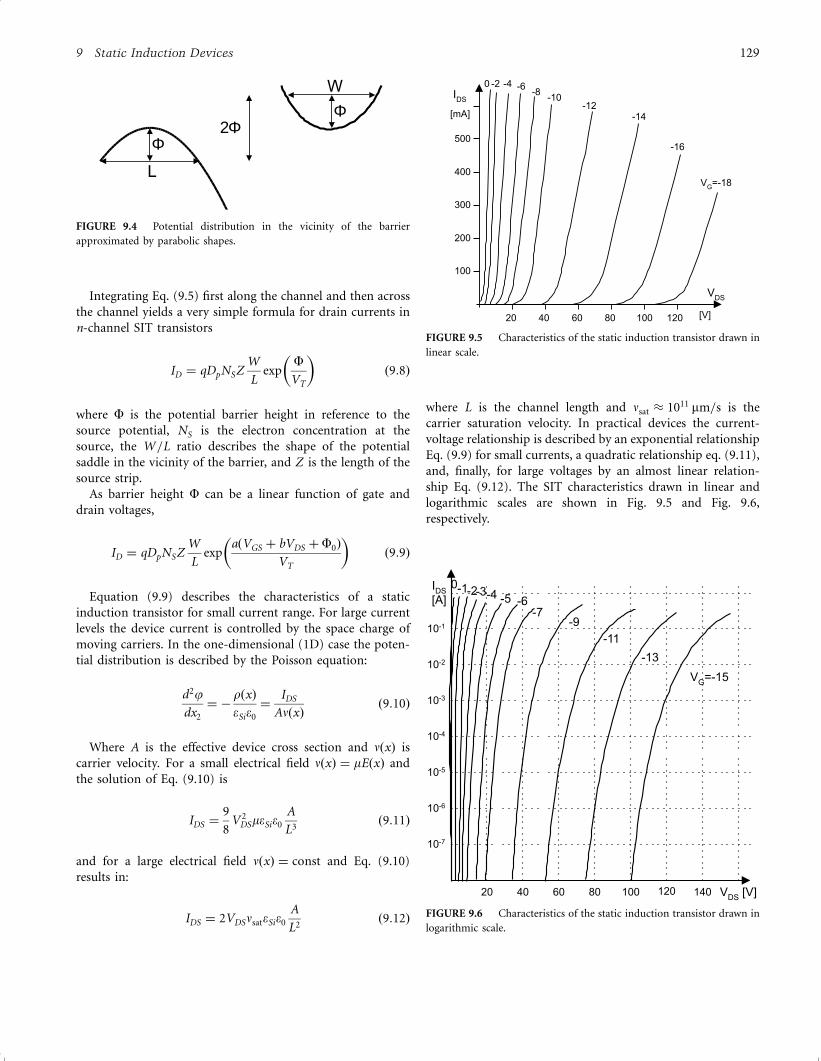
Integrating Eq. (9.5) first along the channel and then across
the channel yields a very simple formula for drain currents in
n-channel SIT transistors
ID ¼ qDpNSZW
Lexp
FVT
� �ð9:8Þ
where F is the potential barrier height in reference to the
source potential, NS is the electron concentration at the
source, the W=L ratio describes the shape of the potential
saddle in the vicinity of the barrier, and Z is the length of the
source strip.
As barrier height F can be a linear function of gate and
drain voltages,
ID ¼ qDpNSZW
Lexp
aðVGS þ bVDS þ F0Þ
VT
� �ð9:9Þ
Equation (9.9) describes the characteristics of a static
induction transistor for small current range. For large current
levels the device current is controlled by the space charge of
moving carriers. In the one-dimensional (1D) case the poten-
tial distribution is described by the Poisson equation:
d2jdx2
¼ ÿrðxÞeSie0
¼IDS
AnðxÞð9:10Þ
Where A is the effective device cross section and nðxÞ is
carrier velocity. For a small electrical field nðxÞ ¼ mEðxÞ and
the solution of Eq. (9.10) is
IDS ¼9
8V 2
DSmeSie0
A
L3ð9:11Þ
and for a large electrical field nðxÞ ¼ const and Eq. (9.10)
results in:
IDS ¼ 2VDSnsateSie0
A
L2ð9:12Þ
where L is the channel length and nsat � 1011 mm=s is the
carrier saturation velocity. In practical devices the current-
voltage relationship is described by an exponential relationship
Eq. (9.9) for small currents, a quadratic relationship eq. (9.11),
and, finally, for large voltages by an almost linear relation-
ship Eq. (9.12). The SIT characteristics drawn in linear and
logarithmic scales are shown in Fig. 9.5 and Fig. 9.6,
respectively.
VDS
IDS
[mA]
[V]
VG=-18
-16
-14-12
-10-8
-6-4-20
20 40 60 80 100 120
100
500
300
200
400
FIGURE 9.5 Characteristics of the static induction transistor drawn in
linear scale.
VG=-15
-13
-11
-9-7
-6-5-4-3-2-10
10-3
10-1
10-2
10-4
10-5
10-6
10-7
20 40 60 80 100 120 140
IDS
[A]
VDS
[V]
FIGURE 9.6 Characteristics of the static induction transistor drawn in
logarithmic scale.
L
Φ
ΦW
2Φ
FIGURE 9.4 Potential distribution in the vicinity of the barrier
approximated by parabolic shapes.
9 Static Induction Devices 129
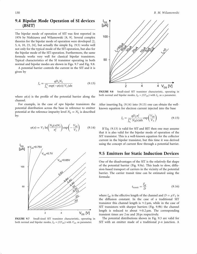
9.4 Bipolar Mode Operation of SI devices(BSIT)
The bipolar mode of operation of SIT was first reported in
1976 by Nishizawa and Wilamowski [8, 9]. Several complex
theories for the bipolar mode of operation were developed [2,
5, 6, 10, 23, 24], but actually the simple Eq. (9.5) works well
not only for the typical mode of the SIT operation, but also for
the bipolar mode of the SIT operation. Furthermore, the same
formula works very well for classical bipolar transistors.
Typical characteristics of the SI transistor operating in both
normal and bipolar modes are shown in Figs. 9.7 and Fig. 9.8.
A potential barrier controls the current in the SIT and it is
given by
Jn ¼qDnNS� x2
x1expðÿjðxÞ=VT Þdx
ð9:13Þ
where jðxÞ is the profile of the potential barrier along the
channel.
For example, in the case of npn bipolar transistors the
potential distribution across the base in reference to emitter
potential at the reference impurity level NE ¼ NS is described
by:
jðxÞ ¼ VT lnNBðxÞNS
n2i
� �exp ÿ
VBE
VT
� �ð9:14Þ
After inserting Eq. (9.14) into (9.13) one can obtain the well-
known equation for electron current injected into the base
Jn ¼qDnn2
i� x2
x1NBðxÞdx
expVBE
VT
� �ð9:15Þ
If Eq. (9.13) is valid for SIT and BJT then one may assume
that it is also valid for the bipolar mode of operation of the
SIT transistor. This is a well-known equation for the collector
current in the bipolar transistor, but this time it was derived
using the concept of current flow through a potential barrier.
9.5 Emitters for Static Induction Devices
One of the disadvantages of the SIT is the relatively flat shape
of the potential barrier (Fig. 9.9a). This leads to slow, diffu-
sion-based transport of carriers in the vicinity of the potential
barrier. The carrier transit time can be estimated using the
formula:
ttransit ¼l2eff
Dð9:16Þ
where leff is the effective length of the channel and D ¼ mVT is
the diffusion constant. In the case of a traditional SIT
transistor this channel length is �2 mm, while in the case of
SIT transistors with sharper barriers (Fig. 9.9b) the channel
length is reduced to about �0:2 mm. The corresponding
transient times are 2 ns and 20 ps respectively.
The potential distributions shown in Fig. 9.3 are valid for
SIT with an emitter made of a traditional p-n junction. A
VDS
[V]
IDS
[µA]
100
50
2 4
VGS
=0.65V
VGS
=0.7V
VGS
=0.75V
0.6V
0.5V
0.3V
0V
-0.5
V
-1V
-2V
-3V
0.4V
FIGURE 9.7 Small-sized SIT transistor characteristic, operating in
both normal and bipolar modes, ID ¼ f ðVDSÞ with VGS as parameter.
I G=02µA
5µA10
µA20
µA30
µA40
µAI G
=50µA
IDS
[µA]
VDS
[V]
50
100
2 4 4
FIGURE 9.8 Small-sized SIT transistor characteristic, operating in
both normal and bipolar modes, ID ¼ f ðVDSÞ with IG as a parameter.
130 B. M. Wilamowski
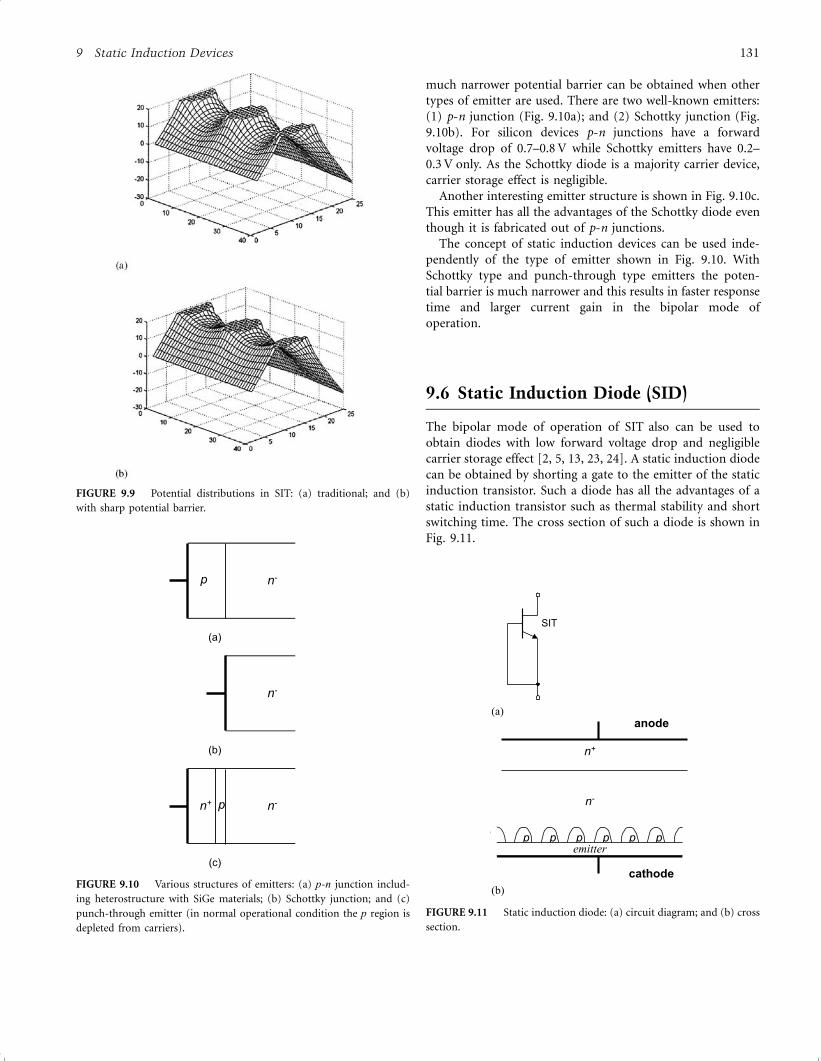
much narrower potential barrier can be obtained when other
types of emitter are used. There are two well-known emitters:
(1) p-n junction (Fig. 9.10a); and (2) Schottky junction (Fig.
9.10b). For silicon devices p-n junctions have a forward
voltage drop of 0.7–0.8 V while Schottky emitters have 0.2–
0.3 V only. As the Schottky diode is a majority carrier device,
carrier storage effect is negligible.
Another interesting emitter structure is shown in Fig. 9.10c.
This emitter has all the advantages of the Schottky diode even
though it is fabricated out of p-n junctions.
The concept of static induction devices can be used inde-
pendently of the type of emitter shown in Fig. 9.10. With
Schottky type and punch-through type emitters the poten-
tial barrier is much narrower and this results in faster response
time and larger current gain in the bipolar mode of
operation.
9.6 Static Induction Diode (SID)
The bipolar mode of operation of SIT also can be used to
obtain diodes with low forward voltage drop and negligible
carrier storage effect [2, 5, 13, 23, 24]. A static induction diode
can be obtained by shorting a gate to the emitter of the static
induction transistor. Such a diode has all the advantages of a
static induction transistor such as thermal stability and short
switching time. The cross section of such a diode is shown in
Fig. 9.11.
FIGURE 9.9 Potential distributions in SIT: (a) traditional; and (b)
with sharp potential barrier.
p n-
n-
p n-n+
(a)
(b)
(c)
FIGURE 9.10 Various structures of emitters: (a) p-n junction includ-
ing heterostructure with SiGe materials; (b) Schottky junction; and (c)
punch-through emitter (in normal operational condition the p region is
depleted from carriers).
SIT
(a)
n-
n+
p p p p p p
emitter
anode
cathode
(b)
FIGURE 9.11 Static induction diode: (a) circuit diagram; and (b) cross
section.
9 Static Induction Devices 131
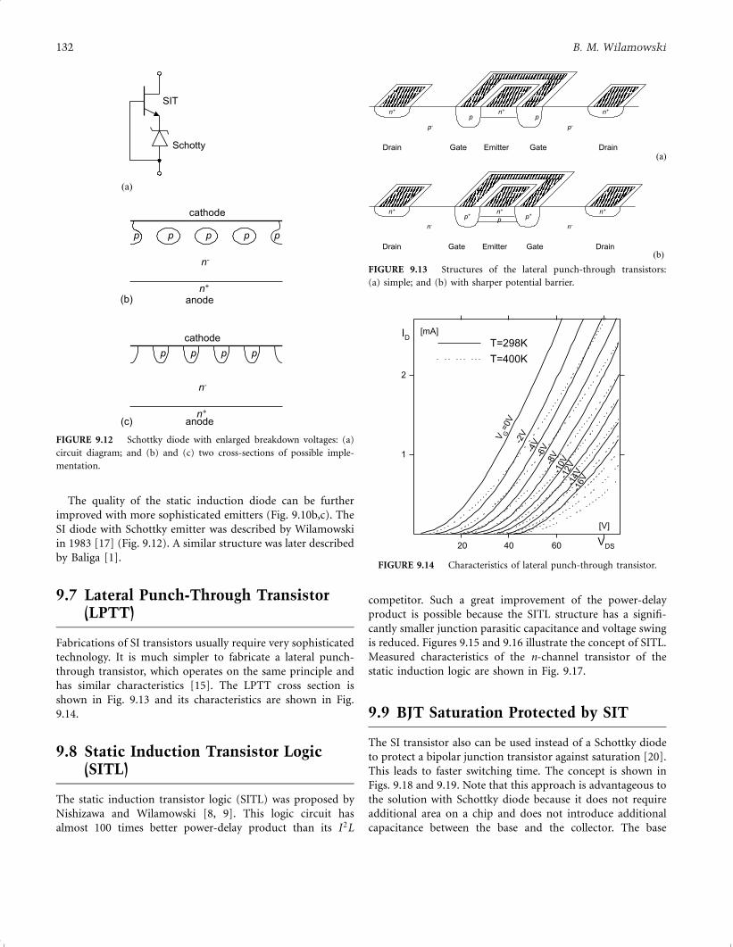
The quality of the static induction diode can be further
improved with more sophisticated emitters (Fig. 9.10b,c). The
SI diode with Schottky emitter was described by Wilamowski
in 1983 [17] (Fig. 9.12). A similar structure was later described
by Baliga [1].
9.7 Lateral Punch-Through Transistor(LPTT)
Fabrications of SI transistors usually require very sophisticated
technology. It is much simpler to fabricate a lateral punch-
through transistor, which operates on the same principle and
has similar characteristics [15]. The LPTT cross section is
shown in Fig. 9.13 and its characteristics are shown in Fig.
9.14.
9.8 Static Induction Transistor Logic(SITL)
The static induction transistor logic (SITL) was proposed by
Nishizawa and Wilamowski [8, 9]. This logic circuit has
almost 100 times better power-delay product than its I2L
competitor. Such a great improvement of the power-delay
product is possible because the SITL structure has a signifi-
cantly smaller junction parasitic capacitance and voltage swing
is reduced. Figures 9.15 and 9.16 illustrate the concept of SITL.
Measured characteristics of the n-channel transistor of the
static induction logic are shown in Fig. 9.17.
9.9 BJT Saturation Protected by SIT
The SI transistor also can be used instead of a Schottky diode
to protect a bipolar junction transistor against saturation [20].
This leads to faster switching time. The concept is shown in
Figs. 9.18 and 9.19. Note that this approach is advantageous to
the solution with Schottky diode because it does not require
additional area on a chip and does not introduce additional
capacitance between the base and the collector. The base
SIT
Schotty
(a)
p
n-
n+
pp p p
p
n-
n+
ppp
cathode
anode
anode(b)
(c)
FIGURE 9.12 Schottky diode with enlarged breakdown voltages: (a)
circuit diagram; and (b) and (c) two cross-sections of possible imple-
mentation.
n+
p-
p
Emitter Gate DrainDrain Gate
pn+
p-
n+
(a)
n+
n-
Emitter Gate DrainDrain Gate
p+n+ n+
n-
pp+
(b)
FIGURE 9.13 Structures of the lateral punch-through transistors:
(a) simple; and (b) with sharper potential barrier.
T=298K
T=400K
-2VV G
=0V
-4V
-6V
-8V
-10V
-12V
-14V
-16V
[mA]ID
2
1
[V]
VDS20 40 60
FIGURE 9.14 Characteristics of lateral punch-through transistor.
132 B. M. Wilamowski
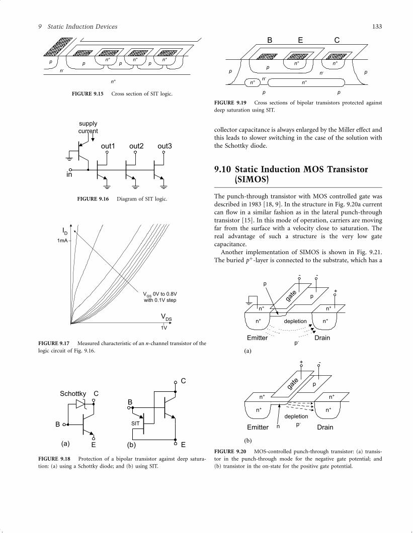
collector capacitance is always enlarged by the Miller effect and
this leads to slower switching in the case of the solution with
the Schottky diode.
9.10 Static Induction MOS Transistor(SIMOS)
The punch-through transistor with MOS controlled gate was
described in 1983 [18, 9]. In the structure in Fig. 9.20a current
can flow in a similar fashion as in the lateral punch-through
transistor [15]. In this mode of operation, carriers are moving
far from the surface with a velocity close to saturation. The
real advantage of such a structure is the very low gate
capacitance.
Another implementation of SIMOS is shown in Fig. 9.21.
The buried pþ-layer is connected to the substrate, which has a
VDS
ID
1V
1mA
VGS
0V to 0.8V
with 0.1V step
FIGURE 9.17 Measured characteristic of an n-channel transistor of the
logic circuit of Fig. 9.16.
n+
n-
pp
n+ n+ n+
pp
FIGURE 9.15 Cross section of SIT logic.
out1
in
out2 out3
supply
current
FIGURE 9.16 Diagram of SIT logic.
B
C
E
Schottky
(a)
B
C
E
SIT
(b)
FIGURE 9.18 Protection of a bipolar transistor against deep satura-
tion: (a) using a Schottky diode; and (b) using SIT.
n+n-
pp
n+n+
n+
p
p p
n-
B E C
FIGURE 9.19 Cross sections of bipolar transistors protected against
deep saturation using SIT.
Emitter Drain
n+
p
n+ n+
n+
gate
-
p
depletion
+
-
p-
(a)
Emitter Drainp-
n+
p
n+ n+
n+
gate
-+
n
depletion
(b)
FIGURE 9.20 MOS-controlled punch-through transistor: (a) transis-
tor in the punch-through mode for the negative gate potential; and
(b) transistor in the on-state for the positive gate potential.
9 Static Induction Devices 133
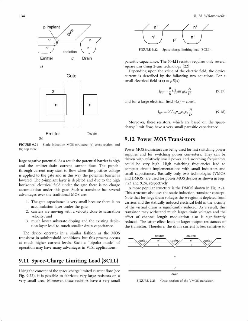
large negative potential. As a result the potential barrier is high
and the emitter-drain current cannot flow. The punch-
through current may start to flow when the positive voltage
is applied to the gate and in this way the potential barrier is
lowered. The p-implant layer is depleted and due to the high
horizontal electrical field under the gate there is no charge
accumulation under this gate. Such a transistor has several
advantages over the traditional MOS are:
1. The gate capacitance is very small because there is no
accumulation layer under the gate;
2. carriers are moving with a velocity close to saturation
velocity; and
3. much lower substrate doping and the existing deple-
tion layer lead to much smaller drain capacitance.
The device operates in a similar fashion as the MOS
transistor in subthreshold conditions, but this process occurs
at much higher current levels. Such a ‘‘bipolar mode’’ of
operation may have many advantages in VLSI applications.
9.11 Space-Charge Limiting Load (SCLL)
Using the concept of the space-charge limited current flow (see
Fig. 9.22), it is possible to fabricate very large resistors on a
very small area. Moreover, these resistors have a very small
parasitic capacitance. The 50-kO resistor requires only several
square mm using 2-mm technology [22].
Depending upon the value of the electric field, the device
current is described by the following two equations. For a
small electrical field nðxÞ ¼ mEðxÞ
IDS ¼9
8V 2
DSmeSie0
A
L3ð9:17Þ
and for a large electrical field nðxÞ ¼ const,
IDS ¼ 2VDSnsateSie0
A
L2ð9:18Þ
Moreover, these resistors, which are based on the space-
charge limit flow, have a very small parasitic capacitance.
9.12 Power MOS Transistors
Power MOS transistors are being used for fast switching power
supplies and for switching power converters. They can be
driven with relatively small power and switching frequencies
could be very high. High switching frequencies lead to
compact circuit implementations with small inductors and
small capacitances. Basically only two technologies (VMOS
and DMOS) are used for power MOS devices as shown in Figs.
9.23 and 9.24, respectively.
A more popular structure is the DMOS shown in Fig. 9.24.
This structure also uses the static induction transistor concept.
Note that for large drain voltages the n-region is depleted from
carriers and the statically induced electrical field in the vicinity
of the virtual drain is significantly reduced. As a result, this
transistor may withstand much larger drain voltages and the
effect of channel length modulation also is significantly
reduced. The latter effect leads to larger output resistances of
the transistor. Therefore, the drain current is less sensitive to
Emitter Drainp-
p+
n+ n+
n+
p implant
depletion
gate
(a)
Emitter Drain
n
Gate
p
n
(b)
FIGURE 9.21 Static induction MOS structure: (a) cross section; and
(b) top view.
p-
n+
n+
n+
n+
FIGURE 9.22 Space-charge limiting load (SCLL).
n+
n+
n-
pp
n+gate gate gate
source source
drain
FIGURE 9.23 Cross section of the VMOS transistor.
134 B. M. Wilamowski
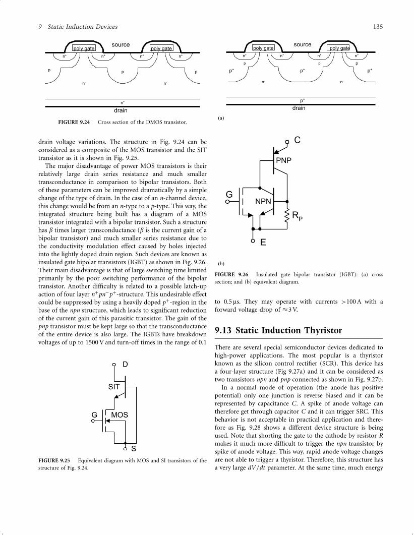
drain voltage variations. The structure in Fig. 9.24 can be
considered as a composite of the MOS transistor and the SIT
transistor as it is shown in Fig. 9.25.
The major disadvantage of power MOS transistors is their
relatively large drain series resistance and much smaller
transconductance in comparison to bipolar transistors. Both
of these parameters can be improved dramatically by a simple
change of the type of drain. In the case of an n-channel device,
this change would be from an n-type to a p-type. This way, the
integrated structure being built has a diagram of a MOS
transistor integrated with a bipolar transistor. Such a structure
has b times larger transconductance (b is the current gain of a
bipolar transistor) and much smaller series resistance due to
the conductivity modulation effect caused by holes injected
into the lightly doped drain region. Such devices are known as
insulated gate bipolar transistors (IGBT) as shown in Fig. 9.26.
Their main disadvantage is that of large switching time limited
primarily by the poor switching performance of the bipolar
transistor. Another difficulty is related to a possible latch-up
action of four layer nþpnÿpþ-structure. This undesirable effect
could be suppressed by using a heavily doped pþ-region in the
base of the npn structure, which leads to significant reduction
of the current gain of this parasitic transistor. The gain of the
pnp transistor must be kept large so that the transconductance
of the entire device is also large. The IGBTs have breakdown
voltages of up to 1500 V and turn-off times in the range of 0.1
to 0.5 ms. They may operate with currents >100 A with a
forward voltage drop of �3 V.
9.13 Static Induction Thyristor
There are several special semiconductor devices dedicated to
high-power applications. The most popular is a thyristor
known as the silicon control rectifier (SCR). This device has
a four-layer structure (Fig 9.27a) and it can be considered as
two transistors npn and pnp connected as shown in Fig. 9.27b.
In a normal mode of operation (the anode has positive
potential) only one junction is reverse biased and it can be
represented by capacitance C. A spike of anode voltage can
therefore get through capacitor C and it can trigger SRC. This
behavior is not acceptable in practical application and there-
fore as Fig. 9.28 shows a different device structure is being
used. Note that shorting the gate to the cathode by resistor R
makes it much more difficult to trigger the npn transistor by
spike of anode voltage. This way, rapid anode voltage changes
are not able to trigger a thyristor. Therefore, this structure has
a very large dV=dt parameter. At the same time, much energy
n+ n+ n+ n+
n+
p pp
n- n-
poly gatesource
drain
poly gate
FIGURE 9.24 Cross section of the DMOS transistor.
SIT
MOS
S
G
D
FIGURE 9.25 Equivalent diagram with MOS and SI transistors of the
structure of Fig. 9.24.
poly gatesource
drain
n+ n+ n+ n+
p pp
n- n-
p+ p+p+
p+
poly gate
(a)
RP
E
G
C
NPN
PNP
(b)
FIGURE 9.26 Insulated gate bipolar transistor (IGBT): (a) cross
section; and (b) equivalent diagram.
9 Static Induction Devices 135
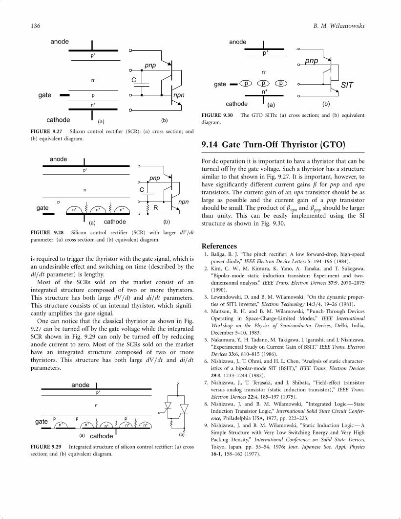
is required to trigger the thyristor with the gate signal, which is
an undesirable effect and switching on time (described by the
di=dt parameter) is lengthy.
Most of the SCRs sold on the market consist of an
integrated structure composed of two or more thyristors.
This structure has both large dV=dt and di=dt parameters.
This structure consists of an internal thyristor, which signifi-
cantly amplifies the gate signal.
One can notice that the classical thyristor as shown in Fig.
9.27 can be turned off by the gate voltage while the integrated
SCR shown in Fig. 9.29 can only be turned off by reducing
anode current to zero. Most of the SCRs sold on the market
have an integrated structure composed of two or more
thyristors. This structure has both large dV=dt and di=dt
parameters.
9.14 Gate Turn-Off Thyristor (GTO)
For dc operation it is important to have a thyristor that can be
turned off by the gate voltage. Such a thyristor has a structure
similar to that shown in Fig. 9.27. It is important, however, to
have significantly different current gains b for pnp and npn
transistors. The current gain of an npn transistor should be as
large as possible and the current gain of a pnp transistor
should be small. The product of bnpn and bpnp should be larger
than unity. This can be easily implemented using the SI
structure as shown in Fig. 9.30.
References1. Baliga, B. J. ‘‘The pinch rectifier: A low forward-drop, high-speed
power diode,’’ IEEE Electron Device Letters 5: 194–196 (1984).
2. Kim, C. W., M. Kimura, K. Yano, A. Tanaka, and T. Sukegawa,
‘‘Bipolar-mode static induction transistor: Experiment and two-
dimensional analysis,’’ IEEE Trans. Electron Devices 37:9, 2070–2075
(1990).
3. Lewandowski, D. and B. M. Wilamowski, ‘‘On the dynamic proper-
ties of SITL inverter,’’ Electron Technology 14:3=4, 19–26 (1981).
4. Mattson, R. H. and B. M. Wilamowski, ‘‘Punch-Through Devices
Operating in Space-Charge-Limited Modes,’’ IEEE International
Workshop on the Physics of Semiconductor Devices, Delhi, India,
December 5–10, 1983.
5. Nakamura, Y., H. Tadano, M. Takigawa, I. Igarashi, and J. Nishizawa,
‘‘Experimental Study on Current Gain of BSIT,’’ IEEE Trans. Electron
Devices 33:6, 810–815 (1986).
6. Nishizawa, J., T. Ohmi, and H. L. Chen, ‘‘Analysis of static character-
istics of a bipolar-mode SIT (BSIT),’’ IEEE Trans. Electron Devices
29:8, 1233–1244 (1982).
7. Nishizawa, J., T. Terasaki, and J. Shibata, ‘‘Field-effect transistor
versus analog transistor (static induction transistor),’’ IEEE Trans.
Electron Devices 22:4, 185–197 (1975).
8. Nishizawa, J. and B. M. Wilamowski, ‘‘Integrated Logic — State
Induction Transistor Logic,’’ International Solid State Circuit Confer-
ence, Philadelphia USA, 1977, pp. 222–223.
9. Nishizawa, J. and B. M. Wilamowski, ‘‘Static Induction Logic — A
Simple Structure with Very Low Switching Energy and Very High
Packing Density,’’ International Conference on Solid State Devices,
Tokyo, Japan, pp. 53–54, 1976; Jour. Japanese Soc. Appl. Physics
16-1, 158–162 (1977).
n+
p
p+
n-
npn
pnp
anode
cathode
gate
(a) (b)
C
FIGURE 9.27 Silicon control rectifier (SCR): (a) cross section; and
(b) equivalent diagram.
n+
p
p+
n-
npn
pnp
anode
cathode
gate
(a) (b)
C
n+n+ R
FIGURE 9.28 Silicon control rectifier (SCR) with larger dV=dt
parameter: (a) cross section; and (b) equivalent diagram.
n+
p
p+
n-
anode
cathode
gate
(a) (b)
n+n+ n+ n+
p p
FIGURE 9.29 Integrated structure of silicon control rectifier: (a) cross
section; and (b) equivalent diagram.
n+
p
p+
n-
SIT
pnp
anode
cathode
gate
(a) (b)
pp
FIGURE 9.30 The GTO SITh: (a) cross section; and (b) equivalent
diagram.
136 B. M. Wilamowski
10. Ohmi, T., ‘‘Punching through device and its integration — static
induction transistor,’’ IEEE Trans. Electron Devices 27, 536–545
(1980).
11. Plotka, P. and B. M. Wilamowski, ‘‘Interpretation of exponential type
drain characteristics of the SIT,’’ Solid-State Electronics 23, 693–694
(1980).
12. Plotka, P. and B. M. Wilamowski, ‘‘Temperature properties of the
static induction transistor,’’ Solid-State Electronics 24, 105–107
(1981).
13. Shimizu, Y., M. Naito, S. Murakami, and Y. Terasawa, ‘‘High-speed
low-loss p-n diode having a channel structure,’’ IEEE Trans. Electron
Devices 31:9, 1314–1319 (1984).
14. Stork, J. M. C. and J. D. Plummer, ‘‘Small geometry depleted barrier
bipolar transistor (BSIT),’’ IEEE Trans. Electron Devices 29, 1354–
1363 (1982).
15. Wilamowski, B. M. and R. C. Jaeger, ‘‘The lateral punch-through
transistor,’’ IEEE Electron Device Letters 3:10, 277–280 (1982).
16. Wilamowski, B. M. and T. J. Englert, ‘‘CMT — conductivity modulated
transistor,’’ IEEE Trans. Electron Devices 39:11, 2600–2606 (1992).
17. Wilamowski, B. M., ‘‘Schottky diodes with high breakdown voltage,’’
Solid-State Electronics 26:5, 491–493 (1983).
18. Wilamowski, B. M., ‘‘The punch-through transistor with MOS
controlled gate,’’ Phys. Status Solidi (a) 79, 631–637 (1983).
19. Wilamowski, B. M., R. C. Jaeger, and J. N. Fordemwalt, ‘‘Buried MOS
transistor with punch-through,’’ Solid State Electronics 27:8=9, 811–
815 (1984).
20. Wilamowski, B. M., R. H. Mattson, and Z. J. Staszak, ‘‘The SIT
saturation protected bipolar transistor,’’ IEEE Electron Device Letters
5, 263–265 (1984).
21. Wilamowski, B. M., Z. J. Staszak, and R. H. Mattson, ‘‘An electrical
network approach to the analyses of semiconductor devices,’’ IEEE
Trans. Education 35:2, 144–152 (1992).
22. Wilamowski, B. M., R. H. Mattson, Z. J. Staszak, and A. Musallam,
‘‘Punch-through space-charge limited loads,’’ IEEE Electronic Compo-
nent Conference, Seattle, Washington, USA, pp. 399–404, May 5–7,
1986.
23. Yano, K., I. Henmi, M. Kasuga, and A. Shimizu, ‘‘High-power
rectifier using the BSIT operation,’’ IEEE Trans. Electron Devices
45:2, 563–565 (1998).
24. Yano, K., M. Masahito, H. Moroshima, J. Morita, M. Kasuga, and A.
Shimizu, ‘‘Rectifier characteristics based on bipolar-mode SIT opera-
tion,’’ IEEE Electron Device Letters 15:9, 321–323 (1994).
9 Static Induction Devices 137