Embed Size (px)
Citation preview
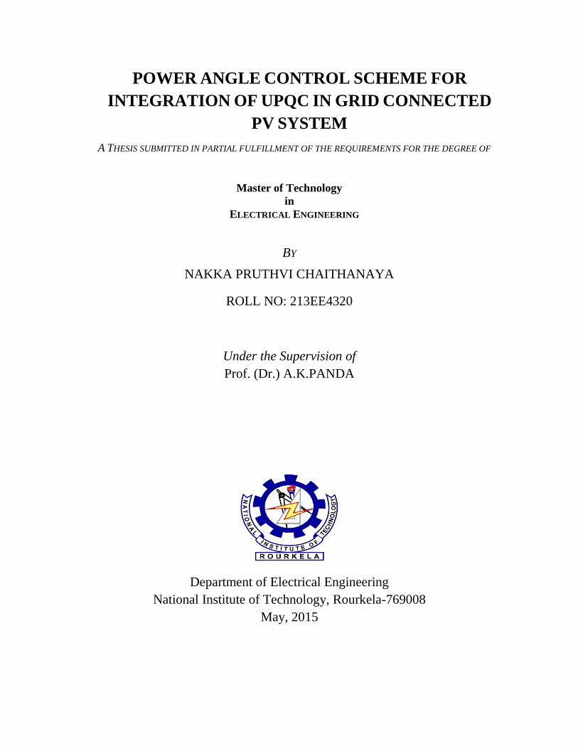
POWER ANGLE CONTROL SCHEME FOR
INTEGRATION OF UPQC IN GRID CONNECTED
PV SYSTEM
A THESIS SUBMITTED IN PARTIAL FULFILLMENT OF THE REQUIREMENTS FOR THE DEGREE OF
Master of Technology
in
ELECTRICAL ENGINEERING
BY
NAKKA PRUTHVI CHAITHANAYA
ROLL NO: 213EE4320
Under the Supervision of
Prof. (Dr.) A.K.PANDA
Department of Electrical Engineering
National Institute of Technology, Rourkela-769008
May, 2015
POWER ANGLE CONTROL SCHEME FOR
INTEGRATION OF UPQC IN GRID CONNECTED
PV SYSTEM
Nakka Pruthvi Chaithanya
Department of Electrical Engineering
National Institute of Technology, Rourkela
Department of Electrical Engineering
National Institute of Technology Rourkela
Certificate
This is to certify that the work in the thesis entitled “POWER ANGLE CONTROL SCHEME
FOR INTEGRATION OF UPQC IN GRID CONNECTED PV SYSTEM” by NAKKA
PRUTHVI CHAITHANYA is a record of an original research work carried out by him
under my supervision and guidance in partial fulfillment of the requirements for the award
of the degree of Master of Technology with the specialization of Power electronics &
Drives in the department of Electrical Engineering, National Institute of Technology
Rourkela. Neither this thesis nor any part of it has been submitted for any degree or
academic award elsewhere.
Place: NIT Rourkela Prof. A . K . P a n d a
Date: May, 2015 Department of Electrical Engineering
National Institute of Technology
Rourkela – 769008
Email: [email protected]

Acknowledgment
First and Foremost, I would like to express my sincere gratitude towards my
supervisor and Head, Department of Electrical Engineering Prof. A. K. Panda, for his
advice during my project work. He has constantly encouraged me to remain focused on
achieving my goal. His observations and comments helped me to establish the overall
direction of the research and to move forward with investigation in depth. He has
helped me greatly and been a source of knowledge.
I am really thankful to PhD scholars especially Shiva Kumar, Sushree Sangita
Patnaik and Nishant Patnaik who helped me during my course work and also in writing
the thesis. Also I would like to thanks my all friends particularly Madhav, Jagan and
Vinay for their personal and moral support. My sincere thanks to everyone who has
provided me with kind words, a welcome ear, new ideas, useful criticism, or their
invaluable time, I am truly indebted.
I must acknowledge the academic resources that I have got from NIT Rourkela. I
would like to thank administrative and technical staff members of the Department who
have been kind enough to advise and help in their respective roles.
Last, but not the least, I would like to acknowledge the love, support and
motivation I received from my parents and therefore I dedicate this thesis to my family.
Nakka Pruthvi Chaithanya
213EE4320
i
Abstract
The quality of electric power is greatly affected by the proliferation of non-linear loads in
electrical energy processing applications like switched mode power supplies, electric motor
drives, battery chargers, etc., The custom power devices like UPQC has gained more importance
in power quality arena as it gives the best solution for all power quality issues. UPQC is the
combination of both shunt and series active power filters connected through a common DC link
capacitor. The shunt active power filter is the most corrective measure to remove the current
related problems, power factor improvement by supplying reactive power and regulates DC link
voltage. The series APF acts as controlled voltage source and corrects voltage related problems,
like sag or swell, flickering, harmonics, etc.,. As a combination of both of these, UPQC improves
service reliability. In the present work, shunt inverter control is based on modified active-
reactive (p-q) power theory, uses High selectivity filter (HSF) for reference current generation.
The series APF uses Power Angle Control (PAC) scheme for compensating sag/swell,
interruption and voltage related problems along with sharing a part of load reactive power
demand with shunt APF and thus ease its loading and makes the utilization of UPQC to be
optimal. The topology uses three phase three leg inverters for both shunt APF and series APF.
The gating signals were generated using Hysteresis controller. The output of High step-Up DC-
DC Converter is used to work as DC voltage source for both APFs. The input voltage for the
converter is provided by Photo Voltaic array incorporated with P&O MPPT technique. The use
of high step-up DC-DC converter is for high voltage gain with better efficiency. The present
topology avoids the PLL in shunt active power filter.
ii
The simulation results are presented to show the effectiveness of the three phase, three-
wire PV-UPQC and here obtained an acceptable THD for source current and kept load voltage at
its nominal value.
iii
CONTENTS PAGE
ABSTRACT………………………………………………………………………………. i
CONTENTS……………………………………………………………………………… iii
LIST OF FIGURES ………………………………………………………………………. v
LIST OF ABBREVATIONS …………………………………………………………….. vii
1. INTRODUCTION ................................................................................................................. 1
1.1 Overview .......................................................................................................................... 1
1.2 Power Quality ................................................................................................................... 3
1.3 Classification of Power Quality Disturbances and their Effects ...................................... 4
1.4 Literature Survey .............................................................................................................. 8
1.5 Motivation ...................................................................................................................... 10
1.6 Objectives ....................................................................................................................... 10
2. CUSTOM POWER DEVICES ............................................................................................ 12
2.1 Custom Power ................................................................................................................ 12
2.2 Custom Power Devices .................................................................................................. 13
2.3 DSTATCOM .................................................................................................................. 13
2.4 DVR ............................................................................................................................... 15
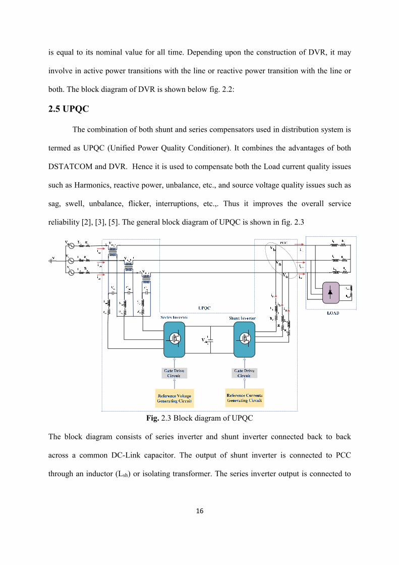
2.5 UPQC ............................................................................................................................. 16
2.6 Summery ........................................................................................................................ 16
3. PHOTO VOLTAIC POWER GENERATING SYSTEM ............................................... 19
3.1 Solar Cell ..................................................................................................................... 20
3.2 P&O MPPT Technique ............................................................................................... 22
3.3 High Step-Up DC-DC Converter…………………………………………………….23
3.4 Summery. ……………………………………………………………………………28
4. PROPOSED CONTROL STRATAGY ............................................................................... 29
4.1 Propose System Description .......................................................................................... 29
4.2 Generation of Reference Voltages for Series APF ......................................................... 30
iv
4.3 Generation of Reference Voltages for Shunt APF ......................................................... 34
4.4 Extracting Fundamental Component using HSF ............................................................ 36
4.5 Gating Signal Generation for Shunt and Series APF ..................................................... 38
4.6 Conclusion…………………………………………………………………………......39
5. SIMULATION RESULTS AND DISCUSSION ................................................................ 40
5.1 For Voltage Sag .............................................................................................................. 41
5.2 For Voltage Swell........................................................................................................... 46
5.3 For Voltage Interruption................................................................................................. 51
5.4 Summery ........................................................................................................................ 58
6. CONCLUSION .................................................................................................................... 59
BIBLIOGRAPHY ................................................................................................................ 60
v
LIST OF FIGURES
Fig. No. Figure Name Page No.
Fig. 1.1 Voltage sag in supply voltage 6
Fig. 1.2 Voltage swell in supply voltage 7
Fig. 2.1 Block diagram of DSTATCOM 13
Fig. 2.2 Block diagram of DVR 14
Fig. 2.3 Block diagram of UPQC 15
Fig. 3.1 Photo Voltaic Cell 19
Fig. 3.2 Flow chart for Perturb and Observe MPPT algorithm 21
Fig. 3.3 High step-up DC-DC converter circuit diagram 22
Fig. 3.4 High step-up dc-dc converter when switch is on 22
Fig. 3.5 High step-up dc-dc converter when switch is off 23
Fig. 3.6 Input voltage applied for high step-up dc-dc converter 24
Fig. 3.7 Output voltage appeared across load for high step-up dc-dc
converter
24
Fig. 4.1 System description block diagram 26
Fig. 4.2 Phasor representation of PAC scheme 28
Fig. 4.3 Reference voltage signal generation block diagram for series
inverter
30
Fig. 4.4 Control block diagram for modified instantaneous p-q Theory 32
Fig. 4.5 Block diagram of HSF 34
vi
Fig. 5.1 Simulation results under voltage sag condition 41
Fig. 5.2 Simulation results under voltage swell condition 46
Fig. 5.3 Simulation results under voltage interruption condition 51
vii
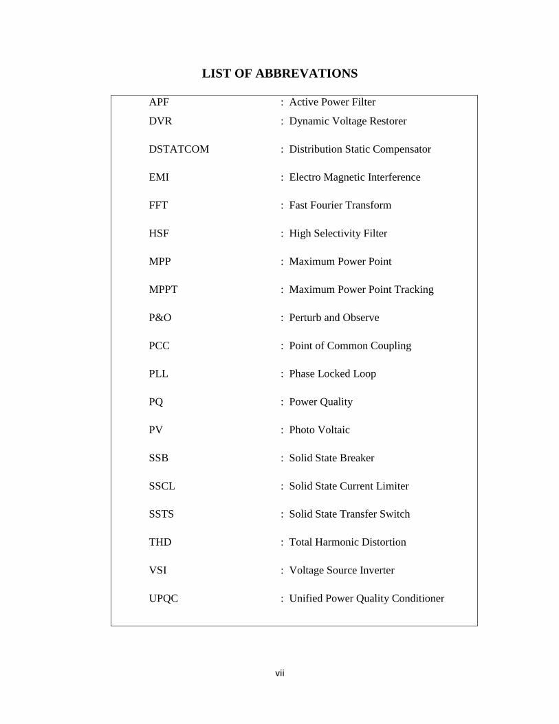
LIST OF ABBREVATIONS
APF : Active Power Filter
DVR : Dynamic Voltage Restorer
DSTATCOM : Distribution Static Compensator
EMI : Electro Magnetic Interference
FFT : Fast Fourier Transform
HSF : High Selectivity Filter
MPP : Maximum Power Point
MPPT : Maximum Power Point Tracking
P&O : Perturb and Observe
PCC : Point of Common Coupling
PLL : Phase Locked Loop
PQ : Power Quality
PV : Photo Voltaic
SSB : Solid State Breaker
SSCL : Solid State Current Limiter
SSTS : Solid State Transfer Switch
THD : Total Harmonic Distortion
VSI : Voltage Source Inverter
UPQC : Unified Power Quality Conditioner
1
CHAPTER 1
INTRODUCTION
1.1 OVERVIEW
The term power quality got significant importance in the electric power industry. The
increasing application of electronic equipment and distributed generation has led to the
degradation of power quality by injecting harmonics, flicker and voltage imbalance into the
system. In addition, switching of capacitor banks, lightning strikes on transmission lines and
various faults on the network also creates the power quality issues such as transients, voltage
sag or swell, interruptions, etc.,.. The equipment which is increasingly susceptible to the
variations in Power Quality is termed as Sensitive Equipment or Sensitive Load [4]. For
proper load operation, it requires pure sinusoidal voltage. With fast growing digital
technology, the devices that depending upon volatile memory chip for storages are increasing
and these are potentially at risk from power quality events.
To achieve this pure sinusoidal voltage and to meet the power quality standards, it is
necessary to use some compensation techniques. Previously passive filters using tuned LC
components have been used to mitigate the harmonics, which are low in cost, simple in
configuration. But this has drawbacks of fixed compensation, bulky in size and creates
resonance problems. Hence a modern solution is found in the form of active power filtering.
The shunt APF is suitable for suppressing source current harmonics and the series APF is
suitable to compensate source voltage imperfections.
The power electronic controllers used in distribution system for the purpose of
supplying a level of reliability or power quality, which is essentially required by sensitive
load, is termed as custom power devices [4]. These devices have the ability to perform
2
voltage regulation and current interruption functions within the distribution system and hence
it can be treated as power conditioning device.
UPQC is one of those efficient custom power devices which is the combination of
both shunt and series active power filters connected through a common DC link capacitor [1],
[2], [6]. The shunt active power filter is the most corrective measure to remove the current
related problems, power factor improvement by supplying reactive power and regulates DC
link voltage [6]. The series APF acts as controlled voltage source [6] and corrects voltage
related problems such as sag/swell, flickering, harmonics etc.,. As a combination of both of
these, UPQC improves service reliability.
In the present work a modified p-q theory is used for reference current generation
shunt APF. It uses two high selectivity filters (HSF) [15], [16], which are used to obtain the
fundamental components from current and voltage signals in �-� reference frame. The fixed
power angle control scheme [2], [5], is used to generate the reference voltage signals for
series APF.
During voltage sag condition the amount of power in UPQC will be increased to a
large extent. The normal UPQC can’t compensate for the long duration power quality issues
as the voltage across DC-Link falls steeply. But the proposed high step-up DC-DC converter
operated PV-UPQC system overcomes this difficulty and able to compensate for long term
voltage interruption, sag/swell, harmonics and reactive power. The additional energy will be
supplied by the PV-array. While interconnecting the PV-UPQC to the grid, the voltage
injected by series APF depends upon the measurement of power angle. As it creates the phase
difference between the source voltage and load voltages, here both active and reactive power
transitions getting involved. Usage of HSF in shunt APF reduces a considerable amount of
THD in source current and avoiding the PLL improves its dynamic response. With the power
3
angle control scheme, series APF shares a part of load reactive power demand along with the
shunt APF. Thus reduces burden and rating of the shunt APF [1], [2], [5].
1.2 POWER QUALITY
A sinusoidal signal of constant amplitude and of single frequency which is constant is
characterized as an ideal voltage or current signal. Further it is required to maintain both
voltage and current in phase. Hence the quality of voltage quality or current quality is the
quality of voltage delivered to the consumer or taken from the utility. Power quality problem
is nothing but the deviation of voltage/current from its ideal value. Though the generator
voltage is at or near pure sinusoidal, the current passing through the load may create
disturbance to it and viz. voltage quality and current quality together is termed as power
quality.
The process of supplying and grounding the sensitive equipment with power such that
the operation of such equipment is satisfactory is nothing but power quality. Power Quality
has different meanings and significances according to the requirement for which it has been
defined. In the perspective of designer or manufacturer, power quality is defined in a manner
that there should be no variation in voltage and no noise generation in the grounding system.
In view of utility engineer, it is voltage availability or outage minutes. For the end users the
feasibility in using the available power for driving all kinds of loads is termed as power
quality.
So a nonstandard voltage, current or frequency that causes maloperation of end user
equipment is termed as power quality problem. Although the entire power system has impact
on power quality, most of the problems occur in distribution system itself. The power quality
became significantly worse at points where the loads are connected to the distribution grid.
4
1.3 CLASSIFICATION OF POWER QUALITY DISTURBANCES AND THEIR
EFFECTS
The presence of the power quality disturbance creates the following effects:
1.3.1 Transients
In power system the term transient is reserved for the occurrence of an unwanted event which
elapses for short duration. Transients are majorly classified in to impulsive and oscillatory
transients.
1.3.1.1 Impulsive transients:
It is a sudden, non-power frequency change in the steady state condition of voltage,
current, or both, which is unidirectional in nature. The rise and delay times characterizes
these transients which can also be obtained by their spectral content.
1.3.1.2 Oscillatory transients:
A sudden, non-power frequency change in the steady state condition of voltage,
current, or both, which extends in both the directions i.e. bidirectional in nature is termed as
oscillatory transient.
Effects:
The following are the undesirable effects caused by the transients.
It causes flashover and damages the equipment. It may lead to insulation failure. It may cause
malfunctioning of electronic equipment.
1.3.2 Voltage Imbalance
It is defined as the ratio of maximum deviation from the average of the three phase
voltages or currents to the average of the three phase voltages or currents, expressed in
percent. Voltage imbalance can be defined making the use of symmetrical components as
well.
5
Effects:
It effects the operation of Induction motors by slowing down and heating it by
creating negative sequence fields.
1.3.3 Waveform Distortion
Waveform distortion is the steady state deviation from an ideal sinusoidal waveform
of power frequency and its characteristics are primarily defined by the spectral content of the
deviation. These are further categorized in to five types. Those are DC Offset, Harmonics,
Inter harmonics, Notching and Noise [4].
1.3.3.1 DC Offset
DC Offset is defined as the existence of a dc voltage or current in an ac power system.
1.3.3.2 Harmonics
The frequency components present in sinusoidal waveforms which are integral multiples of
fundamental frequency can be termed as harmonic components. Distorted waveforms can be
decomposed into a sum of the fundamental frequency and the harmonics. The nonlinear
characteristics of devices and loads on the power system are responsible for the injection of
harmonics in to the system.
Inter Harmonics:
Voltages or currents with frequency components which are non-integral multiples of
the fundamental frequency are said to possess inter harmonics.
Effects:
It causes heating, tripping of controlled process equipment, and equipment failure.
1.3.4 Notching
It is a periodically repeating voltage disturbance occurred due to the presence of
power electronic devices especially during current commutation. The associated frequency
6
components are very high and can’t be characterized with measurement equipment which are
in common use for harmonic analysis.
Effects:
It introduces harmonic and non-harmonic frequencies in the radio frequency range
that cause negative operational effects, such as signal interference introduced into
communication circuits and creates EMI issues.
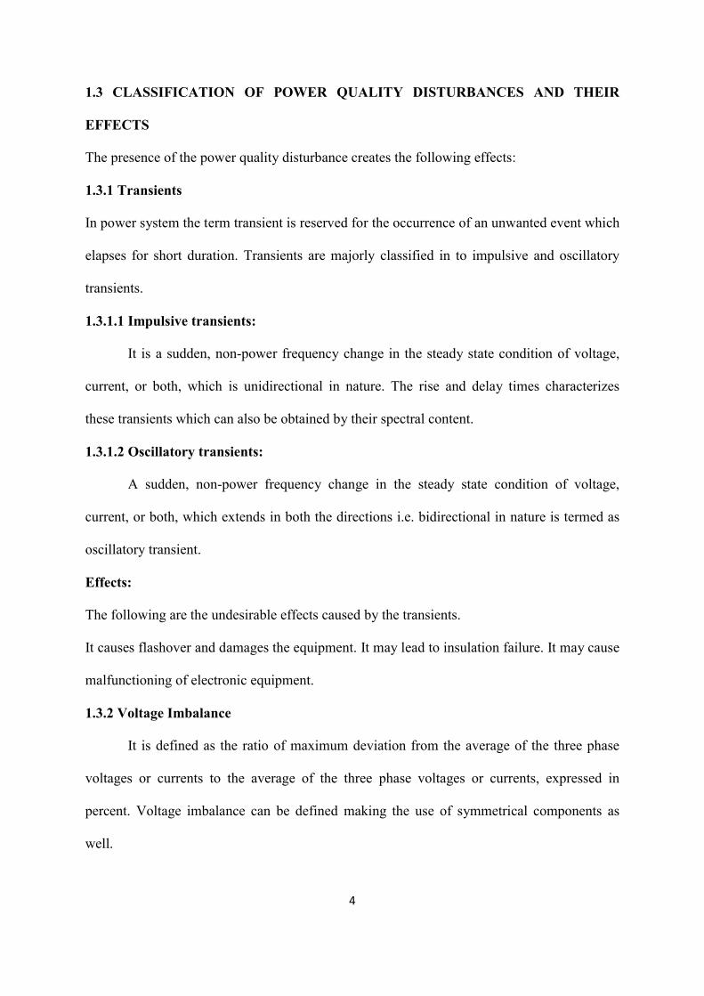
1.3.5 Voltage Sag
Voltage Sag is defined as a decrease in rms voltage at the power frequency for
durations from 0.5 cycles to 1 minute. Voltage sag is a very significant PQ issue for voltage-
sensitive loads such as process control equipment, adjustable speed drives (ASD) and
computers.
0.05 0.1 0.15 0.2 0.25 0.3
-300
-200
-100
0
100
200
300
time in sec
So
urc
e v
olta
ge (
V)
Fig. 1.1 Voltage sag in supply voltage
Voltage sag (dip) is short duration reduction in voltage due to sudden increase of the
current. The most common situations for it are such as transformer energizing, motor starting,
and faults.
Effects:
The major effect of voltage sag includes tripping of relays, malfunctioning of loads,
damage or shut down of the equipment.
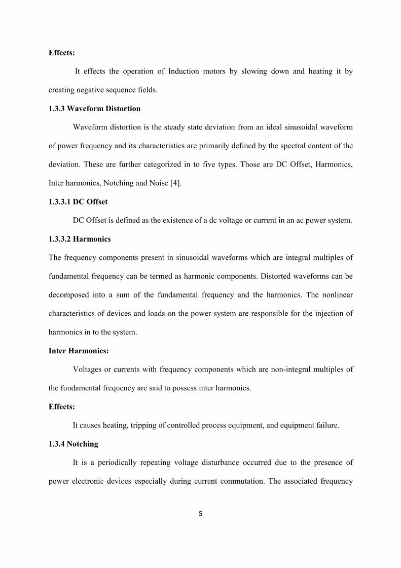
1.3.6 Voltage Swell
It is defined as an increase in the rms supply voltage between 1.1p.u. to 1.8 p.u., and
lasting from half a cycle to 1 min. They are normally appears due to switching off large
7
loads, by energizing capacitor banks, or by faults produced within power system. These are
less probable to appear when compared to voltage sags, but are much more harmful to
sensitive equipment.
0.06 0.08 0.1 0.12 0.14 0.16 0.18 0.2 0.22 0.24 0.26-400
-300
-200
-100
0
100
200
300
400
time in sec
So
urc
e V
olt
age
(V
)
Fig. 1.2 Voltage swell in supply voltage
Effects:
This causes damage or tripping of the equipment which leads to shutdown of whole
process.
1.3.7 Voltage Flicker:
The voltage flicker is a phenomenon of cyclic variation of the voltage waveform
envelope resulting in poor performance of the lighting and other voltage sensitive loads. The
voltage flicker occurs as result of randomly changing reactive power demand of sudden
switching of loads such as arc furnaces, rolling mills, Unbalanced and other fluctuating loads.
Effects:
It causes irritation to human eyes, reduces life span of electronic devices.
1.4 LITERATURE SURVEY
Vinod Khadkikar et al. [1]-[3],[4] presented an overall review on UPQC to improve the
electric power quality at distribution systems and also classified the possible configurations
of UPQCs, its compensation techniques and future scope of each. The author proposed the
PAC approach to improve the utilization factor of series APF.
Basu M et al. [6] presented a series APF that injects voltage at 90° with the supply and
consumes no active power at steady state. It is also shown that the burden of shunt APF is
8
reduced by sharing a part of load reactive power during voltage sag. But it won’t operate
under voltage swell condition.
Mahesh K. Mishra et al. [7] authors have derived mathematical expressions for calculating
various parameters in voltage source inverter configured active power filters used in UPQC
working under unbalanced and distorted conditions.
Ahmed M.A.Haidar et al. discussed the parameters that are affecting the UPQC
performance during voltage sag and harmonic distortion. The authors analyzed the effect of
varying parameters of series APF and shunt APF and calculated THD for both voltage and
current in each case.
Akagi H et al. [14] explained about the physical meaning of instantaneous reactive power
and presented how to generate the reference compensating currents to compensate the
reactive power in three-phase system.
M. Suresh et al. [13] presented the detailed comparison in the performance of instantaneous
p-q and id-iq strategies to generate reference currents of shunt active power filters operating
under distorted and unbalanced conditions. It is proved that id-iq method gives lower THD
under distorted and unbalanced condition.
M.C.Benhabib et al. [15] discussed the three control methods which are based on
instantaneous power theory and the same are compared. The advantages and disadvantages of
each are discussed.
Bhupinder Singh et al. [19] compared the two control techniques, p-q method and id-iq
method, for reference current generation in Shunt APF using PI controller under balanced
condition and showed that the transient response for id-iq method is better than the other.
Hong-seok Song et al. proposed a method to estimate positive and negative sequence
voltages separately for an active power filter operating under voltage sag/swell or unbalanced
condition without any measurement delay.
9
Abdusalam M et al. [23] authors have developed self-tuning filters (STF) based reference
currents generation topology for shunt active power filter control under distorted voltage
conditions
Shahram Karimi et al. [20] presented two high selectivity filters to generate the reference
currents for the positive sequence harmonics, negative sequence harmonics and reactive
power compensation simultaneously without using PLL.
Esram T et al. [17] discussed the different MPPT techniques used to extract the MPP in
photovoltaic (PV) arrays and showed the advantages and disadvantages of each technique
along with estimated cost.
Yi-Ping Hsieh et al. [24] proposed the concept of high step-up boost converter using two
capacitors and one coupled inductor which reduces the stress on main switch and recycles the
stored energy in leakage inductor by using clamping capacitor. The high voltage gain is
obtained by using voltage lift technique.
Fan Ng et al. [9] presented analysis and control algorithm of a three phase four-wire UPQC
based on p-q-r instantaneous power theory.
1.5 MOTIVATION
Several control techniques had developed for improving the PQ using UPQC and
other custom power devices. But still less attention is paid on improving the utilization
factor of series APF which is increasing the rating and cost of UPQC and ability to mitigate
the long term power quality problems such as voltage sag/swell, interruption, harmonics and
reactive power. These became primarily motivation for the current project.
1.6 OBJECTIVES
The objectives of this project include:
To improve the voltage compensation and current compensation capabilities of the
Three-Phase Three-Wire (3P3W) UPQC with power angle control and modified
10
instantaneous active-reactive power (p-q) method using High Selectivity Filters (HSF)
respectively.
To model the perturb and observe MPPT algorithm based and high step-up DC-DC
converter operating Photo Voltaic Power generating system to provide compensation
against long term power quality issues.
1.7 ORGANIZATION OF THESIS
The entire thesis is organized in to six chapters. The explanation in each chapter will
be as follows:
Chapter 1 explains briefly about the introduction to power quality, power quality
disturbances and their effects, literature survey, motivation and objective of the project.
The standard definitions of power quality disturbances and thesis organization also
describe in this chapter.
Chapter 2 describes about what is custom power, the different types of custom power
devices and their functioning. Here it describes the operation of DSTATCOM, DVR and
UPQC. Many different topologies for UPQC like UPQC-P, UPQC-Q , UPQC-VAmin and
UPQC-S are also presented.
Chapter 3 starts with the photo voltaic power generating system followed by modeling of
solar cell, P&O MPPT and high step-up dc-dc converter. The necessity of using high
step-up dc-dc converter along with its functioning is presented. The P&O MPPT
technique is used to control the duty ratio of the high step-up boost converter.
Chapter 4 explains about the complete prosed system description followed by generation
of reference voltages for series APF, reference signal generation for shunt APF and
switching commands generation for both the inverters. This chapter also explains in detail
11
about the PAC approach and advantages. The novelty in the reference signal generation
for shunt APF is due to the usage of HSF and so it is discussed in detail.
Chapter 5 is provided with the MATLAB/SIMULINK simulation results and shows the
effectiveness of proposed PV-UPQC to mitigate the power quality issues. The simulation
results are carried out for voltage sag, swell and interruption cases. The advantages of
using PAC scheme, HSF and P&O MPPT operated high step-up boost converter are
validated.
Chapter 6 gives the conclusion followed by the references.
12
CHAPTER 2
CUSTOM POWER DEVICES
Power quality problems are not very new, traditionally these are mitigated using
passive filters composed of inductors and capacitors. These L and C components are tuned to
suppress specific harmonic frequencies. But these are having many disadvantages, some of
these includes:
These will have fixed range of operation
It introduces resonance into the ac supply
Bulky in size
As time passes by, their impedance value varies.
The effectiveness of its operation depends upon overall system performance and etc.,
The design of notch filter gives best results for a particular harmonic frequency, but in
power system load varies, as much as 0.5Hz is possible. To overcome all these difficulties we
use active power filtering.
2.1 Custom Power
The term custom power indicates the enhanced power quality and reliability which is
delivered to the customers using power electronic controllers. Under this scheme customer
will be free from power interruptions, fluctuations in voltage and current magnitudes,
flickering and Harmonic which may damage to their equipment. In short, it uses power
electronic controllers to keep supply voltage, current and frequency within specified limits.
13
2.2 Custom Power Devices
The power electronic devices, which are connected in series or in shunt or a
combination of both [4] to enhance the power quality, are called Custom Power Devices.
These are broadly classified into two types
i. Network reconfiguring devices and
ii. Compensating devices.
The network reconfiguring devices are used either to limit or to break or to transfer the
current, which are usually called switch gear. The solid state or static versions of the devices
are called Solid state current limiter (SSCL), Solid state breaker (SSB) and Solid state
transfer switch (SSTS).
The compensating devices are either used to improve the quality of voltage i.e., sag,
swell, flickering, etc., or to improve the quality of current, or both by injecting compensating
voltage or current or both respectively. These devices include:
a) Distribution STATCOM (DSTATCOM)
b) Dynamic Voltage Restorer (DVR)
c) Unified Power Quality Conditioner (UPQC)
2.3 DSTATCOM
The shunt compensating device in distribution system is termed as DSTATCOM. It
acts as controlled current source to mitigate the load harmonics. The main intention of
connecting the shunt compensating device is to
provide harmonic isolation between the load and source
provide load VAR compensation and to operate source nearly at unity power factor
suppress the dc offset in loads such that source current offset is eliminated
balance the source current even if the load is unbalanced
14
maintain voltage across the DC-Link capacitor to a reference value in VSI mode.
The block diagram of DSTATCOM is shown in below fig. 2.1
Fig. 2.1 Block diagram of DSTATCOM
The circuit is realized by an inverter, Inductor filters, DC source (usually capacitor),
control circuit to generate reference currents, gate drive circuits for inverter switches. The
capacitor acts as DC source and inverter is used to convert the DC input into AC output and
is connected to PCC and injects current through an inductor or transformer. The PCC refers
to the location in the network where other customers may be connected. Hence the voltage
distortion at PCC is limited from the view point of safety to customer’s equipment. The
important aspect in its operation is that the injected currents should track the reference
15
currents. For that, the control circuit with appropriate reference current generating techniques
will be used. The gate drive circuit operates the switches accordingly and inverter tracks the
reference currents. And thus the harmonic currents will be compensated.
2.4 DVR
Fig. 2.2 Block diagram of DVR
The DVR is nothing but a series compensating device in distribution system. It acts as
controlled voltage source. It is used to regulate the supply voltage quality and maintains the
voltage at PCC to be insensitive to the supply voltage problems such as sag, swell, flickering,
unbalance, interruptions, and other supply voltage disturbances. It injects the compensating
voltage between supply and load in such a way that the terminal voltage or voltage at its PCC
16
is equal to its nominal value for all time. Depending upon the construction of DVR, it may
involve in active power transitions with the line or reactive power transition with the line or
both. The block diagram of DVR is shown below fig. 2.2:
2.5 UPQC
The combination of both shunt and series compensators used in distribution system is
termed as UPQC (Unified Power Quality Conditioner). It combines the advantages of both
DSTATCOM and DVR. Hence it is used to compensate both the Load current quality issues
such as Harmonics, reactive power, unbalance, etc., and source voltage quality issues such as
sag, swell, unbalance, flicker, interruptions, etc.,. Thus it improves the overall service
reliability [2], [3], [5]. The general block diagram of UPQC is shown in fig. 2.3
Fig. 2.3 Block diagram of UPQC
The block diagram consists of series inverter and shunt inverter connected back to back
across a common DC-Link capacitor. The output of shunt inverter is connected to PCC
through an inductor (Lsh) or isolating transformer. The series inverter output is connected to
17
the injection transformers through a Low pass filter formed by Lse and Cse circuit. The
operation of series APF is same as DVR and of shunt APF is same as DSTATCOM.
The shunt inductor is used for smoothening the current harmonics and also an
interface between shunt inverter and PCC. The series LPF is used to inject only lower order
harmonics in to the line. It also helps to provide isolation between the line and series inverter.
The shunt inverter regulates the DC voltage across capacitor using a feedback controller
which is tuned in such a way that its value remains fixed at set reference value under dynamic
conditions with minimum over shoot and settling time.
2.5.1 TYPES OF UPQC
2.5.1.1 Classification based on the Physical Structure
Different UPQC topologies are utilized such as two, three phase three-leg (3P3L)
VSIs with split capacitor, a three-phase three-Leg (3P3L) VSI for shunt APF and three-phase
four leg(3P4L) VSI topology for series and two three phase- phase four-leg (3P4L) VSI
topology for enhancing power quality in a three phase four wire system. For three phase three
wire system (3P3W) it usually uses three two three phase three- leg VSIs. For single phase
UPQC, the VSI may be based on two H-bridge inverters or half bridge inverters or single
phase three-leg topology.
2.5.1.2 Classification based on UPQC system to compensate the voltage sag
The four existing methods to compensate voltage sag in literature are as follows:
a) UPQC-P: In this method, the injected voltage, which is equal to the reduced
magnitude of nominal voltage at PCC, will be in series with the line, which involves
injection of active power in to the line [1], [5]. In conventional UPQC, the shunt APF
draws the required active power to be injected by the series APF and the losses
18
occurred in shunt APF from supply, which increases the source current magnitude
during voltage sag.
b) UPQC-Q: In this method the series voltage is injected in quadrature with the load
voltage such that the voltage at PCC is equal to the rated voltage. Thus the voltage sag
is mitigated by injecting the reactive power in to the system. Hence it is called UPQC-
Q [6] method. The shunt APF maintains the source power factor at unity, which
avoids the requirement of active power to compensate the voltage sag.
Here the resultant voltage achieved is greater than the voltage injected in UPQC-P for
same percentage of voltage sag. Hence the rating of UPQC will be increased. Another
disadvantage of UPQC-Q is its inability to compensate the voltage swell.
c) UPQC-VAmin: If the injected voltage is neither in series nor in quadrature with load
voltage but makes an optimal angle with the source current such that the loading of
UPQC will be min during the voltage sag condition is termed as UPQC-VAmin
method [1], [2], [5]. Another advantage of this method is that, at steady state, both
shunt APF and series APF will supply the load reactive power demand, which reduces
the rating of shunt APF.
d) UPQC-S: This method is similar to UPQC-VAmin, but the change is that the series
APF is used to load up to its rated value. Thus the series APF delivers both active and
reactive power [1]-[3], [5].
2.6 SUMMARY
The poor Power Quality causes a huge financial losses and inconvenience to the end users.
To avoid this and to improve the reliability, the need of custom power distribution has arisen.
Custom power devices are static power electronic controllers, includes DVR, DSTATCOM
and UPQC with different topologies used to eliminate the power quality issues in distribution
system. These will improve the service reliability and allows end users equipment to operate

19
in an appropriate manner by mitigating voltage issues or current issues or both. In this chapter
types of custom power devices, different possible topologies and their circuit configurations
are discussed.
The next chapter explains about the photo voltaic power generating system using high
step-up dc-dc converter and P&O MPPT technique.
20
CHAPTER 3
PHOTO VOLTAIC POWER GENERATING SYSTEM
Photo voltaic power generation uses solar cells to convert solar irradiation into
electrical energy. A grid connected PV system converts light energy into electrical energy
directly and thus it mainly reduces the energy extracted from the electrical utility. The
development in power electronics and material science has helped to develop compact but
efficient systems to withstand the high power demand. The PV cell exhibits nonlinear I–V
and P–V characteristics. The series connected solar cells, which are basic building blocks of
it, forms a PV module. These PV modules are connected either in series or in parallel
depending upon its power rating forms a PV array. The maximum power produced varies
with temperature and irradiance. Each cell has different current and voltage maximum
positions as these have non-linear characteristics. But the power maximum point is unique,
which mainly depends upon Temperature and Irradiation. To track that maximum power
point, it is essential to use MPPT algorithm.
The maximum power point tracking (MPPT) algorithm is used to extract the
maximum power from PV panels from instantaneous variations of irradiation, temperature
and PV module characteristics.
3.1 SOLAR CELL
The PV array model is developed by the basic equations of photovoltaic cells,
including the effects of temperature changes and solar irradiation level. Each cell is capable
of producing 0.5- 2Volts. And here it is modeled to give 36V as its output using P&O MPPT,
which acts as input to dc-dc boost converter.
21
Iph
ID
Rsh
Rse
D
IPV ISH
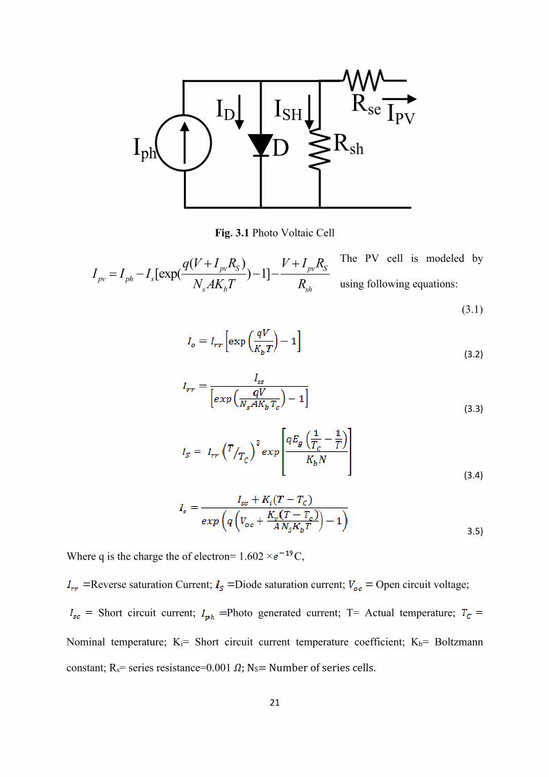
Fig. 3.1 Photo Voltaic Cell
The PV cell is modeled by
using following equations:
(3.1)
(3.2)
(3.3)
(3.4)
3.5)
Where q is the charge the of electron= 1.602 × C,
Reverse saturation Current; Diode saturation current; Open circuit voltage;
Short circuit current; Photo generated current; T= Actual temperature;
Nominal temperature; Ki= Short circuit current temperature coefficient; Kb= Boltzmann
constant; Rs= series resistance=0.001 �; NS= Number of series cells.
( )[exp( ) 1]pv S pv S
pv ph s
s b sh
q V I R V I RI I I
N AK T R
22
3.2 P&O MPPT TECHNIQUE
Maximum Power Point Tracking technique uses maximum power transfer theorem,
which states that, the output power is maximum when thevinins impedance of circuit is equal
to the load impedance. Hence tracking the maximum power point is nothing but tracking the
impedance matching point. There are many MPPT techniques available like perturb and
observe technique, Perturb and Observe (P&O), Incremental Conductance method, Neural
networks method, Fractional open circuit voltage method, Fractional short circuit current
method, Fuzzy logic method [17], etc.,. The suitability of technique depends on different
parameters like cost, application, dynamic performance and ease of implementation. Here we
considered P&O MPPT technique for our application. The P&O MPPT uses only one voltage
sensor. Hence it is cost effective and easy to implement.
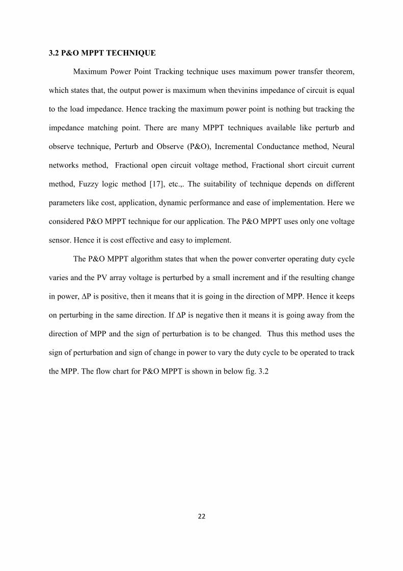
The P&O MPPT algorithm states that when the power converter operating duty cycle
varies and the PV array voltage is perturbed by a small increment and if the resulting change
in power, ∆P is positive, then it means that it is going in the direction of MPP. Hence it keeps
on perturbing in the same direction. If ∆P is negative then it means it is going away from the
direction of MPP and the sign of perturbation is to be changed. Thus this method uses the
sign of perturbation and sign of change in power to vary the duty cycle to be operated to track
the MPP. The flow chart for P&O MPPT is shown in below fig. 3.2
23
Fig. 3.2 Flow chart for Perturb and Observe MPPT algorithm
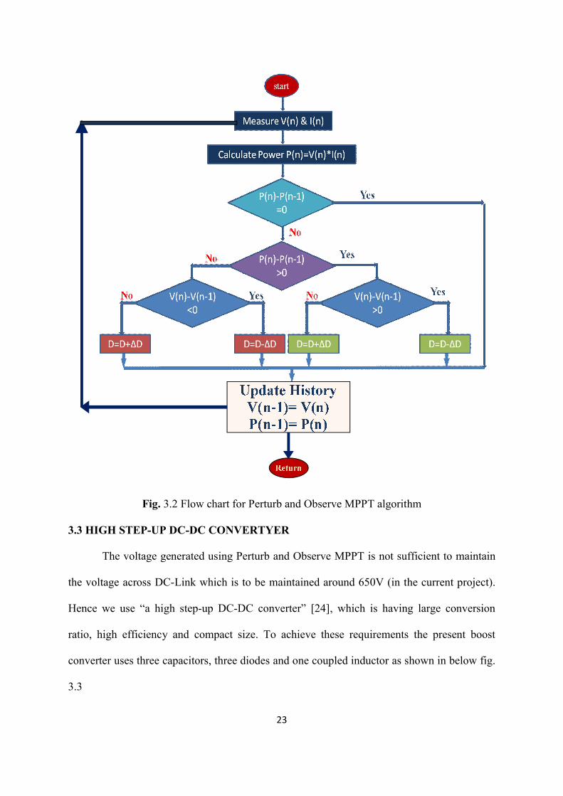
3.3 HIGH STEP-UP DC-DC CONVERTYER
The voltage generated using Perturb and Observe MPPT is not sufficient to maintain
the voltage across DC-Link which is to be maintained around 650V (in the current project).
Hence we use “a high step-up DC-DC converter” [24], which is having large conversion
ratio, high efficiency and compact size. To achieve these requirements the present boost
converter uses three capacitors, three diodes and one coupled inductor as shown in below fig.
3.3
24
Fig. 3.3 High step-up DC-DC converter circuit diagram
The circuit consists of:
DC input voltage Vin, MOSFET switch SW, coupled inductors Np and Ns, one clamp diode
D1, clamp capacitor C1, two capacitors C2 and C3, two diodes D2 and D3, output diode Do, and
output capacitor Co, magnetizing inductor Lm, leakage inductor Lk, and an ideal transformer.
The capacitor C1 is used to recycle the energy stored by the Leakage inductor (Lk). Thus it
clamps the voltage across switch, SW to a lower value which reduces the voltage stress on
the switch. The CCM operation of the converter is explained below:
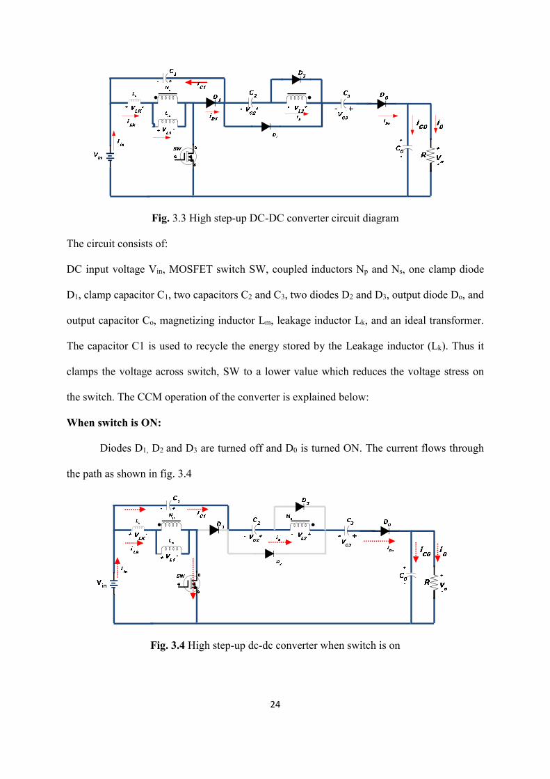
When switch is ON:
Diodes D1, D2 and D3 are turned off and D0 is turned ON. The current flows through
the path as shown in fig. 3.4
Fig. 3.4 High step-up dc-dc converter when switch is on
25
The magnetizing inductor stores the energy developed by the input source voltage, Vin. The
same energy is transferred to the secondary side of the coupled inductor. Thus the voltages
Vin, VC1, VC2 and VC3 will be connected in series and it discharges the energy to the capacitor
C0 and load R. The output voltage is given by
(3.6)
When switch is OFF:
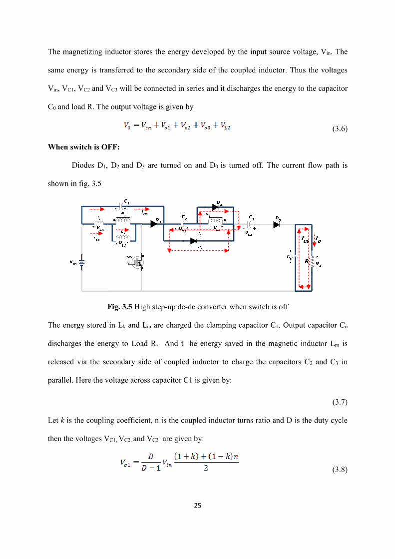
Diodes D1, D2 and D3 are turned on and D0 is turned off. The current flow path is
shown in fig. 3.5
Fig. 3.5 High step-up dc-dc converter when switch is off
The energy stored in Lk and Lm are charged the clamping capacitor C1. Output capacitor Co
discharges the energy to Load R. And t he energy saved in the magnetic inductor Lm is
released via the secondary side of coupled inductor to charge the capacitors C2 and C3 in
parallel. Here the voltage across capacitor C1 is given by:
(3.7)
Let k is the coupling coefficient, n is the coupled inductor turns ratio and D is the duty cycle
then the voltages VC1, VC2, and VC3 are given by:
(3.8)
26
(3.9)
(3.10)
Where VC1, VC2, and VL2 are voltage across capacitors and is the voltage across inductor
respectively. Substituting the above equations gives the voltage gain as
(3.11)
At k=1,
(3.12)
The major role of this converter is to maintain constant voltage across the DC-Link of
the two inverters by operating itself at the duty ratio of obtaining MPP of PV array. This duty
ratio is obtained by Perturb and Observe MPPT algorithm.
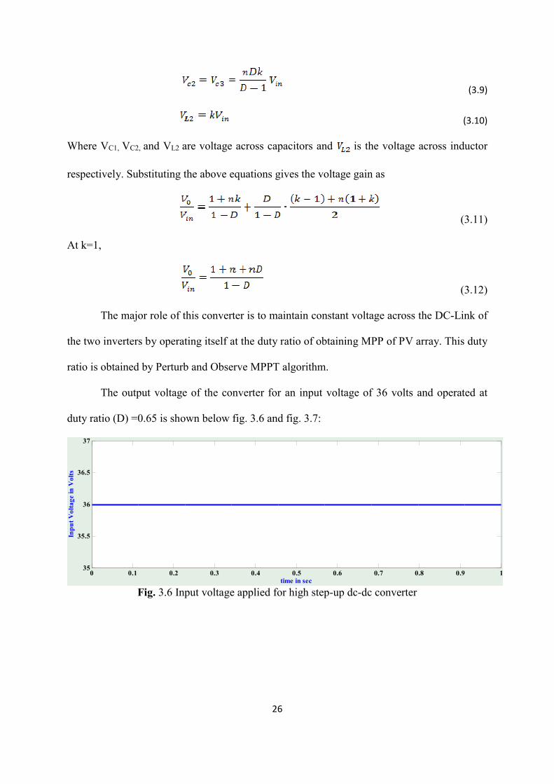
The output voltage of the converter for an input voltage of 36 volts and operated at
duty ratio (D) =0.65 is shown below fig. 3.6 and fig. 3.7:
0 0.1 0.2 0.3 0.4 0.5 0.6 0.7 0.8 0.9 135
35.5
36
36.5
37
time in sec
Inp
ut
Vo
ltag
e in
Vo
lts
Fig. 3.6 Input voltage applied for high step-up dc-dc converter
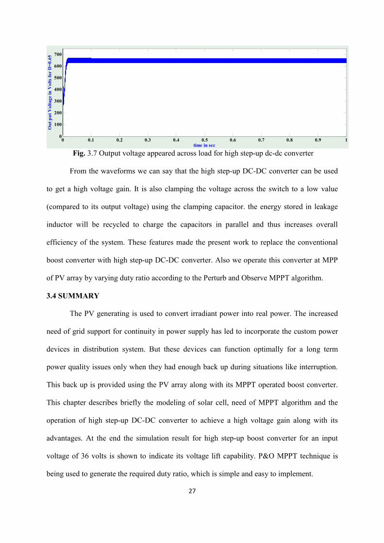
27
0 0.1 0.2 0.3 0.4 0.5 0.6 0.7 0.8 0.9 10
100
200
300
400
500
600
700
time in sec
Ou
t p
ut
Vo
ltag
e in
Vo
lts
for
D=
0.6
5
Fig. 3.7 Output voltage appeared across load for high step-up dc-dc converter
From the waveforms we can say that the high step-up DC-DC converter can be used
to get a high voltage gain. It is also clamping the voltage across the switch to a low value
(compared to its output voltage) using the clamping capacitor. the energy stored in leakage
inductor will be recycled to charge the capacitors in parallel and thus increases overall
efficiency of the system. These features made the present work to replace the conventional
boost converter with high step-up DC-DC converter. Also we operate this converter at MPP
of PV array by varying duty ratio according to the Perturb and Observe MPPT algorithm.
3.4 SUMMARY
The PV generating is used to convert irradiant power into real power. The increased
need of grid support for continuity in power supply has led to incorporate the custom power
devices in distribution system. But these devices can function optimally for a long term
power quality issues only when they had enough back up during situations like interruption.
This back up is provided using the PV array along with its MPPT operated boost converter.
This chapter describes briefly the modeling of solar cell, need of MPPT algorithm and the
operation of high step-up DC-DC converter to achieve a high voltage gain along with its
advantages. At the end the simulation result for high step-up boost converter for an input
voltage of 36 volts is shown to indicate its voltage lift capability. P&O MPPT technique is
being used to generate the required duty ratio, which is simple and easy to implement.
28
CHAPTER 4
PROPOSED CONTROL STRATAGY
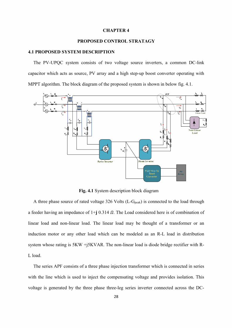
4.1 PROPOSED SYSTEM DESCRIPTION
The PV-UPQC system consists of two voltage source inverters, a common DC-link
capacitor which acts as source, PV array and a high step-up boost converter operating with
MPPT algorithm. The block diagram of the proposed system is shown in below fig. 4.1.
Linear Load
Non-Linear Load
Fig. 4.1 System description block diagram
A three phase source of rated voltage 326 Volts (L-Gpeak) is connected to the load through
a feeder having an impedance of 1+j 0.314 �. The Load considered here is of combination of
linear load and non-linear load. The linear load may be thought of a transformer or an
induction motor or any other load which can be modeled as an R-L load in distribution
system whose rating is 5KW +j5KVAR. The non-linear load is diode bridge rectifier with R-
L load.
The series APF consists of a three phase injection transformer which is connected in series
with the line which is used to inject the compensating voltage and provides isolation. This
voltage is generated by the three phase three-leg series inverter connected across the DC-
29
Link. The series inverter is connected to the series injection transformer through an LPF
formed by Rse, Lse and Cse, whose purpose is to remove distortions resulted by switching of
inverter. The shunt APF is used to inject the current at PCC through the inductor filter to
mitigate the current harmonics and to maintain a constant voltage across the DC-Link.
The PV array is connected to the grid through the UPQC. It uses the high step-up DC-DC
converter whose operating duty ratio is generated by Perturb and Observe MPPT algorithm.
The output of this high step-up boost converter is connected across the dc-link, whose voltage
remains constant.
4.2 GENERATION OF REFERENCE VOLTAGES FOR SERIES APF
The generation of reference voltages for series APF is based on the power angle
control scheme. The brief explanation and advantages of the scheme is explained in the
following section.
4.2.1 POWER ANGLE CONTROL SCHEME
The rating of series APF used in UPQC depends upon the maximum percentage of sag/swell
that it should compensate. But these are of small duration issues. But the shunt APF operates
as long as the non-linear currents are drawn from the source. It supplies the reactive power
continuously, which leads to increased utilization of it compared to series APF. The power
angle control scheme is mainly used to increase the utilization factor of series APF without
causing any additional burden on it. Here the series APF is used to share a part of load
reactive power demand along with compensating voltage sag/swell by creating a power angle
difference between source voltage and load voltage.
The compensation of sag can be done by active power approach or reactive approach or by
both of these in UPQC. Here this scheme uses both active and reactive power approach to
compensate the sag/swell by maintaining a constant load voltage. The operation is better
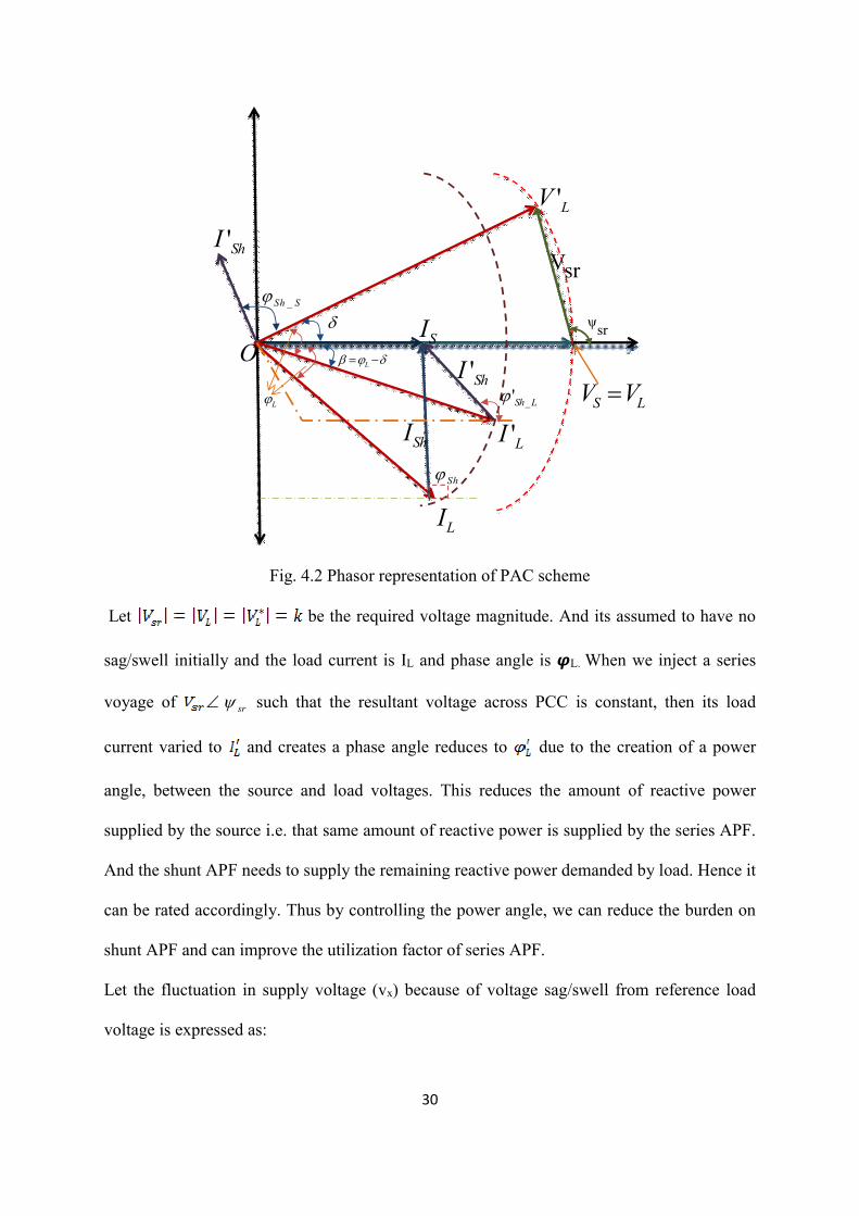
explained using the phasor diagram shown in below fig. 4.2
30
O
LI
'LV
'ShI
'LI
'ShI
SI
ShI
S LV V
L
Sh
_Sh S
L _'Sh L
srV
srψ
Fig. 4.2 Phasor representation of PAC scheme
Let be the required voltage magnitude. And its assumed to have no
sag/swell initially and the load current is IL and phase angle is �L. When we inject a series
voyage of sr such that the resultant voltage across PCC is constant, then its load
current varied to and creates a phase angle reduces to due to the creation of a power
angle, between the source and load voltages. This reduces the amount of reactive power
supplied by the source i.e. that same amount of reactive power is supplied by the series APF.
And the shunt APF needs to supply the remaining reactive power demanded by load. Hence it
can be rated accordingly. Thus by controlling the power angle, we can reduce the burden on
shunt APF and can improve the utilization factor of series APF.
Let the fluctuation in supply voltage (vx) because of voltage sag/swell from reference load
voltage is expressed as:
31
*
*
L
Lsf
V
VVk
, where Kf is the fluctuation factor (4.1)
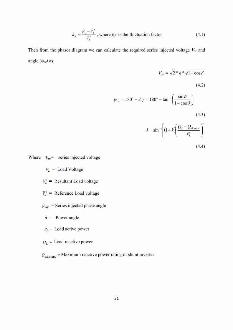
Then from the phasor diagram we can calculate the required series injected voltage Vsr and
angle (ψsr) as:
cos1**2 kVsr
(4.2)
cos1
sintan180180 1
sr
(4.3)
L
shL
P
QQk max,1 1sin
(4.4)
Where = series injected voltage
Load Voltage
Resultant Load voltage
Reference Load voltage
sr = Series injected phase angle
� = Power angle
LP Load active power
LQ Load reactive power
max,shQ Maximum reactive power rating of shunt inverter
32
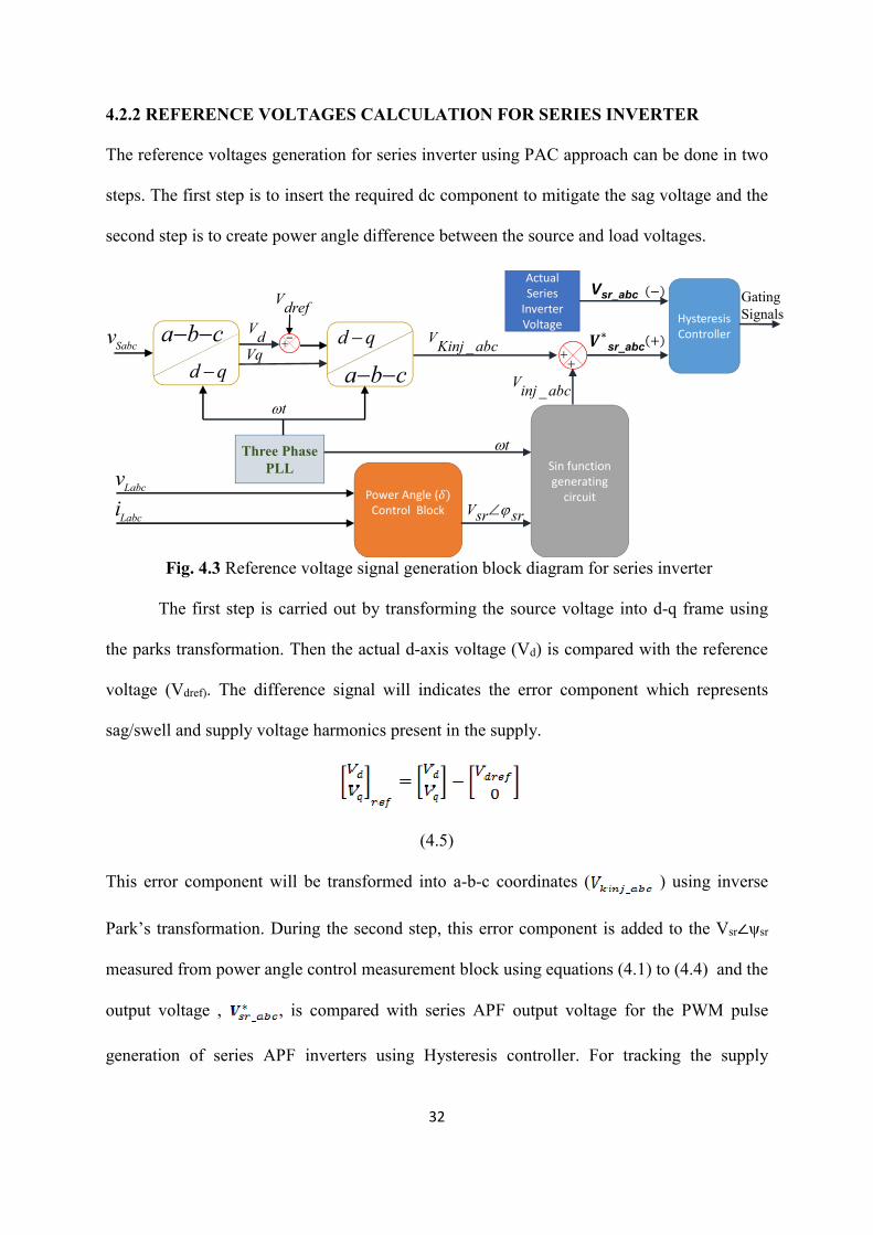
4.2.2 REFERENCE VOLTAGES CALCULATION FOR SERIES INVERTER
The reference voltages generation for series inverter using PAC approach can be done in two
steps. The first step is to insert the required dc component to mitigate the sag voltage and the
second step is to create power angle difference between the source and load voltages.
Three PhasePLL
cba
qd
Sabcv d
V
drefV
cba
qd
Power Angle (�)Control Block
Labcv
Labci
abcinjV
_
srsrV
VqabcKinj
V_
t
t
sr_abc
Hysteresis Controller
Actual Series
Inverter Voltage
Vsr_abc Gating Signals
Sin function generating
circuit
Fig. 4.3 Reference voltage signal generation block diagram for series inverter
The first step is carried out by transforming the source voltage into d-q frame using
the parks transformation. Then the actual d-axis voltage (Vd) is compared with the reference
voltage (Vdref). The difference signal will indicates the error component which represents
sag/swell and supply voltage harmonics present in the supply.
(4.5)
This error component will be transformed into a-b-c coordinates ( ) using inverse
Park’s transformation. During the second step, this error component is added to the Vsr∠ψsr
measured from power angle control measurement block using equations (4.1) to (4.4) and the
output voltage , , is compared with series APF output voltage for the PWM pulse
generation of series APF inverters using Hysteresis controller. For tracking the supply
33
frequency it uses PLL. The complete approach is summarized in the block diagram shown in
fig. 4.3.
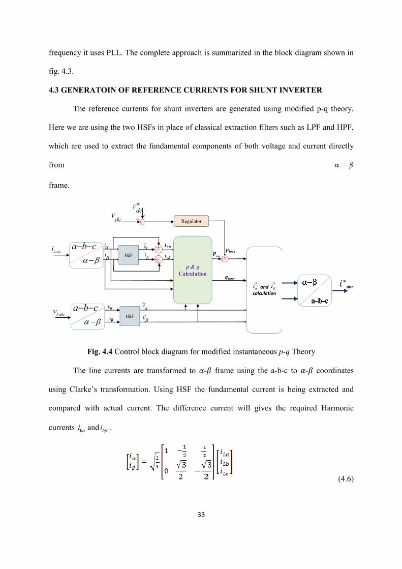
4.3 GENERATOIN OF REFERENCE CURRENTS FOR SHUNT INVERTER
The reference currents for shunt inverters are generated using modified p-q theory.
Here we are using the two HSFs in place of classical extraction filters such as LPF and HPF,
which are used to extract the fundamental components of both voltage and current directly
from
frame.
Regulator
*i
*dc
V
HSF
v~v
~
cba
i~
i~Labc
i
Labcv cba
HSF
p & qCalculation
qtotal
*iand
calculation
i
i
dcV
abc
Fig. 4.4 Control block diagram for modified instantaneous p-q Theory
The line currents are transformed to �-� frame using the a-b-c to �-� coordinates
using Clarke’s transformation. Using HSF the fundamental current is being extracted and
compared with actual current. The difference current will gives the required Harmonic
currents hi and hi .
(4.6)
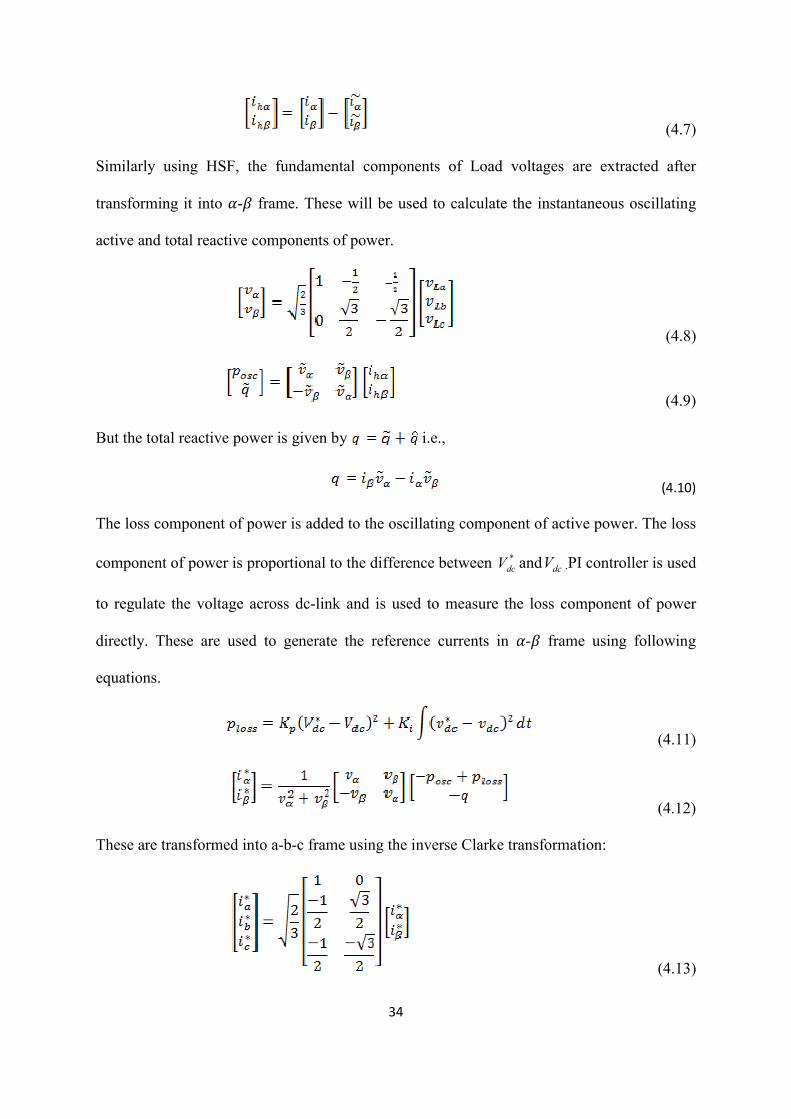
34
(4.7)
Similarly using HSF, the fundamental components of Load voltages are extracted after
transforming it into �-� frame. These will be used to calculate the instantaneous oscillating
active and total reactive components of power.
(4.8)
(4.9)
But the total reactive power is given by i.e.,
(4.10)
The loss component of power is added to the oscillating component of active power. The loss
component of power is proportional to the difference between *dcV and dcV .PI controller is used
to regulate the voltage across dc-link and is used to measure the loss component of power
directly. These are used to generate the reference currents in �-� frame using following
equations.
(4.11)
(4.12)
These are transformed into a-b-c frame using the inverse Clarke transformation:
(4.13)
35
The measured currents are compared with actual shunt APF currents in order to generate the
gating signals for shunt inverter using Hysteresis controller. The corresponding block
diagram is shown in fig. 4.4.
4.4 EXTRACTING FUNDAMENTAL COMPONENT USING HSF
The performance of modified instantaneous active- reactive power method depends
upon how accurately we generate the harmonic currents in reference current generation. This
mainly depends upon the Filter we used to extract the fundamental. The conventional LPF
and HPF had lower bandwidth and hence create a measurement delay. And this creates a
sluggish response which should be avoided to protect the sensitive equipment. This problem
can be alleviated by using the High Selectivity Filter (HSF) as it suppresses the negative
sequence field produced by unbalance or distortion in the signal. And it allows only
fundamental component, which is selected as its cut-off frequency to pass through it in
frame. The other advantages of the HSF includes: operates effectively in transient state and
offers unity gain at the fundamental frequency.
The integration in the synchronous reference frame is defined for an instantaneous
signal is given by:
(4.14)
The transfer function of the system can be expressed as:
(4.15)
Here a constant K is introduced in the transfer function H(s), to obtain a cutoff frequency ωc
in the HSF. Now, the new transfer function is:
(4.16)
36
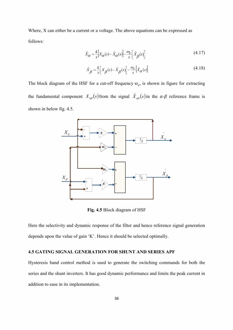
Where, X can either be a current or a voltage. The above equations can be expressed as
follows:
sXscsXsX
sk
X
ˆˆˆ
(4.17)
sXscsXsX
sk
X
ˆˆˆ
(4.18)
The block diagram of the HSF for a cut-off frequency , is shown in figure for extracting
the fundamental component sX from the signal sXˆ in the �-� reference frame is
shown in below fig. 4.5.
K
wc
K
+
_
+
_
S1
-
+
-
+
^
X
^
X
X
X
wc
S1
Fig. 4.5 Block diagram of HSF
Here the selectivity and dynamic response of the filter and hence reference signal generation
depends upon the value of gain ‘K’. Hence it should be selected optimally.
4.5 GATING SIGNAL GENERATION FOR SHUNT AND SERIES APF
Hysteresis band control method is used to generate the switching commands for both the
series and the shunt inverters. It has good dynamic performance and limits the peak current in
addition to ease in its implementation.
37
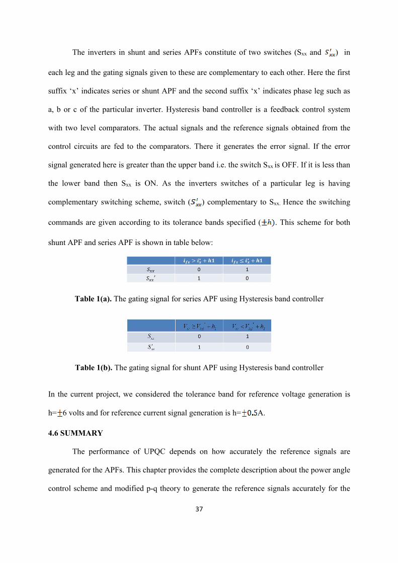
The inverters in shunt and series APFs constitute of two switches (Sxx and ) in
each leg and the gating signals given to these are complementary to each other. Here the first
suffix ‘x’ indicates series or shunt APF and the second suffix ‘x’ indicates phase leg such as
a, b or c of the particular inverter. Hysteresis band controller is a feedback control system
with two level comparators. The actual signals and the reference signals obtained from the
control circuits are fed to the comparators. There it generates the error signal. If the error
signal generated here is greater than the upper band i.e. the switch Sxx is OFF. If it is less than
the lower band then Sxx is ON. As the inverters switches of a particular leg is having
complementary switching scheme, switch ( ) complementary to Sxx. Hence the switching
commands are given according to its tolerance bands specified ( . This scheme for both
shunt APF and series APF is shown in table below:
Table 1(a). The gating signal for series APF using Hysteresis band controller
Table 1(b). The gating signal for shunt APF using Hysteresis band controller
In the current project, we considered the tolerance band for reference voltage generation is
h= 6 volts and for reference current signal generation is h= A.
4.6 SUMMARY
The performance of UPQC depends on how accurately the reference signals are
generated for the APFs. This chapter provides the complete description about the power angle
control scheme and modified p-q theory to generate the reference signals accurately for the
38
series and shunt APFs respectively. It also describes how the PAC approach is useful to
reduce the cost and the burden on shunt APF. To increase the performance of shunt APF the
conventional filters are replaced by HSF in shunt APF. This HSF is used to reduce the
harmonic distortion in the line to a great extent. The dynamic performance of system is
improved by using the Hysteresis controller for generating the switch commands to the
inverters with suitable hysteresis band selection.
Next chapter presents the information about system parameters selected for the
current project and presents the simulation results carried out to show the performance of the
proposed system.
39
CHAPTER 5
SIMULATION RESULTS AND DISCUSSION
The simulation results are carried out by considering both Linear and Non-Linear Loads. The
PV-UPQC system parameters are rated as below:
Source: System Voltage (L-G) = 326V
System Frequency, f= 50 Hz
Load: ` Linear Load of rating= 5KW +j5KVAR and
Non-Linear Load: Diode bridge rectifier with R-L load;
where RL=30� and LL=1mH.
Feeder: Impedance = 1+j 0.314 �
The Series APF parameters: Rse=0.6; Lse=4.2 mH; Cse= 60μF;
Injection transformer rating: 1∶1, 120 Volts
The Shunt APF parameters: Lf = 2.5 mH; and Rf = 5m�;
DC Link Capacitor, Cdc =2200μF;
DC-Link Voltage, Vdc= 650 V;
PI Controller: Kp= 0.1; and KI= 20;
PV Array: No. of series cells= 6 8,
Voltage at MPP= 36Volts,
Current at MPP= 7Amps,
Nominal voltage= 12Vots;
High Step-Up DC-DC Converter: DC input voltage = 36 V
Output Voltage = 650V
Capacitors C1= 56μF, C2=C3= 22μF and C0 = 180μF;
Np∶Ns = 1∶4, Lm =48μH;
40
Switching frequency = 50 KHz;
The initial Load power factor of load = 0.837
The proposed PV-UPQC is evaluated using MATLAB/Simulink software for voltage Sag,
Swell and Interruption and the simulation results are given below.
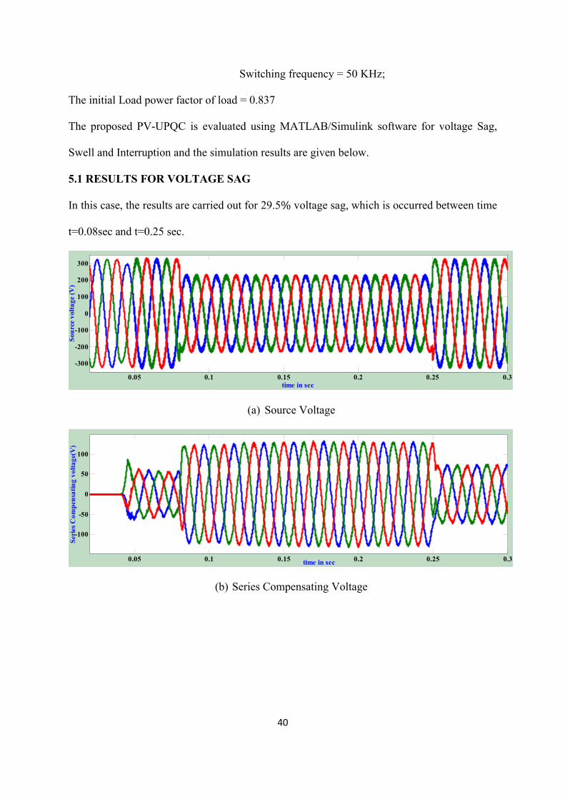
5.1 RESULTS FOR VOLTAGE SAG
In this case, the results are carried out for 29.5% voltage sag, which is occurred between time
t=0.08sec and t=0.25 sec.
0.05 0.1 0.15 0.2 0.25 0.3
-300
-200
-100
0
100
200
300
time in sec
Sou
rce
vol
tag
e (V
)
(a) Source Voltage
0.05 0.1 0.15 0.2 0.25 0.3
-100
-50
0
50
100
time in sec
Ser
ies
Co
mp
ensa
tin
g v
olt
ag
e(V
)
(b) Series Compensating Voltage
41
0.05 0.1 0.15 0.2 0.25 0.3
-300
-200
-100
0
100
200
300
time in sec
Vo
lta
ge
at
PC
C
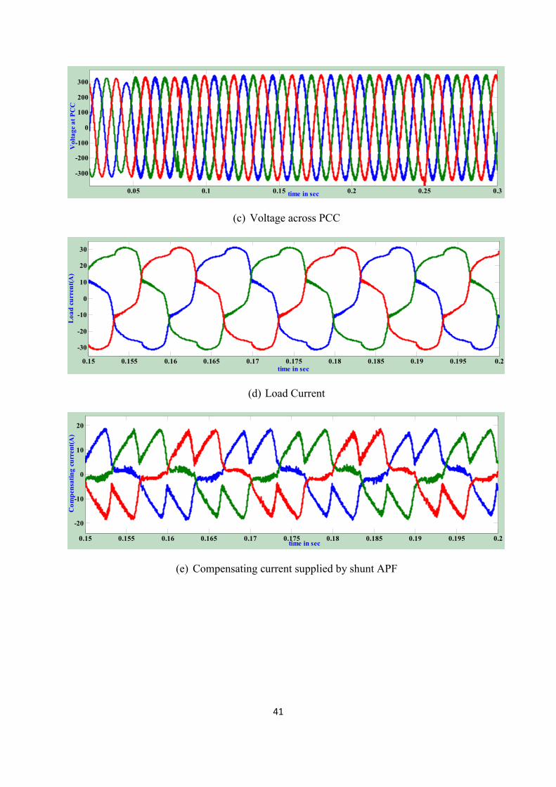
(c) Voltage across PCC
0.15 0.155 0.16 0.165 0.17 0.175 0.18 0.185 0.19 0.195 0.2
-30
-20
-10
0
10
20
30
time in sec
Lo
ad
cu
rren
t(A
)
(d) Load Current
0.15 0.155 0.16 0.165 0.17 0.175 0.18 0.185 0.19 0.195 0.2
-20
-10
0
10
20
time in sec
Co
mp
ensa
tin
g c
urr
ent(
A)
(e) Compensating current supplied by shunt APF
42
0.2 0.205 0.21 0.215 0.22 0.225 0.23 0.235 0.24 0.245 0.25
-30
-20
-10
0
10
20
30
time in sec
Sou
rce
curr
ent
in a
mp
s
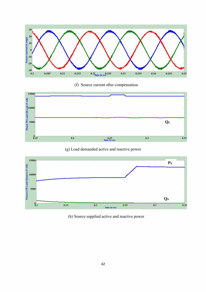
(f) Source current after compensation
0.15 0.2 0.25 0.3 0.350
5000
10000
15000
time in sec
Plo
ad
(W
) a
nd
QL
oa
d (
VA
R)
(g) Load demanded active and reactive power
0.1 0.15 0.2 0.25 0.3 0.350
5000
10000
15000
time in sec
Pso
urc
e (W
) a
nd
Qso
urc
e (V
AR
)
(h) Source supplied active and reactive power
QS
PS
QL
43
0.1 0.15 0.2 0.25 0.3 0.35
1000
2000
3000
4000
5000
time in sec
Pse
ries
(W
) a
nd
Qse
ries
(V
AR
)
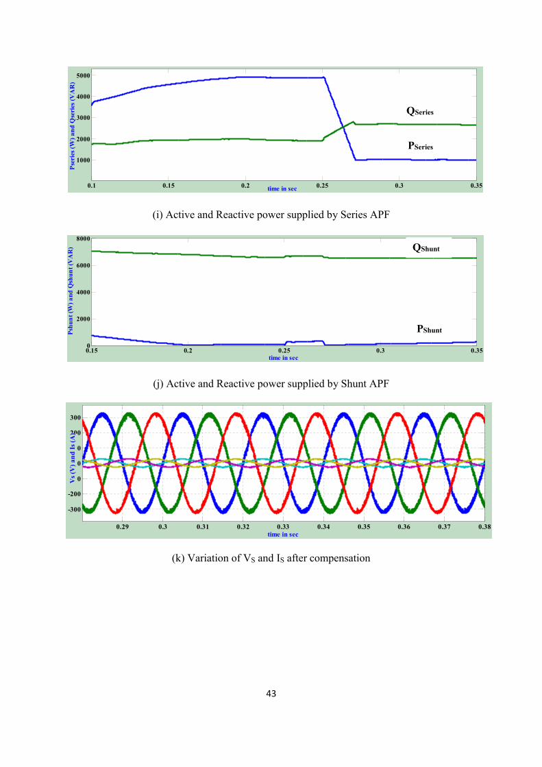
(i) Active and Reactive power supplied by Series APF
0.15 0.2 0.25 0.3 0.350
2000
4000
6000
8000
time in sec
Psh
un
t (W
) a
nd
Qsh
un
t (V
AR
)
(j) Active and Reactive power supplied by Shunt APF
0.29 0.3 0.31 0.32 0.33 0.34 0.35 0.36 0.37 0.38
-300
-200
-100
0
100
200
300
time in sec
Vs
(V)
an
d I
s (A
)
(k) Variation of VS and IS after compensation
QShunt
PShunt
PSeries
QSeries
44
0.15 0.155 0.16 0.165 0.17 0.175
-300
-200
-100
0
100
200
300
time in sec
VL
an
d V
s
power angle
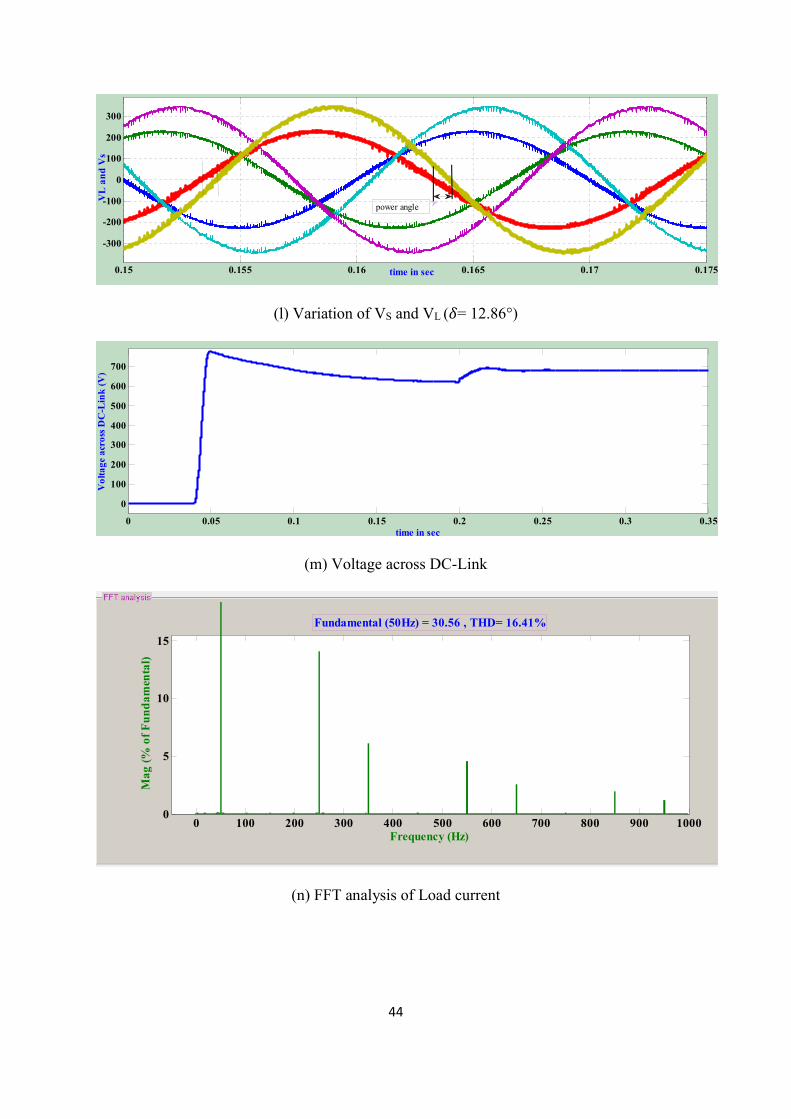
(l) Variation of VS and VL (�= 12.86°)
0 0.05 0.1 0.15 0.2 0.25 0.3 0.35
0
100
200
300
400
500
600
700
time in sec
Vo
lta
ge
acr
oss
DC
-Lin
k (
V)
(m) Voltage across DC-Link
0 100 200 300 400 500 600 700 800 900 10000
5
10
15
Frequency (Hz)
Fundamental (50Hz) = 30.56 , THD= 16.41%
Ma
g (
% o
f F
un
da
men
tal)
(n) FFT analysis of Load current
45
0 100 200 300 400 500 600 700 800 900 10000
5
10
15
20
25
Frequency (Hz)
Fundamental (50Hz) = 27.16 , THD= 0.70%
Ma
g (
% o
f F
un
da
men
tal)
(o) FFT analysis of Source current
Fig. 5.1 Simulation results under voltage sag condition
5.2 RESULTS FOR VOLTAGE SWELL
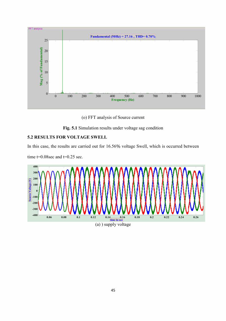
In this case, the results are carried out for 16.56% voltage Swell, which is occurred between
time t=0.08sec and t=0.25 sec.
0.06 0.08 0.1 0.12 0.14 0.16 0.18 0.2 0.22 0.24 0.26-400
-300
-200
-100
0
100
200
300
400
time in sec
So
urc
e V
olt
ag
e (V
)
(a) ) supply voltage
46
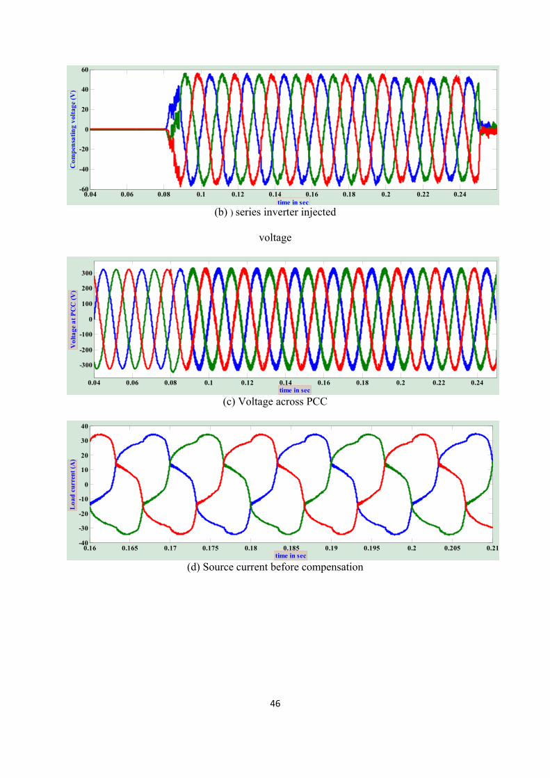
0.04 0.06 0.08 0.1 0.12 0.14 0.16 0.18 0.2 0.22 0.24-60
-40
-20
0
20
40
60
time in sec
Co
mp
ensa
tin
g v
olta
ge
(V)
(b) ) series inverter injected
voltage
0.04 0.06 0.08 0.1 0.12 0.14 0.16 0.18 0.2 0.22 0.24
-300
-200
-100
0
100
200
300
time in sec
Vo
lta
ge
at
PC
C (
V)
(c) Voltage across PCC
0.16 0.165 0.17 0.175 0.18 0.185 0.19 0.195 0.2 0.205 0.21-40
-30
-20
-10
0
10
20
30
40
time in sec
Lo
ad
cu
rren
t (A
)
(d) Source current before compensation
47
0.16 0.165 0.17 0.175 0.18 0.185 0.19 0.195 0.2 0.205 0.21
-20
-10
0
10
20
time in sec
Co
mp
ensa
tin
g c
urr
ent
(A)
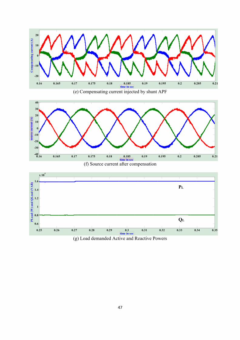
(e) Compensating current injected by shunt APF
0.16 0.165 0.17 0.175 0.18 0.185 0.19 0.195 0.2 0.205 0.21-40
-30
-20
-10
0
10
20
30
40
time in sec
sou
rce
curr
ent
(A)
(f) Source current after compensation
0.25 0.26 0.27 0.28 0.29 0.3 0.31 0.32 0.33 0.34 0.35
0.6
0.8
1
1.2
1.4
1.6
x 104
time in sec
PL
oa
d (
W)
an
d Q
Lo
ad
(V
AR
)
(g) Load demanded Active and Reactive Powers
QL
PL
48
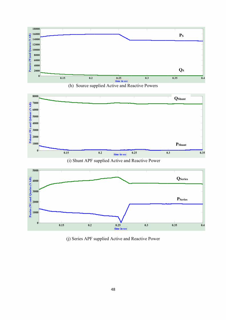
0.15 0.2 0.25 0.3 0.35 0.40
2000
4000
6000
8000
10000
12000
14000
16000
18000
time in sec
Pso
urc
e (W
)an
d Q
sou
rce
(VA
R)
(h) Source supplied Active and Reactive Powers
0.15 0.2 0.25 0.3 0.350
1000
2000
3000
4000
5000
6000
7000
8000
time in sec
Psh
un
t (W
) a
nd
Qsh
un
t (V
AR
)
(i) Shunt APF supplied Active and Reactive Power
0.15 0.2 0.25 0.3 0.35 0.40
1000
2000
3000
4000
5000
time in sec
Pse
ries
(W
) a
nd
Qse
ries
(V
AR
)
(j) Series APF supplied Active and Reactive Power
QShunt
PShunt
PSeries
QSeries
QS
PS
49
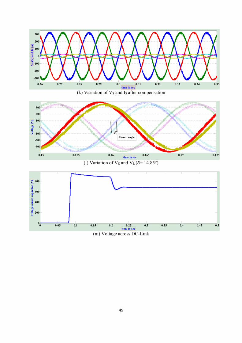
0.26 0.27 0.28 0.29 0.3 0.31 0.32 0.33 0.34 0.35
-300
-200
-100
0
100
200
300
time in sec
Vs
(V)
an
d I
s (A
)
(k) Variation of VS and IS after compensation
0.15 0.155 0.16 0.165 0.17 0.175
-300
-200
-100
0
100
200
300
time in sec
Vo
lta
ge
(V)
Power angle
(l) Variation of VS and VL (�= 14.85°)
0 0.05 0.1 0.15 0.2 0.25 0.3 0.35 0.4 0.45 0.50
200
400
600
800
time in sec
vo
ltag
e a
cro
ss c
apa
cito
r (V
)
(m) Voltage across DC-Link
50
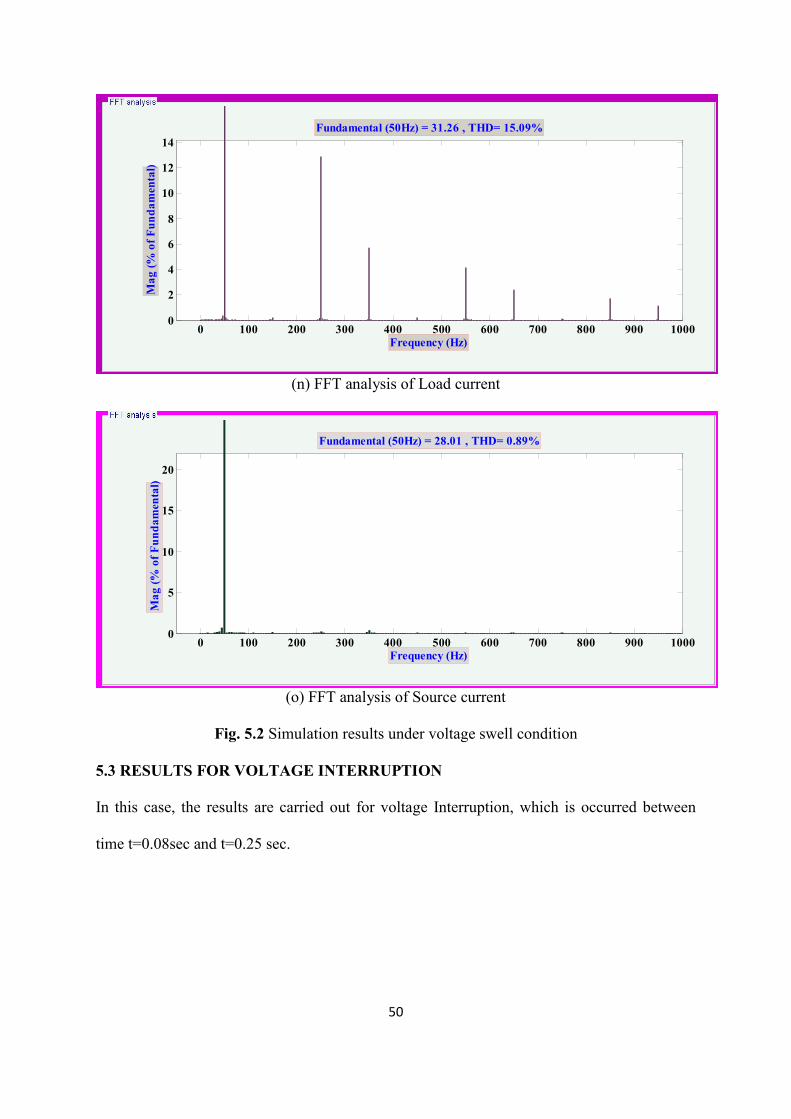
0 100 200 300 400 500 600 700 800 900 10000
2
4
6
8
10
12
14
Frequency (Hz)
Fundamental (50Hz) = 31.26 , THD= 15.09%
Ma
g (
% o
f F
un
da
men
tal)
(n) FFT analysis of Load current
0 100 200 300 400 500 600 700 800 900 10000
5
10
15
20
Frequency (Hz)
Fundamental (50Hz) = 28.01 , THD= 0.89%
Ma
g (
% o
f F
un
da
men
tal)
(o) FFT analysis of Source current
Fig. 5.2 Simulation results under voltage swell condition
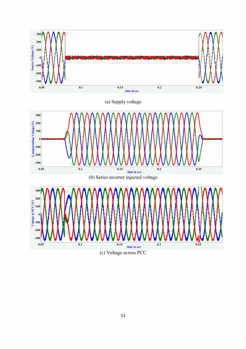
5.3 RESULTS FOR VOLTAGE INTERRUPTION
In this case, the results are carried out for voltage Interruption, which is occurred between
time t=0.08sec and t=0.25 sec.
51
0.05 0.1 0.15 0.2 0.25
-300
-200
-100
0
100
200
300
time in sec
So
urc
e V
olt
age
(V)
(a) Supply voltage
0.05 0.1 0.15 0.2 0.25
-300
-200
-100
0
100
200
300
time in sec
Com
pen
sati
ng
Vo
ltag
e (V
)
(b) Series inverter injected voltage
0.05 0.1 0.15 0.2 0.25
-300
-200
-100
0
100
200
300
time in sec
Vo
ltag
e at
PC
C (
V)
(c) Voltage across PCC
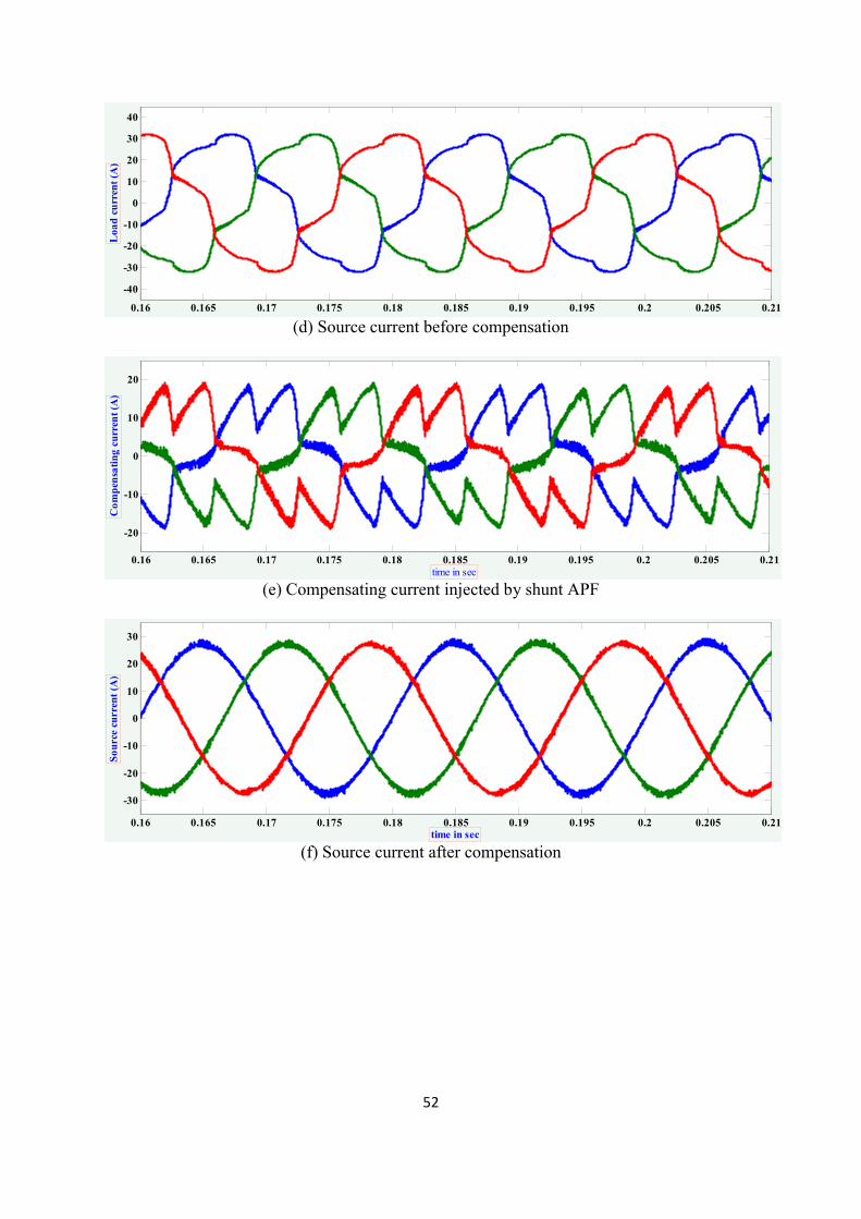
52
0.16 0.165 0.17 0.175 0.18 0.185 0.19 0.195 0.2 0.205 0.21
-40
-30
-20
-10
0
10
20
30
40L
oa
d c
urr
ent
(A)
(d) Source current before compensation
0.16 0.165 0.17 0.175 0.18 0.185 0.19 0.195 0.2 0.205 0.21
-20
-10
0
10
20
time in sec
Co
mp
ensa
tin
g c
urr
ent
(A)
(e) Compensating current injected by shunt APF
0.16 0.165 0.17 0.175 0.18 0.185 0.19 0.195 0.2 0.205 0.21
-30
-20
-10
0
10
20
30
time in sec
So
urc
e cu
rren
t (A
)
(f) Source current after compensation
53
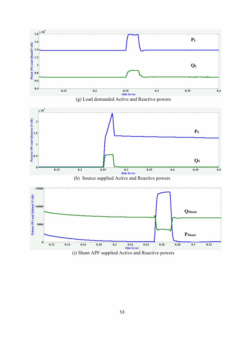
0.15 0.2 0.25 0.3 0.35 0.40.4
0.6
0.8
1
1.2
1.4
1.6
1.8x 10
4
time in sec
Plo
ad
(W
) a
nd
Qlo
ad
(VA
R)
(g) Load demanded Active and Reactive powers
0.15 0.2 0.25 0.3 0.35 0.4 0.45 0.50
0.5
1
1.5
2
x 104
time in sec
Pso
urc
e (W
) a
nd
Qso
urc
e (V
AR
)
(h) Source supplied Active and Reactive powers
0.12 0.14 0.16 0.18 0.2 0.22 0.24 0.26 0.28 0.3 0.320
5000
10000
15000
time in sec
Psh
un
t (W
) a
nd
Qsh
un
t (V
AR
)
(i) Shunt APF supplied Active and Reactive powers
PL
QL
PS
QS
PShunt
QShunt
54
0.1 0.15 0.2 0.25 0.30
0.5
1
1.5
2x 10
4
time in sec
Per
ies
(W)
an
d Q
seri
es (
VA
R)
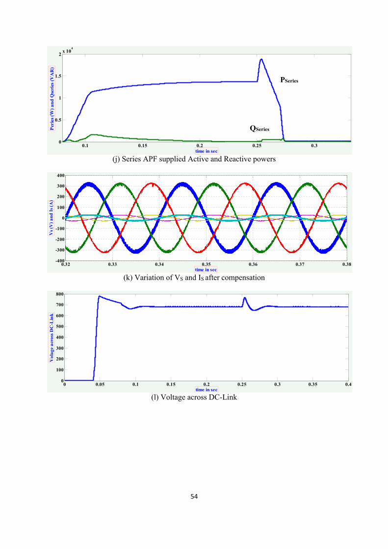
(j) Series APF supplied Active and Reactive powers
0.32 0.33 0.34 0.35 0.36 0.37 0.38-400
-300
-200
-100
0
100
200
300
400
time in sec
Vs
(V)
an
d I
s (A
)
(k) Variation of VS and IS after compensation
0 0.05 0.1 0.15 0.2 0.25 0.3 0.35 0.40
100
200
300
400
500
600
700
800
time in sec
Vo
lag
e a
cro
ss D
C-L
ink
(l) Voltage across DC-Link
PSeries
QSeries
55
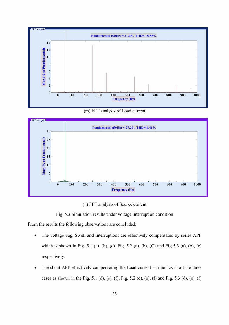
0 100 200 300 400 500 600 700 800 900 10000
2
4
6
8
10
12
14
Frequency (Hz)
Fundamental (50Hz) = 31.46 , THD= 15.53%
Ma
g (
% o
f F
un
da
men
tal)
(m) FFT analysis of Load current
0 100 200 300 400 500 600 700 800 900 10000
5
10
15
20
25
30
Frequency (Hz)
Fundamental (50Hz) = 27.29 , THD= 1.41%
Ma
g (
% o
f F
un
da
men
tal)
(n) FFT analysis of Source current
Fig. 5.3 Simulation results under voltage interruption condition
From the results the following observations are concluded:
The voltage Sag, Swell and Interruptions are effectively compensated by series APF
which is shown in Fig. 5.1 (a), (b), (c), Fig. 5.2 (a), (b), (C) and Fig 5.3 (a), (b), (c)
respectively.
The shunt APF effectively compensating the Load current Harmonics in all the three
cases as shown in the Fig. 5.1 (d), (e), (f), Fig. 5.2 (d), (e), (f) and Fig. 5.3 (d), (e), (f)
56
respectively. The THDs obtained are reduced to 0.7%, 0.89% and 1.41% from
16.41%, 15.09% and 15.53% respectively. The reason behind of obtaining such low
THD is the usage of HSF, which extracted the fundamental component thoroughly.
From the waveforms we can observe that the rms value of Load current is greater than
the rms value of source current and the values of Load currents are 23.72A, 23.08A
and 24.22A and of source current are 19.78A, 20.41A and 19.62A respectively.
As shown in fig. 5.1 (l) and fig. 5.2 (l) the power angle (�), between the source
voltage and load voltage is maintained at 12.86° and 14.85°.
As shown in the fig. 5.1 (j), 5.2 (j) and 5.3 (j) the Series inverter supplies both active
power and reactive power in all the three cases, which means, the injected voltage is
neither in series nor in quadrature with is. As it is supplying the reactive power
demanded by load at steady state, the burden on the shunt APF is reduced.
The advantage of Photo Voltaic System is observed from fig. 5.3 (h), (j) and (l), in the
Voltage interruption mode, which is switched at t=0.08sec. When it is on, the high
step-up DC-DC converter is maintaining nearly a constant voltage of 650 volts across
DC-Link from the position of rapidly drooping as shown in fig. 5.3 (l). During this
period, the entire load demanded power is supplied by series APF only i.e., source
supplied power is almost zero due to interruption. During the voltage sag and swell it
is switched at t=0.2 sec, and then on the voltage across DC-Link is maintained
constant as shown in fig. 5.1 (m) and fig. 5.2 (m) respectively.
The Load demanded power supply from Source, Shunt APF and Series APF are
shown in the above fig. 5.1 (g), (h), (i) and (j), fig. 5.2 (g), (h), (i), (j) and fig. 5.3 (g),
(h), (i) and (j) respectively. From these we can observe that, at steady state the active
power supplied by the shunt inverter is zero, i.e., it involves only in reactive power
compensation in steady state.
57
The operating source power factor is achieved to nearly unity in all the three cases as
shown in fig. 5.1 (k), fig. 5.2 (k) and fig. 5.3(k).
5.4 SUMMARY
This chapter demonstrates the effective compensation capabilities of the proposed
PV-UPQC system with the MATLB/SIMULINK results for the voltage sag, swell and
interruption cases. From the results it has shown that the PV-UPQC capable of supplying
long term power quality problems which avoids the individual back-up systems for the
end users. Using the power angle control scheme the burden and rating of the shunt APF,
which reduces the overall cost of the system. Apart from that here it also showed the
power flow analysis and improvement in power factor of the system.
The next chapter explains about the significant conclusions that are obtained using
proposed system.
58
CHAPTER 6
CONCLUSION
6.1 CONCLUSION
In this work the PV-UPQC is simulated for Voltage Sag, Swell and Interruption
modes using MATLAB SIMULINK and showed that the burden and on shunt APF is
reduced, which also reduces the overall rating and cost of UPQC. The PV-UPQC is showed
to be advantageous in order to supply power under voltage interruption mode and long
duration power quality issues, which cannot be done by the conventional UPQC and thus
improving the overall service reliability too. The usage of two high selectivity filters reduced
THD below acceptable level. The simulation results had shown the effectiveness of
mitigating voltage and current related problems. Overall the proposed PV-UPQC helps the
end users to avoid installation of individual back-up systems.
59
BIBLIOGRAPHY
[1] Vinod Khadkikar,“Enhancing electric power quality using UPQC:A comprehensive
overview,” IEEE Trans.Power Electron., vol. 27, no. 5, may 2012.
[2] V. Khadkikar and A. Chandra, “A new control philosophy for a unified power quality
conditioner (UPQC) to coordinate load-reactive power demand between shunt and series
inverters,” IEEE Trans. Power Del., vol. 23, no. 4, pp. 2522–2534, Oct. 2008.
[3] V. Khadkikar, A. Chandra, A. Barry, and T. Nguyen, “Analysis of powerflow in UPQC
during voltage sag and swell conditions for selection of device ratings,” in Proc. Can. Conf.
Electr. Comput. Eng., May 2006, pp. 867–872.
[4] Arindam Ghosh and Gerad Ledwich, Power Quality Enhancement Using CustomPower
Devices. NEW DELHI: Springer Publications, 2009.
[5] V. Khadkikar and A. Chandra, “UPQC-S: A novel concept of simultaneous voltage
sag/swell and load reactive power compensations utilizing series inverter of UPQC,” IEEE
Trans. Power Electron., vol. 26, no. 9, pp. 2414–2425, Sep. 2011.
[6] M. Basu, S. P. Das, and G. K. Dubey, “Investigation on the performance of UPQC-Q for
voltage sag mitigation and power quality improvement at a critical load point,” IET
Generation, Transmiss. Distrib., vol. 2, no. 3, pp. 414–423, May 2008.
[7] Mahesh K. Mishra and K. Karthikeyan, “Design and analysis of voltage source inverter
for active compensators to compensate unbalanced and non-linear loads”, International
Power Engineering Conference, IPEC 2007, pp. 649 –654.
[8] Y. Pal, A. Swarup, and B. Singh, “A comparative analysis of three-phase four-wire UPQC
topologies,” in Proc. Int. Conf. Power Electron. Drives Energy Syst., Dec. 20–23, 2010, pp.
1–6.
60
[9] F. Ng, M. C. Wong, and Y. D. Han, “Analysis and control of UPQC and its DC-link
power by use of p-q-r instantaneous power theory,” in Proc. Power Electron. Syst. Appl.,
Nov. 9–11, 2004, pp. 43–53.
[10] J. Tlusty and V. Valouch, “Effectiveness of unified power quality conditioner for flicker
mitigation,” in Proc. 4th Int. Power Electron. Motion Control Conf., Aug. 14–16, 2004, pp.
902–907.
[11] D. Kisck, V. Navrapescu, and M. Kisck,“Single-phase unified power quality conditioner
with optimum voltage angle injection for minimum VA requirement,” in Proc. IEEE Int.
Symp. Ind. Electron., Jun. 17–21, 2007, pp. 2443–2448.
[12] Y. Chen, X. Zha, J. Wang, H. Liu, J. Sun, and H. Tang, “Unified power quality
conditioner (UPQC): The theory, modeling and application,” in Proc. Int. Conf. Power Syst.
Technol., 2000, pp. 1329–1333.
[13] Suresh, M. Patnaik S.S. Suresh, Y., Panda A.K., "Comparison of two compensation
control strategies for shunt active power filter in three-phase four-wire system," Innovative
Smart Grid Technologies (ISGT), 2011 IEEE PES , vol., no., pp.1,6, 17-19 Jan. 2011.
[14] Akagi H, Kanazawa Y, and Nabae A, “Instantaneous reactive power compensators
comprising switching devices without energy storage components”, IEEE Trans. on Ind.l
Appl., Vol. IA-20, no. 3, pp. 625–630, 1984.
[15] Benhabib M.C., and Saadate S 2005, “New control approach for four-wire active
power filter based on the use of synchronous reference frame,” Elect.Power Syst. Res., Vol.
73 (2005) 353–362.
[16] Abdusalam M., Poure P., Karimi S., and Saadate S, “New digital reference current
generation for shunt active power filter under distorted voltage conditions”, Elect.Power Syst.
Res., Vol. 79, pp. 759–765, 2009.
61
[17] Esram T. and Chapman P. L., “Comparison of photovoltaic array maximum power point
tracking techniques,” IEEE Trans. Energy Conv.,vol. 22, no. 2, pp. 439–449, 2007.
[18] “Photovoltaic power conditioning system with line connection,” IEEE Trans. Ind.
Electron., vol. 53, no. 4, august 2006.
[19] B. Singh, K. Al-Haddad, and A. Chandra, “A review of active filters for power quality
improvement,” IEEE Trans. Ind. Electron., vol. 46, no. 5, pp. 960–971, Oct. 1999.
[20] Karimi, S., Poure, P., Saadate, S., "High performances reference current generation for
shunt active filter under distorted and unbalanced conditions, "Power Electronics Specialists
Conference, PESC 2008. IEEE, vol., no., pp.195, 201, 15-19 June 2008.
[21] Mesbahi, N.; Ouari, A.; Omeiri, A., "Reference current computation for three-level shunt
active filter under distorted and unbalanced conditions," Renewable and Sustainable Energy
Conference (IRSEC), 2013 International , vol., no., pp.343,347, 7-9 March 2013.
[22] Karimi, S., Poure, P., Saadate, S., "Reference current generation without PLL for shunt
active filter under distorted and unbalanced conditions," IEEE International Symposium on
Industrial Electronics, 2008 , vol., no., pp.363,368, June 30 2008-July 2 2008.
[23] Abdusalam, M.; Poure, P.; Saadate, S., "Study and experimental validation of harmonic
isolation based on High Selectivity Filter for three-phase active filter," IEEE International
Symposium on Industrial Electronics, 2008., vol., no., pp.166,171, June 30 2008-July 2 2008.
[24] Hsieh Y P, Chen J F, Liang T J and Yang L S 2011, “Novel high set-up DC–DC
converter for distributed generation system”, IEEE Trans. Ind Electron., vol.60,no.4,pp.1473-
1482.
[25] Femia, N., Petrone, G., Spagnuolo, G., Vitelli M., "Optimization of perturb and observe
maximum power point tracking method," Power Electronics, IEEE Transactions on , vol.20,
no.4, pp.963,973, July 2005.