Embed Size (px)
Citation preview
AFSC5G26D37
1RF Device DataNXP Semiconductors
Power Amplifier Module for LTE and5GThe AFSC5G26D37 is a fully integrated Doherty power amplifier module
des igned for wire less infras t ructure appl icat ions that demand highperformance in the smallest footprint. Ideal for applications in massive MIMOsystems, outdoor small cells, and low power remote radio heads. Thefield--proven LDMOS power amplifiers are designed for TDD and FDD LTEsystems.
Typical LTE Performance: Pout = 5 W Avg., VDD = 28 Vdc, 1 20 MHz LTE,Input Signal PAR = 8 dB @ 0.01% Probability on CCDF. (1)
Carrier CenterFrequency
Gain(dB)
ACPR(dBc)
PAE(%)
2575 MHz 27.4 –27.8 40.0
2600 MHz 27.2 –27.9 39.9
2625 MHz 27.1 –27.7 40.0
1. All data measured with device soldered in NXP reference circuit.
Features
Frequency: Designed for 2545–2655 MHz. Operates across 2496–2690 MHz. Advanced high performance in--package Doherty Fully matched (50 ohm input/output, DC blocked) Designed for low complexity analog or digital linearization systems
Document Number: AFSC5G26D37Rev. 4, 05/2019
NXP SemiconductorsTechnical Data
2496–2690 MHz, 27 dB, 5 W Avg.AIRFAST POWER AMPLIFIER
MODULE
AFSC5G26D37
10 mm 6 mm Module
2017–2019 NXP B.V.
2RF Device Data
NXP Semiconductors
AFSC5G26D37
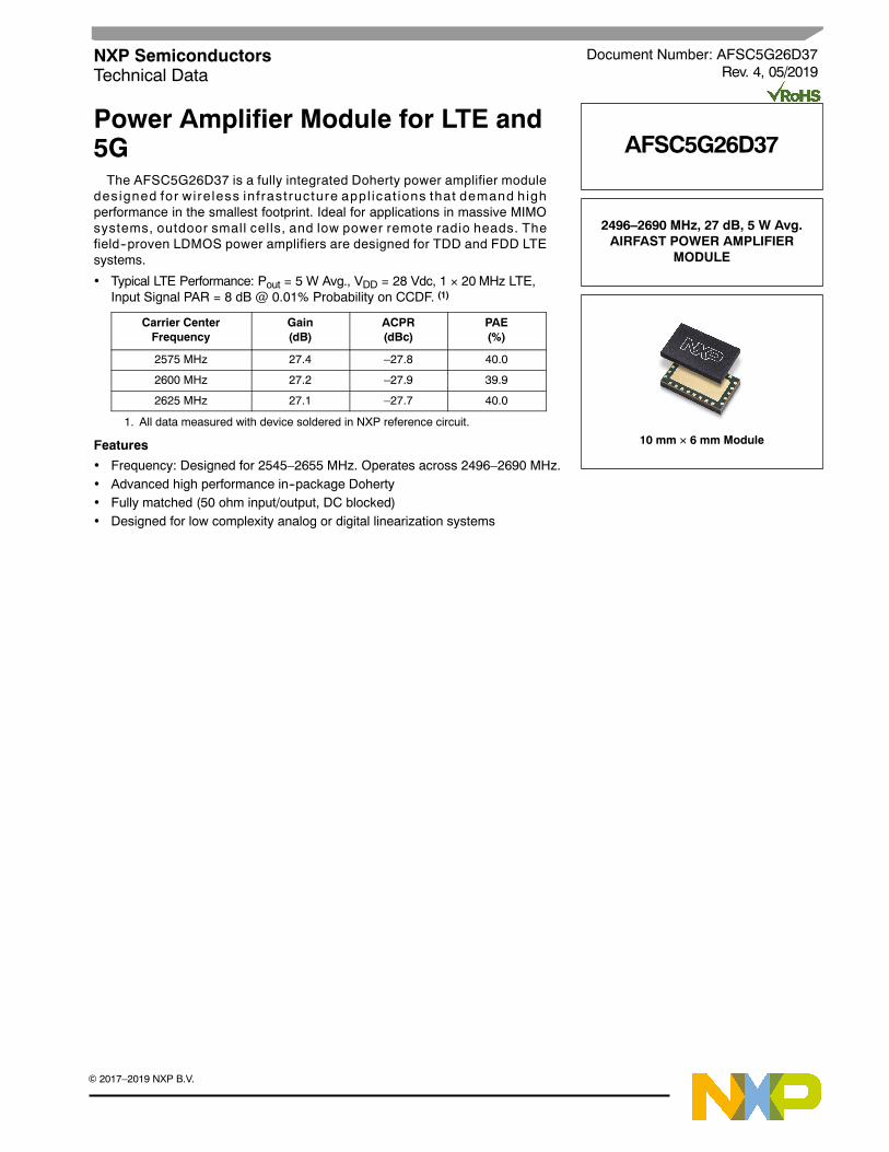
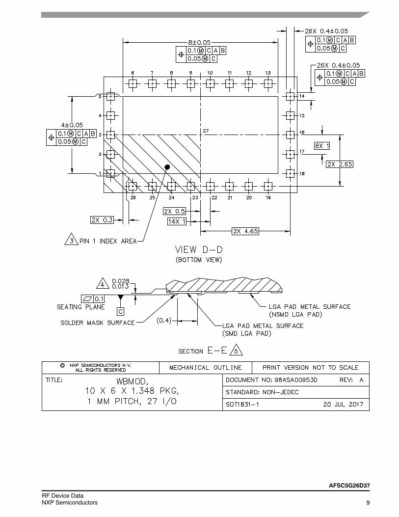
(Bottom View)
19 20 21 22 23 24 25 26
13 12 11 10 9 8 7 6
16
14
15
17
18
5
4
3
2
1
27
Pin 1index area
Figure 1. Pin Connections
Note: Exposed backside of the package is DC and RF ground.
(Top View)
GND
GND
GND
GND
GND
GND
GND
GND
26 25 24 23 22 21 20 19
VGP2
VGP1
VGC1
VGC2
VDC1
VDC2
GND
6 7 8 9 10 11 12 13
RFin
VDP1
VDP2
GND
5
4
3
2
1
GND
GND
GND
RFout
GND
14
15
16
17
18
Pin 1index area
GND
GND
AFSC5G26D37
3RF Device DataNXP Semiconductors
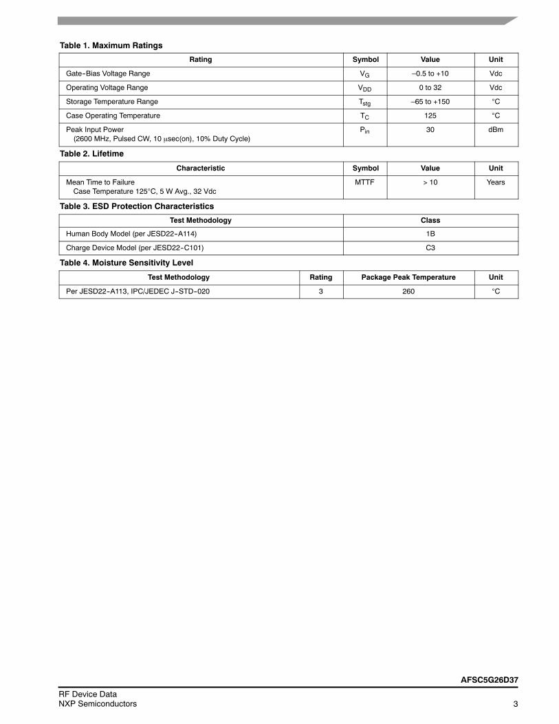
Table 1. Maximum Ratings
Rating Symbol Value Unit
Gate--Bias Voltage Range VG –0.5 to +10 Vdc
Operating Voltage Range VDD 0 to 32 Vdc
Storage Temperature Range Tstg –65 to +150 C
Case Operating Temperature TC 125 C
Peak Input Power(2600 MHz, Pulsed CW, 10 sec(on), 10% Duty Cycle)
Pin 30 dBm
Table 2. Lifetime
Characteristic Symbol Value Unit
Mean Time to FailureCase Temperature 125C, 5 W Avg., 32 Vdc
MTTF > 10 Years
Table 3. ESD Protection Characteristics
Test Methodology Class
Human Body Model (per JESD22--A114) 1B
Charge Device Model (per JESD22--C101) C3
Table 4. Moisture Sensitivity Level
Test Methodology Rating Package Peak Temperature Unit
Per JESD22--A113, IPC/JEDEC J--STD--020 3 260 C
4RF Device Data
NXP Semiconductors
AFSC5G26D37
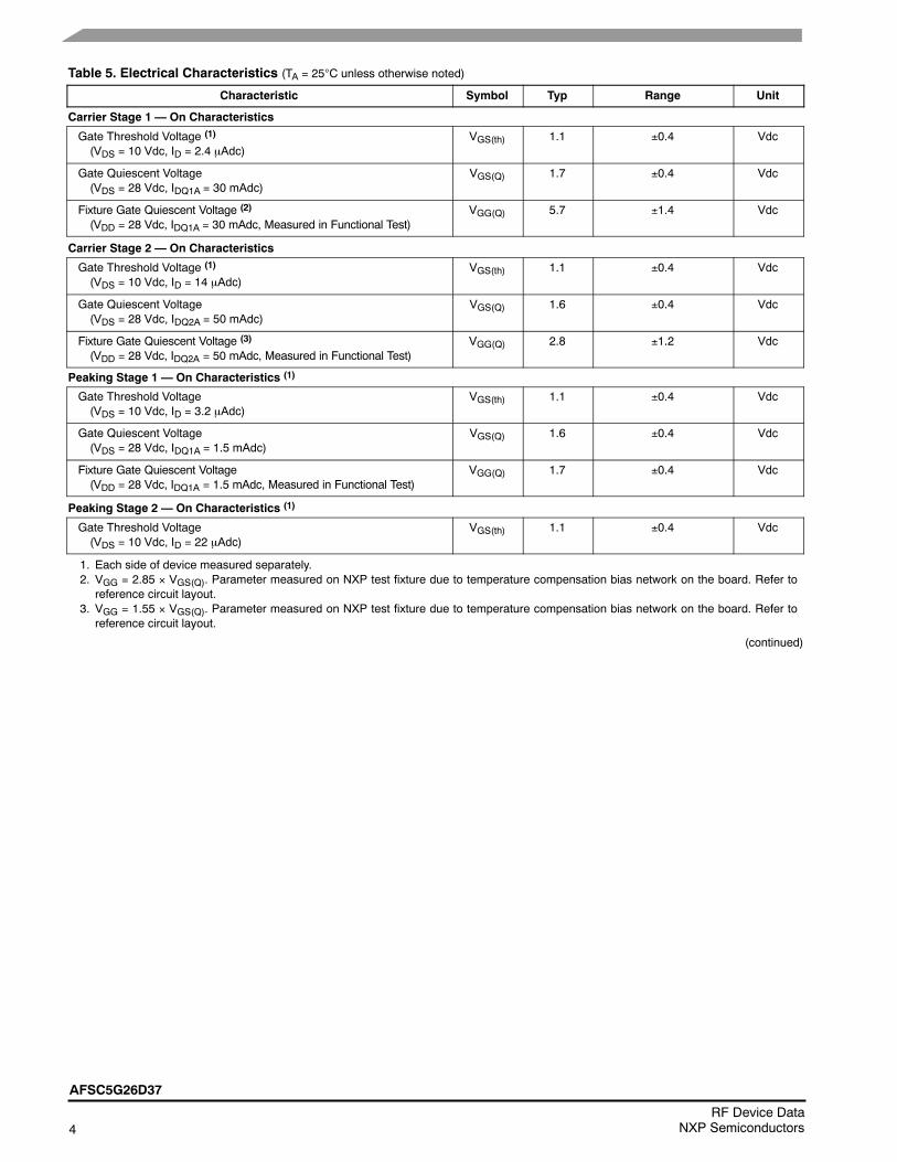
Table 5. Electrical Characteristics (TA = 25C unless otherwise noted)
Characteristic Symbol Typ Range Unit
Carrier Stage 1 — On Characteristics
Gate Threshold Voltage (1)
(VDS = 10 Vdc, ID = 2.4 Adc)VGS(th) 1.1 0.4 Vdc
Gate Quiescent Voltage(VDS = 28 Vdc, IDQ1A = 30 mAdc)
VGS(Q) 1.7 0.4 Vdc
Fixture Gate Quiescent Voltage (2)
(VDD = 28 Vdc, IDQ1A = 30 mAdc, Measured in Functional Test)VGG(Q) 5.7 1.4 Vdc
Carrier Stage 2 — On Characteristics
Gate Threshold Voltage (1)
(VDS = 10 Vdc, ID = 14 Adc)VGS(th) 1.1 0.4 Vdc
Gate Quiescent Voltage(VDS = 28 Vdc, IDQ2A = 50 mAdc)
VGS(Q) 1.6 0.4 Vdc
Fixture Gate Quiescent Voltage (3)
(VDD = 28 Vdc, IDQ2A = 50 mAdc, Measured in Functional Test)VGG(Q) 2.8 1.2 Vdc
Peaking Stage 1 — On Characteristics (1)
Gate Threshold Voltage(VDS = 10 Vdc, ID = 3.2 Adc)
VGS(th) 1.1 0.4 Vdc
Gate Quiescent Voltage(VDS = 28 Vdc, IDQ1A = 1.5 mAdc)
VGS(Q) 1.6 0.4 Vdc
Fixture Gate Quiescent Voltage(VDD = 28 Vdc, IDQ1A = 1.5 mAdc, Measured in Functional Test)
VGG(Q) 1.7 0.4 Vdc
Peaking Stage 2 — On Characteristics (1)
Gate Threshold Voltage(VDS = 10 Vdc, ID = 22 Adc)
VGS(th) 1.1 0.4 Vdc
1. Each side of device measured separately.2. VGG = 2.85 VGS(Q). Parameter measured on NXP test fixture due to temperature compensation bias network on the board. Refer to
reference circuit layout.3. VGG = 1.55 VGS(Q). Parameter measured on NXP test fixture due to temperature compensation bias network on the board. Refer to
reference circuit layout.
(continued)
AFSC5G26D37
5RF Device DataNXP Semiconductors
Table 5. Electrical Characteristics (TA = 25C unless otherwise noted) (continued)
Characteristic Symbol Min Typ Max Unit
Functional Tests (1) (In NXP Doherty Production ATE (2) Test Fixture, 50 ohm system) VDD = 28 Vdc, IDQ1A = 30 mA, IDQ2A = 50 mA,VGS1B = (Vt – 0.105) (3) Vdc, VGS2B = (Vt – 0.321) (3) Vdc, Pout = 5 W Avg., Two--tone CW, f1 = 2575 MHz, f2 = 2635 MHz, 60 MHz ToneSpacing.
Gain G 23.3 24.9 28.3 dB
Drain Efficiency D 31.0 35.1 — %
Intermodulation Distortion IM3 — –25.3 –20.0 dBc
Pout @ 3 dB Compression Point f1 = 2498.5 MHzf2 = 2687.5 MHz
P3dB 42.542.3
44.643.2
——
dBm
Wideband Ruggedness (4) (In NXP Doherty Power Amplifier Module Reference Circuit, 50 ohm system) IDQ1A = 30 mA, IDQ2A = 50 mA,VGSP1 = 1.5 Vdc, VGSP2 = 1.3 Vdc, f = 2600 MHz, Additive White Gaussian Noise (AWGN) with 10 dB PAR
ISBW of 400 MHz at 28 Vdc, 13 W Avg. Modulated Output Power(6 dB Input Overdrive from 5 W Avg. Modulated Output Power)
No Device Degradation
Typical Performance (4) (In NXP Doherty Power Amplifier Module Reference Circuit, 50 ohm system) VDD = 28 Vdc, IDQ1A = 30 mA,IDQ2A = 50 mA, VGSP1 = 1.5 Vdc, VGSP2 = 1.3 Vdc, Pout = 5 W Avg., 2600 MHz Bandwidth
VBW Resonance Point, 2--tone, 1 MHz Tone Spacing(IMD Third Order Intermodulation Inflection Point)
VBWres — 150 — MHz
Quiescent Current Accuracy over Temperature (5)
with 2.2 k Gate Feed Resistors (–40 to 85C) Stage 1with 2.2 k Gate Feed Resistors (–40 to 85C) Stage 2
IQT——
1.02.0
——
%
1--carrier 20 MHz LTE, 8 dB Input Signal PAR
Gain G — 27.2 — dB
Power Added Efficiency PAE — 39.9 — %
Adjacent Channel Power Ratio ACPR — –27.9 — dBc
Adjacent Channel Power Ratio ALT1 — –34.6 — dBc
Adjacent Channel Power Ratio ALT2 — –41.0 — dBc
Output Peak--to--Average Ratio @ 0.01% Probability PAR — 8.0 — dB
Gain Flatness (6) GF — 0.3 — dB
Fast CW, 27 ms Sweep
Pout @ 3 dB Compression Point P3dB — 45.7 — dBm
AM/PM @ P3dB — –23 —
Pulsed CW, 10 sec(on), 10% Duty Cycle @ P1dB
Gain Variation over Temperature(–40C to +105C)
G — 0.033 — dB/C
Output Power Variation over Temperature(–40C to +105C)
P1dB — 0.018 — dB/C
Table 6. Ordering Information
Device Tape and Reel Information Package
AFSC5G26D37T2 T2 Suffix = 2,000 Units, 24 mm Tape Width, 13--inch Reel 10 mm 6 mm Module
1. Part input and output matched to 50 ohms.2. ATE is a socketed test environment.3. Refer to AN12071, Doherty Biasing Methodology for Volume Production. Go to http://www.nxp.com/RF and search for AN12071.4. All data measured in fixture with device soldered in NXP reference circuit.5. Refer to AN1977, Quiescent Current Thermal Tracking Circuit in the RF Integrated Circuit Family, and to AN1987, Quiescent Current
Control for the RF Integrated Circuit Device Family. Go to http://www.nxp.com/RF and search for AN1977 or AN1987.6. Gain flatness = Max(G(fLow to fHigh)) – Min(G(fLow to fHigh))
6RF Device Data
NXP Semiconductors
AFSC5G26D37
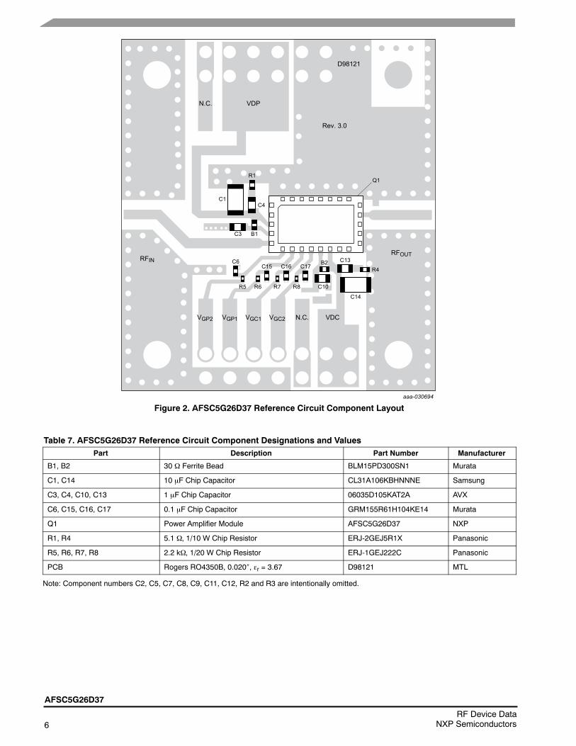
Figure 2. AFSC5G26D37 Reference Circuit Component Layout
N.C. VDP
RFIN
VGP2 VGP1 VGC1 VGC2
RFOUT
VDCN.C.
R1
B1C3
C6C15 C16 C17
B2 C13
R4
R5 R6 R7 R8 C10
C14
C1C4
D98121
Rev. 3.0
aaa-030694
Q1
Table 7. AFSC5G26D37 Reference Circuit Component Designations and ValuesPart Description Part Number Manufacturer
B1, B2 30 Ferrite Bead BLM15PD300SN1 Murata
C1, C14 10 F Chip Capacitor CL31A106KBHNNNE Samsung
C3, C4, C10, C13 1 F Chip Capacitor 06035D105KAT2A AVX
C6, C15, C16, C17 0.1 F Chip Capacitor GRM155R61H104KE14 Murata
Q1 Power Amplifier Module AFSC5G26D37 NXP
R1, R4 5.1 , 1/10 W Chip Resistor ERJ-2GEJ5R1X Panasonic
R5, R6, R7, R8 2.2 k, 1/20 W Chip Resistor ERJ-1GEJ222C Panasonic
PCB Rogers RO4350B, 0.020, r = 3.67 D98121 MTL
Note: Component numbers C2, C5, C7, C8, C9, C11, C12, R2 and R3 are intentionally omitted.
AFSC5G26D37
7RF Device DataNXP Semiconductors
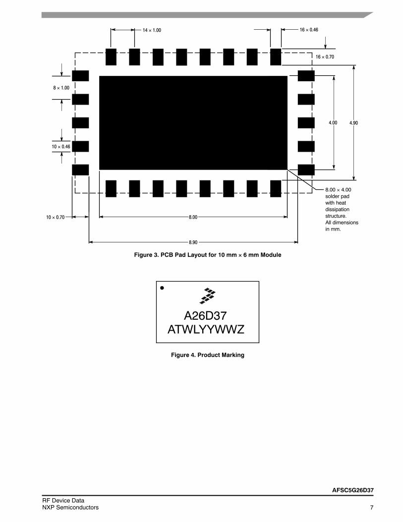
Figure 3. PCB Pad Layout for 10 mm 6 mm Module
8.00 4.00solder padwith heatdissipationstructure.All dimensionsin mm.
16 0.46
16 0.70
10 0.46
8 1.00
10 0.70
14 1.00
8.00
8.90
4.904.00
Figure 4. Product Marking
A26D37ATWLYYWWZ
8RF Device Data
NXP Semiconductors
AFSC5G26D37
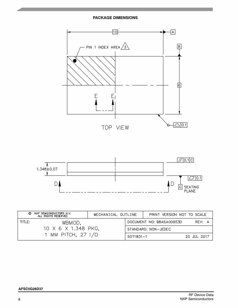
PACKAGE DIMENSIONS
AFSC5G26D37
9RF Device DataNXP Semiconductors
10RF Device Data
NXP Semiconductors
AFSC5G26D37
AFSC5G26D37
11RF Device DataNXP Semiconductors
PRODUCT DOCUMENTATION AND TOOLS
Refer to the following resources to aid your design process.
Application Notes AN1977: Quiescent Current Thermal Tracking Circuit in the RF Integrated Circuit Family
AN1987: Quiescent Current Control for the RF Integrated Circuit Device Family
AN12071: Doherty Biasing Methodology for Volume Production
Development Tools Printed Circuit Boards
FAILURE ANALYSIS
At this time, because of the physical characteristics of the part, failure analysis is limited to electrical signature analysis.In cases where NXP is contractually obligated to perform failure analysis (FA) services, full FA may be performed by thirdparty vendors with moderate success. For updates contact your local NXP Sales Office.
REVISION HISTORY
The following table summarizes revisions to this document.
Revision Date Description
0 Sept. 2017 Initial release of data sheet
1 Feb. 2018 DC tests, On Characteristics, Peaking Stage 1, VGS(Q), VGG(Q): corrected IDQ1A value to show correctdecimal placement and rounded 1.45 to 1.5 mAdc, p. 3
2 May 2018 Typical Performance table: table header updated to show data in table is typical LTE performance, p. 1
Table 5, Typical Performance section, Gain Flatness: updated to reflect actual test conditions used formeasurement; P3dB and AM/PM: updated test condition to “Fast CW, 27 ms Sweep” to reflect actual testcondition for measurement, p. 4
Table 6, Ordering Information: AFSC5G26D37T1 tape and reel option replaced with AFSC5G26D37T2 toreflect current production shipping format, p. 4
Fig. 2, Reference Circuit Component Layout: updated layout to the standard design which is compatible forall power amplifier module products, p. 5
Table 7, Reference Circuit Component Designations and Values: updated table to replace recentlydiscontinued components for C1, C14 (10 F chip capacitors) and C3, C4, C10, C13 (1 F chipcapacitors), p. 5
3 Dec. 2018 Typical LTE Performance table: changed “3 x 20 MHz LTE” to “1 x 20 MHz LTE” to reflect how data wasmeasured in the table, p. 1
4 May 2019 Added Wideband Ruggedness table, p. 5
General updates made to align data sheet to current standard
12RF Device Data
NXP Semiconductors
AFSC5G26D37
Document Number: AFSC5G26D37Rev. 4, 05/2019
Information in this document is provided solely to enable system and softwareimplementers to use NXP products. There are no express or implied copyright licensesgranted hereunder to design or fabricate any integrated circuits based on the informationin this document. NXP reserves the right to make changes without further notice to anyproducts herein.
NXP makes no warranty, representation, or guarantee regarding the suitability of itsproducts for any particular purpose, nor does NXP assume any liability arising out of theapplication or use of any product or circuit, and specifically disclaims any and all liability,including without limitation consequential or incidental damages. “Typical” parametersthat may be provided in NXP data sheets and/or specifications can and do vary indifferent applications, and actual performance may vary over time. All operatingparameters, including “typicals,” must be validated for each customer application bycustomer’s technical experts. NXP does not convey any license under its patent rightsnor the rights of others. NXP sells products pursuant to standard terms and conditions ofsale, which can be found at the following address: nxp.com/SalesTermsandConditions.
NXP, the NXP logo, Freescale, the Freescale logo and Airfast are trademarks ofNXP B.V. All other product or service names are the property of their respective owners.E 2017–2019 NXP B.V.
How to Reach Us:
Home Page:nxp.com
Web Support:nxp.com/support