Embed Size (px)
Citation preview

2
1
6
7
4 17 15 14
10 kW
18 13 12
8 10 16 20 19 9
0.01mF
PROG GND GND A0 A1 TIMER
VREF
EN
SDA
SCL
VS VINP VCC SENSE VINM GATE VOUT
2 mW
11PG
10 kW
10kW
190 kW
33 kW
0.01 mF
0.01 mF
9 V to 26 V
3.3 V to 5 V
TPS2480/1
TPS2480TPS2481
www.ti.com SLUS939B –APRIL 2010–REVISED DECEMBER 2010
Positive Voltage Intelligent Protection DeviceHotswap Controller and I2C Current Monitor
Check for Samples: TPS2480, TPS2481
1FEATURES DESCRIPTION• Programmable FET Power Limit The TPS2480/81 are designed to minimize inrush into
applications and protect both the load and the FET• External N-Channel FET Gate Drivefrom over-current or short circuit events. They control• Programmable Fault Timeran external N-channel MOSFET switch and provide
• Open Drain Power Good Output accurate voltage, current, and power monitoring using• I2C monitoring of Current, Voltage and Power a configurable 12 bit A/D converter via an I2C
interface. The independently adjustable power limit• High Accuracy Current Monitoringand current limit ensure that the external MOSFET(1% over temperature)operates within the FET's Safe Operating Area
• Dynamic Calibration (SOA).• 9-V to 26-V Input Range
The flexible design includes a Power Good outputwhich can be used for sequencing as well as load
APPLICATIONS fault indication. An external timer capacitor can set• Servers the fault time to help immunize the system from
nuisance shutdowns during brief transient events.• Hard Drives• Storage Networks The monitoring circuitry incorporates a high accuracy• Base Stations A/D converter which can be configured from a 9 to 13
bit converter. The internal gain of the A/D can beconfigured to scale the current, voltage and powerreadings to the needs of the application. An additionalmultiplying register calculates power in Watts. TheI2C interface uses multi-level addressing to allow upto 16 programmable addresses.
Simplified Application Diagram
1
Please be aware that an important notice concerning availability, standard warranty, and use in critical applications of TexasInstruments semiconductor products and disclaimers thereto appears at the end of this data sheet.
PRODUCTION DATA information is current as of publication date. Copyright © 2010, Texas Instruments IncorporatedProducts conform to specifications per the terms of the TexasInstruments standard warranty. Production processing does notnecessarily include testing of all parameters.

TPS2480TPS2481SLUS939B –APRIL 2010–REVISED DECEMBER 2010 www.ti.com
DESCRIPTION (CONT.)The TPS2480 and TPS2481 monitors shunts on buses that can vary from 9 V to 26 V and with a few externalcomponents it is possible to monitor buses as high as 80 V.
The monitoring circuitry uses a single 3-V to 5.5-V supply, drawing a maximum of 1 mA of supply current.
DEVICE INFORMATION (1)
JUNCTIONDEVICE PACKAGE FUNCTION MARKINGTEMPERATURE
TPS2480 -40°C to 125°C PW20 Latch Off TPS2480
TPS2481 -40°C to 125°C PW20 Auto Retry TPS2481
(1) For package and ordering information see the Package Option Addendum at the end of this document or see the TI Web site atwww.ti.com.
DISSIPATION RATINGS (1) (2) (3)
PACKAGE qJA HIGH K, °C/W qJA (Air Flow) HIGH-k (4), °C/W
TPS2480 88.3 74.5
TPS2481 88.3 74.5
(1) Tested per JEDEC JESD51, natural convection. The definitions of high-k and low-k are per JESD 51-7and JESD 51-3.(2) Low-k (2 signal - no plane, 3 in. by 3 in. board, 0.062 in. thick, 1 oz. copper) test board with the pad soldered, and an additional 0.12
in.2 of top-side copper added to the pad.(3) High-k is a (2 signal – 2 plane) test board with the pad soldered.(4) The best case thermal resistance is obtained using the recommendations per SLMA002A (2 signal - 2 plane with the pad connected to
the plane).
RECOMMENDED OPERATING CONDITIONSover operating free-air temperature range (unless otherwise noted)
MIN NOM MAX UNIT
VCC Input voltage range 9 80V
PROG Input voltage range 0.4 4
VREF Sourcing current 0 1 mA
VS Input voltage range 3 5.5V
VINP, VINM Input voltage range (1) 0 24
Tstg Operating free air temperature -40 85°C
TJ Operating junction temperature -40 125
(1) Hotswap circuits may experience voltage surges during events such as hotplug and output shorts. The maximum RecommendedOperating Voltage is derated below the Absolute Maximum to allow for tolerance of protection devices (clamps). If the application doesnot have input surges, the TPS2480 may be used up to its Absolute Maximum Rating with no degradation of performance or reliability.
2 Submit Documentation Feedback Copyright © 2010, Texas Instruments Incorporated
Product Folder Link(s): TPS2480 TPS2481

TPS2480TPS2481
www.ti.com SLUS939B –APRIL 2010–REVISED DECEMBER 2010
ABSOLUTE MAXIMUM RATINGS (1) (2) (3)
over operating free-air temperature range (unless otherwise noted)UNIT
Input voltage range, VCC, Sense, Enable, OUT -0.3 to 100
Supply voltage, VS GND - 0.3 to 6
Input voltage, common mode, VINP, VINM GND- 0.3 to + 26
Input voltage, differential, VINP, VINM -26 to + 26 V
Input voltage range, PROG -0.3 to 6
Output voltage range, GATE, PG -0.3 to 100
Output voltage range, TIMER, VREF -0.3 to 6
Sink current, PG 10
Source current, VREF 0 to 2 mA
Sink current, PROG 2
SDA GND- 0.3 to + 6.0V
SCL GND- 0.3 to VS + 0.3
Current into SDA, SCL, VS, VINP, VINM, A0, A1, GNDB 5mA
Open drain digital output current 10
ESD rating, HBM 2 kV
ESD rating, CDM 500
Operating junction temperature range, TJ - 40 to + 125°C
Storage temperature range, Tstg - 40 to 150
(1) Stresses beyond those listed under “absolute maximum ratings” may cause permanent damage to the device. These are stress ratingsonly, and functional operation of the device at these or any other conditions beyond those indicated under “recommended operatingconditions” is not implied. Exposure to absolute–maximum–rated conditions for extended periods may affect device reliability.
(2) All voltage values are with respect to GND unless otherwise stated.(3) Do not apply voltage to these pins.
Copyright © 2010, Texas Instruments Incorporated Submit Documentation Feedback 3
Product Folder Link(s): TPS2480 TPS2481

TPS2480TPS2481SLUS939B –APRIL 2010–REVISED DECEMBER 2010 www.ti.com
ELECTRICAL CHARACTERISTICSover operating free-air temperature range (unless otherwise noted)
PARAMETER TEST CONDITIONS MIN TYP MAX UNIT
Supply Current (VCC)
Enabled VEN = Hi VSENSE = VOUT = VVCC 450 1000IVCC mA
Disabled VEN = Lo VSENSE = VVCC = VOUT = 0 90 250
Quiescent current operating 0.7 1.0 mAIVS
Quiescent current Power down mode 6 15 mA
VPOR Power On reset threshold 2 V
Current Sense Input (SENSE)
ISENSE Input bias current VSENSE = VVCC VOUT = VVCC 7.5 20 mA
Reference Voltage Output (VREF)
VREF Reference voltage 0 < IVREF < 1 mA 3.9 4 4.1 V
Power Limiting Input (PROG)
Input bias current; deviceIPROG 0 < VPROG < 4 V VEN = 48 V 5 mAenabled; sourcing or sinking
Pulldown resistance; deviceRPROG IPROG = 200 mA; VEN = 0 V 375 600 Ωdisabled
Power Limiting and Current Limiting (SENSE)
Current sense threshold VPROG = 2.4 V; VOUT = 0 V or VPROG = 0.9 V; VOUTVCL V(VCC-SENSE) with power 17 25 33= 30 V; VVCC = 48 Vlimiting tripmV
Current sense thresholdVSENSE V(VCC-sense) without power VPROG = 4 V; VSENSE = VOUT 45 50 55
limiting trip
VPROG = 4 V; VOUT = VSENSE; V(VCC-SENSE): 0Large overload response timetF_TRIP rising to 200 mV; C(GATE-OUT) = 2 nF; V(GATE-OUT) = 1.2 msto GATE low 1 V
Timer Operation (TIMER)
VTIMER = 0 V 15.0 25.0 34.0ISOURCE Charge current (sourcing)
VTIMER = 0 V; TJ = 25°C 20.0 25.0 30.0mA
VTIMER = 5 V 1.50 2.5 3.70ISINK Discharge current (sinking)
VTIMER = 5 V; TJ = 25°C 2.10 2.5 3.10
TIMER upper threshold 3.9 4.0 4.1voltageV
TIMER lower reset threshold TPS2481 only 0.96 1.0 1.04voltage
DRETRY Fault retry duty cycle TPS2481 only 0.5% 0.75% 1.0%
Gate Drive Output (GATE)
IGATE GATE sourcing current VSENSE = VVCC; V(GATE-OUT) = 7 V; VEN = Hi 15 22 35 mA
VEN = Lo; VGATE = VVCC 1.8 2.4 2.8GATE sinking current mA
VEN = Hi; VGATE = VVCC; V(VCC-SENSE)³ 200 mV 75 125 250
VGATE-OUT GATE output voltage 12 16 V
Propagation delay: EN going VEN = 0 → 2.5 V, 50% of VEN to 50% of VGATE,tD_ON 25 40true to GATE output high VOUT = VVCC, R(GATE-OUT) = 1 MOhm
Propagation delay: EN going VEN = 2.5 V → 0 V, 50% of VEN to 50% of VGATE,tD_OFF false (0 V) to GATE output 0.5 1 msVOUT = VVCC, R(GATE-OUT) = 1 MΩ, tFALL < 0.1 mslow
Propagation delay: TIMER VTIMER: 0 → 5 V, tRISE < 0.1 ms. 50% of VTIMER to 0.8 1expires to GATE output low 50% of VGATE, VOUT = VCC , R(GATE-OUT) = 1 MΩ,
4 Submit Documentation Feedback Copyright © 2010, Texas Instruments Incorporated
Product Folder Link(s): TPS2480 TPS2481

TPS2480TPS2481
www.ti.com SLUS939B –APRIL 2010–REVISED DECEMBER 2010
ELECTRICAL CHARACTERISTICS (continued)over operating free-air temperature range (unless otherwise noted)
PARAMETER TEST CONDITIONS MIN TYP MAX UNIT
Power Good Output (PG)
IPG = 2 mA 0.1 0.25VPG_L Low voltage (sinking)
IPG = 4 mA 0.25 0.5
PG threshold voltage; VOUTVPGTL VSENSE = VVCC; measure V(VCC-OUT) 0.8 1.25 1.7rising; PG goes open drain VPG threshold voltage; VOUTVPGTH VSENSE = VVCC; measure V(VCC-OUT) 2.2 2.7 3.2falling; PG goes low
PG threshold hysteresisVHYST_PG VSENSE = VVCC 1.4voltage; V(SENSE-OUT)
PG deglitch delay; detectiontDPG to output; rising and falling VSENSE = VVCC 5 9 15 ms
edges
Leakage current; PG false; open drain 10 mA
Output Voltage Feedback Input (OUT)
VOUT = VVCC, VEN = Hi; sinking 8 20IOUT Bias current mA
VOUT = GND; VEN = Lo; sourcing 18 40
Enable Input (EN)
VEN_H Threshold VEN going high 1.32 1.35 1.38V
VEN_L Threshold VEN going low 1.20 1.25 1.30
VEN hysteresis 100 mV
Leakage current VEN = 30 V 1 mA
Input Supply UVLO (VCC)
VVCC turn on Rising 8.4 8.8V
VVCC turn off Falling 7.2 8.3
Hysteresis 75 mV
Digital Inputs (SDA in input mode, SCL, A0, A1 )
CIN Input capacitance 3 pF
ILEAKAGE Input leakage current 0 < VIN < VS 0.1 1 mA
VIN HI Logic Hi input level 0.7(VS) 6
VINLO Logic low input level -0.3 0.3(VS) V
VHYS Hysteresis 0.5
Open Drain Digital Output (SDA)
VLO SDA Low Output Sinking 5 mA 0.15 0.4 V
ILEAKAGE High level leakage current VOUT = VS 0.1 1.0 mA
Copyright © 2010, Texas Instruments Incorporated Submit Documentation Feedback 5
Product Folder Link(s): TPS2480 TPS2481

TPS2480TPS2481SLUS939B –APRIL 2010–REVISED DECEMBER 2010 www.ti.com
ELECTRICAL CHARACTERISTICS (continued)over operating free-air temperature range (unless otherwise noted)
PARAMETER TEST CONDITIONS MIN TYP MAX UNIT
Input
PGA = x 1 0 ±40
PGA = x 2 0 ±80Full-scale current sense mV(input) voltage range PGA = x 4 0 ±160
PGA = x 8 0 ±320
BRNG = 1 0 32Bus voltage (input voltage) Vrange BRNG = 0 0 16
Common-mode rejection VIN+ = 0 V to 26 V 100 120 dBCMRR
PGA = x 1 ±10 ±100
PGA = x 2 ±20 ±125Input offset mV
PGA = x 4 ±30 ±150VOS
PGA = x 8 ±40 ±200
Temp stability 0.1 mV/°C
PSRR VS = 3 V to 5.5 V 10 mV/V
CSA gain error ±0.04%GainCSA
Temp stability 10 ppm
IVNP 20 mAInput bias current Active mode
IVINM 20 || 320 mA || kΩILEAKAGE IVNP, IVINM Power down mode, leakage input current 0.1 ±0.5 mA
A/D Converter
Shunt voltage 10 mVStep Size 1 LSB
Bus voltage 4 mV
Current Current measurement Error ±0.2% ±0.5%Accuracy
Temp drift Over full range ±1.0%
Voltage Bus voltage measurement Error ±0.2% ±0.5%Accuracy
Temp drift ( -25°C to 85°C ) Over full range ±1.0%
12 Bit 532 586
11 Bit 276 304TCONV Conversion time
10 Bit 148 163 ms
9 Bit 84 92
TLOWCONV Conversion time Minimum A/D conversion time 4
6 Submit Documentation Feedback Copyright © 2010, Texas Instruments Incorporated
Product Folder Link(s): TPS2480 TPS2481

15
8
6
10
9
7
13
12
11
1
2
20
19
+
+
Enable
UVLOEnable
POR
EN
GND
1.35V/
1.25V
8.4V/
8.3V
14SENSE
S
S
+2.7V/
1.25V
PROG
VCC
Enable
Inrush complete
9-ms
Deglitch
TIMER
PG
OUT
Fault
Logic
+
25m A
2.5m A
4V/1V
+
14V
GATE
2mA
Charge
Pump 22m A
Gate Control
Amplifier
4V
ReferenceVREF
Constant
Power
Engine
Voltage Register
Current Register
Power RegisterX
I2C
Interface
4
16
18
17
PGA ADC
A1
A0
SCL
SDA
VSVINM
VINP
GND
A
B
A2B
50mV maxV(DS) Detector
I(D) Detector
For autoretry option
with duty cycle of 75%
TPS2480TPS2481
www.ti.com SLUS939B –APRIL 2010–REVISED DECEMBER 2010
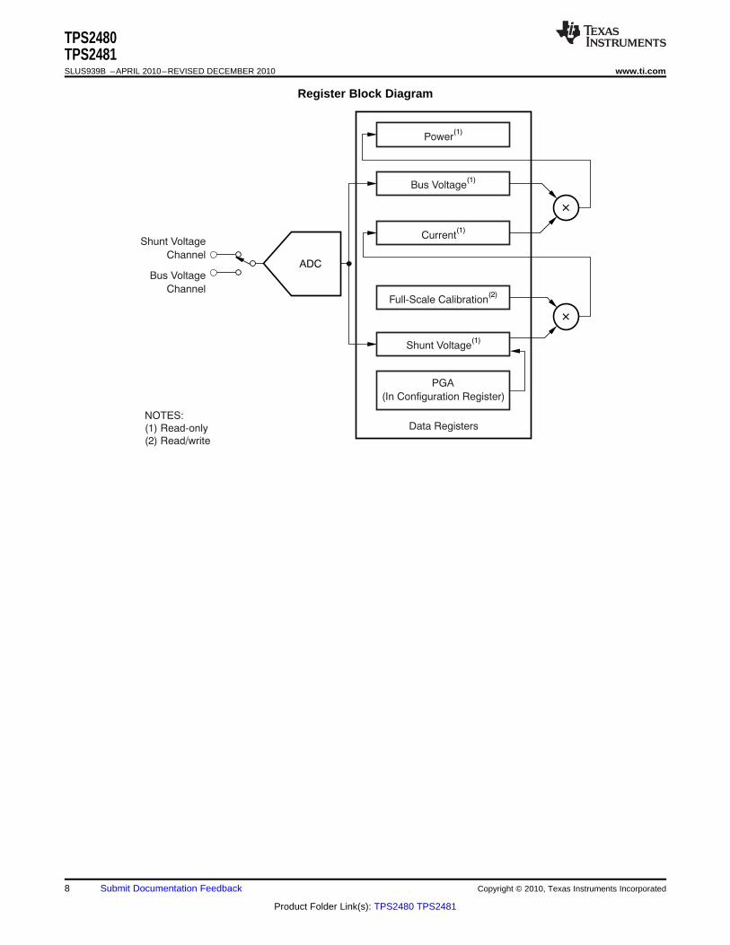
DEVICE INFORMATION
Functional Block Diagram
Copyright © 2010, Texas Instruments Incorporated Submit Documentation Feedback 7
Product Folder Link(s): TPS2480 TPS2481
ADC
´
´
Shunt Voltage
Channel
Bus Voltage
Channel
PGA
(In Configuration Register)
Shunt Voltage(1)
Data Registers
Full-Scale Calibration(2)
Current(1)
Bus Voltage(1)
Power(1)
NOTES:
(1) Read-only
(2) Read/write
TPS2480TPS2481SLUS939B –APRIL 2010–REVISED DECEMBER 2010 www.ti.com
Register Block Diagram
8 Submit Documentation Feedback Copyright © 2010, Texas Instruments Incorporated
Product Folder Link(s): TPS2480 TPS2481

1
2
3
4
5
6
7
8
9
10
SDA
SDL
NC
VS
NC
EN
VREF
PROG
TIMER
GND
20
19
18
17
16
15
14
13
12
11
A0
A1
VINM
VINP
GND
VCC
SENSE
GATE
OUT
PG
TPS2480/81
TPS2480TPS2481
www.ti.com SLUS939B –APRIL 2010–REVISED DECEMBER 2010
20-Pin TSSOP
Table 1. TERMINAL FUNCTIONS
FUNCTION TPS2480/81 DESCRIPTION
SDA 1 I2C Data Line
SCL 2 I2C Clock
NC 3 Tie to GND or float
VS 4 Power input to the I2C block, 3.3 V to 5 V
NC 5 No connection, tie to GND or float
EN 6 Device enable
VREF 7 Reference voltage output, used to set power threshold on PROG pin
PROG 8 Power-limit setting input
TIMER 9 Fault timing capacitor
GND 10 GND
PG 11 Power good reporting output, open-drain
OUT 12 Output voltage feedback
GATE 13 Gate output
SENSE 14 Current-limit sense input
VCC 15 Main power supply input to device and FET
GND 16 GND
VINP 17 Positive differential shunt voltage. Connect to positive side of shunt resistor
Negative differential shunt voltage. Connect to negative side of shunt resistor. Bus voltage isVINM 18 measured from this pin to GND
A1 19 Address pin. Table 2 shows pin settings and corresponding addresses.
A0 20 Address pin. Table 2 shows pin settings and corresponding addresses.
Copyright © 2010, Texas Instruments Incorporated Submit Documentation Feedback 9
Product Folder Link(s): TPS2480 TPS2481

( )LIM
PROG
LIM
PV
10 I=
´
J(max) S(max)
LIM
JC(max)
T TP
Rq
-<
TPS2480TPS2481SLUS939B –APRIL 2010–REVISED DECEMBER 2010 www.ti.com
Pin Description
A0, A1: Address pins for setting the TPS2480 I2C address. These bits can be tied to one of four pins ( GND,SDA, SCL, VS ) which gives a total of 16 different address as shown in Table 2.
EN: The GATE driver is enabled if the positive threshold is exceeded and the internal POR and UVLO thresholdshave been satisfied. EN can be used as a logic control input, an analog input voltage monitor as illustrated byR1/R2 in the Functional Block Diagram, or it can be tied to VCC to always enable the TPS2480/81. Thehysteresis associated with the internal comparator makes this a stable method of detecting a low input conditionand shutting the downstream circuits off. A TPS2480 that has latched off can be reset by cycling EN below itsnegative threshold and back high.
GATE: Provides the high side (above VCC) gate drive for the external FET. It is controlled by the internal gatedrive amplifier, which provides a pull-up of 22 mA from an internal charge pump and a strong pull-down to groundof 75 mA (min). The pull-down current is a non-linear function of the amplifier overdrive; it provides small drive forsmall overloads, but large overdrive for fast reaction to an output short. There is a separate pull-down of 2 mA toshut the external FET off when EN or UVLO causes this to happen. An internal clamp protects the gate of theexternal FET (to OUT) and generally eliminates the need for an external clamp in almost all cases for deviceswith 20-V VGS(max) ratings; an external Zener may be required to protect the gate of devices with VGS(max) < 16 V.A small series resistance of 10 Ω should be inserted in the gate lead if the CISS of the external FET > 200 pF,otherwise use 33 Ω for small MOSFETs. A capacitor can be connected from GATE to ground to create a slowerinrush with a constant current profile without affecting the amplifier stability. Add a series resistor of about 1 kΩ tothe gate capacitor to maintain the gate clamping and current limit response time.
GND: This pin is connected to system ground.
OUT: This input pin is used by the constant power engine and the PG comparator to measure VDS of the externalFET as V(SENSE-OUT). Internal protection circuits leak a small current from this pin when it is low. If the load circuitcan drive OUT below ground, connect a clamp (or freewheel) diode from OUT (cathode) to GND (anode).
PG: This open-drain output is intended to interface to downstream dc/dc converters or monitoring circuits. PGgoes open-drain (high voltage with a pull-up) after VDS of the external FET has fallen to about 1.25 V and a 9-msdeglitch time period has elapsed. PG is false (low or low resistance to ground) whenever EN is false, VDS of theexternal FET is above 2.7 V, or UVLO is active. PG can also be viewed as having an input and output voltagemonitor function. The 9-ms deglitch circuit operates to filter short events that could cause PG to go inactive (low)such as a momentary overload or input voltage step. VPG voltage can be greater than VVCC because its ESDprotection is only with respect to ground.
PROG: The voltage applied to this pin (0.4 V to 4.0 V) programs the power limit used by the constant powerengine. Normally, a resistor divider R3/R4 is connected from VREF to PROG to set the power limit according tothe following equation:
(1)
where PLIM is the desired power limit of the external FET and ILIM is the current limit setpoint (see SENSE). PLIMis determined by the desired thermal stress on the external FET:
(2)
where TJ(max) is the maximum desired transient junction temperature of the external FET and TS(max) is themaximum case temperature prior to a start or restart.
VPROG is used in conjunction with VDS to compute the (scaled) current, ID_ALLOWED, by the constant power engine.ID_ALLOWED is compared by the gate amplifier to the actual ID, and used to generate a gate drive. If ID <ID_ALLOWED, the amplifier turns the gate of the external FET full on because there is no overload condition;otherwise GATE is regulated to maintain the ID = ID_ALLOWED relationship. A capacitor may be tied from PROG to
10 Submit Documentation Feedback Copyright © 2010, Texas Instruments Incorporated
Product Folder Link(s): TPS2480 TPS2481

LIM
S
50mVI
R=
6
F TT C 1347 10= ´ ´
TPS2480TPS2481
www.ti.com SLUS939B –APRIL 2010–REVISED DECEMBER 2010
ground to alter the natural constant power inrush current shape. If properly designed, the effect is to cause theleading step of current in Figure 12 to look like a ramp. PROG is internally pulled to ground whenever EN, POR,or UVLO are not satisfied or the TPS2480 is latched off. This feature serves to discharge any capacitanceconnected to the pin. Do not apply voltages greater than 4 V to PROG. If the constant power limit is not used,PROG should be tied to VREF through a 47-kΩ resistor.
SCL: This pin is the clock input for the I2C interface.
SDA: This pin is the data input for the I2C interface.
SENSE: Monitors the voltage at the drain of the external FET, and the downstream side of RS providing theconstant power limit engine with feedback of both the external FET current (ID) and voltage (VDS). Voltage isdetermined by the difference between SENSE and OUT, while the current analog is the difference between VCCand SENSE. The constant power engine uses VDS to compute the allowed ID and is clamped to 50 mV, actinglike a traditional current limit at low VDS. The maximum current limit is set by the following equation:
(3)
Design the connections to SENSE to minimize RS voltage sensing errors. Don't drive SENSE to a large voltagedifference from VCC because it is internally clamped to VCC. The current limit function can be disabled byconnecting SENSE to VCC.
TIMER: An integrating capacitor, CT, connected to the TIMER pin provides a timing function that controls thefault-time for both versions and the restart interval for the TPS2481. The timer charges at 25 mA whenever theTPS2480/81 is in power limit or current limit and discharges at 2.5 mA otherwise. The charge-to-discharge currentratio is constant with temperature even though there is a positive temperature coefficient to both. If TIMERreaches 4 V, the TPS2480 pulls GATE to ground, latches off, and discharges CT. The TPS2491 pulls GATE toground and attempt a restart (re-enable GATE) after a timing sequence consisting of discharging CT down to 1 Vfollowed by 15 more charge and discharge cycles. The TPS2480 can be reset by either cycling the EN pin or theUVLO (e.g. power cycling). TIMER discharges when EN is low or UVLO or POR are active. The TIMER pinshould be tied to ground if this feature is not used. The general equation for fault retry time as a function of CT is:
(4)
VCC: This pin is associated with three functions:1. biasing power to the integrated circuit,2. input to power on reset (POR) and under voltage lockout (UVLO) functions, and3. voltage sense at one terminal of RS for the external FET current measurement.
The voltage must exceed the POR (about 6 V for roughly 400 ms) and the internal UVLO (about 8 V) beforenormal operation (driving the GATE) may begin. Connections to VCC should be designed to minimize RS voltagesensing errors and to maximize the effect of C1 and D1; place C1 at RS rather than at the device pin to eliminatetransient sensing errors. GATE, PROG, PG, and TIMER are held low when either UVLO or POR are active.
VINM: This pin is Kelvin connected to the negative (load) side of the current sensing resistor. It will appear toexternal circuitry as a 20-mA sink in parallel with a 320-kΩ resistor to GND.
VINP: This pin is Kelvin connected to the positive (source) side of the current sensing resistor. It will typically sink~ 20 mA.
VS: Power source for the logic and I2C interface. Typically between 3 V and 5 V.
VREF: Provides a 4.0-V reference voltage for use in conjunction with the resistor divider of a typical applicationcircuit to set the voltage on the PROG pin. The reference voltage is available once the internal POR and UVLOthresholds have been met. It is not designed as a supply voltage for other circuitry, therefore ensure that no morethan 1 mA is drawn. Although not typically required, up to 1000 pF can be placed on this pin.
Copyright © 2010, Texas Instruments Incorporated Submit Documentation Feedback 11
Product Folder Link(s): TPS2480 TPS2481

2.0
1.5
1.0
0.5
0
-0.5
-1.0
-1.5
0 5 10 15 20 25
Inp
ut
Cu
rre
nts
(m
A)
V Voltage (V)IN-
30
VS+ = 5V
V 5VS+ =
VS+ = 3V
V 3VS+ =
100
80
60
40
20
0
-20
-40
-60
-80
-100-40 -25 0 25 50 75 100
Off
se
t (
V)
m
Temperature ( C)°
125
160mV Range
320mV Range
80mV Range 40mV Range
100
80
60
40
20
0
-20
-40
-60
-80
-100-40 -25 0 25 50 75 100
Ga
in E
rro
r (m
%)
Temperature ( C)°
125
320mV Range 160mV Range
80mV Range 40mV Range
50
45
40
35
30
25
20
15
10
5
0-40 -25 0 25 50 75 100
Off
se
t (m
V)
Temperature ( C)°
125
32V Range 16V Range
-40 -25 0 25 50 75 100 125
100
80
60
40
20
0
-20
-40
-60
-80
-100
Ga
in E
rro
r (m
%)
Temperature ( C)°
32V
16V
20
15
10
5
0
-5
-10
-15
-20-0.4 -0.3 -0.2 -0.1 0 0.1 0.2 0.3
INL
(V
)m
Input Voltage (V)
0.4
TPS2480TPS2481SLUS939B –APRIL 2010–REVISED DECEMBER 2010 www.ti.com
TYPICAL CHARACTERISTICSA/D FREQUENCY RESPONSE ADC SHUNT OFFSET vs TEMPERATURE
Figure 1. Figure 2.
ADC SHUNT GAIN ERROR vs TEMPERATURE ADC BUS VOLTAGE OFFSET vs TEMPERATURE
Figure 3. Figure 4.
ADC BUS GAIN ERROR vs TEMPERATURE INTEGRAL NONLINEARITY vs INPUT VOLTAGE
Figure 5. Figure 6.
12 Submit Documentation Feedback Copyright © 2010, Texas Instruments Incorporated
Product Folder Link(s): TPS2480 TPS2481

0
-10
-20
-30
-40
-50
-60
-70
-80
-90
-10010 100 1k 10k 100k 1M
Ga
in (
dB
)
Input Frequency (Hz)
1.2
1.0
0.8
0.6
0.4
0.2
0
-40 -25 0 25 50 75 100
I(m
A)
Q
Temperature ( C)°
125
V = 3VS
V = 5VS
16
14
12
10
8
6
4
2
0-40 -25 0 25 125
I(
A)
mQ
Temperature ( C)°
V = 5VS
V = 3VS
50 75 100
1.0
0.9
0.8
0.7
0.6
0.5
0.4
0.3
0.2
0.1
0
1k 10k 100k 1M 10M
I Q(m
A)
SCL Frequency (Hz)
V = 5VS
V =S 3V
300
250
200
150
100
50
0
1k 10k 100k 1M 10M
I(
A)
Qm
SCL Frequency (Hz)
V = 5VS
V = 3VS
TPS2480TPS2481
www.ti.com SLUS939B –APRIL 2010–REVISED DECEMBER 2010
TYPICAL CHARACTERISTICS (continued)INPUT CURRENTS WITH LARGE DIFFERENTIAL
VOLTAGES(VIN+ at 12V, Sweep of VIN–) ACTIVE IQ vs TEMPERATURE
Figure 7. Figure 8.
SHUTDOWN IQ vs TEMPERATURE ACTIVE IQ vs I2C CLOCK FREQUENCY
Figure 9. Figure 10.
SHUTDOWN IQ vs I2C CLOCK FREQUENCY
Figure 11.
Copyright © 2010, Texas Instruments Incorporated Submit Documentation Feedback 13
Product Folder Link(s): TPS2480 TPS2481

TPS2480TPS2481SLUS939B –APRIL 2010–REVISED DECEMBER 2010 www.ti.com
APPLICATION INFORMATION
Basic Operation
The TPS2480/81 provides all the features needed for a positive hotswap controller.
These features include:1. Under-voltage lockout;2. Adjustable (system-level) enable;3. Turn-on inrush limit;4. High-side gate drive for an external N-channel MOSFET;5. MOSFET protection (power limit and current limit);6. Adjustable overload timeout (also called an electronic circuit breaker);7. Charge-complete indicator for downstream converter sequencing; and8. Optional automatic restart mode.
The TPS2480/81 features superior power-limiting, MOSFET protection that allows independent control of currentlimit (to set maximum full-load current), power limit and overload time (to keep FET in its SOA), and overloadtime (to control case temperature rise). The typical application circuit, and oscilloscope plots of Figure 12 andFigure 16 demonstrate many of the functions described above.
Board Plug-In (Figure 12)
Only the bypass capacitor charge current and small bias currents are evident when a board is first plugged in.The TPS2480/81 is held inactive, and GATE, PROG, TIMER, and PG are held low for less than 1 ms whileinternal voltages stabilize, then GATE, PROG, TIMER, and PG are released and the part begins sourcing currentto the GATE pin and the external FET begins to turn on while the voltage across it, V(SENSE-OUT), and currentthrough it, V(VCC-SENSE), are monitored. Current initially rises to the value which satisfies the power limit engine(PLIM÷VVCC) since the output capacitor was discharged.
14 Submit Documentation Feedback Copyright © 2010, Texas Instruments Incorporated
Product Folder Link(s): TPS2480 TPS2481

TPS2480TPS2481
www.ti.com SLUS939B –APRIL 2010–REVISED DECEMBER 2010
TIMER and PG Operation (Figure 12)
The TIMER pin charges CT as long as limiting action continues, and discharges at a 1/10 charge rate whenlimiting stops. If the voltage on CT reaches 4 V before the output is charged, the external FET is turned off andeither a latch-off or restart cycle commences, depending on the part type. The open-drain PG output provides adeglitched end-of-charge indication which is based on the voltage across the external FET. PG is useful forpreventing a downstream DC-to-DC converter from starting while CO is still charging. PG goes active (opendrain) about 9 ms after CO is charged. This delay allows the external FET to fully turn on and any transients inthe power circuits to end before the converter starts up. The resistor pull-up shown on pin PG in the typicalapplication diagram only demonstrates operation; the actual connection to the converter depends on theapplication. Timing can appear to terminate early in some designs if operation transitions out of the power limitmode into a gate charge limited mode at low VDS values.
Figure 12. Basic Board Insertion
Copyright © 2010, Texas Instruments Incorporated Submit Documentation Feedback 15
Product Folder Link(s): TPS2480 TPS2481

TPS2480TPS2481SLUS939B –APRIL 2010–REVISED DECEMBER 2010 www.ti.com
Action of the Constant Power Engine (Figure 13)
The calculated power dissipated in the external FET, VDS x ID, is computed under the same startup conditions asFigure 12. The current of the external FET, labeled IIN, initially rises to the value that satisfies the constant powerengine; in this case it is 54 W / 48 V = 1.1 A. The 54-W value is programmed into the engine by setting thePROG voltage using Equation 1. VDS of the external FET, which is calculated as V(SENSE-OUT) , falls as COcharges, thus allowing the the external FET drain current to increase. This is the result of the internal constantpower engine adjusting the current limit reference to the GATE amplifier as CO charges and VDS falls. Thecalculated device power in Figure 13, labeled MOSFET POWER, is seen to be flat-topped and constant withinthe limitations of circuit tolerance and acquisition noise. A fixed current limit is implemented by clamping theconstant power engine output to 50 mV when VDS is low. This protection technique can be viewed as aspecialized form of foldback limiting; the benefit over linear foldback is that it yields the maximum output currentfrom a device over the full range of VDS and still protects the device.
Figure 13. Computation of the External FET Stress During Startup
16 Submit Documentation Feedback Copyright © 2010, Texas Instruments Incorporated
Product Folder Link(s): TPS2480 TPS2481

TPS2480TPS2481
www.ti.com SLUS939B –APRIL 2010–REVISED DECEMBER 2010
Response to a Hard Output Short (Figure 14 and Figure 15)
Figure 14 shows the short circuit response over the full time-out period. This begins when the output voltage fallsand ends when the external FET is turned off. The external FET current is actively controlled by the powerlimiting engine and gate amplifier circuit while the TIMER pin charges CT to the 4-V threshold. Once thisthreshold is reached, the TPS2480/81 disable and latch off the external FET. The TPS2480 remains latched offuntil either the input voltage drops below the UVLO threshold or EN cycles through the false (low) state. TheTPS2481 will attempt a restart after going through a timing cycle.
Figure 14. Current Limit Overview
Copyright © 2010, Texas Instruments Incorporated Submit Documentation Feedback 17
Product Folder Link(s): TPS2480 TPS2481

TPS2480TPS2481SLUS939B –APRIL 2010–REVISED DECEMBER 2010 www.ti.com
The TPS2480/81 responds rapidly to the short circuit as seen in Figure 15. The falling OUT voltage is the resultof the external FET and CO currents through the short circuit impedance. The internal GATE clamp causes theGATE voltage to follow the output voltage down and subsequently limits the negative VDS to 1.2 V. The rapidlyrising fault current overdrives the GATE amplifier causing it to overshoot and rapidly turn the external FET off bysinking current to ground. The external FET slowly turns back on as the GATE amplifier recovers; the externalFET then settles to an equilibrium operating point determined by the power limiting circuit.
Figure 15. Current Limit Onset
Minimal input voltage overshoot appears in Figure 15 because a local 100-mF bypass capacitor and very shortinput leads were used. The input voltage would overshoot as the input current abruptly drops in a typicalapplication due to the stored energy in the input distribution inductance. The exact waveforms seen in anapplication depend upon many factors including parasitics of the voltage distribution, circuit layout, and the shortitself.
18 Submit Documentation Feedback Copyright © 2010, Texas Instruments Incorporated
Product Folder Link(s): TPS2480 TPS2481

TPS2480TPS2481
www.ti.com SLUS939B –APRIL 2010–REVISED DECEMBER 2010
Automatic Restart (Figure 16)
The TPS2481 automatically initiates a restart after a fault has caused it to turn off the external FET. Internalcontrol circuits use CT to count 16 cycles before re-enabling the external FET. This sequence repeats if the faultpersists. The TIMER has a 1:10 charge-to-discharge current ratio, and uses a 1-V lower threshold. The fault-retryduty cycle specification quantifies this behavior. This small duty cycle often reduces the average short-circuitpower dissipation to levels associated with normal operation and reduces the need for additional protectiondevices.
Figure 16. TPS2480/81 Restart Cycle Timing
Copyright © 2010, Texas Instruments Incorporated Submit Documentation Feedback 19
Product Folder Link(s): TPS2480 TPS2481

3 41 2 7 85 6 9 10
18
17
20
19
14
13
16
15
12
11
SD
A
SC
L
NC
VS
NC
EN
VR
EF
PR
OG
TIM
ER
GN
D
A0
A1
VIN
M
VIN
P
GN
D
VC
C
SE
NS
E
GA
TE
OU
T
PG
CT
RPROG1
RPROG2
RSDA
10kWR
SDA
10kW
CVS
0.1mF
CEN
0.1mF REN2
SDA
SCL
3P3V_USB
REN1
VCC
RS
RG
D1
VCC VOUT
CO
1kW
CG
RPG
C1
0.1mF
A0
A1
Optional :
Use with dV/dt control
TP
S2
48
0/1
I2C
Addresses
TPS2480TPS2481SLUS939B –APRIL 2010–REVISED DECEMBER 2010 www.ti.com
Low Voltage Application Design Example
The following example illustrates the design and component selection process for a 12-V, 40-A hotswapapplication. Figure 17 shows the application circuit for this design example.
Figure 17. TPS2480/81 Low Voltage Design Example Schematic
20 Submit Documentation Feedback Copyright © 2010, Texas Instruments Incorporated
Product Folder Link(s): TPS2480 TPS2481

SENSE
S
LIMIT
V 50mVR 1.042mΩ
1.2 I 1.2 40A= = =
´ ´
LIMIT(MAX)
S
55I 55
R 1mΩ
SENSE( MAX )V mVA= = =
2 2
LIMIT(MAX)I 55 1 3 025S SR Power R A m . W= ´ = ´ W =
J(MAX) A(MAX) JA LIMIT(NOM)T 125 T 50 R 10 I 50= = = =
CC, C, , A
Wq
J(MAX) A(MAX)
DSON(MAX) 22
JA LIMIT(NOM)
T T 125C 50CR 3mΩ
R I10 (50A)
- -
= = =
´´
C
Wq
TPS2480TPS2481
www.ti.com SLUS939B –APRIL 2010–REVISED DECEMBER 2010
1. Choose RS
The following equation includes a factor of 1.2 (20%) for VSENSE and RS tolerance along with some additionalmargin.
(5)
• Choose RS = 1 mΩ
(6)
(7)
Multiple sense resistors in parallel should be considered.
2. Choose M1
Select the M1 VDS rating allowing for maximum input voltage and transients. Then select an operating RDSON,package, and cooling to control the operating temperature. Most manufacturers list RDSON(MAX) at 25°C andprovide a derating curve from which values at other temperatures can be derived. The next equation can be usedto estimate desired RDSON(MAX) at the maximum operating junction temperature of TJ(MAX). (usually 125°C). TA(MAX)is the maximum expected ambient temperature.
(8)
(9)
The junction-to-ambient thermal resistance RqJA, depends upon the package style chosen and the details ofheat-sinking and cooling including the PCB. Actual “in-system” temperature measurements will be required tovalidate heat-sinking and cooling performance.
Copyright © 2010, Texas Instruments Incorporated Submit Documentation Feedback 21
Product Folder Link(s): TPS2480 TPS2481

J(MAX2) A(MAX) CA JCT 150 T 50 R 9 8 R 0 2 1 18= = = = = W
DS( on )
C CC, C, . , . ,R . m
W Wq q
2
J(MAX2) CA LIMIT(NOM) DSON A(MAX)
LIM
C
0.7*(T R I R TP 249
R
- ´ ´ -
= =
J
)W
q
q
REF OUT(NOM) LIMIT(NOM)V 4 1 V 12 I 50SV ,R m , V , A= = W = =
REF
LIM(MAX)
1V VP 2
2 S
kWR
´= =
´
OUT(NOM) OUT(NOM) LIMIT(NOM)P V I 12 50 600V A W= ´ = ´ =
LIM(ACT) S
PROG
2 P R 2 249W 1mΩV 0.498V
1V 1V
´ ´ ´ ´= = =
REF
PROG1 PROG2
PROG
VR R ( 1) 140.6kΩ
V= ´ - =
010 8 6 4 2 00
10
20
30
40
50
60
Current Limit vs. Vout (Vvcc=12V)
Output Voltage (V)
Ou
tpu
tC
ur
ren
t(
Am
ps
)
TPS2480TPS2481SLUS939B –APRIL 2010–REVISED DECEMBER 2010 www.ti.com
3. Choose the Power Limit PLIM and the PROG Resistors, RPROG1 and RPROG2
M1 dissipates large amounts of power during power-up or output short circuit. Power limit, PLIM should be set toprevent M1 die temperature from exceeding a short term maximum temperature, TJ(MAX2). Short term TJ(MAX2)may be set as high as 150°C while still leaving ample margin for the typical manufacturer's rating of 175°C. PLIMcan be estimated as follows:
(10)
(11)
Where RqCA is M1+PCB case-to-ambient thermal resistance, RqJC is M1 junction-to-case thermal resistance,RDS(on) is M1 channel resistance at the maximum operating temperature, and the factor of 0.7 accounts for thetolerance of the constant power engine. The maximum power limit for the constant power engine, PLIM(MAX) andnominal power POUT(nom) settings for this circuit are calculated with the next equation:
(12)
(13)
(14)
The PROG resistors should be chosen using the smallest of PLIM , PLIM(MAX), or PLIM(MAX) values. Choose RPROG2= 20 kΩ . Choose RPROG1 as shown below.
(15)
(16)
• Choose RPROG1 = 140 kΩ
The power and current limit curve for this configuration is shown in Figure 18.
Figure 18. TPS2480/81 Power and Current Limit Curve
22 Submit Documentation Feedback Copyright © 2010, Texas Instruments Incorporated
Product Folder Link(s): TPS2480 TPS2481

2
LIM(ACT) VCC(MAX)
LIM(ACT) VCC(MAX) LIMIT(NOM) 2
LIMIT(NOM) LIM(ACT)
P VFor P V I
2 I 2 P
´ ´
< ´ = +
´ ´
O O
ON
C C: t
VCC(MAX)
LIM(ACT) VCC(MAX) LIMIT(NOM)
LIMIT(NOM)
VFor P V I
I
O
ON
C: t
´³ ´ =
2 2
LIM(ACT) VCC(MAX)
2 2
LIMIT(NOM) LIM(ACT)
P V 1000 13 51000 249W416
2 I 2 P 2 50 2 249W
´ ´ ´´
= + = + =
´ ´ ´ ´
O O
ON
C C F . VFt s
A
mm
m
SOURCE(MAX)
T O-TOL T-TOL
TMR-TH(MAX)
IC 1 C C
VONt ( )= ´ ´ + +
T
34C 416 1 0 2 0 1 4 48
4.1V= ´ ´ + + =
As ( . . ) . nF
m
m
1 2
EN_H(MAX)
1 55 22V
ONEN EN
VR R ( ) . k= ´ - = W
1 2 1 2
EN_H(MAX) EN_L(MIN)
2 2
V VEN EN EN EN
ON OFF
EN EN
R R R RV ,V
R R
+ += ´ = ´
54 9 10138 8 96
10ON
. k kV . V . V
k
W + W= ´ =
W
54 9 10122 7 92
10OFF
. k kV . V . V
k
W + W= ´ =
W
TPS2480TPS2481
www.ti.com SLUS939B –APRIL 2010–REVISED DECEMBER 2010
4. Choose the Timer Capacitor, CT and Turn On Time
The turn on time tON, represents the time it takes the circuit to charge up the output capacitance CO and load. CTprograms the fault time and should be chosen so that the fault timer does not terminate prior to completion ofstart up. The turn on time is a function of the type of control; current limit, power limit, or dV/dt control. The nextequation calculates tON for both the power limit and current limit cases and assumes that only CO draws currentduring startup.
(17)
(18)
(19)
The next equation allows CT to be selected assuming that only CO draws current during startup. TPS2480/81timer current source and capacitor tolerances are accounted for.
(20)
(21)
• Choose CT = 0.01 µF
5. Choose the Turn On Voltage, VON and the EN Resistors, REN1 and REN2
When the EN pin is used as an analog control, the desired turn on voltage, VON can be used to select the ENresistors. Select REN1 and REN2 taking into account device leakage currents. Choose REN2 =10 kΩ.
(22)
• Choose REN2 = 54.9 kΩ
The actual turn on and turn off voltages, VON(ACT) and VOFF(ACT) can be calculated as follows:
(23)
(24)
(25)
Copyright © 2010, Texas Instruments Incorporated Submit Documentation Feedback 23
Product Folder Link(s): TPS2480 TPS2481

´
=O VCC
ON
CHARGE
C Vt
I
GATE ONG ISS
VCC
I tC C
V
´
= -
TPS2480TPS2481SLUS939B –APRIL 2010–REVISED DECEMBER 2010 www.ti.com
Alternative Inrush Designs
Gate Capacitor (dV/dt) Control
The TPS2480/81 can be configured to provide a linear dV/dt turn on characteristic. The load capacitor chargingcurrent ICHARGE, is controlled by a single capacitor from the GATE terminal to ground. M1 operates as a sourcefollower (following the gate voltage) in this implementation. Choose a charge time, tON, based on the loadcapacitor, CO input voltage VI, and desired charge current. When power limiting is used (VPROG < VREF) chooseICHARGE to be less than PLIM /VVCC to prevent the fault timer from starting. The fault timer starts only if power orcurrent limit is invoked.
(26)
Use the following equation to select the gate capacitance, CG. CISS is the gate capacitance of M1, and IGATE isthe TPS2480/81 nominal gate charge current. As shown in Figure 17, a series resistor of about 1 kΩ should beused in series with CG.
(27)
If neither power nor current limit faults are invoked during turn on, CT can be chosen for fast transient turn offresponse using the M1 SOA curve. Choose the single pulse time conservatively from the M1 SOA curve usingmaximum operating voltage and maximum trip current.
PROG Inrush Control
A capacitor can be connected from the PROG pin to ground to reduce the initial current step seen in Figure 12.This method maintains a relatively fast turn-on time without the drawbacks of a gate-to-ground capacitor thatinclude increased short circuit response time and less predictable gate clamping.
24 Submit Documentation Feedback Copyright © 2010, Texas Instruments Incorporated
Product Folder Link(s): TPS2480 TPS2481

3 41 2 7 85 6 9 10
18
17
20
19
14
13
16
15
12
11
SD
A
SC
L
NC
VS
NC
EN
VR
EF
PR
OG
TIM
ER
GN
D
A0
A1
VIN
M
VIN
P
GN
D
VC
C
SE
NS
E
GA
TE
OU
T
PG
CT
RPROG1
RPROG2
RSDA
10kWR
SDA
10kW
CVS
0.1mF
CEN
0.1mFR
EN2
SDA
SCL
3P3V_USB
REN1
VCC
RS
RG
D1
VCC VOUT
CO
1kW
CG
RPG
C1
0.1mF
A0
A1Optional :
Use with dV/dt control
TP
S2
48
0/1
I2C
Addresses
+
RB
D2
5.1V
C2
0.1mF
CVIN
RMB
RIN R
MA
M1VIN
9V to 57V
TPS2480TPS2481
www.ti.com SLUS939B –APRIL 2010–REVISED DECEMBER 2010
High Voltage Application Example
The TPS2480/81 can be used to monitor current from a voltage source greater than 26 V by using the OPAMPcircuit shown in Figure 19.
Figure 19. TPS2480/81 High Voltage Application
The basic operating principle of U2, Q1, RMA, and RMB is to mirror the voltage seen across RS from a VCCreferenced voltage to a GND referenced voltage. As load current flows through RS, the voltage input to U2-3decreases and the output of U2/Q1 as seen at Q1-S follows this sense voltage. Ideally, the voltage drop acrossRMA mirrors the voltage drop across RS. Current flow through RMB will mirror current flow through RMA , and ifRMA = RMB then the sense voltage across RS is mirrored at VINP.
Since only a small voltage will be across RMA and RMB, their nominal value should be fairly low to offset inputbias current effects (IVINP). TPS2480/1 input bias current sums with the current that flows through RMA increasingthe voltage drop across RMB. To block the bias current from RMB, an additional buffer may be inserted betweenQ1-D and VINP. Using a network type resistor for RMA and RMB designed with temperature coefficient trackingwill provide good voltage mirroring.
U2 should be a high quality, low drift operational amplifier. The OPA333AID provides low input voltage offset andvery low drift over time and temperature. U2 is referenced to VCC through D2 and RB and can operate from railto rail.
Copyright © 2010, Texas Instruments Incorporated Submit Documentation Feedback 25
Product Folder Link(s): TPS2480 TPS2481

TPS2480TPS2481SLUS939B –APRIL 2010–REVISED DECEMBER 2010 www.ti.com
Additional Design Considerations
Use of PG
Use the PG pin to control and sequence a downstream DC/DC converter. If this is not done a long time delaymay be needed to allow CO to fully charge before the converter starts.
Output Clamp Diode
Inductive loads on the output may drive the OUT pin below GND when the circuit is unplugged or during currentlimit. The OUT pin ratings can be maintained with a small diode such as an S1B, between the TPS2480/81 OUTto GND pins.
Gate Clamp Diode
The TPS2480/81 has a relatively well-regulated gate voltage of 12 V to 16 V, even at low supply voltages. Asmall clamp Zener from gate to source of M1, such as a BZX84C7V5, is recommended if VGS of M1 is ratedbelow this.
High Gate Capacitance Applications
Gate voltage overstress and large fault current spikes can be caused by large gate capacitance. An external gateclamp Zener diode is recommended if the total gate capacitance of M1 exceeds 4000 pF. When gate capacitordV/dT control is used, a 1-kΩ resistor in series with CG is recommended, as shown in Figure 17. If the series R-Ccombination is used for MOSFETs with CISS less than 3000 pF, then a Zener is not required.
Input Transient Protection
The maximum recommended bus voltage is lower than the absolute maximum voltage ratings on VINP andVINM solely to provide margin for transients on the bus. The TPS2480 will operate properly up to the absolutemaximum voltage ratings on VINP and VINM.
Hotswap systems experience positive transients on their input during hotplug or rapid turnoff with high currentdue to inductance in the input circuit. These same systems experience negative transients on the output duringrapid turnoff with high current due to inductance in the output circuit. The TPS2480 may not require operationalvoltage margin below the absolute maximum if it is operated from a non-inductive input. An example is anapplication where the TPS2480 is used as an output protector with a large input capacitance located directly atthe input terminals.
Transient protection, e.g. a TVS diode (transient voltage suppressor, a type of Zener diode), may be required onthe input in addition to a bypass capacitor if the system design does not inherently limit transient voltages belowthe absolute maximum ratings. An example of this is a system with significant input inductance. If a TVS isrequired, it must protect to the absolute maximum ratings at the worst case clamping current.
An output voltage clamp diode may be required on the output to limit negative transients if the local outputcapacitance does not adequately control it. An example of this is a system with significant output bus inductanceand little local capacitance. Select a schottky diode with low forward voltage at the anticipated current during anoutput short.
26 Submit Documentation Feedback Copyright © 2010, Texas Instruments Incorporated
Product Folder Link(s): TPS2480 TPS2481

( )RETRY T TMRHI(NOM) TMRHI(NOM) TMRLO(NOM)
SOURCE(NOM) SINK(NOM)
1 1T C V 15 V V
I I
é ù
é ù= ´ + ´ - ´ +ê úë û
ê úë û
6
RETRYT 21 56 10= ´ ´
TC .
TPS2480TPS2481
www.ti.com SLUS939B –APRIL 2010–REVISED DECEMBER 2010
Output Short Circuit Measurements
Repeatable short-circuit testing results are difficult to obtain. The many details of source bypassing, input leads,circuit layout and component selection, output shorting method, relative location of the short, and instrumentationall contribute to varying results. The actual short itself exhibits a certain degree of randomness as itmicroscopically bounces and arcs. Care in configuration and methods must be used to obtain realistic results. Donot expect to see waveforms exactly like those in the data sheet since every setup differs.
Applications using the retry feature (TPS2481)
Applications using the retry feature may want to estimate fault retry time. The TPS2481 will retry (enable M1 toattempt turn on) once for every 16 timer charge/discharge cycles (15 cycles between 1 V and 4 V, 1 cyclebetween 0 V and 4 V).
(28)
(29)
NOTEEquation 29 simplified - assumes no error.
Layout Considerations
Good layout practice places the power devices D1, RS, M1, and CO so power flows in a sequential, linearfashion. A ground plane under the power and the TPS2480/81 is desirable. The TPS2480/81 should be placedclose to the sense resistor and MOSFET using a Kelvin type connection to achieve accurate current sensingacross RS. A low-impedance GND connection is required because the TPS2480/81 can momentarily sinkupwards of 100 mA from the gate of M1. The GATE amplifier has high bandwidth while active, so keep theGATE trace length short. The PROG, TIMER, and EN pins have high input impedances, therefore keep theirinput leads short. Oversize power traces and power device connections to assure low voltage drop and goodthermal performance.
Copyright © 2010, Texas Instruments Incorporated Submit Documentation Feedback 27
Product Folder Link(s): TPS2480 TPS2481

TPS2480TPS2481SLUS939B –APRIL 2010–REVISED DECEMBER 2010 www.ti.com
Power, Current, and Voltage Monitoring (PIV)
The TPS2480/81 digital current-shunt monitor has an I2C / SMBus-compatible interface. It provides digitalcurrent, voltage, and power readings for accurate decision-making in precisely-controlled systems.Programmable registers allow flexible configuration for measurement resolution, and continuous versus-triggeredoperation. Detailed register information appears in the Register Information Section. See the Register BlockDiagram for a block diagram of the TPS2480 / 81 PIV monitoring circuits.
PIV Monitoring - Typical Application Circuit Considerations
Figure 17 shows a typical application circuit for the TPS2480/81. 0.1-mF ceramic capacitors must be placed asclose as possible to the supply and ground pins for supply bypassing.
The pull-up resistors shown on the SDA and SCL lines are not needed if there are pull-up resistors on thesesame lines elsewhere in the system. Resistor values shown are typical: consult the I2C or SMBus specification todetermine acceptable values.
I2C Bus Overview
The I2C and SMBus protocols are essentially compatible with each other and the TPS2480/81 are compatiblewith both. This allows use of the I2C interface throughout this data sheet as the primary example, with SMBusprotocol specified only when there is a difference.
Two bidirectional lines, SCL and SDA, connect the TPS2480 / 81 to the bus. Both SCL and SDA are open-drainconnections. The device that initiates the transfer is called a master, and the devices controlled by the masterare slaves. The bus must be controlled by a master device that generates the serial clock (SCL), controls, thebus access, and generates START and STOP conditions.
To address a specific device, the master initiates a START condition by pulling SDA from a HIGH to a LOW logiclevel while SCL is HIGH. All slaves on the bus shift in the slave address byte on the rising edge of SCL, with thelast bit indicating whether a read or write operation is intended. During the ninth clock pulse, the slave beingaddressed responds to the master by generating an Acknowledge and pulling SDA LOW.
Data transfer is then initiated and eight bits of data are sent, followed by an Acknowledge bit. During datatransfer, SDA must remain stable while SCL is HIGH. Any change in SDA while SCL is HIGH is interpreted as aSTART or STOP condition.
Once all data have been transferred, the master generates a STOP condition, indicated by pulling SDA fromLOW to HIGH while SCL is HIGH. The TPS2480/81 includes a 28-ms timeout on its interface to prevent lockingup an SMBus.
28 Submit Documentation Feedback Copyright © 2010, Texas Instruments Incorporated
Product Folder Link(s): TPS2480 TPS2481

TPS2480TPS2481
www.ti.com SLUS939B –APRIL 2010–REVISED DECEMBER 2010
Serial Bus Address
To communicate with the TPS2480/81, the master must first address slave devices via a slave address byte. Theslave address byte consists of seven address bits, and a direction bit indicating the intent of executing a read orwrite operation.
The TPS2480/81 have two address pins, A0 and A1. Table 2 describes the pin logic levels for each of the 16possible addresses. The state of pins A0 and A1 is sampled on every bus communication and should be setbefore any activity on the interface occurs. The address pins are read at the start of each communication event.
Table 2. TPS2480/81 Address Pins andSlave Addresses
A1 A0 SLAVE ADDRESS
GND GND 1000000
GND VS+ 1000001
GND SDA 1000010
GND SCL 1000011
VS+ GND 1000100
VS+ VS+ 1000101
VS+ SDA 1000110
VS+ SCL 1000111
SDA GND 1001000
SDA VS+ 1001001
SDA SDA 1001010
SDA SCL 1001011
SCL GND 1001100
SCL VS+ 1001101
SCL SDA 1001110
SCL SCL 1001111
Serial Interface
The TPS2480/81 operates only as a slave device on the I2C bus and SMBus. Connections to the bus are madevia the open-drain I/O lines SDA and SCL. The SDA and SCL pins feature integrated spike suppression filtersand Schmitt triggers to minimize the effects of input spikes and bus noise. The TPS2480/81 support thetransmission protocol for fast (1 kHz to 400 kHz) and high-speed (1 kHz to 3.4 MHz) modes. All data bytes aretransmitted most significant byte first.
Copyright © 2010, Texas Instruments Incorporated Submit Documentation Feedback 29
Product Folder Link(s): TPS2480 TPS2481
TPS2480TPS2481SLUS939B –APRIL 2010–REVISED DECEMBER 2010 www.ti.com
Writing To/Reading From The TPS2480/81
Accessing a particular register on the TPS2480/81 is accomplished by writing the appropriate value to theregister pointer. Refer to Table 4 for a complete list of registers and corresponding addresses. The value for theregister pointer as shown in Figure 20 is the first byte transferred after the slave address byte with the R/W bitLOW. Every write operation to the TPS2480/81 requires a value for the register pointer.
Writing to a register begins with the first byte transmitted by the master. This byte is the slave address, with theR/W bit LOW. The TPS2480/81 then acknowledges receipt of a valid address. The next byte transmitted by themaster is the address of the register to which data will be written. This register address value updates theregister pointer to the desired register. The next two bytes are written to the register addressed by the registerpointer. The TPS2480/81 acknowledges receipt of each data byte. The master may terminate data transfer bygenerating a START or STOP condition.
When reading from the TPS2480/81, the last value stored in the register pointer by a write operation determineswhich register is read during a read operation. To change the register pointer for a read operation, a new valuemust be written to the register pointer. This write is accomplished by issuing a slave address byte with the R/Wbit LOW, followed by the register pointer byte. No additional data are required. The master then generates aSTART condition and sends the slave address byte with the R/W bit HIGH to initiate the read command. Thenext byte is transmitted by the slave and is the most significant byte of the register indicated by the registerpointer. This byte is followed by an Acknowledge from the master; then the slave transmits the least significantbyte. The master acknowledges receipt of the data byte. The master may terminate data transfer by generating aNot-Acknowledge after receiving any data byte, or generating a START or STOP condition. If repeated readsfrom the same register are desired, it is not necessary to continually send the register pointer bytes; theTPS2480/81 retains the register pointer value until it is changed by the next write operation.
Figure 20 and Figure 21 show write and read operation timing diagrams, respectively. Note that register bytesare sent most-significant byte first, followed by the least significant byte. Figure 22 shows the timing diagram forthe SMBus Alert response operation. Figure 23 illustrates a typical register pointer configuration.
30 Submit Documentation Feedback Copyright © 2010, Texas Instruments Incorporated
Product Folder Link(s): TPS2480 TPS2481

Fra
me 1
Tw
o-W
ire S
lave A
ddre
ss B
yte
(1)
Fra
me 2
Regis
ter
Poin
ter
Byte
Sta
rt B
y
Maste
r
AC
K B
y
TP
S2480/8
1
AC
K B
y
TP
S2480/8
1
19
1
AC
K B
y
TP
S2480/8
1
1
D15
D14
D13
D12
D11
D10
D9
D8
99
SD
A
SC
L
10
0A
3A
2A
1A
0R
/WP
7P
6P
5P
4P
3P
2P
1P
0
NO
TE
(1):
The v
alu
e o
f th
e S
lave A
ddre
ss B
yte
is d
ete
rmin
ed b
y the s
ettin
gs o
f th
e A
0 a
nd A
1 p
ins. R
efe
r to
Table
1.
Fra
me 4
Data
LS
Byte
Fra
me 3
Data
MS
Byte
AC
K B
y
TP
S2480/8
1
Sto
p B
y
Maste
r
1 D7
D6
D5
D4
D3
D2
D1
D0
9
Fra
me
1 T
wo
-Wire
Sla
ve
Ad
dre
ss B
yte
(1)
Fra
me
2 D
ata
MS
Byte
(2)
1
Sta
rt B
y
Ma
ste
r
AC
K B
y
TP
S2480/8
1
AC
K B
y
Ma
ste
r
Fro
m
TP
S2480/8
1
19
19
SD
A
SC
L
00
A3
R/W
D1
5D
14
D1
3D
12
D1
1D
10
D9
D8
A2
A1
A0
Fra
me
3 D
ata
LS
Byte
(2)
Sto
pN
oA
CK
By
(3)
Ma
ste
r
Fro
m
TP
S2480/8
1
19
D7
D6
D5
D4
D3
D2
D1
D0
NO
TE
S: (1
) T
he v
alu
e o
f th
e S
lave A
ddre
ss B
yte
is d
ete
rmin
ed b
y the s
ettin
gs o
f th
e A
0 a
nd A
1 p
ins.
Refe
r to
Table
1.
(2)
Read d
ata
is fro
m the last re
gis
ter
poin
ter
location. If a
new
regis
ter
is d
esired, th
e r
egis
ter
poin
ter
must be u
pdate
d. S
ee F
igure
19.
(3)
AC
K b
y M
aste
r can a
lso b
e s
ent.
TPS2480TPS2481
www.ti.com SLUS939B –APRIL 2010–REVISED DECEMBER 2010
Figure 20. Timing Diagram for Write Word Format Figure 21. Timing Diagram for Read Word Format
Copyright © 2010, Texas Instruments Incorporated Submit Documentation Feedback 31
Product Folder Link(s): TPS2480 TPS2481

Frame 1 SMBus ALERT Response Address Byte Frame 2 Slave Address Byte(1)
Start By
Master
ACK By
TPS2480/81
From
TPS2480/81
NACK By
Master
Stop By
Master
1 9 1 9
SDA
SCL
ALERT
0 0 0 1 1 0 0 R/W 1 0 0 A3 A2 A1 A0 0
NOTE (1): The value of the Slave Address Byte is determined by the settings of the A0 and A1 pins. Refer to Table 1.
Frame 1 Two-Wire Slave Address Byte(1)
Frame 2 Register Pointer Byte
1
Start By
Master
ACK By
TPS2480/81
ACK By
TPS2480/81
1 9 1 9
SDA
SCL
0 0 A3 A2 A1 A0 R/W P7 P6 P5 P4 P3 P2 P1 P0 Stop
¼
NOTE (1): The value of the Slave Address Byte is determined by the settings of the A0 and A1 pins. Refer to Table 1.
TPS2480TPS2481SLUS939B –APRIL 2010–REVISED DECEMBER 2010 www.ti.com
Figure 22. Timing Diagram for SMBus ALERT
Figure 23. Typical Register Pointer Set
32 Submit Documentation Feedback Copyright © 2010, Texas Instruments Incorporated
Product Folder Link(s): TPS2480 TPS2481

SCL
SDA
t(LOW)tR tF t(HDSTA)
t(HDSTA)
t(HDDAT)
t(BUF)
t(SUDAT)
t(HIGH) t(SUSTA)t(SUSTO)
P S S P
TPS2480TPS2481
www.ti.com SLUS939B –APRIL 2010–REVISED DECEMBER 2010
High-Speed I2C Mode
When the bus is idle, both the SDA and SCL lines are pulled high by the pull-up devices. The master generatesa start condition followed by a valid serial byte containing High-Speed (HS) master code 00001XXX. Thistransmission is made in fast (400 kbps) or standard (100 kbps) (F/S) mode at no more than 400 kbps. TheTPS2480/81 does not acknowledge the HS master code, but does recognize it and switches its internal filters tosupport 3.4-Mbps operation.
The master then generates a repeated start condition (a repeated start condition has the same timing as the startcondition). After this repeated start condition, the protocol is the same as F/S mode, except that transmissionspeeds up to 3.4 Mbps are allowed. Instead of using a stop condition, repeated start conditions should be usedto secure the bus in HS-mode. A stop condition ends the HS-mode and switches all the internal filters of theTPS2480/81 to support the F/S mode.
Figure 24.
Table 3.
FAST MODE HIGH-SPEED MODE UNITSPARAMETER
MIN MAX MIN MAX
f(SCL) SCL operating frequency 0.001 0.4 0.001 3.4 MHz
T(BUF) Bus free time between STOP and START condition 600 160 ns
T(HDSTA) Hold time after repeated START condition. After this period, 100 100 nsthe first clock is generated.
T(SUSTA) Repeated START condition setup time 100 100 ns
T(SUSTO) STOP condition setup time 100 100 ns
T(HDDAT) Data hold time 0 0 ns
T(SUDAT) Data setup time 100 10 ns
T(LOW) SCL clock LOW period 1300 160 ns
T(HIGH) SCL clock HIGH period 600 60 ns
tF Clock/data fall time 300 160 ns
tR/ tR Clock/data rise time clock/data rise time for SCLK ≤ 100kHz 300/1000 160 ns/ns
Power-Up Conditions
Power-up conditions are caused by a software reset via the RST bit (bit 15) in the Configuration Register, or theI2C bus General Call Reset.
Copyright © 2010, Texas Instruments Incorporated Submit Documentation Feedback 33
Product Folder Link(s): TPS2480 TPS2481

V = V GND-BUS IN-
Range of 0V to 26V
Typical Application 12V
Data (SDA)
3.3V Supply
Clock (SCL)
´ Power Register
Current Register I C
Interface
2
Voltage Register
VIN+ VIN-
ADCPGA
GND
A0
A1
Current
Shunt
V = V V-SHUNT IN+ IN-
Typically < 50mV
Supply Load
-+
3V to 5.5V
VS
TPS2480TPS2481SLUS939B –APRIL 2010–REVISED DECEMBER 2010 www.ti.com
ADC Operation
The two analog inputs to the TPS2480/81, VINP and VINM, connect to a shunt resistor in the bus of interest. TheTPS2480/81 is typically powered by a separate supply from 3 V to 5 .5V. The bus being sensed can vary from 0V to 26 V. There are no special considerations for power-supply sequencing (for example, a bus voltage can bepresent with the supply voltage off, and vice-versa). The TPS2480/81 senses the small drop across the shunt forshunt voltage, and senses the voltage with respect to ground from VIN– for the bus voltage. Figure 25 illustratesthis operation.
Figure 25. TPS2480/81 Configured For Current and Voltage Measurement
When the TPS2480/81 is in the normal operating mode (that is, MODE bits of the Configuration Register are setto '111'), it continuously converts the shunt voltage up to the number set in the shunt voltage averaging function(Configuration Register, SADC bits). The device then converts the bus voltage up to the number set in the busvoltage averaging (Configuration Register, BADC bits). The Mode control in the Configuration Register alsopermits selecting modes to convert only voltage or current, either continuously or in response to an event(triggered).
34 Submit Documentation Feedback Copyright © 2010, Texas Instruments Incorporated
Product Folder Link(s): TPS2480 TPS2481

TPS2480TPS2481
www.ti.com SLUS939B –APRIL 2010–REVISED DECEMBER 2010
All current and power calculations are performed in the background and do not contribute to conversion time;conversion times shown in the Electrical Characteristics table can be used to determine the actual conversiontime.
Power-Down mode reduces the quiescent current and turns off current into the TPS2480/81 inputs, avoiding anysupply drain. Full recovery from Power-Down requires 40 ms. ADC Off mode (set by the Configuration Register,MODE bits) stops all conversions.
In triggered mode, the external Convert line becomes active. Convert commands are initiated by taking theConvert line low for a minimum of 4 ms. The Convert line may be connected high when unused. Any re-trigger ofthe Convert line during a conversion is ignored, and the Convert line state is disregarded until the conversionends. There are several available triggered modes; however, all conversions are performed repeatedly up to thenumber set in the Averaging function (Configuration Register, BADC and SADC bits).
If the Convert line is held low, writing any of the triggered convert modes into the Configuration Register (even ifthe desired mode is already programmed into the register) triggers a single-shot conversion.
Although the TPS2480/81 can be read at any time, and the data from the last conversion remain available, theConversion Ready bit (Status Register, CNVR bit) is provided to help co-ordinate one-shot or triggeredconversions. The Conversion Ready bit is set after all conversions, averaging, and multiplication operations arecomplete.
The Conversion Ready bit clears under these conditions:1. Writing to the Configuration Register, except when configuring the MODE bits for Power Down or ADC off
(Disable) modes;2. Reading the Status Register; or3. Triggering a single-shot conversion with the Convert pin.
Copyright © 2010, Texas Instruments Incorporated Submit Documentation Feedback 35
Product Folder Link(s): TPS2480 TPS2481

TPS2480TPS2481SLUS939B –APRIL 2010–REVISED DECEMBER 2010 www.ti.com
Power Measurement
Current and bus voltage are converted at different points in time, depending on the resolution and averagingmode settings. For instance, when configured for 12-bit and 128 sample averaging, up to 68 ms in time betweensampling these two values is possible. Again, these calculations are performed in the background and do not addto the overall conversion time.
PGA Function
If larger full-scale shunt voltages are desired, the TPS2480/81 provides a PGA function that increases thefull-scale range up to 2, 4, or 8 times (320 mV). Additionally, the bus voltage measurement has two full-scaleranges: 16 V or 32 V.
Filtering and Input Considerations
Measuring current can be noisy, and such noise can be difficult to define.
The internal ADC has a delta-sigma (ΔΣ) front-end with a 500-kHz (±30%) typical sampling rate. Thisarchitecture has good inherent noise rejection. However, transients that occur at or very close to the samplingrate harmonics can cause problems. Because these signals are at 1 MHz and higher, they can be dealt with byincorporating filtering at the input of the TPS2480/81. The high frequency enables the use of low-value seriesresistors on the filter for reducing effects on measurement accuracy. In general, filtering the TPS2480/81 input isonly necessary if there are transients at exact harmonics of the 500-kHz (±30%) sampling rate (>1 MHz). Filterusing the lowest possible series resistance and ceramic capacitor. Recommended values are 0.1 mF to 1.0 mF.
Overload conditions are another consideration for the TPS2480/81 inputs. The TPS2480/81 inputs are specifiedto tolerate 26 V across the inputs. A large differential scenario might be a short to ground on the load side of theshunt. This type of event can result in full power-supply voltage across the shunt (as long the power supply orenergy storage capacitors support it). It must be remembered that removing a short to ground can result ininductive kickbacks that could exceed the 26-V differential and common-mode rating of the TPS2480/81.Inductive kickback voltages are best dealt with by zener-type transient-absorbing devices (commonly calledtranszorbs) combined with sufficient energy storage capacitance.
In applications that do not have large energy storage electrolytics on one or both sides of the shunt, an inputoverstress condition may result from an excessive dV/dt of the voltage applied to the input. A hard physical shortis the most likely cause of this event, particularly in applications with no large electrolytics present. This problemoccurs because an excessive dV/dt can activate the ESD protection in the TPS2480/81 in systems where largecurrents are available.
Simple Current Shunt Monitor Usage (No Programming Necessary)
The TPS2480/81 can be used without any programming if it is only necessary to read a shunt voltage drop andbus voltage with the default 12-bit resolution, 320-mV shunt full-scale range (PGA = ÷ 8), 32-V bus full-scalerange, and continuous conversion of shunt and bus voltage.
Without programming, current is measured by reading the shunt voltage. The Current Register and PowerRegister are only available if the Calibration Register contains a programmed value.
Programming the TPS2480/81
The default power-up states of the registers are shown in the register information section. These registers arevolatile, and if programmed to other than default values, must be re-programmed at every device power-up.Detailed information on programming the Calibration Register specifically is given in the Programming theTPS2480/81 Power Measurement Engine section.
36 Submit Documentation Feedback Copyright © 2010, Texas Instruments Incorporated
Product Folder Link(s): TPS2480 TPS2481

MaxPossible_I =V
RSHUNT_MAX
SHUNT
MaxPossible_I = 0.64
Minimum_LSB =Max_Expected_I
32767
Minimum_LSB = 18.311 10´-6
Maximum_LSB =Max_Expected_I
4096
Maximum_LSB = 146.520 10´-6
TPS2480TPS2481
www.ti.com SLUS939B –APRIL 2010–REVISED DECEMBER 2010
Programming The TPS2480/81 Power Measurement Engine
Calibration Register and Scaling
The Calibration Register makes it possible to set the scaling of the Current and Power Registers to whatevervalues are most useful for a given application. One strategy may be to set the Calibration Register such that thelargest possible number is generated in the Current Register or Power Register at the expected full-scale point;this approach yields the highest resolution. The Calibration Register can also be selected to provide values in theCurrent and Power Registers that either provide direct decimal equivalents of the values being measured, oryield a round LSB number. After these choices have been made, the Calibration Register also offers possibilitiesfor end user system-level calibration, where the value is adjusted slightly to cancel total system error.
Below are two examples for configuring the TPS2480/81 calibration. Both examples are written so theinformation directly relates to the calibration setup found in the TPS2480/81EVM software.
Calibration Example 1: Calibrating the TPS2480/81 With No Possibility for Overflow
NOTEThe numbers used in this example are the same used with the TPS2480/81EVM softwareas shown in Figure 26. This does not mean the input can go over 26 V!
1. Establish the following parameters:
VBUS_MAX = 32, This does not mean the input can go over 26 V!
VSHUNT_MAX = 0.32
RSHUNT = 0.52. Using Equation 30, determine the maximum possible current .
(30)
3. Choose the desired maximum current value. This value is selected based on system expectations.
Max_Expected_I = 0.64. Calculate the possible range of current LSBs. To calculate this range, first compute a range of LSBs that is
appropriate for the design. Next, select an LSB within this range. Note that the results will have the mostresolution when the minimum LSB is selected. Typically, an LSB is selected to be the nearest round numberto the minimum LSB value.
(31)
(32)
Choose an LSB in the range: Minimum_LSB<Selected_LSB < Maximum_LSB
Current_LSB = 20 × 10–6
NOTEThis value was selected to be a round number near the Minimum_LSB. This selectionallows for good resolution with a rounded LSB.
Copyright © 2010, Texas Instruments Incorporated Submit Documentation Feedback 37
Product Folder Link(s): TPS2480 TPS2481

Cal = trunc0.04096
Current_LSB R´ SHUNT
Cal = 4096
Power_LSB = 20 Current_LSB´
Power_LSB = 400 10´-6
Max_Current = Current_LSB 32767´
Max_Current = 0.65534
TPS2480TPS2481SLUS939B –APRIL 2010–REVISED DECEMBER 2010 www.ti.com
5. Compute the Calibration Register value using Equation 33:
(33)
6. Calculate the Power LSB, using Equation 34. Equation 34 shows a general formula; because the bus voltagemeasurement LSB is always 4 mV, the power formula reduces to the calculated result.
(34)
7. Compute the maximum current and shunt voltage values (before overflow), as shown by Equation 35 andEquation 36. Note that both Equation 35 and Equation 36 involve an If - then condition:
(35)
If Max_Current ≥ Max Possible_I thenMax_Current_Before_Overflow = MaxPossible_I
ElseMax_Current_Before_Overflow = Max_Current
End If
NOTE(Max_Current is greater than MaxPossible_I in this example.)
38 Submit Documentation Feedback Copyright © 2010, Texas Instruments Incorporated
Product Folder Link(s): TPS2480 TPS2481

Max_ShuntVoltage = Max_Current_Before_Overflow R´ SHUNT
Max_ShuntVoltage = 0.32
MaximumPower = Max_Current_Before_Overflow V´ BUS_MAX
MaximumPower = 20.48
Corrected_Full_Scale_Cal = truncCal MeasShuntCurrent
_Current
´
TPS2480/81
Corrected_Full_Scale_Cal = 4068
TPS2480TPS2481
www.ti.com SLUS939B –APRIL 2010–REVISED DECEMBER 2010
Max_Current_Before_Overflow = 0.64 (Note: This result is displayed by software as seen in Figure 26.)
(36)
If Max_ShuntVoltage ≥ VSHUNT_MAX
Max_ShuntVoltage_Before_Overflow = VSHUNT_MAX
ElseMax_ShuntVoltage_Before_Overflow= Max_ShuntVoltage
End IfMax_ShuntVoltage_Before_Overflow = 0.32
NOTEThis result is displayed by software as seen in Figure 26.
(Max_ShuntVoltage is greater than VSHUNT_MAX in this example.)
8. Compute the maximum power with Equation 37.
(37)
9. (Optional second Calibration step.) Compute corrected full-scale calibration value based on measuredcurrent.
TPS2480/81_Current = 0.0504
MeaShuntCurrent = 0.05006
(38)
Copyright © 2010, Texas Instruments Incorporated Submit Documentation Feedback 39
Product Folder Link(s): TPS2480 TPS2481
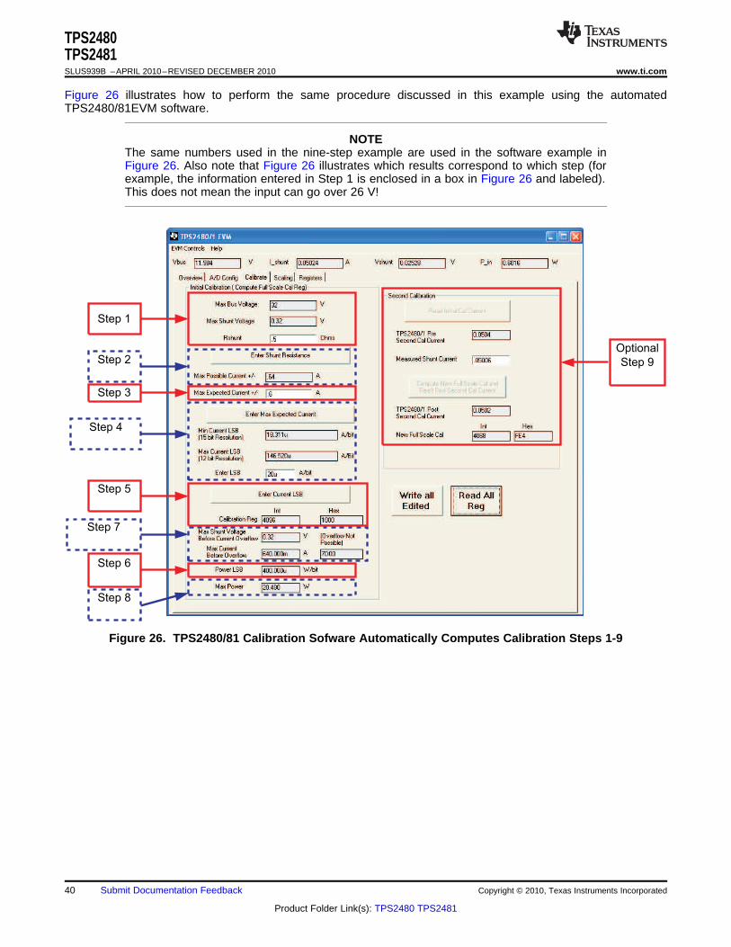
Step 1
Step 2
Step 3
Step 4
Step 5
Step 7
Step 6
Step 8
Optional
Step 9
TPS2480TPS2481SLUS939B –APRIL 2010–REVISED DECEMBER 2010 www.ti.com
Figure 26 illustrates how to perform the same procedure discussed in this example using the automatedTPS2480/81EVM software.
NOTEThe same numbers used in the nine-step example are used in the software example inFigure 26. Also note that Figure 26 illustrates which results correspond to which step (forexample, the information entered in Step 1 is enclosed in a box in Figure 26 and labeled).This does not mean the input can go over 26 V!
Figure 26. TPS2480/81 Calibration Sofware Automatically Computes Calibration Steps 1-9
40 Submit Documentation Feedback Copyright © 2010, Texas Instruments Incorporated
Product Folder Link(s): TPS2480 TPS2481

MaxPossible_I =V
RSHUNT_MAX
SHUNT
MaxPossible_I = 320
Minimum_LSB =Max_Expected_I
32767
Minimum_LSB = 1.831 10´ -3
Maximum_LSB =Max_Expected_I
4096
Maximum_LSB = 14.652 10´ -3
Cal = trunc0.04096
Current_LSB R´ SHUNT
Cal = 21557
Power_LSB = 20 Current_LSB´
Power_LSB = 38 10´-3
TPS2480TPS2481
www.ti.com SLUS939B –APRIL 2010–REVISED DECEMBER 2010
Calibration Example 2 (Overflow Possible)
This design example uses the nine-step procedure for calibrating the TPS2480/81 where overflow is possible.Figure 27 illustrates how the same procedure is performed using the automated TPS2480/81EVM software.
NOTE(The same numbers used in the nine-step example are used in the software example inFigure 27. Also note that Figure 27 illustrates which results correspond to which step (forexample, the information entered in Step 1 is circled in Figure 27 and labeled).
1. Establish the following parameters:
VBUS_MAX = 32, This does not mean the input can go over 26 V!
VSHUNT_MAX = 0.32
RSHUNT = 0.0012. Determine the maximum possible current using Equation 39:
(39)
3. Choose the desired maximum current value: Max_Expected_I, ≤ MaxPossible_I. This value is selectedbased on system expectations.
Max_Expected_I = 604. Calculate the possible range of current LSBs. This calculation is done by first computing a range of LSB's
that is appropriate for the design. Next, select an LSB withing this range. Note that the results will have themost resolution when the minimum LSB is selected. Typically, an LSB is selected to be the nearest roundnumber to the minimum LSB.
(40)
(41)
Choose an LSB in the range: Minimum_LSB<Selected_LSB<Maximum_LSB
Current_LSB = 1.9 × 10⁻³
NOTEThis value was selected to be a round number near the Minimum_LSB. This sectionallows for good resolution with a rounded LSB.
5. Compute the calibration register using Equation 42:
(42)
6. Calculate the Power LSB using Equation 43. Equation 43 shows a general formula; because the bus voltagemeasurement LSB is always 4mV, the power formula reduces to calculate the result.
(43)
Copyright © 2010, Texas Instruments Incorporated Submit Documentation Feedback 41
Product Folder Link(s): TPS2480 TPS2481

Max_Current = Current_LSB 32767´
Max_Current = 62.2573
Max_ShuntVoltage = Max_Current_Before_Overflow R´ SHUNT
Max_ShuntVoltage = 0.0622573
MaximumPower = Max_Current_Before_Overflow V´ BUS_MAX
MaximumPower = 1992
Corrected_Full_Scale_Cal = truncCal MeasShuntCurrent
TPS2480/81_Current
´
Corrected_Full_Scale_Cal = 21422
TPS2480TPS2481SLUS939B –APRIL 2010–REVISED DECEMBER 2010 www.ti.com
7. Compute the maximum current and shunt voltage values (before overflow), as shown by Equation 44 andEquation 45. Note that both Equation 44 and Equation 45 involve an If - then condition.
(44)
If Max_Current ≥ Max Possible_I thenMax_Current_Before_Overflow = MaxPossible_I
ElseMax_Current_Before_Overflow = Max_Current
End If
(Note that Max_Current is less than MaxPossible_I in this example.)
Max_Current_Before_Overflow = 62.2573 (Note: This result is displayed by software as seen in Figure 27.)
(45)
If Max_ShuntVoltage ≥ VSHUNT_MAX
Max_ShuntVoltage_Before_Overflow = VSHUNT_MAX
ElseMax_ShuntVoltage_Before_Overflow= Max_ShuntVoltage
End If(Note that Max_ShuntVoltage is less than VSHUNT_MAX in this example.)Max_ShuntVoltage_Before_Overflow = 0.0622573 (Note: This result is displayed by software as seen inFigure 27.)
8. Compute the maximum power with equation 8.
(46)
9. (Optional second calibration step.) Compute the corrected full-scale calibration value based on measuredcurrent.
TPS2480/81_Current = 25.2472
MeaShuntCurrent = 25.09
(47)
42 Submit Documentation Feedback Copyright © 2010, Texas Instruments Incorporated
Product Folder Link(s): TPS2480 TPS2481

Step 1
Step 2
Step 3
Step 4
Step 5
Step 7
Step 6
Step 8
Optional
Step 9
TPS2480TPS2481
www.ti.com SLUS939B –APRIL 2010–REVISED DECEMBER 2010
Figure 27 illustrates how to perform the same procedure discussed in this example using the automatedTPS2480/81EVM software.
NOTE(The same numbers used in the nine-step example are used in the software example inFigure 27. Also note that Figure 27 illustrates which results correspond to which step (forexample, the information entered in Step 1 is enclosed in a box in Figure 27 and labeled).
Figure 27. Calibration Software Automatically Computes Calibration Steps 1-9
Copyright © 2010, Texas Instruments Incorporated Submit Documentation Feedback 43
Product Folder Link(s): TPS2480 TPS2481
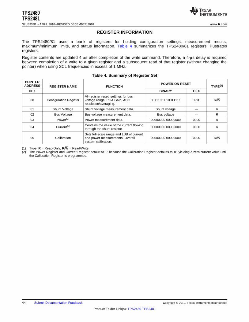
TPS2480TPS2481SLUS939B –APRIL 2010–REVISED DECEMBER 2010 www.ti.com
REGISTER INFORMATION
The TPS2480/81 uses a bank of registers for holding configuration settings, measurement results,maximum/minimum limits, and status information. Table 4 summarizes the TPS2480/81 registers; illustratesregisters.
Register contents are updated 4 ms after completion of the write command. Therefore, a 4-ms delay is requiredbetween completion of a write to a given register and a subsequent read of that register (without changing thepointer) when using SCL frequencies in excess of 1 MHz.
Table 4. Summary of Register Set
POINTER POWER-ON RESETADDRESS REGISTER NAME FUNCTION TYPE (1)
HEX BINARY HEX
All-register reset, settings for bus00 Configuration Register voltage range, PGA Gain, ADC 00111001 10011111 399F R/W
resolution/averaging.
01 Shunt Voltage Shunt voltage measurement data. Shunt voltage — R
02 Bus Voltage Bus voltage measurement data. Bus voltage — R
03 Power (2) Power measurement data. 00000000 00000000 0000 R
Contains the value of the current flowing04 Current (2) 00000000 00000000 0000 Rthrough the shunt resistor.
Sets full-scale range and LSB of current05 Calibration and power measurements. Overall 00000000 00000000 0000 R/W
system calibration.
(1) Type: R = Read-Only, R/W = Read/Write.(2) The Power Register and Current Register default to '0' because the Calibration Register defaults to '0', yielding a zero current value until
the Calibration Register is programmed.
44 Submit Documentation Feedback Copyright © 2010, Texas Instruments Incorporated
Product Folder Link(s): TPS2480 TPS2481

TPS2480TPS2481
www.ti.com SLUS939B –APRIL 2010–REVISED DECEMBER 2010
Register Details
All TPS2480/81 16-bit registers are actually two 8-bit registers.
Configuration Register 00h (Read/Write)BIT # D15 D14 D13 D12 D11 D10 D9 D8 D7 D6 D5 D4 D3 D2 D1 D0
BITRST — BRNG PG1 PG0 BADC4 BADC3 BADC2 BADC1 SADC4 SADC3 SADC2 SADC1 MODE3 MODE2 MODE1NAME
POR0 0 1 1 1 0 0 1 1 0 0 1 1 1 1 1VALUE
Bit Descriptions
RST: Reset Bit
Bit 15 Setting this bit to '1' generates a system reset that is the same as power-on reset. Resets all registers to defaultvalues; this bit self-clears.
BRNG: Bus Voltage Range
Bit 13 0 = 16-V FSR1 = 32-V FSR (default value)
PG: PGA (Shunt Voltage Only)
Bits 11, 12 Sets PGA gain and range. Note that the PGA defaults to ÷8 (320-mV range). Table 5 shows the gain and range forthe various product gain settings.
Table 5. PG Bit Settings (1)
PG1 PG0 GAIN RANGE
0 0 1 ±40 mV
0 1 ÷2 ±80 mV
1 0 ÷4 ±160 mV
1 1 ÷8 ±320 mV
(1) Shaded values are default.
BADC: BADC Bus ADC Resolution/Averaging
Bits 7–10 These bits adjust the Bus ADC resolution (9-, 10-, 11-, or 12-bit) or set the number of samples used whenaveraging results for the Bus Voltage Register (02h).
Copyright © 2010, Texas Instruments Incorporated Submit Documentation Feedback 45
Product Folder Link(s): TPS2480 TPS2481

TPS2480TPS2481SLUS939B –APRIL 2010–REVISED DECEMBER 2010 www.ti.com
SADC: SADC Shunt ADC Resolution/Averaging
Bits 3–6 These bits adjust the Shunt ADC resolution (9-, 10-, 11-, or 12-bit) or set the number of samples used whenaveraging results for the Shunt Voltage Register (01h).BADC (Bus) and SADC (Shunt) ADC resolution/averaging and conversion time settings are shown in Table 6.
Table 6. ADC Settings (1)
ADC4 ADC3 ADC2 ADC1 MODE/SAMPLES CONVERSION TIME
0 X (2) 0 0 9-bit 84 ms
0 X (2) 0 1 10-bit 148 ms
0 X (2) 1 0 11-bit 276 ms
0 X (2) 1 1 12-bit 532 ms
1 0 0 0 12-bit 532 ms
1 0 0 1 2 1.06 ms
1 0 1 0 4 2.13 ms
1 0 1 1 8 4.26 ms
1 1 0 0 16 8.51 ms
1 1 0 1 32 17.02 ms
1 1 1 0 64 34.05 ms
1 1 1 1 128 68.10 ms
(1) Shaded values are default.(2) X = Don't care.
MODE: Operating Mode
Bits 0–2 Selects continuous, triggered, or power-down mode of operation. These bits default to continuous shunt and busmeasurement mode. The mode settings are shown in Table 7.
Table 7. Mode Settings (1)
MODE3 MODE2 MODE1 MODE
0 0 0 Power-down
0 0 1 Shunt voltage, triggered
0 1 0 Bus voltage, triggered
0 1 1 Shunt and bus, triggered
1 0 0 ADC off (disabled)
1 0 1 Shunt voltage, continuous
1 1 0 Bus voltage, continuous
1 1 1 Shunt and bus, continuous
(1) Shaded values are default.
46 Submit Documentation Feedback Copyright © 2010, Texas Instruments Incorporated
Product Folder Link(s): TPS2480 TPS2481

TPS2480TPS2481
www.ti.com SLUS939B –APRIL 2010–REVISED DECEMBER 2010
Data Output Registers
Shunt Voltage Register 01h (Read-Only)
The Shunt Voltage Register stores the current shunt voltage reading, VSHUNT. Shunt Voltage Register bits areshifted according to the PGA setting selected in the Configuration Register (00h). When multiple sign bits arepresent, they will all be the same value. Negative numbers are represented in two's complement format.Generate the two's complement of a negative number by complementing the absolute value binary number andadding 1. Extend the sign, denoting a negative number by setting the MSB = '1'. Extend the sign to anyadditional sign bits to form the 16-bit word.
Example: For a value of VSHUNT = –320 mV:1. Take the absolute value (include accuracy to 0.01mV)==> 320.002. Translate this number to a whole decimal number ==> 320003. Convert it to binary==> 111 1101 0000 00004. Complement the binary result : 000 0010 1111 11115. Add 1 to the Complement to create the Two’s Complement formatted result ==> 000 0011 0000 00006. Extend the sign and create the 16-bit word: 1000 0011 0000 0000 = 8300h (Remember to extend the sign to
all sign-bits, as necessary based on the PGA setting.)
At PGA = ÷8, full-scale range = ±320 mV (decimal = 32000, positive value hex = 7D00, negative value hex =8300), and LSB = 10 mV.
BIT # D15 D14 D13 D12 D11 D10 D9 D8 D7 D6 D5 D4 D3 D2 D1 D0
BITSIGN SD14_8 SD13_8 SD12_8 SD11_8 SD10_8 SD9_8 SD8_8 SD7_8 SD6_8 SD5_8 SD4_8 SD3_8 SD2_8 SD1_8 SD0_8NAME
POR0 0 0 0 0 0 0 0 0 0 0 0 0 0 0 0VALUE
At PGA = ÷4, full-scale range = ±160 mV (decimal = 16000, positive value hex = 3E80, negative value hex =C180), and LSB = 10 mV.
BIT # D15 D14 D13 D12 D11 D10 D9 D8 D7 D6 D5 D4 D3 D2 D1 D0
BITSIGN SIGN SD13_4 SD12_4 SD11_4 SD10_4 SD9_4 SD8_4 SD7_4 SD6_4 SD5_4 SD4_4 SD3_4 SD2_4 SD1_4 SD0_4NAME
POR0 0 0 0 0 0 0 0 0 0 0 0 0 0 0 0VALUE
At PGA = ÷2, full-scale range = ±80 mV (decimal = 8000, positive value hex = 1F40, negative value hex =E0C0), and LSB = 10 mV.
BIT # D15 D14 D13 D12 D11 D10 D9 D8 D7 D6 D5 D4 D3 D2 D1 D0
BITSIGN SIGN SIGN SD12_2 SD11_2 SD10_2 SD9_2 SD8_2 SD7_2 SD6_2 SD5_2 SD4_2 SD3_2 SD2_2 SD1_2 SD0_2NAME
POR0 0 0 0 0 0 0 0 0 0 0 0 0 0 0 0VALUE
At PGA = ÷1, full-scale range = ±40 mV (decimal = 4000, positive value hex = 0FA0, negative value hex = F060),and LSB = 10 mV.
BIT # D15 D14 D13 D12 D11 D10 D9 D8 D7 D6 D5 D4 D3 D2 D1 D0
BITSIGN SIGN SIGN SIGN SD11_1 SD10_1 SD9_1 SD8_1 SD7_1 SD6_1 SD5_1 SD4_1 SD3_1 SD2_1 SD1_1 SD0_1NAME
POR0 0 0 0 0 0 0 0 0 0 0 0 0 0 0 0VALUE
Copyright © 2010, Texas Instruments Incorporated Submit Documentation Feedback 47
Product Folder Link(s): TPS2480 TPS2481

TPS2480TPS2481SLUS939B –APRIL 2010–REVISED DECEMBER 2010 www.ti.com
Table 8. Shunt Voltage Register Format (1)
VSHUNT Decimal PGA = ÷ 8 PGA = ÷ 4 PGA = ÷ 2 PGA = ÷ 1Reading (mV) Value (D15…..................D0) (D15…..................D0) (D15…..................D0) (D15…..................D0)
320.02 32002 0111 1101 0000 0000 0011 1110 1000 0000 0001 1111 0100 0000 0000 1111 1010 0000
320.01 32001 0111 1101 0000 0000 0011 1110 1000 0000 0001 1111 0100 0000 0000 1111 1010 0000
320.00 32000 0111 1101 0000 0000 0011 1110 1000 0000 0001 1111 0100 0000 0000 1111 1010 0000
319.99 31999 0111 1100 1111 1111 0011 1110 1000 0000 0001 1111 0100 0000 0000 1111 1010 0000
319.98 31998 0111 1100 1111 1110 0011 1110 1000 0000 0001 1111 0100 0000 0000 1111 1010 0000
- - - - - -
160.02 16002 0011 1110 1000 0010 0011 1110 1000 0000 0001 1111 0100 0000 0000 1111 1010 0000
160.01 16001 0011 1110 1000 0001 0011 1110 1000 0000 0001 1111 0100 0000 0000 1111 1010 0000
160.00 16000 0011 1110 1000 0000 0011 1110 1000 0000 0001 1111 0100 0000 0000 1111 1010 0000
159.99 15999 0011 1110 0111 1111 0011 1110 0111 1111 0001 1111 0100 0000 0000 1111 1010 0000
159.98 15998 0011 1110 0111 1110 0011 1110 0111 1110 0001 1111 0100 0000 0000 1111 1010 0000
- - - - - -
80.02 8002 0001 1111 0100 0010 0001 1111 0100 0010 0001 1111 0100 0000 0000 1111 1010 0000
80.01 8001 0001 1111 0100 0001 0001 1111 0100 0001 0001 1111 0100 0000 0000 1111 1010 0000
80.00 8000 0001 1111 0100 0000 0001 1111 0100 0000 0001 1111 0100 0000 0000 1111 1010 0000
79.99 7999 0001 1111 0011 1111 0001 1111 0011 1111 0001 1111 0011 1111 0000 1111 1010 0000
79.98 7998 0001 1111 0011 1110 0001 1111 0011 1110 0001 1111 0011 1110 0000 1111 1010 0000
- - - - - -
40.02 4002 0000 1111 1010 0010 0000 1111 1010 0010 0000 1111 1010 0010 0000 1111 1010 0000
40.01 4001 0000 1111 1010 0001 0000 1111 1010 0001 0000 1111 1010 0001 0000 1111 1010 0000
40.00 4000 0000 1111 1010 0000 0000 1111 1010 0000 0000 1111 1010 0000 0000 1111 1010 0000
39.99 3999 0000 1111 1001 1111 0000 1111 1001 1111 0000 1111 1001 1111 0000 1111 1001 1111
39.98 3998 0000 1111 1001 1110 0000 1111 1001 1110 0000 1111 1001 1110 0000 1111 1001 1110
- - - - - -
0.02 2 0000 0000 0000 0010 0000 0000 0000 0010 0000 0000 0000 0010 0000 0000 0000 0010
0.01 1 0000 0000 0000 0001 0000 0000 0000 0001 0000 0000 0000 0001 0000 0000 0000 0001
0 0 0000 0000 0000 0000 0000 0000 0000 0000 0000 0000 0000 0000 0000 0000 0000 0000
–0.01 –1 1111 1111 1111 1111 1111 1111 1111 1111 1111 1111 1111 1111 1111 1111 1111 1111
–0.02 –2 1111 1111 1111 1110 1111 1111 1111 1110 1111 1111 1111 1110 1111 1111 1111 1110
- - - - - -
–39.98 –3998 1111 0000 0110 0010 1111 0000 0110 0010 1111 0000 0110 0010 1111 0000 0110 0010
–39.99 –3999 1111 0000 0110 0001 1111 0000 0110 0001 1111 0000 0110 0001 1111 0000 0110 0001
–40.00 –4000 1111 0000 0110 0000 1111 0000 0110 0000 1111 0000 0110 0000 1111 0000 0110 0000
–40.01 –4001 1111 0000 0101 1111 1111 0000 0101 1111 1111 0000 0101 1111 1111 0000 0110 0000
–40.02 –4002 1111 0000 0101 1110 1111 0000 0101 1110 1111 0000 0101 1110 1111 0000 0110 0000
- - - - - -
–79.98 –7998 1110 0000 1100 0010 1110 0000 1100 0010 1110 0000 1100 0010 1111 0000 0110 0000
–79.99 –7999 1110 0000 1100 0001 1110 0000 1100 0001 1110 0000 1100 0001 1111 0000 0110 0000
–80.00 –8000 1110 0000 1100 0000 1110 0000 1100 0000 1110 0000 1100 0000 1111 0000 0110 0000
–80.01 –8001 1110 0000 1011 1111 1110 0000 1011 1111 1110 0000 1100 0000 1111 0000 0110 0000
–80.02 –8002 1110 0000 1011 1110 1110 0000 1011 1110 1110 0000 1100 0000 1111 0000 0110 0000
- - - - - -
–159.98 –15998 1100 0001 1000 0010 1100 0001 1000 0010 1110 0000 1100 0000 1111 0000 0110 0000
–159.99 –15999 1100 0001 1000 0001 1100 0001 1000 0001 1110 0000 1100 0000 1111 0000 0110 0000
–160.00 –16000 1100 0001 1000 0000 1100 0001 1000 0000 1110 0000 1100 0000 1111 0000 0110 0000
–160.01 –16001 1100 0001 0111 1111 1100 0001 1000 0000 1110 0000 1100 0000 1111 0000 0110 0000
–160.02 –16002 1100 0001 0111 1110 1100 0001 1000 0000 1110 0000 1100 0000 1111 0000 0110 0000
- - - - - -
–319.98 –31998 1000 0011 0000 0010 1100 0001 1000 0000 1110 0000 1100 0000 1111 0000 0110 0000
–319.99 –31999 1000 0011 0000 0001 1100 0001 1000 0000 1110 0000 1100 0000 1111 0000 0110 0000
–320.00 –32000 1000 0011 0000 0000 1100 0001 1000 0000 1110 0000 1100 0000 1111 0000 0110 0000
–320.01 –32001 1000 0011 0000 0000 1100 0001 1000 0000 1110 0000 1100 0000 1111 0000 0110 0000
–320.02 –32002 1000 0011 0000 0000 1100 0001 1000 0000 1110 0000 1100 0000 1111 0000 0110 0000
(1) Out-of-range values are shown in grey shading.
48 Submit Documentation Feedback Copyright © 2010, Texas Instruments Incorporated
Product Folder Link(s): TPS2480 TPS2481

Power =Current BusVoltage´
5000
TPS2480TPS2481
www.ti.com SLUS939B –APRIL 2010–REVISED DECEMBER 2010
Bus Voltage Register 02h (Read-Only)
The Bus Voltage Register stores the most recent bus voltage reading, VBUS.
At full-scale range = 32 V (decimal = 8000, hex = 1F40), and LSB = 4 mV.
BIT # D15 D14 D13 D12 D11 D10 D9 D8 D7 D6 D5 D4 D3 D2 D1 D0
BITBD12 BD11 BD10 BD9 BD8 BD7 BD6 BD5 BD4 BD3 BD2 BD1 BD0 — CNVR OVFNAME
POR0 0 0 0 0 0 0 0 0 0 0 0 0 0 0 0VALUE
At full-scale range = 16 V (decimal = 4000, hex = 0FA0), and LSB = 4 mV.
BIT # D15 D14 D13 D12 D11 D10 D9 D8 D7 D6 D5 D4 D3 D2 D1 D0
BIT0 BD11 BD10 BD9 BD8 BD7 BD6 BD5 BD4 BD3 BD2 BD1 BD0 — CNVR OVFNAME
POR0 0 0 0 0 0 0 0 0 0 0 0 0 0 0 0VALUE
CNVR: Conversion Ready
Bit 1 Although the data from the last conversion can be read at any time, the TPS2480/81 Conversion Ready bit (CNVR)indicates when data from a conversion is available in the data output registers. The CNVR bit is set after allconversions, averaging, and multiplications are complete. CNVR will clear under the following conditions:
1) Writing a new mode into the Operating Mode bits in the Configuration Register (except for Power-Down orDisable)
2.) Reading the Power Register
OVF: Math Overflow Flag
Bit 0 The Math Overflow Flag (OVF) is set when the Power or Current calculations are out of range. It indicates thatcurrent and power data may be meaningless.
Power Register 03h (Read-Only)
Full-scale range and LSB are set by the Calibration Register. See the TPS2480/81 Power Measurement Enginesection.
BIT # D15 D14 D13 D12 D11 D10 D9 D8 D7 D6 D5 D4 D3 D2 D1 D0
BITPD15 PD14 PD13 PD12 PD11 PD10 PD9 PD8 PD7 PD6 PD5 PD4 PD3 PD2 PD1 PD0NAME
POR0 0 0 0 0 0 0 0 0 0 0 0 0 0 0 0VALUE
The Power Register records power in watts by multiplying the values of the current with the value of the busvoltage according to the equation:
Copyright © 2010, Texas Instruments Incorporated Submit Documentation Feedback 49
Product Folder Link(s): TPS2480 TPS2481

Current =ShuntVoltage Calibration Register´
4096
TPS2480TPS2481SLUS939B –APRIL 2010–REVISED DECEMBER 2010 www.ti.com
Current Register 04h (Read-Only)
Full-scale range and LSB depend on the value entered in the Calibration Register. See the TPS2480/81 PowerMeasurement Engine section. Negative values are stored in two's complement format.
BIT # D15 D14 D13 D12 D11 D10 D9 D8 D7 D6 D5 D4 D3 D2 D1 D0
BITCSIGN CD14 CD13 CD12 CD11 CD10 CD9 CD8 CD7 CD6 CD5 CD4 CD3 CD2 CD1 CD0NAME
POR0 0 0 0 0 0 0 0 0 0 0 0 0 0 0 0VALUE
The value of the Current Register is calculated by multiplying the value in the Shunt Voltage Register with thevalue in the Calibration Register according to the equation:
Calibration Register
Calibration Register 05h (Read/Write)
Current and power calibration are set by bits D15 to D1 of the Calibration Register. Note that bit D0 is not used inthe calculation. This register sets the current that corresponds to a full-scale drop across the shunt. Full-scalerange and the LSB of the current and power measurement depend on the value entered in this register. See theTPS2480/81 Power Measurement Engine section. This register is suitable for use in overall system calibration.Note that the '0' POR values are all default.
BIT # D15 D14 D13 D12 D11 D10 D9 D8 D7 D6 D5 D4 D3 D2 D1 D0 (1)
BITFS15 FS14 FS13 FS12 FS11 FS10 FS9 FS8 FS7 FS6 FS5 FS4 FS3 FS2 FS1 FS0NAME
POR0 0 0 0 0 0 0 0 0 0 0 0 0 0 0 0VALUE
(1) D0 is a void bit and will always be '0'. It is not possible to write a '1' to D0. CALIBRATION is the value stored in D15:D1.
50 Submit Documentation Feedback Copyright © 2010, Texas Instruments Incorporated
Product Folder Link(s): TPS2480 TPS2481

TPS2480TPS2481
www.ti.com SLUS939B –APRIL 2010–REVISED DECEMBER 2010
REVISION HISTORY
Changes from Revision A (April, 2010) to Revision B Page
• Changed Increased the input range from 20-V to 26-V ........................................................................................................ 1
• Changed Simplified Application Diagram drawing on the first page. .................................................................................... 1
• Added Function column to the DEVICE INFORMATION Table. .......................................................................................... 2
• Changed RECOMMENDED OPERATING CONDITIONS Input Voltage range increase to 24.5 V. .................................... 2
• Added split Input bias current row and updated values. ....................................................................................................... 6
• Changed Design Example Schematic drawing. .................................................................................................................. 20
• Changed Figure 17 TPS2480/81 Low Voltage Design Example Schematic drawing ........................................................ 20
• Changed High Voltage Application drawing. ...................................................................................................................... 25
• Changed Figure 19 TPS2480/81 High Voltage Application drawing .................................................................................. 25
• Added Input Transient Protectionsection. ........................................................................................................................... 26
Copyright © 2010, Texas Instruments Incorporated Submit Documentation Feedback 51
Product Folder Link(s): TPS2480 TPS2481

PACKAGE OPTION ADDENDUM
www.ti.com 9-Sep-2014
Addendum-Page 1
PACKAGING INFORMATION
Orderable Device Status(1)
Package Type PackageDrawing
Pins PackageQty
Eco Plan(2)
Lead/Ball Finish(6)
MSL Peak Temp(3)
Op Temp (°C) Device Marking(4/5)
Samples
TPS2480PW ACTIVE TSSOP PW 20 70 Green (RoHS& no Sb/Br)
CU NIPDAU Level-1-260C-UNLIM -40 to 125 TPS2480
TPS2480PWR ACTIVE TSSOP PW 20 2000 Green (RoHS& no Sb/Br)
CU NIPDAU Level-1-260C-UNLIM -40 to 125 TPS2480
TPS2481PW ACTIVE TSSOP PW 20 70 Green (RoHS& no Sb/Br)
CU NIPDAU Level-1-260C-UNLIM -40 to 125 TPS2481
TPS2481PWR ACTIVE TSSOP PW 20 2000 Green (RoHS& no Sb/Br)
CU NIPDAU Level-1-260C-UNLIM -40 to 125 TPS2481
(1) The marketing status values are defined as follows:ACTIVE: Product device recommended for new designs.LIFEBUY: TI has announced that the device will be discontinued, and a lifetime-buy period is in effect.NRND: Not recommended for new designs. Device is in production to support existing customers, but TI does not recommend using this part in a new design.PREVIEW: Device has been announced but is not in production. Samples may or may not be available.OBSOLETE: TI has discontinued the production of the device.
(2) Eco Plan - The planned eco-friendly classification: Pb-Free (RoHS), Pb-Free (RoHS Exempt), or Green (RoHS & no Sb/Br) - please check http://www.ti.com/productcontent for the latest availabilityinformation and additional product content details.TBD: The Pb-Free/Green conversion plan has not been defined.Pb-Free (RoHS): TI's terms "Lead-Free" or "Pb-Free" mean semiconductor products that are compatible with the current RoHS requirements for all 6 substances, including the requirement thatlead not exceed 0.1% by weight in homogeneous materials. Where designed to be soldered at high temperatures, TI Pb-Free products are suitable for use in specified lead-free processes.Pb-Free (RoHS Exempt): This component has a RoHS exemption for either 1) lead-based flip-chip solder bumps used between the die and package, or 2) lead-based die adhesive used betweenthe die and leadframe. The component is otherwise considered Pb-Free (RoHS compatible) as defined above.Green (RoHS & no Sb/Br): TI defines "Green" to mean Pb-Free (RoHS compatible), and free of Bromine (Br) and Antimony (Sb) based flame retardants (Br or Sb do not exceed 0.1% by weightin homogeneous material)
(3) MSL, Peak Temp. - The Moisture Sensitivity Level rating according to the JEDEC industry standard classifications, and peak solder temperature.
(4) There may be additional marking, which relates to the logo, the lot trace code information, or the environmental category on the device.
(5) Multiple Device Markings will be inside parentheses. Only one Device Marking contained in parentheses and separated by a "~" will appear on a device. If a line is indented then it is a continuationof the previous line and the two combined represent the entire Device Marking for that device.
(6) Lead/Ball Finish - Orderable Devices may have multiple material finish options. Finish options are separated by a vertical ruled line. Lead/Ball Finish values may wrap to two lines if the finishvalue exceeds the maximum column width.

PACKAGE OPTION ADDENDUM
www.ti.com 9-Sep-2014
Addendum-Page 2
Important Information and Disclaimer:The information provided on this page represents TI's knowledge and belief as of the date that it is provided. TI bases its knowledge and belief on informationprovided by third parties, and makes no representation or warranty as to the accuracy of such information. Efforts are underway to better integrate information from third parties. TI has taken andcontinues to take reasonable steps to provide representative and accurate information but may not have conducted destructive testing or chemical analysis on incoming materials and chemicals.TI and TI suppliers consider certain information to be proprietary, and thus CAS numbers and other limited information may not be available for release.
In no event shall TI's liability arising out of such information exceed the total purchase price of the TI part(s) at issue in this document sold by TI to Customer on an annual basis.

TAPE AND REEL INFORMATION
*All dimensions are nominal
Device PackageType
PackageDrawing
Pins SPQ ReelDiameter
(mm)
ReelWidth
W1 (mm)
A0(mm)
B0(mm)
K0(mm)
P1(mm)
W(mm)
Pin1Quadrant
TPS2480PWR TSSOP PW 20 2000 330.0 16.4 6.95 7.1 1.6 8.0 16.0 Q1
TPS2481PWR TSSOP PW 20 2000 330.0 16.4 6.95 7.1 1.6 8.0 16.0 Q1
PACKAGE MATERIALS INFORMATION
www.ti.com 14-Jul-2012
Pack Materials-Page 1

*All dimensions are nominal
Device Package Type Package Drawing Pins SPQ Length (mm) Width (mm) Height (mm)
TPS2480PWR TSSOP PW 20 2000 367.0 367.0 38.0
TPS2481PWR TSSOP PW 20 2000 367.0 367.0 38.0
PACKAGE MATERIALS INFORMATION
www.ti.com 14-Jul-2012
Pack Materials-Page 2


IMPORTANT NOTICE
Texas Instruments Incorporated and its subsidiaries (TI) reserve the right to make corrections, enhancements, improvements and otherchanges to its semiconductor products and services per JESD46, latest issue, and to discontinue any product or service per JESD48, latestissue. Buyers should obtain the latest relevant information before placing orders and should verify that such information is current andcomplete. All semiconductor products (also referred to herein as “components”) are sold subject to TI’s terms and conditions of salesupplied at the time of order acknowledgment.TI warrants performance of its components to the specifications applicable at the time of sale, in accordance with the warranty in TI’s termsand conditions of sale of semiconductor products. Testing and other quality control techniques are used to the extent TI deems necessaryto support this warranty. Except where mandated by applicable law, testing of all parameters of each component is not necessarilyperformed.TI assumes no liability for applications assistance or the design of Buyers’ products. Buyers are responsible for their products andapplications using TI components. To minimize the risks associated with Buyers’ products and applications, Buyers should provideadequate design and operating safeguards.TI does not warrant or represent that any license, either express or implied, is granted under any patent right, copyright, mask work right, orother intellectual property right relating to any combination, machine, or process in which TI components or services are used. Informationpublished by TI regarding third-party products or services does not constitute a license to use such products or services or a warranty orendorsement thereof. Use of such information may require a license from a third party under the patents or other intellectual property of thethird party, or a license from TI under the patents or other intellectual property of TI.Reproduction of significant portions of TI information in TI data books or data sheets is permissible only if reproduction is without alterationand is accompanied by all associated warranties, conditions, limitations, and notices. TI is not responsible or liable for such altereddocumentation. Information of third parties may be subject to additional restrictions.Resale of TI components or services with statements different from or beyond the parameters stated by TI for that component or servicevoids all express and any implied warranties for the associated TI component or service and is an unfair and deceptive business practice.TI is not responsible or liable for any such statements.Buyer acknowledges and agrees that it is solely responsible for compliance with all legal, regulatory and safety-related requirementsconcerning its products, and any use of TI components in its applications, notwithstanding any applications-related information or supportthat may be provided by TI. Buyer represents and agrees that it has all the necessary expertise to create and implement safeguards whichanticipate dangerous consequences of failures, monitor failures and their consequences, lessen the likelihood of failures that might causeharm and take appropriate remedial actions. Buyer will fully indemnify TI and its representatives against any damages arising out of the useof any TI components in safety-critical applications.In some cases, TI components may be promoted specifically to facilitate safety-related applications. With such components, TI’s goal is tohelp enable customers to design and create their own end-product solutions that meet applicable functional safety standards andrequirements. Nonetheless, such components are subject to these terms.No TI components are authorized for use in FDA Class III (or similar life-critical medical equipment) unless authorized officers of the partieshave executed a special agreement specifically governing such use.Only those TI components which TI has specifically designated as military grade or “enhanced plastic” are designed and intended for use inmilitary/aerospace applications or environments. Buyer acknowledges and agrees that any military or aerospace use of TI componentswhich have not been so designated is solely at the Buyer's risk, and that Buyer is solely responsible for compliance with all legal andregulatory requirements in connection with such use.TI has specifically designated certain components as meeting ISO/TS16949 requirements, mainly for automotive use. In any case of use ofnon-designated products, TI will not be responsible for any failure to meet ISO/TS16949.
Products ApplicationsAudio www.ti.com/audio Automotive and Transportation www.ti.com/automotiveAmplifiers amplifier.ti.com Communications and Telecom www.ti.com/communicationsData Converters dataconverter.ti.com Computers and Peripherals www.ti.com/computersDLP® Products www.dlp.com Consumer Electronics www.ti.com/consumer-appsDSP dsp.ti.com Energy and Lighting www.ti.com/energyClocks and Timers www.ti.com/clocks Industrial www.ti.com/industrialInterface interface.ti.com Medical www.ti.com/medicalLogic logic.ti.com Security www.ti.com/securityPower Mgmt power.ti.com Space, Avionics and Defense www.ti.com/space-avionics-defenseMicrocontrollers microcontroller.ti.com Video and Imaging www.ti.com/videoRFID www.ti-rfid.comOMAP Applications Processors www.ti.com/omap TI E2E Community e2e.ti.comWireless Connectivity www.ti.com/wirelessconnectivity
Mailing Address: Texas Instruments, Post Office Box 655303, Dallas, Texas 75265Copyright © 2015, Texas Instruments Incorporated

![Title 51 RCW - Washingtonleg.wa.gov › CodeReviser › RCWArchive › Documents › 2018 › Title 51...(2018 Ed.) [Title 51 RCW—page 1] Title 51 Title 51 51 INDUSTRIAL INSURANCE](https://img.pdfslide.us/doc/110x75/5f13739b25d6831c263b508b/title-51-rcw-a-codereviser-a-rcwarchive-a-documents-a-2018-a-title-51.jpg)

![lawfilesext.leg.wa.govlawfilesext.leg.wa.gov/law/WACArchive/2018a/WAC 51 - 51 CHAPTE… · 51-51-003 2015 International Residential Code [Ch. 51-51 WAC p. 2] (5/6/16) mation, and](https://img.pdfslide.us/doc/110x75/5fe0b6b2b6ec272d7d49e8b5/51-51-chapte-51-51-003-2015-international-residential-code-ch-51-51-wac-p.jpg)