Embed Size (px)
Citation preview

ELG4139: Oscillator Circuits
Positive Feedback Amplifiers (Oscillators)
LC and Crystal Oscillators
JBT; FET; and IC Based Oscillators
The Active-Filter-Tuned Oscillator
Multivibrators
1

Introduction
• There are two different approaches for the generation of sinusoids, most commonly used for the standard waveforms:
– Employing a positive-feedback loop that consists an amplifier and an RC or LC frequency-selective network. It generates sine waves utilizing resonance phenomena, are known as linear oscillators (circuits that generate square, triangular, pulse waveforms are called non-linear oscillators or function generators.)
– A sine wave is obtained by appropriate shaping a triangular waveform.
2

The Oscillator Feedback Loop A basic structure of a sinusoidal oscillator consists of an amplifier and a frequency-
selective network connected in a positive-feedback loop.
The condition for the feedback loop to provide sinusoidal oscillations of
frequency w0 is
Barkhausen Criterion:
At w0 the phase of the loop gain should be zero.
At w0 the magnitude of the loop gain should be unity.

(a) Colpitts and (b) Hartley.
LC and Crystal Oscillators For higher frequencies (> 1MHz)
CLLwo
)21(
1
)21
21(
1
CC
CCL
wo

Hartley Oscillator Used in radio receivers and transmitters More stable than Armstrong
oscillators Radio frequency choke (RFC)
21
210
&
22
1
LLbetweencouplingMutualM
MLLLwhereCL
feq
eq
L1 L2
C
Colpitts Oscillators BJT; FET; and IC Based
-
Rf
Ri
21
21
02
1
CC
CCCwhere
LCf
eq
eq
LC network LC network
C1 C1 C2 C2
RFC is an impedance which is high (open) at high RF frequencies and low (short) to dc voltages

Equivalent Circuit of the Colpitts Oscillator
)21
21(
1
CC
CCL
wo
Complete Circuit for a Colpitts Oscillator
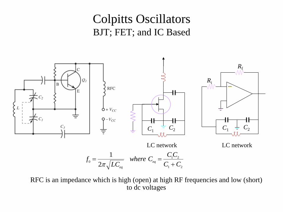
Crystal Oscillators
8
Radio communications, broadcasting stations
Piezoelectric effect
Why are crystal oscillators used in many commercial
transmitters?
Crystal is a piezo-electric device which converts mechanical pressure to electrical voltage or vice-vasa
LCffrequencySeries
S
S
2
1
LCC
CCffrequencyParallel
PS
PS
P
2
1
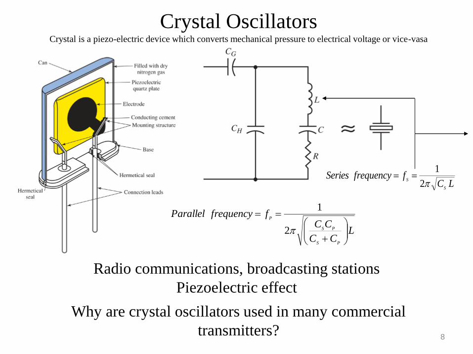
An Application of Crystal Oscillator
9
Two crystals producing two different frequencies for measuring
temperature Timing devices
Crystals are fabricated by cutting the crude quartz in a very exacting
fashion. The type of cut determines the crystal’s natural resonant frequency
as well as it’s temperature coefficient.
Crystal are available at frequencies about 15kHz and up providing the
best frequency stability. However above 100MHz, they become so small
that handling becomes a problem.
10
Op-amp
-
+
R2 Cs
Vz
Rf
R1
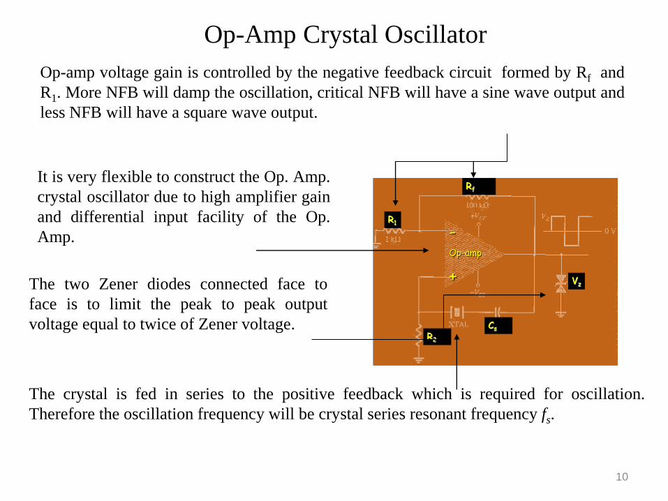
Op-Amp Crystal Oscillator
Op-amp voltage gain is controlled by the negative feedback circuit formed by Rf and
R1. More NFB will damp the oscillation, critical NFB will have a sine wave output and
less NFB will have a square wave output.
The two Zener diodes connected face to
face is to limit the peak to peak output
voltage equal to twice of Zener voltage.
It is very flexible to construct the Op. Amp.
crystal oscillator due to high amplifier gain
and differential input facility of the Op.
Amp.
The crystal is fed in series to the positive feedback which is required for oscillation.
Therefore the oscillation frequency will be crystal series resonant frequency fs.

Example
11
Crystal used instead of inductor in the tank
circuit of Colpitts oscillator
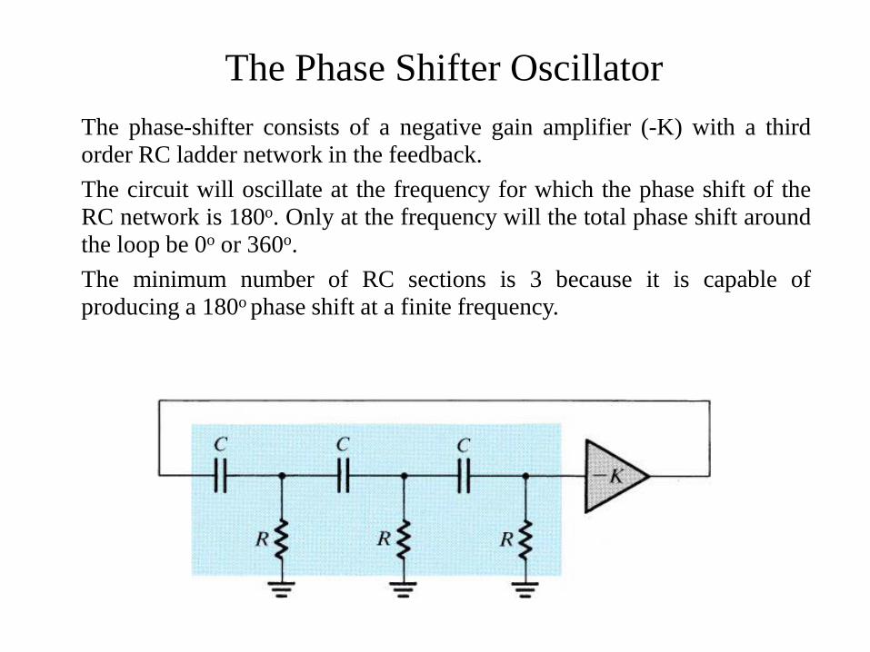
The Phase Shifter Oscillator
The phase-shifter consists of a negative gain amplifier (-K) with a third
order RC ladder network in the feedback.
The circuit will oscillate at the frequency for which the phase shift of the
RC network is 180o. Only at the frequency will the total phase shift around
the loop be 0o or 360o.
The minimum number of RC sections is 3 because it is capable of
producing a 180o phase shift at a finite frequency.
bAVi = Vi (or) Ab =1
A Vi
AVi bAVi
b R
C
R R
C C
Phase-shift Oscillator
C
RD= ?
VDD
R
R
C R
C= ?
-
kkk
kkRkkRrRRBut
kSg
RRgAALetA
DDdDL
m
LLm
10840
408840////
85000
40404029401
b
nFkkRf
CRC
f 5.661102
1
62
1
62
1
f = 1kHz
rd= 40k gm= 5000mS R=10k
FET Phase-shift Oscillator
Example:
Determine the value of capacitance C and the
value of RD of the Phase-shift oscillator
shown, if the output frequency is 1 kHz. Take
rd = 40k and
gm=5000mS, for the FET and R = 10kW.
A
b
62
1
RCf
Frequency of oscillation
29
1b
29
1
A
Ab
Condition of oscillation
14
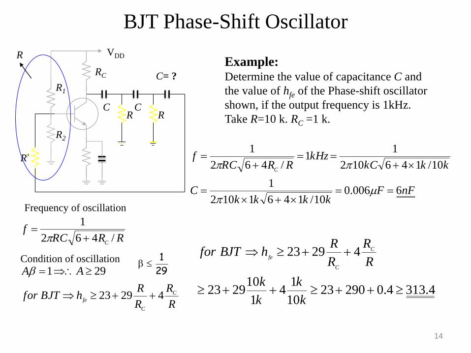
BJT Phase-Shift Oscillator
C
VDD
R2
R
C R
C= ? RC
R1
R’
R Example: Determine the value of capacitance C and
the value of hfe of the Phase-shift oscillator
shown, if the output frequency is 1kHz.
Take R=10 k. RC =1 k.
nFFkkkk
C
kkkCkHz
RRRCf
C
6006.010/1461102
1
10/146102
11
/462
1
4.3134.02902310
14
1
102923
42923
k
k
k
k
R
R
R
RhBJTfor C
C
fe
RRRCf
C/462
1
Frequency of oscillation
R
R
R
RhBJTfor
AA
C
C
fe42923
291
b 29
1bCondition of oscillation
15
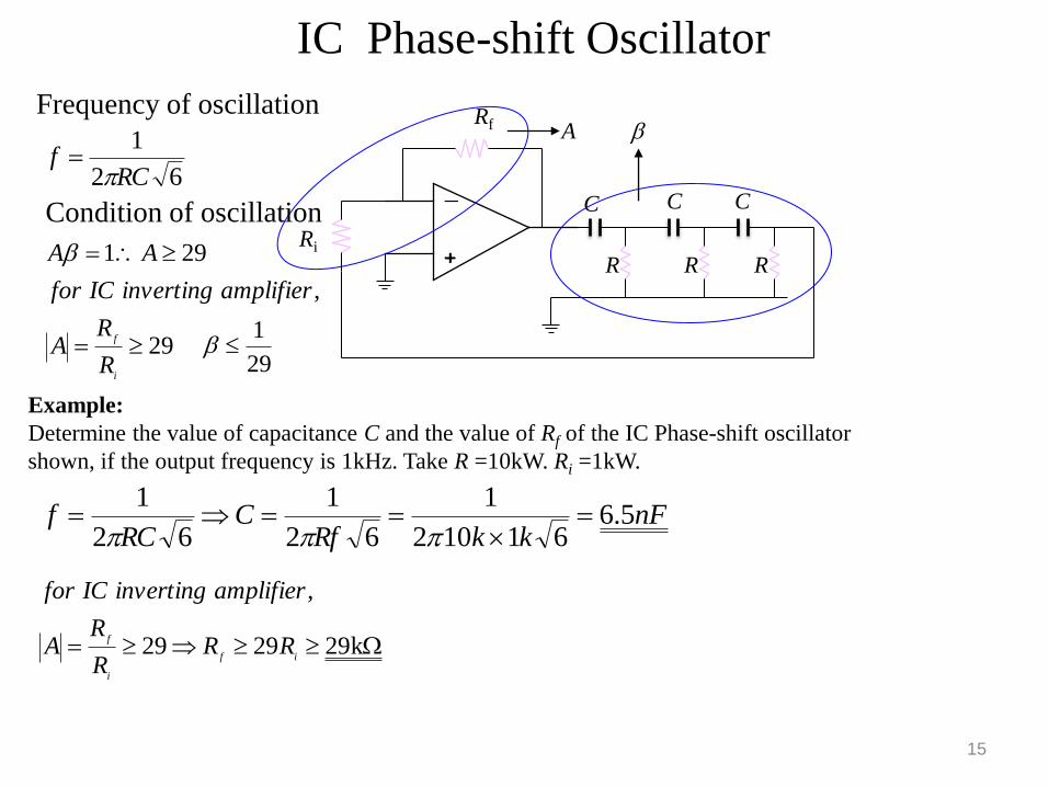
IC Phase-shift Oscillator
R
C
+
-
R
C
R
C
Rf
Ri
Example:
Determine the value of capacitance C and the value of Rf of the IC Phase-shift oscillator
shown, if the output frequency is 1kHz. Take R =10kW. Ri =1kW.
nFkkRf
CRC
f 5.661102
1
62
1
62
1
k292929
,
if
i
fRR
R
RA
amplifierinvertingICfor
A b
62
1
RCf
Frequency of oscillation
29
,
291
i
f
R
RA
amplifierinvertingICfor
AAb
29
1b
Condition of oscillation
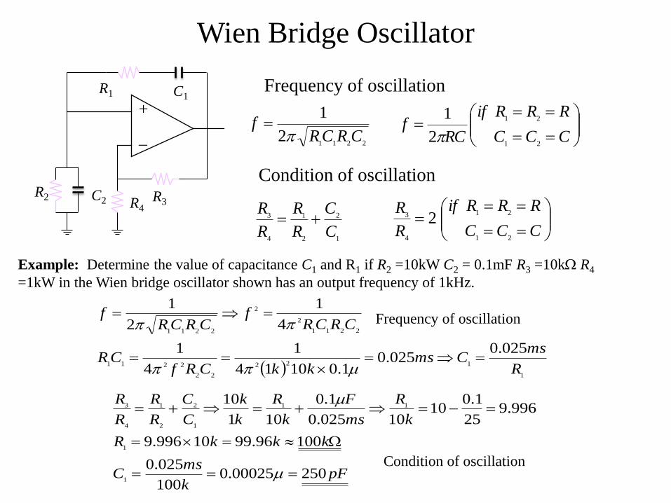
Wien Bridge Oscillator
+
-
R1 C1
R3 R4
R2 C2
22112
1
CRCRf
CCC
RRRif
RCf
21
21
2
1
Frequency of oscillation
1
2
2
1
4
3
C
C
R
R
R
R
CCC
RRRif
R
R
21
21
4
3 2
Condition of oscillation
Example: Determine the value of capacitance C1 and R1 if R2 =10kW C2 = 0.1mF R3 =10k R4
=1kW in the Wien bridge oscillator shown has an output frequency of 1kHz.
1
122
22
2211
2211
2
2
2211
025.0025.0
1.01014
1
4
1
4
1
2
1
R
msCms
kkCRfCR
CRCRf
CRCRf
Frequency of oscillation
pFk
msC
kkkR
k
R
ms
F
k
R
k
k
C
C
R
R
R
R
25000025.0100
025.0
10096.9910996.9
996.925
1.010
10025.0
1.0
101
10
1
1
11
1
2
2
1
4
3
-
Condition of oscillation

Tuned Oscillators (Radio Frequency Oscillators)
17
Tuned oscillator is a circuit that generates a radio frequency output by using LC
tuned (resonant) circuit. Because of high frequencies, small inductance can be used for the radio frequency of oscillation.
Tuned-input and tuned-output Oscillator
tuned-output
tuned-input
feedback coupling RF output
C2
C1 L1
Cco
Cci
L2
2211
0
2
1
2
1
CLCLf
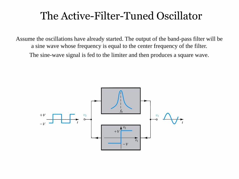
The Active-Filter-Tuned Oscillator
Assume the oscillations have already started. The output of the band-pass filter will be
a sine wave whose frequency is equal to the center frequency of the filter.
The sine-wave signal is fed to the limiter and then produces a square wave.

Practical implementation of the active-filter-tuned oscillator
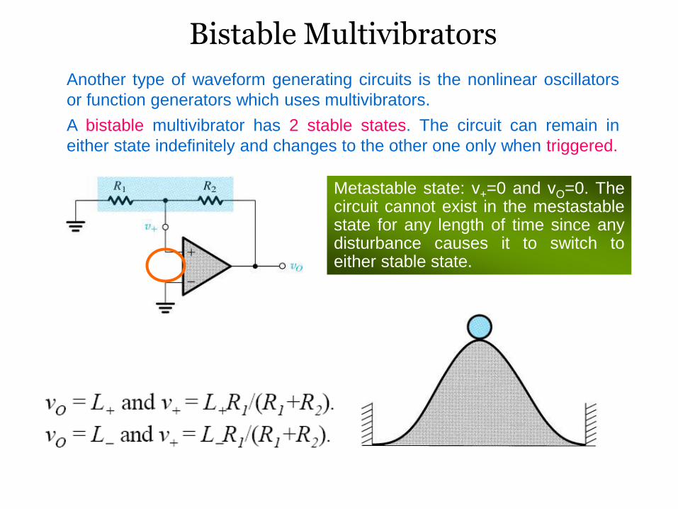
Bistable Multivibrators
Another type of waveform generating circuits is the nonlinear oscillators
or function generators which uses multivibrators.
A bistable multivibrator has 2 stable states. The circuit can remain in
either state indefinitely and changes to the other one only when triggered.
Metastable state: v+=0 and vO=0. The circuit cannot exist in the mestastable state for any length of time since any disturbance causes it to switch to either stable state.
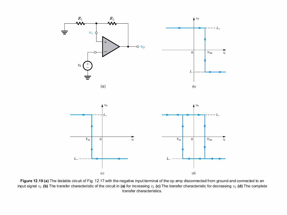

Bistable Circuit with Inverting Transfer Characteristics
Assume that vO is at one of its two possible levels, say L+, and thus v+ = βL+.
As vI increases from 0 and then exceeds βL+, a negative voltage developes between
input terminals of the op amp.
This voltage is amplified and vO goes negative.
The voltage divider causes v+ to go negative, increasing the net negative input and
keeping the regenerative process going.
This process culminates in the op amp saturating, that is, vO = L-.
The circuit is said to be inverting Trigger signal
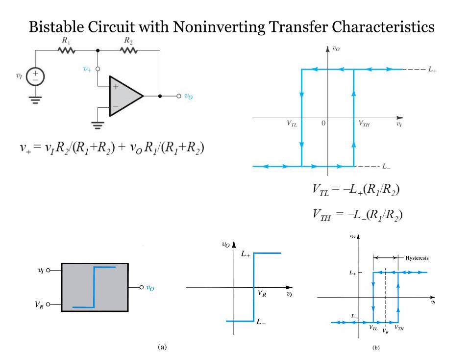
Bistable Circuit with Noninverting Transfer Characteristics

Application of the Bistable Circuit as a Comparator
To design a circuit that detects and counts the zero crossings of an arbitrary
waveform, a comparator whose threshold is set to 0 can be used. The comparator
provides a step change at its output every time zero crossing occurs.
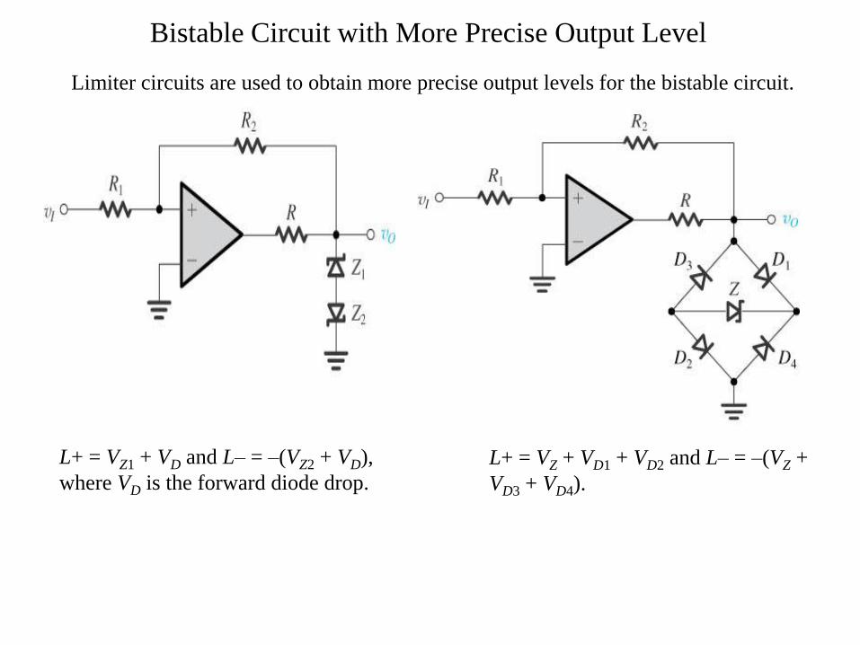
Bistable Circuit with More Precise Output Level
Limiter circuits are used to obtain more precise output levels for the bistable circuit.
L+ = VZ + VD1 + VD2 and L– = –(VZ +
VD3 + VD4).
L+ = VZ1 + VD and L– = –(VZ2 + VD),
where VD is the forward diode drop.
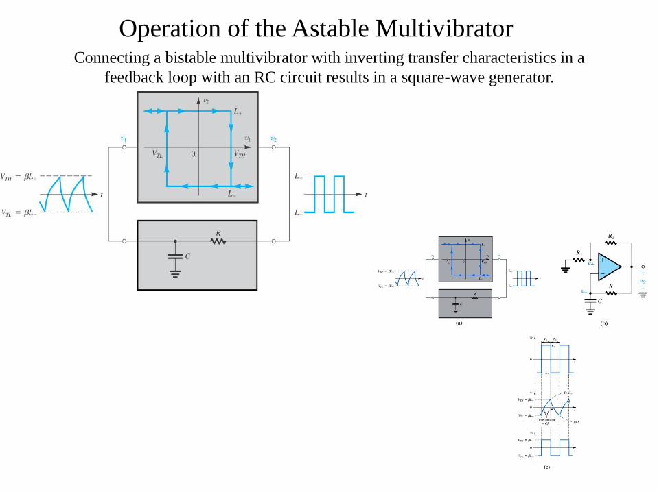
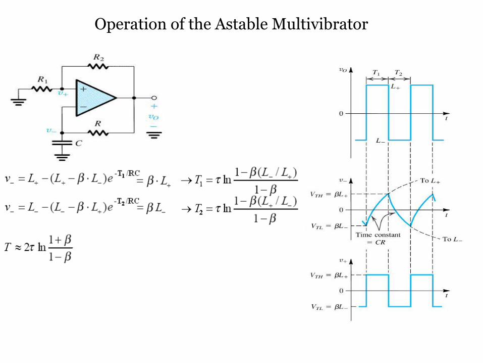
Operation of the Astable Multivibrator Connecting a bistable multivibrator with inverting transfer characteristics in a
feedback loop with an RC circuit results in a square-wave generator.
Operation of the Astable Multivibrator
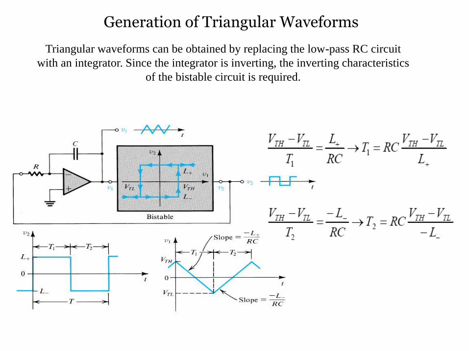
Generation of Triangular Waveforms
Triangular waveforms can be obtained by replacing the low-pass RC circuit
with an integrator. Since the integrator is inverting, the inverting characteristics
of the bistable circuit is required.
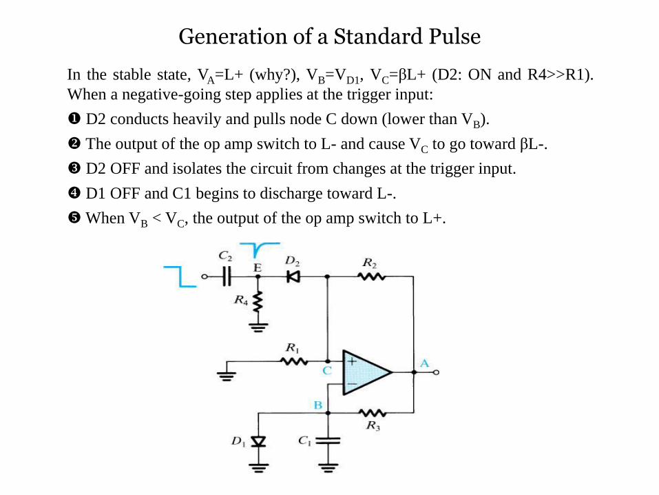
Generation of a Standard Pulse
In the stable state, VA=L+ (why?), VB=VD1, VC=βL+ (D2: ON and R4>>R1).
When a negative-going step applies at the trigger input:
D2 conducts heavily and pulls node C down (lower than VB).
The output of the op amp switch to L- and cause VC to go toward βL-.
D2 OFF and isolates the circuit from changes at the trigger input.
D1 OFF and C1 begins to discharge toward L-.
When VB < VC, the output of the op amp switch to L+.

Generation of a Standard Pulse

The 555 Circuit
Commercially available integrated-circuit package such as 555 timer exists that
contain the bulk of the circuitry needed to implement monostable and astable
multivibrator.
2/3 VCC
1/3 VCC