Embed Size (px)
Citation preview
Portable GPS Baseband Logging
Morgan Quigley, Stanford UniversityPieter Abbeel, Stanford University
Dave De Lorenzo, Stanford UniversityYi Gu, Stanford University
Sara Bolouki, Stanford UniversityDennis Akos, University of ColoradoAndrew Y. Ng, Stanford University
BIOGRAPHY
Morgan Quigley and Pieter Abbeel are Ph.D. candidates inthe Computer Science Department at Stanford University.
Yi Gu is a Ph.D. candidate in the Electrical EngineeringDepartment at Stanford University.
Sara Bolouki is a graduate student in the Electrical Engi-neering Department at Stanford University.
Dr. Dave S. De Lorenzo is a Research Associate in the GPSLaboratory at Stanford University, where he is studyingspace-time adaptive antenna array processing and GNSSsoftware receivers.
Dr. Andrew Y. Ng is an Assistant Professor in the Com-puter Science Department at Stanford University. His re-search interests include machine learning, robotic percep-tion and control, and broad-competence artificial intelli-gence.
Dr. Dennis Akos is an Assistant Professor in the AerospaceEngineering Science Department at the University of Col-orado at Boulder.
ABSTRACT
We present the design and implementation of a highlyportable multi-antenna datalogging system which can logseveral minutes of multi-channel raw GPS L1 baseband.In addition, our design interleaves two serial data streamswith the baseband data, allowing, e.g., inertial data to re-main synchronized with the data stream. The system isFPGA-based and uses two CompactFlash cards for stor-age. The data is extracted by imaging the CompactFlashcards onto a PC and recovering synchronization codes in-terleaved with the baseband data. The resulting system isuseful for multi- (and single-) antenna receiver develop-ment, as it allows for simple data collection. The data files
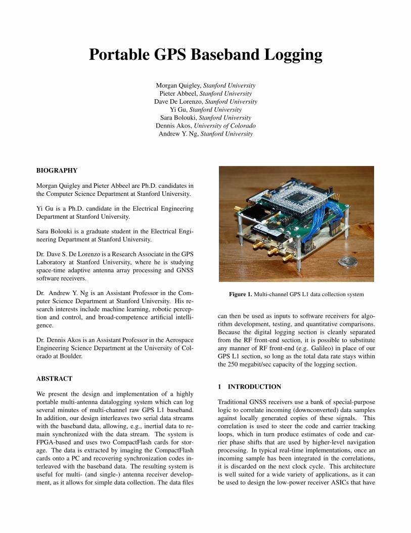
Figure 1. Multi-channel GPS L1 data collection system
can then be used as inputs to software receivers for algo-rithm development, testing, and quantitative comparisons.Because the digital logging section is cleanly separatedfrom the RF front-end section, it is possible to substituteany manner of RF front-end (e.g. Galileo) in place of ourGPS L1 section, so long as the total data rate stays withinthe 250 megabit/sec capacity of the logging section.
1 INTRODUCTION
Traditional GNSS receivers use a bank of special-purposelogic to correlate incoming (downconverted) data samplesagainst locally generated copies of these signals. Thiscorrelation is used to steer the code and carrier trackingloops, which in turn produce estimates of code and car-rier phase shifts that are used by higher-level navigationprocessing. In typical real-time implementations, once anincoming sample has been integrated in the correlations,it is discarded on the next clock cycle. This architectureis well suited for a wide variety of applications, as it canbe used to design the low-power receiver ASICs that have
contributed to the dramatic drop in GPS receiver prices inrecent years. However, this architecture does not lend itselfwell to receiver design and signal analysis, as the raw RFbaseband is not available for experimentation.
In this paper, we describe the design and implementation ofa portable device, shown in Figure 1, which is well suitedto receiver research and algorithm development. This de-vice captures every data sample from a 6-antenna array andsaves it to a flash-based storage. The saved samples can belater converted to PC files for receiver algorithm develop-ment on real-world data.
1.1 Motivation
In the Stanford Computer Science Department, ongoing re-search has produced advances in the state of the art of aer-obatic autonomous helicopter flight [1]. In prior work, wehave presented applications of statistical machine learningtechniques to aerobatic R/C helicopter system identifica-tion (model building) and controller generation. We haveused these techniques to successfully derive controllers ca-pable of autonomous inverted hovering, rolls, flips, funnels,and a variety of other maneuvers.
However, as we have continued to push our airframes andalgorithms into ever more agressive maneuvers, we havefound that obtaining accurate (centimeter-level) localiza-tion is rather difficult. This is particularly true in aero-batic maneuvers that require the helicopter to repeatedlytransition through inverted orientations. In our experience,single-antenna GPS receivers, even very good ones, can-not rapidly re-acquire carrier lock in such situations. Asa consequence, state estimation would have to rely solelyon inertial integration, which in our experiments is MEMS-based and thus state estimation degrades rapidly.
Therefore, we have begun to investigate the feasibility ofconstructing a multi-antenna GPS receiver which providesomnidirectional reception via antenna switching. As a firststep in this undertaking, we describe the construction of amulti-antenna datalogging device which is capable of op-erating onboard our helicopter platform and collecting theraw GPS baseband streams emitted by a collection of RFfront-end chips.
1.2 Application areas
A portable, robust, easy-to-operate baseband data collec-tion system is of great utility in designing GPS receiveralgorithms. By capturing the raw output of RF front-endchips, multi-antenna receiver algorithm development canhappen offline in software. The datalogging device is par-ticularly useful if experiments, such as helicopter flights,have practical difficulties or are challenging to simulate.
Other applications, such as bistatic radar, could also ben-efit from offline processing of data.
High-fidelity single-antenna simulators have existed fora number of years in the GNSS community. However,obtaining real-world multi-antenna data helps increase thelikelihood that receiver algorithms designed in softwarewill work in a wide variety of real-world situations, assome multi-antenna experiments can be difficult to model.
2 ENVIRONMENTAL CONSTRAINTS
The R/C helicopter application imposed numerous restric-tions on our design. Because these restrictions were thedeciding factor in several design choices, we will providesome details of the R/C helicopter environment.
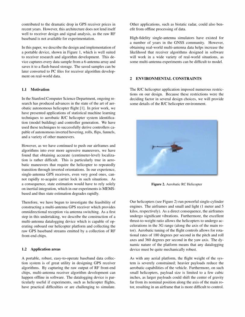
Figure 2. Aerobatic RC Helicopter
Our helicopters (see Figure 2) run powerful single-cylinderengines. The airframes and small and light (1 meter and 5kilos, respectively). As a direct consequence, the airframesundergo significant vibrations. Furthermore, the excellentthrust-to-weight ratio allows the helicopters to undergo ac-celerations in the 3G range (along the axis of the main ro-tor). Aerobatic tuning of the flight controls allows for rota-tional rates of 180 degrees per second in the pitch and rollaxes and 360 degrees per second in the yaw axis. The dy-namic nature of the platform means that any dataloggingdevice must be quite mechanically robust.
As with any aerial platform, the flight weight of the sys-tem is severely constrained; heavier payloads reduce theaerobatic capabilities of the vehicle. Furthermore, on suchsmall helicopters, payload size is limited to a few cubicinches, as larger payloads could shift the center of gravityfar from its nominal position along the axis of the main ro-tor, resulting in an airframe that is more difficult to control.
3 DATA STORAGE
There are several options for storing the baseband data. Thefollowing sections describe the various options and theirrespective feasability for the R/C helicopter application.
3.1 DRAM
A large DRAM module could serve as a data store: thehardware could fill the DRAM with the sample data, andlater dump this data to a PC for permanent storage. Thisoption has the advantage of being relatively simple, but itis limited by the size of DRAM modules that are readilyobtainable (at time of writing, modules larger than 4 GBare rather expensive). Furthermore, a loss of power beforethe DRAM module has been copied out of the dataloggerwill result in the loss of all data.
3.2 Mechanical hard drive
Mechanical hard drives have been successfully used in thepast [2], [3] to create multi-antenna dataloggers. Becauselaptop hard drives are readily obtainable, this solutionwould be inexpensive and have a very large capacity. How-ever, we chose not to pursue this concept due to the severevibrations and accelerations our platform experiences innormal operation. Because the vibration of our platformis approximately double the vibration rating of most con-sumer hard drives, we feared that head crashes woulddestroy a hard drive-based datalogger.
3.3 Solid-state hard drives
Solid state hard drives are gaining momentum in the com-puter industry as replacements for mechanical hard drives.These drives can use the same ATAPI protocol and formfactor as mechanical drives, but they implement data stor-age using flash memory instead of rotating platters. Al-though these drives are dropping in price, a large solid-statedrive with high throughput costs several thousand dollarsat time of writing. This option was not pursued simply be-cause of cost; as prices continue to fall, solid-state drivesmay become a viable option for portable datalogging.
3.4 USB flash drive
USB flash drives have previously been used to record dual-antenna data [4]. In that work, the logging system was asmall form factor (nano-ITX) PC with two USB flash drivesfor storage. The resultant system was small enough to flyon a balloon for successful experiments. However, as wewere seeking to reduce weight and power even further inour logger design, we chose not to follow the embedded
PC approach in this work, opting instead for a fully FPGA-based system. Since we did not have a host PC, USB flashdrives were not an option in our design.
3.5 Removable Flash Media
There are a variety of removable flash media formats cur-rently used in mass-market digital cameras. Flash cards ofeach of these formats are readily obtainable. However, ac-cess to the technical specifications of many formats requiresignificant licensing fees.
For this project, we chose to use the CompactFlash stan-dard. Its specification is freely available, and the fastestCompactFlash cards currently provide the highest sus-tained throughput among the various removable flash stan-dards.
CompactFlash cards can run in several operational modes.We chose the “True IDE” mode, which means the card isoperated by the parallel ATA (PATA) protocol. Various ver-sions of this protocol have been in use for decades. Thus,documentation and open-source software and hardware im-plementations are widely available.
4 WRITE STALLS
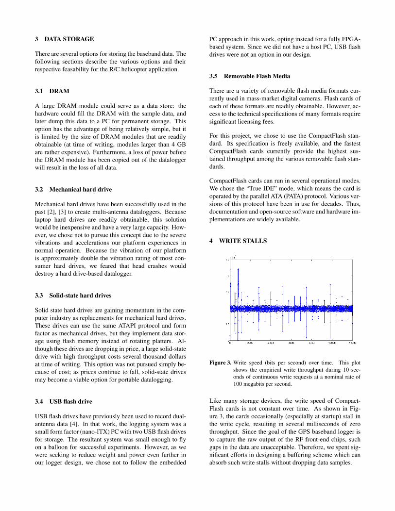
Figure 3. Write speed (bits per second) over time. This plotshows the empirical write throughput during 10 sec-onds of continuous write requests at a nominal rate of100 megabits per second.
Like many storage devices, the write speed of Compact-Flash cards is not constant over time. As shown in Fig-ure 3, the cards occasionally (especially at startup) stall inthe write cycle, resulting in several milliseconds of zerothroughput. Since the goal of the GPS baseband logger isto capture the raw output of the RF front-end chips, suchgaps in the data are unacceptable. Therefore, we spent sig-nificant efforts in designing a buffering scheme which canabsorb such write stalls without dropping data samples.
5 FRONT-END BOARD
Our front-end board is based around the SiGe SE4110L.The RF signal from a GPS L1 antenna is fed into the chip,which then outputs a downconverted and digitized versionas a 2-bit digital stream at 16.368 MHz.
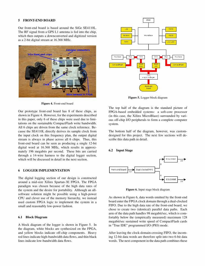
Figure 4. Front-end board
Our prototype front-end board has 8 of these chips, asshown in Figure 4. However, for the experiments describedin this paper, only 6 of these chips were used due to limi-tations on the sustainable CompactFlash write bandwidth.All 6 chips are driven from the same clock reference. Be-cause the SE4110L directly derives its sample clock fromthe input clock on this frequency plan, the output digitalstream is always in phase across all 6 chips. Thus, thisfront-end board can be seen as producing a single 12-bitdigital word at 16.368 MHz, which results in approxi-mately 196 megabits per second. These bits are carriedthrough a 14-wire harness to the digital logger section,which will be discussed in detail in the next section.
6 LOGGER IMPLEMENTATION
The digital logging section of our design is constructedaround a mid-size Xilinx Spartan-3E FPGA. The FPGAparadigm was chosen because of the high data rates ofthe system and the desire for portability. Although an all-software solution might be possible using a high-powerCPU and clever use of the memory hierarchy, we insteadused custom FPGA logic to implement the system in asmall and reasonably low-power fashion.
6.1 Block Diagram
A block diagram of the logger is shown in Figure 5. Inthe diagram, white blocks are synthesized on the FPGA,and yellow blocks indicate off-chip components. Heavyred lines indicate high-bandwidth data flows, and thin blacklines indicate low-bandwidth data flows.
Figure 5. Logger block diagram
The top half of the diagram is the standard picture ofFPGA-based embedded systems: a soft-core processor(in this case, the Xilinx MicroBlaze) surrounded by vari-ous off-chip I/O peripherals to form a complete computersystem.
The bottom half of the diagram, however, was custom-designed for this project. The next few sections will de-scribe this data path in detail.
6.2 Input Stage
Figure 6. Input stage block diagram
As shown in Figure 6, data words emitted by the front-endboard enter the FPGA clock domain through a dual-clockedFIFO. Due to the high data rate of the front-end board, wechose to create two (identical) parallel data paths. Eacharm of the data path handles 98 megabit/sec, which is com-fortably below the (empirically measured) maximum 128megabit/sec sustained write speed of CompactFlash cardsin “True IDE” programmed I/O (PIO) mode.
After leaving the clock-domain-crossing FIFO, the incom-ing 12-bit data words are therefore split into two 6-bit datawords. The next component in the data path combines these
6-bit data words to form a stream of 16-bit data words.Since the least common multiple of 6 and 16 is 48, theconversion is performed by an 8-state logic block whichproduces three 16-bit data words for every eight 6-bit in-puts.
6.3 Input FIFO, Mux, and Synchronization Codes
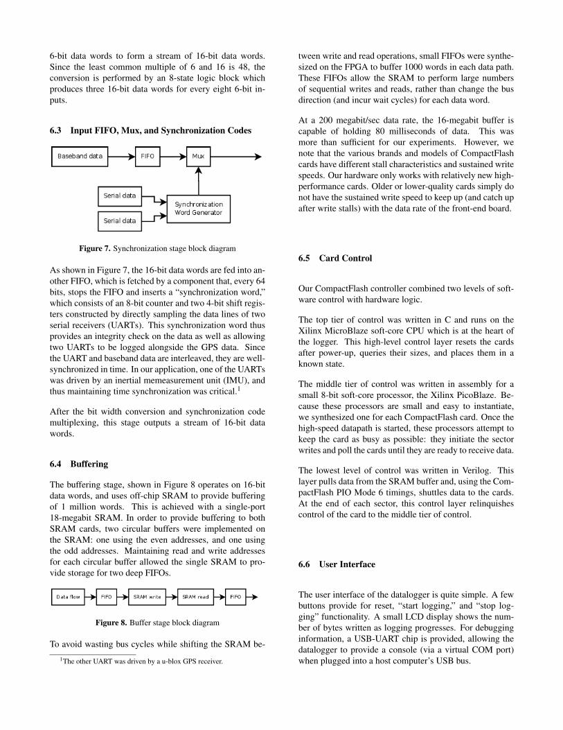
Figure 7. Synchronization stage block diagram
As shown in Figure 7, the 16-bit data words are fed into an-other FIFO, which is fetched by a component that, every 64bits, stops the FIFO and inserts a “synchronization word,”which consists of an 8-bit counter and two 4-bit shift regis-ters constructed by directly sampling the data lines of twoserial receivers (UARTs). This synchronization word thusprovides an integrity check on the data as well as allowingtwo UARTs to be logged alongside the GPS data. Sincethe UART and baseband data are interleaved, they are well-synchronized in time. In our application, one of the UARTswas driven by an inertial memeasurement unit (IMU), andthus maintaining time synchronization was critical.1
After the bit width conversion and synchronization codemultiplexing, this stage outputs a stream of 16-bit datawords.
6.4 Buffering
The buffering stage, shown in Figure 8 operates on 16-bitdata words, and uses off-chip SRAM to provide bufferingof 1 million words. This is achieved with a single-port18-megabit SRAM. In order to provide buffering to bothSRAM cards, two circular buffers were implemented onthe SRAM: one using the even addresses, and one usingthe odd addresses. Maintaining read and write addressesfor each circular buffer allowed the single SRAM to pro-vide storage for two deep FIFOs.
Figure 8. Buffer stage block diagram
To avoid wasting bus cycles while shifting the SRAM be-
1The other UART was driven by a u-blox GPS receiver.
tween write and read operations, small FIFOs were synthe-sized on the FPGA to buffer 1000 words in each data path.These FIFOs allow the SRAM to perform large numbersof sequential writes and reads, rather than change the busdirection (and incur wait cycles) for each data word.
At a 200 megabit/sec data rate, the 16-megabit buffer iscapable of holding 80 milliseconds of data. This wasmore than sufficient for our experiments. However, wenote that the various brands and models of CompactFlashcards have different stall characteristics and sustained writespeeds. Our hardware only works with relatively new high-performance cards. Older or lower-quality cards simply donot have the sustained write speed to keep up (and catch upafter write stalls) with the data rate of the front-end board.
6.5 Card Control
Our CompactFlash controller combined two levels of soft-ware control with hardware logic.
The top tier of control was written in C and runs on theXilinx MicroBlaze soft-core CPU which is at the heart ofthe logger. This high-level control layer resets the cardsafter power-up, queries their sizes, and places them in aknown state.
The middle tier of control was written in assembly for asmall 8-bit soft-core processor, the Xilinx PicoBlaze. Be-cause these processors are small and easy to instantiate,we synthesized one for each CompactFlash card. Once thehigh-speed datapath is started, these processors attempt tokeep the card as busy as possible: they initiate the sectorwrites and poll the cards until they are ready to receive data.
The lowest level of control was written in Verilog. Thislayer pulls data from the SRAM buffer and, using the Com-pactFlash PIO Mode 6 timings, shuttles data to the cards.At the end of each sector, this control layer relinquishescontrol of the card to the middle tier of control.
6.6 User Interface
The user interface of the datalogger is quite simple. A fewbuttons provide for reset, “start logging,” and “stop log-ging” functionality. A small LCD display shows the num-ber of bytes written as logging progresses. For debugginginformation, a USB-UART chip is provided, allowing thedatalogger to provide a console (via a virtual COM port)when plugged into a host computer’s USB bus.
6.7 Runtime
Using two 8-gigabyte flash cards, the system can store ap-proximately 10 minutes of data using the front-end boarddescribed previously, which emits data at a rate of 200megabit/sec. Naturally, this recording time would doubleif 16-gigabyte flash cards were used, and even higher carddensities will likely emerge in the future.
A simple 3.3-volt switching power supply was imple-mented, allowing the datalogger to be directly driven fromany DC power source in the 5-15 volt range. For ourexperiments, we powered the system from 3-cell lithium-polymer batteries. The nominal power draw of the systemwas 2 watts. The optional LCD backlight drew another 1watt when powered on. This means that a 3-cell lithium-polymer battery will power the system for approximatelytwo hours, although this runtime is somewhat irrelevantbecause the logging capacity of the data store is an orderof magnitude less.
6.8 Physical Layout
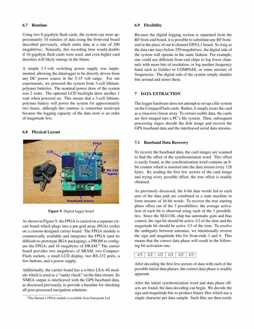
Figure 9. Digital logger board
As shown in Figure 9, the FPGA is carried on a separate cir-cuit board which plugs into a pin-grid array (PGA) socketon a custom-designed carrier board. The FPGA module iscommercially available and integrates the FPGA (and itsdifficult-to-prototype BGA packaging), a PROM to config-ure the FPGA, and 16 megabytes of DRAM.2 The carrierboard provides two megabytes of SRAM, two Compact-Flash sockets, a small LCD display, two RS-232 ports, afew buttons, and a power supply.
Additionally, the carrier board has a u-blox LEA-4S mod-ule which is used as a “sanity check” on the data stream. ItsNMEA output is interleaved with the GPS baseband data,as discussed previously, to provide a baseline for checkingall post-processed navigation solutions.
2The Darnaw1 FPGA module is available from Enterpoint Ltd.
6.9 Flexibility
Because the digital logging section is separated from theRF front-end board, it is possible to substitute any RF front-end in the place of our 6-channel GPS L1 board. So long asthe data rate stays below 250 megabit/sec, the digital side ofthe system will operate in the same fashion. For example,one could use different front-end chips to log fewer chan-nels with more bits of resolution, or log another frequencyband such as Galileo or COMPASS, or some mixture offrequencies. The digital side of the system simply shuttlesbits around and stores them.
7 DATA EXTRACTION
The logger hardware does not attempt to set up a file systemon the CompactFlash cards. Rather, it simply treats the cardas a (massive) linear array. To extract usable data, the cardsare first imaged into a PC’s file system. Then, subsequentprocessing stages decode the disk image and recover theGPS baseband data and the interleaved serial data streams.
7.1 Baseband Data Recovery
To recover the baseband data, the card images are scannedto find the offset of the synchronization word. This offsetis easily found, as the synchronization word contains an 8-bit counter which is inserted into the data stream every 128bytes. By reading the first few sectors of the card imageand trying every possible offset, the true offset is readilyobtained.
As previously discussed, the 6-bit data words fed to eacharm of the data path are combined in a state machine toform streams of 16-bit words. To recover the true startingphase offset out of the 3 possibilities, the average activa-tion of each bit is observed using each of the 3 possibili-ties. Since the SE4110L chip has automatic gain and biascontrol, the sign bit should be active 1/2 of the time and themagnitude bit should be active 1/3 of the time. To resolvethe ambiguity between antennas, we intentionally reversethe sign and magnitude bits for front-ends 1 and 4. Thismeans that the correct data phase will result in the follow-ing bit activation rate:
1/3 1/2 1/2 1/3 1/2 1/3
After decoding the first few sectors of data with each of thepossible initial data phases, the correct data phase is readilyapparant.
After the initial synchronization word and data phase off-sets are found, the data decoding can begin. We decode thesign and magnitude bits to produce binary files which use asingle character per data sample. Such files are then easily
imported into MATLAB or read by other languages.
7.2 Serial data recovery
To recover the two serial streams, their shift registers arefirst extracted from the synchronization words. Then, insoftware, we perform exactly what a UART does in hard-ware: wait for the start bit, then (using the previouslyknown baud rate) sample the data bits, and finally ensurethat a valid stop bit is present. Our software then writesthis data stream to a binary file for further processing.
In our experiments, one serial stream was the ASCIINMEA data from a GPS receiver module, and the otherstream was 300-Hertz inertial data (3-axis accelerome-ters, angular rate sensors, and magnetometers). While theNMEA data could be read directly with a text editor, theinertial data required another decoding stage to produce atext file suitable for importing into MATLAB.
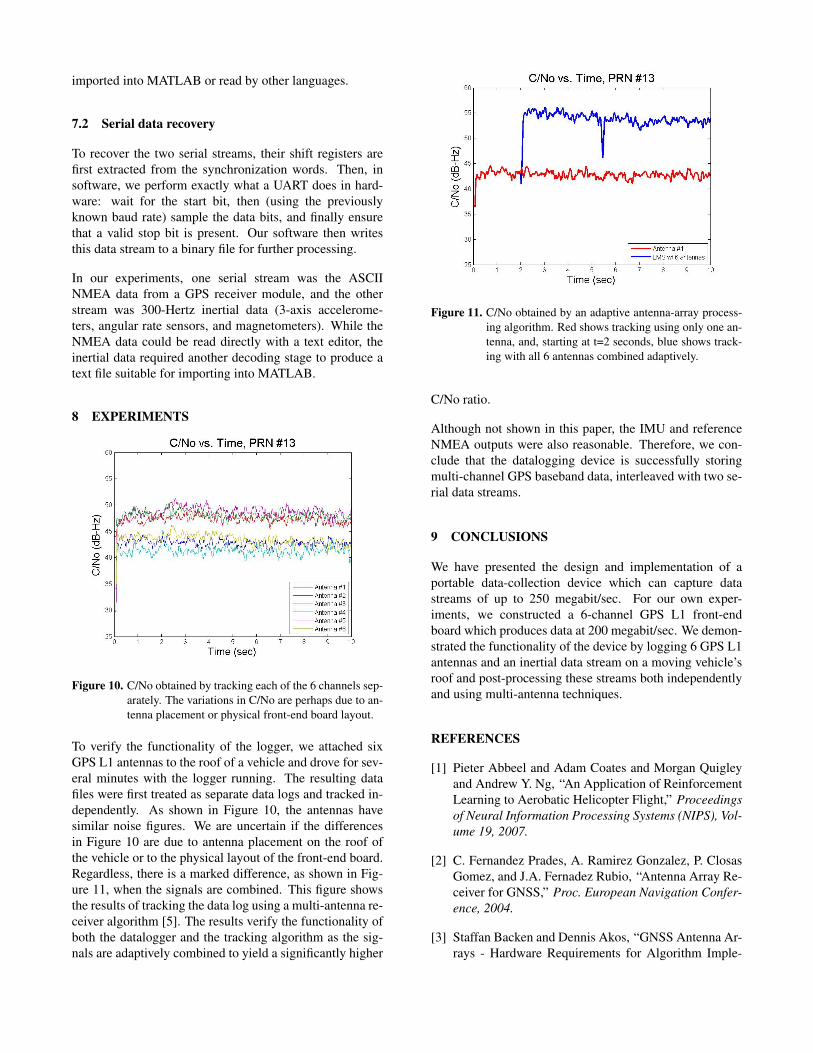
8 EXPERIMENTS
Figure 10. C/No obtained by tracking each of the 6 channels sep-arately. The variations in C/No are perhaps due to an-tenna placement or physical front-end board layout.
To verify the functionality of the logger, we attached sixGPS L1 antennas to the roof of a vehicle and drove for sev-eral minutes with the logger running. The resulting datafiles were first treated as separate data logs and tracked in-dependently. As shown in Figure 10, the antennas havesimilar noise figures. We are uncertain if the differencesin Figure 10 are due to antenna placement on the roof ofthe vehicle or to the physical layout of the front-end board.Regardless, there is a marked difference, as shown in Fig-ure 11, when the signals are combined. This figure showsthe results of tracking the data log using a multi-antenna re-ceiver algorithm [5]. The results verify the functionality ofboth the datalogger and the tracking algorithm as the sig-nals are adaptively combined to yield a significantly higher
Figure 11. C/No obtained by an adaptive antenna-array process-ing algorithm. Red shows tracking using only one an-tenna, and, starting at t=2 seconds, blue shows track-ing with all 6 antennas combined adaptively.
C/No ratio.
Although not shown in this paper, the IMU and referenceNMEA outputs were also reasonable. Therefore, we con-clude that the datalogging device is successfully storingmulti-channel GPS baseband data, interleaved with two se-rial data streams.
9 CONCLUSIONS
We have presented the design and implementation of aportable data-collection device which can capture datastreams of up to 250 megabit/sec. For our own exper-iments, we constructed a 6-channel GPS L1 front-endboard which produces data at 200 megabit/sec. We demon-strated the functionality of the device by logging 6 GPS L1antennas and an inertial data stream on a moving vehicle’sroof and post-processing these streams both independentlyand using multi-antenna techniques.
REFERENCES
[1] Pieter Abbeel and Adam Coates and Morgan Quigleyand Andrew Y. Ng, “An Application of ReinforcementLearning to Aerobatic Helicopter Flight,” Proceedingsof Neural Information Processing Systems (NIPS), Vol-ume 19, 2007.
[2] C. Fernandez Prades, A. Ramirez Gonzalez, P. ClosasGomez, and J.A. Fernadez Rubio, “Antenna Array Re-ceiver for GNSS,” Proc. European Navigation Confer-ence, 2004.
[3] Staffan Backen and Dennis Akos, “GNSS Antenna Ar-rays - Hardware Requirements for Algorithm Imple-
mentation,” Royal Institute of Navigation EuropeanNavigation Conference & Exhibition (ENC), Manch-ester, UK, May 2006.
[4] Stephan Esterhuizen and Dennis Akos, “The Design,Construction, and Testing of a Modular GPS BistaticRadar Software Receiver for Small Platforms,” GNSSR’06: Workshop on GNSS Reflections, ESTEC, Noord-wijk, Netherlands, June 2006.
[5] David S. De Lorenzo, “Navigation Accuracy and Inter-ference Rejection for GPS Adaptive Antenna Arrays,”PhD Thesis, Department of Aeronautics and Astronau-tics, Stanford University, 2007.