Embed Size (px)
Citation preview

Polybook - Solid State Physics and Chemistry of Materials: 1
Polybook - Solid State Physics and Chemistry of Materials: 1
Nicola Spaldin, Christoph Murer, Cristina Mercandetti, and with contributions from the 2017 students
Sara Morgenthaler
Polybook - Solid State Physics and Chemistry of Materials: 1 Copyright © by Nicola Spaldin, Christoph Mur-er, Cristina Mercandetti, and with contributions from the 2017 students. All Rights Reserved.

Contents Class Goals and Philosophy 3
I. Electrical and Thermal Properties of Metals Introduction 1. 6 Properties of metals within classical mechanics 2. 7 Properties of metals within quantum mechanical free-electron theory 3. 12 A little bit more quantum mechanics -- operators and measurements 4. 25 Summary 5. 32
II. Solving the Schrödinger equation for an atom Introduction 6. 34 Particle on a ring 7. 35 Particle on a sphere 8. 39 Particle in a coulombic 1/r potential 9. 41 How do the quantum numbers correspond to the familiar atomic orbitals? 10. 43 The Schrödinger equation for the H₂ molecule 11. 45 Summary 12. 48
III. Linear combination of atomic orbitals (LCAO) Molecular orbitals from LCAOs 13. 50 Formal statement and proof of the variational principle 14. 53 Application of the variational principle to the H₂ molecule 15. 54 Other covalent diatomic molecules 16. 56 Heteronuclear diatomics and polar bonds (e.g. HF) 17. 58 Summary 18. 59 LCAO theory for solids 19. 60
IV. Using bandstructures to understand and explain the properties of solids Properties of metals from the band structure 20. 70 Semiconductor properties and bandstructures 21. 74 Band structures of some insulating materials 22. 84 Coupling with structure 23. 91 Summary 24. 97
V. Magnetism The magnetic moment of an electron 25. 100 Magnetic moments in atoms 26. 103 Ferromagnetism in transition metals 27. 107 Magnetoresistance 28. 109 Antiferromagnetism in transition metals 29. 115 Magnetism in Transition Metal Oxides 30. 118 How is AFM Ordering measured? 31. 127 Summary 32. 129
Appendix 130

Class Goals and Philosophy
The goal of this class is to understand the relationship between the properties of materials and their underlying chemistry and structure. So if we are given a particular type and arrangement of atoms, we will be able to work out and understand what the properties will be, and converse-ly, if we want a material with specific properties, we will know which atoms to choose and how to arrange them.
We know of course that the behavior of electrons in solids is described well by the quantum mechanical Schrödinger equation (or in some cases its relativistic extension, the Dirac equa-tion) and in principle all properties of known atomic arrangements can be calculated from its solution. In practice, however, solution of the Schrödinger equation is intractable for all but the simplest cases, and we have to use approximations. Indeed, understanding when and where particular approximations work or fail also gives us important insights into the underly-ing physics that dominate the behavior.
In fact we will start the course by investigating how far classical physics can take us in describing the behavior of electrons. We will see that for some properties of simple metals, a classical picture in which the electrons follow Newton’s laws and the classical electrostatic equations gives a good description. This is intriguing as the approximations are so egregious, and we will discuss later in the course how “hidden” quantum mechanics contributes to the classical description’s success. We will then move on to see how much further treating the electrons quantum mechanically, but neglecting their interactions with each other and with external potentials such as the ions in a lattice, takes us. Again we will have some successes in spite of the still rather shocking assumptions, but we will also still have some glaring failures in comparing theoretical predictions with experimental observations.
Perhaps surprisingly, many of these problems will be fixed at the next level of complexity in approximation, in which we assume that the electrons interact with the lattice but still do not interact explicitly with each other. This “single-particle approximation” is the level of quan-tum mechanics that most of us become familiar with in our introductory quantum mechanics classes: First we solve the following Schrödinger equation for one electron interacting with an external potential:
This gives us the corresponding energy levels and wave functions for a single electron. Then if we have more than one electron in our real system, we fill up the energy levels starting with the lowest energy and we acknowledge the Pauli principle by putting only two electrons (of opposite spin) in each level. But we kind of brush over the fact that the electrons should then have a Coulomb interaction with each other. Remarkably, this works very well in many cases, and a wide range of properties of a wide range of materials can be rather accurately modeled and understood at this level. Often we rewrite the Schrödinger equation in the form:
So we see that the Schrödinger equation is an eigenvalue equation, and that the single-par-ticle wavefunctions are eigenfunctions of the energy operator, , which we call the Hamilton-ian.
There are of course many examples of materials and properties — transition metal oxides that show exotic superconductivity, or metal-insulator transitions are prototypical — in which the electrons interact strongly with each other and can not be treated within a single-particle approximation. We call such materials strongly correlated because the behavior of any electron directly affects all the other electrons in the system. To describe them properly we should really solve the many-body Schrödinger equation below, which includes the Coulomb interactions explicitly.
Here the sum is over all the electrons in the system, , and is a many-body wave-function that depends explicitly on the coordinates of all the electrons, . In practice the full many-body Schrödinger equation is intractable for all but the simplest of systems so we will explore approximations that can capture important aspects of the many-body behavior. We’ll see that, while these approximations can in some cases give us some amount of predictive capability, many aspects of the physics of strongly correlated materials remain exotic and mys-terious and are an exciting frontier for ongoing research.

But first let’s begin with the properties of simple metals.

I
Electrical and Thermal Properties of Metals

1
Introduction
Let’s start by considering the phenomena of electrical conductivity and its reciprocal, electrical resistivity. While these are not at first sight the most glamorous material properties, they are remarkable in that they vary over a huge range even in simple materials — diamond for exam-ple has a resistivity of ohm-m, whereas that of copper is ohm-m. They are also of tremendous technological importance. Much of the information technology industry rests on the transfer of electrons from one place to another, and of course the transmission of energy throughout the power grid is achieved through the flow of electrical current. Typical transmission line wires have losses to resistive heating of around 5% which is estimated to cost tens of billions of dollars per year in the United States alone. We see then that the thermal properties of metals are also tremendously important so we will discuss those here too.

2
Properties of metals within classical mechanics
We will begin by exploring how far we can describe the properties of metals using the simplest possible classical theory, in which the electrons are classical particles that don’t interact with each other — we call such electrons free electrons.
2.1 – Ohm’s Law One of the most well-known features of many metals is that they obey Ohm’s law, which describes metallic conduction in the case when the resistance is independent of the applied voltage. This so-called ohmic behavior is common in many metals and semiconductors over a wide range of voltages. Usually Ohm’s law is expressed as
Where is the voltage, the current, the electric field and the current density. We will find it convenient to work with the following form of Ohm’s law, which is easily
obtained from the conventional definition by rearranging using the usual definitions of electri-cal quantities summarized in the following section:
Definition: Resistivity
where is the resistivity, the resistance, the cross-sectional area and the length.
Definition: Conductivity
where is the conductivity and is the resistivity.
Definition: Electric field
where is the electric field, the voltage and the length.
Definition: Current density
where is the current density, the current and the cross-sectional area.
2.2 – The Drude Model – Classical Free Electrons So let’s see whether classical mechanics with non-interacting electrons predicts ohmic behav-ior. The assumptions that go into the model that we will use, which is often called the Drude model after its originator are:
a. The electrons are classical particles, separated from their parent ions and able to wander around in the solid. This is our usual classical picture of metallic bonding.
b. The electrons do not interact with each other either through their charges or through collisions, and their only interaction with the positively charged ions is to collide with them and bounce off again. So all Coulomb interactions are neglected. Such electrons are called “free electrons”.
Since the electrons are classical particles, their thermal behavior is described by classical ther-
modynamics, which tells us that they have an average kinetic energy per
degree of freedom in three dimensions. This means that the velocity that the elec-
trons have as a result of their temperature, which we call their thermal velocity, is
This is approximately m/s at 300 K. The thermal velocity does not contribute to the electrical current as it does not have a pre-
ferred direction. When an electric field is applied, however, the electrons achieve an aver-age drift velocity in the direction opposite to the field. The corresponding current density from the electron drift is
where is the number of free electrons per unit volume and is the magnitude of the electronic charge, C. Remember that Ohm’s law is fulfilled if with independent of , which we see corresponds in turn to a drift velocity that is linearly propor-tional to the applied field, .
So let’s now derive an expression for the drift velocity in terms of microscopic properties, and see if it’s really linearly proportional to . If so, the simple classical model will have correctly reproduced Ohm’s law behavior!
Combining Newton’s second law and basic electrostatics gives us the acceleration of the electron, :
with the mass of the electron. We see that an electron in vacuum would have a constant acceleration and a steadily increas-
ing velocity! In fact the electrons collide with ions and are slowed down as they transfer their kinetic energy to the lattice. We call the average time between collosions, , the collision or relaxation time. Then the average drift velocity is just this time multiplied by the acceleration:
Substituting the expression for the acceleration, , in the equation above for the average drift velocity gives
and Ohm’s law is satisfied if , and are independent of . Clearly this applies for and , which are fundamental constants. What about the time between collisions? Well, in the limit that , the rate at which the electron undergoes collisions is determined by the thermal velocity not the drift velocity, and is also independent of .
Remember that we worked out that m/s at room temperature; experimentally
we find typical drift velocities m/s, which is eight orders of magnitude smaller than the thermal velocity. So we are safe to say that
Note that rather than discussing drift velocities, one often defines the mobility with units
of as
The conductivity is then
Why has this classical picture done so well in deriving this widespread property of many met-als? Remember we made the apparently unphysical assumptions that
a. electrons are classical particles, described by and b. they are charged but don’t feel a Coulomb interaction with each other c. they don’t feel a Coulomb attraction to the positively charged ions, they just
scatter off them like billiard balls.
Many of these assumptions turn out to be not so awful because the electrons are described by quantum mechanics: In real life they are eigenfunctions of a Hamiltonian that contains the electron-ion interactions and once they have “found their eigenstates” (i.e. they are solutions of the Schrödinger Equation), they “know”, where the ions sit and do not collide with them. An approximation that often works well therefore is to not treat the interaction between each electron and ion explicitly. Instead, one assumes an averaged (smeared-out), effective poten-

tial created by all the ions together. In the Drude model the effective interaction is introduced very crudely by the scattering events. Concerning the electron-electron interaction, completely neglecting it is admittedly a rough approximation. However, it turns out that in real materials, the Coulomb repulsion between the electrons is reduced, since the negative charge of the elec-trons is screened by the positive charge of the ions. An electron in a solid thus experiences the charge of another electron much less than one would expect from considering two electrons in vaccuum.
Next we’ll test how well classical free electron theory does quantitatively by using Hall effect measurements.
2.3 – Hall Effect
Figure 2.1 – Cartoon of the experimental setup to measure the Hall effect
In (Figure 2.1) we show the geometry of a Hall effect measurement.
a. First a current density flows, in this case along the direction. When the current is carried by negatively charged electrons this corresponds to a drift velocity in the opposite direction.
b. Next a magnetic field is applied in this case along the direction. This induces a Lorenz force
on the negatively charged electrons with which pushes them in this case in the direction to the back edge of the sample in the Figure.
c. The build-up of electrons at one side of the bar and their depletion at the other side, creates a transverse electric field, the Hall field, and a
transverse force, pushing the electrons in the direction. At equilibrium this Hall force exactly balances the Lorenz force.
So
i.e.
Then the Hall coefficient, , is defined as
Since , and can all be measured, can be directly obtained from experiment. Also, since , we see that
and so a theoretical value of is easily obtained from a knowledge of the number of elec-trons per unit volume for comparison with the experimental value.
Calculated and measured Hall coefficients Li Zn

(measured)
(calculated)
The measured value of the Hall coefficient for Li is indeed in reasonably good agreement with the theoretical value obtained from a simple knowledge of the number of atoms per unit vol-ume, and the assumption that the atoms are singly ionized to give one free electron per atom. The situation for Zn, however, is catastrophic! While the magnitudes of the theoretical and measured values are not so different, the measured value is positive implying that the cur-rent carriers are positively charged! Either our electrons have miraculously changed the sign of their charge, or something is fundamentally wrong with our classical picture. Later we will see that (thankfully) it is the latter case. In fact we’ll find that this problem can’t even be fixed at the quantum mechanical level if we assume free electrons, and in fact to explain the apparent-ly positively charged current carriers we will have to include interactions of the electrons with the ions.
But first, let’s discuss whether classical free electron can adequately describe thermal prop-erties of metals, specifically the heat capacity.
2.4 – Heat Capacity of Metals
In the Drude model each free electron has an average kinetic energy of . The definition
of heat capacity is the rate of change of energy with temperature. Therefore with free elec-trons per unit volume, the electronic contribution to the heat capacity per unit volume is
In fact experimentally measured heat capacities are 100 times smaller than this value. Being out by a factor of 100 is a problem for any self-respecting theoretician, and to fix it we are going to have to stop ignoring the fact that eletrons are in reality highly quantum mechan-ical. In fact we will see in the next section that we can repair the heat capacity problem using the simplest quantum mechanical description, that of the Free Electron Fermi Gas.

3
Properties of metals within quantum mechanical free-electron theory
Next we’ll see how the predicted properties of metals change from those of the classical theory when we acknowledge the fact that electrons are quantum mechanical. But first let’s review some basic quantum mechanics that we will need in our derivations.
Quantum mechanical concepts – Review I The Schrödinger Equation
As we stated right at the beginning of the course, the time-independent Schrödinger equation is written as
or
For now we will not consider explicit electron-electron interactions, and so the wave-function, , which is a function of position, , describes a single electron. We’ll remind ourselves later how various properties of the electron can be obtained from knowing its wavefunction; for now we remember that is the probability amplitude of that elec-tron, and its square modulus, , is the probability distribution, so that
is the probability that the electron will be found in the volume at position . For an electron of course the probability distribution is
equivalent to the charge density.
In order for the electron to exist somewhere, its total probability should be equal to one, which gives us the condition that
We call such a wavefunction normalizable and it is required for a wavefunction to be physically meaningful.
Now let’s solve the Schrödinger equation for the apparently simple case of a free elec-tron, for which the potential . Then
or
This is a simple differential equation which we will solve by inspection. In fact you (hope-fully) see immediately that one possible solution is .
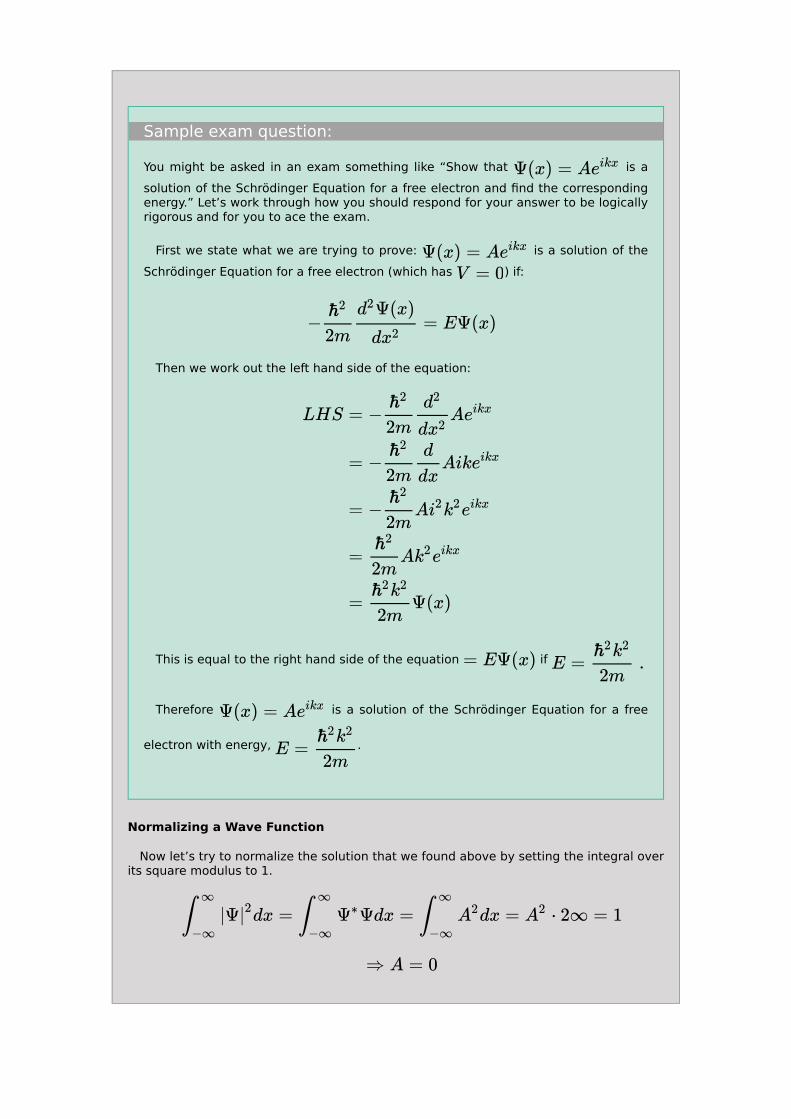
Sample exam question:
You might be asked in an exam something like “Show that is a solution of the Schrödinger Equation for a free electron and find the corresponding energy.” Let’s work through how you should respond for your answer to be logically rigorous and for you to ace the exam.
First we state what we are trying to prove: is a solution of the Schrödinger Equation for a free electron (which has ) if:
Then we work out the left hand side of the equation:
This is equal to the right hand side of the equation if
Therefore is a solution of the Schrödinger Equation for a free
electron with energy, .
Normalizing a Wave Function
Now let’s try to normalize the solution that we found above by setting the integral over its square modulus to 1.

We see that the mathematical solution has which means that the electron does not exist! While this is mathematically correct, it is clearly at best an unhelpful situation for understanding the properties of metals.
In fact in this (and other) case we need to also define the boundary conditions in order to obtain a physically meaningful, normalizable solution. In general we will see that two inputs are important for us to solve the Schrödinger Equation:
• the potential, . In the free electron case this is straightforward as . • the boundary conditions. Here it is not so clear; for a large system as
seems sensible, but mathematically it is impractical.
Next we will discuss suitable practical choices for the boundary conditions of a solid, and show how they lead to normalizability of the wavefunction. At this point we evolve from being mathematicians to being physicists!
Boundary Conditions
There are two widely-used choices for the boundary conditions (BCs) for a free electron in an infinite solid: The particle in a box and periodic boundary conditions.
1. Particle in a box
Here we assume that the electron is confined within a “box” of size so that it’s potential is zero for and infinite outside of that range (see Figure 3.1). (An analogous definition can be made for three dimensions.)
Figure 3.1 – Potential for a particle in a box of size L
To allow flexibility, we take as our trial wavefunction a linear combination of plane waves with positive and negative exponents, i.e. then we impose the BCs .
This gives us the solutions
with n=1,2,3,…
Normalization yields
and the resulting wave functions (shown in (Figure 3.2)) and energies are
; n=1,2,3…
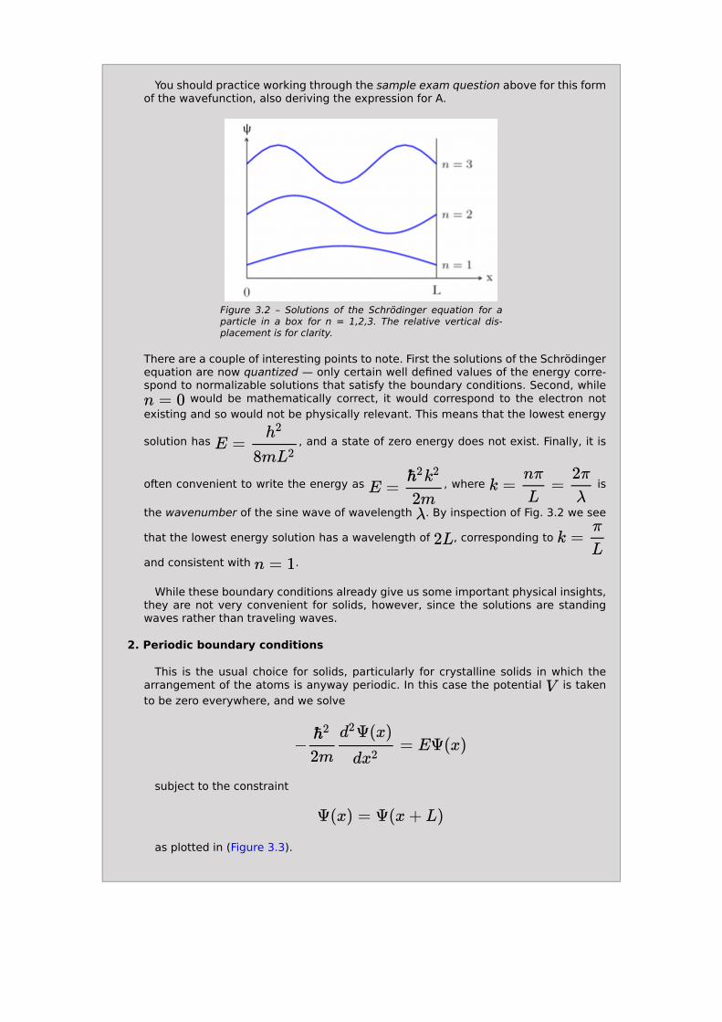
You should practice working through the sample exam question above for this form of the wavefunction, also deriving the expression for A.
Figure 3.2 – Solutions of the Schrödinger equation for a particle in a box for n = 1,2,3. The relative vertical dis-placement is for clarity.
There are a couple of interesting points to note. First the solutions of the Schrödinger equation are now quantized — only certain well defined values of the energy corre-spond to normalizable solutions that satisfy the boundary conditions. Second, while
would be mathematically correct, it would correspond to the electron not existing and so would not be physically relevant. This means that the lowest energy
solution has , and a state of zero energy does not exist. Finally, it is
often convenient to write the energy as , where is
the wavenumber of the sine wave of wavelength . By inspection of Fig. 3.2 we see
that the lowest energy solution has a wavelength of , corresponding to
and consistent with .
While these boundary conditions already give us some important physical insights, they are not very convenient for solids, however, since the solutions are standing waves rather than traveling waves.
2. Periodic boundary conditions
This is the usual choice for solids, particularly for crystalline solids in which the arrangement of the atoms is anyway periodic. In this case the potential is taken to be zero everywhere, and we solve
subject to the constraint
as plotted in (Figure 3.3).
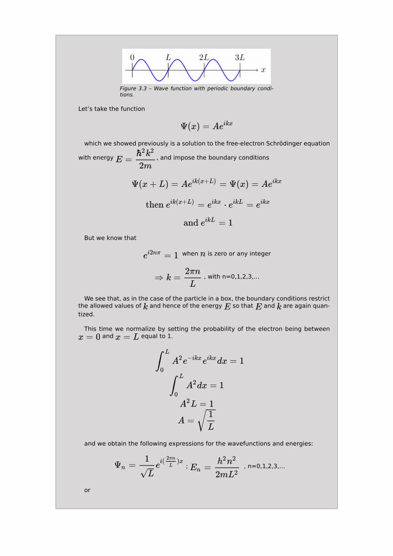
Figure 3.3 – Wave function with periodic boundary condi-tions.
Let’s take the function
which we showed previously is a solution to the free-electron Schrödinger equation
with energy , and impose the boundary conditions
But we know that
when is zero or any integer
, with n=0,1,2,3,…
We see that, as in the case of the particle in a box, the boundary conditions restrict the allowed values of and hence of the energy so that and are again quan-tized.
This time we normalize by setting the probability of the electron being between and equal to 1.
and we obtain the following expressions for the wavefunctions and energies:
; , n=0,1,2,3,…
or

; , , , …
In (Figure 3.4), we sketch the wavefunctions of the three lowest energy solutions. Immediately we see an important difference with the particle-in-a-box case: A zero energy state with , corresponding to a constant charge distribution with infi-nite wavelength, is in this case allowed. The next lowest energy wavefunction that
satisfies the boundary conditions (green line) is a sine wave with and
(the state). This has energy ; note that this is equal to
the energy of the state for a particle in a box of length , since the state for the particle in a box has only half a wavelength between
and . No states with wavelengths between 0 and “fit” with the period-ic boundary conditions; this is the origin of the quantization. As and the energy are increased, the wavelength of the wavefunction decreases, and the wavefunc-tion becomes more “wiggly” — in fact “wiggliness” is a sign of a high kinetic energy wavefunction.
Figure 3.4 – Solutions of the Schrödinger equation for a free electron with periodic boundary conditions. The boundary conditions constrain the allowed values of k and the energy of the wavefunctions.
Armed with our new quantum mechanics toolbox, let’s now calculate some properties of metals using quantum mechanical free electron theory, and compare them with experiment.
3.1 – Fermi Energy and Density of States Two quantities that we can both measure experimentally and calculate using quantum mechan-ical free electron theory are the Fermi energy, , and the density of states (DOS). We’ll remind ourselves of what these quantities are, and derive explicit expressions for them for the free-electron Fermi gas.
Density of States First the definition:

Definition: Density of States
The density of states, , is defined to be the number of states (in this case elec-tronic energy levels, ) per unit energy range
For the case of atoms or molecules, where the energy levels are isolated, the density of states consists of a function for each energy level. Below is the example for the molecular orbitals in the H2 molecule that are formed from the 1s atomic orbitals on the hydrogen atoms. There is one bonding orbital which is occupied by two electrons — we call this the highest occupied molecular orbital, or HOMO — separated by an energy gap from a higher lying empty orbital called the lowest unoccupied molecular orbital, or LUMO. To the right we show the density of states which is just a function at the energy values of each of the two orbitals.
Figure 3.5 – Energy level diagram and corresponding den-sity of states showing the bonding and anti-bonding orbital energy levels of molecular hydrogen. Occupied energy lev-els are highlighted in red.
While the density of states is not a terribly useful concept in the case where the energy levels are isolated, it is helpful for solids where the energy levels are so close together that they form effectively a continuous band. Let’s derive an expression for the density of states using our results for the solution of the Schrödinger equation for free electrons with periodic boundary conditions. We’ll make the derivation for the three dimensional case, where the quantization
condition is that in all three directions. Then the “volume” occupied by an electron-
ic state in -space is a cube with each edge length equal to which has volume .
Turning this around, the number of states per unit volume is levels; since each state
can take 2 electrons, of them are filled by the electrons. The electrons start filling the levels at the lowest energy ( ) first, then in order of increasing value. We call the wave vector at which we run out of electrons the Fermi wave vector, ; at this point the electrons
have filled a sphere in -space of radius and volume . We see that
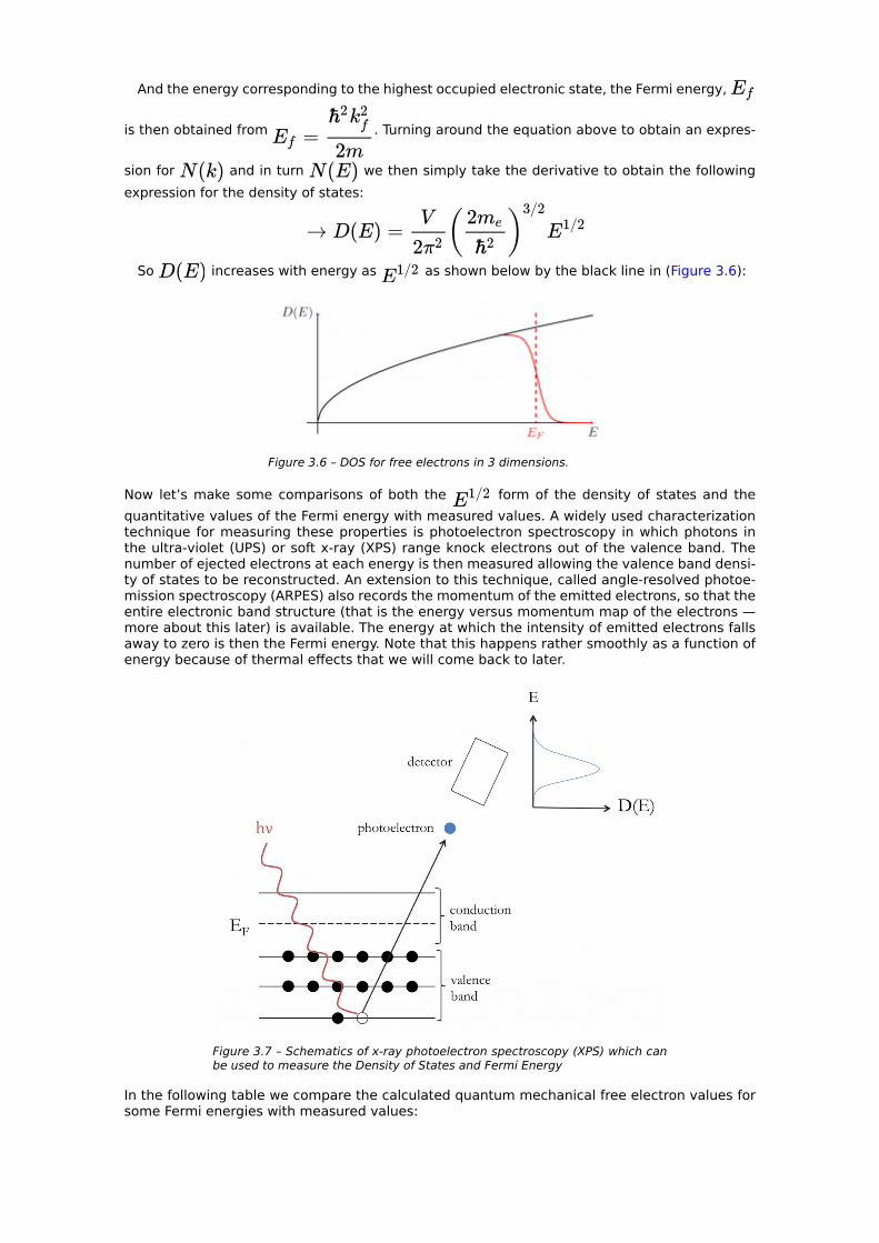
And the energy corresponding to the highest occupied electronic state, the Fermi energy,
is then obtained from . Turning around the equation above to obtain an expres-
sion for and in turn we then simply take the derivative to obtain the following expression for the density of states:
So increases with energy as as shown below by the black line in (Figure 3.6):
Figure 3.6 – DOS for free electrons in 3 dimensions.
Now let’s make some comparisons of both the form of the density of states and the quantitative values of the Fermi energy with measured values. A widely used characterization technique for measuring these properties is photoelectron spectroscopy in which photons in the ultra-violet (UPS) or soft x-ray (XPS) range knock electrons out of the valence band. The number of ejected electrons at each energy is then measured allowing the valence band densi-ty of states to be reconstructed. An extension to this technique, called angle-resolved photoe-mission spectroscopy (ARPES) also records the momentum of the emitted electrons, so that the entire electronic band structure (that is the energy versus momentum map of the electrons — more about this later) is available. The energy at which the intensity of emitted electrons falls away to zero is then the Fermi energy. Note that this happens rather smoothly as a function of energy because of thermal effects that we will come back to later.
Figure 3.7 – Schematics of x-ray photoelectron spectroscopy (XPS) which can be used to measure the Density of States and Fermi Energy
In the following table we compare the calculated quantum mechanical free electron values for some Fermi energies with measured values:
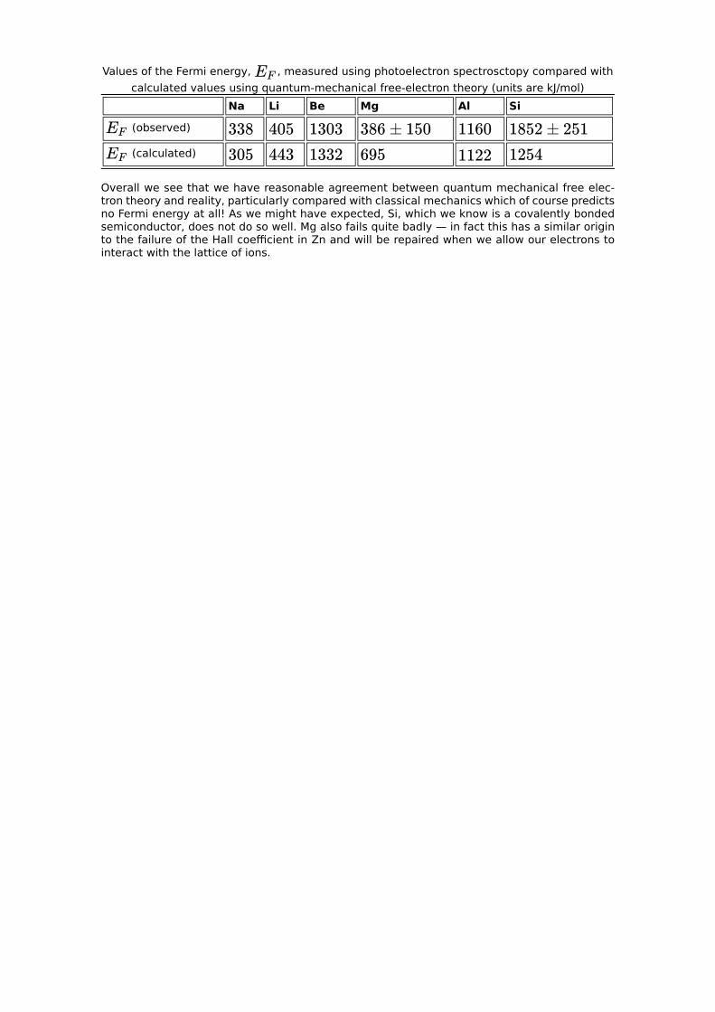
Values of the Fermi energy, , measured using photoelectron spectrosctopy compared with calculated values using quantum-mechanical free-electron theory (units are kJ/mol)
Na Li Be Mg Al Si
(observed)
(calculated)
Overall we see that we have reasonable agreement between quantum mechanical free elec-tron theory and reality, particularly compared with classical mechanics which of course predicts no Fermi energy at all! As we might have expected, Si, which we know is a covalently bonded semiconductor, does not do so well. Mg also fails quite badly — in fact this has a similar origin to the failure of the Hall coefficient in Zn and will be repaired when we allow our electrons to interact with the lattice of ions.

Review — Fermi statistics and chemical potential The Fermi-Dirac Distribution
At zero kelvin, all states below are filled, and all states above are empty. At temperatures above absolute zero, thermal energy promotes some of the electrons to states above the Fermi energy. Only those electrons close to can be promoted since there must be an empty state available.
We can use statistical mechanics to calculate the probability that an orbital at energy will be occupied at thermal equilibrium. The probability distribution is given by the Fer-mi-Dirac distribution:
is called the chemical potential and is equal to the derivative of the free energy with respect to the occupation of any energy level. From the equation above we see that the
chemical potential is the energy at which the probability of a state being occupied is .
At 0 K, .
Fermi Level versus Chemical Potential
The relationship , when is true for all temperatures.
The Fermi energy, , is only strictly defined at 0 K, where it is equal to the chemical potential, and marks the boundary between occupied and unoccupied energy lev-els. Often people use the chemical potential and the Fermi energy interchangeably, which is upsetting to true statistical mechanicians. However, as we can see in the plot below of the Fermi-Dirac distribution for a range of temperatures, it’s a pretty good approximation for temperatures below around 10’000K. Only at temperatures higher than this does the
point at which start to deviate from its low temperature value.
Figure 3.8 – Fermi-Dirac distribution function for various temperatures. The Fermi energy temperature (= Ef / kB) is set to 50’000 K (~ 4.3 eV) . The chemical potential at each temperature may be read off the graph as the energy at which f=0.5 .

Since in Materials Science we are usually interested in materials in the solid or liquid form (or at least almost always below 10,000 K!) our Fermi energies and chemical poten-tials are for practical purposes the same. So we are often a bit lazy and say that the Fermi
level is the state at which the probability of occupation is , writing
3.2 – Heat capacity revisited Finally, let’s return to the question of the heat capacity. Remember that in classical free elec-tron theory we overestimated the electron contribution to the heat capacity by about a factor of a hundred. However, in classical mechanics, where we have no Pauli principle, all of the elec-trons in the system were able to take up thermal energy and contribute to the heat capacity. As soon as we consider quantum mechanics we see that those electrons far below the Fermi energy can’t increase their energy when they are offered an additional of thermal energy because there is nowhere for them to go — the energy levels above them are already occu-pied with electorns and the Pauli principle prohibits adding more. Only those electrons within around of the Fermi energy are able to absorb thermal energy and contribute to the heat capacity; these are marked in yellow below.
Figure 3.9 – Density of states as a function of energy for QM free electrons with the fraction that are excitable by thermal energy shaded in yellow.
Let’s quantify this idea. The fraction of excitable electrons is roughly where
we define the characteristic temperature as
The number of excitable electrons per unit volume is then (where is the
number of electrons per unit volume) and each carries thermal energy of . So the total electronic thermal energy per unit volume is
The electronic contribution to the heat capacity is then given by
where the factor .

Now let’s look at some real heat capacity data and compare with the predicted values. If we had been a bit more careful with various factors in our derivation we would have obtained a
factor of rather than 2, so we define
Na Al Cu Co Ge Si (observed)
(calculated)
While the observed values for Na, Al and Cu are in good agreement with the calculations, the deviations for Co, Ge and Si are quite large. Certainly for Ge and Si we might have expected this as we know that they are not metallic. To describe insulating behaviour we will have to go one step further in our quantum mechanical development and include explicit interactions between the electrons and the lattice. It’s more unexpected that Co is a bad free-electron met-al in terms of its heat capacity, whereas Cu is good. Again we will need to go beyond free-elec-tron theory to explain this, and consider the atomic orbital nature of the electrons.
Missing Content Visit eskript.ethz.ch to see everything.
An interactive or media element has been excluded from this version of the text. You can view it online here: https://wp-prd.let.ethz.ch/WP0-CIPRF91184/?p=34
3.3 – Summary So how are we doing in describing reality with our theories so far? We saw that classical free electron theory correctly predicts Ohm’s law, as well as the Hall coefficients for some free-elec-tron metals. Its quantum-mechanical extension correctly describes the form of the density of states as well as the position of the Fermi energy and the heat capacity for those same free-electron metals.
We have some catastrophic failures, however, even among materials that we think of as good metals, such as the positive Hall coefficient of Zn and the heat capacity of cobalt. And we do not yet have the tools to describe insulating behaviour.
Our next extension will be to introduce interactions between the electrons and the ions in the material, and we will find that this simple step will recover much physical behaviour. But first a little bit of a quantum mechanical aside…

4
A little bit more quantum mechanics -- operators and measurements

Quantum mechanical concepts – Review II The Concept of Quantum Mechanical Operators
In quantum mechanics, things that we can measure, which we call observables are rep-resented by useful mathematical things called operators. Operators in quantum mechan-ics are chosen to satisfy the commutation relation:
which is famously known as the Heisenberg uncertainty principle. Here is the opera-tor for position and is the operator for momentum. The commutation relation is a basic, unproovable, underivable postulate that fits with measured reality. Our job is to choose expressions for the operators and to satisfy this commutation relation.
Let’s take multiply by position (for example in the direction, ). Then we
find that the momentum operator, . Let’s show this – it’s easier to keep
track of the derivatives if we operate on something, such as a wave function:
and
then
so
Note that this is just one choice of possible combinations of expressions for and that satisfies the uncertainty relation (it’s called the position representation) but is per-haps the most widely used, as it is rather intuitive to have the position operator be the physical position.
Now that we have operators for and we can construct operators for all dynamical variables, e.g. kinetic energy:
One slightly technical mathematical point: It turns out that all operators corresponding to physical observables in quantum mechanics have the mathematical property that they are Hermitian. This has a number of important implications all of which make our lives easier because their mathematics is well-behaved. We won’t go into the details, but might mention this property, and will certainly exploit it, throughout the course.
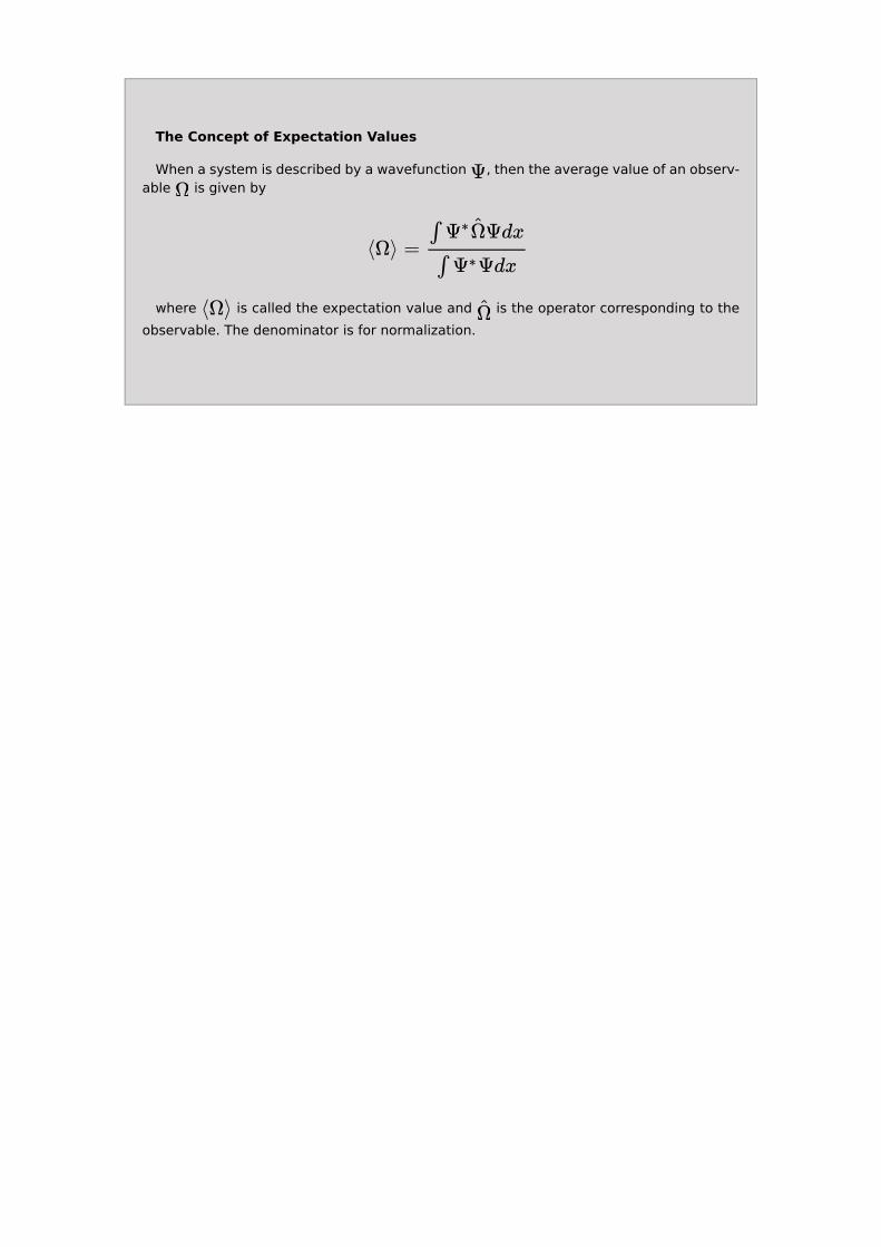
The Concept of Expectation Values
When a system is described by a wavefunction , then the average value of an observ-able is given by
where is called the expectation value and is the operator corresponding to the observable. The denominator is for normalization.

Exercise: Calculate , and for the “particle in a box”, that is for for
and outside of that range as shown below.
You might need the following identities:
Solution:
We know from our solution of the Schrödinger equation
with the “box” boundary conditions that
for n = 1,2,…
and
Working out the Expectation value for the energy we obtain:

Note that this is the same as our solution for the energy that we obtained using the Schrödinger equation. We could have anticipated this, as we know that the solu-tions of the Schrödinger equation have a well-defined value of their energy, and so their average energy must be equal to this — we will put this concept on a more formal footing in the next section.
Following the same procedure for the momentum, we obtain
Interestingly, the energy of the wavefunctions increases with but the momen-tum does not. This is because the wavefunctions are standing rather than traveling waves, so they carry no linear momentum. Finally, we obtain
The average value of the position is at the middle of the box. Note that this is not where the probability density is the maximum; we see for example that for the
and cases sketched below that this is zero at the middle of the box.
Formal Quantum Mechanical Measurement Theory
There is a fundamental difference between cases where the wavefunction is an eigen-function of the operator for the observable of interest i.e.
(e.g. )
and cases where it is not an eigenfunction. We see from the eigenvalue equation above that a wavefunction that is an eigenfunction of a particular operator remains unchanged, except for multiplication by a constant (the eigenvalue) when it is operated on by the operator. This has an important consequence: If a wavefunction is an eigenfunction of an operator , then every measurement of yields the same value . In the case when the wavefunction is not an eigenfunction, then different measurements yield different val-ues (each one being an eigenvalue), with the average of all the measurements being the expectation value.
For example, below we sketch the wavefunction , where and are the and solutions for the particle in a box.

Figure 4.3 – Two eigenfunctions: The blue curve is Ψ₁ (n=1) and the red one is Ψ₂ (n=1).
Figure 4.4 – The linear combination of the two eigenfunc-tions: The red curve is given by: Ψ =Ψ₁ + Ψ₂ which is a superposition of the two eigenfunctions but itself is not a eigenfunction.
If we then measure the energy of the wavefunction , the measured value will be half the time the energy of and the other half the energy of . On average, the ener-gy will be the expectation value of , but this number will never be obtained in a single measurement.
This concept is called the “generalized statistical interpretation”, which distinguishes two cases:
Case 1: is an eigenfunction of , then
An experiment to measure always gives the result .
Case 2: is NOT an eigenfunction of , but it can be expressed as a linear combina-tion of the eigenfunctions. (In fact this is always the case because the eigenfunctions of Hermitian operators form a complete set).

then
The expectation value is the weighted sum of the eigenvalues of ! And the contribu-tion of each eigenvalue to the expectation value is given by .

5
Summary
Now let’s see if you understood the relevant concepts of this first part of the book on electrical and thermal properties of metals!
Missing Content Visit eskript.ethz.ch to see everything.
An interactive or media element has been excluded from this version of the text. You can view it online here: https://wp-prd.let.ethz.ch/WP0-CIPRF91184/?p=40
Solution: Have a look after having first tried yourself above! • Ohm’s Law states that the resistance is independent of the applied voltage. • In the Drude model we assume that electrons are classical particles and that they do
not interact with each other either through collision or because of their charges. They only interact with ions by collisions like billiard balls.
• Classical free electron theory predicts ohmic behaviour! The thermal velocity is linearly proportional to the electric field, and therefore we know that the conductivity is a constant value.
• Hall effect measurements and real data from heat capacity values show the limits of the Drude model in explaining these two properties.
• In the Free Electron Fermi Gas model, electrons do not interact with each other or with ions, but they are described by quantum mechanics (Schrödinger equation and Pauli Principle).
• The Density of States D(E) is defined as the number of states per unit energy range. • The density of states D(E) for free electrons in 3 dimensions increases with the
square root of the energy. • The Fermi energy is the energy corresponding to the highest occupied electronic
state. • The calculated QM free electron values for Fermi energies correspond quite well to
the measured values except for the elements Si and Mg. • The Fermi-Dirac distribution defines the probability that an orbital at energy E will be
occupied at thermal equilibrium. • The real heat capacity data corresponds well to the calcaluated data using the QM
free electron model for metals but not for insulators. • Although the Free Electron Fermi Gas model explains more properties than the
classical model, interactions with the lattice will have to be included in order to make progress.
II
Solving the Schrödinger equation for an atom

6
Introduction
Rather than diving in directly to a full solution of a negatively charged electron attracted by a Coulomb potential to a positively charged ion, we will proceed by solving the Schrödinger equa-tion for a series of simpler situations, each of which introduce an additional degree of freedom and therefore an additional quantum number.
1. The “particle on a ring” , in which a free electron, with , is constrained by the boundary conditions to lie on a ring. The solution gives one quantum number:
2. The “particle on a sphere”, in which again the electron experiences zero potential, but this time the boundary conditions are chosen so that it lies on the surface of a sphere. This gives a second quantum number:
3. The “particle in a Coulomb potential”, for which the electron is no longer free, but feels the potential,
This gives one more quantum number: . These are the and quantum numbers that you are probably familiar with from the
description of atomic orbitals. Note that the spin quantum number, , is not obtained from a solution of the Schrödinger
equation. In this course we will add it as an extra quantum number without justification (beyond the slightly circular argument that it has to be there because of the Pauli principle). It does appear, however, as naturally as the and quantum numbers if one solves a relativistic extension of the Schrödinger equation called the Dirac equation in three dimensions and with appropriate boundary conditions.

7
Particle on a ring
We begin by solving the Schrödinger Equation for a free electron with and apply boundary conditions which constrain the particle to lie on a ring. While in principle one can do this in cartesian coordinates, life is much easier if we use polar coordinates as shown below:
Figure 7.1 – Definition of polar coordinates.
In polar coordinates the Laplacian is written as
n our case, is a constant and the wave function depends only on . So the terms with derivatives with respect to give zero when they operate on and the operator simplifies to
Then the Schrödinger Equation reads

We choose the boundary conditions so that when we make one complete circle around the ring, the wavefunction is identical to when we started — otherwise the wavefunction would interfere destructively with itself. Mathematically this means that
As before, we find the solution by inspection and write down
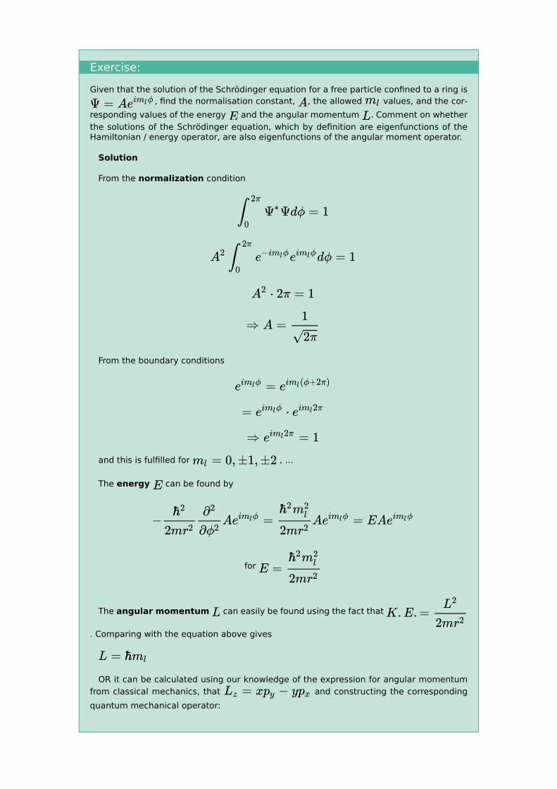
Exercise: Given that the solution of the Schrödinger equation for a free particle confined to a ring is
, find the normalisation constant, , the allowed values, and the cor-responding values of the energy and the angular momentum . Comment on whether the solutions of the Schrödinger equation, which by definition are eigenfunctions of the Hamiltonian / energy operator, are also eigenfunctions of the angular moment operator.
Solution
From the normalization condition
From the boundary conditions
and this is fulfilled for , …
The energy can be found by
for
The angular momentum can easily be found using the fact that
. Comparing with the equation above gives
OR it can be calculated using our knowledge of the expression for angular momentum from classical mechanics, that and constructing the corresponding quantum mechanical operator:

Then we calculate the expectation value of this operator using the wavefunction
Are the wavefunctions eigenfunctions of ?
Yes, with eigenvalue .
the quantum number indicates the z component of the angular momentum for
the wave function

8
Particle on a sphere
Our next step towards the full solution of the Schrödinger equation for an electron in a Coulom-bic potential is to solve the case of a free electron with the boundary conditions set so that it is confined to the surface of a sphere. Again, while we could in principle do this in cartesian coordinates, we will be happier if we use spherical coordinates as defined below:
then
Once again, since is fixed to the radius of the sphere, is a function of only, and
terms of the form and higher derivatives are zero. Then the Schrödinger equation is
The boundary conditions are such that when one goes all the way around the sphere back to the same point the wavefunction must be the same as that where one started. That is
.
This is an equation with known solutions, the spherical harmonics, which are listed in the table below, with and for the first few values of and . Notice that the dependent part, which is determined by the

quantum number has exactly the same form as the solutions for the particle on a ring. The new part of the wavefunction, which depends on the value, is described by a second quantum number which we usually call .
Spherical harmonics
It’s a good exercise to show that the energy, , is given by
Also the magnitude of the total angular momentum , is determined by the quantum number as follows:
and the component of angular momentum, as in the particle-on-a-ring case.

9
Particle in a coulombic 1/r potential
Now we progress to the full “hydrogen atom” problem, and rather than treating a free electron, we take the potential to be the Coulomb potential,
Note that the electron now has an additional degree of freedom, it can vary its value of , so we expect to obtain another quantum number. The Schrödinger equation is:
Again this is a standard equation with known solutions, which are the product of the spherical harmonics from the previous section and the associated Laguerre, functions
, given in the table
below. Hydrogenic radial wave functions
0 (1s)
0 (2s)
1 (2p)
0 (3s)
1 (3p)
2 (3d)
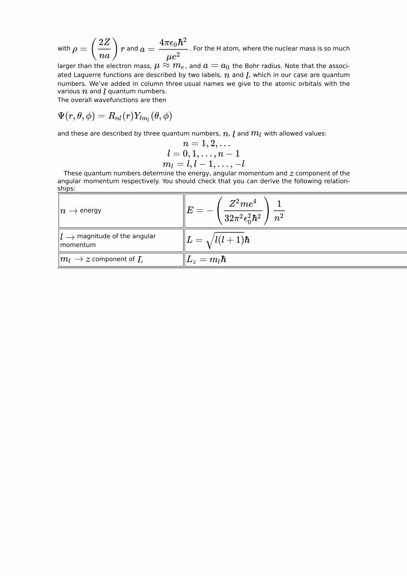
with and . For the H atom, where the nuclear mass is so much
larger than the electron mass, , and the Bohr radius. Note that the associ-ated Laguerre functions are described by two labels, and , which in our case are quantum numbers. We’ve added in column three usual names we give to the atomic orbitals with the various and quantum numbers. The overall wavefunctions are then
and these are described by three quantum numbers, , and with allowed values:
These quantum numbers determine the energy, angular momentum and component of the angular momentum respectively. You should check that you can derive the following relation-ships:
energy
magnitude of the angular momentum
component of

10
How do the quantum numbers correspond to the familiar atomic orbitals?
Each atomic orbital can be described by a specific set of quantum numbers. The quantum num-ber describes the shell and the possible values are … The quantum number describes the subshell and ranges from to , where corresponds to orbitals, to
orbitals, to orbitals and to orbitals. The possible values range from to , therefore for orbitals and for orbitals, etc.
While we saw in the previous section that the wavefunctions for the atomic orbitals are com-plex three-dimensional functions, often we sketch them using the “boundary surfaces” shown below.
Notice that, while the pz orbital has , the usual px and py orbitals sketched above do not correspond to well-defined values. Rather
Sometimes it is also useful to look at the radial part of the wavefunctions which are plotted as a function of below:
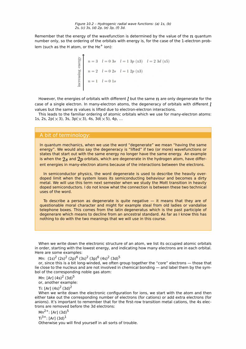
Figure 10.2 – Hydrogenic radial wave functions: (a) 1s, (b) 2s, (c) 3s, (d) 2p, (e) 3p, (f) 3d.
Remember that the energy of the wavefunction is determined by the value of the quantum number only, so the ordering of the orbitals with energy is, for the case of the 1-electron prob-lem (such as the H atom, or the He+ ion):
However, the energies of orbitals with different but the same are only degenerate for the case of a single electron. In many-electron atoms, the degeneracy of orbitals with different values but the same values is lifted due to electron-electron interactions.
This leads to the familiar ordering of atomic orbitals which we use for many-electron atoms: 1s, 2s, 2p( 3), 3s, 3p( 3), 4s, 3d( 5), 4p, …
A bit of terminology: In quantum mechanics, when we use the word “degenerate” we mean “having the same energy”. We would also say the degeneracy is “lifted” if two (or more) wavefunctions or states that start out with the same energy no longer have the same energy. An example is when the and orbitals, which are degenerate in the hydrogen atom, have differ-ent energies in many-electron atoms because of the interactions between the electrons.
In semiconductor physics, the word degenerate is used to describe the heavily over-doped limit when the system loses its semiconducting behaviour and becomes a dirty metal. We will use this term next semester when we study the Mott transition in heavily doped semiconductors. I do not know what the connection is between these two technical uses of the word.
To describe a person as degenerate is quite negative — it means that they are of questionable moral character and might for example steal from old ladies or vandalise telephone boxes. This comes from the latin degeneratus which is the past participle of degenerare which means to decline from an ancestral standard. As far as I know this has nothing to do with the two meanings that we will use in this course.
When we write down the electronic structure of an atom, we list its occupied atomic orbitals
in order, starting with the lowest energy, and indicating how many electrons are in each orbital. Here are some examples:
Mn: (1s)2 (2s)2 (2p)6 (3s)2 (3p)6 (4s)2 (3d)5 or, since this is a bit long-winded, we often group together the “core” electrons — those that
lie close to the nucleus and are not involved in chemical bonding — and label them by the sym-bol of the corresponding noble gas atom:
Mn: [Ar] (4s)2 (3d)5 or, another example: Ti: [Ar] (4s)2 (3d)2 When we write down the electronic configuration for ions, we start with the atom and then
either take out the corresponding number of electrons (for cations) or add extra electrons (for anions). It’s important to remember that for the first-row transition metal cations, the 4s elec-trons are removed before the 3d electrons:
Mn2+: [Ar] (3d)5
Ti3+: [Ar] (3d)1 Otherwise you will find yourself in all sorts of trouble.

11
The Schrödinger equation for the H₂ molecule
In the last section we solved the Schrödinger equation for the hydrogen atom and made an extension to many-electron atoms by taking the H atom solutions for the wavefunctions and energy levels and acknowledging that they should be changed a little bit because of the pres-ence of the other electrons.
Now let’s add a little bit more complexity — we’ll consider a molecule with more than one nucleus — and see how we get on with solving the Schrödinger equation. We’ll take the sim-plest possible example, the H2 molecule, and in fact will start with an even simpler case, the H2+ molecular ion, which has two nuclei but only one electron.
Figure 11.1 – Schematic of the H₂⁺ molecule consisting of two protons and one electron.
The Hamiltonian can be written as
(3.36)
This Hamiltonian depends on the coordinates of the electron and of both the ions, and so in principle is a many-body Hamiltonian. However, because the electron is so much lighter than the protons, on the time-scale of the electron whizzing around it sees the nuclei as effectively stationary. This allows us to make a simplification, called the Born-Oppenheimer-Approxima-tion (yes, the same Oppenheimer that ran the US nuclear weapons program during the 2nd world war) which separates out the motion of the nuclei from that of the electrons. We can then assume that constant on the time scale of the electron, and that
and depend only on the position of the electron.

Then the single electron experiences the potential , and we can
solve the resulting single-particle Schrödinger equation exactly, albeit numerically. The solution is shown below, calculated as a function of the spacing between the protons. Note that to obtain the total energy one takes the electron energy obtained from solution of the Schrödinger equation with the protons at fixed spacing, and adds to it the proton-proton repulsion energy,
.
Figure 11.2 – Total energy of the H2+ molecular ion as a function of spacing between the protons calculated as the sum of the electronic energy and the proton-proton repulsion e²/(4πε0R).
Next we consider the full H2 molecule problem, in which we have two electrons and two pro-
tons as sketched below.
Figure 11.3 – Schematic of the H₂ molecule consisting of two protons (1 and 2) and two electrons (eA and eB).
After making the Born-Oppenheimer approximation as before, the Hamiltonian is

(3.37) The last term of the potential energy is the Coulomb repulsion between the two electrons.
This couples and and prevents the separation of the Schrödinger equation into two sin-gle-electron Schrödinger equations. This many-body Schrödinger equation can not be solved directly and so approximations must be made. A widely used, successful approximation is the linear combination of atomic orbitals method which we introduce next.

12
Summary
Missing Content Visit eskript.ethz.ch to see everything.
An interactive or media element has been excluded from this version of the text. You can view it online here: https://wp-prd.let.ethz.ch/WP0-CIPRF91184/?p=56
Solution: Have a look after having first tried yourself above! • The characteristics of atomic orbitals can be reviewed using the solution of the
Schrödinger equation for an electron in a Coulomb potential. • The solution of the particle on a ring problem gives one quantum number: m. • The solutions of a particle on a sphere (spherical harmonics Y) are determined by 2
quantum numbers: l and m. • The solutions of the particle in a Coulomb potential (product of the spherical
harmonics Y and the associated Laguerre functions R) are determined by 3 quantum numbers: n, l and m, with certain allowed values.
• Each atomic orbital is described by a specific set of quantum numbers. For example, l=0 corresponds to s orbitals, 1 to p orbitals, 2 to d orbitals and 3 to f orbitals.
• As n increases for the same l, the spatial extent of the atomic orbital increases. • As l increases for a given n, the spatial extent of the atomic orbital decreases. • It is important to remember that in a transition metal ion, 4s electrons are removed
before 3d electrons. • According to the Born-Oppenheimer approximation, the motion of atomic nuclei and
electrons in a molecule can be separated.
III
Linear combination of atomic orbitals (LCAO)

13
Molecular orbitals from LCAOs
We’ll continue with our simplest possible example of the H2 molecule, and remind ourselves from our introductory chemistry class of what the molecular energy level diagram and orbitals look like. These are sketched below. We remember that the 1s orbitals of the two isolated hydrogen atoms interact to form a bonding molecular orbital (MO) of lower energy than the isolated atomic orbital (AO). The two electrons both go into this orbital giving an overall ener-gy lowering compared to the isolated atoms and stabilising the H2 molecule. A higher energy anti-bonding orbital is also formed which in the H2 ground state doesn’t contain any electrons.
Figure 13.1 – Left: Energy levels of the atomic and molecular orbitals of the H₂ molecule. Right: The linear combinations of atomic orbitals that make up the bonding and anti-bonding molecular orbitals.
If we want to calculate the energy of these molecular orbitals directly then we have to solve the many-body Schrödinger equation that we wrote down in the previous section which is real-ly difficult. But another approach is to take a guess at the wavefunctions, , of the molecular orbitals and then calculate their energies using the expression we learned last week for the expectation value:
So what might be good guesses for the MO wavefunctions? Well maybe you also remember from chemistry class that in the bonding MO the electrons pile up both around the atomic nuclei and in the region in between them — the simple argument that the negative charge of the elec-trons in between the positive nuclei pulls them together and stabilises the bond is often used. In the anti bonding MO, in contrast, the electrons stay away from the central region and remain closer to the nuclei — there is a node in the electronic wavefunction in between the nuclei. In the Figure above are sketches of molecular wave functions obtained by adding together the 1s
atomic orbital wavefunctions in phase with each other (i.e. ) and out
of phase (i.e. ). You can see that these linear combinations of atomic
orbitals look rather like our intuitive picture of the MOs of H2 and so we will use these as our starting point…
13.1 – Variation Method Next we will find the molecular orbitals and wavefunctions of the H2 molecule using a method called the variation method. In the variation method, one guesses an initial trial wavefunction (in this case we will guess a linear combination of atomic orbitals, LCAO) and then varies any adjustable parameters in the trial wavefunction — for example the coefficients in front of each

AO — to minimize the expectation value of the energy, . The variational principle, which we will derive later, tells us that when is at its minimum value, then the trial wave func-tion is as close as possible to the true , given the constraint of the form that was chosen for the trial wave function.
For the H2+ molecule, we take for our trial wavefunction, the linear combination of atomic orbitals of the 1s orbitals on each atom, and :
with
corresponding to the 1s orbital on atom 1 and on atom 2 respectively.
If we substitute this in our expression for and minimize the energy
by adjusting and , we find two solutions (we’ll come back to this and show it formally later):
A low energy solution, in which the two atomic orbitals are combined in phase, that is they
have the same coefficients, :
and a high energy solution:
Here
and
is sometimes called the Coulomb integral. It describes the energy of an electron sitting in an isolated atomic orbital .
Let’s look at :

is the wavefunction obtained when the full many-body Hamiltonian operates on .
The integral is called an overlap integral, and is equal to 1 if and 0 if
and are orthogonal, that is there is no similarity between them. is therefore often called a bond, transfer or resonance integral, as it indicates how similar becomes to after it is operated on by .
Note: are always negative, therefore the bonding orbital is lowered in energy by and the antibonding orbital is raised in energy by .
As the distance between the two orbitals increases, decreases and finally reaches zero when they are infinitely far apart. At this point, the molecular energies approach the ener-gy of the atomic orbitals of a H atom. The energies of the electronic energy levels look like this as a function of spacing between the atoms:
Figure 13.2 – Electronic energy as a function of R for the low (blue) and high (red) energy solutions.
To calculate the total energy, , we have to add the protons’ Coulomb repulsion energy to , which strongly increases as is reduced and becomes infinite as , so we obtain:
Figure 13.3 – Total energy as a function of R for the low (blue) and high (red) energy solutions.
For the electrons in the low energy, bonding molecular orbital, we see the characteristic mini-mum as a function of interatomic spacing, which corresponds to the bonding distance.

14
Formal statement and proof of the variational principle
Let’s assume a system that is described by a Hamiltonian which has a ground state with energy . The variation principle states that
for any trial wavefunction, , and that if is the true ground state wave function.
PROOF: We write the trial wavefunction as a linear combination of all of the solutions of the Schrödinger equation
(Note that this is always possible for Hermitian operators, because the basis of eigenfunc-tions is complete — this means that any general function can be written as a linear combina-tion of them. We also assume that the are chosen to be orthonormal, which again is always possible for the eigenfunctions of Hermitian operators. You will notice that quantum mechani-cians are much happier than most other scientists, who have to deal with non-Hermitian oper-ators). Now consider the integral
Now using the orthonormality condition that for and
for we obtain
(4.14) since and is non-negative. So
that is , which is what we set out to prove.

15
Application of the variational principle to the H₂ molecule
Taking
with , where is the 1s AO of atom 1 and 1s AO of atom 2, we obtain
with
To find the minimum in , we differentiate with respect to each coefficient in turn and set
in each case, giving
This is satisfied if both numerators = 0 i.e. if . These are called
the secular equations.
15.1 – How to Solve the Secular Equations We want to solve the secular equations
to find the coefficients . For the H2 molecule the secular equations are (writing out explicitly the terms rather than
keeping them in a summation): For :

For :
This is a system of linear equations, which in general is straightforwardly solved for the coefficients and by constructing a determinant as follows:
or in the case of the H2 molecule:
This is called the secular determinant. If the are orthonormal, then and for which simplifies our determinant to
(for fun you might want to work out the solution for the general case keeping the terms). Often one writes and so that
Solving the determinant equation gives two results for the energy for and for
, the familiar in-phase and out-of-phase linear combinations of atomic orbitals that we saw previously!

16
Other covalent diatomic molecules
We can use the concepts that we developed for the H2 molecule in the previous subsection to understand the electronic structure and stability of other covalent diatomic molecules. Let’s start with homonuclear diatomics, in which both atoms are the same.
We call the lowest energy MOs formed from the 1s AOs the 1 orbitals, with a indicating the anti bonding orbital. In the case of He2 (below left), which has 4 electrons, both the bond-ing 1 and anti-bonding 1 orbitals are filled. As a result there is no net gain in energy from the bond formation and He2 is not a stable molecule. (In fact if one keeps track of the terms in the secular equations, one finds that the anti-bonding MO increases its energy above that of the 1s AO a little bit more than the bonding MO lowers its energy giving a net energy cost to bond formation.)
Left: Energy level diagram for He2, which has an electronic structure like that of H2, but contains four electrons. Right: each interact with their counterparts on the neighboring atom giving two sets of molecular orbitals which we label
The next element in the periodic table, Li, has the electronic structure (1s)2 (2s)1 . In Li2 the 1s AOs interact to form 1 and 1 MOs as discussed above. In addition, the 2s AOs interact to form the bonding 2 and anti-bonding 2 molecular orbitals. The interaction between the 2s orbitals is stronger than that between the 1s orbitals because of their larger spatial extent. This in turn means that they have a larger which leads to a larger splitting. Note also that the number of MOs is always equal to the number of AOs, and that each MO can take two electrons which must have opposite spin.
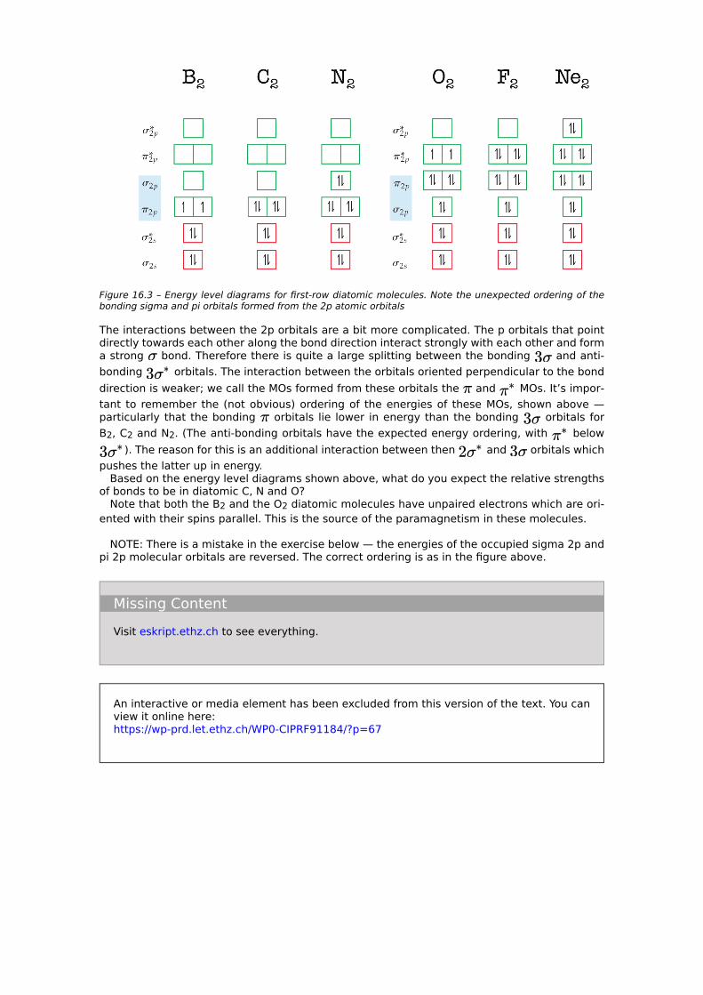
Figure 16.3 – Energy level diagrams for first-row diatomic molecules. Note the unexpected ordering of the bonding sigma and pi orbitals formed from the 2p atomic orbitals
The interactions between the 2p orbitals are a bit more complicated. The p orbitals that point directly towards each other along the bond direction interact strongly with each other and form a strong bond. Therefore there is quite a large splitting between the bonding and anti-bonding orbitals. The interaction between the orbitals oriented perpendicular to the bond direction is weaker; we call the MOs formed from these orbitals the and MOs. It’s impor-tant to remember the (not obvious) ordering of the energies of these MOs, shown above — particularly that the bonding orbitals lie lower in energy than the bonding orbitals for B2, C2 and N2. (The anti-bonding orbitals have the expected energy ordering, with below
). The reason for this is an additional interaction between then and orbitals which pushes the latter up in energy.
Based on the energy level diagrams shown above, what do you expect the relative strengths of bonds to be in diatomic C, N and O?
Note that both the B2 and the O2 diatomic molecules have unpaired electrons which are ori-ented with their spins parallel. This is the source of the paramagnetism in these molecules.
NOTE: There is a mistake in the exercise below — the energies of the occupied sigma 2p and
pi 2p molecular orbitals are reversed. The correct ordering is as in the figure above.
Missing Content Visit eskript.ethz.ch to see everything.
An interactive or media element has been excluded from this version of the text. You can view it online here: https://wp-prd.let.ethz.ch/WP0-CIPRF91184/?p=67

17
Heteronuclear diatomics and polar bonds (e.g. HF)
When the two atoms in a covalent bond are not the same, their on-site integrals, which we call or , are not the same, i.e. As a result the coefficients of their contribution
to the bonding and anti-bonding MOs are non longer equal, i.e. . Note, however, that
Bond formation can occur if the atomic orbitals have the correct symmetry and are close enough together so that is non-zero.
Lets skip the mathematics and just make a qualitative argument for the energy level diagram (NOTE: there should be a “proportional to” sign in front of both integrals!):
First we note that the outermost valence electron in an F atom sits in a 2p atomic orbital and so this is the orbital that is involved in bonding with the hydrogen 1s state. By symmetry, only the orbital pointing along the bond direction (which we label z) can form a bond; the integrals for the perpendicular p orbitals are zero by symmetry. Next we recognise that the F2pz atomic orbital is more electronegative than the H1s orbital and so its energy is correspondingly lower. As before, the AOs interact to form a bonding MO and an anti-bonding MO. The bonding orbital is lower in energy than the energy of the isolated F 2pz orbital by an amount that is proportional the size of the integral. The bonding MO is closer in energy to the F 2p level than to the H 1s level, therefore its wavefunction has a larger F 2p character (cF2p is greater than cH1s in the bonding orbital’s wavefunction). In contrast the the anti-bonding orbital, which is higher in energy than the energy of the H 1s orbital by an amount proportional to the integral, is closer in energy to the H1s AO and so its wavefunction has larger H1s amplitude (cH1s is greater than cF2p in the antibonding orbital’s wavefunction). The ratio of F to H charac-ter for the bonding molecule orbital, , indicating more electronic charge on the F ion. As a result HF has a electric dipole moment; another way to look at this is that the bond is partially ionic.

18
Summary
Missing Content Visit eskript.ethz.ch to see everything.
An interactive or media element has been excluded from this version of the text. You can view it online here: https://wp-prd.let.ethz.ch/WP0-CIPRF91184/?p=70
Solution: Have a look after having first tried yourself above! • The energy levels of molecular orbitals can be calculated from the linear combination
of atomic orbitals. • In the variation method, one guesses an initial trial wavefunction and then varies its
adjustable parameters to minimize the expectation value of the energy. • ß gives a measure of the interactions (overlap) between two atomic orbitals in the
environment of a molecule, and therefore it is 0 for orthogonal orbitals. • By solving the secular equations, one can find the energies for the combination of
atomic orbitals. • The molecular orbitals formed from the combination of s orbitals are called σ orbitals
(bonding and anti-bonding). • Interactions between p orbitals are more complicated. The p orbitals that point
directly towards each other along the bond direction interact strongly with each other and form a strong σ orbital. The interaction between the p orbitals oriented perpendicular to the bond direction is weaker. The molecular orbitals formed from these orbitals are the π orbitals.
• When the two atoms in a covalent bond are not the same, their on-site integrals (α) are not the same. As a result, their contribution to the bonding and anti-bonding molecular orbitals are no longer equal. The bonding molecular orbital will mostly present the character of the more electronegative atom.
• When extending LCAO theory to bands in solids, the band is then described by a Bloch function, which consists of the cell function multiplied by a complex exponential.
• The band structure shows the energy as a function of k. The bandwidth is then calculated as the difference in energy between the two extreme k values.

19
LCAO theory for solids
Remember that for the H2 molecule
Figure 19.1 – The two possible wave functions for the H₂ molecule.
the anti-bonding molecular orbital is formed from a linear combination of 1s atomic orbitals with opposite sign and the bonding molecular orbital from a linear combination of 1s orbitals with the same sign.
Let’s now make the extension from two to an infinite chain of H atoms with their 1s AOs (we consider the 1D case and write only the -dependence of the AOs for simplicity). By intelligent guessing, we can assume by analogy with H2 that the lowest energy LCAO has all of its coeffi-cients equal and with the same sign:
Figure 19.2 – Wave function of the bonding molecule orbital.
i.e. …
and the highest energy LCAO has all of its coefficients equal but alternating in sign
Figure 19.3 – Wave function of the antibonding molecule orbital.
i.e.
… Here is the atomic orbital at position , is the atomic orbital at position
and so on. We can rewrite those lowest and highest energy wave functions as
…
where is the atomic orbital at the position , the sum is over all atoms and
the wave vector is as usual .
The lowest energy case is then given by ( ) as then is always 1.
The highest energy case is given by ( ) because then is alternately plus 1
and -1 between adjacent atoms. While at the moment this might look like a rather silly mathe-matical overcomplication, we’ll see soon that it is actually a helpful general way of writing the wavefunction in a periodic solid. Those of you who remember coming across Bloch’s theorem previously might already appreciate the connection!
Now we want to find a general form for , not just the expression for the lowest and highest energy states. We use the fact that the properties of a crystal must have the same symmetry as the crystal (this is called Neumann’s principle). So, if the atoms repeat periodically with peri-odicity , as they do in our example, then the electron density must repeat periodically also, with the same periodicity. That is … This periodicity in the electron density (which remember is the square modulus of the electronic wavefunction) can only be achieved if the wavefunction has the following periodicity:
This in turn is achieved when for any value of , not just the two special cases that we considered above.
Hopefully you remember that a wavefunction that follows is called a Bloch function, which is often written in its more general form as
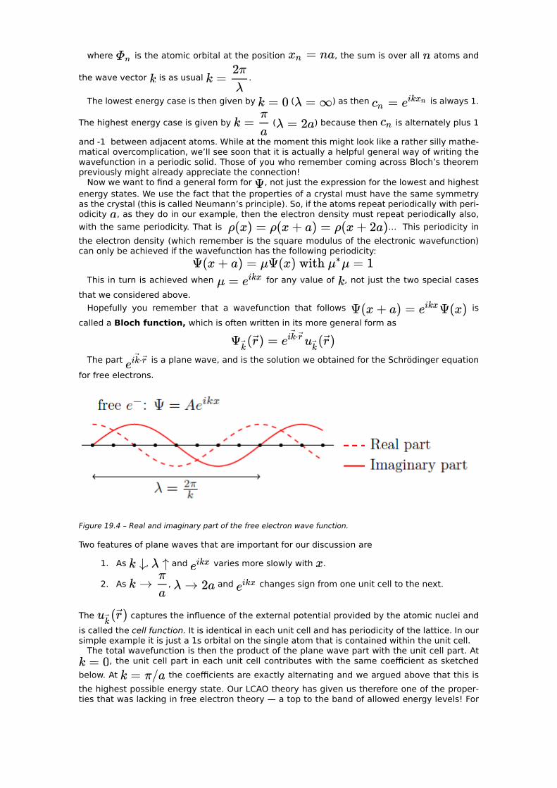
The part is a plane wave, and is the solution we obtained for the Schrödinger equation for free electrons.
Figure 19.4 – Real and imaginary part of the free electron wave function.
Two features of plane waves that are important for our discussion are
1. As , and varies more slowly with .
2. As , and changes sign from one unit cell to the next.
The captures the influence of the external potential provided by the atomic nuclei and is called the cell function. It is identical in each unit cell and has periodicity of the lattice. In our simple example it is just a 1s orbital on the single atom that is contained within the unit cell.
The total wavefunction is then the product of the plane wave part with the unit cell part. At , the unit cell part in each unit cell contributes with the same coefficient as sketched
below. At the coefficients are exactly alternating and we argued above that this is the highest possible energy state. Our LCAO theory has given us therefore one of the proper-ties that was lacking in free electron theory — a top to the band of allowed energy levels! For

intermediate k values the coefficients of the wavefunction evolve from one atom to the next as shown below — the wavelength of the “envelope function” is between 0 and and the energy is between that of the lowest and highest energy states.
Figure 19.5 – Bloch function for different k values.
Let’s work out the band width. To do this we’ll work out the energy as a function of the value, and see what range it spans.
Remember
so
and
We have chosen atoms instead of for mathematical simplicity. Then
(*) Now we make the assumptions that
, if
, if m,n are nearest neighbors, 0, otherwise. This means that only atoms that are adjacent interact with each other which is a very good
approximation in most cases. Then Eqn * simplifies to
(We used the orthonormality condition that if and other-
wise.)

Here’s what the band structure — that is the energy versus k diagram — looks like for a linear chain of H atoms each with a single s atomic orbital:
To find the bandwidth, we calculate the energy at the two extreme k values, 0 and and take
the difference; this gives the bandwidth of . Note that this result is for a 1D chain. In general the bandwidth also depends on the coordination number of the atoms in the solid because of the different numbers of nearest neighbours: Geometry Bandwidth
H2-molecule
1D chain
2D square lattice
3D simple cubic lattice
Next, let’s look at how this energy level diagram emerges from the molecular orbital diagram for a finite system. As an example, in the middle panel of the figure below we show the energy levels that are obtained by setting up the secular equations for a linear chain of eight atoms and assuming that only the nearest neighbours interact (in the exercises you will do this for a 3-atom chain which is less nasty mathematically). On the left those energies have been super-imposed as black dots on the band diagram for the infinite chain. We find that, even for 8 atoms we already recover the highest and lowest energy states, corresponding to the phases of the adjacent atomic orbitals always alternating or always being equal respectively. While in the case of a finite chain, the values strictly have no meaning, it’s helpful to think of the “wavelength” of the envelope function describing the alternation of the phases of the AOs as
. Then one finds that for the middle level, with energy , there are equal numbers of bond-
ing and anti-bonding interactions between adjacent orbitals giving overall what is called a non-bonding (i.e. not changed in energy from the atomic case) state. One can also see that there are two ways of achieving such a state which have equal energy, accounting for the double degeneracy.
19.1 – Beyond s orbitals — Interactions between atomic orbitals of different symmetry Next let’s extend the discussion to atomic orbitals of different symmetry, for example p orbitals, and work out the nature of the band dispersion by analysing the interactions between the AOs pictorially. Remember that at each unit cell is identical, whereas at

the orbitals in adjacent unit cells alternate in sign. For the case of s orbitals this makes the state the lowest in energy, and the the highest, but what about for the p
orbitals? Let’s take a look:
Figure 19.7 – Relative orientations of s and p orbitals at k=0 and k=π/a, giving rise to bonding and antibond-ing combinations.
From examining the cartoons above we find that • for bonds between p orbitals (that is when the orbitals are oriented along the bond
direction), we have the opposite behaviour from the s orbitals — the most bonding state is found at and the most anti-bonding at . This means that
the bands disperse (that is they evolve as a function of ) in the opposite direction
along the energy axis. Mathematically, between orbitals
pointing along the bond direction has the opposite sign from • for bonds between p-orbitals (that is when the orbitals are oriented perpendicular
to the bond direction), the behaviour is the same as for the s orbitals, with the most bonding state at and the most anti-bonding at . therefore has
the same sign as .
19.2 – Band Structure of a 2D Lattice of p-Orbitals Now we are in a position to work out the band structure for a more complicated case, a 2D lattice of px and py orbitals in the x-y plane. First let’s sketch the arrangement of the atomic orbitals at the extreme points, that is (the phases of adjacent orbitals

are identical in both directions), (the phases of adjacent orbitals alter-
nate in the x direction but are identical in the y direction) and (the
phases of adjacent orbitals alternate in both directions). We’ll do it for the py orbitals.
Figure 19.8 – Variation of bonding and antibonding in a 2-dimensional array of pσ and pπ orbitals.
We see that at , the system is bonding in both the and the direc-
tions, and so this is the lowest energy state. At , the system is bond-ing in the direction but anti-bonding in the direction, and so is higher energy than at
. Finally, at , we are anti-bonding in both directions indicating
the highest energy state. To be able to sketch the band diagram, we need to recognise that image \beta_{\pi}" title="\beta_{\sigma} > \beta_{\pi}" class="latex mathjax"> since the -orbitals are pointing directly to each other, which results in a stronger interaction. So an ab
arrangement increases the energy more than an ab arrangement relative to the bonding state. In Fig. 18.8 we sketch the approximate dispersion curve (assuming cosine behaviour in between the band edges).
In the following interactive module you can work out the behaviour of a 2D lattice of px orbitals.
Missing Content Visit eskript.ethz.ch to see everything.
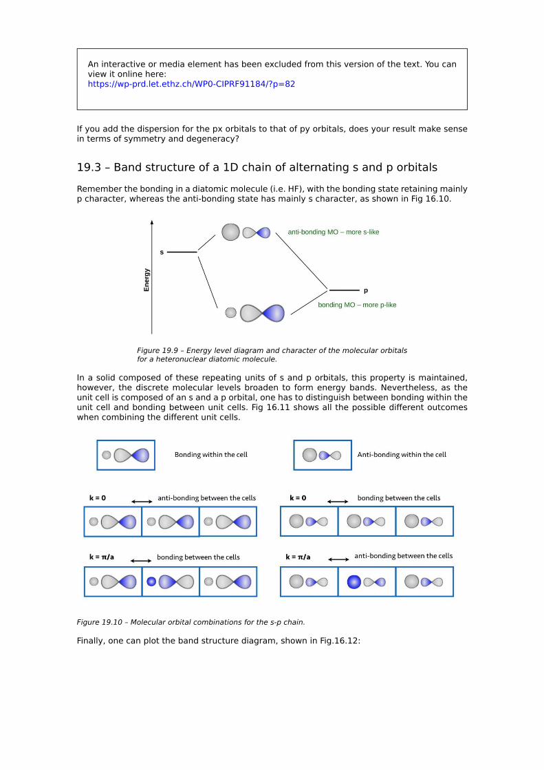
An interactive or media element has been excluded from this version of the text. You can view it online here: https://wp-prd.let.ethz.ch/WP0-CIPRF91184/?p=82
If you add the dispersion for the px orbitals to that of py orbitals, does your result make sense in terms of symmetry and degeneracy?
19.3 – Band structure of a 1D chain of alternating s and p orbitals Remember the bonding in a diatomic molecule (i.e. HF), with the bonding state retaining mainly p character, whereas the anti-bonding state has mainly s character, as shown in Fig 16.10.
Figure 19.9 – Energy level diagram and character of the molecular orbitals for a heteronuclear diatomic molecule.
In a solid composed of these repeating units of s and p orbitals, this property is maintained, however, the discrete molecular levels broaden to form energy bands. Nevertheless, as the unit cell is composed of an s and a p orbital, one has to distinguish between bonding within the unit cell and bonding between unit cells. Fig 16.11 shows all the possible different outcomes when combining the different unit cells.
Figure 19.10 – Molecular orbital combinations for the s-p chain.
Finally, one can plot the band structure diagram, shown in Fig.16.12:

Figure 19.11 – Band structure diagram for the diatomic s-p chain.
19.4 – Exercises: Click on the ? signs in the following chart to reveal a picture of a band structure or a figure cap-tion describing the band structure. Match the correct figures with the corresponding captions as quickly as you can!
Missing Content Visit eskript.ethz.ch to see everything.
An interactive or media element has been excluded from this version of the text. You can view it online here: https://wp-prd.let.ethz.ch/WP0-CIPRF91184/?p=82
Missing Content Visit eskript.ethz.ch to see everything.
An interactive or media element has been excluded from this version of the text. You can view it online here: https://wp-prd.let.ethz.ch/WP0-CIPRF91184/?p=82

Missing Content Visit eskript.ethz.ch to see everything.
An interactive or media element has been excluded from this version of the text. You can view it online here: https://wp-prd.let.ethz.ch/WP0-CIPRF91184/?p=82

IV
Using bandstructures to understand and explain the properties of solids
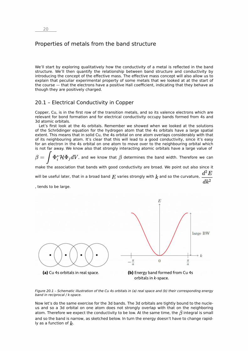
20
Properties of metals from the band structure
We’ll start by exploring qualitatively how the conductivity of a metal is reflected in the band structure. We’ll then quantify the relationship between band structure and conductivity by introducing the concept of the effective mass. The effective mass concept will also allow us to explain that peculiar experimental property of some metals that we looked at at the start of the course — that the electrons have a positive Hall coefficient, indicating that they behave as though they are positively charged.
20.1 – Electrical Conductivity in Copper Copper, Cu, is in the first row of the transition metals, and so its valence electrons which are relevant for bond formation and for electrical conductivity occupy bands formed from 4s and 3d atomic orbitals.
Let’s first look at the 4s orbitals. Remember we showed when we looked at the solutions of the Schrödinger equation for the hydrogen atom that the 4s orbitals have a large spatial extent. This means that in solid Cu, the 4s orbital on one atom overlaps considerably with that of its neighbouring atom. It’s clear that this will lead to a good conductivity, since it’s easy for an electron in the 4s orbital on one atom to move over to the neighbouring orbital which is not far away. We know also that strongly interacting atomic orbitals have a large value of
, and we know that determines the band width. Therefore we can
make the association that bands with good conductivity are broad. We point out also since it
will be useful later, that in a broad band varies strongly with and so the curvature,
, tends to be large.
Figure 20.1 – Schematic illustration of the Cu 4s orbitals in (a) real space and (b) their corresponding energy band in reciprocal / k-space.
Now let’s do the same exercise for the 3d bands. The 3d orbitals are tightly bound to the nucle-us and so a 3d orbital on one atom does not strongly overlap with that on the neighboring atom. Therefore we expect the conductivity to be low. At the same time, the integral is small and so the band is narrow, as sketched below. In turn the energy doesn’t have to change rapid-ly as a function of .

Figure 20.2 – Schematic illustration of the Cu 3d orbitals in (a) real space and (b) their corresponding energy band in reciprocal / k-space.
From our analysis we can say therefore that narrower bands, with a smaller curvature, ,
have lower conductivity.
20.2 – The Effective Mass Now we will formalize the link between the band structure and the conductivity using the con-cept of the effective mass. We remember that for free electrons, the energy is given by
so that
This equation implies that the curvature of the energy as a function of is determined by the electronic mass. Alternatively we can write that
This doesn’t buy us much for a free electron, we’ve just gone around in a circle. When we apply free-electron theory to the electrons in solids, however, we find that, while the energy is indeed
often (at least in good “free-electron” solids) proportional to , the curvature, , can be
different in different materials. Therefore we define an effective mass, , as

where is the actual curvature of the band in the real material. We find that defined
in this way gives a good description of the conductivity of the electrons in the solid. Remember of course that the mass of each individual electron has not changed; this is still a fundamental constant that we can’t modify. But because the electrons are not actually free but in reality interact with each other and the ions, they behave like free electrons but with a different mass! We see therefore that even at the free-electron theory level, we actually cheated and already incorporated some aspects of the interaction with the lattice, and the interactions with other electrons through this renormalization of the electron mass.
20.3 – Response of an Electron in a Solid to an Electric Field Now let’s see how renormalizing the mass of the electrons affects things physically when we apply an electric field, . We can combine Newton’s law that with the basic elec-trostatic law that (the minus sign is because the electron charge is negative) to obtain an expression for the acceleration of an electron, , in the presence of the field:
So we see that a negatively charged electron with a positive effective mass is accelerated in the opposite direction to that in which the electric field is applied. We used this result earlier of course in the derivation of the Hall effect and Hall coefficients.
Now let’s re-examine this result with our new understanding of the concept of effective mass. At the bottom of the s and d energy bands, the curvature and hence are indeed positive,
and so has the same sign as for a free electron. Therefore when the Fermi energy lies
towards the bottom of the band, the electrons that are relevant for conductivity are indeed accelerated by an electric field in the direction that we would expect for a negatively charged particle.
Figure 20.3 – Simple band diagram indicating regions of positive and negative effective mass.
Near the top of the band, however, we see that the curvature and hence are negative, and
so has the opposite sign from that of a free electron. Therefore the particle (in fact we
call it a “quasi-particle”) consisting of an electron interacting with all of the other electrons and the ions in the solid is accelerated in the opposite direction from that of a free electron.
Since it is a bit difficult conceptually to think of the electron as having negative mass, and all that we can measure experimentally is the ratio of mass and charge, we choose to keep the mass positive which we can do by changing the sign of the charge. We think of the current at

the top of the valence band as being carried by positively charged holes having positive mass. This is the origin of the positive which we obtained for example in metals such as Zn, for which the lies near the top of the band.
We can also see that the effective masses of electrons near the band edges in the s band are smaller than those in the d band. This is consistent with our earlier argument that conductivity is better in the s band than in the d band.
Notice that if the Fermi energy lies say halfway up the band, the dispersion relation, that is , is not quadratic. In this region it does not make sense to talk about the effective mass,
which is only defined in regions where the energy depends quadratically (or close to quadrat-ically) on the energy. Other interesting things happen in this situation, though, which we will come to later…
Quantum Mechanical Concepts – Momentum of Bloch Function Remember that the wavefunction of an electron in a periodic solid can be written as a Bloch function which is the product of a plane wave and a “unit cell” function that repeats periodically. In the 1D case it looks like this:
Remember also that the wavelength of the plane wave is given by .
Then we can use the de Broglie formula that the momentum to write down that
the momentum of our Bloch function is given by . We call this quantity the crys-tal momentum: we saw in the previous section how the value influences the response of a Bloch electron to an applied field.
Let’s calculate for a Bloch function to see if a Bloch function is also an eigenfunc-tion of the momentum operator with eigenvalue . We obtain
This is equal to only if which in general is not the case. So a Bloch
function is not an eigenfunction of the momentum operator with this value as its eigen-value and therefore is not strictly a momentum for a Bloch electron.
In the case of a free electron, with , there is no “unit-cell” part because the electron does not interact with the lattice and
So the free electron wavefunctions are eigenfunctions of the momentum operator, and their eigenvalues are true momenta.
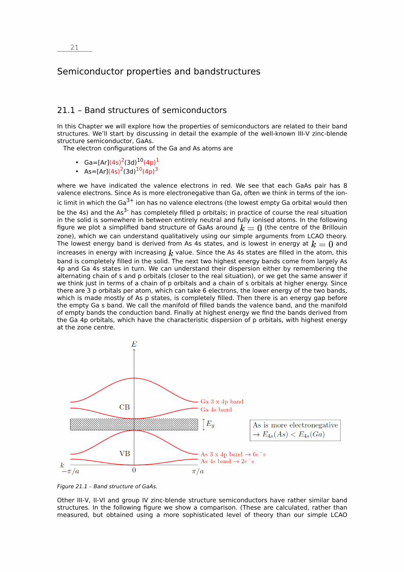
21
Semiconductor properties and bandstructures
21.1 – Band structures of semiconductors In this Chapter we will explore how the properties of semiconductors are related to their band structures. We’ll start by discussing in detail the example of the well-known III-V zinc-blende structure semiconductor, GaAs.
The electron configurations of the Ga and As atoms are
• Ga=[Ar](4s)2(3d)10(4p)1
• As=[Ar](4s)2(3d)10(4p)3
where we have indicated the valence electrons in red. We see that each GaAs pair has 8 valence electrons. Since As is more electronegative than Ga, often we think in terms of the ion-ic limit in which the Ga3+ ion has no valence electrons (the lowest empty Ga orbital would then be the 4s) and the As3- has completely filled p orbitals; in practice of course the real situation in the solid is somewhere in between entirely neutral and fully ionised atoms. In the following figure we plot a simplified band structure of GaAs around (the centre of the Brillouin zone), which we can understand qualitatively using our simple arguments from LCAO theory. The lowest energy band is derived from As 4s states, and is lowest in energy at and increases in energy with increasing value. Since the As 4s states are filled in the atom, this band is completely filled in the solid. The next two highest energy bands come from largely As 4p and Ga 4s states in turn. We can understand their dispersion either by remembering the alternating chain of s and p orbitals (closer to the real situation), or we get the same answer if we think just in terms of a chain of p orbitals and a chain of s orbitals at higher energy. Since there are 3 p orbitals per atom, which can take 6 electrons, the lower energy of the two bands, which is made mostly of As p states, is completely filled. Then there is an energy gap before the empty Ga s band. We call the manifold of filled bands the valence band, and the manifold of empty bands the conduction band. Finally at highest energy we find the bands derived from the Ga 4p orbitals, which have the characteristic dispersion of p orbitals, with highest energy at the zone centre.
Figure 21.1 – Band structure of GaAs.
Other III-V, II-VI and group IV zinc-blende structure semiconductors have rather similar band structures. In the following figure we show a comparison. (These are calculated, rather than measured, but obtained using a more sophisticated level of theory than our simple LCAO

method). As we move down the columns of the figure we move down in the periodic table, and as we move from left to right, we change from group IV to III-V to II-VI within the same row of the periodic table.
Figure 21.2 – A comparison of “real” (calculated using sophisticated theories) band structures for group IV, III-V and II-VI semiconductors.
We see a number of trends in the band structures both as the atoms get heavier and the bonds become more ionic.
First, we see that the band gap decreases as we move down the periodic table. For example, the band gaps for the group IV materials are given in the table below. We can understand this trend by recognising that, as one moves down the periodic table, the larger outermost atomic orbitals overlap more strongly and the bandwidths become wider. Wider bands in turn lead to a narrower band gap. In addition, as one moves to higher quantum number, the separation between the energy levels in an atom and in turn the bands in a solid becomes smaller; this factor also leads to narrower band gaps. By the time we reach lead the bands are overlapping so that the gap is zero and lead is metallic.
Band gap [eV] Electron configuration
C 5.5 (1s)2(2s)2(2p)2
Si 1.1 [Ne](3s)2(3p)2
Ge 0.7 [Ar](3d)10(4s)2(4p)2
Sn metallic ( ), 0.1 ( ) [Kr](4d)10(5s)2(5p)2
Pb metallic
From left to right the ionicity increases and the band gap increases. This is because more ionic bonds are less covalent which means that the integrals are smaller and the bands are nar-row. And again, narrower bands have larger band gaps between them. Below are the values for the fourth row elements.
Ionicity Band gap [eV]

Ge not ionic 0.7
GaAs a bit ionic 1.5
ZnSe more ionic 2.8
The small splitting at the top of the valence band at the point ( ) between the light (large curvature) and heavy (small curvature) holes increases as we move down the periodic table. This splitting comes from the spin-orbit coupling, which is larger for heavier atoms.
Next we will look at how these trends in band structure with crystal chemistry manifest in an important property of semiconductors, the optical absorption.
21.2 – Optical Absorption Here we will discuss the connection between the band structure and the optical absorption, specifically when an incoming photon excites an electron from the valence band to the conduc-tion band and is absorbed during the process.
The first factor which determines the optical absorption spectrum is the band gap. Since overall energy must be conserved, if the photon energy is smaller than the band gap, then it is insufficient to promote even the topmost electron in the valence band up into the conduction band, and so no absorption can occur. The absorption onset is therefore set by the size of the band gap.
The second important factor results from conservation of momentum. Remember that we showed that the momentum of an electron is determined by its value. Since the momentum of a photon is very small, this means that the value of the electron should be the same in its ground and excited states if a photon is making the excitation. This leads to the “selection rule” for optical transitions that , that is the transitions must be “vertical” within the band structure. As a result, two qualitatively different absorption behaviours are found in semi-conductors. When the values at the top of the valence band and bottom of the conduction band are equal (this usually occurs at ), there is a sharp onset of absorption exactly when the photon energy becomes equal to the band gap energy. The absorption profile then increases in the same manner as the density of available states, that is as . We call such materials direct gap semiconductors (see figure below).

When the top of the valence band and bottom of the conduction band are at different points in space, the absorption onset takes place in two steps:
1. Absorption of a photon with a vertical transition to a “virtual state” in the gap whose energy is close to that of the bottom of the conduction band
2. Emission or absorption of a phonon / lattice vibration which has only a very small energy, , but a large momentum, , equal to the difference in value between the band edges.
This two-step process (see figure above) allows for conservation of both energy and momen-tum. Since a two-step process of course has a lower probability than a single process, however, the absorption is weak until the energy corresponding to the lowest direct transition is reached (see figure below).
Figure 21.4 – Absorption spectrum of an indirect gap material. The onset of direct transitions occurs at energies higher than the band gap energy, Eg.
We call such materials indirect gap semiconductors. In addition to the band gap, two other features of the band structure are important in deter-
mining the optical absorption at a particular energy/frequency:
21.2.1 – The joint density of states Clearly the intensity of the optical absorption depends both on how many electrons are avail-able to be excited and how many empty states are available to accept them. This quantity, which is a function of energy, is called the joint density of states, and mathematically this is given by the convolution of the valence band states with the conduction band states.
Below is an example of a convolution between two gaussians, the result of which is also a gaussian:
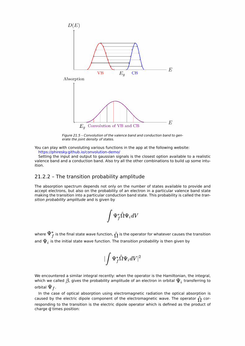
Figure 21.5 – Convolution of the valence band and conduction band to gen-erate the joint density of states.
You can play with convoluting various functions in the app at the following website: https://phiresky.github.io/convolution-demo/ Setting the input and output to gaussian signals is the closest option available to a realistic
valence band and a conduction band. Also try all the other combinations to build up some intu-ition.
21.2.2 – The transition probability amplitude The absorption spectrum depends not only on the number of states available to provide and accept electrons, but also on the probability of an electron in a particular valence band state making the transition into a particular conduction band state. This probability is called the tran-sition probability amplitude and is given by
where is the final state wave function, is the operator for whatever causes the transition and is the initial state wave function. The transition probability is then given by
We encountered a similar integral recently: when the operator is the Hamiltonian, the integral, which we called , gives the probability amplitude of an electron in orbital transferring to orbital .
In the case of optical absorption using electromagnetic radiation the optical absorption is caused by the electric dipole component of the electromagnetic wave. The operator cor-responding to the transition is the electric dipole operator which is defined as the product of charge times position:

if the light is polarised in the x direction. The transition probability amplitude is then given by
Here the integral tells us the probability amplitude of the electron transferring between the two orbitals when it is operated on by the dipole operator.
Note that this integral is only non-zero when (and , because oth-erwise the integral over the product of the oscillating part with will always yield zero. So we find the same result from symmetry considerations that we already knew from conservation of momentum: that the transition probability amplitude (TPA) is only non-zero and a transition can occur only when , i.e. only vertical transitions in the band structure are allowed.
In the case when is satisfied there are still additional symmetry considerations that might make the transition probability zero. Let’s look at the “surviving” part of the transition probability amplitude in this case:
We’ll use symmetry to analyse cases for which this integral is zero. First imagine that the top of the valence band and the bottom of the conduction band are both made up of bands derived from s orbitals, for example the 1s and the 2s:
Figure 21.6 – Wave functions of 1s and 2s orbitals and representation of the position operator x̂.

Since the the 1s and 2s orbitals are symmetric functions, whereas the operator is anti-
symmetric, the integral is zero by symmetry. Therefore the optical
absorption is zero if both the occupied and empty orbitals are derived from s orbitals! We would obtain the same result by the same argument if both orbitals were p orbitals.
For the case in which is a band derived from p orbitals and from s orbitals, however,
then the product is symmetrical and is non-zero. (We’ve seen
already that this combination is usual in zincblende structure semiconductors).
Figure 21.7 – Wave functions of p and s orbitals and representation of the position operator.
This symmetry restriction on the transition probability amplitude is a manifestation of parity conservation: Inversion symmetric orbitals, such as s and d, have even parity (sometimes written as ), antisymmetric orbitals such as p orbitals as well as photons have odd parity (sometimes written as ), and overall the parity of the whole system must be conserved during a transition.
parity conservation s-orbital even parity p-orbital odd parity photon odd parity
Note that for a particular pair of bands, the transition probability amplitude is approximately constant as a function of , therefore the shape of the absorption spectrum the joint DOS.
In summary, we find that optical transitions must: • conserve energy • conserve • conserve parity
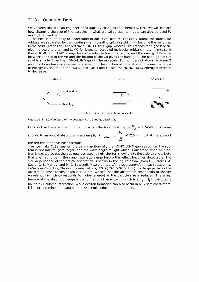
21.3 – Quantum Dots We’ve seen that we can engineer band gaps by changing the chemistry. Here we will explore how changing the size of the particles in what are called quantum dots can also be used to modify the band gap.
The idea is quite easy to understand in our LCAO picture. For just 2 atoms the molecular orbitals are separated by the bonding — anti-bonding splitting which will become the band gap in the solid. (Often this is called the “HOMO-LUMO” gap, where HOMO stands for highest occu-pied molecular orbital, and LUMO for lowest unoccupied molecular orbital). In the infinite solid these HOMO and LUMO energy levels broaden to form the bands, and the energy difference between the top of the VB and the bottom of the CB gives the band gap. The band gap in the solid is smaller than the HOMO-LUMO gap in the molecule. For numbers of atoms between 2 and infinity we have an intermediate situation: The addition of more atoms broadens the range of energy levels around the HOMO and LUMO and causes the HOMO-LUMO energy difference to decrease.
Figure 21.8 – LCAO picture of the change of the band gap with size.
Let’s look at the example of CdSe, for which the bulk band gap is = 1.74 eV. This corre-
sponds to an optical absorption wavelength, of 710 nm, just at the edge of
the red end of the visible spectrum. As we make CdSe smaller, the band gap (formally the HOMO-LUMO gap as soon as the sys-
tem is not infinite) gets larger, and the wavelength of light which is absorbed when an elec-tron is excited across the gap gets correspondingly shorter, moving into the visible range. Note that one has to be in the nanometer-size range before this effect becomes detectable. The size dependence of the optical absorption is shown in the figure below (from D. J. Norris, A. Sacra, C. B. Murray, and M. G. Bawendi, Measurement of the size dependent hole spectrum in CdSe quantum dots, Physical Review Letters, 72(16):2612-2615, Link). For large particles the absorption onset occurs at around 700nm. We see that the absorption onset shifts to shorter wavelength (which corresponds to higher energy) as the particle size is reduced. The sharp feature at the absorption edge is the formation of an exciton, which is an pair that is bound by Coulomb interaction. While exciton formation can also occur in bulk semiconductors, it is more prominent in nanometer-sized semiconductor quantum dots.
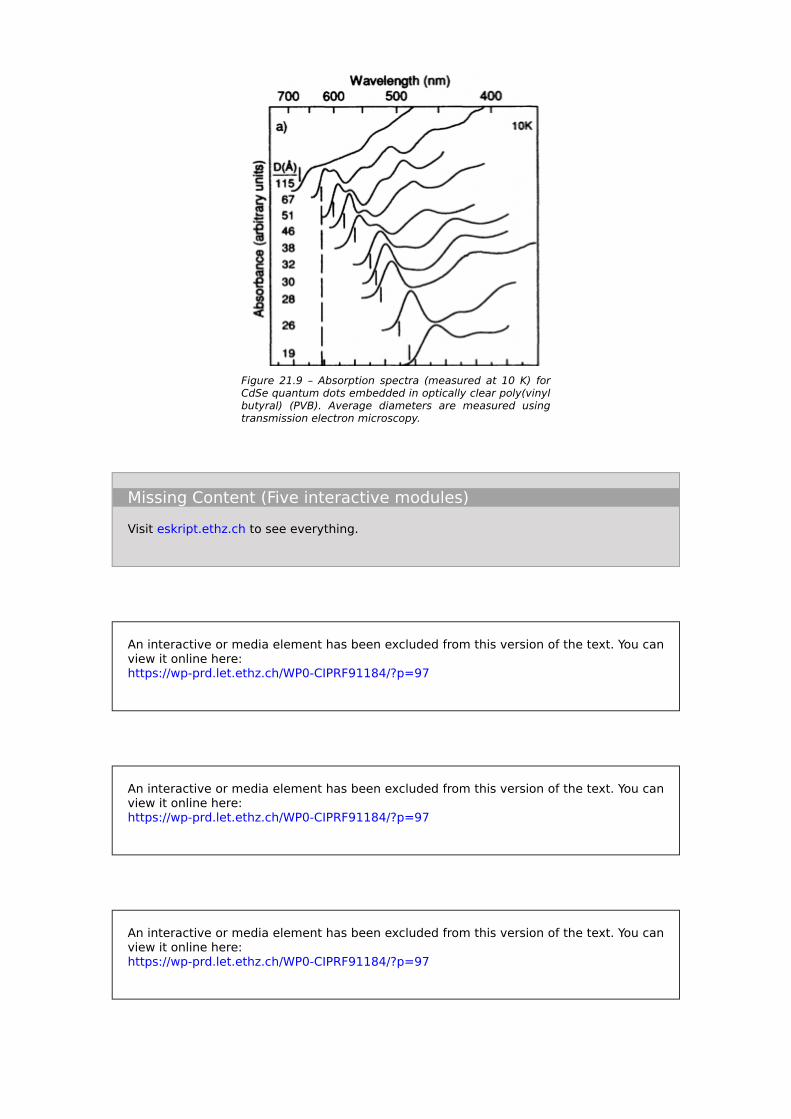
Figure 21.9 – Absorption spectra (measured at 10 K) for CdSe quantum dots embedded in optically clear poly(vinyl butyral) (PVB). Average diameters are measured using transmission electron microscopy.
Missing Content (Five interactive modules) Visit eskript.ethz.ch to see everything.
An interactive or media element has been excluded from this version of the text. You can view it online here: https://wp-prd.let.ethz.ch/WP0-CIPRF91184/?p=97
An interactive or media element has been excluded from this version of the text. You can view it online here: https://wp-prd.let.ethz.ch/WP0-CIPRF91184/?p=97
An interactive or media element has been excluded from this version of the text. You can view it online here: https://wp-prd.let.ethz.ch/WP0-CIPRF91184/?p=97

An interactive or media element has been excluded from this version of the text. You can view it online here: https://wp-prd.let.ethz.ch/WP0-CIPRF91184/?p=97
An interactive or media element has been excluded from this version of the text. You can view it online here: https://wp-prd.let.ethz.ch/WP0-CIPRF91184/?p=97

22
Band structures of some insulating materials
In this Chapter we will look at two examples of LCAO band structures of insulators in order to point out different features and their relationship with the properties.
22.1 – ReO3
ReO3 adopts a perovskite-like crystal structure in which the Re atoms are octahedrally coordi-nated by oxygens, but the A sites are vacant.
Figure 22.1 – ReO3 crystal structure showing the Re octa-hedrally coordinated with O and the vacant A site in the perovskite structure.
The electronic structures of Re and O are Re: [Xe] (4f)14(6s)2(5d)5
O: (1s)2(2s)2(2p)4
and in the extreme ionic limit the electronic structures of the Re6+ and O2- ions are Re6+: [Xe] (4f)14(5d)1
O2-: (1s)2(2s)2(2p)6 (Note that this extreme ionic limit is not very realistic but is helpful in interpreting the band
structure). The ionic picture suggests that the valence band should be made up primarily of oxygen 2p states, and the conduction band of Re 5d states. Importantly the conduction band will be partially filled with one electron per formula unit, the (5d)1 electron of Re6+. Indeed we see this in the band structure and density of states below:

Figure 22.2 – Calculated band structure and density of states for ReO3 . The Fermi level lies in the Re5d band. The horizontal dashed line indicates the position of the Fermi energy.
Let’s analyze some of the features of the band structure.
22.1.1 – Crystal field splitting A prominent feature of the band structure is the splitting of the Re 5d-derived conduction band into two sub-manifolds; this is particularly clear at the Gamma point. We call this splitting the crystal field splitting since its cause is the electrostatic interaction / coulomb repulsion between the electrons in the Re 5d orbitals and the surrounding oxygen 2p electrons which form the “crystal field”.
Figure 22.3 – d-orbitals energy levels in a free atom (left) and in the presence of an octahedral crystal field (right).
The Re orbitals that point directly towards a neighboring negative oxygen anion feel the most unfavorable coulomb interaction and so are raised the highest in energy. In the case of an octahedral crystal field, these are the dz2 and dx2-y2. The dxy, dyz and dxz orbitals experi-ence less Coulomb repulsion than the dz2 and dx2-y2 and so their energy is increased less; the convention is to leave the average energy unchanged from that of the free atom in the ener-gy-level diagram, so they appear to lower their energy.
The orbitals are often labelled by their group theoretical symmetries, with the lower energy threefold manifold called t2g and the higher energy twofold manifold eg. “t” and “e” indicate triple and double degeneracy, and “g” indicates symmetric (gerade) with respect to inversion.
Other examples of common crystal field splittings include square planar and the tetrahedral field splitting sketched below. The Cu ions in the high temperature superconducting cuprates experience a square planar crystal field, and the cations in zincblende semiconductors a tetra-hedral.
The following interactive module shows the energy diagrams for different crystal fields. You should drag the different geometries to their corresponding crystal fields.

Missing Content Visit eskript.ethz.ch to see everything.
An interactive or media element has been excluded from this version of the text. You can view it online here: https://wp-prd.let.ethz.ch/WP0-CIPRF91184/?p=109
22.1.2 – Flat Γ→Χ-Bands Another noticeable feature is the very flat dispersion of the Re d bands along the high symme-try line from to . We can understand this by looking at the LCAOs at both high symmetry points. Remember that, although we call the conduction band the Re 5d band, in fact it has partial O 2p character and is made up of the anti bonding Re 5d – O 2p combinations. Let’s sketch these combinations at k=0 and k=pi/a, first taking the t2g orbitals and the O 2p orbitals pointing along the bond direction as an example:
Figure 22.4 – The flat bands seen in the band structure of ReO3 are explained when looking at the linear combina-tions of orbitals at Γ and Χ: there is no bonding or antibond-ing interaction between the orbitals in both cases.
We see that there is no net bonding or anti bonding character at either the or point! The band, which we refer to as a “non-bonding” band, is flat, and has an energy close to that of the isolated Re 5d orbital, influenced of course by the electrostatic crystal field. One could make a similar combination with the eg orbitals to account for the flat band at higher energy, and with bonding intra-unit cell combinations to explain the flat regions in the valence band.
22.1.3 – Understanding the band curvature Let’s look at the LC of a t2g orbital with an O p orbital that is perpendicular to the bond direction. We’ll take the example of the valence band in which there are bonding interactions between the Re d and the O p orbitals within the unit cell and the oxygen character is domi-nant. At k=0 we find that the interactions between unit cells are anti-bonding:

Figure 22.5 – Combination of Re5d and O2p orbitals show-ing bonding character within the unit cell and anti-bonding character between the unit cells.
For we have bonding interactions within and between the unit cells and therefore the energy is lowered relative to the combination.
Figure 22.6 – Re5d and O2p showing bonding character within and between the unit cells.
We understand, therefore, why the O2p bands curve downwards from Gamma to X. If we made the analogous sketches for the antibonding intra-unit cell combinations, corresponding to the conduction band, we would be able to justify the opposite curvature seen in the band structure.
22.2 – AgCl and KCl
Figure 22.7 – Band structure for KCl. Note the narrow bands for KCl indicating the very ionic character.

Figure 22.10 – Nearest neighbor vectors.
Figure 22.8 – Band structure of AgCl.
22.3 – Graphene Graphene is a two dimensional single atomic layer of carbon atoms arranged in a honeycomb lattice.
Figure 22.9 – Graphene structure with primitive cell.
There are two carbon atoms per primitive cell, A and B, shown in blue and red colors, respec-tively.
Carbon atoms present the following electronic configuration: 1s2 2s2 2p2, with the 4 valence electrons in the second shell. All C atoms are sp2 hybridized (one 2s orbital together with the 2px and the 2py orbitals generate three sp2 orbitals). These sp2 orbitals form strong covalent in plane σ-bonds with the sp2 orbitals of neighboring C atoms. As the bonding orbital associat-ed with each σ-bond is occupied by two electrons (spin up and spin down), there is one electron per C atom left in the 2pz orbital. The 2pz orbitals stick out of the plane and form π-bonds with neigboring 2pz orbitals.
Using the Linear Combination of Atomic Orbitals (LCAO) we can derive the band structure for the π orbitals. To do so, the nearest neighbor vectors, \vec{n_{1}}, \vec{n_{2}}, \vec{n_{3}} (see next fig-ure) will be useful for writing the final solution in a compact form:

The corresponding energies can be obtained by solving the following determinant:
where is the energy of the pz orbital, , with
the pz orbital on atom 1 and the pz orbital on atom 2. is the term accounting for the interaction with the nearest neighbors, and corresponds
to
The solutions are . Let’s plot them:
Figure 22.11 – (Left) Definition of Gamma, K and M points. **NOTE THAT THERE IS A MISTAKE IN THE FIGURE. THE K POINT IS AT (0, 4pi / 3a) AND THE M POINT IS AT (2pi / sqrt(3)a, 0)** (Right) LCAO band structure of graphene.
Some comments regarding the band structure: • Ep has been chosen to be equal to 0 eV. • As there is 1 electron per orbital, the band is half filled, so the Fermi energy lies in the
middle (E=0 eV). • The bandwidth is equal to 2 times the number of nearest neighboring atoms
. • Near the Γ points, the energy is like for a normal free electron. • The behavior is insulating except in the K points, where the energy is linear in k. This
feature in the band structure is called a Dirac Cone, and so the electrons are called Dirac Fermions. Such a linear relation is found as the solution to the Dirac equation in

the limit of zero electron mass, so the Fermi velocity is
the analogue to the speed of light for electrons.
Interactive module. Match the octahedrally coordinated transition metal ions with their correct electronic
arrangement in the squares below.
Missing Content Visit eskript.ethz.ch to see everything.
An interactive or media element has been excluded from this version of the text. You can view it online here: https://wp-prd.let.ethz.ch/WP0-CIPRF91184/?p=109

23
Coupling with structure
23.1 – Peierl’s Distortions Let’s work out the band structure of a one dimensional chain with two atoms per unit cell. First we remind ourselves of the simple one atom per unit cell case:
Figure 23.1 – 1D chain with 1 atom per unit cell.
which has the dispersion we derived previously
Figure 23.2 – Dispersion relation of a 1D chain with 1 atom per unit cell. The range of k values is from [latex] -\pi/ a[/latex] to [latex]+\pi/a[/latex]
If each atom contributes one electron to the band, then is half way up the band, since the total band can take 2 electrons per atom. In the exercises you worked out what happens when you double the size of the unit cell so that each contains two atoms as sketched below:
Figure 23.3 – 1D chain with 2 identical atoms per unit cell.
If the atoms are identical of course the result must be the same as the one atom per unit cell case, but let’s remind ourselves anyway. We proceed by making bonding (B) and anti-bonding (AB) combinations of the atoms within the unit cell, then see how they interact at and
at the Brillouin zone boundary (which is now at ).

We see that the two intermediate energy states at are equal in energy. By inspec-
tion we can sketch the bandstructure, which is shown by the thick red in line in the following figure. The dashed red line is our original result for one atom in the unit cell, and it is equiva-lent to the solid red line because of the periodicity of the chain which tells us that any k-point,
is equivalent to .
Figure 23.5 – Bandstructure for the linear chain (red) and a dimerized (blue) chain having 2 atoms per unit cell.
Again is halfway up the band as expected. Now let’s dimerize the chain
Figure 23.6 – Dimerized 1D chain with 2 atoms per unit cell.
Now the two intermediate energy combinations at are not degenerate! The intra-unit cell bonding wave functions have stronger bonding and weaker anti-bonding interac-tions than the intra-unit cell anti-bonding combinations! As a result the band structure of the dimerised chain has a band gap at . Since all of the energy levels up to the gap are filled, the dimerised material is an insulator.

We can see, also, that the energy levels that are filled with electrons have moved to lower energy and so the total electronic energy of the chain has been lowered by the distortion. (The states that moved up to higher energy in this example were empty). Peierl’s theorem tells us the conditions for which this lowering of electronic energy is strong enough to cause such a dimerization of the crystal lattice:
Peierl’s Theorem
A one-dimensional metal is always unstable with respect to a structural distortion that lifts the degeneracy at the Fermi level.
In the case shown above the distortion has a repeat unit of length . In
fact this result is general: the period of the superlattice period, that is the size of the new unit cell, is half the wave length of the highest filled energy level, that is divided by theFermi
wave vector .
An example: Polyacetylene, which consists of polymerized acetylyene/ethylene C2H2
Figure 23.8 – A sphere-rod model illustration of a polyacetylene chain.
Each carbon atom uses three of its valence electrons forming strong covalent sp2 hybrid bonds with the two neighboring carbon atoms and a hydrogen. Since C has four valence electrons, each C atom has an additional valence electron available, which occupies a p-orbital perpen-dicular to the chain. These p electrons interact through pi bonding, and so their LCAO band structure has a similar dispersion to that of a chain of s orbitals.
Figure 23.9 – Bonding and anti bonding LCAOs for the out-of-plane p orbitals.

Figure 23.10 – Bandstructure of the out-of-plane p orbitals.
is at so at first sight we would expect polyacetylene to be a metal. Peierl’s
theorem tells us, however, that a distortion with periodicity should occur,
which would open a gap and the system should be insulating. Indeed polyacetylene is an insulator with a band gap of 2 eV and the C-C bond length alter-
nates from 136 pm for the double bond to 144 pm for the single bond, an 8 pm difference which is around 6%.
Note that alternating single and double C-C bonds would have much larger bond length alter-nations (single bond: 1.52 Å and double bond: 1.34 Å. From David R. Lide, A survey of carbon-carbon bond lengths, Tetrahedron, Link).
23.2 – Jahn-Teller Distortion Next we illustrate another electronically driven structural distortion –the Jahn-Teller distortion– using perovskite structure LaMnO3 as an example.
Figure 23.11 – The perovskite structure of LaMnO3: The
oxygen atoms (O2-; [Ne]) are shown in red, the La atoms (La3+; [Xe]) are shown in blue and the central Mn atom (Mn3+; [Ar](3d)4) is shown in yellow.

Figure 23.12 – Mn 3d energy levels in a free atom (left), in an octahedral crystal field (middle) and after a Jahn-Teller distortion (right).
We saw earlier that the octahedral crystal field splits the Mn 3d orbitals into three t2g orbitals of lower energy and two eg orbitals of higher energy. The Mn3+ ion in LaMnO3 has four 3d elec-trons and it is not immediately obvious how to arrange them between the t2g and eg manifolds: Putting two electrons into the same orbital costs a coulomb repulsion (and we will see later also an exchange) energy, whereas putting the fourth electron into an eg level costs the crystal field splitting. In the case of [6]-coordinated Mn, the high-spin arrangement shown in the fig-ure above, in which the 4th 3d electron occupies an eg orbital, is lower in energy than low-spin arrangement with two electrons paired in a t2g level.
Now we see that the single eg electron has a choice of which of the two orbitals to occupy – the eg manifold is half-filled, similar to the case of the half-filled band we discussed for the Peierl’s distortion. In practice, a structural distortion occurs that lowers the energy of one of the two orbitals, which the electron then occupies, at the expense of raising the energy of the other; since the other orbital is empty this doesn’t cost any electronic energy. A typical Jahn-Teller structural distortion is shown in the lower right sketch: the Mn-O bonds along the z axis elongate, lowering the Coulomb repulsion of an electron in the dz2 (and dxz and dyz) orbitals, and the x-y plane bonds shorten, raising the energy of electrons in orbitals in the plane.
As in the Peierl’s distortion case, there is a competition between the strain energy cost and the electronic energy lowering. Such a splitting would not happen for a structure with 3 elec-trons in the d-orbitals, as there would be no electronic energy gain; in fact the rule for a Jahn-Teller to occur is that the electron must have a choice between equivalent energy orbitals (we call this an orbital degeneracy).
Missing Content: 5 interactive modules Visit eskript.ethz.ch to see everything.

An interactive or media element has been excluded from this version of the text. You can view it online here: https://wp-prd.let.ethz.ch/WP0-CIPRF91184/?p=122
An interactive or media element has been excluded from this version of the text. You can view it online here: https://wp-prd.let.ethz.ch/WP0-CIPRF91184/?p=122
An interactive or media element has been excluded from this version of the text. You can view it online here: https://wp-prd.let.ethz.ch/WP0-CIPRF91184/?p=122
An interactive or media element has been excluded from this version of the text. You can view it online here: https://wp-prd.let.ethz.ch/WP0-CIPRF91184/?p=122
An interactive or media element has been excluded from this version of the text. You can view it online here: https://wp-prd.let.ethz.ch/WP0-CIPRF91184/?p=122

24
Summary
An interactive or media element has been excluded from this version of the text. You can view it online here: https://wp-prd.let.ethz.ch/WP0-CIPRF91184/?p=123
Solution: Have a look after having first tried yourself above! • The properties of a material are strongly coupled to its band structure. It lets us
distinguish between metals (the Fermi energy lies within the band) and insulators or semiconductors (some bands are completely filled and others are completely empty).
• The conductivity of a metal is reflected in the band structure. Broad bands present a large ß, which is a sign of strongly overlapping orbitals, and therefore of good conductivity. Analogously, narrow bands are a sign of poor conductivity.
• The effective mass of an electron is inversely proportional to the curvature of the band. For large curvatures, the effective mass is small, and therefore conductivity is high.
• In some regions of the band structure the curvature of the band can be negative, and so the effective mass is also negative. Instead of considering a negative mass, we think of the current in these regions as being carried by positively charged holes having positive mass.
• In optical absorption, an incoming photon excites an electron from the valence band to the conduction band and is absorbed during the process, which requires the conservation of energy and momentum.
• In direct gap semiconductors, the k value of the electron is the same in its ground and excited states, and therefore the transition is vertical within the the band structure. On the other hand, in indirect gap semiconductors the transition takes place in 2 steps: the absorption of a photon is followed by the emission or absorption of a phonon, allowing for the conservation of momentum.
• The transition probability amplitude (TPA) is the probability of an electron in a particular valence band to make the transition into a particular conduction band state.
• The transition probability amplitude can be evaluated using symmetry arguments. As the transition operator presents odd parity, the probability will only be different from zero (and therefore the transition possible) when the initial and the final states have different parity, such as between an s orbital (even parity) and a p orbital (odd parity).
• In summary, optical transitions must conserve energy, momentum and parity. • In semiconductor quantum dots, the bandgap depends on the size: as the size
decreases, the bandgap becomes larger. • An exciton is an electron-hole pair bound by a Coulomb interaction, with a binding
energy inversely proportional to the relative permittivity. • According to the Peierl’s theorem, a one-dimensional metal is always unstable with
respect to a structural distortion that removes a degeneracy at the Fermi level, with a periodicity equal to π over the k at the Fermi level. It consists of a balance between the strain energy cost and electronic energy lowering.
• Crystal field splitting is a consequence of the coupling between the electronic structure and the physical structure. For example, in the case of d orbitals, depending on the coordination (tetrahedral, octahedral…) the energy of some orbitals is raised and that of others is lowered.
• The Jahn-Teller distortion is an electronically-driven structural distortion, which consists of the elongation along an axis and a shortening along the other two axes. It will take place when the saving in electronic energy is higher than the cost in strain energy.


V
Magnetism
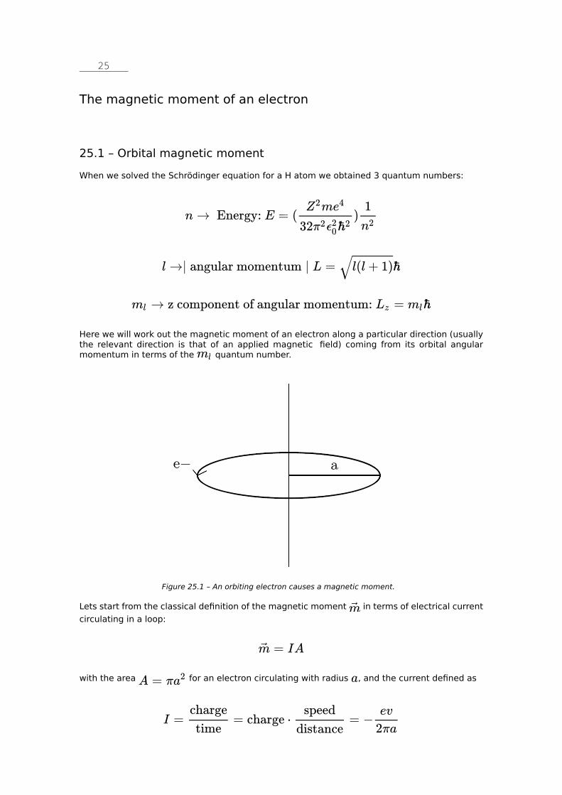
25
The magnetic moment of an electron
25.1 – Orbital magnetic moment When we solved the Schrödinger equation for a H atom we obtained 3 quantum numbers:
Here we will work out the magnetic moment of an electron along a particular direction (usually the relevant direction is that of an applied magnetic field) coming from its orbital angular momentum in terms of the quantum number.
Figure 25.1 – An orbiting electron causes a magnetic moment.
Lets start from the classical definition of the magnetic moment in terms of electrical current circulating in a loop:
with the area for an electron circulating with radius , and the current defined as

The magnetic moment is then given by
We know in addition from classical mechanics that the angular momentum around an axis in general is , and from quantum mechanics, the angular momen-tum of an e in an atom is given by , so we can use
Substituting this expression for in the previous expression for we obtain the following expression for the magnetic moment along the circulation axis:
Here is called the Bohr magneton. So we see that the
quantum number determines the orbital magnetic moment of an e– as well as its angular momentum.
Notice that this is the only contribution to the magnetism of an electron that we obtain from solving the Schrödinger equation.
25.2 – Electron Spin We know that electrons also have a spin contribution to their magnetic moment in spite of the fact that this does not appear in the solution to the Schrödinger equation. In fact if were were to solve the relativistic Dirac equation, which is a relativistic extension to the Schrödinger equa-tion, we would obtain two additional quantum numbers describing the electron spin. These are , which is analogous to the quantum number except that it always takes the value 1/2, and
and , which takes the values -s, -s+1, … s-1, s, that is and is analogous to .
By analogy with and , the quantum number gives us the total spin angular momentum according to the expression:
and gives us the component of the spin angular momentum along an axis
.
But when we convert the angular momentum into the magnetic moment, we have to be a bit careful because the analogy is not exact. In fact the magnetic moment along a particular direction/axis is given by

(rather than just which would be analogous to the we obtained for the orbital component). For an electron spin, it turns out conveniently that and so the magnetic moment along a chosen direction is .
Notice the minus sign: If ; if .
The total magnetic moment is obtained by vector addition of spin and orbital components; this is a bit complicated but fortunately tables exist to help with this (they are called the Cleb-sch-Gordon coefficients). In many of the materials that we are interested in, only the spin part is important for determining the magnetic properties and so for most of this class we will ignore the contribution to from orbital angular momentum and take the magnetic moment of the electron to be .

26
Magnetic moments in atoms
We have seen that each electron has an orbital magnetic moment and a spin magnetic moment . In this section we will look at how these magnetic moments combine in an atom to give an overall atomic magnetic moment (or not).
26.1 – The He atom We’ll begin by working out when it is energetically favorable for electrons to have their spins parallel (so that their moments add) or anti-parallel (so that they cancel). We will take the sim-plest possible example of the He atom which has only two electrons, both of which are in s orbitals so that and they each have only a spin magnetic moment.
First we remind ourselves that in the ground state, where both of the electrons occupy the 1s atomic orbital, they are required to have opposite spins. We learned this as the Pauli principle in our introductory chemistry classes — no two electrons can have the same value for all of their quantum numbers, so that if they occupy the same atomic orbital (and hence have the same values for , and ) their spins must be opposite so that they have different values for . Therefore a He atom in its ground state does not have a magnetic moment.
Next we want to compare two possibilities for the first excited state, in which one electron is in the 1s orbital and one in the 2s. Now the electrons are allowed to have their spins parallel because their quantum numbers are different, or of course they can still keep the anti-par-allel configuration. We will work out which of these two combinations has the lowest energy, bearing in mind that both are very likely to have a higher energy than the ground sate.
Figure 26.1 – Possible spin configurations for the He atom.
We write the Hamiltonian for the He atom as the sum of the Hamiltonian for electron 1 in the absence of electron 2, , plus the Hamiltonian for electron 2 if electron 1 were not there,
, plus the interaction between the electrons, :
Here is the position of the electron 1, and the position of electron 2. Notice that the Hamiltonian depends only on the position of the electrons, not on their spin, and so the two spin configurations of the excited state can only have different energies if the spin affects the spatial distribution of the electrons. In fact it does, and to see why we have to use a more rig-orous statement of the Pauli Principle, as follows:

Formal definition of the Pauli Principle
The total electronic wavefunction must be antisymmetric with respect to the inter-change of two electrons.
(This is a particularly good thing to know for conversation at aperos.) In general the wavefunction is made up of the product of the usual spatial part, that
we have been dealing with so far, times a part describing the spin of the electrons which we will call . The Pauli principle tells us that, if we write the two-electron wavefunction as
, when we switch the electrons, so that electron 1 takes the place of electron 2 and vice versa, the wavefunction must change sign. That is
If the two electrons have the same spin, then the spin part of the wavefunction is symmetric and doesn’t change sign when we switch the two electrons, i.e. . In this case the spatial part has to be antisymmetric to satisfy the Pauli principle, i.e.
. If the two electrons have opposite spin, however, the spin part of the wavefunction changes sign when the electrons are interchanged and the spatial part must be symmetric to satisfy the Pauli principle.
It’s beyond the scope of this course to derive explicit forms for the spatial part of the two-electron wave functions that have the appropriate symmetry properties, and we will just make use of the answer:
Symmetric spatial:
Antisymmetric spatial:
Here represents electron 1 in the 1s orbital, electron 1 in the 2s orbital, electron 2 in the 1s orbital and electron 2 in the 2s orbital. You should
check for yourself that when you switch and , the symmetric wavefunction is unchanged, whereas the anti-symmetric wavefunction changes its sign.
The allowed combinations are summarized in the table below.
Now we calculate the expectation values of the energy for these two spatial wave functions,
remembering that the symmetric spatial wavefunction corresponds to oppositely oriented spins with no net magnetism, and the antisymmetric wavefunction to the parallel spins and a net magnetic atom. Since we will have a lot of integrals to write out we’ll use the bra-ket notation that we intro-duced earlier:

Then the energies of the two two-electron wave functions are given by:
We see that the wavefunction with the + sign, corresponding to the anti-parallel spins has energy and the wavefunction with the – sign, for which the spins are parallel has energy . Since is a positive integral, this means that the energy is lower by an amount when the spins are parallel than when they are antiparallel, and the first excited state of He is magnetic! Let’s look at the different terms in the total energy and see what they correspond to physically:
is the energy of electron 1 or electron 2 in the 1s orbital, and
is the energy of electron 1 or electron 2 in the 2s orbital. These are the values that we would obtain if we solved the Schrödinger equation for a He nucleus but just one electron (i.e. the He+ ion).
and are the terms that account for the explicit many body electron-electron interac-tions. is the Coulomb repulsion between the two electrons, which we can easily see by rear-ranging the expression:
Here we have written is the charge density of electron 1 in the 1s orbital, and likewise for electron 2 in the 2s orbital. This is exactly the expression for a Coulomb interaction between two electrons.
doesn’t have such a classical analogue. We call it the exchange interaction since the left and right hand sides of the expression are obtained from exchanging electrons 1 and 2 between their orbitals:

In fact it would be zero except for the requirement that the electrons obey the Pauli Principle and the wavefunction be antisymmetric!
To summarize, then, the ground state of He is non-magnetic because the two electrons must have opposite spins in order to both occupy the lowest energy atomic orbital. In the first excit-ed state, in which one electron occupies the 2s orbital, the magnetic arrangement is lower energy than the non-magnetic. But both arrangements are higher in energy than the ground state.
26.2 – How can an atom have a magnetic ground state? We saw that in the case of He the ground state is non-magnetic because of the requirements of the Pauli principle. There are situations, however, in which the ground state of atoms (or ions or molecules) can be magnetic:
1. If there are an odd number of electrons, in an atom or ion, then one of them must always be unpaired. An example would be the Ni3+ ion, which has 7 d electrons, in an octahedral crystal field. Here the low-spin arrangement shown below right is usually lowest in energy and has a spin magnetic moment of . The high spin arrangement, below left, is also magnetic with a spin moment.
2. If there are degenerate orbitals e.g. in the O2 molecule
3. i.e. \Delta E" title="2J> \Delta E" class="latex mathjax">. When the exchange energy is larger than the energy difference between the ground and excited states. We’ll see next that this is often the case for 3d electrons in transition metals and their compounds but usually not the case for s or p electrons.
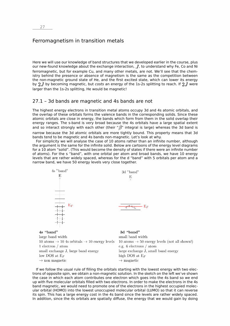
27
Ferromagnetism in transition metals
Here we will use our knowledge of band structures that we developed earlier in the course, plus our new-found knowledge about the exchange interaction, , to understand why Fe, Co and Ni ferromagnetic, but for example Cu, and many other metals, are not. We’ll see that the chem-istry behind the presence or absence of magnetism is the same as the competition between the non-magnetic ground state of He, and the first excited state, which can lower its energy by by becoming magnetic, but costs an energy of the 1s-2s splitting to reach. If were larger than the 1s-2s splitting, He would be magnetic!
27.1 – 3d bands are magnetic and 4s bands are not The highest energy electrons in transition metal atoms occupy 3d and 4s atomic orbitals, and the overlap of these orbitals forms the valence bands in the corresponding solids. Since these atomic orbitals are close in energy, the bands which form from them in the solid overlap their energy ranges. The s-band is very broad because the 4s orbitals have a large spatial extent and so interact strongly with each other (their “ ” integral is large) whereas the 3d band is narrow because the 3d atomic orbitals are more tightly bound. This property means that 3d bands tend to be magnetic and 4s bands non-magnetic. Let’s look at why.
For simplicity we will analyse the case of 10 atoms rather than an infinite number, although the argument is the same for the infinite solid. Below are cartoons of the energy level diagrams for a 10 atom “solid”. (This would become the density of states if there were an infinite number of atoms). For the s “band”, with one orbital per atom and broad bands, we have 10 energy levels that are rather widely spaced, whereas for the d “band” with 5 orbitals per atom and a narrow band, we have 50 energy levels very close together.
If we follow the usual rule of filling the orbitals starting with the lowest energy with two elec-trons of opposite spin, we obtain a non-magnetic solution. In the sketch on the left we’ve shown the case in which each atom contributes one electron which goes into the 4s band so we end up with five molecular orbitals filled with two electrons. In order to make the electrons in the 4s band magnetic, we would need to promote one of the electrons in the highest occupied molec-ular orbital (HOMO) into the lowest unoccupied molecular orbital (LUMO) so that it can reverse its spin. This has a large energy cost in the 4s band since the levels are rather widely spaced. In addition, since the 4s orbitals are spatially diffuse, the energy that we would gain by doing

this, given by the integral, turns out to be quite small. In the 3d band, in contrast, the spac-ing between the HOMO and LUMO is tiny, and so there is very little energy cost to moving an electron up into an empty band. In addition, the more tightly bound 3d electrons have larger
integrals. As a result, the balance is that 4s bands remain non-magnetic, whereas 3d bands become magnetic. An approximate criterion for magnetism in solids is that the exchange inte-gral should be larger than around 1/5 of the bandwidth.
The density of states of the transition metals is usually drawn with the exchange interaction accounted for, so that the states for one spin direction are lower in energy than for the other spin direction in the 3d band. We illustrate this below, and indicate the positions of the Fermi level for some example transition metals.
Figure 27.2 – Band structure of transition metals indicating the energy difference between up- and down-spin d bands caused by the exchange interaction.
27.2 – Magnetism and the position of the Fermi level in transition metals Armed with this knowledge about the competition between exchange and band width we can now understand the trends in magnetic properties across the transition metal series. We will use two additional pieces of physics: First, the band structure and density of states is very sim-ilar across the 3d transition metals, and all that varies as we move from one element to the next is the position of the Fermi level. This is called the rigid band model. Second, that the valence electrons from the atoms fill up the valence bands in the solid without regard to what their original atomic orbital character was.
The electronic structure of a Cu atom is [Ar] (3d)10(4s)1. In solid Cu, there are sufficient valence electrons (11 per atom) that the entire 3d band is filled up and the Fermi energy lies in the non-spin-polarised 4s band. Therefore Cu is not magnetic. It is also, as we pointed out earlier, a good conductor, since the 4s electrons at the Fermi energy have low effective mass and high mobility.
In Fe, Co and Ni –the three elemental ferromagnetic transition metals– the Fermi energy lies within the spin-polarized 3d band which explains why these metals are ferromagnetic.
For Cr and Mn, the Fermi energy also lies within the 3d band and so we might expect them also to be ferromagnetic. In fact they are indeed locally magnetic, but the magnetism varies periodically throughout the solid giving no overall magnetization. We call this antiferromagnet-ism, and will return to its origin in the next section.

28
Magnetoresistance
The term magnetoresistance, often written as MR, refers to the change in electrical resistivity of a material or system when a magnetic field is applied. The formal definition is
Magnetoresistance, MR
where is the resistance in the presence of the field,and the resistance with no field applied. Sometimes it is also expressed as a percentage obtained by multiplying this value by 100, but this can look rather silly as the resulting number can be greater than 100.
All metals have a magnetoresistance because the magnetic field changes the pathway by which the electrons travel through the solid (we can understand this at the simple level of the Hall effect). Usually, however, the effect is quite small. Here we will discuss how, by cleverly arranging different metals in a multilayer structure, a large, technologically relevant magne-toresistance can be engineered. This is called giant magnetoresistance. Peter Grünberg and Albert Fert were awarded the 2007 Nobel Prize, and Stuart Parkin the 2014 Millennium Tech-nology Prize for the fundamental discovery and technological development of the giant mag-netoresistance phenomenon.
28.1 – Giant magnetoresistance Giant magnetoresistance is based on the phenomenon of interlayer exchange coupling. When two layers of ferromagnetic metal such as iron are separated by a non-magnetic or antiferro-magnetic metal such as Cr, the orientation of the magnetization in the second layer depends on its distance from the first.
Figure 28.1 – The geometry of a multilayer for measuring interlayer exchange coupling.
Here is the original data from Peter Grünberg’s lab book that he showed in his 2007 Nobel prize lecture:
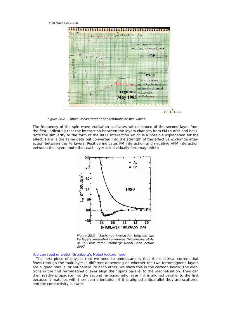
Figure 28.2 – Optical measurement of excitations of spin waves.
The frequency of the spin wave excitation oscillates with distance of the second layer from the first, indicating that the interaction between the layers changes from FM to AFM and back. Note the similarity to the form of the RKKY interaction which is a possible explanation for the effect. Here is the same data but converted into the strength of the effective exchange inter-action between the Fe layers. Positive indicates FM interaction and negative AFM interaction between the layers (note that each layer is individually ferromagnetic!):
Figure 28.3 – Exchange interaction between two Fe layers separated by various thicknesses of Au or Cr. From Peter Grünbergs Nobel Prize lecture 2007.
You can read or watch Grunberg’s Nobel lecture here The next piece of physics that we need to understand is that the electrical current that
flows through the multilayer is different depending on whether the two ferromagnetic layers are aligned parallel or antiparallel to each other. We show this in the cartoon below: The elec-trons in the first ferromagnetic layer align their spins parallel to the magnetisation. They can then readily propagate into the second ferromagnetic layer if it is aligned parallel to the first because it matches with their spin orientation; if it is aligned antiparallel they are scattered and the conductivity is lower.

To be a bit more rigorous, we can look at the separate up- and down- spin densities of states, in particular in the region of the Fermi energy. In the first ferromagnetic layer in the picture below, there are many states available at the Fermi level for electrons of up-spin, but very few for down-spin electrons, and so mostly only up-spin electrons make it through the first ferro-magnetic layer and into the non-magnetic layer. In the non-magnetic layer, states are available at the Fermi energy for electrons of either spin. If the second ferromagnetic layer has its mag-netisation parallel to the first, then there are again many up-spin states at the Fermi energy, and the electrons are able to continue conducting.
Figure 28.5 – DOS of the layers of a FM / non-magnetic / FM multilayer in its low resistance state with the magnetic layers aligned parallel.
If the second ferromagnetic layer is aligned antiparallel to the first, then its available states at the Fermi energy are of the opposite spin type than the incoming electrons as sketched below. The resistance is high because there are few states available for the incoming electrons which are therefore unable to propagate and instead scatter.
Figure 28.6 – DOS of the layers of a FM / non-magnetic /FM multilayer in its high resistance state with the magnetic layers aligned antiparallel.
In the extreme case when there are states of only one spin type at the Fermi energy, the cur-rent is 100 % spin polarized. Such a material is called a half-metallic ferromagnet. In this case the antiparallel arrangement of the magnetisation in the layers has the highest possible resis-tance.

This giant magnetoresistive device is often called a “spin valve”. It can be used as a magnetic sensor by fixing the first ferromagnetic layer and letting the second layer respond to an exter-nal field. This is often used in the read heads of hard disk drives as sketched below.
Figure 28.7 – Schematic of a giant magnetoresistive spin valve in a magnetic read head. The orientation of one FM layer is fixed, and the other reorients parallel to the external magnetic field from a magnetic data bit. A current is passed through the device to detect whether the FM layers are aligned parallel (low resistance) or anti-parallel (high resistance).
In the next section we will look at a particularly interesting piece of physics — called exchange bias coupling – which allows us to fix the orientation of a FM layer.
An interactive or media element has been excluded from this version of the text. You can view it online here: https://wp-prd.let.ethz.ch/WP0-CIPRF91184/?p=146
28.2 – Exchange Bias Coupling When a layer of a ferromagnetic material is adjacent to a layer of an antiferromagnet, the anti-ferromagnet often pins the orientation of the magnetisation in the ferromagnet. We can under-stand this at least qualitatively in the cartoon below: the first layer of Fe atoms in the AFM couples ferromagnetically to the first layer in the FM causing the Fe moments to be oriented preferentially to the right in this case. When an external field is applied to the left, the FM Fe tries to reorient parallel to the field, but this upsets the spins at the interface to the AFM, which does not respond to the applied magnetic field. Therefore the Fe layer remains pinned with its magnetisation oriented to the right.
An interactive or media element has been excluded from this version of the text. You can view it online here: https://wp-prd.let.ethz.ch/WP0-CIPRF91184/?p=146

Figure 28.8 – Exchange biased hysteresis loop.
In fact this simple cartoon does not tell the whole story. For example it would predict no exchange bias for the arrangement shown below, when in fact one can also exist. The detailed mechanism for exchange bias is in fact not yet understood and is an active area of research.
28.3 – Colossal Magnetoresistance in doped LaMnO3
After giant magnetoresistance, researchers were running out of adjectives to describe large change in resistivity with magnetic field. Therefore when a magnetic field was found to cause a transition from a metallic to an insulating state in a family of perovskite-structure transition metal oxides, the term “colossal magnetoresistance” was used. In (La,Ca)MnO3 and related materials a huge change of resistance from an insulating to a metallic state is caused by appli-cation of a magnetic field. The original data is shown below. Unlike Giant Magnetoresistance, widespread device applications have not been identified due to the high fields (of the order of a few teslas) needed.

Figure 28.10 – Resistance as a function of applied magnetic field in a (La,Ca)MnO3 perovskite film at 77K. At zero field the material is an insulator, and it becomes metallic in the (rather large) field of 2T.
In the next Chapter we will discuss the physics and chemistry of the transition metal oxides, so that we can understand this colossal magnetoresistance phenomenon.
An interactive or media element has been excluded from this version of the text. You can view it online here: https://wp-prd.let.ethz.ch/WP0-CIPRF91184/?p=146

29
Antiferromagnetism in transition metals
Here we will look at two mechanisms by which the exchange interaction, which by definition favours ferromagnetic alignment of electrons, can in fact lead to an overall anti-ferromagnet-ism in metallic systems.
29.1 – Spin spirals from Fermi surface nesting We’ll begin with the case of metallic Cr which is antiferromagnetic with a magnetic spiral struc-ture who’s wavelength is close to but not exactly matching the spacing between atoms. We call this an incommensurate spin spiral.
Figure 29.1 – (a) Commensurate spin-density wave. (b) Incommensurate spin-density wave.
The physics behind the spin spiral is actually conceptually similar to that causing the Peierls distortion. Remember in the 1D chain of atoms spaced by a distance , doubling the unit cell by moving pairs of atoms closer together opened a gap half way through the Brillouin zone. We argued that, if the band were half-filled, this process would happen spontaneously since the gap opening would lower the energy of the occupied orbitals, and the orbitals that would be raised in energy would anyway be empty.
There are other ways of opening a gap halfway through the Brillouin zone apart from dimeris-ing the atoms. One that we already looked at is to make alternate atoms be different, by form-ing an A-B-A-B… chain. We looked specifically at the example of alternating s and p orbitals. Another possibility, and the one that is relevant here, is to alternate the spin directions in an antiferromagnetic pattern:
In this case the lower energy state at one k-point at the band gap (
say) has larger amplitude on the atoms of one spin orientation (up-spin say) and the higher energy state has larger amplitude on the atoms of the opposite orientation (down-spin). At the other previously equivalent k-point, , the lower energy state has larger
amplitude on the down-spin atoms and the higher energy on the up-spin atoms.

Remember that for the Peierls distortion, we also saw that, in the general case, if the Fermi
wave vector is , the periodic lattice distortion would have wavelength rather than
. In the case of the formation of antiferromagnetism, a general Fermi wavevector leads to a periodic spin wave that doesn’t match the underlying lattice.
Cr, of course, is not a 1-dimensional chain but is made up of a 3-dimensional lattice of atoms with a 3-dimensional Fermi surface in reciprocal space. In this case it is generally not possi-ble to find a structural distortion or magnetic spin wave with a periodicity that will open a gap across the entire Fermi surface, and remember that it is the gap opening that drives the process by making it energy lowering. Sometimes, however, the detailed structure of the Fermi surface results in large fractions of reciprocal space in which different regions of the Fermi sur-face are parallel. This occurs in Cr which has an electron pocket near the Brillouin Zone centre and a hole pocket near the corners:
Figure 29.3 – An (001) cross-section through the body-centered cubic Brillouin zone, showing the Fermi surface of Cr. From W. A. Harrison, Electronic Structure and the properties of solids. Dover 1989.
Large regions of these pockets are parallel to each other, and therefore separated by the same
wave vector . In this case a spin wave with periodicity given by opens a partial gap
at the Fermi level which is sufficient to lower the energy and therefore happens spontaneous-
ly. For Cr , which is very close to the distance from the centre of the Brillouin
Zone to the Zone boundary (the H point in the figure above is the point (0,0,1)). If this so-
called “nesting” vector were exactly , Cr would show commensurate AFM ordering with
the body-centred and corner atoms anti-aligned to each other. Instead, it has a spin density wave with a repeat wavelength of around 10 unit cells, determined by the deviation of the
value from .

29.2 – The RKKY interaction If one solves the Schrödinger equation for a point magnetic moment introduced in a free-elec-tron gas, one finds that, as expected, the electrons around the magnetic moment align their spins parallel to the magnetic moment so as to optimise their exchange interaction. The mag-netisation density then oscillates, so that further away from the moment there are regions where the spins of the free-electron gas are antiparallel to the introduced moment. The actual functional form is plotted below (note that the apparent discontinuities are just changes in the vertical scale, since the magnitude of the spin polarisation drops off quickly).
Figure 29.4 – Magnetization of free electrons around a point magnetic moment placed at the origin, according to RKKY the-ory. The horizontal axis is 2kFr, where kF is the Fermi wave vector. The vertical axis is proportional to the magnetization induced by a point source at r=0.
This is called the RKKY interaction after the scientists (Ruderman, Kittel, Kasuya and Yosida) who first proposed it.

30
Magnetism in Transition Metal Oxides
In this section we will first review the factors that determine the sizes of the local magnetic moments on transition metal ions in oxides, and then discuss how the chemical bonding between the transition metal and the oxygen determines the relative arrangement (ferromag-netic, antiferromagnetic, etc.) of the moments.
30.1 – MnO Let’s begin with the example of the simple binary rock salt structure material, MnO. Here each Mn ion is octahedrally coordinated by oxygen ions, so the five 3d orbitals are split by the crys-tal field splitting into three t2g orbitals and two eg orbitals. The combined exchange energy and intra-orbital Coulomb repulsion is larger than the crystal field energy, however, and so the five 3d electrons occupy each orbital singly giving a total magnetic moment of per Mn2+ ion.
Below the Néel temperature MnO shows so called G-type antiferromagnetic ordering in which each up-spin is surrounded by neighboring down spins in every Cartesian direction and vice versa, resulting in planes [111] of alternating up- and down-spin Mn ions:
Figure 30.2 – Structure of MnO above (left) and below (right) the Neel temperature. The oxygen atoms are not shown.
Note that the name “G-type” doesn’t have a profound meaning. Different types of antiferro-magnetic ordering where labelled starting with A-type (which we will come to soon) and the G-type was just the sixth on the list!

30.2 – Superexchange The origin of this antiferromagnetic ordering is a phenomenon called superexchange. It is real-ly just a consequence of the partial covalent bonding between the Mn ion and the neighbouring oxygen ions.
Let’s do a thought experiment on a Mn – O – Mn unit, in which the atoms are in a straight line.
1. Start by assuming the left-hand Mn ion is spin up. 2. For the oxygen p orbital that is oriented along the bond direction to make a partial
covalent bond with the left-hand Mn, it has to share its down-spin since all the up-spin orbitals on the Mn are already filled. Usually such a bond-forming process is energy lowering.
3. If the oxygen also wants to make a partial covalent bond with the right-hand Mn it will use its up-spin , as it’s down-spin electron is already used up bonding to the left.
4. This bond formation can only happen if the right hand Mn2+ ion is down-spin
As a result this superexchange interaction gives an overall antiferromagnetic alignment of the Mn ions! Note that this partial bond formation between the Mn ion and the O ion is not exactly like a conventional covalent bond, its more of a partial transfer of the oxygen’s charge density over onto the Mn ion. This is sometimes called a “dative bond”.
Note that in this example, both Mn d orbitals pointing towards the O contain an electron. Since there is an energy splitting between the up- and down-spin electronic states, we discuss up- and down-spin states separately, and we say that the orbitals containing one electron are filled. We will look at other cases (for example O ions connecting filled and empty orbitals) next.
Figure 30.3 – Superexchange in MnO: both Mn orbitals pointing towards the O are filled.
30.3 – The colossal magnetoresistive manganites We looked already at the experimental data showing colossal magnetoresistance in the per-ovskite-structure manganites, which are alloys of LaMnO3 (or another rare earth manganite) and CaMnO3 (or another alkaline earth manganite). The magnetic phase diagram of La1-xCaxMnO3 is shown in the following figure.

Figure 30.4 – Magnetic phase diagram of La1-xCaxMnO3.
Looking at the formal charges, we see that in La(3+)Mn(3+)O3(2-) there are four 3d electrons on the Mn and in Ca(2+)Mn(4+)O3(2-) there are three 3d electrons on the Mn. So, recalling the octahedral [6] crystal field for Mn, and the Jahn-Teller distortion associated with a singly occu-pied eg orbital, we obtain the following energy-level diagrams for the Mn ions in CaMnO3 and LaMnO3 respectively:
The Mn ions in CaMnO3 have a magnetic moment of , and those in LaMnO3 of , since they adopt the high spin configuration.
Magnetic ordering in d3 CaMnO3 The superexchange mechanism in CaMnO3 also results in G-type AFM, although the details
of the chemistry in this case are slightly different. The crystal field splitting around the Mn4+ ion leaves the atomic orbitals that are pointing
directly towards the surrounding oxygen atoms ( and ), empty of electrons. Again, a conventional covalent bond does not form, but rather a non-standard dative bond in which the O donates electron density to the Mn.
Figure 30.6 – Superexchange in CaMnO3: the Mn orbitals directed towards the O on both Mn atoms are emp-ty.
Let’s do the same thought experiment as we did for MnO: 1. When the O donates electron density to the Mn ion, it donates the electron of the
same spin as the Mn, so as to satisfy Hund’s first rule. So if the left-hand Mn is spin-up, the oxygen donates its up-spin electron to the left-hand Mn.
2. Since the up-spin electron is “used up” bonding to the left, only the down-spin electron is available to form a dative bond to the right-hand Mn4+ ion.
3. Then the right hand side Mn4+ should have down spin in order to also satisfy Hund’s first rule.
The result is AFM superexchange in all cartesian directions, and G-type AFM. Magnetic Ordering in d4 LaMnO3
Figure 30.7 – Superexchange in LaMnO3: one Mn orbital oriented towards the O is filled and the other is empty.

In d4 LaMnO3, depending on the relative arrangement of the filled and empty orbitals, one sometimes has the situation in which the Mn orbital on one side of the orbital is filled, and that on the other side is empty. In this case, on the filled side a partial covalent bond is formed in which the oxygen donates an electron of opposite spin than that of the Mn ion, and on the other side a partial covalent bond in which the oxygen donates an electron with the same spin as that of the Mn ion. Repeating the thought experiment for this scenario results in overall FM alignment.
In fact in LaMnO3, some Mn-O-Mn interactions have this “filled – empty” configuration, whereas others are “empty – empty”. So some nearest-neighbor interactions are FM and others are AFM. The system then sorts itself out to form the so-called A-type AFM arrangement, in which planes of ferromagnetically aligned Mn couple antiferromagnetically with each other.
Figure 30.8 – A-Type anti-ferromagnetic ordering.
The driving force for the formation of the A-type AFM arrangement is the minimisation of strain in the system. Remember the structural distortion associated with the Jahn-Teller effect in octa-hedral d4 systems:
Figure 30.9 – Cross-section of a MnO6 octahedron illustrating the Jahn-Teller distortion.
The electron occupies the orbital (usually by convention called the dz2 orbital whatever its ori-entation in cartesian space) that is oriented along the long axis. These long axes then arrange themselves in space so as to minimize the lattice strain. If the local distorted octahedrons were to line up parallel to each other, as shown below left, there would be a huge tetragonal dis-tortion across the lattice and therefore a huge strain, and so this conformation is energetically unfavourable. Instead a “checkerboard” arrangement as shown below right is favourable. This “orbital ordering” is of the “filled – empty” type giving FM interactions.
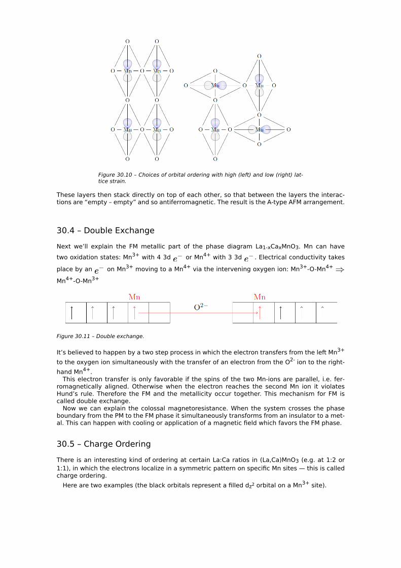
Figure 30.10 – Choices of orbital ordering with high (left) and low (right) lat-tice strain.
These layers then stack directly on top of each other, so that between the layers the interac-tions are “empty – empty” and so antiferromagnetic. The result is the A-type AFM arrangement.
30.4 – Double Exchange Next we’ll explain the FM metallic part of the phase diagram La1-xCaxMnO3. Mn can have two oxidation states: Mn3+ with 4 3d or Mn4+ with 3 3d . Electrical conductivity takes place by an on Mn3+ moving to a Mn4+ via the intervening oxygen ion: Mn3+-O-Mn4+ Mn4+-O-Mn3+
Figure 30.11 – Double exchange.
It’s believed to happen by a two step process in which the electron transfers from the left Mn3+
to the oxygen ion simultaneously with the transfer of an electron from the O2- ion to the right-hand Mn4+.
This electron transfer is only favorable if the spins of the two Mn-ions are parallel, i.e. fer-romagnetically aligned. Otherwise when the electron reaches the second Mn ion it violates Hund’s rule. Therefore the FM and the metallicity occur together. This mechanism for FM is called double exchange.
Now we can explain the colossal magnetoresistance. When the system crosses the phase boundary from the PM to the FM phase it simultaneously transforms from an insulator to a met-al. This can happen with cooling or application of a magnetic field which favors the FM phase.
30.5 – Charge Ordering There is an interesting kind of ordering at certain La:Ca ratios in (La,Ca)MnO3 (e.g. at 1:2 or 1:1), in which the electrons localize in a symmetric pattern on specific Mn sites — this is called charge ordering.
Here are two examples (the black orbitals represent a filled dz2 orbital on a Mn3+ site).

Figure 30.12 – Magnetic ordering for certain La:Ca ratios.
Since the electrons are localized, these special concentrations are insulating. In electron microscopy, the ordering of the Jahn-Teller distortions can be seen as characteristic stripes as shown here:
30.6 – LaMnO3 versus BiMnO3: Role of the Lone Pair Let’s look at the electronic structures of the La and Bi atoms and ions:
Bi3+ has the core electrons [Xe] (4f)14 (5d)10 and as valence electrons a pair of electrons in the 6s orbital. We call the (6s)2 electrons a lone pair.

You might recall the effect of such lone pairs from the behavior of ammonia, NH3: N has 5 valence electrons, of which 3 are bond covalently with H and 2 form a lone pair. A lone pair occupies space, makes a structural distortion and gives NH3 its dipole moment.
One can see the lone pairs in the calculated charge density of BiMnO3 as the yellow umbrella-shaped “blobs” next to the black Bi ions:
Figure 30.16 – The electron density map of BiMnO3 is given in the upper right: yellow parachute like structures are the lone pairs, Bi3+ are given as black dots.
Remember that in the case of LaMnO3, the arrangement of dz2 orbitals that minimized the lattice strain led to an A-type AFM ordering of the magnetic moments. In BiMnO3, there is an additional distortion from the Bi lone pairs, and a different orbital-ordering pattern is favored, as shown below. In fact, this orbital orbital ordering leads to a ferromagnetic ordering of the magnetic moments.
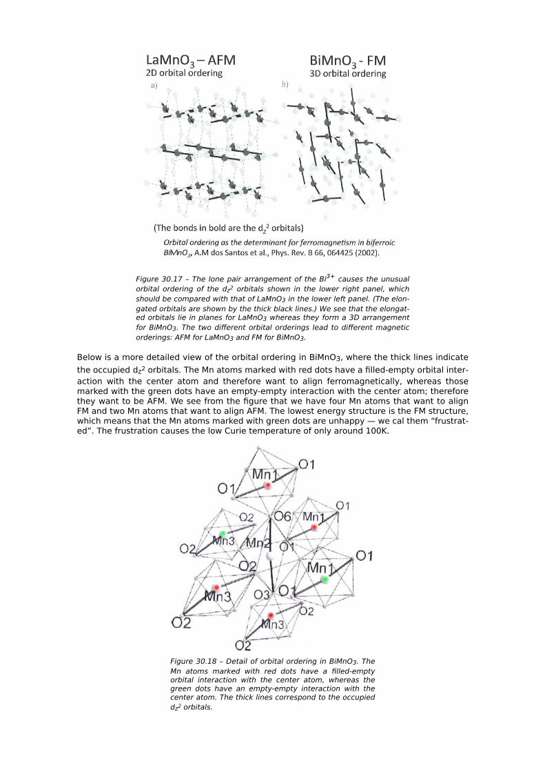
Figure 30.17 – The lone pair arrangement of the Bi3+ causes the unusual orbital ordering of the dz2 orbitals shown in the lower right panel, which should be compared with that of LaMnO3 in the lower left panel. (The elon-gated orbitals are shown by the thick black lines.) We see that the elongat-ed orbitals lie in planes for LaMnO3 whereas they form a 3D arrangement for BiMnO3. The two different orbital orderings lead to different magnetic orderings: AFM for LaMnO3 and FM for BiMnO3.
Below is a more detailed view of the orbital ordering in BiMnO3, where the thick lines indicate the occupied dz2 orbitals. The Mn atoms marked with red dots have a filled-empty orbital inter-action with the center atom and therefore want to align ferromagnetically, whereas those marked with the green dots have an empty-empty interaction with the center atom; therefore they want to be AFM. We see from the figure that we have four Mn atoms that want to align FM and two Mn atoms that want to align AFM. The lowest energy structure is the FM structure, which means that the Mn atoms marked with green dots are unhappy — we cal them “frustrat-ed”. The frustration causes the low Curie temperature of only around 100K.
Figure 30.18 – Detail of orbital ordering in BiMnO3. The Mn atoms marked with red dots have a filled-empty orbital interaction with the center atom, whereas the green dots have an empty-empty interaction with the center atom. The thick lines correspond to the occupied dz2 orbitals.

Missing Content: 3 interactive modules Visit eskript.ethz.ch to see everything.
An interactive or media element has been excluded from this version of the text. You can view it online here: https://wp-prd.let.ethz.ch/WP0-CIPRF91184/?p=170
An interactive or media element has been excluded from this version of the text. You can view it online here: https://wp-prd.let.ethz.ch/WP0-CIPRF91184/?p=170
An interactive or media element has been excluded from this version of the text. You can view it online here: https://wp-prd.let.ethz.ch/WP0-CIPRF91184/?p=170

31
How is AFM Ordering measured?
Neutron diffraction can be used to determine the magnetic ordering of a material because neu-trons have a magnetic moment and are therefore scattered at magnetic moments from elec-trons (X-rays are scattered at the electron density and are therefore not sensitive to magnetic moments).
So let’s look at a simple atomic structure. Using Bragg’s diffraction law:
Figure 31.1 – The Bragg diffraction from two layers of atoms is shown. Refraction peaks are only visible in directions which satisfy the Bragg condition.
we see from the figure above that Bragg diffraction only occurs at certain well-defined scatter-ing angles. In real crystals, the number of observed diffraction lines is lowered further due to symmetry considerations.
As an example, we take the reflection from the (100) planes of a bcc material.
Figure 31.2 – The Bragg reflection of (100) planes in bcc structure.
If we do not take the magnetic moments of the electrons into account (for example if the mate-rial is above the Néel temperature), then all atoms are identical and we see that the layers (1) and (3) are in-phase, but the reflection from the intermediate plane (2) is exactly out of phase. Therefore, the (100) reflection does not appear.
Let’s see what happens if the structure has an antiferromagnetic ordering, such that the sec-ond plane has opposite magnetic moment to the planes (1) and (3), below the Néel tempera-ture. Again, the second plane is out of phase, but this time it scatters neutrons with a different amplitude: it does not exactly cancel and we see the diffraction peak from the (100) planes. The symmetry lowering phase transition that occurs at TN causes extra lines to appear in the diffraction pattern. (We will come back to symmetry lowering phase transitions later in the con-text of ferroelectricity).
Some real neutron diffraction data are shown in the figure below for the case of MnO.

Figure 31.3 – Magnetic unit cell and neutron diffraction for MnO.
First we see that the magnetic unit cell (right) is larger than the chemical unit cell (left) because the up and down spin Mn ions are distinguishable and the neutrons see them as dif-ferent atoms. The resulting lower symmetry leads to additional peaks in the diffraction pattern (below) compared with the paramagnetic case (lower panel).
Neutron diffraction has in addition to the sensitivity to magnetic moments two additional advantages over x-ray diffraction: the neutron wavelength at room temperature is of the order of the spacing between atoms in the typical crystal structures and the neutron scattering amplitude varies in an irregular way with the atomic number. Therefore, we can distinguish magnetic moments of elements in a compound such as Fe and Co. The disadvantages are that the scattering intensity is lower, so one needs large single crystals, and also that neutron sources require large-scale facilities for their maintenance.

32
Summary
An interactive or media element has been excluded from this version of the text. You can view it online here: https://wp-prd.let.ethz.ch/WP0-CIPRF91184/?p=175
Solution: Have a look after having first tried yourself above! • The magnetic moment of an electron is either +µB or -µB (where µB is the Bohr
magneton) depending on whether it is down or up spin. • The Pauli Principle states that the total electronic wavefunction must be
antisymmetric with respect to the interchange of two electrons. • The magnetic exchange energy J has a role in explaining the magnetism of some
molecules, as it favours the parallel configuration of spins. • The ground state of atoms, ions or molecules can be magnetic when (i) 2J is larger
than the energy difference between states, (ii) there is an odd number of electrons and (iii) for degenerate orbitals.
• The term magnetoresistance refers to the change in electrical resistivity of a material when a magnetic field is applied.
• In general, d bands present a small energy cost to promote electrons into empty levels, and a large J as electrons are tightly bound. Therefore, d bands easily become magnetic.
• The origin of antiferromagnetic ordering in transition metal oxides is a phenomenon called superexchange, which is a consequence of the partial covalent bonding between the transition metal ion and the neighbouring oxygen ions.
• Antiferromagnetic ordering can be mesured by using neutron diffraction. • The double exchange mechanism favours the parallel ordering of neighbouring ions
and therefore ferromagnetism, as electrical conductivity can only take place in this situation.
• In certain occasions, electrons may localize in a symmetric pattern on specific ion sites. This phenomenon is called charge ordering, and since the electrons are localized, the system becomes insulating.

This is where you can add appendices or other back matter.