Embed Size (px)
Citation preview

POLITECNICO DI TORINO
MASTER’S THESIS
FPGA implementation of an A/D conversion and aPulse Width Modulation with interleaving
for a multiphase drive system
Author:Pietro MICELI
Supervisor:Dr.Francesco MUSOLINO
Dr. Luca PERETTI
A thesis submitted in fulfillment of the requirementsfor the Master of Science degree in Electronic Engineering
at the
Division of Electric Power and Energy SystemKTH Royal Institue of Technology
March 14, 2020

AbstractThe scientific context in which the thesis project takes place, is that of elec-tric machines. The work carried out is part of the realization of new con-figurations of asynchronous electric motors wound so as to allow the onlinechange of the number of phases and poles generated. Such a type of motoris commonly referred to as WICSC (Wound Indipendently-Controlled StatorCoils). The main application to which we can refer for this type of engine iscertainly the automotive field. The engine under study was designed to havea number of phases greater than or equal to three (commonly referred to as amultiphase machine).
The work presented in this thesis is based on the implementation onFPGA of two main structure preparatory to the realization of the completecontrol system of an induction machine with the capability of changing num-ber of phases and poles. The first structure implemented is related to the ac-quisition of the samples provided by a dedicated measurement system ableto measure the current flowing in each slot of the machine. The second struc-ture implements the Carrier Based Pulse Width Modulation. In the imple-mentation of the modulation section the technique of interleaving is used toimprove the overall performace. The implementation of the structures forsampling and sample management and for PWM modulation was carriedout on FPGA using the VHDL language. The realized structures are simu-lated first and subsequently verified with dedicated testbench. The work iscompleted by simulations in Matlab-Simulink in order to have This modeloffers the possibility of qualitatively evaluating the benefits introduced bythe interleaving modulation technique.
All the work has been carried at the division of Electric Power and EnergySystems in the department of Electrical Energy Engineering at KTH RoyalInstitute of Technology (Stockholm).

ii
Thesis Outilne
This thesis is divided in four main parts:
The firset part is devoted to a brief introduction on asynchronous electricmachines with particular emphasis on the structure of a multiphase machineand its advantages. Finally, the structure of the engine involved in the thesiswork is illustrated.
The second part concerns the two structures built for A/D conversion andfor the implementation of Pulse Width Modulation. For both sections, theinitial specifications and the proposed solutions are described by carefullyanalyzing the operation in detail and the techniques used. As for PWM mod-ulation, the interleaving technique and its benefits are introduced.
The third part of the thesis illustrates the model created in matlab-simulinkto evaluate the benefits introduced by the interleaving technique as a first ap-proximation. In particular, the stress reduction on the DC-bus and the inputcapacitors of the inverters are presented, as well as the reduction of lossesrelated to the THD improvements in the phase to phase voltage.
Last part expose the measurements obtained from two dedicated testbenchfor the analog to digital conversion and samples acquisition in the FPGA,as well as the verification of the functioning of the Pulse Width Modulation.The conclusion about the achievement obtained and the future developmentare finally presented.

iii
Contents
Abstract i
1 Multiphase Machine 11.1 Electrical machine . . . . . . . . . . . . . . . . . . . . . . . . . . 1
1.1.1 Induction motor . . . . . . . . . . . . . . . . . . . . . . 21.2 Overview of Multiphase Machines . . . . . . . . . . . . . . . . 31.3 Virtues of MPM . . . . . . . . . . . . . . . . . . . . . . . . . . . 5
1.3.1 The reduction of phase currents at constant power andvoltage levels . . . . . . . . . . . . . . . . . . . . . . . . 5
1.3.2 The machine manufacturing aspects . . . . . . . . . . . 61.3.3 The fault handling . . . . . . . . . . . . . . . . . . . . . 7
1.4 Overview of the motor involved . . . . . . . . . . . . . . . . . 8
2 Complete system overview 11
3 A/D conversion 133.1 Current sampling . . . . . . . . . . . . . . . . . . . . . . . . . . 13
3.1.1 Overview of measurement system . . . . . . . . . . . . 133.1.2 ADC choice . . . . . . . . . . . . . . . . . . . . . . . . . 143.1.3 Communication protocol . . . . . . . . . . . . . . . . . 153.1.4 Physical connection between FPGA and ADCs . . . . . 16
3.2 Sample acquisition . . . . . . . . . . . . . . . . . . . . . . . . . 173.2.1 Description of the structure created . . . . . . . . . . . 173.2.2 RTL view . . . . . . . . . . . . . . . . . . . . . . . . . . 183.2.3 Simulation results . . . . . . . . . . . . . . . . . . . . . 21
4 PWM signals generation 234.1 Carrier Based PWM . . . . . . . . . . . . . . . . . . . . . . . . . 234.2 Mapping of slots by configuration . . . . . . . . . . . . . . . . 254.3 Interleaving and benefits . . . . . . . . . . . . . . . . . . . . . . 26
4.3.1 Interleaving inside the phases . . . . . . . . . . . . . . . 274.3.2 Benefits . . . . . . . . . . . . . . . . . . . . . . . . . . . 30
4.4 Description of the structure implemented . . . . . . . . . . . . 314.5 RTL view . . . . . . . . . . . . . . . . . . . . . . . . . . . . . . . 344.6 Mechanism of configurations transition with smooth variation 36

iv
4.7 Simulation results . . . . . . . . . . . . . . . . . . . . . . . . . . 39
5 Simulink model for interleving benefits 435.1 Simulink model . . . . . . . . . . . . . . . . . . . . . . . . . . . 435.2 DC-bus and capacitors stress . . . . . . . . . . . . . . . . . . . 435.3 THD in phase to phase voltage . . . . . . . . . . . . . . . . . . 45
6 Measurements and results 516.1 A/D conversion Testbench . . . . . . . . . . . . . . . . . . . . . 516.2 PWM square waves analysis . . . . . . . . . . . . . . . . . . . . 52
6.2.1 Verification of PWM outputs . . . . . . . . . . . . . . . 536.2.2 FFT of PWM square waves . . . . . . . . . . . . . . . . 55
7 Conclusions 597.1 Improvement obtained . . . . . . . . . . . . . . . . . . . . . . . 597.2 Future works . . . . . . . . . . . . . . . . . . . . . . . . . . . . . 60
Bibliography 61

v
List of Figures
1.1 Typical winding pattern for a 3-phase 4-pole motor . . . . . . 31.2 Examples of symmetric multi-phase machines: (a)three-phase,
(b)five-phase, (c)seven-phase . . . . . . . . . . . . . . . . . . . 41.3 6-phase symmetric multi-phase machine . . . . . . . . . . . . . 41.4 Ten-phase split-phase machine (n=10, N=2, m=5) . . . . . . . . 51.5 Corner and axial view of the machine involved in the project . 81.6 Axial section of the machine involved in the project . . . . . . 9
2.1 System overview diagram . . . . . . . . . . . . . . . . . . . . . 12
3.1 Power board, top and bottom view (LEM sensors on the left) . 133.2 ADC, functional blockdiagram . . . . . . . . . . . . . . . . . . 143.3 Low voltage differetnail signal electric levels . . . . . . . . . . 153.4 Communication protocol, timing diagram . . . . . . . . . . . . 163.5 Samples acquiring system: overallview . . . . . . . . . . . . . 193.6 Sample acquiring system, high level RTL view . . . . . . . . . 203.7 Sampling section, RTL view . . . . . . . . . . . . . . . . . . . . 213.8 Sampling section. FSM chart . . . . . . . . . . . . . . . . . . . . 22
4.1 Sinusoidal carrier based PWM . . . . . . . . . . . . . . . . . . . 244.2 Line to line voltage spectrum in sinusoidal PWM . . . . . . . . 244.3 Slot mapping for 3-phase configurations . . . . . . . . . . . . . 274.4 Slot mapping for 6-phase configurations . . . . . . . . . . . . . 284.5 Slot mapping for 9-phase configurations . . . . . . . . . . . . . 284.6 Slot mapping for 18-phase 2-pole configuration . . . . . . . . . 294.7 Carrier to slot association in 3-phase configurations . . . . . . 294.8 Carrier to slot association in 6-phase configurations . . . . . . 304.9 Carrier to slot association in 9-phase configurations . . . . . . 304.10 Carrier to slot association in 18-phase configuration . . . . . . 314.11 PWM section overview . . . . . . . . . . . . . . . . . . . . . . . 324.12 Carrier generation, block diagram view . . . . . . . . . . . . . 324.13 Generic slot, block diagram view . . . . . . . . . . . . . . . . . 334.14 Configuration handler, FSM chart . . . . . . . . . . . . . . . . . 344.15 Carrier structure, Up and Down structures . . . . . . . . . . . 354.16 Generic slot, RTL view . . . . . . . . . . . . . . . . . . . . . . . 35
vi
4.17 Transition handler, FSM chart . . . . . . . . . . . . . . . . . . . 374.18 Carrier transition, m3p2 to m3p4, slot 8 . . . . . . . . . . . . . 384.19 Carriers with interleaving, 3-phases 2-poles . . . . . . . . . . . 404.20 Carriers with interleaving, 3-phases 6-poles . . . . . . . . . . . 404.21 PWM waves with interleaving, 3-phases 2-poles . . . . . . . . 404.22 PWM waves, 3-phases 2-poles phase A,B and C . . . . . . . . 414.23 Carrier transition from m3-p2 to m3-p12 configuration (slot 2
to 6) . . . . . . . . . . . . . . . . . . . . . . . . . . . . . . . . . . 41
5.1 Simulink model for interleaving benefits verification . . . . . . 445.2 DC-bus variation with and without interleaving . . . . . . . . 455.3 DC-bus capacitors current comparison in 3-phase 2-pole con-
figuration . . . . . . . . . . . . . . . . . . . . . . . . . . . . . . . 465.4 DC-bus capacitors current comparison in 3-phase configurations 465.5 Phase to phase voltage, 3-phases 2-poles configuration with-
out interleaving . . . . . . . . . . . . . . . . . . . . . . . . . . . 475.6 Phase to phase voltage, 3-phases 2-poles configuration with
standard interleaving . . . . . . . . . . . . . . . . . . . . . . . . 485.7 Phase to phase voltage, 3-phases 2-poles configuration with
interleaving inside the phases . . . . . . . . . . . . . . . . . . . 48
6.1 ADC samples - one period . . . . . . . . . . . . . . . . . . . . . 526.2 ADC samples - two period . . . . . . . . . . . . . . . . . . . . . 536.3 PWM signals (phase A, 3-phase 2-poles) . . . . . . . . . . . . . 546.4 PWM signals (phase A B and C, 3-phase 4-poles) . . . . . . . . 546.5 PWM signals, phase A1-A2-B1-B2-C1-C2, m3p2 (2 slots per
phase) . . . . . . . . . . . . . . . . . . . . . . . . . . . . . . . . . 556.6 PWM signals, transition m3p2 to m6p2 . . . . . . . . . . . . . 566.7 PWM output, m3p2 configuration, slot 1,13,25 . . . . . . . . . 566.8 Amplitude spectrum of PWM output, slot 1 m3p2 configuration 576.9 Amplitude spectrum of PWM output, m3p2 configuration, slot
1,13,25 (25kHz range) . . . . . . . . . . . . . . . . . . . . . . . . 576.10 Amplitude spectrum of PWM output, m3p2 configuration, slot
1,13,25 (9kHz range) . . . . . . . . . . . . . . . . . . . . . . . . 586.11 Phase spectrum of PWM output, m3p2 configuration, slot 1,13,25 58

vii
List of Abbreviations
A/D Analog to DigitalADC Analog to Digital ConverterCG Carrier GeneratorCH Configuration HandlerEVM Evaluation ModuleFFT Fast Fourier TransformFPGA Field Programmable Gate ArrayFSM Finite State MachineLVDS Low Voltage Differential SignalMPM Multiphase Machinemx-py x-phase y-polePB Power BoardPCB Printed Circuit BoardPWM Pulse Width Modulationqs Slot per pole per phaseRF Register FileRTL Register Transfer LevelTB Test BenchTH Transition HandlerTHD Total Harmonic DistortionVHDL Very High Speed Integrated Circuit Hardware Description Language


1
Chapter 1
Multiphase Machine
1.1 Electrical machine
An electric motor is an electrical machine that converts electrical energy intomechanical energy. Most electric motors operate through the interaction be-tween the motor’s magnetic field and electric current in a wire winding togenerate force in the form of rotation of a shaft. Electric motors can be pow-ered by direct current (DC) sources,such as from batteries, or by alternatingcurrent (AC) sources, such as a power grid, inverters or electrical genera-tors.Electromechanical energy conversion takes place via the medium of amagnetic field or an electric field, but most practical converters use magneticfield as the coupling medium between electrical and mechanical systems, thisis because the electric storing capacity of the magnetic field is much higherthan that of the electric field.
The main elements that characterize an electric motor are the following:
• Stator
• Rotor
• Airgap
• Windings
Stator:The stator is the stationary part of the motor’s electromagnetic circuit andusually consists of either windings or permanent magnets. The stator coreis made up of many thin metal sheets, called laminations. Laminations areused to reduce energy losses that would result if a solid core were used.
Rotor:In an electric motor, the moving part is the rotor, which turns the shaft to de-liver the mechanical power. The rotor usually has conductors laid into it thatcarry currents, which interact with the magnetic field of the stator to gener-ate the forces that turn the shaft. Alternatively, some rotors carry permanent
2 Chapter 1. Multiphase Machine
magnets, and the stator holds the conductors.
Airgap:The distance between the rotor and stator is called the air gap. The air gaphas important effects, and is generally as small as possible, as a large gaphas a strong negative effect on performance. It is the main source of the lowpower factor at which motors operate. The magnetizing current increaseswith the air gap. For this reason, the air gap should be minimal. Very smallgaps may pose mechanical problems in addition to noise and losses.
Windings:Windings are wires that are laid in coils, usually wrapped around a lami-nated soft iron magnetic core so as to form magnetic poles when energizedwith current.
1.1.1 Induction motor
An induction motor or asynchronous motor is an AC electric motor in whichthe electric current in the rotor needed to produce torque is obtained by elec-tromagnetic induction from the magnetic field of the stator winding (fig. 1.1).An induction motor can therefore be made without electrical connections tothe rotor. An induction motor’s rotor can be either wound type or squirrel-cage type.
In both induction and synchronous motors, the AC power supplied to themotor’s stator creates a magnetic field that rotates in synchronism with theAC oscillations. Whereas a synchronous motor’s rotor turns at the same rateas the stator field, an induction motor’s rotor rotates at a somewhat slowerspeed than the stator field. The induction motor stator’s magnetic field istherefore changing or rotating relative to the rotor. This induces an oppos-ing current in the induction motor’s rotor, in effect the motor’s secondarywinding, when the latter is short-circuited or closed through an externalimpedance.
The induced currents in the rotor windings in turn create magnetic fieldsin the rotor that react against the stator field. Due to Lenz’s Law, the direc-tion of the magnetic field created will be such as to oppose the change incurrent through the rotor windings. The cause of induced current in the ro-tor windings is the rotating stator magnetic field, so to oppose the changein rotor-winding currents the rotor will start to rotate in the direction of therotating stator magnetic field. The rotor accelerates until the magnitude ofinduced rotor current and torque balances the applied mechanical load onthe rotation of the rotor. Since rotation at synchronous speed would result inno induced rotor current, an induction motor always operates slightly slower

1.2. Overview of Multiphase Machines 3
than synchronous speed. The difference, or "slip," between actual and syn-chronous speed varies from about 0.5% to 5.0% for standard Design B torquecurve induction motors. For rotor currents to be induced, the speed of thephysical rotor must be lower than one of the stator’s rotating magnetic field;otherwise the magnetic field would not be moving relative to the rotor con-ductors and no currents would be induced. Slip, s, is defined as the differencebetween synchronous speed and operating speed, at the same frequency, ex-pressed in rpm, or in percentage or ratio of synchronous speed. [5]
FIGURE 1.1: Typical winding pattern for a 3-phase 4-pole motor
1.2 Overview of Multiphase Machines
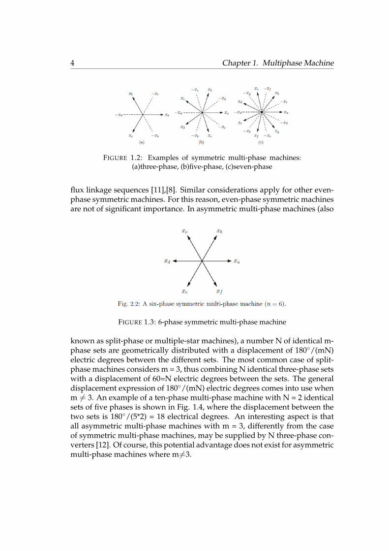
An electric machine with a total number of phases n > 3 is defined as multi-phase. There exist two main types of multi-phase machines: the symmetricand the asymmetric ones. In symmetric multi-phase machines, the phasesare equally distributed over the stator circumference with a displacementangle of 2π/n electric degrees. This machine type is an extension of theconventional symmetric three-phase machine shown in Fig. 1.2(a). The ar-rows represent the direction of the positive flux linkage in the machine phase,while the dashed lines indicate the negative flux linkage direction in the samephase. Fig. 1.3 shows the example of a six-phase symmetric multi-phase ma-chine, where it is evident that the phase couples a-d, b-e and c-f contribute(with opposite sign) to the same flux linkage, respectively. Such machine istopologically not different from a three-phase counterpart, since producingpositive flux linkage sequentially in the symmetric six-phase machine canbe equally achieved in the three-phase machine with positive and negative
4 Chapter 1. Multiphase Machine
FIGURE 1.2: Examples of symmetric multi-phase machines:(a)three-phase, (b)five-phase, (c)seven-phase
flux linkage sequences [11],[8]. Similar considerations apply for other even-phase symmetric machines. For this reason, even-phase symmetric machinesare not of significant importance. In asymmetric multi-phase machines (also
FIGURE 1.3: 6-phase symmetric multi-phase machine
known as split-phase or multiple-star machines), a number N of identical m-phase sets are geometrically distributed with a displacement of 180◦/(mN)electric degrees between the different sets. The most common case of split-phase machines considers m = 3, thus combining N identical three-phase setswith a displacement of 60=N electric degrees between the sets. The generaldisplacement expression of 180◦/(mN) electric degrees comes into use whenm 6= 3. An example of a ten-phase multi-phase machine with N = 2 identicalsets of five phases is shown in Fig. 1.4, where the displacement between thetwo sets is 180◦/(5*2) = 18 electrical degrees. An interesting aspect is thatall asymmetric multi-phase machines with m = 3, differently from the caseof symmetric multi-phase machines, may be supplied by N three-phase con-verters [12]. Of course, this potential advantage does not exist for asymmetricmulti-phase machines where m 6=3.

1.3. Virtues of MPM 5
FIGURE 1.4: Ten-phase split-phase machine (n=10, N=2, m=5)
1.3 Virtues of MPM
This section summarises the main potential advantages of multi-phase ma-chines and drives. Such benefits could translate into business advantages forsome specific systems and applications, and therefore must be consideredwith the perspective of the application and not as statements valid for anydrive system. In the last few years, a growing interest in multiphase machinehas been observed. Different reasons can explain this, the main ones can bethe following:
• The flied produced by stator excitation in a multiphase machine is char-acterized by a lower space-harmonic content, leading to an higher effi-ciency than in a three-phase machine;
• Multiphase machines are less susceptible than their three-phase coun-terparts to time-harmonic components in the excitation waveform;
• Multiphase machines have a greater fault tolerance than their three-phase counterparts [9].
1.3.1 The reduction of phase currents at constant power andvoltage levels
The first, and probably most straightforward, advantage of multi-phase ma-chines is the capability of lowering the current rating per phase by keepingthe same voltage and power ratings of a conventional three-phase machine.This is well summarised by the well-known equation of the active power in

6 Chapter 1. Multiphase Machine
a n-phase balanced system [16]:
p =12
uicos(φ) (1.1)
where p is the active power, u is the peak voltage, i is the peak current, andcos(φ) is the power factor. By keeping the same p and u values, and ap-proximately a similar power factor, it is immediate that lower values of i areobtained by increasing the phase number n. In principle, the reduction of thecurrent rating per phase allows the use of semiconductor technologies withlower current ratings as well. However, as the number of phases increase,also the number of frequency converters increase. This seem not to be a realissue in high-power systems, where already today several parallel convertersare used to feed a high-power three-phase machine.
1.3.2 The machine manufacturing aspects
While the electric aspects of splitting the power among n phases is well de-scribed by eqn. 1.1, the effect of a multi-phase design on the manufacturingof an electric machine is not as straightforward. The work in [10] helps in giv-ing a good overview of the relations between the design choices in an electricmachine. One of the most important equations obtained from the analysis isthe following:
pu = k(AsNt
bn) (1.2)
where k is a coefficient that does not depend on the winding structure of themachine, but only the magnetic, thermal and electrical loading of the ma-chine itself. Therefore, for machines with an homogeneous design in termsof thermal class, insulation technology, and effectiveness of the cooling sys-tem, k can be regarded approximately constant. This is actually confirmed ina series of design examples provided in [13]. The other parameters in eqn.1.2 are defined as follows:
• As is the slot cross-section area;
• Nt is the number of turns per coil;
• b is the number of parallel ways per phase;
• n, as before, is the number of phases.
According to eqn. 1.2, keeping a constant voltage u and increasing thepower p requires one of the following actions [12]:

1.3. Virtues of MPM 7
• increase As: by increasing the slot cross-sectional area, it is automaticthat the stator outer diameter is bound to grow too, in order to keepthe yoke flux density within acceptable values. Therefore, the overallmachine size increases too, making it not an optimal design choice;
• increase b: this strategy can be pursued as long as b is lower or equalto the number of poles 2p in the machine, which represents an upperlimit for the application of this design choice;
• decrease Nt: this can be achieved until Nt = 1.
• increase n: after the limitation b = 2p is reached, the only suitable wayleft to increase the rated power without machine size increase is to in-crement of the number of phases.
Thus, in some cases it may be useful to increase the power rating, at con-stant rated voltage, through an increment of n. In some high-power existingthree-phase systems, where many converter modules are already placed inparallel to fulfil the current requirements of the three-phase machine, thisdesign choice may lead to the use of the very same number of convertersconnected to a cheaper electric machine.
1.3.3 The fault handling
An important aspect when dealing with multi-phase machines is the poten-tial of fault tolerance operation that could arise by the use of n > 3 phases. Theprinciple is very basic and quite clear, as presented in [10],[9]: a multi-phasemachine can continue to operate with a rotating field as long as no more thann-3 phases are faulted. In other words, as long as a minimum of three phasescan be guaranteed, a rotating magnetic field can be produced to rotate themachine, although with different power/torque ratings. Clearly, the amountof power and torque that can be produced depends on the adopted faultstrategy, on the system topology as well as on the machine design. However,most of the time this type of fault handling requires a detection and a recon-figuration of the control, in order to compensate for the physical absence ofone phase in the control models.
8 Chapter 1. Multiphase Machine
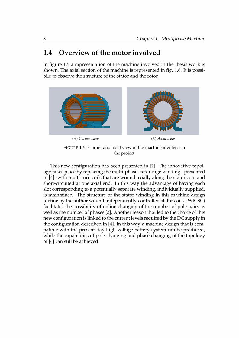
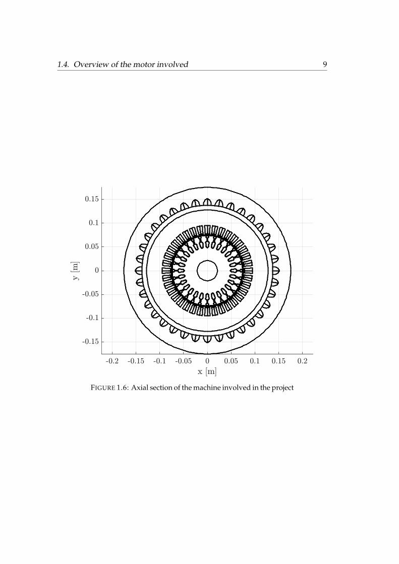
1.4 Overview of the motor involved
In figure 1.5 a rapresentation of the machine involved in the thesis work isshown. The axial section of the machine is represented in fig. 1.6. It is possi-bile to observe the structure of the stator and the rotor.
(A) Corner view (B) Axial view
FIGURE 1.5: Corner and axial view of the machine involved inthe project
This new configuration has been presented in [2]. The innovative topol-ogy takes place by replacing the multi-phase stator cage winding - presentedin [4]- with multi-turn coils that are wound axially along the stator core andshort-circuited at one axial end. In this way the advantage of having eachslot corresponding to a potentially separate winding, individually supplied,is maintained. The structure of the stator winding in this machine design(define by the author wound independently-controlled stator coils - WICSC)facilitates the possibility of online changing of the number of pole-pairs aswell as the number of phases [2]. Another reason that led to the choice of thisnew configuration is linked to the current levels required by the DC supply inthe configuration described in [4]. In this way, a machine design that is com-patible with the present-day high-voltage battery system can be produced,while the capabilities of pole-changing and phase-changing of the topologyof [4] can still be achieved.
1.4. Overview of the motor involved 9
FIGURE 1.6: Axial section of the machine involved in the project

11
Chapter 2
Complete system overview
Below is an overall description of the system to be implemented. Completedriving of an engine requires several sections. Starting from a higher level ofabstraction, the driving of a machine can be summarized as follows:
• Measurements of the quantities to be controlled;
• Processing of the control, starting from the physical quantities mea-sured;
• Realization of the drive control signals.
In our case, as with all more complete control systems, two control levelsare achieved: a current control and a speed control. The realization of thesemeasures requires a section dedicated to the necessary sensors, the condi-tioning of the analog signals obtained in preparation for the analog-digitalconversion and the electronics necessary for the AD conversion. Once thesamples are obtained, it is necessary to use a section capable of communicat-ing with the previous one, in order to acquire the digital signals and makeit possible to process this information for the management of the machinecontrol. The information above, once processed, provides the informationnecessary for the implementation of the modulation (in detail in the chap-ter 4). The modulation ends with the generation of the signals necessaryfor the inverters to suitably drive the machine. Considering that our multi-phase machine is made up of 36 slots, each of which is independently con-trolled, and that the signals to be supplied to the inverters for driving theIGBTs are signals with a high switching frequency, a section is introduced forthe transmission of these signals after a conversion of electrical informationinto optics. Everything is carried out mainly with a view to compliance withthe electromagnetic compatibility criteria. Below is a diagram to provide anoverview of the complete system (fig. 2.1): The realization of such a type ofsystem requires knowledge that ranges from the theory of electrical machinedesign, to the knowledge of driving techniques for electric drives, passingthrough knowledge of firmware programming for control via an FPGA pro-cessor and knowledge of hardware description languages, like the VHDL for
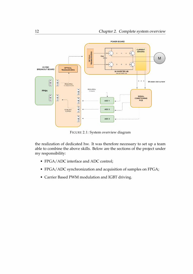
12 Chapter 2. Complete system overview
FIGURE 2.1: System overview diagram
the realization of dedicated hw. It was therefore necessary to set up a teamable to combine the above skills. Below are the sections of the project undermy responsibility:
• FPGA/ADC interface and ADC control;
• FPGA/ADC synchronization and acquisition of samples on FPGA;
• Carrier Based PWM modulation and IGBT driving.
13
Chapter 3
A/D conversion
3.1 Current sampling
3.1.1 Overview of measurement system
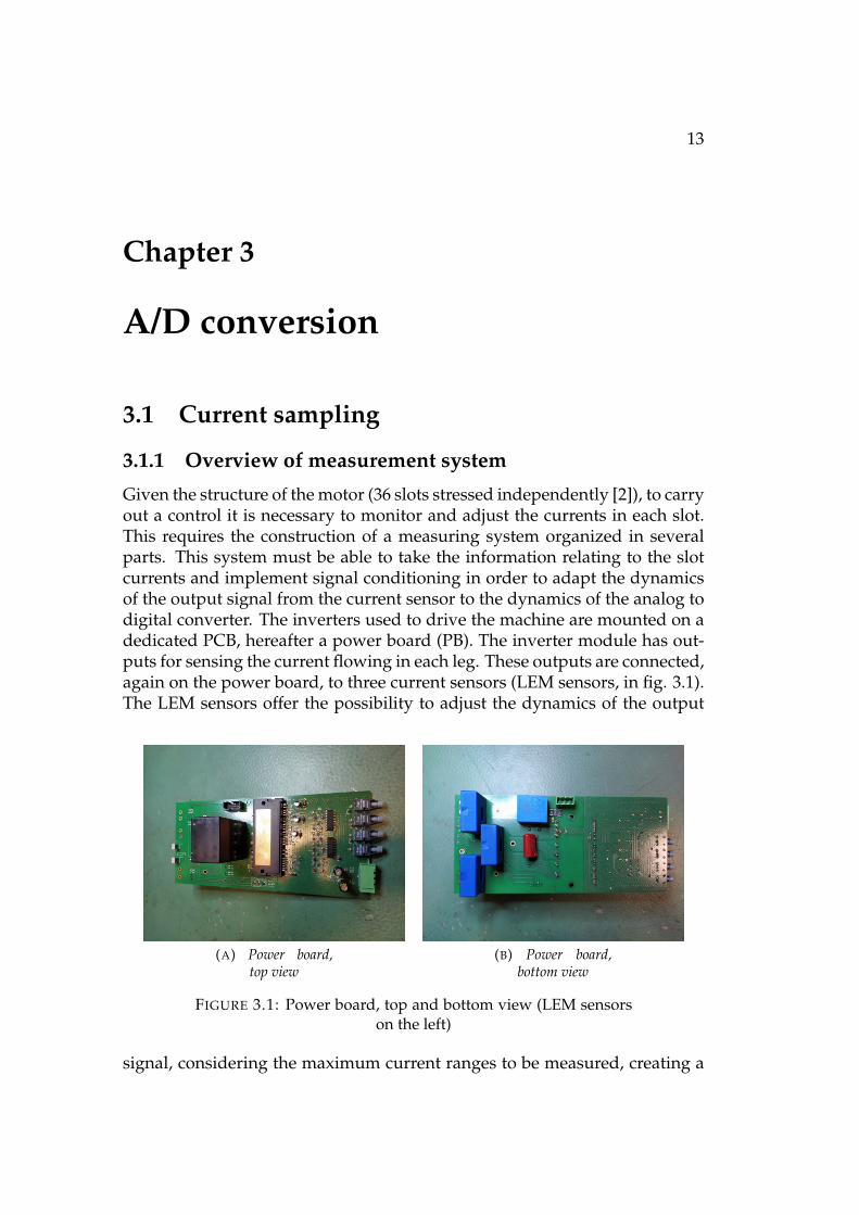
Given the structure of the motor (36 slots stressed independently [2]), to carryout a control it is necessary to monitor and adjust the currents in each slot.This requires the construction of a measuring system organized in severalparts. This system must be able to take the information relating to the slotcurrents and implement signal conditioning in order to adapt the dynamicsof the output signal from the current sensor to the dynamics of the analog todigital converter. The inverters used to drive the machine are mounted on adedicated PCB, hereafter a power board (PB). The inverter module has out-puts for sensing the current flowing in each leg. These outputs are connected,again on the power board, to three current sensors (LEM sensors, in fig. 3.1).The LEM sensors offer the possibility to adjust the dynamics of the output
(A) Power board,top view
(B) Power board,bottom view
FIGURE 3.1: Power board, top and bottom view (LEM sensorson the left)
signal, considering the maximum current ranges to be measured, creating a
14 Chapter 3. A/D conversion
variable number of windings around the sensor. The output of the currentsensors will go to the input of a PCB so that the conversion of the informationfrom current to voltage is carried out, passing through the gain adjustment soas to adapt the dynamics with that of the ADC and introducing componentsfor protection of the channels of the ADC.
3.1.2 ADC choice
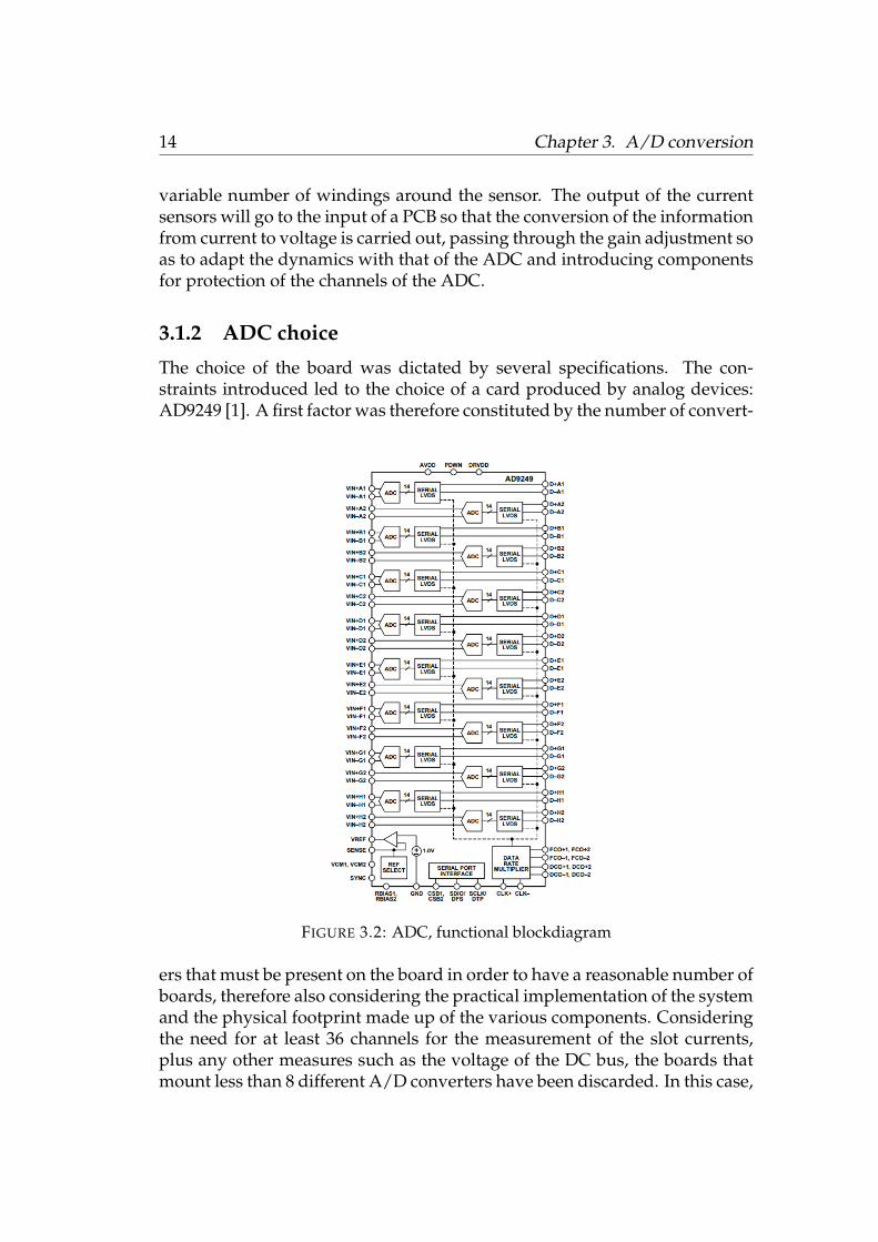
The choice of the board was dictated by several specifications. The con-straints introduced led to the choice of a card produced by analog devices:AD9249 [1]. A first factor was therefore constituted by the number of convert-
FIGURE 3.2: ADC, functional blockdiagram
ers that must be present on the board in order to have a reasonable number ofboards, therefore also considering the practical implementation of the systemand the physical footprint made up of the various components. Consideringthe need for at least 36 channels for the measurement of the slot currents,plus any other measures such as the voltage of the DC bus, the boards thatmount less than 8 different A/D converters have been discarded. In this case,
3.1. Current sampling 15
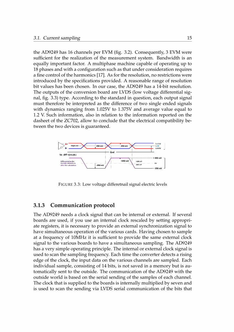
the AD9249 has 16 channels per EVM (fig. 3.2). Consequently, 3 EVM weresufficient for the realization of the measurement system. Bandwidth is anequally important factor. A multiphase machine capable of operating up to18 phases and with a configuration such as that under consideration requiresa fine control of the harmonics [17]. As for the resolution, no restrictions wereintroduced by the specifications provided. A reasonable range of resolutionbit values has been chosen. In our case, the AD9249 has a 14-bit resolution.The outputs of the conversion board are LVDS (low voltage differential sig-nal, fig. 3.3) type. According to the standard in question, each output signalmust therefore be interpreted as the difference of two single ended signalswith dynamics ranging from 1.025V to 1.375V and average value equal to1.2 V. Such information, also in relation to the information reported on thedasheet of the ZC702, allow to conclude that the electrical compatibility be-tween the two devices is guaranteed.
FIGURE 3.3: Low voltage differetnail signal electric levels
3.1.3 Communication protocol
The AD9249 needs a clock signal that can be internal or external. If severalboards are used, if you use an internal clock rescaled by setting appropri-ate registers, it is necessary to provide an external synchronization signal tohave simultaneous operation of the various cards. Having chosen to sampleat a frequency of 10MHz it is sufficient to provide the same external clocksignal to the various boards to have a simultaneous sampling. The AD9249has a very simple operating principle. The internal or external clock signal isused to scan the sampling frequency. Each time the converter detects a risingedge of the clock, the input data on the various channels are sampled. Eachindividual sample, consisting of 14 bits, is not saved in a memory but is au-tomatically sent to the outside. The communication of the AD9249 with theoutside world is based on the serial sending of the samples of each channel.The clock that is supplied to the boards is internally multiplied by seven andis used to scan the sending via LVDS serial communication of the bits that
16 Chapter 3. A/D conversion
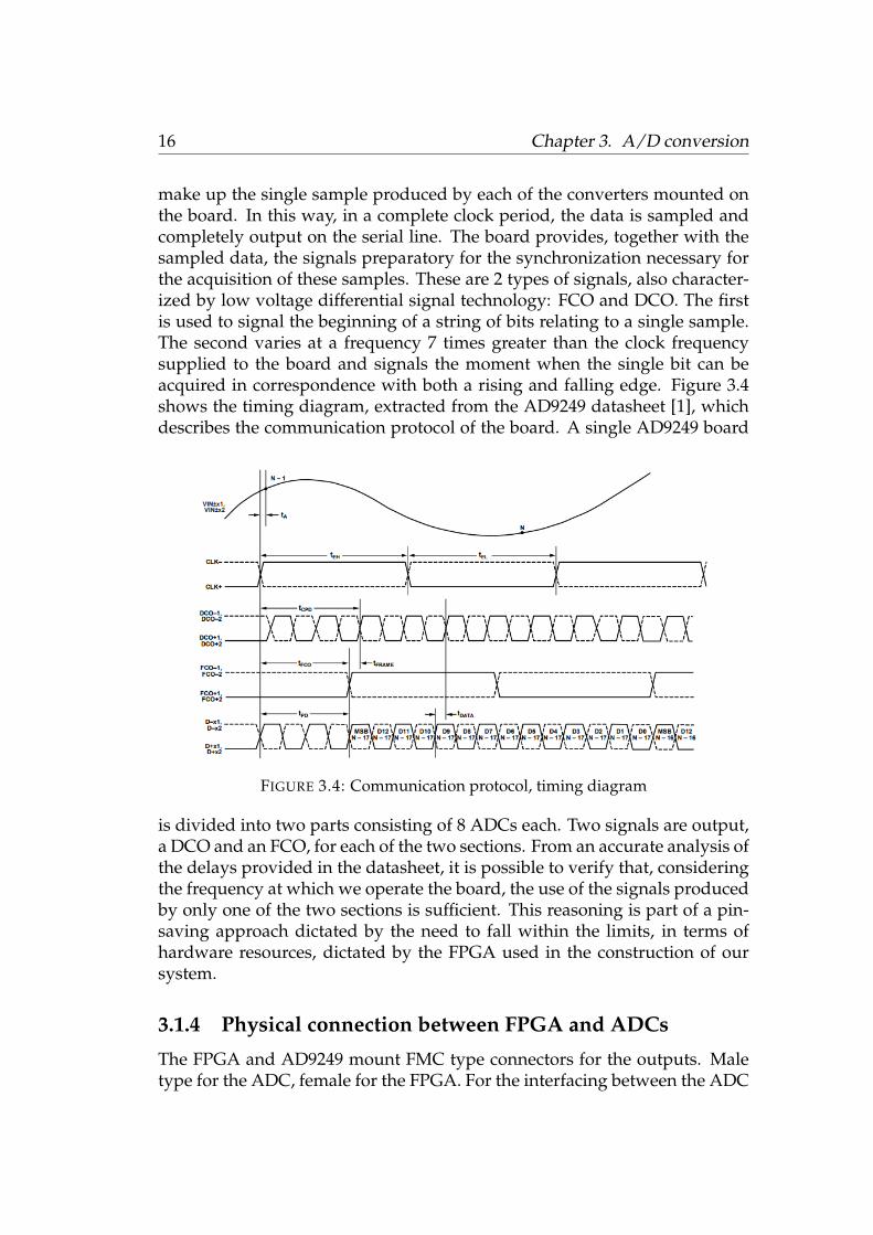
make up the single sample produced by each of the converters mounted onthe board. In this way, in a complete clock period, the data is sampled andcompletely output on the serial line. The board provides, together with thesampled data, the signals preparatory for the synchronization necessary forthe acquisition of these samples. These are 2 types of signals, also character-ized by low voltage differential signal technology: FCO and DCO. The firstis used to signal the beginning of a string of bits relating to a single sample.The second varies at a frequency 7 times greater than the clock frequencysupplied to the board and signals the moment when the single bit can beacquired in correspondence with both a rising and falling edge. Figure 3.4shows the timing diagram, extracted from the AD9249 datasheet [1], whichdescribes the communication protocol of the board. A single AD9249 board
FIGURE 3.4: Communication protocol, timing diagram
is divided into two parts consisting of 8 ADCs each. Two signals are output,a DCO and an FCO, for each of the two sections. From an accurate analysis ofthe delays provided in the datasheet, it is possible to verify that, consideringthe frequency at which we operate the board, the use of the signals producedby only one of the two sections is sufficient. This reasoning is part of a pin-saving approach dictated by the need to fall within the limits, in terms ofhardware resources, dictated by the FPGA used in the construction of oursystem.
3.1.4 Physical connection between FPGA and ADCs
The FPGA and AD9249 mount FMC type connectors for the outputs. Maletype for the ADC, female for the FPGA. For the interfacing between the ADC
3.2. Sample acquisition 17
boards and the FPGA it was necessary to create a dedicated PCB capable offulfilling the following functions:
• group the outputs of the three AD9249 (sampled data and synchroniza-tion signals) from three separate FMC connectors;
• sort the signals referred to in the previous point towards the two FMCsof the FPGA;
• routing a clock signal supplied by the zynq to the three adc boards (theclock signal is subsequently divided into three tracks each of whichends on SMA connectors compatible with the analog inputs of the ADCboards);
• connect the outputs of the zynq ZC702, dedicated to the production ofthe driving signals for the inverters, to the optical part which is respon-sible for transporting this information to the inverters.
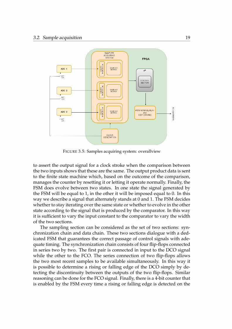
3.2 Sample acquisition
3.2.1 Description of the structure created
The structure created for data acquisition and communication between FPGAand ADC is divided into two main sections: the clock generator and the sam-pling section. In the first section, two signals are generated starting from thezynq ZC702 clock. The first is a clock signal, at the desired sampling fre-quency, which will be routed to the ADC. The latter, as defined in the com-munication protocol, will sample the data at the rising edges of this clock.The other generated signal can be set at a frequency lower than or equal to theclock supplied to the ADC and is a signal that is used by the sampling sectionfor the acquisition of the samples. The operation of the ADC provides thateach time the clock is received, the data on the various channels are sampledsynchronously and the samples of each channel are automatically sent in par-allel via serial communication. The decision to operate the ADC at a certainfrequency does not imply that there is always the need to acquire data at thisfrequency. The system created therefore allows to drive the ADC so that sam-ples at a certain frequency and to set a frequency equal to or lower to whichyou want to acquire the data. The second signal generated by the clock gen-erator will be the one capable of indicating to the sampling section the instantin which to start the data acquisition mechanism. As highlighted in section3.1.3, the ADC sends synchronization signals indicating when the data on theserial line can be considered valid and therefore acquired. The synchroniza-tion signals DCO and FCO can be used directly as clock of a structure that
18 Chapter 3. A/D conversion
acquires the bits on the serial line. In that case, however, it could occur thatthe information is corrupt due to noise or disturbances related to electromag-netic compatibility. In the structure built, it was therefore decided to treat theDCO and FCO as normal data, acquired and sampled using the FPGA clock.Using synchronization signals as data acquired through normal flip-flops re-duces the risk of malfunctions. If the signals are altered, they are sampledand kept until the next sampling, avoiding that they behave like a clock thatstarts certain operations every time a variation occurs. This decision allowsfor a more robust system at the expense of performance as a limit to the maxi-mum operating frequency is introduced. The DCO signal is in fact generatedby the ADC at a frequency equal to 7 times that of the clock. If you wantto treat the DCO as a data, it will be necessary to acquire it on the FPGA.Considering therefore the frequency of 200MHz of the clock on the ZC702 itis obtained that 14.2MHz is roughly the upper limit for the clock that is sentto the ADC and therefore to sampling, in fact: 100MHz/7≈14.2MHz.
3.2.2 RTL view
The structure created is instantiated three times since only three A/D boardsare used to measure the 36 currents flowing in the motor (one for each slot).For each of these there will be 12 channels for sending the bits that makeup the samples via serial communication. In the same way it is necessary toacquire on FPGA the synchronization signals that each of the ADC boardssends. In figure 3.5 it is possible to observe a first scheme to get a generaloverview of the structure built. The structure in detail is shown below, re-maining on an RTL abstraction level, and the operating principles that reg-ulate the clock generator and the sampling section. The clock generator isdivided into two blocks dedicated to the generation of two signals at differ-ent frequencies. Both frequencies can be changed by changing a parameterthat indicates how many FPGA clock edges (200MHz) must be counted inorder to rescale the clock at a lower frequency. The same structure is thenrepeated for both blocks and is as follows:
• Counter
• Comparator
• FSM
The counter is constantly enabled and each time the rising edge of the clockoccurs it increases the value of its output signal by one. This output goes tothe input of a comparator. The comparator has two inputs and one output.The two inputs consist of the counter output and a constant that is set accord-ing to the frequency of the signal to be obtained. The function of this block is
3.2. Sample acquisition 19
FIGURE 3.5: Samples acquiring system: overallview
to assert the output signal for a clock stroke when the comparison betweenthe two inputs shows that these are the same. The output product data is sentto the finite state machine which, based on the outcome of the comparison,manages the counter by resetting it or letting it operate normally. Finally, theFSM does evolve between two states. In one state the signal generated bythe FSM will be equal to 1, in the other it will be imposed equal to 0. In thisway we describe a signal that alternately stands at 0 and 1. The FSM decideswhether to stay iterating over the same state or whether to evolve in the otherstate according to the signal that is produced by the comparator. In this wayit is sufficient to vary the input constant to the comparator to vary the widthof the two sections.
The sampling section can be considered as the set of two sections: syn-chronization chain and data chain. These two sections dialogue with a ded-icated FSM that guarantees the correct passage of control signals with ade-quate timing. The synchronization chain consists of four flip-flops connectedin series two by two. The first pair is connected in input to the DCO signalwhile the other to the FCO. The series connection of two flip-flops allowsthe two most recent samples to be available simultaneously. In this way itis possible to determine a rising or falling edge of the DCO simply by de-tecting the discontinuity between the outputs of the two flip-flops. Similarreasoning can be done for the FCO signal. Finally, there is a 4-bit counter thatis enabled by the FSM every time a rising or falling edge is detected on the
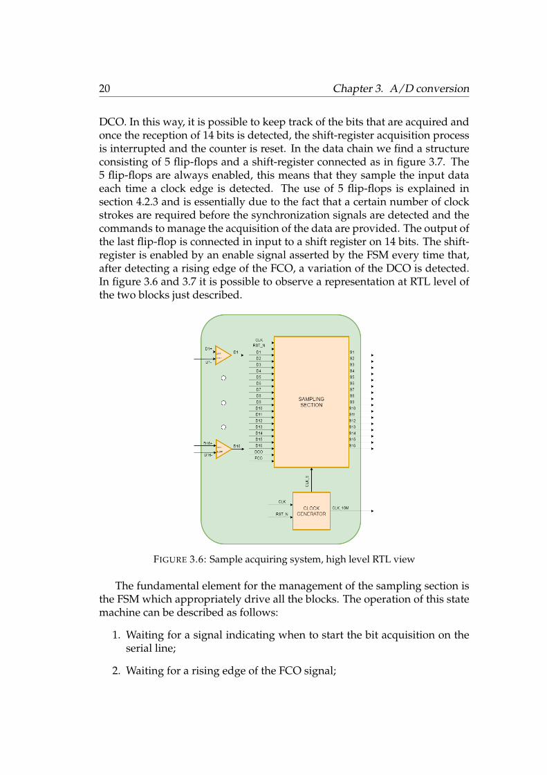
20 Chapter 3. A/D conversion
DCO. In this way, it is possible to keep track of the bits that are acquired andonce the reception of 14 bits is detected, the shift-register acquisition processis interrupted and the counter is reset. In the data chain we find a structureconsisting of 5 flip-flops and a shift-register connected as in figure 3.7. The5 flip-flops are always enabled, this means that they sample the input dataeach time a clock edge is detected. The use of 5 flip-flops is explained insection 4.2.3 and is essentially due to the fact that a certain number of clockstrokes are required before the synchronization signals are detected and thecommands to manage the acquisition of the data are provided. The output ofthe last flip-flop is connected in input to a shift register on 14 bits. The shift-register is enabled by an enable signal asserted by the FSM every time that,after detecting a rising edge of the FCO, a variation of the DCO is detected.In figure 3.6 and 3.7 it is possible to observe a representation at RTL level ofthe two blocks just described.
FIGURE 3.6: Sample acquiring system, high level RTL view
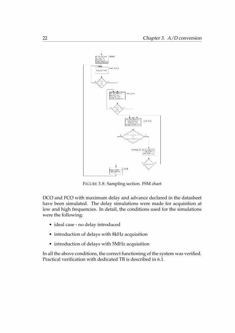
The fundamental element for the management of the sampling section isthe FSM which appropriately drive all the blocks. The operation of this statemachine can be described as follows:
1. Waiting for a signal indicating when to start the bit acquisition on theserial line;
2. Waiting for a rising edge of the FCO signal;
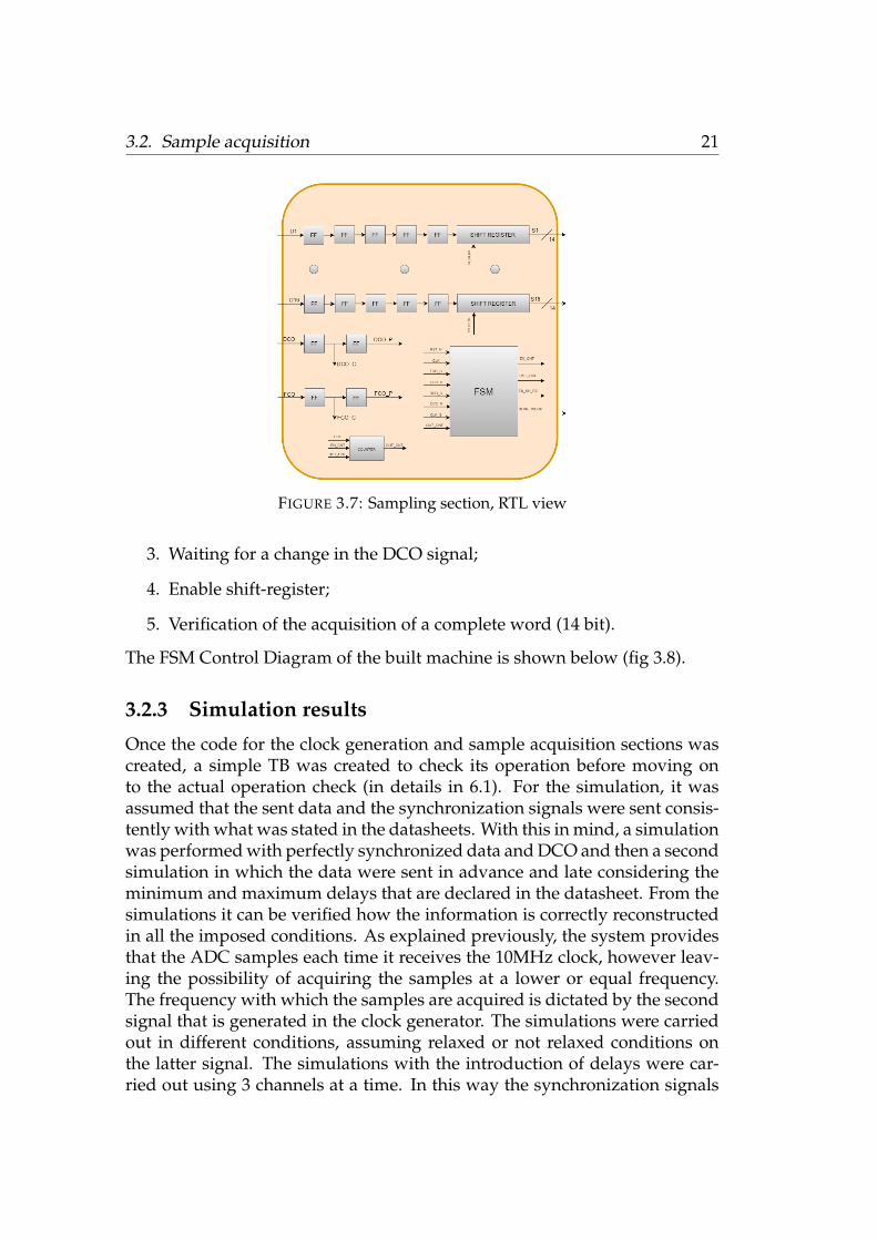
3.2. Sample acquisition 21
FIGURE 3.7: Sampling section, RTL view
3. Waiting for a change in the DCO signal;
4. Enable shift-register;
5. Verification of the acquisition of a complete word (14 bit).
The FSM Control Diagram of the built machine is shown below (fig 3.8).
3.2.3 Simulation results
Once the code for the clock generation and sample acquisition sections wascreated, a simple TB was created to check its operation before moving onto the actual operation check (in details in 6.1). For the simulation, it wasassumed that the sent data and the synchronization signals were sent consis-tently with what was stated in the datasheets. With this in mind, a simulationwas performed with perfectly synchronized data and DCO and then a secondsimulation in which the data were sent in advance and late considering theminimum and maximum delays that are declared in the datasheet. From thesimulations it can be verified how the information is correctly reconstructedin all the imposed conditions. As explained previously, the system providesthat the ADC samples each time it receives the 10MHz clock, however leav-ing the possibility of acquiring the samples at a lower or equal frequency.The frequency with which the samples are acquired is dictated by the secondsignal that is generated in the clock generator. The simulations were carriedout in different conditions, assuming relaxed or not relaxed conditions onthe latter signal. The simulations with the introduction of delays were car-ried out using 3 channels at a time. In this way the synchronization signals
22 Chapter 3. A/D conversion
FIGURE 3.8: Sampling section. FSM chart
DCO and FCO with maximum delay and advance declared in the datasheethave been simulated. The delay simulations were made for acquisition atlow and high frequencies. In detail, the conditions used for the simulationswere the following:
• ideal case - no delay introduced
• introduction of delays with 8kHz acquisition
• introduction of delays with 5MHz acquisition
In all the above conditions, the correct functioning of the system was verified.Practical verification with dedicated TB is described in 6.1.
23
Chapter 4
PWM signals generation
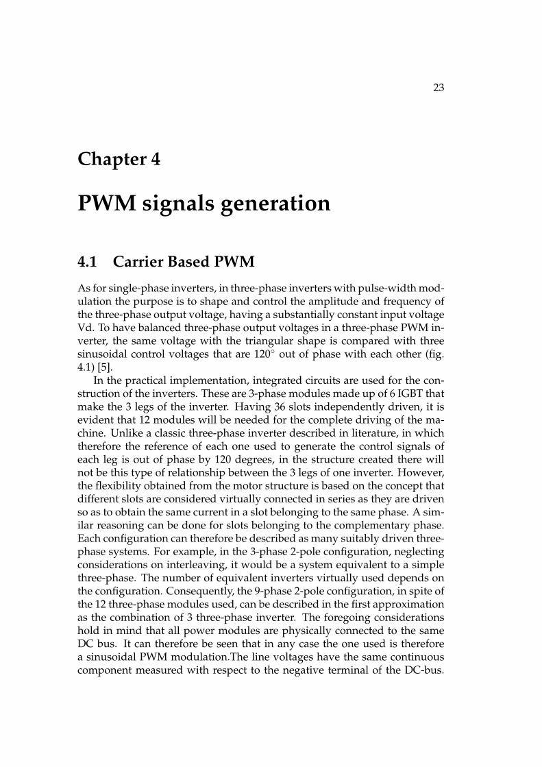
4.1 Carrier Based PWM
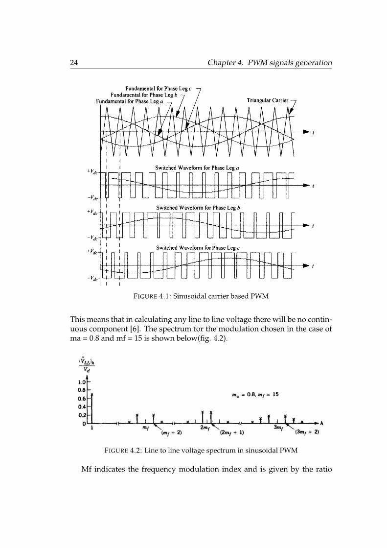
As for single-phase inverters, in three-phase inverters with pulse-width mod-ulation the purpose is to shape and control the amplitude and frequency ofthe three-phase output voltage, having a substantially constant input voltageVd. To have balanced three-phase output voltages in a three-phase PWM in-verter, the same voltage with the triangular shape is compared with threesinusoidal control voltages that are 120◦ out of phase with each other (fig.4.1) [5].
In the practical implementation, integrated circuits are used for the con-struction of the inverters. These are 3-phase modules made up of 6 IGBT thatmake the 3 legs of the inverter. Having 36 slots independently driven, it isevident that 12 modules will be needed for the complete driving of the ma-chine. Unlike a classic three-phase inverter described in literature, in whichtherefore the reference of each one used to generate the control signals ofeach leg is out of phase by 120 degrees, in the structure created there willnot be this type of relationship between the 3 legs of one inverter. However,the flexibility obtained from the motor structure is based on the concept thatdifferent slots are considered virtually connected in series as they are drivenso as to obtain the same current in a slot belonging to the same phase. A sim-ilar reasoning can be done for slots belonging to the complementary phase.Each configuration can therefore be described as many suitably driven three-phase systems. For example, in the 3-phase 2-pole configuration, neglectingconsiderations on interleaving, it would be a system equivalent to a simplethree-phase. The number of equivalent inverters virtually used depends onthe configuration. Consequently, the 9-phase 2-pole configuration, in spite ofthe 12 three-phase modules used, can be described in the first approximationas the combination of 3 three-phase inverter. The foregoing considerationshold in mind that all power modules are physically connected to the sameDC bus. It can therefore be seen that in any case the one used is thereforea sinusoidal PWM modulation.The line voltages have the same continuouscomponent measured with respect to the negative terminal of the DC-bus.
24 Chapter 4. PWM signals generation
FIGURE 4.1: Sinusoidal carrier based PWM
This means that in calculating any line to line voltage there will be no contin-uous component [6]. The spectrum for the modulation chosen in the case ofma = 0.8 and mf = 15 is shown below(fig. 4.2).
FIGURE 4.2: Line to line voltage spectrum in sinusoidal PWM
Mf indicates the frequency modulation index and is given by the ratio
4.2. Mapping of slots by configuration 25
between fsw and f01 (reference signal frequency). With appropriate precau-tions it is possible to alter the spectrum in order to reduce or eliminate somecomponents. In three-phase inverters, only the harmonics in the connectedvoltages are affected. Considering only the mf harmonic (the same consid-eration can be applied for odd multiples), the phase shift between the mfharmonic of two line voltages is equal to 120◦*Mf. This phase shift is zero ifmf is odd and is a multiple of three. It follows that the mf harmonic in theline voltage is zero [6]. Similar reasoning can be done for the suppression ofharmonics that are odd multiples of mf if an odd and multiple of three valueof mf is chosen. In this way it is found that some of the dominant harmonicsin a single-branch inverter can be eliminated from the connected voltage of athree-phase inverter.
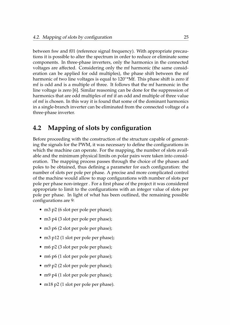
4.2 Mapping of slots by configuration
Before proceeding with the construction of the structure capable of generat-ing the signals for the PWM, it was necessary to define the configurations inwhich the machine can operate. For the mapping, the number of slots avail-able and the minimum physical limits on polar pairs were taken into consid-eration. The mapping process passes through the choice of the phases andpoles to be obtained, thus defining a parameter for each configuration: thenumber of slots per pole per phase. A precise and more complicated controlof the machine would allow to map configurations with number of slots perpole per phase non-integer . For a first phase of the project it was consideredappropriate to limit to the configurations with an integer value of slots perpole per phase. In light of what has been outlined, the remaining possibleconfigurations are 9:
• m3 p2 (6 slot per pole per phase);
• m3 p4 (3 slot per pole per phase);
• m3 p6 (2 slot per pole per phase);
• m3 p12 (1 slot per pole per phase);
• m6 p2 (3 slot per pole per phase);
• m6 p6 (1 slot per pole per phase);
• m9 p2 (2 slot per pole per phase);
• m9 p4 (1 slot per pole per phase);
• m18 p2 (1 slot per pole per phase).
26 Chapter 4. PWM signals generation
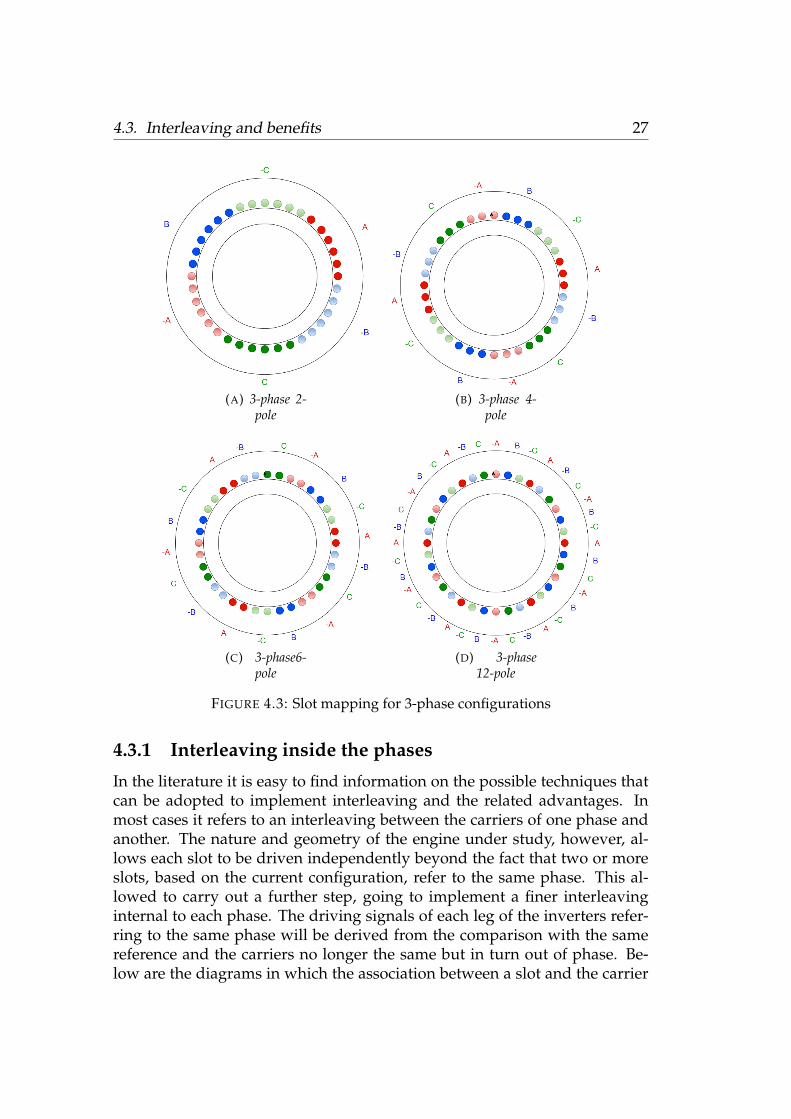
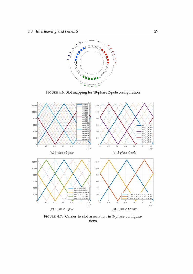
Once the possible configurations were defined, the mapping has been per-formed. From the previous list it can be seen that all possible configurationsare characterized by a number of phases equal to or multiple of 3. This fa-cilitates us in some situations where, due to the geometry of the machine,redundant configurations would be obtained. An example is certainly the6-phase case. In fact, a configuration with 6 phases cannot be realized withthe same procedure with which the slots are assigned for a three-phase mo-tor since it would be that a generic phase should be assigned to the slots towhich the complement of a phase already assigned corresponds(1.3). In thesecases, the machine is mapped as two three-phase systems out of phase witheach other. The phase angle between the two systems is calculated as [12]:360◦/(Nmp), where N is the number of identical m-phase sets and p is thenumber of poles. In the case of m6p2 and m6p6 (fig. 4.4) therefore the twothree-phase systems are out of phase with each other by 30 degrees and 10degrees respectively. The same problem occurs in the case m18 p2 in whichone proceeds by assigning the slots to six three-phase systems out of phaseby 10 degrees. The graphs of the slot assignments for each configuration areshown below (figures 4.3, 4.4, 4.5, 4.6).
4.3 Interleaving and benefits
Pulse-width modulation (PWM) is the ground for control in power electron-ics. The vast majority of semiconductor power devices in power electroniccircuits are controlled by pulse-width modulation signals of various forms.The fast rising and falling edges of the pulse-width modulation pulses en-sure that the power semiconductor devices are turned on/off as quickly aspossible to minimize the switching transition time and the associated switch-ing losses. Pulse-width modulation can take different forms. When multiplePWM converters are connected in parallel with current sharing, it is advan-tageous to operate all converters at the same switching frequency but withcontrollable phase shift these PWM signals. This technique is referred to asinterleaving PWM and has been widely used in power electronics [6],[7]. In-terleaved techniques provide many benefits for power converters, such asimproved efficiency with current sharing, reduction of output inductor withreduced inductor current ripples [14], [3], reduction of input DC-bus capaci-tor [15] with reduced input current ripples, and reduced common-mode volt-age. FPGA-based digital control technique with its high accurate and pro-grammable timing control capabilities exhibits significant advantages overconventional analog control technique when applying to multi-phase inter-leaved PWM inverter to achieving high power density inverter modules.
4.3. Interleaving and benefits 27
(A) 3-phase 2-pole
(B) 3-phase 4-pole
(C) 3-phase6-pole
(D) 3-phase12-pole
FIGURE 4.3: Slot mapping for 3-phase configurations
4.3.1 Interleaving inside the phases
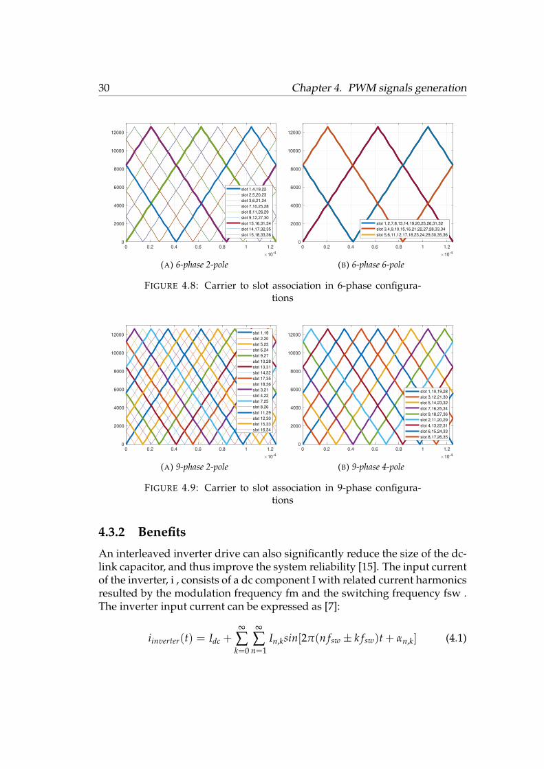
In the literature it is easy to find information on the possible techniques thatcan be adopted to implement interleaving and the related advantages. Inmost cases it refers to an interleaving between the carriers of one phase andanother. The nature and geometry of the engine under study, however, al-lows each slot to be driven independently beyond the fact that two or moreslots, based on the current configuration, refer to the same phase. This al-lowed to carry out a further step, going to implement a finer interleavinginternal to each phase. The driving signals of each leg of the inverters refer-ring to the same phase will be derived from the comparison with the samereference and the carriers no longer the same but in turn out of phase. Be-low are the diagrams in which the association between a slot and the carrier
28 Chapter 4. PWM signals generation
(A) 6-phase 2-pole
(B) 6-phase 6-pole
FIGURE 4.4: Slot mapping for 6-phase configurations
(A) 9-phase 2-pole
(B) 9-phase 4-pole
FIGURE 4.5: Slot mapping for 9-phase configurations
used to drive it when the configuration changes is defined (figures 4.7, 4.8,4.9, 4.10):
4.3. Interleaving and benefits 29
FIGURE 4.6: Slot mapping for 18-phase 2-pole configuration
0 0.2 0.4 0.6 0.8 1 1.2
10-4
0
2000
4000
6000
8000
10000
12000slot 1,19
slot 2,20
slot 3,21
slot 4,22
slot 5,23
slot 6,24
slot 7,25
slot 8,26
slot 9,27
slot 10,28
slot 11,29
slot 12,30
slot 13,31
slot 14,32
slot 15,33
slot 16,34
slot 17,35
slot 18,36
(A) 3-phase 2-pole
0 0.2 0.4 0.6 0.8 1 1.2
10-4
0
2000
4000
6000
8000
10000
12000
slot 1,10,19,28
slot 2,11,20,29
slot 3,12,21,30
slot 4,13,22,31
slot 5,14,23,32
slot 6,15,24,33
slot 7,16,25,34
slot 8,17,26,35
slot 9,18,27,36
(B) 3-phase 4-pole
0 0.2 0.4 0.6 0.8 1 1.2
10-4
0
2000
4000
6000
8000
10000
12000
slot 1,7,13,19,25,31
slot 2,8,14,20,26,32
slot 3,9,15,21,27,28,34
slot 4,10,16,22,28,34
slot 5,11,17,23,29,35
slot 6,12,18,24,30,36
(C) 3-phase 6-pole
0 0.2 0.4 0.6 0.8 1 1.2
10-4
0
2000
4000
6000
8000
10000
12000
slot 1,4,7,10,13,16,19,22,25,28,31,34
slot 2,5,8,11,14,17,20,23,26,29,32,35
slot 3,6,9,12,15,18,21,24,27,30,33,36
(D) 3-phase 12-pole
FIGURE 4.7: Carrier to slot association in 3-phase configura-tions
30 Chapter 4. PWM signals generation
0 0.2 0.4 0.6 0.8 1 1.2
10-4
0
2000
4000
6000
8000
10000
12000
slot 1,4,19,22
slot 2,5,20,23
slot 3,6,21,24
slot 7,10,25,28
slot 8,11,26,29
slot 9,12,27,30
slot 13,16,31,34
slot 14,17,32,35
slot 15,18,33,36
(A) 6-phase 2-pole
0 0.2 0.4 0.6 0.8 1 1.2
10-4
0
2000
4000
6000
8000
10000
12000
slot 1,2,7,8,13,14,19,20,25,26,31,32
slot 3,4,9,10,15,16,21,22,27,28,33,34
slot 5,6,11,12,17,18,23,24,29,30,35,36
(B) 6-phase 6-pole
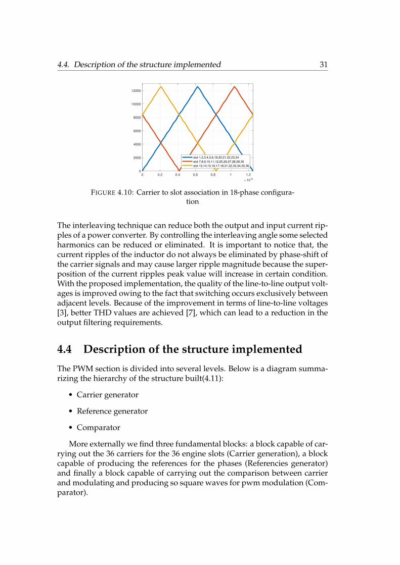
FIGURE 4.8: Carrier to slot association in 6-phase configura-tions
0 0.2 0.4 0.6 0.8 1 1.2
10-4
0
2000
4000
6000
8000
10000
12000slot 1,19
slot 2,20
slot 5,23
slot 6,24
slot 9,27
slot 10,28
slot 13,31
slot 14,32
slot 17,35
slot 18,36
slot 3,21
slot 4,22
slot 7,25
slot 8,26
slot 11,29
slot 12,30
slot 15,33
slot 16,34
(A) 9-phase 2-pole
0 0.2 0.4 0.6 0.8 1 1.2
10-4
0
2000
4000
6000
8000
10000
12000
slot 1,10,19,28
slot 3,12,21,30
slot 5,14,23,32
slot 7,16,25,34
slot 9,18,27,36
slot 2,11,20,29
slot 4,13,22,31
slot 6,15,24,33
slot 8,17,26,35
(B) 9-phase 4-pole
FIGURE 4.9: Carrier to slot association in 9-phase configura-tions
4.3.2 Benefits
An interleaved inverter drive can also significantly reduce the size of the dc-link capacitor, and thus improve the system reliability [15]. The input currentof the inverter, i , consists of a dc component I with related current harmonicsresulted by the modulation frequency fm and the switching frequency fsw .The inverter input current can be expressed as [7]:
iinverter(t) = Idc +∞
∑k=0
∞
∑n=1
In,ksin[2π(n fsw ± k fsw)t + αn,k] (4.1)
4.4. Description of the structure implemented 31
0 0.2 0.4 0.6 0.8 1 1.2
10-4
0
2000
4000
6000
8000
10000
12000
slot 1,2,3,4,5,6,19,20,21,22,23,24
slot 7,8,9,10,11,12,25,26,27,28,29,30
slot 13,14,15,16,17,18,31,32,33,34,35,36
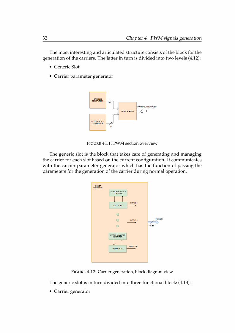
FIGURE 4.10: Carrier to slot association in 18-phase configura-tion
The interleaving technique can reduce both the output and input current rip-ples of a power converter. By controlling the interleaving angle some selectedharmonics can be reduced or eliminated. It is important to notice that, thecurrent ripples of the inductor do not always be eliminated by phase-shift ofthe carrier signals and may cause larger ripple magnitude because the super-position of the current ripples peak value will increase in certain condition.With the proposed implementation, the quality of the line-to-line output volt-ages is improved owing to the fact that switching occurs exclusively betweenadjacent levels. Because of the improvement in terms of line-to-line voltages[3], better THD values are achieved [7], which can lead to a reduction in theoutput filtering requirements.
4.4 Description of the structure implemented
The PWM section is divided into several levels. Below is a diagram summa-rizing the hierarchy of the structure built(4.11):
• Carrier generator
• Reference generator
• Comparator
More externally we find three fundamental blocks: a block capable of car-rying out the 36 carriers for the 36 engine slots (Carrier generation), a blockcapable of producing the references for the phases (Referencies generator)and finally a block capable of carrying out the comparison between carrierand modulating and producing so square waves for pwm modulation (Com-parator).
32 Chapter 4. PWM signals generation
The most interesting and articulated structure consists of the block for thegeneration of the carriers. The latter in turn is divided into two levels (4.12):
• Generic Slot
• Carrier parameter generator
FIGURE 4.11: PWM section overview
The generic slot is the block that takes care of generating and managingthe carrier for each slot based on the current configuration. It communicateswith the carrier parameter generator which has the function of passing theparameters for the generation of the carrier during normal operation.
FIGURE 4.12: Carrier generation, block diagram view
The generic slot is in turn divided into three functional blocks(4.13):
• Carrier generator
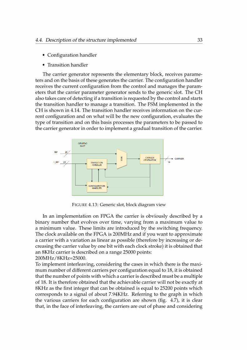
4.4. Description of the structure implemented 33
• Configuration handler
• Transition handler
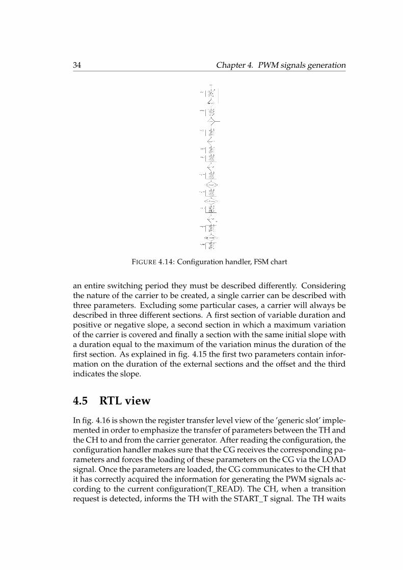
The carrier generator represents the elementary block, receives parame-ters and on the basis of these generates the carrier. The configuration handlerreceives the current configuration from the control and manages the param-eters that the carrier parameter generator sends to the generic slot. The CHalso takes care of detecting if a transition is requested by the control and startsthe transition handler to manage a transition. The FSM implemented in theCH is shown in 4.14. The transition handler receives information on the cur-rent configuration and on what will be the new configuration, evaluates thetype of transition and on this basis processes the parameters to be passed tothe carrier generator in order to implement a gradual transition of the carrier.
FIGURE 4.13: Generic slot, block diagram view
In an implementation on FPGA the carrier is obviously described by abinary number that evolves over time, varying from a maximum value toa minimum value. These limits are introduced by the switching frequency.The clock available on the FPGA is 200MHz and if you want to approximatea carrier with a variation as linear as possible (therefore by increasing or de-creasing the carrier value by one bit with each clock stroke) it is obtained thatan 8KHz carrier is described on a range 25000 points:200MHz/8KHz=25000.To implement interleaving, considering the cases in which there is the maxi-mum number of different carriers per configuration equal to 18, it is obtainedthat the number of points with which a carrier is described must be a multipleof 18. It is therefore obtained that the achievable carrier will not be exactly at8KHz as the first integer that can be obtained is equal to 25200 points whichcorresponds to a signal of about 7.94KHz. Referring to the graph in whichthe various carriers for each configuration are shown (fig. 4.7), it is clearthat, in the face of interleaving, the carriers are out of phase and considering
34 Chapter 4. PWM signals generation
FIGURE 4.14: Configuration handler, FSM chart
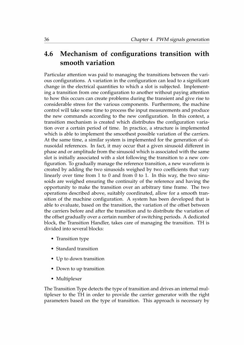
an entire switching period they must be described differently. Consideringthe nature of the carrier to be created, a single carrier can be described withthree parameters. Excluding some particular cases, a carrier will always bedescribed in three different sections. A first section of variable duration andpositive or negative slope, a second section in which a maximum variationof the carrier is covered and finally a section with the same initial slope witha duration equal to the maximum of the variation minus the duration of thefirst section. As explained in fig. 4.15 the first two parameters contain infor-mation on the duration of the external sections and the offset and the thirdindicates the slope.
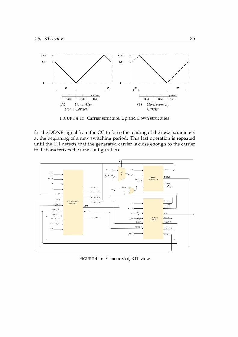
4.5 RTL view
In fig. 4.16 is shown the register transfer level view of the ’generic slot’ imple-mented in order to emphasize the transfer of parameters between the TH andthe CH to and from the carrier generator. After reading the configuration, theconfiguration handler makes sure that the CG receives the corresponding pa-rameters and forces the loading of these parameters on the CG via the LOADsignal. Once the parameters are loaded, the CG communicates to the CH thatit has correctly acquired the information for generating the PWM signals ac-cording to the current configuration(T_READ). The CH, when a transitionrequest is detected, informs the TH with the START_T signal. The TH waits
4.5. RTL view 35
(A) Down-Up-Down Carrier
(B) Up-Down-UpCarrier
FIGURE 4.15: Carrier structure, Up and Down structures
for the DONE signal from the CG to force the loading of the new parametersat the beginning of a new switching period. This last operation is repeateduntil the TH detects that the generated carrier is close enough to the carrierthat characterizes the new configuration.
FIGURE 4.16: Generic slot, RTL view
36 Chapter 4. PWM signals generation
4.6 Mechanism of configurations transition withsmooth variation
Particular attention was paid to managing the transitions between the vari-ous configurations. A variation in the configuration can lead to a significantchange in the electrical quantities to which a slot is subjected. Implement-ing a transition from one configuration to another without paying attentionto how this occurs can create problems during the transient and give rise toconsiderable stress for the various components. Furthermore, the machinecontrol will take some time to process the input measurements and producethe new commands according to the new configuration. In this context, atransition mechanism is created which distributes the configuration varia-tion over a certain period of time. In practice, a structure is implementedwhich is able to implement the smoothest possible variation of the carriers.At the same time, a similar system is implemented for the generation of si-nusoidal references. In fact, it may occur that a given sinusoid different inphase and or amplitude from the sinusoid which is associated with the sameslot is initially associated with a slot following the transition to a new con-figuration. To gradually manage the reference transition, a new waveform iscreated by adding the two sinusoids weighed by two coefficients that varylinearly over time from 1 to 0 and from 0 to 1. In this way, the two sinu-soids are weighed ensuring the continuity of the reference and having theopportunity to make the transition over an arbitrary time frame. The twooperations described above, suitably coordinated, allow for a smooth tran-sition of the machine configuration. A system has been developed that isable to evaluate, based on the transition, the variation of the offset betweenthe carriers before and after the transition and to distribute the variation ofthe offset gradually over a certain number of switching periods. A dedicatedblock, the Transition Handler, takes care of managing the transition. TH isdivided into several blocks:
• Transition type
• Standard transition
• Up to down transition
• Down to up transition
• Multiplexer
The Transition Type detects the type of transition and drives an internal mul-tiplexer to the TH in order to provide the carrier generator with the rightparameters based on the type of transition. This approach is necessary by
4.6. Mechanism of configurations transition with smooth variation 37
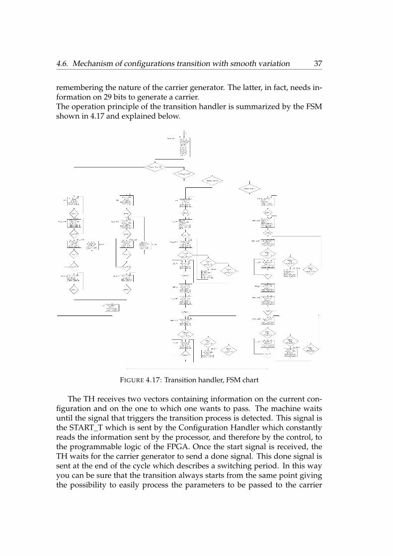
remembering the nature of the carrier generator. The latter, in fact, needs in-formation on 29 bits to generate a carrier.The operation principle of the transition handler is summarized by the FSMshown in 4.17 and explained below.
FIGURE 4.17: Transition handler, FSM chart
The TH receives two vectors containing information on the current con-figuration and on the one to which one wants to pass. The machine waitsuntil the signal that triggers the transition process is detected. This signal isthe START_T which is sent by the Configuration Handler which constantlyreads the information sent by the processor, and therefore by the control, tothe programmable logic of the FPGA. Once the start signal is received, theTH waits for the carrier generator to send a done signal. This done signal issent at the end of the cycle which describes a switching period. In this wayyou can be sure that the transition always starts from the same point givingthe possibility to easily process the parameters to be passed to the carrier
38 Chapter 4. PWM signals generation
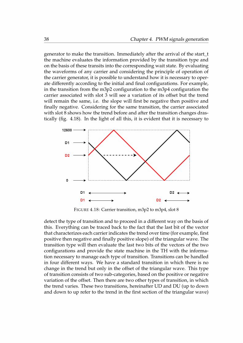
generator to make the transition. Immediately after the arrival of the start_tthe machine evaluates the information provided by the transition type andon the basis of these transits into the corresponding wait state. By evaluatingthe waveforms of any carrier and considering the principle of operation ofthe carrier generator, it is possible to understand how it is necessary to oper-ate differently according to the initial and final configurations. For example,in the transition from the m3p2 configuration to the m3p4 configuration thecarrier associated with slot 3 will see a variation of its offset but the trendwill remain the same, i.e. the slope will first be negative then positive andfinally negative. Considering for the same transition, the carrier associatedwith slot 8 shows how the trend before and after the transition changes dras-tically (fig. 4.18). In the light of all this, it is evident that it is necessary to
FIGURE 4.18: Carrier transition, m3p2 to m3p4, slot 8
detect the type of transition and to proceed in a different way on the basis ofthis. Everything can be traced back to the fact that the last bit of the vectorthat characterizes each carrier indicates the trend over time (for example, firstpositive then negative and finally positive slope) of the triangular wave. Thetransition type will then evaluate the last two bits of the vectors of the twoconfigurations and provide the state machine in the TH with the informa-tion necessary to manage each type of transition. Transitions can be handledin four different ways. We have a standard transition in which there is nochange in the trend but only in the offset of the triangular wave. This typeof transition consists of two sub-categories, based on the positive or negativevariation of the offset. Then there are two other types of transition, in whichthe trend varies. These two transitions, hereinafter UD and DU (up to downand down to up refer to the trend in the first section of the triangular wave)
4.7. Simulation results 39
are managed in two main processes. In practice, it is as if the single transi-tion were divided into two smaller transitions, each of which is managed asa standard transition. Blocks dedicated to each type of transition have thetask of detecting the moment in which the trend of the triangular wave mustbe reversed by generating control signals that will make the state machineevolve appropriately passing from the first standard transition cycle to thesecond. Referring to the transition m3p2 to m3p4 and once again consid-ering the carrier associated with slot 8, we are referring to the states DUR,DUR_LOAD1, DUR_WAIT1, DUR_W1, EN_M5_2 and RST_M5 for the firstpart of the transition in which the initial trend is maintained . In this waythe carrier maintains a down-up-down trend in which the offset graduallyvaries period after period. Once the offset has been varied up to the pointwhere it is necessary to reverse the trend, the FSM will evolve into the statesDUR_LOAD2, DUR_WAIT2, DUR_W2, EN_M5_4 and finally RST_M.
4.7 Simulation results
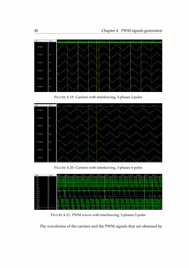
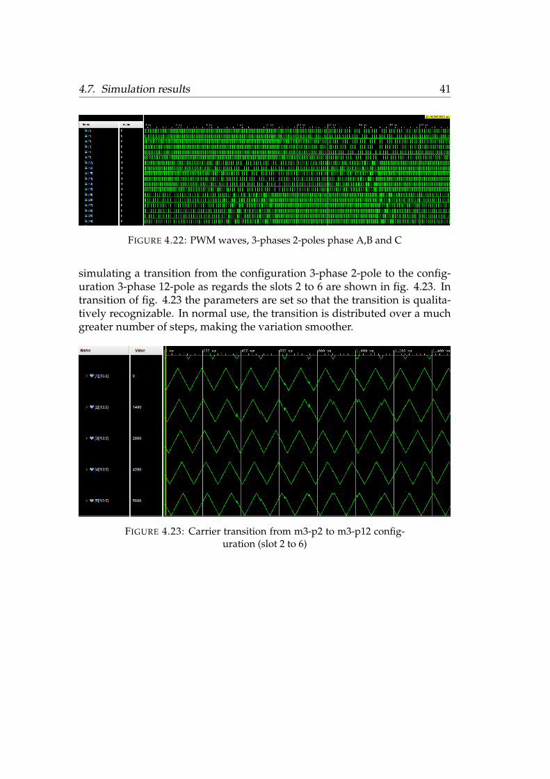
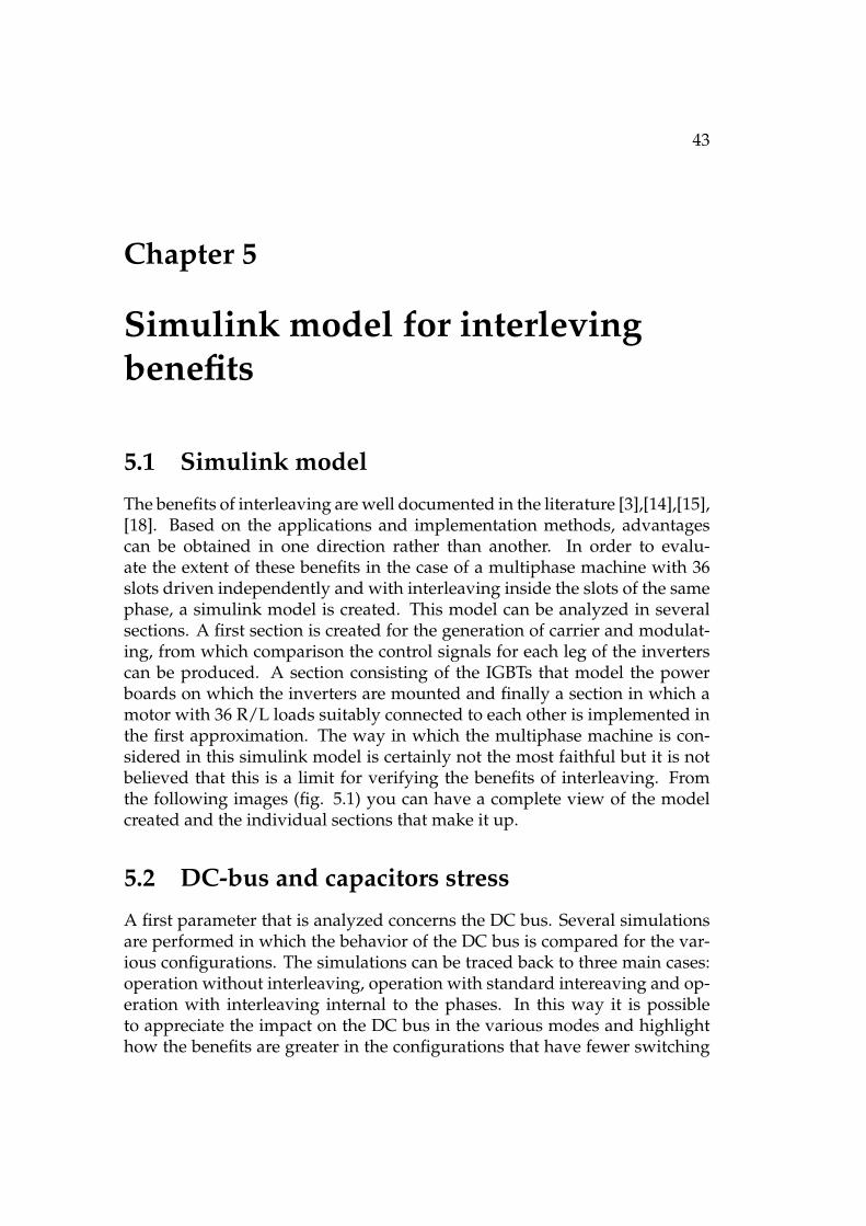
The carriers produced in the PWM section are displayed using the ’analogwaveform’ setting offered by the simulator in Vivado. In this way the nu-merical information that constitutes the carrier is reconstructed giving thepossibility to have a comparison with the trend of an equivalent analog trian-gular wave. Below are two figures from two different simulation both relatedto the carriers generated ad associated to the slots 1 to 6. Fig. 4.19 containsthe carrier generated while the machine is running in the 3-phases 2-polesconfiguration. It is possibile to have a qualitatively feedback on the grad-ual phase-shift between the carriers associated the phase A. A more compliteview is offered in fig. 4.20. This latter represents the carriers associated toslots 1 to 7 when the MPM is made run in the 3-phases 6-poles configuration.It’s possible to see that the behavior obtained is the one described in 4.3.1.The first six carriers are related to the phase A,B and C and the are shiftedand distributed over an entire switching period. Finally, from the seventhcarrier the behavior is repeated as for the previous carriers. In fig. 4.21 it ispossible to observe the simulation result as regards the output of the PWMsection for the configuration 3-phases 2-poles. In particular it’s plotted thebehaviour of phases A,B and C zooming in to appreciate the implementa-tion of the interleaving inside each phase. Fig. 4.21 is obtained from a longer(over 20ms) simulation that allows to verify the correct operation of the PWMsection. Fig. 4.22 offers the possibility to check the phase shit between phaseA,B and C while the machine runs in the 3-phase 2-poles configuration.
40 Chapter 4. PWM signals generation
FIGURE 4.19: Carriers with interleaving, 3-phases 2-poles
FIGURE 4.20: Carriers with interleaving, 3-phases 6-poles
FIGURE 4.21: PWM waves with interleaving, 3-phases 2-poles
The waveforms of the carriers and the PWM signals that are obtained by
4.7. Simulation results 41
FIGURE 4.22: PWM waves, 3-phases 2-poles phase A,B and C
simulating a transition from the configuration 3-phase 2-pole to the config-uration 3-phase 12-pole as regards the slots 2 to 6 are shown in fig. 4.23. Intransition of fig. 4.23 the parameters are set so that the transition is qualita-tively recognizable. In normal use, the transition is distributed over a muchgreater number of steps, making the variation smoother.
FIGURE 4.23: Carrier transition from m3-p2 to m3-p12 config-uration (slot 2 to 6)

43
Chapter 5
Simulink model for interlevingbenefits
5.1 Simulink model
The benefits of interleaving are well documented in the literature [3],[14],[15],[18]. Based on the applications and implementation methods, advantagescan be obtained in one direction rather than another. In order to evalu-ate the extent of these benefits in the case of a multiphase machine with 36slots driven independently and with interleaving inside the slots of the samephase, a simulink model is created. This model can be analyzed in severalsections. A first section is created for the generation of carrier and modulat-ing, from which comparison the control signals for each leg of the inverterscan be produced. A section consisting of the IGBTs that model the powerboards on which the inverters are mounted and finally a section in which amotor with 36 R/L loads suitably connected to each other is implemented inthe first approximation. The way in which the multiphase machine is con-sidered in this simulink model is certainly not the most faithful but it is notbelieved that this is a limit for verifying the benefits of interleaving. Fromthe following images (fig. 5.1) you can have a complete view of the modelcreated and the individual sections that make it up.
5.2 DC-bus and capacitors stress
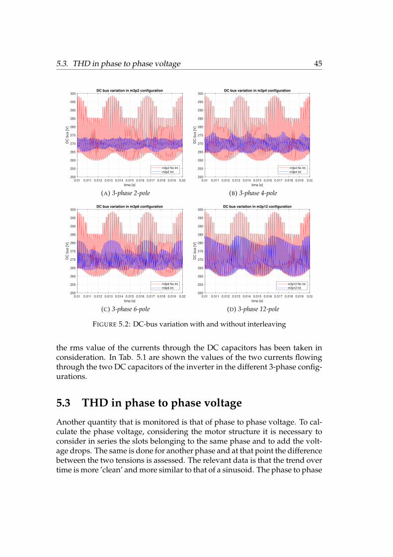
A first parameter that is analyzed concerns the DC bus. Several simulationsare performed in which the behavior of the DC bus is compared for the var-ious configurations. The simulations can be traced back to three main cases:operation without interleaving, operation with standard intereaving and op-eration with interleaving internal to the phases. In this way it is possibleto appreciate the impact on the DC bus in the various modes and highlighthow the benefits are greater in the configurations that have fewer switching
44 Chapter 5. Simulink model for interleving benefits
(A) Overall view (B) DC bus
(C) PWM section (D) R/L load
FIGURE 5.1: Simulink model for interleaving benefits verifica-tion
at the same time. The following graphs (5.2) show how, for each configu-ration, passing from a drive of the IGBTs without interleaving to one withinterleaving there is a more contained variation of the voltage on the DC bus.A configuration with a greater number of different carriers will be character-ized by multiple switching at different instants, thus maximizing the effectsof interleaving. This means that the improvement in the performance of theDC bus that is found in the same configuration by introducing or not intro-ducing interleaving can be found when the configuration changes. A usefulcomparison can be that between the m3p2, m3p4, m3p6 and m3p12 configu-rations (fig. 5.2).Another aspect concerns DC capacitors. It can be seen that these are morestressed in the case of PWM without interleaving. The current flowing throughthem is assessed and from the simulations it is seen how evident improve-ments are obtained thanks to the use of interleaving. The amplitude of thecurrent that flows through them is lower. Below are the simulation graphsfor a comparison, of the m3p2 configuration, with and without interleaving(fig. 5.3), and two graphics for comparing the current through DC bus capac-itor 1 (100nF) and DC bus capacitor 2 (25µF) in all the 3-phase configurations(figures 5.4 a and b respectively).
This improvement allows for more relaxed specifications on the choice ofDC capacitors. In order to have more evidence of the interleaving benefits
5.3. THD in phase to phase voltage 45
0.01 0.011 0.012 0.013 0.014 0.015 0.016 0.017 0.018 0.019 0.02
time [s]
250
255
260
265
270
275
280
285
290
295
300
DC
bu
s [
V]
DC bus variation in m3p2 configuration
m3p2 No Int.
m3p2 Int.
(A) 3-phase 2-pole
0.01 0.011 0.012 0.013 0.014 0.015 0.016 0.017 0.018 0.019 0.02
time [s]
250
255
260
265
270
275
280
285
290
295
300
DC
bu
s [
V]
DC bus variation in m3p4 configuration
m3p4 No Int.
m3p4 Int.
(B) 3-phase 4-pole
0.01 0.011 0.012 0.013 0.014 0.015 0.016 0.017 0.018 0.019 0.02
time [s]
250
255
260
265
270
275
280
285
290
295
300
DC
bu
s [
V]
DC bus variation in m3p6 configuration
m3p6 No Int.
m3p6 Int.
(C) 3-phase 6-pole
0.01 0.011 0.012 0.013 0.014 0.015 0.016 0.017 0.018 0.019 0.02
time [s]
250
255
260
265
270
275
280
285
290
295
300
DC
bu
s [
V]
DC bus variation in m3p12 configuration
m3p12 No Int.
m3p12 Int.
(D) 3-phase 12-pole
FIGURE 5.2: DC-bus variation with and without interleaving
the rms value of the currents through the DC capacitors has been taken inconsideration. In Tab. 5.1 are shown the values of the two currents flowingthrough the two DC capacitors of the inverter in the different 3-phase config-urations.
5.3 THD in phase to phase voltage
Another quantity that is monitored is that of phase to phase voltage. To cal-culate the phase voltage, considering the motor structure it is necessary toconsider in series the slots belonging to the same phase and to add the volt-age drops. The same is done for another phase and at that point the differencebetween the two tensions is assessed. The relevant data is that the trend overtime is more ’clean’ and more similar to that of a sinusoid. The phase to phase
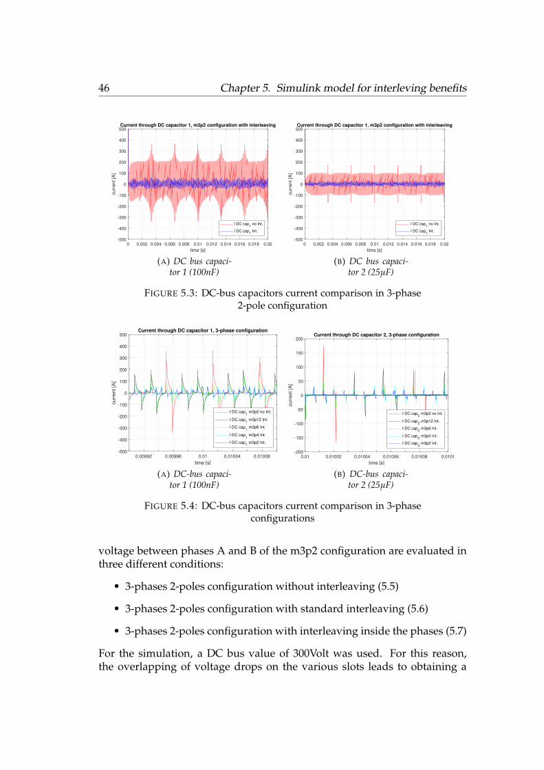
46 Chapter 5. Simulink model for interleving benefits
0 0.002 0.004 0.006 0.008 0.01 0.012 0.014 0.016 0.018 0.02
time [s]
-500
-400
-300
-200
-100
0
100
200
300
400
500
curr
ent [A
]
Current through DC capacitor 1, m3p2 configuration with interleaving
I DC cap1 no Int.
I DC cap1 Int.
(A) DC bus capaci-tor 1 (100nF)
0 0.002 0.004 0.006 0.008 0.01 0.012 0.014 0.016 0.018 0.02
time [s]
-500
-400
-300
-200
-100
0
100
200
300
400
500
curr
ent [A
]
Current through DC capacitor 1, m3p2 configuration with interleaving
I DC cap1 no Int.
I DC cap1 Int.
(B) DC bus capaci-tor 2 (25µF)
FIGURE 5.3: DC-bus capacitors current comparison in 3-phase2-pole configuration
0.00992 0.00996 0.01 0.01004 0.01008
time [s]
-500
-400
-300
-200
-100
0
100
200
300
400
500
cu
rre
nt
[A]
Current through DC capacitor 1, 3-phase configuration
I DC cap1 m3p2 no Int.
I DC cap1 m3p12 Int.
I DC cap1 m3p6 Int.
I DC cap1 m3p4 Int.
I DC cap1 m3p2 Int.
(A) DC-bus capaci-tor 1 (100nF)
0.01 0.01002 0.01004 0.01006 0.01008 0.0101
time [s]
-200
-150
-100
-50
0
50
100
150
200
cu
rre
nt
[A]
Current through DC capacitor 2, 3-phase configuration
I DC cap2 m3p2 no Int.
I DC cap2 m3p12 Int.
I DC cap2 m3p6 Int.
I DC cap2 m3p4 Int.
I DC cap2 m3p2 Int.
(B) DC-bus capaci-tor 2 (25µF)
FIGURE 5.4: DC-bus capacitors current comparison in 3-phaseconfigurations
voltage between phases A and B of the m3p2 configuration are evaluated inthree different conditions:
• 3-phases 2-poles configuration without interleaving (5.5)
• 3-phases 2-poles configuration with standard interleaving (5.6)
• 3-phases 2-poles configuration with interleaving inside the phases (5.7)
For the simulation, a DC bus value of 300Volt was used. For this reason,the overlapping of voltage drops on the various slots leads to obtaining a
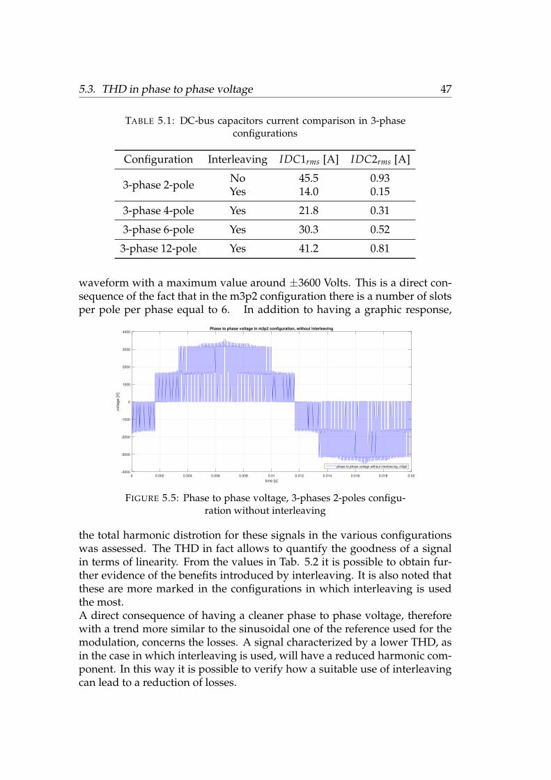
5.3. THD in phase to phase voltage 47
TABLE 5.1: DC-bus capacitors current comparison in 3-phaseconfigurations
Configuration Interleaving IDC1rms [A] IDC2rms [A]
3-phase 2-pole No 45.5 0.93Yes 14.0 0.15
3-phase 4-pole Yes 21.8 0.31
3-phase 6-pole Yes 30.3 0.52
3-phase 12-pole Yes 41.2 0.81
waveform with a maximum value around ±3600 Volts. This is a direct con-sequence of the fact that in the m3p2 configuration there is a number of slotsper pole per phase equal to 6. In addition to having a graphic response,
0 0.002 0.004 0.006 0.008 0.01 0.012 0.014 0.016 0.018 0.02
time [s]
-4000
-3000
-2000
-1000
0
1000
2000
3000
4000
vo
lta
ge
[V
]
Phase to phase voltage in m3p2 configuration, without interleaving
phase to phase voltage without interleaving, m3p2
FIGURE 5.5: Phase to phase voltage, 3-phases 2-poles configu-ration without interleaving
the total harmonic distrotion for these signals in the various configurationswas assessed. The THD in fact allows to quantify the goodness of a signalin terms of linearity. From the values in Tab. 5.2 it is possible to obtain fur-ther evidence of the benefits introduced by interleaving. It is also noted thatthese are more marked in the configurations in which interleaving is usedthe most.A direct consequence of having a cleaner phase to phase voltage, thereforewith a trend more similar to the sinusoidal one of the reference used for themodulation, concerns the losses. A signal characterized by a lower THD, asin the case in which interleaving is used, will have a reduced harmonic com-ponent. In this way it is possible to verify how a suitable use of interleavingcan lead to a reduction of losses.
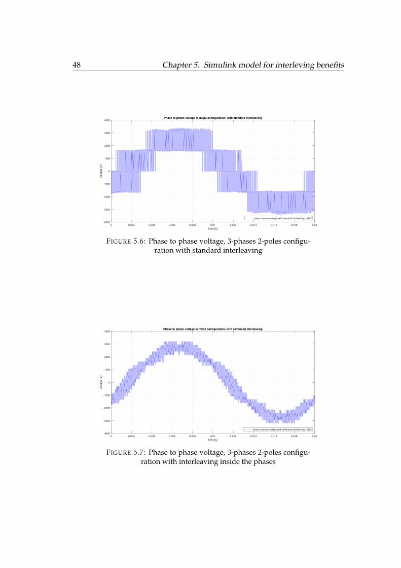
48 Chapter 5. Simulink model for interleving benefits
0 0.002 0.004 0.006 0.008 0.01 0.012 0.014 0.016 0.018 0.02
time [s]
-4000
-3000
-2000
-1000
0
1000
2000
3000
4000
vo
lta
ge
[V
]
Phase to phase voltage in m3p2 configuration, with standard interleaving
phase to phase voltage with standard interleaving, m3p2
FIGURE 5.6: Phase to phase voltage, 3-phases 2-poles configu-ration with standard interleaving
0 0.002 0.004 0.006 0.008 0.01 0.012 0.014 0.016 0.018 0.02
time [s]
-4000
-3000
-2000
-1000
0
1000
2000
3000
4000
vo
lta
ge
[V
]
Phase to phase voltage in m3p2 configuration, with advanced interleaving
phase to phase voltage with advanced interleaving, m3p2
FIGURE 5.7: Phase to phase voltage, 3-phases 2-poles configu-ration with interleaving inside the phases
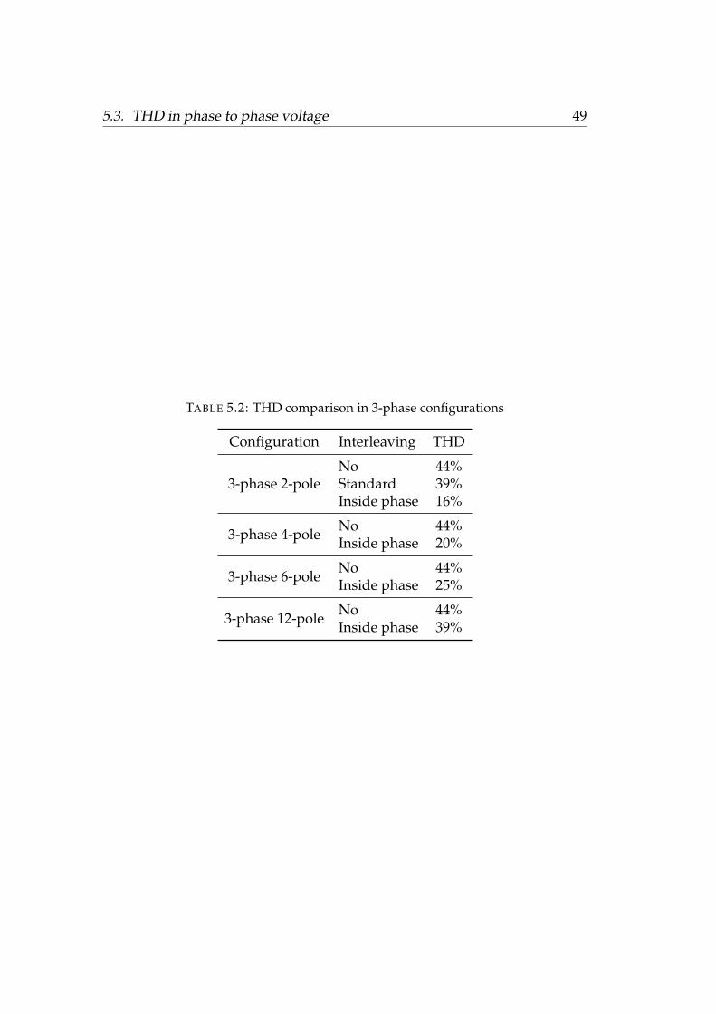
5.3. THD in phase to phase voltage 49
TABLE 5.2: THD comparison in 3-phase configurations
Configuration Interleaving THD
3-phase 2-poleNo 44%Standard 39%Inside phase 16%
3-phase 4-pole No 44%Inside phase 20%
3-phase 6-pole No 44%Inside phase 25%
3-phase 12-pole No 44%Inside phase 39%

51
Chapter 6
Measurements and results
6.1 A/D conversion Testbench
A tailor-made testbench was created to test the correct functioning of theADC and verify the correct acquisition of the samples on the FPGA. Thesetup involves the use of:
• A signal generator
• AD9249 EVM
• ZYNQ ZC702
• PC
The output 1 of a signal generator was connected to the input of channel 1of the conversion board. To make this connection it was necessary to usededicated SMA to BNC adapters. The same type of connection was madebetween output 2 of the signal generator and the ADC input dedicated tothe clock. AD9249 outputs are available on a male FMC connector. Thisconnector was then connected to one of the female FMC connectors on theFPGA. The zynq ZC702 was then connected to a terminal via a micro USBconnector. The testbench just described expect that a signal is supplied to theconverter input to be sampled. Sampling is scanned by the frequency of theclock signal which is supplied externally via the signal generator. The ADCsamples and sends the data to the FPGA which constantly acquires them. TheFPGA constantly acquires each sample through the mechanism illustrated in3.2 and if no other operation is required at the next clock edge, the sampleis overwritten. When desired, externally the FPGA can be communicatedto start saving the samples in a register file. As soon as it comes the RF iscompletely filled, the RF will send the samples one at a time to the processor.At that point the samples are sent via UART on the terminal. Once printedon the terminal, the samples are collected and processed. The ADC sends thesamples in twos complement notation. After collecting them, the samplesare manipulated in order to reconstruct the original information. Once this is
52 Chapter 6. Measurements and results
done, the obtained samples are plotted in Matlab. The RF instanced in VHDLhas a capacity of 30 samples. Consequently it will be necessary to vary thefrequency of the signal that enables the shift-register of which we discussedin 3.2. This frequency is varied according to the signal being sampled inorder to acquire one or more periods. In fig. 6.1 and 6.2 it is possible toobserve the curve obtained by plotting the 30 samples acquired in the caseof 1 and 2 observation periods respectively. The amplitude of the sinusoidalsignal was kept in a range reasonably lower than the maximum expected inthe converter datasheet [1].
5 10 15 20 25 30
Sample #
0
2000
4000
6000
8000
10000
12000
14000
16000
AD
C s
am
ple
s (
14
bits r
an
ge
)
Ideal wave
ADC samples
FIGURE 6.1: ADC samples - one period
6.2 PWM square waves analysis
The code for the PWM section was initially simulated in Vivado. As reportedin 4.7 it was possible to verify that the structure created was able to correctlygenerate the output of the pwm section. In particular, the generation of car-riers based on the configuration was verified, paying attention to the phaseshift introduced to implement interleaving. Once a generic 50Hz sinusoidalreference with peak to peak amplitude corresponding to the entire carrierrange was implemented and tested, it was possible to evaluate the wave-forms obtained by the comparison between carrier and modulating. Finally,the behavior of the various carriers was simulated to verify correct operation
6.2. PWM square waves analysis 53
5 10 15 20 25 30
Sample #
0
2000
4000
6000
8000
10000
12000
14000
16000A
DC
sa
mp
les (
14
bits r
an
ge
)Ideal wave
ADC samples
FIGURE 6.2: ADC samples - two period
during the configuration transition. Once the correct simulation operationwas verified, it was possible to synthesize the hardware described in VHDLon the FPGA and experimentally evaluate its operation. For the acquisitionof measurements on the waveforms, an oscilloscope and a logic state ana-lyzer with 16 digital input channels were used. The first allowed to have abetter resolution but offering the possibility to display only 4 channels at atime. With the logic state analyzer, it was possible to simultaneously display16 signals thus allowing to evaluate a reasonable number of outputs of thePWM section and verify their correct operation.
6.2.1 Verification of PWM outputs
The nine predisposed configurations have been fully verified. Below are thewaves acquired through the logic state analyzer of some of the configurationscapable of offering feedback of the modulation carried out with particular at-tention to the behavior due to interleaving. The m3p2 configuration is char-acterized by a qs (slot per pole per phase) equal to 6. In figure 6.3 the squarewaves associated with phase A are shown. It can be seen that by introducinga phase shift of 20 degrees between the carriers , the square waves associatedwith the same phase and therefore with the same reference, are out of phaseas expected for the interleaving used.
54 Chapter 6. Measurements and results
FIGURE 6.3: PWM signals (phase A, 3-phase 2-poles)
Figure 6.4 shows the waves associated with phases A, B and C in the m3p4configuration. This configuration is characterized by a qs equal to 3. Theperiod observed is equal to 30ms. In such a way it’s possible to recognizethe periodicity of 20ms (corresponding to a 50Hz signal) of the modulatedsignal. It is possible to recognize the three phases considering that each isout of phase of 120 degrees with respect the others. It is also possible toappreciate qualitatively at each phase the internal shift due to interleaving .
FIGURE 6.4: PWM signals (phase A B and C, 3-phase 4-poles)
The configurations characterized by m = 6 and the configuration m18p2are made as several three-phase systems suitably phase-shifted. In fig. 6.5 itis possible to observe the waveforms associated with phases A1,A2,B1,B2,C1
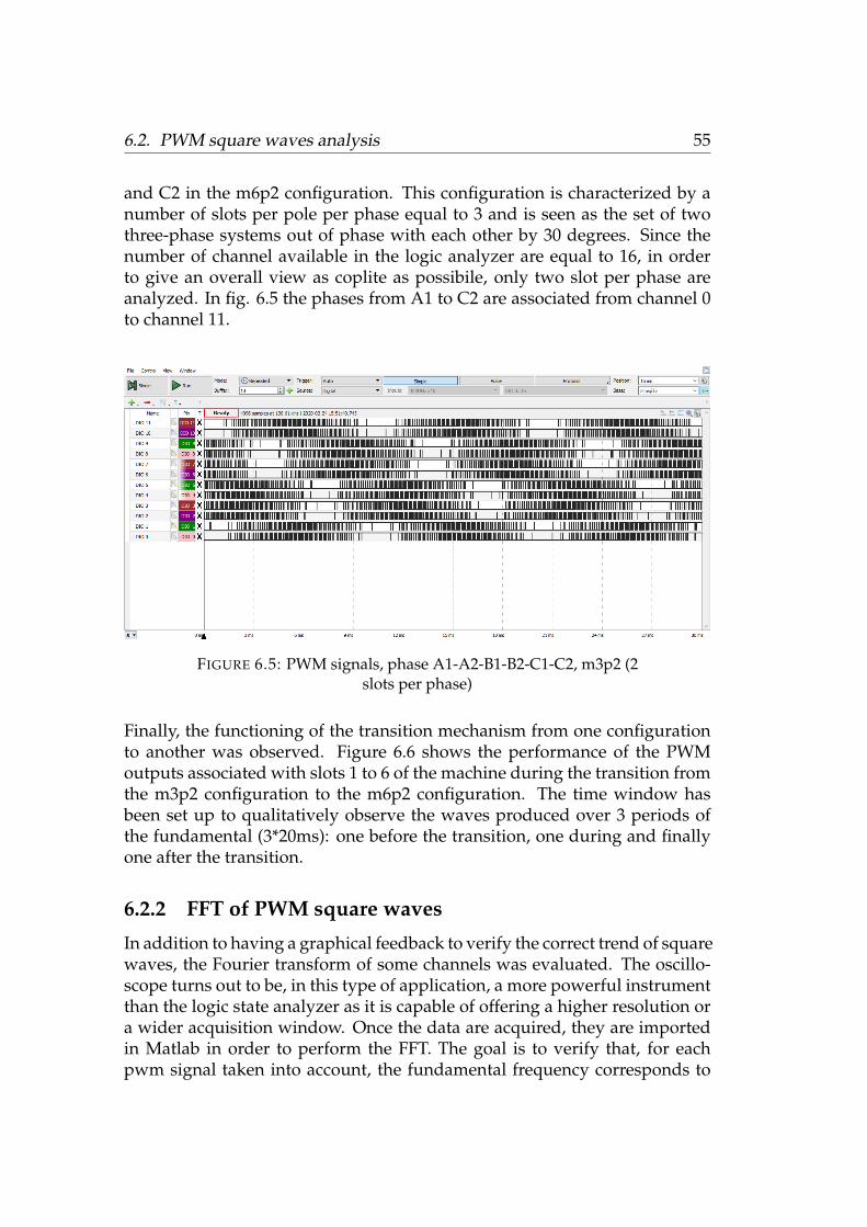
6.2. PWM square waves analysis 55
and C2 in the m6p2 configuration. This configuration is characterized by anumber of slots per pole per phase equal to 3 and is seen as the set of twothree-phase systems out of phase with each other by 30 degrees. Since thenumber of channel available in the logic analyzer are equal to 16, in orderto give an overall view as coplite as possibile, only two slot per phase areanalyzed. In fig. 6.5 the phases from A1 to C2 are associated from channel 0to channel 11.
FIGURE 6.5: PWM signals, phase A1-A2-B1-B2-C1-C2, m3p2 (2slots per phase)
Finally, the functioning of the transition mechanism from one configurationto another was observed. Figure 6.6 shows the performance of the PWMoutputs associated with slots 1 to 6 of the machine during the transition fromthe m3p2 configuration to the m6p2 configuration. The time window hasbeen set up to qualitatively observe the waves produced over 3 periods ofthe fundamental (3*20ms): one before the transition, one during and finallyone after the transition.
6.2.2 FFT of PWM square waves
In addition to having a graphical feedback to verify the correct trend of squarewaves, the Fourier transform of some channels was evaluated. The oscillo-scope turns out to be, in this type of application, a more powerful instrumentthan the logic state analyzer as it is capable of offering a higher resolution ora wider acquisition window. Once the data are acquired, they are importedin Matlab in order to perform the FFT. The goal is to verify that, for eachpwm signal taken into account, the fundamental frequency corresponds to
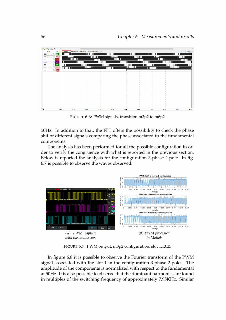
56 Chapter 6. Measurements and results
FIGURE 6.6: PWM signals, transition m3p2 to m6p2
50Hz. In addition to that, the FFT offers the possibility to check the phaseshif of different signals comparing the phase associated to the fundamentalcomponents.
The analysis has been performed for all the possible configuration in or-der to verify the congruence with what is reported in the previous section.Below is reported the analysis for the configuration 3-phase 2-pole. In fig.6.7 is possible to observe the waves observed.
(A) PWM capturewith the oscilloscope
0 0.002 0.004 0.006 0.008 0.01 0.012 0.014 0.016 0.018 0.02
time [s]
-2
0
2
am
plit
ud
e [
V]
PWM slot 1 in m=3 p=2 configuration
0 0.002 0.004 0.006 0.008 0.01 0.012 0.014 0.016 0.018 0.02
time [s]
-2
0
2
am
plit
ud
e [
V]
PWM slot 13 in m=3 p=2 configuration
0 0.002 0.004 0.006 0.008 0.01 0.012 0.014 0.016 0.018 0.02
time [s]
-2
0
2
am
plit
ud
e [
V]
PWM slot 25 in m=3 p=2 configuration
(B) PWM processedin Matlab
FIGURE 6.7: PWM output, m3p2 configuration, slot 1,13,25
In figure 6.8 it is possible to observe the Fourier transform of the PWMsignal associated with the slot 1 in the configuration 3-phase 2-poles. Theamplitude of the components is normalized with respect to the fundamentalat 50Hz. It is also possible to observe that the dominant harmonics are foundin multiples of the switching frequency of approximately 7.95KHz. Similar
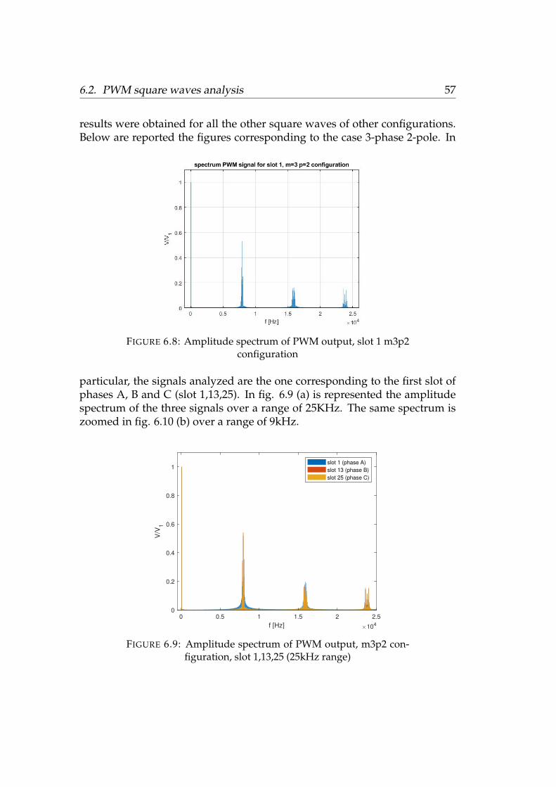
6.2. PWM square waves analysis 57
results were obtained for all the other square waves of other configurations.Below are reported the figures corresponding to the case 3-phase 2-pole. In
FIGURE 6.8: Amplitude spectrum of PWM output, slot 1 m3p2configuration
particular, the signals analyzed are the one corresponding to the first slot ofphases A, B and C (slot 1,13,25). In fig. 6.9 (a) is represented the amplitudespectrum of the three signals over a range of 25KHz. The same spectrum iszoomed in fig. 6.10 (b) over a range of 9kHz.
0 0.5 1 1.5 2 2.5
f [Hz] 104
0
0.2
0.4
0.6
0.8
1
V/V
1
slot 1 (phase A)
slot 13 (phase B)
slot 25 (phase C)
FIGURE 6.9: Amplitude spectrum of PWM output, m3p2 con-figuration, slot 1,13,25 (25kHz range)
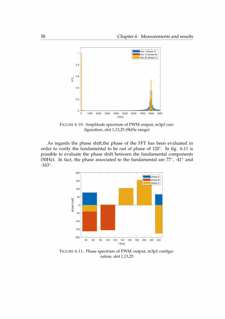
58 Chapter 6. Measurements and results
0 1000 2000 3000 4000 5000 6000 7000 8000 9000
f [Hz]
0
0.2
0.4
0.6
0.8
1
V/V
1
slot 1 (phase A)
slot 13 (phase B)
slot 25 (phase C)
FIGURE 6.10: Amplitude spectrum of PWM output, m3p2 con-figuration, slot 1,13,25 (9kHz range)
As regards the phase shift,the phase of the FFT has been evaluated inorder to verify the fundamental to be out of phase of 120◦. In fig. 6.11 ispossible to evaluate the phase shift between the fundamental components(50Hz). In fact, the phase associated to the fundamental are 77◦, -41◦ and-163◦.
40 60 80 100 120 140 160 180 200 220 240
f [Hz]
-200
-150
-100
-50
0
50
100
150
200
ph
ase
[ra
d]
phase A
phase B
phase C
FIGURE 6.11: Phase spectrum of PWM output, m3p2 configu-ration, slot 1,13,25
59
Chapter 7
Conclusions
The work here presented described the implementation on FPGA of a PulseWidth Modulation integrating the interleaving technique and of a systemable to handle the communication between FPGA and ADCs. As for thePWM, the implemented structure is characterized by an high level of flexi-bility. This flexibility is mainly related to the capability of online changingof the number of pole-pairs as well as the number of phases. This aspect isfundamental to meet specifications imposed by the configuration of the ma-chine under study. The two structures implemented have been simulatedand tested with dedicated testbench. At the end of the work, a Matlab-Simulink model is created (which represents the machine under study as afirst approximation) in order to have concrete evidence of the improvementsobtained. Thanks to the model created, it was possible to verify how the im-provements are more consistent in the configurations that maximize the useof interleaving.
7.1 Improvement obtained
The improvements obtained are due to the implemented modulation tech-nique, with reference to the advantages brought by the use of interleaving.This technique perfectly matched the structure of the motor, leading to a fur-ther step or rather the implementation of interleaving within the phases. Theimprovements obtained, documented in chapter 5, refer to the stress on theDC-bus and on the decoupling and bypass capacitors in the board with theinverters. Equally important results have been obtained with regards to thegoodness of the phase-to-phase voltage, obtaining a remarkable feedback ofthe impact of interleaving on the Total Harmonic Distortion of this voltage.The latter result translates into an improvement in the overall efficiency ofthe system.

60 Chapter 7. Conclusions
7.2 Future works
Future work will focus on perfecting the modulation technique to make thesystem able to deal with the fault of one or more slots. The algorithm mayrefer to the one already implemented for the management of transitions fromone configuration to another. A further aspect to work on in the future will bethat of the complication of the architecture implemented to obtain the man-agement of the configuration characterized by a non-integer number of slotsper pole per phase, leading to an even more flexible structure.
61
Bibliography
[1] Analog Devices, AD9249 - Data Sheet. URL: ❤tt♣s✿✴✴✇✇✇✳❛♥❛❧♦❣✳❝♦♠✴♠❡❞✐❛✴❡♥✴t❡❝❤♥✐❝❛❧✲❞♦❝✉♠❡♥t❛t✐♦♥✴❞❛t❛✲s❤❡❡ts✴❆❉✾✷✹✾✳♣❞❢.
[2] Konstantina Bitsi, Oskar Wallmark, and Sjoerd Bosga. “An InductionMachine with Wound Independently-Controlled Stator Coils”. en. In:2019 22nd International Conference on Electrical Machines and Systems (ICEMS).Harbin, China: IEEE, Aug. 2019, pp. 1–5. ISBN: 978-1-72813-398-0. DOI:✶✵✳✶✶✵✾✴■❈❊▼❙✳✷✵✶✾✳✽✾✷✶✼✼✾. URL: ❤tt♣s✿✴✴✐❡❡❡①♣❧♦r❡✳✐❡❡❡✳♦r❣✴❞♦❝✉♠❡♥t✴✽✾✷✶✼✼✾✴.
[3] Gabriel J. Capella et al. “Enhanced Phase-Shifted PWM Carrier Dispo-sition for Interleaved Voltage-Source Inverters”. en. In: IEEE Transac-tions on Power Electronics 30.3 (Mar. 2015), pp. 1121–1125. ISSN: 0885-8993, 1941-0107. DOI: ✶✵✳✶✶✵✾✴❚P❊▲✳✷✵✶✹✳✷✸✸✽✸✺✼. URL: ❤tt♣✿✴✴✐❡❡❡①♣❧♦r❡✳✐❡❡❡✳♦r❣✴❞♦❝✉♠❡♥t✴✻✽✻✵✷✺✾✴.
[4] Gurakuq Dajaku and Dieter Gerling. “Low costs and high efficiencyasynchronous machine with stator cage winding”. en. In: 2014 IEEE In-ternational Electric Vehicle Conference (IEVC). Florence: IEEE, Dec. 2014,pp. 1–6. ISBN: 978-1-4799-6075-0. DOI: ✶✵✳✶✶✵✾✴■❊❱❈✳✷✵✶✹✳✼✵✺✻✵✽✸.URL: ❤tt♣s✿✴✴✐❡❡❡①♣❧♦r❡✳✐❡❡❡✳♦r❣✴❞♦❝✉♠❡♥t✴✼✵✺✻✵✽✸✴.
[5] Shaahin Filizadeh. Electric Machines and Drives: Principles, Control, Mod-eling, and Simulation. CRC Press, 2017.
[6] D. Grahame Holmes and T. A. Lipo. Pulse width modulation for powerconverters: principles and practice. en. Hoboken, NJ: John Wiley, 2003.ISBN: 978-0-471-20814-3.
[7] Hsung-Hao Hsu and Ying-Yu Tzou. “FPGA control and implementa-tion of a multiphase-interleaved PWM inverter for a segmented PMSM”.en. In: 2015 IEEE 11th International Conference on Power Electronics andDrive Systems. Sydney, Australia: IEEE, June 2015, pp. 224–230. ISBN:978-1-4799-4402-6. DOI: ✶✵ ✳ ✶✶✵✾ ✴ P❊❉❙ ✳ ✷✵✶✺ ✳ ✼✷✵✸✹✶✵. URL: ❤tt♣ ✿✴✴✐❡❡❡①♣❧♦r❡✳✐❡❡❡✳♦r❣✴❞♦❝✉♠❡♥t✴✼✷✵✸✹✶✵✴.
[8] E. A. Klingshirn. “High Phase Order Induction Motors - Part II-ExperimentalResults”. In: IEEE Transactions on Power Apparatus and Systems, vol. PAS-102, no. 1, pp. 54-59 ().
62 Bibliography
[9] E. Levi. “Multiphase Electric Machines for Variable-Speed Applications”.en. In: IEEE Transactions on Industrial Electronics 55.5 (May 2008), pp. 1893–1909. ISSN: 0278-0046. DOI: ✶✵✳✶✶✵✾✴❚■❊✳✷✵✵✽✳✾✶✽✹✽✽. URL: ❤tt♣✿✴✴✐❡❡❡①♣❧♦r❡✳✐❡❡❡✳♦r❣✴❞♦❝✉♠❡♥t✴✹✹✺✹✹✹✻✴.
[10] E. Levi et al. “Multiphase induction motor drives – a technology sta-tus review”. en. In: IET Electric Power Applications 1.4 (2007), p. 489.ISSN: 17518660. DOI: ✶✵ ✳ ✶✵✹✾ ✴ ✐❡t ✲ ❡♣❛ ✿ ✷✵✵✻✵✸✹✷. URL: ❤tt♣s ✿ ✴ ✴❞✐❣✐t❛❧✲ ❧✐❜r❛r②✳t❤❡✐❡t✳♦r❣✴❝♦♥t❡♥t✴❥♦✉r♥❛❧s✴✶✵✳✶✵✹✾✴✐❡t✲
❡♣❛❴✷✵✵✻✵✸✹✷.
[11] R. H. Nelson and P. C. Krause. “Induction Machine Analysis for Ar-bitrary Displacement Between Multiple Winding Sets”. In: IEEE Trans-actions on Power Apparatus and Systems, vol. PAS-93, no. 3, pp. 841-848().
[12] L. Peretti and G. Zanuso. “Technology aspects and analytical mod-elling of multi-phase synchronous and induction machines”. Sept. 2019.
[13] A. Tessarolo. “Modeling and analysis of multiphase electric machinesfor high power applications”. PhD thesis. University of Padova, Schoolof Industrial Engineering, program of Electrotechnical Engineering, 2011.
[14] M Varun et al. “A new hybrid PWM for two parallel connected inter-leaved two-level inverter to reduce output current ripple”. en. In: 2017IEEE 7th International Conference on Power and Energy Systems (ICPES).Toronto, ON: IEEE, Nov. 2017, pp. 74–79. ISBN: 978-1-5386-2428-9 978-1-5386-2429-6. DOI: ✶✵✳✶✶✵✾✴■❈P❊❙❨❙✳✷✵✶✼✳✽✷✶✺✾✷✹. URL: ❤tt♣✿✴✴✐❡❡❡①♣❧♦r❡✳✐❡❡❡✳♦r❣✴❞♦❝✉♠❡♥t✴✽✷✶✺✾✷✹✴.
[15] Adrien Voldoire et al. “Analytical Calculation of DC-Link Current forN-Interleaved 3-Phase PWM Inverters Considering AC Current Rip-ple”. en. In: 2019 21st European Conference on Power Electronics and Ap-plications (EPE ’19 ECCE Europe). Genova, Italy: IEEE, Sept. 2019, P.1–P.10. ISBN: 978-90-75815-31-3. DOI: ✶✵✳✷✸✾✶✾✴❊P❊✳✷✵✶✾✳✽✾✶✺✶✽✸. URL:❤tt♣s✿✴✴✐❡❡❡①♣❧♦r❡✳✐❡❡❡✳♦r❣✴❞♦❝✉♠❡♥t✴✽✾✶✺✶✽✸✴.
[16] D. C. White and H. H. Woodson. Electromechanical Energy Conversion.John Wiley and Sons, 1959.
[17] Y. Wu and G. Falk Olson. “Analysis of a Phase-Pole Variable InductionMachine with a Multi-Harmonic Approach”. Jan. 2020.
[18] Saijun Zhang and Xiaoyan Yu. “A Unified Analytical Modeling of theInterleaved Pulse Width Modulation (PWM) DC–DC Converter andIts Applications”. en. In: IEEE Transactions on Power Electronics 28.11(Nov. 2013), pp. 5147–5158. ISSN: 0885-8993, 1941-0107. DOI: ✶✵✳✶✶✵✾✴❚P❊▲✳✷✵✶✸✳✷✷✹✺✻✽✸. URL: ❤tt♣✿✴✴✐❡❡❡①♣❧♦r❡✳✐❡❡❡✳♦r❣✴❞♦❝✉♠❡♥t✴✻✹✺✼✹✻✸✴.