Embed Size (px)
Citation preview
Materials Science and Engineering B71 (2000) 282–287
Polishing, chemical etching and thermal treatment effectson surface and electrical properties of
Er and Nd-doped GaSb substrates
J.L. Plaza a,*, P. Hidalgo b, B. Mendez b, J. Piqueras b, E. Dieguez a
a Departamento de Fısica de Materiales, Uni6ersidad Autonoma de Madrid 28049, Cantoblanco, Madrid, Spainb Departamento de Fısica de Materiales, Uni6ersidad Complutense 28040, Madrid, Spain
Abstract
In this work several changes induced by polishing, chemical etching and thermal treatment in the properties of Er- andNd-doped GaSb substrates with different doping levels grown by the vertical Bridgman method have been studied. The analysishas revealed the formation of precipitates at the highest doping levels for both Er- and Nd-doped GaSb. Cathodoluminescenceanalysis shows the reduction of the defect band induced by the rare earth (RE) elements. For high dopant concentrations theprecipitation phenomena reduce this effect. Thermal treatments have produced an enhancement of the p-type properties of thesamples. For a dopant density of 2×1019 cm−3 this effect is more pronounced. © 2000 Elsevier Science S.A. All rights reserved.
Keywords: Gallium antimonide; Rare earths; Thermal treatments
www.elsevier.com/locate/mseb
1. Introduction
Rare earth (RE) doped semiconductors are interest-ing materials due to their applications in optoelectron-ics. These systems present a temperature stableluminescence wavelength which is nearly independentof the semiconductor host. The interest in RE dopedsemiconductors is based on the fabrication of newelectroluminescence devices which can combine boththe luminescence of rare earth ions and the electronicproperties of semiconductors [1]. When RE elementsare introduced as trivalent ions in solids they exhibitatomic-like optical transitions due to the incomplete 4fshell which is shielded by the outermost filled 5s2 and5p6 orbitals. These intra-4f transitions are parity forbid-den in the free ion but are allowed when the RE ionsare embedded in solids due to the mixing of oppositeparity states produced by the local electric fields in thesolid host [2]. In addition the RE ions weakly interactwith the matrix and the wavelength of intra-4f shellemission is only slightly dependent on the host materialand the environmental temperature.
RE ions have been incorporated into III–V semicon-ductors by doping during the growth process [3–5]opening new possibilities to construct new optoelec-tronic devices. Er3+ is one of the most interesting REions due to the fact that its transition from 4I13/2 to the4I15/2 state appears at 1540 nm. which is the wavelengthat which the transmission loss of the silica-based opticalfibbers is minimum. However, other RE ions as Ndhave also been studied as optical dopants in III–Vsemiconductors [6,7]. This ion has shown also to be agood choice for controlling the surface charge at thesemiconductor–dielectric interface [8]. In this work sev-eral changes in the properties of Er- and Nd-dopedGaSb induced by different process of polishing, chemi-cal etching and thermal treatment have been studied.
2. Experimental
Er- and Nd-doped GaSb ingots were grown by thevertical Bridgman technique. High purity 99.9999% Ga,Sb and 99.9% Er and Nd metals were used as startingmaterial. High quality quartz ampoules were used ascrucibles and sealed at 10−6 Torr. The ampoules werealso graphited by acetone pirolysis at 1000°C in order
* Corresponding author. Tel.: +34-91-397-4784; fax: +34-91-397-8579.
E-mail address: [email protected] (J.L. Plaza)
0921-5107/00/$ - see front matter © 2000 Elsevier Science S.A. All rights reserved.
PII: S0921 -5107 (99 )00391 -8
J.L. Plaza et al. / Materials Science and Engineering B71 (2000) 282–287 283
to prevent the material sticking to the walls. Thegrowth was carried out at a rate of 3 mm/h in asingle-zone oscillatory Bridgman furnace having a tem-perature gradient of 35°C/cm. More details about thegrowth process can be found elsewhere [9]. Seven differ-ent GaSb ingots were grown with different dopantconcentration as shown in Table 1. All of them were 60mm long and 12 mm in diameter. The wafers obtainedfrom the central region of the ingots were cut perpen-dicular to the growth direction and prepared in threedifferent ways in order to carry out studies in (i)polished, (ii) polished and etched, and (iii) polishedetched and thermally treated wafers. Along this text thesamples will be referenced with the number of the ingotfrom which they were obtained.
Mechanical polishing was carried out using 5, 1, 0.3and 0.05 mm alumina powder. After this process, chem-ical etching was applied for 30 s with a CP4 typesolution (CH3COOH:5HF:9HNO3:10H2O) followed bymethanol rinsing. The thermal process was carried outafter polishing and chemical etching. The wafers wereplaced in a quartz ampoule which was introduced in afurnace at 400°C for 10 h. During this process dynamicvacuum at 10−6 Torr was established. In this way theSb which is volatile at this temperature is removedpermanently. In order to study the Er and Nd concen-tration in the samples, atomic absorption analysis(AAS) analysis was carried out using a Perkin–Elmer3110 spectrometer. For the measurement of resistivity,mobility and carrier density the Van der Pauw tech-nique at room temperature was used with magneticfields perpendicular to the samples up to 7 kGauss.Indium dots were used as ohmic contacts which wereverified previously. Secondary electron microscope(SEM) images and energy dispersive X-ray analysis(EDX) were carried out with a Philips apparatus modelXL30 coupled with an EDX analyser model DX4i. Theaccelerating voltages were 25 kV. The cathodolumines-cence (CL) data were obtained with a Hitachi S-2500SEM at 77 K at 25 kV of accelerating voltages.
3. Results and discussion
3.1. Effect of the polishing and chemical etchingprocesses
The SEM studies of the polished surfaces showed no
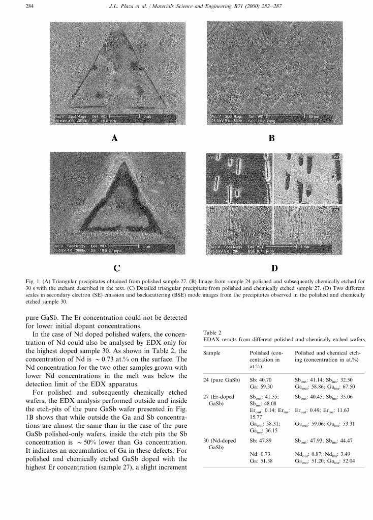
indications of surface damage in almost all the samples.Only the sample 27 with the highest Er concentrationhas shown clearly triangular precipitates of �10 mm insize after the polishing process. One of these precipi-tates is shown in detail in Fig. 1A. The formation ofthese precipitates with high Sb and Er concentrations,as demonstrated below by EDX analysis, could beexplained taking into account the tendency of REelements to form compounds with V group elementsknown as pnictides [10]. The existence of precipitateshas not been observed in Nd polished wafers even athigh dopant concentration. The same kind of analysishas been carried out for polished and subsequentlychemically etched wafers. Fig. 1B shows a SEM imagefrom the surface of the pure GaSb sample (sample 24).Triangular etch pits with a density of �106 cm−2 canbe observed. No main differences in the surface appear-ance between this wafer and the samples 25, 26, 28 and29 have been observed. Fig. 1C shows the surface of thesample 27 after polishing and chemical etching pro-cesses. In this case the precipitates shown in Fig. 1A forthe polished wafers appear also. It can be observed theeffect of the chemical etching which is more efficient atthe boundaries. Finally, Fig. 1D shows some precipi-tates present in the sample 30 (highest Nd concentra-tion) which could not be observed in polished wafers.This figure presents both images of secondary electronand backscattering images for two different scales.
The chemical composition of the polished wafers hasbeen analysed for different wafers and is shown inTable 2 for pure and the highest dopant concentration.It is observed that in the pure GaSb wafer (sample 24)the content of Sb is �30% lower than Ga. Thisdeviation from the stoichiometric composition couldexplain the anomalous high acceptor concentration (�1017 cm−3) in as-grown GaSb which has been tradition-ally attributed to Sb vacants and Ga antisites [11]. Thetriangular precipitates shown in Fig. 1A have also beenanalysed outside and inside indicated with ‘out’ and‘ins’ subscripts, respectively, in Table 2. These sub-scripts will be used along the text. It is observed that Erconcentration in these precipitates is about two ordersof magnitude higher inside than outside. The Sb con-centration is �15% higher inside than outside whileGa concentration is �40% lower in the former region.The Er content outside the precipitates are very lowand Ga and Sb concentrations are similar to that of the
Table 1Initial dopant concentration (×1019 cm−3) for the different GaSb grown ingots
Ingot 30 GaSb:NdIngot 24 pure Ingot 28 GaSb:Nd Ingot 29 GaSb:NdIngot 25 GaSb:Er Ingot 26 GaSb:Er Ingot 27 GaSb:ErGaSb
– 1.0 2.40.68 9.62.0
J.L. Plaza et al. / Materials Science and Engineering B71 (2000) 282–287284
Fig. 1. (A) Triangular precipitates obtained from polished sample 27. (B) Image from sample 24 polished and subsequently chemically etched for30 s with the etchant described in the text. (C) Detailed triangular precipitate from polished and chemically etched sample 27. (D) Two differentscales in secondary electron (SE) emission and backscattering (BSE) mode images from the precipitates observed in the polished and chemicallyetched sample 30.
pure GaSb. The Er concentration could not be detectedfor lower initial dopant concentrations.
In the case of Nd doped polished wafers, the concen-tration of Nd could also be analysed by EDX only forthe highest doped sample 30. As shown in Table 2, theconcentration of Nd is �0.73 at.% on the surface. TheNd concentration for the two other samples grown withlower Nd concentrations in the melt was below thedetection limit of the EDX apparatus.
For polished and subsequently chemically etchedwafers, the EDX analysis performed outside and insidethe etch-pits of the pure GaSb wafer presented in Fig.1B shows that while outside the Ga and Sb concentra-tions are almost the same than in the case of the pureGaSb polished-only wafers, inside the etch pits the Sbconcentration is �50% lower than Ga concentration.It indicates an accumulation of Ga in these defects. Forpolished and chemically etched GaSb doped with thehighest Er concentration (sample 27), a slight increment
Table 2EDAX results from different polished and chemically etched wafers
Sample Polished (con- Polished and chemical etch-ing (concentration in at.%)centration in
at.%)
Sbout: 41.14; Sbins: 32.50Sb: 40.7024 (pure GaSb)Ga: 59.30 Gaout: 58.86; Gains: 67.50
Sbout: 40.45; Sbins: 35.06Sbout: 41.55;27 (Er-dopedGaSb) Sbins: 48.08
Erout: 0.14; Erins: Erout: 0.49; Erins: 11.6315.77Gaout: 58.31; Gaout: 59.06; Gains: 53.31Gains: 36.15
30 (Nd-doped Sb: 47.89 Sbout: 47.93; Sbins: 44.47GaSb)
Nd: 0.73 Ndout: 0.87; Ndins: 3.49Ga: 51.38 Gaout: 51.20; Gains: 52.04
J.L. Plaza et al. / Materials Science and Engineering B71 (2000) 282–287 285
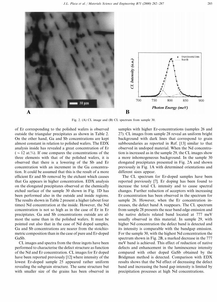
Fig. 2. (A) CL image and (B) CL spectrum from sample 30.
of Er corresponding to the polished wafers is observedoutside the triangular precipitates as shown in Table 2.On the other hand, Ga and Sb concentrations are keptalmost constant in relation to polished wafers. The EDXanalysis inside has revealed a great concentration of Er(�12 at.%). If one compares the concentrations of thethree elements with that of the polished wafers, it isobserved that there is a lowering of the Sb and Erconcentration with an increment in the Ga concentra-tion. It could be assumed that this is the result of a moreefficient Er and Sb removal by the etchant which causesthat Ga appears in higher concentration. EDX analysison the elongated precipitates observed at the chemicallyetched surface of the sample 30 shown in Fig. 1D hasbeen performed also in the outside and inside regions.The results shown in Table 2 present a higher (about fourtimes) Nd concentration at the inside. However, the Ndconcentration is not so high as in the case of Er in Erprecipitates. Ga and Sb concentrations outside are al-most the same than in the polished wafers. It must bepointed out also that in the case of Nd doped samples,Ga and Sb concentrations are nearer from the stoichio-metric composition than in the case of pure and Er-dopedGaSb.
CL images and spectra from the three ingots have beenperformed to characterise the defect structure as functionof the Nd and Er concentration. CL images for Er dopedhave been reported previously [12] where intensity of thelowest Er-doped sample 25 appeared rather uniformrevealing the subgrain structure. The same structure butwith smaller size of the grains has been observed in
samples with higher Er-concentrations (samples 26 and27). CL images from sample 28 reveal an uniform brightbackground with dark lines that correspond to grainsubboundaries as reported in Ref. [13] similar to thatobserved in undoped material. When the Nd concentra-tion is increased as in the sample 29, the CL images showa more inhomogeneous background. In the sample 30elongated precipitates presented in Fig. 2A and shownpreviously in Fig. 1A with determined orientations anddifferent sizes appear.
The CL spectrum for Er-doped samples have beenreported previously [7]. Er doping has been found toincrease the total CL intensity and to cause spectralchanges. Further reduction of acceptors with increasingEr concentration has been observed in the spectrum forsample 26. However, when the Er concentration in-creases, the defect band A reappears. The CL spectrumfrom sample 28 presents the near band edge emission andthe native defects related band located at 777 meVusually observed in this material. In sample 29, withhigher Nd concentration the defect band is detected andits intensity is comparable with the bandgap emission.For the sample 30, with the highest Nd concentration thespectrum shown in Fig. 2B, a marked decrease in the 777meV band is achieved. This effect of reduction of nativedefects and enhancement in the luminescence intensitycompared with other doped GaSb obtained by theBridgman method is detected. Comparison with EDXresults shows that the Nd effect of decreasing the defectband and increasing the band gap intensity is limited byprecipitation processes at high Nd concentrations.
J.L. Plaza et al. / Materials Science and Engineering B71 (2000) 282–287286
Table 3EDX results from different polished, chemically etched and thermallytreated wafers
Polished, chemically etched and thermallySampletreated wafers (concentration in at.%)
Sb: 39.0324 (pure GaSb)Ga: 60.97
27 (Er -doped Sbout: 41.93; Sbins: 26.97GaSb)
Erout: 0.36; Erins: 38.60Gaout: 57.71; Gains: 34.43
30 (Nd-doped Sbout: 45.91; Sbins: 31.47GaSb)
Ndout: 0.53; Ndins: 18.57Gaout: 53.56; Gains: 49.96
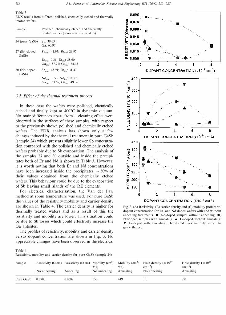
Fig. 3. (A) Resistivity, (B) carrier density and (C) mobility profiles vs.dopant concentration for Er- and Nd-doped wafers with and withoutannealing treatments. , Nd-doped samples without annealing. ,Nd-doped samples with annealing. �, Er-doped without annealing.�, Er-doped with annealing. The dotted lines are only shown toguide the eye.
3.2. Effect of the thermal treatment process
In these case the wafers were polished, chemicallyetched and finally kept at 400°C in dynamic vacuum.No main differences apart from a cleaning effect wereobserved in the surfaces of these samples, with respectto the previously shown polished and chemically etchedwafers. The EDX analysis has shown only a fewchanges induced by the thermal treatment in pure GaSb(sample 24) which presents slightly lower Sb concentra-tion compared with the polished and chemically etchedwafers probably due to Sb evaporation. The analysis ofthe samples 27 and 30 outside and inside the precipi-tates both of Er and Nd is shown in Table 3. However,it is worth noting that both Er and Nd concentrationshave been increased inside the precipitates �50% oftheir values obtained from the chemically etchedwafers. This behaviour could be due to the evaporationof Sb leaving small islands of the RE elements.
For electrical characterisation, the Van der Pawmethod at room temperature was used. For pure GaSbthe values of the resistivity mobility and carrier densityare shown in Table 4. The carrier density is higher forthermally treated wafers and as a result of this theresistivity and mobility are lower. This situation couldbe due to Sb losses which could effectively increase theGa antisites.
The profiles of resistivity, mobility and carrier densityversus dopant concentration are shown in Fig. 3. Noappreciable changes have been observed in the electrical
Table 4Resistivity, mobility and carrier density for pure GaSb (sample 24)
Hole density (×1017Mobility (cm2/Sample Mobility (cm2/Resistivity (V·cm) Hole density (×1017Resistivity (V·cm)cm−3) cm−3)V·s)V·s)
Annealing No annealing Annealing No annealing AnnealingNo annealing
2.01.04495500.06890.0900Pure GaSb
J.L. Plaza et al. / Materials Science and Engineering B71 (2000) 282–287 287
properties of polished and etched wafers so only theresults obtained for thermally and no-thermally treatedsamples are presented. It can be observed in Fig. 3Athat for low dopant concentration the resistivity de-crease with the increasing dopant concentration. Thisbehaviour is related to the increment in the carrierdensity which causes a diminishing mobility as shownin Fig. 3B and c, respectively. Only for the highestdoped samples the resistivity rises probably as a conse-quence of the precipitates which could act as recombi-nation centres.
As can be observed for similar dopant concentra-tions, the resistivity of the no-thermally treated Nd-doped wafers is slightly higher than for Er-dopedwafers in agreement with the higher carrier density inthe later case. The resistivity is decreased due to thethermal process in all the samples as shown in Fig. 3A.This behaviour is related to the increasing carrier den-sity as shown in Fig. 3B. This increment in the carrierdensity presented by the thermally treated samples is inagreement with the decreasing mobility shown in Fig.3C. This behaviour could be explained as a conse-quence of the evaporation of Sb atoms leaving siteswhich could be occupied by Ga and RE atoms. Both Erand Nd ions act with 3+ valence (rarely these ionspresent valence 2+ ), so the increment in the holeconcentration cannot be due to substitutional positionsof these ions replacing the Ga atoms because theisoelectronic nature of Ga, Er and Nd ions. In additiononly interstitial positions of the RE ions in the lattice orRESb antisites could explain these electronic behaviour.The position of RE in the lattice is still unclear andmore study is required on these features. It is worthnoting that the effect of the thermal treatment relatedto the increasing carrier density and, as a consequence,decreasing resistivity is more pronounced in the case ofthe samples doped with an intermediate level of dopant(samples 26 and 29). This observation is especiallynoted for Er-doped sample 29 where the resistivity isabout one order of magnitude higher in the case ofthermally tretated sample. For the highest Er (sample27) and Nd (sample 30) concentrations, the carrierdensity and mobility decrease probably due to precipi-tation resulting in a higher resistivity for these samples.As a consequence the thermal treatment has smalleffects in these samples.
4. Conclusions
In this work the formation of precipitates both of Erand Nd in GaSb grown by the vertical Bridgman methodfor an initial dopant concentration of 9×1019 cm−3 hasbeen demonstrated. These precipitates present a highconcentration of the RE element and Sb compared withthe surrounding material. The chemical etching alsoreveals a density of etch pits up to 106 cm−2 which showan excess of Ga at the inside. The reduction of the defectband induced by the RE elements has been demonstratedby CL. This effect is diminished for high dopantconcentrations due to precipitation phenomena.Electrical measurements showed that the thermaltreatments increase the carrier density. This effect is morepronounced for Er- and Nd-doped samples with adopant density of 2×1019 cm−3.
Acknowledgements
This work has been supported by CICYT under theproject ESP-98 1340.
References
[1] S. Coffa, A. Polman, R.N. Schwartz, Rare Earth Doped Semicon-ductors II, MRS Symposium Proceedings 422, Materials ResearchSociety, Pittsburg, 1996.
[2] A.R. Zanatta, L.A.O. Nunes, Appl. Phys. Lett. 71 (25) (1997) 3679.[3] L.F. Zakharenkov, V.A. Kasatkin, F.P. Kesamanly, B.E.
Samorukov, M.A. Sokolova, Sov. Phys. Semicond. 15 (1981) 946.[4] V.A. Kasatkin, F.P. Kesamanly, V.G. Makarenkov, V.F. Mas-
terov, B.E. Samorukov, Sov. Phys. Semicond. 14 (1980) 1092.[5] V.A. Kasatkin, F.P. Kesamanly, B.E. Samorukov, Sov. Phys.
Semicond. 15 (1981) 352.[6] H. Ennen, J. Schneider, J. Electron. Mater. 14A (1985) 115.[7] P. Hidalgo, B. Mendez, J. Piqueras, J. Plaza, E. Dieguez, Semicond.
Sci. Technol. 13 (1998) 1431.[8] T.J. Zhang, S.Y. Li, Solid State Electron. 29 (1986) 775.[9] P.S. Dutta, K.S. Koteswara Rao, H.L. Bhat, K. Gopalakrihna
Naik, V. Kumar, J. Cryst. Growth 155 (1995) 3702.[10] M.E. Mullen, B. Luthi, P.S. Wang, E. Bucher, L.D. Longinotti,
J.P. Maita, Phys. Rev. B 10 (1974) 1.[11] M. Ichimura, K. Higuchi, Y. Hattori, T. Wada, N. Kitamura, J.
Appl. Phys. 68 (1990) 6153.[12] J.L. Plaza, P. Hidalgo, B. Mendez, J. Piqueras, J.L. Castano, E.
Dieguez, J. Cryst. Growth 198 (1999) 379.[13] B. Mendez, J. Piqueras, P.S. Dutta, E. Dieguez, Appl. Phys. Lett.
67 (1995) 2648.
.