Embed Size (px)
Citation preview

PolarFire FPGA Macro Library Guide

MicrosHeadqOne EntCA 9265
Within thOutsideSales: +Fax: +1 E-mail: s
ctortrialnal
andns;ies,ns;nia,
© 2017rights rMicroseMicrosetrademaproperty
n oranysold not areand relyer'sThentirey orucht is
this
emi Corporate uarterserprise, Aliso Viejo,6 USA
e USA: +1 (800) 713-4113 the USA: +1 (949) 380-61001 (949) 380-6136(949) [email protected]
Microsemi Corporation (Nasdaq: MSCC) offers a comprehensive portfolio of semiconduand system solutions for communications, defense and security, aerospace, and indusmarkets. Products include high-performance and radiation-hardened analog mixed-sigintegrated circuits, FPGAs, SoCs, and ASICs; power management products; timing synchronization devices and precise time solutions; voice processing devices; RF solutiodiscrete components; enterprise storage and communications solutions, security technologand scalable anti-tamper products; Ethernet solutions; Power-over-Ethernet ICs and midspacustom design capabilities and services. Microsemi is headquartered in Aliso Viejo, Califorand has approximately 4,800 employees worldwide. Learn more at www.microsemi.com.
Microsemi Corporation. Alleserved. Microsemi and themi logo are trademarks ofmi Corporation. All otherrks and service marks are the
Microsemi makes no warranty, representation, or guarantee regarding the information contained hereithe suitability of its products and services for any particular purpose, nor does Microsemi assume liability whatsoever arising out of the application or use of any product or circuit. The products hereunder and any other products sold by Microsemi have been subject to limited testing and shouldbe used in conjunction with mission-critical equipment or applications. Any performance specificationsbelieved to be reliable but are not verified, and Buyer must conduct and complete all performance other testing of the products, alone and together with, or installed in, any end-products. Buyer shall noton any data and performance specifications or parameters provided by Microsemi. It is the Buyresponsibility to independently determine suitability of any products and to test and verify the same. information provided by Microsemi hereunder is provided “as is, where is” and with all faults, and the erisk associated with such information is entirely with the Buyer. Microsemi does not grant, explicitlimplicitly, to any party any patent rights, licenses, or any other IP rights, whether with regard to sinformation itself or anything described by such information. Information provided in this documenproprietary to Microsemi, and Microsemi reserves the right to make any changes to the information in
50200718-4/10.17
of their respective owners. document or to any products and services at any time without notice.
3
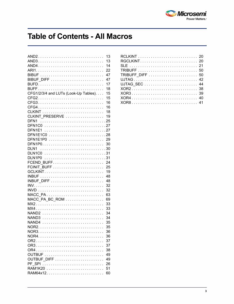
Table of Contents - All Macros
AND2 . . . . . . . . . . . . . . . . . . . . . . . . . . . . . . . 13AND3 . . . . . . . . . . . . . . . . . . . . . . . . . . . . . . . 13AND4 . . . . . . . . . . . . . . . . . . . . . . . . . . . . . . . 14ARI1. . . . . . . . . . . . . . . . . . . . . . . . . . . . . . . . 22BIBUF . . . . . . . . . . . . . . . . . . . . . . . . . . . . . . 47BIBUF_DIFF . . . . . . . . . . . . . . . . . . . . . . . . . 47BUFD. . . . . . . . . . . . . . . . . . . . . . . . . . . . . . . 17BUFF . . . . . . . . . . . . . . . . . . . . . . . . . . . . . . . 18CFG1/2/3/4 and LUTs (Look-Up Tables). . . . 15CFG2 . . . . . . . . . . . . . . . . . . . . . . . . . . . . . . . 15CFG3 . . . . . . . . . . . . . . . . . . . . . . . . . . . . . . . 16CFG4 . . . . . . . . . . . . . . . . . . . . . . . . . . . . . . . 16CLKINT . . . . . . . . . . . . . . . . . . . . . . . . . . . . . 18CLKINT_PRESERVE . . . . . . . . . . . . . . . . . . 19DFN1 . . . . . . . . . . . . . . . . . . . . . . . . . . . . . . . 25DFN1C0 . . . . . . . . . . . . . . . . . . . . . . . . . . . . . 27DFN1E1 . . . . . . . . . . . . . . . . . . . . . . . . . . . . . 27DFN1E1C0 . . . . . . . . . . . . . . . . . . . . . . . . . . . 28DFN1E1P0 . . . . . . . . . . . . . . . . . . . . . . . . . . 29DFN1P0. . . . . . . . . . . . . . . . . . . . . . . . . . . . . 30DLN1 . . . . . . . . . . . . . . . . . . . . . . . . . . . . . . . 30DLN1C0 . . . . . . . . . . . . . . . . . . . . . . . . . . . . . 31DLN1P0 . . . . . . . . . . . . . . . . . . . . . . . . . . . . . 31FCEND_BUFF. . . . . . . . . . . . . . . . . . . . . . . . 24FCINIT_BUFF . . . . . . . . . . . . . . . . . . . . . . . . 25GCLKINT . . . . . . . . . . . . . . . . . . . . . . . . . . . . 19INBUF . . . . . . . . . . . . . . . . . . . . . . . . . . . . . . 48INBUF_DIFF . . . . . . . . . . . . . . . . . . . . . . . . . 48INV. . . . . . . . . . . . . . . . . . . . . . . . . . . . . . . . . 32INVD . . . . . . . . . . . . . . . . . . . . . . . . . . . . . . . 32MACC_PA . . . . . . . . . . . . . . . . . . . . . . . . . . . 63MACC_PA_BC_ROM . . . . . . . . . . . . . . . . . . 69MX2 . . . . . . . . . . . . . . . . . . . . . . . . . . . . . . . . 33MX4 . . . . . . . . . . . . . . . . . . . . . . . . . . . . . . . . 33NAND2 . . . . . . . . . . . . . . . . . . . . . . . . . . . . . 34NAND3 . . . . . . . . . . . . . . . . . . . . . . . . . . . . . 34NAND4 . . . . . . . . . . . . . . . . . . . . . . . . . . . . . 35NOR2. . . . . . . . . . . . . . . . . . . . . . . . . . . . . . . 35NOR3. . . . . . . . . . . . . . . . . . . . . . . . . . . . . . . 36NOR4. . . . . . . . . . . . . . . . . . . . . . . . . . . . . . . 36OR2 . . . . . . . . . . . . . . . . . . . . . . . . . . . . . . . . 37OR3 . . . . . . . . . . . . . . . . . . . . . . . . . . . . . . . . 37OR4 . . . . . . . . . . . . . . . . . . . . . . . . . . . . . . . . 38OUTBUF . . . . . . . . . . . . . . . . . . . . . . . . . . . . 49OUTBUF_DIFF . . . . . . . . . . . . . . . . . . . . . . . 49PF_SPI . . . . . . . . . . . . . . . . . . . . . . . . . . . . . 26RAM1K20 . . . . . . . . . . . . . . . . . . . . . . . . . . . 51RAM64x12. . . . . . . . . . . . . . . . . . . . . . . . . . . 60
RCLKINT . . . . . . . . . . . . . . . . . . . . . . . . . . . . 20RGCLKINT. . . . . . . . . . . . . . . . . . . . . . . . . . . 20SLE . . . . . . . . . . . . . . . . . . . . . . . . . . . . . . . . 21TRIBUFF . . . . . . . . . . . . . . . . . . . . . . . . . . . . 50TRIBUFF_DIFF . . . . . . . . . . . . . . . . . . . . . . . 50UJTAG . . . . . . . . . . . . . . . . . . . . . . . . . . . . . . 42UJTAG_SEC . . . . . . . . . . . . . . . . . . . . . . . . . 44XOR2 . . . . . . . . . . . . . . . . . . . . . . . . . . . . . . . 38XOR3 . . . . . . . . . . . . . . . . . . . . . . . . . . . . . . . 39XOR4 . . . . . . . . . . . . . . . . . . . . . . . . . . . . . . . 40XOR8 . . . . . . . . . . . . . . . . . . . . . . . . . . . . . . . 41

4
Table of Contents - Combinatorial Logic
AND2 . . . . . . . . . . . . . . . . . . . . . . . . . . . . . . . 13AND3 . . . . . . . . . . . . . . . . . . . . . . . . . . . . . . . 13AND4 . . . . . . . . . . . . . . . . . . . . . . . . . . . . . . . 14ARI1. . . . . . . . . . . . . . . . . . . . . . . . . . . . . . . . 22BUFD. . . . . . . . . . . . . . . . . . . . . . . . . . . . . . . 17BUFF . . . . . . . . . . . . . . . . . . . . . . . . . . . . . . . 18CFG1/2/3/4 and LUTs (Look-Up Tables). . . . 15CFG2 . . . . . . . . . . . . . . . . . . . . . . . . . . . . . . . 15CFG3 . . . . . . . . . . . . . . . . . . . . . . . . . . . . . . . 16CFG4 . . . . . . . . . . . . . . . . . . . . . . . . . . . . . . . 16INV. . . . . . . . . . . . . . . . . . . . . . . . . . . . . . . . . 32INVD . . . . . . . . . . . . . . . . . . . . . . . . . . . . . . . 32MX2 . . . . . . . . . . . . . . . . . . . . . . . . . . . . . . . . 33MX4 . . . . . . . . . . . . . . . . . . . . . . . . . . . . . . . . 33NAND2 . . . . . . . . . . . . . . . . . . . . . . . . . . . . . 34NAND3 . . . . . . . . . . . . . . . . . . . . . . . . . . . . . 34NAND4 . . . . . . . . . . . . . . . . . . . . . . . . . . . . . 35NOR2. . . . . . . . . . . . . . . . . . . . . . . . . . . . . . . 35NOR3. . . . . . . . . . . . . . . . . . . . . . . . . . . . . . . 36NOR4. . . . . . . . . . . . . . . . . . . . . . . . . . . . . . . 36OR2 . . . . . . . . . . . . . . . . . . . . . . . . . . . . . . . . 37OR3 . . . . . . . . . . . . . . . . . . . . . . . . . . . . . . . . 37OR4 . . . . . . . . . . . . . . . . . . . . . . . . . . . . . . . . 38XOR2. . . . . . . . . . . . . . . . . . . . . . . . . . . . . . . 38XOR3. . . . . . . . . . . . . . . . . . . . . . . . . . . . . . . 39XOR4. . . . . . . . . . . . . . . . . . . . . . . . . . . . . . . 40XOR8. . . . . . . . . . . . . . . . . . . . . . . . . . . . . . . 41

5
Table of Contents - Sequential Logic
DFN1 . . . . . . . . . . . . . . . . . . . . . . . . . . . . . . . 25DFN1C0 . . . . . . . . . . . . . . . . . . . . . . . . . . . . . 27DFN1E1 . . . . . . . . . . . . . . . . . . . . . . . . . . . . . 27DFN1E1C0 . . . . . . . . . . . . . . . . . . . . . . . . . . . 28DFN1E1P0 . . . . . . . . . . . . . . . . . . . . . . . . . . 29DFN1P0. . . . . . . . . . . . . . . . . . . . . . . . . . . . . 30DLN1 . . . . . . . . . . . . . . . . . . . . . . . . . . . . . . . 30DLN1C0 . . . . . . . . . . . . . . . . . . . . . . . . . . . . . 31DLN1P0 . . . . . . . . . . . . . . . . . . . . . . . . . . . . . 31SLE . . . . . . . . . . . . . . . . . . . . . . . . . . . . . . . . 21

6
Table of Contents - RAM Blocks
RAM1K20 . . . . . . . . . . . . . . . . . . . . . . . . . . . 51RAM64x12. . . . . . . . . . . . . . . . . . . . . . . . . . . 60

7
Table of Contents - Math Blocks
MACC_PA . . . . . . . . . . . . . . . . . . . . . . . . . . . 63MACC_PA_BC_ROM . . . . . . . . . . . . . . . . . . 69

8
Table of Contents - I/Os
BIBUF . . . . . . . . . . . . . . . . . . . . . . . . . . . . . . 47BIBUF_DIFF . . . . . . . . . . . . . . . . . . . . . . . . . 47INBUF . . . . . . . . . . . . . . . . . . . . . . . . . . . . . . 48INBUF_DIFF . . . . . . . . . . . . . . . . . . . . . . . . . 48OUTBUF . . . . . . . . . . . . . . . . . . . . . . . . . . . . 49OUTBUF_DIFF . . . . . . . . . . . . . . . . . . . . . . . 49TRIBUFF . . . . . . . . . . . . . . . . . . . . . . . . . . . . 50TRIBUFF_DIFF . . . . . . . . . . . . . . . . . . . . . . . 50UJTAG. . . . . . . . . . . . . . . . . . . . . . . . . . . . . . 42UJTAG_SEC . . . . . . . . . . . . . . . . . . . . . . . . . 44

9
Table of Contents - Clocking
CLKINT . . . . . . . . . . . . . . . . . . . . . . . . . . . . . 18CLKINT_PRESERVE . . . . . . . . . . . . . . . . . . 19GCLKINT . . . . . . . . . . . . . . . . . . . . . . . . . . . . 19RCLKINT . . . . . . . . . . . . . . . . . . . . . . . . . . . . 20RGCLKINT . . . . . . . . . . . . . . . . . . . . . . . . . . 20

10
Table of Contents - Special
FCEND_BUFF. . . . . . . . . . . . . . . . . . . . . . . . 24FCINIT_BUFF . . . . . . . . . . . . . . . . . . . . . . . . 25PF_SPI . . . . . . . . . . . . . . . . . . . . . . . . . . . . . 26
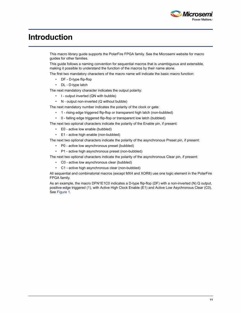
Introduction
This macro library guide supports the PolarFire FPGA family. See the Microsemi website for macro guides for other families.
This guide follows a naming convention for sequential macros that is unambiguous and extensible, making it possible to understand the function of the macros by their name alone.
The first two mandatory characters of the macro name will indicate the basic macro function:
• DF - D-type flip-flop
• DL - D-type latch
The next mandatory character indicates the output polarity:
• I - output inverted (QN with bubble)
• N - output non-inverted (Q without bubble)
The next mandatory number indicates the polarity of the clock or gate:
• 1 - rising edge triggered flip-flop or transparent high latch (non-bubbled)
• 0 - falling edge triggered flip-flop or transparent low latch (bubbled)
The next two optional characters indicate the polarity of the Enable pin, if present:
• E0 - active low enable (bubbled)
• E1 - active high enable (non-bubbled)
The next two optional characters indicate the polarity of the asynchronous Preset pin, if present:
• P0 - active low asynchronous preset (bubbled)
• P1 - active high asynchronous preset (non-bubbled)
The next two optional characters indicate the polarity of the asynchronous Clear pin, if present:
• C0 - active low asynchronous clear (bubbled)
• C1 - active high asynchronous clear (non-bubbled)
All sequential and combinatorial macros (except MX4 and XOR8) use one logic element in the PolarFire FPGA family.
As an example, the macro DFN1E1C0 indicates a D-type flip-flop (DF) with a non-inverted (N) Q output, positive-edge triggered (1), with Active High Clock Enable (E1) and Active Low Asychronous Clear (C0). See Figure 1.
11

Figure 1 • Naming Convention
Truth Table NotationThe truth table states in this User Guide are defined as follows:
State Meaning
0 Logic “0”
1 Logic “1”
X Don't Care (for Inputs), Unknown (for Outputs)
Z High Impedance
12
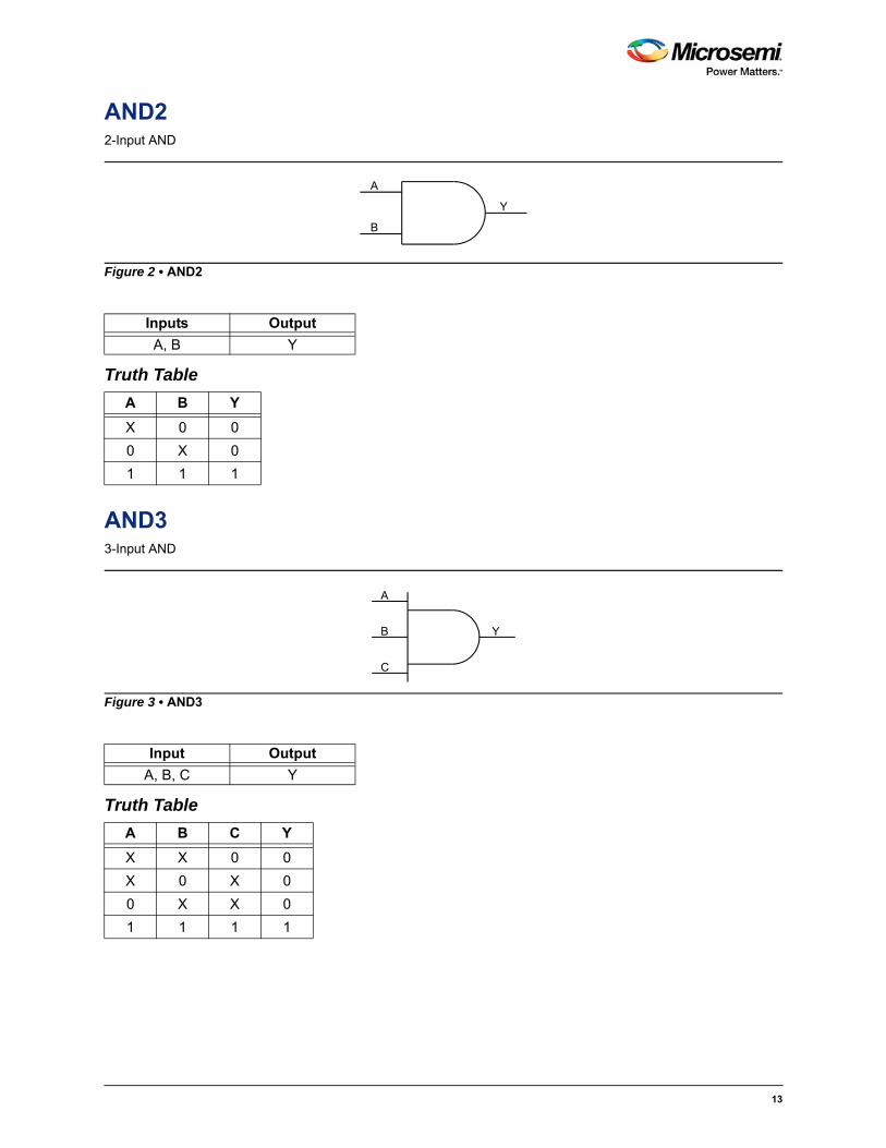
AND22-Input AND
Truth Table
AND33-Input AND
Truth Table
Figure 2 • AND2
Inputs Output
A, B Y
A B Y
X 0 0
0 X 0
1 1 1
Figure 3 • AND3
Input Output
A, B, C Y
A B C Y
X X 0 0
X 0 X 0
0 X X 0
1 1 1 1
A
B
Y
Y
C
B
A
13

PolarFire Macro Library Guide
AND44-Input AND
Truth Table
Figure 4 • AND4
Input Output
A, B, C, D Y
A B C D Y
X X X 0 0
X X 0 X 0
X 0 X X 0
0 X X X 0
1 1 1 1 1
Y
C
B
A
D
14

CFG1/2/3/4 and LUTs (Look-Up Tables)CFG1, CFG2, CFG3, and CFG4 are post-layout LUTs (Look-up table) used to implement any 1-input, 2-input, 3-input, and 4-input combinational logic functions, respectively. Each of the CFG1/2/3/4 macros has an INIT string parameter that determines the logic functions of the macro. The output Y is dependent on the INIT string parameter and the values of the inputs.
CFG2Post-layout macro used to implement any 2-input combinational logic function. Output Y is dependent on the INIT string parameter and the value of A and B. The INIT string parameter is 4 bits wide.
Table 1 • CFG2 INIT String InterpretationI
Figure 5 • CFG2
Input Output
A,B Y = f (INIT, A, B)
BA Y
00 INIT[0]
01 INIT[1]
10 INIT[2]
11 INIT[3]
15

PolarFire Macro Library Guide
CFG3Post-layout macro used to implement any 3-input combinational logic function. Output Y is dependent on the INIT string parameter and the value of A,B, and C. The INIT string parameter is 8 bits wide.
.
Table 2 • CFG3 INIT String Interpretation
CFG4Post-layout macro used to implement any 4-input combinational logic function. Output Y is dependent on the INIT string parameter and the value of A,B, C, and D. The INIT string parameter is 16 bits wide.
Figure 6 • CFG3
Input Output
A, B, C Y = f (INIT, A,B, C)
CBA Y
000 INIT[0]
001 INIT[1]
010 INIT[2]
011 INIT[3]
100 INIT[4]
101 INIT[5]
110 INIT[6]
111 INIT[7]
Figure 7 • CFG4
16

Table 3 • CFG4 INIT String Interpretation
BUFDBuffer. Note that Compile optimization will not remove this macro.
Truth Table
Input Output
A, B, C, D Y = f (INIT, A,B, C, D)
DCBA Y
0000 INIT[0]
0001 INIT[1]
0010 INIT[2]
0011 INIT[3]
0100 INIT[4]
0101 INIT[5]
0110 INIT[6]
0111 INIT[7]
1000 INIT[8]
1001 INIT[9]
1010 INIT[10]
1011 INIT[11]
1100 INIT[12]
1101 INIT[13]
1110 INIT[14]
1111 INIT[15]
Figure 8 • BUFD
Input Output
A Y
A Y
0 0
1 1
A Y
17

PolarFire Macro Library Guide
BUFFBuffer
Truth Table
CLKINTMacro used to route an internal fabric signal to global network.
Truth Table
Figure 9 • BUFF
Input Output
A Y
A Y
0 0
1 1
Figure 10 • CLKINT
Input Output
A Y
A Y
0 0
1 1
A Y
A Y
18

CLKINT_PRESERVEMacro used to route an internal fabric signal to global network. It has the same functionality as CLKINT except that this clock always stay on the global clock network and will not be demoted during design implementation.
Truth Table
GCLKINTGated macro used to route an internal fabric signal to global network. The Enable signal can be used to turn off the global network to save power.
Truth Table
Figure 11 • CLKINT_PRESERVE
Input Output
A Y
A Y
0 0
1 1
Figure 12 • GCLKINT
Input Output
A, EN Y
A ENq
(Internal Signal)
Output
0 0 0 0
0 1 1 0
1 X q q
A Y
19
PolarFire Macro Library Guide
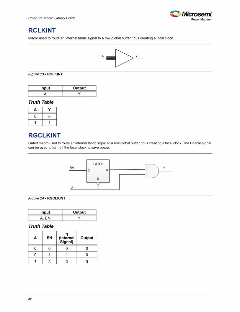
RCLKINTMacro used to route an internal fabric signal to a row global buffer, thus creating a local clock.
Truth Table
RGCLKINTGated macro used to route an internal fabric signal to a row global buffer, thus creating a local clock. The Enable signal can be used to turn off the local clock to save power.
Truth Table
Figure 13 • RCLKINT
Input Output
A Y
A Y
0 0
1 1
Figure 14 • RGCLKINT
Input Output
A, EN Y
A ENq
(Internal Signal)
Output
0 0 0 0
0 1 1 0
1 X q q
A Y
20

SLESequential Logic Element
*Note: ADn, SD and LAT are static signals defined at design time and need to be tied to 0 or 1.
Truth Table
Figure 15 • SLE
Input Output
Name Function
Q
D Data
CLK Clock
EN Enable
ALn Asynchronous Load (Active Low)
ADn* Asynchronous Data (Active Low)
SLn Synchronous Load (Active Low)
SD* Synchronous Data
LAT* Latch Enable
ALn ADn LAT CLK EN SLn SD D Qn+1
0 ADn X X X X X X !ADn
1 X 0 Not rising X X X X Qn
1 X 0 0 X X X Qn
1 X 0 1 0 SD X SD
1 X 0 1 1 X D D
1 X 1 0 X X X X Qn
1 X 1 1 0 X X X Qn
1 X 1 1 1 0 SD X SD
1 X 1 1 1 1 X D D
DCLK
ENALnADn
SLn
SD
LAT
Q
21

PolarFire Macro Library Guide
ARI1The ARI1 macro is responsible for representing all arithmetic operations in the pre-layout phase.
The ARI1 cell has a 20bit INIT string parameter that is used to configure its functionality. The interpretation of the 16 LSB of the INIT string is shown in the table below. F0 is the value of Y when A = 0 and F1 is the value of Y when A = 1.
Figure 16 • ARI1
Input Output
A, B, C, D, FCI Y, S, FCO
Table 4 • Interpretation of 16 LSB of the INIT String for ARI1
ADCB Y
0000 INIT[0] F0
0001 INIT[1]
0010 INIT[2]
0011 INIT[3]
0100 INIT[4]
0101 INIT[5]
0110 INIT[6]
0111 INIT[7]
1000 INIT[8] F1
1001 INIT[9]
1010 INIT[10]
1011 INIT[11]
1100 INIT[12]
1101 INIT[13]
1110 INIT[14]
1111 INIT[15]
AB
C
D
FCI
Y
S
FCO
22

The 4 MSB of the INIT string controls the output of the carry bits. The carry is generated using carry propagation and generation bits, which are evaluated according to the tables below.
Table 5 • Truth Table for S
Y FCI S
0 0 0
0 1 1
1 0 1
1 1 0
Figure 17 • ARI1 Logic
Table 6 • ARI1 INIT[17:16] String Interpretation
INIT[17] INIT[16] G
0 0 0
0 1 F0
1 0 1
1 1 F1
23

PolarFire Macro Library Guide
FCEND_BUFFBuffer, driven by the FCO pin of the last macro in the Carry-Chain.
Truth Table
Table 7 • ARI1 INIT[19:18] String Interpretation
INIT[19] INIT[18] P
0 0 0
0 1 Y
1 X 1
Table 8 • FCO Truth Table
P G FCI FCO
0 G X G
1 X FCI FCI
Figure 18 • FCEND_BUFF
Input Output
A Y
A Y
0 0
1 1
A Y
24

FCINIT_BUFFBuffer, used to initialize the FCI pin of the first macro in the Carry-Chain.
Truth Table
DFN1D-Type Flip-Flop
Truth Table
Figure 19 • FCINIT_BUFF
Input Output
A Y
A Y
0 0
1 1
Figure 20 • DFN1
Input Output
D, CLK Q
CLK D Qn+1
not Rising X Qn
D D
A Y
Q
CLK
D
25
PolarFire Macro Library Guide
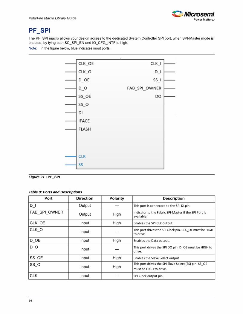
PF_SPIThe PF_SPI macro allows your design access to the dedicated System Controller SPI port, when SPI-Master mode is enabled, by tying both SC_SPI_EN and IO_CFG_INTF to high.
Note: In the figure below, blue indicates inout ports.
Figure 21 • PF_SPI
Table 9: Ports and Descriptions
Port Direction Polarity Description
D_I Output — This port is connected to the SPI DI pin
FAB_SPI_OWNER Output High Indicator to the Fabric SPI‐Master if the SPI Port is available.
CLK_OE Input High Enables the SPI CLK output.
CLK_O Input — This port drives the SPI Clock pin. CLK_OE must be HIGH to drive.
D_OE Input High Enables the Data output.
D_O Input — This port drives the SPI DO pin. D_OE must be HIGH to drive.
SS_OE Input High Enables the Slave Select output
SS_O Input HighThis port drives the SPI Slave Select (SS) pin. SS_OE
must be HIGH to drive.
CLK Inout — SPI Clock output pin.
26

DFN1C0D-Type Flip-Flop with active low Clear
Truth Table
DFN1E1D-Type Flip-Flop with active high Enable
DI Input — SPI Serial Data input pin.
DO Output — SPI Serial Data output pin.
SS Inout High SPI Slave Select output pin
IFACEInput High
This port is mapped to the IO_CFG_INTF pin. This pin must be tied to high together with the SC_SPI_EN pin to enable SPI port for the fabric macro to work.
FLASHInput High
This port is mapped to the SC_SPI_EN pin. This pin must be tied to high together with the IO_CFG_INTF pin to enable the SPI port for fabric macro to work.
Figure 22 • DFN1C0
Input Output
D, CLK, CLR Q
CLR CLK D Qn+1
0 X X 0
1 not Rising X Qn
1 D D
Figure 23 • DFN1E1
Table 9: Ports and Descriptions (Continued)
Port Direction Polarity Description
Q
CLR
CLK
D
Q
CLK
E
D
27

PolarFire Macro Library Guide
Truth Table
DFN1E1C0D-Type Flip-Flop, with active high Enable and active low Clear.
Truth Table
Input Output
D, E, CLK Q
E CLK D Qn+1
0 X X Qn
1 not Rising X Qn
1 D D
Figure 24 • DFN1E1C0
Input Output
CLR, D, E, CLK Q
CLR E CLK D Qn+1
0 X X X 0
1 0 X X Qn
1 1 not Rising X Qn
1 1 D D
Q
CLRCLK
E
D
28

DFN1E1P0D-Type Flip-Flop with active high Enable and active low Preset.
Truth Table
Figure 25 • DFN1E1P0
Input Output
D, E, PRE, CLK Q
PRE E CLK D Qn+1
0 X X X 1
1 0 X X Qn
1 1 not Rising X Qn
1 1 D D
QPRE
CLK
E
D
29

PolarFire Macro Library Guide
DFN1P0D-Type Flip-Flop with active low Preset.
Truth Table
DLN1Data Latch
Truth Table
Figure 26 • DFN1P0
Input Output
D, PRE, CLK Q
PRE CLK D Qn+1
0 X X 1
1 not Rising X Qn
1 D D
Figure 27 • DLN1
Input Output
D, G Q
G D Q
0 X Q
1 D D
Q
PRE
CLK
D
Q
G
D
30

DLN1C0Data Latch with active low Clear
Truth Table
DLN1P0Data Latch with active low Preset
Truth Table
Figure 28 • DLN1C0
Input Output
CLR, D, G Q
CLR G D Q
0 X X 0
1 0 X Q
1 1 D D
Figure 29 • DLN1P0
Input Output
D, G, PRE Q
PRE G D Q
0 X X 1
1 0 X Q
1 1 D D
Q
CLRG
D
D
G
PRE Q
31
PolarFire Macro Library Guide
INVInverter
Truth Table
INVDInverter; note that Compile optimization will not remove this macro.
Truth Table
Figure 30 • INV
Input Output
A Y
A Y
0 1
1 0
Figure 31 • INVD
Input Output
A Y
A Y
0 1
1 0
YA
YA
32
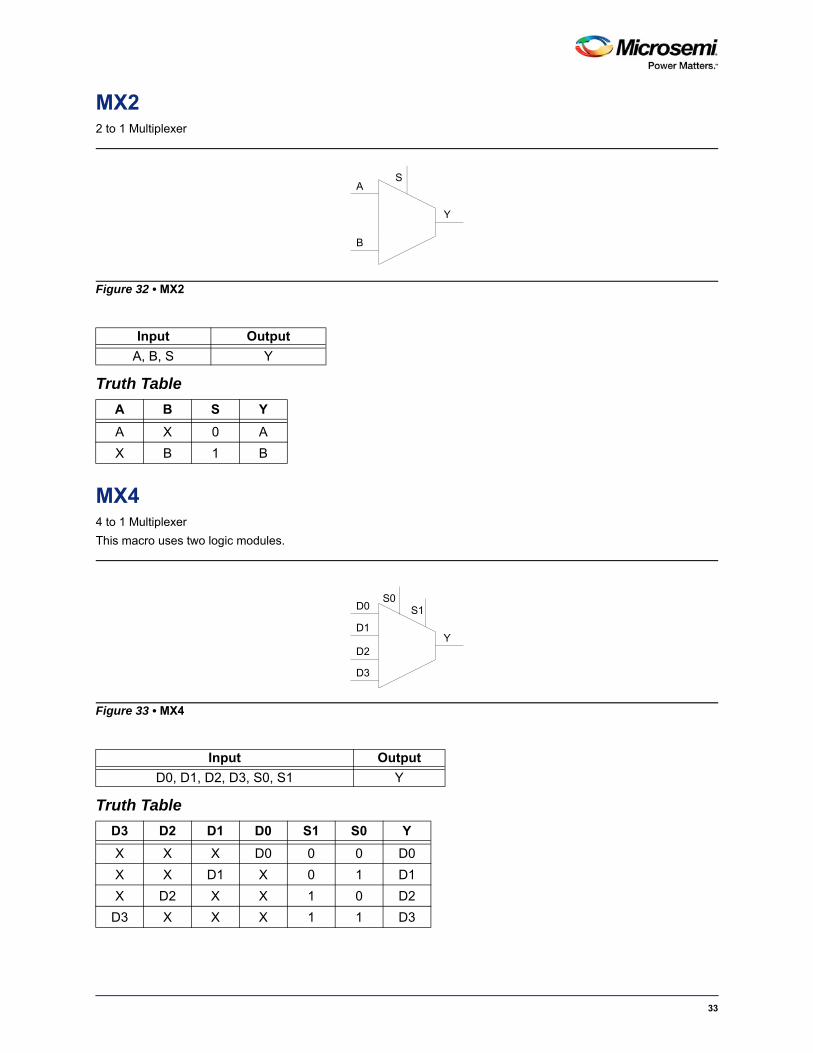
MX22 to 1 Multiplexer
Truth Table
MX44 to 1 Multiplexer
This macro uses two logic modules.
Truth Table
Figure 32 • MX2
Input Output
A, B, S Y
A B S Y
A X 0 A
X B 1 B
Figure 33 • MX4
Input Output
D0, D1, D2, D3, S0, S1 Y
D3 D2 D1 D0 S1 S0 Y
X X X D0 0 0 D0
X X D1 X 0 1 D1
X D2 X X 1 0 D2
D3 X X X 1 1 D3
S
Y
B
A
S0
Y
D3
D0
D1
D2
S1
33

PolarFire Macro Library Guide
NAND22-Input NAND
Truth Table
NAND33-Input NAND
Truth Table
Figure 34 • NAND2
Input Output
A, B Y
A B Y
X 0 1
0 X 1
1 1 0
Figure 35 • NAND3
Input Output
A, B, C Y
A B C Y
X X 0 1
X 0 X 1
0 X X 1
1 1 1 0
B
YA
B
C
Y
A
34
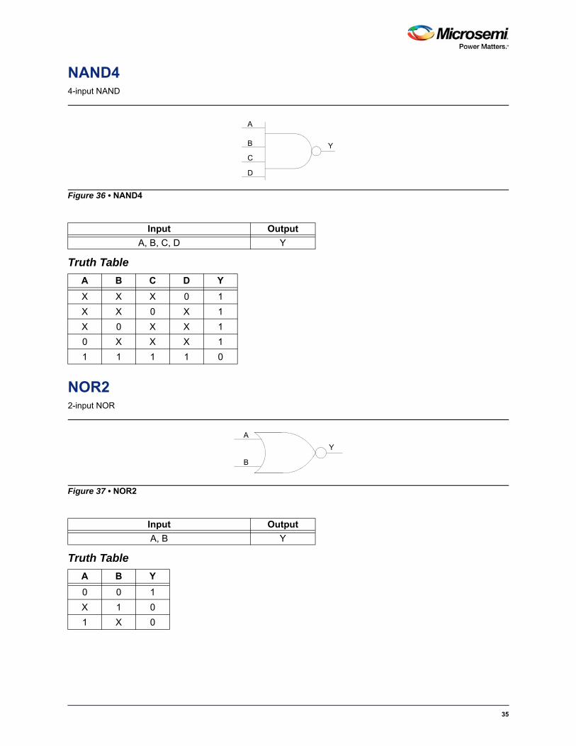
NAND44-input NAND
Truth Table
NOR22-input NOR
Truth Table
Figure 36 • NAND4
Input Output
A, B, C, D Y
A B C D Y
X X X 0 1
X X 0 X 1
X 0 X X 1
0 X X X 1
1 1 1 1 0
Figure 37 • NOR2
Input Output
A, B Y
A B Y
0 0 1
X 1 0
1 X 0
B
C
Y
A
D
A
B
Y
35

PolarFire Macro Library Guide
NOR33-input NOR
Truth Table
NOR44-input NOR
Truth Table
Figure 38 • NOR3
Input Output
A, B, C Y
A B C Y
0 0 0 1
X X 1 0
X 1 X 0
1 X X 0
Figure 39 • NOR4
Input Output
A, B, C, D Y
A B C D Y
0 0 0 0 1
1 X X X 0
X 1 X X 0
X X 1 X 0
X X X 1 0
Y
C
B
A
Y
D
B
A
C
36

OR22-input OR
Truth Table
OR33-input OR
Truth Table
Figure 40 • OR2
Input Output
A, B Y
A B Y
0 0 0
X 1 1
1 X 1
Figure 41 • OR3
Input Output
A, B, C Y
A B C Y
0 0 0 0
X X 1 1
X 1 X 1
1 X X 1
A
Y
B
Y
C
B
A
37
PolarFire Macro Library Guide
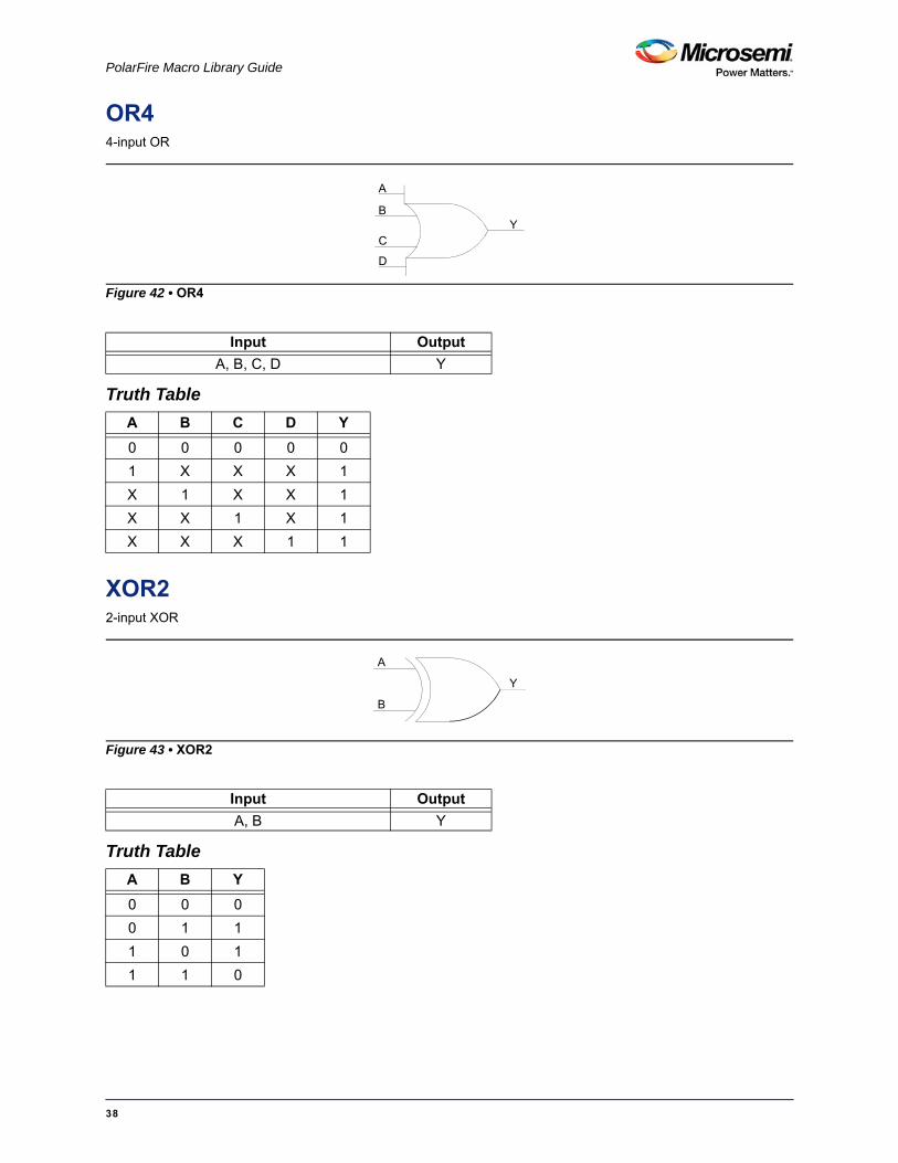
OR44-input OR
Truth Table
XOR22-input XOR
Truth Table
Figure 42 • OR4
Input Output
A, B, C, D Y
A B C D Y
0 0 0 0 0
1 X X X 1
X 1 X X 1
X X 1 X 1
X X X 1 1
Figure 43 • XOR2
Input Output
A, B Y
A B Y
0 0 0
0 1 1
1 0 1
1 1 0
Y
D
B
A
C
Y
B
A
38

XOR33-input XOR
Truth Table
Figure 44 • XOR3
Input Output
A, B, C Y
A B C Y
0 0 0 0
1 0 0 1
0 1 0 1
1 1 0 0
0 0 1 1
1 0 1 0
0 1 1 0
1 1 1 1
Y
C
A
B
39
PolarFire Macro Library Guide
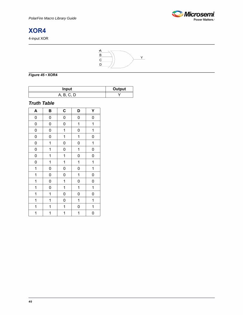
XOR44-input XOR
Truth Table
Figure 45 • XOR4
Input Output
A, B, C, D Y
A B C D Y
0 0 0 0 0
0 0 0 1 1
0 0 1 0 1
0 0 1 1 0
0 1 0 0 1
0 1 0 1 0
0 1 1 0 0
0 1 1 1 1
1 0 0 0 1
1 0 0 1 0
1 0 1 0 0
1 0 1 1 1
1 1 0 0 0
1 1 0 1 1
1 1 1 0 1
1 1 1 1 0
YC
AB
D
40
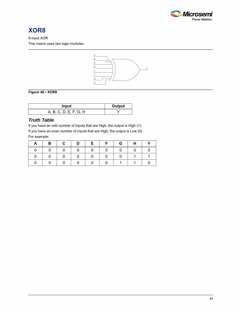
XOR88-input XOR
This macro uses two logic modules.
Truth Table If you have an odd number of inputs that are High, the output is High (1).
If you have an even number of inputs that are High, the output is Low (0).
For example:
Figure 46 • XOR8
Input Output
A, B, C, D, E, F, G, H Y
A B C D E F G H Y
0 0 0 0 0 0 0 0 0
0 0 0 0 0 0 0 1 1
0 0 0 0 0 0 1 1 0
A
Y
B
C
E
F
G
H
D
41
PolarFire Macro Library Guide
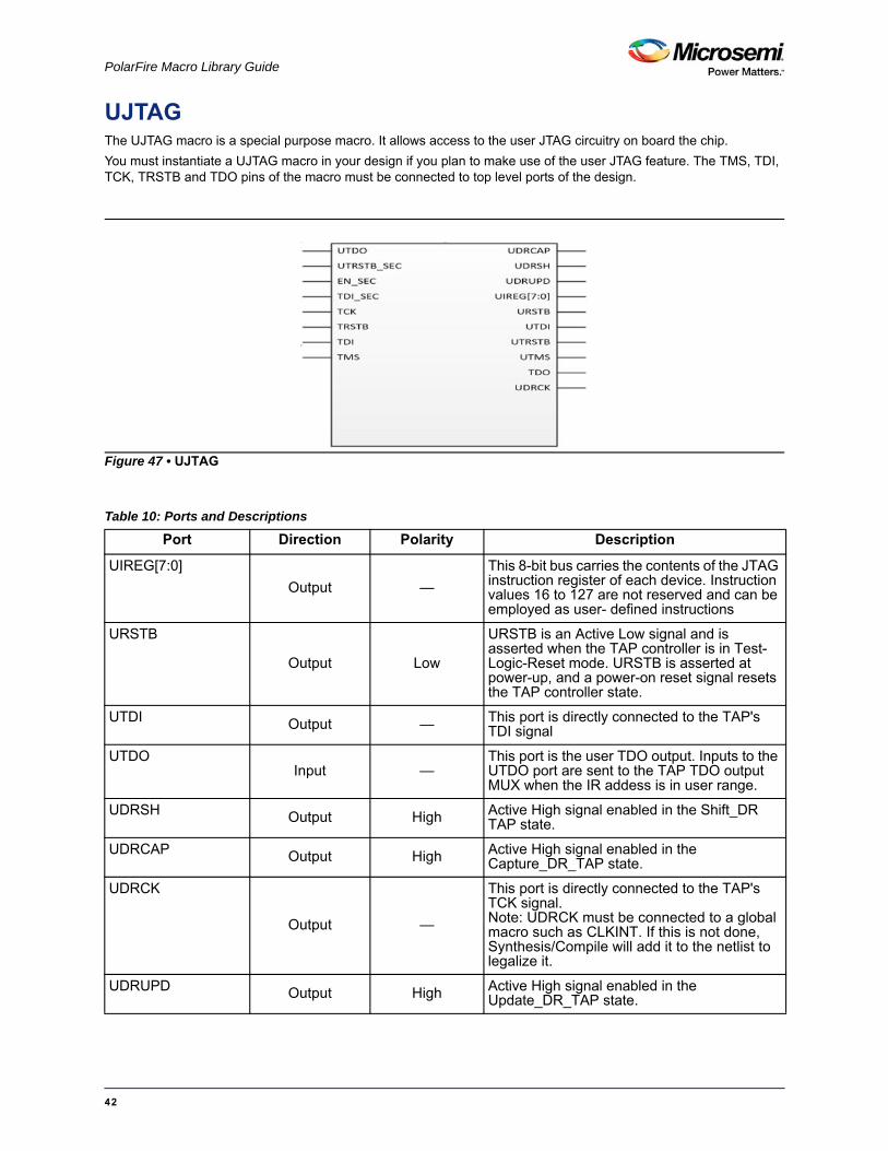
UJTAGThe UJTAG macro is a special purpose macro. It allows access to the user JTAG circuitry on board the chip.
You must instantiate a UJTAG macro in your design if you plan to make use of the user JTAG feature. The TMS, TDI, TCK, TRSTB and TDO pins of the macro must be connected to top level ports of the design.
Figure 47 • UJTAG
Table 10: Ports and Descriptions
Port Direction Polarity Description
UIREG[7:0]
Output —
This 8-bit bus carries the contents of the JTAG instruction register of each device. Instruction values 16 to 127 are not reserved and can be employed as user- defined instructions
URSTB
Output Low
URSTB is an Active Low signal and is asserted when the TAP controller is in Test- Logic-Reset mode. URSTB is asserted at power-up, and a power-on reset signal resets the TAP controller state.
UTDI Output — This port is directly connected to the TAP's TDI signal
UTDOInput —
This port is the user TDO output. Inputs to the UTDO port are sent to the TAP TDO output MUX when the IR addess is in user range.
UDRSH Output High Active High signal enabled in the Shift_DR TAP state.
UDRCAP Output High Active High signal enabled in the Capture_DR_TAP state.
UDRCK
Output —
This port is directly connected to the TAP's TCK signal.Note: UDRCK must be connected to a global macro such as CLKINT. If this is not done, Synthesis/Compile will add it to the netlist to legalize it.
UDRUPD Output High Active High signal enabled in the Update_DR_TAP state.
42

TCK
Input —
Test Clock. Serial input for JTAG boundary scan, ISP, and UJTAG. The TCK pin does not have an internal pull-up/pull- down resistor. Connect TCK to GND or +3.3 V through a resistor (500-1 KΩ) placed closed to the FPGA pin to prevent totem-pole current on the input buffer and TMS from entering into an undesired state.If JTAG is not used, connect it to GND.
TDIInput —
Test Data In. Serial input for JTAG boundary scan. There is an internal weak pull-up resistor on the TDI pin.
TDOOutput —
Test Data Out. Serial output for JTAG boundary scan. The TDO pin does not have an internal pull-up/pull-down resistor.
TMS
Input —
Test mode select. The TMS pin controls the use of the IEEE1532 boundary scan pins (TCK, TDI, TDO, and TRST). There is an internal weak pull- up resistor on the TMS pin.
TRSTB
Input Low
Test reset. The TRSTB pin is an active low input. It synchronously initializes (or resets) the boundary scan circuitry. There is an internal weak pull-up resistor on the TRSTB pin.To hold the JTAG in reset mode and prevent it from entering into undesired states in critical applications, connect TRSTB to GND through a 1 KΩ resistor (placed close to the FPGA pin).
Table 10: Ports and Descriptions (Continued)
Port Direction Polarity Description
43

PolarFire Macro Library Guide
UJTAG_SEC The UJTAG_SEC macro is a special purpose macro. It allows access to the user JTAG circuitry on board the chip.
You must instantiate a UJTAG_SEC macro in your design if you plan to make use of the user JTAG feature. The TMS, TDI, TCK, TRSTB and TDO pins of the macro must be connected to top level ports of the design.
Figure 48 • UJTAG_SEC
Table 11: Ports and Descriptions
Port Direction Polarity Description
UIREG[7:0]
Output —
This 8-bit bus carries the contents of the JTAG instruction register of each device. Instruction values 16 to 127 are not reserved and can be employed as user- defined instructions
URSTB
Output Low
URSTB is an Active Low signal and is asserted when the TAP controller is in Test- Logic-Reset mode. URSTB is asserted at power-up, and a power-on reset signal resets the TAP controller state.
UTDI Output — This port is directly connected to the TAP's TDI signal
UTDOInput —
This port is the user TDO output. Inputs to the UTDO port are sent to the TAP TDO output MUX when the IR addess is in user range.
44
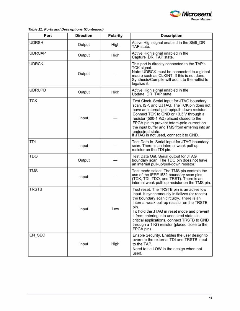
UDRSH Output High Active High signal enabled in the Shift_DR TAP state.
UDRCAP Output High Active High signal enabled in the Capture_DR_TAP state.
UDRCK
Output —
This port is directly connected to the TAP's TCK signal.Note: UDRCK must be connected to a global macro such as CLKINT. If this is not done, Synthesis/Compile will add it to the netlist to legalize it.
UDRUPD Output High Active High signal enabled in the Update_DR_TAP state.
TCK
Input —
Test Clock. Serial input for JTAG boundary scan, ISP, and UJTAG. The TCK pin does not have an internal pull-up/pull- down resistor. Connect TCK to GND or +3.3 V through a resistor (500-1 KΩ) placed closed to the FPGA pin to prevent totem-pole current on the input buffer and TMS from entering into an undesired state.If JTAG is not used, connect it to GND.
TDIInput —
Test Data In. Serial input for JTAG boundary scan. There is an internal weak pull-up resistor on the TDI pin.
TDOOutput —
Test Data Out. Serial output for JTAG boundary scan. The TDO pin does not have an internal pull-up/pull-down resistor.
TMS
Input —
Test mode select. The TMS pin controls the use of the IEEE1532 boundary scan pins (TCK, TDI, TDO, and TRST). There is an internal weak pull- up resistor on the TMS pin.
TRSTB
Input Low
Test reset. The TRSTB pin is an active low input. It synchronously initializes (or resets) the boundary scan circuitry. There is an internal weak pull-up resistor on the TRSTB pin.To hold the JTAG in reset mode and prevent it from entering into undesired states in critical applications, connect TRSTB to GND through a 1 KΩ resistor (placed close to the FPGA pin).
EN_SEC
Input High
Enable Security. Enables the user design to override the external TDI and TRSTB input to the TAP.Need to tie LOW in the design when not used.
Table 11: Ports and Descriptions (Continued)
Port Direction Polarity Description
45

PolarFire Macro Library Guide
TDI_SECInput —
TDI Security override. Overrides the external TDI input to the TAP when SEC_EN is HIGH.
TRSTB_SECInput Low
TRSTB Security override. Overrides the external TRSTB input to the TAP when SEC_EN is HIGH.
Table 11: Ports and Descriptions (Continued)
Port Direction Polarity Description
46

BIBUFBidirectional Buffer
Truth Table
BIBUF_DIFFBidirectional Buffer, Differential I/O
Truth Table
Figure 49 • BIBUF
Input Output
D, E, PAD PAD, Y
MODE E D PAD Y
OUTPUT 1 D D D
INPUT 0 X Z X
INPUT 0 X PAD PAD
Figure 50 • BIBUF_DIFF
Input Output
D, E, PADP, PADN PADP, PADN, Y
MODE E D PADP PADN Y
OUTPUT 1 0 0 1 0
OUTPUT 1 1 1 0 1
INPUT 0 X Z Z X
INPUT 0 X 0 0 X
INPUT 0 X 1 1 X
INPUT 0 X 0 1 0
INPUT 0 X 1 0 1
D PADE
Y
DPADPE
YPADN
47

PolarFire Macro Library Guide
INBUFInput Buffer
Truth Table
INBUF_DIFFInput Buffer, Differential I/O
Truth Table
Figure 51 • INBUF
Input Output
PAD Y
PAD Y
Z X
0 0
1 1
Figure 52 • INBUF_DIFF
Input Output
PADP, PADN Y
PADP PADN Y
Z Z X
0 0 X
1 1 X
0 1 0
1 0 1
YPAD
YPADP
PADN
48

OUTBUFOutput buffer
Truth Table
OUTBUF_DIFFOutput buffer, Differential I/O
Truth Table
Figure 53 • OUTBUF
Input Output
D PAD
D PAD
0 0
1 1
Figure 54 • OUTBUF_DIFF
Input Output
D PADP, PADN
D PADP PADN
0 0 1
1 1 0
PADD
PADPD
PADN
49

PolarFire Macro Library Guide
TRIBUFFTristate output buffer
Truth Table
TRIBUFF_DIFFTristate output buffer, Differential I/O
Truth Table
Figure 55 • TRIBUFF
Input Output
D, E PAD
D E PAD
X 0 Z
D 1 D
Figure 56 • TRIBUFF_DIFF
Input Output
D, E PADP, PADN
D E PADP PADN
X 0 Z Z
0 1 0 1
1 1 1 0
D PADE
DPADPE
PADN
50
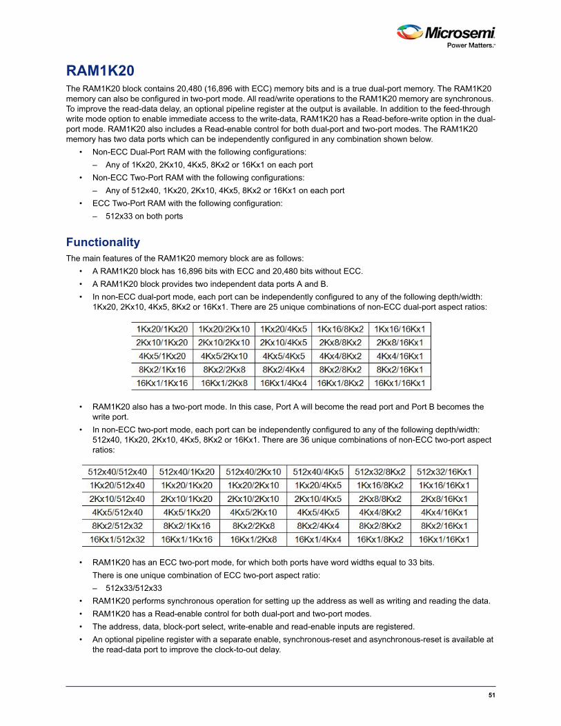
RAM1K20The RAM1K20 block contains 20,480 (16,896 with ECC) memory bits and is a true dual-port memory. The RAM1K20 memory can also be configured in two-port mode. All read/write operations to the RAM1K20 memory are synchronous. To improve the read-data delay, an optional pipeline register at the output is available. In addition to the feed-through write mode option to enable immediate access to the write-data, RAM1K20 has a Read-before-write option in the dual-port mode. RAM1K20 also includes a Read-enable control for both dual-port and two-port modes. The RAM1K20 memory has two data ports which can be independently configured in any combination shown below.
• Non-ECC Dual-Port RAM with the following configurations:
– Any of 1Kx20, 2Kx10, 4Kx5, 8Kx2 or 16Kx1 on each port
• Non-ECC Two-Port RAM with the following configurations:
– Any of 512x40, 1Kx20, 2Kx10, 4Kx5, 8Kx2 or 16Kx1 on each port
• ECC Two-Port RAM with the following configuration:
– 512x33 on both ports
FunctionalityThe main features of the RAM1K20 memory block are as follows:
• A RAM1K20 block has 16,896 bits with ECC and 20,480 bits without ECC.
• A RAM1K20 block provides two independent data ports A and B.
• In non-ECC dual-port mode, each port can be independently configured to any of the following depth/width: 1Kx20, 2Kx10, 4Kx5, 8Kx2 or 16Kx1. There are 25 unique combinations of non-ECC dual-port aspect ratios:
• RAM1K20 also has a two-port mode. In this case, Port A will become the read port and Port B becomes the write port.
• In non-ECC two-port mode, each port can be independently configured to any of the following depth/width: 512x40, 1Kx20, 2Kx10, 4Kx5, 8Kx2 or 16Kx1. There are 36 unique combinations of non-ECC two-port aspect ratios:
• RAM1K20 has an ECC two-port mode, for which both ports have word widths equal to 33 bits.
There is one unique combination of ECC two-port aspect ratio:
– 512x33/512x33
• RAM1K20 performs synchronous operation for setting up the address as well as writing and reading the data.
• RAM1K20 has a Read-enable control for both dual-port and two-port modes.
• The address, data, block-port select, write-enable and read-enable inputs are registered.
• An optional pipeline register with a separate enable, synchronous-reset and asynchronous-reset is available at the read-data port to improve the clock-to-out delay.
51

PolarFire Macro Library Guide
• There is an independent clock for each port. The memory is triggered at the rising edge of the clock.
• The true dual-port mode supports an optional Read-before-write mode or a feed-through write mode, where the write-data also appears on the corresponding read-data port.
• Read from both ports at the same location is allowed.
• Read and write on the same location at the same time results in unknown data to be read.
There is no collision prevention or detection. However, correct data is expected to be written into the memory.
• When ECC is enabled, each port of the RAM1K20 memory can raise flags to indicate single-bit- correct and double-bit-detect.
Figure 57 shows a simplified block diagram of the RAM1K20 memory block. The simplified block illustrates the two independent data ports, ECC, the read-data pipeline registers, read-before-write selection, and the feed-through multiplexors.
Figure 57 • Simplified Block Diagram of RAM1K20
52

Port List
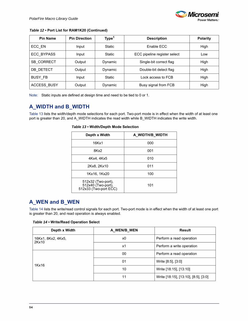
Table 12 • Port List for RAM1K20
Pin Name Pin Direction Type1 Description Polarity
A_ADDR[13:0] Input Dynamic Port A address
A_BLK_EN[2:0] Input Dynamic Port A block selects High
A_CLK Input Dynamic Port A clock Rising
A_DIN[19:0] Input Dynamic Port A write-data
A_DOUT[19:0] Output Dynamic Port A read-data
A_WEN[1:0] Input Dynamic Port A write-enables (per byte) High
A_REN Input Dynamic Port A read-enable High
A_WIDTH[2:0] Input Static Port A width/depth mode select
A_WMODE[1:0] Input Static Port A Read-before-write and Feed-through write selects High
A_BYPASS Input Static Port A pipeline register select Low
A_DOUT_EN Input Dynamic Port A pipeline register enable High
A_DOUT_SRST_N Input Dynamic Port A pipeline register synchronous-reset Low
A_DOUT_ARST_N Input Dynamic Port A pipeline register asynchronous-reset Low
B_ADDR[13:0] Input Dynamic Port B address
B_BLK_EN[2:0] Input Dynamic Port B block selects High
B_CLK Input Dynamic Port B clock Rising
B_DIN[19:0] Input Dynamic Port B write-data
B_DOUT[19:0] Dynamic Port B read-data
B_WEN[1:0] Input Dynamic Port B write-enables (per byte) High
B_REN Input Dynamic Port B read-enable High
B_WIDTH[2:0] Input Static Port B width/depth mode select
B_WMODE[1:0] Input Static Port B Read-before-write and Feed-through write selects High
B_BYPASS Input Static Port B pipeline register select Low
B_DOUT_EN Input Dynamic Port B pipeline register enable High
B_DOUT_SRST_N Input Dynamic Port B pipeline register synchronous-reset Low
B_DOUT_ARST_N Input Dynamic Port B pipeline register asynchronous-reset Low
53
PolarFire Macro Library Guide
Note: Static inputs are defined at design time and need to be tied to 0 or 1.
A_WIDTH and B_WIDTHTable 13 lists the width/depth mode selections for each port. Two-port mode is in effect when the width of at least one port is greater than 20, and A_WIDTH indicates the read width while B_WIDTH indicates the write width.
A_WEN and B_WENTable 14 lists the write/read control signals for each port. Two-port mode is in effect when the width of at least one port is greater than 20, and read operation is always enabled.
ECC_EN Input Static Enable ECC High
ECC_BYPASS Input Static ECC pipeline register select Low
SB_CORRECT Output Dynamic Single-bit correct flag High
DB_DETECT Output Dynamic Double-bit detect flag High
BUSY_FB Input Static Lock access to FCB High
ACCESS_BUSY Output Dynamic Busy signal from FCB High
Table 13 • Width/Depth Mode Selection
Depth x Width A_WIDTH/B_WIDTH
16Kx1 000
8Kx2 001
4Kx4, 4Kx5 010
2Kx8, 2Kx10 011
1Kx16, 1Kx20 100
512x32 (Two-port),512x40 (Two-port),
512x33 (Two-port ECC)101
Table 14 • Write/Read Operation Select
Depth x Width A_WEN/B_WEN Result
16Kx1, 8Kx2, 4Kx5,2Kx10
x0 Perform a read operation
x1 Perform a write operation
1Kx16
00 Perform a read operation
01 Write [8:5], [3:0]
10 Write [18:15], [13:10]
11 Write [18:15], [13:10], [8:5], [3:0]
Table 12 • Port List for RAM1K20 (Continued)
Pin Name Pin Direction Type1 Description Polarity
54
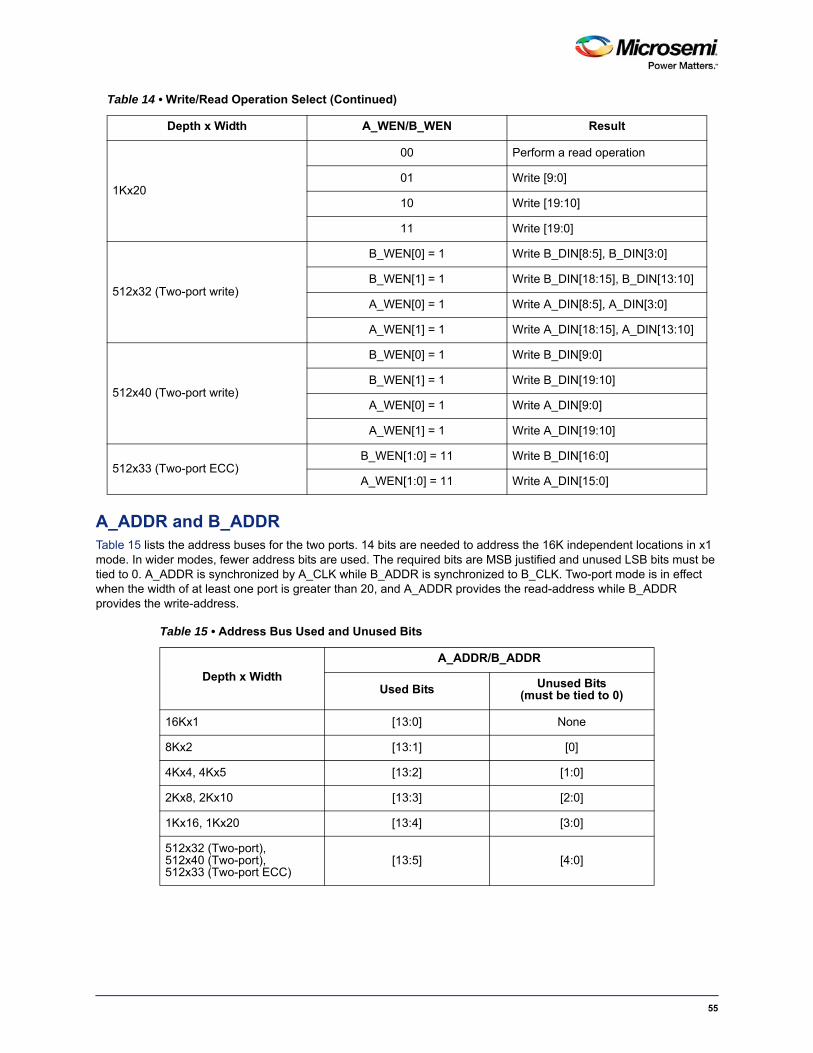
A_ADDR and B_ADDRTable 15 lists the address buses for the two ports. 14 bits are needed to address the 16K independent locations in x1 mode. In wider modes, fewer address bits are used. The required bits are MSB justified and unused LSB bits must be tied to 0. A_ADDR is synchronized by A_CLK while B_ADDR is synchronized to B_CLK. Two-port mode is in effect when the width of at least one port is greater than 20, and A_ADDR provides the read-address while B_ADDR provides the write-address.
1Kx20
00 Perform a read operation
01 Write [9:0]
10 Write [19:10]
11 Write [19:0]
512x32 (Two-port write)
B_WEN[0] = 1 Write B_DIN[8:5], B_DIN[3:0]
B_WEN[1] = 1 Write B_DIN[18:15], B_DIN[13:10]
A_WEN[0] = 1 Write A_DIN[8:5], A_DIN[3:0]
A_WEN[1] = 1 Write A_DIN[18:15], A_DIN[13:10]
512x40 (Two-port write)
B_WEN[0] = 1 Write B_DIN[9:0]
B_WEN[1] = 1 Write B_DIN[19:10]
A_WEN[0] = 1 Write A_DIN[9:0]
A_WEN[1] = 1 Write A_DIN[19:10]
512x33 (Two-port ECC)B_WEN[1:0] = 11 Write B_DIN[16:0]
A_WEN[1:0] = 11 Write A_DIN[15:0]
Table 15 • Address Bus Used and Unused Bits
Depth x Width
A_ADDR/B_ADDR
Used Bits Unused Bits(must be tied to 0)
16Kx1 [13:0] None
8Kx2 [13:1] [0]
4Kx4, 4Kx5 [13:2] [1:0]
2Kx8, 2Kx10 [13:3] [2:0]
1Kx16, 1Kx20 [13:4] [3:0]
512x32 (Two-port),512x40 (Two-port),512x33 (Two-port ECC)
[13:5] [4:0]
Table 14 • Write/Read Operation Select (Continued)
Depth x Width A_WEN/B_WEN Result
55

PolarFire Macro Library Guide
A_DIN and B_DINTable 5 lists the data input buses for the two ports. The required bits are LSB justified and unused MSB bits must be tied to 0. Two-port mode is in effect when the width of at least one port is greater than 20, and A_DIN provides the MSB of the write-data while B_DIN provides the LSB of the write- data.
A_DOUT and B_DOUTTable 17 lists the data output buses for the two ports. The required bits are LSB justified. Two-port mode is in effect when the width of at least one port is greater than 20, and A_DOUT provides the MSB of the read-data while B_DOUT provides the LSB of the read-data..
Table 16 • Data Input Buses Used and Unused Bits
Depth x Width
A_DIN/B_DIN
Used Bits Unused Bits(must be tied to 0)
16Kx1 [0] [19:1]
8Kx2 [1:0] [19:2]
4Kx4 [3:0] [19:4]
4Kx5 [4:0] [19:5]
2Kx8 [8:5] is [7:4][3:0] is [3:0]
[19:9][4]
2Kx10 [9:0] [19:10]
1Kx16
[18:15] is [15:12][13:10] is [11:8]
[8:5] is [7:4][3:0] is [3:0]
[19][14][9][4]
1Kx20 [19:0] None
512x32 (Two-port write)
A_DIN[18:15] is [31:28] A_DIN[13:10] is [27:24] A_DIN[8:5] is [23:20] A_DIN[3:0] is [19:16]
B_DIN[18:15] is [15:12 B_DIN[13:10] is [11:8]
B_DIN[8:5] is [7:4]B_DIN[3:0] is [3:0]
A_DIN[19]A_DIN[14]A_DIN[9]A_DIN[4]
B_DIN[19]B_DIN[14]B_DIN[9]B_DIN[4]
512x40 (Two-port write) A_DIN[19:0] is [39:20] B_DIN[19:0] is [19:0 ] None
512x33 (Two-port ECC) A_DIN[15:0] is [32:17] B_DIN[16:0] is [16:0 ]
A_DIN[19:16]B_DIN[19:17]
Table 17 • Data Output Buses Used and Unused Bits
Depth x Width
A_DOUT/B_DOUT
Used Bits Unused Bits(must be tied to 0)
16Kx1 [0] [19:1]
8Kx2 [1:0] [19:2]
56

A_BLK_EN and B_BLK_ENTable 18 lists the block-port select control signals for the two ports. A_BLK is synchronized by A_CLK while B_BLK is synchronized to B_CLK. Two-port mode is in effect when the width of at least one port is greater than 20, and A_BLK_EN controls the read operation while B_BLK_EN controls the write operation.
4Kx4 [3:0] [19:4]
4Kx5 [4:0] [19:5]
2Kx8 [8:5] is [7:4][3:0] is [3:0]
[19:9][4]
2Kx10 [9:0] [19:10]
1Kx16
[18:15] is [15:12][13:10] is [11:8]
[8:5] is [7:4][3:0] is [3:0]
[19][14][9][4]
1Kx20 [19:0] None
512x32 (Two-port write)
A_DIN[18:15] is [31:28] A_DIN[13:10] is [27:24] A_DIN[8:5] is [23:20] A_DIN[3:0] is [19:16]
B_DIN[18:15] is [15:12 B_DIN[13:10] is [11:8]
B_DIN[8:5] is [7:4]B_DIN[3:0] is [3:0]
A_DIN[19]A_DIN[14]A_DIN[9]A_DIN[4]
B_DIN[19]B_DIN[14]B_DIN[9]B_DIN[4]
512x40 (Two-port write) A_DOUT[19:0] is [39:20] B_DOUT[19:0] is [19:0 ] None
512x33 (Two-port ECC) A_DOUT15:0] is [32:17] B_DOUT[16:0] is [16:0 ]
A_DOUT[19:16]B_DOUT[19:17]
Table 18 • Block-port Select
Block-portSelect Signal Value Result
A_BLK_EN[2:0] 111 Perform read or write operation on Port A, unless the width is greater than 20 and a read is performed from both ports A and B.
A_BLK_EN[2:0] Any one bit is 0No operation in memory from Port A. Port A read-data will be forced to 0. If the width is greater than 20, the read-data from both ports A and B will be forced to 0.
B_BLK_EN[2:0] 111 Perform read or write operation on Port B, unless the width is greater than 20 and a write is performed to both ports A and B.
B_BLK_EN[2:0] Any one bit is 0No operation in memory from Port B. Port B read-data will be forced to 0, unless the width is greater than 20 and write operation to both ports A and B is gated.
Table 17 • Data Output Buses Used and Unused Bits (Continued)
Depth x Width
A_DOUT/B_DOUT
Used Bits Unused Bits(must be tied to 0)
57

PolarFire Macro Library Guide
A_WMODE and B_WMODEIn true dual-port write mode, each port has a feed-through write or read-before-write option.
• Logic 00 = Read-data port holds the previous value.
• Logic 01 = Feed-through, i.e. write-data appears on the corresponding read-data port. This setting is invalid when the width of at least one port is greater than 20 and the two-port mode is in effect.
• Logic 10 = Read-before-write, i.e. previous content of the memory appears on the corresponding read-data port before it is overwritten. This setting is invalid when the width of at least one port is greater than 20 and the two-port mode is in effect.
A_CLK and B_CLKAll signals in ports A and B are synchronous to the corresponding port clock. All address, data, block- port select, write-enable and read-enable inputs must be set up before the rising edge of the clock. The read or write operation begins with the rising edge. Two-port mode is in effect when the width of at least one port is greater than 20, and A_CLK provides the read clock while B_CLK provides the write clock.
A_REN and B_RENEnables read operation from the memory on the corresponding port. Two-port read mode is in effect when the width of port A is greater than 20, and A_REN controls the read operation.
Read-data Pipeline Register Control SignalsA_BYPASS and B_BYPASS A_DOUT_EN and B_DOUT_EN A_DOUT_SRST_N and B_DOUT_SRST_N A_DOUT_ARST_N and B_DOUT_ARST_N
Two-port mode is in effect when the width of at least one port is greater than 20, and the A_DOUT register signals control both the MSB and LSB of the read-data, and the B_DOUT register signals are “don’t-cares”.
Table 19 describes the functionality of the control signals on the A_DOUT and B_DOUT pipeline registers.
ECC_EN and ECC_BYPASSECC operation is only allowed in Two-port mode and the width of both ports is greater than 20.
• ECC_EN = 0: Disable ECC.
• ECC_EN = 1, ECC_BYPASS= 0: Enable ECC Pipelined.
– ECC Pipelined mode inserts an additional clock cycle to Read-data.
– In addition, Write-feed-thru and Read-before-write modes add another clock cycle to Read- data.
• ECC_EN = 1, ECC_BYPASS= 1: Enable ECC Non-pipelined.
Table 19 • Truth Table for A_DOUT and B_DOUT Registers
ARST_N _BYPASS _CLK _EN _SRST_N D Qn+1
0 X X X X X 0
1 0 Not rising X X X Qn
1 0 ↑ 0 X X Qn
1 0 ↑ 1 0 X 0
1 0 ↑ 1 1 D D
1 1 X X X D D
58

SB_CORRECT and DB_DETECTError detection and correction flags become available when ECC operation is enabled in Two-port mode and the width of both ports is greater than 20. Table 20 describes the functionality of the error detection and correction flags.
BUSY_FBControl signal, when 1 locks the entire RAM1K20 memory from being accessed by the FCB.
ACCESS_BUSYThis output indicates that the RAM1K20 memory is being accessed by the FCB.
Table 20 • Error detection and correction flags
DB_DETECT SB_CORRECT Flag
0 0 No errors have been detected.
0 1 A single bit error has been detected and corrected in the data output.
1 1 Multiple bit errors have been detected, but have not been corrected.
59

PolarFire Macro Library Guide
RAM64x12The RAM64x12 block contains 768 memory bits and is a two-port memory providing one write port and one read port. Write operations to the RAM64x12 memory are synchronous. Read operations can be asynchronous or synchronous for setting up the address and reading out the data. Enabling synchronous operation at the read-address port improves setup timing for the read-address and its enable signals. Enabling synchronous operation at the read-data port improves clock-to-out delay. Each data port on the RAM64x12 memory is configured to a fixed configuration of 64x12.
FunctionalityThe main features of the RAM64x12 memory block are as follows.
• There is one read-data port and one write-data port.
• Both read-data and write-data ports are configured to 64x12.
• The write operation is always synchronous. The write-address, write-data and write-enable inputs are registered.
• Setting up the read-address can be synchronous or asynchronous. The read-address registers have an independent enable, synchronous-load and asynchronous-load for synchronous mode operation, which can be bypassed for asynchronous mode operation.
• The read-data pipeline registers have an independent enable, synchronous-load and asynchronous-load for pipeline mode operation, which can be bypassed for asynchronous mode operation.
• Therefore, there are four read operation modes:
– Synchronous read-address without read-data pipeline registers (sync-async)
– Synchronous read-address with read-data pipeline registers (sync-sync)
– Asynchronous read-address with read-data pipeline registers (async-sync)
– Asynchronous read-address without read-data pipeline registers (async-async)
• There is an independent clock for each port. The memory will be triggered at the rising edge of the clock.
• Read and write on the same location at the same time results in unknown data to be read.
There is no collision prevention or detection. However, correct data is expected to be written into the memory.
Figure 58 • Simplified Block Diagram of RAM64x12
60

Port ListTable 21 gives the port descriptions.
Table 21 • Port List for RAM1K20
Pin Name Pin Direction Type1 Description Polarity
W_EN Input Dynamic Write port enable High
W_CLK Input Dynamic
Write clock. All write-address, write-data and write-enable inputs must be set up before the rising edge of the clock. The write operation begins with the rising edge.
Rising
W_ADDR[5:0] Input Dynamic Write address
W_DATA[11:0] Input Dynamic Write-data
BLK_EN Input Dynamic
Read port block select. When High, read operation is performed. When Low, read-data will be forced to zero. BLK_EN signal is registered through R_CLK when R_ADDR_BYPASS is Low.
High
R_CLK Input Dynamic
Read registers clock. All read-address, block- port select and read-enable inputs must be set up before the rising edge of the clock. The read operation begins with the rising edge.
Rising
R_ADDR[5:0] Input Dynamic Read-address
R_ADDR_BYPASS Input Static Read-address and BLK_EN register select Low
R_ADDR_EN Input Dynamic Read-address register enable High
R_ADDR_SL_N Input Dynamic Read-address register synchronous load Low
R_ADDR_SD Input Static Read-address register synchronous load data High
R_ADDR_AL_N Input Dynamic Read-address register asynchronous load Low
R_ADDR_AD_N Input Static Read-address register asynchronous load data Low
R_DATA[11:0] Output Dynamic Read-data
R_DATA_BYPASS Input Static Read-data pipeline register select Low
R_DATA_EN Input Dynamic Read-data pipeline register enable High
R_DATA_SL_N Input Dynamic Read-data pipeline register synchronous load Low
R_DATA_SD Input Static Read-data pipeline register synchronous load data High
R_DATA_AL_N Input Dynamic Read-data pipeline register asynchronous load Low
61

PolarFire Macro Library Guide
Note: Static inputs are defined at design time and need to be tied to 0 or 1.
Read-address and Read-data Pipeline Register Control SignalsTable 22 describes the functionality of the control signals on the R_ADDR and R_DATA registers.
R_DATA_AD_N Input Dynamic Read-data pipeline register asynchronous load data Low
BUSY_FB Input Static Lock access to FCB High
ACCESS_BUSY Output Dynamic Busy signal from FCB High
Table 22 • Truth Table for R_ADDR and R_DATA Registers
_AL_N _AD_N _BYPASS _CLK _EN _SL_N _SD D Qn+1
0 ADn X X X X X X !ADn
1 X 0 Not rising X X X X Qn
1 X 0 ↑ 0 X X X Qn
1 X 0 ↑ 1 0 SD X SD
1 X 0 ↑ 1 1 X D D
1 X 1 X X X X D D
Table 21 • Port List for RAM1K20 (Continued)
Pin Name Pin Direction Type1 Description Polarity
62
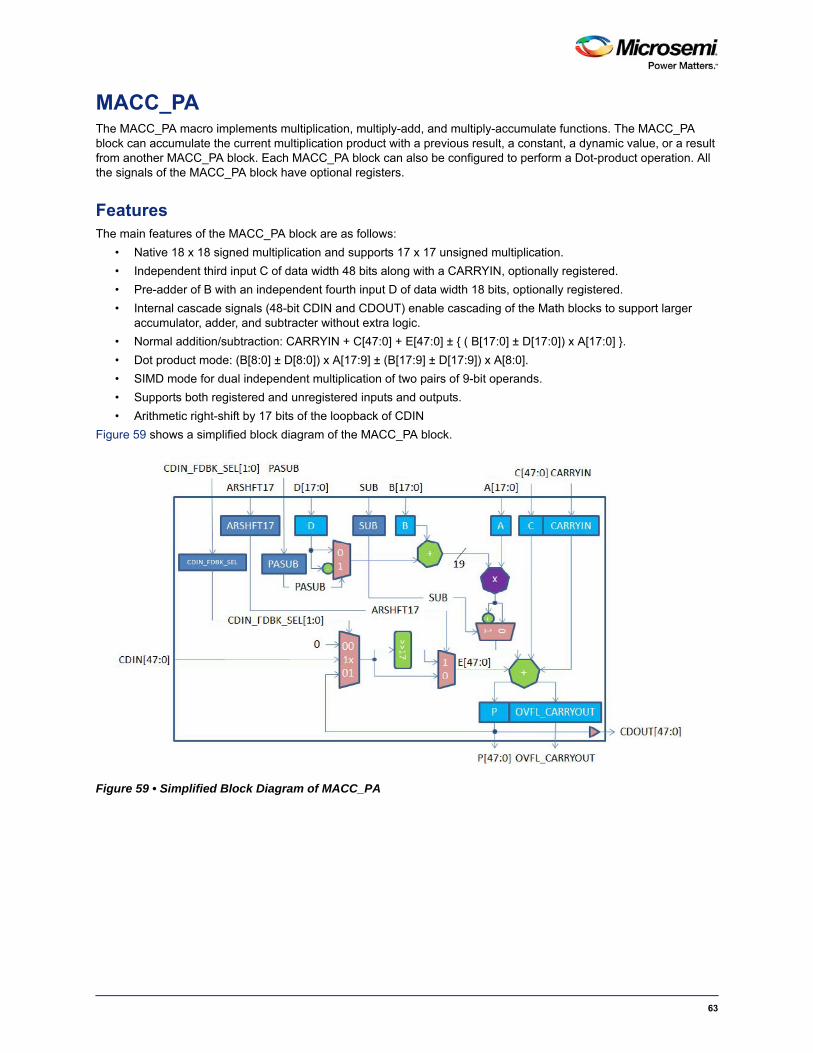
MACC_PAThe MACC_PA macro implements multiplication, multiply-add, and multiply-accumulate functions. The MACC_PA block can accumulate the current multiplication product with a previous result, a constant, a dynamic value, or a result from another MACC_PA block. Each MACC_PA block can also be configured to perform a Dot-product operation. All the signals of the MACC_PA block have optional registers.
FeaturesThe main features of the MACC_PA block are as follows:
• Native 18 x 18 signed multiplication and supports 17 x 17 unsigned multiplication.
• Independent third input C of data width 48 bits along with a CARRYIN, optionally registered.
• Pre-adder of B with an independent fourth input D of data width 18 bits, optionally registered.
• Internal cascade signals (48-bit CDIN and CDOUT) enable cascading of the Math blocks to support larger accumulator, adder, and subtracter without extra logic.
• Normal addition/subtraction: CARRYIN + C[47:0] + E[47:0] ± ( B[17:0] ± D[17:0]) x A[17:0] .
• Dot product mode: (B[8:0] ± D[8:0]) x A[17:9] ± (B[17:9] ± D[17:9]) x A[8:0].
• SIMD mode for dual independent multiplication of two pairs of 9-bit operands.
• Supports both registered and unregistered inputs and outputs.
• Arithmetic right-shift by 17 bits of the loopback of CDIN
Figure 59 shows a simplified block diagram of the MACC_PA block.
Figure 59 • Simplified Block Diagram of MACC_PA
63
PolarFire Macro Library Guide
Port List
Table 23 • MACC_PA Pin Descriptions
Port Name Direction Type Polarity Description
DOTP Input Static High
Dot-product mode.When DOTP = 1, MACC_PA block performs Dot- product of two pairs of 9-bit operands.• SIMD must not be 1.• C[8:0] must be connected to CARRYIN.
SIMD Input Static High
SIMD mode.When SIMD = 1, MACC_PA block performs dualindependent multiplication of two pairs of 9-bitoperands.• DOTP must not be 1.• ARSHFT17 must be 0.• D[8:0] must be 0.• C[17:0] must be 0.• E[17:0] must be 0. Refer to Table 24 to see how operand E is obtained from P, CDIN or 0.
OVFL_CARRYOUT_SEL Input Static High
Generate OVERFLOW or CARRYOUT with result P.• OVERFLOW when OVFL_CARRYOUT_SEL = 0• CARRYOUT when OVFL_CARRYOUT_SEL = 1
CLK Input Dynamic Rising edge
Clock for A, B, C, CARRYIN, D, P, OVFL_CARRYOUT, ARSHFT17, CDIN_FDBK_SEL, PASUB and SUB registers.
AL_N Input Dynamic Low
Asynchronous load for A, B, P, OVFL_CARRYOUT, ARSHFT17, CDIN_FDBK_SEL, PASUB and SUB registers. Connect to 1, if none are registered.When asserted, A, B, P and OVFL_CARRYOUTregisters are loaded with zero, while theARSHFT17, CDIN_FDBK_SEL, PASUB and SUBregisters are loaded with the complementaryvalue of the respective _AD_N.
A[17:0] Input Dynamic High Input data A.
A_BYPASS Input Static HighBypass data A registers. Connect to 1, if not registered. See Table 28.
A_SRST_N Input Dynamic LowSynchronous reset for data A registers. Connect to1, if not registered. See Table 28.
A_EN Input Dynamic HighEnable for data A registers. Connect to 1, if not registered. See Table 28.
B[17:0] Input Dynamic High Input data B to Pre-adder with data D.
B_BYPASS Input Static HighBypass data B registers. Connect to 1, if not registered. See Table 28.
B_SRST_N Input Dynamic LowSynchronous reset for data B registers. Connect to 1, if not registered. See Table 28.
64

B_EN Input Dynamic HighEnable for data B registers. Connect to 1, if not registered. See Table 28.
D[17:0] Input Dynamic HighInput data D to Pre-adder with data B. When SIMD = 1, connect D[8:0] to 0.
D_BYPASS Input Static High Bypass data D registers. Connect to 1, if not registered. See Table 29.
D_ARST_N Input Dynamic LowAsynchronous reset for data D registers. Connect to 1, if not registered. See Table 29.
D_SRST_N Input Dynamic LowSynchronous reset for data D registers. Connect to 1, if not registered. See Table 29.
D_EN Input Dynamic HighEnable for data D registers. Connect to 1, if not registered. See Table 29.
CARRYIN Input Dynamic High CARRYIN for input data C.
C[47:0] Input Dynamic High
Input data C.When DOTP = 1, connect C[8:0] to CARRYIN. When SIMD = 1, connect C[8:0] to 0.
C_BYPASS Input Static HighBypass CARRYIN and C registers. Connect to 1, if not registered. See Table 29.
C_ARST_N Input Dynamic LowAsynchronous reset for CARRYIN and C registers. Connect to 1, if not registered. See Table 29.
C_SRST_N Input Dynamic LowSynchronous reset for CARRYIN and C registers. Connect to 1, if not registered. See Table 29.
C_EN Input Dynamic HighEnable for CARRYIN and C registers. Connect to 1, if not registered. See Table 29.
CDIN[47:0] Input Cascade High
Cascaded input for operand E.The entire bus must be driven by an entireCDOUT of another MACC_PA orMACC_PA_BC_ROM block. In Dot-product mode,the driving CDOUT must also be generated by aMACC_PA or MACC_PA_BC_ROM block in Dot-product mode. Refer to Table 24 to see how CDIN is propagated to operand E.
P[47:0] Output High Result data. See Table 25.
OVFL_CARRYOUT Output High OVERFLOW or CARRYOUT. See Table 26.
P_BYPASS Input Static HighBypass P and OVFL_CARRYOUT registers. Connect to 1, if not registered. See Table 28.
P_SRST_N Input Dynamic LowSynchronous reset for P and OVFL_CARRYOUT registers. Connect to 1, if not registered. See Table 28
P_EN Input Dynamic HighEnable for P and OVFL_CARRYOUT registers. Connect to 1, if not registered. See Table 28.
Table 23 • MACC_PA Pin Descriptions (Continued)
65
PolarFire Macro Library Guide
CDOUT[47:0] Output Cascade High
Cascade output of result P. See Table 25.Value of CDOUT is the same as P. The entire busmust either be dangling or drive an entire CDIN ofanother MACC_PA or MACC_PA_BC_ROM block incascaded mode.
PASUB Input Dynamic High Subtract operation for Pre-adder of B and D.
PASUB_BYPASS Input Static High Bypass PASUB register. Connect to 1, if not registered. See Table 27.
PASUB_AD_N Input Static LowAsynchronous load data for PASUB register. See Table 27.
PASUB_SL_N Input Dynamic Low Synchronous load for PASUB register. Connect to1, if not registered. See Table 27.
PASUB_SD_N Input Static Low Synchronous load data for PASUB register. SeeTable 27.
PASUB_EN Input Dynamic High Enable for PASUB register. Connect to 1, if not registered. See Table 27.
CDIN_FDBK_SEL[1:0]
Input Dynamic High Select CDIN, P or 0 for operand E. See Table 24.
CDIN_FDBK_SEL_BYPASS
Input Static High Bypass CDIN_FDBK_SEL register. Connect to 1, if not registered. See Table 27.
CDIN_FDBK_SEL_AD_N[1:0]
Input Static Low Asynchronous load data for CDIN_FDBK_SELregister. See Table 27.
CDIN_FDBK_SEL_SL_N
Input Dynamic Low Synchronous load for CDIN_FDBK_SEL register. Connect to 1, if not registered. See Table 27.
CDIN_FDBK_SEL_SD_N[1:0]
Input Static Low Synchronous load data for CDIN_FDBK_SELregister. See Table 27.
CDIN_FDBK_SEL_EN
Input Dynamic High Enable for CDIN_FDBK_SEL register. Connect to 1, if not registered. See Table 27.
ARSHFT17 Input Dynamic High
Arithmetic right-shift for operand E.When asserted, a 17-bit arithmetic right-shift is performed on operand E. Refer to Table 24 to see how operand E is obtained from P, CDIN or 0. When SIMD = 1, ARSHFT17 must be 0.
ARSHFT17_BYPASS
Input Static High Bypass ARSHFT17 register. Connect to 1, if not registered. See Table 27.
ARSHFT17_AD_N Input Static Low Asynchronous load data for ARSHFT17 register. See Table 27.
ARSHFT17_SL_N Input Dynamic Low Synchronous load for ARSHFT17 register. Connect to 1, if not registered. See Table 27.
ARSHFT17_SD_N Input Static Low Synchronous load data for ARSHFT17 register. See Table 27.
ARSHFT17_EN Input Dynamic High Enable for ARSHFT17 register. Connect to 1, if not registered. See Table 27.
SUB Input Dynamic High Subtract operation.
Table 23 • MACC_PA Pin Descriptions (Continued)
66

Note: Static inputs are defined at design time and need to be tied to 0 or 1.
SUB_BYPASS Input Static High Bypass SUB register. Connect to 1, if not registered. See Table 27.
SUB_AD_N Input Static Low Asynchronous load data for SUB register. SeeTable 27
SUB_SL_N Input Dynamic Low Synchronous load for SUB register. Connect to 1, if not registered. See Table 27.
SUB_SD_N Input Static Low Synchronous load data for SUB register. SeeTable 27.
SUB_EN Input Dynamic High Enable for SUB register. Connect to 1, if not registered. See Table 27.
Table 24 • Truth Table—Propagating Data to Operand E
CDIN_FDBK_SEL[1] CDIN_FDBK_SEL[0] ARSHFT17 Operand E
0 0 X 48'b0
0 1 0 P[47:0]
0 1 1 17P[47],P[47:17]
1 X 0 CDIN[47:0]
1 X 1 17CDIN[47],CDIN[47:17]
Table 25 • Truth Table - Computation of Result P and CDOUT
SIMD DOTP SUB PASUB Result P and CDOUT
0 0 0 0 CARRYIN + C[47:0] + E[47:0] + (B[17:0] + D[17:0]) x A[17:0]
0 0 0 1 CARRYIN + C[47:0] + E[47:0] + (B[17:0] - D[17:0]) x A[17:0]
0 0 1 0 CARRYIN + C[47:0] + E[47:0] - (B[17:0] + D[17:0]) x A[17:0]
0 0 1 1 CARRYIN + C[47:0] + E[47:0] - (B[17:0] - D[17:0]) x A[17:0]
0 1 0 0CARRYIN + C[47:0] + E[47:0] + (B[8:0] + D[8:0]) x A[17:9] + (B[17:9] + D[17:9]) x A[8:0] x 29
0 1 0 1CARRYIN + C[47:0] + E[47:0] + (B[8:0] - D[8:0]) x A[17:9] + (B[17:9] - D[17:9]) x A[8:0] x 29
0 1 1 0CARRYIN + C[47:0] + E[47:0] + (B[8:0] + D[8:0]) x A[17:9] - (B[17:9] + D[17:9]) x A[8:0] x 29
0 1 1 1CARRYIN + C[47:0] + E[47:0] + (B[8:0] - D[8:0]) x A[17:9] - (B[17:9] - D[17:9]) x A[8:0] x 29
1 0 0 0P[17:0] = CARRYIN + B[8:0] x A[8:0] P[47:18] = C[47:18] + E[47:18] + (B[17:9] + D[17:9]) x A[17:9]
Table 23 • MACC_PA Pin Descriptions (Continued)
67

PolarFire Macro Library Guide
Note: SUM[49:0] is defined similarly to P[47:0] as shown in Table 25, except that SUM is a 50-bit quantity so that nooverflow can occur. SUM[48] is the carry out bit of a 48-bit final adder producing P[47:0].
1 0 0 1P[17:0] = CARRYIN + B[8:0] x A[8:0] P[47:18] = C[47:18] + E[47:18] + (B[17:9] - D[17:9]) x A[17:9]
1 0 1 0P[17:0] = CARRYIN + B[8:0] x A[8:0] P[47:18] = C[47:18] + E[47:18] - (B[17:9] + D[17:9]) x A[17:9]
1 0 1 1P[17:0] = CARRYIN + B[8:0] x A[8:0] P[47:18] = C[47:18] + E[47:18] - (B[17:9] - D[17:9]) x A[17:9]
Table 26 • Truth Table - Computation of OVFL_CARRYOUT
OVFL_CARRYOUT_SEL OVFL_CARRYOUT Description
0 (SUM[49] ^ SUM[48]) | (SUM[48] ^ SUM[47]) True if overflow or underflow occurred.
1 C[47] ^ E[47] ^ SUM[48] A signal that can be used to extend the final adder in the fabric.
Table 27 • Truth Table for Control Registers ARSHFT17, CDIN_FDBK_SEL, PASUB and SUB
AL_ _AD_N _BYPASS CLK _EN _SL_N _SD_N D Qn+1
0 AD_N 0 X X X X X !AD_
1 X 0 Not rising X X X X Qn
1 X 0 ↑ 0 X X X Qn
1 X 0 ↑ 1 0 SD_N X !SD_
1 X 0 ↑ 1 1 X D D
X X 1 X 0 X X X Qn
X X 1 X 1 0 SD_N X !SD_
X X 1 X 1 1 X D D
Table 28 • Truth Table - Data Registers A, B, P and OVFL_CARRYOUT
AL_N _BYPASS CLK _EN _SRST_N D Qn+1
0 0 X X X X 0
1 0 Not rising X X X Qn
1 0 ↑ 0 X X Qn
1 0 ↑ 1 0 X 0
1 0 ↑ 1 1 D D
Table 25 • Truth Table - Computation of Result P and CDOUT (Continued)
68

MACC_PA_BC_ROMThe MACC_PA_BC_ROM macro extends the functionality of the MACC_PA macro to provide a 16x18 ROM at the A input along with a pipelined output of B for cascading.
FeaturesThe additional features of the MACC_PA_BC_ROM block are as follows:
• Selection of the A input from a 16x18 ROM.
• Additional pipelining of the B input for cascading to the next Math block or output to the fabric.
• Due to routing bandwidth limitations, either result P or B2 output can be used in the same MACC_PA_BC_ROM block.
Figure 60 shows a simplified block diagram of the MACC_PA_BC_ROM block.
X 1 X 0 X X Qn
X 1 X 1 0 X 0
X 1 X 1 1 D D
Table 29 • Truth Table - Data Registers C, CARRYIN and D
_ARST_N _BYPASS CLK _EN _SRST_N D Qn+1
0 0 X X X X 0
1 0 Not rising X X X Qn
1 0 ↑ 0 X X Qn
1 0 ↑ 1 0 X 0
1 0 ↑ 1 1 D D
X 1 X 0 X X Qn
X 1 X 1 0 X 0
X 1 X 1 1 D D
Table 28 • Truth Table - Data Registers A, B, P and OVFL_CARRYOUT (Continued)
69

PolarFire Macro Library Guide
Figure 60 • Simplified Block Diagram of MACC_PA
ParametersThere is one parameter, INIT, to hold the 16x18 ROM content as a linear array. The first 18 bits is word 0, the next 18 bits is word 1, and so on.
Table 30 • MACC_PA_BC_ROM Parameter Descriptions
Parameter Dimensions Description
INIT
parameter [287:0] INIT = 18'h0, 18'h0, 18'h0, 18'h0, 18'h0, 18'h0, 18'h0, 18'h0,18'h0, 18'h0, 18'h0, 18'h0, 18'h0, 18'h0, 18'h0, 18'h0;
16x18 ROM content specified in Verilog
INIT
generic map(INIT => (B"00_0000_0000_0000_0000"& B"00_0000_0000_0000_0000"&B"00_0000_0000_0000_0000"& B"00_0000_0000_0000_0000"&B"00_0000_0000_0000_0000"& B"00_0000_0000_0000_0000"&B"00_0000_0000_0000_0000"& B"00_0000_0000_0000_0000"&B"00_0000_0000_0000_0000"& B"00_0000_0000_0000_0000"&B"00_0000_0000_0000_0000"& B"00_0000_0000_0000_0000"&B"00_0000_0000_0000_0000"& B"00_0000_0000_0000_0000"&B"00_0000_0000_0000_0000"& B"00_0000_0000_0000_0000"))
16x18 ROM content specified in VHDL
70

Port List
Table 31 • MACC_PA_BC_ROM Pin Descriptions
Port Name Direction Type Polarity Description
DOTP Input Static High
Dot-product mode.When DOTP = 1, MACC_PA_BC_ROM block performs Dot-product of two pairs of 9-bit operands.• SIMD must not be 1.• C[8:0] must be connected to CARRYIN.
SIMD Input Static High
SIMD mode.When SIMD = 1, MACC_PA_BC_ROM block performs dual independent multiplication of two pairs of 9-bit operands.• DOTP must not be 1.• ARSHFT17 must be 0.• D[8:0] must be 0.• C[17:0] must be 0.• E[17:0] must be 0. Refer to Table 24 to see howoperand E is obtained from P, CDIN or 0.
OVFL_CARRYOUT_SEL Input Static High
Generate OVERFLOW or CARRYOUT with result P.• OVERFLOW when OVFL_CARRYOUT_SEL = 0• CARRYOUT when OVFL_CARRYOUT_SEL = 1
CLK Input Dynamic Rising edge
Clock for A, B, C, CARRYIN, D, P, OVFL_CARRYOUT, ARSHFT17, CDIN_FDBK_SEL, PASUB and SUB registers.
AL_N Input Dynamic Low
Asynchronous load for A, B, B2, P, OVFL_CARRYOUT, ARSHFT17, CDIN_FDBK_SEL, PASUB and SUB registers. Connect to 1, if none are registered.When asserted, A, B, P and OVFL_CARRYOUTregisters are loaded with zero, while theARSHFT17, CDIN_FDBK_SEL, PASUB and SUBregisters are loaded with the complementaryvalue of the respective _AD_N.
USE_ROM InputStatic
(virtual) High
Selection for operand A.• When USE_ROM = 0, select input data A.• When USE_ROM = 1, select ROM data atROM_ADDR.
ROM_ADDR[3:0]Input Dynamic High
Address of ROM data for operand A whenUSE_ROM = 1.
A[17:0] Input Static High Input data for operand A when USE_ROM = 0.
A_BYPASS Input Dynamic High Bypass data A registers. Connect to 1, if not registered. See Table 28.
A_SRST_N Input Dynamic LowSynchronous reset for data A registers. Connect to1, if not registered. See Table 28.
71

PolarFire Macro Library Guide
A_EN Input Dynamic High Enable for data A registers. Connect to 1, if not registered. See Table 28.
B[17:0] Input Dynamic High Input data B to Pre-adder with data D.
B2_BYPASS Input Static High Bypass data B registers. Connect to 1, if not registered. See Table 28.
B2_SRST_N Input Dynamic Low Synchronous reset for data B registers. Connect to 1, if not registered. See Table 28.
B2_EN Input Dynamic High Enable for data B registers. Connect to 1, if not registered. See Table 28.
B2[17:0] Output Dynamic HighPipelined output of input data B. Result P should be floating when B2 is used.
B2_BYPASS Input Static HighBypass data B2 registers. Connect to 1, if not registered. See Table 28.
B2_SRST_N Input Dynamic Low Synchronous reset for data B2 registers. Connect to 1, if not registered. See Table 28.
B2_EN Input Dynamic High Enable for data B2 registers. Connect to 1, if not registered. See Table 28.
BCOUT[17:0] Output Cascade High
Cascade output of B2. Value of BCOUT is the same as B2. The entire bus must either be dangling or drive an entire B input of another MACC_PA or MACC_PA_BC_ROM block.
D[17:0] Input Dynamic High Input data D to Pre-adder with data B. When SIMD = 1, connect D[8:0] to 0.
D_BYPASS Input Static High Bypass data D registers. Connect to 1, if not registered. See Table 29
D_ARST_N Input Dynamic Low Asynchronous reset for data D registers. Connect to 1, if not registered. See Table 29
D_SRST_N Input Dynamic Low Synchronous reset for data D registers. Connect to 1, if not registered. See Table 29.
D_EN Input Dynamic High Enable for data D registers. Connect to 1, if not registered. See Table 29.
CARRYIN Input Dynamic High CARRYIN for input data C.
Table 31 • MACC_PA_BC_ROM Pin Descriptions (Continued)
72

C[47:0] Input Dynamic HighInput data C.
When DOTP = 1, connect C[8:0] to CARRYIN. When SIMD = 1, connect C[8:0] to 0.
C_BYPASS Input Static High Bypass CARRYIN and C registers. Connect to 1, if not registered. See Table 29.
C_ARST_N Input Dynamic Low Asynchronous reset for CARRYIN and C registers. Connect to 1, if not registered. See Table 29
C_SRST_N Input Dynamic Low Synchronous reset for CARRYIN and C registers. Connect to 1, if not registered. See Table 29.
C_EN Input Dynamic High Enable for CARRYIN and C registers. Connect to 1, if not registered. See Table 29.
CDIN[47:0] Input Cascade High
Cascaded input for operand E.The entire bus must be driven by an entireCDOUT of another MACC_PA or MAC_PA_BC_ROMblock. In Dot-product mode, the driving CDOUTmust also be generated by a MACC_PA orMAC_PA_BC_ROM block in Dot-product mode.Refer to Table 24 to see how CDIN is propagated tooperand E.
P[47:0] Output High Result data. See Table 25. B2 output should be floating when P is used.
OVFL_CARRYOUT Output High OVERFLOW or CARRYOUT. See Table 26.
P_BYPASS Input Static High Bypass P and OVFL_CARRYOUT registers. Connect to 1, if not registered. See Table 28.
P_SRST_N Input Dynamic Low Synchronous reset for P and OVFL_CARRYOUT registers. Connect to 1, if not registered. See Table 28.
P_EN Input Dynamic High Enable for P and OVFL_CARRYOUT registers. Connect to 1, if not registered. See Table 28.
CDOUT[47:0] Output Cascade High
Cascade output of result P. See Table 25.Value of CDOUT is the same as P. The entire busmust either be dangling or drive an entire CDIN ofanother MACC_PA or MAC_PA_BC_ROM block incascaded mode.
PASUB Input Dynamic High Subtract operation for Pre-adder of B and D.
PASUB_BYPASS Input Static HighBypass PASUB register. Connect to 1, if not registered. See Table 27.
Table 31 • MACC_PA_BC_ROM Pin Descriptions (Continued)
73

PolarFire Macro Library Guide
PASUB_AD_N Input Static LowAsynchronous load data for PASUB register. SeeTable 27.
PASUB_SL_N Input Dynamic LowSynchronous load for PASUB register. Connect to1, if not registered. See Table 27.
PASUB_SD_N Input Static LowSynchronous load data for PASUB register. SeeTable 27.
PASUB_EN Input Dynamic High Enable for PASUB register. Connect to 1, if not registered. See Table 27.
CDIN_FDBK_SEL[1:0] Input Dynamic High Select CDIN, P or 0 for operand E. See Table 24.
CDIN_FDBK_SEL_BYPASS Input Static High Select CDIN, P or 0 for operand E. See Table 24.
CDIN_FDBK_SEL_AD_N[1:0]
Input Static LowAsynchronous load data for CDIN_FDBK_SELregister. See Table 27.
CDIN_FDBK_SEL_SL_N Input Dynamic Low Synchronous load for CDIN_FDBK_SEL register.
Connect to 1, if not registered. See Table 27.
CDIN_FDBK_SEL_SD_N[1:0]
Input Static LowSynchronous load data for CDIN_FDBK_SELregister. See Table 27.
CDIN_FDBK_SEL_EN Input Dynamic High Enable for CDIN_FDBK_SEL register. Connect to 1, if
not registered. See Table 27.
ARSHFT17 Input Dynamic High
Arithmetic right-shift for operand E.When asserted, a 17-bit arithmetic right-shift isperformed on operand E. Refer to Table 24 to see how operand E is obtained from P, CDIN or 0. When SIMD = 1, ARSHFT17 must be 0.
ARSHFT17_BYPASS Input Static High Bypass ARSHFT17 register. Connect to 1, if not registered. See Table 27.
ARSHFT17_AD_N Input Static Low Asynchronous load data for ARSHFT17 register. See Table 27.
ARSHFT17_SL_N Input Dynamic Low Synchronous load for ARSHFT17 register. Connect to 1, if not registered. See Table 27.
ARSHFT17_SD_N Input Static Low Synchronous load data for ARSHFT17 register. See Table 27.
ARSHFT17_EN Input Dynamic High Enable for ARSHFT17 register. Connect to 1, if not registered. See Table 27.
SUB Input Dynamic High Subtract operation.
Table 31 • MACC_PA_BC_ROM Pin Descriptions (Continued)
74
Note: Static inputs are defined at design time and need to be tied to 0 or 1.
SUB_BYPASS Input Static High Bypass SUB register. Connect to 1, if not registered. See Table 27.
SUB_AD_N Input Static LowAsynchronous load data for SUB register. SeeTable 27.
SUB_SL_N Input Dynamic Low Synchronous load for SUB register. Connect to 1, if not registered. Table 27.
SUB_SD_N Input Static LowSynchronous load data for SUB register. SeeTable 27.
SUB_EN Input Dynamic High Enable for SUB register. Connect to 1, if not registered. See Table 27.
Table 31 • MACC_PA_BC_ROM Pin Descriptions (Continued)
75

A – Product Support
Microsemi SoC Products Group backs its products with various support services, including Customer Service, Customer Technical Support Center, a website, electronic mail, and worldwide sales offices. This appendix contains information about contacting Microsemi SoC Products Group and using these support services.
Customer ServiceContact Customer Service for non-technical product support, such as product pricing, product upgrades, update information, order status, and authorization.
From North America, call 800.262.1060From the rest of the world, call 650.318.4460Fax, from anywhere in the world, 650.318.8044
Customer Technical Support CenterMicrosemi SoC Products Group staffs its Customer Technical Support Center with highly skilled engineers who can help answer your hardware, software, and design questions about Microsemi SoC Products. The Customer Technical Support Center spends a great deal of time creating application notes, answers to common design cycle questions, documentation of known issues, and various FAQs. So, before you contact us, please visit our online resources. It is very likely we have already answered your questions.
Technical SupportFor Microsemi SoC Products Support, visit http://www.microsemi.com/products/fpga-soc/design-support/fpga-soc-support.
WebsiteYou can browse a variety of technical and non-technical information on the Microsemi SoC Products Group home page, at www.microsemi.com/soc.
Contacting the Customer Technical Support CenterHighly skilled engineers staff the Technical Support Center. The Technical Support Center can be contacted by email or through the Microsemi SoC Products Group website.
EmailYou can communicate your technical questions to our email address and receive answers back by email, fax, or phone. Also, if you have design problems, you can email your design files to receive assistance. We constantly monitor the email account throughout the day. When sending your request to us, please be sure to include your full name, company name, and your contact information for efficient processing of your request.
The technical support email address is [email protected].
77

My CasesMicrosemi SoC Products Group customers may submit and track technical cases online by going to My Cases.
Outside the U.S.Customers needing assistance outside the US time zones can either contact technical support via email ([email protected]) or contact a local sales office.
Visit About Us for sales office listings and corporate contacts.
Sales office listings can be found at www.microsemi.com/soc/company/contact/default.aspx.
ITAR Technical SupportFor technical support on RH and RT FPGAs that are regulated by International Traffic in Arms Regulations (ITAR), contact us via [email protected]. Alternatively, within My Cases, select Yes in the ITAR drop-down list. For a complete list of ITAR-regulated Microsemi FPGAs, visit the ITAR web page.