Embed Size (px)
Citation preview
europhys ic sn e w sBULLETIN OF THE EUROPEAN PHYSICAL SOCIETY
J.A. Volume 18 Number 2 February 1987
Point-Contact Spectroscopy and All ThatA.G.M. Jansen and P. Wyder, Grenoble,
and H. van Kempen, Nijmegen(Hochfeld-Magnetlabor, Max-Planck-Institut für Festkörperforschung,
and Research Institute for Materials, University of Nijmegen)
The European Physical Society's 1987 Hewlett-Packard Europhysics Prize has been awarded to Igor Yanson of the Institute for Low Temperature Physics and Engineering of the UKRSSR Academy of Sciences in Kharkov (USSR) for the discovery and exploitation of point-contact spectroscopy in metals. An exciting and stimulating discovery, carried out in the great spirit of the grand school of Soviet low temperature physics, has been honoured. Here, we put Yanson's discovery into perspective.
Tunnelling has been of very great interest since the early days of quantum mechanics, although the first pioneering experiments in solid state physics were done around 1960 only. Esaki observed negative resistance regions in the current-voltage characteristics of narrow p-n junctions due to the electronic structure of the semiconductors. Giaever measured the superconducting energy gap in a structure of two superconducting films separated by an oxide layer. Nowadays, tunnelling is applied to the study of a wide variety of phenomena 1 ) such as the superconducting energy gap, the Josephson effect, non-equilibrium effects in superconductors, vibrational modes of organic molecules, SQUID-applications, interface and quantum well states in semiconductors
Formal AnnouncementThe Seventh General Meeting of the
Members of EPS will be held in Como on Wednesday, 12 August 1987.
Applicants for membership awaiting acceptance will be admitted provided the first membership fee has been paid.
Members are invited to make proposals for topics to be placed on the Agenda in time for publication in the May issue of Europhysics News. Preliminary Agenda1. Report of the President2. Report of the Secretary3. Report of the Treasurer4. Discussion of subjects of general in
terest according to suggestions and proposals put forward by Members.
etc. Lately in particular, a renewed interest is seen in tunnelling, not least because of the development of the Scanning Tunnelling Microscope for which G. Binnig and H. Rohrer received the 1986 Nobel Prize in Physics 2).
Ingenious experiments with Josephson junctions make it possible now to study quantum mechanical tunnelling in macroscopic systems 3) and even to chase down Schrödinger's famous cat in the laboratory. Here we want to put emphasis on the physics of a relatively new but different technique, which uses small metallic constrictions as contacts between two conductors. This point- contact method is related to tunnelling both for the techniques used and the results obtained.
An important way of characterizing a small contact between two metals is to compare the electronic mean free path l, with the contact dimension. If/is large in relation to the contact radius a, an applied voltage will accelerate over the mean free path the electrons passing through the contact, and their subsequent inelastic scattering can be probed as a function of the energy, by measuring the resistance change relative to the applied voltage. As example, the measured differential resistance dV/dl of a Cu- Cu contact in liquid helium is given in Fig. 1. The resistance increases at voltages where the accelerated electrons can excite phonons spontaneously, corresponding to the different frequencies of the bulk phonons. The second derivative d2V/dl2 resembles the phonon density of states as measured e.g. by neutron scattering experiments.
The observed deviations from Ohm's law in a point-contact yield spectroscopic information about the energy-depen- dent scattering of the electrons with elementary excitations in a metal. The method was discovered by Igor Janson in Kharkov in a series of beautiful experiments using short circuits in evaporated tunnel junctions as small metallic contacts 4). Point-contact spectroscopy can also be done with bulk samples using a sharply etched needle pressed on a flat surface ; even by pressing together the sharp edges of two bulk pieces, usable contacts can be made. Obviously, this gives the opportunity to study all kinds of materials and even single crystals. Before sketching the spectroscopic possibilities of this technique, we describe briefly the relevant theory which ex-
ContentsGeneral Meeting
in Como 21Point-Contact Spectro
scopy and All That 21Weak and Electromagnetic
Interactions in Nuclei 25Physics of
Plasmachemistry 28Prof. J.J. Went Leaves Us 31The Coding of Images
by the Retina 32
Europhysics News is published monthly by the European Physical Society. © 1987. Reproduction rights reserved. ISSN 0531-7479
21

Fig. 1 — The differential resistance dV/dl and the second derivative d2V/dl2 of a Cu-Cu point-contact as a function of the applied voltage. The resistance is 3.3 Ω and the temperature 1.5 K. The structure in the d2V/dl2 spectrum coincides with the phonon density of states F obtained with inelastic neutron scattering (dashed line).
plains the point-contact spectra. For recent reviews we refer to references 5 and 6.
An electrical point-contact is similar to a hole in a vessel in which the gas pressure is changing. In both, one has a transition from the diffusive regime (l < a) to the ballistic regime (l > a) and by analogy the parameter a/l is often called the Knudsen ratio K, as in gas-transport. The importance of the ballistic regime for a metallic point-contact was realized by Sharvin some time ago 7). Over the whole range of Knudsen numbers the resistance R of a point-contact can be approximated by
R ≡ RS + Rm ≡ pl/a2 + p/a ≡ RS( 1 + a/l) (1)
where p is the specific resistivity of the metal. In the two limiting cases, either the Sharvin term RS (K << 1) or going back to the classical study of Maxwell of 1881, Rm (K >> 1) is dominant. Note that because p is inversely proportional to l the Sharvin resistance RS does not depend on the mean free path and only the second term in eq. (1) is mean-free- path dependent. In most metals, a typical Sharvin contact resistance of 1Ω is associated with a contact dimension of roughly 30 nm. This picture is, of course,
too simple and one has to look into the full non-linear transport problem. The Boltzmann equation with the collision term for the scattering mechanisms of the electrons and with the proper boundary conditions can be solved in an iterative way. The total current l through the contact can then be written as a sum l = l0 + l1 + l2 + ... shown schematically in Fig. 2. The first term l0 with no collisions of the electrons gives the Sharvin resistance RS. The second term l1 gives a correction of the order a/l, because electrons can return through the contact after a scattering event. This backflow correction is negative and yields an increase in the differential resistance given by
(dV/dl)v - (dV/dl)0= (8RSa/3πvF) /τ (eV), (2)
where vF is the Fermi velocity in the free electron model and τ(eV) is the relaxation time for a non-equilibrium distribution of the electrons at an energy eV above the Fermi level. Eq. (2) is the central equation in the spectroscopic application of point contacts.
In particular, for the electron-phonon interaction the relaxation rate can be written at low temperatures as
1/τ (eV) = (2π/h) ∫OeV α2F(ω)dω, (3) where α2F is the so-called Eliashberg function characterizing the electron- phonon interaction. This function contains an averaged coupling between initial and final states on the Fermi surface ; roughly speaking, it is the product of the phonon density of states F(ω) and a squared matrix element. The second derivative d2V/dl2 is proportional to the Eliashberg function slightly modified to take account of a backflow efficiency which enters the contact problem. Analogous to the (1-cosθ) efficiency for scattering through an angle θ in simple DC bulk transport theory, one has here the efficiency function
η(θ) = (1-θ/tgθ)/2 (4)which is maximal if θ = π.
In Fig. 3 we have plotted the measured point-contact spectrum for potassium together with the phonon density
Fig. 2 — Trajectories of electrons through a point contact: (a) no scattering; (b) one phonon is spontaneously emitted; (c) two phonons are emitted. The pictures relate to the successive contributions to the current in an iterative solution. ® ® ©
Fig. 3 — The d2V/dl2 spectrum of a K-K point contact. The resistance is 2.9 Ω and the temperature 1.2 K. For comparison the theoretically calculated function α2F (dashed line) and the phonon density of states F are given.
of the states F(ω) obtained from neutron-scattering experiments. A striking difference is seen between Figs. 1 and 3 when the point-contact α2F-spectra are compared with the phonon density of states F : in the alkali metals (Fig. 3) the coupling of the electrons with longitudinal phonons is stronger than with transverse phonons, while in the noble metals (Fig. 1) the opposite behaviour is observed.
For voltages above the Debye energy, the first order point-contact spectrum is expected to be zero, as there should be no more phonons available (Figs. 1 and 3). However, the spectra still show a background on which the electron- phonon features are superimposed. This background signal arises from the scattering of electrons by phonons generated in the contact area. The phonon system is no longer in equilibrium and yields an extra contribution to the signal. Various procedures have been proposed to subtract this background.
22
Exploiting All ThisUsing point contacts the electron-
phonon interaction has been studied experimentally in all kinds of metals 6) both superconductors in the normal state and normal metals. For normal metals it was the first method able to study in detail the coupling strength between electrons and phonons as a function of the phonon frequency. For superconductors one can compare the point-contact data in the normal state with tunnelling experiments. In tunnelling between strong coupling superconductors, the electron- phonon interaction can be observed in the measured differential resistance dV/dl. An inversion procedure of the tunnelling data yields the function α2F 1).
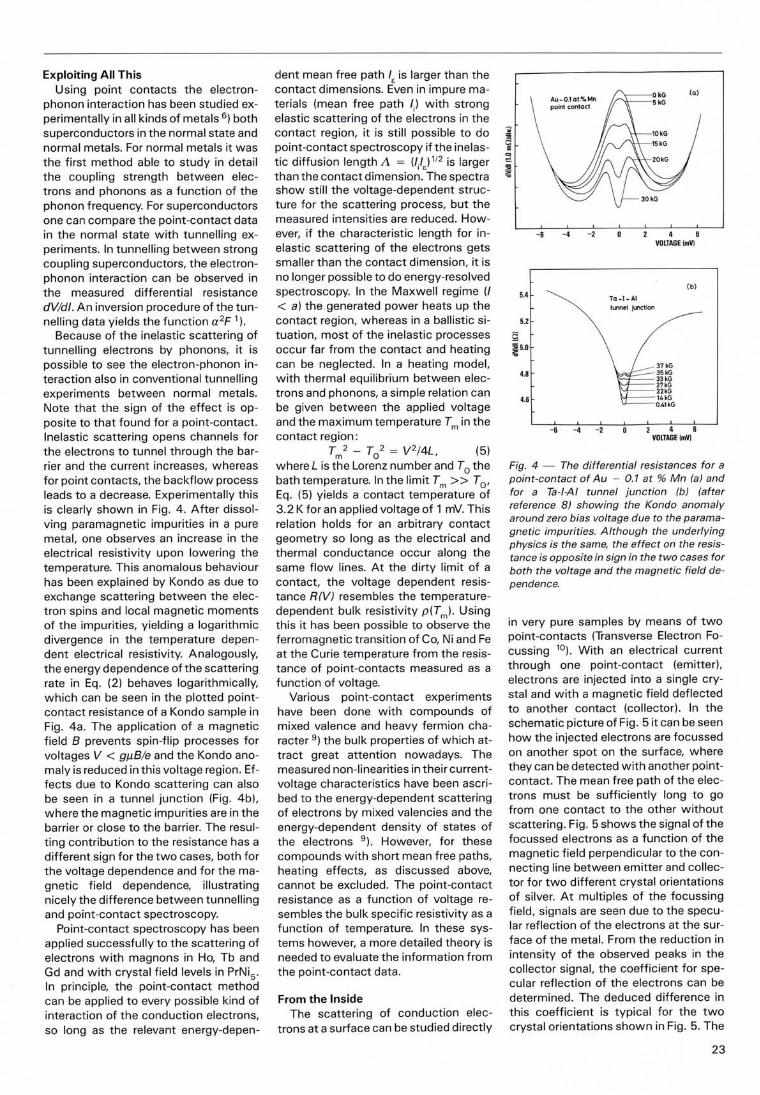
Because of the inelastic scattering of tunnelling electrons by phonons, it is possible to see the electron-phonon interaction also in conventional tunnelling experiments between normal metals. Note that the sign of the effect is opposite to that found for a point-contact. Inelastic scattering opens channels for the electrons to tunnel through the barrier and the current increases, whereas for point contacts, the backflow process leads to a decrease. Experimentally this is clearly shown in Fig. 4. After dissolving paramagnetic impurities in a pure metal, one observes an increase in the electrical resistivity upon lowering the temperature. This anomalous behaviour has been explained by Kondo as due to exchange scattering between the electron spins and local magnetic moments of the impurities, yielding a logarithmic divergence in the temperature dependent electrical resistivity. Analogously, the energy dependence of the scattering rate in Eq. (2) behaves logarithmically, which can be seen in the plotted point- contact resistance of a Kondo sample in Fig. 4a. The application of a magnetic field B prevents spin-flip processes for voltages V < gµB/e and the Kondo anomaly is reduced in this voltage region. Effects due to Kondo scattering can also be seen in a tunnel junction (Fig. 4b), where the magnetic impurities are in the barrier or close to the barrier. The resulting contribution to the resistance has a different sign for the two cases, both for the voltage dependence and for the magnetic field dependence, illustrating nicely the difference between tunnelling and point-contact spectroscopy.
Point-contact spectroscopy has been applied successfully to the scattering of electrons with magnons in Ho, Tb and Gd and with crystal field levels in PrNi5. In principle, the point-contact method can be applied to every possible kind of interaction of the conduction electrons, so long as the relevant energy-depen
dent mean free path Iε is larger than the contact dimensions. Even in impure materials (mean free path Ii) with strong elastic scattering of the electrons in the contact region, it is still possible to do point-contact spectroscopy if the inelastic diffusion length Λ = (IiIε)1/2 is larger than the contact dimension. The spectra show still the voltage-dependent structure for the scattering process, but the measured intensities are reduced. However, if the characteristic length for inelastic scattering of the electrons gets smaller than the contact dimension, it is no longer possible to do energy-resolved spectroscopy. In the Maxwell regime (I < a) the generated power heats up the contact region, whereas in a ballistic situation, most of the inelastic processes occur far from the contact and heating can be neglected. In a heating model, with thermal equilibrium between electrons and phonons, a simple relation can be given between the applied voltage and the maximum temperature Tm in the contact region :
Tm2 - TO2 = V2/4L, (5)where L is the Lorenz number and TO the bath temperature. In the limit Tm >> TO, Eq. (5) yields a contact temperature of 3.2 K for an applied voltage of 1 mV. This relation holds for an arbitrary contact geometry so long as the electrical and thermal conductance occur along the same flow lines. At the dirty limit of a contact, the voltage dependent resistance R(V) resembles the temperature- dependent bulk resistivity p(Tm). Using this it has been possible to observe the ferromagnetic transition of Co, Ni and Fe at the Curie temperature from the resistance of point-contacts measured as a function of voltage.
Various point-contact experiments have been done with compounds of mixed valence and heavy fermion character 9) the bulk properties of which attract great attention nowadays. The measured non-linearities in their current- voltage characteristics have been ascribed to the energy-dependent scattering of electrons by mixed valencies and the energy-dependent density of states of the electrons 9). However, for these compounds with short mean free paths, heating effects, as discussed above, cannot be excluded. The point-contact resistance as a function of voltage resembles the bulk specific resistivity as a function of temperature. In these systems however, a more detailed theory is needed to evaluate the information from the point-contact data.
From the InsideThe scattering of conduction elec
trons at a surface can be studied directly
Fig. 4 — The differential resistances for a point-contact of Au - 0.1 at % Mn la) and for a Ta-I-Al tunnel junction (b) (after reference 8) showing the Kondo anomaly around zero bias voltage due to the paramagnetic impurities. Although the underlying physics is the same, the effect on the resistance is opposite in sign in the two cases for both the voltage and the magnetic field dependence.
in very pure samples by means of two point-contacts (Transverse Electron Focussing 10). With an electrical current through one point-contact (emitter), electrons are injected into a single crystal and with a magnetic field deflected to another contact (collector). In the schematic picture of Fig. 5 it can be seen how the injected electrons are focussed on another spot on the surface, where they can be detected with another point- contact. The mean free path of the electrons must be sufficiently long to go from one contact to the other without scattering. Fig. 5 shows the signal of the focussed electrons as a function of the magnetic field perpendicular to the connecting line between emitter and collector for two different crystal orientations of silver. At multiples of the focussing field, signals are seen due to the specular reflection of the electrons at the surface of the metal. From the reduction in intensity of the observed peaks in the collector signal, the coefficient for specular reflection of the electrons can be determined. The deduced difference in this coefficient is typical for the two crystal orientations shown in Fig. 5. The
23

Fig. 5 — (Left) Collector voltage as a function of magnetic field B in the Transverse Electron Focussing experiment, shown in the inset. At the peaks are given the number of reflections of the detected electrons at the [001] surface (a) and the [011] surface (b). (Right) Representative surface profiles for the same surfaces measured with the STM. The flat regions in the [001] surface (a) explain the high reflectivity in the TEF experiment.
high reflection on these Ag crystal surfaces suggests a flatness on the scale of the de Broglie wavelength (only 0.5 nm). Note: the point-contact technique looks at the surface from the inside.
From the outside, the crystal surfaces, which were prepared by chemical etching, optically appear merely to be rather rough, whereas the surface topology as seen by the Scanning Tunnelling Microscope presents a striking difference 11 ). One surface shows a terracelike structure with flat regions (dimension = 100 nm) separated by steep steps, the other has a more hilly form (Fig. 5). This could explain the difference in the observed reflection coefficients with TEF.
In detailed experiments with Transverse Electron Focussing one can study the reflection of electrons at the crystal surface under different conditions (roughness, contamination) and, by varying the emitter voltage, as a function of the excitation energy. The reflection of an electron at the interface between a
normal metal and a superconductor 12) has even been directly observed. Upon entering the superconductor, an electron from the normal metal condenses in a Cooper pair by withdrawing an extra electron from the normal metal. In order to conserve mass, momentum and charge, a quasi-particle with opposite mass, group velocity and charge, i.e. a hole, has to return back into the normal metal. An experimental arrangement for demonstrating this so-called Andreev reflection is shown schematically in Fig. 6 where two point-contacts are formed on one side of a silver crystal and an evaporated Pb film on the opposite. The detected signal at the collector is given for both positive and negative fields. The orientation of the Ag crystal is such that for positive fields electrons are focussed via nearly spherical belly orbits (α0, α1) on the Fermi surface and for negative fields via rosette orbits (β0, β1, β2). The belly and rosette orbits enclose electronic states with respectively lower and higher energy. In a magnetic field, there
fore, the electrons rotate in opposite directions for the two types of orbit. The γ-peak in Fig. 6 is due to an Andreev reflection at the bottom of the crystal. With respect to the other peaks, the signal is opposite in sign because of the positive charge of the reflected quasiparticles.
Adding Up ToIn summary, by the ballistic injection
of electrons through a well conducting but small constriction, the electronic system can be studied within the metal. With a tunnelling experiment, interpretation starts with the tunnelling process itself, i.e. the small overlap of electronic states in the two parts of the junction. Although the physical models for these two cases are totally different, the results obtained show analogies.
Very obviously, there has been a burst of activity on all sorts of problems around the tunnelling experiments of thirty years ago, culminating in the Scanning Tunnelling Microscope. Yan- son's discovery of point-contact spectroscopy is another highlight in this development. But this is certainly only the tip of a beautiful and exciting iceberg. Powerful new theoretical and experimental techniques have emerged, leading to new insights into simple and exotic materials. There is no question that there is more to come 13).
REFERENCES1. E. Burstein and S. Lundqvist eds., Tunnelling Phenomena in Solids (Plenum Press, New York) 1969.2. Baratoff A., Europhys. News 17 (1986) 141.3. Clarke J. and Schön G., Europhys. News 17 (1986) 94.4. Yanson I.K., Zh. Eksp. Teor. Fiz. 66 (1974) 1035 [Sov. Phys. -JETP 39 (1974) 506).5. Jansen A.G.M., van Gelder A.P. and Wyder P., J. Phys. C 13 (1980) 6073.6. Yanson I.K., Fiz. Nizk. Temp. 9 (1983) 676 [Sov. J. Low Temp. Phys. 9 (1983) 343].7. Sharvin Yu.V., Zh. Eksp. Teor. Fiz. 48 (1965) 984 [Sov. Phys. - JETP 21 (1965) 655].8. Shen L.Y.L. and Rowell J.M., Phys. Rev. 165 (1968) 566.9. Bussian B., Frankowski I. and Wohlleben D., Phys. Rev. Lett. 49 (1982) 1026; Moser M., Wachter P., Franse J.J.M., Meisner G.P. and Walker E., Magn. Magn. Mat. 54-57 (1986) 373.10. Tsoi V.S. and Pis'ma Zh., Eksp. Teor. Fiz. 19 (1974) 114 [JETP Lett. 19 (1974) 70].11. Van Kempen H., Benistant P.A.M., van de Walle G.F.A. and Wyder P., Phys. Rev. B 133 (1986) 690.12. Benistant P.A.M., van Kempen H. and Wyder P, Phys. Rev. Lett. 51 (1983) 817.13. Wohlleben D., Paulus E., Voss G. and Freimuth A., Europhys. Lett. 3 (1987) 107.
Fig. 6 — Collector voltage as a function of the magnetic field B for an Ag crystal with an evaporated Pb film. The inset shows the trajectories of the quasi particles from emitter E to collector C upon Andreev reflection at the normal metal — superconductor interface illustrating that belly-electrons have - charge and + mass, rossette-electrons have - charge mass, and Andreev-reflected electrons have + charge and - mass.
24