Embed Size (px)
DESCRIPTION
semiconductors
Citation preview

1
Lecture 7: Electrostatics and IV Characteristics of P-N DiodeECE5590: Nanoscale Devices and circuits
Mostafizur [email protected]
• R-G, Drift, Diffusion• Continuity Equation• P-N Junction
Recap

3
Outline
• P-N Junctions• Drawing Band Diagram• Solution in Equilibrium• Non-Equilibrium Conditions (I-V)• Summary
ECE5590 Fall 2015 MR

ECE5590 Fall 2015 MR 4

ECE5590 Fall 2015 MR 5

ECE5590 Fall 2015 MR 6
P-N Junction Devices..

ECE5590 Fall 2015 MR 7
P and N doped Materials

ECE5590 Fall 2015 MR 8
Time < 0
P-type piece N-type piece
Time < 0: Pieces separated

At time = 0, slam the two pieces together

ECE 663
At time = 0, slam the two pieces together

Hole gradient
Jp, diffusion = -qDp dp/dx = current right, holes right
Electron gradient
Jn,diffusion = -qDn dn/dx = current right, electrons right
Gradients drive diffusion
left

E
E
Depletion Region

ECE5590 Fall 2015 MR 13
Depletion Approximation

ECE5590 Fall 2015 MR 14
Electrostatics
• Poisson’s Equation

ECE5590 Fall 2015 MR 15

ECE5590 Fall 2015 MR 16
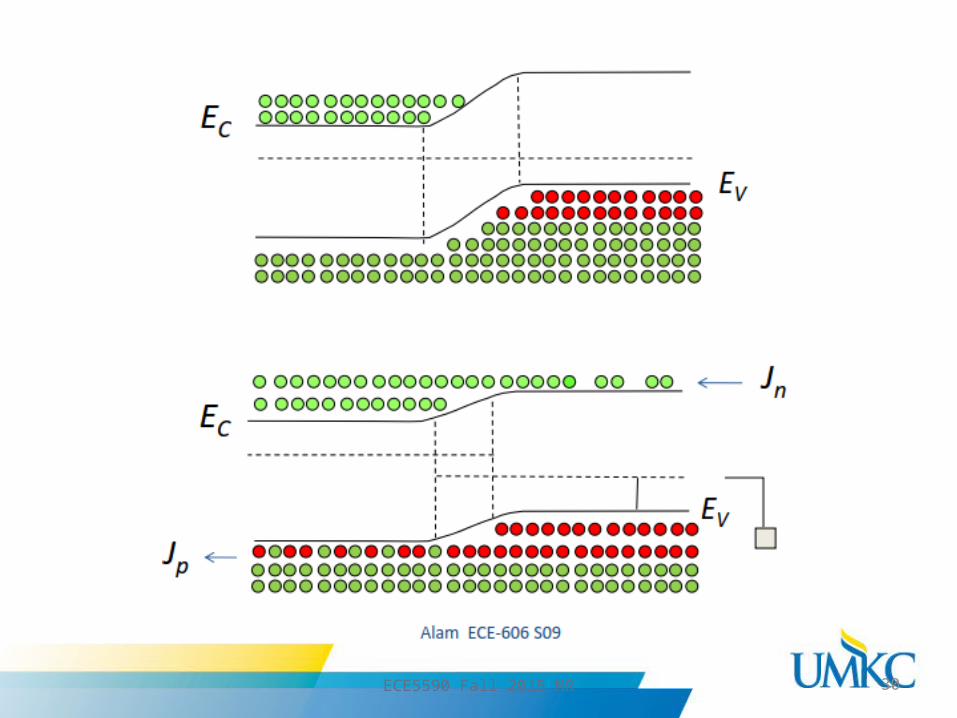
Drawing Band diagram
ECE5590 Fall 2015 MR 17
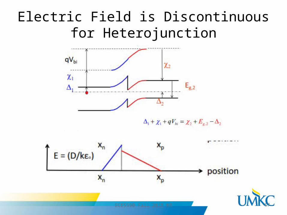
Electric Field is Discontinuous for Heterojunction

ECE5590 Fall 2015 MR 18
Homojunction

ECE5590 Fall 2015 MR 19
Built-in Potential (Vbi)

How wide is the depletion region?

ECE 663
Depletion Approximation-step junction
x

ECE5590 Fall 2015 MR 22
Solution for E

ECE5590 Fall 2015 MR 23
Solution for E

ECE5590 Fall 2015 MR 24
Solution for V

ECE5590 Fall 2015 MR 25
Depletion Width

ECE5590 Fall 2015 MR 26
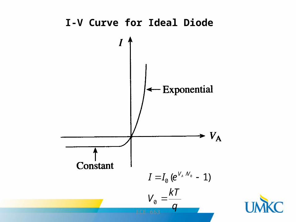
I-V Characteristics

ECE5590 Fall 2015 MR 27

ECE5590 Fall 2015 MR 28
Applying a Bias

ECE5590 Fall 2015 MR 29
Depletion Width
• Would current flow? Diffusion/Drift?
ECE5590 Fall 2015 MR 30

ECE5590 Fall 2015 MR 31
Effect of Bias
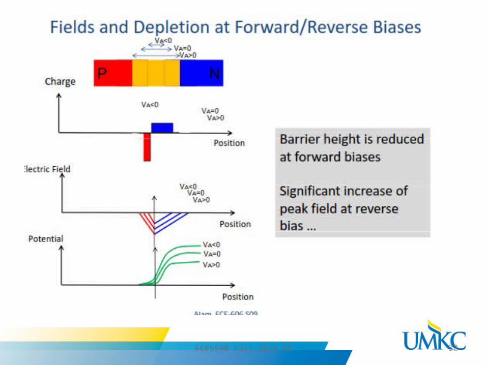
ECE5590 Fall 2015 MR 32
ECE 663
I-V Curve for Ideal Diode
qkT
V
eII VVA
0
/0 )1( 0
ECE 663
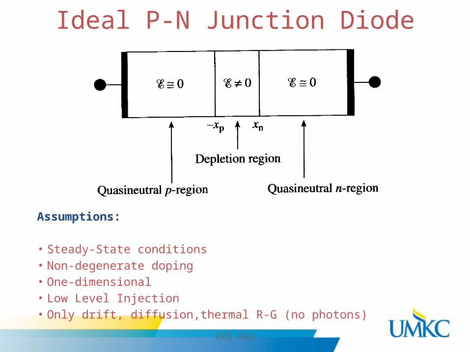
Ideal P-N Junction Diode
Assumptions:
• Steady-State conditions• Non-degenerate doping• One-dimensional• Low Level Injection• Only drift, diffusion,thermal R-G (no photons)

ECE5590 Fall 2015 MR 35

ECE5590 Fall 2015 MR 36
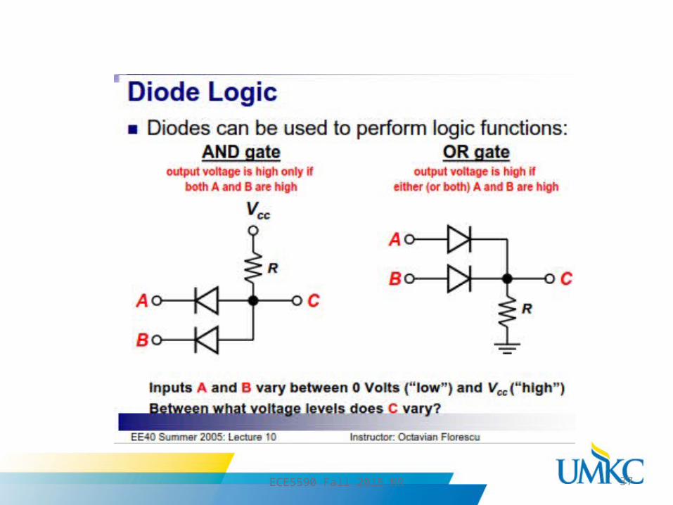
Applications
ECE5590 Fall 2015 MR 37

ECE5590 Fall 2015 MR 38
Solar Cells

ECE5590 Fall 2015 MR 39
Solar Cells
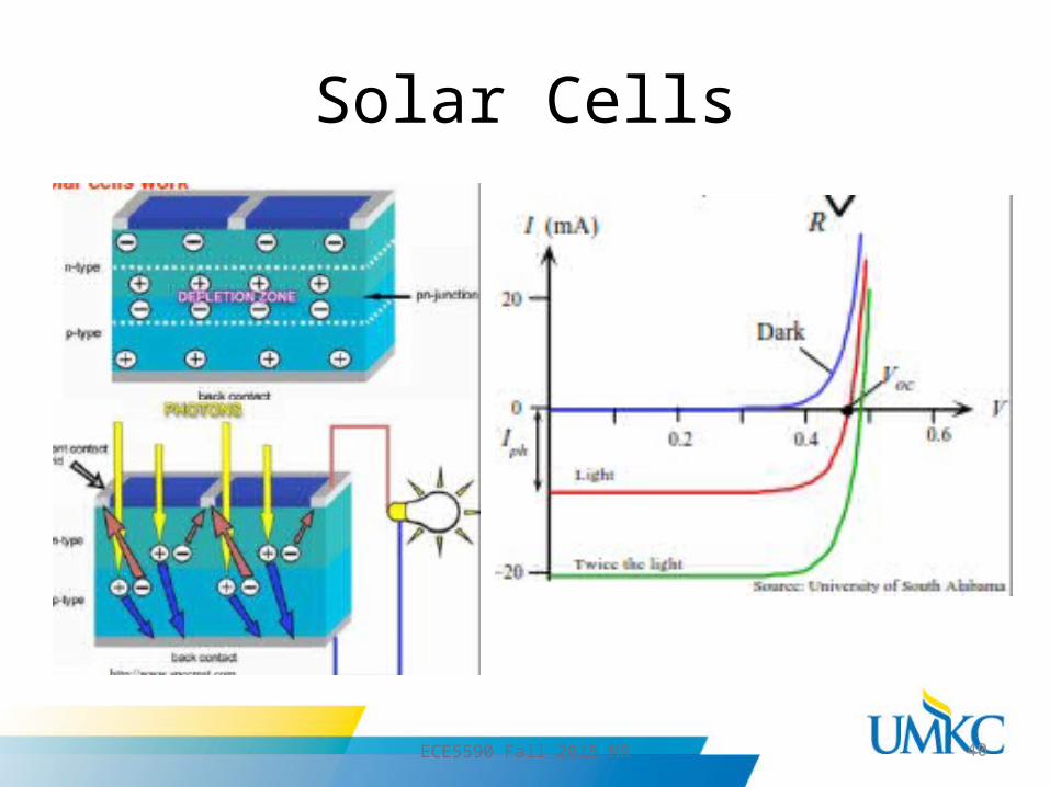
ECE5590 Fall 2015 MR 40
Solar Cells

ECE5590 Fall 2015 MR 41
Summary
• P-N diodes are simplest semiconductor devices
• Operation lies in fundamental of physics• Useful for various applications


![$$ 5 - . 1 ) $ · ... PN junction, Junction Theory, VI characteristics of PN junction diode, Ideal diode, Static and Dynamic Resistance [1][2], Diode current equation[2],Diode notations](https://img.pdfslide.us/doc/110x75/5ae6f8997f8b9a29048e3147/-5-1-pn-junction-junction-theory-vi-characteristics-of-pn-junction.jpg)