Embed Size (px)
Citation preview
Plug-In Hybrid Electric Vehicle Charger System
Senior Project Final Report
By: Matthew Daly, Peter Burrmann & Renee Kohl
Advisors: Dr. Woonki Na & Dr. Brian Huggins
May 9th 2012
2
Table of Contents Abstract ......................................................................................................................................................... 3
Introduction .................................................................................................................................................. 4
Project Description........................................................................................................................................ 4
Theory ....................................................................................................................................................... 5
High Power System ................................................................................................................................... 5
AC/DC Diode Rectifier ........................................................................................................................... 6
Bi-Directional Converter ....................................................................................................................... 6
Boost Converter and Power Factor Correction ..................................................................................... 7
Buck Converter ...................................................................................................................................... 8
Low Power/Interfacing System ................................................................................................................. 9
Current Transducer ................................................................................................................................. 11
Gate Driver .............................................................................................................................................. 11
Li-Ion Battery ............................................................................................................................................... 13
Internal Resistance .................................................................................................................................. 15
Software/Controller .................................................................................................................................... 16
Bi-directional Converter .......................................................................................................................... 21
Completed Work ......................................................................................................................................... 27
Future Work ................................................................................................................................................ 27
IMPLEMENTATION AND SIMULATION ........................................................................................................ 27
Experimental/Simulation Setup, Results and Discussion ........................................................................ 28
Power factor Correction...................................................................................................................... 28
Bi-Directional Converter (Buck and Boost) ......................................................................................... 29
Overall Schematic ............................................................................................................................... 33
Conclusion ................................................................................................................................................... 34
3
Abstract
A Plug-in Hybrid Electric Vehicle (PHEV) is not only a hybrid vehicle which utilizes a
battery to power the vehicle’s electric motor, but also its battery can be recharged when it is
plugged-in to a power source (typically 120V,rms) from the grid. PHEVs have much higher fuel
efficiency and lower operating cost than the conventional internal cobusition engine based
vehicle. These electric vehicles help keep the environment clean by reducing the amount of
toxins emitted from standard exhaust systems. The primary goal of this project was to design a
charging and discharging system for the PHVEs vehicles through the use of Digital Signal
Processor(DSP) based power electronics systems. In this report, the progress toward this goal is
addressed with using a 400W, 51.8V Li-Ion batteries and a Texas Instrument 32-bit fixed-point
DSP TMS320F2812.
4
Introduction Lately, the hybrid drivetrain technology has drawn attention of the both media and
automobile consumers because vehicles employing the hybrid technology can significantly
improve their fuel economy and produce less pollutants compared to conventional vehicles. For
further seeking a better hybrid electric vehicle(HEV) technology, the plug-in-hybrid electrical
vehicle(PHEV) emerges by incorporating this hybrid technology with adding the function of
plug-in-charging from the utility grid. For a PHEV, it needs a larger motor, more energy storages
such as batteries or ultracapacitors and less space for engine and gas tank comparing with the
normal hybrid vehicle.
Project Description The primary goal of this project is to design a system that will function as an electric
vehicle charger. A Digital Signal Processor (DSP) driven power electronics system shall be
designed such that the system can convert 120V, rms AC grid power to the required 51.8V,peak
DC value to charge an electric vehicle battery. This system will consist of a single phase diode
rectifier, boost converter, and bi-directional converter for discharging the battery into a variable
load or charging of the battery itself. In order to implement this system, a control algorithm is to
be developed using the TMS320F2812 DSP board. Values for all circuit elements need to be
calculated and specific devices and circuit elements need to be selected and purchased to meet
the system specifications.
5
Theory The design of an onboard battery charger is not as simple as connecting the battery
straight to the grid. The power charging the battery must be within certain specifications to
prevent damage to the battery and overall system. In terms of PHEVs, the high- energy battery
pack is to be charged with Power Factor Correction(PFC) from an AC outlet. The most common
topology for the PHEV battery charger is the two-stage approach with cascaded PFC AC-DC and
DC-DC converters. In the PFC stage, AC single phase is rectified and boosted with power factor
correction. The output of the boost converter is connected to the DC bus, and a bidirectional
converter for the battery charging or discharging is also connected to this DC bus.
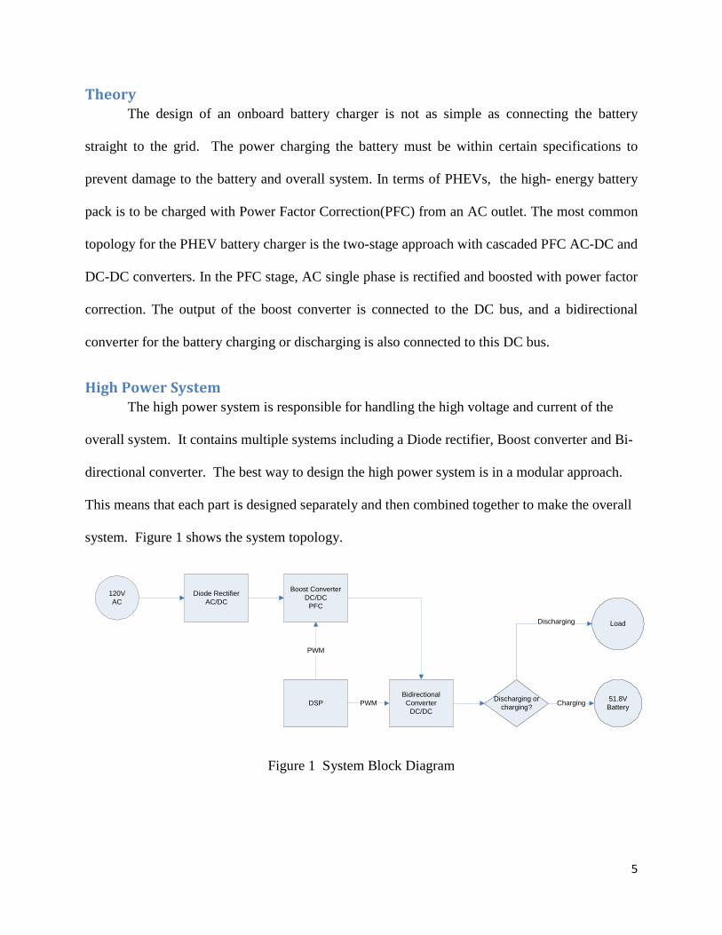
High Power System The high power system is responsible for handling the high voltage and current of the
overall system. It contains multiple systems including a Diode rectifier, Boost converter and Bi-
directional converter. The best way to design the high power system is in a modular approach.
This means that each part is designed separately and then combined together to make the overall
system. Figure 1 shows the system topology.
Figure 1 System Block Diagram
120VAC
Diode RectifierAC/DC
Boost ConverterDC/DC
PFC
Bidirectional Converter
DC/DC
51.8VBatteryDSP
PWM
PWM
Load
Discharging or charging? Charging
Discharging
6
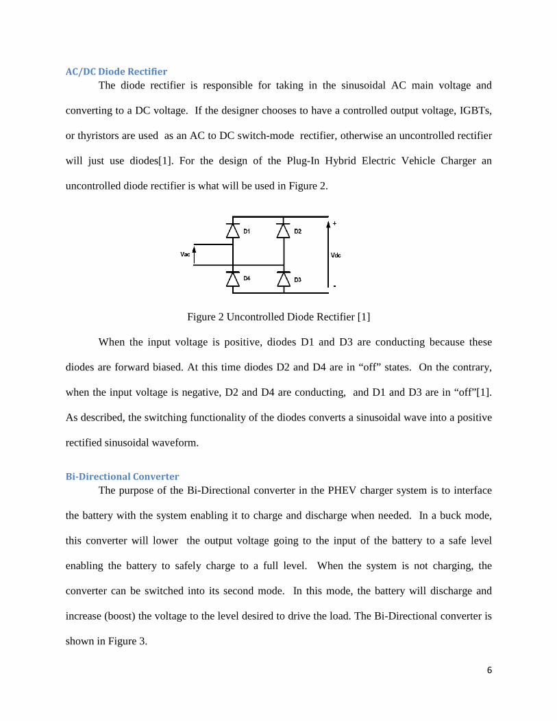
AC/DC Diode Rectifier The diode rectifier is responsible for taking in the sinusoidal AC main voltage and
converting to a DC voltage. If the designer chooses to have a controlled output voltage, IGBTs,
or thyristors are used as an AC to DC switch-mode rectifier, otherwise an uncontrolled rectifier
will just use diodes[1]. For the design of the Plug-In Hybrid Electric Vehicle Charger an
uncontrolled diode rectifier is what will be used in Figure 2.
Figure 2 Uncontrolled Diode Rectifier [1]
When the input voltage is positive, diodes D1 and D3 are conducting because these
diodes are forward biased. At this time diodes D2 and D4 are in “off” states. On the contrary,
when the input voltage is negative, D2 and D4 are conducting, and D1 and D3 are in “off”[1].
As described, the switching functionality of the diodes converts a sinusoidal wave into a positive
rectified sinusoidal waveform.
Bi-Directional Converter The purpose of the Bi-Directional converter in the PHEV charger system is to interface
the battery with the system enabling it to charge and discharge when needed. In a buck mode,
this converter will lower the output voltage going to the input of the battery to a safe level
enabling the battery to safely charge to a full level. When the system is not charging, the
converter can be switched into its second mode. In this mode, the battery will discharge and
increase (boost) the voltage to the level desired to drive the load. The Bi-Directional converter is
shown in Figure 3.
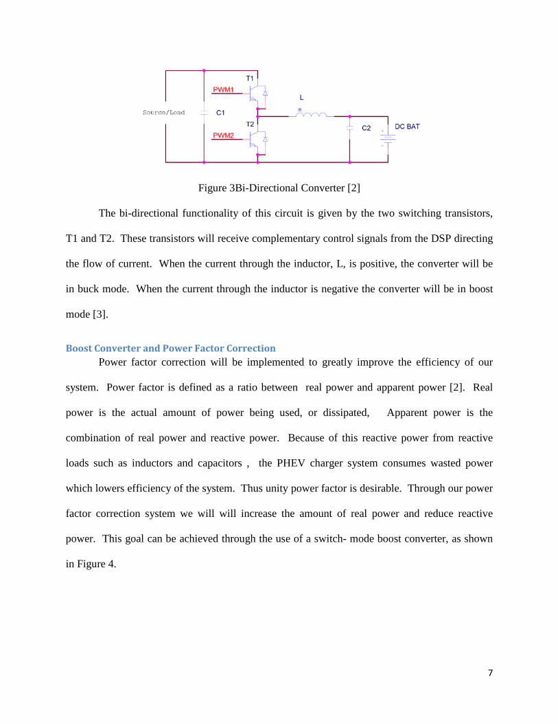
7
Figure 3Bi-Directional Converter [2]
The bi-directional functionality of this circuit is given by the two switching transistors,
T1 and T2. These transistors will receive complementary control signals from the DSP directing
the flow of current. When the current through the inductor, L, is positive, the converter will be
in buck mode. When the current through the inductor is negative the converter will be in boost
mode [3].
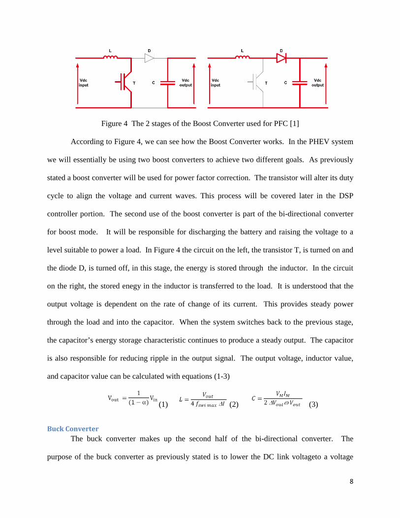
Boost Converter and Power Factor Correction Power factor correction will be implemented to greatly improve the efficiency of our
system. Power factor is defined as a ratio between real power and apparent power [2]. Real
power is the actual amount of power being used, or dissipated, Apparent power is the
combination of real power and reactive power. Because of this reactive power from reactive
loads such as inductors and capacitors , the PHEV charger system consumes wasted power
which lowers efficiency of the system. Thus unity power factor is desirable. Through our power
factor correction system we will will increase the amount of real power and reduce reactive
power. This goal can be achieved through the use of a switch- mode boost converter, as shown
in Figure 4.
8
Figure 4 The 2 stages of the Boost Converter used for PFC [1]
According to Figure 4, we can see how the Boost Converter works. In the PHEV system
we will essentially be using two boost converters to achieve two different goals. As previously
stated a boost converter will be used for power factor correction. The transistor will alter its duty
cycle to align the voltage and current waves. This process will be covered later in the DSP
controller portion. The second use of the boost converter is part of the bi-directional converter
for boost mode. It will be responsible for discharging the battery and raising the voltage to a
level suitable to power a load. In Figure 4 the circuit on the left, the transistor T, is turned on and
the diode D, is turned off, in this stage, the energy is stored through the inductor. In the circuit
on the right, the stored enegy in the inductor is transferred to the load. It is understood that the
output voltage is dependent on the rate of change of its current. This provides steady power
through the load and into the capacitor. When the system switches back to the previous stage,
the capacitor’s energy storage characteristic continues to produce a steady output. The capacitor
is also responsible for reducing ripple in the output signal. The output voltage, inductor value,
and capacitor value can be calculated with equations (1-3)
(1) (2) (3)
Buck Converter The buck converter makes up the second half of the bi-directional converter. The
purpose of the buck converter as previously stated is to lower the DC link voltageto a voltage
9
suitable to charge the DC battery. If too much voltage were to go into the battery it would be
destroyed.
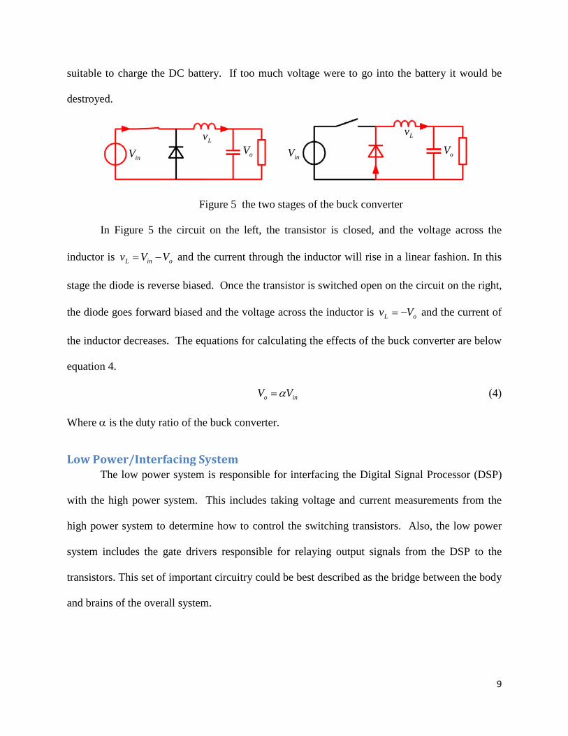
Figure 5 the two stages of the buck converter
In Figure 5 the circuit on the left, the transistor is closed, and the voltage across the
inductor is oinL VVv −= and the current through the inductor will rise in a linear fashion. In this
stage the diode is reverse biased. Once the transistor is switched open on the circuit on the right,
the diode goes forward biased and the voltage across the inductor is oL Vv −= and the current of
the inductor decreases. The equations for calculating the effects of the buck converter are below
equation 4.
ino VV α= (4)
Where α is the duty ratio of the buck converter.
Low Power/Interfacing System The low power system is responsible for interfacing the Digital Signal Processor (DSP)
with the high power system. This includes taking voltage and current measurements from the
high power system to determine how to control the switching transistors. Also, the low power
system includes the gate drivers responsible for relaying output signals from the DSP to the
transistors. This set of important circuitry could be best described as the bridge between the body
and brains of the overall system.
inV Lv
oV inV
Lv
oV
10
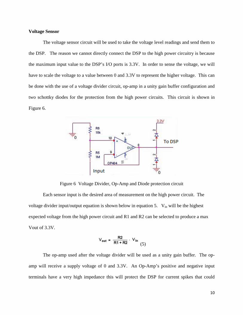
Voltage Sensor
The voltage sensor circuit will be used to take the voltage level readings and send them to
the DSP. The reason we cannot directly connect the DSP to the high power circuitry is because
the maximum input value to the DSP’s I/O ports is 3.3V. In order to sense the voltage, we will
have to scale the voltage to a value between 0 and 3.3V to represent the higher voltage. This can
be done with the use of a voltage divider circuit, op-amp in a unity gain buffer configuration and
two schottky diodes for the protection from the high power circuits. This circuit is shown in
Figure 6.
Figure 6 Voltage Divider, Op-Amp and Diode protection circuit
Each sensor input is the desired area of measurement on the high power circuit. The
voltage divider input/output equation is shown below in equation 5. Vin will be the highest
expected voltage from the high power circuit and R1 and R2 can be selected to produce a max
Vout of 3.3V.
(5)
The op-amp used after the voltage divider will be used as a unity gain buffer. The op-
amp will receive a supply voltage of 0 and 3.3V. An Op-Amp’s positive and negative input
terminals have a very high impedance this will protect the DSP for current spikes that could
11
destroy the DSP. The reason we use the Op-Amp in a unity gain buffer configuration is to utilize
the high impedance feature while keeping the voltage the same as the input. Lastly there are two
schottky diodes, one connected from the output to 3.3V and the other is connected from ground
to the output. In the case of a voltage that goes above 3.3V or below 0 volts into the negative
range the diodes will pull the voltage to 0 or 3.3V, protecting the delicate hardware of the DSP.
Current Transducer A current transducer will be used to detect current values in the high power circuit.
These values will be sent to the DSP to control the switching of the transistors in the high power
sub-systems. The current transducer uses the Hall Effect to represent the current value as a
voltage. The output voltage of our current transducers is 4V and unfortunately cannot be fed
directly into the DSP. In order to work around this we implemented the voltage sensor circuit
and adjusted the voltage divider to handle an input of 4 and output 0V to 3.3V.
Gate Driver The gate drivers are used as a medium between the pulse-width modulated output of the
DSP and the input to the switching transistors of the high power circuit. Gate drivers are needed
because the DSP’s PWM output does not supply a high enough voltage to physically switch the
transistor. The gate driver has its own power supply and simulates the DSP’s output at a higher
power level to effectively control the switching characteristic of the transistor. The IRFP460A
high power MOSFET used in this system requires a gate-to-source voltage of approximately 12V
to completely turn on. Since the DSP provides an output PWM of approximately 3.3V at low
current, the gate driver would need to provide extra power to the signal to fully turn on the
MOSFETs. For the MOSFETs involved in this system, the IR2110 gate driver was selected.
The IR2110 is operational for high voltage applications (up to 600V). Figure 7 shows a typical
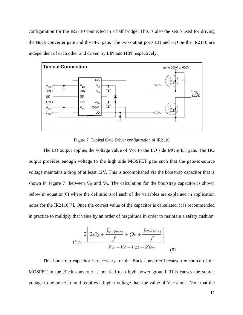
12
configuration for the IR2110 connected to a half bridge. This is also the setup used for driving
the Buck converter gate and the PFC gate. The two output ports LO and HO on the IR2110 are
independent of each other and driven by LIN and HIN respectively.
Figure 7 Typical Gate Driver configuration of IR2110
The LO output applies the voltage value of Vcc to the LO side MOSFET gate. The HO
output provides enough voltage to the high side MOSFET gate such that the gate-to-source
voltage maintains a drop of at least 12V. This is accomplished via the bootstrap capacitor that is
shown in Figure 7 between VB and VS. The calculation for the bootstrap capacitor is shown
below in equation(6) where the definitions of each of the variables are explained in application
notes for the IR2110[7]. Once the correct value of the capacitor is calculated, it is recommended
in practice to multiply that value by an order of magnitude in order to maintain a safety cushion.
(6)
This bootstrap capacitor is necessary for the Buck converter because the source of the
MOSFET in the Buck converter is not tied to a high power ground. This causes the source
voltage to be non-zero and requires a higher voltage than the value of Vcc alone. Note that the

13
frequency of operation plays an important role in what size this capacitor may be. As the high
side MOSFET turns off, current flows from Vcc through a diode into VB, and thereby charging
the bootstrap capacitor. Once the High side MOSFET needs to turn on, charge is pulled from the
capacitor and Vcc in order to produce the necessary increase in voltage for properly switching the
MOSFET.
Li-Ion Battery One of the primary goals of this project is to optimally charge a high power battery. The
battery selected for charging is a 14 Cell (58.8V) Lithium-Ion Polymer Battery with a total rated
capacity of 10[Ah] and can be seen in Figure 8.
Figure 8 58.8[V] Lithium Ion battery pack
In order to optimally charge a Li-Ion battery, an understanding of various charging methods and
charging stages of Li-Ion cells is necessary. A break-down of the charging stages can be seen in
Figure 9. Note that the plot applies to a single Lithium cell.
14
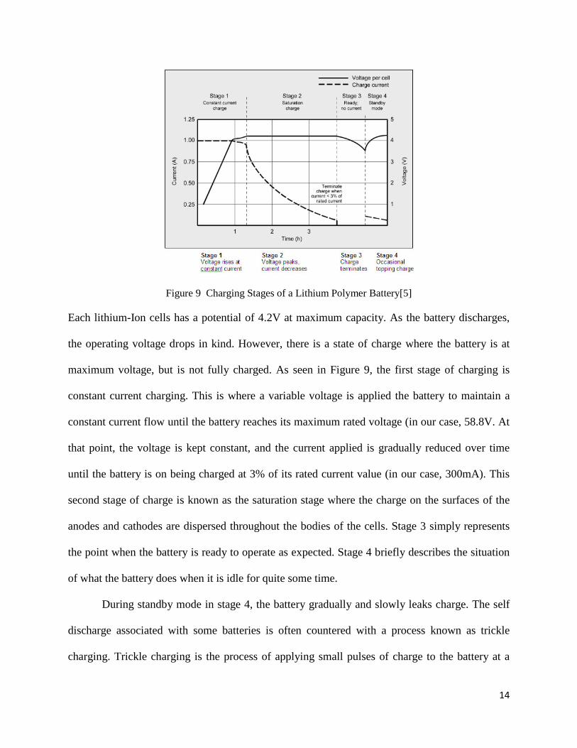
Figure 9 Charging Stages of a Lithium Polymer Battery[5]
Each lithium-Ion cells has a potential of 4.2V at maximum capacity. As the battery discharges,
the operating voltage drops in kind. However, there is a state of charge where the battery is at
maximum voltage, but is not fully charged. As seen in Figure 9, the first stage of charging is
constant current charging. This is where a variable voltage is applied the battery to maintain a
constant current flow until the battery reaches its maximum rated voltage (in our case, 58.8V. At
that point, the voltage is kept constant, and the current applied is gradually reduced over time
until the battery is on being charged at 3% of its rated current value (in our case, 300mA). This
second stage of charge is known as the saturation stage where the charge on the surfaces of the
anodes and cathodes are dispersed throughout the bodies of the cells. Stage 3 simply represents
the point when the battery is ready to operate as expected. Stage 4 briefly describes the situation
of what the battery does when it is idle for quite some time.
During standby mode in stage 4, the battery gradually and slowly leaks charge. The self
discharge associated with some batteries is often countered with a process known as trickle
charging. Trickle charging is the process of applying small pulses of charge to the battery at a
15
rate equal to the self discharge of the battery. While this sounds good on paper, this is a poor
plan for Li-Ion batteries. Maintaining maximum state of charge on a Li-Ion battery puts a large
amount of stress on the cells, and shortens the overall lifespan of the battery. Maintaining
maximum charge or even potential over-charge causes metallic lithium plating on the cell nodes.
The plating causes poor power transfer during charging and discharging and ends up dissipating
large amounts of energy into heat.
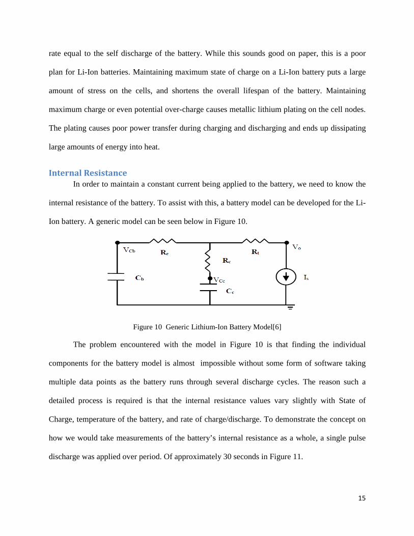
Internal Resistance In order to maintain a constant current being applied to the battery, we need to know the
internal resistance of the battery. To assist with this, a battery model can be developed for the Li-
Ion battery. A generic model can be seen below in Figure 10.
Figure 10 Generic Lithium-Ion Battery Model[6]
The problem encountered with the model in Figure 10 is that finding the individual
components for the battery model is almost impossible without some form of software taking
multiple data points as the battery runs through several discharge cycles. The reason such a
detailed process is required is that the internal resistance values vary slightly with State of
Charge, temperature of the battery, and rate of charge/discharge. To demonstrate the concept on
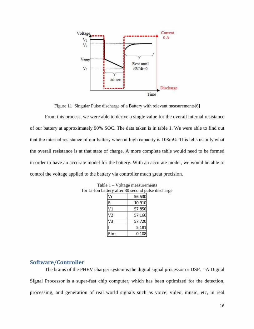
how we would take measurements of the battery’s internal resistance as a whole, a single pulse
discharge was applied over period. Of approximately 30 seconds in Figure 11.
16
Figure 11 Singular Pulse discharge of a Battery with relevant measurements[6]
From this process, we were able to derive a single value for the overall internal resistance
of our battery at approximately 90% SOC. The data taken is in table 1. We were able to find out
that the internal resistance of our battery when at high capacity is 108mΩ. This tells us only what
the overall resistance is at that state of charge. A more complete table would need to be formed
in order to have an accurate model for the battery. With an accurate model, we would be able to
control the voltage applied to the battery via controller much great precision.
Table 1 – Voltage measurements for Li-Ion battery after 30 second pulse discharge
Software/Controller The brains of the PHEV charger system is the digital signal processor or DSP. “A Digital
Signal Processor is a super-fast chip computer, which has been optimized for the detection,
processing, and generation of real world signals such as voice, video, music, etc, in real
Vr 56.530R 10.910V1 57.850V2 57.160V3 57.720I 5.181Rint 0.108
17
time.”[5]. This fast, high precision processor is ideal for controlling the overall converter system.
The DSP is programmed with C code. C code can be written or generated with a block diagram
model via Matlab Simulink toolboxes. As previously noted, the DSP can generate a pulse width
modulated signal which is fed to the gate drivers powering the switching transistors. Pulse width
modulation, or PWM, is generally a square wave signal with a constant frequency; the duty cycle
is then adjusted [4]. This adjustment of the duty cycle is what determines the on and off time of
the switching transistors. For the PHEV charger system, dead-band will have to be incorporated
into the PWM signal to prevent switching crossover. “Dead-band separates the transition edges
of two signals: output and complemented output, by a time interval.”[4] The purpose of dead-
band is to protect the sensitive hardware on the high power side. If two complementary
transistors are on at the same time, damage and instability of the power circuits will occur.
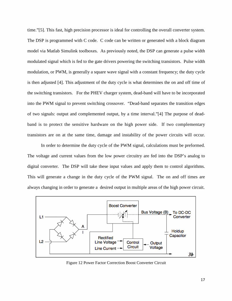
In order to determine the duty cycle of the PWM signal, calculations must be preformed.
The voltage and current values from the low power circuitry are fed into the DSP’s analog to
digital converter. The DSP will take these input values and apply them to control algorithms.
This will generate a change in the duty cycle of the PWM signal. The on and off times are
always changing in order to generate a desired output in multiple areas of the high power circuit.
Figure 12 Power Factor Correction Boost Converter Circuit
18
As seen in Figure 12, the PFC circuit is controlled by the DSP. The DSP reads in the rectified sine wave
input, the current through the inductor, and the output voltage. As mentioned earlier we are using this
active power factor correction method in attempt to achieve a unity power factor. The way this boost
converter circuit accomplishes that is by comparing the output voltage to a constant reference. This
reference value is the target output voltage that we choose. The error then passes through a PI controller
and then multiplied by the rectified sine wave to create a reference current. From there the current is
compared to the reference that was created and that error passes through a second PI controller. The
output is then the duty cycle that is sent to the MOSFET.
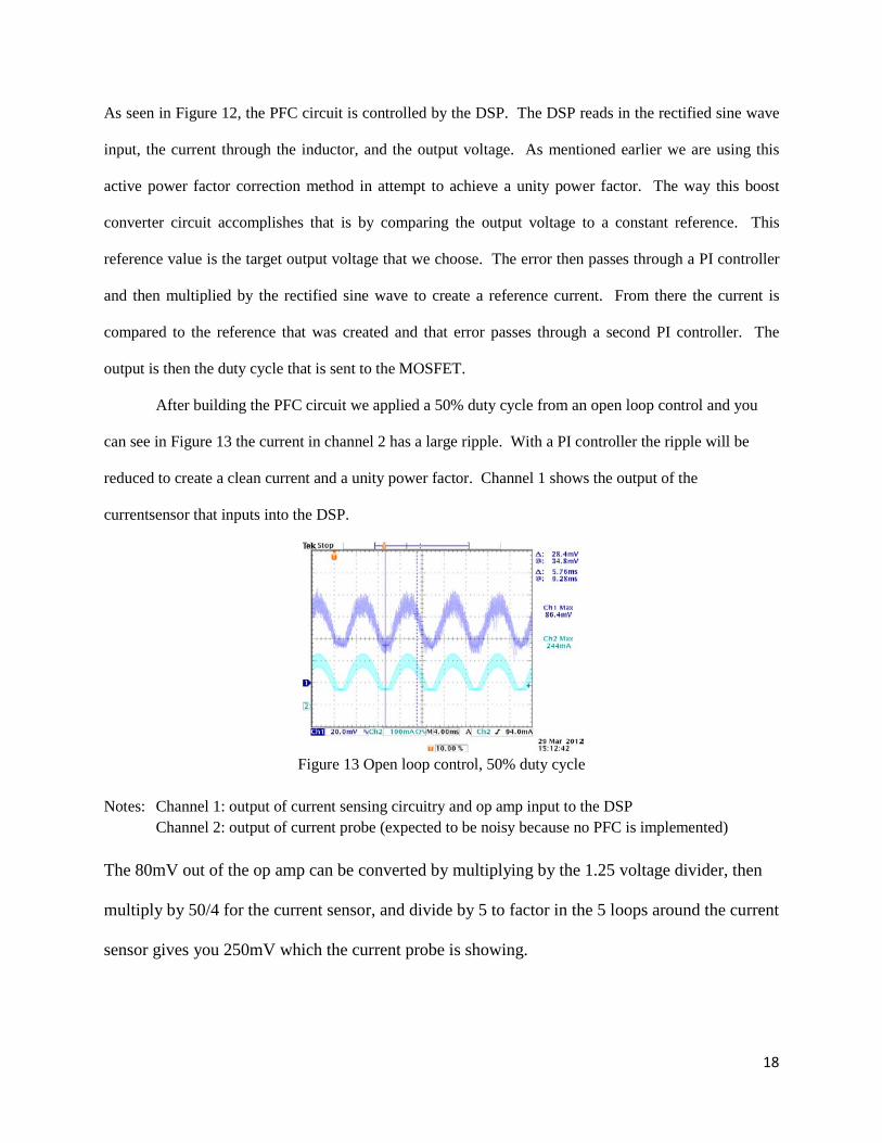
After building the PFC circuit we applied a 50% duty cycle from an open loop control and you
can see in Figure 13 the current in channel 2 has a large ripple. With a PI controller the ripple will be
reduced to create a clean current and a unity power factor. Channel 1 shows the output of the
currentsensor that inputs into the DSP.
Figure 13 Open loop control, 50% duty cycle
Notes: Channel 1: output of current sensing circuitry and op amp input to the DSP Channel 2: output of current probe (expected to be noisy because no PFC is implemented) The 80mV out of the op amp can be converted by multiplying by the 1.25 voltage divider, then
multiply by 50/4 for the current sensor, and divide by 5 to factor in the 5 loops around the current
sensor gives you 250mV which the current probe is showing.

19
To test the hysteresis control of the current we applied the control you see in Figure 14. We
simulated a current reference using a sine wave generator and an absolute value in Simulink.
After the actual current is read in through the ADC converter it is compared to the reference
value and if the reference is greater the pwm is high and vice versa. The current that previously
looked like channel 2 in (a) of Figure 13 was smoothed out to the current that appears on channel
2 in Figure 15.
Figure 14 Simulink hysteresis control
Because the current being measured by the DSP is a rectified sign wave with an amplitude of
approximately 80mV we simulated this in Simulink as the reference current to match.
20
(a) (b)
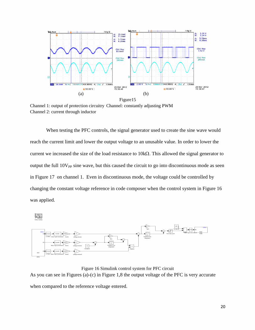
Figure15 Channel 1: output of protection circuitry Channel: constantly adjusting PWM Channel 2: current through inductor When testing the PFC controls, the signal generator used to create the sine wave would
reach the current limit and lower the output voltage to an unusable value. In order to lower the
current we increased the size of the load resistance to 10kΩ. This allowed the signal generator to
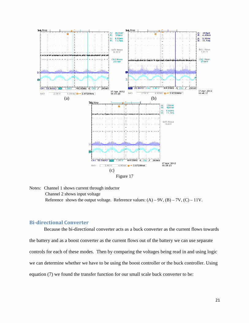
output the full 10VPP sine wave, but this caused the circuit to go into discontinuous mode as seen
in Figure 17 on channel 1. Even in discontinuous mode, the voltage could be controlled by
changing the constant voltage reference in code composer when the control system in Figure 16
was applied.
Figure 16 Simulink control system for PFC circuit
As you can see in Figures (a)-(c) in Figure 1,8 the output voltage of the PFC is very accurate
when compared to the reference voltage entered.
2
voltage divider3
6.7
voltage divider1
-K-
voltage divider
limit duty cycleinverter
In1Out1
iir fi l ter2
In1Out1
iir fi l ter1
Product
C281x
PWM
W1
PWM
-K-
Kp2
-K-
Kp1
.00073
Gain4
.00073
Gain2
.00073
Gain1
F2812 eZdsp1
K Ts
z-1Discrete-Time
Integrator2
K Ts
z-1Discrete-Time
Integrator1
double
Data Type Conversion3
uint16
Data Type Conversion2
double
Data Type Conversion1
double
Data Type Conversion
100
Constant2
15
Constant1
C281x
ADC
A4
A3
A5
ADC1
21
(a) (b)
(c)
Figure 17
Notes: Channel 1 shows current through inductor Channel 2 shows input voltage Reference shows the output voltage. Reference values: (A) – 9V, (B) – 7V, (C) – 11V.
Bi-directional Converter Because the bi-directional converter acts as a buck converter as the current flows towards
the battery and as a boost converter as the current flows out of the battery we can use separate
controls for each of these modes. Then by comparing the voltages being read in and using logic
we can determine whether we have to be using the boost controller or the buck controller. Using
equation (7) we found the transfer function for our small scale buck converter to be:

22
7
7
1002.27.3096.60601004.4
×+⋅+⋅+×
SSS
(7)
Using the Matlab code in Appendix A, we generated bode plots for the magnitude and phase of
the power stage of the buck converter as seen in Figure 18.
Figure 18 Phase and Magnitude plots for power stage Phase and Magnitude plots for power stage
From Figure 18 we can choose a crossover frequency, cf . As LC
fc π21
> we chose cf
=500Hz. Therefore, dBsGcfps 12.15|)(| = or 5.7, and °−=∠ 150)(
cfps sG .
The transfer function of our PI control block is:
sksk
sG ipc
+=)(
(8)
So the magnitude can be found by
22|)(|
+=ω
ipfc
kksGc
(9)

23
and phase
−=∠ −
p
i
fc k
k
sGc
ω1tan)(
(10)
In order to find the magnitude of the controller at our crossover frequency we use:
fbfpsfpwmfc ksGsGsGccc⋅⋅⋅= |)(||)(||)(|1 (11)
or
17.5263.|)(|1 ⋅⋅⋅=cfc sG
667.|)(| =cfc sG
We set the phase margin to be:
°= 60pmφ
We can then calculate the phase boost.
cfpspmboost sG )(90 ∠−+°−= φφ (12)
°−°+°−= 1506090boostφ
°−= 120boostφ
Once we have our phase boost we can calculate the phase of our controller at the crossover
frequency
(13)
°−=∠ 210)(cfc sG
so using the earlier equations for the magnitude and phase of the controller you can find our
gains to be:
24
1.806=ik and 444.=pk
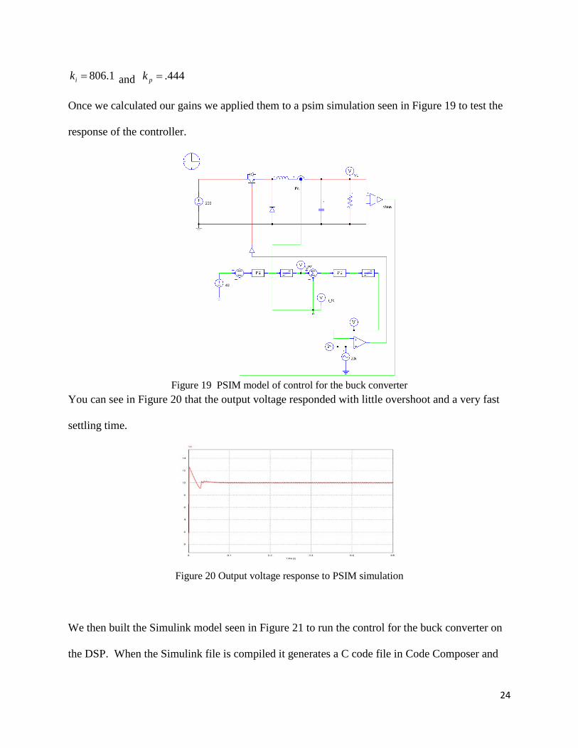
Once we calculated our gains we applied them to a psim simulation seen in Figure 19 to test the
response of the controller.
Figure 19 PSIM model of control for the buck converter
You can see in Figure 20 that the output voltage responded with little overshoot and a very fast
settling time.
Figure 20 Output voltage response to PSIM simulation
We then built the Simulink model seen in Figure 21 to run the control for the buck converter on
the DSP. When the Simulink file is compiled it generates a C code file in Code Composer and
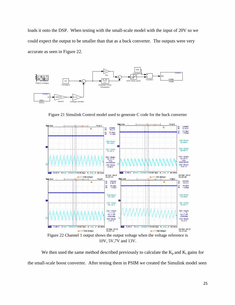
25
loads it onto the DSP. When testing with the small-scale model with the input of 20V so we
could expect the output to be smaller than that as a buck converter. The outputs were very
accurate as seen in Figure 22.
Figure 21 Simulink Control model used to generate C code for the buck converter
Figure 22 Channel 1 output shows the output voltage when the voltage reference is
10V, 5V,7V and 13V. We then used the same method described previously to calculate the Kp and Ki gains for
the small-scale boost converter. After testing them in PSIM we created the Simulink model seen
6.12
voltage divider
limit duty cycleinverter
C281x
PWM
W1
PWM
0.1
Kp
.00073
Gain4
F2812 eZdsp1
K Ts
z-1Discrete-Time
Integrator
100
Constant2
10
Constant
C281x
ADC
A
ADC1

26
in Figure 23. This again was compiled into Code Composer to generate C code for the DSP to
run.
Figure 23 Boost Converter control system in Simulink
With a 5V input into our system we can expect the output to be larger than that. As seen
below in Figure 24, the output voltages matched the constant reference value accurately.
6.12
voltage divider
limit duty cycleinverter
C281x
PWM
W1
PWM
0.1
Kp
.00073
Gain4
F2812 eZdsp1
K Ts
z-1Discrete-Time
Integrator
100
Constant2
10
Constant
C281x
ADC
A
ADC1

27
Figure 24 Results from closed loop boost converter. Channel 1 shows output voltage.
Completed Work Over the course of a year our team has successfully designed a full-scale system to
charge and discharge a battery from wall power. We constructed small-scale circuitry to design
the control systems. And from there constructed a full-scale buck converter and boost converter
that successfully implemented our control system on.
Future Work There is much work that can be done for any interested groups in the future who wish to
follow-up with this project. A future group could use the system to charge the battery. First the
team would need to acquire detailed parameters for battery. The team could also implement the
second stage of the system that discharges the battery through an inverter to run an AC induction
motor. With this motor would come the possibility of a regenerative braking system. In order to
optimally store the energy created by the regenerative braking, ultra-capacitors could be utilized
for quick charging capabilities.
IMPLEMENTATION AND SIMULATION Prior to this year, no Bradley Electrical Engineers have worked on this design. Under the
advisory of Dr. Na, we have started this project from the ground up. The information provided

28
ahead is a way to inform the reader about Power Electronic circuits used and how they are used
on a practical level given specific design specifications through simulation and lab results.
Experimental/Simulation Setup, Results and Discussion Based off of our calculations, we came up with capacitor values of 1500uF and inductor
values of 500uH. These values will work for both the power factor correction boost converter as
well as the bi-directional converter.
Power factor Correction Below is the simulation design of our Power Factor Correction circuit.
Figure 25 PSIM schematic of the power factor correction circuit (top half) and control system to be
implemented on the DSP (bottom half)
Something to note is that the voltage input in the simulation is 170Vac-peak but a wall
input is 120Vrms, both values are equal in some sense the 170V is a peak value while the 120V
outlet is rms value . We chose to use the 170V to be aware of the max possible input into our

29
circuit to get the best simulation results to develop a safe circuit. After running the PSIM
simulation, we acquired our desired results with the component values selected as well as a fine
tuned control system. For the Power Factor Correction circuitry in Figure 25, we wanted to
improve the power factor thus improving the efficiency as well as generating a DC output around
200Vdc.
Figure 26 Simulated Output generated from the PFC boost converter and Diode Rectifier circuit.
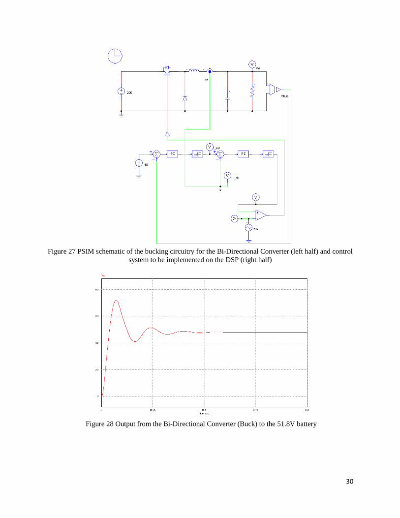
Bi-Directional Converter (Buck and Boost) We chose to simulate this in two parts, the boosting stage and the bucking stage. In the
final design this will only be one circuit. We designed the circuit to use a 51.8V Battery in our
system. As a result we will need to lower the 200V output from the Power Factor Conversion
Boost Converter to a safe 51.8V in order to charge the battery. The simulation results are shown
in Figure 28.
30
Figure 27 PSIM schematic of the bucking circuitry for the Bi-Directional Converter (left half) and control
system to be implemented on the DSP (right half)
Figure 28 Output from the Bi-Directional Converter (Buck) to the 51.8V battery
31
The above graph is the voltage output from the buck stage of the Bi-Directional Converter. The
Voltage reaches a steady state at 51.8V, which is our desired output to charge the battery. There
is a good amount of initial overshoot for the first 0.05 seconds. This could be reduced by further
tuning of the Proportional Integral control on the DSP.
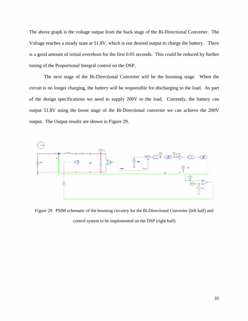
The next stage of the Bi-Directional Converter will be the boosting stage. When the
circuit is no longer charging, the battery will be responsible for discharging to the load. As part
of the design specifications we need to supply 200V to the load. Currently, the battery can
output 51.8V using the boost stage of the Bi-Directional converter we can achieve the 200V
output. The Output results are shown in Figure 29.
Figure 29 PSIM schematic of the boosting circuitry for the Bi-Directional Converter (left half) and
control system to be implemented on the DSP (right half)

32
Figure 30 Output from the Bi-Directional Converter (Boost) to the 200V load
Figure 30 is the voltage output from the boost stage of the Bi-Directional Converter. The
Voltage reaches a steady state at 200V. Like the buck converter, there is also some overshoot for
the first 0.2 seconds. This too can be reduced by further fine tuning the PI controller via the
DSP.
33
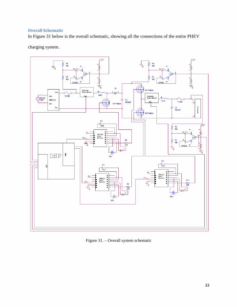
Overall Schematic In Figure 31 below is the overall schematic, showing all the connections of the entire PHEV
charging system.
Figure 31. – Overall system schematic

34
Conclusion The importance of hybrid and electric vehicles in growing in today’s society, due to the
need to reduce our dependency on foreign oil. Developing systems like the PHEV charger to
implement in vehicles is a huge step in that direction. Further research and development in the
field of technology will lead to a greener future.

35
References
[1] G. Mathieu, "Design of an on-board charger for plug-in hybrid electrical vehicle (PHEV)," Master Thesis, Chalmers University of Technology, Göteborg, Sweden, 2009. apply the theory provided, run simulations and design a control system. The amount of detail in this thesis helps clarify some of the difficult hurtles of the overall project.
[2] N. Mohan, First Course on Power Electronics. Minneapolis: MNPERE, 2009. [3] Y. Lee. A. Khaligh. and A. Emandi. (2009). Advanced integrated bidirectional AC/DC
and DC/DC converter for plug-in hybrid electric vehicles. IEEE Transactions on Vehicular Technology. [Online]. 58 (8), pp. 3970-3980. Available: http://ieeexplore.ieee.org.ezproxy .bradley.edu/stamp/stamp.jsp?tp=&arnumber=5170004
[4] B. Bagci, "Programming and use of TMS320F28I2 DSP to control and regulate power
electronic converters," Master Thesis, Fachochschule Koln University of Applied Sciences, Cologne, Germany, 2003.
[5] http://batteryuniversity.com/learn/article/charging_lithium_ion_batteries [6] http://www.nrel.gov/docs/fy01osti/28716.pdf [7] http://www.irf.com/technical-info/appnotes/an-978.pdf

36
Sources Consulted
D. M. Bellur and M. K. Kazimierczuk. (2007). DC-DC converters for electric vehicle applications. Electrical Insulation Conference and Electrical Manufacturing Expo. [Online]. pp. 286-293. Available: http://ieeexplore.ieee.org.ezproxy.bradley.edu/stamp/stamp.jsp?tp=&arn umber=4562633 L. Zhou, "Evaluation and DSP based implementation of PWM approaches for single-phased DC-AC converters," Master Thesis, Florida State University, Tallahassee, Florida, United States 2005. L. Zhu. (2004). A novel soft-commutating isolated boost full-bridge ZVS-PWM DC-DC converter for bidirectional high power applications. Power Electronics Specialists Conference. [Online]. 3, pp. 2141-2146. Available: http://ieeexplore.ieee.org.ezproxy .bradley.edu/stamp/stamp.jsp?tp=&arnumber=1355450 M. Hedlund, "Design and construction of a bidirectional DCDC converter for an EV application," Master Thesis, Uppsala University, Uppsala, Sweden, 2010. M. Marchesoni. (2007). New DC–DC converter for energy storage system interfacing in fuel cell hybrid electric vehicles. IEEE Transactions on Power Electronics. [Online]. 22 (1), pp. 301-308. Available: http://ieeexplore.ieee.org.ezproxy.bradley.edu/stamp/stamp.jsp?tp=& arnumber=4052425 Y. Tian, "Analysis, simulation and DSP based implementation of asymmetric three-level single-phase inverter in solar power system," Master Thesis, Florida State University, Tallahassee, Florida, United States, 2007.

37
Appendix A clear all close all num = [29971 4.3e8]; den = [1 1.3587e3 1.4347e7]; % voltage mode control Fig-4-18 figure(1) %f = linspace(30,30e3,500); % generate frequency points to be evaluated f = logspace(1,4,500); % generate frequency points in log scale w = 2*pi*f; % 'freqs' needs frequency in radians/sec H = freqs(num, den, w) % to obtain frequency responses: amplitude and phase amp = abs(H); % amp in linear scale phase = angle(H)*180/pi; magdB = 20*log10(amp); % magdB is the amplitude frequency response in decibel. figure(1), subplot(211), semilogx(f, magdB(1,:)), title('amplitude response in dB'),grid subplot(212),semilogx(f, phase(1,:)), title('phase response in degree') grid, xlabel('frequency in Hz'),ylabel('degree')

38
Appendix B
Materials/Parts List
• IRFP460A N-Type Power MOSFET o SK 145 Heat Sink
• IR2110 - 1PBF MOSFET Driver • NTE5328 – Bridge Rectifier • VS-HFA50PA60CPBF Power Diode • L08P050D15 Current Transducer • OP484FPZ Op-Amp • NXP - 74HC04N Hex Inverter • Aluminum Electrolytic Capacitor 1500uF, 400V • Inductor 500uH, 35A • Resistors & Power Resistors (Assorted Values) • 51.8V Li-ion Battery • Oscilloscope • DC Power Supply Unit • Signal Generator • DSP
o TMS320F2812 DSP o Code Composer Studio 3 o Mathworks Matlab & Simulink
• Psim Software