Embed Size (px)
Citation preview
DS90UB925Q
5 - 85 MHz 24-bit Color FPD-Link III Serializer with Bidirectional ControlChannel
General DescriptionThe DS90UB925Q serializer, in conjunction with theDS90UB926Q deserializer, provides a complete digital inter-face for concurrent transmission of high-speed video, audio,and control data for automotive display and image sensingapplications.
The chipset is ideally suited for automotive video-display sys-tems with HD formats and automotive vision systems withmegapixel resolutions. The DS90UB925Q incorporates anembedded bidirectional control channel and low latency GPIOcontrols. This chipset translates a parallel interface into a sin-gle pair high-speed serialized interface. The serial busscheme, FPD-Link III, supports full duplex of high-speed videodata transmission and bidirectional control communicationover a single differential link. Consolidation of video data andcontrol over a single differential pair reduces the interconnectsize and weight, while also eliminating skew issues and sim-plifying system design.
The DS90UB925Q serializer embeds the clock, DC scram-bles & balances the data payload, and level shifts the signalsto high-speed low voltage differential signaling. Up to 24 databits are serialized along the video control signals.
Serial transmission is optimized by a user selectable de-em-phasis. EMI is minimized by the use of low voltage differentialsignaling, data scrambling and randomization and spreadspectrum clocking compatibility.
Features Bidirectional control interface channel interface with I2C
compatible serial control bus
Supports high definition (720p) digital video format
RGB888 + VS, HS, DE and I2S audio supported
Supports two 10–bit camera video streams
5 – 85MHz PCLK supported
Single 3.3V Operation with 1.8V or 3.3V compatibleLVCMOS I/O interface
AC-coupled STP Interconnect up to 10 meters
Parallel LVCMOS video inputs
DC-balanced & scrambled Data w/ Embedded Clock
Supports repeater application
Internal pattern generation
Low power modes minimize power dissipation
Automotive grade product: AEC-Q100 Grade 2 qualified
>8kV HBM and ISO 10605 ESD rating
Backward compatible to FPD-Link II
Applications Automotive Display for Navigation
Rear Seat Entertainment Systems
Automotive Driver Assistance
Automotive Megapixel Camera Systems
Typical Display Applications Diagram
30143327
TRI-STATE® is a registered trademark of National Semiconductor Corporation.
PRODUCTION DATA information is current as ofpublication date. Products conform to specifications perthe terms of the Texas Instruments standard warranty.Production processing does not necessarily includetesting of all parameters.
301433 SNLS407A Copyright © 1999-2012, Texas Instruments Incorporated
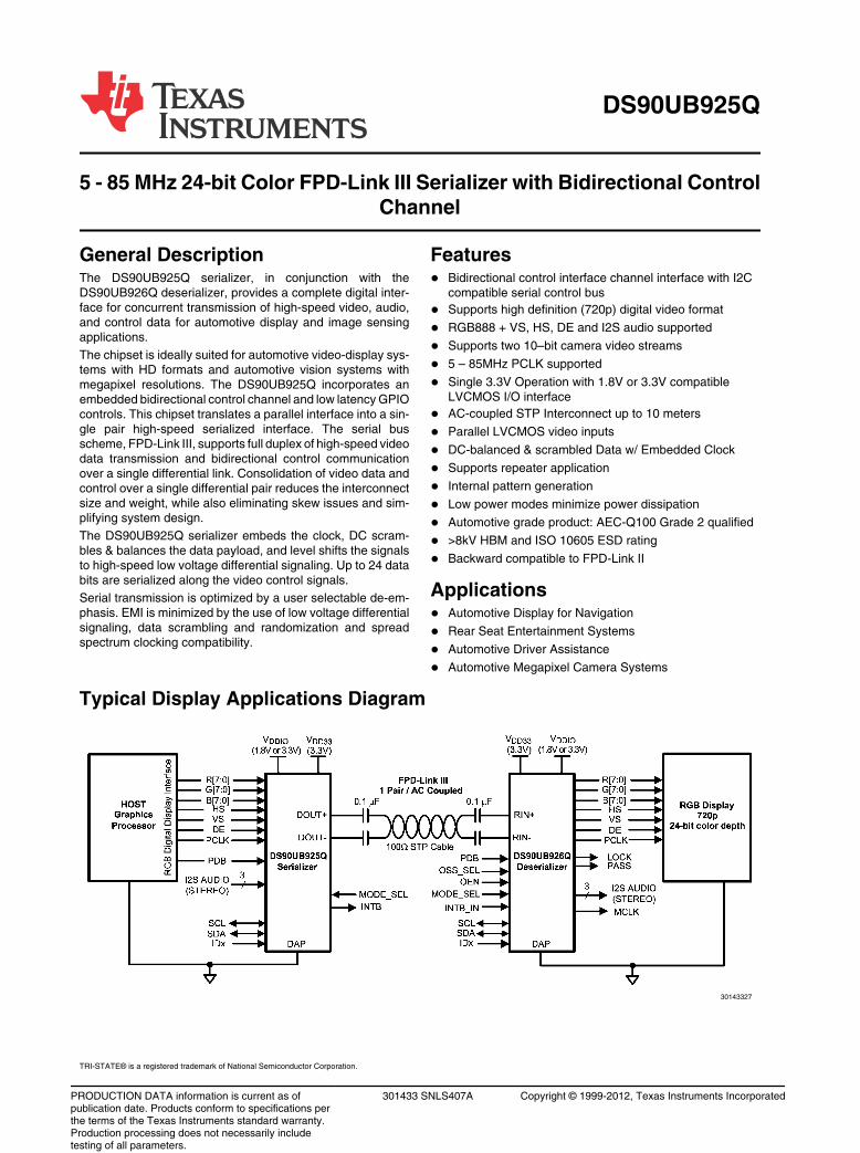
Typical Camera Applications Diagram
30143326
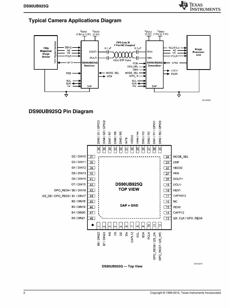
DS90UB925Q Pin Diagram
30143319
DS90UB925Q — Top View
DS90UB925Q
2 Copyright © 1999-2012, Texas Instruments Incorporated
Pin Descriptions
Pin Name Pin # I/O, Type Description
LVCMOS Parallel Interface
DIN[23:0] / R
[7:0], G[7:0],
B[7:0]
25, 26, 27, 28,
29, 32, 33, 34,
35, 36, 37, 38,
39, 40, 41, 42,
43, 44, 45, 46,
47, 48, 1, 2
I, LVCMOS
w/ pull down
Parallel Interface Data Input Pins
Leave open if unused
DIN0 / R0 can optionally be used as GPIO0 and DIN1 / R1 can optionally be used as GPIO1
DIN8 / G0 can optionally be used as GPIO2 and DIN9 /G1 can optionally be used as GPIO3
DIN16 / B0 can optionally be used as GPIO4 and DIN17 / B1 can optionally be used as
GPIO5
HS 3 I, LVCMOS
w/ pull down
Horizontal Sync Input Pin
Video control signal pulse width must be 3 PCLKs or longer to be transmitted when the
Control Signal Filter is enabled. There is no restriction on the minimum transition pulse
when the Control Signal Filter is disabled. The signal is limited to 2 transitions per 130
PCLKs.
See Table 6
VS 4 I, LVCMOS
w/ pull down
Vertical Sync Input Pin
Video control signal is limited to 1 transition per 130 PCLKs. Thus, the minimum pulse width
is 130 PCLKs.
DE 5 I, LVCMOS
w/ pull down
Data Enable Input Pin
Video control signal pulse width must be 3 PCLKs or longer to be transmitted when the
Control Signal Filter is enabled. There is no restriction on the minimum transition pulse
when the Control Signal Filter is disabled. The signal is limited to 2 transitions per 130
PCLKs.
See Table 6
PCLK 10 I, LVCMOS
w/ pull down
Pixel Clock Input Pin. Strobe edge set by RFB configuration register. SeeTable 6
I2S_CLK,
I2S_WC,
I2S_DA
13, 12, 11 I, LVCMOS
w/ pull down
Digital Audio Interface Data Input Pins
Leave open if unused
I2S_CLK can optionally be used as GPO_REG8, I2S_WC can optionally be used as
GPO_REG7, and I2S_DA can optionally be used as GPO_REG6.
Optional Parallel Interface
I2S_DB 44 I, LVCMOS
w/ pull down
Second Channel Digital Audio Interface Data Input pin at 18–bit color mode and set by
MODE_SEL pin or configuration register
Leave open if unused
I2S_DB can optionally be used as DIN17 or GPO_REG5.
GPIO[3:0] 36, 35, 26, 25 I/O,
LVCMOS
w/ pull down
General Purpose IOs. Available only in 18-bit color mode, and set by MODE_SEL pin or
configuration register. SeeTable 6
Leave open if unused
Shared with DIN9, DIN8, DIN1 and DIN0
GPO_REG
[8:4]
13, 12, 11, 44,
43
O, LVCMOS
w/ pull down
General Purpose Outputs and set by configuration register. See Table 6
Share with I2S_CLK, I2S_WC, I2S_DA, I2S_DB or DIN17, DIN16.
Optional Parallel Interface
PDB 21 I, LVCMOS
w/ pull-down
Power-down Mode Input Pin
PDB = H, device is enabled (normal operation)
Refer to ”Power Up Requirements and PDB Pin” in the Applications Information Section.
PDB = L, device is powered down.
When the device is in the powered down state, the Driver Outputs are both HIGH, the PLL
is shutdown, and IDD is minimized. Control Registers are RESET.
MODE_SEL 24 I, Analog Device Configuration Select. See Table 1
IDx 6 I, Analog I2C Serial Control Bus Device ID Address Select
External pull-up to VDD33 is required under all conditions, DO NOT FLOAT.
Connect to external pull-up and pull-down resistor to create a voltage divider. See Figure
17
DS90UB925Q
Copyright © 1999-2012, Texas Instruments Incorporated 3
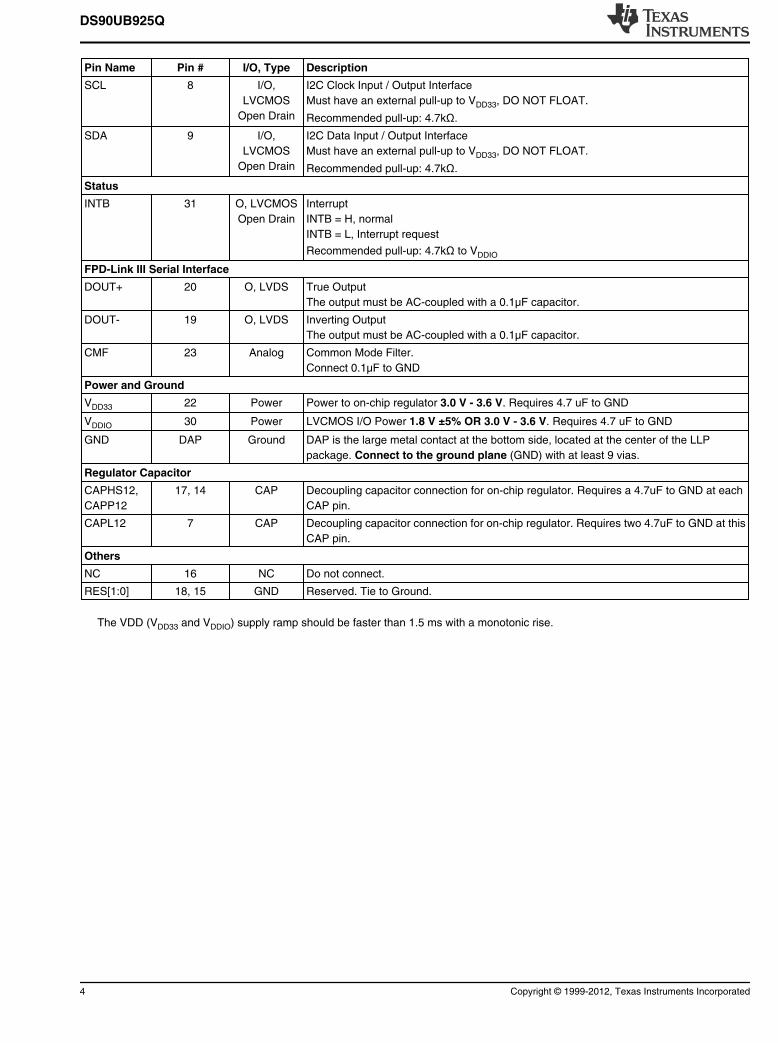
Pin Name Pin # I/O, Type Description
SCL 8 I/O,
LVCMOS
Open Drain
I2C Clock Input / Output Interface
Must have an external pull-up to VDD33, DO NOT FLOAT.
Recommended pull-up: 4.7kΩ.SDA 9 I/O,
LVCMOS
Open Drain
I2C Data Input / Output Interface
Must have an external pull-up to VDD33, DO NOT FLOAT.
Recommended pull-up: 4.7kΩ.Status
INTB 31 O, LVCMOS
Open Drain
Interrupt
INTB = H, normal
INTB = L, Interrupt request
Recommended pull-up: 4.7kΩ to VDDIO
FPD-Link III Serial Interface
DOUT+ 20 O, LVDS True Output
The output must be AC-coupled with a 0.1µF capacitor.
DOUT- 19 O, LVDS Inverting Output
The output must be AC-coupled with a 0.1µF capacitor.
CMF 23 Analog Common Mode Filter.
Connect 0.1µF to GND
Power and Ground
VDD33 22 Power Power to on-chip regulator 3.0 V - 3.6 V. Requires 4.7 uF to GND
VDDIO 30 Power LVCMOS I/O Power 1.8 V ±5% OR 3.0 V - 3.6 V. Requires 4.7 uF to GND
GND DAP Ground DAP is the large metal contact at the bottom side, located at the center of the LLP
package. Connect to the ground plane (GND) with at least 9 vias.
Regulator Capacitor
CAPHS12,
CAPP12
17, 14 CAP Decoupling capacitor connection for on-chip regulator. Requires a 4.7uF to GND at each
CAP pin.
CAPL12 7 CAP Decoupling capacitor connection for on-chip regulator. Requires two 4.7uF to GND at this
CAP pin.
Others
NC 16 NC Do not connect.
RES[1:0] 18, 15 GND Reserved. Tie to Ground.
The VDD (VDD33 and VDDIO) supply ramp should be faster than 1.5 ms with a monotonic rise.
DS90UB925Q
4 Copyright © 1999-2012, Texas Instruments Incorporated
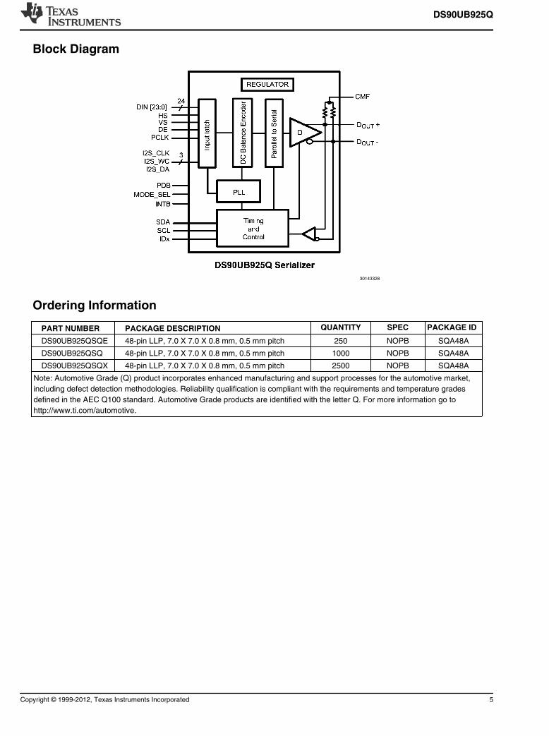
Block Diagram
30143328
Ordering Information
PART NUMBER PACKAGE DESCRIPTION QUANTITY SPEC PACKAGE ID
DS90UB925QSQE 48-pin LLP, 7.0 X 7.0 X 0.8 mm, 0.5 mm pitch 250 NOPB SQA48A
DS90UB925QSQ 48-pin LLP, 7.0 X 7.0 X 0.8 mm, 0.5 mm pitch 1000 NOPB SQA48A
DS90UB925QSQX 48-pin LLP, 7.0 X 7.0 X 0.8 mm, 0.5 mm pitch 2500 NOPB SQA48A
Note: Automotive Grade (Q) product incorporates enhanced manufacturing and support processes for the automotive market,
including defect detection methodologies. Reliability qualification is compliant with the requirements and temperature grades
defined in the AEC Q100 standard. Automotive Grade products are identified with the letter Q. For more information go to
http://www.ti.com/automotive.
DS90UB925Q
Copyright © 1999-2012, Texas Instruments Incorporated 5
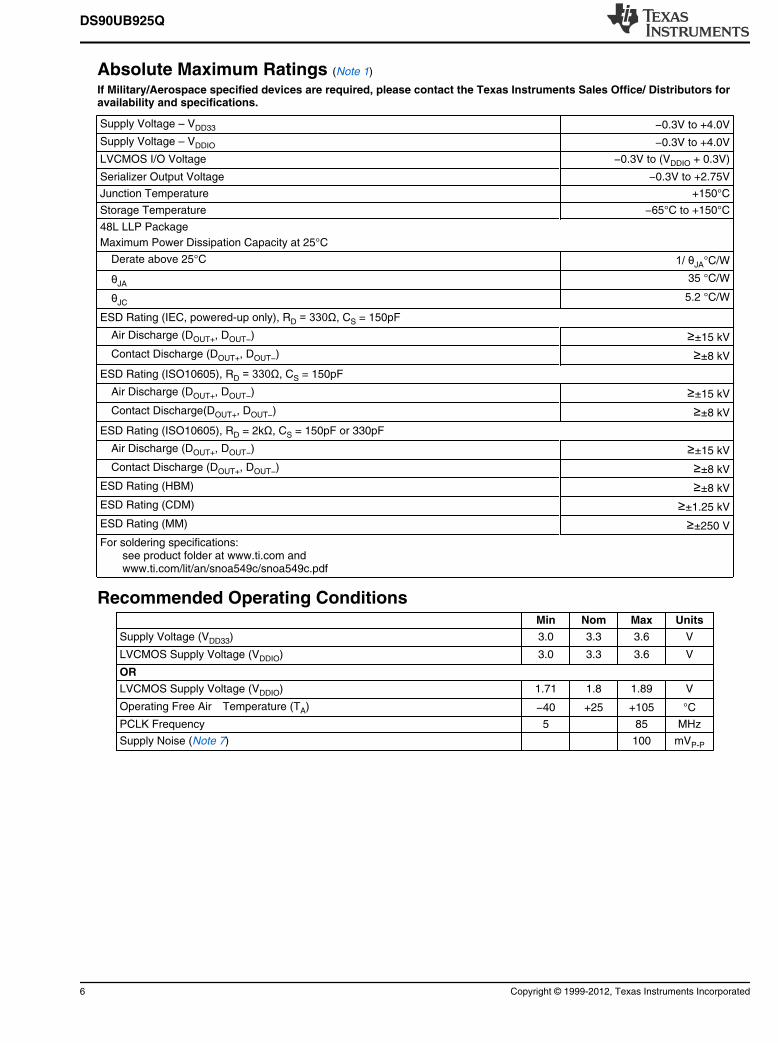
Absolute Maximum Ratings (Note 1)
If Military/Aerospace specified devices are required, please contact the Texas Instruments Sales Office/ Distributors foravailability and specifications.
Supply Voltage – VDD33 −0.3V to +4.0V
Supply Voltage – VDDIO −0.3V to +4.0V
LVCMOS I/O Voltage −0.3V to (VDDIO + 0.3V)
Serializer Output Voltage −0.3V to +2.75V
Junction Temperature +150°C
Storage Temperature −65°C to +150°C
48L LLP Package
Maximum Power Dissipation Capacity at 25°C
Derate above 25°C 1/ θJA°C/W
θJA35 °C/W
θJC5.2 °C/W
ESD Rating (IEC, powered-up only), RD = 330Ω, CS = 150pF
Air Discharge (DOUT+, DOUT−) ≥±15 kV
Contact Discharge (DOUT+, DOUT−) ≥±8 kV
ESD Rating (ISO10605), RD = 330Ω, CS = 150pF
Air Discharge (DOUT+, DOUT−) ≥±15 kV
Contact Discharge(DOUT+, DOUT−) ≥±8 kV
ESD Rating (ISO10605), RD = 2kΩ, CS = 150pF or 330pF
Air Discharge (DOUT+, DOUT−) ≥±15 kV
Contact Discharge (DOUT+, DOUT−) ≥±8 kV
ESD Rating (HBM) ≥±8 kV
ESD Rating (CDM) ≥±1.25 kV
ESD Rating (MM) ≥±250 V
For soldering specifications: see product folder at www.ti.com and www.ti.com/lit/an/snoa549c/snoa549c.pdf
Recommended Operating Conditions Min Nom Max Units
Supply Voltage (VDD33) 3.0 3.3 3.6 V
LVCMOS Supply Voltage (VDDIO) 3.0 3.3 3.6 V
OR
LVCMOS Supply Voltage (VDDIO) 1.71 1.8 1.89 V
Operating Free Air Temperature (TA) −40 +25 +105 °C
PCLK Frequency 5 85 MHz
Supply Noise (Note 7) 100 mVP-P
DS90UB925Q
6 Copyright © 1999-2012, Texas Instruments Incorporated
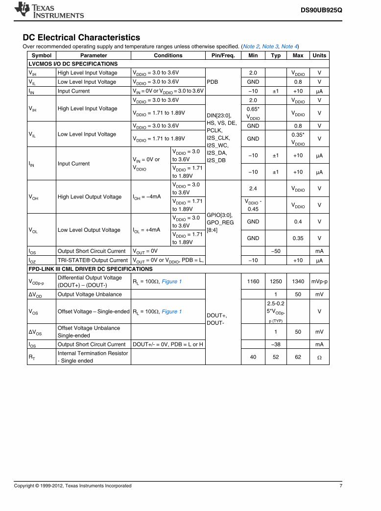
DC Electrical CharacteristicsOver recommended operating supply and temperature ranges unless otherwise specified. (Note 2, Note 3, Note 4)
Symbol Parameter Conditions Pin/Freq. Min Typ Max Units
LVCMOS I/O DC SPECIFICATIONS
VIH High Level Input Voltage VDDIO = 3.0 to 3.6V
PDB
2.0 VDDIO V
VIL Low Level Input Voltage VDDIO = 3.0 to 3.6V GND 0.8 V
IIN Input Current VIN = 0V or VDDIO = 3.0 to 3.6V −10 ±1 +10 μA
VIH High Level Input Voltage
VDDIO = 3.0 to 3.6V
DIN[23:0],
HS, VS, DE,
PCLK,
I2S_CLK,
I2S_WC,
I2S_DA,
I2S_DB
2.0 VDDIO V
VDDIO = 1.71 to 1.89V0.65*
VDDIO
VDDIO V
VIL Low Level Input Voltage
VDDIO = 3.0 to 3.6V GND 0.8 V
VDDIO = 1.71 to 1.89V GND 0.35*
VDDIO
V
IIN Input CurrentVIN = 0V or
VDDIO
VDDIO = 3.0
to 3.6V−10 ±1 +10 μA
VDDIO = 1.71
to 1.89V−10 ±1 +10 μA
VOH High Level Output Voltage IOH = −4mA
VDDIO = 3.0
to 3.6V
GPIO[3:0],
GPO_REG
[8:4]
2.4 VDDIO V
VDDIO = 1.71
to 1.89V
VDDIO -
0.45 VDDIO V
VOL Low Level Output Voltage IOL = +4mA
VDDIO = 3.0
to 3.6VGND 0.4 V
VDDIO = 1.71
to 1.89VGND 0.35 V
IOS Output Short Circuit Current VOUT = 0V −50 mA
IOZ TRI-STATE® Output Current VOUT = 0V or VDDIO, PDB = L, −10 +10 μA
FPD-LINK III CML DRIVER DC SPECIFICATIONS
VODp-p
Differential Output Voltage
(DOUT+) – (DOUT-)RL = 100Ω, Figure 1
DOUT+,
DOUT-
1160 1250 1340 mVp-p
ΔVOD Output Voltage Unbalance 1 50 mV
VOS Offset Voltage – Single-ended RL = 100Ω, Figure 1
2.5-0.2
5*VODp-
p (TYP)
V
ΔVOS
Offset Voltage Unbalance
Single-ended 1 50 mV
IOS Output Short Circuit Current DOUT+/- = 0V, PDB = L or H −38 mA
RT
Internal Termination Resistor
- Single ended 40 52 62 Ω
DS90UB925Q
Copyright © 1999-2012, Texas Instruments Incorporated 7
Symbol Parameter Conditions Pin/Freq. Min Typ Max Units
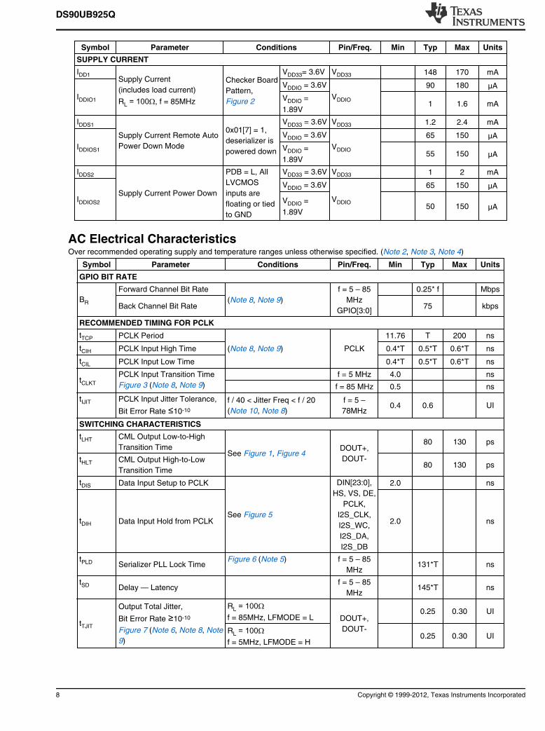
SUPPLY CURRENT
IDD1Supply Current
(includes load current)
RL = 100Ω, f = 85MHz
Checker Board
Pattern,
Figure 2
VDD33= 3.6V VDD33 148 170 mA
IDDIO1
VDDIO = 3.6V
VDDIO
90 180 μA
VDDIO =
1.89V 1 1.6 mA
IDDS1
Supply Current Remote Auto
Power Down Mode
0x01[7] = 1,
deserializer is
powered down
VDD33 = 3.6V VDD33 1.2 2.4 mA
IDDIOS1
VDDIO = 3.6V
VDDIO
65 150 μA
VDDIO =
1.89V 55 150 μA
IDDS2
Supply Current Power Down
PDB = L, All
LVCMOS
inputs are
floating or tied
to GND
VDD33 = 3.6V VDD33 1 2 mA
IDDIOS2
VDDIO = 3.6V
VDDIO
65 150 μA
VDDIO =
1.89V 50 150 μA
AC Electrical CharacteristicsOver recommended operating supply and temperature ranges unless otherwise specified. (Note 2, Note 3, Note 4)
Symbol Parameter Conditions Pin/Freq. Min Typ Max Units
GPIO BIT RATE
BR
Forward Channel Bit Rate
(Note 8, Note 9)
f = 5 – 85
MHz
GPIO[3:0]
0.25* f Mbps
Back Channel Bit Rate 75 kbps
RECOMMENDED TIMING FOR PCLK
tTCP PCLK Period
(Note 8, Note 9) PCLK
11.76 T 200 ns
tCIH PCLK Input High Time 0.4*T 0.5*T 0.6*T ns
tCIL PCLK Input Low Time 0.4*T 0.5*T 0.6*T ns
tCLKT
PCLK Input Transition Time
Figure 3 (Note 8, Note 9)
f = 5 MHz 4.0 ns
f = 85 MHz 0.5 ns
tIJIT PCLK Input Jitter Tolerance,
Bit Error Rate ≤10-10
f / 40 < Jitter Freq < f / 20
(Note 10, Note 8)
f = 5 –
78MHz0.4 0.6 UI
SWITCHING CHARACTERISTICS
tLHT CML Output Low-to-High
Transition TimeSee Figure 1, Figure 4
DOUT+,
DOUT-
80 130 ps
tHLT CML Output High-to-Low
Transition Time 80 130 ps
tDIS Data Input Setup to PCLK
See Figure 5
DIN[23:0],
HS, VS, DE,
PCLK,
I2S_CLK,
I2S_WC,
I2S_DA,
I2S_DB
2.0 ns
tDIH Data Input Hold from PCLK 2.0 ns
tPLD Serializer PLL Lock TimeFigure 6 (Note 5) f = 5 – 85
MHz 131*T ns
tSD Delay — Latency f = 5 – 85
MHz 145*T ns
tTJIT
Output Total Jitter,
Bit Error Rate ≥10-10
Figure 7 (Note 6, Note 8, Note
9)
RL = 100Ωf = 85MHz, LFMODE = L DOUT+,
DOUT-
0.25 0.30 UI
RL = 100Ωf = 5MHz, LFMODE = H
0.25 0.30 UI
DS90UB925Q
8 Copyright © 1999-2012, Texas Instruments Incorporated
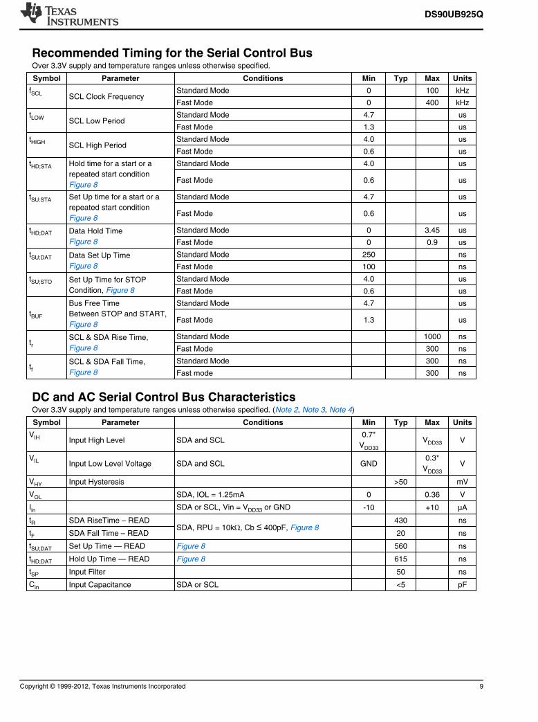
Recommended Timing for the Serial Control BusOver 3.3V supply and temperature ranges unless otherwise specified.
Symbol Parameter Conditions Min Typ Max Units
fSCL SCL Clock FrequencyStandard Mode 0 100 kHz
Fast Mode 0 400 kHz
tLOW SCL Low PeriodStandard Mode 4.7 us
Fast Mode 1.3 us
tHIGH SCL High PeriodStandard Mode 4.0 us
Fast Mode 0.6 us
tHD;STA Hold time for a start or a
repeated start condition
Figure 8
Standard Mode 4.0 us
Fast Mode 0.6 us
tSU:STA Set Up time for a start or a
repeated start condition
Figure 8
Standard Mode 4.7 us
Fast Mode 0.6 us
tHD;DAT Data Hold Time
Figure 8
Standard Mode 0 3.45 us
Fast Mode 0 0.9 us
tSU;DAT Data Set Up Time
Figure 8
Standard Mode 250 ns
Fast Mode 100 ns
tSU;STO Set Up Time for STOP
Condition, Figure 8
Standard Mode 4.0 us
Fast Mode 0.6 us
tBUF
Bus Free Time
Between STOP and START,
Figure 8
Standard Mode 4.7 us
Fast Mode 1.3 us
trSCL & SDA Rise Time,
Figure 8
Standard Mode 1000 ns
Fast Mode 300 ns
tfSCL & SDA Fall Time,
Figure 8
Standard Mode 300 ns
Fast mode 300 ns
DC and AC Serial Control Bus CharacteristicsOver 3.3V supply and temperature ranges unless otherwise specified. (Note 2, Note 3, Note 4)
Symbol Parameter Conditions Min Typ Max Units
VIH Input High Level SDA and SCL0.7*
VDD33
VDD33 V
VIL Input Low Level Voltage SDA and SCL GND 0.3*
VDD33
V
VHY Input Hysteresis >50 mV
VOL SDA, IOL = 1.25mA 0 0.36 V
Iin SDA or SCL, Vin = VDD33 or GND -10 +10 µA
tR SDA RiseTime – READSDA, RPU = 10kΩ, Cb ≤ 400pF, Figure 8
430 ns
tF SDA Fall Time – READ 20 ns
tSU;DAT Set Up Time — READ Figure 8 560 ns
tHD;DAT Hold Up Time — READ Figure 8 615 ns
tSP Input Filter 50 ns
Cin Input Capacitance SDA or SCL <5 pF
DS90UB925Q
Copyright © 1999-2012, Texas Instruments Incorporated 9
Note 1: “Absolute Maximum Ratings” indicate limits beyond which damage to the device may occur, including inoperability and degradation of device reliabilityand/or performance. Functional operation of the device and/or non-degradation at the Absolute Maximum Ratings or other conditions beyond those indicated inthe Recommended Operating Conditions is not implied. The Recommended Operating Conditions indicate conditions at which the device is functional and thedevice should not be operated beyond such conditions.
Note 2: The Electrical Characteristics tables list guaranteed specifications under the listed Recommended Operating Conditions except as otherwise modified orspecified by the Electrical Characteristics Conditions and/or Notes. Typical specifications are estimations only and are not guaranteed.
Note 3: Typical values represent most likely parametric norms at VDD = 3.3V, Ta = +25 degC, and at the Recommended Operation Conditions at the time ofproduct characterization and are not guaranteed.
Note 4: Current into device pins is defined as positive. Current out of a device pin is defined as negative. Voltages are referenced to ground except VOD andΔVOD, which are differential voltages.
Note 5: tPLD is the time required by the device to obtain lock when exiting power-down state with an active PCLK.
Note 6: UI – Unit Interval is equivalent to one serialized data bit width (1UI = 1 / 35*PCLK). The UI scales with PCLK frequency.
Note 7: Supply noise testing was done with minimum capacitors on the PCB. A sinusoidal signal is AC coupled to the VDD33 and VDDIOsupplies with amplitude =100 mVp-p measured at the device VDD33 and VDDIO pins. Bit error rate testing of input to the Ser and output of the Des with 10 meter cable shows no error whenthe noise frequency on the Ser is less than 50MHz. The Des on the other hand shows no error when the noise frequency is less than 50 MHz.
Note 8: Specification is guaranteed by characterization and is not tested in production.
Note 9: Specification is guaranteed by design and is not tested in production.
Note 10: Jitter Frequency is specified in conjunction with DS90UB926 PLL bandwidth.
DS90UB925Q
10 Copyright © 1999-2012, Texas Instruments Incorporated
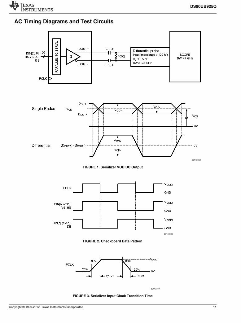
AC Timing Diagrams and Test Circuits
30143362
FIGURE 1. Serializer VOD DC Output
30143346
FIGURE 2. Checkboard Data Pattern
30143330
FIGURE 3. Serializer Input Clock Transition Time
DS90UB925Q
Copyright © 1999-2012, Texas Instruments Incorporated 11
30143347
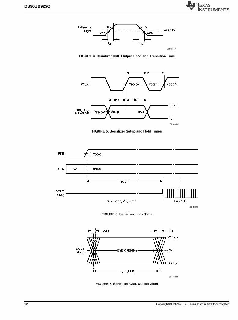
FIGURE 4. Serializer CML Output Load and Transition Time
30143361
FIGURE 5. Serializer Setup and Hold Times
30143349
FIGURE 6. Serializer Lock Time
30143348
FIGURE 7. Serializer CML Output Jitter
DS90UB925Q
12 Copyright © 1999-2012, Texas Instruments Incorporated
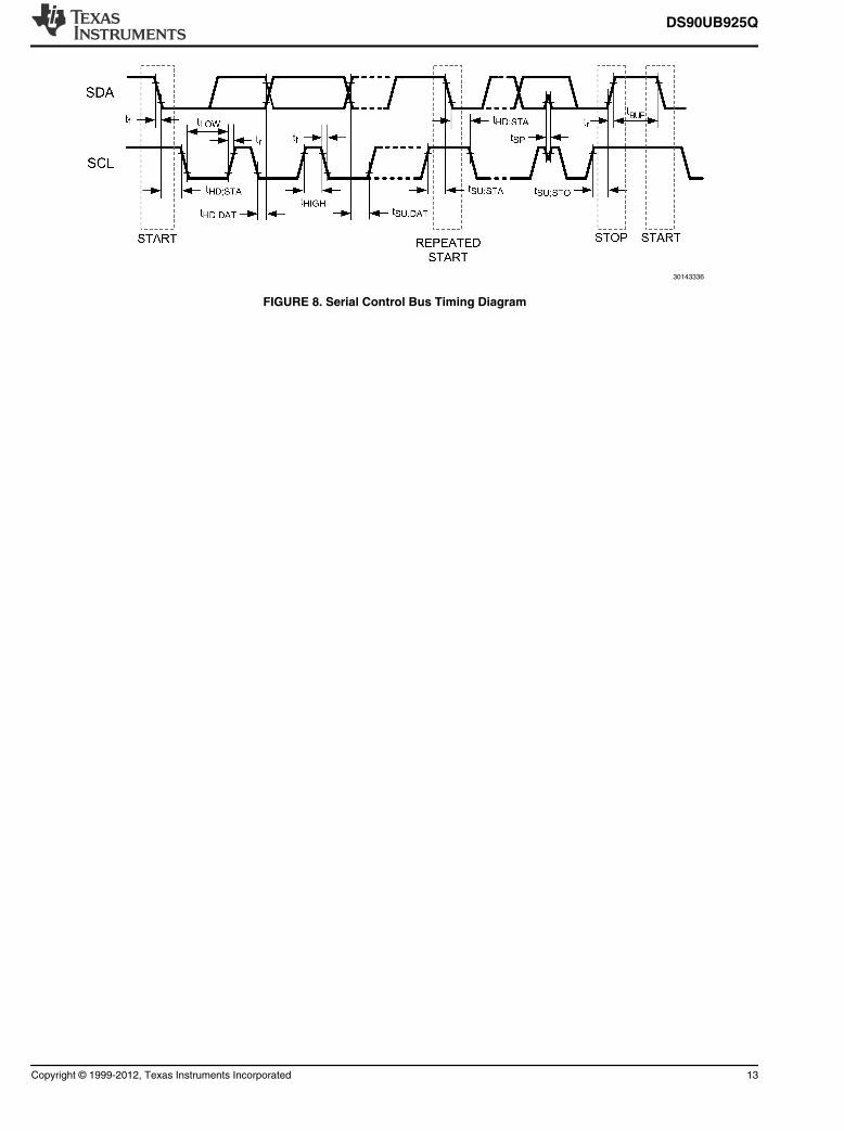
30143336
FIGURE 8. Serial Control Bus Timing Diagram
DS90UB925Q
Copyright © 1999-2012, Texas Instruments Incorporated 13
Functional DescriptionThe DS90UB925Q serializer transmits a 35-bit symbol over a single serial FPD-Link III pair operating up to 2.975 Gbps line rate.The serial stream contains an embedded clock, video control signals and DC-balanced video data and audio data which enhancesignal quality to support AC coupling. The serializer is intended for use with the DS90UB926Q deserializer, but is also backwardcompatible with DS90UR906Q or DS90UR908Q FPD-Link II deserializer.
The DS90UB925Q serializer and DS90UB926Q deserializer incorporate an I2C compatible interface. The I2C compatible interfaceallows programming of serializer or deserializer devices from a local host controller. In addition, the devices incorporate a bidirec-tional control channel (BCC) that allows communication between serializer/deserializer as well as remote I2C slave devices.
The bidirectional control channel is implemented via embedded signaling in the high-speed forward channel (serializer to deseri-alizer) as well as lower speed signaling in the reverse channel (deserializer to serializer). Through this interface, the BCC providesa mechanism to bridge I2C transactions across the serial link from one I2C bus to another. The implementation allows for arbitrationwith other I2C compatible masters at either side of the serial link.
There are two operating modes available on DS90UB925Q, display mode and camera mode. In display mode, I2C transactionsoriginate from the host controller attached to the serializer and target either the deserializer or an I2C slave attached to the dese-rializer. Transactions are detected by the I2C slave in the serializer and forwarded to the I2C master in the deserializer. Similarly,in camera mode, I2C transactions originate from a controller attached to the deserializer and target either the serializer or an I2Cslave attached to the serializer. Transactions are detected by the I2C slave in the deserializer and forwarded to the I2C master inthe serializer.
HIGH SPEED FORWARD CHANNEL DATA TRANSFER
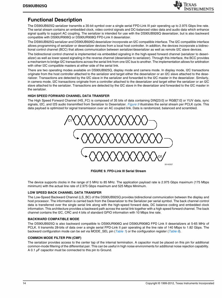
The High Speed Forward Channel (HS_FC) is composed of 35 bits of data containing DIN[23:0] or RGB[7:0] or YUV data, syncsignals, I2C, and I2S audio transmitted from Serializer to Deserializer. Figure 9 illustrates the serial stream per PCLK cycle. Thisdata payload is optimized for signal transmission over an AC coupled link. Data is randomized, balanced and scrambled.
30143337
FIGURE 9. FPD-Link III Serial Stream
The device supports clocks in the range of 5 MHz to 85 MHz. The application payload rate is 2.975 Gbps maximum (175 Mbpsminimum) with the actual line rate of 2.975 Gbps maximum and 525 Mbps Minimum.
LOW SPEED BACK CHANNEL DATA TRANSFER
The Low-Speed Backward Channel (LS_BC) of the DS90UB925Q provides bidirectional communication between the display andhost processor. The information is carried back from the Deserializer to the Serializer per serial symbol. The back channel controldata is transferred over the single serial link along with the high-speed forward data, DC balance coding and embedded clockinformation. This architecture provides a backward path across the serial link together with a high speed forward channel. The backchannel contains the I2C, CRC and 4 bits of standard GPIO information with 10 Mbps line rate.
BACKWARD COMPATIBLE MODE
The DS90UB925Q is also backward compatible to DS90UR906Q and DS90UR908Q FPD Link II deserializers at 5-65 MHz ofPCLK. It transmits 28-bits of data over a single serial FPD-Link II pair operating at the line rate of 140 Mbps to 1.82 Gbps. Thebackward configuration mode can be set via MODE_SEL pin (Table 1) or the configuration register (Table 6).
COMMON MODE FILTER PIN (CMF)
The serializer provides access to the center tap of the internal termination. A capacitor must be placed on this pin for additionalcommon-mode filtering of the differential pair. This can be useful in high noise environments for additional noise rejection capability.A 0.1 μF capacitor must be connected to this pin to Ground.
DS90UB925Q
14 Copyright © 1999-2012, Texas Instruments Incorporated
VIDEO CONTROL SIGNAL FILTER
When operating the devices in Normal Mode, the Video Control Signals (DE, HS, VS) have the following restrictions:
• Normal Mode with Control Signal Filter Enabled: DE and HS — Only 2 transitions per 130 clock cycles are transmitted, thetransition pulse must be 3 PCLK or longer.
• Normal Mode with Control Signal Filter Disabled: DE and HS — Only 2 transitions per 130 clock cycles are transmitted, norestriction on minimum transition pulse.
• VS — Only 1 transition per 130 clock cycles are transmitted, minimum pulse width is 130 clock cycles.
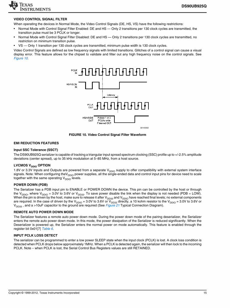
Video Control Signals are defined as low frequency signals with limited transitions. Glitches of a control signal can cause a visualdisplay error. This feature allows for the chipset to validate and filter out any high frequency noise on the control signals. SeeFigure 10.
30143302
FIGURE 10. Video Control Signal Filter Waveform
EMI REDUCTION FEATURES
Input SSC Tolerance (SSCT)
The DS90UB925Q serializer is capable of tracking a triangular input spread spectrum clocking (SSC) profile up to +/-2.5% amplitudedeviations (center spread), up to 35 kHz modulation at 5–85 MHz, from a host source.
LVCMOS VDDIO OPTION
1.8V or 3.3V Inputs and Outputs are powered from a separate VDDIO supply to offer compatibility with external system interfacesignals. Note: When configuring theVDDIO power supplies, all the single-ended data and control input pins for device need to scaletogether with the same operating VDDIO levels.
POWER DOWN (PDB)
The Serializer has a PDB input pin to ENABLE or POWER DOWN the device. This pin can be controlled by the host or throughthe VDDIO, where VDDIO = 3.0V to 3.6V or VDD33. To save power disable the link when the display is not needed (PDB = LOW).When the pin is driven by the host, make sure to release it after VDD33 and VDDIO have reached final levels; no external componentsare required. In the case of driven by the VDDIO = 3.0V to 3.6V or VDD33 directly, a 10 kohm resistor to the VDDIO = 3.0V to 3.6V orVDD33 , and a >10uF capacitor to the ground are required (See Figure 21 Typical Connection Diagram).
REMOTE AUTO POWER DOWN MODE
The Serializer features a remote auto power down mode. During the power down mode of the pairing deserializer, the Serializerenters the remote auto power down mode. In this mode, the power dissipation of the Serializer is reduced significantly. When theDeserializer is powered up, the Serializer enters the normal power on mode automatically. This feature is enabled through theregister bit 0x01[7] Table 6.
INPUT PCLK LOSS DETECT
The serializer can be programmed to enter a low power SLEEP state when the input clock (PCLK) is lost. A clock loss condition isdetected when PCLK drops below approximately 1MHz. When a PCLK is detected again, the serializer will then lock to the incomingPCLK. Note – when PCLK is lost, the Serial Control Bus Registers values are still RETAINED.
DS90UB925Q
Copyright © 1999-2012, Texas Instruments Incorporated 15
SERIAL LINK FAULT DETECT
The serial link fault detection is able to detect any of following seven (7) conditions
1) cable open
2) “+” to “-“ short
3) “+” short to GND
4) “-“ short to GND
5) “+” short to battery
6) “-“ short to battery
7) Cable is linked correctly
If any one of the fault conditions occurs, The Link Detect Status is 0 (cable is not detected) on bit 0 of address 0x0C Table 6.
PIXEL CLOCK EDGE SELECT (RFB)
The RFB control register bit selects which edge of the Pixel Clock is used. For the serializer, this pin determines the edge that thedata is latched on. If RFB is HIGH (‘1’), data is latched on the Rising edge of the PCLK. If RFB is LOW (‘0’), data is latched on theFalling edge of the PCLK.
LOW FREQUENCY OPTIMIZATION (LFMODE)
The LFMODE is set via register (0x04[1:0]) or MODE_SEL Pin 24 (Table 1). It controls the operating frequency of the serializer. IfLFMODE is Low (default), the PCLK frequency is between 15 MHz and 85 MHz. If LFMODE is High, the PCLK frequency is between5 MHz and <15 MHz. Please note when the device LFMODE is changed, a PDB reset is required.
INTERRUPT PIN — FUNCTIONAL DESCRIPTION AND USAGE (INTB)
1. On DS90UB925, set register 0xC6[5] = 1 and 0xC6[0] = 1
2. DS90UB926Q deserializer INTB_IN (pin 16) is set LOW by some downstream device.
3. DS90UB925Q serializer pulls INTB (pin 31) LOW. The signal is active low, so a LOW indicates an interrupt condition.
4. External controller detects INTB = LOW; to determine interrupt source, read ISR register .
5. A read to ISR will clear the interrupt at the DS90UB925, releasing INTB.
6. The external controller typically must then access the remote device to determine downstream interrupt source and clear theinterrupt driving INTB_IN. This would be when the downstream device releases the INTB_IN (pin 16) on the DS90UB926Q.The system is now ready to return to step (1) at next falling edge of INTB_IN.
CONFIGURATION SELECT (MODE_SEL)
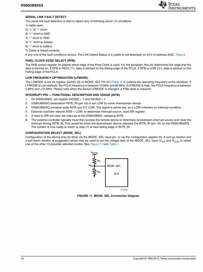
Configuration of the device may be done via the MODE_SEL input pin, or via the configuration register bit. A pull-up resistor anda pull-down resistor of suggested values may be used to set the voltage ratio of the MODE_SEL input (VR4) and VDD33 to selectone of the other 10 possible selected modes. See Figure 11 and Table 1.
30143341
FIGURE 11. MODE_SEL Connection Diagram
DS90UB925Q
16 Copyright © 1999-2012, Texas Instruments Incorporated
TABLE 1. Configuration Select (MODE_SEL)
# Ideal Ratio
VR4/VDD33
Ideal VR4
(V)
Suggested
Resistor R3
kΩ (1% tol)
Suggested
Resistor R4
kΩ (1% tol)
LFMODE Repeater Backward
Compatible
I2S Channel
B
(18–bit
Mode)
1 0 0 Open 40.2 or Any L L L L
2 0.121 0.399 294 40.2 L L L H
3 0.152 0.502 280 49.9 L H L L
4 0.242 0.799 240 76.8 L H L H
5 0.311 1.026 226 102 H L L L
6 0.402 1.327 196 130 H L L H
7 0.492 1.624 169 165 H H L L
8 0.583 1.924 137 191 H H L H
9 0.629 2.076 124 210 L L H L
10 0.727 2.399 90.9 243 H L H L
LFMODE: L = 15 – 85 MHz (Default); H = 5 – <15 MHz
Repeater: L = Repeater Off (Default); H = Repeater On
Backward Compatible: L = Backward Compatible Off (Default); H = Backward Compatible On to 906/908 (15 - 65MHz)
I2S Channel B: L = I2S Channel B Off, Normal 24-bit RGB Mode (Default); H = I2S Channel B On, 18-bit RGB Mode with I2S_DB
Enabled.
GPIO[3:0] and GPO_REG[8:4]
In 18-bit RGB operation mode, the optional R[1:0] and G[1:0] of the DS90UB925Q can be used as the general purpose IOs GPIO[3:0] in either forward channel (Inputs) or back channel (Outputs) application.
GPIO[3:0] Enable Sequence
See Table 2 for the GPIO enable sequencing.
Step 1: Enable the 18-bit mode either through the configuration register bit Table 6 on DS90UB925Q only. DS90UB926Q isautomatically configured as in the 18-bit mode.
Step 2: To enable GPIO3 forward channel, write 0x03 to address 0x0F on DS90UB925Q, then write 0x05 to address 0x1F onDS90UB926Q.
TABLE 2. GPIO Enable Sequencing Table
# Description Device Forward Channel Back Channel
1 Enable 18-bit
mode
DS90UB925Q 0x12 = 0x04 0x12 = 0x04
DS90UB926Q Auto Load from DS90UB925Q Auto Load from DS90UB925Q
2 GPIO3 DS90UB925Q 0x0F = 0x03 0x0F = 0x05
DS90UB926Q 0x1F = 0x05 0x1F = 0x03
3 GPIO2 DS90UB925Q 0x0E = 0x30 0x0E = 0x50
DS90UB926Q 0x1E = 0x50 0x1E = 0x30
4 GPIO1 DS90UB925Q 0x0E = 0x03 0x0E = 0x05
DS90UB926Q 0x1E = 0x05 0x0E = 0x05
5 GPIO0 DS90UB925Q 0x0D = 0x93 0x0D = 0x95
DS90UB926Q 0x1D = 0x95 0x1D = 0x93
GPO_REG[8:4] Enable Sequence
GPO_REG[8:4] are the outputs only pins. They must be programmed through the local register bits. See Table 3 for the GPO_REGenable sequencing.
Step 1: Enable the 18-bit mode either through the configuration register bit on DS90UB925Q only. DS90UB926Q is automaticallyconfigured as in the 18-bit mode.
Step 2: To enable GPO_REG8 outputs an “1”, write 0x90 to address 0x11 on DS90UB925Q.
DS90UB925Q
Copyright © 1999-2012, Texas Instruments Incorporated 17
TABLE 3. GPO_REG Enable Sequencing Table
# Description Device Local Access Local Output
1 Enable 18-bit mode DS90UB925Q 0x12 = 0x04
2 GPO_REG8 DS90UB925Q 0x11 = 0x90 “1”
0x11 = 0x10 “0”
3 GPO_REG7 DS90UB925Q 0x11 = 0x09 “1”
0x11 = 0x01 “0”
4 GPO_REG6 DS90UB925Q 0x10 = 0x90 “1”
0x10 = 0x10 “0”
5 GPO_REG5 DS90UB925Q 0x10 = 0x09 “1”
0x10 = 0x01 “0”
6 GPO_REG4 DS90UB925Q 0x0F = 0x90 “1”
0x0F = 0x10 “0”
I2S TRANSMITTING
In normal 24-bit RGB operation mode, the DS90UB925Q supports 3 bits of I2S. They are I2S_CLK, I2S_WC and I2S_DA. Theoptionally packetized audio information can be transmitted during the video blanking (data island transport) or during active video(forward channel frame transport).
Secondary I2S Channel
In I2S Channel B operation mode, the secondary I2S data (I2S_DB) can be used as the additional I2S audio in addition to the 3–bit of I2S. The I2S_DB input must be synchronized to I2S_CLK and aligned with I2S_DA and I2S_WC at the input to the serializer.This operation mode is enabled through either the MODE_SEL pin (Table 1) or through the register bit 0x12[0] (Table 6).
Table 4 below covers the range of I2S sample rates.
TABLE 4. Audio Interface Frequencies
Sample Rate (kHz) I2S Data Word Size (bits) I2S CLK (MHz)
32 16 1.024
44.1 16 1.411
48 16 1.536
96 16 3.072
192 16 6.144
32 24 1.536
44.1 24 2.117
48 24 2.304
96 24 4.608
192 24 9.216
32 32 2.048
44.1 32 2.822
48 32 3.072
96 32 6.144
192 32 12.288
DS90UB925Q
18 Copyright © 1999-2012, Texas Instruments Incorporated
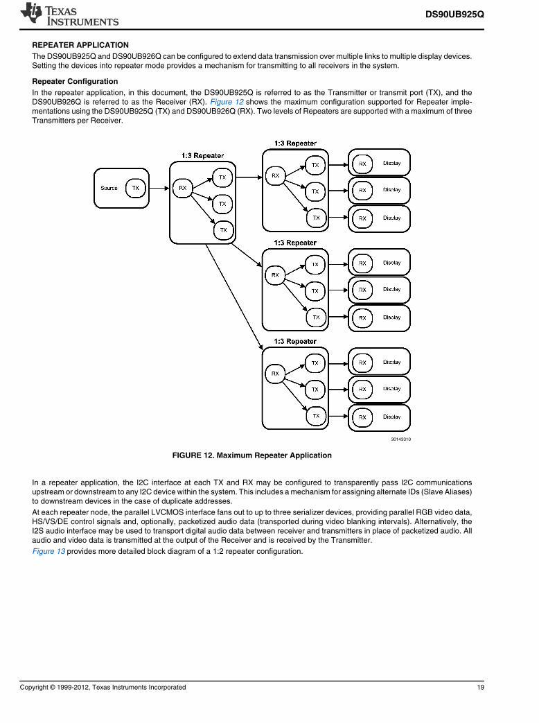
REPEATER APPLICATION
The DS90UB925Q and DS90UB926Q can be configured to extend data transmission over multiple links to multiple display devices.Setting the devices into repeater mode provides a mechanism for transmitting to all receivers in the system.
Repeater Configuration
In the repeater application, in this document, the DS90UB925Q is referred to as the Transmitter or transmit port (TX), and theDS90UB926Q is referred to as the Receiver (RX). Figure 12 shows the maximum configuration supported for Repeater imple-mentations using the DS90UB925Q (TX) and DS90UB926Q (RX). Two levels of Repeaters are supported with a maximum of threeTransmitters per Receiver.
30143310
FIGURE 12. Maximum Repeater Application
In a repeater application, the I2C interface at each TX and RX may be configured to transparently pass I2C communicationsupstream or downstream to any I2C device within the system. This includes a mechanism for assigning alternate IDs (Slave Aliases)to downstream devices in the case of duplicate addresses.
At each repeater node, the parallel LVCMOS interface fans out to up to three serializer devices, providing parallel RGB video data,HS/VS/DE control signals and, optionally, packetized audio data (transported during video blanking intervals). Alternatively, theI2S audio interface may be used to transport digital audio data between receiver and transmitters in place of packetized audio. Allaudio and video data is transmitted at the output of the Receiver and is received by the Transmitter.
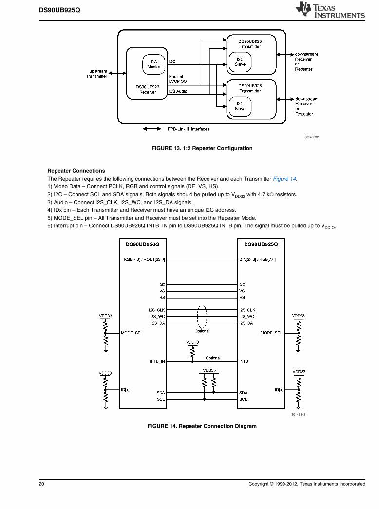
Figure 13 provides more detailed block diagram of a 1:2 repeater configuration.
DS90UB925Q
Copyright © 1999-2012, Texas Instruments Incorporated 19
30143332
FIGURE 13. 1:2 Repeater Configuration
Repeater Connections
The Repeater requires the following connections between the Receiver and each Transmitter Figure 14.
1) Video Data – Connect PCLK, RGB and control signals (DE, VS, HS).
2) I2C – Connect SCL and SDA signals. Both signals should be pulled up to VDD33 with 4.7 kΩ resistors.
3) Audio – Connect I2S_CLK, I2S_WC, and I2S_DA signals.
4) IDx pin – Each Transmitter and Receiver must have an unique I2C address.
5) MODE_SEL pin – All Transmitter and Receiver must be set into the Repeater Mode.
6) Interrupt pin – Connect DS90UB926Q INTB_IN pin to DS90UB925Q INTB pin. The signal must be pulled up to VDDIO.
30143342
FIGURE 14. Repeater Connection Diagram
DS90UB925Q
20 Copyright © 1999-2012, Texas Instruments Incorporated
BUILT IN SELF TEST (BIST)
An optional At-Speed Built In Self Test (BIST) feature supports the testing of the high speed serial link and the low- speed backchannel. This is useful in the prototype stage, equipment production, in-system test and also for system diagnostics.Note: BIST is not available in backwards compatible mode.
BIST Configuration and Status
The BIST mode is enabled at the deseralizer by the Pin select (Pin 44 BISTEN and Pin 16 BISTC) or configuration register(Table6) through the deserializer. When LFMODE = 0, the pin based configuration defaults to external PCLK or 33 MHz internal Oscillatorclock (OSC) frequency. In the absence of PCLK, the user can select the desired OSC frequency (default 33 MHz or 25MHz) throughthe register bit. When LFMODE = 1, the pin based configuration defaults to external PCLK or 12.5MHz MHz internal Oscillatorclock (OSC) frequency.
When BISTEN of the deserializer is high, the BIST mode enable information is sent to the serializer through the Back Channel.The serializer outputs a test pattern and drives the link at speed. The deserializer detects the test pattern and monitors it for errors.The PASS output pin toggles to flag any payloads that are received with 1 to 35 bit errors.
The BIST status is monitored real time on PASS pin. The result of the test is held on the PASS output until reset (new BIST testor Power Down). A high on PASS indicates NO ERRORS were detected. A Low on PASS indicates one or more errors weredetected. The duration of the test is controlled by the pulse width applied to the deserializer BISTEN pin. This BIST feature alsocontains a Link Error Count and a Lock Status. If the connection of the serial link is broken, then the link error count is shown inthe register. When the PLL of the deserializer is locked or unlocked, the lock status can be read in the register. See Table 6.
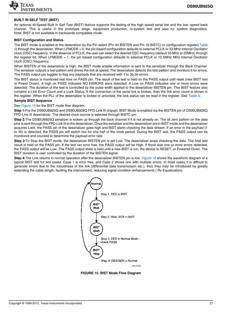
Sample BIST Sequence
See Figure 15 for the BIST mode flow diagram.
Step 1:For the DS90UB925Q and DS90UB926Q FPD-Link III chipset, BIST Mode is enabled via the BISTEN pin of DS90UB926QFPD-Link III deserializer. The desired clock source is selected through BISTC pin.
Step 2:The DS90UB925Q serializer is woken up through the back channel if it is not already on. The all zero pattern on the datapins is sent through the FPD-Link III to the deserializer. Once the serializer and the deserializer are in BIST mode and the deserializeracquires Lock, the PASS pin of the deserializer goes high and BIST starts checking the data stream. If an error in the payload (1to 35) is detected, the PASS pin will switch low for one half of the clock period. During the BIST test, the PASS output can bemonitored and counted to determine the payload error rate.
Step 3:To Stop the BIST mode, the deserializer BISTEN pin is set Low. The deserializer stops checking the data. The final testresult is held on the PASS pin. If the test ran error free, the PASS output will be High. If there was one or more errors detected,the PASS output will be Low. The PASS output state is held until a new BIST is run, the device is RESET, or Powered Down. TheBIST duration is user controlled by the duration of the BISTEN signal.
Step 4:The Link returns to normal operation after the deserializer BISTEN pin is low. Figure 16 shows the waveform diagram of atypical BIST test for two cases. Case 1 is error free, and Case 2 shows one with multiple errors. In most cases it is difficult togenerate errors due to the robustness of the link (differential data transmission etc.), thus they may be introduced by greatlyextending the cable length, faulting the interconnect, reducing signal condition enhancements ( Rx Equalization).
30143343
FIGURE 15. BIST Mode Flow Diagram
DS90UB925Q
Copyright © 1999-2012, Texas Instruments Incorporated 21
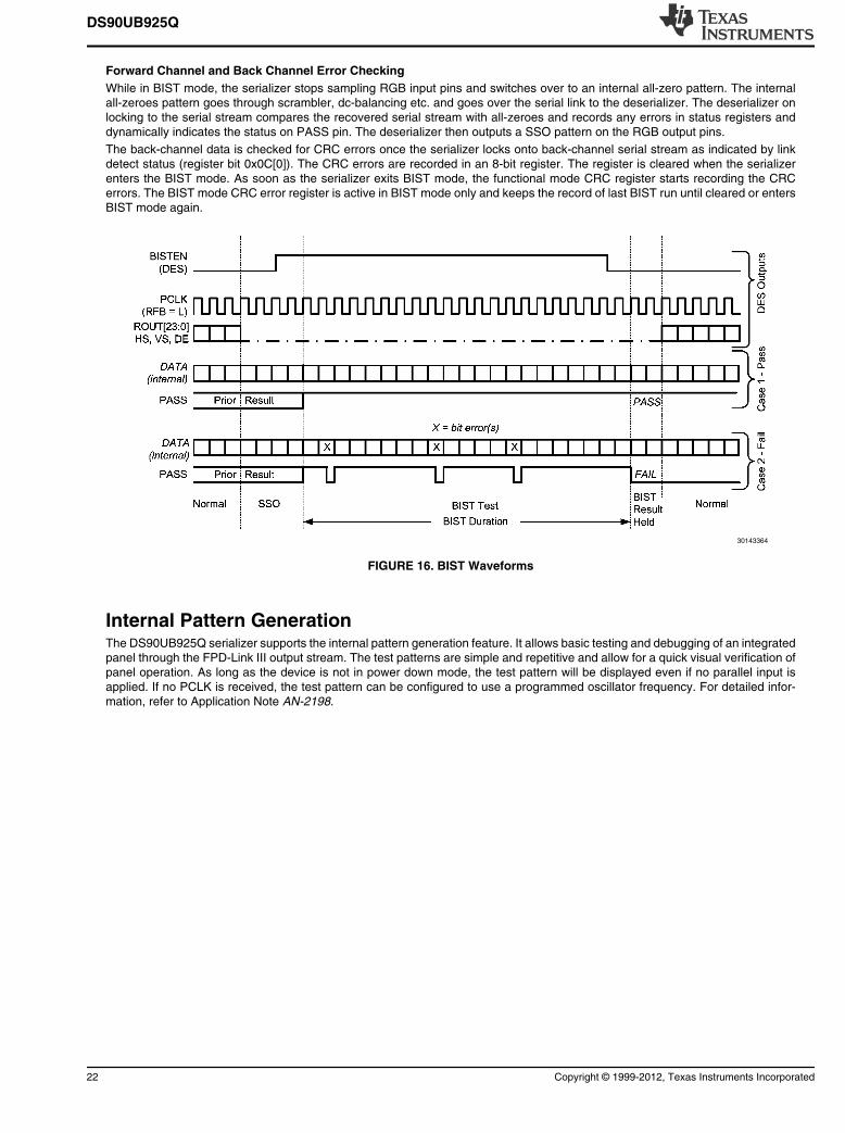
Forward Channel and Back Channel Error Checking
While in BIST mode, the serializer stops sampling RGB input pins and switches over to an internal all-zero pattern. The internalall-zeroes pattern goes through scrambler, dc-balancing etc. and goes over the serial link to the deserializer. The deserializer onlocking to the serial stream compares the recovered serial stream with all-zeroes and records any errors in status registers anddynamically indicates the status on PASS pin. The deserializer then outputs a SSO pattern on the RGB output pins.
The back-channel data is checked for CRC errors once the serializer locks onto back-channel serial stream as indicated by linkdetect status (register bit 0x0C[0]). The CRC errors are recorded in an 8-bit register. The register is cleared when the serializerenters the BIST mode. As soon as the serializer exits BIST mode, the functional mode CRC register starts recording the CRCerrors. The BIST mode CRC error register is active in BIST mode only and keeps the record of last BIST run until cleared or entersBIST mode again.
30143364
FIGURE 16. BIST Waveforms
Internal Pattern GenerationThe DS90UB925Q serializer supports the internal pattern generation feature. It allows basic testing and debugging of an integratedpanel through the FPD-Link III output stream. The test patterns are simple and repetitive and allow for a quick visual verification ofpanel operation. As long as the device is not in power down mode, the test pattern will be displayed even if no parallel input isapplied. If no PCLK is received, the test pattern can be configured to use a programmed oscillator frequency. For detailed infor-mation, refer to Application Note AN-2198.
DS90UB925Q
22 Copyright © 1999-2012, Texas Instruments Incorporated
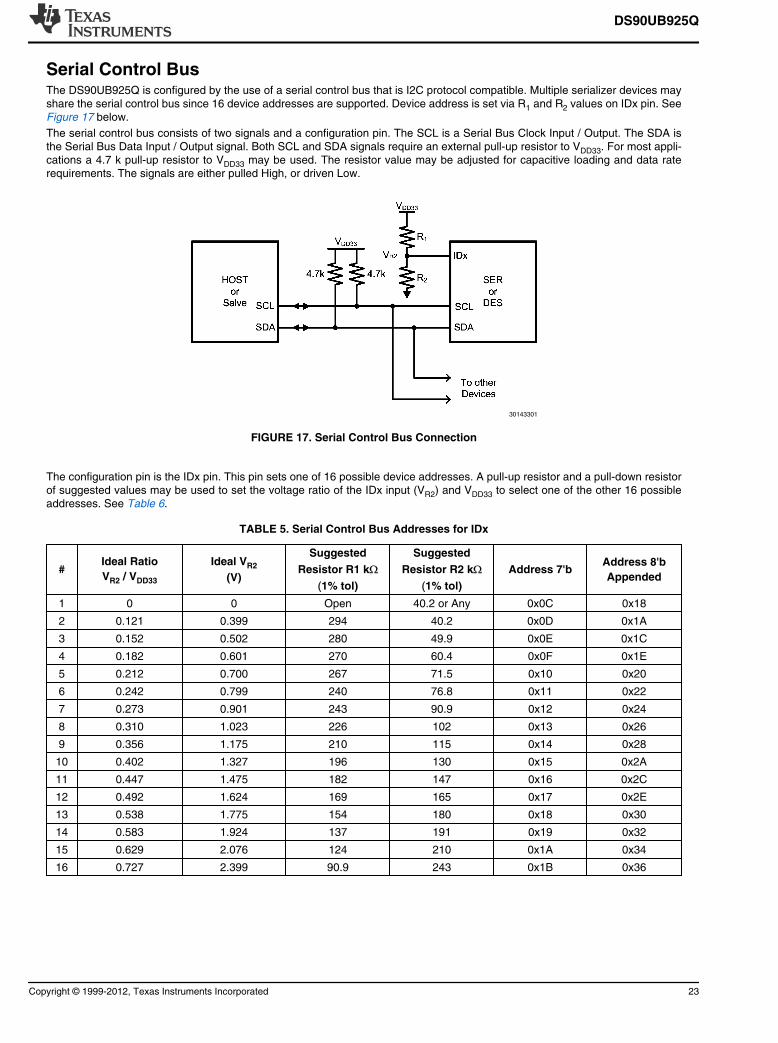
Serial Control BusThe DS90UB925Q is configured by the use of a serial control bus that is I2C protocol compatible. Multiple serializer devices mayshare the serial control bus since 16 device addresses are supported. Device address is set via R1 and R2 values on IDx pin. SeeFigure 17 below.
The serial control bus consists of two signals and a configuration pin. The SCL is a Serial Bus Clock Input / Output. The SDA isthe Serial Bus Data Input / Output signal. Both SCL and SDA signals require an external pull-up resistor to VDD33. For most appli-cations a 4.7 k pull-up resistor to VDD33 may be used. The resistor value may be adjusted for capacitive loading and data raterequirements. The signals are either pulled High, or driven Low.
30143301
FIGURE 17. Serial Control Bus Connection
The configuration pin is the IDx pin. This pin sets one of 16 possible device addresses. A pull-up resistor and a pull-down resistorof suggested values may be used to set the voltage ratio of the IDx input (VR2) and VDD33 to select one of the other 16 possibleaddresses. See Table 6.
TABLE 5. Serial Control Bus Addresses for IDx
#Ideal Ratio
VR2 / VDD33
Ideal VR2
(V)
Suggested
Resistor R1 kΩ(1% tol)
Suggested
Resistor R2 kΩ(1% tol)
Address 7'bAddress 8'b
Appended
1 0 0 Open 40.2 or Any 0x0C 0x18
2 0.121 0.399 294 40.2 0x0D 0x1A
3 0.152 0.502 280 49.9 0x0E 0x1C
4 0.182 0.601 270 60.4 0x0F 0x1E
5 0.212 0.700 267 71.5 0x10 0x20
6 0.242 0.799 240 76.8 0x11 0x22
7 0.273 0.901 243 90.9 0x12 0x24
8 0.310 1.023 226 102 0x13 0x26
9 0.356 1.175 210 115 0x14 0x28
10 0.402 1.327 196 130 0x15 0x2A
11 0.447 1.475 182 147 0x16 0x2C
12 0.492 1.624 169 165 0x17 0x2E
13 0.538 1.775 154 180 0x18 0x30
14 0.583 1.924 137 191 0x19 0x32
15 0.629 2.076 124 210 0x1A 0x34
16 0.727 2.399 90.9 243 0x1B 0x36
DS90UB925Q
Copyright © 1999-2012, Texas Instruments Incorporated 23
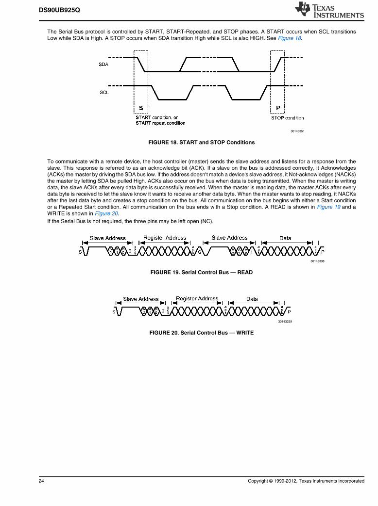
The Serial Bus protocol is controlled by START, START-Repeated, and STOP phases. A START occurs when SCL transitionsLow while SDA is High. A STOP occurs when SDA transition High while SCL is also HIGH. See Figure 18.
30143351
FIGURE 18. START and STOP Conditions
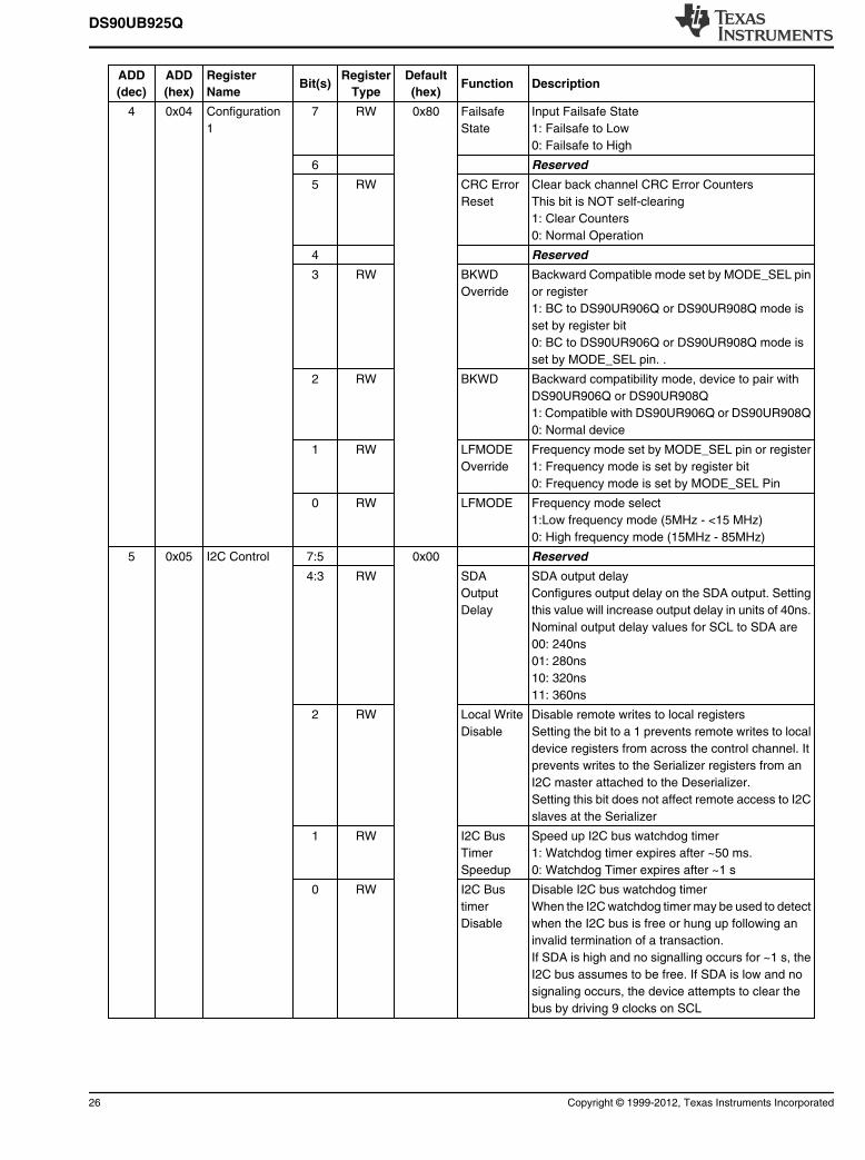
To communicate with a remote device, the host controller (master) sends the slave address and listens for a response from theslave. This response is referred to as an acknowledge bit (ACK). If a slave on the bus is addressed correctly, it Acknowledges(ACKs) the master by driving the SDA bus low. If the address doesn't match a device's slave address, it Not-acknowledges (NACKs)the master by letting SDA be pulled High. ACKs also occur on the bus when data is being transmitted. When the master is writingdata, the slave ACKs after every data byte is successfully received. When the master is reading data, the master ACKs after everydata byte is received to let the slave know it wants to receive another data byte. When the master wants to stop reading, it NACKsafter the last data byte and creates a stop condition on the bus. All communication on the bus begins with either a Start conditionor a Repeated Start condition. All communication on the bus ends with a Stop condition. A READ is shown in Figure 19 and aWRITE is shown in Figure 20.
If the Serial Bus is not required, the three pins may be left open (NC).
30143338
FIGURE 19. Serial Control Bus — READ
30143339
FIGURE 20. Serial Control Bus — WRITE
DS90UB925Q
24 Copyright © 1999-2012, Texas Instruments Incorporated
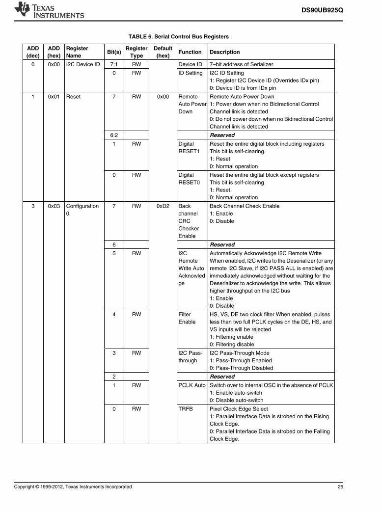
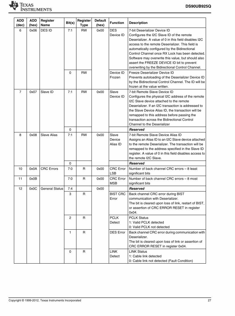
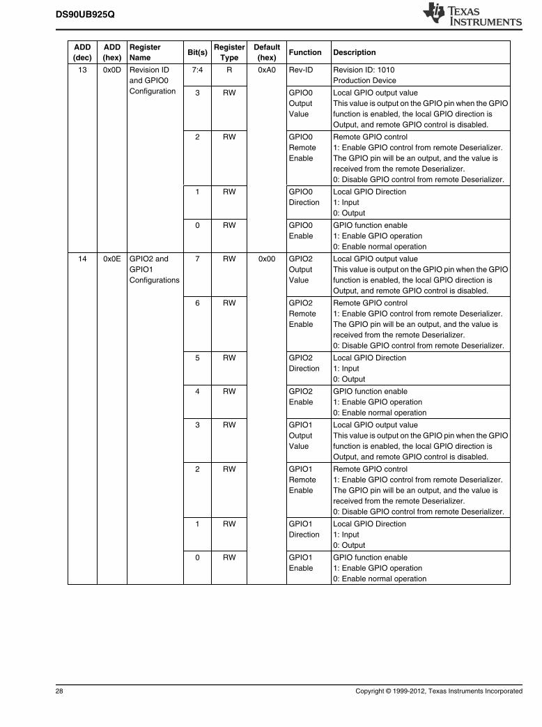
TABLE 6. Serial Control Bus Registers
ADD
(dec)
ADD
(hex)
Register
NameBit(s)
Register
Type
Default
(hex)Function Description
0 0x00 I2C Device ID 7:1 RW Device ID 7–bit address of Serializer
0 RW ID Setting I2C ID Setting
1: Register I2C Device ID (Overrides IDx pin)
0: Device ID is from IDx pin
1 0x01 Reset 7 RW 0x00 Remote
Auto Power
Down
Remote Auto Power Down
1: Power down when no Bidirectional Control
Channel link is detected
0: Do not power down when no Bidirectional Control
Channel link is detected
6:2 Reserved
1 RW Digital
RESET1
Reset the entire digital block including registers
This bit is self-clearing.
1: Reset
0: Normal operation
0 RW Digital
RESET0
Reset the entire digital block except registers
This bit is self-clearing
1: Reset
0: Normal operation
3 0x03 Configuration
0
7 RW 0xD2 Back
channel
CRC
Checker
Enable
Back Channel Check Enable
1: Enable
0: Disable
6 Reserved
5 RW I2C
Remote
Write Auto
Acknowled
ge
Automatically Acknowledge I2C Remote Write
When enabled, I2C writes to the Deserializer (or any
remote I2C Slave, if I2C PASS ALL is enabled) are
immediately acknowledged without waiting for the
Deserializer to acknowledge the write. This allows
higher throughput on the I2C bus
1: Enable
0: Disable
4 RW Filter
Enable
HS, VS, DE two clock filter When enabled, pulses
less than two full PCLK cycles on the DE, HS, and
VS inputs will be rejected
1: Filtering enable
0: Filtering disable
3 RW I2C Pass-
through
I2C Pass-Through Mode
1: Pass-Through Enabled
0: Pass-Through Disabled
2 Reserved
1 RW PCLK Auto Switch over to internal OSC in the absence of PCLK
1: Enable auto-switch
0: Disable auto-switch
0 RW TRFB Pixel Clock Edge Select
1: Parallel Interface Data is strobed on the Rising
Clock Edge.
0: Parallel Interface Data is strobed on the Falling
Clock Edge.
DS90UB925Q
Copyright © 1999-2012, Texas Instruments Incorporated 25
ADD
(dec)
ADD
(hex)
Register
NameBit(s)
Register
Type
Default
(hex)Function Description
4 0x04 Configuration
1
7 RW 0x80 Failsafe
State
Input Failsafe State
1: Failsafe to Low
0: Failsafe to High
6 Reserved
5 RW CRC Error
Reset
Clear back channel CRC Error Counters
This bit is NOT self-clearing
1: Clear Counters
0: Normal Operation
4 Reserved
3 RW BKWD
Override
Backward Compatible mode set by MODE_SEL pin
or register
1: BC to DS90UR906Q or DS90UR908Q mode is
set by register bit
0: BC to DS90UR906Q or DS90UR908Q mode is
set by MODE_SEL pin. .
2 RW BKWD Backward compatibility mode, device to pair with
DS90UR906Q or DS90UR908Q
1: Compatible with DS90UR906Q or DS90UR908Q
0: Normal device
1 RW LFMODE
Override
Frequency mode set by MODE_SEL pin or register
1: Frequency mode is set by register bit
0: Frequency mode is set by MODE_SEL Pin
0 RW LFMODE Frequency mode select
1:Low frequency mode (5MHz - <15 MHz)
0: High frequency mode (15MHz - 85MHz)
5 0x05 I2C Control 7:5 0x00 Reserved
4:3 RW SDA
Output
Delay
SDA output delay
Configures output delay on the SDA output. Setting
this value will increase output delay in units of 40ns.
Nominal output delay values for SCL to SDA are
00: 240ns
01: 280ns
10: 320ns
11: 360ns
2 RW Local Write
Disable
Disable remote writes to local registers
Setting the bit to a 1 prevents remote writes to local
device registers from across the control channel. It
prevents writes to the Serializer registers from an
I2C master attached to the Deserializer.
Setting this bit does not affect remote access to I2C
slaves at the Serializer
1 RW I2C Bus
Timer
Speedup
Speed up I2C bus watchdog timer
1: Watchdog timer expires after ~50 ms.
0: Watchdog Timer expires after ~1 s
0 RW I2C Bus
timer
Disable
Disable I2C bus watchdog timer
When the I2C watchdog timer may be used to detect
when the I2C bus is free or hung up following an
invalid termination of a transaction.
If SDA is high and no signalling occurs for ~1 s, the
I2C bus assumes to be free. If SDA is low and no
signaling occurs, the device attempts to clear the
bus by driving 9 clocks on SCL
DS90UB925Q
26 Copyright © 1999-2012, Texas Instruments Incorporated
ADD
(dec)
ADD
(hex)
Register
NameBit(s)
Register
Type
Default
(hex)Function Description
6 0x06 DES ID 7:1 RW 0x00 DES
Device ID
7-bit Deserializer Device ID
Configures the I2C Slave ID of the remote
Deserializer. A value of 0 in this field disables I2C
access to the remote Deserializer. This field is
automatically configured by the Bidirectional
Control Channel once RX Lock has been detected.
Software may overwrite this value, but should also
assert the FREEZE DEVICE ID bit to prevent
overwriting by the Bidirectional Control Channel.
0 RW Device ID
Frozen
Freeze Deserializer Device ID
Prevents autoloading of the Deserializer Device ID
by the Bidirectional Control Channel. The ID will be
frozen at the value written.
7 0x07 Slave ID 7:1 RW 0x00 Slave
Device ID
7-bit Remote Slave Device ID
Configures the physical I2C address of the remote
I2C Slave device attached to the remote
Deserializer. If an I2C transaction is addressed to
the Slave Device Alias ID, the transaction will be
remapped to this address before passing the
transaction across the Bidirectional Control
Channel to the Deserializer
0 Reserved
8 0x08 Slave Alias 7:1 RW 0x00 Slave
Device
Alias ID
7-bit Remote Slave Device Alias ID
Assigns an Alias ID to an I2C Slave device attached
to the remote Deserializer. The transaction will be
remapped to the address specified in the Slave ID
register. A value of 0 in this field disables access to
the remote I2C Slave.
0 Reserved
10 0x0A CRC Errors 7:0 R 0x00 CRC Error
LSB
Number of back channel CRC errors – 8 least
significant bits
11 0x0B 7:0 R 0x00 CRC Error
MSB
Number of back channel CRC errors – 8 most
significant bits
12 0x0C General Status 7:4 0x00 Reserved
3 R BIST CRC
Error
Back channel CRC error during BIST
communication with Deserializer.
The bit is cleared upon loss of link, restart of BIST,
or assertion of CRC ERROR RESET in register
0x04.
2 R PCLK
Detect
PCLK Status
1: Valid PCLK detected
0: Valid PCLK not detected
1 R DES Error Back channel CRC error during communication with
Deserializer.
The bit is cleared upon loss of link or assertion of
CRC ERROR RESET in register 0x04.
0 R LINK
Detect
LINK Status
1: Cable link detected
0: Cable link not detected (Fault Condition)
DS90UB925Q
Copyright © 1999-2012, Texas Instruments Incorporated 27
ADD
(dec)
ADD
(hex)
Register
NameBit(s)
Register
Type
Default
(hex)Function Description
13 0x0D Revision ID
and GPIO0
Configuration
7:4 R 0xA0 Rev-ID Revision ID: 1010
Production Device
3 RW GPIO0
Output
Value
Local GPIO output value
This value is output on the GPIO pin when the GPIO
function is enabled, the local GPIO direction is
Output, and remote GPIO control is disabled.
2 RW GPIO0
Remote
Enable
Remote GPIO control
1: Enable GPIO control from remote Deserializer.
The GPIO pin will be an output, and the value is
received from the remote Deserializer.
0: Disable GPIO control from remote Deserializer.
1 RW GPIO0
Direction
Local GPIO Direction
1: Input
0: Output
0 RW GPIO0
Enable
GPIO function enable
1: Enable GPIO operation
0: Enable normal operation
14 0x0E GPIO2 and
GPIO1
Configurations
7 RW 0x00 GPIO2
Output
Value
Local GPIO output value
This value is output on the GPIO pin when the GPIO
function is enabled, the local GPIO direction is
Output, and remote GPIO control is disabled.
6 RW GPIO2
Remote
Enable
Remote GPIO control
1: Enable GPIO control from remote Deserializer.
The GPIO pin will be an output, and the value is
received from the remote Deserializer.
0: Disable GPIO control from remote Deserializer.
5 RW GPIO2
Direction
Local GPIO Direction
1: Input
0: Output
4 RW GPIO2
Enable
GPIO function enable
1: Enable GPIO operation
0: Enable normal operation
3 RW GPIO1
Output
Value
Local GPIO output value
This value is output on the GPIO pin when the GPIO
function is enabled, the local GPIO direction is
Output, and remote GPIO control is disabled.
2 RW GPIO1
Remote
Enable
Remote GPIO control
1: Enable GPIO control from remote Deserializer.
The GPIO pin will be an output, and the value is
received from the remote Deserializer.
0: Disable GPIO control from remote Deserializer.
1 RW GPIO1
Direction
Local GPIO Direction
1: Input
0: Output
0 RW GPIO1
Enable
GPIO function enable
1: Enable GPIO operation
0: Enable normal operation
DS90UB925Q
28 Copyright © 1999-2012, Texas Instruments Incorporated
ADD
(dec)
ADD
(hex)
Register
NameBit(s)
Register
Type
Default
(hex)Function Description
15 0x0F GPO_REG4
and GPIO3
Configurations
7 RW 0x00 GPO_REG
4 Output
Value
Local GPO_REG4 output value
This value is output on the GPO pin when the GPO
function is enabled.
(The local GPO direction is Output, and remote
GPO control is disabled)
6:5 Reserved
4 RW GPO_REG
4 Enable
GPO_REG4 function enable
1: Enable GPO operation
0: Enable normal operation
3 RW GPIO3
Output
Value
Local GPIO output value
This value is output on the GPIO pin when the GPIO
function is enabled, the local GPIO direction is
Output, and remote GPIO control is disabled.
2 RW GPIO3
Remote
Enable
Remote GPIO control
1: Enable GPIO control from remote Deserializer.
The GPIO pin will be an output, and the value is
received from the remote Deserializer.
0: Disable GPIO control from remote Deserializer.
1 RW GPIO3
Direction
Local GPIO Direction
1: Input
0: Output
0 RW GPIO3
Enable
GPIO function enable
1: Enable GPIO operation
0: Enable normal operation
16 0x10 GPO_REG6
and
GPO_REG5
Configurations
7 RW 0x00 GPO_REG
6 Output
Value
Local GPO_REG6 output value
This value is output on the GPO pin when the GPO
function is enabled.
(The local GPO direction is Output, and remote
GPO control is disabled)
6:5 Reserved
4 RW GPO_REG
6 Enable
GPO_REG6 function enable
1: Enable GPO operation
0: Enable normal operation
3 RW GPO_REG
5 Output
Value
Local GPO_REG5 output value
This value is output on the GPO pin when the GPO
function is enabled, the local GPO direction is
Output, and remote GPO control is disabled.
2:1 Reserved
0 RW GPO_REG
5 Enable
GPO_REG5 function enable
1: Enable GPO operation
0: Enable normal operation
DS90UB925Q
Copyright © 1999-2012, Texas Instruments Incorporated 29
ADD
(dec)
ADD
(hex)
Register
NameBit(s)
Register
Type
Default
(hex)Function Description
17 0x11 GPO_REG8
and
GPO_REG7
Configurations
7 RW 0x00 GPO_REG
8 Output
Value
Local GPO_REG8 output value
This value is output on the GPO pin when the GPO
function is enabled.
(The local GPO direction is Output, and remote
GPO control is disabled)
6:5 Reserved
4 RW GPO_REG
8 Enable
GPO_REG8 function enable
1: Enable GPO operation
0: Enable normal operation
3 RW GPO_REG
7 Output
Value
Local GPO_REG7 output value
This value is output on the GPO pin when the GPO
function is enabled, the local GPO direction is
Output, and remote GPO control is disabled.
2:1 Reserved
0 RW GPO_REG
7 Enable
GPO_REG7 function enable
1: Enable GPO operation
0: Enable normal operation
18 0x12 Data Path
Control
7 0x00 Reserved
6 RW Pass RGB Setting this bit causes RGB data to be sent
independent of DE.
It allows operation in systems which may not use DE
to frame video data or send other data when DE is
de-asserted.
1: Pass RGB independent of DE
0: Normal operation
(DE gates RGB data transmission - RGB data is
transmitted only when DE is active)
5 RW DE Polarity The bit indicates the polarity of the DE (Data Enable)
signal.
1: DE is inverted (active low, idle high)
0: DE is positive (active high, idle low)
4 RW I2S
Repeater
Regen
I2S Repeater Regeneration
1: Repeater regenerate I2S from I2S pins
0: Repeater pass through I2S from video pins
3 RW I2S
Channel B
Enable
Override
I2S Channel B Enable
1: Set I2S Channel B Enable from reg_12[0]
0: Set I2S Channel B Enable from MODE_SEL pin
2 RW 18-bit
Video
Select
18–bit video select
1: Select 18-bit video mode
0: Select 24-bit video mode
1 RW I2S
Transport
Select
I2S Transport Mode Slect
1: Enable I2S Data Forward Channel Frame
Transport
0: Enable I2S Data Island Transport
0 RW I2S
Channel B
Enable
I2S Channel B Enable
1: Enable I2S Channel B on B1 input
0: I2S Channel B disabled
DS90UB925Q
30 Copyright © 1999-2012, Texas Instruments Incorporated
ADD
(dec)
ADD
(hex)
Register
NameBit(s)
Register
Type
Default
(hex)Function Description
19 0x13 Mode Status 7:5 0x10 Reserved
4 R MODE_SE
L
MODE_SEL Status
1: MODE_SEL decode circuit is completed
0: MODE_SEL decode circuit is not completed
3 R Low
Frequency
Mode
Low Frequency Mode Status
1: Low frequency (5 - <15 MHz)
0: Normal frequency (15 - 85 MHz)
2 R Repeater
Mode
Repeater Mode Status
1: Repeater mode ON
0: Repeater Mode OFF
1 R Backward
Compatible
Mode
Backward Compatible Mode Status
1: Backward compatible ON
0: Backward compatible OFF
0 R I2S
Channel B
Mode
I2S Channel B Mode Status
1: I2S Channel B on, 18-bit RGB mode with I2S_DB
enabled
0: I2S Channel B off; normal 24-bit RGB mode
20 0x14 Oscillator
Clock Source
and BIST
Status
7:3 0x00 Reserved
2:1 RW OSC Clock
Source
OSC Clock Source
(When LFMODE = 1, Oscillator = 12.5MHz ONLY)
00: External Pixel Clock
01: 33 MHz Oscillator
10: Reserved
11: 25 MHz Oscillator
0 R BIST
Enable
Status
BIST status
1: Enabled
0: Disabled
22 0x16 BCC
Watchdog
Control
7:1 RW 0xFE Timer
Value
The watchdog timer allows termination of a control
channel transaction if it fails to complete within a
programmed amount of time.
This field sets the Bidirectional Control Channel
Watchdog Timeout value in units of 2 ms.
This field should not be set to 0
0 RW Timer
Control
Disable Bidirectional Control Channel Watchdog
Timer
1: Disables BCC Watchdog Timer operation
0: Enables BCC Watchdog Timer operation
23 0x17 I2C Control 7 RW 0x5E I2C Pass
All
I2C Control
1: Enable Forward Control Channel pass-through of
all I2C accesses to I2C Slave IDs that do not match
the Serializer I2C Slave ID.
0: Enable Forward Control Channel pass-through
only of I2C accesses to I2C Slave IDs matching
either the remote Deserializer Slave ID or the
remote Slave ID.
6 Reserved
5:4 RW SDA Hold
Time
Internal SDA Hold Time
Configures the amount of internal hold time
provided for the SDA input relative to the SCL input.
Units are 40 ns
3:0 RW I2C Filter
Depth
Configures the maximum width of glitch pulses on
the SCL and SDA inputs that will be rejected. Units
are 5 ns
DS90UB925Q
Copyright © 1999-2012, Texas Instruments Incorporated 31
ADD
(dec)
ADD
(hex)
Register
NameBit(s)
Register
Type
Default
(hex)Function Description
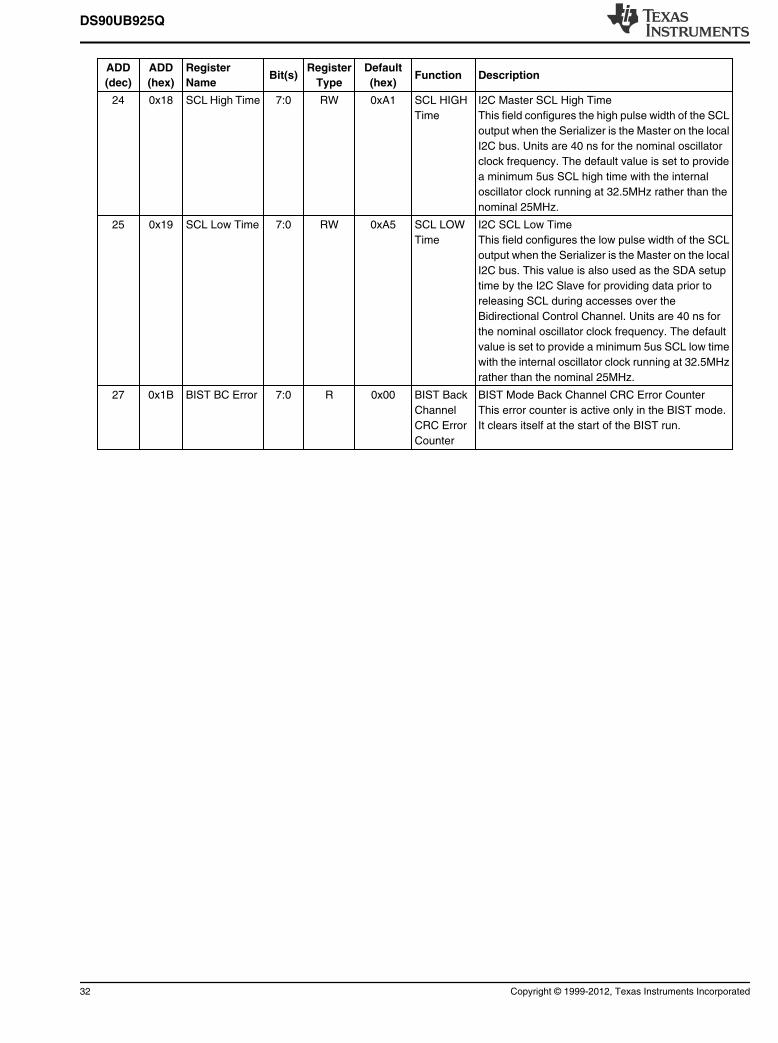
24 0x18 SCL High Time 7:0 RW 0xA1 SCL HIGH
Time
I2C Master SCL High Time
This field configures the high pulse width of the SCL
output when the Serializer is the Master on the local
I2C bus. Units are 40 ns for the nominal oscillator
clock frequency. The default value is set to provide
a minimum 5us SCL high time with the internal
oscillator clock running at 32.5MHz rather than the
nominal 25MHz.
25 0x19 SCL Low Time 7:0 RW 0xA5 SCL LOW
Time
I2C SCL Low Time
This field configures the low pulse width of the SCL
output when the Serializer is the Master on the local
I2C bus. This value is also used as the SDA setup
time by the I2C Slave for providing data prior to
releasing SCL during accesses over the
Bidirectional Control Channel. Units are 40 ns for
the nominal oscillator clock frequency. The default
value is set to provide a minimum 5us SCL low time
with the internal oscillator clock running at 32.5MHz
rather than the nominal 25MHz.
27 0x1B BIST BC Error 7:0 R 0x00 BIST Back
Channel
CRC Error
Counter
BIST Mode Back Channel CRC Error Counter
This error counter is active only in the BIST mode.
It clears itself at the start of the BIST run.
DS90UB925Q
32 Copyright © 1999-2012, Texas Instruments Incorporated
ADD
(dec)
ADD
(hex)
Register
NameBit(s)
Register
Type
Default
(hex)Function Description
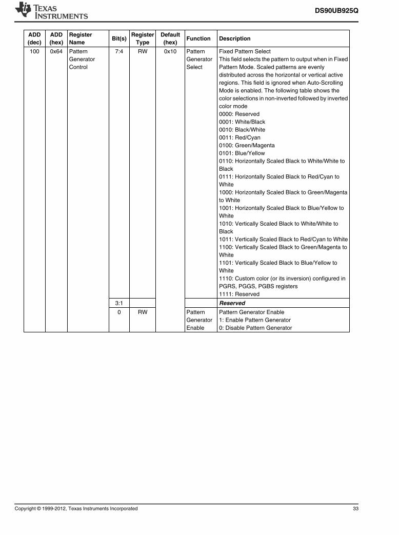
100 0x64 Pattern
Generator
Control
7:4 RW 0x10 Pattern
Generator
Select
Fixed Pattern Select
This field selects the pattern to output when in Fixed
Pattern Mode. Scaled patterns are evenly
distributed across the horizontal or vertical active
regions. This field is ignored when Auto-Scrolling
Mode is enabled. The following table shows the
color selections in non-inverted followed by inverted
color mode
0000: Reserved
0001: White/Black
0010: Black/White
0011: Red/Cyan
0100: Green/Magenta
0101: Blue/Yellow
0110: Horizontally Scaled Black to White/White to
Black
0111: Horizontally Scaled Black to Red/Cyan to
White
1000: Horizontally Scaled Black to Green/Magenta
to White
1001: Horizontally Scaled Black to Blue/Yellow to
White
1010: Vertically Scaled Black to White/White to
Black
1011: Vertically Scaled Black to Red/Cyan to White
1100: Vertically Scaled Black to Green/Magenta to
White
1101: Vertically Scaled Black to Blue/Yellow to
White
1110: Custom color (or its inversion) configured in
PGRS, PGGS, PGBS registers
1111: Reserved
3:1 Reserved
0 RW Pattern
Generator
Enable
Pattern Generator Enable
1: Enable Pattern Generator
0: Disable Pattern Generator
DS90UB925Q
Copyright © 1999-2012, Texas Instruments Incorporated 33
ADD
(dec)
ADD
(hex)
Register
NameBit(s)
Register
Type
Default
(hex)Function Description
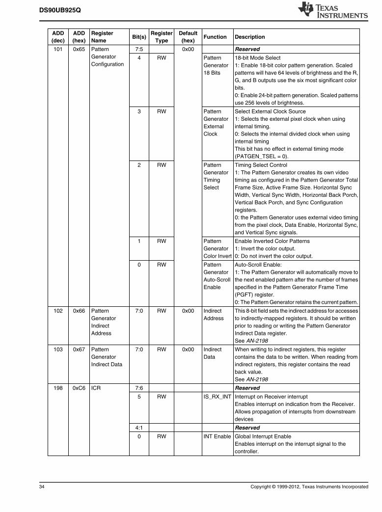
101 0x65 Pattern
Generator
Configuration
7:5 0x00 Reserved
4 RW Pattern
Generator
18 Bits
18-bit Mode Select
1: Enable 18-bit color pattern generation. Scaled
patterns will have 64 levels of brightness and the R,
G, and B outputs use the six most significant color
bits.
0: Enable 24-bit pattern generation. Scaled patterns
use 256 levels of brightness.
3 RW Pattern
Generator
External
Clock
Select External Clock Source
1: Selects the external pixel clock when using
internal timing.
0: Selects the internal divided clock when using
internal timing
This bit has no effect in external timing mode
(PATGEN_TSEL = 0).
2 RW Pattern
Generator
Timing
Select
Timing Select Control
1: The Pattern Generator creates its own video
timing as configured in the Pattern Generator Total
Frame Size, Active Frame Size. Horizontal Sync
Width, Vertical Sync Width, Horizontal Back Porch,
Vertical Back Porch, and Sync Configuration
registers.
0: the Pattern Generator uses external video timing
from the pixel clock, Data Enable, Horizontal Sync,
and Vertical Sync signals.
1 RW Pattern
Generator
Color Invert
Enable Inverted Color Patterns
1: Invert the color output.
0: Do not invert the color output.
0 RW Pattern
Generator
Auto-Scroll
Enable
Auto-Scroll Enable:
1: The Pattern Generator will automatically move to
the next enabled pattern after the number of frames
specified in the Pattern Generator Frame Time
(PGFT) register.
0: The Pattern Generator retains the current pattern.
102 0x66 Pattern
Generator
Indirect
Address
7:0 RW 0x00 Indirect
Address
This 8-bit field sets the indirect address for accesses
to indirectly-mapped registers. It should be written
prior to reading or writing the Pattern Generator
Indirect Data register.
See AN-2198
103 0x67 Pattern
Generator
Indirect Data
7:0 RW 0x00 Indirect
Data
When writing to indirect registers, this register
contains the data to be written. When reading from
indirect registers, this register contains the read
back value.
See AN-2198
198 0xC6 ICR 7:6 Reserved
5 RW IS_RX_INT Interrupt on Receiver interrupt
Enables interrupt on indication from the Receiver.
Allows propagation of interrupts from downstream
devices
4:1 Reserved
0 RW INT Enable Global Interrupt Enable
Enables interrupt on the interrupt signal to the
controller.
DS90UB925Q
34 Copyright © 1999-2012, Texas Instruments Incorporated
ADD
(dec)
ADD
(hex)
Register
NameBit(s)
Register
Type
Default
(hex)Function Description
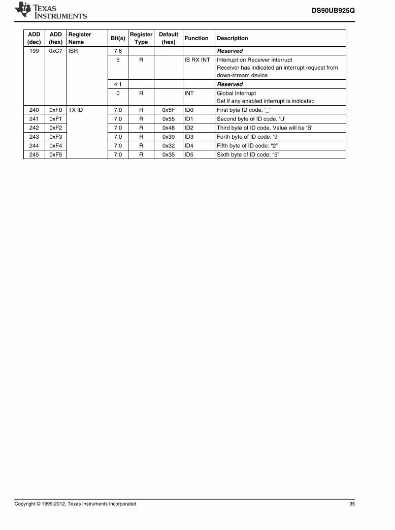
199 0xC7 ISR 7:6 Reserved
5 R IS RX INT Interrupt on Receiver interrupt
Receiver has indicated an interrupt request from
down-stream device
4:1 Reserved
0 R INT Global Interrupt
Set if any enabled interrupt is indicated
240 0xF0 TX ID 7:0 R 0x5F ID0 First byte ID code, ‘_’
241 0xF1 7:0 R 0x55 ID1 Second byte of ID code, ‘U’
242 0xF2 7:0 R 0x48 ID2 Third byte of ID code. Value will be ‘B’
243 0xF3 7:0 R 0x39 ID3 Forth byte of ID code: ‘9’
244 0xF4 7:0 R 0x32 ID4 Fifth byte of ID code: “2”
245 0xF5 7:0 R 0x35 ID5 Sixth byte of ID code: “5”
DS90UB925Q
Copyright © 1999-2012, Texas Instruments Incorporated 35
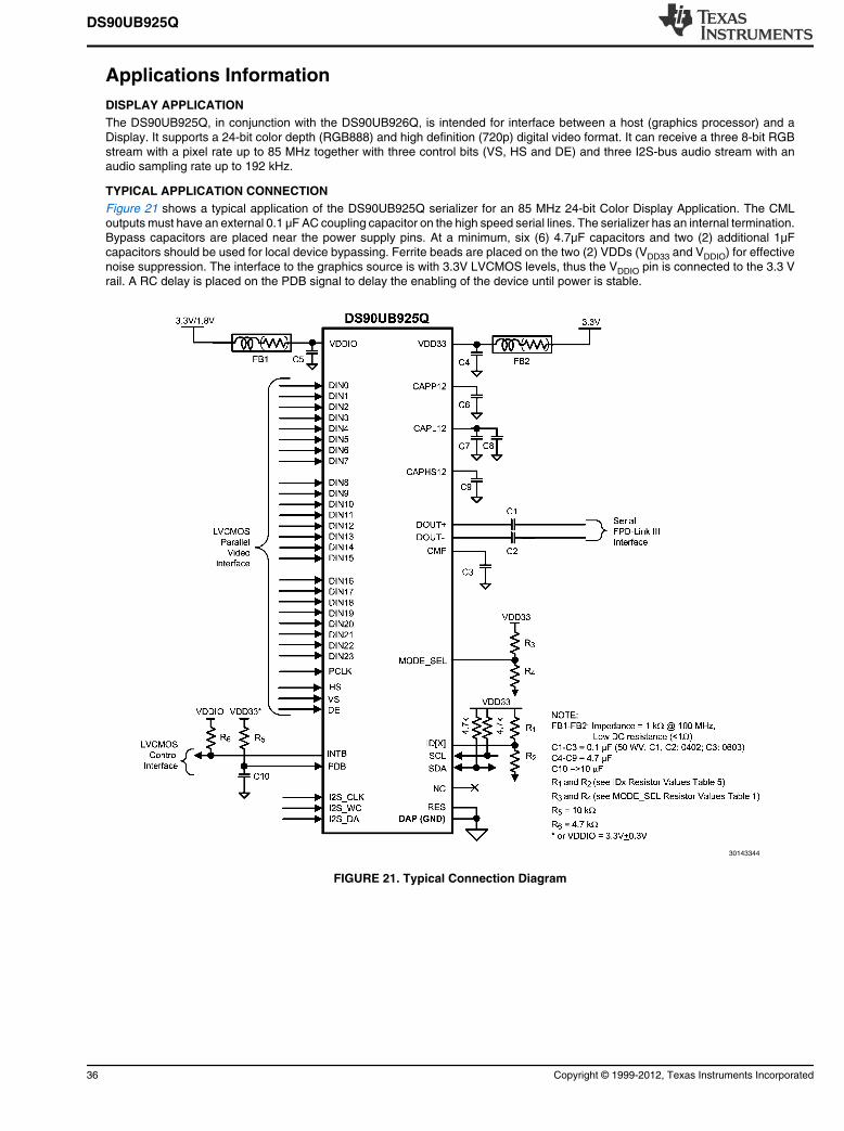
Applications Information
DISPLAY APPLICATION
The DS90UB925Q, in conjunction with the DS90UB926Q, is intended for interface between a host (graphics processor) and aDisplay. It supports a 24-bit color depth (RGB888) and high definition (720p) digital video format. It can receive a three 8-bit RGBstream with a pixel rate up to 85 MHz together with three control bits (VS, HS and DE) and three I2S-bus audio stream with anaudio sampling rate up to 192 kHz.
TYPICAL APPLICATION CONNECTION
Figure 21 shows a typical application of the DS90UB925Q serializer for an 85 MHz 24-bit Color Display Application. The CMLoutputs must have an external 0.1 μF AC coupling capacitor on the high speed serial lines. The serializer has an internal termination.Bypass capacitors are placed near the power supply pins. At a minimum, six (6) 4.7μF capacitors and two (2) additional 1μFcapacitors should be used for local device bypassing. Ferrite beads are placed on the two (2) VDDs (VDD33 and VDDIO) for effectivenoise suppression. The interface to the graphics source is with 3.3V LVCMOS levels, thus the VDDIO pin is connected to the 3.3 Vrail. A RC delay is placed on the PDB signal to delay the enabling of the device until power is stable.
30143344
FIGURE 21. Typical Connection Diagram
DS90UB925Q
36 Copyright © 1999-2012, Texas Instruments Incorporated
POWER UP REQUIREMENTS AND PDB PIN
The VDDs (VDD33 and VDDIO) supply ramp should be faster than 1.5 ms with a monotonic rise. A large capacitor on the PDB pin isneeded to ensure PDB arrives after all the VDDs have settled to the recommended operating voltage. When PDB pin is pulled toVDDIO = 3.0V to 3.6V or VDD33, it is recommended to use a 10 kΩ pull-up and a >10 uF cap to GND to delay the PDB input signal.
All inputs must not be driven until VDD33 and VDDIO has reached its steady state value.
PCB LAYOUT AND POWER SYSTEM CONSIDERATIONS
Circuit board layout and stack-up for the FPD-Link III devices should be designed to provide low-noise power feed to the device.Good layout practice will also separate high frequency or high-level inputs and outputs to minimize unwanted stray noise pickup,feedback and interference. Power system performance may be greatly improved by using thin dielectrics (2 to 4 mils) for power /ground sandwiches. This arrangement provides plane capacitance for the PCB power system with low-inductance parasitics, whichhas proven especially effective at high frequencies, and makes the value and placement of external bypass capacitors less critical.External bypass capacitors should include both RF ceramic and tantalum electrolytic types. RF capacitors may use values in therange of 0.01 uF to 0.1 uF. Tantalum capacitors may be in the 2.2 uF to 10 uF range. Voltage rating of the tantalum capacitorsshould be at least 5X the power supply voltage being used.
Surface mount capacitors are recommended due to their smaller parasitics. When using multiple capacitors per supply pin, locatethe smaller value closer to the pin. A large bulk capacitor is recommend at the point of power entry. This is typically in the 50uF to100uF range and will smooth low frequency switching noise. It is recommended to connect power and ground pins directly to thepower and ground planes with bypass capacitors connected to the plane with via on both ends of the capacitor. Connecting poweror ground pins to an external bypass capacitor will increase the inductance of the path.
A small body size X7R chip capacitor, such as 0603 or 0402, is recommended for external bypass. Its small body size reduces theparasitic inductance of the capacitor. The user must pay attention to the resonance frequency of these external bypass capacitors,usually in the range of 20-30 MHz. To provide effective bypassing, multiple capacitors are often used to achieve low impedancebetween the supply rails over the frequency of interest. At high frequency, it is also a common practice to use two vias from powerand ground pins to the planes, reducing the impedance at high frequency.
Some devices provide separate power and ground pins for different portions of the circuit. This is done to isolate switching noiseeffects between different sections of the circuit. Separate planes on the PCB are typically not required. Pin Description tablestypically provide guidance on which circuit blocks are connected to which power pin pairs. In some cases, an external filter may beused to provide clean power to sensitive circuits such as PLLs.
Use at least a four layer board with a power and ground plane. Locate LVCMOS signals away from the CML lines to prevent couplingfrom the LVCMOS lines to the CML lines. Closely-coupled differential lines of 100 Ohms are typically recommended for CMLinterconnect. The closely coupled lines help to ensure that coupled noise will appear as common-mode and thus is rejected by thereceivers. The tightly coupled lines will also radiate less.
Information on the LLP style package is provided in TI Application Note: AN-1187.
CML INTERCONNECT GUIDELINES
See AN-1108 and AN-905 for full details.
• Use 100Ω coupled differential pairs
• Use the S/2S/3S rule in spacings– S = space between the pair– 2S = space between pairs– 3S = space to LVCMOS signal
• Minimize the number of Vias
• Use differential connectors when operating above 500 Mbps line speed
• Maintain balance of the traces
• Minimize skew within the pair
Additional general guidance can be found in the LVDS Owner’s Manual - available in PDF format from the Texas Instruments website at: www.ti.com/lvds
DS90UB925Q
Copyright © 1999-2012, Texas Instruments Incorporated 37
Revision
• March 30, 2012
— Web release
• July 19, 2012
— Converted to hybrid TI format
— Corrected typo in “Pin Descriptions” SCL from pin 6 to pin 8
— Corrected typo in “Pin Descriptions” SDA from pin 7 to pin 9
— Corrected typo in “TABLE 1. Configuration Select (MODE_SEL)“ #6 ”I2S Channel B (18–bit Mode)“ from L to H
— Corrected typo in TABLE 5. Serial Control Bus Addresses for IDx #11 Ideal VR2(V) from 2.475 to 1.475
— Added “Note: BIST is not available in backwards compatible mode.”
— Corrected typo in table “DC and AC Serial Control Bus Characteristics” from VDDIO to VDD33
DS90UB925Q
38 Copyright © 1999-2012, Texas Instruments Incorporated
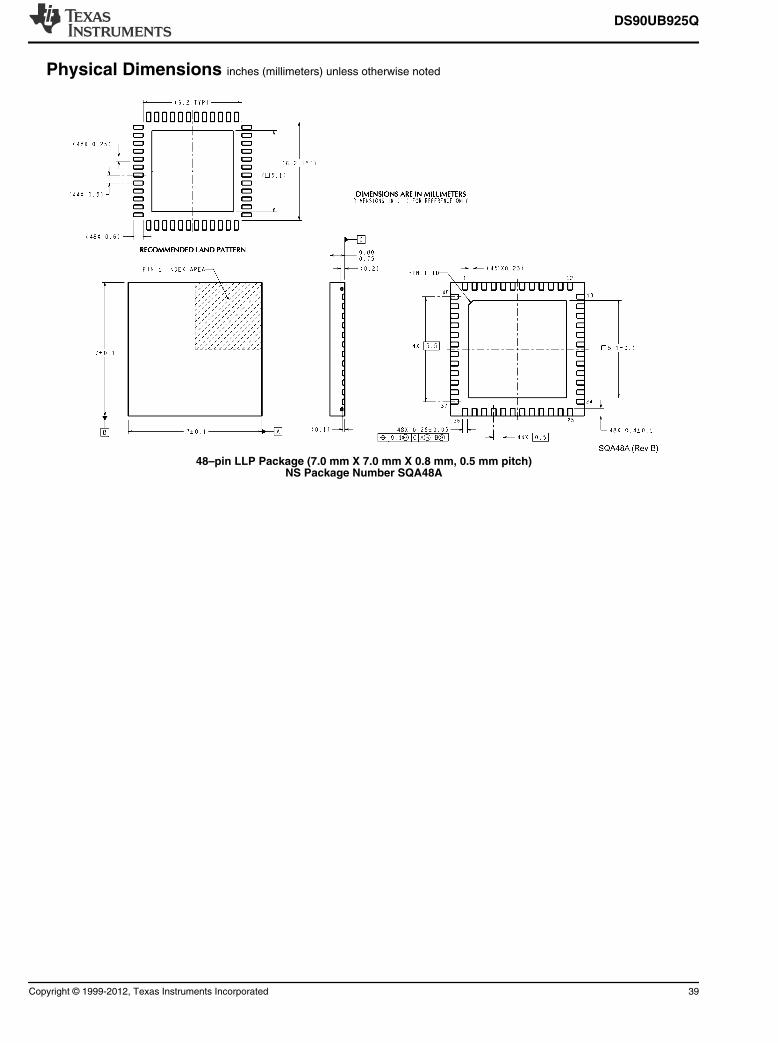
Physical Dimensions inches (millimeters) unless otherwise noted
48–pin LLP Package (7.0 mm X 7.0 mm X 0.8 mm, 0.5 mm pitch)NS Package Number SQA48A
DS90UB925Q
Copyright © 1999-2012, Texas Instruments Incorporated 39

Notes
Copyright © 1999-2012, Texas InstrumentsIncorporated
IMPORTANT NOTICE
Texas Instruments Incorporated and its subsidiaries (TI) reserve the right to make corrections, enhancements, improvements and otherchanges to its semiconductor products and services per JESD46C and to discontinue any product or service per JESD48B. Buyers shouldobtain the latest relevant information before placing orders and should verify that such information is current and complete. Allsemiconductor products (also referred to herein as “components”) are sold subject to TI’s terms and conditions of sale supplied at the timeof order acknowledgment.
TI warrants performance of its components to the specifications applicable at the time of sale, in accordance with the warranty in TI’s termsand conditions of sale of semiconductor products. Testing and other quality control techniques are used to the extent TI deems necessaryto support this warranty. Except where mandated by applicable law, testing of all parameters of each component is not necessarilyperformed.
TI assumes no liability for applications assistance or the design of Buyers’ products. Buyers are responsible for their products andapplications using TI components. To minimize the risks associated with Buyers’ products and applications, Buyers should provideadequate design and operating safeguards.
TI does not warrant or represent that any license, either express or implied, is granted under any patent right, copyright, mask work right, orother intellectual property right relating to any combination, machine, or process in which TI components or services are used. Informationpublished by TI regarding third-party products or services does not constitute a license to use such products or services or a warranty orendorsement thereof. Use of such information may require a license from a third party under the patents or other intellectual property of thethird party, or a license from TI under the patents or other intellectual property of TI.
Reproduction of significant portions of TI information in TI data books or data sheets is permissible only if reproduction is without alterationand is accompanied by all associated warranties, conditions, limitations, and notices. TI is not responsible or liable for such altereddocumentation. Information of third parties may be subject to additional restrictions.
Resale of TI components or services with statements different from or beyond the parameters stated by TI for that component or servicevoids all express and any implied warranties for the associated TI component or service and is an unfair and deceptive business practice.TI is not responsible or liable for any such statements.
Buyer acknowledges and agrees that it is solely responsible for compliance with all legal, regulatory and safety-related requirementsconcerning its products, and any use of TI components in its applications, notwithstanding any applications-related information or supportthat may be provided by TI. Buyer represents and agrees that it has all the necessary expertise to create and implement safeguards whichanticipate dangerous consequences of failures, monitor failures and their consequences, lessen the likelihood of failures that might causeharm and take appropriate remedial actions. Buyer will fully indemnify TI and its representatives against any damages arising out of the useof any TI components in safety-critical applications.
In some cases, TI components may be promoted specifically to facilitate safety-related applications. With such components, TI’s goal is tohelp enable customers to design and create their own end-product solutions that meet applicable functional safety standards andrequirements. Nonetheless, such components are subject to these terms.
No TI components are authorized for use in FDA Class III (or similar life-critical medical equipment) unless authorized officers of the partieshave executed a special agreement specifically governing such use.
Only those TI components which TI has specifically designated as military grade or “enhanced plastic” are designed and intended for use inmilitary/aerospace applications or environments. Buyer acknowledges and agrees that any military or aerospace use of TI componentswhich have not been so designated is solely at the Buyer's risk, and that Buyer is solely responsible for compliance with all legal andregulatory requirements in connection with such use.
TI has specifically designated certain components which meet ISO/TS16949 requirements, mainly for automotive use. Components whichhave not been so designated are neither designed nor intended for automotive use; and TI will not be responsible for any failure of suchcomponents to meet such requirements.
Products Applications
Audio www.ti.com/audio Automotive and Transportation www.ti.com/automotive
Amplifiers amplifier.ti.com Communications and Telecom www.ti.com/communications
Data Converters dataconverter.ti.com Computers and Peripherals www.ti.com/computers
DLP® Products www.dlp.com Consumer Electronics www.ti.com/consumer-apps
DSP dsp.ti.com Energy and Lighting www.ti.com/energy
Clocks and Timers www.ti.com/clocks Industrial www.ti.com/industrial
Interface interface.ti.com Medical www.ti.com/medical
Logic logic.ti.com Security www.ti.com/security
Power Mgmt power.ti.com Space, Avionics and Defense www.ti.com/space-avionics-defense
Microcontrollers microcontroller.ti.com Video and Imaging www.ti.com/video
RFID www.ti-rfid.com
OMAP Mobile Processors www.ti.com/omap TI E2E Community e2e.ti.com
Wireless Connectivity www.ti.com/wirelessconnectivity
Mailing Address: Texas Instruments, Post Office Box 655303, Dallas, Texas 75265Copyright © 2012, Texas Instruments Incorporated


![U2751A USB Modular Switch Matrix–Data Sheet...– LO-Earth 55 pF 35 pF 85 pF 45 pF Crosstalk at terminal block (ch-ch)[3] – 300 kHz – 1 MHz – 20 MHz – 45 MHz –70 dB –60](https://img.pdfslide.us/doc/110x75/5f099c707e708231d427a977/u2751a-usb-modular-switch-matrixadata-sheet-a-lo-earth-55-pf-35-pf-85-pf.jpg)


![[XLS]navy-training-transformation2.wikispaces.com · Web view0. 15 15. 85 85. 100 100. 5. 85. 100. 0.3 1 0.35 0.35 1. 85 85 85 85. 85 85 85 85. 85 85 85 85. 85 85 85 85. 85 85 85](https://img.pdfslide.us/doc/110x75/5b3ecf5e7f8b9a5e2c8b55c9/xlsnavy-training-web-view0-15-15-85-85-100-100-5-85-100-03-1-035.jpg)


![arXiv:2005.13949v1 [physics.app-ph] 25 May 20207.5 MHz F4 6.5 MHz F5 F6 7.5 MHz F7 F8 6.5 MHz F14 9.5 MHz F15 NA F16 8.5 MHz F17 NA F18 NA F19 7.5 MHz F11 6.5 MHz F20 NA F21 8.5 MHz](https://img.pdfslide.us/doc/110x75/5f758878eb2d114487007824/arxiv200513949v1-25-may-2020-75-mhz-f4-65-mhz-f5-f6-75-mhz-f7-f8-65-mhz.jpg)


![[XLS]navy-training-transformation2.wikispaces.com · Web view0 15 15 85 85 100 100 5 85 100 0.3 1 0.35 0.35 1 85 85 85 85 85 85 85 85 85 85 85 85 85 85 85 85 85 85 85 85 15 15 5 11.5](https://img.pdfslide.us/doc/110x75/5adf226a7f8b9a6e5c8bbbe3/xlsnavy-training-view0-15-15-85-85-100-100-5-85-100-03-1-035-035-1-85-85-85.jpg)