Embed Size (px)
Citation preview
Copyright (c) 2013 IEEE. Personal use is permitted. For any other purposes, permission must be obtained from the IEEE by emailing [email protected].
This article has been accepted for publication in a future issue of this journal, but has not been fully edited. Content may change prior to final publication.
JSTQE-INV-NB-04992-2013 1
Abstract— Surface enhanced Raman scattering (SERS) is
undergoing a renaissance, spurred largely by developments in the burgeoning field of plasmonics. This paper reviews the current status and future directions in plasmonic nanostructures for SERS. We show that engineered plasmonic nanostructures enable exciting new functionalities, including beamed Raman scattering and highly reproducible chips for single molecule SERS. We furthermore show that silicon photonics enables SERS to be performed using optically-trapped Ag nanoparticle clusters.
Index Terms— Chemical and biological sensors, nanofabrication, nanolithography, nanomaterials, nanophotonics, nanoscale devices, Raman scattering, surface plasmons (SPs).
I. INTRODUCTION ECENT years have seen an explosion of interest in the field of plasmonics, which has come to refer to the use of
surface plasmon polaritons (SPPs) to route and manipulate light on the nanoscale [1]. An exciting range of applications have been enabled that are too diverse to fully review here, but include highly miniaturized optical devices, such as lasers [2, 3], waveguides [4], photodetectors [5] and modulators [6], biosensors [7], heat-assisted magnetic recording [8], polarization elements [9-11], optical tweezers [12-18] and metamaterials [19]. We argue, however, that one of the most
Manuscript received August 13, 2013; revised September 8, 2013. First published ZZ; current version published AA. This work was supported by the National Science Foundation (NSF, grant ECCS-0747560 and grant ECCS-1201687), the Harvard Quantum Optics Center, and by the Center for Excitonics, an Energy Frontier Research Center funded by the U.S. Department of Energy, Office of Science and Office of Basic Energy Sciences under Award Number DE-SC0001088. This work was also supported by the UT/ORNL Joint Institute for Advanced Materials, and the U.S. Department of Energy, Office of Basic Energy Sciences, under Award Number DESC0004792 (J.P.C.) and the National Science Foundation under Awards CHE-0954297 and DMR-0906752 (M.D.B.). Fabrication work was carried out in the Harvard Center for Nanoscale Systems, which is supported by the NSF.
Wenqi Zhu, Dongxing Wang, and Kenneth B. Crozier are with the School of Engineering and Applied Sciences, Harvard University, Cambridge, MA 02138 USA (emails: [email protected], [email protected], and [email protected]).
Shiyun Lin was with the School of Engineering and Applied Sciences, Harvard University, Cambridge, MA 02138 USA. He is now with Oracle (email: [email protected]).
Michael D. Best and Jon P. Camden are with the Department of Chemistry, University of Tennessee, Knoxville, TN 37996, USA (emails: [email protected] and [email protected]).
compelling applications for plasmonics is surface enhanced Raman scattering (SERS). While the SERS phenomenon was reported some time ago [20, 21], the recent upsurge in plasmonics has enabled exciting new capabilities. In this paper, we first review the SERS phenomenon. We then outline how plasmonics and nanophotonics have enabled beamed Raman scattering, single molecule SERS on a chip, and SERS with metal nanoparticles optically trapped by photonic resonators. These advances have been in part enabled by thinking about the plasmon structures as antennas [22-26]. To understand SERS, we begin by considering the Raman process [27]. When light is scattered by a molecule (Fig. 1), the process is generally elastic, a process is termed Rayleigh scattering. This can be modeled classically by considering the molecule to act as a dipole 𝑝 that oscillates at the same frequency 𝜈𝐿 as the incident electric field 𝐸�⃗ , with 𝑝 = 𝛼�𝐿 ∙ 𝐸�⃗ where 𝛼�𝐿 is the linear polarizability tensor. On the other hand, a molecule containing 𝑁 atoms (𝑁 ≥ 2) will have 3𝑁 − 6 vibrational modes (3𝑁 − 5 for linear molecules). Each corresponds to a particular vibrational pattern, in which the atoms of the molecule oscillate at frequency 𝜈𝑀, with 𝑄𝑘 measuring the oscillation amplitude and termed the normal mode coordinate. These perturbations modify the molecule’s polarizability. This can be expressed as follows:
𝛼�𝐿(𝑄𝑘) = 𝛼�𝐿(0) + �𝜕𝛼�𝐿𝜕𝑄𝑘
�𝑄𝑘=0
𝑄𝑘 + 12�𝜕
2𝛼�𝐿𝜕𝑄𝑘
2 �𝑄𝑘=0
𝑄𝑘2 + ⋯ (1)
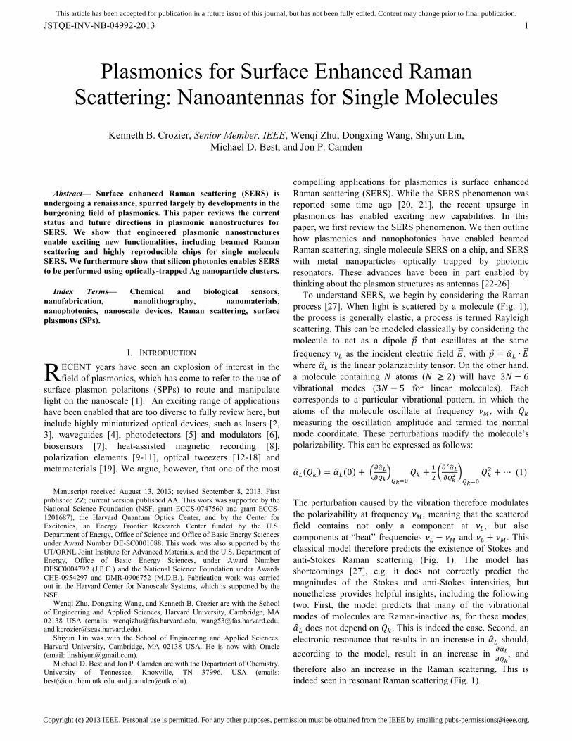
The perturbation caused by the vibration therefore modulates the polarizability at frequency 𝜈𝑀, meaning that the scattered field contains not only a component at 𝜈𝐿 , but also components at “beat” frequencies 𝜈𝐿 − 𝜈𝑀 and 𝜈𝐿 + 𝜈𝑀. This classical model therefore predicts the existence of Stokes and anti-Stokes Raman scattering (Fig. 1). The model has shortcomings [27], e.g. it does not correctly predict the magnitudes of the Stokes and anti-Stokes intensities, but nonetheless provides helpful insights, including the following two. First, the model predicts that many of the vibrational modes of molecules are Raman-inactive as, for these modes, 𝛼�𝐿 does not depend on 𝑄𝑘. This is indeed the case. Second, an electronic resonance that results in an increase in 𝛼�𝐿 should, according to the model, result in an increase in 𝜕𝛼�𝐿
𝜕𝑄𝑘, and
therefore also an increase in the Raman scattering. This is indeed seen in resonant Raman scattering (Fig. 1).
Plasmonics for Surface Enhanced Raman Scattering: Nanoantennas for Single Molecules
Kenneth B. Crozier, Senior Member, IEEE, Wenqi Zhu, Dongxing Wang, Shiyun Lin, Michael D. Best, and Jon P. Camden
R
Copyright (c) 2013 IEEE. Personal use is permitted. For any other purposes, permission must be obtained from the IEEE by emailing [email protected].
This article has been accepted for publication in a future issue of this journal, but has not been fully edited. Content may change prior to final publication.
JSTQE-INV-NB-04992-2013 2
Fig. 1. Elastic (Rayleigh) and inelastic (Raman) scattering
of light by a molecule (here taken as benzenethiol). Raman spectroscopy is a powerful technique as it enables
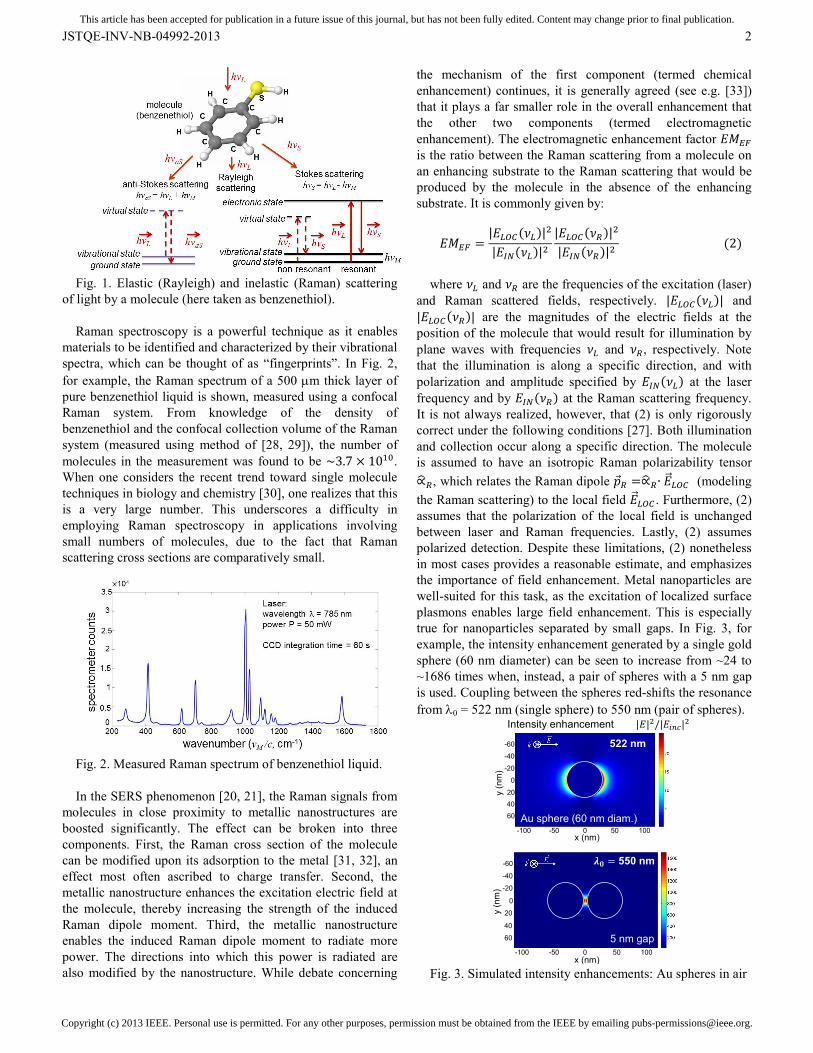
materials to be identified and characterized by their vibrational spectra, which can be thought of as “fingerprints”. In Fig. 2, for example, the Raman spectrum of a 500 µm thick layer of pure benzenethiol liquid is shown, measured using a confocal Raman system. From knowledge of the density of benzenethiol and the confocal collection volume of the Raman system (measured using method of [28, 29]), the number of molecules in the measurement was found to be ~3.7 × 10¹⁰. When one considers the recent trend toward single molecule techniques in biology and chemistry [30], one realizes that this is a very large number. This underscores a difficulty in employing Raman spectroscopy in applications involving small numbers of molecules, due to the fact that Raman scattering cross sections are comparatively small.
Fig. 2. Measured Raman spectrum of benzenethiol liquid. In the SERS phenomenon [20, 21], the Raman signals from
molecules in close proximity to metallic nanostructures are boosted significantly. The effect can be broken into three components. First, the Raman cross section of the molecule can be modified upon its adsorption to the metal [31, 32], an effect most often ascribed to charge transfer. Second, the metallic nanostructure enhances the excitation electric field at the molecule, thereby increasing the strength of the induced Raman dipole moment. Third, the metallic nanostructure enables the induced Raman dipole moment to radiate more power. The directions into which this power is radiated are also modified by the nanostructure. While debate concerning
the mechanism of the first component (termed chemical enhancement) continues, it is generally agreed (see e.g. [33]) that it plays a far smaller role in the overall enhancement that the other two components (termed electromagnetic enhancement). The electromagnetic enhancement factor 𝐸𝑀𝐸𝐹 is the ratio between the Raman scattering from a molecule on an enhancing substrate to the Raman scattering that would be produced by the molecule in the absence of the enhancing substrate. It is commonly given by:
𝐸𝑀𝐸𝐹 =|𝐸𝐿𝑂𝐶(𝜈𝐿)|2
|𝐸𝐼𝑁(𝜈𝐿)|2|𝐸𝐿𝑂𝐶(𝜈𝑅)|2
|𝐸𝐼𝑁(𝜈𝑅)|2 (2)
where 𝜈𝐿 and 𝜈𝑅 are the frequencies of the excitation (laser)
and Raman scattered fields, respectively. |𝐸𝐿𝑂𝐶(𝜈𝐿)| and |𝐸𝐿𝑂𝐶(𝜈𝑅)| are the magnitudes of the electric fields at the position of the molecule that would result for illumination by plane waves with frequencies 𝜈𝐿 and 𝜈𝑅, respectively. Note that the illumination is along a specific direction, and with polarization and amplitude specified by 𝐸𝐼𝑁(𝜈𝐿) at the laser frequency and by 𝐸𝐼𝑁(𝜈𝑅) at the Raman scattering frequency. It is not always realized, however, that (2) is only rigorously correct under the following conditions [27]. Both illumination and collection occur along a specific direction. The molecule is assumed to have an isotropic Raman polarizability tensor ∝�𝑅, which relates the Raman dipole 𝑝𝑅 =∝�𝑅∙ 𝐸�⃗ 𝐿𝑂𝐶 (modeling the Raman scattering) to the local field 𝐸�⃗ 𝐿𝑂𝐶 . Furthermore, (2) assumes that the polarization of the local field is unchanged between laser and Raman frequencies. Lastly, (2) assumes polarized detection. Despite these limitations, (2) nonetheless in most cases provides a reasonable estimate, and emphasizes the importance of field enhancement. Metal nanoparticles are well-suited for this task, as the excitation of localized surface plasmons enables large field enhancement. This is especially true for nanoparticles separated by small gaps. In Fig. 3, for example, the intensity enhancement generated by a single gold sphere (60 nm diameter) can be seen to increase from ~24 to ~1686 times when, instead, a pair of spheres with a 5 nm gap is used. Coupling between the spheres red-shifts the resonance from λ0 = 522 nm (single sphere) to 550 nm (pair of spheres).
Fig. 3. Simulated intensity enhancements: Au spheres in air
Intensity enhancement
522 nm
550 nm
Au sphere (60 nm diam.)
5 nm gap-100 -50 0 50 100
60
40
20
0
-20
-40
-60
x (nm)
y (n
m)
-100 -50 0 50 100x (nm)
60
4020
0
-20
-40
-60
y (n
m)
Copyright (c) 2013 IEEE. Personal use is permitted. For any other purposes, permission must be obtained from the IEEE by emailing [email protected].
This article has been accepted for publication in a future issue of this journal, but has not been fully edited. Content may change prior to final publication.
JSTQE-INV-NB-04992-2013 3
II. BEAMED RAMAN SCATTERING USING OPTICAL NANOANTENNAS
As noted in the Introduction, one mechanism by which metallic nanoparticles generate large SERS electromagnetic enhancements is that they produce larger excitation fields, and hence larger Raman dipole moments 𝑝𝑅. The other mechanism concerns the fact that they enable more power to be extracted from these dipole moments, and because the radiated fields produced are more directional. The importance of directionality in the design of SERS substrates has become better appreciated in recent years, an effect sometimes called “beamed Raman scattering” [34-37] or “directional SERS (DERS)” [38]. Observation of the angular emission patterns of fluorescence from single molecules and quantum dots via the direct imaging of the back focal planes of high numerical aperture objective lenses has been well established [39]. The observation of Raman emission patterns is challenging, however, due to the fact that Raman scattering is comparatively weak, and often accompanied by a broad background continuum. Here, we describe work [40] that demonstrated, for the first time to the best of our knowledge, the direct observation of beamed Raman scattering.
A. Emission from dimer nanoantennas Because pairs of metallic nanoparticles (“dimers”)
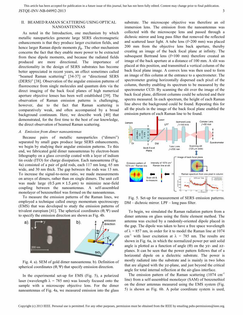
separated by small gaps produce large SERS enhancements, we begin by studying their angular emission patterns. To this end, we fabricated gold dimer nanoantennas by electron-beam lithography on a glass coverslip coated with a layer of indium tin oxide (ITO) for charge dissipation. Each nanoantenna (Fig. 4a) consisted of a pair of gold rods, each 117 nm long, 65 nm wide, and 30 nm thick. The gap between the rods was 13 nm. To increase the signal-to-noise ratio, we made measurements on arrays of dimers, rather than on single dimers. The unit cell was made large (0.5 𝜇𝑚 × 1.5 𝜇𝑚) to minimize near-field coupling between the nanoantennas. A self-assembled monolayer of benzenethiol was formed on the nanoantennas. To measure the emission patterns of the Raman lines, we employed a technique called energy momentum spectroscopy (EMS) that was developed to study the emission patterns of trivalent europium [41]. The spherical coordinates (Θ,Ψ) used to specify the emission direction are shown as Fig. 4b.
Fig. 4. a). SEM of gold dimer nanoantenna. b). Definition of
spherical coordinates (Θ,Ψ) that specify emission direction.
In the experimental set-up for EMS (Fig. 5), a polarized laser (wavelength λ = 785 nm) was loosely focused onto the sample with a microscope objective lens. For the dimer nanoantennas of Fig. 4a, we measured emission into the glass
substrate. The microscope objective was therefore an oil immersion lens. The emission from the nanoantennas was collected with the microscope lens and passed through a dichroic mirror and long pass filter that removed the reflected and scattered laser light. A tube lens (f=200 mm) was placed 200 mm from the objective lens back aperture, thereby creating an image of the back focal plane at infinity. The subsequent Bertrand lens (f=100 mm) therefore created an image of the back aperture at a distance of 100 mm. A slit was placed at this position, and transmitted a vertical column of the back focal plane image. A convex lens was then used to form an image of this column at the entrance to a spectrometer. The spectrometer grating horizontally dispersed each pixel of the column, thereby enabling its spectrum to be measured by the spectrometer CCD. By scanning the slit over the image of the back focal plane, different columns could be selected and their spectra measured. In each spectrum, the height of each Raman line above the background could be found. Repeating this for all the pixels in the image of the back focal plane enabled the emission pattern of each Raman line to be found.
Fig. 5. Set-up for measurement of SERS emission patterns. DM – dichroic mirror. LPF – long pass filter.
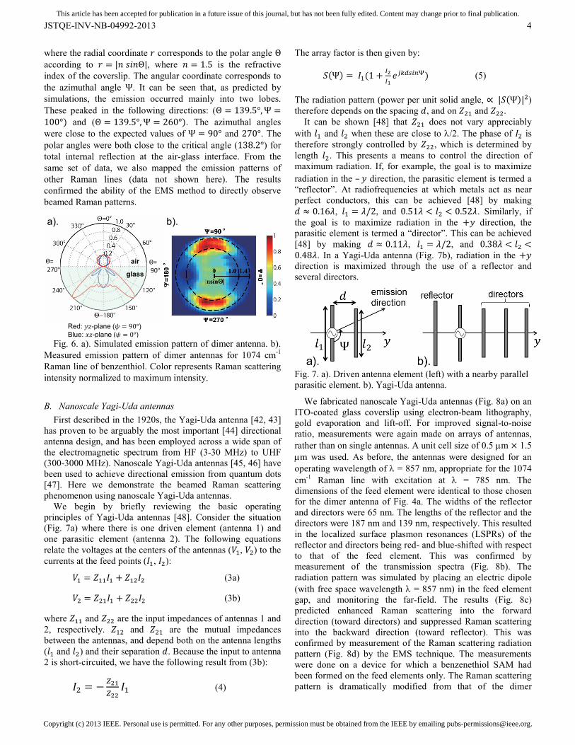
To begin, we simulated the Raman radiation pattern from a dimer antenna on glass using the finite element method. The antenna was excited by a randomly-oriented dipole placed in the gap. The dipole was taken to have a free space wavelength of λ = 857 nm, in order for it to model the Raman line at 1074 cm-1 with laser excitation at λ = 785 nm. The results are shown in Fig. 6a, in which the normalized power per unit solid angle is plotted as a function of angle (Θ) on the 𝑦𝑧- and 𝑥𝑧-planes. It can be seen that the power pattern follows that of a horizontal dipole on a dielectric substrate. The power is mostly radiated into the substrate and is mainly in two lobes that are aligned with the 𝑦𝑧-plane, and just beyond the critical angle for total internal reflection at the air-glass interface.
The emission pattern of the Raman scattering (1074 cm-1 line) from a self-assembled monolayer (SAM) of benzenethiol on the dimer antennas measured using the EMS system (Fig. 5) is shown as Fig. 6b. A polar coordinate system is used,
Image of back focal plane
Raman spectrum from one pixel in column
1074 cm-1 line
Intensity of 1074 cm-1
Raman line at slit
Scan slit &re-measure
Emission pattern of 1074 cm-1 Raman line
Scanning slit (120 µm wide)
Copyright (c) 2013 IEEE. Personal use is permitted. For any other purposes, permission must be obtained from the IEEE by emailing [email protected].
This article has been accepted for publication in a future issue of this journal, but has not been fully edited. Content may change prior to final publication.
JSTQE-INV-NB-04992-2013 4
where the radial coordinate 𝑟 corresponds to the polar angle Θ according to 𝑟 = |𝑛 𝑠𝑖𝑛Θ|, where 𝑛 = 1.5 is the refractive index of the coverslip. The angular coordinate corresponds to the azimuthal angle Ψ. It can be seen that, as predicted by simulations, the emission occurred mainly into two lobes. These peaked in the following directions: (Θ = 139.5°,Ψ =100°) and (Θ = 139.5°,Ψ = 260°). The azimuthal angles were close to the expected values of Ψ = 90° and 270°. The polar angles were both close to the critical angle (138.2°) for total internal reflection at the air-glass interface. From the same set of data, we also mapped the emission patterns of other Raman lines (data not shown here). The results confirmed the ability of the EMS method to directly observe beamed Raman patterns.
Fig. 6. a). Simulated emission pattern of dimer antenna. b).
Measured emission pattern of dimer antennas for 1074 cm-1 Raman line of benzenthiol. Color represents Raman scattering intensity normalized to maximum intensity.
B. Nanoscale Yagi-Uda antennas First described in the 1920s, the Yagi-Uda antenna [42, 43]
has proven to be arguably the most important [44] directional antenna design, and has been employed across a wide span of the electromagnetic spectrum from HF (3-30 MHz) to UHF (300-3000 MHz). Nanoscale Yagi-Uda antennas [45, 46] have been used to achieve directional emission from quantum dots [47]. Here we demonstrate the beamed Raman scattering phenomenon using nanoscale Yagi-Uda antennas. We begin by briefly reviewing the basic operating principles of Yagi-Uda antennas [48]. Consider the situation (Fig. 7a) where there is one driven element (antenna 1) and one parasitic element (antenna 2). The following equations relate the voltages at the centers of the antennas (𝑉1, 𝑉2) to the currents at the feed points (𝐼1, 𝐼2):
𝑉1 = 𝑍11𝐼1 + 𝑍12𝐼2 (3a)
𝑉2 = 𝑍21𝐼1 + 𝑍22𝐼2 (3b)
where 𝑍11 and 𝑍22 are the input impedances of antennas 1 and 2, respectively. 𝑍12 and 𝑍21 are the mutual impedances between the antennas, and depend both on the antenna lengths (𝑙1 and 𝑙2) and their separation 𝑑. Because the input to antenna 2 is short-circuited, we have the following result from (3b):
𝐼2 = −𝑍21𝑍22
𝐼1 (4)
The array factor is then given by:
𝑆(Ψ) = 𝐼1(1 + 𝐼2𝐼1𝑒𝑗𝑘𝑑𝑠𝑖𝑛Ψ) (5)
The radiation pattern (power per unit solid angle, ∝ |𝑆(Ψ)|2) therefore depends on the spacing 𝑑, and on 𝑍21 and 𝑍22.
It can be shown [48] that 𝑍21 does not vary appreciably with 𝑙1 and 𝑙2 when these are close to λ/2. The phase of 𝐼2 is therefore strongly controlled by 𝑍22, which is determined by length 𝑙2. This presents a means to control the direction of maximum radiation. If, for example, the goal is to maximize radiation in the – 𝑦 direction, the parasitic element is termed a “reflector”. At radiofrequencies at which metals act as near perfect conductors, this can be achieved [48] by making 𝑑 ≈ 0.16𝜆, 𝑙1 = 𝜆/2, and 0.51𝜆 < 𝑙2 < 0.52𝜆. Similarly, if the goal is to maximize radiation in the +𝑦 direction, the parasitic element is termed a “director”. This can be achieved [48] by making 𝑑 ≈ 0.11𝜆, 𝑙1 = 𝜆/2, and 0.38𝜆 < 𝑙2 <0.48𝜆. In a Yagi-Uda antenna (Fig. 7b), radiation in the +𝑦 direction is maximized through the use of a reflector and several directors.
Fig. 7. a). Driven antenna element (left) with a nearby parallel parasitic element. b). Yagi-Uda antenna.
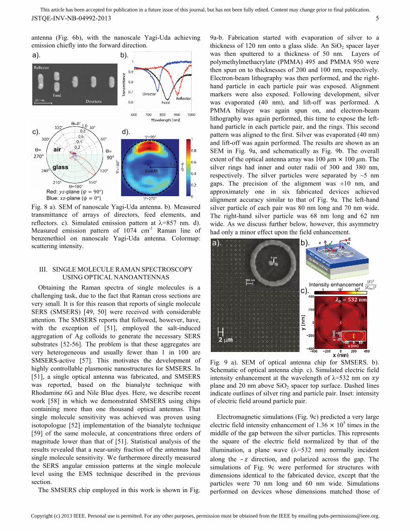
We fabricated nanoscale Yagi-Uda antennas (Fig. 8a) on an ITO-coated glass coverslip using electron-beam lithography, gold evaporation and lift-off. For improved signal-to-noise ratio, measurements were again made on arrays of antennas, rather than on single antennas. A unit cell size of 0.5 µm × 1.5 µm was used. As before, the antennas were designed for an operating wavelength of λ = 857 nm, appropriate for the 1074 cm-1 Raman line with excitation at λ = 785 nm. The dimensions of the feed element were identical to those chosen for the dimer antenna of Fig. 4a. The widths of the reflector and directors were 65 nm. The lengths of the reflector and the directors were 187 nm and 139 nm, respectively. This resulted in the localized surface plasmon resonances (LSPRs) of the reflector and directors being red- and blue-shifted with respect to that of the feed element. This was confirmed by measurement of the transmission spectra (Fig. 8b). The radiation pattern was simulated by placing an electric dipole (with free space wavelength λ = 857 nm) in the feed element gap, and monitoring the far-field. The results (Fig. 8c) predicted enhanced Raman scattering into the forward direction (toward directors) and suppressed Raman scattering into the backward direction (toward reflector). This was confirmed by measurement of the Raman scattering radiation pattern (Fig. 8d) by the EMS technique. The measurements were done on a device for which a benzenethiol SAM had been formed on the feed elements only. The Raman scattering pattern is dramatically modified from that of the dimer
glass
air
Red: 𝑦𝑧-plane (𝜓 = 90°)Blue: 𝑥𝑧-plane (𝜓 = 0°)
Θ=270°
Θ=90°
a). b).
Copyright (c) 2013 IEEE. Personal use is permitted. For any other purposes, permission must be obtained from the IEEE by emailing [email protected].
This article has been accepted for publication in a future issue of this journal, but has not been fully edited. Content may change prior to final publication.
JSTQE-INV-NB-04992-2013 5
antenna (Fig. 6b), with the nanoscale Yagi-Uda achieving emission chiefly into the forward direction.
Fig. 8 a). SEM of nanoscale Yagi-Uda antenna. b). Measured transmittance of arrays of directors, feed elements, and reflectors. c). Simulated emission pattern at λ=857 nm. d). Measured emission pattern of 1074 cm-1 Raman line of benzenethiol on nanoscale Yagi-Uda antenna. Colormap: scattering intensity.
III. SINGLE MOLECULE RAMAN SPECTROSCOPY USING OPTICAL NANOANTENNAS
Obtaining the Raman spectra of single molecules is a challenging task, due to the fact that Raman cross sections are very small. It is for this reason that reports of single molecule SERS (SMSERS) [49, 50] were received with considerable attention. The SMSERS reports that followed, however, have, with the exception of [51], employed the salt-induced aggregation of Ag colloids to generate the necessary SERS substrates [52-56]. The problem is that these aggregates are very heterogeneous and usually fewer than 1 in 100 are SMSERS-active [57]. This motivates the development of highly controllable plasmonic nanostructures for SMSERS. In [51], a single optical antenna was fabricated, and SMSERS was reported, based on the bianalyte technique with Rhodamine 6G and Nile Blue dyes. Here, we describe recent work [58] in which we demonstrated SMSERS using chips containing more than one thousand optical antennas. That single molecule sensitivity was achieved was proven using isotopologue [52] implementation of the bianalyte technique [59] of the same molecule, at concentrations three orders of magnitude lower than that of [51]. Statistical analysis of the results revealed that a near-unity fraction of the antennas had single molecule sensitivity. We furthermore directly measured the SERS angular emission patterns at the single molecule level using the EMS technique described in the previous section.
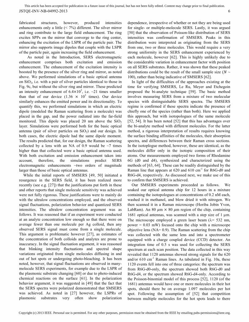
The SMSERS chip employed in this work is shown in Fig.
9a-b. Fabrication started with evaporation of silver to a thickness of 120 nm onto a glass slide. An SiO2 spacer layer was then sputtered to a thickness of 50 nm. Layers of polymethylmethacrylate (PMMA) 495 and PMMA 950 were then spun on to thicknesses of 200 and 100 nm, respectively. Electron-beam lithography was then performed, and the right-hand particle in each particle pair was exposed. Alignment markers were also exposed. Following development, silver was evaporated (40 nm), and lift-off was performed. A PMMA bilayer was again spun on, and electron-beam lithography was again performed, this time to expose the left-hand particle in each particle pair, and the rings. This second pattern was aligned to the first. Silver was evaporated (40 nm) and lift-off was again performed. The results are shown as an SEM in Fig. 9a, and schematically as Fig. 9b. The overall extent of the optical antenna array was 100 𝜇m × 100 𝜇m. The silver rings had inner and outer radii of 300 and 380 nm, respectively. The silver particles were separated by ~5 nm gaps. The precision of the alignment was ±10 nm, and approximately one in six fabricated devices achieved alignment accuracy similar to that of Fig. 9a. The left-hand silver particle of each pair was 80 nm long and 70 nm wide. The right-hand silver particle was 68 nm long and 62 nm wide. As we discuss further below, however, this asymmetry had only a minor effect upon the field enhancement.
Fig. 9 a). SEM of optical antenna chip for SMSERS. b). Schematic of optical antenna chip. c). Simulated electric field intensity enhancement at the wavelength of λ=532 nm on 𝑥𝑦 plane and 20 nm above SiO2 spacer top surface. Dashed lines indicate outlines of silver ring and particle pair. Inset: intensity of electric field around particle pair.
Electromagnetic simulations (Fig. 9c) predicted a very large
electric field intensity enhancement of 1.36 × 10⁵ times in the middle of the gap between the silver particles. This represents the square of the electric field normalized by that of the illumination, a plane wave (λ=532 nm) normally incident along the – 𝑧 direction, and polarized across the gap. The simulations of Fig. 9c were performed for structures with dimensions identical to the fabricated device, except that the particles were 70 nm long and 60 nm wide. Simulations performed on devices whose dimensions matched those of
glass
air Θ=90°
Θ=270°
a). b).
c). d).
Red: 𝑦𝑧-plane (𝜓 = 90°)Blue: 𝑥𝑧-plane (𝜓 = 0°)
𝝀𝟎 = 𝟓𝟑𝟐 𝒏𝒎
Intensity enhancement |𝐸|2
|𝐸𝑖𝑛𝑐|2
a). b).
c).
Copyright (c) 2013 IEEE. Personal use is permitted. For any other purposes, permission must be obtained from the IEEE by emailing [email protected].
This article has been accepted for publication in a future issue of this journal, but has not been fully edited. Content may change prior to final publication.
JSTQE-INV-NB-04992-2013 6
fabricated structures, however, produced intensities enhancements only a little (< 7%) different. The silver mirror and ring contribute to the large field enhancement. The ring excites SPPs on the mirror that converge to the ring center, enhancing the excitation of the LSPR of the particle pair. The mirror also supports image dipoles that couple with the LSPR of the particle pair, again increasing the field enhancement.
As noted in the Introduction, SERS electromagnetic enhancement comprises both excitation and emission enhancement. The enhancement of the excitation intensity is boosted by the presence of the silver ring and mirror, as noted above. We performed simulations of a basic optical antenna on SiO2, i.e. with a pair of silver particles identical to those in Fig. 9c, but without the silver ring and mirror. These predicted an intensity enhancement of 6.4×10³, i.e. ~21 times smaller than that of our device (1.36 × 10⁵ times). Our device similarly enhances the emitted power and its directionality. To quantify this, we performed simulations in which an electric dipole (modeled the Raman scattering from a molecule) was placed in the gap, and the power radiated into the far-field monitored. This dipole was placed 20 nm above the SiO2 layer. Simulations were performed both for the basic optical antenna (pair of silver particles on SiO2) and our design. In both cases, the electric dipole had the same dipole moment. The results predicted that, for our design, the Raman scattering collected by a lens with an NA of 0.9 would be ~7 times higher than that collected were a basic optical antenna used. With both excitation and emission enhancement taken into account, therefore, the simulations predict SERS electromagnetic enhancements ~two orders of magnitude larger than those of basic optical antennas.
While the initial reports of SMSERS [49, 50] initiated a resurgence in the SERS field, it has been realized more recently (see e.g. [27]) that the justifications put forth in these and other reports that single molecule sensitivity was achieved were not fully rigorous. These justifications were to mainly do with the ultralow concentrations employed, and the observed signal fluctuations, polarization behavior and quantized SERS intensities. The ultralow concentration argument was as follows. It was reasoned that if an experiment were conducted at an analyte concentration low enough so that there were on average fewer than one molecule per Ag colloid, then any observed SERS signal must come from a single molecule. This argument is problematic however [27], as estimates of the concentration of both colloids and analytes are prone to inaccuracy. In the signal fluctuation argument, it was reasoned that blinking intensity fluctuations and spectral shape variations originated from single molecules diffusing in and out of hot spots or undergoing photo-bleaching. It has been noted, however, that signal fluctuations are observed in many-molecule SERS experiments, for example due to the LSPR of the plasmonic substrate changing [60] or due to photo-induced chemical reactions on the surface [61]. In the polarization behavior argument, it was suggested in [49] that the fact that the SERS spectra were polarized demonstrated that SMSERS was achieved. As noted in [27] however, the LSPRs of plasmonic substrates very often show polarization
dependence, irrespective of whether or not they are being used for single- or multiple-molecule SERS. Lastly, it was argued [50] that the observation of Poisson-like distribution of SERS intensities was confirmation of SMSERS. Peaks in this distribution were interpreted as originating from the SERS from one, two or three molecules. This would require a very strong uniformity in the SERS enhancement experienced by each molecule, however [62]. This is highly unlikely due to the considerable variation in enhancement factor with position on all SERS substrates. Rather, it was shown that these peaked distributions could be the result of the small sample size (𝑁 ~ 100), rather than being indicative of SMSERS [62].
In light of the difficulties of the approaches existing at the time for verifying SMSERS, Le Ru, Meyer and Etchegoin proposed the bi-analyte technique [59]. The basic method involves measuring SERS from a mixture of two molecular species with distinguishable SERS spectra. The SMSERS regime is confirmed if these spectra indicate the presence of chiefly one of the species (rather than both). Here we applied this approach, but with isotopologues of the same molecule [52, 54]. It has been noted [52] that this has advantages over the bi-analyte method with different molecules. For the latter method, a rigorous interpretation of results requires knowing the surface binding affinities of the molecules, their absorption spectra, and differences between their Raman cross sections. In the isotoplogue method, however, these are identical, as the molecules differ only in the isotopic composition of their atoms. Our measurements employed two forms of Rhodamine 6G (d0 and d4), synthesized and characterized using the methods of [63, 64]. These can be readily distinguished by the Raman line that appears at 620 and 610 cm-1 for R6G-d0 and R6G-d4, respectively. As discussed next, we make use of this to confirm that SMSERS is achieved.
Our SMSERS experiments proceeded as follows. We soaked our optical antenna chip for 12 hours in a mixture containing the isotopologues at concentrations of 0.2 nM each, washed it in methanol, and blow dried it with nitrogen. We then scanned it in a Raman microscope (Horiba Jobin Yvon, LabRam). An 80 𝜇m × 80 𝜇m region of the chip, containing 1681 optical antennas, was scanned with a step size of 1 µm. The microscope employed a green laser beam (λ= 532 nm, power = 0.03 mW) focused onto the chip with a microscope objective lens (NA= 0.9). The Raman scattering from the chip was collected with the same lens and into a spectrometer equipped with a charge coupled device (CCD) detector. An integration time of 0.5 s was used for collecting the SERS spectrum at each scan position. The data collected in this way revealed that 1120 antennas showed strong signals for the 620 and/or 610 cm-1 Raman lines. As tabulated in Fig. 10a, these 1120 events fell into one of three categories: the spectrum was from R6G-d0-only, the spectrum showed both R6G-d0 and R6G-d4, or the spectrum showed R6G-d4-only. According to the Poisson-binomial model of this process [52], 1120 (of the 1681) antennas would have one or more molecules in their hot spots, should there be on average 1.097 molecules per hot spot. Following the assumption of [52] that competition between multiple molecules for the hot spots leads to there
Copyright (c) 2013 IEEE. Personal use is permitted. For any other purposes, permission must be obtained from the IEEE by emailing [email protected].
This article has been accepted for publication in a future issue of this journal, but has not been fully edited. Content may change prior to final publication.
JSTQE-INV-NB-04992-2013 7
being two or fewer molecules per hot spot, this model furthermore would predict that a ratio of ~2.3:1:2.3 would result, were there on average 1.097 molecules per hot spot. The measured relative frequencies of the R6G-d0 only, mixed, and R6G-d4 only events were 475:175:470, i.e. a normalized ratio of ~2.7:1:2.7. This confirms that our device achieved SMSERS. The close agreement between the experimental and modeled values furthermore suggests that a near-unity fraction of the optical antennas have SMSERS sensitivity. In Fig. 10b, we show representative spectra of SMSERS R6G-d0 and R6G-d4 events. As discussed, these identifications are made based on the positions of the Raman lines. We furthermore employed our EMS set-up (Fig. 5) to directly demonstrate, for the first time to the best of our knowledge, the directional emission of Raman from single molecules. We fabricated an optical antenna chip and soaked it in a solution of R6G-d0/R6G-d4. The antennas of this chip had slightly larger gaps (15 nm) than those of described earlier, and the isotopologue concentration (0.5 nM) was slightly larger than before. The measured ratio of ~2.3:1:2.3 (R6G-d0:mixed:R6G-d4), however, confirmed the SMSERS regime was achieved. The measured emission pattern of the 620 cm-1 Raman line (indicating R6G-d0) is shown as Fig. 10c. It can be seen that the SMSERS emission is highly directional. The emission pattern has full-widths-at-half-maximum of 41 and 48° in the 𝑥𝑧 and 𝑦𝑧 planes, respectively. These compare well with the values predicted from simulations (not shown here) of 40 and 48° for the 𝑥𝑧 and 𝑦𝑧 planes, respectively.
Fig. 10 SMSERS experimental results. a). Histogram of single molecule level events: R6G-d0 molecule (blue), both R6G-d0 and R6G-d4 molecules (green), and R6G-d4 molecule (red). b). Representative Raman spectra of R6G-d0 and R6G-d4 single molecule level events. R6G-d4 spectrum is shifted in the vertical direction by 2000 counts for display purposes. c). Measured far-field emission pattern of 620 cm−1 Raman line of single molecule R6G-d0 event. Pattern is normalized by the maximum emitted signal. θ and ϕ are defined in Figure 9b.
IV. SERS WITH SILVER NANOPARTICLES OPTICALLY TRAPPED BY A PHOTONIC CRYSTAL CAVITY
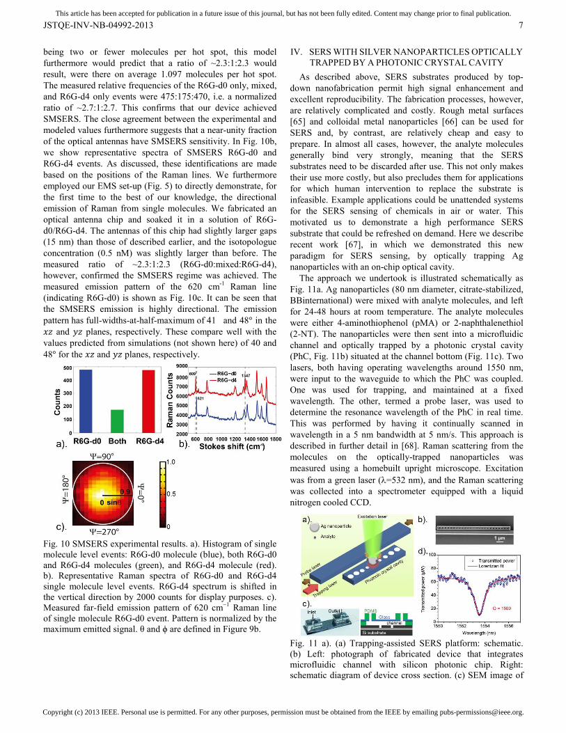
As described above, SERS substrates produced by top-down nanofabrication permit high signal enhancement and excellent reproducibility. The fabrication processes, however, are relatively complicated and costly. Rough metal surfaces [65] and colloidal metal nanoparticles [66] can be used for SERS and, by contrast, are relatively cheap and easy to prepare. In almost all cases, however, the analyte molecules generally bind very strongly, meaning that the SERS substrates need to be discarded after use. This not only makes their use more costly, but also precludes them for applications for which human intervention to replace the substrate is infeasible. Example applications could be unattended systems for the SERS sensing of chemicals in air or water. This motivated us to demonstrate a high performance SERS substrate that could be refreshed on demand. Here we describe recent work [67], in which we demonstrated this new paradigm for SERS sensing, by optically trapping Ag nanoparticles with an on-chip optical cavity.
The approach we undertook is illustrated schematically as Fig. 11a. Ag nanoparticles (80 nm diameter, citrate-stabilized, BBinternational) were mixed with analyte molecules, and left for 24-48 hours at room temperature. The analyte molecules were either 4-aminothiophenol (pMA) or 2-naphthalenethiol (2-NT). The nanoparticles were then sent into a microfluidic channel and optically trapped by a photonic crystal cavity (PhC, Fig. 11b) situated at the channel bottom (Fig. 11c). Two lasers, both having operating wavelengths around 1550 nm, were input to the waveguide to which the PhC was coupled. One was used for trapping, and maintained at a fixed wavelength. The other, termed a probe laser, was used to determine the resonance wavelength of the PhC in real time. This was performed by having it continually scanned in wavelength in a 5 nm bandwidth at 5 nm/s. This approach is described in further detail in [68]. Raman scattering from the molecules on the optically-trapped nanoparticles was measured using a homebuilt upright microscope. Excitation was from a green laser (λ=532 nm), and the Raman scattering was collected into a spectrometer equipped with a liquid nitrogen cooled CCD.
Fig. 11 a). (a) Trapping-assisted SERS platform: schematic. (b) Left: photograph of fabricated device that integrates microfluidic channel with silicon photonic chip. Right: schematic diagram of device cross section. (c) SEM image of
Copyright (c) 2013 IEEE. Personal use is permitted. For any other purposes, permission must be obtained from the IEEE by emailing [email protected].
This article has been accepted for publication in a future issue of this journal, but has not been fully edited. Content may change prior to final publication.
JSTQE-INV-NB-04992-2013 8
silicon photonic crystal cavity coupled to waveguide with a gap of 200 nm. (d) Photonic crystal cavity: measured transmission spectrum and Lorentzian curve fit.
Fabrication of the silicon PhC chip involved the following. The starting substrate was a silicon-on-insulator wafer having top silicon and buried oxide layers that were 220 nm and 3 µm thick, respectively. The wafer was cleaved and coated with negative-tone e-beam resist (HSQ, hydrogen silsesquioxane). Electron-beam lithography and reactive ion etching were then performed. The latter employed hydrogen bromide (HBr) gas as the etchant, enabling smooth and vertical sidewalls to be achieved. The chip was then dipped into 7:1 buffered oxide etch (BOE) solution to remove the HSQ. We then bonded a polydimethylsiloxane (PDMS, 100 µm thick) film, containing a 1 mm wide channel in its center, to the silicon chip. A glass coverslip (no. 1.5) was then bonded to the top of the PDMS. Two holes had been drilled in the coverslip with a CO2 laser. Two thick PDMS chunks were bonded to the coverslip, enabling inlet and outlet tubes to be connected to the device (Fig. 11c). The PhC and waveguide (Fig. 11b) were both 220 nm thick and 450 nm wide. The holes were shifted outward to form a cavity in the center. In addition, the hole diameters were made to gradually increase from the cavity center, to reduce the scattering loss from the cavity and to increase the quality factor. This was measured to be ~1500 (Fig. 11d).
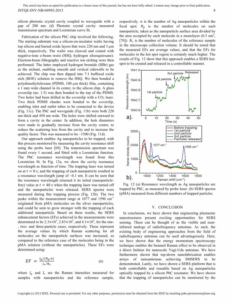
Our approach enables Ag nanoparticles to be trapped, with this process monitored by measuring the cavity resonance shift using the probe laser [69]. The transmission spectrum was found every 1 second, and fitted with a Lorentzian function. The PhC resonance wavelength was found from this Lorentzian fit. In Fig. 12a, we show the cavity resonance wavelength as function of time. The trapping laser was turned on at 𝑡 = 0 𝑠, and the trapping of each nanoparticle resulted in a resonance wavelength jump of ~0.1 nm. It can be seen that the resonance wavelength returned it its initial (nanoparticle-free) value at 𝑡 = 40 𝑠 when the trapping laser was turned off and the nanoparticles were released. SERS spectra were measured during this trapping process (Fig. 12b). The two peaks within the measurement range at 1077 and 1590 cm-1 originated from pMA molecules on the silver nanoparticles, and could be seen to grow stronger with the trapping of each additional nanoparticle. Based on these results, the SERS enhancement factors (EFs) achieved in the measurements were determined to be 2.3×10³, 2.83×10³, and 4.1×10³, for the one-, two- and three-particle cases, respectively. These represent the average values by which Raman scattering for all molecules on the nanoparticle surfaces was increased, as compared to the reference case of the molecules being in the pMA solution (without the nanoparticles). These EFs were determined using:
𝐸𝐹 = 𝐼𝑝 (𝑁𝑝∙𝑛)⁄𝐼𝑟 𝑁𝑟⁄ (6)
where 𝐼𝑝 and 𝐼𝑟 are the Raman intensities measured for samples with nanoparticles and the reference sample,
respectively. 𝑛 is the number of Ag nanoparticles within the focal spot. 𝑁𝑝 is the number of molecules on each nanoparticle, taken as the nanoparticle surface area divided by the area occupied by each molecule in a monolayer (0.3 nm2, [70]). 𝑁𝑟 is the number of molecules of the reference sample in the microscope collection volume. It should be noted that the measured EFs are average values, and that the EFs for molecules in the hot spot region is certainly much higher. The results of Fig. 12 show that this approach enables a SERS hot-spot to be created and released in a controllable manner.
Fig. 12 (a) Resonance wavelength as Ag nanoparticles are
trapped by PhC, as measured by probe laser. (b) SERS spectra (pMA) measured from different numbers of trapped particles.
V. CONCLUSION In conclusion, we have shown that engineering plasmonic
nanostructures present exciting opportunities for SERS sensing. These can be thought of as the visible and near-infrared analogs of radiofrequency antennas. As such, the existing body of engineering approaches from the field of radiofrequency antennas can be used advantageously. Here, we have shown that the energy momentum spectroscopy technique enables the beamed Raman effect to be observed in a direct fashion for nanoscale Yagi-Uda antennas. We have furthermore shown that top-down nanofabrication enables arrays of nanoantennas achieving SMSERS to be demonstrated. Lastly, we have shown a SERS platform that is both controllable and reusable based on Ag nanoparticles optically trapped by a silicon PhC resonator. We have shown that the trapping of nanoparticles can be monitored by the

Copyright (c) 2013 IEEE. Personal use is permitted. For any other purposes, permission must be obtained from the IEEE by emailing [email protected].
This article has been accepted for publication in a future issue of this journal, but has not been fully edited. Content may change prior to final publication.
JSTQE-INV-NB-04992-2013 9
resonance shift of the cavity. The nanoparticles can be released after a SERS measurement is made, and fresh nanoparticles trapped. In this way, a SERS substrate that is not only controllable and of high performance, but also continually replenishable, was demonstrated.
In closing, we comment on future directions in the field of plasmonic nanostructures for SERS. As described in this paper, the development of reproducible plasmonic nanostructures that achieve high enhancement factors and directionality is important due to the compelling need to overcome the fundamental problem that Raman cross sections are comparatively small. This will continue to be a vital goal in the future, and it is likely that progress in the field of plasmonics will lead to some dramatic advances. We note however that an equally important problem, partly addressed in the PhC trapping work described here, is that of getting the analyte molecule to the SERS hot spot. Here, the emerging field of optofluidics [71] could play an important role. Optofluidics refers to the combination of optics and microfluidics, with applications that include displays, biosensors, lab-on-chip devices, lenses, molecular imaging tools and energy. Recently, the theme of improving the SERS signal by concentrating the target molecules and metal nanoparticles within the detection zone of the optofluidic device has emerged. This has been achieved using packed silica microspheres that accumulate Ag nanoparticles and analyte molecules [72], an elastomeric collapse method to separate proteins [73], optoelectrofluidics [74], silver-coated magnetic microspheres [75], flow-through multihole capillaries [76], electrokinetic preconcentration [77], pinched channels to accumulate nanoparticles and analyte molecules [78], and engineered super-hydrophobic surfaces combined with plasmonics [79]. Many exciting possibilities exist, with further developments likely requiring not only practitioners from plasmonics and spectroscopy, but an interdisciplinary approach including individuals from the fields of fluid mechanics, chemistry and surface science.
REFERENCES [1] Mark L. Brongersma and Vladimir M. Shalaev, “The case for plasmonics,” Science vol. 328, pp. 440-441 (2010) [2] R. F. Oulton, V. J. Sorger, T. Zentgraf, R.-M. Ma, C. Gladden, L. Dai, G. Bartal, and X. Zhang, "Plasmon lasers at deep subwavelength scale," Nature 461, pp. 629-632 (2009) [3] M. A. Noginov, G. Zhu, A. M. Belgrave, R. Bakker, V. M. Shalaev, E. E. Narimanov, S. Stout, E. Herz, T. Suteewong, and U. Wiesner, "Demonstration of a spaser-based nanolaser," Nature 460, 1110-1112 (2009) [4] S. I. Bozhevolnyi, V. S. Volkov, E. Devaux, J. Y. Laluet, and T.W. Ebbesen, “Channel plasmon subwavelength waveguide components including interferometers and ring resonators,” Nature vol. 440, pp. 508–511, Mar. 2006. [5] L. Tang, S.E. Kocabas, S. Latif, A.K. Okyay, D-S Ly-Gagnon, K.C. Saraswat & D.A.B. Miller, “Nanometre-scale germanium photodetector enhanced by a near-infrared dipole antenna,” Nature Photon. vol. 2, pp. 226-229 (2008)
[6] W. Cai, J.S. White and M.L. Brongersma, “Compact, high-speed and power-efficient electrooptic plasmonic modulators,” Nano Lett. vol. 9, pp 4403–4411 (2009) [7] J. Homola, “Surface plasmon resonance sensors for detection of chemical and biological species,” Chem. Rev. vol. 108, pp. 462–493 (2008). [8] W.A. Challener, C. Peng, A.V. Itagi, D. Karns, W. Peng, Y. Peng, Xiao, M. Yang, X. Zhu, N.J. Gokemeijer, Y.-T. Hsia, G. Ju, R.E. Rottmayer, M.A. Seigler & E.C. Gage, “Heat-assisted magnetic recording by a near-field transducer with efficient optical energy transfer,” Nature Photon. vol. 3, pp. 220-224 (2009) [9] A. Roberts and L. Lin, “Plasmonic quarter-wave plate,” Opt. Lett. vol. 37, pp. 1820-1822 (2012) [10] T. Ellenbogen, K. Seo, and K.B. Crozier, "Chromatic Plasmonic Polarizers for Active Visible Color Filtering and Polarimetry," Nano Lett. vol. 12, pp. 1026-1031 (2012) [11] E.H. Khoo, E.P. Li, and K.B. Crozier, "A Plasmonic Waveplate Based on Subwavelength Nanoslits," Opt. Lett. vol. 36, pp. 2498-2500 (2011) [12] M. Righini, G. Volpe, C. Girard, D. Petrov, and R. Quidant, “Surface plasmon optical tweezers: tunable optical manipulation in the femtonewton range,” Phys. Rev. Lett. vol. 100, pp. 186804 (2008) [13] W. Zhang, L. Huang, C. Santschi, and O.J.F. Martin, “Trapping and sensing 10 nm metal nanoparticles using plasmonic dipole antennas,” Nano. Lett. vol. 10, pp. 1006–1011 (2010) [14] A. Zehtabi-Oskuie, H. Jiang, B. Cyr, D. Rennehan, A. Al-Balushi, R Gordon, "Double nanohole optical trapping: Dynamics and protein-antibody co-trapping," Lab Chip vol. 13, pp. 2563-2568 (2013). [15] K. Wang, E. Schonbrun, P. Steinvurzel & K.B. Crozier, "Trapping and rotating nanoparticles using a plasmonic nano-tweezer with an integrated heat sink," Nat. Commun. vol. 2, pp. 469 (2011) [16] K. Wang, E. Schonbrun, P. Steinvurzel, and K.B. Crozier, "Scannable Plasmonic Trapping Using a Gold Stripe," Nano Lett. vol. 10, pp. 3506 (2010) [17] K. Wang, E. Schonbrun, and K.B. Crozier, "Propulsion of Gold Nanoparticles with Surface Plasmon Polaritons: Evidence of Enhanced Optical Force from Near-Field Coupling between Gold Particle and Gold Film," Nano Lett. vol. 9, pp. 2623 (2009) [18] J Hu, S Lin, LC Kimerling, K Crozier, “Optical trapping of dielectric nanoparticles in resonant cavities,” Phys. Rev. A vol. 82, 053819 (2010) [19] V.M. Shalaev, “Transforming light,” Science vol. 322, pp. 384-386 (2008) [20] M. Fleischmann, P.J. Hendra, A.J. McQuillan, “Raman spectra of pyridine adsorbed at a silver electrode,” Chem. Phys. Lett. vol. 26, pp. 163 (1974) [21] D.L. Jeanmaire and R.P. Van Duyne, “Surface Raman spectroelectrochemistry: Part I. Heterocyclic, aromatic, and aliphatic amines adsorbed on the anodized silver electrode,” J. Electroanal. Chem. vol. 84, pp. 1 (1977) [22] J. Wessel , “Surface enhanced optical microscopy,” J. Opt. Soc. Am. B vol. 2, pp. 1538-1541 (1985)

Copyright (c) 2013 IEEE. Personal use is permitted. For any other purposes, permission must be obtained from the IEEE by emailing [email protected].
This article has been accepted for publication in a future issue of this journal, but has not been fully edited. Content may change prior to final publication.
JSTQE-INV-NB-04992-2013 10
[23] R.D. Grober, R.J. Schoelkopf, and D. E.Prober, “Optical antenna: Towards a unity efficiency near-field optical probe," Appl. Phys. Lett. vol. 70, 1354 (1997) [24] K.B. Crozier, A. Sundaramurthy , G.S. Kino, and C.F. Quate, “Optical antennas: resonators for local field enhancement,” J. Appl. Phys. vol. 94, pp. 4632 (2003) [25] L. Novotny, “Effective wavelength scaling for optical antennas,” Phys. Rev. Lett. vol. 98, pp. 266802 (2007) [26] W. Zhu, M.G. Banaee, D. Wang, Y. Chu, and K.B. Crozier, “Lithographically fabricated optical antennas with gaps well below 10 nm,” Small vol. 7, pp. 1761-1766 (2011) [27] E.C. Le Ru and P.G. Etchegoin, Principles of Surface-enhanced Raman Spectroscopy. Amsterdam, The Netherlands: Elsevier, 2009, pp. 91-97 [28] W.B. Cai, B. Ren, X.Q. Li, C.X. She, F.M. Liu, X.W. Cai, and W.Q. Tian, “Investigation of Surface-Enhanced Raman Scattering from Platinum Electrodes Using a Confocal Raman Microscope: Dependence of Surface Roughening Pretreatment,” Surf. Sci. vol. 406, 9–22 (2008) [29] Y. Chu, M.G. Banaee, and K.B. Crozier, “Double-resonance plasmon substrates for surface-enhanced Raman scattering with enhancement at excitation and Stokes frequencies,” ACS Nano vol. 4, pp. 2804-2810 (2010) [30] W.E. Moerner, New directions in single-molecule imaging and analysis,” Proc. Natl. Acad. Sci. U.S.A. vol. 104, pp. 12596–12602 (2007) [31] M. Moskovits,” Surface-enhanced spectroscopy,” Rev. Mod. Phys. vol. 57, pp. 783-826 (1985) [32] S.K. Saikin, Y. Chu, D. Rappoport, K.B. Crozier, and A. Aspuru-Guzik, "Separation of Electromagnetic and Chemical Contributions to Surface-Enhanced Raman Spectra on Nanoengineered Plasmonic Substrates," J. Phys. Chem. Lett. vol. 1, pp. 2740 (2010) [33] T.H. Reilly, S. Chang, J.D. Corbman, G.C. Schatz, and K.L. Rowlen, “Quantitative evaluation of plasmon enhanced Raman scattering from nanoaperture arrays,” J. Phys. Chem. C vol. 111, pp. 1689–1694 (2007) [34] D. Wang, T. Yang, and K.B. Crozier, "Optical antennas integrated with concentric ring gratings: electric field enhancement and directional radiation," Opt. Express vol. 19, pp. 2148−2157 (2011) [35] Y. Chu, W. Zhu, D. Wang and K.B. Crozier, "Beamed Raman: directional excitation and emission enhancement in a plasmonic crystal double resonance SERS substrate," Opt. Express vol. 19, pp. 20054-20068 (2011) [36] B. Liu, D. Wang, C. Shi, K.B. Crozier, and T. Yang, “Vertical optical antennas integrated with spiral ring gratings for large local electric field enhancement and directional radiation,” Opt. Express vol. 19, pp. 10049-10056 (2011) [37] D. Wang, W. Zhu, Y. Chu and K.B. Crozier, "High directivity optical antenna substrates for surface enhanced Raman scattering," Adv. Mater. vol. 24, pp. 4376–4380 (2012) [38] A. Ahmed and R. Gordon, “Directivity enhanced Raman spectroscopy using nanoantennas,” Nano Lett. vol. 11, 1800−1803 (2011) [39] M.A. Lieb, J.M. Zavislan, and L. Novotny, J. Opt. Soc. Am. B vol. 21, pp. 1210−1215 (2004) [40] W. Zhu, D. Wang and K.B. Crozier, "Direct observation of beamed Raman scattering," Nano Lett. vol. 12, pp. 6235-6243 (2012)
[41] T.H. Taminiau, S. Karaveli, N.F. van Hulst, and R. Zia, “Quantifying the magnetic nature of light emission,” Nat. Commun. vol. 3, pp. 979 (2012) [42] S. Uda, “Wireless beam of short electric waves,” J. IEE (Japan), pp. 273-282, March 1926, and pp. 1209-1219, November 1927 [43] H. Yagi, “Beam transmission of ultra short waves,” Proc. IRE, vol. 26, pp. 715-741, June 1928 [44] C.A. Balanis, Antenna theory analysis and design, 3rd ed, Hoboken, NJ: Wiley-Interscience, 2005, pp. 577-579 [45] T. Kosako, Y. Kadoya, and H.F. Hofmann, “Directional control of light by a nano-optical Yagi -Uda antenna,” Nature Photon. vol. 4, pp. 312−315 (2010) [46] D. Dregely, R. Taubert, J. Dorfmüller, R. Vogelgesang, K. Kern, and H. Giessen, “3D optical Yagi-Uda nanoantenna array,” Nat. Commun. vol. 2, pp. 267 (2011) [47] A.G. Curto, G. Volpe, T.H. Taminiau, M.P. Kreuzer, R. Quidant, and N.F. van Hulst, “Unidirectional Emission of a Quantum Dot Coupled to a Nanoantenna,” Science vol. 329, pp. 930−933 (2010) [48] S. Ramo, J.R. Whinnery and T. Van Duzer, Fields and waves in communication electronics,” 3rd ed., New York, NY: John Wiley and Sons, Inc. , 1994, pp. 641-642 [49] S. Nie and S.R. Emory, “Probing Single Molecules and Single Nanoparticles by Surface-Enhanced Raman Scattering,” Science vol. 275, pp. 1102−1106 (1997) [50] K. Kneipp, Y. Wang, H. Kneipp, L. Perelman, I. Itzkan, R. Dasari, and M. Feld, “Single Molecule Detection Using Surface-Enhanced Raman Scattering (SERS),” Phys. Rev. Lett. vol. 78, pp. 1667−1670 (1997) [51] A. Ahmed, and R. Gordon, “Single molecule directivity enhanced Raman scattering using nanoantennas,” Nano Lett. vol. 12, pp. 2625−30 (2012) [52] J. Dieringer, R.B. Lettan, K. Scheidt, and R.P. Van Duyne, “A Frequency Domain Existence Proof of Single-Molecule Surface-Enhanced Raman Spectroscopy,” J. Am. Chem. Soc. vol. 129, pp. 16249−56 (2007) [53] E.C. Le Ru, J. Grand, I. Sow, W.R.C. Somerville, P.G. Etchegoin, M. Treguer-Delapierre, G. Charron, N. Félidj, G. Lévi, and J. Aubard, “A Scheme for Detecting Every Single Target Molecule with Surface-Enhanced Raman Spectroscopy,” Nano Lett. vol. 11, pp. 5013−9 (2011) [54] S.L. Kleinman, E. Ringe, N. Valley, K.L. Wustholz, E. Phillips, K. Scheidt, G.C. Schatz, and R.P. Van Duyne, “Single-Molecule Surface-Enhanced Raman Spectroscopy of Crystal Violet Isotopologues: Theory and Experiment,” J. Am. Chem. Soc. vol. 133, 4115−22 (2011) [55] E.J. Blackie, E.C.; Le Ru, and P.J. Etchegoin, “Single-Molecule Surface-Enhanced Raman Spectroscopy of Nonresonant Molecules,” J. Am. Chem. Soc. vol. 131, pp. 14466−72 (2009) [56] Louis Brus, “Noble Metal Nanocrystals: Plasmon Electron Transfer Photochemistry and Single-Molecule Raman Spectroscopy,” Acc. Chem. Res. Vol. 41, pp. 1742 (2008) [57] J.P. Camden, J. Dieringer, Y. Wang, D.J. Masiello, L.D. Marks, G.C. Schatz, and R.P. Van Duyne, “Probing the structure of single-molecule surface-enhanced Raman scattering hot spots,” J. Am. Chem. Soc. vol. 130, pp. 12616−7 (2008)

Copyright (c) 2013 IEEE. Personal use is permitted. For any other purposes, permission must be obtained from the IEEE by emailing [email protected].
This article has been accepted for publication in a future issue of this journal, but has not been fully edited. Content may change prior to final publication.
JSTQE-INV-NB-04992-2013 11
[58] D. Wang , W. Zhu, M.D. Best, J.P. Camden, and K.B. Crozier, “Directional Raman Scattering from Single Molecules in the Feed Gaps of Optical Antennas,” Nano Lett. vol. 13, pp 2194–2198 (2013) [59] E.C. LeRu, M. Meyer, and P.G. Etchegoin, “Proof of single-molecule sensitivity in surface-enhanced Raman scattering (SERS) by means of a two-analyte technique,” J. Phys. Chem. B, vol. 110, pp. 1944-1948 (2006) [60] E.C. Le Ru, E. Blackie, M. Meyer and P.G. Etchegoin, “SERS enhancement factors: a comprehensive study,” J. Phys. Chem C vol. 111, pp. 13794-13803 (2007) [61] A. Kudelski and B. Pettinger, “SERS on carbon chain segments: monitoring locally surface chemistry,” Chem Phys Lett. vol. 321, pp. 356-362 (2000) [62] E. C. Le Ru, P. G. Etchegoin, and M. Meyer, “Enhancement factor distribution around a single surface-enhanced Raman scattering hot spot and its relation to single molecule detection,” J. Chemical Physics vol. 125, pp. 204701 (2006) [63] E. Blackie, E.C. Le Ru, M. Meyer, M. Timmer, B. Burkett, P. Northcote, and P.G. Etchegoin, “Bi-analyte SERS with isotopically edited dyes,” Phys. Chem. Chem. Phys. vol. 10, pp. 4147−53 (2008) [64] N. Mirsaleh-Kohan, V. Iberi, P.D. Simmons, N.W. Bigelow, A. Vaschillo, M.M. Rowland, M.D. Best, S.J. Pennycook, D.J. Masiello, B.S. Guiton, and J.P. Camden, “Single-Molecule Surface-Enhanced Raman Scattering: Can STEM/EELS Image Electromagnetic Hot Spots?,” J. Phys. Chem. Lett. vol. 3, pp. 2303−2309 (2012) [65] E.D. Diebold, N.H. Mack, S.K. Doorn, and E. Mazur, “Femtosecond laser-nanostructured substrates for surface-enhanced Raman scattering,” Langmuir vol. 25, pp. 1790−4 (2009) [66] L. Rivas, S. Sanchez-Cortes, J.V Garcia-Ramos, and G. Morcillo, “Growth of Silver Colloidal Particles Obtained by Citrate Reduction To Increase the Raman Enhancement Factor,” Langmuir vol. 17, pp. 574−577 (2001) [67] S. Lin, W. Zhu, Y. Jin, and K.B. Crozier, “Surface-Enhanced Raman Scattering with Ag Nanoparticles Optically Trapped by a Photonic Crystal Cavity,” Nano Lett. vol. 13, pp. 559 (2013) [68] S. Lin and K.B. Crozier, “Trapping-Assisted Sensing of Particles and Proteins Using On-Chip Optical Microcavities,” ACS Nano vol. 7, pp. 1725 (2013) [69] S. Lin and K.B. Crozier, "Planar silicon microrings as wavelength-multiplexed optical traps for storing and sensing particles," Lab Chip vol. 11, pp. 4047-4051 (2011) [70] C.S. Levin, S.W. Bishnoi, N.K. Grady, and N.J. Halas, “Determining the conformation of thiolated poly(ethylene glycol) on Au nanoshells by surface-enhanced Raman scattering spectroscopic assay," Anal. Chem. vol. 78, pp. 3277–81 (2006) [71] D. Psaltis, S.R. Quake and C. Yang, “Developing optofluidic technology through the fusion of microfluidics and optics,” Nature vol. 442, pp. 381-386 (2006) [72] S.H. Yazdi and I.M. White, “Multiplexed detection of aquaculture fungicides using a pump-free optofluidic SERS microsystem,” Analyst vol. 138, pp. 100-103 (2013) [73] I. Choi, Y. S. Huh and D. Erickson, “Size-selective concentration and label-free characterization of protein
aggregates using a Raman active nanofluidic device,” Lab Chip vol. 11, pp. 632–688 (2011) [74] H. Hwang, D. Han, Y.-J. Oh, Y.-K. Cho, K.-H. Jeong and J.-K. Park, “In situ dynamic measurements of the enhanced SERS signal using an optoelectrofluidic SERS platform,” Lab Chip vol. 11, pp. 2518–2525 (2011) [75] B. Han, N. Choi, K. H. Kim, D. W. Lim and J. Choo, “Application of Silver-Coated Magnetic Microspheres to a SERS-Based Optofluidic Sensor,” J. Phys. Chem. C vol. 115, pp. 6290–6296 (2011) [76] Y. Guo, M.K.K. Oo, K. Reddy and X. Fan, “Ultrasensitive Optofluidic Surface-Enhanced Raman Scattering Detection with Flow-through Multihole Capillaries,” ACS Nano, vol. 6, 381–388 (2012) [77] H. Cho, B. Lee, G.L. Liu, A. Agarwal and L.P. Lee, “Label-free and highly sensitive biomolecular detection using SERS and electrokinetic preconcentration,” Lab Chip vol. 9, pp. 3360–3363 (2009) [78] M. Wang, N. Jing, I.-H. Chou, G.L. Cote and J. Kameoka, “An optofluidic device for surface enhanced Raman spectroscopy,” Lab Chip vol. 7, 630–632 (2007) [79] F. De Angelis, F. Gentile, F. Mecarini, G. Das, M. Moretti, P. Candeloro, M.L. Coluccio, G. Cojoc, A. Accardo, C. Liberale, R.P. Zaccaria, G. Perozziello, L. Tirinato, A. Toma, G. Cuda, R. Cingolani and E. Di Fabrizio, “Breaking the diffusion limit with super-hydrophobic delivery of molecules to plasmonic nanofocusing SERS structures,” Nature Photon. vol. 5, pp. 682-687 (2011)
Kenneth B. Crozier (M’02–SM’12) received the B.Sc. and B.E. (Hons.) degrees in physics and electrical engineering from the University of Melbourne, Australia, in 1996. He received the M.S.E.E and Ph.D. degrees in electrical engineering from Stanford University, Stanford, CA, in 1999 and 2003, respectively.
From 2003 to 2004, he was a Postdoctoral Fellow at Stanford University. In 2004, he joined the faculty of Harvard University, Cambridge, MA, where he is now an Associate Professor of Electrical Engineering. His current research interests include micro- and nano-optics, including plasmonics for surface enhanced Raman spectroscopy and optical forces, optofluidics and semiconductor nanowires. Prof. Crozier is a Senior Member of the Optical Society (OSA) and of the International Society for Optics and Photonics (SPIE). He was awarded the L.R. East Medal by the University of Melbourne. In 2008, he was a recipient of a CAREER award from the National Science Foundation (NSF) and a Loeb Chair at Harvard, an endowed position.

Copyright (c) 2013 IEEE. Personal use is permitted. For any other purposes, permission must be obtained from the IEEE by emailing [email protected].
This article has been accepted for publication in a future issue of this journal, but has not been fully edited. Content may change prior to final publication.
JSTQE-INV-NB-04992-2013 12
Wenqi Zhu received the B.S. degree in electrical engineering from Tsinghua University, China, in 2005, and M.E. degree in electrical and computer engineering from University of Utah, in 2008. He is presently working towards the Ph.D. degree in electrical engineering at Harvard University. His research interests
include optical antennas, nanofabrication and surface-enhanced Raman spectroscopy.
Dongxing Wang received his B.E. degree in Information and Electronic Engineering from Zhejiang University, China, in 2004. From 2004 to 2008, he was a graduate student in Electrical Engineering in Zhejiang University, China. He is currently pursuing the PhD degree in Electrical Engineering at
Harvard University, Cambridge, MA. His research interest includes the development of plasmonic structures, with an emphasis on applications in surface enhanced Raman spectroscopy, metamaterial and fabrication of nano-optics devices.
Shiyun Lin received the B.S. degree in materials science and engineering from Tsinghua University, Beijing, China in 2004, M.S. degree in materials engineering from the University of Tokyo, Tokyo, Japan in 2008 and Ph.D. degree in engineering science from Harvard University, Cambridge, MA, in 2013.
He is now a Staff Engineer in the Photonics, Interconnects, and Packaging Group at Oracle Labs, San Diego, CA. His current research interests include silicon photonics and advanced packaging for optical inter/intra-chip interconnects.
Michael D. Best received the B.S. degree in chemistry from
Boston College, Chestnut Hill, MA, in 1997, and the Ph.D. degree in chemistry from the University of Texas at Austin in 2002. From 2002-2005, he was a research assistant at The Scripps Research Institute in La Jolla, CA. In 2005, he joined the faculty at the University of Tennessee at Knoxville, where he is
currently an Associate Professor. His research interests generally involve the design, synthesis and analysis of small molecule probes for characterizing chemical and biological systems.
Mr. Best’s awards include the American Institute of Chemists Awards for Outstanding Senior Majoring in Chemistry as well as a National Science Foundation CAREER Award.
Jon P. Camden received the B.S. degree in chemistry and music from the University of Notre Dame, South Bend, IN, in 2000, and the Ph.D. degree in physical chemistry from Stanford University, Stanford, CA in 2005. From 2005-2008, he was a postdoctoral researcher at Northwestern University in
Evanston, IL. In 2008 he joined the faculty of the University of Tennessee, Knoxville, TN where he is an Assistant Professor of Chemistry. His current research interests include the optical properties of metal nanoparticles, ultrasensitive detection, surface enhanced spectroscopy, and chemical reaction dynamics.
Prof. Camden is a member of the American Chemical Society and Phi Beta Kappa. His awards include a National Science Foundation Graduate Fellowship (2001-2004), a National Science Foundation CAREER award (2012), the Research and Creative Achievement Award from the University of Tennessee (2013) and the Gleb Mamantov Professorship (2013).