Embed Size (px)
Citation preview
PLASMONICS
A Technical Report
Submitted on the occasion of COGNOSCENTI, SANKALP: 2007
Sankalp- 2007
BY
PRABHAT KIRAN PADHY Roll # ECE200610020
&
NILADRI BIHARI NAYAK Roll # ECE200626388
NATIONAL INSTITUTE OF SCIENCE &TECHNOLOGY PALUR HILLS, BERHAMPUR, ORISSA – 761008, INDIA
2
ABSTRACT
Optical fibers now span the globe, guiding light signals that convey voluminous streams of
voice communications and vast amounts of data.Hence the drive towards highly integrated
optical devices and circuits for use in high-speed communication technologies and in future
all-optical photonic chips has generated considerable interest in the unique properties of
surface plasmon polaritons (SPP). SPP are electromagnetic waves that are confined to the
interface between materials with dielectric constants of opposite sign. This confinement of
the SPP field to the interface opens the possibility of overcoming the diffraction limit
encountered in classical optics and of realizing planar nanoscale, highly integrated optical
devices.
In our presentation we will discuss a new approach for generating intense nano-scale SPP
spots. The constructive interference of SPPs launched by nanometric holes allows focusing
SPP into an intense sub-wavelength spot of 380 nm width. Near-field scanning optical
microscopy is used to image the local SPP fields. The resulting SPP intensity patterns are
accurately described in calculations based on dipolar SPP sources at each hole as well as on
Finite-Difference Time-Domain simulations. The combination of a focusing array and
nano-wave guide may serve a basic element in planar nano-photonic circuits. Possible
applications to surface-enhanced optical sensing of molecular species will be discussed.
In a nutshell, it is a technology that squeezes electromagnetic waves into minuscule
structures that may yield a new generation of superfast computer chips and ultrasensitive
molecular detectors.
3
TABLE OF CONTENTS
ABSTRACT ....................................................................................................................... 2
TABLE OF CONTENTS .................................................................................................. 3
1. INTRODUCTION ......................................................................................................... 4
2. WHAT IS PLASMONICS? .......................................................................................... 4
3. WHY A NEW TECHNOLOGY? ................................................................................. 5
4. FEATURES OF PLASMONICS:................................................................................ 6
5. UNIQUE PROPERTIES OF SURFACE PLASMONS: .......................................... 9
6. PLASMONICS: A MATHEMATICAL APPROACH: .............................................. 10
7. APPLICATIONS ......................................................................................................... 12
PLASMONIC LED : ................................................................................................... 12 SPASER - PLASMONIC ANALOG OF LASER : ................................................. 13
PLASMONSTER - A FASTER CHIP: ..................................................................... 13 INVISIBILITY CLOAKS ............................................................................................. 13 PLASMONIC NANOCELL THERAPY: ................................................................... 14
8. CONCLUSION: .......................................................................................................... 15
9. REFERENCE: ............................................................................................................ 16
4
1. INTRODUCTION
Plasma is a medium with equal concentration of positive and negative charges, of which
at least one charge type is mobile. With the increasing quest for transporting large
amounts of data at a fast speed along with miniaturization both electronics and photonics
are facing limitations.In physics, the plasmon is the quasiparticle resulting from the
quantization of plasma oscillations just as photons and phonons are quantizations of light
and sound waves, respectively. Thus, plasmons are collective oscillations of the free
electron gas density, often at optical frequencies. They can also couple with a photon to
create a third quasiparticle called a plasma polariton Scientists are now more inclined
from Photonics to Plasmonics. It opens the new era in optical communication.
2. WHAT IS PLASMONICS?
Definition:
A technology that squeezes electromagnetic waves into minuscule structures may yield a
new generation of superfast computer chips and ultrasensitive molecular detectors.
Mechanism:
Light beam striking a metal surface generates plasmons, electron density waves that can
carry huge amounts of data.
If focused on surface etched with circular groove the beam produces concentric waves
organizing electrons into high & low density rings.
5
3. WHY A NEW TECHNOLOGY?
Optical fibers now span the globe, guiding light signals that convey voluminous streams
of voice communications and vast amounts of data. This gargantuan capacity has led
some researchers to prophesy that photonic devices--which channel and manipulate
visible light and other electromagnetic waves--could someday replace electronic circuits
in microprocessors and other computer chips. Unfortunately, the size and performance of
photonic devices are constrained by the diffraction limit; because of interference between
closely spaced light waves, the width of an optical fiber carrying them must be at least
half the light's wavelength inside the material. For chip-based optical signals, which will
most likely employ near- infrared wavelengths of about 1,500 nanometers (billionths of a
meter), the minimum width is much larger than the smallest electronic devices currently
in use; some transistors in silicon integrated circuits, for instance, have features smaller
than 100 nanometers.
Recently, however, scientists have been working on a new technique for transmitting
optical signals through minuscule nanoscale structures. In the 1980s researchers
experimentally confirmed that directing light waves at the interface between a metal and
a dielectric (a nonconductive material such as air or glass) can, under the right
circumstances, induce a resonant interaction between the waves and the mobile electrons
at the surface of the metal. (In a conductive metal, the electrons are not strongly attached
to individual atoms or molecules.) In other words, the oscillations of electrons at the
surface match those of the electromagnetic field outside the metal. The result is the
generation of surface plasmons--density waves of electrons that propagate along the
interface like the ripples that spread across the surface of a pond after you throw a stone
into the water.
6
4. FEATURES OF PLASMONICS:
Over the past decade investigators have found that by creatively designing the metal-
dielectric interface they can generate surface plasmons with the same frequency as the
outside electromagnetic waves but with a much shorter wavelength. This phenomenon
could allow the plasmons to travel along nanoscale wires called interconnects, carrying
information from one part of a microprocessor to another. Plasmonic interconnects would
be a great boon for chip designers, who have been able to develop ever smaller and faster
transistors but have had a harder time building minute electronic circuits that can move
data quickly across the chip.
The term "plasmonics" came into existence in 2000 from the word „plasmon‟, sensing
that research in this area could lead to an entirely new class of devices. Ultimately it may
be possible to employ plasmonic components in a wide variety of instruments, using
them to improve the resolution of microscopes, the efficiency of light-emitting diodes
(LEDs) and the sensitivity of chemical and biological detectors. Scientists are also
considering medical applications, designing tiny particles that could use plasmon
resonance absorption to kill cancerous tissues, for example. And some researchers have
even theorized that certain plasmonic materials could alter the electromagnetic field
around an object to such an extent that it would become invisible. Although not all these
potential applications may prove feasible, investigators are eagerly studying plasmonics
because the new field promises to literally shine a light on the mysteries of the
nanoworld.
For millennia, alchemists and glassmakers have unwittingly taken advantage of
plasmonic effects when they created stained-glass windows and colorful goblets that
incorporated small metallic particles in the glass. The most notable example is the
Lycurgus cup, a Roman goblet dating from the fourth century A.D. and now held in the
British Museum. Because of plasmonic excitation of electrons in the metallic particles
suspended within the glass matrix, the cup absorbs and scatters blue and green light--the
relatively short wavelengths of the visible spectrum. When viewed in reflected light, the
plasmonic scattering gives the cup a greenish hue, but if a white light source is placed
7
within the goblet, the glass appears red because it transmits only the longer wavelengths
and absorbs the shorter ones.
The field of plasmonics received another boost with the discovery of novel
"metamaterials"--materials in which electron oscillations can result in astounding optical
properties. Two new classes of tools have also accelerated progress in plasmonics: recent
increases in computational power have enabled investigators to accurately simulate the
complex electromagnetic fields generated by plasmonic effects, and novel methods for
constructing nanoscale structures have made it possible to build and test ultrasmall
plasmonic devices and circuits.
At first glance, the use of metallic structures to transmit light signals seems impractical,
because metals are known for high optical losses. The electrons oscillating in the
electromagnetic field collide with the surrounding lattice of atoms, rapidly dissipating the
field's energy. But the plasmon losses are lower at the interface between a thin metal film
and a dielectric than inside the bulk of a metal because the field spreads into the
nonconductive material, where there are no free electrons to oscillate and hence no
energy-dissipating collisions. This property naturally confines plasmons to the metallic
surface abutting the dielectric; in a sandwich with dielectric and metal layers, for
example, the surface plasmons propagate only in the thin plane at the interface.
Because these planar plasmonic structures act as waveguides, shepherding the
electromagnetic waves along the metal-dielectric boundary, they could be useful in
routing signals on a chip. Although an optical signal suffers more loss in a metal than in a
dielectric such as glass, a plasmon can travel in a thin- film metal waveguide for several
centimeters before dying out. The propagation length can be maximized if the waveguide
employs an asymmetric mode, which pushes a greater portion of the electromagnetic
energy away from the guiding metal film and into the surrounding dielectric, thereby
lowering loss. Because the electromagnetic fields at the top and bottom surfaces of the
metal film interact with each other, the frequencies and wavelengths of the p lasmons can
be adjusted by changing the thickness of the film.
8
To generate plasmons that can propagate through nanoscale wires, researchers have
explored more complex waveguide geometries that can shrink the wavelength of the
signal by squeezing it into a narrow space.
Fortunately, the absorption losses can be minimized by turning the plasmonic waveguides
inside out, putting the dielectric at the core and surrounding it with metal. In this device,
called a plasmon slot waveguide, adjusting the thickness o f the dielectric core changes
the wavelength of the plasmons. It is shown that plasmon slot waveguides are capable of
transmitting a signal as far as tens of microns.
Plasmonics can thus generate signals in the soft x-ray range of wavelengths (between 10
and 100 nanometers) by exciting materials with visible light. The wavelength can be
reduced by more than a factor of 10 relative to its free-space value, and yet the frequency
of the signal remains the same. (The fundamental relation between the two--frequency
times wavelength equals the speed of light-- is preserved because the electromagnetic
waves slow as they travel along the metal-dielectric interface.) This striking ability to
shrink the wavelength opens the path to nanoscale plasmonic structures that could replace
purely electronic circuits containing wires and transistors.
Just as lithography is now used to imprint circuit patterns on silicon chips, a similar
process could mass-produce minuscule plasmonic devices with arrays of narrow
dielectric stripes and gaps. These arrays would guide the waves of positive and negative
charge on the metal surface; the alternating charge densities would be very much akin to
the alternating current traveling along an ordinary wire. But because the frequency of an
optical signal is so much higher than that of an electrical one--more than 400,000
gigahertz versus 60 hertz--the plasmonic circuit would be able to carry much more data.
Moreover, because electrical charge does not travel from one end of a plasmonic circuit
to another--the electrons bunch together and spread apart rather than streaming in a single
direction the device is not subject to resistance and capacitance effects that limit the data-
carrying capacity of integrated circuits with electrical interconnects.
Plasmonic circuits would be even faster and more useful if researchers could devise a
"plasmonster" switch--a three-terminal plasmonic device with transistor like properties.
9
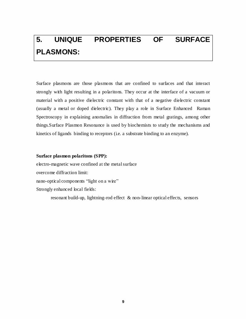
5. UNIQUE PROPERTIES OF SURFACE
PLASMONS:
Surface plasmons are those plasmons that are confined to surfaces and that interact
strongly with light resulting in a polaritons. They occur at the interface of a vacuum or
material with a positive dielectric constant with that of a negative dielectric constant
(usually a metal or doped dielectric). They play a role in Surface Enhanced Raman
Spectroscopy in explaining anomalies in diffraction from metal gratings, among other
things.Surface Plasmon Resonance is used by biochemists to study the mechanisms and
kinetics of ligands binding to receptors (i.e. a substrate binding to an enzyme).
Surface plasmon polaritons (SPP):
electro-magnetic wave confined at the metal surface
overcome diffraction limit:
nano-optical components “light on a wire”
Strongly enhanced local fields:
resonant build-up, lightning-rod effect & non- linear optical effects, sensors
10
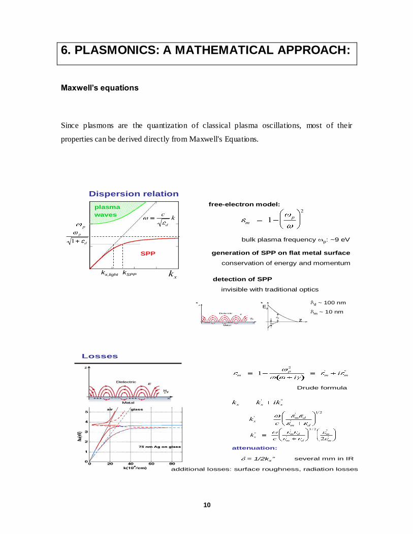
6. PLASMONICS: A MATHEMATICAL APPROACH:
Maxwell’s equations
Since plasmons are the quantization of classical plasma oscillations, most of their
properties can be derived directly from Maxwell's Equations.
p
p
1 d
kx
c
d
k
SPP
plasma
waves
Dispersion relation
m 1p
2
free-electron model:
bulk plasma frequency p: ~9 eV
kx,light kSPP
generation of SPP on flat metal surface
conservation of energy and momentum
detection of SPP
invisible with traditional optics
d ~ 100 nm
m ~ 10 nm
z
Ez
m 1p
2
i m
' i m"
attenuation:
= 1/2kx” several mm in IR
Losses
kx kx' ikx
"
kx'
c
m
'
d
m
'
d
1 2
kx"
c
m
'
d
m
'
d
3 / 2
m
"
2 m
'
Drude formula
additional losses: surface roughness, radiation losses
11
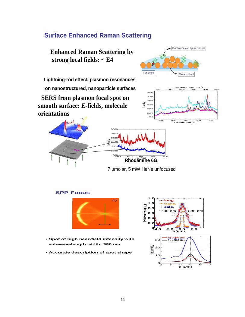
Surface Enhanced Raman Scattering
Lightning-rod effect, plasmon resonances
on nanostructured, nanoparticle surfaces
Rhodamine 6G,
7 µmolar, 5 mW HeNe unfocused
SERS from plasmon focal spot on
smooth surface: E-fields, molecule
orientations
Enhanced Raman Scattering by
strong local fields: ~ E4
SPP Focus
• Spot of high near-field intensity with
sub-wavelength width: 380 nm
• Accurate description of spot shape
12
7. APPLICATIONS
PLASMONIC LED :
Plasmonic materials may also revolutionize the lighting industry by making LEDs bright
enough to compete with incandescent bulbs. Beginning in the 1980s, researchers
recognized that the plasmonic enhancement of the electric field at the metal-dielectric
boundary could increase the emission rate of luminescent dyes placed near the metal's
surface. More recently, it has become evident that this type of field enhancement can also
dramatically raise the emission rates of Quantum dots and quantum wells--tiny
semiconductor structures that absorb and emit light--thus increasing the efficiency and
brightness of solid-state LEDs. It is demonstrated that coating the surface of a gallium
nitride LED with dense arrays of plasmonic nanoparticles (made of silver, gold or
aluminum) could increase the intensity of the emitted light 14-fold.
Furthermore, plasmonic nanoparticles may enable researchers to develop LEDs made of
silicon. Such devices, which would be much cheaper than conventional LEDs composed
of gallium nitride or gallium arsenide, are currently held back by their low rates of light
emission. It is found that coupling silver or gold plasmonic nanostructures to silicon
quantum-dot arrays could boost their light emission by about 10 times. Moreover, it is
possible to tune the frequency of the enhanced emissions by adjusting the dimensions of
the nanoparticle. Careful tuning of the plasmonic resonance frequency and precise control
of the separation between the metallic particles and the semiconductor materials may
enable us to increase radiative rates more than 100-fold, allowing silicon LEDs to shine
just as brightly as traditional devices.
13
SPASER - PLASMONIC ANALOG OF LASER :
The acronym SPASER stands for Surface Plasmon Amplification of Stimulated
Emission of Radiation. It can be fabricated using semiconductor quantum dots and
metal particles. Radiative energy from the quantum dots would be transformed into
plasmons, which would then be amplified in a plasmonic resonator. Because the
plasmons generated by a SPASER would be much more tightly localized than a
conventional laser beam, the device could operate at very low power and selectively
excite very small objects. As a result, SPASERs could make spectroscopy more sensitive
and pave the way for hazardous-materials detectors that could identify minute amounts of
chemicals or viruses.
PLASMONSTER - A FASTER CHIP:
Slot waveguides could significantly boost the speed of computer chips by rapidly
funneling large amounts of data to the circuits that perform logical operations. The
Plasmonsters are composed of slot waveguides that measure 100nm across at their
broadest points and only 20nm across at the intersection.
INVISIBILITY CLOAKS
The most fascinating potential application of plasmonics would be the invention of an
invisibility cloak. A material's refractive index is the ratio of the speed of light in a
vacuum to the speed of light in the material. Exciting a plasmonic structure with radiation
that is close to the structure's resonant frequency can make its refractive index equal to
air's, meaning that it would neither bend nor reflect light. The structure would absorb
light, but if it were laminated with a material that produces optical gain--amplifying the
transmitted signal just as the resonator in a SPASER would--the increase in intensity
would offset the absorption losses. The structure would become invisible, at least to
radiation in a selected range of frequencies.
14
A true invisibility cloak, however, must be able to hide anything within the structure and
work for all frequencies of visible light. It is showed that a shell of metamaterials can
reroute the electromagnetic waves traveling through it, diverting them around a spherical
region within.
PLASMONIC NANOCELL THERAPY:
The potential uses of plasmonic devices go far beyond computing. Nanoshell that
consists of a thin layer of gold--typically about 10 nanometers thick--deposited around
the entire surface of a silica particle about 100 nanometers across. Exposure to
electromagnetic waves generates electron oscillations in the gold shell; because of the
coupling interaction between the fields on the shell's inner and outer surfaces, varying the
size of the particle and the thickness of the gold layer changes the wavelength at which
the particle resonantly absorbs energy. In this way, investigators can design the
nanoshells to selectively absorb wavelengths as short as a few hundred nanometers (the
blue end of the visible spectrum) or as long as nearly 10 microns (the near infrared).
This phenomenon has turned nanoshells into a promising tool for cancer treatment. Ha las,
working with her Rice colleague Jennifer West, injected plasmonic nanoshells into the
bloodstream of mice with cancerous tumors and found that the particles were nontoxic.
What is more, the nanoshells tended to embed themselves in the rodents' cancero us
tissues rather than the healthy ones because more blood was circulated to the fast-
growing tumors. The nanoshells can also be attached to antibodies to ensure that they
target cancers.
Fortunately, human and animal tissues are transparent to radiation at certain infrared
wavelengths. When the researchers directed near- infrared laser light through the mice's
skin and at the tumors, the resonant absorption of energy in the embedded nanoshells
raised the temperature of the cancerous tissues from about 37 degrees Celsius to about 45
degrees C.
15
The photothermal heating killed the cancer cells while leaving the surrounding healthy
tissue unharmed. In the mice treated with nanoshells, all signs of cancer disappeared
within 10 days; in the control groups, the tumors continued to grow rapidly.
8. CONCLUSION:
The ideas of Plasmonics illustrate the rich array of optical properties that inspire
researchers in this field. By studying the elaborate interplay between electromagnetic
waves and free electrons, investigators have identified new possibilities for transmitting
data in our integrated circuits, illuminating our homes and fighting cancer. Further
exploration of these intriguing plasmonic phenomena may yield even more exciting
discoveries and inventions interactions between electromagnetic waves and matter. That
includes laser-plasma and laser-solid interactions, nano-photonics, and plasmonics. The
future challenge may be (a) developing high-gradient accelerators of charged particles
(table-top colliders!), and (b) designing novel nanostructures that will contribute to
nanoscale optical imaging and spectroscopy of chemicals and biomolecules.

16
9. REFERENCE:
Scientific American India, April-2007 Issue
Optical fibres and fibre optic communication systems,Subir K Sarkar, S.Chand
Publications
www.sciam.co.in
www.wikipedia.co.in
www.centralchronicle.co.in