Embed Size (px)
Citation preview
Plasmonic field enhancement and SERSin the effective mode volume picture
Stefan A. MaierCentre for Photonics and Photonic Materials, Department of Physics, University of Bath,
Bath BA2 7AY, UK
Abstract: The controlled creation of nanometric electromag-netic field confinement via surface plasmon polariton excitations inmetal/insulator/metal heterostructures is described via the concept of aneffective electromagnetic mode volume Veff. Extensively used for thedescription of dielectric microcavities, its extension to plasmonics providesa convenient figure of merit and allows comparisons with dielectric coun-terparts. Using a one-dimensional analytical model and three-dimensionalfinite-difference time-domain simulations, it is shown that plasmoniccavities with nanometric dielectric gaps indeed allow for physical as wellas effective mode volumes well below the diffraction limit in the gapmaterial, despite significant energy penetration into the metal. In thispicture, matter-plasmon interactions can be quantified in terms of qualityfactor Q and Veff, enabling a resonant cavity description of surface enhancedRaman scattering.
© 2006 Optical Society of America
OCIS codes: (240.6680) Surface plasmons; (230.5750) Resonators; (170.5660) Raman Spec-troscopy
References and links1. S. A. Maier and H. A. Atwater, ”Plasmonics: Localization and guiding of electromagnetic energy in
metal/dielectric structures,” J. Appl. Phys. 98, 011,101 (2005).2. S. A. Maier, P. G. Kik, H. A. Atwater, S. Meltzer, E. Harel, B. E. Koel, and A. A. G. Requicha, ”Local detection
of electromagnetic energy transport below the diffraction limit in metal nanoparticle plasmon waveguides,” Nat.Mat. 2, 229–232 (2003).
3. W. L. Barnes, A. Dereux, and T. Ebbesen, ”Surface plasmon subwavelength optics,” Nature 424, 824–830 (2002).4. K. Kneipp, Y. Wang, H. Kneipp, L. T. Perelman, I. Itzkan, R. R. Dasari, and M. S. Feld, ”Single molecule
detection using surface-enhanced Raman scattering (SERS),” Phys. Rev. Lett. 78, 1667 (1997).5. S. M. Nie and S. R. Emery, ”Probing single molecules and single nanoparticles by surface-enhanced Raman
scattering,” Science 275, 1102 (1997).6. H. Xu, J. Aizpurua, M. Kaell, and P. Apell, ”Electromagnetic contributions to single-molecule sensitivity in
surface-enhanced Raman scattering,” Phys. Rev. E 62, 4318–4324 (2000).7. A. Sundaramurthy, K. B. Crozier, G. S. Kino, D. P. Fromm, P. J. Schuck, and W. E. Moerner, ”Field enhancement
and gap-dependent resonance in a system of two opposing tip-to-tip Au nanotriangles,” Phys. Rev. B. 72, 165409(2005)
8. H. Kimble, ”Structure and Dynamics in Cavity Quantum Electrodynamics,” pp. 203–266 (Academic Press,Boston, 1994).
9. D. J. Norris, M. Kuwata-Gonokami, and W. E. Moerner, ”Excitation of a single molecule on the surface of aspherical microcavity,” Appl. Phys. Lett. 71, 297–299 (1997).
10. R. K. Chang and A. J. Campillo, eds., ”Optical Processes in Microcavities” (World Scientific, Singapore, 1996).11. D. W. Vernooy, V. S. Ilchenko, H. Mabuchi, E. W. Streed, and H. J. Kimble, ”High-Q measurements of fused-
silica microspheres in the near infrared,” Opt. Lett. 23, 247–249 (1998).12. D. K. Armani, T. J. Kippenberg, S. M. Spillane, and K. J. Vahala, ”Ultra-high-Q toroid microcavity on a chip,”
Nature 421, 925–928 (2003).
#10114 - $15.00 USD Received 3 January 2006; received 28 February 2006; accepted 28 February 2006
(C) 2006 OSA 6 March 2006 / Vol. 14, No. 5 / OPTICS EXPRESS 1957
13. A. F. J. Levi, S. L. McCall, S. J. Pearton, and R. A. Logan, ”Room Temperature Operation of SubmicrometreRadius Disk Laser,” Electron. Lett. 29, 1666–1667 (1993).
14. J. D. Joannopoulos, R. D. Meade, and J. N. Winn, ”Photonic Crystals” (Princeton University Press, Princeton,New Jersey, 1995).
15. O. Painter, R. K. Lee, A. Yariv, A. Scherer, J. D. O’Brien, P. D. Dapkus, and I. Kim, ”Two-Dimensional PhotonicBand-Gap Defect Mode Laser,” Science 284, 1819–1824 (1999).
16. W. Vogel and D.-G. Welsch, ”Lectures on Quantum Optics” (Akademie Verlag GmbH, Berlin, Federal Republicof Germany, 1994).
17. E. M. Purcell, ”Spontaneous emission probabilities at radio frequencies,” Phys. Rev. 69, 681 (1946).18. A. B. Matsko, A. A. Savchenkov, R. J. Letargat, V. S. Ilchenko, and L. Maleki, ”On cavity modification of
stimulated Raman scattering,” J. Opt. B: Quantum Semiclass. Opt. 5, 272–278 (2003).19. M. Kerker, D.-S. Wang, and H. Chew, ”Surface enhanced Raman scattering (SERS) by molecules adsorbed at
spherical particles: errata,” Appl. Opt. 19, 4159–4147 (1980).20. B. Prade, J. Y. Vinet, and A. Mysyrowicz, ”Guided optical waves in planar heterostructures with negative dielec-
tric constant,” Phys. Rev. B 44, 13,556–13,572 (1991).21. P. B. Johnson and R. W. Christy, ”Optical constants of the noble metals,” Phys. Rev. B 6, 4370–4379 (1972).22. R. Loudon, ”The propagation of electromagnetic energy through an absorbing dielectric,” J. Phys. A 3, 233–245
(1970).23. R. Ruppin, ”Electromagnetic energy density in a dispersive and absorptive material,” Phys. Lett. A 299, 309–312
(2002).24. J. Takahara, S. Yamagishi, H. Taki, A. Morimoto, and T. Kobayashi, ”Guiding of a one-dimensional optical beam
with nanometer diameter,” Opt. Lett. 22, 475 (1997).25. L. C. Andreani, G. Panzarini, and J.-M. Gerard, ”Strong-coupling regime for quantum boxes in pillar microcavi-
ties: Theory,” Phys. Rev. B 60, 13,276 (1999).26. M. A. Ordal, L. L. Long, R. J. Bell, R. R. Bell, R. W. Alexander, and C. A. Ward, ”Optical properties of the metals
Al, Co, Cu, Au, Fe, Pb, Ni, Pd, Pt, Ag, Ti, and W in the infrared and far infrared,” Appl. Opt. 22, 1099–1119(1983).
27. I. A. Larkin, M. I. Stockman, M. Achermann, and V. I. Klimov, ”Dipolar emitters at nanoscale proximity of metalsurfaces: Giant enhancement of relaxation in microscopic theory,” Phys. Rev. B 69, 121403(R) (2004).
28. H. A. Haus, ”Waves and Fields in Optoelectronics”, 1st ed. (Prentice-Hall, Englewood Cliffs, New Jersey 07632,1984).
29. S. M. Spillane, T. J. Kippenberg, and K. J. Vahala, ”Ultralow-threshold Raman laser using spherical dielectricmicrocavity,” Nature 415, 621–623 (2002).
30. T. Klar, M. Perner, S. Grosse, G. von Plessen, W. Spirkl, and J. Feldmann, ”Surface-plasmon resonances in singlemetallic nanoparticles,” Phys. Rev. Lett. 80, 4249–4252 (1998).
31. V. A. Shubin, W. Kim, V. P. Safonov, A. K. Sarychev, R. L. Armstrong, and V. M. Shalaev, ”Surface-plasmon-enhanced radiation effects in confined photonic systems,” J. Lightwave Technol. 17, 2183–2190 (1999).
32. E. Hinds, ”Pertubative cavity quantum electrodynamics”, pp. 1–56 (Academic Press, Boston, 1994).33. W. L. Barnes, ”Electromagnetic Crystals for Surface Plasmon Polaritons and the Extraction of Light from Emis-
sive Devices,” J. Lightwave Technol. 17, 2170–2182 (1999).34. J. Vuckovic, M. Loncar, and A. Scherer, ”Surface plasmon enhanced light-emitting diode,” IEEE J. Quantum
Electron. 36, 1131–1144 (2000).
1. Introduction
In recent years, the ever-increasing research efforts in the field of plasmonics - the study ofelectromagnetic field confinement and enhancement via surface plasmon polaritons (SPPs) -have led to a number of important advances towards the goal of a nanophotonic infrastructurefor confining and guiding electromagnetic radiation [1]. Recent examples include the creationof metal nanoparticle plasmon waveguide [2] and other sub-wavelength photonic devices [3],the fabrication of which is enabled by nanofabrication tools such as electron beam lithography.However, one of the most prominent application of SPPs and localized plasmons, single mole-cule surface enhanced Raman scattering (SERS)[4, 5], has up to now not been described in acontext of field enhancement in designed metal nanoscale cavities. The single molecule sensi-tivity relies on light localization in hot-spots on a roughened silver (Ag) surface where random,nanometer-sized junctions between surface protrusions are believed to form cavity-like struc-tures for field enhancement [6]. As a step towards a controlled sensing platform for SERS [7],here the enhancement process is presented from a waveguide-to-cavity-coupling point of view,
#10114 - $15.00 USD Received 3 January 2006; received 28 February 2006; accepted 28 February 2006
(C) 2006 OSA 6 March 2006 / Vol. 14, No. 5 / OPTICS EXPRESS 1958
which requires a careful look at the energetics of plasmonic energy localization in metallicnanocavities.
Optical cavities in general provide an intriguing way to alter the interaction of light withmatter and have been employed in a wide range of fields from cavity quantum electrodynamics(cQED) [8] to single-molecule sensing [9]. As is well known from work on dielectric resonantcavities, a given cavity can be characterized in terms of its quality factor Q, being proportionalto the cavity photon lifetime, and its effective mode volume Veff, quantifying the electric fieldstrength per photon. Q and 1/Veff can be thought of as the spectral and spatial energy density ofthe resonant mode, respectively. Prominent geometries include dielectric spheres [10, 11], mi-crotoroids [12], microdisks [13], and dielectric photonic crystals [14]. The former can sustainvery high quality factors Q > 108 enabling Q/Veff ∼ 105 [12], where Veff is the effective modevolume normalized to (λ0/n)3, the cubic wavelength in the material. Photonic crystal micro-cavities on the other hand allow Veff to approach the theoretical diffraction limit, correspondingto a cubic half wavelength in the material [15].
In a quasi-normal mode picture [16], one can quantify the coupling between matter and theelectromagnetic field of a resonant cavity using Q and Veff. The beauty of this approach lies inthe ability to determine simple scaling laws for various processes such as spontaneous emission[17], strong matter-photon coupling [8] and non-linear optical thresholds [18] in terms of thesetwo parameters. In order to compare and contrast plasmonic resonant structures with their di-electric counterparts, here this formalism will be carried over to the description of interactionsbetween matter and surface plasmon-polaritons. Of critical importance to the mode expansionanalysis is the careful determination of Veff for metallic systems, where the generation of lo-calized light volumes smaller than the diffraction limit in the dielectric space surrounding ametallic nanostructure does not in itself imply that Veff is smaller than the diffraction limit. Theapplicability of the effective mode volume concept for metallic nanostystems requires carefulaccount of the dispersive character of the plasmon-polariton excitations and the electromag-netic energy stored inside the metal, both of which become significant for deep sub-wavelengthconfinement. After a discussion of a nanoplasmonic Fabry-Perot type resonator using both aonedimensional analytical model and threedimensional finite difference time domain (FDTD)simulations, the advantages of characterizing plasmonic energy confinement in terms of Q andVeff are demonstrated via a simple model for surface enhanced Raman scattering (SERS), whichhas typically been analyzed using scattering-type calculations [19]. The new approach is inquantitative agreement with full-field calculations for crevices between nearly touching metal-lic nanoparticles [6], and offers guidance in the design of individually addressable metallic anddielectric cavities for sensing purposes.
2. Onedimensional model of gap plasmons
Possibly one of the simplest geometries for a plasmonic nanoresonator allowing reproduciblefabrication is that of a thin dielectric layer sandwiched between two metallic claddings (Fig. 1,left inset). In the vertical z-direction perpendicular to the plane of the dielectric core, the modeis confined via a coupled surface plasmon-polariton sustained by the metallic boundaries. Lat-erally, the physical extent of the cavity together with the increased wave vector of the surfaceplasmon mode propagating in the x-direction will lead to confinement, while in propagation di-rection the mode can be confined using reflective walls or indeed a simple air boundary, leadingto Fabry-Perot type oscillations. Before embarking on a numerical analysis of such a cavity, itis instructive to analytically consider the energy confinement properties of a canonical planarmetal-air-metal heterostructure composed out of an air (ε 1 = 1) core of width 2a surroundedby two metallic half-spaces (Fig. 1, right inset). As is well known, such a heterostructure cansupport two surface modes propagating in the x-direction parallel to the interfaces that are set
#10114 - $15.00 USD Received 3 January 2006; received 28 February 2006; accepted 28 February 2006
(C) 2006 OSA 6 March 2006 / Vol. 14, No. 5 / OPTICS EXPRESS 1959
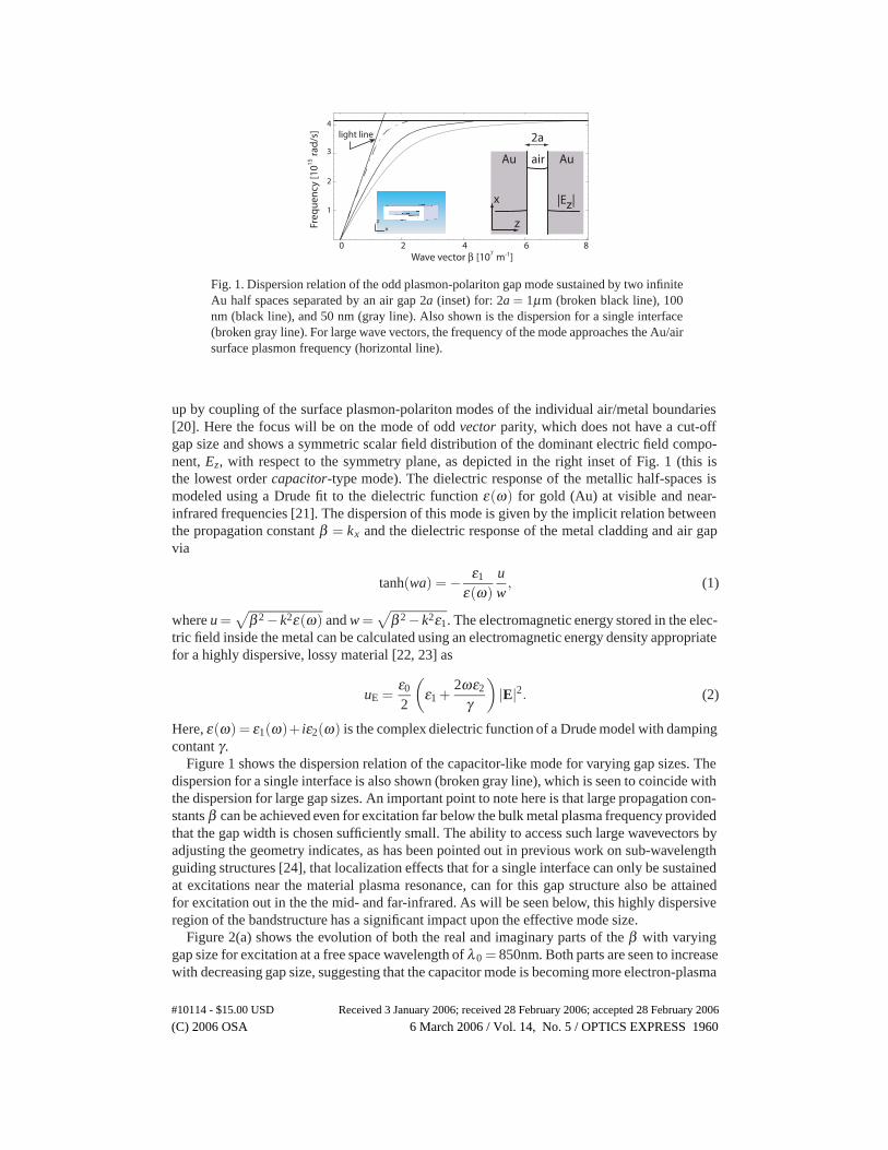
0 2 4 6 8
Freq
uen
cy [1
015 ra
d/s
]
2a
air AuAu
Wave vector β [107 m-1]
x
z
|Ez|
light line4
3
2
1
xz
Fig. 1. Dispersion relation of the odd plasmon-polariton gap mode sustained by two infiniteAu half spaces separated by an air gap 2a (inset) for: 2a = 1μm (broken black line), 100nm (black line), and 50 nm (gray line). Also shown is the dispersion for a single interface(broken gray line). For large wave vectors, the frequency of the mode approaches the Au/airsurface plasmon frequency (horizontal line).
up by coupling of the surface plasmon-polariton modes of the individual air/metal boundaries[20]. Here the focus will be on the mode of odd vector parity, which does not have a cut-offgap size and shows a symmetric scalar field distribution of the dominant electric field compo-nent, Ez, with respect to the symmetry plane, as depicted in the right inset of Fig. 1 (this isthe lowest order capacitor-type mode). The dielectric response of the metallic half-spaces ismodeled using a Drude fit to the dielectric function ε(ω) for gold (Au) at visible and near-infrared frequencies [21]. The dispersion of this mode is given by the implicit relation betweenthe propagation constant β = kx and the dielectric response of the metal cladding and air gapvia
tanh(wa) = − ε1
ε(ω)uw
, (1)
where u =√
β 2 − k2ε(ω) and w =√
β 2 − k2ε1. The electromagnetic energy stored in the elec-tric field inside the metal can be calculated using an electromagnetic energy density appropriatefor a highly dispersive, lossy material [22, 23] as
uE =ε0
2
(ε1 +
2ωε2
γ
)|E|2. (2)
Here, ε(ω) = ε1(ω)+ iε2(ω) is the complex dielectric function of a Drude model with dampingcontant γ .
Figure 1 shows the dispersion relation of the capacitor-like mode for varying gap sizes. Thedispersion for a single interface is also shown (broken gray line), which is seen to coincide withthe dispersion for large gap sizes. An important point to note here is that large propagation con-stants β can be achieved even for excitation far below the bulk metal plasma frequency providedthat the gap width is chosen sufficiently small. The ability to access such large wavevectors byadjusting the geometry indicates, as has been pointed out in previous work on sub-wavelengthguiding structures [24], that localization effects that for a single interface can only be sustainedat excitations near the material plasma resonance, can for this gap structure also be attainedfor excitation out in the the mid- and far-infrared. As will be seen below, this highly dispersiveregion of the bandstructure has a significant impact upon the effective mode size.
Figure 2(a) shows the evolution of both the real and imaginary parts of the β with varyinggap size for excitation at a free space wavelength of λ0 = 850nm. Both parts are seen to increasewith decreasing gap size, suggesting that the capacitor mode is becoming more electron-plasma
#10114 - $15.00 USD Received 3 January 2006; received 28 February 2006; accepted 28 February 2006
(C) 2006 OSA 6 March 2006 / Vol. 14, No. 5 / OPTICS EXPRESS 1960
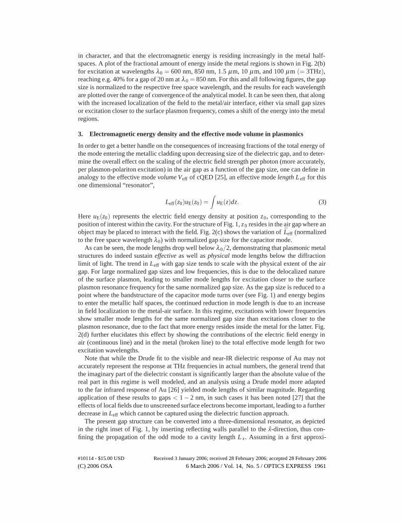
in character, and that the electromagnetic energy is residing increasingly in the metal half-spaces. A plot of the fractional amount of energy inside the metal regions is shown in Fig. 2(b)for excitation at wavelengths λ0 = 600 nm, 850 nm, 1.5 μm, 10 μm, and 100 μm (= 3THz),reaching e.g. 40% for a gap of 20 nm at λ 0 = 850 nm. For this and all following figures, the gapsize is normalized to the respective free space wavelength, and the results for each wavelengthare plotted over the range of convergence of the analytical model. It can be seen then, that alongwith the increased localization of the field to the metal/air interface, either via small gap sizesor excitation closer to the surface plasmon frequency, comes a shift of the energy into the metalregions.
3. Electromagnetic energy density and the effective mode volume in plasmonics
In order to get a better handle on the consequences of increasing fractions of the total energy ofthe mode entering the metallic cladding upon decreasing size of the dielectric gap, and to deter-mine the overall effect on the scaling of the electric field strength per photon (more accurately,per plasmon-polariton excitation) in the air gap as a function of the gap size, one can define inanalogy to the effective mode volume Veff of cQED [25], an effective mode length L eff for thisone dimensional “resonator”,
Leff(z0)uE(z0) =∫
uE(z)dz. (3)
Here uE(z0) represents the electric field energy density at position z0, corresponding to theposition of interest within the cavity. For the structure of Fig. 1, z 0 resides in the air gap where anobject may be placed to interact with the field. Fig. 2(c) shows the variation of Leff (normalizedto the free space wavelength λ0) with normalized gap size for the capacitor mode.
As can be seen, the mode lengths drop well below λ0/2, demonstrating that plasmonic metalstructures do indeed sustain effective as well as physical mode lengths below the diffractionlimit of light. The trend in Leff with gap size tends to scale with the physical extent of the airgap. For large normalized gap sizes and low frequencies, this is due to the delocalized natureof the surface plasmon, leading to smaller mode lengths for excitation closer to the surfaceplasmon resonance frequency for the same normalized gap size. As the gap size is reduced to apoint where the bandstructure of the capacitor mode turns over (see Fig. 1) and energy beginsto enter the metallic half spaces, the continued reduction in mode length is due to an increasein field localization to the metal-air surface. In this regime, excitations with lower frequenciesshow smaller mode lengths for the same normalized gap size than excitations closer to theplasmon resonance, due to the fact that more energy resides inside the metal for the latter. Fig.2(d) further elucidates this effect by showing the contributions of the electric field energy inair (continuous line) and in the metal (broken line) to the total effective mode length for twoexcitation wavelengths.
Note that while the Drude fit to the visible and near-IR dielectric response of Au may notaccurately represent the response at THz frequencies in actual numbers, the general trend thatthe imaginary part of the dielectric constant is significantly larger than the absolute value of thereal part in this regime is well modeled, and an analysis using a Drude model more adaptedto the far infrared response of Au [26] yielded mode lengths of similar magnitude. Regardingapplication of these results to gaps < 1− 2 nm, in such cases it has been noted [27] that theeffects of local fields due to unscreened surface electrons become important, leading to a furtherdecrease in Leff which cannot be captured using the dielectric function approach.
The present gap structure can be converted into a three-dimensional resonator, as depictedin the right inset of Fig. 1, by inserting reflecting walls parallel to the x-direction, thus con-fining the propagation of the odd mode to a cavity length L x. Assuming in a first approxi-
#10114 - $15.00 USD Received 3 January 2006; received 28 February 2006; accepted 28 February 2006
(C) 2006 OSA 6 March 2006 / Vol. 14, No. 5 / OPTICS EXPRESS 1961
0.01
0.1
1
10
10-2 110-4
normalized gap size
% e
ner
gy
in m
etal
0.1
1
Gap size 2a [nm]20 8010
β/k 0
2
Mo
de
Len
gth
, L ef
f
10-1
_10-2
10-3
10-4
(c)
(b)(a) 100
10-3 10-1 10
1
10
10-2 110-4
normalized gap size10-3 10-1 10
10-2 110-4
normalized gap size10-3 10-1 10
Mo
de
Len
gth
, L ef
f
10-1
10-2
10-3
10-4
(d) 1
_
Fig. 2. (a) Normalized propagation constant β versus gap size at λ0 = 850nm. Both thereal (solid curve) and the imaginary (broken curve, 10x) part of β are seen to increase fordecreasing gap. (b) Fractional electric field energy residing inside the metallic half spacesas a function of normalized gap size for excitation at λ0 = 600 nm (thick line), 850nm(black line), 1.5 μm (gray line), 10 μm (broken black line), and 100 μm (broken grayline). (c) Effective mode length Leff normalized to free space wavelength λ0. (d) Effectivemode length in the air gap (continuous line) and in the surrounding metal (broken line) forλ0 = 600 nm (black line) and 1.5 μm (gray line).
mation perfectly reflecting cavity walls, the fundamental cavity mode will be excited whenLx = π/β (λ0,a). If one conservatively assumes a diffraction-limited lateral resonator widthLy = λ0/2, the cavity mode volume can thus be approximated as Veff ∼ Leff(πλ0/2β ).
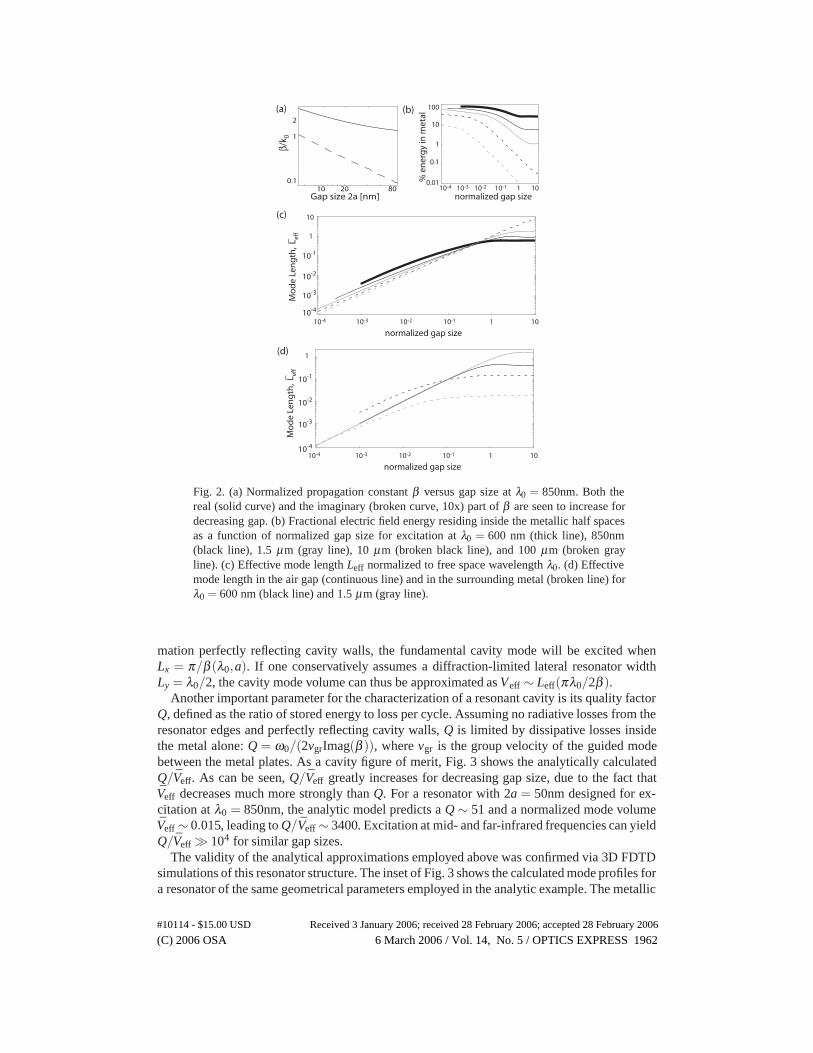
Another important parameter for the characterization of a resonant cavity is its quality factorQ, defined as the ratio of stored energy to loss per cycle. Assuming no radiative losses from theresonator edges and perfectly reflecting cavity walls, Q is limited by dissipative losses insidethe metal alone: Q = ω0/(2vgrImag(β )), where vgr is the group velocity of the guided modebetween the metal plates. As a cavity figure of merit, Fig. 3 shows the analytically calculatedQ/Veff. As can be seen, Q/Veff greatly increases for decreasing gap size, due to the fact thatVeff decreases much more strongly than Q. For a resonator with 2a = 50nm designed for ex-citation at λ0 = 850nm, the analytic model predicts a Q ∼ 51 and a normalized mode volumeVeff ∼ 0.015, leading to Q/Veff ∼ 3400. Excitation at mid- and far-infrared frequencies can yieldQ/Veff � 104 for similar gap sizes.
The validity of the analytical approximations employed above was confirmed via 3D FDTDsimulations of this resonator structure. The inset of Fig. 3 shows the calculated mode profiles fora resonator of the same geometrical parameters employed in the analytic example. The metallic
#10114 - $15.00 USD Received 3 January 2006; received 28 February 2006; accepted 28 February 2006
(C) 2006 OSA 6 March 2006 / Vol. 14, No. 5 / OPTICS EXPRESS 1962
Q/V
eff
x
z
y
x1 3 5 7 9
104
105
_
106
103
10-2 110-4
normalized gap size10-3 10-1 10
Fig. 3. Ratio of Q to Veff for a 3D gap resonator of varying normalized gap size for the fiveexcitation wavelengths of Fig. 2. The inset shows a FDTD calculated electric field intensityof a resonator with 2a = 50nm and λ0 = 980nm.
Au half-spaces were modeled with the same Drude function used in the analytic calculations;however, the reflecting mirror walls were in this case taken to be non-perfect, consisting alsoof Au. As a result, the resonance wavelength shifts from λ 0 = 850nm to 980nm due to theelectric field penetration into the end mirrors. The calculated absorptive Q abs ∼ 40 is of similarmagnitude as the analytic result, and a radiative Q rad ∼ 100 is found due to lateral leakageof radiation. The FDTD-calculated mode volume Veff ∼ 0.009 is also in good agreement withthe analytic model estimate when scaled by the cube of the increase in resonance wavelength.While these discussions have focused on a planar metal/insulator/metal heterostructure, thegeneral conclusions regarding Q/Veff are also expected to hold for more complicated geometriesinvolving two metallic surfaces separated by a nanoscale gap, such as e.g. nanoshells.
4. Application to surface-enhanced Raman scattering
One is now in a position to sketch as an example of the usefulness of the effective mode volumepicture to describe plasmonic energy localization its application to SERS. A spontaneous Ra-man scattering process involves an incoming excitation beam of intensity |E i(ω0)|2/2η (η theimpedance of free space) and frequency ω 0, leading to the emission of Stokes photons at fre-quency ω through a Raman active molecule. Due to the small Stokes emission shift, one usuallyassumes equal enhancement of the exciting field and the outgoing Stokes field, and a commonlyused expression[19] for the enhancement of the Raman cross section is R = |E loc|4/|Ei|4, where|Eloc| is the local field amplitude at the Raman active site. For this treatment, Q(ω0)=Q(ω)=Qand Veff(ω0)=Veff(ω)=Veff, and it is thus assumed that both the incoming and the emitted photonare resonant with the cavity.
With |s+|2 = |Ei|2Ai/2η being the power carried by the incident beam of cross section A i,the evolution of the on-resonance mode amplitude u inside the cavity can be calculated from[28], u(t) = − γ
2u(t)+ κs+, where u2 represents the total time-averaged energy in the cavity,γ = γrad + γabs is the energy decay rate due to radiation (γ rad) and absorption (γabs), and κ isthe coupling coefficient to external input which depends on the size and shape of the excitationbeam. κ can be expressed as κ =
√γi, where γi is the contribution of the excitation channel tothe total radiative decay rate [28]. For a symmetric two-sided cavity, in a first approximationone can estimate γi = (γrad/2)(Ac/Ai), with Ac corresponding to an effective radiation cross-section of the resonant cavity mode (its radiation field imaged back into the near-field of thecavity). Note that Ai has been assumed to be larger than Ac in the above relation, and that Ac
can be no smaller than the diffraction limited area Ad , yielding Ad ≤ Ac ≤ Ai. In steady state,
#10114 - $15.00 USD Received 3 January 2006; received 28 February 2006; accepted 28 February 2006
(C) 2006 OSA 6 March 2006 / Vol. 14, No. 5 / OPTICS EXPRESS 1963
the mode amplitude can then be expressed as
u =
√2γradAc/Ai|s+|γrad + γabs
=√
γradAc|Ei|√η(γrad + γabs)
, (4)
which for fixed incoming power is maximum upon spatial mode matching (A c = Ai). For adielectric cavity (γrad � γabs), one thus gets u ∝ 1/
√γrad ∝√
Q, while for a metallic cavity(γabs � γrad) u ∝ 1/γabs ∝ Q, explaining the different scaling laws for field enhancement indielectric [29] and metallic [30] resonators encountered in the literature. From the definitionof effective mode volume one can write the resonant mode amplitude as u =
√ε0|Eloc|
√Veff,
which gives for the enhancement of the incoming radiation in a metallic cavity
√R =
|Eloc|2|Ei|2 =
γradAc
4π2c2ηε0λ0
Q2
Veff. (5)
A similar scaling law has previously been obtained for plasmonic energy localization in fractal-like metal nanoparticle aggregates on metal surfaces [31]. Setting A c = Ad yields for our ex-ample Au resonator, with 2a = 50 nm and λ0 = 980 nm, an estimated SERS cross sectionenhancement of R ∼ 1600.
A similar estimate of R for a crevice between two Ag nanoparticles separated by a nanoscalegap, a configuration which is believed to sustain SERS hot-spots with R∼ 10 11 upon resonance,can also be obtained using the effective mode volume picture. The crevice can be approxi-mately modeled using the capacitor-like cavity described above, but with a reduced lateral widthLy ∼ Lx=π/β . For a 1 nm gap, with λ0 = 400nm, Ac=Ad , and (Q,γrad) estimated from FDTD,eq. (5) yields R ∼ 2.7×10¹⁰, in good agreement with full-field three-dimensional simulationsof the enhancement for this coupled particle geometry [6]. The total observable enhancementof the Stokes emission can be estimated as the product of the field enhancement of the incom-ing radiation and the enhanced radiative decay rate at the Stokes frequency. As is well known,a dipole oscillator placed inside a metallic cavity shows an increase in its total decay rateγ/γ0 = (3/4π2)(Q/Veff)[32]. For collection of light emission outside the cavity, the overall cav-ity enhancement is weighted with an extraction efficiency, Q/Q rad[33, 34]. Thus, the emissionenhancement at the peak emission frequency of the Stokes line is (3/4π 2)(Q2/Veff)(Q/Qrad).Incorporating the relation for incoming field enhancement from eq. (5), the overall enhance-ment is estimated to be 1.5×10¹² for the crevice example, similar to observed values[5, 4].
5. Conclusion
The description of controlled spatial electromagnetic energy localization via an effective modevolume - traditionally applied to (non-dispersive) dielectric resonators - has been extended tometallic cavities sustaining surface plasmon-polaritons and applied to the description of SERS.Using a simple model of a nanoscale plasmonic resonator with a realistic material dielectricresponse function, it has been demonstrated that plasmonic cavities can indeed confine electro-magnetic energy into both physical and effective mode volumes far below the diffraction limit.Large Q/Veff values can be achieved for nanometric gap sizes in metal/dielectric/metal het-erostructures. Furthermore, the field enhancement due to interactions between closely spacedmetallic interfaces of more complicated geometries such as nanoparticles can be estimated inthese terms. This unified description of enhancement effects in both dielectric and metallicresonators will help in establishing new design principles for nanophotonic devices.
Acknowledgments
Thanks are expressed to Oskar Painter for stimulating discussions. This work was in part fundedby the UK Engineering and Physical Sciences Research Council (EPSRC).
#10114 - $15.00 USD Received 3 January 2006; received 28 February 2006; accepted 28 February 2006
(C) 2006 OSA 6 March 2006 / Vol. 14, No. 5 / OPTICS EXPRESS 1964

![Rapid determination of plasmonic nanoparticle agglomeration ......Surface enhanced Raman spectroscopy (SERS) has been used to identifycirculating tumor cells in blood [40] and detect](https://img.pdfslide.us/doc/110x75/604fcfc19bdc5911ab5110d7/rapid-determination-of-plasmonic-nanoparticle-agglomeration-surface-enhanced.jpg)