Embed Size (px)
Citation preview
HAL Id: hal-02549034https://hal.archives-ouvertes.fr/hal-02549034
Submitted on 21 Apr 2020
HAL is a multi-disciplinary open accessarchive for the deposit and dissemination of sci-entific research documents, whether they are pub-lished or not. The documents may come fromteaching and research institutions in France orabroad, or from public or private research centers.
L’archive ouverte pluridisciplinaire HAL, estdestinée au dépôt et à la diffusion de documentsscientifiques de niveau recherche, publiés ou non,émanant des établissements d’enseignement et derecherche français ou étrangers, des laboratoirespublics ou privés.
Plasma-digital nexus: plasma nanotechnology for thedigital manufacturing age
J. Hong, A. Murphy, B. Ashford, P. Cullen, T. Belmonte, K. Ostrikov
To cite this version:J. Hong, A. Murphy, B. Ashford, P. Cullen, T. Belmonte, et al.. Plasma-digital nexus: plasmananotechnology for the digital manufacturing age. Reviews of Modern Plasma Physics, SpringerSingapore, 2020, 4 (1), �10.1007/s41614-019-0039-8�. �hal-02549034�
1
Plasma-digital nexus: plasma nanotechnology
for digital manufacturing age
J. Hong1, A. B. Murphy1, B. Ashford1, P. J. Cullen2, T. Belmonte3, and K. Ostrikov4
1 CSIRO Manufacturing, PO Box 218, Lindfield NSW 2070, Australia 2 School of Chemical and Biomolecular Engineering, The University of Sydney, Sydney NSW 2007, Australia 3 Université de Lorraine, Institut Jean Lamour, UMR CNRS 7198, Nancy, France 4 School of Chemistry, Physics and Mechanical Engineering, Queensland University of Technology, Brisbane
QLD 4001, Australia
Abstract: Digital transformation in manufacturing is one of the key megatrends in the development of
global economy and society. Three-dimensional (3D) printing is a transformative digital technology
poised to disrupt manufacturing and supply chains across major industries. Here we critically examine
relevant insights into current and emerging applications of plasma nanotechnology in printing, including
3D printing. Plasma devices operated at atmospheric pressure coupled with printing processes may help
strengthen 3D printing as an emerging fabrication technology that morphs diverse metal powders,
polymers, plastics and other materials into digitally designed 3D shapes and patterns. We discuss how
plasma applications may help overcome current limitations of 3D printing in various fields, e.g.
limitations of sculpting composite materials, lack of mechanical strength and the need for post-
processing. Our key focus is on the challenges, opportunities and physical mechanisms of the use of 3D
printing in nano-manufacturing, defined as the fabrication of nanoscale building blocks, such as
nanoparticles and nanomaterials; their assembly into higher-order (micro-scale) structures; and the
integration of these structures into larger (macro-) scale devices and systems by controlling energy and
matter at nanoscale. Moreover, we discuss the physico-chemical mechanisms that result in highly-
conformal deposition of nanostructured materials onto 3D surfaces with microscopic (and possibly
nanoscale) control of textures and inter-layer cross-linking, without the need for additional heating. We
further highlight the arising opportunities for plasma nanotechnology to synergize with the emerging
digital transformation platforms in surface micro- and nano-structuring using polymers, metals, metallic
alloys, and other materials. These new findings in plasma-digital nanoscale fabrication may lead to a
new digital manufacturing platform suitable for a number of cutting-edge applications in electronic,
sensing and energy devices.
Keywords: Plasma printing, Plasma nanotechnology, Additive manufacturing, Digital technologies
2
1. Introduction
1.1. Digital manufacturing age
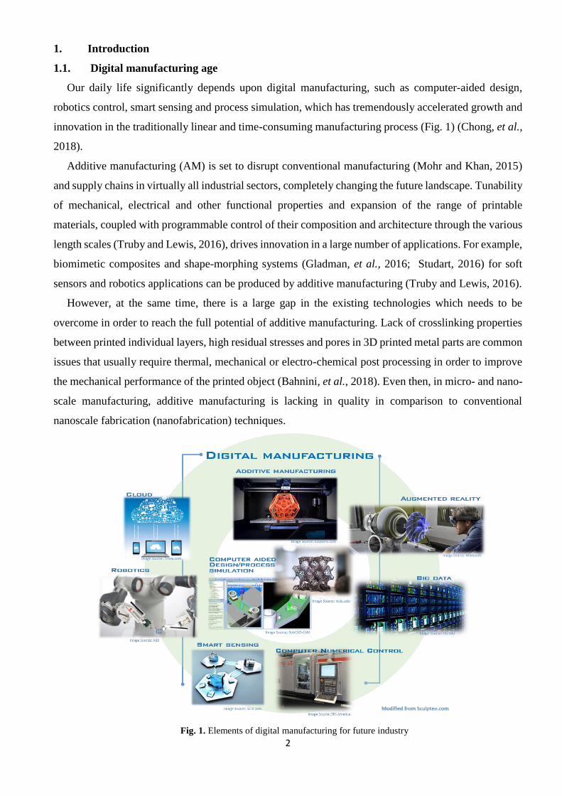
Our daily life significantly depends upon digital manufacturing, such as computer-aided design,
robotics control, smart sensing and process simulation, which has tremendously accelerated growth and
innovation in the traditionally linear and time-consuming manufacturing process (Fig. 1) (Chong, et al.,
2018).
Additive manufacturing (AM) is set to disrupt conventional manufacturing (Mohr and Khan, 2015)
and supply chains in virtually all industrial sectors, completely changing the future landscape. Tunability
of mechanical, electrical and other functional properties and expansion of the range of printable
materials, coupled with programmable control of their composition and architecture through the various
length scales (Truby and Lewis, 2016), drives innovation in a large number of applications. For example,
biomimetic composites and shape-morphing systems (Gladman, et al., 2016; Studart, 2016) for soft
sensors and robotics applications can be produced by additive manufacturing (Truby and Lewis, 2016).
However, at the same time, there is a large gap in the existing technologies which needs to be
overcome in order to reach the full potential of additive manufacturing. Lack of crosslinking properties
between printed individual layers, high residual stresses and pores in 3D printed metal parts are common
issues that usually require thermal, mechanical or electro-chemical post processing in order to improve
the mechanical performance of the printed object (Bahnini, et al., 2018). Even then, in micro- and nano-
scale manufacturing, additive manufacturing is lacking in quality in comparison to conventional
nanoscale fabrication (nanofabrication) techniques.
Fig. 1. Elements of digital manufacturing for future industry
3
In order to overcome the current limits of 3D printing technologies and meet the inspiring goal of
creating architected matter that has qualitatively new properties with unprecedented control over the
material’s composition, structure, function and dynamics (Hirt, et al., 2017), more effective control
factors are required. Potentially, low-temperature plasmas may provide a solution to these issues.
Plasma has played a significant role in enabling the innovation of current high-end manufacturing
processes, such as in semiconductor and display industries. Precisely controlled physical/chemical
reactions involving high density electrons, energetic ionic species and various chemically reactive
neutral radicals have made plasma an indispensable tool to the microelectronics industry, where one
third of the manufacturing steps of microelectronic circuits and microprocessors are plasma-based
(d'Agostino, et al., 2005). In addition, due to the wide range of plasma characteristics – from the high-
temperature, high-energy application of nuclear fusion processes to low temperature atmospheric-
pressure surface modification – plasma technologies have shaped everyday lives through the numerous
manufacturing processes they are employed in (John, 2005; Weltmann, et al., 2019).
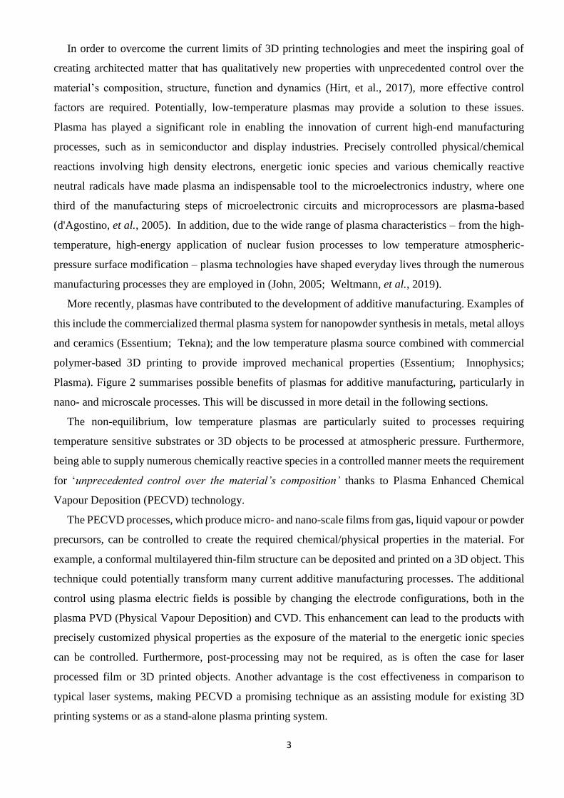
More recently, plasmas have contributed to the development of additive manufacturing. Examples of
this include the commercialized thermal plasma system for nanopowder synthesis in metals, metal alloys
and ceramics (Essentium; Tekna); and the low temperature plasma source combined with commercial
polymer-based 3D printing to provide improved mechanical properties (Essentium; Innophysics;
Plasma). Figure 2 summarises possible benefits of plasmas for additive manufacturing, particularly in
nano- and microscale processes. This will be discussed in more detail in the following sections.
The non-equilibrium, low temperature plasmas are particularly suited to processes requiring
temperature sensitive substrates or 3D objects to be processed at atmospheric pressure. Furthermore,
being able to supply numerous chemically reactive species in a controlled manner meets the requirement
for ‘unprecedented control over the material’s composition’ thanks to Plasma Enhanced Chemical
Vapour Deposition (PECVD) technology.
The PECVD processes, which produce micro- and nano-scale films from gas, liquid vapour or powder
precursors, can be controlled to create the required chemical/physical properties in the material. For
example, a conformal multilayered thin-film structure can be deposited and printed on a 3D object. This
technique could potentially transform many current additive manufacturing processes. The additional
control using plasma electric fields is possible by changing the electrode configurations, both in the
plasma PVD (Physical Vapour Deposition) and CVD. This enhancement can lead to the products with
precisely customized physical properties as the exposure of the material to the energetic ionic species
can be controlled. Furthermore, post-processing may not be required, as is often the case for laser
processed film or 3D printed objects. Another advantage is the cost effectiveness in comparison to
typical laser systems, making PECVD a promising technique as an assisting module for existing 3D
printing systems or as a stand-alone plasma printing system.
4
In the following, we will discuss some of the recent developments in the digital manufacturing and
critically examine the areas where the use of plasmas may contribute to the future development of this
rapidly emerging technological field.
Fig. 2 Possible benefits of plasma processes for additive manufacturing
1.2. Printing and plasma: a synergy for digital manufacturing
The idea of adapting plasma technology for the printing process was proposed in early 2000s.
Microplasmas using a dielectric barrier sandwiched between two electrodes enabled precise gravure
printing with the 50-70 µm linewidth (Fig. 3) (Thomas, et al., 2012). Using this technique, a desired
pattern can be engraved in the conductive electrode surface or dielectric layer. It can further support
Roll-to-Roll (R2R) continuous plasma processing on a flexible polymer film. The focus has mainly been
towards surface modification to enhance hydrophilicity prior to the actual printing process. Using C2H2
mixed as a reactive gas, the ‘plasma stamping’ technique has been demonstrated to deposit a patterned
polymer film with the minimum linewidth of 50 µm. However, the thickness of the printed layer was
not uniform due to the inhomogeneous nature of the porous metal electrode through which the gas was
transported.
Fig. 3 (a) Printer roller showing the engraved pattern, (b) plasma printed and subsequently electroless copper metallized
model structure with a line width as low as 70 μm, (c) plasma printed grid of an amorphous hydrogenated carbon film,
obtained from 1% C2H2 in He, using a porous sinter metal electrode to provide gas supply and (d) schematic of plasma
printing with gas-fed microplasmas using an electrode made from sintered metal powder. Vertical arrows indicate the gas
flow (Thomas, et al., 2012)
5
Significant efforts have been made to create flexible printing methods using atmospheric pressure
plasmas without the limitations associated with fixed pattern or electrode configuration. Recently, as the
growth of additive manufacturing has accelerated, the contribution from the plasma technology has also
increased. Plasma printing of multiwalled carbon nanotubes was demonstrated on paper substrates using
an atmospheric pressure plasma jet (Gandhiraman, et al., 2016). The plasma-printed carbon nanotubes
showed denser morphology and higher conductivity in comparison to non-plasma processed samples.
The printed nanotubes showed good performance for a dopamine and ammonia sensing. The same group
also reported the plasma jet printing and in situ reduction of graphene oxide (Dey, et al., 2018) using
He/H2 gas, thus revealing the possibility to control chemical properties through the use of plasmas. This
approach enabled removal of the multiple intermediate steps of chemical reduction and washing which
are usually required to increase the conductivity of graphene oxide films.
Another significant advantage of using plasmas is the enhanced mechanical properties resulting from
the improved chemical bond strength. It was shown that plasma can ‘weld’ different sheets of porous
3D graphene scaffolds to create strong intermolecular bonding (Chakravarty, et al., 2016). The plasma
welded scaffolds (Fig. 4) were produced to maintain a high porosity and ultra-low density with an
interconnected, layered, open microstructure which had high yield strength and stiffness values
(Chakravarty, et al., 2016).
Fig. 4 (Left) Schematic representing the stacking of 2D graphene sheet (Right) (a) SEM image of the top surface of graphene
sample at different magnifications (digital image and SEM image at low magnification as insets) (b) Bright field transmission
electron microscopy image of graphene oxide showing randomly oriented sheets welded together (top left inset shows two
sheets welded at the edge; inset at the bottom on right shows HRTEM image of the welded region) (c) Bright field TEM
image of side-edge-welded graphene sheets, HRTEM image of the welded region showing defect, and FFT of the region
showing misorientation of the two sheets; the line in inset corresponds to 0.5 nm distance and d) 50° tilted SEM image of the
3D architecture of the plasma welded sample by SPS (spark plasma sintering) technique observed after FIB at the center of
the sample (shown as inset) (Chakravarty, et al., 2016)
Researchers at the Fraunhofer Institute presented a 3D printing system combined with the plasma
coating unit for bone implants (Fig. 5) (Fraunhofer, 2018). Using a plasma jet, it was possible to fabricate
a cell growth-promoting coating functionalized with amino groups and apply these coatings to the
interior and exterior surfaces of the implants.
6
Fig. 5. (a) Plasma-jet coating of medical implant scaffolds (b) Schematic shows how to manufacture coated scaffolds:
immediately after extrusion, the scaffold structures are treated with a cold plasma (Image source: Fraunhofer IST)
In recent years, there have appeared a few commercial 3D printer products which have been given
the name ‘plasma printer’ as shown in Fig. 6. These printers are equipped with an additional plasma
module for surface modification, welding and plasma assisted deposition of metal oxide film. These
printers represent a promising platform to fabricate functionalized device elements by surface coating,
scribing or etching of single/multiple layers and detailed discussion will be provided in section 5.1 and
5.3.
Fig. 6 Examples of commercial plasma printers. Image Sources (from left to right): Relyon Plasma, Essentium3d and
Innophysics
To identify where and how plasma technology can potentially benefit the existing and future digital
manufacturing platforms, we will first overview the selected current manufacturing processes.
2. Representative printing technologies
2.1 2D printing
To obtain a better insight on printing technology it is worthwhile to review some of the common 2D
printing processes as a comparison to 3D manufacturing. Lithography is a common method for obtaining
a pattern in layers. This technology helped establish modern microelectronics based industry and
emerging internet of things (IoT) technologies. However, we will focus on conventional printing which
can produce written patterns. Fig. 7 shows schematics of some examples of printing technology on a flat
substrate: screen printing, gravure printing, inkjet printing and high-resolution electrohydrodynamic jet
7
printing (Park, et al., 2007). As shown in Fig. 7 (a), in the screen printing process, the ink transfers
through the patterned mesh onto a substrate by squeegee. In gravure printing, a pattern is etched onto a
metal cylinder. The paper (or another substrate) is pressed against the inked cylinder on a rotary press,
transferring the image directly to the substrate. Although the resolution of screen printing and gravure
printing prevents these techniques from producing high-end products, they are still widely used
techniques and the possibility of adapting plasma treatment to improve the printing quality through the
increased wetting and adhesion properties has been explored.
Aside from the conventional office and household uses, inkjet printing has been widely used as an
effective tool for the fabrication of flexible electronics, optical and photonic devices and more (Alaman,
et al., 2016). This is because of the attractive features of inkjet printing that support the additive
operation. Indeed, this technique is able to pattern directly regardless of the type of substrates, even on
biological materials that are incompatible with the established patterning methods such as
photolithography. Further benefits of inkjet printing include the flexibility in structural design due to
software-based control, compatibility with large-area substrates, and the potential for low-cost operation
(de Gans, et al., 2004; Forrest, 2004; Parashkov, et al., 2005; Park, et al., 2007). Inkjet printing is able
to process not only organic materials, but also conductive inks such as metal nanoparticles (Magdassi,
et al., 2003; Lee, et al., 2005), single-wall/multi-wall carbon nanotubes (SWCNTs/MWCNTs) (Wei, et
al., 2007; Mabrook, et al., 2009) and graphene (Wang, et al., 2016a).
Fig. 7. Schematics showing working principle of (a) Screen printing (EMPA) (b) Gravure printing (EMPA) (c) inkjet
printing (Xu, et al., 2007) and (d) electrohydrodynamic printing where PEGDA indicates poly(ethylene glycol) diacrylate
as an example of a printable material (Corbin, et al., 2013)
However, the minimum achievable linewidth is typically in the range of 20–30 µm (Szczech, et al.,
2002; Ling and Bao, 2004; Sanaur, et al., 2006) due to the large droplet diameters of ∼10–20 µm with
the placement errors typically ±10 µm (Sirringhaus, et al., 2000; Cheng, et al., 2005). In order to
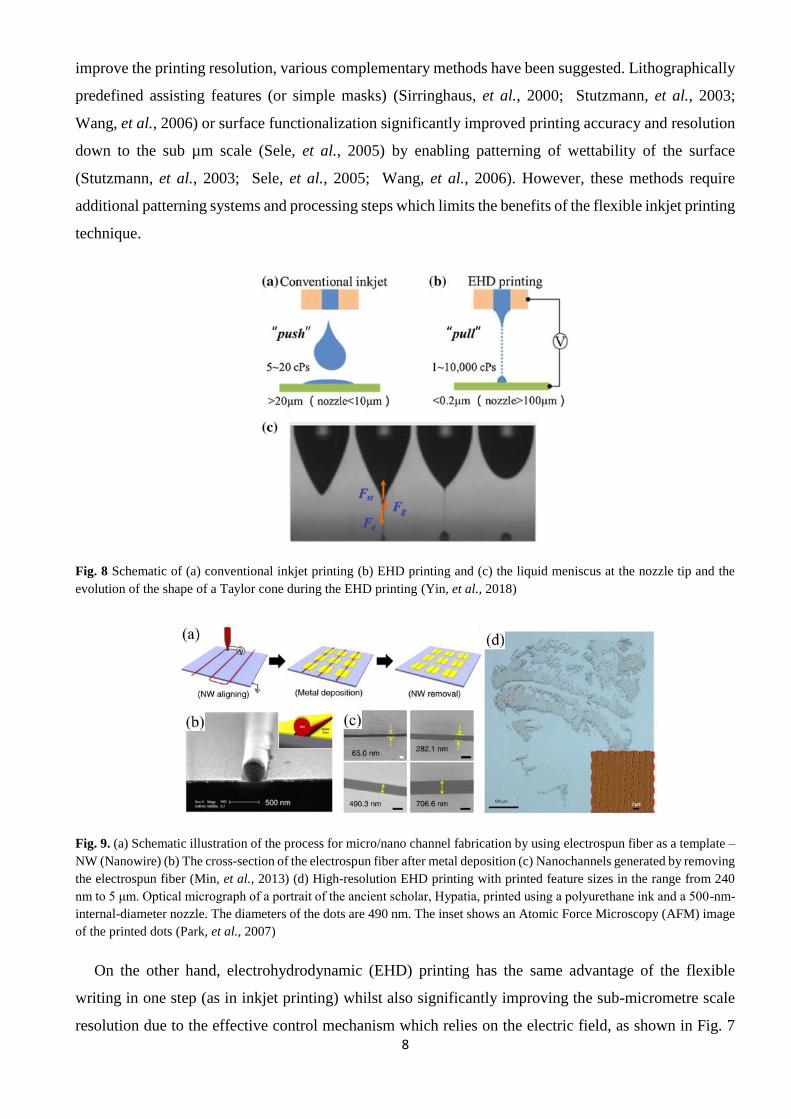
8
improve the printing resolution, various complementary methods have been suggested. Lithographically
predefined assisting features (or simple masks) (Sirringhaus, et al., 2000; Stutzmann, et al., 2003;
Wang, et al., 2006) or surface functionalization significantly improved printing accuracy and resolution
down to the sub µm scale (Sele, et al., 2005) by enabling patterning of wettability of the surface
(Stutzmann, et al., 2003; Sele, et al., 2005; Wang, et al., 2006). However, these methods require
additional patterning systems and processing steps which limits the benefits of the flexible inkjet printing
technique.
Fig. 8 Schematic of (a) conventional inkjet printing (b) EHD printing and (c) the liquid meniscus at the nozzle tip and the
evolution of the shape of a Taylor cone during the EHD printing (Yin, et al., 2018)
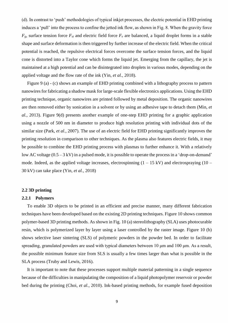
Fig. 9. (a) Schematic illustration of the process for micro/nano channel fabrication by using electrospun fiber as a template –
NW (Nanowire) (b) The cross-section of the electrospun fiber after metal deposition (c) Nanochannels generated by removing
the electrospun fiber (Min, et al., 2013) (d) High-resolution EHD printing with printed feature sizes in the range from 240
nm to 5 μm. Optical micrograph of a portrait of the ancient scholar, Hypatia, printed using a polyurethane ink and a 500-nm-
internal-diameter nozzle. The diameters of the dots are 490 nm. The inset shows an Atomic Force Microscopy (AFM) image
of the printed dots (Park, et al., 2007)
On the other hand, electrohydrodynamic (EHD) printing has the same advantage of the flexible
writing in one step (as in inkjet printing) whilst also significantly improving the sub-micrometre scale
resolution due to the effective control mechanism which relies on the electric field, as shown in Fig. 7
9
(d). In contrast to ‘push’ methodologies of typical inkjet processes, the electric potential in EHD printing
induces a ‘pull’ into the process to confine the jetted ink flow, as shown in Fig. 8. When the gravity force
Fg, surface tension force Fst and electric field force Fe are balanced, a liquid droplet forms in a stable
shape and surface deformation is then triggered by further increase of the electric field. When the critical
potential is reached, the repulsive electrical forces overcome the surface tension forces, and the liquid
cone is distorted into a Taylor cone which forms the liquid jet. Emerging from the capillary, the jet is
maintained at a high potential and can be disintegrated into droplets in various modes, depending on the
applied voltage and the flow rate of the ink (Yin, et al., 2018).
Figure 9 (a) - (c) shows an example of EHD printing combined with a lithography process to pattern
nanowires for fabricating a shadow mask for large-scale flexible electronics applications. Using the EHD
printing technique, organic nanowires are printed followed by metal deposition. The organic nanowires
are then removed either by sonication in a solvent or by using an adhesive tape to detach them (Min, et
al., 2013). Figure 9(d) presents another example of one-step EHD printing for a graphic application
using a nozzle of 500 nm in diameter to produce high resolution printing with individual dots of the
similar size (Park, et al., 2007). The use of an electric field for EHD printing significantly improves the
printing resolution in comparison to other techniques. As the plasma also features electric fields, it may
be possible to combine the EHD printing process with plasmas to further enhance it. With a relatively
low AC voltage (0.5 – 3 kV) in a pulsed mode, it is possible to operate the process in a ‘drop-on-demand’
mode. Indeed, as the applied voltage increases, electrospinning (1 – 15 kV) and electrospraying (10 –
30 kV) can take place (Yin, et al., 2018)
2.2 3D printing
2.2.1 Polymers
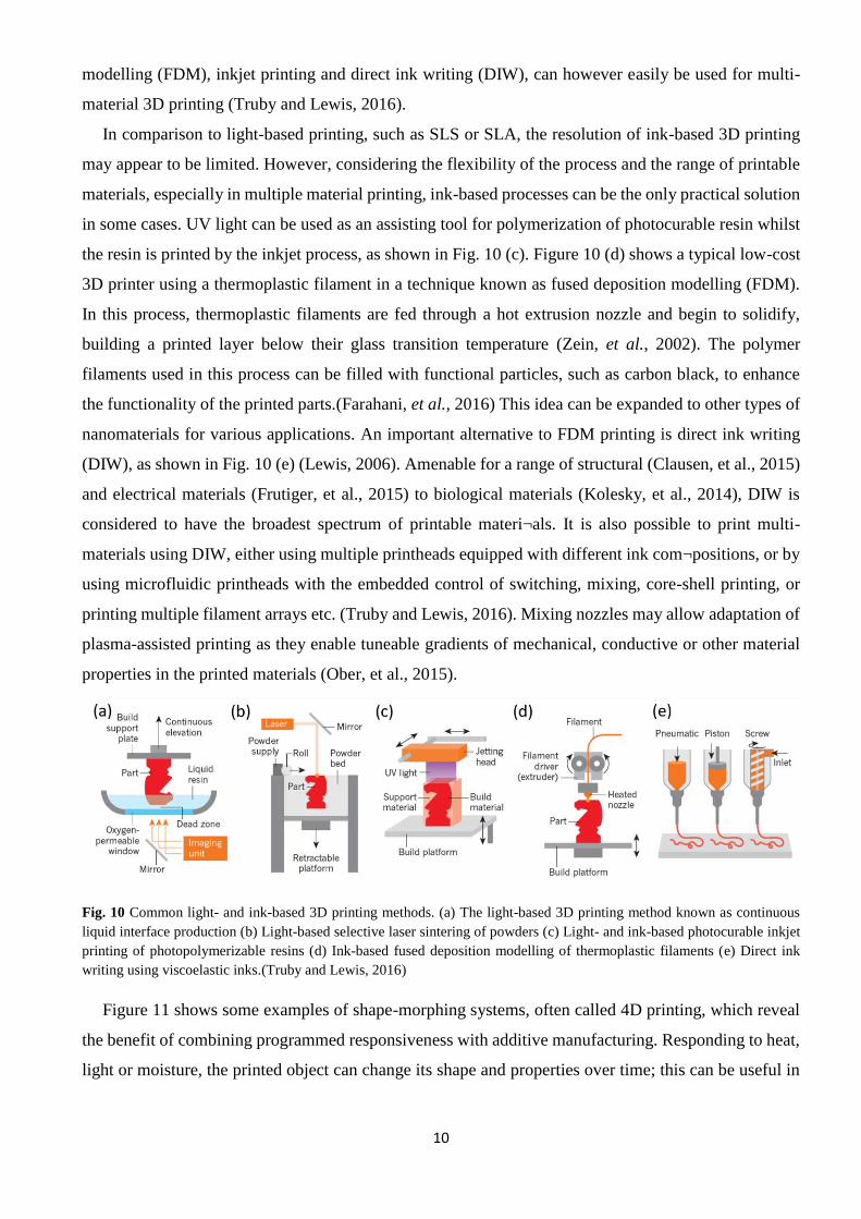
To enable 3D objects to be printed in an efficient and precise manner, many different fabrication
techniques have been developed based on the existing 2D printing techniques. Figure 10 shows common
polymer-based 3D printing methods. As shown in Fig. 10 (a) stereolithography (SLA) uses photocurable
resin, which is polymerized layer by layer using a laser controlled by the raster image. Figure 10 (b)
shows selective laser sintering (SLS) of polymeric powders in the powder bed. In order to facilitate
spreading, granulated powders are used with typical diameters between 10 μm and 100 μm. As a result,
the possible minimum feature size from SLS is usually a few times larger than what is possible in the
SLA process (Truby and Lewis, 2016).
It is important to note that these processes support multiple material patterning in a single sequence
because of the difficulties in manipulating the composition of a liquid photopolymer reservoir or powder
bed during the printing (Choi, et al., 2010). Ink-based printing methods, for example fused deposition
10
modelling (FDM), inkjet printing and direct ink writing (DIW), can however easily be used for multi-
material 3D printing (Truby and Lewis, 2016).
In comparison to light-based printing, such as SLS or SLA, the resolution of ink-based 3D printing
may appear to be limited. However, considering the flexibility of the process and the range of printable
materials, especially in multiple material printing, ink-based processes can be the only practical solution
in some cases. UV light can be used as an assisting tool for polymerization of photocurable resin whilst
the resin is printed by the inkjet process, as shown in Fig. 10 (c). Figure 10 (d) shows a typical low-cost
3D printer using a thermoplastic filament in a technique known as fused deposition modelling (FDM).
In this process, thermoplastic filaments are fed through a hot extrusion nozzle and begin to solidify,
building a printed layer below their glass transition temperature (Zein, et al., 2002). The polymer
filaments used in this process can be filled with functional particles, such as carbon black, to enhance
the functionality of the printed parts.(Farahani, et al., 2016) This idea can be expanded to other types of
nanomaterials for various applications. An important alternative to FDM printing is direct ink writing
(DIW), as shown in Fig. 10 (e) (Lewis, 2006). Amenable for a range of structural (Clausen, et al., 2015)
and electrical materials (Frutiger, et al., 2015) to biological materials (Kolesky, et al., 2014), DIW is
considered to have the broadest spectrum of printable materi¬als. It is also possible to print multi-
materials using DIW, either using multiple printheads equipped with different ink com¬positions, or by
using microfluidic printheads with the embedded control of switching, mixing, core-shell printing, or
printing multiple filament arrays etc. (Truby and Lewis, 2016). Mixing nozzles may allow adaptation of
plasma-assisted printing as they enable tuneable gradients of mechanical, conductive or other material
properties in the printed materials (Ober, et al., 2015).
Fig. 10 Common light- and ink-based 3D printing methods. (a) The light-based 3D printing method known as continuous
liquid interface production (b) Light-based selective laser sintering of powders (c) Light- and ink-based photocurable inkjet
printing of photopolymerizable resins (d) Ink-based fused deposition modelling of thermoplastic filaments (e) Direct ink
writing using viscoelastic inks.(Truby and Lewis, 2016)
Figure 11 shows some examples of shape-morphing systems, often called 4D printing, which reveal
the benefit of combining programmed responsiveness with additive manufacturing. Responding to heat,
light or moisture, the printed object can change its shape and properties over time; this can be useful in
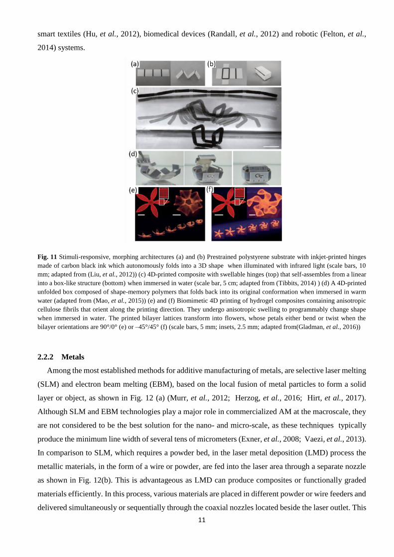
11
smart textiles (Hu, et al., 2012), biomedical devices (Randall, et al., 2012) and robotic (Felton, et al.,
2014) systems.
Fig. 11 Stimuli-responsive, morphing architectures (a) and (b) Prestrained polystyrene substrate with inkjet-printed hinges
made of carbon black ink which autonomously folds into a 3D shape when illuminated with infrared light (scale bars, 10
mm; adapted from (Liu, et al., 2012)) (c) 4D-printed composite with swellable hinges (top) that self-assembles from a linear
into a box-like structure (bottom) when immersed in water (scale bar, 5 cm; adapted from (Tibbits, 2014) ) (d) A 4D-printed
unfolded box composed of shape-memory polymers that folds back into its original conformation when immersed in warm
water (adapted from (Mao, et al., 2015)) (e) and (f) Biomimetic 4D printing of hydrogel composites containing anisotropic
cellulose fibrils that orient along the printing direction. They undergo anisotropic swelling to programmably change shape
when immersed in water. The printed bilayer lattices transform into flowers, whose petals either bend or twist when the
bilayer orientations are 90°/0° (e) or –45°/45° (f) (scale bars, 5 mm; insets, 2.5 mm; adapted from(Gladman, et al., 2016))
2.2.2 Metals
Among the most established methods for additive manufacturing of metals, are selective laser melting
(SLM) and electron beam melting (EBM), based on the local fusion of metal particles to form a solid
layer or object, as shown in Fig. 12 (a) (Murr, et al., 2012; Herzog, et al., 2016; Hirt, et al., 2017).
Although SLM and EBM technologies play a major role in commercialized AM at the macroscale, they
are not considered to be the best solution for the nano- and micro-scale, as these techniques typically
produce the minimum line width of several tens of micrometers (Exner, et al., 2008; Vaezi, et al., 2013).
In comparison to SLM, which requires a powder bed, in the laser metal deposition (LMD) process the
metallic materials, in the form of a wire or powder, are fed into the laser area through a separate nozzle
as shown in Fig. 12(b). This is advantageous as LMD can produce composites or functionally graded
materials efficiently. In this process, various materials are placed in different powder or wire feeders and
delivered simultaneously or sequentially through the coaxial nozzles located beside the laser outlet. This
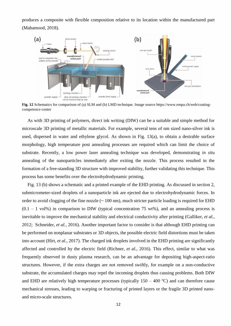
12
produces a composite with flexible composition relative to its location within the manufactured part
(Mahamood, 2018).
Fig. 12 Schematics for comparison of (a) SLM and (b) LMD technique. Image source https://www.empa.ch/web/coating-
competence-center
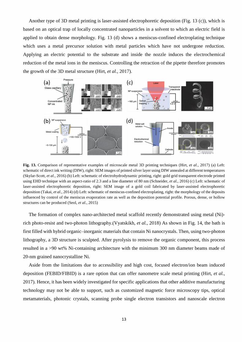
As with 3D printing of polymers, direct ink writing (DIW) can be a suitable and simple method for
microscale 3D printing of metallic materials. For example, several tens of nm sized nano-silver ink is
used, dispersed in water and ethylene glycol. As shown in Fig. 13(a), to obtain a desirable surface
morphology, high temperature post annealing processes are required which can limit the choice of
substrate. Recently, a low power laser annealing technique was developed, demonstrating in situ
annealing of the nanoparticles immediately after exiting the nozzle. This process resulted in the
formation of a free-standing 3D structure with improved stability, further validating this technique. This
process has some benefits over the electrohydrodynamic printing.
Fig. 13 (b) shows a schematic and a printed example of the EHD printing. As discussed in section 2,
submicrometer-sized droplets of a nanoparticle ink are ejected due to electrohydrodynamic forces. In
order to avoid clogging of the fine nozzle (~ 100 nm), much stricter particle loading is required for EHD
(0.1 – 1 vol%) in comparison to DIW (typical concentration 75 wt%), and an annealing process is
inevitable to improve the mechanical stability and electrical conductivity after printing (Galliker, et al.,
2012; Schneider, et al., 2016). Another important factor to consider is that although EHD printing can
be performed on nonplanar substrates or 3D objects, the possible electric field distortions must be taken
into account (Hirt, et al., 2017). The charged ink droplets involved in the EHD printing are significantly
affected and controlled by the electric field (Richner, et al., 2016). This effect, similar to what was
frequently observed in dusty plasma research, can be an advantage for depositing high-aspect-ratio
structures. However, if the extra charges are not removed swiftly, for example on a non-conductive
substrate, the accumulated charges may repel the incoming droplets thus causing problems. Both DIW
and EHD are relatively high temperature processes (typically 150 – 400 oC) and can therefore cause
mechanical stresses, leading to warping or fracturing of printed layers or the fragile 3D printed nano-
and micro-scale structures.
13
Another type of 3D metal printing is laser-assisted electrophoretic deposition (Fig. 13 (c)), which is
based on an optical trap of locally concentrated nanoparticles in a solvent to which an electric field is
applied to obtain dense morphology. Fig. 13 (d) shows a meniscus-confined electroplating technique
which uses a metal precursor solution with metal particles which have not undergone reduction.
Applying an electric potential to the substrate and inside the nozzle induces the electrochemical
reduction of the metal ions in the meniscus. Controlling the retraction of the pipette therefore promotes
the growth of the 3D metal structure (Hirt, et al., 2017).
Fig. 13. Comparison of representative examples of microscale metal 3D printing techniques (Hirt, et al., 2017) (a) Left:
schematic of direct ink writing (DIW), right: SEM images of printed silver layer using DIW annealed at different temperatures
(Skylar-Scott, et al., 2016) (b) Left: schematic of electrohydrodynamic printing, right: gold grid transparent electrode printed
using EHD technique with an aspect-ratio of 2.3 and a line diameter of 80 nm (Schneider, et al., 2016) (c) Left: schematic of
laser-assisted electrophoretic deposition, right: SEM image of a gold coil fabricated by laser-assisted electrophoretic
deposition (Takai, et al., 2014) (d) Left: schematic of meniscus-confined electroplating, right: the morphology of the deposits
influenced by control of the meniscus evaporation rate as well as the deposition potential profile. Porous, dense, or hollow
structures can be produced (Seol, et al., 2015)
The formation of complex nano-architected metal scaffold recently demonstrated using metal (Ni)-
rich photo-resist and two-photon lithography.(Vyatskikh, et al., 2018) As shown in Fig. 14, the bath is
first filled with hybrid organic–inorganic materials that contain Ni nanocrystals. Then, using two-photon
lithography, a 3D structure is sculpted. After pyrolysis to remove the organic component, this process
resulted in a >90 wt% Ni-containing architecture with the minimum 300 nm diameter beams made of
20-nm grained nanocrystalline Ni.
Aside from the limitations due to accessibility and high cost, focused electron/ion beam induced
deposition (FEBID/FIBID) is a rare option that can offer nanometre scale metal printing (Hirt, et al.,
2017). Hence, it has been widely investigated for specific applications that other additive manufacturing
technology may not be able to support, such as customized magnetic force microscopy tips, optical
metamaterials, photonic crystals, scanning probe single electron transistors and nanoscale electron
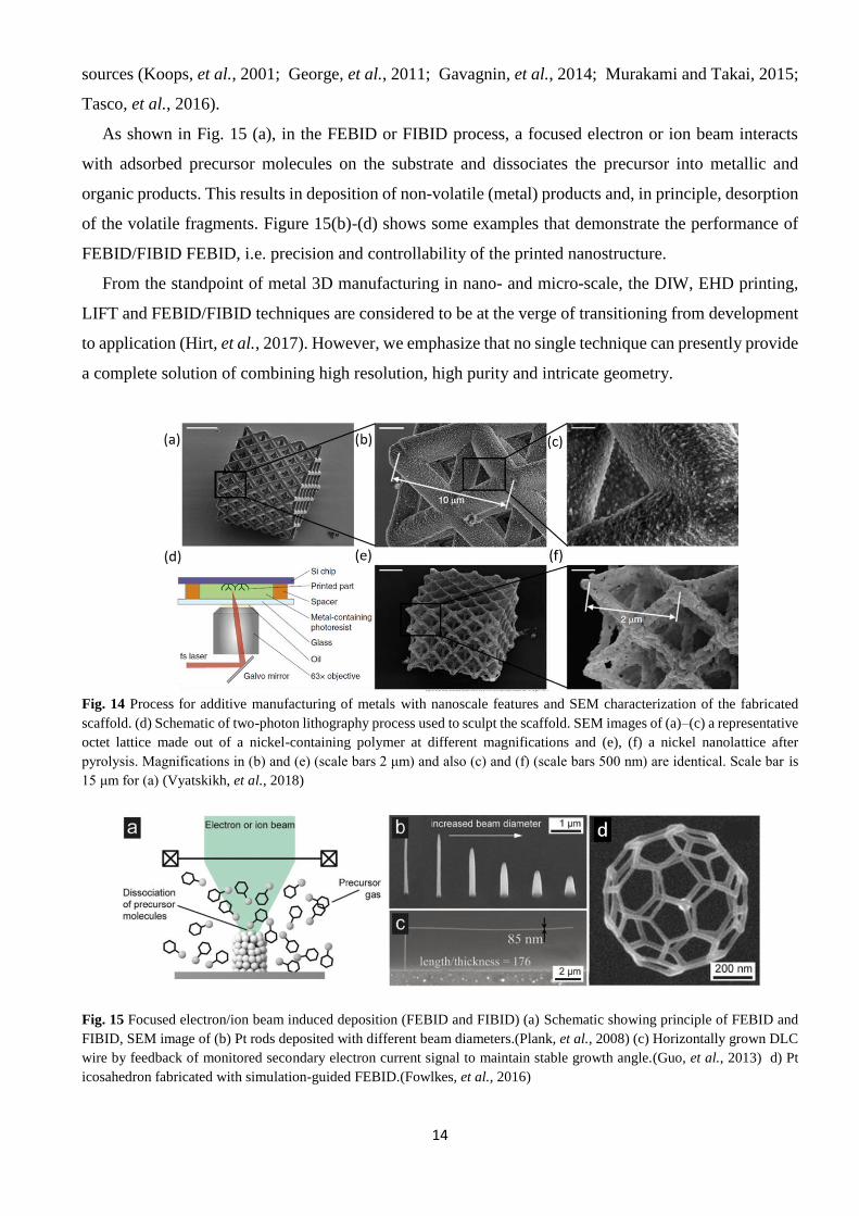
14
sources (Koops, et al., 2001; George, et al., 2011; Gavagnin, et al., 2014; Murakami and Takai, 2015;
Tasco, et al., 2016).
As shown in Fig. 15 (a), in the FEBID or FIBID process, a focused electron or ion beam interacts
with adsorbed precursor molecules on the substrate and dissociates the precursor into metallic and
organic products. This results in deposition of non-volatile (metal) products and, in principle, desorption
of the volatile fragments. Figure 15(b)-(d) shows some examples that demonstrate the performance of
FEBID/FIBID FEBID, i.e. precision and controllability of the printed nanostructure.
From the standpoint of metal 3D manufacturing in nano- and micro-scale, the DIW, EHD printing,
LIFT and FEBID/FIBID techniques are considered to be at the verge of transitioning from development
to application (Hirt, et al., 2017). However, we emphasize that no single technique can presently provide
a complete solution of combining high resolution, high purity and intricate geometry.
Fig. 14 Process for additive manufacturing of metals with nanoscale features and SEM characterization of the fabricated
scaffold. (d) Schematic of two-photon lithography process used to sculpt the scaffold. SEM images of (a)–(c) a representative
octet lattice made out of a nickel-containing polymer at different magnifications and (e), (f) a nickel nanolattice after
pyrolysis. Magnifications in (b) and (e) (scale bars 2 μm) and also (c) and (f) (scale bars 500 nm) are identical. Scale bar is
15 μm for (a) (Vyatskikh, et al., 2018)
Fig. 15 Focused electron/ion beam induced deposition (FEBID and FIBID) (a) Schematic showing principle of FEBID and
FIBID, SEM image of (b) Pt rods deposited with different beam diameters.(Plank, et al., 2008) (c) Horizontally grown DLC
wire by feedback of monitored secondary electron current signal to maintain stable growth angle.(Guo, et al., 2013) d) Pt
icosahedron fabricated with simulation-guided FEBID.(Fowlkes, et al., 2016)
15
2.2.3 Ceramic materials
In comparison to plastic and metal processing, the ceramic industry has been slow in implementing
additive manufacturing due to the difficulties with shape, a limited resolution and the quality of the
produced parts (Schwentenwein and Homa, 2015). However, as global trends point toward customized
design and manufacturing and increasing needs for complex nano- and microscale fabrication, it is
inevitable that additive manufacturing technologies are also promising for ceramic materials.
Selective laser sintering (SLS) and selective laser melting (SLM) are powder-based direct sintering
processes whereby the individual particles are connected using thermal energy by means of a laser.
However, significant internal stresses can be induced by high temperature gradients, which result in a
rough surface morphology.
On the other hand, indirect methods require a combined binder and ceramic particle mixture and a
post-treatment of printed ceramic parts. This is applicable to many polymer-based additive
manufacturing processes such as fused deposition modelling (FDM), stereolithography and digital light
processing (DLP).(Schwentenwein and Homa, 2015) Upon thermal treatment of the printed object, the
organic components are removed and the inorganic particles are sintered to form a high-purity ceramic
architecture. Schwentenwein et al.(Schwentenwein and Homa, 2015) demonstrated high density printed
alumina ceramic parts which have mechanical strength comparable to conventionally produced alumina
parts prepared using a photocurable ceramic suspension with light-emitting diodes (LEDs) combined
with a digital micromirror device. The process is known as lithography-based ceramic manufacturing
(LCM) because it is based on selective curing by a dynamic mask exposure process which enables
printed dense microscale features.
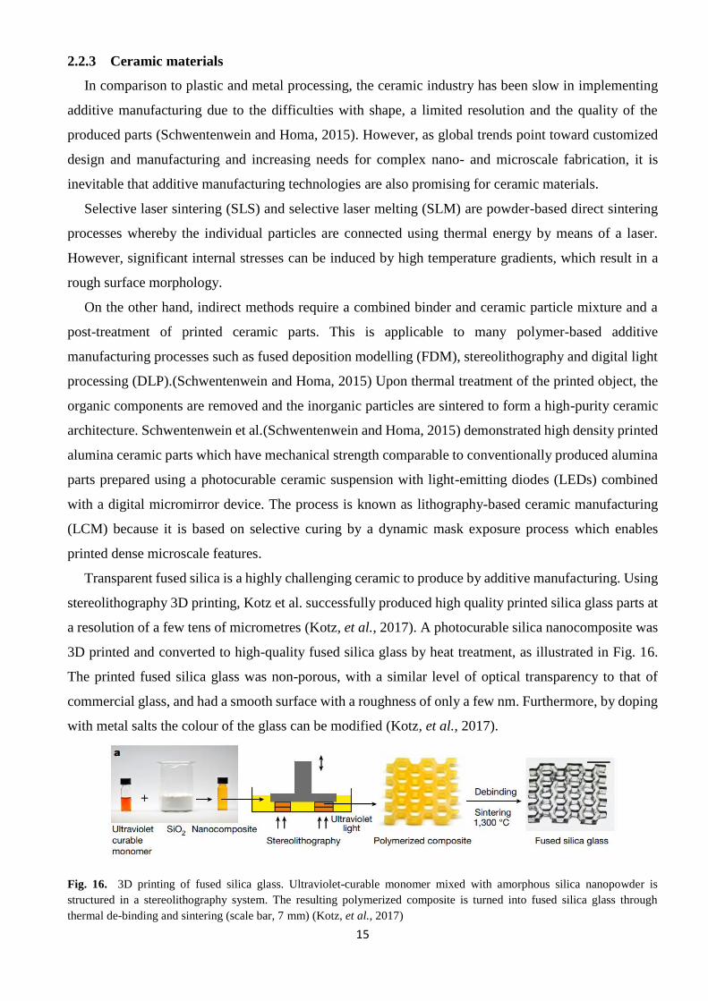
Transparent fused silica is a highly challenging ceramic to produce by additive manufacturing. Using
stereolithography 3D printing, Kotz et al. successfully produced high quality printed silica glass parts at
a resolution of a few tens of micrometres (Kotz, et al., 2017). A photocurable silica nanocomposite was
3D printed and converted to high-quality fused silica glass by heat treatment, as illustrated in Fig. 16.
The printed fused silica glass was non-porous, with a similar level of optical transparency to that of
commercial glass, and had a smooth surface with a roughness of only a few nm. Furthermore, by doping
with metal salts the colour of the glass can be modified (Kotz, et al., 2017).
Fig. 16. 3D printing of fused silica glass. Ultraviolet-curable monomer mixed with amorphous silica nanopowder is
structured in a stereolithography system. The resulting polymerized composite is turned into fused silica glass through
thermal de-binding and sintering (scale bar, 7 mm) (Kotz, et al., 2017)
16
2.3 Digital control and automation
In order to realize complex 3D structure in micro- or sub micro-scale, digital control and automation
are essential, forming a platform to build on using additive manufacturing. A wide range of CAD models
can be built, which are then transferred to STL (standard transform language) format to provide cross-
section data for each layer of 3D model by digital slicing of the CAD drawing. From there, the tool path
(i.e., printer nozzle or laser trajectory) is determined and the automated printing process can begin.
Examination and analysis of performance results for a wide range of compositional and structural
parameters is crucial to achieve design optimization and simulation. The complex icosahedron structure
of a previously shown Pt nanostructure built by FEBID (Fig. 15 (d)) was possible to fabricate using the
simulation-guided processing.(Fowlkes, et al., 2016) The simulation predicts beam-deposit interactions,
including spatial distribution of local precursor concentrations, and ‘guides’ the beam accordingly to
compensate for such effects. Furthermore, simulation-guided fabrication is considered beneficial for
solving other important challenges of additive manufacturing (DebRoy, et al., 2018). For example,
shrinkage and deformation of 3D printed structure after annealing are common issues for many metal
and ceramic materials. Simulation can help to predict the possible volume loss and geometrical
distortion. This result can be used to optimize the original design to compensate for the impact of thermal
treatment (DebRoy, et al., 2018).
Similarly to using optical monitoring for precise feedback control, the measured secondary electron
current can also be used for achieving a precisely controlled growth angle of the deposit in the FIBID
process (Bret, et al., 2004; Rack, et al., 2007). This real time monitoring and feedback control by
optical/electrical measurement can be instrumental for improving the stability of the process and the
quality of printed film or 3D architecture in the plasma printing system.
The use of simulations and precise control can therefore drastically improve the quality of the product
in terms of composition and structure, producing stable, complex 3D structures in a variety of materials.
2.4 Limitations for applications in micro- and nano-scale manufacturing
The surface textures of additively produced materials commonly require a surface finishing process
to improve the as-is printed surface characteristics. These include stair-like steps, powder adhesion, fill
patterns from extrusion or beam-based systems, and witness marks from support material removal can
be improved by choosing a fine filament in FDM; however, this significantly increases the build time.
Powder adhesion is a common issue in binding, powder bed and powder feed processes (Bahnini, et al.,
2018). To combat this, machining, shot peening and grinding have been widely used to achieve greater
surface quality. Chemical processes can also be used, such as electro-polishing. Generally, however,
these surface treatment methods are not applicable for microscale structuring. Objects sculpted by
additive manufacturing processes generally have inferior mechanical strength due to the intrinsic layer-
17
by-layer formation and lack of crosslinking between different layers as well as between the printed
structure and the substrate. Residual stresses and micropores often exist in the printed metallic parts,
which therefore require post thermal processing to improve their mechanical performance and provide
the desired microstructure. This is especially problematic when the structure is required to be built on
thermally weak materials or thin film-like substrates.
When sculpting composite materials or multi-material 3D objects the necessity of post-processing,
especially at high temperature, can limit the choice of materials and processing techniques. Intermittent
in situ annealing by laser has been proposed to enhance process efficiency and improve the distortion of
the sculpted object by removing the thermal post-processing step (Lewis, et al., 2015; Stanford, et al.,
2015). However, this intermittent annealing was time-consuming and caused a change in the operating
pressure due to the reactive gas supply, which interrupted the deposition process. Pre- and post-
treatments in additive manufacturing are considered inevitable to a certain extent, hence research has
mostly focussed on creating more facile post-processing methods instead of removing this step
completely.
The low reduction rate for certain metals deposition in FEBID/FIBID (Hirt, et al., 2017) is also an
area that requires further research. While Au, Co, Fe and Ge could be reduced almost completely, other
metals such as Ir, Mo and Ti show low reduction levels of under 35% (Botman, et al., 2009).
In contrast to FEBID/FIBID, which can only provide electrons or ions, plasma can provide a diverse
range of chemically reactive species. The dependence on the precursor materials is not as dominant when
using plasma and it may be possible to increase the metal reduction level even in composite material
printing. Many conventional additive manufacturing techniques require a separate process for each
different material printed in one object. Plasma CVD systems with precursor solution have the potential
to overcome this, achieving complex micro- or nano-fabrication in one step, either by mixing two (or
more) different liquid precursors or by installing two (or more) plasma jet systems next to each other.
In the following section, we shall discuss in more detail the mechanisms of plasma processing to
understand the benefits of plasmas and how plasma processes can potentially help overcome the
limitations and current issues of additive manufacturing.
3. Relevant plasma-specific effects
The obvious benefits of using low-temperature plasmas in printing technology are the diversity of
reactive species that exist and the multiple options for controlling them. Depending on electrode
configuration, operation pressure, electron energy and density, as well as the reactive gas environment,
the chemical and physical properties of the plasma can be manipulated using different controls. Surface
functionalization, etching, deposition and on-surface reactions are all examples of material modification
that can be carried out by controlling the plasma properties.
18
3.1 Surface functionalization
A successful example of the commercialization of atmospheric-pressure plasma processes is the
plasma surface modification of a wide range of polymeric substrates. Usually, the highly hydrophobic
properties of polymeric materials result in poor wetting and adhesion properties, which often cause
difficulties in various manufacturing processes; for example, chemical wet processing, printing,
deposition and bonding with a different film or layer. Plasma surface modifications can be used to
significantly increase hydrophilicity, even under high speed Roll-to-Roll (R2R) operating conditions.
Atmospheric-pressure plasmas generate high density electrons, ions and metastable species, including
reactive oxygen and nitrogen-containing reactive radicals even in inert gas discharge that impinge onto
the substrate due to its exposure to ambient air during the process. Atmospheric pressure plasma jets
have been used as an effective tool for introducing a chemical change on substrate materials with
hydrophilic functional groups such as =O , -OH, -O, or – NH, both in the presence and absence of an
additional oxygen source such as water vapor, air or pure oxygen gas.
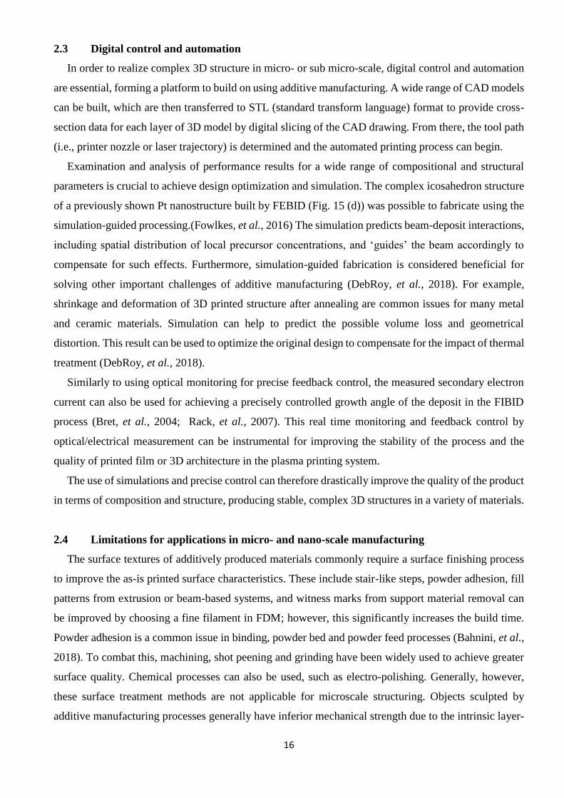
Figure 17 shows an example of surface modification used to increase hydrophilicity or
hydrophobicity, depending on the reactant gas condition. In Fig. 17, hydrophobicity is obtained by
depositing SiOx layers using an atomized organosilicon precursor such as TEOS (Tetraethyl
orthosilicate) or HMDSO (Hexamethyldisiloxane) (Verhoeven, et al., 2014). Changing the reactant gas
to a perfluorocarbon compound, for example CxFy or NF3, can even create a superhydrophobic surface
by replacing the C-H functional groups containing C-F bonds (Satulu, et al., 2016). This surface
modification function is important in printing applications as it enables selective modification using a
microplasma jet or pin-to-plate discharge configuration so that the surface energy and adhesion
properties can be modified locally, improving the resolution and durability of the printing process as
shown in Fig. 17 (g).
Fig. 17. Contact angle and surface wetting properties modified by the plasma treatment: Contact angle of water (a) before
plasma treatment (b) after plasma treatment by air (c) hydrophobic organosilicon film coated surface (d) – (f) corresponding
wetting properties of surface (a)-(c) respectively (g) selective modification in ~ 200 μm line width of polymeric surface by
atmospheric pressure plasma. (Verhoeven, et al., 2014) In panel (g), CA stands for contact angle.
19
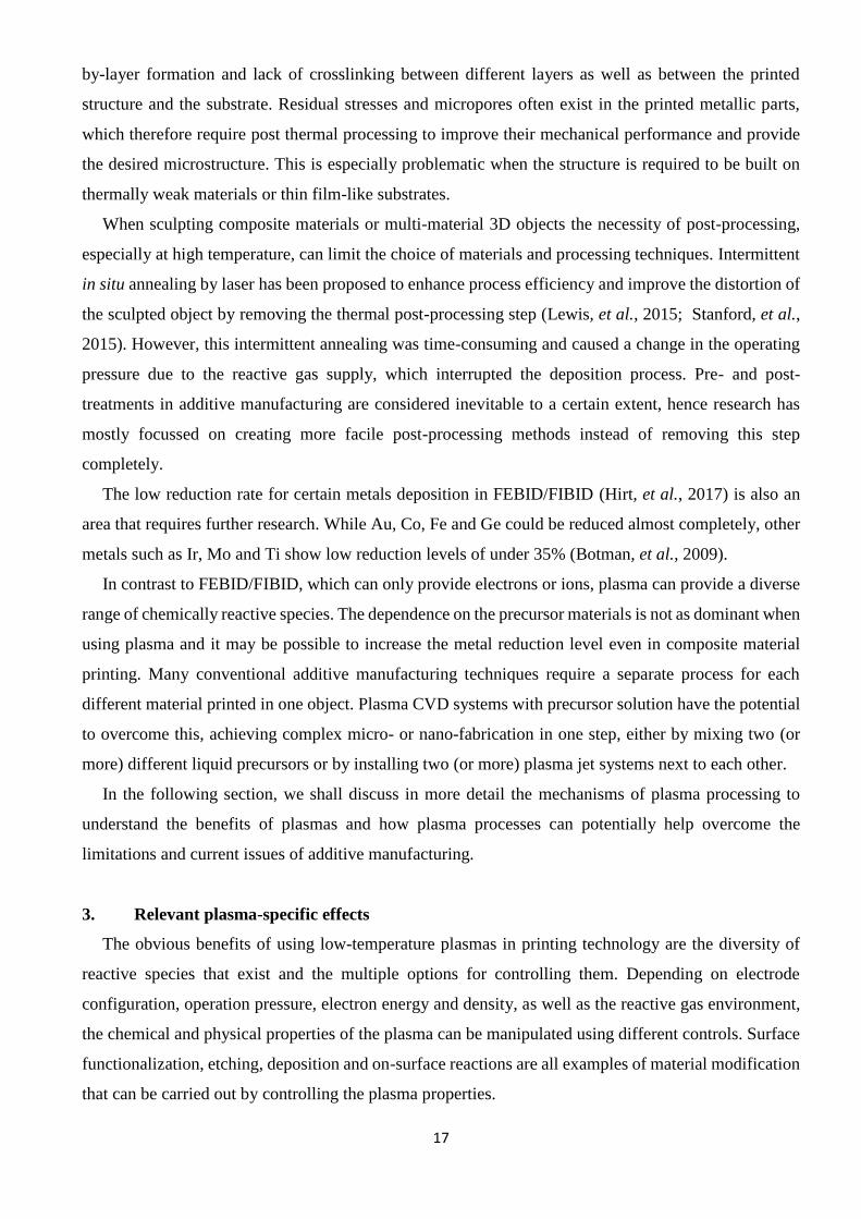
Yick et al. demonstrated the highly confined surface modification of vertically aligned carbon
nanotubes (VA-CNTs) for gold nanoparticle deposition using a microplasma jet, which can be beneficial
for selective patterning or printing with micrometre precision. This localized plasma treatment enabled
the production of a microfluidic strip that effectively confined Au nanoparticles to a 100 µm feature on
the VA-CNT support (Yick, et al., 2013). The deposited nanogold was found throughout the entire depth
(2.5 μm) of the microfluidic strip, which indicates a 3D Au–CNT hybrid formation over the entire
nanotube length. In additive manufacturing processes or decorative depositions on various substrates or
3D objects, this uniform and selective surface modification can be a versatile assisting tool and
processing technique.
Fig. 18. Plasma surface modifications to confine Au nanoparticles (Au NPs) within microscopic line features: (a) Schematic
of the surface modification and the nanogold deposition procedure. The microfluidic strips are highlighted in pink. (b) A
photo showing atmospheric pressure plasma jet and the plasma plume’s size. (c) Change in surface wettability of the VA-
CNTs in the plasma-modified (hydrophilic) and the pristine area (hydrophobic). Scale bars are 2 mm in (b) and (c). (d) Optical
micrograph at the interfacial region of Au and CNT (e) SEM image depicting the interfacial region (III). False color is applied
to highlight Au nanoparticles. SEM micrographs of the pristine (f) and the Au ND decorated (g) sides of the VA-CNTs,
corresponding to areas (I) and (IV) in (a), respectively. Insets in (c) and (d) are the corresponding high-resolution SEM
images (Yick, et al., 2013)
3.2 Etching
Plasma etching is one of the most common processes whereby plasma-generated chemical species
react with the surface atoms and remove them by forming volatile products. Due to the highly collisional
environment at atmospheric pressure, a significant physical sputtering effect by high energy ions, as in
low-pressure plasmas, cannot be expected. However, in many polymer materials such as polyethylene
(PE), polypropylene (PP), polycarbonate (PC) and poly(ether ether ketone) (PEEK) etc., it has been
shown by measurement of the mass loss and etch profiles after the plasma exposure that high etch rates
of 50 – 300 nm/s are possible (Fricke, et al., 2011). The experiments showed that reactive oxygen species
20
play an important role in the polymer etching process (Fricke, et al., 2011). The etching typically leads
to chemical changes on the surface and is very effective in changing the morphology of the substrate.
Indeed, depending on the process conditions, one can sculpt micro- or nano- structures of different
dimensionalities (1D-3D).
Plasma etching at atmospheric pressure is not limited to polymer materials. Thomson et al. showed
that etching by atmospheric-pressure DBD plasmas is an effective method for controlling the ZnO
surface morphology (Thomson, et al., 2013). Surface morphology is a critical parameter that determines
the optical scattering properties of transparent conducting oxides in photovoltaic thin films. The reactant
gases were found to have a significant effect on the etching process; in particular, water introduction has
been shown to be important for the efficient etching of ZnO. It was proposed that a two-stage reaction
process occurs, with intermediate products (e.g., a hydrate or partial hydrate) reacting faster with oxygen.
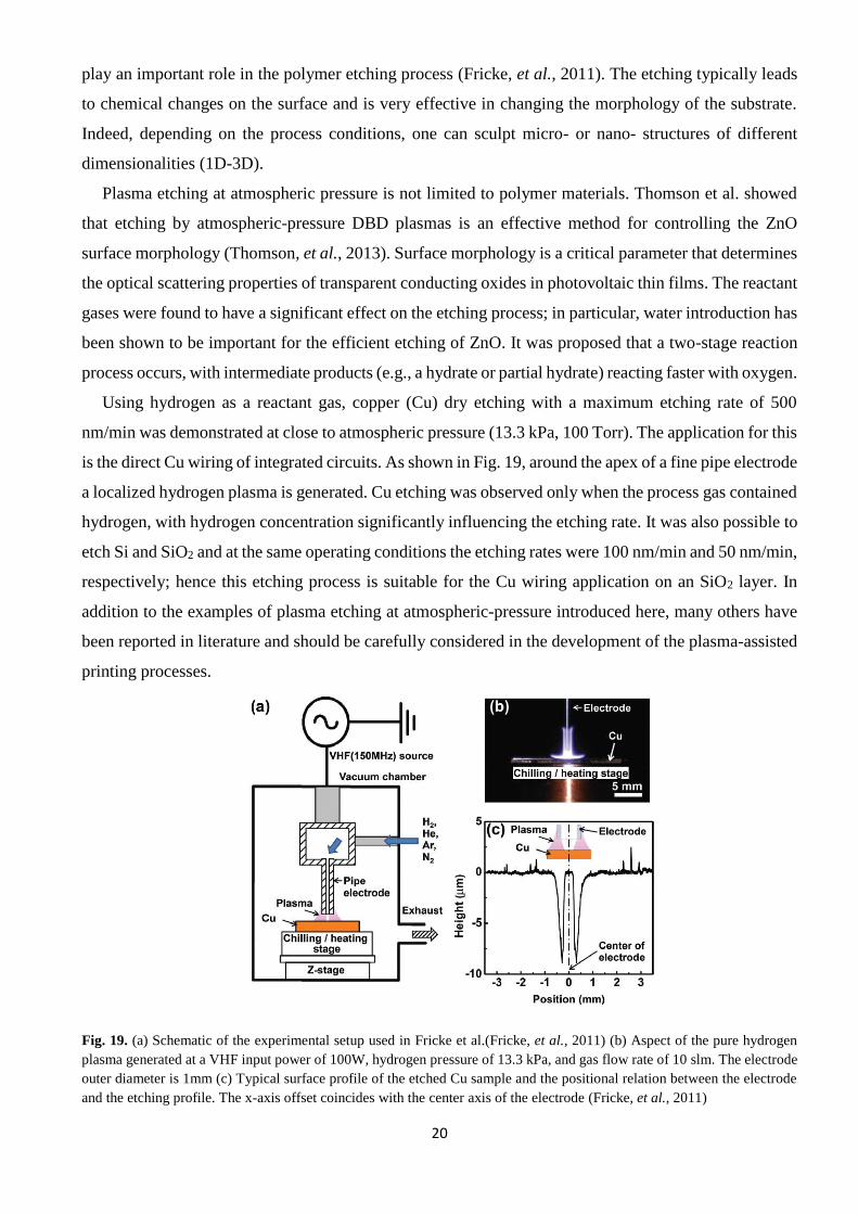
Using hydrogen as a reactant gas, copper (Cu) dry etching with a maximum etching rate of 500
nm/min was demonstrated at close to atmospheric pressure (13.3 kPa, 100 Torr). The application for this
is the direct Cu wiring of integrated circuits. As shown in Fig. 19, around the apex of a fine pipe electrode
a localized hydrogen plasma is generated. Cu etching was observed only when the process gas contained
hydrogen, with hydrogen concentration significantly influencing the etching rate. It was also possible to
etch Si and SiO2 and at the same operating conditions the etching rates were 100 nm/min and 50 nm/min,
respectively; hence this etching process is suitable for the Cu wiring application on an SiO2 layer. In
addition to the examples of plasma etching at atmospheric-pressure introduced here, many others have
been reported in literature and should be carefully considered in the development of the plasma-assisted
printing processes.
Fig. 19. (a) Schematic of the experimental setup used in Fricke et al.(Fricke, et al., 2011) (b) Aspect of the pure hydrogen
plasma generated at a VHF input power of 100W, hydrogen pressure of 13.3 kPa, and gas flow rate of 10 slm. The electrode
outer diameter is 1mm (c) Typical surface profile of the etched Cu sample and the positional relation between the electrode
and the etching profile. The x-axis offset coincides with the center axis of the electrode (Fricke, et al., 2011)
21
3.3 Deposition
Deposition is directly related to 2D and 3D printing processes as it builds up layers and architects
them in three dimensions. Plasma polymerization can be understood as an extension of deposition by
crosslinking monomers into larger molecules through the build-up of layers. The influence of different
species (ions, neutral species, and photons) on the polymerization process within the plasma discharge
was studied by examining the crosslinking properties. This was carried out by using a carefully designed
setup with different optical and metal windows to deconvolute the effects of the various plasma species
on the surface nanomechanical properties of polyethylene at low pressure (p ~ 500 mTorr). It was shown
that surface crosslinking is primarily due to the simultaneous effects of neutral species and vacuum
ultraviolet (VUV) photons, whilst the ion bombardment effect is secondary. The intensity of VUV may
differ at atmospheric-pressure conditions. However, predominantly high-density neutral radicals are
commonly available in atmospheric-pressure plasma discharges and are expected to have an important
role in polymer based additive manufacturing processes, improving the mechanical properties and
accelerating polymerization.
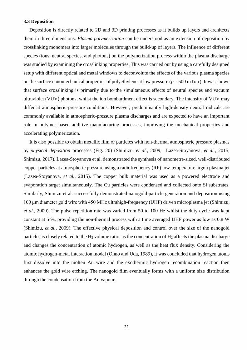
It is also possible to obtain metallic film or particles with non-thermal atmospheric pressure plasmas
by physical deposition processes (Fig. 20) (Shimizu, et al., 2009; Lazea-Stoyanova, et al., 2015;
Shimizu, 2017). Lazea-Stoyanova et al. demonstrated the synthesis of nanometre-sized, well-distributed
copper particles at atmospheric pressure using a radiofrequency (RF) low-temperature argon plasma jet
(Lazea-Stoyanova, et al., 2015). The copper bulk material was used as a powered electrode and
evaporation target simultaneously. The Cu particles were condensed and collected onto Si substrates.
Similarly, Shimizu et al. successfully demonstrated nanogold particle generation and deposition using
100 μm diameter gold wire with 450 MHz ultrahigh-frequency (UHF) driven microplasma jet (Shimizu,
et al., 2009). The pulse repetition rate was varied from 50 to 100 Hz whilst the duty cycle was kept
constant at 5 %, providing the non-thermal process with a time averaged UHF power as low as 0.8 W
(Shimizu, et al., 2009). The effective physical deposition and control over the size of the nanogold
particles is closely related to the H2 volume ratio, as the concentration of H2 affects the plasma discharge
and changes the concentration of atomic hydrogen, as well as the heat flux density. Considering the
atomic hydrogen-metal interaction model (Ohno and Uda, 1989), it was concluded that hydrogen atoms
first dissolve into the molten Au wire and the exothermic hydrogen recombination reaction then
enhances the gold wire etching. The nanogold film eventually forms with a uniform size distribution
through the condensation from the Au vapour.
22
Fig. 20. (a) Schematic of the microplasma setup used for nanogold synthesis (Shimizu, 2017) (b) Pulse-modulated
UHF voltage waveform effective for lowering gas temperature (c) Micro plasma jet touching finger without
thermal/electrical shock (Shimizu, et al., 2009) (d) SEM image showing finely controlled Au deposition (e)
Estimated size distribution (Shimizu, 2017)
In comparison to physical deposition, atmospheric pressure PECVD (AP-PECVD) shows more
flexibility in the range of materials that can be treated and the possibility of producing composite
materials with varying composition. SiOx deposition as a barrier coating for electronics, solar cells and
food packaging has been intensively investigated and successfully commercialized. Furthermore, metal
embedded SiOx films produced by high-temperature air plasmas are effective for antibacterial
applications. For example, hexamethyldisiloxane (HMDSO) was used as a primary precursor and
solutions with silver nitrate AgNO3, zinc nitrate Zn(NO3)2 and copper nitrate Cu(NO3)2, in a 1:1 volume
mixture of isopropanol and water, were sprayed into the plasma as secondary precursors (Zimmermann,
et al., 2011; Jager, et al., 2019). After separation from the precursor molecules, Ag, Zn and Cu elements
bind to oxygen, thus forming metal oxides that are subsequently incorporated into the SiOx film.
Amongst the range of target materials that can be produced using the AP-PECVD technique, it is
worthwhile to mention the growth of carbon nanotubes (CNT) from a C2H2 gas precursor (Kyung, et al.,
2006). The deposition was performed at 400oC using dielectric barrier discharge with He/C2H2, N2 and
NH3 addition. Interestingly, it was found that pre-treatment of the Ni catalyst can modify the surface
morphology, enhancing carbon diffusion during CNT formation. However, this process requires
substantial heating, which limits its applicability for plasma printing unless special arrangements are
made to print on sufficiently heated substrates.
In practice, chemical and physical deposition occur simultaneously in many cases, especially in
atmospheric pressure plasma processing. In the example of deposition of gold (Shimizu, et al., 2009),
the unique chemical environment of rich atomic hydrogen enabled the evaporation of solid gold without
any additional thermal energy source or sputtering aid. It is important to stress this benefit of the plasma
process, as the synergy between the chemical and physical effects may enable the fruition of several
processes of interest in additive manufacturing technology.
23
3.4 On-surface reactions
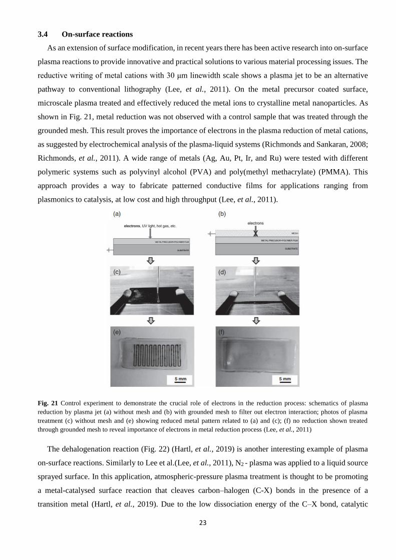
As an extension of surface modification, in recent years there has been active research into on-surface
plasma reactions to provide innovative and practical solutions to various material processing issues. The
reductive writing of metal cations with 30 μm linewidth scale shows a plasma jet to be an alternative
pathway to conventional lithography (Lee, et al., 2011). On the metal precursor coated surface,
microscale plasma treated and effectively reduced the metal ions to crystalline metal nanoparticles. As
shown in Fig. 21, metal reduction was not observed with a control sample that was treated through the
grounded mesh. This result proves the importance of electrons in the plasma reduction of metal cations,
as suggested by electrochemical analysis of the plasma-liquid systems (Richmonds and Sankaran, 2008;
Richmonds, et al., 2011). A wide range of metals (Ag, Au, Pt, Ir, and Ru) were tested with different
polymeric systems such as polyvinyl alcohol (PVA) and poly(methyl methacrylate) (PMMA). This
approach provides a way to fabricate patterned conductive films for applications ranging from
plasmonics to catalysis, at low cost and high throughput (Lee, et al., 2011).
Fig. 21 Control experiment to demonstrate the crucial role of electrons in the reduction process: schematics of plasma
reduction by plasma jet (a) without mesh and (b) with grounded mesh to filter out electron interaction; photos of plasma
treatment (c) without mesh and (e) showing reduced metal pattern related to (a) and (c); (f) no reduction shown treated
through grounded mesh to reveal importance of electrons in metal reduction process (Lee, et al., 2011)
The dehalogenation reaction (Fig. 22) (Hartl, et al., 2019) is another interesting example of plasma
on-surface reactions. Similarly to Lee et al.(Lee, et al., 2011), N2 - plasma was applied to a liquid source
sprayed surface. In this application, atmospheric-pressure plasma treatment is thought to be promoting
a metal-catalysed surface reaction that cleaves carbon–halogen (C-X) bonds in the presence of a
transition metal (Hartl, et al., 2019). Due to the low dissociation energy of the C–X bond, catalytic
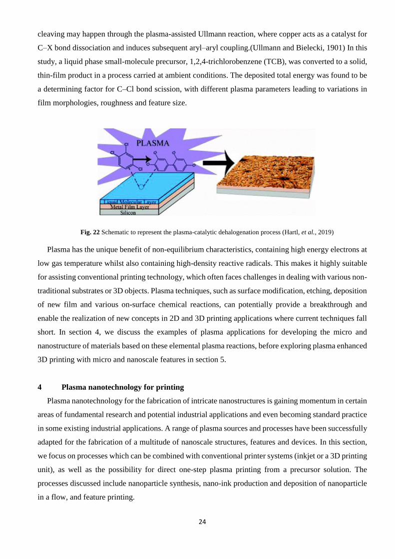
24
cleaving may happen through the plasma-assisted Ullmann reaction, where copper acts as a catalyst for
C–X bond dissociation and induces subsequent aryl–aryl coupling.(Ullmann and Bielecki, 1901) In this
study, a liquid phase small-molecule precursor, 1,2,4-trichlorobenzene (TCB), was converted to a solid,
thin-film product in a process carried at ambient conditions. The deposited total energy was found to be
a determining factor for C–Cl bond scission, with different plasma parameters leading to variations in
film morphologies, roughness and feature size.
Fig. 22 Schematic to represent the plasma-catalytic dehalogenation process (Hartl, et al., 2019)
Plasma has the unique benefit of non-equilibrium characteristics, containing high energy electrons at
low gas temperature whilst also containing high-density reactive radicals. This makes it highly suitable
for assisting conventional printing technology, which often faces challenges in dealing with various non-
traditional substrates or 3D objects. Plasma techniques, such as surface modification, etching, deposition
of new film and various on-surface chemical reactions, can potentially provide a breakthrough and
enable the realization of new concepts in 2D and 3D printing applications where current techniques fall
short. In section 4, we discuss the examples of plasma applications for developing the micro and
nanostructure of materials based on these elemental plasma reactions, before exploring plasma enhanced
3D printing with micro and nanoscale features in section 5.
4 Plasma nanotechnology for printing
Plasma nanotechnology for the fabrication of intricate nanostructures is gaining momentum in certain
areas of fundamental research and potential industrial applications and even becoming standard practice
in some existing industrial applications. A range of plasma sources and processes have been successfully
adapted for the fabrication of a multitude of nanoscale structures, features and devices. In this section,
we focus on processes which can be combined with conventional printer systems (inkjet or a 3D printing
unit), as well as the possibility for direct one-step plasma printing from a precursor solution. The
processes discussed include nanoparticle synthesis, nano-ink production and deposition of nanoparticle
in a flow, and feature printing.
25
4.1 Nanoparticle production
Metallurgical reduction, fuming, atomization, electrolysis, grinding, the sol-gel method, precipitation
and spray drying are typical conventional processes used for producing metallic powder (Young and
Pfender, 1985). Plasma-based fine metal powder synthesis methods are preferred because they provide
numerous particle types at high throughput and with good process control (Forster, et al., 2012; Lazea-
Stoyanova, et al., 2015).
4.1.1 Thermal plasma synthesis of nano-sized powders
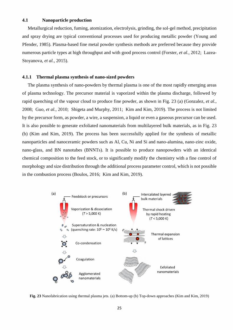
The plasma synthesis of nano-powders by thermal plasma is one of the most rapidly emerging areas
of plasma technology. The precursor material is vaporized within the plasma discharge, followed by
rapid quenching of the vapour cloud to produce fine powder, as shown in Fig. 23 (a) (Gonzalez, et al.,
2008; Guo, et al., 2010; Shigeta and Murphy, 2011; Kim and Kim, 2019). The process is not limited
by the precursor form, as powder, a wire, a suspension, a liquid or even a gaseous precursor can be used.
It is also possible to generate exfoliated nanomaterials from multilayered bulk materials, as in Fig. 23
(b) (Kim and Kim, 2019). The process has been successfully applied for the synthesis of metallic
nanoparticles and nanoceramic powders such as Al, Cu, Ni and Si and nano-alumina, nano-zinc oxide,
nano-glass, and BN nanotubes (BNNTs). It is possible to produce nanopowders with an identical
chemical composition to the feed stock, or to significantly modify the chemistry with a fine control of
morphology and size distribution through the additional process parameter control, which is not possible
in the combustion process (Boulos, 2016; Kim and Kim, 2019).
Fig. 23 Nanofabrication using thermal plasma jets. (a) Bottom-up (b) Top-down approaches (Kim and Kim, 2019)
26
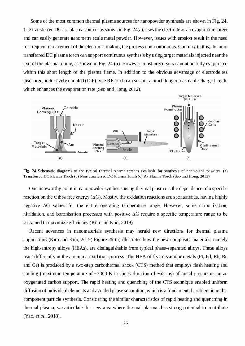
Some of the most common thermal plasma sources for nanopowder synthesis are shown in Fig. 24.
The transferred DC arc plasma source, as shown in Fig. 24(a), uses the electrode as an evaporation target
and can easily generate nanometre scale metal powder. However, issues with erosion result in the need
for frequent replacement of the electrode, making the process non-continuous. Contrary to this, the non-
transferred DC plasma torch can support continuous synthesis by using target materials injected near the
exit of the plasma plume, as shown in Fig. 24 (b). However, most precursors cannot be fully evaporated
within this short length of the plasma flame. In addition to the obvious advantage of electrodeless
discharge, inductively coupled (ICP) type RF torch can sustain a much longer plasma discharge length,
which enhances the evaporation rate (Seo and Hong, 2012).
Fig. 24 Schematic diagrams of the typical thermal plasma torches available for synthesis of nano-sized powders. (a)
Transferred DC Plasma Torch (b) Non-transferred DC Plasma Torch (c) RF Plasma Torch (Seo and Hong, 2012)
One noteworthy point in nanopowder synthesis using thermal plasma is the dependence of a specific
reaction on the Gibbs free energy (ΔG). Mostly, the oxidation reactions are spontaneous, having highly
negative ΔG values for the entire operating temperature range. However, some carbonization,
nitridation, and boronisation processes with positive ΔG require a specific temperature range to be
sustained to maximize efficiency (Kim and Kim, 2019).
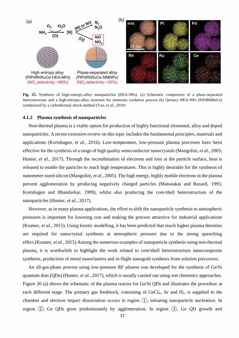
Recent advances in nanomaterials synthesis may herald new directions for thermal plasma
applications.(Kim and Kim, 2019) Figure 25 (a) illustrates how the new composite materials, namely
the high-entropy alloys (HEAs), are distinguishable from typical phase-separated alloys. These alloys
react differently in the ammonia oxidation process. The HEA of five dissimilar metals (Pt, Pd, Rh, Ru
and Ce) is produced by a two-step carbothermal shock (CTS) method that employs flash heating and
cooling (maximum temperature of ~2000 K in shock duration of ~55 ms) of metal precursors on an
oxygenated carbon support. The rapid heating and quenching of the CTS technique enabled uniform
diffusion of individual elements and avoided phase separation, which is a fundamental problem in multi-
component particle synthesis. Considering the similar characteristics of rapid heating and quenching in
thermal plasma, we articulate this new area where thermal plasmas has strong potential to contribute
(Yao, et al., 2018).
27
Fig. 25. Synthesis of high-entropy-alloy nanoparticles (HEA-NPs). (a) Schematic comparison of a phase-separated
heterostructure and a high-entropy-alloy structure for ammonia oxidation process (b) Quinary HEA-NPs (PtPdRhRuCe)
synthesized by a carbothermal shock method (Yao, et al., 2018)
4.1.2 Plasma synthesis of nanoparticles
Non-thermal plasma is a viable option for production of highly functional elemental, alloy and doped
nanoparticles. A recent extensive review on this topic includes the fundamental principles, materials and
applications (Kortshagen, et al., 2016). Low-temperature, low-pressure plasma processes have been
effective for the synthesis of a range of high quality semiconductor nanocrystals (Mangolini, et al., 2005;
Hunter, et al., 2017). Through the recombination of electrons and ions at the particle surface, heat is
released to enable the particles to reach high temperatures. This is highly desirable for the synthesis of
nanometer-sized silicon (Mangolini, et al., 2005). The high energy, highly mobile electrons in the plasma
prevent agglomeration by producing negatively charged particles (Matsoukas and Russell, 1995;
Kortshagen and Bhandarkar, 1999), whilst also producing the core/shell heterostructure of the
nanoparticles (Hunter, et al., 2017).
However, as in many plasma applications, the effort to shift the nanoparticle synthesis to atmospheric
pressures is important for lowering cost and making the process attractive for industrial applications
(Kramer, et al., 2015). Using kinetic modelling, it has been predicted that much higher plasma densities
are required for nanocrystal synthesis at atmospheric pressure due to the strong quenching
effect.(Kramer, et al., 2015) Among the numerous examples of nanoparticle synthesis using non-thermal
plasma, it is worthwhile to highlight the work related to core/shell heterostructure nanocomposite
synthesis, production of metal nanoclusters and in-flight nanogold synthesis from solution precursors.
An all-gas-phase process using low-pressure RF plasma was developed for the synthesis of Ge/Si
quantum dots (QDs) (Hunter, et al., 2017), which is usually carried out using wet chemistry approaches.
Figure 26 (a) shows the schematic of the plasma reactor for Ge/Si QDs and illustrates the procedure at
each different stage. The primary gas feedstock, consisting of GeCl4, Ar and H2, is supplied to the
chamber and electron impact dissociation occurs in region ①, initiating nanoparticle nucleation. In
region ②, Ge QDs grow predominantly by agglomeration. In region ③, Ge QD growth and
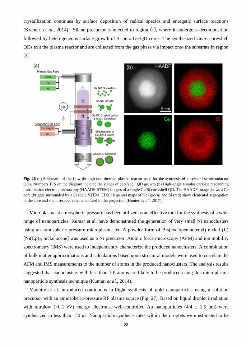
28
crystallization continues by surface deposition of radical species and energetic surface reactions
(Kramer, et al., 2014). Silane precursor is injected to region ④, where it undergoes decomposition
followed by heterogeneous surface growth of Si onto Ge QD cores. The synthesized Ge/Si core/shell
QDs exit the plasma reactor and are collected from the gas phase via impact onto the substrate in region
⑤.
Fig. 26 (a) Schematic of the flow-through non-thermal plasma reactor used for the synthesis of core/shell semiconductor
QDs. Numbers 1−5 on the diagram indicate the stages of core/shell QD growth (b) High-angle annular dark-field scanning
transmission electron microscopy (HAADF-STEM) images of a single Ge/Si core/shell QD. The HAADF image shows a Ge
core (bright) surrounded by a Si shell. STEM−EDX elemental maps of Ge (green) and Si (red) show elemental segregation
to the core and shell, respectively, as viewed in the projection (Hunter, et al., 2017).
Microplasma at atmospheric pressure has been utilized as an effective tool for the synthesis of a wide
range of nanoparticles. Kumar et al. have demonstrated the generation of very small Ni nanoclusters
using an atmospheric pressure microplasma jet. A powder form of Bis(cyclopentadienyl) nickel (II)
[Ni(Cp)2, nickelocene] was used as a Ni precursor. Atomic force microscopy (AFM) and ion mobility
spectrometry (IMS) were used to independently characterize the produced nanoclusters. A combination
of bulk matter approximations and calculations based upon structural models were used to correlate the
AFM and IMS measurements to the number of atoms in the produced nanoclusters. The analysis results
suggested that nanoclusters with less than 102 atoms are likely to be produced using this microplasma
nanoparticle synthesis technique (Kumar, et al., 2014).
Maquire et al. introduced continuous in-flight synthesis of gold nanoparticles using a solution
precursor with an atmospheric-pressure RF plasma source (Fig. 27). Based on liquid droplet irradiation
with ultralow (<0.1 eV) energy electrons, well-controlled Au nanoparticles (4.4 ± 1.5 nm) were
synthesized in less than 150 μs. Nanoparticle synthesis rates within the droplets were estimated to be
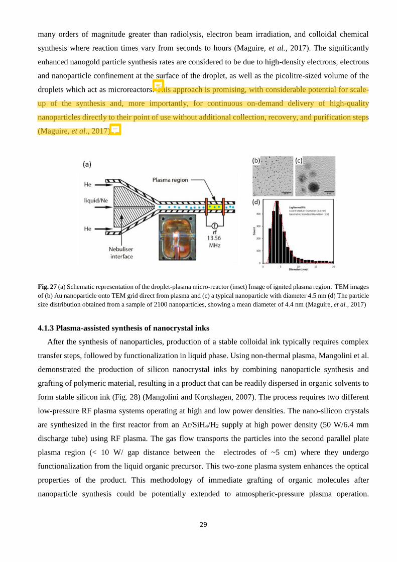
29
many orders of magnitude greater than radiolysis, electron beam irradiation, and colloidal chemical
synthesis where reaction times vary from seconds to hours (Maguire, et al., 2017). The significantly
enhanced nanogold particle synthesis rates are considered to be due to high-density electrons, electrons
and nanoparticle confinement at the surface of the droplet, as well as the picolitre-sized volume of the
droplets which act as microreactors. This approach is promising, with considerable potential for scale-
up of the synthesis and, more importantly, for continuous on-demand delivery of high-quality
nanoparticles directly to their point of use without additional collection, recovery, and purification steps
(Maguire, et al., 2017).
Fig. 27 (a) Schematic representation of the droplet-plasma micro-reactor (inset) Image of ignited plasma region. TEM images
of (b) Au nanoparticle onto TEM grid direct from plasma and (c) a typical nanoparticle with diameter 4.5 nm (d) The particle
size distribution obtained from a sample of 2100 nanoparticles, showing a mean diameter of 4.4 nm (Maguire, et al., 2017)
4.1.3 Plasma-assisted synthesis of nanocrystal inks
After the synthesis of nanoparticles, production of a stable colloidal ink typically requires complex
transfer steps, followed by functionalization in liquid phase. Using non-thermal plasma, Mangolini et al.
demonstrated the production of silicon nanocrystal inks by combining nanoparticle synthesis and
grafting of polymeric material, resulting in a product that can be readily dispersed in organic solvents to
form stable silicon ink (Fig. 28) (Mangolini and Kortshagen, 2007). The process requires two different
low-pressure RF plasma systems operating at high and low power densities. The nano-silicon crystals
are synthesized in the first reactor from an Ar/SiH4/H2 supply at high power density (50 W/6.4 mm
discharge tube) using RF plasma. The gas flow transports the particles into the second parallel plate
plasma region (< 10 W/ gap distance between the electrodes of ~5 cm) where they undergo
functionalization from the liquid organic precursor. This two-zone plasma system enhances the optical
properties of the product. This methodology of immediate grafting of organic molecules after
nanoparticle synthesis could be potentially extended to atmospheric-pressure plasma operation.
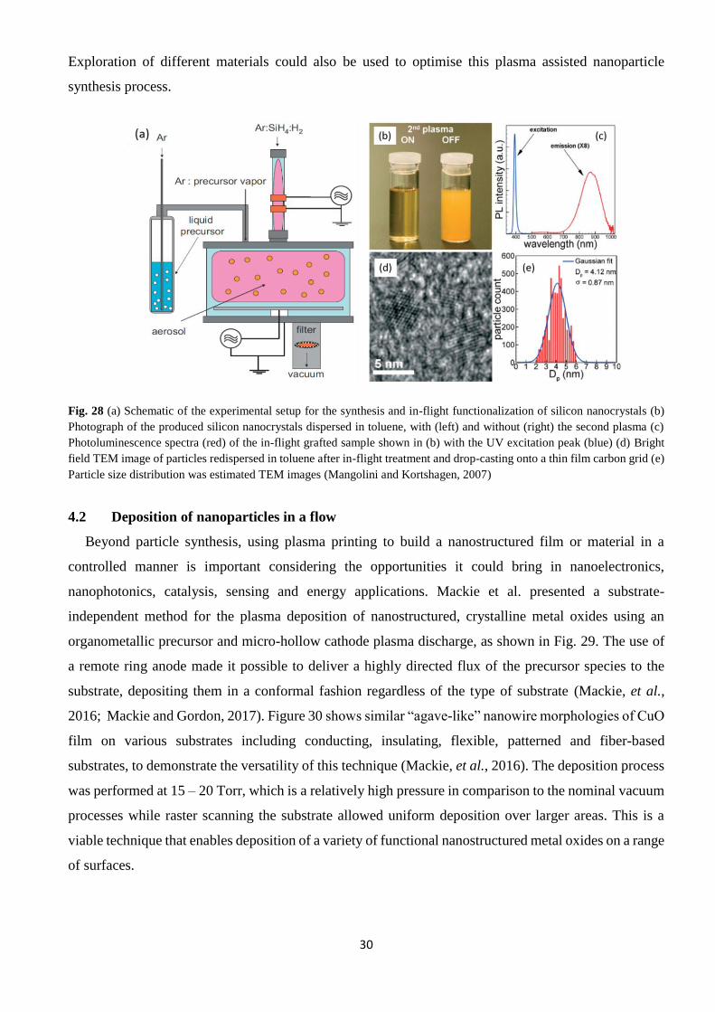
30
Exploration of different materials could also be used to optimise this plasma assisted nanoparticle
synthesis process.
Fig. 28 (a) Schematic of the experimental setup for the synthesis and in-flight functionalization of silicon nanocrystals (b)
Photograph of the produced silicon nanocrystals dispersed in toluene, with (left) and without (right) the second plasma (c)
Photoluminescence spectra (red) of the in-flight grafted sample shown in (b) with the UV excitation peak (blue) (d) Bright
field TEM image of particles redispersed in toluene after in-flight treatment and drop-casting onto a thin film carbon grid (e)
Particle size distribution was estimated TEM images (Mangolini and Kortshagen, 2007)
4.2 Deposition of nanoparticles in a flow
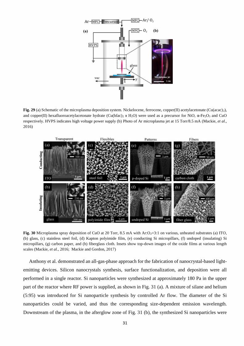
Beyond particle synthesis, using plasma printing to build a nanostructured film or material in a
controlled manner is important considering the opportunities it could bring in nanoelectronics,
nanophotonics, catalysis, sensing and energy applications. Mackie et al. presented a substrate-
independent method for the plasma deposition of nanostructured, crystalline metal oxides using an
organometallic precursor and micro-hollow cathode plasma discharge, as shown in Fig. 29. The use of
a remote ring anode made it possible to deliver a highly directed flux of the precursor species to the
substrate, depositing them in a conformal fashion regardless of the type of substrate (Mackie, et al.,
2016; Mackie and Gordon, 2017). Figure 30 shows similar “agave-like” nanowire morphologies of CuO
film on various substrates including conducting, insulating, flexible, patterned and fiber-based
substrates, to demonstrate the versatility of this technique (Mackie, et al., 2016). The deposition process
was performed at 15 – 20 Torr, which is a relatively high pressure in comparison to the nominal vacuum
processes while raster scanning the substrate allowed uniform deposition over larger areas. This is a
viable technique that enables deposition of a variety of functional nanostructured metal oxides on a range
of surfaces.
31
Fig. 29 (a) Schematic of the microplasma deposition system. Nickelocene, ferrocene, copper(II) acetylacetonate (Cu(acac)2),
and copper(II) hexafluoroacetylacetonate hydrate (Cu(hfac)2 x H2O) were used as a precursor for NiO, α-Fe2O3 and CuO
respectively. HVPS indicates high voltage power supply (b) Photo of Ar microplasma jet at 15 Torr/8.5 mA (Mackie, et al.,
2016)
Fig. 30 Microplasma spray deposition of CuO at 20 Torr, 8.5 mA with Ar:O2=3:1 on various, unheated substrates (a) ITO,
(b) glass, (c) stainless steel foil, (d) Kapton polyimide film, (e) conducting Si micropillars, (f) undoped (insulating) Si
micropillars, (g) carbon paper, and (h) fiberglass cloth. Insets show top-down images of the oxide films at various length
scales (Mackie, et al., 2016; Mackie and Gordon, 2017)
Anthony et al. demonstrated an all-gas-phase approach for the fabrication of nanocrystal-based light-
emitting devices. Silicon nanocrystals synthesis, surface functionalization, and deposition were all
performed in a single reactor. Si nanoparticles were synthesized at approximately 180 Pa in the upper
part of the reactor where RF power is supplied, as shown in Fig. 31 (a). A mixture of silane and helium
(5:95) was introduced for Si nanoparticle synthesis by controlled Ar flow. The diameter of the Si
nanoparticles could be varied, and thus the corresponding size-dependent emission wavelength.
Downstream of the plasma, in the afterglow zone of Fig. 31 (b), the synthesized Si nanoparticles were
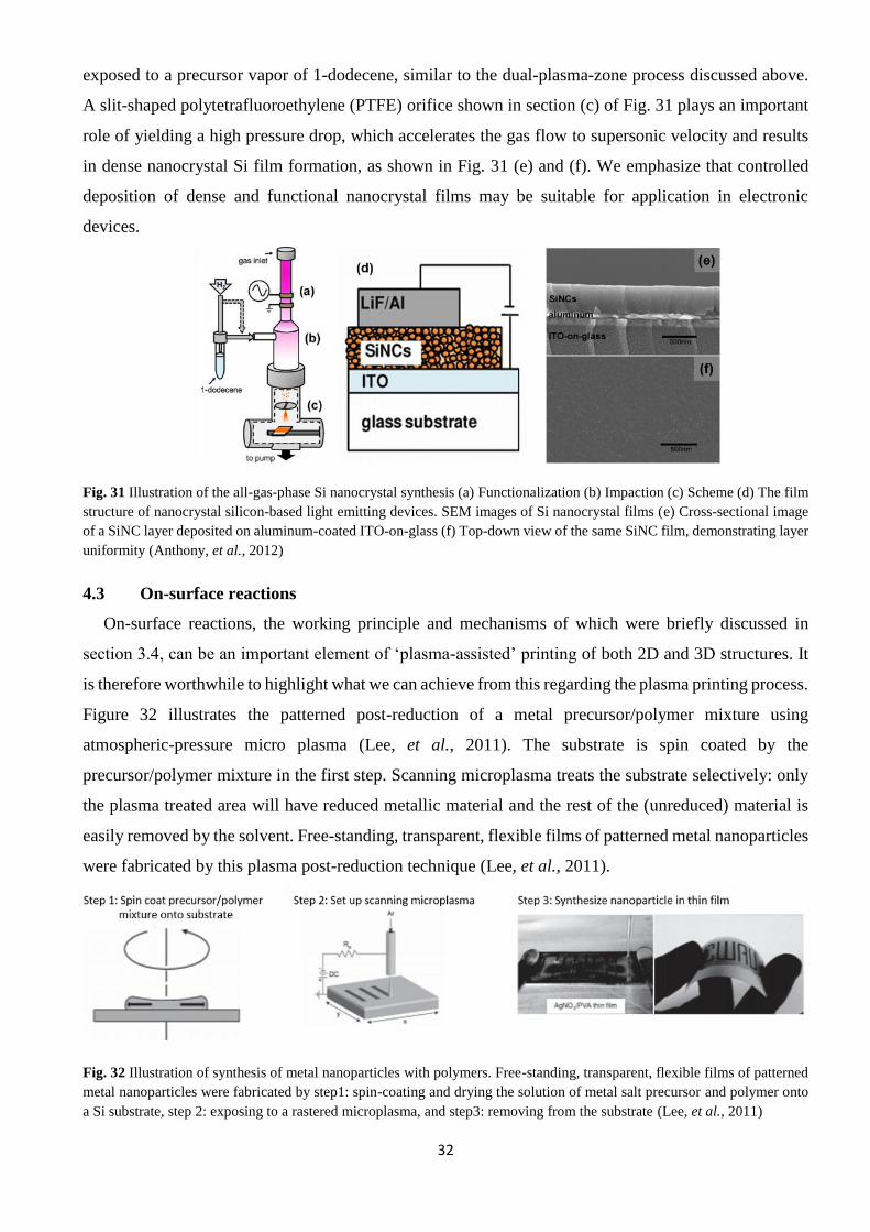
32
exposed to a precursor vapor of 1-dodecene, similar to the dual-plasma-zone process discussed above.
A slit-shaped polytetrafluoroethylene (PTFE) orifice shown in section (c) of Fig. 31 plays an important
role of yielding a high pressure drop, which accelerates the gas flow to supersonic velocity and results
in dense nanocrystal Si film formation, as shown in Fig. 31 (e) and (f). We emphasize that controlled
deposition of dense and functional nanocrystal films may be suitable for application in electronic
devices.
Fig. 31 Illustration of the all-gas-phase Si nanocrystal synthesis (a) Functionalization (b) Impaction (c) Scheme (d) The film
structure of nanocrystal silicon-based light emitting devices. SEM images of Si nanocrystal films (e) Cross-sectional image
of a SiNC layer deposited on aluminum-coated ITO-on-glass (f) Top-down view of the same SiNC film, demonstrating layer
uniformity (Anthony, et al., 2012)
4.3 On-surface reactions
On-surface reactions, the working principle and mechanisms of which were briefly discussed in
section 3.4, can be an important element of ‘plasma-assisted’ printing of both 2D and 3D structures. It
is therefore worthwhile to highlight what we can achieve from this regarding the plasma printing process.
Figure 32 illustrates the patterned post-reduction of a metal precursor/polymer mixture using
atmospheric-pressure micro plasma (Lee, et al., 2011). The substrate is spin coated by the
precursor/polymer mixture in the first step. Scanning microplasma treats the substrate selectively: only
the plasma treated area will have reduced metallic material and the rest of the (unreduced) material is
easily removed by the solvent. Free-standing, transparent, flexible films of patterned metal nanoparticles
were fabricated by this plasma post-reduction technique (Lee, et al., 2011).
Fig. 32 Illustration of synthesis of metal nanoparticles with polymers. Free-standing, transparent, flexible films of patterned
metal nanoparticles were fabricated by step1: spin-coating and drying the solution of metal salt precursor and polymer onto
a Si substrate, step 2: exposing to a rastered microplasma, and step3: removing from the substrate (Lee, et al., 2011)
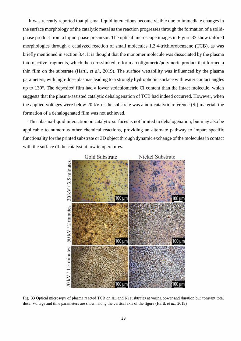
33
It was recently reported that plasma–liquid interactions become visible due to immediate changes in
the surface morphology of the catalytic metal as the reaction progresses through the formation of a solid-
phase product from a liquid-phase precursor. The optical microscope images in Figure 33 show tailored
morphologies through a catalyzed reaction of small molecules 1,2,4-trichlorobenzene (TCB), as was
briefly mentioned in section 3.4. It is thought that the monomer molecule was dissociated by the plasma
into reactive fragments, which then crosslinked to form an oligomeric/polymeric product that formed a
thin film on the substrate (Hartl, et al., 2019). The surface wettability was influenced by the plasma
parameters, with high-dose plasmas leading to a strongly hydrophobic surface with water contact angles
up to 130°. The deposited film had a lower stoichiometric Cl content than the intact molecule, which
suggests that the plasma-assisted catalytic dehalogenation of TCB had indeed occurred. However, when
the applied voltages were below 20 kV or the substrate was a non-catalytic reference (Si) material, the
formation of a dehalogenated film was not achieved.
This plasma-liquid interaction on catalytic surfaces is not limited to dehalogenation, but may also be
applicable to numerous other chemical reactions, providing an alternate pathway to impart specific
functionality for the printed substrate or 3D object through dynamic exchange of the molecules in contact
with the surface of the catalyst at low temperatures.
Fig. 33 Optical microsopy of plasma reacted TCB on Au and Ni susbtrates at varing power and duration but constant total
dose. Voltage and time parameters are shown along the vertical axis of the figure (Hartl, et al., 2019)
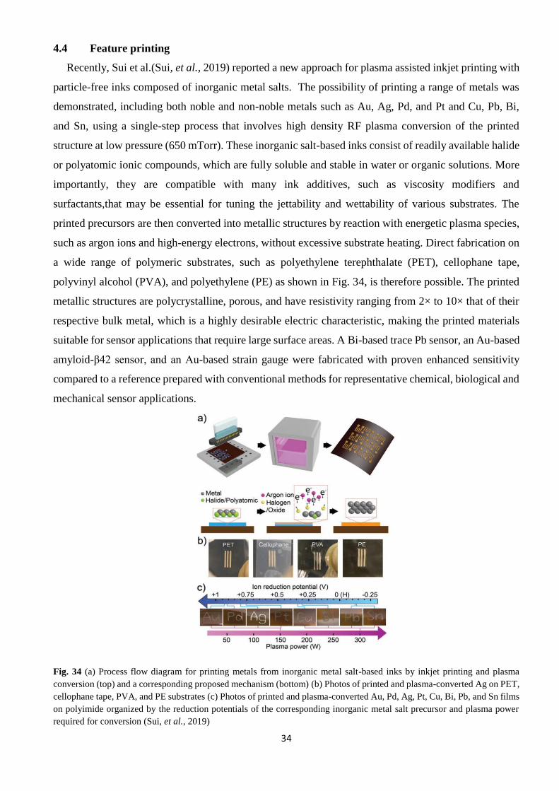
34
4.4 Feature printing
Recently, Sui et al.(Sui, et al., 2019) reported a new approach for plasma assisted inkjet printing with
particle-free inks composed of inorganic metal salts. The possibility of printing a range of metals was
demonstrated, including both noble and non-noble metals such as Au, Ag, Pd, and Pt and Cu, Pb, Bi,
and Sn, using a single-step process that involves high density RF plasma conversion of the printed
structure at low pressure (650 mTorr). These inorganic salt-based inks consist of readily available halide
or polyatomic ionic compounds, which are fully soluble and stable in water or organic solutions. More
importantly, they are compatible with many ink additives, such as viscosity modifiers and
surfactants,that may be essential for tuning the jettability and wettability of various substrates. The
printed precursors are then converted into metallic structures by reaction with energetic plasma species,
such as argon ions and high-energy electrons, without excessive substrate heating. Direct fabrication on
a wide range of polymeric substrates, such as polyethylene terephthalate (PET), cellophane tape,
polyvinyl alcohol (PVA), and polyethylene (PE) as shown in Fig. 34, is therefore possible. The printed
metallic structures are polycrystalline, porous, and have resistivity ranging from 2× to 10× that of their
respective bulk metal, which is a highly desirable electric characteristic, making the printed materials
suitable for sensor applications that require large surface areas. A Bi-based trace Pb sensor, an Au-based
amyloid-β42 sensor, and an Au-based strain gauge were fabricated with proven enhanced sensitivity
compared to a reference prepared with conventional methods for representative chemical, biological and
mechanical sensor applications.
Fig. 34 (a) Process flow diagram for printing metals from inorganic metal salt-based inks by inkjet printing and plasma
conversion (top) and a corresponding proposed mechanism (bottom) (b) Photos of printed and plasma-converted Ag on PET,
cellophane tape, PVA, and PE substrates (c) Photos of printed and plasma-converted Au, Pd, Ag, Pt, Cu, Bi, Pb, and Sn films
on polyimide organized by the reduction potentials of the corresponding inorganic metal salt precursor and plasma power
required for conversion (Sui, et al., 2019)
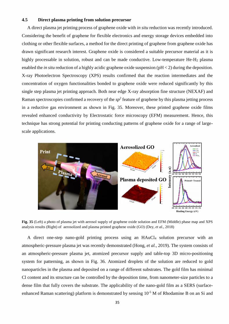
35
4.5 Direct plasma printing from solution precursor
A direct plasma jet printing process of graphene oxide with in situ reduction was recently introduced.
Considering the benefit of graphene for flexible electronics and energy storage devices embedded into
clothing or other flexible surfaces, a method for the direct printing of graphene from graphene oxide has
drawn significant research interest. Graphene oxide is considered a suitable precursor material as it is
highly processable in solution, robust and can be made conductive. Low-temperature He-H2 plasma
enabled the in situ reduction of a highly acidic graphene oxide suspension (pH < 2) during the deposition.
X-ray Photoelectron Spectroscopy (XPS) results confirmed that the reaction intermediates and the
concentration of oxygen functionalities bonded to graphene oxide were reduced significantly by this
single step plasma jet printing approach. Both near edge X-ray absorption fine structure (NEXAF) and
Raman spectroscopies confirmed a recovery of the sp2 feature of graphene by this plasma jetting process
in a reductive gas environment as shown in Fig. 35. Moreover, these printed graphene oxide films
revealed enhanced conductivity by Electrostatic force microscopy (EFM) measurement. Hence, this
technique has strong potential for printing conducting patterns of graphene oxide for a range of large-
scale applications.
Fig. 35 (Left) a photo of plasma jet with aerosol supply of graphene oxide solution and EFM (Middle) phase map and XPS
analysis results (Right) of aerosolized and plasma printed graphene oxide (GO) (Dey, et al., 2018)
A direct one-step nano-gold printing process using an HAuCl4 solution precursor with an
atmospheric-pressure plasma jet was recently demonstrated (Hong, et al., 2019). The system consists of
an atmospheric-pressure plasma jet, atomized precursor supply and table-top 3D micro-positioning
system for patterning, as shown in Fig. 36. Atomized droplets of the solution are reduced to gold
nanoparticles in the plasma and deposited on a range of different substrates. The gold film has minimal
Cl content and its structure can be controlled by the deposition time, from nanometer-size particles to a
dense film that fully covers the substrate. The applicability of the nano-gold film as a SERS (surface-
enhanced Raman scattering) platform is demonstrated by sensing 10-5 M of Rhodamine B on an Si and
36
paper substrate. This gold production process is readily applicable to various solution-based metal
precursors, providing an easily approachable method for composite material synthesis and printing.
Fig. 36 (a) Schematic of the plasma printing system with atmospheric-pressure plasma jet (b) Photo of discharge showing
liquid and gas input with nebulizer (c) Illustration of plasma reduction process in different parts of the system of Fig. 1(a),
where AuxCly indicates possible unreduced ionic gold in the discharge and on the surface e.g. AuIIICl4- or AuICl2
- (Hong, et
al., 2019)
The representative plasma sources and processes discussed above are suitable for a ranges of
application and can be utilized to improve the current printing technologies. In the following section 5,
we will review research related to 3D structure morphing using plasma processing.
5. Plasma combined with 3D printing
Combining 3D printing with plasmas is promising to advance current printing technologies. This non-
equilibrium media provides numerous effects of the plasma-excited species, which may lead to new
processes with enhanced capabilities at low process temperatures.
5.1. Plasma-aided localized CVD
The use of plasma in additive manufacturing began with the simple localized technique of plasma-
enhanced chemical vapour deposition (PECVD), with pioneering works by Holländer et al.(Hollander
and Abhinandan, 2003; Abhinandan and Hollander, 2004; Silmy, et al., 2005) and Shimizu et
al.(Shimizu, et al., 2003), but has since expanded. The traditional role of plasmas in CVD was to lower
the deposition temperature, thus increasing the range of substrates that could be employed. In this
process, the localization of the deposition can be ensured through the use of capillaries; by pulling a
glass tube under controlled conditions (i.e. under dry nitrogen, as glass is sensitive to water, and with an
accurate control of the temperature – usually satisfied by laser heating), it is relatively easy to reach
reproducible aperture sizes around several hundreds of nanometres, leading to unprecedented resolution
(Boileau, et al., 2016).
The main advantages of these processes are:
37
Possible control of the size of the basic pattern;
The possibility to deposit any material if liquid (with a sufficiently high partial pressure) or
gaseous precursors are available; and
The simple assembly of multiple materials.
This has been successfully carried out by localized plasma modification and combined atomic layer
deposition (ALD) process using μPlasmaPrinting system developed by Innophysics (Verkuijlen, et al.,
2014; Mameli, et al., 2017). However, this process also has certain drawbacks, the most common of
which are:
A relatively low writing speed (the highest possible deposition rate by CVD is around hundreds
of micrometres per second (Hollander and Abhinandan, 2003), leading to very porous structures);
The need for precise control of the surrounding atmosphere, which is required to limit the
presence of impurities (air and water to be removed for exact control of the deposit composition);
and
A limited efficiency for treatment of large areas
At a given resolution, the writing speed is comparable to those of laser treatments or ink-jet printers
but much lower than Digital Light Processing, where a digital light projector is used to flash a single
image of each layer. The use of the many capillaries in parallel improves the global writing efficiency,
but at the expense of a complicated control of gas injection.
To compete with conventional 3D printing solutions, plasma sources must operate at atmospheric
pressure. However, this condition is not mandatory and low-pressure plasma sources might also be of
interest for specific reactive gases that are highly sensitive to impurities, like silane or
Trimethylaluminium for instance. Many plasma sources have already been tested as shown in Fig. 37.
The use of microplasmas, whereby plasma is ignited inside a capillary tube as shown in Fig. 37 (a), is
commonly believed to fail for diameters below the Debye’s length, which is around 30-50 µm at
atmospheric pressure. However, good results have been reported despite this.(Motrescu and Nagatsu,
2016) Plasmas could be detected outside the capillaries (beyond the tip) with diameters as small as 100
nm. It is unclear whether the plasma was also created upstream, inside the capillary (which could be
explained by an increase in the gas pressure and the subsequent lowering of the Debye’s length) or if the
capillary served as propagation structure for the pulsed electric field and provided outer excitation of the
plasma. Nonetheless, this approach likely creates microscopic plasmas and not nanoscale plasmas.
Consequently, the use of a capillary to direct the flux of a reactive gas onto a surface for plasma
activation is by far more convenient than creating the plasma inside the capillary. Indeed, separating the
plasma unit and the precursor delivery system suppresses clogging at the tip by disabling deposition
inside the capillary. Ideally, the plasma unit and the precursor supply should be separated. When the
plasma formation and the injection of the precursor are dealt with separately, the choice of plasma source
38
must be done according to the deposit that is sought. The use of electric arcs as plasma sources as shown
in Fig. 37 (b) is very challenging for a PECVD process. Maurau et al.(Maurau, et al., 2013) used titanium
tetraisopropoxide (TTIP) as titanium precursor, introducing it in the afterglow of a blown arc generated
with a 100 kHz sinusoidal voltage. The dissipated power was kept constant at 600 W, with a 30 L min-1
flow rate of nitrogen and 5 µL min-1 of precursor. A localized coating was obtained, characterized by a
very large porosity and TiO2-nanocrystallites embedded in an amorphous phase. Using such a high
power to coat an area of a few millimetres in diameter requires the system to be operated at a very low
precursor flow rate, even when the precursor is introduced downstream of the arc. However, even with
this compensation, the formation of powders is still an issue.
The majority of early systems employed in plasma-activated 3D printing used microwave plasmas
operated at atmospheric pressure as shown in Fig. 38 (c) (Belmonte, et al., 2011b; Boileau, et al., 2016),
most likely due to its high power density and the ease with which they can be implemented as
electrodeless configuration. Microwave plasmas provide an important heating element, which hinders
the use of labile substrates but favours the synthesis of dense materials that are contaminant-free due to
the absence of electrodes. Dielectric barrier discharges are usually preferred for labile substrates;
however, the electrode arrangement must be adapted to create access to the capillary. As shown in Fig.
37 (d) after μPlasmaPrinting system of Innophysics, a plasma head configuration with multi-pin
electrode array offers a unique advantage. It has a 24-electrode-array printing head that enables localized
atomic layer deposition (ALD)-like deposition at atmospheric pressure and argon shielding curtains that
allow the system to be operated in a confined atmosphere.
Fig. 37 Examples of plasma-aided 3D printers. (a) Plasma-bullet type system with nanometric aperture capillary(Motrescu
and Nagatsu, 2016) (b) Blown arc system with downstream injection of precursor such as titanium isopropoxide (TTIP) for
TiOx film deposition (Maurau, et al., 2013) (c) Surfatron-type microwave plasma with nanometric aperture capillary after
Boileau et al.(Boileau, et al., 2016) (d) Multi-pin- electrode array plasma head with nitrogen curtain aside after
μPlasmaPrinting system of Innophysics (Mameli, et al., 2017)
39
High quality films with a high level of control in terms of thickness, opto-electrical properties and
patterning resolution, can thus be synthesized.
Surface barrier discharges are suited to plasma-aided 3D printing as they offer easy access to the
activated surface. However, the flux of ions parallel to the deposition surface creates an ion wind that
affects the shape of the elementary deposition spot, i.e. the coating obtained in a static mode, changing
it from a circle to a sort of ellipse. It was shown that the development of an ion wind can be attributed
to the electrohydrodynamic force per unit volume that appears in electric surface discharge due to
momentum transfer from charged particles to neutral particles (Boeuf, et al., 2007). This observation,
also made on a pulsed plasma jet (Park, et al., 2018), raises the more general question of the influence
of the flow pattern on the shape of the elementary spot. This aspect was discussed earlier (Belmonte, et
al., 2011a; Belmonte, et al., 2011b) who stated that when a separate capillary is used to inject the
precursor, the mixing of this precursor with the plasma gas plays a key role in the deposition process.
Indeed, the simultaneous presence of both kinds of species on the surface of the substrate is needed for
deposition. Since laminar diffusion is very limited at atmospheric pressure, plasma species have to
penetrate the jet that contains the precursor by another mechanism in this configuration. Numerical
calculations of the flow pattern indicate that species coming from the plasma have a mean velocity that
is at least one order of magnitude lower than that of the precursor. Consequently, the transport of species
from the plasma to the surface, followed by the species mixing with the precursor, is ensured by the
slight turbulence caused by the high velocity of the jet flow. This conclusion provides a fundamental
condition to guarantee the simultaneous presence of reactive species on the substrate. Of course,
turbulence must not be too strong as this can cause recirculation of the flow, long residence times and
powder synthesis.(Belmonte, et al., 2011a; Belmonte, et al., 2011b)
The control of the distance H from the tip of the capillary to the surface is crucial but challenging to
monitor. The fluid flow of a jet exiting a capillary of diameter D and impinging a wall on a spot submitted
to thermal gradients is very complex(Grenson, et al., 2016; van Hout, et al., 2018). Most important is
the formation of a stagnation region around the point where the jet impinges the surface, the size of
which increases when H/D increases, typically beyond H/D > 3 .(Wienand, et al., 2017) In this region,
deposition is very fast due to the accumulation of precursors, and so it is recommended to operate the
process at the capillary-to-surface distance that verifies H/D < 3.
During PECVD, surface buckling and roughness can occur; thus height adjustment is necessary to
combat these issues. This issue is the same as when using hollow cantilevers employed in AFM/STM
devices for localized fluid dispensing, where tips must be located very close to the surface to scan
it.(Ghatkesar, et al., 2014) This method is well mastered today but is costly and is therefore only
worthwhile if the object to build is large enough with respect to the resolution. For a capillary of, say,
100 nm, not only must the X and Y movements be controlled at the nanometre scale, but also Z as shown
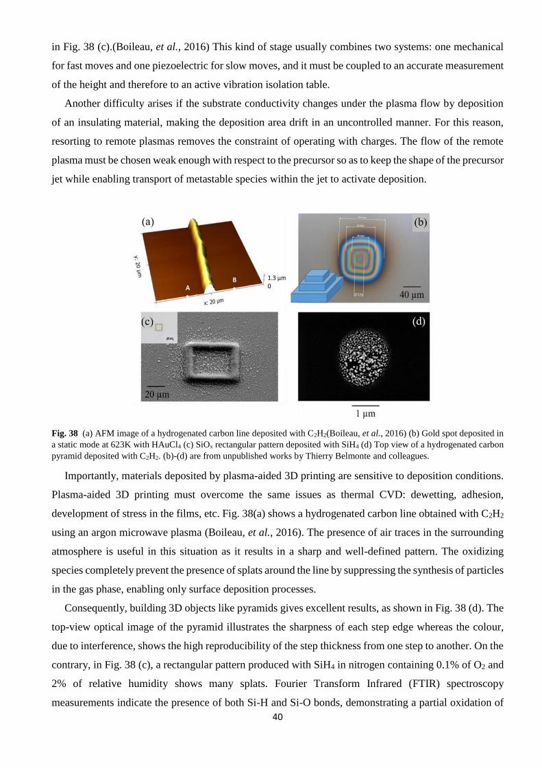
40
in Fig. 38 (c).(Boileau, et al., 2016) This kind of stage usually combines two systems: one mechanical
for fast moves and one piezoelectric for slow moves, and it must be coupled to an accurate measurement
of the height and therefore to an active vibration isolation table.
Another difficulty arises if the substrate conductivity changes under the plasma flow by deposition
of an insulating material, making the deposition area drift in an uncontrolled manner. For this reason,
resorting to remote plasmas removes the constraint of operating with charges. The flow of the remote
plasma must be chosen weak enough with respect to the precursor so as to keep the shape of the precursor
jet while enabling transport of metastable species within the jet to activate deposition.
Fig. 38 (a) AFM image of a hydrogenated carbon line deposited with C2H2(Boileau, et al., 2016) (b) Gold spot deposited in
a static mode at 623K with HAuCl4 (c) SiOx rectangular pattern deposited with SiH4 (d) Top view of a hydrogenated carbon
pyramid deposited with C2H2. (b)-(d) are from unpublished works by Thierry Belmonte and colleagues.
Importantly, materials deposited by plasma-aided 3D printing are sensitive to deposition conditions.
Plasma-aided 3D printing must overcome the same issues as thermal CVD: dewetting, adhesion,
development of stress in the films, etc. Fig. 38(a) shows a hydrogenated carbon line obtained with C2H2
using an argon microwave plasma (Boileau, et al., 2016). The presence of air traces in the surrounding
atmosphere is useful in this situation as it results in a sharp and well-defined pattern. The oxidizing
species completely prevent the presence of splats around the line by suppressing the synthesis of particles
in the gas phase, enabling only surface deposition processes.
Consequently, building 3D objects like pyramids gives excellent results, as shown in Fig. 38 (d). The
top-view optical image of the pyramid illustrates the sharpness of each step edge whereas the colour,
due to interference, shows the high reproducibility of the step thickness from one step to another. On the
contrary, in Fig. 38 (c), a rectangular pattern produced with SiH4 in nitrogen containing 0.1% of O2 and
2% of relative humidity shows many splats. Fourier Transform Infrared (FTIR) spectroscopy
measurements indicate the presence of both Si-H and Si-O bonds, demonstrating a partial oxidation of
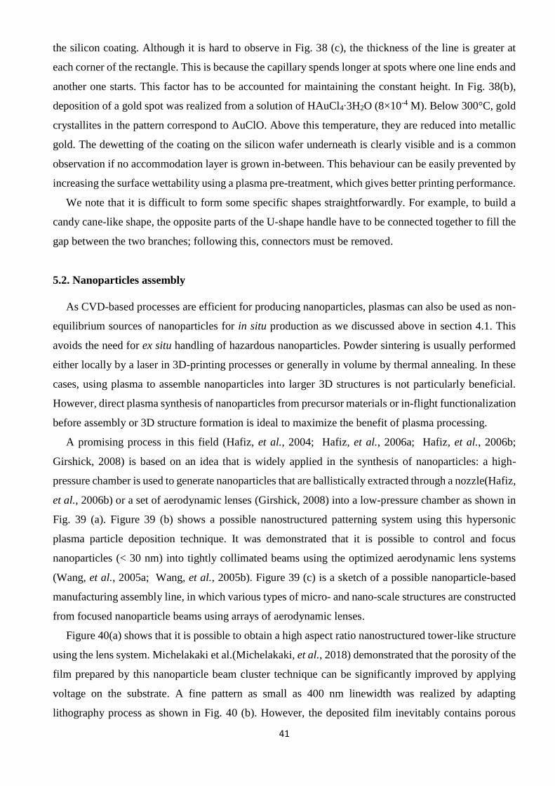
41
the silicon coating. Although it is hard to observe in Fig. 38 (c), the thickness of the line is greater at
each corner of the rectangle. This is because the capillary spends longer at spots where one line ends and
another one starts. This factor has to be accounted for maintaining the constant height. In Fig. 38(b),
deposition of a gold spot was realized from a solution of HAuCl4∙3H2O (8×10⁻⁴ M). Below 300°C, gold
crystallites in the pattern correspond to AuClO. Above this temperature, they are reduced into metallic
gold. The dewetting of the coating on the silicon wafer underneath is clearly visible and is a common
observation if no accommodation layer is grown in-between. This behaviour can be easily prevented by
increasing the surface wettability using a plasma pre-treatment, which gives better printing performance.
We note that it is difficult to form some specific shapes straightforwardly. For example, to build a
candy cane-like shape, the opposite parts of the U-shape handle have to be connected together to fill the
gap between the two branches; following this, connectors must be removed.
5.2. Nanoparticles assembly
As CVD-based processes are efficient for producing nanoparticles, plasmas can also be used as non-
equilibrium sources of nanoparticles for in situ production as we discussed above in section 4.1. This
avoids the need for ex situ handling of hazardous nanoparticles. Powder sintering is usually performed
either locally by a laser in 3D-printing processes or generally in volume by thermal annealing. In these
cases, using plasma to assemble nanoparticles into larger 3D structures is not particularly beneficial.
However, direct plasma synthesis of nanoparticles from precursor materials or in-flight functionalization
before assembly or 3D structure formation is ideal to maximize the benefit of plasma processing.
A promising process in this field (Hafiz, et al., 2004; Hafiz, et al., 2006a; Hafiz, et al., 2006b;
Girshick, 2008) is based on an idea that is widely applied in the synthesis of nanoparticles: a high-
pressure chamber is used to generate nanoparticles that are ballistically extracted through a nozzle(Hafiz,
et al., 2006b) or a set of aerodynamic lenses (Girshick, 2008) into a low-pressure chamber as shown in
Fig. 39 (a). Figure 39 (b) shows a possible nanostructured patterning system using this hypersonic
plasma particle deposition technique. It was demonstrated that it is possible to control and focus
nanoparticles (< 30 nm) into tightly collimated beams using the optimized aerodynamic lens systems
(Wang, et al., 2005a; Wang, et al., 2005b). Figure 39 (c) is a sketch of a possible nanoparticle-based
manufacturing assembly line, in which various types of micro- and nano-scale structures are constructed
from focused nanoparticle beams using arrays of aerodynamic lenses.
Figure 40(a) shows that it is possible to obtain a high aspect ratio nanostructured tower-like structure
using the lens system. Michelakaki et al.(Michelakaki, et al., 2018) demonstrated that the porosity of the
film prepared by this nanoparticle beam cluster technique can be significantly improved by applying
voltage on the substrate. A fine pattern as small as 400 nm linewidth was realized by adapting
lithography process as shown in Fig. 40 (b). However, the deposited film inevitably contains porous
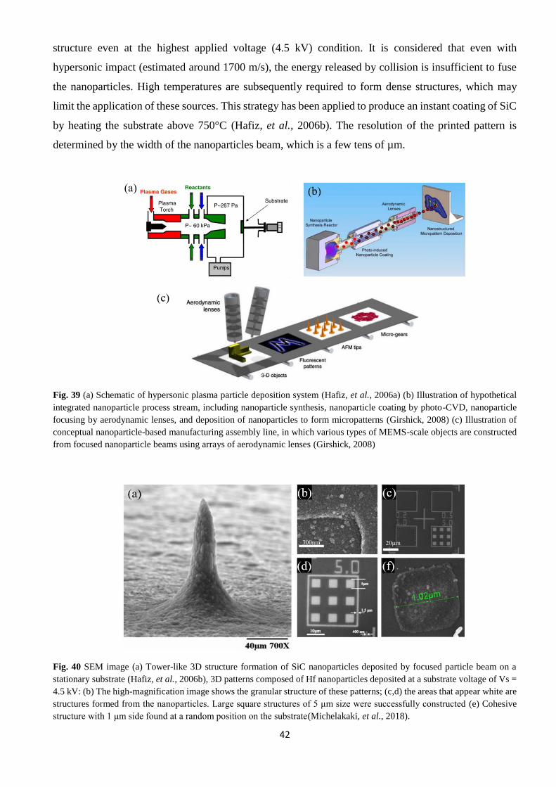
42
structure even at the highest applied voltage (4.5 kV) condition. It is considered that even with
hypersonic impact (estimated around 1700 m/s), the energy released by collision is insufficient to fuse
the nanoparticles. High temperatures are subsequently required to form dense structures, which may
limit the application of these sources. This strategy has been applied to produce an instant coating of SiC
by heating the substrate above 750°C (Hafiz, et al., 2006b). The resolution of the printed pattern is
determined by the width of the nanoparticles beam, which is a few tens of µm.
Fig. 39 (a) Schematic of hypersonic plasma particle deposition system (Hafiz, et al., 2006a) (b) Illustration of hypothetical
integrated nanoparticle process stream, including nanoparticle synthesis, nanoparticle coating by photo-CVD, nanoparticle
focusing by aerodynamic lenses, and deposition of nanoparticles to form micropatterns (Girshick, 2008) (c) Illustration of
conceptual nanoparticle-based manufacturing assembly line, in which various types of MEMS-scale objects are constructed
from focused nanoparticle beams using arrays of aerodynamic lenses (Girshick, 2008)
Fig. 40 SEM image (a) Tower-like 3D structure formation of SiC nanoparticles deposited by focused particle beam on a
stationary substrate (Hafiz, et al., 2006b), 3D patterns composed of Hf nanoparticles deposited at a substrate voltage of Vs =
4.5 kV: (b) The high-magnification image shows the granular structure of these patterns; (c,d) the areas that appear white are
structures formed from the nanoparticles. Large square structures of 5 μm size were successfully constructed (e) Cohesive
structure with 1 μm side found at a random position on the substrate(Michelakaki, et al., 2018).
43
The use of plasma to produce nanoparticles that can be assembled into 3D structures has been
exploited utilizing a nanoxerographic process (Barry, et al., 2003; Barry, et al., 2005). In this process,
localized deposits are formed from nanoparticles that are deflected by a high voltage applied on a
patterned nano-electrode. The plasma is used only as a monodisperse source of charged nanoparticles.
The resolution is spectacular, the deposited patterns having a characteristic dimension of about 100 nm.
Although plasmas has been successfully employed for the in situ production of nanoparticles in 3D
printing processes, there are still obstacles to overcome in this area; in each of the discussed examples,
monodisperse distributions of nanoparticles at given mean size are still required (Hafiz, et al., 2006b).
5.3. Plasma treatment of 3D objects
There are several options for atmospheric-pressure plasma processing of 3D objects. The plasmas can
either be mounted directly on a 3D printer head or used as a post-printing technique to clean,
functionalize or reduce the roughness of surfaces. A few representative examples are discussed below.
The Flashfuse filament technology is a 3D printing solution commercialized by Essentium,
Inc.(Essentium) as we briefly introduced in section 1. The polymer or composite to be deposited is
introduced through a nozzle in the centre of a conductor disk positioned above the grounded 3D printed
part to be built. Within the gap between the two surfaces, an air plasma is ignited. The whole system is
heated to improve the interface exchange mechanisms. Therefore, the issue of delamination, which
usually plagues pieces formed by conventional fused deposition discussed in section 2, is solved.
Filaments, made of Polyether Ether Ketone (PEEK) or carbon fibre reinforced polymers for instance,
are coated with conductive carbon nanotubes to weld each printed cross section to the previously printed
layers. By addressing the bonding of the polymer chains at the nanoscale level, larger heat affected zones
are created, thereby improving the strength of the cross-sectional welds and the resulting strength of the
parts. A result of this is that polymer chains can better migrate and entangle. This technology was
mentioned in relation to building the solar cell umbrellas that are expected to provide long-term
photovoltaic power on Mars (Adams, et al., 2018).
Another example is the PDD® Plasma technology (Piezoelectric Direct Discharge) by Relyon Plasma
which can be integrated directly into 3D printers (Plasma). A voltage supply of 15 V is needed for the
compact plasma module (piezobrush® PZ2), which typically has a power consumption of less than 15
W. In typical applications on the basis of conventional FDM technology, this simple system can change
the surface wettability of the deposited polymer, leading to the improvements in the gluing or painting
steps.
As we discussed earlier, it is also possible to directly deposit other nanomaterials such as carbon
nanotubes or nanogold (Gandhiraman, et al., 2016),(Hong, et al., 2019). A low-temperature plasma jet
44
with emulsion of nanoparticle or solution-based precursor supply can be effective to coat 3-D objects
and flexible surfaces, such as paper or cloth, with a functional nanomaterial or even composite.
Plasma-modified polymers used as a scaffold for biomedical applications have been intensively
studied (Cools, et al., 2018; Joshy, et al., 2019). Indeed, surface modification using plasmas is a highly
exploited and productive technique in tissue engineering and regenerative medicine. Plasma
modification is known to improve surface properties and thereby enhance the biocompatibility of the
materials involved. As we earlier mentioned in section 1, Fraunhofer Institute for Applied Polymer
Research (IAP) and Thin Films (IST) developed a plasma jet technique for 3D Printing customized bone
implants, which couples both aspects – plasma treatment and 3D printing – in a single solution
(Fraunhofer, 2018). The device blows a cold jet of plasma containing reactive groups directly onto the
3D printed layers. Amino groups present in the precursor bond with the surface and ensure adhesion of
bone cells to the substrate. No chemical pre-treatment with solvents is required for the coating, so the
procedure is both cost-effective and environmentally friendly. Wang et al. (Wang, et al., 2016b) showed
that cold atmospheric plasmas modify the nanoscale roughness and chemical composition of a 3D
printed poly-lactic-acid scaffold surface, thus promoting both osteoblast (bone forming cells) and
mesenchymal stem cell attachment and proliferation.
Perelaer et al. (Perelaer, et al., 2012) developed a mixed system combining plasma and microwave
flash sintering to sinter an inkjet‐printed and tailored silver nanoparticle formulation. The processing
temperature remains well below the glass transition temperature of the used polymer substrate. This
approach leads to highly conductive features, which are compatible with R2R but also with 3D-printing
production.
6. Outlook and Conclusion
It is evident that low-temperature, atmospheric-pressure plasmas can play an impactful role in
additive manufacturing and other areas of advanced digital manufacturing. The recent parallel
development of both 3D printing and atmospheric plasma technologies offers the feasibility to combine
the approaches with a view to producing new and highly controlled materials, structures, and devices.
The diverse nature of the physics and chemistry of plasmas and their multi-modal effects means that
there is a vast array of operational variables which need to be examined and optimised for specific AM
applications. Compounding this complexity is the continued evolution of multi-material additive
manufacturing (MM-AM) which offers complex multi-component products. The behaviour of different
materials as they interface with both each other and the plasma during the printing process needs to be
understood. As outlined in this paper, there are numerous integration approaches for combining the
technologies which need to be classified and ideally standardised for plasma printing. Integration of
plasma sources need to not only take into consideration the ease of combining the printing process with
45
the discharge but to also the plasma induced effects which may influence the process such as gas flow
effects, reactive chemistry with the surrounding atmosphere, and other factors.
The ability to effectively scale the process is a key challenge, particularly where large volumes or
dimensions are sought with features that are set to a micro or indeed nano-scale level. The time-scale of
these processes should also be considered and matched with the induced reactions.
Given the scales and resolution required by advanced manufacturing, effective control of the plasma-
printing process is required. Non-invasive and real-time plasma diagnostic techniques could be
integrated within the plasma-printing process to provide both mechanistic insights, process tuning and
control. The potential to link high resolution imaging of the printing process to plasma data would
provide useful information to drive technology evolution in this space.
It is clear from the rapidly emerging literature and indeed the few commercial offerings on the market
that the integration of non-thermal plasmas with printing processes is an active area of research with a
wide range of potential end applications. The combination of plasma and 3D printing has the potential
to transform processes across a wide range of industries, creating products that significantly enhance
both science and society.
Many limitations of current processes can be overcome by combining plasma with 3D printing.
However, these techniques are still in their early days and require further research to improve and expand
their use. This is why we sincerely hope that our effort to critically examine the recent progress and
potential of atmospheric-pressure plasmas, and plasma nanotechnology in particular, to help advance
the rapidly developing digital manufacturing – the technology which is poised to sustain the next
industrial revolution in the digital manufacturing age – will stimulate information exchange and
collaborative efforts among the scientists and engineers normally working in disparate fields.
Acknowledgments
We sincerely acknowledge the efforts of all researchers who have worked in any of the relevant areas
and apologize if any of relevant works were not included due to specific focus and length limits of this
article. This work was performed under the CSIRO-QUT Joint Laboratories Agreement. J. H. and B. A.
gratefully acknowledge funding by the CSIRO Research Plus Postdoctoral Fellowship scheme. P. J. C.
and K. O. thank the Australian Research Council for partial support.
46
REFERENCES
Press release. Fraunhofer Institute for Applied Polymer Research IAP and Thin Films IST
https://www.fraunhofer.de/content/dam/zv/en/press-media/2018/december/research-news/rn12-2018-IST-
precisely-fitting-bone-implants-from-the-printer.pdf
L. Abhinandan, and A. Hollander, Localized deposition of hydrocarbon using plasma activated chemical vapour
deposition, Thin Solid Films 457, 241-245 (2004)
G. Adams, J. Banks, C. Frazier, U. Toodi, and M. Lagoudas, 2018, in (Texas A&M University).
J. Alaman, R. Alicante, J. I. Pena, and C. Sanchez-Somolinos, Inkjet Printing of Functional Materials for Optical
and Photonic Applications, Materials 9, 910 (2016)
R. J. Anthony, K. Y. Cheng, Z. C. Holman, R. J. Holmes, and U. R. Kortshagen, An All-Gas-Phase Approach for
the Fabrication of Silicon Nanocrystal Light-Emitting Devices, Nano Lett. 12, 2822-2825 (2012)
I. Bahnini, M. Rivette, A. Rechia, A. Siadat, and A. Elmesbahi, Additive manufacturing technology: the status,
applications, and prospects, Int J Adv Manuf Tech 97, 147-161 (2018)
C. R. Barry, J. Gu, and H. O. Jacobs, Charging process and coulomb-force-directed printing of nanoparticles with
sub-100-nm lateral resolution, Nano Lett. 5, 2078-2084 (2005)
C. R. Barry, N. Z. Lwin, W. Zheng, and H. O. Jacobs, Printing nanoparticle building blocks from the gas phase
using nanoxerography, Appl. Phys. Lett. 83, 5527-5529 (2003)
T. Belmonte, T. Gries, R. P. Cardoso, G. Arnoult, F. Kosior, and G. Henrion, Chemical vapour deposition
enhanced by atmospheric microwave plasmas: a large-scale industrial process or the next
nanomanufacturing tool?, Plasma Sources Sci T 20, 024004 (2011)
T. Belmonte, G. Henrion, and T. Gries, Nonequilibrium Atmospheric Plasma Deposition, J. Therm. Spray
Technol. 20, 744-759 (2011)
J. P. Boeuf, Y. Lagmich, T. Unfer, T. Callegari, and L. C. Pitchford, Electrohydrodynamic force in dielectric
barrier discharge plasma actuators, Journal of Physics D-Applied Physics 40, 652-662 (2007)
A. Boileau, T. Gries, C. Noel, R. P. Cardoso, and T. Belmonte, Sub-micro a-C:H patterning of silicon surfaces
assisted by atmospheric-pressure plasma-enhanced chemical vapor deposition, Journal of Physics D-
Applied Physics 49, 445306 (2016)
A. Botman, J. J. L. Mulders, and C. W. Hagen, Creating pure nanostructures from electron-beam-induced
deposition using purification techniques: a technology perspective, Nanotechnology 20, 372001 (2009)
M. I. Boulos, The Role of Transport Phenomena and Modeling in the Development of Thermal Plasma
Technology, Plasma Chem. Plasma Process. 36, 3-28 (2016)
T. Bret, I. Utke, C. Gaillard, and P. Hoffmann, Periodic structure formation by focused electron-beam-induced
deposition, Journal of Vacuum Science & Technology B 22, 2504-2510 (2004)
D. Chakravarty, C. S. Tiwary, C. F. Woellner, S. Radhakrishnan, S. Vinod, S. Ozden, P. A. D. Autreto, S.
Bhowmick, S. Asif, S. A. Mani, et al., 3D Porous Graphene by Low-Temperature Plasma Welding for Bone
Implants, Advanced Materials 28, 8959-8967 (2016)
K. Cheng, M. H. Yang, W. W. W. Chiu, C. Y. Huang, J. Chang, T. F. Ying, and Y. Yang, Ink-jet printing, self-
assembled polyelectrolytes, and electroless plating: Low cost fabrication of circuits on a flexible substrate
at room temperature, Macromol. Rapid Commun. 26, 247-264 (2005)
J. W. Choi, E. MacDonald, and R. Wicker, Multi-material microstereolithography, Int J Adv Manuf Tech 49, 543-
551 (2010)
L. Chong, S. Ramakrishna, and S. Singh, A review of digital manufacturing-based hybrid additive manufacturing
processes, Int J Adv Manuf Tech 95, 2281-2300 (2018)
A. Clausen, F. W. Wang, J. S. Jensen, O. Sigmund, and J. A. Lewis, Topology Optimized Architectures with
Programmable Poisson's Ratio over Large Deformations, Advanced Materials 27, 5523-5527 (2015)
P. Cools, C. Mota, I. Lorenzo-Moldero, R. Ghobeira, N. De Geyter, L. Moroni, and R. Morent, Acrylic Acid
Plasma Coated 3D Scaffolds for Cartilage tissue engineering applications, Sci. Rep. 8, 3830 (2018)
E. A. Corbin, L. J. Millet, J. H. Pikul, C. L. Johnson, J. G. Georgiadis, W. P. King, and R. Bashir, Micromechanical
properties of hydrogels measured with MEMS resonant sensors, Biomed. Microdevices 15, 311-319 (2013)
R. d'Agostino, P. Favia, C. Oehr, and M. R. Wertheimer, Low-temperature plasma processing of materials: Past,
present, and future, Plasma Process Polym 2, 7-15 (2005)
B. J. de Gans, P. C. Duineveld, and U. S. Schubert, Inkjet printing of polymers: State of the art and future
developments, Advanced Materials 16, 203-213 (2004)
47
T. DebRoy, H. L. Wei, J. S. Zuback, T. Mukherjee, J. W. Elmer, J. O. Milewski, A. M. Beese, A. Wilson-Heid,
A. De, and W. Zhang, Additive manufacturing of metallic components - Process, structure and properties,
Prog. Mater Sci. 92, 112-224 (2018)
A. Dey, S. Krishnamurthy, J. Bowen, D. Nordlund, M. Meyyappan, and R. P. Gandhiraman, Plasma Jet Printing
and in Situ Reduction of Highly Acidic Graphene Oxide, ACS Nano 12, 5473-5481 (2018)
Essentium, http://essentium3d.com
H. Exner, M. Horn, A. Streek, P. Regenfuss, F. Ullmann, and R. Ebert, Laser Micro Sintering - A new method to
generate metal and ceramic parts of high resolution with sub-micrometer powder, Virtual and Physical
Prototyping 3, 3-11 (2008)
R. D. Farahani, M. Dube, and D. Therriault, Three-Dimensional Printing of Multifunctional Nanocomposites:
Manufacturing Techniques and Applications, Advanced Materials 28, 5794-5821 (2016)
S. Felton, M. Tolley, E. Demaine, D. Rus, and R. Wood, A method for building self-folding machines, Science
345, 644-646 (2014)
S. R. Forrest, The path to ubiquitous and low-cost organic electronic appliances on plastic, Nature 428, 911-918
(2004)
H. Forster, C. Wolfrum, and W. Peukert, Experimental study of metal nanoparticle synthesis by an arc
evaporation/condensation process, J. Nanopart. Res. 14, 926 (2012)
J. D. Fowlkes, R. Winkler, B. B. Lewis, M. G. Stanford, H. Plank, and P. D. Rack, Simulation-Guided 3D
Nanomanufacturing via Focused Electron Beam Induced Deposition, Acs Nano 10, 6163-6172 (2016)
K. Fricke, H. Steffen, T. von Woedtke, K. Schroder, and K. D. Weltmann, High Rate Etching of Polymers by
Means of an Atmospheric Pressure Plasma Jet, Plasma Process Polym 8, 51-58 (2011)
A. Frutiger, J. T. Muth, D. M. Vogt, Y. Menguc, A. Campo, A. D. Valentine, C. J. Walsh, and J. A. Lewis,
Capacitive Soft Strain Sensors via Multicore-Shell Fiber Printing, Advanced Materials 27, 2440-2446
(2015)
P. Galliker, J. Schneider, H. Eghlidi, S. Kress, V. Sandoghdar, and D. Poulikakos, Direct printing of
nanostructures by electrostatic autofocussing of ink nanodroplets, Nat Commun 3, 890 (2012)
R. P. Gandhiraman, E. Singh, D. C. Diaz-Cartagena, D. Nordlund, J. Koehne, and M. Meyyappan, Plasma jet
printing for flexible substrates, Appl. Phys. Lett. 108, 123103 (2016)
M. Gavagnin, H. D. Wanzenboeck, S. Wachter, M. M. Shawrav, A. Persson, K. Gunnarsson, P. Svedlindh, M.
Stoger-Pollach, and E. Bertagnolli, Free-Standing Magnetic Nanopillars for 3D Nanomagnet Logic, Acs
Appl Mater Inter 6, 20254-20260 (2014)
H. C. George, T. A. Orlova, A. O. Orlov, and G. L. Snider, Novel method for fabrication of nanoscale single-
electron transistors: Electron beam induced deposition of Pt and atomic layer deposition of tunnel barriers,
Journal of Vacuum Science & Technology B 29, 06FB01 (2011)
M. K. Ghatkesar, H. H. P. Garza, F. Heuck, and U. Staufer, Scanning Probe Microscope-Based Fluid Dispensing,
Micromachines 5, 954-1001 (2014)
S. L. Girshick, Aerosol processing for nanomanufacturing, J. Nanopart. Res. 10, 935-945 (2008)
A. S. Gladman, E. A. Matsumoto, R. G. Nuzzo, L. Mahadevan, and J. A. Lewis, Biomimetic 4D printing, Nat
Mater 15, 413 (2016)
N. Y. M. Gonzalez, M. El Morsli, and P. Proulx, Production of Nanoparticles in Thermal Plasmas: A Model
Including Evaporation, Nucleation, Condensation, and Fractal Aggregation, J. Therm. Spray Technol. 17,
533-550 (2008)
P. Grenson, O. Leon, P. Reulet, and B. Aupoix, Investigation of an impinging heated jet for a small nozzle-to-
plate distance and high Reynolds number: An extensive experimental approach, Int. J. Heat Mass Transfer
102, 801-815 (2016)
D. J. Guo, R. Kometani, S. Warisawa, and S. Ishihara, Growth of ultra-long free-space-nanowire by the real-time
feedback control of the scanning speed on focused-ion-beam chemical vapor deposition, Journal of Vacuum
Science & Technology B 31, 061601 (2013)
J. Y. Guo, X. B. Fan, R. Dolbec, S. W. Xue, J. Jurewicz, and M. Boulos, Development of Nanopowder Synthesis
Using Induction Plasma, Plasma Sci Technol 12, 188-199 (2010)
J. Hafiz, R. Mukherjee, X. Wang, J. V. R. Heberlein, P. H. McMurry, and S. L. Girshick, Analysis of
nanostructured coatings synthesized by ballistic impaction of nanoparticles, Thin Solid Films 515, 1147-
1151 (2006)
J. Hafiz, R. Mukherjee, X. Wang, P. H. McMurry, J. V. R. Heberlein, and S. L. Girshick, Hypersonic plasma
particle deposition - A hybrid between plasma spraying and vapor deposition, J. Therm. Spray Technol. 15,
822-826 (2006)
48
J. Hafiz, X. Wang, R. Mukherjee, W. Mook, C. R. Perrey, J. Deneen, J. V. R. Heberlein, P. H. McMurry, W. W.
Gerberich, C. B. Carter, et al., Hypersonic plasma particle deposition of Si-Ti-N nanostructured coatings,
Surf Coat Tech 188, 364-370 (2004)
H. Hartl, Y. R. Guo, K. Ostrikov, Y. B. Xian, J. Zheng, X. G. Li, K. E. Fairfull-Smith, and J. MacLeod, Film
formation from plasma-enabled surface-catalyzed dehalogenative coupling of a small organic molecule,
Rsc Adv 9, 2848-2856 (2019)
D. Herzog, V. Seyda, E. Wycisk, and C. Emmelmann, Additive manufacturing of metals, Acta Mater. 117, 371-
392 (2016)
L. Hirt, A. Reiser, R. Spolenak, and T. Zambelli, Additive Manufacturing of Metal Structures at the Micrometer
Scale, Advanced Materials 29, 1604211 (2017)
A. Hollander, and L. Abhinandan, Localized deposition by mu-jet-CVD, Surf Coat Tech 174, 1175-1177 (2003)
J. Hong, S. Yick, E. Chow, A. Murdock, J. Fang, D. H. Seo, A. Wolff, Z. Han, T. van der Laan, A. Bendavid, et
al., Direct plasma printing of nano-gold from an inorganic precursor, J Mater Chem C 7, 6369 (2019)
J. L. Hu, H. P. Meng, G. Q. Li, and S. I. Ibekwe, A review of stimuli-responsive polymers for smart textile
applications, Smart Mater. Struct. 21, 053001 (2012)
K. I. Hunter, J. T. Held, K. A. Mkhoyan, and U. R. Kortshagen, Nonthermal Plasma Synthesis of Core/Shell
Quantum Dots: Strained Ge/Si Nanocrystals, Acs Appl Mater Inter 9, 8263-8270 (2017)
Innophysics, http://www.innophysics.nl/index.php/projects/plasmaprint-ald
E. Jager, J. Schmidt, A. Pfuch, S. Spange, O. Beier, N. Jager, O. Jantschner, R. Daniel, and C. Mitterer,
Antibacterial Silicon Oxide Thin Films Doped with Zinc and Copper Grown by Atmospheric Pressure
Plasma Chemical Vapor Deposition, Nanomaterials-Basel 9, 255 (2019)
P. I. John, Plasma Sciences and the Creation of Wealth (Tata McGraw Hill Education, New York City, 2005)
K. S. Joshy, S. Snigdha, and S. Thomas, Plasma Modified Polymeric Materials for Scaffolding of Bone Tissue
Engineering (Elsevier, Amsterdam, 2019)
K. S. Kim, and T. H. Kim, Nanofabrication by thermal plasma jets: From nanoparticles to low-dimensional
nanomaterials, J. Appl. Phys. 125, 070901 (2019)
D. B. Kolesky, R. L. Truby, A. S. Gladman, T. A. Busbee, K. A. Homan, and J. A. Lewis, 3D Bioprinting of
Vascularized, Heterogeneous Cell-Laden Tissue Constructs, Advanced Materials 26, 3124-3130 (2014)
H. W. P. Koops, O. E. Hoinkis, M. E. W. Honsberg, R. Schmidt, R. Blum, G. Bottger, A. Kuligk, C. Liguda, and
M. Eich, Two-dimensional photonic crystals produced by additive nanolithography with electron beam-
induced deposition act as filters in the infrared, Microelectron. Eng. 57-8, 995-1001 (2001)
U. Kortshagen, and U. Bhandarkar, Modeling of particulate coagulation in low pressure plasmas, Phys Rev E 60,
887-898 (1999)
U. R. Kortshagen, R. M. Sankaran, R. N. Pereira, S. L. Girshick, J. J. Wu, and E. S. Aydil, Nonthermal Plasma
Synthesis of Nanocrystals: Fundamental Principles, Materials, and Applications, Chem. Rev. 116, 11061-
11127 (2016)
F. Kotz, K. Arnold, W. Bauer, D. Schild, N. Keller, K. Sachsenheimer, T. M. Nargang, C. Richter, D. Helmer,
and B. E. Rapp, Three-dimensional printing of transparent fused silica glass, Nature 544, 337 (2017)
N. J. Kramer, R. J. Anthony, M. Mamunuru, E. S. Aydil, and U. R. Kortshagen, Plasma-induced crystallization
of silicon nanoparticles, Journal of Physics D-Applied Physics 47, 075202 (2014)
N. J. Kramer, E. S. Aydil, and U. R. Kortshagen, Requirements for plasma synthesis of nanocrystals at
atmospheric pressures, Journal of Physics D-Applied Physics 48, 035205 (2015)
A. Kumar, S. Kang, C. Larriba-Andaluz, H. Ouyang, C. J. Hogan, and R. M. Sankaran, Ligand-free Ni nanocluster
formation at atmospheric pressure via rapid quenching in a microplasma process, Nanotechnology 25,
(2014)
S. Kyung, Y. Lee, C. Kim, J. Lee, and G. Yeom, Deposition of carbon nanotubes by capillary-type atmospheric
pressure PECVD, Thin Solid Films 506, 268-273 (2006)
A. Lazea-Stoyanova, A. Vlad, A. M. Vlaicu, V. S. Teodorescu, and G. Dinescu, Synthesis of Copper Particles by
Non-thermal Atmospheric Pressure Plasma Jet, Plasma Process Polym 12, 705-709 (2015)
H. H. Lee, K. S. Chou, and K. C. Huang, Inkjet printing of nanosized silver colloids, Nanotechnology 16, 2436-
2441 (2005)
S. W. Lee, D. Liang, X. P. A. Gao, and R. M. Sankaran, Direct Writing of Metal Nanoparticles by Localized
Plasma Electrochemical Reduction of Metal Cations in Polymer Films, Adv. Funct. Mater. 21, 2155-2161
(2011)
B. B. Lewis, M. G. Stanford, J. D. Fowlkes, K. Lester, H. Plank, and P. D. Rack, Electron-stimulated purification
of platinum nanostructures grown via focused electron beam induced deposition, Beilstein J Nanotech 6,
907-918 (2015)
J. A. Lewis, Direct ink writing of 3D functional materials, Adv. Funct. Mater. 16, 2193-2204 (2006)
49
M. M. Ling, and Z. N. Bao, Thin film deposition, patterning, and printing in organic thin film transistors, Chem.
Mater. 16, 4824-4840 (2004)
Y. Liu, J. K. Boyles, J. Genzer, and M. D. Dickey, Self-folding of polymer sheets using local light absorption,
Soft Matter 8, 1764-1769 (2012)
M. F. Mabrook, C. Pearson, A. S. Jombert, D. A. Zeze, and M. C. Petty, The morphology, electrical conductivity
and vapour sensing ability of inkjet-printed thin films of single-wall carbon nanotubes, Carbon 47, 752-757
(2009)
K. Mackie, and M. Gordon, Microplasma-based deposition of functional nanomaterials for energy storage
applications, Abstracts of Papers of The American Chemical Society 253, Apr 2, (2017)
K. E. Mackie, A. C. Pebley, M. M. Butala, J. P. Zhang, G. D. Stucky, and M. J. Gordon, Microplasmas for direct,
substrate-independent deposition of nanostructured metal oxides, Appl. Phys. Lett. 109, 033110 (2016)
S. Magdassi, A. Bassa, Y. Vinetsky, and A. Kamyshny, Silver nanoparticles as pigments for water-based ink-jet
inks, Chem. Mater. 15, 2208-2217 (2003)
P. Maguire, D. Rutherford, M. Macias-Montero, C. Mahony, C. Kelsey, M. Tweedie, F. Perez-Martin, H.
McQuaid, D. Diver, and D. Mariottit, Continuous In-Flight Synthesis for On-Demand Delivery of Ligand-
Free Colloidal Gold Nanoparticles, Nano Lett. 17, 1336-1343 (2017)
R. M. Mahamood, Laser Metal Deposition Process of Metals, Alloys, and Composite Materials (Springer,
International, 2018)
A. Mameli, Y. H. Kuang, M. Aghaee, C. K. Ande, B. Karasulu, M. Creatore, A. J. M. Mackus, W. M. M. Kessels,
and F. Roozeboornt, Area-Selective Atomic Layer Deposition of In2O3:H Using a μ-Plasma Printer for
Local Area Activation, Chem. Mater. 29, 921-925 (2017)
L. Mangolini, and U. Kortshagen, Plasma-assisted synthesis of silicon nanocrystal inks, Advanced Materials 19,
2513-2519 (2007)
L. Mangolini, E. Thimsen, and U. Kortshagen, High-yield plasma synthesis of luminescent silicon nanocrystals,
Nano Lett. 5, 655-659 (2005)
Y. Q. Mao, K. Yu, M. S. Isakov, J. T. Wu, M. L. Dunn, and H. J. Qi, Sequential Self-Folding Structures by 3D
Printed Digital Shape Memory Polymers, Sci. Rep. 5, 13616 (2015)
T. Matsoukas, and M. Russell, Particle Charging in Low-Pressure Plasmas, J. Appl. Phys. 77, 4285-4292 (1995)
R. Maurau, N. D. Boscher, S. Olivier, S. Bulou, T. Belmonte, J. Dutroncy, T. Sindzingre, and P. Choquet,
Atmospheric pressure, low temperature deposition of photocatalytic TiOx thin films with a blown arc
discharge, Surf Coat Tech 232, 159-165 (2013)
I. Michelakaki, N. Boukos, D. A. Dragatogiannis, S. Stathopoulos, C. A. Charitidis, and D. Tsoukalas, Synthesis
of hafnium nanoparticles and hafnium nanoparticle films by gas condensation and energetic deposition,
Beilstein J Nanotech 9, 1868-1880 (2018)
S. Y. Min, T. S. Kim, B. J. Kim, H. Cho, Y. Y. Noh, H. Yang, J. H. Cho, and T. W. Lee, Large-scale organic
nanowire lithography and electronics, Nat Commun 4, 1773 (2013)
S. Mohr, and O. Khan, 3D Printing and Its Disruptive Impacts on Supply Chains of the Future, Technol Innov
Manag 20-25 (2015)
I. Motrescu, and M. Nagatsu, Nanocapillary Atmospheric Pressure Plasma Jet: A Tool for Ultrafine Maskless
Surface Modification at Atmospheric Pressure, Acs Appl Mater Inter 8, 12528-12533 (2016)
K. Murakami, and M. Takai, Nano electron source fabricated by beam-induced deposition and its unique feature,
Microelectron. Eng. 132, 74-82 (2015)
L. E. Murr, S. M. Gaytan, D. A. Ramirez, E. Martinez, J. Hernandez, K. N. Amato, P. W. Shindo, F. R. Medina,
and R. B. Wicker, Metal Fabrication by Additive Manufacturing Using Laser and Electron Beam Melting
Technologies, Journal of Materials Science & Technology 28, 1-14 (2012)
T. J. Ober, D. Foresti, and J. A. Lewis, Active mixing of complex fluids at the microscale, Proc. Natl. Acad. Sci.
U.S.A. 112, 12293-12298 (2015)
S. Ohno, and M. Uda, Preparation for Ultrafine Particles of Fe-Ni, Fe-Cu and Fe-Si Alloys by Hydrogen Plasma-
Metal Reaction, J. Jpn. Inst. Met. 53, 946-952 (1989)
R. Parashkov, E. Becker, T. Riedl, H. H. Johannes, and W. Kowalsky, Large area electronics using printing,
methods, Proceedings of the Ieee 93, 1321-1329 (2005)
J.-U. Park, M. Hardy, S. J. Kang, K. Barton, K. Adair, D. k. Mukhopadhyay, C. Y. Lee, M. S. Strano, A. G.
Alleyne, J. G. Georgiadis, et al., High-resolution electrohydrodynamic jet printing, Nat Mater 6, 782 (2007)
S. Park, U. Cvelbar, W. Choe, and S. Y. Moon, The creation of electric wind due to the electrohydrodynamic
force, Nat Commun 9, 371 (2018)
J. Perelaer, R. Jani, M. Grouchko, A. Kamyshny, S. Magdassi, and U. S. Schubert, Plasma and Microwave Flash
Sintering of a Tailored Silver Nanoparticle Ink, Yielding 60% Bulk Conductivity on Cost- Effective
Polymer Foils, Advanced Materials 24, 3993-3998 (2012)
50
H. Plank, C. Gspan, M. Dienstleder, G. Kothleitner, and F. Hofer, The influence of beam defocus on volume
growth rates for electron beam induced platinum deposition, Nanotechnology 19, 485302 (2008)
Relyon Plasma, https://www.relyon-plasma.com/maximum-surface-quality-in-3d-printing/?lang=en.
P. D. Rack, J. D. Fowlkes, and S. J. Randolph, In situ probing of the growth and morphology in electron-beam-
induced deposited nanostructures, Nanotechnology 18, 465602 (2007)
C. L. Randall, E. Gultepe, and D. H. Gracias, Self-folding devices and materials for biomedical applications,
Trends Biotechnol. 30, 138-146 (2012)
C. Richmonds, and R. M. Sankaran, Plasma-liquid electrochemistry: Rapid synthesis of colloidal metal
nanoparticles by microplasma reduction of aqueous cations, Appl. Phys. Lett. 93, 131501 (2008)
C. Richmonds, M. Witzke, B. Bartling, S. W. Lee, J. Wainright, C. C. Liu, and R. M. Sankaran, Electron-Transfer
Reactions at the Plasma-Liquid Interface, J. Am. Chem. Soc. 133, 17582-17585 (2011)
P. Richner, S. J. P. Kress, D. J. Norris, and D. Poulikakos, Charge effects and nanoparticle pattern formation in
electrohydrodynamic NanoDrip printing of colloids, Nanoscale 8, 6028-6034 (2016)
S. Sanaur, A. Whalley, B. Alameddine, M. Carnes, and C. Nuckolls, Jet-printed electrodes and semiconducting
oligomers for elaboration of organic thin-film transistors, Org. Electron. 7, 423-427 (2006)
V. Satulu, M. D. Ionita, S. Vizireanu, B. Mitu, and G. Dinescu, Plasma Processing with Fluorine Chemistry for
Modification of Surfaces Wettability, Molecules 21, 1711 (2016)
J. Schneider, P. Rohner, D. Thureja, M. Schmid, P. Galliker, and D. Poulikakos, Electrohydrodynamic NanoDrip
Printing of High Aspect Ratio Metal Grid Transparent Electrodes, Adv. Funct. Mater. 26, 833-840 (2016)
M. Schwentenwein, and J. Homa, Additive Manufacturing of Dense Alumina Ceramics, Int J Appl Ceram Tec
12, 1-7 (2015)
C. W. Sele, T. von Werne, R. H. Friend, and H. Sirringhaus, Lithography-free, self-aligned inkjet printing with
sub-hundred-nanometer resolution, Advanced Materials 17, 997-1001 (2005)
J. H. Seo, and B. G. Hong, Thermal Plasma Synthesis of Nano-Sized Powders, Nucl Eng Technol 44, 9-20 (2012)
S. K. Seol, D. Kim, S. Lee, J. H. Kim, W. S. Chang, and J. T. Kim, Electrodeposition-based 3D Printing of
Metallic Microarchitectures with Controlled Internal Structures, Small 11, 3896-3902 (2015)
M. Shigeta, and A. B. Murphy, Thermal plasmas for nanofabrication, Journal of Physics D-Applied Physics 44,
174025 (2011)
Y. Shimizu, Diameter control of gold nanoparticles synthesized in gas phase using atmospheric-pressure H2/Ar
plasma jet and gold wire as the nanoparticle source: Control by varying the H2/Ar mixture ratio, AIP Adv
7, 015316 (2017)
Y. Shimizu, K. Kawaguchi, T. Sasaki, and N. Koshizaki, Generation of room-temperature atmospheric H2/Ar
microplasma jet driven with pulse-modulated ultrahigh frequency and its application to gold nanoparticle
preparation, Appl. Phys. Lett. 94, 191504 (2009)
Y. Shimizu, T. Sasaki, T. Ito, K. Terashima, and N. Koshizaki, Fabrication of spherical carbon via UHF
inductively coupled microplasma CVD, Journal of Physics D-Applied Physics 36, 2940-2944 (2003)
K. Silmy, A. Hollander, A. Dillmann, and J. Thomel, Micro-jet plasma CVD with HMDSO/O2, Surf Coat Tech
200, 368-371 (2005)
H. Sirringhaus, T. Kawase, R. H. Friend, T. Shimoda, M. Inbasekaran, W. Wu, and E. P. Woo, High-resolution
inkjet printing of all-polymer transistor circuits, Science 290, 2123-2126 (2000)
M. A. Skylar-Scott, S. Gunasekaran, and J. A. Lewis, Laser-assisted direct ink writing of planar and 3D metal
architectures, Proc. Natl. Acad. Sci. U.S.A. 113, 6137-6142 (2016)
M. G. Stanford, B. B. Lewis, J. H. Noh, J. D. Fowlkes, and P. D. Rack, Inert Gas Enhanced Laser-Assisted
Purification of Platinum Electron-Beam-Induced Deposits, Acs Appl Mater Inter 7, 19579-19588 (2015)
A. R. Studart, Additive manufacturing of biologically-inspired materials, Chem. Soc. Rev. 45, 359-376 (2016)
N. Stutzmann, R. H. Friend, and H. Sirringhaus, Self-aligned, vertical-channel, polymer field-effect transistors,
Science 299, 1881-1884 (2003)
Y. Sui, Y. Dai, C. C. Liu, R. M. Sankaran, and C. A. ZormanSui, A New Class of Low-Temperature Plasma-
Activated, Inorganic Salt-Based Particle-Free Inks for Inkjet Printing Metals, Advanced Materials
Technology 1900119 (2019)
J. B. Szczech, C. M. Megaridis, D. R. Gamota, and J. Zhang, Fine-line conductor manufacturing using drop-on-
demand PZT printing technology, Ieee T Electron Pack 25, 26-33 (2002)
T. Takai, H. Nakao, and F. Iwata, Three-dimensional microfabrication using local electrophoresis deposition and
a laser trapping technique, Opt. Express 22, 28109-28117 (2014)
V. Tasco, M. Esposito, F. Todisco, A. Benedetti, M. Cuscuna, D. Sanvitto, and A. Passaseo, Three-dimensional
nanohelices for chiral photonics, Appl Phys A 122, 280 (2016)
EMPA Materials Science and Technology, http://www.empa.ch
Tekna, http://www.tekna.com
51
M. Thomas, J. Borris, A. Dohse, M. Eichler, A. Hinze, K. Lachmann, K. Nagel, and C. P. Klages, Plasma Printing
and Related Techniques - Patterning of Surfaces Using Microplasmas at Atmospheric Pressure, Plasma
Process Polym 9, 1086-1103 (2012)
M. Thomson, J. L. Hodgkinson, and D. W. Sheel, Control of zinc oxide surface structure using combined
atmospheric pressure-based CVD growth and plasma etching, Surf Coat Tech 230, 190-195 (2013)
S. Tibbits, 4d Printing: Multi-Material Shape Change, Archit Design 84, 116-121 (2014)
R. L. Truby, and J. A. Lewis, Printing soft matter in three dimensions, Nature 540, 371-378 (2016)
F. Ullmann, and J. Bielecki, Synthesis in the Biphenyl series. (I. Announcement), Ber Dtsch Chem Ges 34, 2174-
2185 (1901)
M. Vaezi, H. Seitz, and S. F. Yang, A review on 3D micro-additive manufacturing technologies, Int J Adv Manuf
Tech 67, 1721-1754 (2013)
R. van Hout, V. Rinsky, and Y. G. Grobman, Experimental study of a round jet impinging on a flat surface: Flow
field and vortex characteristics in the wall jet, Int. J. Heat Fluid Flow 70, 41-58 (2018)
P. Verhoeven, A. Stevens, J. P. Schalken, M. Soltani, and A. Mäntysalo, Digital Printing with Micro Plasmas and
its Effects on Surface Wettability, 28th International-Conference on Surface Modification Technologies,
Tampre, 421-431 (2014)
R. O. F. Verkuijlen, M. H. A. van Dongen, A. A. E. Stevens, J. van Geldrop, and J. P. C. Bernards, Surface
modification of polycarbonate and polyethylene naphtalate foils by UV-ozone treatment and mu Plasma
printing, Appl. Surf. Sci. 290, 381-387 (2014)
A. Vyatskikh, S. Delalande, A. Kudo, X. Zhang, C. M. Portela, and J. R. Greer, Additive manufacturing of 3D
nano-architected metals, Nat Commun 9, 593 (2018)
D. Z. Wang, W. Zha, L. Feng, Q. Ma, X. M. Liu, N. Yang, Z. Xu, X. J. Zhao, J. S. Liang, T. Q. Ren, et al.,
Electrohydrodynamic jet printing and a preliminary electrochemistry test of graphene micro-scale
electrodes, J Micromech Microeng 26, 045010 (2016)
J. Z. Wang, J. Gu, F. Zenhausem, and H. Sirringhaus, Low-cost fabrication of submicron all polymer field effect
transistors, Appl. Phys. Lett. 88, (2006)
M. Wang, P. Favi, X. Q. Cheng, N. H. Golshan, K. S. Ziemer, M. Keidar, and T. J. Webster, Cold atmospheric
plasma (CAP) surface nanomodified 3D printed polylactic acid (PLA) scaffolds for bone regeneration, Acta
Biomater. 46, 256-265 (2016)
X. L. Wang, A. Gidwani, S. L. Girshick, and P. H. McMurry, Aerodynamic focusing of nanoparticles: II.
Numerical simulation of particle motion through aerodynamic lenses, Aerosol Sci. Technol. 39, 624-636
(2005a)
X. L. Wang, F. E. Kruis, and P. H. McMurry, Aerodynamic focusing of nanoparticles: I. Guidelines for designing
aerodynamic lenses for nanoparticles, Aerosol Sci. Technol. 39, 611-623 (2005)
T. Wei, J. Ruan, Z. J. Fan, G. H. Luo, and F. Wei, Preparation of a carbon nanotube film by ink-jet printing,
Carbon 45, 2712-2716 (2007)
K. D. Weltmann, J. F. Kolb, M. Holub, D. Uhrlandt, M. Simek, K. Ostrikov, S. Hamaguchi, U. Cvelbar, M.
Cernak, B. Locke, et al., The future for plasma science and technology, Plasma Process Polym 16, 133502
(2019)
J. Wienand, A. Riedelsheimer, and B. Weigand, Numerical study of a turbulent impinging jet for different jet-to-
plate distances using two-equation turbulence models, Eur J Mech B-Fluid 61, 210-217 (2017)
J. Xu, C. Zhong, and C. Fu, Novel method for printing high-quality metal wires, SPIE News (2017) http://doi.org/
10.1117/2.1200712.0969
Y. G. Yao, Z. N. Huang, P. F. Xie, S. D. Lacey, R. J. Jacob, H. Xie, F. J. Chen, A. M. Nie, T. C. Pu, M. Rehwoldt,
et al., Carbothermal shock synthesis of high-entropy-alloy nanoparticles, Science 359, 1489-1494 (2018)
S. Yick, Z. J. Han, and K. Ostrikov, Atmospheric microplasma-functionalized 3D microfluidic strips within dense
carbon nanotube arrays confine Au nanodots for SERS sensing, Chem. Commun. 49, 2861-2863 (2013)
Z. Yin, Y. Huang, Y. Duan, and H. Zhang, Electrohydrodynamic direct-writing for flexible electronic
manufacturing (Springer, Singapore, 2018)
R. M. Young, and E. Pfender, Generation and Behavior of Fine Particles in Thermal Plasmas - a Review, Plasma
Chem. Plasma Process. 5, 1-37 (1985)
I. Zein, D. W. Hutmacher, K. C. Tan, and S. H. Teoh, Fused deposition modeling of novel scaffold architectures
for tissue engineering applications, Biomaterials 23, 1169-1185 (2002)
R. Zimmermann, A. Pfuch, K. Horn, J. Weisser, A. Heft, M. Roder, R. Linke, M. Schnabelrauch, and A.
Schimanski, An Approach to Create Silver Containing Antibacterial Coatings by Use of Atmospheric
Pressure Plasma Chemical Vapour Deposition (APCVD) and Combustion Chemical Vapour Deposition
(CCVD) in an Economic Way, Plasma Process Polym 8, 295-304 (2011)


![Introduction to Nanotechnology What is Nanotechnology While many definitions for nanotechnology exist, the [National Nanotechnology Initiative] NNI calls](https://img.pdfslide.us/doc/110x75/56649d9e5503460f94a88dbf/introduction-to-nanotechnology-what-is-nanotechnology-while-many-definitions.jpg)