Embed Size (px)
Citation preview
SPECIAL SECTION: PLASMA APPLICATIONS
CURRENT SCIENCE, VOL. 83, NO. 3, 10 AUGUST 2002 237
Plasma-based ion implantation
Wolfhard Möller and Subroto Mukherjee* Institute of Ion Beam Physics and Materials Research, Research Centre Rossendorf, Dresden, Germany *Facilitation Centre for Industrial Plasma Technologies, Institute for Plasma Research, B15-17P, GIDC, Sector 25, Gandhinagar 382 044, India
Plasma-based ion implantation (PBII) is a recent technique developed for modification of material sur-faces. In PBII, the substrate is immersed in plasma and biased pulsed negative, so as to accelerate and implant ions on the substrate surface. PBII was ori-ginally developed as an alternate to beam line implan-tation, because it gives the possibility of uniform implantation irrespective of the substrate shape and dimension. PBII has also been used in conjunction with condensing plasmas, thus controlling the proper-ties of a growing coating, and PBII assisted diffusion of the implanted ions at elevated temperatures. A wide range of applications of PBII have been proved which ranges from modifications of steel and titanium surfaces leading to improvements in mechanical pro-perties to applications in semiconductors and improv-ing biocompatibility of surfaces. It has been also used as an intermediate step in the deposition of diamond like carbon on aluminium. The article discusses the various developments in PBII.
Introduction
For the surface modification of materials, ion implan-tation1–3 offers unique possibilities with a large number of actual and potential applications in widely varying fields of modern technology. Energetic ions are deposited in a near-surface layer after a slowing-down process far from thermal equilibrium, with local cooling rates which are faster by several orders of magnitude compared to any other treatment. Thus, metastable phases and new materials4 may be generated. As a further advantage, ion implantation is an extremely well-defined process, as its parameters such as the implanted species, its energy and thereby the depth of modification, the ion current density and total dose and the angle of incidence can be controlled very precisely. A conventional ion implan-tation (II) system (ion implanter) is shown in Figure 1 a. Some of the benefits of ion implantation can also be made use of in combination with the deposition of thin films5,6 (e.g. ion beam-assisted deposition or IBAD; see Figure 1 b), where ions serve to strengthen the interface between the film and the substrate, and to improve and tailor the film properties. Again, the process can be controlled extremely well. From these unique properties of ion beam techniques and their very high potential for well-defined surface
modifications, one might expect a broad field of tech-nical applications. However, at present ion beams are used for commercial applications where they are really indispensable; mainly in the fields of electronics and microelectronics. In these fields, the doping with elec-trically active atoms or the deliberate injection of defects requires only very low doses. For many other possible applications, industry will always tend to compromise the product quality with the cost of the production process. In the case of ion beam techniques, there are some physical limitations to cost-efficiency. It requires rela-tively expensive equipment. Furthermore, it is a ‘serial’ technique due to its small beam diameter of the order of 1 cm. For larger substrate treatment, the beam has to be scanned across the surface, which requires long process-ing times, in particular if high doses are necessary. In addition, both II and IBAD are ‘line-of-sight’ techniques, being readily applicable for flat substrates. For the homogeneous treatment of three-dimensional items, an often complicated substrate manipulation is required, which again would add to the process costs.
*For correspondence. (e-mail: [email protected])
Figure 1. a, Principles of ion implantation; and b, Ion beam-assisted deposition.
a
b

SPECIAL SECTION: PLASMA APPLICATIONS
CURRENT SCIENCE, VOL. 83, NO. 3, 10 AUGUST 2002 238
Both requirements of a ‘parallel’ treatment which would act simultaneously on large areas and of the applicability to 3D components are fulfilled by conventional plasma processes. Consequently, a new combined technique has been proposed about a decade ago, nearly simultaneously in the US7 and in Australia8, which was called ‘plasma immersion ion implantation (PIII or PII)’ or ‘plasma source ion implantation (PSII)’. In the mean time, PIII is a subject of research in more than 100 laboratories worldwide. It is also being used in connection with thin film deposition (‘plasma immersion ion-assisted depo-sition (PIIAD)’, or similar nomenclatures). Sometimes, this entire class of processes is denoted as ‘plasma-based ion implantation (PBII)’, which is also the title of an International Workshop Series which was established in 1993 (refs 9–13). The potential application of PBII has been technically and scientifically demonstrated for a number of different fields in high technology. After a brief description of the PBII process and its properties, the present paper will first address the asso-ciated plasma boundary physics followed by discussions on the basic physics of ion–surface interaction and ion-beam-assisted thin-film deposition. Finally, some appli-cations of PBII will be discussed.
Principles of PBII
PIII
For ion implantation from gaseous precursors, the item to be treated (denoted as ‘substrate’ in the following) is immersed into a low-pressure plasma. By biasing the substrate to a negative high voltage ranging from a few kV up to about 100 kV, positive ions will be accelerated and implanted into the surface. As is to be discussed in detail below, the plasma sheath around the substrate will
expand dynamically. In order to obtain the full ion energy at the substrate surface, the pressure must be kept suffi-ciently low (below about 0.5 Pa) in order to avoid ion-neutral collisions in the sheath. Thus, low-pressure plasmas have to be employed. Mainly in order to avoid excessive power loads to the substrate, the high voltage has to be applied in pulses of typically some 10 µs duration with repetition frequencies ranging from 10 Hz to 1 kHz. A typical PIII device is shown in Figure 2. It is similar to a conventional plasma treatment chamber. Any type of plasma may be employed for the above low pressure range, such as a filament-assisted DC, an RF, or an ECR plasma.
PIIAD
As a further advantage of PIII, it can be combined with the deposition of thin films similar to ion-beam-assisted deposition. With respect to its vacuum conditions, it is compatible with physical vapour deposition (PVD) such as evaporation or magnetron sputtering. Like ion beams for IBAD, PIII may be added using non-reactive or reac-tive gases, enabling the formation of compound films in the latter case. Other combinations are possible with plasma processing, such as plasma etching or plasma-enhanced chemical vapour deposition. Another possibility of high-rate, ion-assisted solid film deposition is the direct PIII from a plasma from a solid precursor14,15. A device for this is shown in Figure 3. A cathodic arc is ignited between a circular cathode and an annular anode, forming a plasma of the cathode material. In order to avoid the deposition of chunks and droplets, which are generally emitted from the arc, the plasma is filtered by guiding it magnetically through a bent tube, which is equipped with a slightly positively-biased, poloidal baffle structure.
Figure 2. Typical configuration of a PIII device.
Figure 3. PIII or PIIAD by means of a filtered cathodic arc device.

SPECIAL SECTION: PLASMA APPLICATIONS
CURRENT SCIENCE, VOL. 83, NO. 3, 10 AUGUST 2002 239
For all processes combining thin film deposition and the plasma immersion technique, the high-voltage pulse duty cycle determines the relative contributions of low-energy deposited atoms and incident ions. As ion sput-tering is significant for ion energies characteristic of PBII, the duty cycle in connection with the fluxes of low-energy and high-energy species may also offer a versatile range of process conditions, between net deposition and erosion with implantation.
Plasma boundary physics
The treatment of the plasma boundary with respect to PBII is of interest both for a new understanding of basic phenomena and for practical aspects of application. For the latter, the definition of the implanted dose is a non-trivial task, since a simple current measurement is obstructed by secondary electron emission, as discussed above, and high-frequency displacement currents. Thus, one might envisage obtaining a reliable prediction from a theoretical description of the boundary phenomenon. Further, the energy distribution of the implanted ions is of interest for any specific application, being again determined by the plasma boundary physics. A further, crucial question is the uniformity of the treatment of three-dimensional structures. From the application of a quickly rising, high-voltage pulse to the substrate immersed into the plasma, a highly non-stationary situation arises which is a subject of recent modelling and theory. We will restrict the following presentation mainly to simplified analytical descrip- tions, being valid for a collisionless sheath at pressures below about 10–2 mbar, and to a planar, one-dimensional geometry. In the following, dimensionless reduced quantities will be employed. The voltage – V, and similarly energies E, are related to the electron temperature Te through
,e
kT
eV = φ (1)
with φ >> 1 for PBII, and
,e
kT
E = ε (2)
respectively. Lengths x are scaled to the Debye length by
,e0
20 kT
enx =
εξ (3)
where n0 denotes the plasma density, and times t to the inverse of the ion plasma frequency by
,i0
20 m
ent =
ετ (4)
where mi denotes the ion mass. Finally, the ion current density j is related to the diffusive flux of ions from the plasma, which is given by the product of the plasma density and the ion acoustic or Bohm velocity, by
,e
i
0
kT
m
en
j = ι (5)
A schematic of the time evolution of the plasma sheath is shown in Figure 4. Before the pulse, the plasma is tightly attached to the substrate with a sheath thickness of a few Debye lengths, i.e. between 10–2 and 10–1 cm. When the pulse is applied, the initial reaction of the sheath depends on the rise time of the pulse. In any case, the plasma electrons are pushed away on a time scale of the inverse of the electron plasma frequency, which is around 10 GHz. The ions, however, can only follow with the inverse of the ion plasma frequency, being around 10 MHz. Thus, for quickly rising pulses with a time constant of 0.1 µs or less, the so-called ion matrix sheath16,17 will be left behind the electrons, containing ions with an initial density equal to the plasma density. Simultaneously, the sheath starts to expand towards the stationary Child–Langmuir (CL) phase appropriate to the applied high voltage and which would be reached at infinite pulse-on time. For an ideally rectangular pulse with the amplitude – V0, the Poisson equation yields the thickness of the ion matrix sheath
.2 00 = φξ (6)
Due to ion acceleration, the ion matrix sheath is quickly denuded. First neglecting the sheath expansion during the ion-matrix phase, and assuming that the electric field remains constant during the passage of the ions to the substrate surface, the solution of the ion equation of motion yields the ion flight time according to
Figure 4. Schematic of sheath behaviour during a PIII pulse.

SPECIAL SECTION: PLASMA APPLICATIONS
CURRENT SCIENCE, VOL. 83, NO. 3, 10 AUGUST 2002 240
,cosh)(0
01 = ξξ
ξξτ
′−′ − (7)
which depends on the starting position ξ ′ between the substrate surface and the matrix sheath edge, 0 ≤ ξ ′≤ ξ0. As the ions start from different potentials across the ion matrix sheath, their kinetic energies εi at the substrate surface exhibit an energy distribution
,2
1)(
i00i = f
εφφε
− (8)
for singly charged ions, which is significantly broadened towards low-energy, but still exhibits a pole at the full energy of ions which are accelerated by the full applied voltage. The mean energy results as 2φθ /3. Even if this deviation from the full energy is moderate, it might be of practical importance, since monoenergetic implantation is desired in many cases. However, for most practical applications the contribution of the matrix-sheath deple-tion to the total ion flux is negligible (see below), unless very short pulses are employed (see discussion of 3D surface treatment below). Once the ion matrix sheath is denuded, ions arriving at the substrate are essentially monoenergetic since they cross the full potential drop between the plasma and the substrate. Lieberman and Lichtenberg16 find an approxi-mate analytical result, which combines the ion matrix sheath with the sheath expansion. It is assumed that the sheath expansion can be described by a quasistatic CL behaviour, and that the electric field does not change during the passage of each individual ion across the sheath. Then, the ion flux from the plasma, which is composed of the diffusive flux and a ‘peeling-off’ con-tribution due to the moving boundary, equals the space-charge-limited CL flux at any sheath thickness ξ, that is
,d
d1)(
2
2
= ξ
ξτξ
τι ∞+= (9)
where
,23
2 4 30φξ =∞ (10)
denotes the final stationary CL sheath thickness. By inte-grating eq. (9) with the initial condition of the ion matrix sheath, the position of the sheath edge versus time is found according to
.tanhtanh 0011
−
+=
−
∞∞
−
∞∞∞
−
ξξ
ξξ
ξτ
ξξ
ξξ
(11) An approximate characteristic time of approaching the stationary CL sheath is given by
.23
c∞=
ξτ (12)
The time dependence of the ion flux to the substrate during the matrix extraction phase results as
,cosh
coshsinh1
9
2
cosh
sinh)(
220
−+
+=τ
τττ
ττ
τι (13)
whereas the flux in the quasi-stationary CL phase is given by eq. (9) and its approximate solution
.
32
9)(
20
20
+=
ξξ
ξι ô (14)
The above results are displayed in Figure 5 for a specific value of φ0, together with a recent refinement by Riemann and Daube18, which is obtained from an approximate analytical solution of fluid equations (see below), and which is no longer restricted to the simplifying assump-tions of the quasi-stationary CL behaviour and the frozen electric field. The transition from the ion matrix extrac-tion phase to the further expansion of the sheath takes place at a reduced time of τ ≈ 3. In the result given by Lieberman and Lichtenberg16, there is a discontinuity in the ion flux at this transition point, which is avoided in the treatment by Riemann and Daube18. Otherwise, the results are rather similar.
Figure 5. Sheath thickness and ion flux versus time expressed in reduced units for an idealized pulse with zero rise time. Solid and dotted lines correspond to Lieberman and Lichtenberg’s16 model and to the recent modifications by Riemann and Daube18, respectively. Long time solutions approach the value of sheath thickness and ion flux given by Child’s law, as indicated by the dashed-dotted lines.
SPECIAL SECTION: PLASMA APPLICATIONS
CURRENT SCIENCE, VOL. 83, NO. 3, 10 AUGUST 2002 241
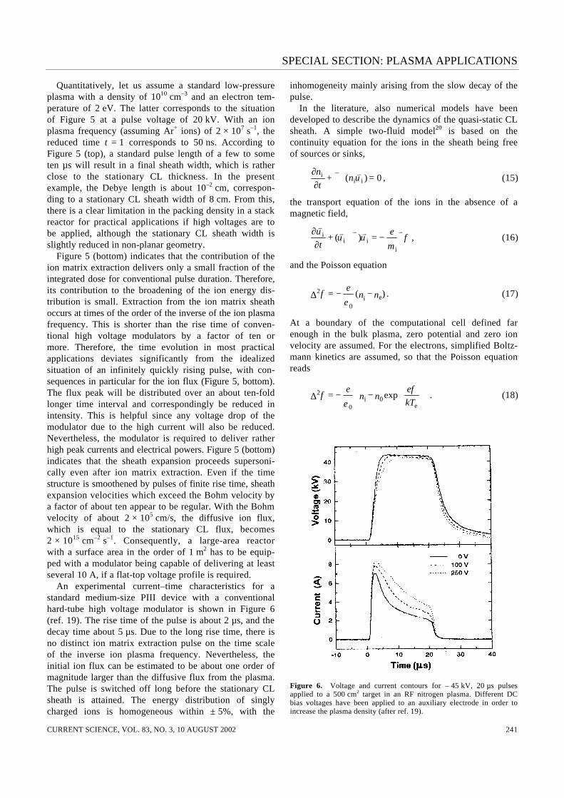
Quantitatively, let us assume a standard low-pressure plasma with a density of 1010 cm–3 and an electron tem-perature of 2 eV. The latter corresponds to the situation of Figure 5 at a pulse voltage of 20 kV. With an ion plasma frequency (assuming Ar+ ions) of 2 × 10⁷ s–1, the reduced time τ = 1 corresponds to 50 ns. According to Figure 5 (top), a standard pulse length of a few to some ten µs will result in a final sheath width, which is rather close to the stationary CL thickness. In the present example, the Debye length is about 10–2 cm, correspon-ding to a stationary CL sheath width of 8 cm. From this, there is a clear limitation in the packing density in a stack reactor for practical applications if high voltages are to be applied, although the stationary CL sheath width is slightly reduced in non-planar geometry. Figure 5 (bottom) indicates that the contribution of the ion matrix extraction delivers only a small fraction of the integrated dose for conventional pulse duration. Therefore, its contribution to the broadening of the ion energy dis-tribution is small. Extraction from the ion matrix sheath occurs at times of the order of the inverse of the ion plasma frequency. This is shorter than the rise time of conven-tional high voltage modulators by a factor of ten or more. Therefore, the time evolution in most practical applications deviates significantly from the idealized situation of an infinitely quickly rising pulse, with con-sequences in particular for the ion flux (Figure 5, bottom). The flux peak will be distributed over an about ten-fold longer time interval and correspondingly be reduced in intensity. This is helpful since any voltage drop of the modulator due to the high current will also be reduced. Nevertheless, the modulator is required to deliver rather high peak currents and electrical powers. Figure 5 (bottom) indicates that the sheath expansion proceeds supersoni-cally even after ion matrix extraction. Even if the time structure is smoothened by pulses of finite rise time, sheath expansion velocities which exceed the Bohm velocity by a factor of about ten appear to be regular. With the Bohm velocity of about 2 × 105 cm/s, the diffusive ion flux, which is equal to the stationary CL flux, becomes 2 × 1015 cm–2 s–1. Consequently, a large-area reactor with a surface area in the order of 1 m2 has to be equip-ped with a modulator being capable of delivering at least several 10 A, if a flat-top voltage profile is required. An experimental current–time characteristics for a standard medium-size PIII device with a conventional hard-tube high voltage modulator is shown in Figure 6 (ref. 19). The rise time of the pulse is about 2 µs, and the decay time about 5 µs. Due to the long rise time, there is no distinct ion matrix extraction pulse on the time scale of the inverse ion plasma frequency. Nevertheless, the initial ion flux can be estimated to be about one order of magnitude larger than the diffusive flux from the plasma. The pulse is switched off long before the stationary CL sheath is attained. The energy distribution of singly charged ions is homogeneous within ± 5%, with the
inhomogeneity mainly arising from the slow decay of the pulse. In the literature, also numerical models have been developed to describe the dynamics of the quasi-static CL sheath. A simple two-fluid model20 is based on the continuity equation for the ions in the sheath being free of sources or sinks,
,0)( iii = n +
t
nυvv
⋅∇∂
∂ (15)
the transport equation of the ions in the absence of a magnetic field,
,)(i
iii
m
e = +
tφυυ
υ∇−∇⋅
∂∂ vvvv
v
(16)
and the Poisson equation
.)( ei0
2 nn e
= −−∆ε
φ (17)
At a boundary of the computational cell defined far enough in the bulk plasma, zero potential and zero ion velocity are assumed. For the electrons, simplified Boltz-mann kinetics are assumed, so that the Poisson equation reads
.expe
0i0
2 kT
enn
e =
−−∆
φ
εφ (18)
Figure 6. Voltage and current contours for – 45 kV, 20 µs pulses applied to a 500 cm2 target in an RF nitrogen plasma. Different DC bias voltages have been applied to an auxiliary electrode in order to increase the plasma density (after ref. 19).

SPECIAL SECTION: PLASMA APPLICATIONS
CURRENT SCIENCE, VOL. 83, NO. 3, 10 AUGUST 2002 242
Equations 15, 16 and 18 are solved numerically for a given pulse shape, starting from V = 0 and determining the locally resolved densities and the potential for each time step. An example is given in Figure 7 (ref. 21), which shows the sheath edge velocity as function of the sheath width formed during the first 5 µs of a 5 kV pulse applied to the substrate. The model result is compared to experimental data from laser-induced fluorescence (LIF) and from a Langmuir probe. Reasonable agreement is found. The initial sheath velocity during the rise of the pulse exceeds the Bohm velocity by more than a factor of ten. The models discussed above allow a rather precise prediction of PBII ion fluxes and, consequently, ion doses per pulse. This becomes particularly important for 3D substrates, with a resulting dose distribution which is in general non-uniform along the surface. This issue will be qualitatively addressed in the following. For a 2D treatment, the above analytical model can be extended in an approximate way22,23, assuming a constant charge density within the sheath and neglecting the diffusive ion flux, which is justified for sufficiently short pulses as shown above. For a realistic situation with a cylindrical item mounted on a holder, a snapshot of the resulting potential distribution is shown in Figure 8 for PIII in nitrogen at a pulse voltage of 30 kV. The ion trajectories are indicated as obtained from a numerical solution. The total ion dose arriving locally at the sub-strate surface per pulse is obtained by integration over time. The resulting local dose is shown in Figure 8 as an analogue contour along the surface of the cylindrical pin. It is seen that the implantation is laterally non-uniform with a substantial decrease towards the holder. At the top of the pin, the non-monotonous decrease towards the holder indicates that the ions do not strictly follow the
electric field lines, as they become very fast close to the surface of the substrate. Nevertheless, the observed non-uniformity would be expected to be tolerable for mechanical applications or even desired as, for example, in the case of drills. It should also be noted that the predictions of the simple model are in surprisingly good quantitative agreement with local dose measurements along the surface22,23. An important problem is also the PBII treatment of hollow structures such as trenches or bores, which has been treated both using the simple analytical/numerical model22 and the two-fluid model24, as discussed above. Recently, a more extended numerical model has been described25, which employs a time-dependent particle-in-cell (PIC) simulation26 of the plasma. Figure 9 is a schematic of dynamic sheath formation around a hollow structure. Initially, the plasma fills the trench provided its dimensions are large compared to the Debye length. (Thus, a conventional low-pressure plasma will not fill microelectronic structures with micrometre or even sub-micrometre dimensions.) Depending on the dimensions of the structure (now in the mm or cm range) and on the width of the expanding sheath, the plasma will be expelled from the hole. During this phase, all faces (bottom and side walls) will be implanted. When the sheath width becomes comparable to or larger than the hole dimensions, the plasma detaches as depicted in the bottom of Figure 9. In this situation, any significant ion incorporation at the side walls cannot be expected, since the ions are emitted normally to the sheath edge and follow approximately straight trajectories in a non-collisional sheath. Therefore, for a collisionless sheath which is necessary to deliver essentially full-energy ions, a nearly uniform trench or bore implantation can only be obtained for very short pulse significantly below 1 µs, provided the dimensions are still large compared to the Debye length. For very short pulses, however, the energy distribution may be broadened to due to the matrix sheath effect as
Figure 7. Sheath velocity as function of sheath width, as observed during the first 5 µs of a PIII pulse with a flat-top voltage of 5 kV in a nitrogen plasma. vB denotes the Bohm velocity (after ref. 21).
Figure 8. 2 D PIII into a cylindrical item mounted on a cylindrical holder. Equipotential lines and ion trajectories are shown. The contour along the surface indicates the dose distribution along the surface.

SPECIAL SECTION: PLASMA APPLICATIONS
CURRENT SCIENCE, VOL. 83, NO. 3, 10 AUGUST 2002 243
discussed above. In addition, new economical and technical difficulties arise, such as excessive cost of the high-voltage modulator and electrical interference. Another way to increase the uniformity of the 3D treat-ment, in particular of hollow structures, is to compromise it against the energy spectrum of the ions, which will be addressed below. A further important issue of practical relevance is the inner treatment of long tubes. Similar to trenches and bores, the plasma inside a tube can only be sustained if the inner diameter is large compared to the maximum sheath width. In addition, the plasma potential inside a long tube may follow the substrate voltage applied to the tube. As a remedy, it has been proposed to mount a coaxial inner electrode at ground potential which fixes the plasma potential and improves the uniformity of the treatment along the inner surface. Corresponding fluid model calculations are available27. For completion of the discussion of 3D PBII, the colli-sional sheath shall be briefly addressed in a qualitative way. At sufficiently high pressure, where the mean free path of the ions in the sheath becomes comparable to or smaller than the sheath width, scattering processes occur during the passage of the ions through the sheath. These may influence the energy distribution of the ions signi-ficantly, as well as their angular distribution at the sub-strate surface. At sheath widths in the order of 1 cm, collisions become significant at pressures of the order of 10–2 mbar and below, if only kinetic collisions in the gas
are taken into account. Main processes are the symmetric charge exchange between ions and neutrals, and the multiple scattering of ions at neutrals. Depending on the pressure, broad energy distribution results at the substrate, which increases monotonically towards low-energy, being associated by a full-energy peak towards lower pres-sure28. Simultaneously, the angular distribution of the ions at the substrate will be broadened, as shown schema-tically in Figure 10 (ref. 29). Thus, even when the plasma boundary is detached from the surface contour as indicated in Figure 9, significant side-wall implantation becomes feasible in a trench or hole, with the compro-mise of an energy distribution, which is broadened towards lower energy. Consequently, the implantation depth will be strongly reduced and smeared out. This is further enhanced by the oblique incidence with a broad angular distribution. Two remarks must be added in order to characterize the complexity of the problem. At increasing pressure, the sheath thickness will also decrease, counteracting the influence of scattering. Furthermore, the collision proce-sses will influence the sheath dynamics. Fluid-model calculations for a collisional sheath have been given in the literature30.
Ion–surface interaction
As discussed earlier, the plasma boundary physics deter-mines the characteristics of the ions impinging onto the surface of the substrate, such as flux and energy and angular distributions. With these boundary conditions at the solid surface, solid state phenomena determine the effects of ion implantation on the final properties of the modified surface and subsurface regions. Generally, the surface modification results from an extremely complica-ted interplay of physical and chemical effects, which act on widely different time scales. An individual ion is slowed down to energies in the order of the solid-state binding energies (some eV) within about 10–14 s. Asso-ciated collision cascades thermalize after about 10–12 s.
Figure 9. Schematic of dynamic sheath formation around a hollow structure.
Figure 10. Influence of scattering on angular distribution of ions impinging onto a flat target (left), and consequences for PBII into trenches (right) (after ref. 29).

SPECIAL SECTION: PLASMA APPLICATIONS
CURRENT SCIENCE, VOL. 83, NO. 3, 10 AUGUST 2002 244
During these phases, radiation defects are formed and partially annealed again. Subsequently, thermal diffusion of the implanted atoms and of the defects occurs at sufficiently high substrate temperature. The time con-stants of these diffusional processes may reach the typical durations of experiments or practical applications, i.e. 103 s. During all these processes, the stoichiometry and the structure of the subsurface region may be altered. Different kinds of chemical reaction may occur, such as the formation of new phases4, which may be homo-geneous or form precipitates. In particular, during the initial collisional phase and the thermalization of the cascade, an intimate mixing of the subsurface atoms occurs, which again may be enhanced or even hindered by hot chemistry. All these phenomena are influenced by the presence of radiation defects. For conventional II and PBII, the fluxes of ions are sufficiently low to exclude any interaction between the individual collision cascades, as far as the fast collisional phase (t < 10–12 s) is concerned. Therefore, for a dis-cussion of the basic phenomena, it is often sufficient to describe the phenomena associated with an individual incident ion. Figure 11 represents the trajectory of an individual ion with mass and atomic number m1 and Z1, respectively, and kinetic energy E0 incident on a solid with atoms of m2 and Z2. The interaction with the target atomic nuclei and the target electrons, being of statistical nature, results in significant scatter of the individual trajectories. Along each trajectory, an average energy loss per travelled distance s can be defined by the stopping power – dE/ds or the stopping cross-section
,d
d
x
E
n
1= S − (19)
where n denotes the atomic density of the target sub-stance. Assuming that the interactions of the ion with the atomic nuclei (so-called ‘nuclear’ or ‘elastic’ interaction) and the electrons (‘electronic’ or ‘inelastic’ interaction)
act independently, the total stopping cross-section is composed of a nuclear and an electronic fraction,
S = Sn + Se. (20)
Basically, the nuclear interaction is described by the elastic scattering of the ions at the target atoms in a screened Coulomb potential, resulting in simultaneous energy loss and angular scattering. A universal expre-ssion, i.e. being approximately valid for all combinations of ions and target atoms, has been developed by Lindhard and coworkers31 in terms of reduced quantities for the ion energy,
,)( 21
221
20 E mmeZZ
am4 =
+πε
ε (21)
and for the pathlength,
.)(
42
21
212 smm
mmna =
+πρ (22)
The reduced nuclear stopping cross-section is then obtained in a good approximation32 by
.)70818826(6.351
2.718)log(3.44
d
d
n
..++
+ =
−
−
εεε
εερε
(23)
Due to the small electron mass, angular deflections by electronic collisions are negligible. At ion velocities υi which are small compared to the electron velocity υ0 = αc of the first Bohr orbit, where α denotes the fine structure constant and c the velocity of the light, the electronic energy loss results from scattering at the target electrons, which can be approximated by a free electron gas. In this regime, electronic stopping is proportional to the ion velocity. Again, a universal formula has been given by Lindhard and Scharff33 according to
,)(
2
00
0 i2/332
232
1
267
12
e Z+Z
ZZae = S
//
/<
υ
υ
ε (24)
with a0 denoting the radius of the first Bohr orbit. At ion velocities being large compared to υ0, the ion is decele-rated by electronic excitation and ionization of the target atoms. Quantum-mechanical calculations in the first-order Born approximation yield the Bethe–Bloch formula34
,4
log1
)4(
2
1
1 e
e2
0
42
21
e Im
Em E
m
m
ðeZðZ
= S>
ε (25)
with the electron mass me and the mean ionization poten-tial I, which can be approximated by I = 10⋅Z2 eV. The intermediate range is difficult to describe. Therefore, an interpolation formula combining eqs (24) and (25) has been proposed according to
.111
eee
S
+ S
= S ><
(26) Figure 11. Schematic of an ion trajectory and its associated collision cascade.

SPECIAL SECTION: PLASMA APPLICATIONS
CURRENT SCIENCE, VOL. 83, NO. 3, 10 AUGUST 2002 245
This forms the base of semi-empirical tables which list the electronic stopping data over a wide range of ion energies and for many ion–target combinations35–38. Rather precise stopping data for all elemental combinations are also available from the computer program package SRIM (Stopping and Ranges of Ions in Matter) which can be downloaded through the internet39. The stopping cross-section for the case of nitrogen ions incident on iron is shown in Figure 12. The high-velocity regime of electronic stopping (eq. (25)) is not relevant for typical PBII energies, except for very light ions. At energies below about 10 keV, the nuclear stopping dominates. It becomes small compared to the electronic stopping at energies exceeding 100 keV. From the total stopping cross-section (eq. (24)), the mean total pathlength of the ion trajectories is obtained according to
.)(
d1 0
0t ES
E
n = R
E
∫ (27)
For ion implantation, however, the mean projected range Rp (see Figure 11) is of interest, which may be con-siderably smaller than the mean total pathlength due to multiple scattering. Only at high energies when substan-tial scattering occurs towards the very end of the trajec-tory where the nuclear scattering cross-sections become important, or in the case of heavy ions, m1 >> m2, where angular deflections become small kinematically, eq. (27) is a reasonable estimate of the implantation depth. Other-wise, the mean projected range can be obtained from transport calculations40,41. Results from transport calcula-tions using precise stopping powers can also be obtained from the SRIM package39.
The projected range of nitrogen incident on iron is shown in Figure 12 (bottom). For many ion–target com-binations, a reasonable estimate of the mean projected range as function of the ion energy is
.0p
keV
E
nm
R≈ (28)
For ions incident at an angle α with respect to the surface normal, the mean projected range scales geometrically if α is not too close to π/2, i.e.
.cos)0()( pp R = R ααα = (29)
It is further worthwhile to address the case of molecular ions, which are often present in PBII. When entering the surface, the energetic molecule quickly splits into its atomic constituents, with the kinetic energy being distri-buted proportionally to their masses. Thus, a diatomic molecular ion of only one element, such as N2
+ , can be regarded as two incident atoms with half the energy. Consequently, the mean projected range becomes
.2
,),( p2p
+ E
XR = EXR + (30)
For more detailed calculations of ranges and range distri-butions, computer simulations of the binary-collision approximation (BCA) type are available42, such as the well-known TRIM code43,44, which is also available in the SRIM computer package39. A trajectory plot of a TRIM simulation is given in Figure 13 for nitrogen implanted into iron. A large scatter of the individual ion trajectories is evident. The straggling of the mean projec-ted range is substantial (standard deviation 11.5 nm at a mean projected range of 23.4). It is further shown that, in addition to the primary ions, TRIM traces the full collisional cascades. Figure 14 shows the ion range dis-tribution together with the deposited energy distributions, as obtained from the simulation. As both electronic and nuclear stopping power decrease at decreasing energy, the deposited energy distributions are always shallower than the range distributions. Only a small fraction of the total electronic energy loss is due to the recoil atoms. In the collision cascades, the target substance is subject to radiation damage at sufficiently high ion energy. Target atoms may be knocked off their lattice sites by nuclear collisions. Some of these atoms may receive suf-ficient recoil energy to be transported sufficiently far away from their original site. After the thermalization of the cascade, Frenkel pairs remain consisting of an inter-stitial atom and a vacancy at the original site, which represent the simplest configuration of a radiation defect45. For Frenkel-pair formation, a minimum threshold energy of the recoil, the displacement threshold Ud, is required, being in the order of some 10 eV depending on the mate-rial. In the regime of the so-called ‘linear’ cascade, which is
Figure 12. Stopping and ranges of nitrogen ions in iron. (Top) Nuclear stopping according to eq. (23) (dotted line), electronic stopping from SRIM package39 with low-energy extrapolation Se ~ υi
(see eq. (24)) (dashed-dotted line) and total stopping (solid line). (Bottom) Mean projected range from SRIM package39 with low-energy extrapolation31.

SPECIAL SECTION: PLASMA APPLICATIONS
CURRENT SCIENCE, VOL. 83, NO. 3, 10 AUGUST 2002 246
valid for all applications of PBII, except for very heavy ions at very high energy (above about 100 keV), the number of Frenkel defects per incident ion can roughly be estimated using the Kinchin–Pease formula46
U
E= E .
2)(
d
00Fν (31)
The evaluation of eq. (31) shows that the number of generated defects exceeds the number of implanted ions by far at keV and higher energies. The depth distribution of generated Frenkel pairs follows closely the nuclear damage distribution. It should be noted that only the collisional damage has been addressed which remains after the thermalization of a collision cascade associated with a single ion track. Under real conditions involving elevated temperatures and high doses, point defects will migrate, saturate, anni-hilate and form extended defects, all depending on the specific material. Any details of these phenomena cannot be discussed here. As already indicated in Figure 11, target atoms can be sputtered47 from the surface provided the collision cas-cade penetrates the surface and contains atoms of suffi-ciently high energy to overcome the surface binding energy, Us. The surface binding energy is conventionally set equal to the enthalpy of sublimation, with values between about 2 eV and 8 eV for different materials. For the regime of linear cascades, Sigmund48 has derived a
Figure 13. TRIM95 trajectory plots for 100 nitrogen ions incident on iron at an energy of 20 keV. The point of incidence is indicated by the arrows. a, Side view of primary ion trajectories only; b–d, Including collision cascades: b, c, Side and top views respectively; d, View along the direction of incidence.
a
b c
d
Figure 14. Ion range and energy deposition distributions for nitrogen incident on iron at 20 keV, from a TRIM95 computer simulation with 1000 incident ions. The range distribution is normalized to 1, energy deposition distributions are normalized to the energy of incidence.

SPECIAL SECTION: PLASMA APPLICATIONS
CURRENT SCIENCE, VOL. 83, NO. 3, 10 AUGUST 2002 247
simple expression for the sputtering yield Ys, which denotes the number of sputtered atoms per incident ions:
.)(cm102.4)( 01
2
s
214
0s ES m
mæ
U = EY n
⋅ (32)
ζ = 0.2 . . . 0.6 is tabulated as a function of the mass ratio. The energy dependence of the sputtering yield is given by the energy dependence of nuclear stopping, Sn(E0). Equation (32) overestimates sputtering at very low energies, in particular for light ions, as the threshold energy is not taken into account correctly. A corres-ponding semi-empirical correction has been introduced by Bohdansky49. Figure 15 displays the sputtering yield for nitrogen incident on iron. At energies being characteristic for PBII, the sputtering yield varies only weakly with energy. It should be noted that surface contaminants such as oxides might reduce the sputtering yield by up to a factor of two due to an increased surface binding energy. Also BCA computer simulations can be reliably used for the prediction of sputtering yields. Data from TRIM (SRIM package39) are included in Figure 15. At typical PBII energies, sputtering yields are in the order of unity or even larger. Therefore, for high-dose ion implantation the influence of sputtering on the ion implantation has to be taken into account, since the sur-face is continuously eroded. A schematic is shown in Figure 16. At low incident fluence, ions are implanted according to their range distribution (see Figure 14). With increasing fluence, the surface erosion penetrates into the previously implanted zone. Finally, when the surface recession exceeds the mean projected range of the ions and the sputter yield is larger than one, a stationary profile is established with a balance of surface erosion and additional implantation. Under the simplifying assumption that the sputter yield does not change due to
the presence of the implanted atoms, the final stationary surface concentration of the implant results as
.)0(s
i Y
nxn == (33)
The development of sputter-controlled implantation pro-files represents an example of dynamic alteration of the target substance during ion processing. A more compli-cated example is the balance of deposition and sputter erosion during PIIAD. So-called ‘dynamic’ computer simulations of the BCA type can address such pheno-mena, the analytical treatment of which is difficult. Figure 17 shows the result of an ion-beam-assisted depo-sition (IBAD) process obtained with the TRIDYN code50. (A present version51 of TRIDYN is capable of treating a multi-component and inhomogeneous target material being subject to energetic or thermal fluxes of up to five different species.) Neutral titanium atoms at thermal energies are evaporated onto an iron substrate under simultaneous bombardment with 1 keV nitrogen ions, both beams being incident at an angle of 20° with respect to the surface normal. At a sufficiently low ion-to-neutral flux (I/A) ratio of 1 : 1 (Figure 17, bottom), a titanium nitride film is built up. (It should be noted that the program takes into account the stoichiometric saturation of the nitrogen concentration.) At a higher I/A ratio of 3 : 1 (Figure 17, top), only a non-stoichiometric mixed surface layer is obtained without a continuously growing film, as re-sputtering becomes dominant. This is confirmed by the retention curves of Figure 18, with a saturation of the implanted amounts at the higher I/A ratio already at low fluence. More detailed information can be extracted. Even for the lower I/A ratio, the com-parison of the sum of the retained amounts with the total incident fluence (Figure 18) shows that re-sputtering is significant. Also at equal fluences of nitrogen and tita-nium, the retained amount of nitrogen is higher due to the energetic implantation, which yields nitrogen excess
Figure 15. Sputtering yield for nitrogen ions incident on iron according to the Sigmund’s48 formula (eq. (32)) (solid line), modified by the threshold correction according to Bohdansky49 (dotted line), and from TRIM computer simulation (points from the SRIM package39, version 2000.39).
Figure 16. Schematic of the implant concentration profile, ni(x), under sputter control with a surface recession velocity υs.

SPECIAL SECTION: PLASMA APPLICATIONS
CURRENT SCIENCE, VOL. 83, NO. 3, 10 AUGUST 2002 248
(compared to titanium) at the film/substrate interface (see Figure 17, bottom). A strong mixing between the film and the substrate is found even for the lower I/A ratio, which will increase the adhesion of the film. It should be noted that these IBAD results cannot be directly transferred to the PIIAD process due its low duty cycle of the energetic bombardment. Nevertheless, they provide valuable information on the different mechanisms.
Applications
At present, PBII techniques have not yet been established in broad fields of industrial production, although several applications appear to be very promising, as it will be shown below. For the transfer from scientific research and laboratory development to industrial application, the feasibility is critically determined by further aspects such as safety, duty time of the device, up-scaling and the possibility of large-area processing, and in particular, the processing costs. PBII has to compete with a number of techniques, which are well established and have been developed through many years, such as plasma nitrid- ing for tribological purposes or conventional ion implantation in microelectronics. Therefore, it has to be clearly demonstrated that PBII allows to realize new and improved surface properties at no or tolerable increase of the production cost. In this concluding chapter, a few
examples will be addressed, without, however, stressing on the economical aspects.
Microelectronics
The technical development in microelectronics (roadmap) is determined by a continuously increasing miniaturi-zation at a simultaneously increasing wafer diameter. With shrinking lateral dimensions, the dimensions in the normal direction also have to shrink. For the indispen-sable fabrication steps using ion implantation, the ion energies are to be reduced correspondingly. The transport of low-energy ions or the slowing down of high-energy ions represents a serious problem for the implanter technology, in particular, if large areas are required. Both requirements mentioned above can be met by PBII, so that this technique has entered the research laboratories of large producers of ion implantation equipment for microelectronics52. The main application of ion implantation in the elec-tronics industry is the doping of semiconductors. The formation of ultra-shallow p+/n junctions by PIII has been successfully demonstrated29. A two-step process is employed: For pre-amorphization, in order to avoid channelling during the doping implant, SiFx
+ ions from an SF4 plasma are implanted into the crystalline silicon. Subsequently, BFx
+ ions from a BFs plasma deliver the boron dopant. During subsequent annealing at tempe-ratures exceeding 1000°C, the doped surface layer is recrystallized and the fluorine removed. Junction depths down to 40 nm have been achieved. High-speed dynamic random-access memories (DRAMs) with a high packing density require large-area trench capa-citors which can be realized by shallow, high-doping of the trench walls. Figure 19 shows a cross-sectional TEM micrograph obtained after PIII trench-doping. A surpri-singly high uniformity of the doping depth is observed53, which is ascribed to the scattering of ions in the plasma sheath. A higher substrate voltage (10 kV) reduces the
Figure 17. TRIDYN simulation of IBAD for TiN thin-film depo-sition. Ti atoms arrive at the Fe surface at thermal energies under simultaneous bombardment with 1 keV nitrogen ions. Elemental con-centration profiles as function of depth after a total (N++Ti) fluence of 3⋅1017 atoms/cm2 are also shown. (Top) Ion-to-neutral ratio of 3 : 1. (Bottom) Ion-to-neutral ratio of 1 : 1. For details, see text.
Figure 18. IBAD simulated by TRIDYN (see Figure 17): Retained fluence for two different ion-to-neutral arrival ratios. At higher nitro-gen-ion-to-titanium ratio, resputtering is dominant. Therefore, theretained fluence saturates.

SPECIAL SECTION: PLASMA APPLICATIONS
CURRENT SCIENCE, VOL. 83, NO. 3, 10 AUGUST 2002 249
side-wall doping depth with respect to the bottom, as the ion scattering is reduced at larger energies. Trenches with aspect ratios up to 12 at a trench width of 1 µm have been successfully treated in this way. With decreasing feature size, it becomes also necessary to screen the near-surface layer of the wafer, which carries the microelectronic structures, against the under-lying bulk, both in order to avoid electrical field pene-tration and to block diffusing impurities. For this purpose, buried SiO2 layers can be employed. These are conven-tionally produced by high-dose ion implantation of oxygen into the silicon wafer and subsequent thermal annealing (the so-called SIMOX structure: Separation by IMplanted OXygen). Figure 20 shows the oxygen depth profile obtained from PIII in an oxygen plasma at a target voltage of 50 kV. The individual contributions of the main fraction of molecular ions with an energy of 25 keV/atom, and the small fraction of atomic ions with 50 keV energy can clearly be identified. This represents an unwanted profile-broadening for the purpose of SIMOX formation. Nevertheless, a well-established buried layer with sharp and smooth interfaces is obtained after annealing54.
In SIMOX structures, the quality of the top crystalline silicon layer is reduced due to irradiation defects, which remain even during the annealing at very high tempe-rature. In order to overcome this problem, an alternative process has been proposed, which is called ‘smart cut’. A schematic representation of the process sequence is shown in Figure 21. The silicon wafer is first oxidized thermally. It is then bombarded by light ions (hydrogen or helium), which cause little damage. At a sufficiently high dose, gas-filled cavities form in a shallow band close to the mean projected range of the ions. The structure is then attached with its oxidized surface to another wafer using the conventional technique of anodic-bonding. With a proper thermal treatment, the bonded two-wafer structure then cracks along the plane contain-ing the bubbles. A final surface-lapping finishes the process. It has been demonstrated55 that buried oxide layers of a thickness of about 30 nm can be formed under a crystalline silicon layer of about the same thickness, when the ‘smart cut’ is induced by PIII using 35 keV helium ions. In a recent experiment, the modification of oxidation behaviour of nitrogen and argon-implanted Si wafers is reported56. Nitrogen and argon ions are implanted in Si at various energies at different implantation doses. Post-implantation, wet-oxidation results show that argon-implanted Si has higher oxide layer thickness with increase in the implanted ion dose (see Figure 22). The results can be used to control the gate oxide layer thickness for memory and logic transistors. The growth of carbide, nitride and oxide of silicon either simultaneously or as multilayers is also gaining increasing importance. This combines the SiC semiconductor, which is widely used in high temperature, high frequency and high power electronics, with the insulators Si3N4 and SiO2, which are also necessary for semiconductor design. Volz and Ensinger57 describe the growth of SiC thin films by introducing methane PIII into Si at 850°C, which are subsequently annealed at 1250°C for 5 h. As-implanted, amorphous regions are observed surrounding
Figure 19. Conformal trench-doping using PIII from a BF3 plasma at 6.5–10–3 mbar and 5 kV target voltage, for two different aspect ratios of 5 (left) and 1 (right). The depth of the trenches is about 5 µm (after ref. 53).
Figure 20. SIMOX formation by PIII from an oxygen plasma: As-implanted oxygen profile after annealing at 1270°C for 2 h. The sub-strate voltage was 50 kV, implanted dose 3⋅1017 O/cm2 (after ref. 54).
Figure 21. ‘Smart cut’ technique to form buried oxide layers.

SPECIAL SECTION: PLASMA APPLICATIONS
CURRENT SCIENCE, VOL. 83, NO. 3, 10 AUGUST 2002 250
small heteroepitaxial grains of SiC. After annealing, the SiC is completely cubic and heteroepitaxial with a 5 : 4 coincidence lattice at the interface, which minimizes stress due to the 20% lattice misfit between Si and c-SiC. SiO2 is grown by oxidation and stays amorphous even after high-temperature annealing. The final structure is shown in Figure 23.
Tribology
Surface treatment, with the aim to reduce friction and wear, is indispensable for many machine components, tools, and also medical purposes, e.g. for artificial joints. Beyond the broad applications in electronics, this is the main field of the application of ion implantation in indus-trial production. The high potential of ion implantation in tribology has been recognized since a longtime58,59. Nevertheless, cost problems have impeded a major and broad breakthrough, although ion implantation is routinely applied to the hardening of surgical prostheses60. Therefore, with its prospective for cost reduction, PBII is a promising new technique, in particular in this field. However, as the maximum ion energy in PBII is limited with respect to conventional implantation, its main advantage is the ability to deliver large doses for the formation of deep, modified layers in connection with diffusion. Diffusive processes using nitrogen are broadly applied to the surface-hardening of metallic components, in parti-cular steel. A number of different techniques are conventionally applied in industrial production, such as salt-bath nitriding, nitriding from the gas phase, and plasma-nitriding. Plasma-nitriding exhibits characteristic advantages, being environmentally clean, and allowing an efficient low-temperature processing due to the acti-vation in the plasma. For a large variety of different tool and machine components, a longstanding experience with
plasma-nitriding has been acquired in mostly small companies, with successful applications mostly for con-ventional tool steel. In this area of standard materials, it will be difficult to compete using PIII. The investment and production costs of PIII are higher compared to plasma-nitriding, as the considerably lower working pres-sure requires a secondary vacuum pump, a costly high-voltage modulator has to be provided, and a reduced packing density results from the sheath expansion. Physically, the main advantage of PIII is the availa-bility of higher ion energies, with a number of potential beneficial consequences for practical application. As an example, nitrogen ions can be implanted behind a diffusion barrier, which is formed by a surface oxide. Thereby, the efficiency of the nitriding process can be significantly improved with higher nitrogen incorpora-tions achieved within shorter times. In materials for which only a certain maximum temperature is allowed, e.g. in order to avoid the formation of undesired phases, PIII-nitriding might therefore be advantageous, as the processing times can be held within tolerable limits even at large depths of nitriding. The nitriding of austenitic stainless steel is of parti-cular interest61,62. Its chemical inertness enables applica-tions in widely different fields. However, it exhibit poor mechanical surface properties such as low hardness and a high wear rate. With conventional nitriding, specific problems have been encountered. In order to avoid a transformation of the chromium oxide into chromium nitride at the surface, by which the anticorrosive pro-perties would be lost, the temperature of the process is limited, thus requiring very long processing times. Although the detailed mechanisms have not yet been investigated, one might anticipate that surface nitride formation can be avoided by PIII due to the relatively large depth of implantation. In addition, the process is accelerated due to the efficient incorporation of nitrogen behind the oxide barrier. Results from several groups63–65 confirm the high potential of PIII for the nitriding of stainless steel. Figure 24 shows concentration–depth profiles obtained after
Figure 22. Oxide layer thickness versus PIII ion dose for nitrogen and argon-implanted Si wafers at 10 keV (after ref. 56).
Figure 23. TEM cross-section of a SiC/Si/SiO2 sandwich structure on Si obtained by methane PIII at 850°C and subsequent annealing at 1250°C. a, Bright field; b, Dark-field Si, and c, Dark-field SiC (after ref. 57).
a b c

SPECIAL SECTION: PLASMA APPLICATIONS
CURRENT SCIENCE, VOL. 83, NO. 3, 10 AUGUST 2002 251
Figure 26. DLC coatings produced in a PBII set-up for large-area embossing of decorative material. Pulsed DC bias at – 4 kV, a pulse duration of 20 µs, and a repetition rate of 2 kHz are employed at 20 µbar pressure of acetylene.
PIII-nitriding, with a nitriding depth of about 40 µm. The processing time was about 5 h. The nitrogen profile shows a diffusion-like fraction with the source just below the surface, which, however, appears to be superimposed to a profile of nearly rectangular shape extending to the full depth. This can be explained by diffusion under the influence of traps66,67. Nitrogen atoms get trapped at the chromium alloy atoms with a corresponding maximum atomic concentration of about 20%. Thereby, the so-called ‘expanded austenite’ is formed68, which has been identified by X-ray diffraction to maintain the austenite structure with a lattice expansion of about 7%. By diffusion through this layer, nitrogen is continuously added to the interface with the underlying bulk, thus extending the thickness of the nitrided layer. No or merely a small fraction of chromium nitride can be detected at sufficiently low temperature. The nitrided
surface fulfils well the practical requirements. The surface hardness is increased by a factor of 2–3. Compared to the untreated surfaces, the wear rates are drastically reduced, by about three orders of magnitude in case of stainless steel. Simultaneously, the corrosion behaviour is not deteriorated or is even slightly improved. Recently, PIII experiments for the incorporation of nitrogen in material surfaces are also performed at lower substrate bias (~ 1 kV), at high repetition rates of pulse voltages69,70. For many applications, the resulting ion energy is sufficient to penetrate the material surface, so that the nitrogen diffuses inside owing to elevated sub-strate temperature71. A wide variety of materials are reported to be treated in this way. An example is given in Figure 25. Processing at lower substrate bias is advan-tageous because of reduced sheath thickness and the lower secondary electron emission yield. In addition, the high-voltage pulse equipment is considerably cheaper. Recently, PBII of methane has been applied to produce hard hydrogenated carbon (DLC) coatings on large-area plates for embossing of decorative material72. Figure 26 shows the plates which later will be spanned onto embossing drums, arranged in a large-volume PBII reactor of about 2 m length. Pulsed DC at a few kV is employed simultaneously for plasma production and ion implantation. Thus, the production cost is kept low. By the treatment, lifetime of the plates is improved by a factor of 4–5 compared to the uncoated material. The DLC coating also avoids adhesive wear, which would degrade the pattern.
Biomaterial development
One of the major developments that has taken place recently is improving the biocompatibility of materials using PBII alone or along with other PVD or CVD
Figure 24. Elemental depth profiles obtained from GDOS (glow discharge optical emission spectroscopy), after PIII treatment of stainless steel in a nitrogen plasma. Note that the absolute concen-trations are subject to large errors, in particular for the light elements.
Figure 25. Microhardness as a function of depth in AISI 52100 steel after PIII-nitriding at a substrate pulsed bias of – 1 kV and temperature of 500°C, for various treatment durations. It is seen that with increas-ing time, nitrogen diffuses to larger depths.

SPECIAL SECTION: PLASMA APPLICATIONS
CURRENT SCIENCE, VOL. 83, NO. 3, 10 AUGUST 2002 252
processes. Examples are given in Figures 27 and 28 for materials which can be used for artificial heart valves. Whereas the standard low-temperature isotropic pyrolytic (LTI) carbon exhibits a strong aggregation of a thrombus after in vivo exposure in a dog’s heart, no significant thrombus is observed under identical conditions on a
titanium-based biomaterial which has been treated using oxygen PIII73 (Figure 27). The bombardment with oxygen ions is used to control the growth of the oxide phases, so as to form the rutile phase. Also the biocompatibility of LTI carbon materials profits signi-ficantly from PIII74. Due to nitrogen implantation, the platelet density after blood exposure is strongly reduced (Figure 28). This is probably due to the formation of a CNx surface layer. So far, these promising results have not been transferred to routine surgery, which is due to a number of impeding factors, such as the lengthy test procedures which are required legally before new arti-ficial materials can be introduced into a human body.
1. Williams, J. S. and Poate, J. M. (eds) Ion Implantation and Ion Beam Processing, Academic Press, New York, 1984.
2. Rimini, E., Ion Implantation: Basics to Device Fabrication, Kluwer Academic Publishers, Boston, 1995.
3. Nastasi, M., Hirvonen, J. K. and Mayer, J. W., Ion Beam Pro-cessing: Fundamentals and Applications, Cambridge University Press, Cambridge, 1996.
4. Nolfi, F. V. (ed.), Phase Transformation During Irradiation, Applied Science Publishers, London, 1983.
5. Smidt, F. A., Int. Mater. Rev., 1990, 35, 61. 6. Wolf, G. K. and Ensinger, W., Nucl. Instrum. Methods B, 1991,
59/60, 173. 7. Conrad, J. R., J. Appl. Phys., 1987, 62, 777. 8. Tendys, J., Donnelly, I. J., Kenny, M. J. and Pollock, J. T. A.,
Appl. Phys. Lett., 1988, 53, 2143. 9. Conrad, J. R. and Sridharan, K. (eds), J. Vac. Sci. Technol. B,
1994, 12, 813. 10. Collins, G. A. and Short, K. T. (eds), Surf. Coat. Technol., 1996,
85. 11. Möller, W., Günzel, R. and Wieser, E. (eds), ibid, 1997, 93. 12. Mantese, J. (ed.), J. Vac. Sci. Technol. B, 1999, 17. 13. Yamada, I., Yukimura, K. and Horino, Y. (eds), Surf. Coat. Tech-
nol., 2001, 136. 14. Anders, A., ibid, 1997, 93, 158. 15. Brückner, J., Günzel, R., Richter, E. and Möller, W., ibid, 1998,
103–104, 227. 16. Lieberman, M. A. and Lichtenberg, A. J., Principles of Plasma
Discharges and Materials Processing, John Wiley, New York, 1994.
17. Conrad, J. R., Radtke, J. L., Dodd, R. A., Worzala, F. J. and Tran, R. C., J. Appl. Phys., 1987, 62, 4591.
18. Riemann, K.-U. and Daube, Th., ibid, 1999, 86, 1202. 19. Collins, G. A., Short, K. T. and Tendys, J., Surf. Coat. Technol.,
1997, 93, 181. 20. Widner, M., Alexeff, I., Jones, W. D. and Lonngren, K. E., Phys.
Fluids, 1970, 13, 2532. 21. Goeckner, M. J., Malik, S. M., Conrad, J. R. and Breun, R. A.,
Phys. Plasmas, 1994, 1, 1064. 22. Mändl, S., Barradas, N. P., Brutscher, J., Günzel, R. and Möller,
W., Nucl. Instrum. Methods B, 1997, 127/128, 996. 23. Mändl, S., Reuther, H., Brutscher, J., Günzel, R. and Möller, W.,
1997, Surf. Coat. Technol. 93, 229. 24. Sheridan, T. E., J. Phys. D, 1995, 28, 1094. 25. Paulus, M., Rauschenbach, B., Stals, L. and Rüde, U., IEEE
Proceedings of the International Conference on Ion Implantation Technology, Kyoto, 1998, p. 1187.
26. Birdsall, C. K. and Langdon, A. B., Plasma Physics Via Computer Simulation, Institute of Physics Publishing, Bristol, 1991.
27. Zeng, X. C., Kwok, T. K., Liu, A. G., Chu, P. K., Tang, B. Y. and Sheridan, T. E., Appl. Phys. Lett., 1997, 71, 1035.
Figure 28. Reduction of platelet density by nitrogen PIII, on LTI carbon after blood exposure. PIII parameters are a substrate bias of 30 kV, a nitrogen ion dose of 3.7⋅1017/cm2 and a substrate temperature of 500°C.
Figure 27. Surface morphology of artificial heart valve material after implantation into a dog’s right atrium for 30 days. a, LTI carbon with-out additional surface treatment; b, Titanium alloy biomaterial with a PIIAD Ti–O coating.
b
a

SPECIAL SECTION: PLASMA APPLICATIONS
CURRENT SCIENCE, VOL. 83, NO. 3, 10 AUGUST 2002 253
28. Davis, W. D. and Vanderslice, T. A., Phys. Rev., 1963, 131, 219.
29. Jones, E. C., Linder, B. P. and Cheung, N. W., Jpn. J. Appl. Phys., 1996, 35, 1027.
30. Sheridan, T. E. and Goeckner, M. J., J. Appl. Phys., 1995, 77, 4967.
31. Lindhard, J., Nielsen, V. and Scharff, M., K. Dan. Vidensk. Selsk. Mat. Fys. Medd., 1968, 16, 10.
32. Matsunami, N., Yamamura, Y., Hikawa, Y., Itoh, N., Kazumata, Y., Miyagawa, S., Morita, K., Shimizu, R. and Tawara, H., 1983, Report IPPJ-AM-32, Institute of Plasma Physics, Nagoya University.
33. Lindhard, J. and Scharff, M., Phys. Rev., 1961, 124, 128. 34. Fano, U., Annu. Rev. Nucl. Sci., 1963, 13, 1. 35. Andersen, H. H. and Ziegler, J. F., The Stopping and Range of
Ions in Solids (ed. Ziegler, J. F.), Pergamon Press, New York, 1977, vol. 3.
36. Ziegler, J. F. (ed.), The Stopping and Range of Ions in Solids, Pergamon Press, New York, 1977, vol. 4.
37. Ziegler, J. F. (ed.), ibid, Pergamon Press, New York, 1980, vol. 5. 38. Littmark, U. and Ziegler, J. F., in The Stopping and Range of Ions
in Solids (ed. Ziegler, J. F.), Pergamon Press, New York, 1980, vol. 6.
39. Ziegler, J. F., ‘SRIM-2000’, Computer software package. Can be downloaded via internet http://www.SRIM.org.
40. Lindhard, J., Scharff, M. and Schiøtt, H., K. Dan. Vidensk. Selsk. Mat. Fys. Medd., 1963, 33, 14.
41. Schiøtt, H. E., ibid, 1966, 25, 9. 42. Eckstein, W., Computer Simulation of Ion–Solid Interactions,
Springer-Verlag, Berlin, 1991. 43. Ziegler, J. F., Biersack, J. P. and Littmark, U., in The Stopping
and Range of Ions in Solids (ed. Ziegler, J. F.), Pergamon Press, New York, 1985, vol. 1.
44. Biersack, J. P. and Haggmark, L. G., Nucl. Instrum. Methods, 1980, 174, 257.
45. Merkle, K. L., in Radiation Damage in Metals (eds Petersen, N. L. and Harkness, S. D.), American Society for Metals, Metals Park, Ohio, 1976.
46. Kinchin, G. H. and Pease, R. S., Rep. Prog. Phys., 1955, 18, 1. 47. Sigmund, P. in Sputtering by Particle Bombardment I (ed.
Behrisch, R.), Springer-Verlag, Berlin, 1981. 48. Sigmund, P., Phys. Rev., 1969, 184, 383. 49. Bohdansky, J., Nucl. Instrum. Methods, 1984, B2, 587. 50. Möller, W., Eckstein, W. and Biersack, J. P., Comp. Phys. Com-
mun., 1988, 51, 355. 51. Möller, W. and Posselt, M., TRIDYN_FZR User Manual, Forsch-
ungszentrum Rossendorf, Report FZR-317, 2001. 52. Felch, S. B., Bersuker, G., Larsen, L. A., Lee, B. S. and Shi, J.,
IEEE Proceedings of the International Conference on Ion Imp-lantation Technology, Kyoto, 1998, p. 403.
53. Yu, C. and Cheung, N. W., IEEE Elec. Dev. Lett., 1994, 15, 196.
54. Chu, P. K. in Materials Modification and Synthesis by Ion Beam Processing (eds Alexander, D. E., Cheung, N. W., Park, B. and Skorupa, W.), MRS Symposium Proceedings, Materials Research Society, Pittsburgh, 1997, vol. 438, p. 333.
55. Lu, X., Iyer, S. S. K., Min, J., Fan, Z., Liu, J. B., Chu, P. K., Hu, C. and Cheung, N. W., Proceeding IEEE International SOI Conference, 1996, p. 48.
56. Rajkumar, Kumar, M., George, P. J., Mukherjee, S. and Chari, K. S., Paper presented at PBII 2001, Grenoble; submitted to Surf. Coat. Technol.
57. Volz, K. and Ensinger, W., Paper presented at PBII 2001, Gre-noble; submitted to Surf. Coat. Technol.
58. Hirvonen, J. K., Mater. Sci. Eng. A, 1989, 116, 167. 59. Mikkelsen, N. J. and Straede, C. A., Surf. Coat. Technol., 1992,
51, 152. 60. Sioshansi, P. and Tobin, E. J., ibid, 1996, 83, 175. 61. Zhang, Z. L. and Bell, T., Surf. Eng., 1985, 1, 131. 62. Menthe, E., Rie, K.-T., Schultze, J. W. and Simson, S., Surf. Coat.
Technol., 1995,74/75, 175. 63. Collins, G. A., Hutchings, R., Short, K. T., Tendys, J., Li, X. and
Samandi, M., ibid, 1995, 74/75, 417. 64. Blawert, C., Knoop, F. M., Weisheit, A. and Mordike, B. L., ibid,
1996, 85, 15. 65. Mändl, S., Günzel, R., Richter, E. and Möller, W., ibid, 1998,
100/101, 367. 66. Möller, W., Parascandola, S., Kruse, O., Günzel, R. and Richter,
E., ibid, 1999, 116–119, 1. 67. Parascandola, S., Möller, W. and Williamson, D. L., Appl. Phys.
Lett., 2000, 75, 2194. 68. Samandi, M., Shedden, B. A., Smith, D. I., Collins, G. A., Hutch-
ings, R. and Tendys, J., Surf. Coat. Technol., 1993, 59, 261. 69. Mukherjee, S. and John., P. I., ibid, 1997, 93, 188. 70. Mukherjee, S., Chakraborty, J., Gupta, S. K., Raole, P. M., John.,
P. I., Rao, K. R. M. and Manna, I., Paper presented at PBII 2001, Grenoble and submitted to Surf. Coat. Technol.
71. Rao, K. R. M., Mukherjee, S., Raole, P. M. and Manna, I., accepted in Surf. Coat. Technol.
72. Wei, R., Arps, J. H. and Walter, K. C., Paper presented at PBII 2001, Grenoble and submitted to Surf. Coat. Technol.
73. Yang, P., Huang, N., Leng, Y. X., Chen, J. Y., Sun, H., Wang, J., Wang, J., Wu, X., Chen, F. and Chu, P. K., Paper presented at PBII 2001, Grenoble and submitted to Surf. Coat. Technol.
74. Mändl, S. and Rauschenbach, B., Paper presented at PBII 2001, Grenoble and submitted to Surf. Coat. Technol.
ACKNOWLEDGEMENT. S.M. is grateful to the Alexander von Humboldt foundation for financial support for his stay at Forsch-ungszentrum Rossendorf.