Embed Size (px)
Citation preview
General rights Copyright and moral rights for the publications made accessible in the public portal are retained by the authors and/or other copyright owners and it is a condition of accessing publications that users recognise and abide by the legal requirements associated with these rights.
• Users may download and print one copy of any publication from the public portal for the purpose of private study or research. • You may not further distribute the material or use it for any profit-making activity or commercial gain • You may freely distribute the URL identifying the publication in the public portal
If you believe that this document breaches copyright please contact us providing details, and we will remove access to the work immediately and investigate your claim.
Downloaded from orbit.dtu.dk on: Nov 12, 2018
Planar Integrated Magnetics (PIM) Module in Hybrid Bidirectional DC-DC Converter forFuel Cell Application
Ouyang, Ziwei; Zhang, Zhe; Thomsen, Ole Cornelius; Andersen, Michael A. E.
Published in:I E E E Transactions on Power Electronics
Link to article, DOI:10.1109/TPEL.2011.2129598
Publication date:2011
Link back to DTU Orbit
Citation (APA):Ouyang, Z., Zhang, Z., Thomsen, O. C., & Andersen, M. A. E. (2011). Planar Integrated Magnetics (PIM) Modulein Hybrid Bidirectional DC-DC Converter for Fuel Cell Application. I E E E Transactions on Power Electronics.DOI: 10.1109/TPEL.2011.2129598
Copyright (c) 2011 IEEE. Personal use is permitted. For any other purposes, Permission must be obtained from the IEEE by emailing [email protected].
This article has been accepted for publication in a future issue of this journal, but has not been fully edited. Content may change prior to final publication.
Planar Integrated Magnetics (PIM) Module in Hybrid
Bidirectional DC-DC Converter for Fuel Cell Application
Ziwei Ouyang, Student Member, IEEE, Zhe Zhang, Student Member, IEEE, Ole C. Thomsen, Member, IEEE,
and Michael A. E. Andersen, Member, IEEE,
Department of Electrical Engineering,
Technical University of Denmark,
Kgs. Lyngby, DK-2800, Denmark, [email protected]
ABSTRACT
In most power electronics converters, the overall volume is mainly determined by the number of parts and
the size of passive components. Integrated magnetics and planar magnetics techniques therefore have been an
excellent option in order to reduce the counts and the size of magnetic components, hereby increasing the power
density of converters. In this paper, a new planar integrated magnetics (PIM) module for a phase-shift plus duty
cycle controlled hybrid bi-directional dc-dc converter is proposed, which assembles one boost inductor and two
transformers into an E-I-E core geometry, reducing the number of parts, the total volume of converter, as well as
the total core loss of the magnetic components. AC losses in the windings and leakage inductance of the
transformers are kept low by interleaving the primary and secondary turns of the transformers. To verify the
validity of the design approach and theoretical analysis, a lab prototype employing the PIM module is
implemented for a fuel cell application with 20~40 V input voltage and 400 V output voltage. Detailed results
from the experimental comparisons demonstrate that the PIM module is fully functional and electromagnetically
equivalent to the discrete magnetics and a significant reduction of size can be achieved by using the PIM module.
Index Terms-- planar integrated magnetics, transformer, inductor, interleaving, hybrid, dc-dc converter
and fuel cell.
Manuscript submitted August 31, 2010, revised November 23, 2010, accepted March 1, 2011. This work is supported by Flux A/S. Parts of this paper have been presented at the conference IEEE Energy Conversion Congress and Exposition (ECCE) that has been be held in Atlanta, USA, 2010. The corresponding author Ziwei Ouyang, Ph.D student, is with the Department of Electrical Engineering, Technical University of Denmark, 2800 Kongens Lyngby, Denmark (e-mail: [email protected]).

Copyright (c) 2011 IEEE. Personal use is permitted. For any other purposes, Permission must be obtained from the IEEE by emailing [email protected].
This article has been accepted for publication in a future issue of this journal, but has not been fully edited. Content may change prior to final publication.
I. INTRODUCTION
In order to satisfy the requirements of modern power electronics application, magnetics integration
with planar core has proven to be an effective means of reducing the converter size, the cost and
increasing the converter efficiency [1]-[9]. Planar magnetics have unique advantages in terms of
increased power density, better cooling capability, modularity and manufacturing simplicity as well as
easy implementation of interleaved windings, which make them attractive for high current dc-dc power
converter applications [10]-[12].
In recent years, most efforts in integrated magnetics (IM) focus on the current-doubler rectifier due
to its suitability for low-output-voltage and high-output-current applications. Unlike conventional
magnetic integration focusing only on core integration, both core and winding integration can be
realized in the current-doubler rectifier design, causing lower conduction loss and core loss. As a result,
lower overall cost, size as well as higher efficiency can be obtained by the IM design for the current-
doubler circuit [1]-[5]. A 1 kW with 300~400 V input voltage and 48 V output voltage asymmetrical
half-bridge PWM converter (AHBC) employing an integrated L–L–C–T module is constructed in [6].
Detailed suggestions are given of how one generic, integrated LCT component could be used to
implement various resonant converter topologies by merely reconfiguring the external terminals of the
integrated components [7]-[8]. An integrated transformer consisted of four step-down transformers
wound on a single magnetic core for an interleaved four-phase forward converter has been proposed
[13]. Coupled inductors can greatly reduce the steady-state inductor current ripples without
compromising the transient response [14]-[18].
A new planar integrated magnetics (PIM) module for a phase-shift plus duty cycle controlled
hybrid bi-directional dc-dc converter is proposed in this paper. One boost inductor and two transformers
are integrated into an E-I-E core geometry. The modeling of the PIM structure is presented in Section
III. The flux generated from each magnetic component assembled into the PIM module can be partially
cancelled, resulting in a lower core loss. Integrated transformers in this geometry have higher
magnetizing inductance compared to separated transformers in term of the same winding arrangements
at the outer legs, reducing current stress. AC losses in the windings and leakage inductance of the
Copyright (c) 2011 IEEE. Personal use is permitted. For any other purposes, Permission must be obtained from the IEEE by emailing [email protected].
This article has been accepted for publication in a future issue of this journal, but has not been fully edited. Content may change prior to final publication.
transformers are kept low by interleaving the primary and secondary turns of the transformers. The
design considerations for the PIM module are presented in depth in Section IV. Finally, in order to
verify the validity of the design approach and theoretical analysis, a lab prototype employing the PIM
module is implemented for a fuel cell application with 20~40 V input voltage and 400 V output voltage.
Detailed results from the experimental comparisons demonstrate the PIM module is fully functional and
electromagnetically equivalent to the discrete magnetics and a significant reduction of the size can be
achieved by using the PIM module.
II. OPERATION PRINCIPLES OF THE HYBRID BI-DIRECTIONAL DC-DC CONVERTER
Nowadays, the hybrid system based on fuel cells (FCs) and super-capacitors as an environmentally
renewable energy system has been applied in many fields, such as hybrid electric vehicle,
uninterruptible power supply and so on [19], [20]. Boost derived topologies are preferred in fuel cell
applications due to their low input current ripple [21]. Fig.1 shows a novel phase-shift plus duty cycle
controlled hybrid bi-directional dc-dc converter, which is originally proposed in [22]. The converter
utilizes a boost-type input structure to limit the current ripple drawn from the FCs. For better
understanding, Fig.2 shows equivalent circuits of the converter. Two transformers T1 and T2 are
employed to associate with a half-bridge circuit (see Fig.2-b) and a full-bridge circuit (see Fig.2-a)
respectively. Phase-shift technique is used in the converter since it can realize zero voltage switching
(ZVS) for all switches without auxiliary switches. However, if the amplitude of input voltage is not
matched with that of output voltage, the voltage on the phase-shift inductor L2 consisting of the leakage
inductance of the transformers on the secondary side and an auxiliary inductor becomes high, resulting
in a higher current stress on all components. In order to operate in a wide input range, duty cycle control
for S3 and S4 therefore can be used to reduce the current stress and conduction losses [23]-[27].
As shown in Fig. 1, a boost type half-bridge structure associated with the switches S1 and S2
operating at 50% duty cycle is located on the primary side of the transformer T1. The super-capacitor
bank crossing on the two series-connected capacitors, CSC1 and CSC2, is connected on a variable low
voltage DC bus as an auxiliary energy source. Bi-directional operation can be realized between the

Copyright (c) 2011 IEEE. Personal use is permitted. For any other purposes, Permission must be obtained from the IEEE by emailing [email protected].
This article has been accepted for publication in a future issue of this journal, but has not been fully edited. Content may change prior to final publication.
super-capacitor bank and the output load. S3 and S4 are controlled by the duty cycle D to reduce the
current stress when the input voltage VFC is variable over a wide range. The two transformers, T1 and T2,
with independent primary windings as well as series-connected secondary windings are utilized to
realize galvanic isolation and boost a low input voltage to the high voltage secondary side. To avoid dc
bias current of the transformer T2 caused by asymmetrical operation in the full-bridge circuit (flux-
walking problem), a dc blocking capacitor C2 is added in series with the primary winding of T2. Voltage
doubler circuit is used in the secondary side to further improve the voltage conversion ratio. The phase-
shift inductor L2 in the secondary side is utilized as power delivering interface element from low voltage
input side to high voltage side. The delivered power is controlled by the phase-shift angle δ between S1
and S5, and can be expressed as (1) if the duty cycle D is 0.5 [24].
2
)(L
VVP MOCO
⋅⋅−⋅⋅⋅
=πω
δπδ (1)
where VMO is the voltage on the secondary side of the transformers and VCO is the high side voltage as
shown in Fig.1. To facilitate the explanation of the operation of the circuit in Fig. 1, Fig. 3 shows key
Fig. 1. Hybrid bidirectional dc-dc converter topology.
Fig. 2. Equivalent circuits of the converter. (a) full-bridge structure and (b) half-bridge structure.

Copyright (c) 2011 IEEE. Personal use is permitted. For any other purposes, Permission must be obtained from the IEEE by emailing [email protected].
This article has been accepted for publication in a future issue of this journal, but has not been fully edited. Content may change prior to final publication.
waveforms of the converter under duty cycle control. A simplified stage analysis during a half
switching period is presented as follows,
1) Stage 1 (t0-t1): S1, S4 and S6 are conducting. The voltage on L2 is VT1s+VT2s+VCO, so the iL2 will
increase linearly. IL1 goes though the body-diode DS1 of switch S1;
2) Stage 2 (t1-t2): At t1, S6 is turned off. The inductor L2 begins to resonate with the stray capacitors
CS5 and CS6 of switches S5 and S6. When the voltage on CS5 reduces to zero, the body-diode of S5 starts
to conduct, and the voltage VCO changes the direction. Hereby VL2 equals to VT1s+VT2s-VCO;
3) Stage 3 (t2-t3): At t2, S5 is turned on under ZVS. The current paths are the same as those in the
stage 2;
4) Stage 4 (t3-t4): At t3, S4 is turned off. The inductor L2 begins to resonate with the stray capacitors
CS3 and CS4 of switches S3 and S4. When the voltage cross S3 reduces to zero, DS3 is therefore forward
biased. The voltage crossing the primary winding of T2 is clamped to zero. So VL2 equals to VT2s-VCO;
5) Stage 5 (t4-t5): At t4, S1 is turned off. The inductor L2 begins to resonate with the stray capacitors
CS1 and CS2 of switches S1 and S2. CS2 is discharged from 2VFC. The rate of change depends on the
magnitude IT1p+IT2p-ILdc. At t5, VCS2 attempts to overshoot the negative rail. DS2 is forward biased.
During this period, S2 can be turned on under ZVS.
After t5, the same operational principles are repeated in the second half cycle. Detailed stage
analysis and the characteristics of the converter can be referred in [22].
Fig. 3. Key waveforms of the converter under duty cycle control.

Copyright (c) 2011 IEEE. Personal use is permitted. For any other purposes, Permission must be obtained from the IEEE by emailing [email protected].
This article has been accepted for publication in a future issue of this journal, but has not been fully edited. Content may change prior to final publication.
III. NEW PIM MODULE STRUCTURE
The conventional IM design currently uses soft-ferrite E-I or E-E core. In this work, a new PIM
structure is proposed to integrate two transformers, T1 and T2, and boost inductor L1 with a combined E-
I-E core geometry. The PIM module is shown in Fig.4. The windings of each transformer are
symmetrically distributed into the outer legs of E-cores. The inductor, L1, is constructed by two series-
connected inductors wound in each center leg of E-cores respectively with certain air gaps. The middle
I-core provides a low reluctance return path where flux cancellation can be achieved. Due to a high
reluctance in the center legs, most alternating flux Φ1 and Φ2 generated from the transformer windings
flows out of the center leg of E-core as shown in Fig.4-(b). The flux Φ3 generated from the inductor
windings flows in the center legs of E-cores, and then distributes equally into the two outer legs. None
of the flux Φ3 exists in the shared I-core. Half of Φ3 increases the total flux in the right side together
with Φ1 and Φ2 and the other half of Φ3 decreases them in the left side at a certain instantaneous time.
As a result, although the flux Φ3 couples with Φ1 and Φ2 on the two outer legs, the transformers’
behavior will not be affected. Since partial ac flux cancellations are achieved in the core as well as
smaller total ferrite volume, lower core loss might be obtained compared with discrete magnetics.
However, notice that partial saturation may occur due to the flux overlapping on the right side leg,
which limits the nominal power of the converter.
In term of this new geometry, many advantages can be concluded as below,
Fig. 4. Proposed E-I-E integrated magnetic structure (a) and its instantaneous flux distribution (b).

Copyright (c) 2011 IEEE. Personal use is permitted. For any other purposes, Permission must be obtained from the IEEE by emailing [email protected].
This article has been accepted for publication in a future issue of this journal, but has not been fully edited. Content may change prior to final publication.
(1) Air gaps located in the center legs cause a lower fringing effect as well as EMI problem compared
with the case that air gaps located in the outer leg [1], [3]. Mechanically stabilization is also counted as
an advantage.
(2) Magnetizing inductance will not be affected by the air gaps this is due to the fact that the flux Φ1
and Φ2 only circulate in the outer legs rather than the center legs with air gaps. Certainly, the
magnetizing inductance in the PIM is much lower than the case where the same windings are wound on
the center leg due to the equivalent cross section of the outer leg is only half of the center leg. However,
magnetizing inductance can be improved by using the integrated approach compared to the separated
transformers in term of the same winding locations. This is because the flux cancellation occurring in
the shared I-core effectively reduces the length of the transformer flux path [28], [29]. It is
mathematically proved in section IV and the measurement results in section V also demonstrate the
same conclusion.
(3) Since partial ac flux cancellations are achieved in the core as well as smaller total ferrite volume,
lower core loss might be obtained compared with discrete magnetics.
(4) Less number of cores is used, causing a lower cost for the converter.
(5) The integrated approach provides a low volume for the converter, which increases the power
density required by space restrictions in automotive and integrated application.
(6) Flexibility. The integrated approach can be extended into many other topologies such as primary-
parallel isolated boost converter [30], multi-transformers converters and so on.
IV. MAGNETICS DESIGN CONSIDERATION
A. Primary Turns Factor
If the duty cycle D of S3 and S4 is smaller than 50% (duty-cycle control), it is impossible to obtain
a complete flux cancellation in the shared I-core. A proper primary turns factor, K=N1/N2, should be
chosen in order to minimize the core loss as well as maximize the delivered power capability. N1 and N2
are the number of turns on the primary side of T1 and T2 respectively. Fig.5 reflects the ac flux of the
transformers, Φ1 and Φ2, and variation of flux in the shared I-core, ΔΦ, with different primary turns
Copyright (c) 2011 IEEE. Personal use is permitted. For any other purposes, Permission must be obtained from the IEEE by emailing [email protected].
This article has been accepted for publication in a future issue of this journal, but has not been fully edited. Content may change prior to final publication.
factors. Applying a piecewise linear model (PWL) to the non-sinusoidal waveform and combining this
with the improved generalized Steinmetz equation (IGSE) [31] shows that the converter working under
duty cycle control (D<50%) has a lower core loss in the shared I-core when the primary turns factor is
K=0.5; furthermore zero core loss (ideally) can be obtained in the shared I-core if the duty cycle D is
50% (non-duty-cycle control).
B. Magnetic Reluctance Model
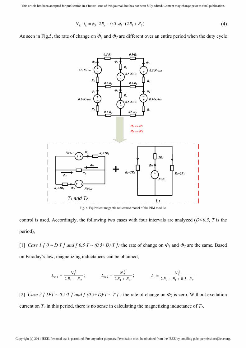
Fig.6 shows an equivalent magnetic model of the PIM module where R1 is the reluctance of the
outer leg of E-core, R2 is the reluctance of I-core and RC represents the reluctance of the center leg of E-
core. RC is much bigger than R1 and R2 due to the air gaps in the center legs. Since the transformers and
the inductor do not affect each other, the equivalent magnetic model can be divided into two parts as
shown in the bottom of Fig.6. The left part represents the magnetic model associated with T1 and T2.
The flux Φ1 and Φ2 will not flow in the center legs of E-core. The flux Φ1 and Φ2 in the shared I-core
might be either partially or fully cancelled depending on the duty cycle D. The right part represents the
magnetic model of the inductor L1.
With assumption that leakage flux through the air is negligible, (2) ~ (4) can be obtained according
to the magnetic model,
22121111 )()2( RRRiN m ⋅−++⋅=⋅ φφφ (2)
21221222 )()2( RRRiN m ⋅−++⋅=⋅ φφφ (3)
t0 t1 t2 t3 t4
VT2
VT1
Ø2Ø1
t0 t1 t2 t3 t4
VT2
VT1
(a) (c)
t0 t1 t2 t3 t4
ΔΦ
VT2
VT1
(b)
Φ1Φ2
ΔΦ
Φ2Φ1 Φ2pk
Φ1pk
-Φ2pk
-Φ1pk
Φ1Pk=Φ2pk
21
2
1 ==NN
K
ΔΦ=0
-Φ1Pk= -Φ2pk
Φ1Pk=Φ2pk
-Φ1Pk= -Φ2pk
11
2
1 ==NN
K21
2
1 ==NN
K
Fig. 5. Excitation voltages of the transformers and their ac flux waveforms when the primary turns factor is K=0.5 under duty cycle control (a); when the primary turns factor is K=1 under duty cycle control (b); when the primary turns factor is K=0.5 under non-duty-cycle control (c).
Copyright (c) 2011 IEEE. Personal use is permitted. For any other purposes, Permission must be obtained from the IEEE by emailing [email protected].
This article has been accepted for publication in a future issue of this journal, but has not been fully edited. Content may change prior to final publication.
)2(5.02 2133 RRRiN cLL +⋅⋅+⋅=⋅ φφ (4)
As seen in Fig.5, the rate of change on Φ1 and Φ2 are different over an entire period when the duty cycle
control is used. Accordingly, the following two cases with four intervals are analyzed (D<0.5, T is the
period),
[1] Case 1 [ 0 ~ D·T ] and [ 0.5·T ~ (0.5+D)·T ]: the rate of change on Φ1 and Φ2 are the same. Based
on Faraday’s law, magnetizing inductances can be obtained,
21
21
1 2 RRNL m +
= ; 21
22
2 2 RRNLm +
= ; 21
2
1 5.02 RRRNL
c
L
⋅++=
[2] Case 2 [ D·T ~ 0.5·T ] and [ (0.5+D)·T ~ T ] : the rate of change on Φ2 is zero. Without excitation
current on T2 in this period, there is no sense in calculating the magnetizing inductance of T2.
+_+ _
+_
+_0.5·NL·iL
+_
+_
+_
+_
0.5·N1·im1
0.5·N2·im2
0.5·N1·im1
0.5·N2·im2
N2·im2
N1·im1
Rc R1>>Rc >> R2
T1 and T2 L1
0.5·NL·iL
NL·iL
Φ1
Φ1
+_
Φ3
Φ2R2
Φ2
R2+2R1
R2+2R1
2Rc
R2+2R1 R2+2R1
0.5·R2 0.5·R2
0.5·R2 0.5·R2
0.5·R2 0.5·R2R1 R1
R1 R1
Rc
Rc
Φ3
Φ3
Φ2 Φ2
Φ1 Φ1
Fig. 6. Equivalent magnetic reluctance model of the PIM module.

Copyright (c) 2011 IEEE. Personal use is permitted. For any other purposes, Permission must be obtained from the IEEE by emailing [email protected].
This article has been accepted for publication in a future issue of this journal, but has not been fully edited. Content may change prior to final publication.
)(2 21
21
1 RRNLm +⋅
= ; 21
2
1 5.02 RRRNL
c
L
⋅++=
For a single separated transformer with the same winding arrangement at the outer leg, the magnetizing
inductance is equal to, Lm=N2/2(R1+R2). As can be seen, such integrated transformers have higher
magnetizing inductances than the single case when both T1 and T2 have excitation (case 1). This is
because of the fact that the flux cancellation occurring in the shared I-core effectively reduces the length
of the transformer flux path. Whereas, there is no improvement on magnetizing inductances if any one
of the transformers has no excitation (case 2).
C. Saturation Consideration
It has been mentioned in the previous section that a saturation problem may appear due to the half
of Φ3 (including dc component) and their overlapping flux together with Φ1 or Φ2 in the right part.
According to Faraday’s law and Ampere’s law, the peak flux densities for each magnetic component in
the PIM module can be derived,
e
FCTpk ANf
VB⋅⋅⋅
=1
1_ 4 (5)
e
FCTpk ANf
DVB⋅⋅⋅
=2
2_ (6)
g
pkLLpk l
INB
⋅⋅= 0
_μ (7)
where f is the switching frequency and Ae is the cross-section of the outer leg of E-core. lg is the total
length of air gaps in the center legs of E-core. In order to avoid flux saturation in the PIM module, the
following equations are required if Bpk_T2 is smaller than Bpk_T1,
satg
pkL
e
FCLpkTpk B
lIN
ANfVBB ≤
⋅⋅+
⋅⋅⋅=+ 0
1_1_ 4
μ (8)
Therefore, one of the drawbacks for the PIM module is a limited power capability. The power capability
of the PIM module can be increased by minimizing the peak flux density of T1, Bpk_T1, which can be
implemented by increasing either the switching frequency or the number of turns. Although both
methods might achieve lower core loss, increased switching frequency contributes to a higher eddy

Copyright (c) 2011 IEEE. Personal use is permitted. For any other purposes, Permission must be obtained from the IEEE by emailing [email protected].
This article has been accepted for publication in a future issue of this journal, but has not been fully edited. Content may change prior to final publication.
current effect in the conductors as well as higher switching loss, and also an increased number of turns
will cause a higher winding loss.
The maximum allowed flux density ripple ΔBL is given by the maximum peak flux density for the
inductor Bpk_L and the ratio of allowed peak-to-peak ripple current (ΔI) to the peak current (Ipk).
pkLpkL I
IBB ΔΔ ⋅= _ (9)
The flux density ripple shall be less than or equal to the maximum allowed value given by (9).
Accordingly the required number of turns is
II
BATVN pk
Lpke
FC
Δ⋅
⋅⋅
≥_4
(10)
High ripple current increases the core loss for the inductor L1, and power loss in the MOSFETs. But low
ripple current requires a high number of inductor turns, which results in high winding loss. Experience
has shown that a good trade-off in high current application is a current ripple factor (Ipk/ΔI) of 2 to 3.
D. Winding Arrangement
Winding losses in transformers increase dramatically with high frequency due to eddy current
effects. Eddy current losses, including skin effect and proximity effect losses seriously impair the
performance of transformers in high-frequency power conversion applications. Both the skin effect and
the proximity effect cause the current density to be non-uniformly distributed in the cross-section of the
conductor, and thus cause a higher winding resistance at higher frequency. The proximity effect loss, in
a multilayer winding, may strongly dominate over the skin effect loss depending on the winding
arrangement. Interleaving transformer windings can reduce the proximity loss significantly when the
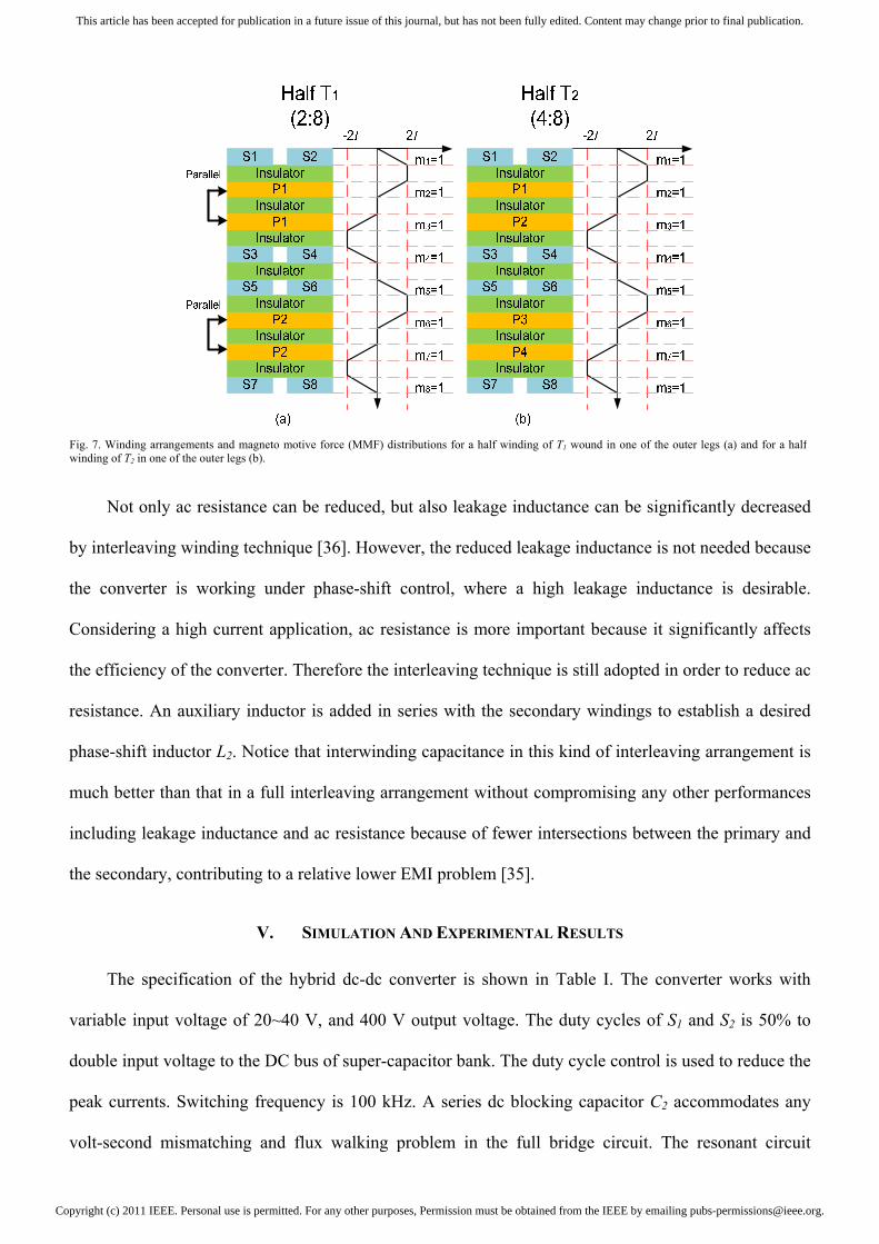
primary and secondary currents are in phase [32]-[34]. Fig.7 shows the winding arrangements and
magneto motive force (MMF) distributions along a vertical direction for a half winding of T1 and T2
wound in one of the outer legs respectively. The value of m [35] in each layer is equal to 1 which
contributes to lower ac resistances.
Copyright (c) 2011 IEEE. Personal use is permitted. For any other purposes, Permission must be obtained from the IEEE by emailing [email protected].
This article has been accepted for publication in a future issue of this journal, but has not been fully edited. Content may change prior to final publication.
Not only ac resistance can be reduced, but also leakage inductance can be significantly decreased
by interleaving winding technique [36]. However, the reduced leakage inductance is not needed because
the converter is working under phase-shift control, where a high leakage inductance is desirable.
Considering a high current application, ac resistance is more important because it significantly affects
the efficiency of the converter. Therefore the interleaving technique is still adopted in order to reduce ac
resistance. An auxiliary inductor is added in series with the secondary windings to establish a desired
phase-shift inductor L2. Notice that interwinding capacitance in this kind of interleaving arrangement is
much better than that in a full interleaving arrangement without compromising any other performances
including leakage inductance and ac resistance because of fewer intersections between the primary and
the secondary, contributing to a relative lower EMI problem [35].
V. SIMULATION AND EXPERIMENTAL RESULTS
The specification of the hybrid dc-dc converter is shown in Table I. The converter works with
variable input voltage of 20~40 V, and 400 V output voltage. The duty cycles of S1 and S2 is 50% to
double input voltage to the DC bus of super-capacitor bank. The duty cycle control is used to reduce the
peak currents. Switching frequency is 100 kHz. A series dc blocking capacitor C2 accommodates any
volt-second mismatching and flux walking problem in the full bridge circuit. The resonant circuit
Fig. 7. Winding arrangements and magneto motive force (MMF) distributions for a half winding of T1 wound in one of the outer legs (a) and for a halfwinding of T2 in one of the outer legs (b).

Copyright (c) 2011 IEEE. Personal use is permitted. For any other purposes, Permission must be obtained from the IEEE by emailing [email protected].
This article has been accepted for publication in a future issue of this journal, but has not been fully edited. Content may change prior to final publication.
consisting of C2 and the primary leakage inductance of T2 is designed to have a resonant frequency
much lower than the switching frequency. A 40 μH auxiliary inductor plus the leakage inductance
obtained on the secondary side of transformers are utilized as the phase-shift inductor L2, which
determines the power as expressed in (1). A good choice for the value of the boost inductor L1 is, as
aforementioned to use a current ripple factor between 2 and 3.
To verify the validity of design approach, a 2D FEA simulation model linked with external
simulation circuit has been built. The simulation parameters fully coincide with the specifications
shown in Table I. Fig.8 shows an instantaneous distribution of the flux density, B, in the core.
Table І Specifications of the hybrid dc-dc converter
Parameters Values
Input voltage VFC (V) 20-40
Output voltage Vo (V) 400
Duty cycle of S1,S2 and S5,S6 0.5
Duty cycle of S3 and S4 0.2-0.5
Switching frequency fs (kHz) 100
DC blocking capacitance C2 (μF) 10
Auxiliary inductor L2 (μH) 40
Boost inductor L1 (μH) 12
Turns ratio of T1 1:4
Turns ratio of T2 1:2
LdcT1 (1:4)
T2 (1:2)
Fig. 8. Instantaneous flux density distribution in the core using 2D FEA simulation.
Copyright (c) 2011 IEEE. Personal use is permitted. For any other purposes, Permission must be obtained from the IEEE by emailing [email protected].
This article has been accepted for publication in a future issue of this journal, but has not been fully edited. Content may change prior to final publication.
Apparently, the right part with a heavy color stress illustrates that half of Φ3 increases the total flux in
the right side together with Φ1 and Φ2. Reversely, the other half of Φ3 decreases the flux in the left part.
A partial flux cancellation on Φ1 and Φ2 occurs in the shared I-core and none of flux Φ3 goes through it.
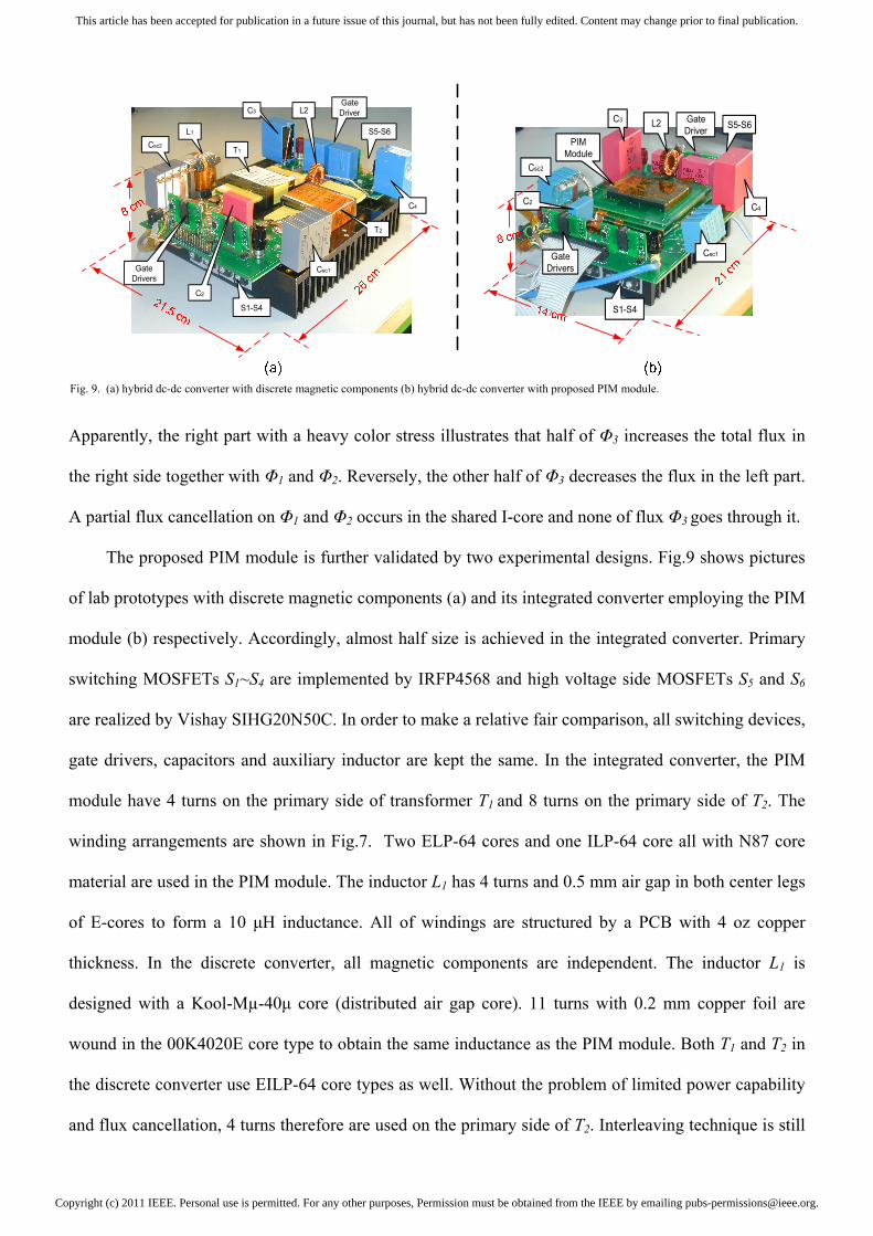
The proposed PIM module is further validated by two experimental designs. Fig.9 shows pictures
of lab prototypes with discrete magnetic components (a) and its integrated converter employing the PIM
module (b) respectively. Accordingly, almost half size is achieved in the integrated converter. Primary
switching MOSFETs S1~S4 are implemented by IRFP4568 and high voltage side MOSFETs S5 and S6
are realized by Vishay SIHG20N50C. In order to make a relative fair comparison, all switching devices,
gate drivers, capacitors and auxiliary inductor are kept the same. In the integrated converter, the PIM
module have 4 turns on the primary side of transformer T1 and 8 turns on the primary side of T2. The
winding arrangements are shown in Fig.7. Two ELP-64 cores and one ILP-64 core all with N87 core
material are used in the PIM module. The inductor L1 has 4 turns and 0.5 mm air gap in both center legs
of E-cores to form a 10 μH inductance. All of windings are structured by a PCB with 4 oz copper
thickness. In the discrete converter, all magnetic components are independent. The inductor L1 is
designed with a Kool-Mµ-40μ core (distributed air gap core). 11 turns with 0.2 mm copper foil are
wound in the 00K4020E core type to obtain the same inductance as the PIM module. Both T1 and T2 in
the discrete converter use EILP-64 core types as well. Without the problem of limited power capability
and flux cancellation, 4 turns therefore are used on the primary side of T2. Interleaving technique is still
S1-S4
Gate Drivers
C2
Csc2
L1
T1
T2
L2
Csc1
C3
C4
S5-S6
Gate Driver
S1-S4
Csc1
Csc2
C2
Gate Drivers
PIM Module
L2
C4
C3 S5-S6Gate Driver
Fig. 9. (a) hybrid dc-dc converter with discrete magnetic components (b) hybrid dc-dc converter with proposed PIM module.
Copyright (c) 2011 IEEE. Personal use is permitted. For any other purposes, Permission must be obtained from the IEEE by emailing [email protected].
This article has been accepted for publication in a future issue of this journal, but has not been fully edited. Content may change prior to final publication.
used to reduce ac resistance. Notice that the transformer windings for the discrete converter are wound
on the center legs of E-cores.
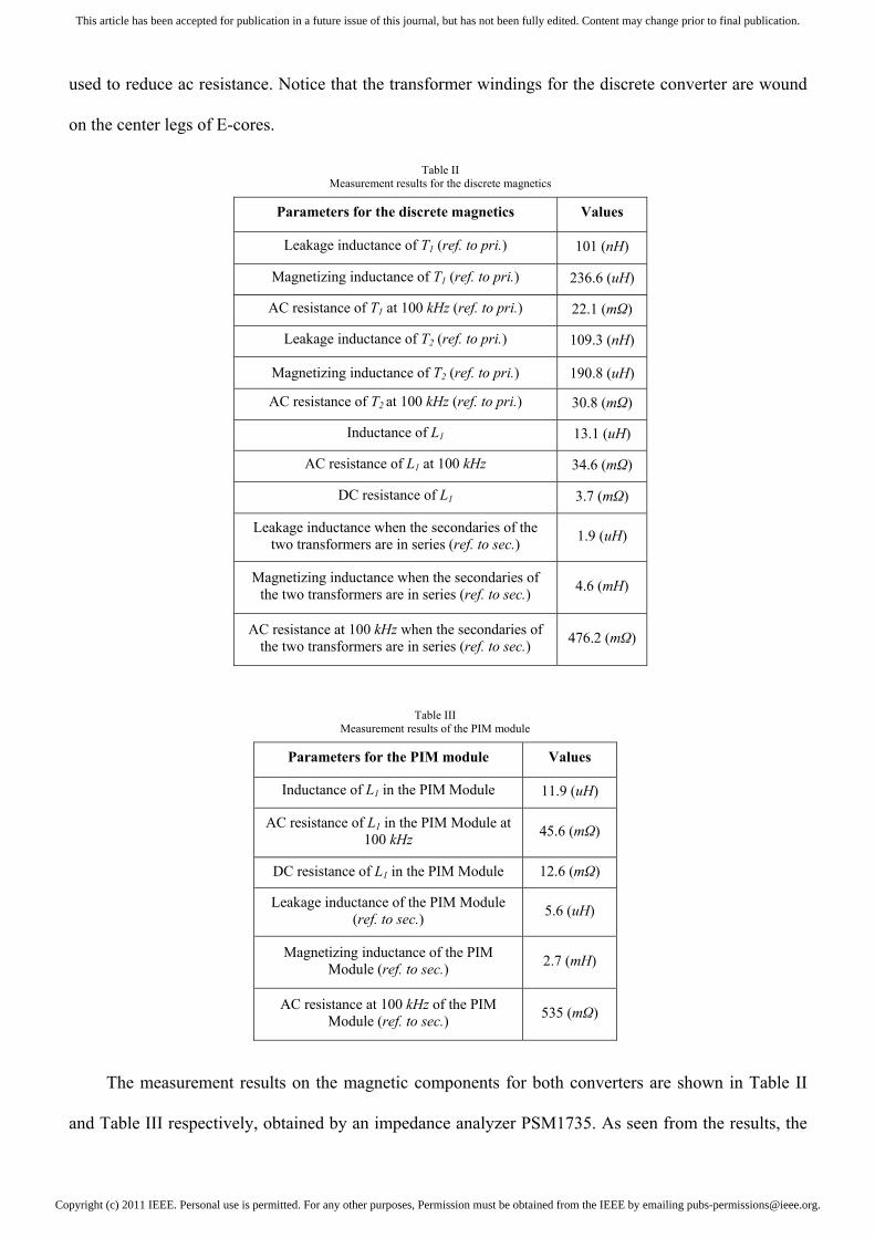
The measurement results on the magnetic components for both converters are shown in Table II
and Table III respectively, obtained by an impedance analyzer PSM1735. As seen from the results, the
Table ІІ Measurement results for the discrete magnetics
Parameters for the discrete magnetics Values
Leakage inductance of T1 (ref. to pri.) 101 (nH)
Magnetizing inductance of T1 (ref. to pri.) 236.6 (uH)
AC resistance of T1 at 100 kHz (ref. to pri.) 22.1 (mΩ)
Leakage inductance of T2 (ref. to pri.) 109.3 (nH)
Magnetizing inductance of T2 (ref. to pri.) 190.8 (uH)
AC resistance of T2 at 100 kHz (ref. to pri.) 30.8 (mΩ)
Inductance of L1 13.1 (uH)
AC resistance of L1 at 100 kHz 34.6 (mΩ)
DC resistance of L1 3.7 (mΩ)
Leakage inductance when the secondaries of the two transformers are in series (ref. to sec.) 1.9 (uH)
Magnetizing inductance when the secondaries of the two transformers are in series (ref. to sec.) 4.6 (mH)
AC resistance at 100 kHz when the secondaries of the two transformers are in series (ref. to sec.) 476.2 (mΩ)
Table ІІI Measurement results of the PIM module
Parameters for the PIM module Values
Inductance of L1 in the PIM Module 11.9 (uH)
AC resistance of L1 in the PIM Module at 100 kHz 45.6 (mΩ)
DC resistance of L1 in the PIM Module 12.6 (mΩ)
Leakage inductance of the PIM Module (ref. to sec.) 5.6 (uH)
Magnetizing inductance of the PIM Module (ref. to sec.) 2.7 (mH)
AC resistance at 100 kHz of the PIM Module (ref. to sec.) 535 (mΩ)

Copyright (c) 2011 IEEE. Personal use is permitted. For any other purposes, Permission must be obtained from the IEEE by emailing [email protected].
This article has been accepted for publication in a future issue of this journal, but has not been fully edited. Content may change prior to final publication.
PIM module has a higher leakage inductance which is due to the fact that the separated windings cause
an imperfect coupling. Furthermore, the higher number of turns on T2 also can be used to explain the
higher leakage inductance [12]. With half cross-section of the center leg, magnetizing inductance in the
PIM module is obviously smaller than that in the discrete magnetics. However, it is worth to notice that
magnetizing inductance in the PIM module is higher than half of the one in the discrete magnetics,
which coincides with the previous analysis in section III. 2.7 mH magnetizing inductance referred to the
secondary side is enough to be used in this application where only 0.44 A magnetizing current ripple is
induced when the converter works in the nominal operation. With regard to ac resistance of the
transformers, a longer winding length, higher number of turns on T2 as well as a few fringing flux
effects may cause a higher value in the PIM module. This contributes almost 1 W more of transformer
winding loss than that in the discrete converter as shown in Table IV.
To facilitate a comparison of the efficiency of the two designs, the losses of major magnetic
components are estimated. The results are tabulated in Table IV for the case when the input voltage is
30 V and the output power is 600 W. Although L1 in the discrete converter has a higher number of turns
which causes a higher ratio of ac resistance to dc resistance due to the proximity effect, the winding loss
of inductor L1 in the discrete converter is much lower than that in the PIM integrated converter as
indicated in the breakdown analysis. This is because a very low dc resistance can be obtained for L1 in
the discrete magnetics due to a thick and wide copper foil, and the dc loss dominates the winding losses
of the inductor. The core loss is evaluated by calculating with the combination of the piecewise linear
Table ІV Loss evaluation breakdown on the magnetic components
for two different prototypes under 30 V input, 600 W output
Loss Discrete Magnetics PIM Module
T1 T2 L1 T1& T2 L1
Winding loss 4.33 W 1.51 W 2.16 W 6.55 W 6.49 W
Total winding loss: 8 W Total winding loss: 13.04 W
Core loss 0.36 W 0.91 W 2.70 W
Total core loss: 1.73 W Total core loss: 3.97 W
Total loss 11.97 W 14.77 W
Copyright (c) 2011 IEEE. Personal use is permitted. For any other purposes, Permission must be obtained from the IEEE by emailing [email protected].
This article has been accepted for publication in a future issue of this journal, but has not been fully edited. Content may change prior to final publication.
model (PWL) and the improved generalized Steinmetz equation (IGSE). The total core loss of the
discrete magnetics is much higher than that of the PIM module. One reason is the distributed air gap
core contributes a relative higher core loss in the discrete magnetics. The other reason is that the flux
cancellation leads to a lower core loss. The authors would like to point out that the size, the winding
loss, the core loss .etc are always in contradiction. A low core loss probably can also be realized in the
discrete magnetics but the size and the winding loss might be compromised. In fact, a real fair
comparison should be built on top of optimized magnetics design. In the present case, the comparison
may not be real fair but it still shows that the PIM module has an advantage on core loss and has an
impressive size deduction.
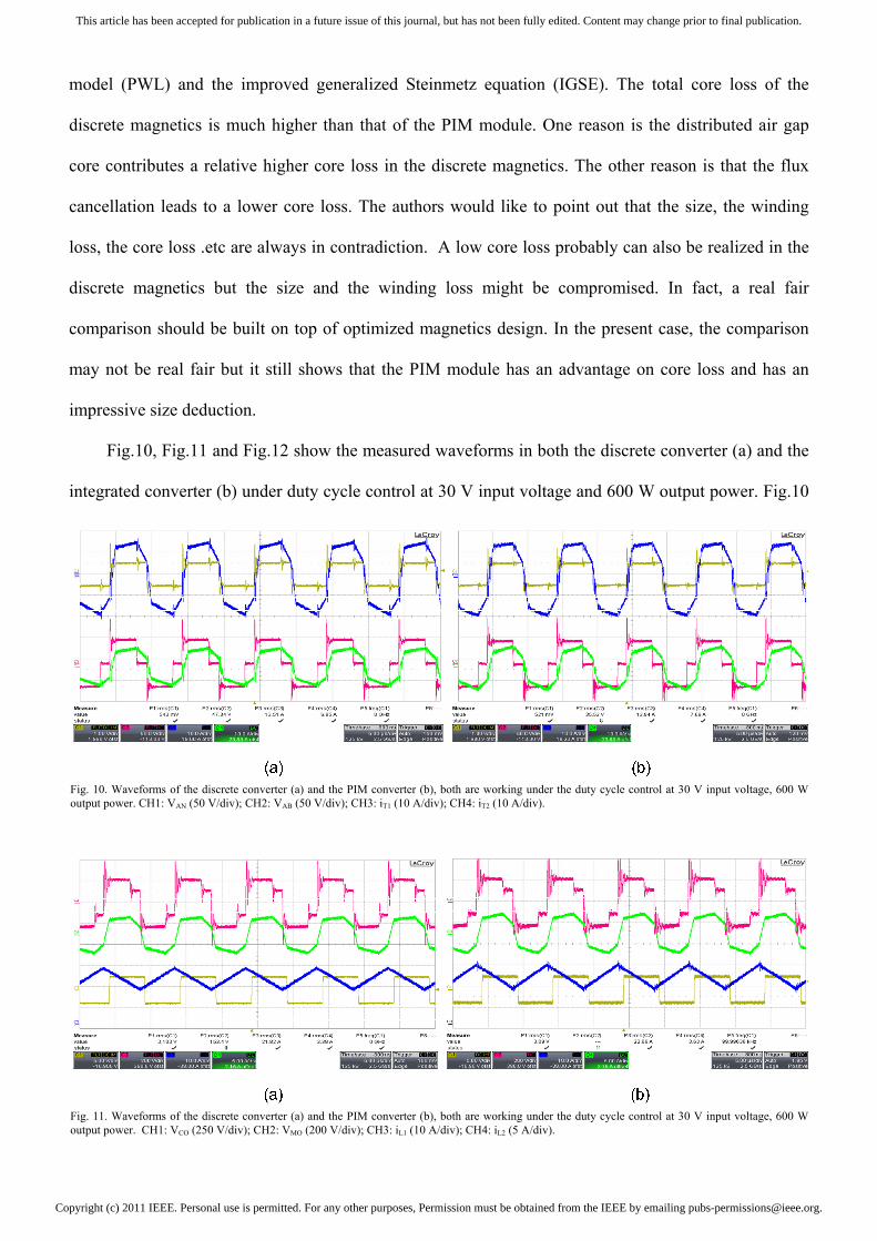
Fig.10, Fig.11 and Fig.12 show the measured waveforms in both the discrete converter (a) and the
integrated converter (b) under duty cycle control at 30 V input voltage and 600 W output power. Fig.10
Fig. 11. Waveforms of the discrete converter (a) and the PIM converter (b), both are working under the duty cycle control at 30 V input voltage, 600 Woutput power. CH1: VCO (250 V/div); CH2: VMO (200 V/div); CH3: iL1 (10 A/div); CH4: iL2 (5 A/div).
Fig. 10. Waveforms of the discrete converter (a) and the PIM converter (b), both are working under the duty cycle control at 30 V input voltage, 600 Woutput power. CH1: VAN (50 V/div); CH2: VAB (50 V/div); CH3: iT1 (10 A/div); CH4: iT2 (10 A/div).
Copyright (c) 2011 IEEE. Personal use is permitted. For any other purposes, Permission must be obtained from the IEEE by emailing [email protected].
This article has been accepted for publication in a future issue of this journal, but has not been fully edited. Content may change prior to final publication.
shows the plots of the primary voltages (CH1: VAN and CH2: VAB) and currents (CH3: iT1 and CH4: iT2)
for T1 and T2 respectively. As can be seen, the peak currents of the transformers have been dropped
during the period of duty cycle control. Fig.11 shows the waveforms of the voltages (CH1: VCO and CH2:
VMO) on the secondary side and currents of the boost inductor (CH3: iL1) and the auxiliary inductor (CH4:
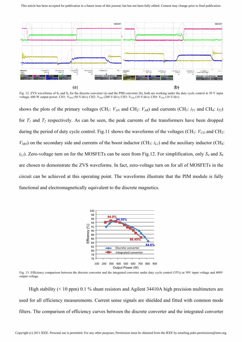
iL2). Zero-voltage turn on for the MOSFETs can be seen from Fig.12. For simplification, only S4 and S6
are chosen to demonstrate the ZVS waveforms. In fact, zero-voltage turn on for all of MOSFETs in the
circuit can be achieved at this operating point. The waveforms illustrate that the PIM module is fully
functional and electromagnetically equivalent to the discrete magnetics.
High stability (< 10 ppm) 0.1 % shunt resistors and Agilent 34410A high precision multimeters are
used for all efficiency measurements. Current sense signals are shielded and fitted with common mode
filters. The comparison of efficiency curves between the discrete converter and the integrated converter
Fig. 12. ZVS waveforms of S4 and S6 for the discrete converter (a) and the PIM converter (b), both are working under the duty cycle control at 30 V inputvoltage, 600 W output power. CH1: VDS4 (50 V/div); CH2: VDS6 (200 V/div); CH3: VGS4 (10 V/div); CH4: VGS6 (10 V/div).
84.6%
767880828486889092949698
100
100 200 300 400 500 600 700 800 900Output Power (W)
Discrete converterIntegrated converter
94.9%94.55%
86.45%
Fig. 13. Efficiency comparison between the discrete converter and the integrated converter under duty cycle control (35%) at 30V input voltage and 400Voutput voltage.

Copyright (c) 2011 IEEE. Personal use is permitted. For any other purposes, Permission must be obtained from the IEEE by emailing [email protected].
This article has been accepted for publication in a future issue of this journal, but has not been fully edited. Content may change prior to final publication.
is shown in Fig.13. The integrated converter has higher efficiency at light load than the discrete
converter. This is due to the fact that the core loss dominates in the total power loss at light load.
Oppositely, the winding loss dominates in the total power loss at heavy load. Therefore a higher
efficiency in the discrete converter can be seen. The results coincide with the aforementioned analysis
and the table breakdown.
VI. CONCLUSION
A new integrated magnetics approach has been proposed in this work. Two transformers and one
inductor are integrated into E-I-E core geometry to reduce the total volume of the converter, core loss
and cost without compromising any electrical performance. The principle of the flux distribution in the
core has been analyzed. Many advantages and disadvantages of the PIM module are included in the
paper. Detail magnetics design consideration of the PIM module including primary turns factor,
magnetic reluctance model, saturation problem and winding arrangement has been investigated in depth.
Two converters with discrete magnetics and integrated magnetics (PIM module) have been built to
demonstrate that the PIM module is fully functional and electromagnetically equivalent. The loss
evaluation has illustrated that there is a core loss reduction in the PIM design. Furthermore, almost half
the size of the discrete converter can be achieved in the integrated converter with the PIM module.
REFERENCES
[1] P. Xu, M. Ye, P. Wong and F. C. Lee, “Design of 48 V voltage regulator modules with a novel integrated magnetics,”
IEEE Trans. on Power Electron., vol.17, no.6, pp.990–998, Nov.2002.
[2] J. Sun, K. F. Webb, and V. Mehrotra, “Integrated magnetics for current-doubler rectifiers,” IEEE Trans. on Power
Electron., vol. 19, no. 3, pp.582-590, May, 2004.
[3] J. Sun, V. Mehrotra, “Orthogonal winding structures and design for planar integrated magnetics,” IEEE Trans. on Ind.
Electron., vol. 55, no. 3, pp.1463-1469, March, 2008.
[4] W. Chen, G. Hua, D. Sable and F. C. Lee, “Design of high efficiency, low profile, low voltage converter with integrated
magnetics,” in Proc. IEEE APEC, 1997, pp. 911-917.
[5] P. Xu, Q. Wu, P. Wong and F. C. Lee, “A novel integrated current doubler rectifier,” in Proc. IEEE APEC, 2000, pp.
735-740.
[6] R. Chen, S. J. T., van Wyk J.D. “Design of planar integrated passive module for zero-voltage-switched asymmetrical
half-bridge PWM converter,” IEEE Trans. on Ind. Appl., Vol. 39, no.36, pp.1648-1655, Nov.-Dec. 2003.
[7] P.A. J. van Rensburg, J.D. van Wyk and J.A. Ferreira, “Design, prototyping and assessment of a 3 kW integrated LCT
component for development in various resonant converters,” IET Power Electron., Vol. 2, no.5, pp.535-544, 2009.

Copyright (c) 2011 IEEE. Personal use is permitted. For any other purposes, Permission must be obtained from the IEEE by emailing [email protected].
This article has been accepted for publication in a future issue of this journal, but has not been fully edited. Content may change prior to final publication.
[8] J. T. Strydom, J. A. Ferreira, J. D. van Wyk, I. W. Hofsajer, E. Waffenschmidt, “Power electronic subassemblies with
increased functionality based on planar sub-components,” in Proc. IEEE PESC, 2000, pp. 1273-1278.
[9] M. J. Prieto, A. M. Pernía, J. M. Lopera, J. Á. Martínez, and F. Nuño, “Turn-Coupling in Thick-Film Integrated
Magnetic Components for Power Converters,” IEEE Trans. on Components and Packaging Technologies, vol.31, no.4,
pp.837–848, Dec.2008.
[10] E. de Jong, J. Ferreira, P. Bauer, “Toward the next level of PCB usage in power electronic converters,” IEEE Trans. on
Power Electron., vol.23, no.6, pp.3153–3163, Nov. 2008.
[11] C. Quinn, K. Rinne, T. O'Donnell, M. Duffy, C.O. Mathuna, “A review of planar magnetic techniques and
technologies,” in Proc. IEEE APEC, 2001, pp. 1175–1183.
[12] C. Buccella, C. Cecati and F. de Monte, “A coupled electrothermal model for planar transformer temperature
distribution computation” IEEE Trans. on Ind. Electron., Vol. 55, no.10, pp.3583-3590, Oct. 2008.
[13] L-P. Wong, Y-S. Lee, M. H. L. Chow, and D. K-W Cheng, “A four-phase forward converter using an integrated
transformer,” IEEE Trans. on Ind. Electron., vol. 55, no. 2, pp.817-831, March, 2008.
[14] S-Y Lee, A. G. Pfaelzer, and J. D. van Wyk, “Comparison of different designs of a 42-V/14-V dc/dc converter regarding
losses and thermal aspects” IEEE Trans. on Ind. Appl., vol.43, no.2, pp.520–530, Mar.2007.
[15] P-L. Wong, Q-Q. Wu, P. Xu, B. Yang and F. C. Lee, “Investigating coupling inductors in the interleaving QSW VRM,”
in Proc. IEEE APEC, 2000, pp. 973-978.
[16] H. Kosai, S. McNeal, B. Jordan, J. Scofield, B. Ray and Z. Turgut, “Coupled inductor characterization for a high
performance interleaved boost converter,” IEEE Trans. on Magn., vol.45, no.10, pp.4812–4815, Oct.2009.
[17] L. Yan and B. Lehman, “An integrated magnetic isolated two-inductor boost converter: analysis, design and
experimentation” IEEE Trans. on Power Electron., vol.20, no.2, pp.332–342, Mar.2005.
[18] Z-W. Ouyang, O. C. Thomsen, M. A. E. Andersen, “New geometry integrated inductors in two-channel interleaved
bidirectional converter,” in Proc. IEEE IECON, 2010. pp. 582-586.
[19] A. Payman, S. Pierfederici and F. M. Tabar, “Energy management in a fuel cell/supercapacitor multisource/multiload
electrical hybrid system,” IEEE Trans. Power Electron., vol. 24, no. 12, pp. 2681-2691, 2009.
[20] W-S. Liu, J-F. Chen, T-J. Liang, R-L. Lin and C-H. Liu, "Analysis, design, and control of bidirectional cascaded
configuration for a fuel cell hybrid power system," IEEE Trans. on Power Electron., vol.25, no.6, pp.1565-1575, June
2010.
[21] M. Nymand, R. Tranberg, M. E. Madsen, U. K. Madawala and M. A. E. Andersen, “What is the best converter for low
voltage fuel cell applications-A buck or boost,” in Proc. IEEE IECON, 2009, pp. 959-964.
[22] Z. Zhang, O. C. Thomsen and M. A. E. Andersen, “Wide input voltage range bidirectional DC-DC converter for fuel
cell and supercapacitor in UPS system,” in Proc. IEEE PEDS, 2009, pp.706-711.
[23] D. Xu, C. Zhao and H. Feng, “A PWM plus phase-shift control bidirectional DC–DC converter,” IEEE Trans. on Power
Electron., vol.19, no.3, pp.666–675, May.2004.
[24] J. Wang, F.Z. Peng, J.Anderson, A.Joesph and R. Buffenbarger, “Low cost fuel cell converter system for residential
power generation,” IEEE Trans. on Power Electron., Vol. 19, no.5, pp.1315-1322, Sep. 2004.
[25] Y. Jang and M.M. Jovanovic´, “A new PWM ZVS full-bridge converter,” IEEE Trans. on Power Electron., Vol.
22, no.3, pp.987-994, May. 2007.
[26] D. Liu and H. Li., “A ZVS bi-directional DC–DC converter for multiple energy storage elements,” IEEE Trans. on
Power Electron., Vol. 21, no.5, pp.1513-1517, Sept. 2006.
[27] H. Tao; A. Kotsopoulos, J.L. Duarte, M.A.M. Hendrix, “Transformer-coupled multiport ZVS bidirectional DC–DC
converter with wide input range,” IEEE Trans. on Power Electron., Vol. 23, no.2, pp.771-781, March. 2008.

Copyright (c) 2011 IEEE. Personal use is permitted. For any other purposes, Permission must be obtained from the IEEE by emailing [email protected].
This article has been accepted for publication in a future issue of this journal, but has not been fully edited. Content may change prior to final publication.
[28] Z-W. Ouyang, Z. Zhang, O. C. Thomsen, M. A. E. Andersen, O. Poulsen and T. Björklund, “Planar integrated
magnetics design in wide input range dc-dc converter for fuel cell application,” in Proc. IEEE ECCE, 2010. pp. 4611-
4618.
[29] G. Sen, Z-W. Ouyang, O. C. Thomsen and M. A. E. Andersen, “A high efficient integrated planar transformer for
primary-parallel isolated boost converters,” in Proc. IEEE ECCE, 2010. pp. 4605-4610.
[30] Z-W. Ouyang, G. Sen, O. C. Thomsen, M. A. E. Andersen, “Fully integrated planar magnetics for primary-parallel
isolated boost converter,” in Proc. IEEE APEC, 2011.
[31] K. Venkatachalam, C. R. Sullivan, T. Abdallah, and H. Tacca, “Accurate prediction of ferrite cores loss with
nonsinusoidal waveforms using only Steinmetz parameters,” in Proc. IEEE Workshop Comput. Power Electron., Jun. 3–
4, 2002, pp. 36–41.
[32] J. Ferreira, “Improved analytical modeling of conductive losses in magnetic components,” IEEE Trans. on Power
Electron., vol. 9, no. 1, pp. 127–131, Jan. 1994.
[33] W. G. Hurley, E. Gath, J. G. Breslin, “Optimizing the AC resistance of multilayer transformer windings with arbitrary
current waveforms,” IEEE Trans. on Power Electron., vol.15, no.2, pp.369–376, Mar. 2008.
[34] X. Nan, C. R. Sullivan, “An improved calculation of proximity-effect loss in high-frequency windings of round
conductors,” in Proc. IEEE PESC, 2003, pp.853–860.
[35] Z-W. Ouyang, O. C. Thomsen and M. A. E. Andersen, “Optimal analysis and improved design of planar transformer in
high power dc-dc converters” IEEE Trans. on Ind. Elec., 2011.
[36] Z-W. Ouyang, O. C. Thomsen and M. A. E. Andersen, “The analysis and comparison of leakage inductance in
different winding arrangements for planar transformer,” in Proc. IEEE PEDS, 2009, pp. 1143 – 1148.