Embed Size (px)
Citation preview

PL10S-W12C, PL10SMS-W12C
Page 1
NON-ISOLATED DC-DC Converter
6.0-14Vin, 0.75- 5.0Vout, 10A
INSTALLATION / APPLICATION NOTE
PL10S-W12C PL10SMS-W12C

PL10S-W12C, PL10SMS-W12C
Page 2
Content1. INTRODUCTION 3
2. CONVERTER FEATURES 3
3. GENERAL DESCRIPTION 33.1 Electrical Description 3
3.2 Thermal Packaging and Physical Design 3
4. TECHNICAL SPECIFICATIONS 4
5. MAIN FEATURES AND FUNCTIONS 65.1 Operating Temperature Range 6
5.2 Over-Temperature Protection (OTP) 6
5.3 Output Voltage Adjustment 6
5.4 Safe Operating Area (SOA) 6
5.5 Over Current Protection 6
5.6 Remote ON/OFF 6
5.7 UVLO (Under-Voltage Lockout) 7
5.8 Output Voltage Tracking (Sequencing) 7
6. SAFETY 86.1 Input Fusing and Safety 8
7. APPLICATIONS 87.1 Layout Design 8
7.2 Convection Cooling 9
7.3 Thermal Considerations 9
7.4 Power De-Rating Curves 10
7.5 Efficiency vs Load Curves 13
7.6 Input Capacitance 16
7.7 Test Set-Up 16
7.8 Remote Sense Compensation 16
7.9 Output Voltage Adjustment 17
7.10 Output Ripple and Noise Measurement 17
7.11 Output Capacitance 17
7.12 PL10SMS Reflow Profile 17
8. MECHANICAL 188.1 Outline Diagrams 18
8.2 SMS Tape and Reel Dimensions 18

PL10S-W12C, PL10SMS-W12C
Page 3
1. IntroductionThis application note describes the features and functions of Lambda’sPL10S-W12C and PL10SMS-W12C series of Non Isolated DC-DCConverters. These “Point of Load” modules serve the needs specificallyof the fixed and mobile telecommunications and computing markets.Capable of operating over a wide input voltage range of 6.0 – 14VDC,this series provides a precise regulated output voltage within the rangeof 0.7525 to 5.0 Vdc. The operating ambient temperature range is –40°C to +85°C. Ultra-high efficiency operation is achieved through theuse of synchronous rectification. The modules are protected againstshort circuit and over-temperature conditions.
2. Converter Features• High efficiency, typically 95% at 5.0Vdc• Industry standard footprint• Wide ambient temperature range, -40°C to +85°C• Cost efficient open frame design• Programmable output voltage via external resistor from 0.7525 to
5.0Vdc• No minimum load requirement (stable at all loads)• Remote ON/OFF• Remote sense compensation• Fixed switching frequency• Continuous short-circuit protection and over current protection• Over-temperature protection (OTP)• Monotonic Startup with pre-bias at the output.• UL/IEC/EN60950 Certified.• Output Voltage Sequencing (Tracking )• Power Good Signal (Optional)
3. General Description3.1 Electrical Description
A block diagram of the converter is shown in Figure 1. The topology isbased on a non-isolated synchronous buck converter. The control loopis optimized for stability, fast transient response, and very tight line andload regulation. In a typical pre-bias application the converters do notdraw any reverse current at start-up. The output voltage can beadjusted from 0.7525 to 5.0 Vdc using the TRIM pin with an externalresistor. The converter can be shut down via a remote ON/OFF inputthat is referenced to ground. This input is compatible with readilyavailable logic devices. A 'positive' logic input is supplied as standard.Positive logic implies that the converter is enabled if the remoteON/OFF input is high (or floating), and disabled if it is low.
The converter is protected against over-temperature conditions. If theconverter is overloaded or the temperature of the converter exceeds itsspecified operating range, the converter will shut down and re-startonce the fault condition is removed.
C1 C2Q2
Q1
D1
L1+VIN
COM COM
+VO
PWM ICR1
R2
R sense
R trimERR AMPON/OFF TRIM
+SENSE
SEQ
PGood
Figure 1. Electrical Block Diagram
3.2 Thermal Packaging and Physical Design
The converter uses a multi-layer FR4 PCB construction. All surfacemount power components are placed on one side of the PCB, and alllow-power control components are placed on the opposite side; thus,the heat dissipation of the power components is optimized, ensuringthat control components are not thermally stressed. The converter is anopen-frame product and has no case or case pin. The open-framedesign has several advantages over encapsulated closed devices;among these advantages are:
• Efficient Thermal Management: The heat is removed from theheat generating components without affecting sensitive smallsignal control components.
• Environmental: Lead free open-frame converters are more easilyre-cycled.
• Cost Efficient: No encapsulation. Cost efficient open-frameconstruction.
• Reliable: Efficient cooling provided by open frame construction,offers high reliability.

PL10S-W12C, PL10SMS-W12C
Page 4
4. Technical Specifications(All specifications are typical at nominal input, full load at 25°C unless otherwise noted.)
PARAMETER NOTES and CONDITIONS Device Min. Typical Max. Units
Operating Temperature ALL -40 +85 °CStorage Temperature ALL -55 +125 °C
Input Voltage Vo.75 to 4.5VVo 5.0V
6.06.5
1212
1414 Vdc
Input Under-Voltage LockoutTurn-On Voltage Threshold ALL 5.0 VdcTurn-Off Voltage Threshold ALL 4.0 VdcLockout Hysteresis Voltage ALL 1.0 Vdc
Maximum Input Current Vin=0 to 14Vdc, Io = Io max. ALL 10 A
No-Load Input Current
Vo = 0.7525VVo = 1.2VVo = 1.5VVo = 1.8VVo = 2.0VVo = 2.5VVo = 3.3VVo = 5.0V
ALL
4040505060657595
mA
Input Current Converter disabled (shut down) ALL 10 mA
Inrush Current (I2t) ALL 0.4 A2s
Input Reflected-Ripple Current P-P thru 1uH inductor, 5Hz to 20MHz ALL 200 mA
Output Voltage Set Point Vin = Nominal Vin , Io = Io max, Tc=25°C ALL -1.5% Vo,set +1.5% VdcOutput Voltage Trim Adjustment Range Selected by an external resistor ALL 0.7525 5.0 VdcOutput Voltage Regulation
Load Regulation Io = Io min to Io max ALL -0.5 +0.5 %Line Regulation Vin = low line to high line ALL -0.2 +0.2 %
Temperature Coefficient Ta = -40°C to 85°C ALL -0.03 +0.03 %/°COutput Voltage Ripple and Noise 5Hz to 20MHz bandwidth
Peak-to-Peak Full Load, 1uF ceramic and 10uF tantalum ALL 75 mVRMS Full Load, 1uF ceramic and 10uF tantalum ALL 30 mV
External Capacitive Load Low ESR ALL 8000 uFOperating Output Current Range ALL 0 10 AOutput DC Current-Limit Inception Output Voltage = 90% Nominal Output Voltage ALL 15 20 25 AShout Circuit Protection Continuous with Hiccup ModeSequencing Slew Rate Capability dVSEQ/dt 0.1 1.0 V/msSequencing Delay Time 10 ms
Tracking Accuracy Power upPower down ALL 200
400 mV
Power Good Signal Asserted Logic High Vo Suffix “P” 90 110 %
Output Voltage Transient Response
Error Brand 50% Step Load Change, di/dt=2.5A/us ALL 200 mV
Setting Time (within 1% Vout nominal) 50% Step Load Change, di/dt=2.5A/us ALL 200 us
Efficiency
100% Load
Vo = 0.7525VVo = 1.2VVo = 1.5VVo = 1.8VVo = 2.0VVo = 2.5VVo = 3.3VVo = 5.0V
ALL
8287899091929395
%

PL10S-W12C, PL10SMS-W12C
Page 5
Isolation
Input to Output Non-isolation ALL 0 Vdc
Switching Frequency ALL 300 KHz
ON/OFF Control, Positive Logic Remote On/OffLogic Low (Module Off)Logic High (Module On) or Open Circuit
PL10S-W12CPL10S-W12CP
PL10SMS-W12CPL10SMS-W12CP
0 0.4Vin
VdcVdc
ON/OFF Control, Negative Logic Remote On/OffLogic Low (Module On)Logic High (Module Off)
or Open Circuit
PL10S-W12CNPL10S-W12CNP
PL10SMS-W12CNPL10SMS-W12CNP
02.8
0.4Vin
VdcVdc
ON/OFF Current (for both remote on/off logic) Ion/off at Von/off = 0.0V ALL 1 mALeakage Current (for both remote on/off logic) Logic High, Von/off = 14V ALL 1 mA
Turn-On Delay and Rise TimeTurn-On Delay Time, From On/Off Control Von/off to 10%Vo,set ALL 3 msTurn-On Delay Time, From Input Vin,min. to 10%Vo,set ALL 3 msOutput Voltage Rise Time 10%Vo,set to 90%Vo,set ALL 4 ms
Over Temperature Protection ALL 130 %General Specifications
MTB F Io = 100% of Io max; Ta = 25°C per MIL-HDBK-217F ALL 0.92 M hours
Weight ALL 8.5 gramsDimensions
SIP packages 2 x 0.51 x 0.327 inches (50.8x12.95x8.3 mm)SMS packages 1.3 x 0.53 x 0.346 inches (33.0x13.46x8.8 mm)

PL10S-W12C, PL10SMS-W12C
Page 6
5. Main Features and Functions5.1 Operating Temperature Range
The converters operate over a wide ambient temperature environment ( -40°C to 85°C). Due consideration must be given to the de-rating curveswhen determining the maximum power that can be drawn from theconverter. The maximum power drawn is influenced by a number offactors, such as:• Input voltage range• Output load current• Air velocity (forced or natural convection)• Mounting orientation of converter PCB with respect to the Airflow• Motherboard PCB design, especially ground and power planes;
these can be effective heat sinks for the converter.
5.2 Over-Temperature Protection (OTP)
The converters are equipped with non-latching over-temperatureprotection. A temperature sensor is located at the hottest point within theconverter; typically, the on top of the switching device. If the temperatureexceeds a threshold of 130°C (typical) the converter will shut down,disabling the output. When the temperature has decreased to a safeoperating range, the converter will automatically start.The over-temperature condition can be induced by a variety of reasonssuch as external overload condition or a system fan failure.
5.3 Output Voltage Adjustment
Section 7.8 describes in detail how to trim the output voltage with respectto its set point. The output voltage on all models is adjustable over therange of 0.7525 – 5.0Vdc.
5.4 Safe Operating Area (SOA)
Figure 2 provides a graphical representation of the Safe Operating Area(SOA) of the converter. This representation assumes ambient operatingconditions such as airflow are met as per thermal guidelines provided inSections 7.2 and 7.3.
Vo
IoIo,CLIo,max
Vo,nom
Safe Operating Area
CURRENT (A)
VO
LTA
GE
(V)
Figure 2. Maximum Output Current Safe Operating Area
5.5 Over Current Protection
All models have short-circuit and over current protection. The converterwill automatically recover once either condition is removed. It will alsosupply up to 150% of it rated output current. In the event of an over-current condition the converter will go into a hiccup mode.
5.6 Remote ON/OFF
Positive Logic- The remote ON/OFF input feature of the converterallows external circuitry to turn the converter ON or OFF. Active-highremote ON/OFF is available as standard. The converters are turned ‘on’if the remote ON/OFF pin is high (=Vin), or left open. Setting the pin low(<0.4Vdc) will turn the converter ‘off’’. The signal level of the remoteon/off input is defined with respect to ground. If remote on/off is notneeded, leave the remote on/off pin disconnected and the module will beon.Negative Logic- Designated with a suffix “N” is the Negative remoteON/OFF version. The unit is ‘off’ if this voltage level is above 2.8Vdc.The converter is ‘on’ if the on/off pin input is low (<0.4Vdc) or left open.The recommended remote on/off drive circuits are shown in figures 3 and4.
Figure 3. Positive Remote ON/OFF Input Drive Circuit
Figure 4. Negative Remote ON/OFF Input Drive Circuit
Q1
ON/OFF
Control
+Vin +Vo
RemoteON/OFF
CommonCommon
Q1
ON/OFFControl
+Vin
RemoteON/OFFCommon Common
+Vo

PL10S-W12C, PL10SMS-W12C
Page 7
5.7 UVLO (Under-Voltage Lockout)
When the input Vcc rises above 5.0V, the converter initiates a soft start.The UVLO function in the converter has a hysteresis of approximately1volt to provide noise immunity at start-up.
5.8 Output Voltage Tracking (Sequencing)
The converters have a tracking feature that is available via the pinlabeled ‘SEQ’. When this feature is not used, this pin should be tied to+Vin. When this feature is used, the on/off pin should be leftdisconnected so that the converter is on by default.The tracking feature (sequencing) is used with two or more converters inapplications where one output voltage is required to be in regulationbefore another. When the output voltage from the ‘master’ is applied tothe SEQ pin of the ‘slave’, the output voltage of the ‘slave’ tracks theoutput voltage of the ‘master’ until the slave reaches its output voltageset point. The ‘master’ output voltage must be higher than the ‘slave’.A valid input voltage must be maintained until the tracking and outputvoltages reach ground potential to ensure a controlled shutdown of themodules, when using the remote on/off on the ‘master’.A typical circuit example with one converter being used as a ‘master’ anda second converter being used as a ‘slave’ is shown below:
+Vin
Common Common
+Vo
+Vin
SEQ
Common Common
+Vo
Converter (slave)
+PowerR1Load
R2Load
CH1C1
Supply
CH2C2 CH3
Converter (master)
Figure 5. Sequencing Test Circuit
Power start up with SEQ signalInput Voltage=12VdcMaster DC/DC output voltage (CH1) = 5VdcSlave DC/DC output voltage (CH2)=3.3VdcSequencing voltage= 0.6V/msec
Figure 6. Sequencing Test Circuit
Power turn off with SEQ signal voltageInput Voltage=12Vdc (CH1)Master DC/DC output voltage (CH2) = 5VdcSlave DC/DC output voltage (CH3)=3.3Vdc
Figure 7. Sequencing Test Circuit

PL10S-W12C, PL10SMS-W12C
Page 8
6. Safety
6.1 Input Fusing and Safety
These products are approved to UL 60950-1:2003, CAN/CSA C22.2NO.60950-1:2003 and IEC/EN60950-1:2001.These products are designed to be PCB mounted and for use withinother equipment or enclosures. For safe installation and operation,carefully follow the instructions below:
Do not install, test, or operate the products near water or spill liquid onthem.Do not operate these products unless they are securely fastened.These products must be installed in a restricted access locationaccessible to authorized personnel only.These products must be professionally installed in accordance with theprevailing electrical wiring regulations and safety standards.The output power taken from the unit must not exceed the ratings statedin the catalog datasheet.Ensure adequate ventilation is provided to allow air to circulate.This product has functional insulation between input and output andtherefore the DC source to this product must be reinforced or doubleinsulated to the AC input in accordance with IEC/EN 60950-1 to achieveSELV output.Fusing – External ceramic sand-filled fuse, 250V, F20A, HBC.
7. Applications
7.1 Layout Design
In optimizing thermal design the PCB is utilized as a heat sink. Someheat is transferred from the module to the main board through connectingpins. The system designer or the end user must ensure that othercomponents and metal in the vicinity of the converter meet the spacingrequirements to which the system is approved.Low resistance and low inductance PCB layout traces are the norm andshould be used where possible. Consideration must also be given toproper low impedance traces between the power module and input /output grounds. The recommended footprints are shown in figures 8 and9.
All Dimensions in Inches(mm)Tolerance : .XX= ¡Ó0.04 .XXX= ¡Ó0.010
LAYOUT PATTERNTOP VIEW
0.33(8.4)0.29(7.4)
1.1mm PLATED THROUGH HOLE1.6mm PAD SIZE
Figure 8. Recommended PL10S Footprint
+S E NSE TR IM +VO C OM
ON /OFF +VIN
7.544.83 4.83 4.83
3.05
10.92
0.64
10.29
(0.297)
(0 .190) (0.190) (0 .190)
(0 .120)
(0 .405)
(0 .025)(1.177)
(0.430)
29.90
P A D S IZEM IN:3.556 x2.413(0.140 x0.095)M AX :4.19x2.79(0.165x0.110)
D im ensions are in m illim eters and(inches)
R ec om m ended P ad Layou t
Top V iew of B oard
S E QPGood
4.83
(0.190)
4.83
(0.190)
Figure 9. Recommended PL10SMS Footprint

PL10S-W12C, PL10SMS-W12C
Page 9
7.2 Convection Cooling
To predict the approximate cooling needed for the module, refer to thePower De-rating curves in Figures 13 and 14. These de-rating curves areapproximations of the ambient temperatures and airflows required tokeep the power module temperature below its maximum rating. Once themodule is assembled in the actual system, the module’s temperatureshould be checked as shown in Figure 10 to ensure it does not exceed115°C.Proper cooling can be verified by measuring the power module’stemperature at “ Tref ” as shown in Figures 11 and 12.
Note: Dimensions are in millimeters and (inches)
Figure 10. Thermal Test Setup
Figure 11. Temperature Measurement Location for PL10S
Figure 12. Temperature Measurement Location for PL10SMS
7.3 Thermal Considerations
The power module operates in a variety of thermal environments;however, sufficient cooling should be provided to help ensure reliableoperation of the unit. Heat is removed by conduction, convection, andradiation to the surrounding environment. The thermal data presented isbased on measurements taken in a set-up as shown in Figure 10.Figures 13 and 14 represent the test data. Note that the airflow is parallelto the long axis of the module as shown in Figure 7 for the converters.The temperature at “ Tref ” location should not exceed 115 °C. Theoutput power of the module should not exceed the rated power for themodule (VO, set x IO, max). The thermal data presented is based onmeasurements taken in a wind tunnel.
25.4(1.0)
12.7(0.5)
76.2(3.0)
Power Module
Air flow
Thermocuple Locationfor measuringambient temperatureand airflow
PWBs
Wind Tunnel
PL10S-W12C, PL10SMS-W12C
Page 10
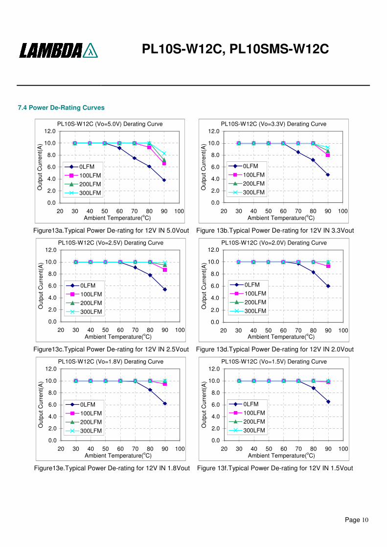
7.4 Power De-Rating Curves
PL10S-W12C (Vo=5.0V) Derating Curve
0.0
2.0
4.0
6.0
8.0
10.0
12.0
20 30 40 50 60 70 80 90 100Ambient Temperature(oC)
Out
put C
urre
nt(A
)
0LFM100LFM200LFM300LFM
PL10S-W12C (Vo=3.3V) Derating Curve
0.0
2.0
4.0
6.0
8.0
10.0
12.0
20 30 40 50 60 70 80 90 100Ambient Temperature(oC)
Out
put C
urre
nt(A
)
0LFM100LFM200LFM300LFM
Figure13a.Typical Power De-rating for 12V IN 5.0Vout Figure 13b.Typical Power De-rating for 12V IN 3.3Vout
PL10S-W12C (Vo=2.5V) Derating Curve
0.0
2.0
4.0
6.0
8.0
10.0
12.0
20 30 40 50 60 70 80 90 100Ambient Temperature(oC)
Out
put C
urre
nt(A
)
0LFM100LFM200LFM300LFM
PL10S-W12C (Vo=2.0V) Derating Curve
0.0
2.0
4.0
6.0
8.0
10.0
12.0
20 30 40 50 60 70 80 90 100Ambient Temperature(oC)
Out
put C
urre
nt(A
)
0LFM100LFM200LFM300LFM
Figure13c.Typical Power De-rating for 12V IN 2.5Vout Figure 13d.Typical Power De-rating for 12V IN 2.0Vout
PL10S-W12C (Vo=1.8V) Derating Curve
0.0
2.0
4.0
6.0
8.0
10.0
12.0
20 30 40 50 60 70 80 90 100Ambient Temperature(oC)
Out
put C
urre
nt(A
)
0LFM100LFM200LFM300LFM
PL10S-W12C (Vo=1.5V) Derating Curve
0.0
2.0
4.0
6.0
8.0
10.0
12.0
20 30 40 50 60 70 80 90 100Ambient Temperature(oC)
Out
put C
urre
nt(A
)
0LFM100LFM200LFM300LFM
Figure13e.Typical Power De-rating for 12V IN 1.8Vout Figure 13f.Typical Power De-rating for 12V IN 1.5Vout

PL10S-W12C, PL10SMS-W12C
Page 11
PL10SMS-W12C (Vo=1.2V) Derating Curve
0.0
2.0
4.0
6.0
8.0
10.0
12.0
20 30 40 50 60 70 80 90 100Ambient Temperature(oC)
Out
put C
urre
nt(A
)
0LFM100LFM200LFM300LFM
PL10SMS-W12C (Vo=0.75V) Derating Curve
0.0
2.0
4.0
6.0
8.0
10.0
12.0
20 30 40 50 60 70 80 90 100Ambient Temperature(oC)
Out
put C
urre
nt(A
)
0LFM100LFM200LFM300LFM
Figure13g.Typical Power De-rating for 12V IN 1.2Vout Figure 13h.Typical Power De-rating for 12V IN 0.75Vout
PL10SMS-W12C (Vo=5.0V) Derating Curve
0
2
4
6
8
10
12
20 30 40 50 60 70 80 90 100Ambient Temperature(oC)
Out
put C
urre
nt(A
)
0LFM100LFM200LFM300LFM
PL10SMS-W12C (Vo=3.3V) Derating Curve
0
2
4
6
8
10
12
20 30 40 50 60 70 80 90 100Ambient Temperature(oC)
Out
put C
urre
nt(A
)
0LFM100LFM200LFM300LFM
Figure14a.Typical Power De-rating for 12V IN 5.0Vout Figure 14b.Typical Power De-rating for 12V IN 3.3Vout
PL10SMS-W12C (Vo=2.5V) Derating Curve
0
2
4
6
8
10
12
20 30 40 50 60 70 80 90 100Ambient Temperature(oC)
Out
put C
urre
nt(A
)
0LFM100LFM200LFM300LFM
PL10SMS-W12C (Vo=2.0V) Derating Curve
0
2
4
6
8
10
12
20 30 40 50 60 70 80 90 100Ambient Temperature(oC)
Out
put C
urre
nt(A
)
0LFM100LFM200LFM300LFM
Figure14c.Typical Power De-rating for 12V IN 2.5Vout Figure 14d.Typical Power De-rating for 12V IN 2.0Vout
PL10S-W12C, PL10SMS-W12C
Page 12
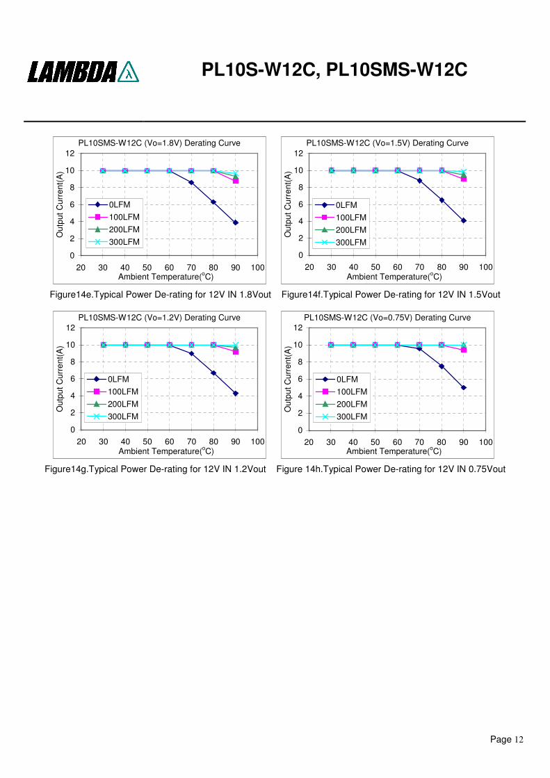
PL10SMS-W12C (Vo=1.8V) Derating Curve
0
2
4
6
8
10
12
20 30 40 50 60 70 80 90 100Ambient Temperature(oC)
Out
put C
urre
nt(A
)
0LFM100LFM200LFM300LFM
PL10SMS-W12C (Vo=1.5V) Derating Curve
0
2
4
6
8
10
12
20 30 40 50 60 70 80 90 100Ambient Temperature(oC)
Out
put C
urre
nt(A
)
0LFM100LFM200LFM300LFM
Figure14e.Typical Power De-rating for 12V IN 1.8Vout Figure14f.Typical Power De-rating for 12V IN 1.5Vout
PL10SMS-W12C (Vo=1.2V) Derating Curve
0
2
4
6
8
10
12
20 30 40 50 60 70 80 90 100Ambient Temperature(oC)
Out
put C
urre
nt(A
)
0LFM100LFM200LFM300LFM
PL10SMS-W12C (Vo=0.75V) Derating Curve
0
2
4
6
8
10
12
20 30 40 50 60 70 80 90 100Ambient Temperature(oC)
Out
put C
urre
nt(A
)
0LFM100LFM200LFM300LFM
Figure14g.Typical Power De-rating for 12V IN 1.2Vout Figure 14h.Typical Power De-rating for 12V IN 0.75Vout

PL10S-W12C, PL10SMS-W12C
Page 13
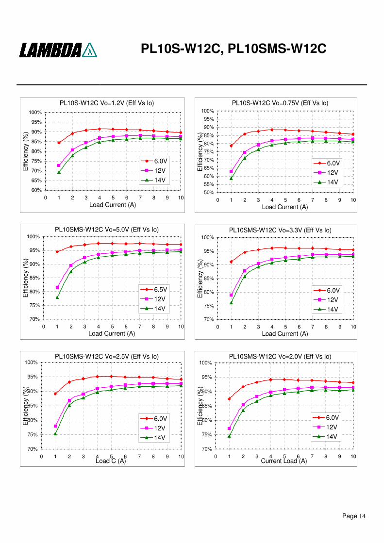
7.5 Efficiency vs Load Curves
PL10S-W12C Vo=5.0V (Eff Vs Io)
70%
75%
80%
85%
90%
95%
100%
0 1 2 3 4 5 6 7 8 9 10Load Current (A)
Effi
cien
cy (%
)
6.5V12V14V
PL10S-W12C Vo=3.3V (Eff Vs Io)
70%
75%
80%
85%
90%
95%
100%
0 1 2 3 4 5 6 7 8 9 10Load Current (A)
Effi
cien
cy (%
)
6.0V12V14V
PL10S-W12C Vo=2.5V (Eff Vs Io)
70%
75%
80%
85%
90%
95%
100%
0 1 2 3 4 5 6 7 8 9 10Load Current (A)
Effi
cien
cy (%
)
6.0V12V14V
PL10S-W12C Vo=2.0V (Eff Vs Io)
60%
65%
70%
75%
80%
85%
90%
95%
100%
0 1 2 3 4 5 6 7 8 9 10Load Current (A)
Effi
cien
cy (%
)
6.0V12V14V
PL10S-W12C Vo=1.8V (Eff Vs Io)
60%
65%
70%
75%
80%
85%
90%
95%
100%
0 1 2 3 4 5 6 7 8 9 10Load Current (A)
Effi
cien
cy (%
)
6.0V12V14V
PL10S-W12C Vo=1.5V (Eff Vs Io)
60%
65%
70%
75%
80%
85%
90%
95%
100%
0 1 2 3 4 5 6 7 8 9 10Current Load (A)
Effi
cien
cy (%
)
6.0V12V14V
PL10S-W12C, PL10SMS-W12C
Page 14
PL10S-W12C Vo=1.2V (Eff Vs Io)
60%
65%
70%
75%
80%
85%
90%
95%
100%
0 1 2 3 4 5 6 7 8 9 10Load Current (A)
Effi
cien
cy (%
)
6.0V12V14V
PL10S-W12C Vo=0.75V (Eff Vs Io)
50%
55%
60%
65%
70%
75%
80%
85%
90%
95%
100%
0 1 2 3 4 5 6 7 8 9 10Load Current (A)
Effi
cien
cy (%
)
6.0V12V14V
PL10SMS-W12C Vo=5.0V (Eff Vs Io)
70%
75%
80%
85%
90%
95%
100%
0 1 2 3 4 5 6 7 8 9 10Load Current (A)
Effi
cien
cy (%
)
6.5V12V14V
PL10SMS-W12C Vo=3.3V (Eff Vs Io)
70%
75%
80%
85%
90%
95%
100%
0 1 2 3 4 5 6 7 8 9 10Load Current (A)
Effi
cien
cy (%
)
6.0V12V14V
PL10SMS-W12C Vo=2.5V (Eff Vs Io)
70%
75%
80%
85%
90%
95%
100%
0 1 2 3 4 5 6 7 8 9 10Load C (A)
Effi
cien
cy (%
)
6.0V12V14V
PL10SMS-W12C Vo=2.0V (Eff Vs Io)
70%
75%
80%
85%
90%
95%
100%
0 1 2 3 4 5 6 7 8 9 10Current Load (A)
Effi
cien
cy (%
)
6.0V12V14V

PL10S-W12C, PL10SMS-W12C
Page 15
PL10SMS-W12C Vo=1.8V (Eff Vs Io)
60%
65%
70%
75%
80%
85%
90%
95%
100%
0 1 2 3 4 5 6 7 8 9 10Current Load (A)
Effi
cien
cy (%
)
6.0V
12V
14V
PL10SMS0W12C Vo=1.5V (Eff Vs Io)
60%
65%
70%
75%
80%
85%
90%
95%
100%
0 1 2 3 4 5 6 7 8 9 10Current Load (A)
Effi
cien
cy (%
)
6.0V12V14V
PL10SMS-W12C Vo=1.2V (Eff Vs Io)
60%
65%
70%
75%
80%
85%
90%
95%
100%
0 1 2 3 4 5 6 7 8 9 10Current Load (A)
Effi
cien
cy (%
)
6.0V12V14V
PL10SMS-W12C Vo=0.75V (Eff Vs Io)
50%
55%
60%
65%
70%
75%
80%
85%
90%
95%
100%
0 1 2 3 4 5 6 7 8 9 10Current Load (A)
Effi
cien
cy (%
)
6.0V12V14V
PL10S-W12C, PL10SMS-W12C
Page 16
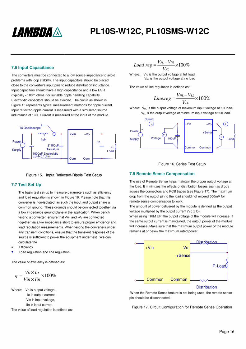
7.6 Input Capacitance
The converters must be connected to a low source impedance to avoidproblems with loop stability. The input capacitors should be placedclose to the converter’s input pins to reduce distribution inductance.Input capacitors should have a high capacitance and a low ESR(typically <100m ohms) for suitable ripple handling capability.Electrolytic capacitors should be avoided. The circuit as shown inFigure 15 represents typical measurement methods for ripple current.Input reflected-ripple current is measured with a simulated sourceinductance of 1uH. Current is measured at the input of the module.
1000uF ElectrolyticESR<0.1ohm
2*100uFTantalum
L11uH
+Power
Supply
To Oscilloscope
+Vin
Com
+Vo
Com
C2
R1Load
Figure 15. Input Reflected-Ripple Test Setup
7.7 Test Set-Up
The basic test set-up to measure parameters such as efficiencyand load regulation is shown in Figure 16. Please note that thisconverter is non-isolated, as such the input and output share acommon ground. These grounds should be connected together viaa low impedance ground plane in the application. When benchtesting a converter, ensure that -Vin and -Vo are connectedtogether via a low impedance short to ensure proper efficiency andload regulation measurements. When testing the converters underany transient conditions, ensure that the transient response of thesource is sufficient to power the equipment under test. We cancalculate the
• Efficiency• Load regulation and line regulation.
The value of efficiency is defined as:
%100×××=
IinVinIoVo
Where: Vo is output voltage, Io is output current,Vin is input voltage,Iin is input current.
The value of load regulation is defined as:
%100. ×−=NL
NLFL
VVV
regLoad
Where: VFL is the output voltage at full loadVNL is the output voltage at no load
The value of line regulation is defined as:
%100. ×−=
LL
LLHL
VVV
regLine
Where: VHL is the output voltage of maximum input voltage at full load.VLL is the output voltage of minimum input voltage at full load.
+Vin
Common
100uF
+Power
Supply
A
V
CurrentMeter
VoltageMeter
+Vo
Common
+Sense
LoadV
A
Figure 16. Series Test Setup
7.8 Remote Sense Compensation
The use of Remote Sense helps maintain the proper output voltage atthe load. It minimizes the effects of distribution losses such as dropsacross the connectors and PCB traces (see Figure 17). The maximumdrop from the output pin to the load should not exceed 500mV forremote sense compensation to work.The amount of power delivered by the module is defined as the outputvoltage multiplied by the output current (Vo x Io).When using TRIM UP, the output voltage of the module will increase. Ifthe same output current is maintained, the output power of the modulewill increase. Make sure that the maximum output power of the moduleremains at or below the maximum rated power.
When the Remote Sense feature is not being used, the remote sensepin should be disconnected.
Figure 17. Circuit Configuration for Remote Sense Operation
+Vin
Common Common
+VoDistributionLosses
R-Load
+Sense
DistributionLosses

PL10S-W12C, PL10SMS-W12C
Page 17
7.9 Output Voltage Adjustment
The output Voltage of the converters can be adjusted over the range of0.7525 to 5.0V by adding an external resistor (shown as Rtrim) inFigure 18. When the Trim resistor is not connected the output voltagedefaults to 0.7525V
+Vi
Com Com
+Vo
R trim-up
R-LoadTrim
Figure 18. Trim-up Voltage SetupThe value of Rtrim-up defined as:
Where:Rtrim-up is the external resistor in ohms,Vo is the desired output voltage
To give an example of the above calculation, to set a voltage of 3.3Vdc,Rtrim is given by:
Rtrim-up = 3.122K ohms
For various output voltages, the resistance values are provided in Table3.
Vo,set (V) Rtrim (Kohm)0.7525 Open
1.2 22.461.5 13.051.8 9.0242.0 7.4172.5 5.0093.3 3.1225.0 1.472
Table 3 – Trim Resistor Values
7.10 Output Ripple and Noise Measurement
The test set-up for noise and ripple measurements is shown in Figure19. A coaxial cable with a 50 ohm termination was used to preventimpedance mismatches. The Output Ripple & Noise is measured with
1uf ceramic and 10uf tantalum. The location for measurement is 50mmto 75mm (2” to 3”) from the module.
Figure 19. Output Voltage Ripple and Noise Measurement Set-Up
7.11 Output Capacitance
Lambda’s converters provide a stable output with or without externalcapacitors. For good transient response, low ESR output capacitorsshould be located close to the load..The converters are designed to work with a load capacitance of up to8,000uF. It is recommended that any additional capacitance be typically1,000uF and have an ESR of <20mohm. This capacitor should beconnected close to the load.
7.12 PL10SMS Reflow Profile
An example of the SMS reflow profile is given in Figure 20.Equipment used: SMD HOT AIR REFLOW HD-350SARAlloy: AMQ-M293TA or NC-SMQ92 IND-82088 SN63
REFLOW PROFILE
0
40
80
120
160
200
240
0 30 60 90 120 150 180 210 240TIME (SECONDS)
TEM
PE
RA
TUR
E º
C
Figure 20 SMS Reflow Profile
)10007525.0
10500( −
−=
VoRtrim
)10007525.03.3
10500( −
−=− upRtrim
Vin
Com
10uF 1uF
+
Power
Supply
VoutO
100uFESR<0.1Ω
Load
Sco
peCopper Strips

PL10S-W12C, PL10SMS-W12C
Page 18
8. Mechanical
8.1 Outline Diagrams
Dimensions are in millimeters and inchesTolerance: x.xx ±0.02 in. (0.5mm) , x.xxx ±0.010 in. (0.25 mm) unlessotherwise noted
A ll D im e n s io n s in In c h e s (m m )To le ra n c e :
.X X = ¡Ó0 .0 2 ( .X = ¡Ó0 .5 ) .X X X = ¡Ó0 .0 1 0 ( .X X = ¡Ó0 .2 5 )
L A Y O U T P A T TE R NT O P V IE W
0 .3 3 (8 .4 )0 .2 9 (7 .4 )
1 .1 m m P L A TE D T H R O U G H H O L E1 .6 m m P A D S IZ E
0 .0 2 5 (0 .6 4 )
0 .9 0 0 (2 2 .9 0 )
2 .0 0 (5 0 .8 )
54321
0 .1 4 (3 .6 )
0 .1 0 0 (2 .5 4 )
0 .4 0 0 (1 0 .2 0 )
P L 1 0 S
0 .5 1 0 (1 2 .9 5 )
1 21 11 0987
0 .0 5 0 (1 .3 0 )
0 .0 1 0 (0 .2 5 )m in .
0 .2 8 (7 .1 )
0 .0 2 5 (0 .6 4 )
0 .2 3 (5 .8 )
0 .3 2 7 (8 .3 0 )m a x.
6
P IN C O N N E C T IO NF U N C T IO N+ O u tp u t+ O u tp u t
+ S e n se+ O u tp u t
C o m m o nN o P in / P G o o d
P in
1234
56
7
891 01 1
C o m m o n+ V In p u t
+ V In p u tS e q u e n c in g
T r im
0 .0 2 5 (0 .6 4 )
0 .3 2 7 (8 .3 0 )m a x.
1 2 O n /O ff C o n tro l
Figure 21 PL10S-W12C Mechanical Outline Diagram
0.405 0.530
0.048
0.297
0.190.190.19
0.121.30
0.075
0.063
0.112
(33.0)(3.05)
(4.83) (4.83) (4.83)
(7.54)
(10.29) (13.46)
(1.91)
(1.22)(2.84)
(1.60)
+SENSETRIM+VOCOM
ON/OFF+VIN
0.065
0.346(8.80)
(1.65)
max.
Dimensions are in Inches(millimeters)
Tolerances :X.XX¡ Ó0.02in(0.5mm),X.XXX¡ Ó0.010in(0.25mm),unless otherwise noted.
BOTTOM VIEW OF BOARD
SURFACE MOUNT CONTACT
L1 INDUCTOR
SEQ PGood
0.19
(4.83)
0.19
(4.83)
(Option)
Figure 22 PL10SMS-W12C Mechanical Outline Diagram
8.2 SMS Tape and Reel Dimensions
The Tape Reel dimensions for the SMS module are shown in Figure 23.
E
F
W
PD t
Bo
AoKo
PoP2
WAo
Bo
KoP
FED
D1Po
P2t
Figure 23 – SMS Tape and Reel Dimensions


![Features...1,R 2, 3 = internal resistors [Ω] Rup Trim +Sense-Sense Trim Rdown Positve Logic DC-DC ON DC-DC OFF Open or 3.0VDC < V CTRL < 12VDC Short or 0VDC < V CTRL < 1…](https://img.pdfslide.us/doc/110x75/60c1f64ea1b3125bce622c56/features-1r-2-3-internal-resistors-rup-trim-sense-sense-trim-rdown.jpg)