Embed Size (px)
Citation preview

PIL APG-AED/10/5912Notification Date 09/23/2010
L4949E Lead-Free migration to Advanced uPPF frame
1/32
PRODUCT INFORMATIONLETTER®
PIL APG-AED/10/5912 - Notification Date 09/23/2010
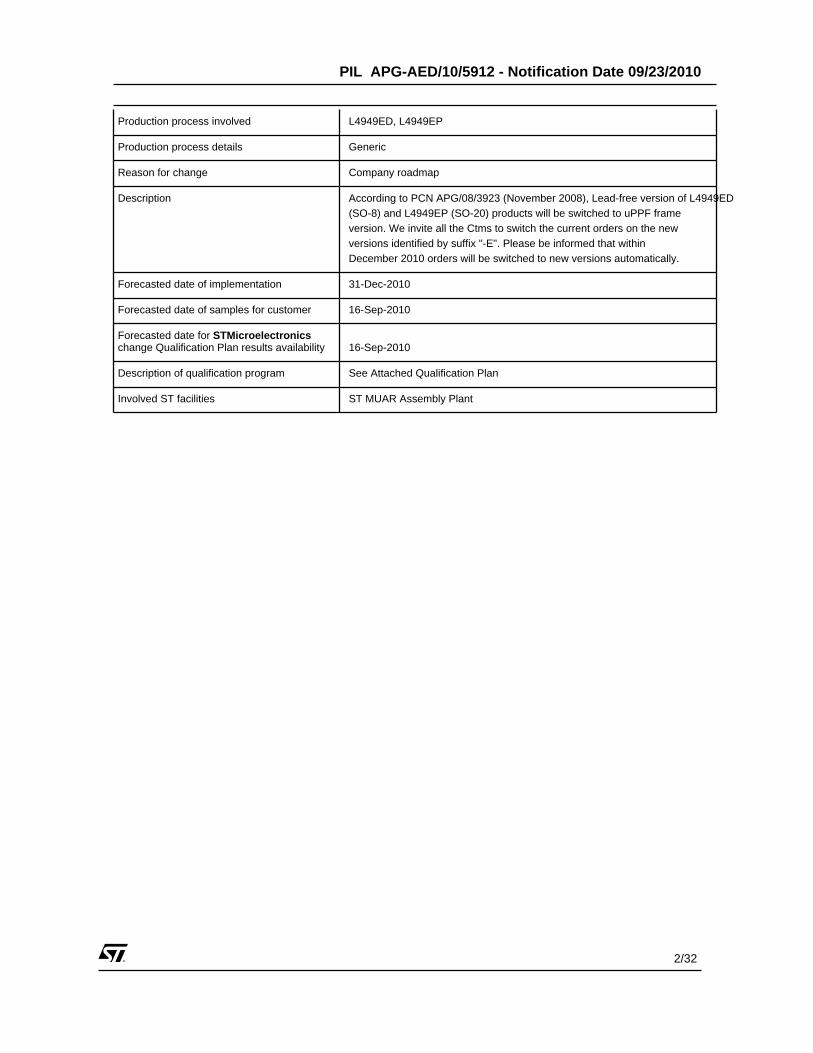
Production process involved L4949ED, L4949EP
Production process details Generic
Reason for change Company roadmap
Description According to PCN APG/08/3923 (November 2008), Lead-free version of L4949ED(SO-8) and L4949EP (SO-20) products will be switched to uPPF frameversion. We invite all the Ctms to switch the current orders on the newversions identified by suffix "-E". Please be informed that withinDecember 2010 orders will be switched to new versions automatically.
Forecasted date of implementation 31-Dec-2010
Forecasted date of samples for customer 16-Sep-2010
Forecasted date for STMicroelectronicschange Qualification Plan results availability 16-Sep-2010
Description of qualification program See Attached Qualification Plan
Involved ST facilities ST MUAR Assembly Plant
® 2/32
PIL APG-AED/10/5912 - Notification Date 09/23/2010
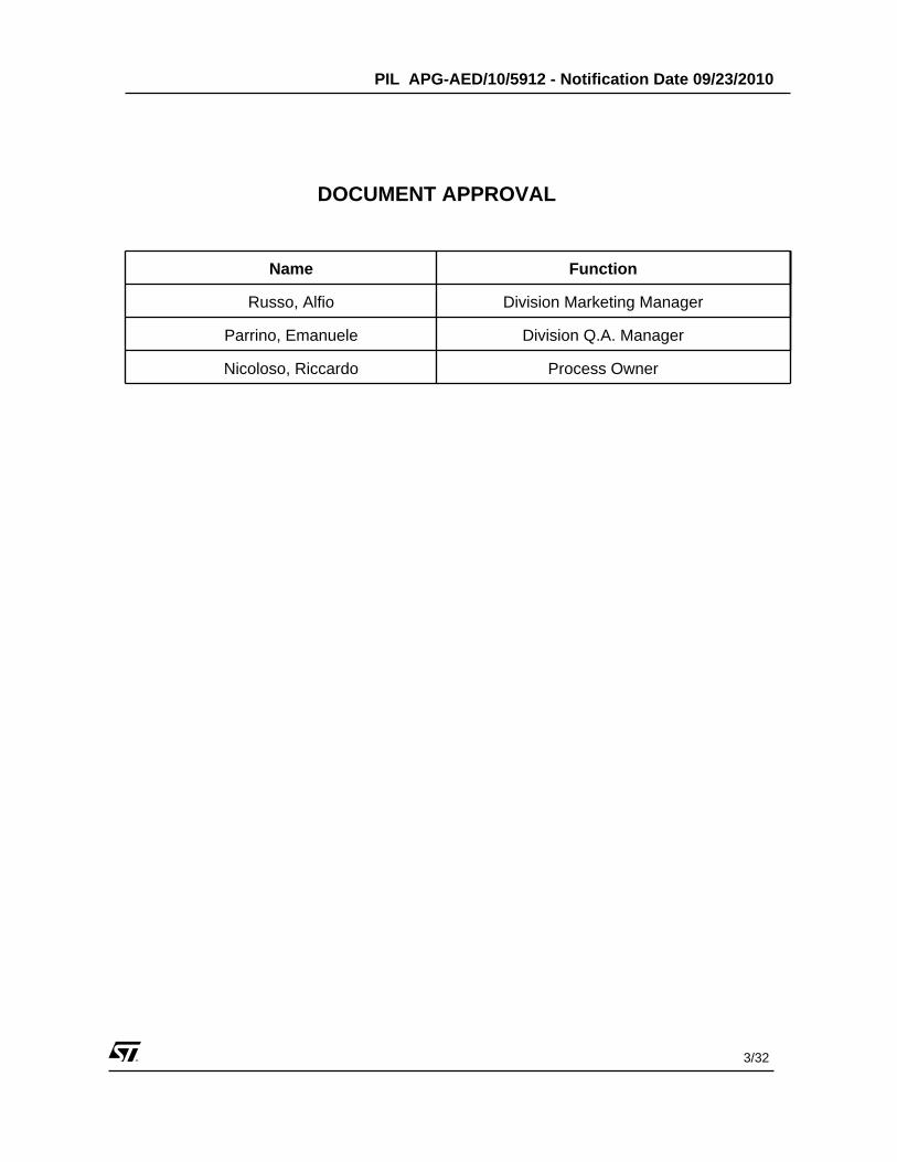
DOCUMENT APPROVAL
Name Function
Russo, Alfio Division Marketing Manager
Parrino, Emanuele Division Q.A. Manager
Nicoloso, Riccardo Process Owner
® 3/32

Product Information Letter L4949E lead-free migration to Advanced uPPF frame Dear Customer,
According to the PCN APG/08/3923 (notification date: 11/06/2008), STMicroelectronics improved lead‐free production of L4949ED (SO‐8) and L4949EP (SO‐20) introducing advanced uPPF frame.
Today the majority of ST production is already using the new frame option (linked to a dedicated commercial product having the suffix “‐E”).
With the aim to improve product quality and reliability, we invite you all to switch the current orders on the new L4949E lead‐free option. The below table, reporting the old and new commercial, is a helpful guide for correct order insertion:
OLD FRAME Commercial Product
NEW ADVENCED uPPF Commercial Product
L4949ED L4949ED‐EL4949ED013TR L4949EDTR‐E L4949EP L4949EP‐E L4949EP013TR L4949EPTR‐E
We take the chance to inform you that in December 2010 the lead‐free orders on older
commercial product (without the suffix “‐E”) will be switched on the newer Commercial Product (suffix "-E”) linked to the advanced uPPF frame. Of course, the migration will not impact the order confirmation date. STMicroelectronics Date Automotive Product Group September 15th, 2010
The ST logo is a registered trademark of STMicroelectronics © 2002 STMicroelectronics - All Rights Reserved.
STMicroelectronics GROUP OF COMPANIES
Australia - Brazil - Canada - China - France - Germany - Italy - Japan - Korea - Malaysia - Malta - Mexico – Morocco -
The Netherlands - Singapore - Spain - Sweden - Switzerland - Taiwan - Thailand - United Kingdom - U.S.A.

Advanced uPPF and standard PPF frame Comparison
See below layers structures and comparison between standard PPF and uPPF frames . Reliability evaluation on tet vehicles follows.
Corporate Packaging & Automation
June, 21st 06
Ni (20 ~50):40
Pd (1.2~ 4.5):2.0
Au Flash (0.12 ~0.45):0.2
Base Material(Cu only)
Conventional Au flash PPFµ-PPF
advanced
Ni : 20 µ’’
Pd : 0.5 µ’’Au-Ag : 0.8 µ’’
Base Material
Unit : µ” ( 1µ” = 0.025 µm)
Layer Structure Layers Structure

APG/CPG BACK-END Q&R Page 1 of 12
ER000409AG6053 February 19th, 2009 Author: D. CASIRAGHI
ADVANCED µµµµ-PPF FOR Pb-FREE SOIC NARROW, MUAR
RELIABILITY EVALUATION REPORT TEST VEHICLE: W023
Abstract
Aim of the present reliability exercise was to assess the “Advanced Micro-PPF” lead-frame proposed for Pb-free SO-Narrow package in order to increase molding compound adhesion and solderability. The new glue ABLEBOND 8601S-25, replacement of Hitachi EN4900ST10 for workability improvement, has been evaluated too.
Conclusion
On the basis of the results summarized and documented within the present report, the adoption of “Advanced µ-PPF” strongly improves the robustness margin of Pb-free SOIC-Narrow package against thermal fatigue. The new glue ABLEBOND 8601S-25 does not introduce significant variations in the expected reliability performance of the package.
The reliability stress matrix on this test-vehicle has been optimized taking into account the available results on other products, in order to achieve a full AEC-Q100-compliant data collection for the proposed change.

APG/CPG BACK-END Q&R Page 2 of 12
ER000409AG6053 February 19th, 2009 Author: D. CASIRAGHI
Reliability test conditions and results
TEST NAME
CONDITIONS [SPEC] U537 REJ./S.S.
NOTES
JL3 24h bake @ 125°C 192h @ 30°C / 60% RH
reflow simulation (3 times) at TMAX=260°C [IPC/Jedec J-STD-020C]
0/200 1
JL3 + TCT Ta=-65/+150°C, 1000 cycles 0/77 1, 2, 3
JL3+THB Ta=85°C, RH=85%, 1000h Vs=16V Pd=negligible
0/77 -
NOTES:
Construction note
Technical code : J5O7*W023FAW
Diffusion process : BIP Wafer diameter : 5
Diffusion site : AMK 5
Die size (mm2) : 2160x1960 Metal levels : 2,AlSi/AlSiCu Passivation : SiN+Polyimide
Back finishing : CHROMIUM/NICKEL
Package name : SO 08 .15 JEDEC
Assembly site : MUAR Leadframe : SO 8L 94x125 Du Flo OpC uAdvPPF
Die attach : ABLEBOND 8601S-25 Wire bonding : Au 1mils
Molding compound : NITTO MP8000CH4-2A
Lead finishing : Ni/Pd/Au Lot _id : 90830
Attachments
1) Reliability tests description 2) List of stress equipment 3) Physical analysis report 4) Reflow profile
1 SAM analysis after JL3 preconditioning shows no significant delamination at the die-molding compound, lead tips and through the die-attach layer. Detail in attachment n. 3.
2 Wire bonding strength after the stress has been successfully verified through wire-pull test and ball shear test: neither abnormal break loads, nor forbidden failure modes have been detected. Detail in attachment n. 3.
3 Visual and SEM inspection after the stress test have pointed out no remarkable degradation of silicon passivation, metal interconnects and wire bonds. Detail in attachment n. 3.
APG/CPG BACK-END Q&R Page 3 of 12
ER000409AG6053 February 19th, 2009 Author: D. CASIRAGHI
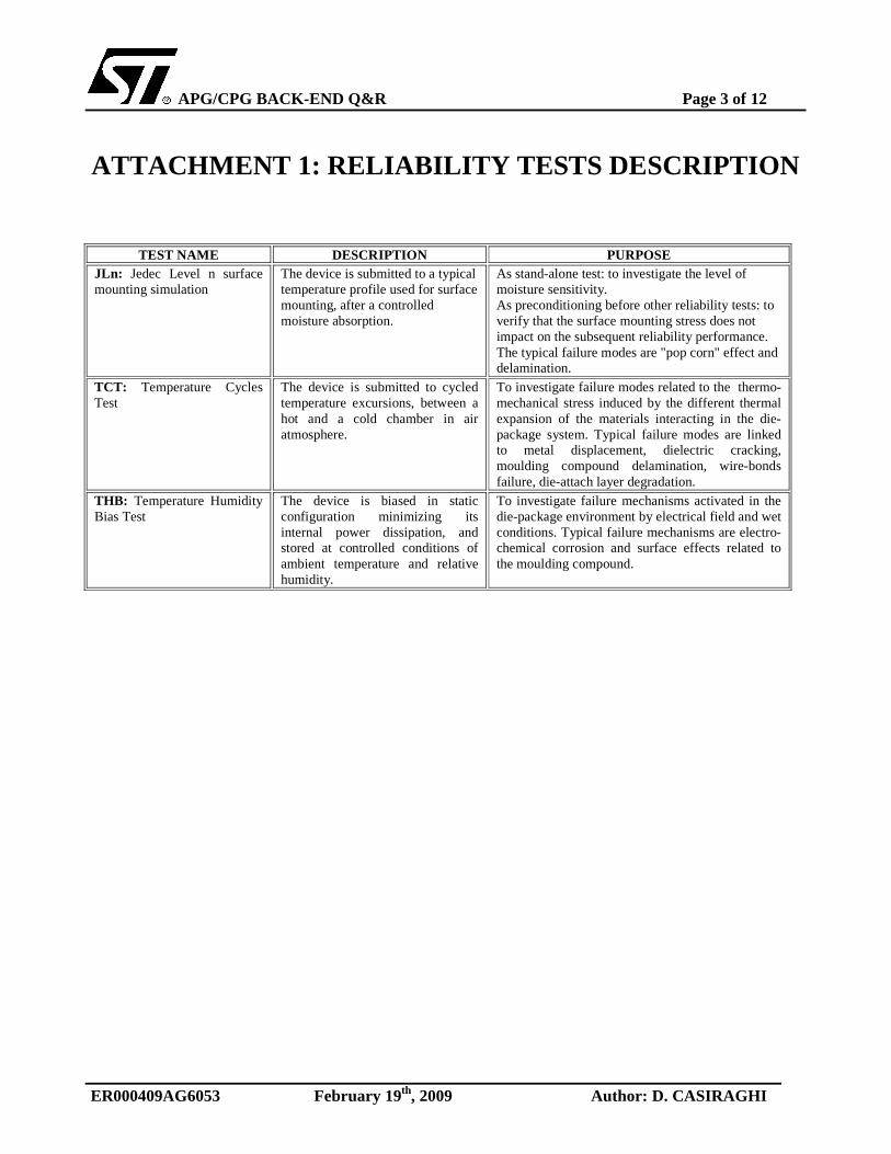
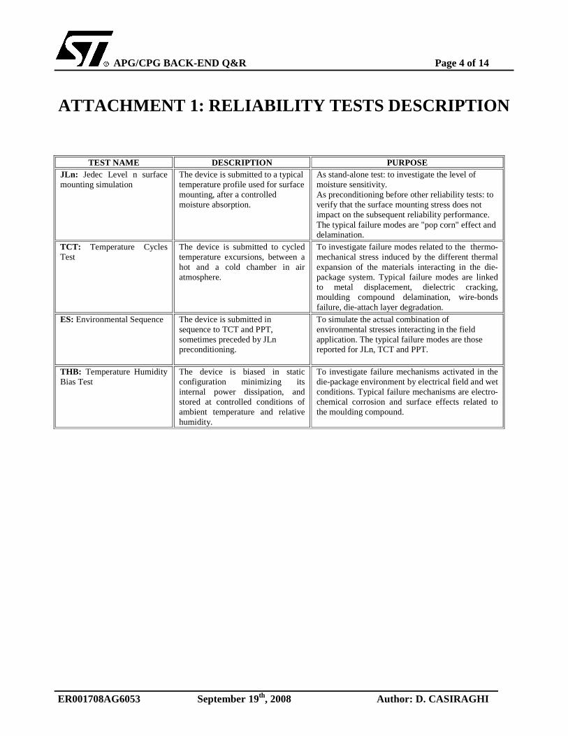
ATTACHMENT 1: RELIABILITY TESTS DESCRIPTION
TEST NAME DESCRIPTION PURPOSE JLn: Jedec Level n surface mounting simulation
The device is submitted to a typical temperature profile used for surface mounting, after a controlled moisture absorption.
As stand-alone test: to investigate the level of moisture sensitivity. As preconditioning before other reliability tests: to verify that the surface mounting stress does not impact on the subsequent reliability performance. The typical failure modes are "pop corn" effect and delamination.
TCT: Temperature Cycles Test
The device is submitted to cycled temperature excursions, between a hot and a cold chamber in air atmosphere.
To investigate failure modes related to the thermo-mechanical stress induced by the different thermal expansion of the materials interacting in the die-package system. Typical failure modes are linked to metal displacement, dielectric cracking, moulding compound delamination, wire-bonds failure, die-attach layer degradation.
THB: Temperature Humidity Bias Test
The device is biased in static configuration minimizing its internal power dissipation, and stored at controlled conditions of ambient temperature and relative humidity.
To investigate failure mechanisms activated in the die-package environment by electrical field and wet conditions. Typical failure mechanisms are electro-chemical corrosion and surface effects related to the moulding compound.

APG/CPG BACK-END Q&R Page 4 of 12
ER000409AG6053 February 19th, 2009 Author: D. CASIRAGHI
ATTACHMENT 2: LIST OF STRESS EQUIPMENT
EQUIPMENT TYPE / LOCATION USED FOR…MAZZALI THRMAIR STATIC OVEN / STM Agrate JL3 (dry bake step)
MAZZALI CLIMATEST CLIMATIC CHAMBER /STM Agrate JL3 (moisture soak step) HERAEUS NOBLELIGHT REFLOW FURNACE (7 zones) / STM Agrate JL3 (reflow simulation step)
WEISS TS130 AIR TO AIR SHOCK (2 chambers) / STM Muar TC 1000
MAZZALI CLIMATEST CLIMATIC CHAMBER/ STM Agrate THB 1000h

APG/CPG BACK-END Q&R Page 5 of 12
ER000409AG6053 February 19th, 2009 Author: D. CASIRAGHI
ATTACHMENT 3: PHYSICAL ANALYSIS REPORT
Technical code : J5O7*W023FAW
Package : SO-8N
Lot_id : 90830
Evaluation subject : SO-8 N advanced µPPF leadframe + new glue
Author : D. Casiraghi
Analysis status: RUNNING X COMPLETED
ANALYSIS PROGRAM
DESTRUCTIVE ITEMS NON DESTRUCTIVE ITEMS WHEN
Wire pull test Ball Shear test Internal visual SEM inspection SAM inspection Other
X JL3@260°C X X X X X JL3+1000TC
RESULTS SUMMARY
• SAM analysis after JL3 and TC shows no significant delamination at the die-molding compound, lead tips and through the die-attach layer. Uncritical delamination at the die-pad top surface has been observed (no down-bonding present).
• Visual and SEM inspection after JL3+TC showed no significant passivation cracks and no concern in terms of metal and wire bond integrity.
• Wire bonding strength after TC stress has been successfully verified through wire-pull and ball shear tests: neither abnormal break loads, nor forbidden failure modes have been found.

APG/CPG BACK-END Q&R Page 6 of 12
ER000409AG6053 February 19th, 2009 Author: D. CASIRAGHI
TECHNICAL CODE PACKAGE ANALYSIS ITEM STRESS TEST
J5O7*W023FAW SO-8 N SAM inspection JL3@260°C
TEST EQUIPMENT: SONOSCAN D9000 (Scanning Acoustic Microscope)
C-SAM typical case with waveform
T-SAM typical case C-SAM typical case (bottom view)
Defective parts (delamination)Lot Sample sizedie-mold (C-scan) die-attach (T-scan) l/f-mold (C-scan) diepad-mold (C-scan)
90830 20 0/20 0/20 0/20 0/20 Transducer frequency (MHz) 30 30 30 30

APG/CPG BACK-END Q&R Page 7 of 12
ER000409AG6053 February 19th, 2009 Author: D. CASIRAGHI
TECHNICAL CODE PACKAGE ANALYSIS ITEM STRESS TEST
J5O7*W023FAW SO-8 N SAM inspection JL3 + 1000TC (-65/+150°C)
TEST EQUIPMENT: SONOSCAN D9000 (Scanning Acoustic Microscope)
C-SAM typical case with waveform
T-SAM typical case C-SAM typical case (bottom view)
Defective parts (delamination)Lot Sample sizedie-mold (C-scan) die-attach (T-scan) l/f-mold (C-scan) diepad-mold top(C-scan)
90830 20 0/20 0/20 0/20 20/20* Transducer frequency (MHz) 30 30 30 30
* uncritical delamination due to absence of wire-bonds on the die-pad.

APG/CPG BACK-END Q&R Page 8 of 12
ER000409AG6053 February 19th, 2009 Author: D. CASIRAGHI
TECHNICAL CODE PACKAGE LOT ANALYSIS ITEM
J5O7*W023FAW SO-8 N 90830 Internal visual
ANALYSIS SUMMARY:
WHAT WHEN SAMPLE SIZE /LOT RESULT
Passivation and metal integrity JL3+1000 TC 5pcs/1 No passivation-cracks / no metal displacement (photo 1-4)
DOCUMENTATION:
Photo 1 (20X) Photo 2 (50X)
Photo 3 (50X) Photo 4 (50X)
TEST EQUIPMENT: LEICA (Optical Microscope)

APG/CPG BACK-END Q&R Page 9 of 12
ER000409AG6053 February 19th, 2009 Author: D. CASIRAGHI
TECHNICAL CODE PACKAGE LOT ANALYSIS ITEM
J5O7*W023FAW SO-8 N 90830 SEM inspection
ANALYSIS SUMMARY:
WHAT WHEN SAMPLE RESULT
Stitch-bond on leads / ball bond JL3+1000TC 5pcs No visible defect (photo 1-6)
DOCUMENTATION:
Photo 1 Photo 2 Photo 3
Photo 4 Photo 5 Photo 6
TEST EQUIPMENT: HITACHI (Scanning Electron Microscope)
APG/CPG BACK-END Q&R Page 10 of 12
ER000409AG6053 February 19th, 2009 Author: D. CASIRAGHI
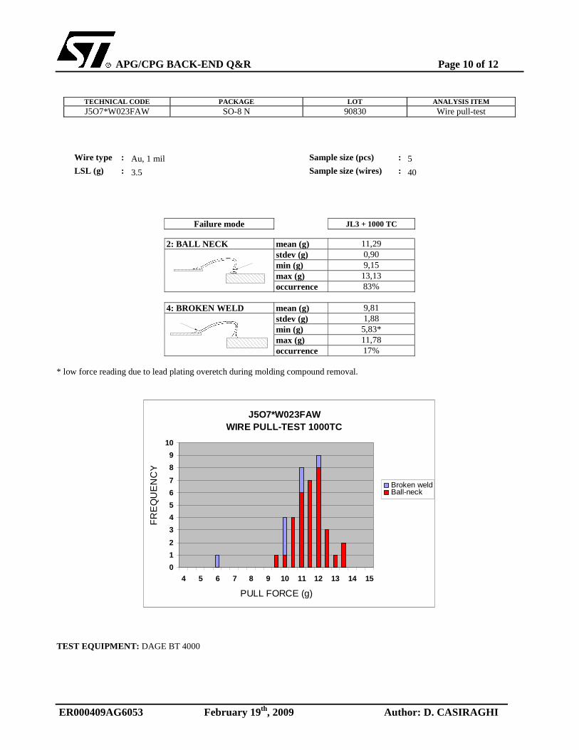
TECHNICAL CODE PACKAGE LOT ANALYSIS ITEM J5O7*W023FAW SO-8 N 90830 Wire pull-test
Wire type : Au, 1 mil Sample size (pcs) : 5 LSL (g) : 3.5 Sample size (wires) : 40
Failure mode JL3 + 1000 TC
2: BALL NECK mean (g) 11,29 stdev (g) 0,90 min (g) 9,15 max (g) 13,13 occurrence 83%
4: BROKEN WELD mean (g) 9,81 stdev (g) 1,88 min (g) 5,83* max (g) 11,78 occurrence 17%
* low force reading due to lead plating overetch during molding compound removal.
J5O7*W023FAWWIRE PULL-TEST 1000TC
0
1
2
3
4
5
6
7
8
9
10
151413121110987654
PULL FORCE (g)
FR
EQ
UE
NC
Y
Broken weldBall-neck
TEST EQUIPMENT: DAGE BT 4000
APG/CPG BACK-END Q&R Page 11 of 12
ER000409AG6053 February 19th, 2009 Author: D. CASIRAGHI
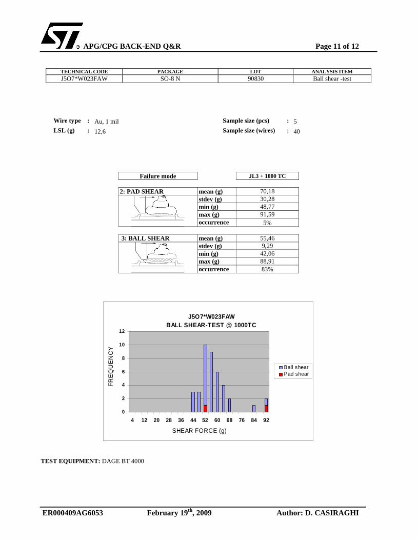
TECHNICAL CODE PACKAGE LOT ANALYSIS ITEM J5O7*W023FAW SO-8 N 90830 Ball shear -test
Wire type : Au, 1 mil Sample size (pcs) : 5
LSL (g) : 12,6 Sample size (wires) : 40
Failure mode JL3 + 1000 TC
2: PAD SHEAR mean (g) 70,18 stdev (g) 30,28 min (g) 48,77 max (g) 91,59 occurrence 5%
3: BALL SHEAR mean (g) 55,46
stdev (g) 9,29 min (g) 42,06 max (g) 88,91 occurrence 83%
J5O7*W023FAWBALL SHEAR-TEST @ 1000TC
0
2
4
6
8
10
12
92847668605244362820124
SHEAR FORCE (g)
FR
EQ
UE
NC
Y
Ball shearPad shear
TEST EQUIPMENT: DAGE BT 4000
APG/CPG BACK-END Q&R Page 12 of 12
ER000409AG6053 February 19th, 2009 Author: D. CASIRAGHI
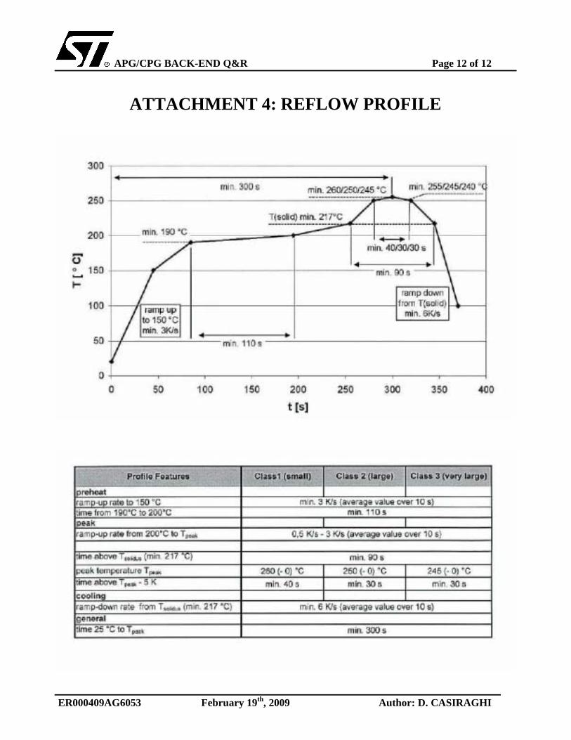
ATTACHMENT 4: REFLOW PROFILE

APG/CPG BACK-END Q&R Page 1 of 14
ER001708AG6053 September 19th, 2008 Author: D. CASIRAGHI
ADVANCED µµµµ-PPF FOR Pb-FREE SOIC WIDE, MUAR
RELIABILITY EVALUATION REPORT TEST VEHICLE: U447
Abstract
Aim of the present reliability exercise was to assess the “Advanced Micro-PPF” lead-frame proposed for Pb-free SO-Wide package in order to improve molding compound adhesion and solderability. The U447 has been selected to verify the integrity of GND down-bonding, performed on a dedicated lead-frame design with anchorage slots on the die-pad.
Conclusion
On the basis of the results summarized and documented within the present report, the adoption of “Advanced µ-PPF” strongly improves the robustness margin of Pb-free SOIC-Wide package against thermal fatigue, also preserving the integrity of GND down-bonds.
The reliability stress matrix has been successfully enlarged with wet environmental tests (ES and THB) in order to exclude any potential drawback in the new lead-frame implementation and contribute to a full AEC-Q100-compliant data collection for the proposed change (other SOIC-Wide test-vehicle have been tested in this perspective).
Released by: ALBERTO MANCALEONI
APG Back-end Q&R – Reliability Manager

APG/CPG BACK-END Q&R Page 2 of 14
ER001708AG6053 September 19th, 2008 Author: D. CASIRAGHI
Reliability test conditions and results
TEST NAME
CONDITIONS [SPEC] U447 REJ./S.S.
NOTES
JL3 24h bake @ 125°C 192h @ 30°C / 60% RH
reflow simulation (3 times) at TMAX=260°C [IPC/Jedec J-STD-020C]
0/291 1, 5
JL3 + TCT Ta=-50/+150°C, 1000 cycles 0/77 2, 3, 4
JL3+ES 100 TC (-50/+150°C) + 96h PPT (2atm, 121°C)
0/77 2, 3
JL3+THB Ta=85°C, RH=85%, 1000h V1=45V ; PD negligible
0/87 -
NOTES: 1 SAM analysis after preconditioning shows no significant delamination at the die-molding compound, lead tips,
die-pad interfaces and through the die-attach layer. Detail in attachment n. 3. 2 Wire bonding strength after the stress has been successfully verified through wire-pull test and ball shear test:
neither abnormal break loads, nor forbidden failure modes have been detected. Detail in attachment n. 3. 3 Visual and SEM inspection after the stress test have pointed out no remarkable degradation of silicon passivation
and metal interconnects. Stitch bonds integrity on internal lead-tips and die-pad has been carefully checked after TC. Detail in attachment n. 3.
4 SAM analysis after TC shows no significant delamination at the die-molding compound and lead tips interfaces; minor delaminations at the die-pad interfaces and through the die-attach layer have been observed on very limited areas. Detail in attachment n. 3.
5 Reflow profile according to Bosch specification (see attachment #4) performed in Reutlingen.

APG/CPG BACK-END Q&R Page 3 of 14
ER001708AG6053 September 19th, 2008 Author: D. CASIRAGHI
Construction note
Technical code : J6Z7*U447CA6
Diffusion process : BCD3 Wafer diameter : 6”
Diffusion site : ANG-MO-KIO
Die size (mm2) : 4.12x2.51 Metal levels : 2, Al/Si/Cu Passivation : USG-PSG-SiON-PIX
Back finishing : Lapped Silicon
Package name : SO-20L
Assembly site : MUAR Leadframe : SO 20L 195x250 MtBtw16+2+2 uAdvPPF
Die attach : HITACHI EN4900 ST12 Wire bonding : Au, 1.5 mils
Molding compound : SUMITOMO EME7026
Lead finishing : Ni/Pd/Au PPF Lot _id : 99804
Attachments
1) Reliability tests description 2) List of stress equipment 3) Physical analysis report 4) Reflow profile
APG/CPG BACK-END Q&R Page 4 of 14
ER001708AG6053 September 19th, 2008 Author: D. CASIRAGHI
ATTACHMENT 1: RELIABILITY TESTS DESCRIPTION
TEST NAME DESCRIPTION PURPOSE JLn: Jedec Level n surface mounting simulation
The device is submitted to a typical temperature profile used for surface mounting, after a controlled moisture absorption.
As stand-alone test: to investigate the level of moisture sensitivity. As preconditioning before other reliability tests: to verify that the surface mounting stress does not impact on the subsequent reliability performance. The typical failure modes are "pop corn" effect and delamination.
TCT: Temperature Cycles Test
The device is submitted to cycled temperature excursions, between a hot and a cold chamber in air atmosphere.
To investigate failure modes related to the thermo-mechanical stress induced by the different thermal expansion of the materials interacting in the die-package system. Typical failure modes are linked to metal displacement, dielectric cracking, moulding compound delamination, wire-bonds failure, die-attach layer degradation.
ES: Environmental Sequence The device is submitted in sequence to TCT and PPT, sometimes preceded by JLn preconditioning.
To simulate the actual combination of environmental stresses interacting in the field application. The typical failure modes are those reported for JLn, TCT and PPT.
THB: Temperature Humidity Bias Test
The device is biased in static configuration minimizing its internal power dissipation, and stored at controlled conditions of ambient temperature and relative humidity.
To investigate failure mechanisms activated in the die-package environment by electrical field and wet conditions. Typical failure mechanisms are electro-chemical corrosion and surface effects related to the moulding compound.

APG/CPG BACK-END Q&R Page 5 of 14
ER001708AG6053 September 19th, 2008 Author: D. CASIRAGHI
ATTACHMENT 2: LIST OF STRESS EQUIPMENT
EQUIPMENT TYPE / LOCATION USED FOR…BINDER FE115 STATIC OVEN / RB Reutlingen JL3 (dry bake step)
CTS C+10/200 CLIMATIC CHAMBER / RB Reutlingen JL3 (moisture soak step) REHM V8 REFLOW FURNACE / RB Reutlingen JL3 (reflow simulation step)
WEISS TS130 AIR TO AIR SHOCK (2 chambers) / STM Muar TC, ES (100 TC step)
MAZZALI CLIMATEST CLIMATIC CHAMBER/ STM Agrate THB
MAZZALI PRESSURE POT/ STM Muar ES (96h PPT step)

APG/CPG BACK-END Q&R Page 6 of 14
ER001708AG6053 September 19th, 2008 Author: D. CASIRAGHI
ATTACHMENT 3: PHYSICAL ANALYSIS REPORT
Technical code : J6Z7*U447CA6
Package : SO-20L
Lot_id : 99804
Evaluation subject : SO-20L advanced µPPF Leadframe
Author : D. Casiraghi
Analysis status: RUNNING X COMPLETED
ANALYSIS PROGRAM
DESTRUCTIVE ITEMS NON DESTRUCTIVE ITEMS WHEN
Wire pull test Ball Shear test Internal visual SEM inspection SAM inspection Other
X JL3@260°C X X X X X JL3+1000TC X X JL3+ES (100TC+96hAC)
RESULTS SUMMARY
• SAM analysis after JL3 preconditioning shows no significant delamination at the die-molding compound, lead tips, die-pad interfaces and through the die-attach layer.
• SAM analysis after TC shows no significant delamination at the die-molding compound and lead tips interfaces; minor delaminations at the die-pad interfaces and through the die-attach layer have been observed on very limited areas.
• Visual and SEM inspection after JL3+TC showed minor and physiological passivation cracks and no concern in terms of metal and wire bond integrity.
• Visual inspection after ES stress test did not show any remarkable defect in terms of metal corrosion and oxidation.
• Wire bonding strength after TC and ES stress has been successfully verified through wire-pull test and ball shear test: neither abnormal break loads, nor forbidden failure modes have been found. With particular focus on 2nd bond (main reason for advanced µPPF adoption) no degradation trend has been observed until 1000 cycles on both standard bonds and down-bonds.

APG/CPG BACK-END Q&R Page 7 of 14
ER001708AG6053 September 19th, 2008 Author: D. CASIRAGHI
TECHNICAL CODE PACKAGE ANALYSIS ITEM STRESS TEST
J6Z7*U447CA6 SO 20 SAM inspection JL3@260°C
TEST EQUIPMENT: SONOSCAN D9000 (Scanning Acoustic Microscope)
C-SAM typical case with waveform
T-SAM typical case C-SAM typical case (bottom view)
Defective parts (delamination)Lot Sample sizedie-mold (C-scan) die-attach (T-scan) l/f-mold (C-scan) diepad-mold (C-scan)
99804 20 0/20 0/20 0/20 0/20 Transducer frequency (MHz) 30 30 30 30

APG/CPG BACK-END Q&R Page 8 of 14
ER001708AG6053 September 19th, 2008 Author: D. CASIRAGHI
TECHNICAL CODE PACKAGE ANALYSIS ITEM STRESS TEST
J6Z7*U447CA6 SO 20 SAM inspection JL3@260°C + 1000TC (-50/+150°C)
TEST EQUIPMENT: SONOSCAN D9000 (Scanning Acoustic Microscope)
C-SAM typical case with waveform
T-SAM typical case C-SAM typical case (bottom view)
Defective parts (delamination)Lot Sample sizedie-mold (C-scan) die-attach (T-scan) l/f-mold (C-scan) diepad-mold (C-scan)
99804 20 0/20 0/20* 0/20* 0/20 Transducer frequency (MHz) 30 30 30 30
*minor delamination on top side (batwing leads) , and die-attach perimeter.
APG/CPG BACK-END Q&R Page 9 of 14
ER001708AG6053 September 19th, 2008 Author: D. CASIRAGHI
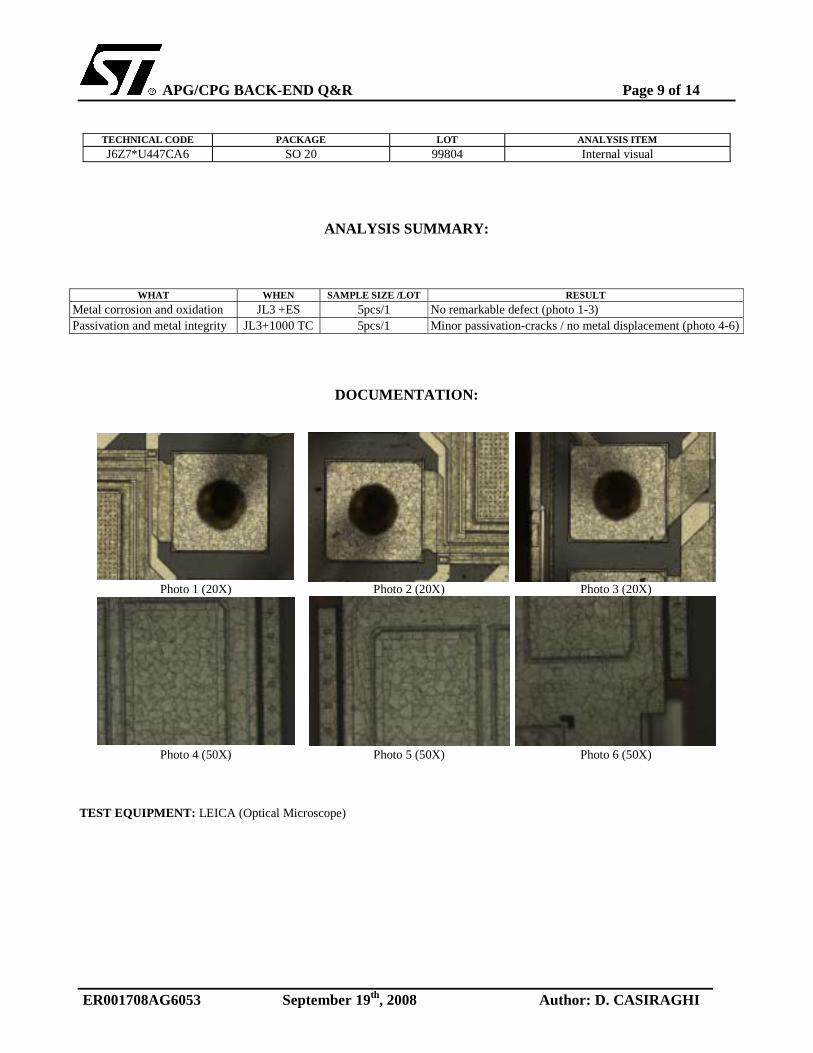
TECHNICAL CODE PACKAGE LOT ANALYSIS ITEM
J6Z7*U447CA6 SO 20 99804 Internal visual
ANALYSIS SUMMARY:
WHAT WHEN SAMPLE SIZE /LOT RESULT
Metal corrosion and oxidation JL3 +ES 5pcs/1 No remarkable defect (photo 1-3) Passivation and metal integrity JL3+1000 TC 5pcs/1 Minor passivation-cracks / no metal displacement (photo 4-6)
DOCUMENTATION:
Photo 1 (20X) Photo 2 (20X) Photo 3 (20X)
Photo 4 (50X) Photo 5 (50X) Photo 6 (50X)
TEST EQUIPMENT: LEICA (Optical Microscope)
APG/CPG BACK-END Q&R Page 10 of 14
ER001708AG6053 September 19th, 2008 Author: D. CASIRAGHI
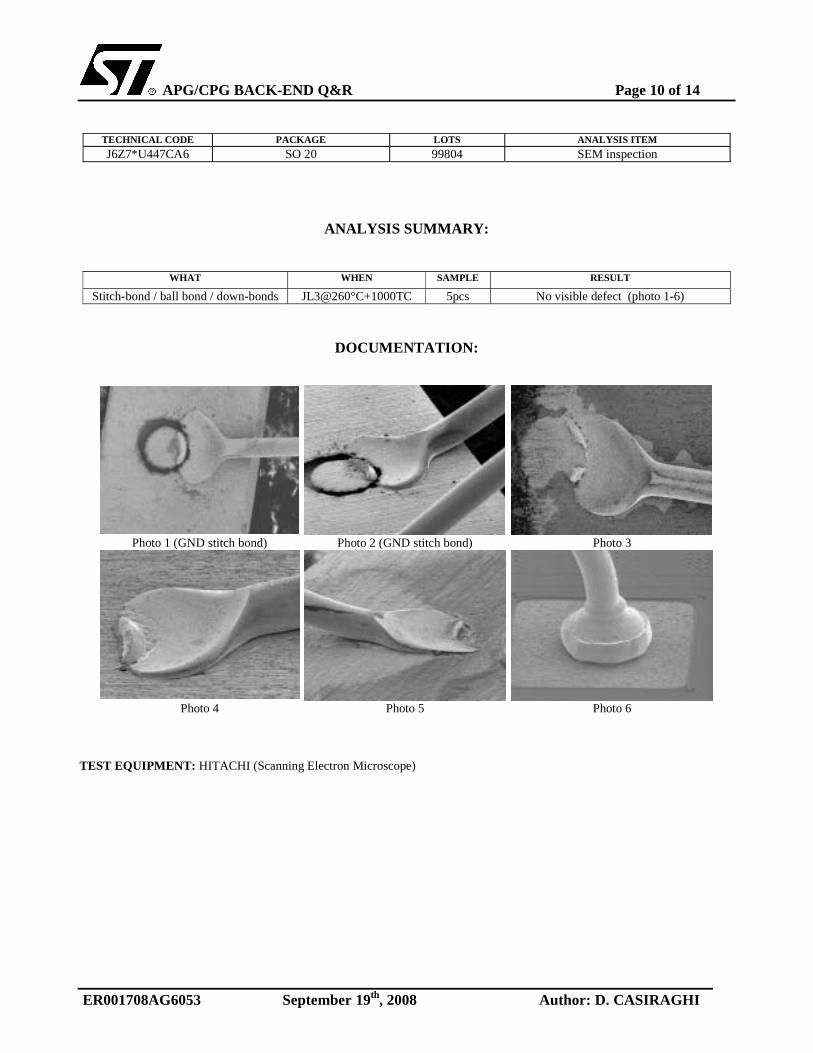
TECHNICAL CODE PACKAGE LOTS ANALYSIS ITEM
J6Z7*U447CA6 SO 20 99804 SEM inspection
ANALYSIS SUMMARY:
WHAT WHEN SAMPLE RESULT
Stitch-bond / ball bond / down-bonds JL3@260°C+1000TC 5pcs No visible defect (photo 1-6)
DOCUMENTATION:
Photo 1 (GND stitch bond) Photo 2 (GND stitch bond) Photo 3
Photo 4 Photo 5 Photo 6
TEST EQUIPMENT: HITACHI (Scanning Electron Microscope)

APG/CPG BACK-END Q&R Page 11 of 14
ER001708AG6053 September 19th, 2008 Author: D. CASIRAGHI
BONDING DIAGRAM
Bonding diagram
U447 wires submitted to pull and ball shear test

APG/CPG BACK-END Q&R Page 12 of 14
ER001708AG6053 September 19th, 2008 Author: D. CASIRAGHI
TECHNICAL CODE PACKAGE LOT ANALYSIS ITEM J6Z7*U447CA6 SO-20L 99804 Wire pull-test
Wire type : Au, 1,5 mil Sample size (pcs) : 5 LSL (g) : 7.5 Sample size (wires) : 60
Failure mode JL3 + 1000 TC JL3 + ES
2: BALL NECK mean (g) 19.68 18.72 stdev (g) 2.18 2.54 min (g) 14.80 13.63 max (g) 24.03 23.52 occurrence 92% 93%
3: LOOP CENTRE mean (g) 21.55 22.09
stdev (g) 1.04 0.46 min (g) 20.44 21.58 max (g) 22.89 22.49 occurrence 8% 7%
J6Z7*U447CA6WIRE PULL-TEST @ 1000TC
0
2
4
6
8
10
12
14
30282624222018161412108
PULL FORCE (g)
FR
EQ
UE
NC
Y
Loop-centre
Ball-neck
J6Z7*U447CA6WIRE PULL-TEST @ ES
0
1
2
3
4
5
6
7
8
9
10
30282624222018161412108
PULL FORCE (g)
FR
EQ
UE
NC
Y
Loop-centre
Ball-neck

APG/CPG BACK-END Q&R Page 13 of 14
ER001708AG6053 September 19th, 2008 Author: D. CASIRAGHI
TECHNICAL CODE PACKAGE LOT ANALYSIS ITEM J6Z7*U447CA6 SO 20 99804 Ball shear test
Wire type : Au, 1,5 mil Sample size (pcs) : 5
LSL (g) : 45 Sample size (wires) : 60
Failure mode JL3 + 1000 TC
2: PAD SHEAR mean (g) 92.88 stdev (g) 6.59 min (g) 87.33 max (g) 101.36 occurrence 7%
3: BALL SHEAR mean (g) 96.49 stdev (g) 4.22 min (g) 85.46 max (g) 105.66 occurrence 93%
J6Z7*U447CA6BALL SHEAR-TEST @ 1000TC
0
2
4
6
8
10
12
14
110106102989490868278747066
SHEAR FORCE (g)
FR
EQ
UE
NC
Y
Ball shear
Pad shear

APG/CPG BACK-END Q&R Page 14 of 14
ER001708AG6053 September 19th, 2008 Author: D. CASIRAGHI
ATTACHMENT 4: REFLOW PROFILE

PIL APG-AED/10/5912 - Notification Date 09/23/2010
Please Read Carefully:
Information in this document is provided solely in connection with ST products. STMicroelectronics NV and its subsidiaries(‘‘ST’’) reserve theright to make changes, corrections, modifications or improvements, to this document, and the products and services described herein at anytime, without notice.
All ST products are sold pursuant to ST’s terms and conditions of sale.
Purchasers are solely responsible for the choice, selection and use of the ST products and services described herein, and ST assumes noliability whatsoever relating to the choice, selection or use of the ST products and services described herein.
No license, express or implied, by estoppel or otherwise, to any intellectual property rights is granted under this document. If any part of thisdocument refers to any third party products or services it shall not be deemed a license grant by ST for the use of such third party productsor services, or any intellectual property contained therein or considered as a warranty covering the use in any manner whatsoever of suchthird party products or services or any intellectual property contained therein.
UNLESS OTHERWISE SET FORTH IN ST’S TERMS AND CONDITIONS OF SALE ST DISCLAIMS ANY EXPRESS OR IMPLIEDWARRANTY WITH RESPECT TO THE USE AND / OR SALE OF ST PRODUCTS INCLUDING WITHOUT LIMITATION IMPLIEDWARRANTIES OF MERCHANTABILITY, FITNESS FOR A PARTICULAR PURPOSE ( AND THEIR EQUIVALENTS UNDER THE LAWSOF ANY JURISDICTION ), OR INFRINGEMENT OF ANY PATENT, COPYRIGHT OR OTHER INTELLECTUAL PROPERTY RIGHT.
UNLESS EXPRESSLY APPROVED IN WRITING BY AN AUTHORIZED ST REPRESENTATIVE, ST PRODUCTS ARE NOTRECOMMENDED, AUTHORIZED OR WARRANTED FOR USE IN MILITARY, AIR CRAFT, SPACE, LIFE SAVING, OR LIFE SUSTAININGAPPLICATIONS, NOR IN PRODUCTS OR SYSTEMS WHERE FAILURE OR MALFUNCTION MAY RESULT IN PERSONAL INJURY,DEATH, OR SEVERE PROPERTY OR ENVIRONMENTAL DAMAGE. ST PRODUCTS WHICH ARE NOT SPECIFIED AS ‘‘AUTOMOTIVEGRADE’’ MAY ONLY BE USED IN AUTOMOTIVE APPLICATIONS AT USER’S OWN RISK.
Resale of ST products with provisions different from the statements and/or technical features set forth in this document shall immediately voidany warranty granted by ST for the ST product or service described herein and shall not create or extend in any manner whatsoever, anyliability of ST.
ST and the ST logo are trademarks or registered trademarks of ST in various countries.
Information in this document supersedes and replaces all information previously supplied.
The ST logo is a registered trademark of STMicroelectronics. All other names are the property of their respective owners
c 2010 STMicroelectronics - All rights reserved.
STMicroelectronics group of companies
Australia - Belgium - Brazil - Canada - China - Czech Republic - Finland - France - Germany - Hong Kong - India - Israel - Italy - Japan -
Malaysia - Malta - Morroco - Singapore - Spain - Sweden - Switzerland - United Kingdom - United States of America
www.st.com
® 32/32