Embed Size (px)
Citation preview


Picosecond TDC DesignEcole de Microélectronique IN2P3 2017
Moritz Horstmann
CERN/EP-ESE-ME
Ecole de Microélectronique
IN2P3 [email protected] 2

Outline
• Introduction
• TDC Design Overview
• Challenges in TDC Design
• picoTDC
• Delay Locked Loops
Ecole de Microélectronique
IN2P3 [email protected]

TDC applications in HEP• Drift time in gas based tracking
detectors• Low resolution: ~1ns
• Examples: CMS and ATLAS muon detectors
• TOF, RICH• High resolution: 10ps – 100ps
• Example: ALICE TOF
• Background reduction
• Signal amplitude measurement: TOT
5Ecole de Microélectronique
IN2P3 [email protected]

Other TDC applications
• Laser ranging
• 3D imaging
• Medical imaging: TOF PET
• Improve signal/noise and have lower radiation dose.
• Fluorescence lifetime imaging
• General instrumentation.
• Differences to HEP systems
• Smaller systems - Fewer channels
• Averaging can in some cases be used to get improved time resolution
6Ecole de Microélectronique
IN2P3 [email protected]

“Snapshots” of Higgs Boson
Events at the LHC
7
LHC Grand Challenge Research Questions
The goal of HEP (and the LHC) is to understand the fundamental building
blocks of nature, and their interactions. The potential of the LHC has
been demonstrated in its first years with the discovery of the Higgs Boson.
3 / 23
LHC Grand Challenge Research Questions
The goal of HEP (and the LHC) is to understand the fundamental building
blocks of nature, and their interactions. The potential of the LHC has
been demonstrated in its first years with the discovery of the Higgs Boson.
3 / 23
H gg H ZZ* eemm
Ecole de Microélectronique
IN2P3 [email protected]

High-Luminosity LHC
Ecole de Microélectronique
IN2P3 [email protected]
46
•
•
#
03/04/17 CMS Week Spokesperson Status Report
Luminous region
• tRMS ~ 180 ps
• zRMS ~ 4.6 cm VBF Hττ in 200 pp collisions
z (cm)-15
-10-5
05
10
t (ns)-0.4 -0.2 0 0.2 0.4 0.6
Simulated Vertices
3D Reconstructed Vertices
4D Reconstruction Vertices
4D Tracks
z
time
8

Signal Vertex Efficiency
U. S. CMS Upgrade Planning for the HL-LHCV. O’Dell, 3 September 2015
U.S. CMS Upgrade Planning for the
High Luminosity LHC
Vivian O’Dell, Anders Ryd
For the Phase 2 upgrade team
1
zRMS ~ 4.6cm
Ecole de Microélectronique
IN2P3 2017

Time-Aware Vertexing
Timing layer
to
to+Dt
x
y
Timing
to
to+Dt
z
y
Longitudinal view
z
y
Transverse view
x
y
Ecole de Microélectronique
IN2P3 2017

3D vs. 4D Vertex ReconstructionCMSSW: Time-aware vertexing
5
} Event with 50 pileup collisions (ease eye analysis)
z (cm)-10 -5 0 5 10
t (n
s)
-0.4
-0.2
0
0.2
0.4
0.6
Simulated Vertices
3D Reconstructed Vertices
4D Reconstruction Vertices
4D Tracks
EXAMPLES OF MERGED VERTICES IN 3D
} 4D reconstruction with track time information at ~25 ps
5 cm RMS
150 ps RMS
Pile-up = 50
Ecole de Microélectronique
IN2P3 2017
Particle-flow Event Reconstruction
MIP Timing Layer
Ecole de Microélectronique
IN2P3 2017

Time Measurement Chain
15
Arrival time +
Time over threshold (Amplitude)
Detector and discriminator critical
and must be optimized together
Ecole de Microélectronique
IN2P3 [email protected]
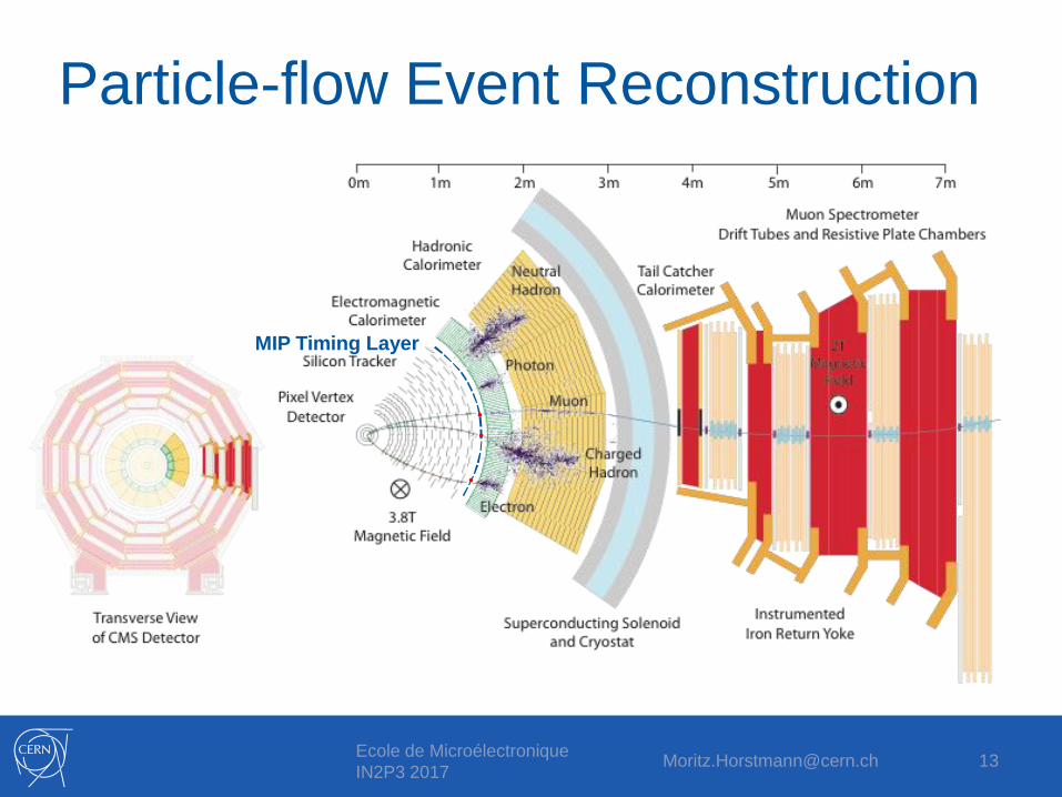
Time Measurements• Start – stop measurement
• Measurement of time interval between two local events:Start signal – Stop signal
• Used to measure relatively short time intervals with high precision
• For small systems (1 channel)
• Like a stop watch for a local event
• Time tagging• Measure time of occurrence of events in relation to a
given time referenceTime reference (Clock) Events to be measured (Hit)
• Used to measure relative occurrence of many events on many channels on a defined time scale
• Such a time scale will have limited range but can be circular (e.g. LHC machine orbit time)
• For large scale HEP systems
• Like a normal watch with a common 24h scale
17
Start
Stop
Time scale (clock)
Ch1
Ch2
ChN
Ecole de Microélectronique
IN2P3 [email protected]

Interface to front-end and time
walk compensation schemes• Basic discriminator
• Significant time walk (depending on signal slew rate)
• Double threshold• Interpolate to “0” volt amplitude
• Needs two discriminators and two TDC channels, Limited efficiency reported in practice.
• TDC plus pulse amplitude (peak or charge) measurement with ADC• ADC measurement expensive and
slow (may be needed anyway)
18
Time walk
Thr
Thr2
Thr1
Time walk
Thr
Amp1
Amp2
Ecole de Microélectronique
IN2P3 [email protected]

• Constant Fraction Discriminator: CFD• Compensate directly in discriminator
• Works very well for fixed pulse shape with varying amplitude.
• Needs delay: Made as distributed RC within ASIC (but also works as filter)
• If signal shape not constant, then?
• Leading edge + Time Over Threshold (poor mans ADC)• Minimal extra hardware
(also measure falling edge time)
• Has been seen to work quite well in several applications.
• If signal shape not constant then?
• TOT now very often seen in HEP for indirect amplitude measurement with moderate resolution
19
Original
Delayed
Fraction of
originalCrossing point
independent
of amplitude
Enable (thresholded)
Time walk
Thr
TOT
Thr
Ecole de Microélectronique
IN2P3 [email protected]

• Alternative: Very fast analog sampling• Pulse matching – highest possible
flexibility and performance
• High power – low channel density
• 64GHz 8b ADC’s now feasible, 2W• 100GbE optical
• Large amount of data to read out and process (unless done on chip).
• Multiple sampling capacitor array chips made in HEP community
• Sampling rate: 1 – 5Gs/s
• Analog bandwidth: Few hundred MHz -GHz
• Resolution: 8 – 12 bits
• Memory size
• Channel count
• Triggering - Buffering
• ADC
• Readout
20Ecole de Microélectronique
IN2P3 [email protected]

Time measurement• Coarse count: ~1ns
• Multi GHz counters can be made in modern ASIC’s.
• Gray code• Only one bit changing
• Dynamic range: Large
• 1st. Level fine interpolation: • Extract timing difference between signal and
reference (clock)• Dynamic range: 1 (2) clock cycle
• A: Use same interpolation reference as counter (Clock).
• B: Use Different “reference”
• Alignment between coarse and fine needs special care.
• Must be done with precision of full resolution
• If badly done then large error (coarse count) in small time window around coarse time change.
• Example: Use of two phase shifted binary counters and selecting one based on fine interpolation.
21
Counter
Register
Clock
Hit
N N+1 N+2 N+3 N+4 N+5
N N+1 N+2
0 – 1 clock
1 – 2 clocks
Clock
Cnt
Hit
Coarse
Fine
Fine
Start
Stop
N N+1
N N+1
Clock
Cnt1
Cnt2
Coarse counter
Ecole de Microélectronique
IN2P3 [email protected]

Time to amplitude• Time to Amplitude Conversion: TAC
• Classical type high resolution TDC implemented with discrete components
• Delicate analog design
• Requires ADC
• Slow conversion time –> dead time
• Not using same reference as coarse time
• Dual slope Wilkinson ADC/TDC• Time stretcher
• Measure stretched time with counter
• Slow: Analog de-randomizer
• Example: NA62 GTK in-pixel design
22
Start
Stop ADC
V
Start Stop
Start/stop
Stop/start
I
I/k
V
Start Stop
II/k
T= (1+k)(Stop- Start)
C
I
T*I\C
Ecole de Microélectronique
IN2P3 [email protected]

Delay line based• Basic principle
• Use “gate” (inverter) delays • Normally two inverters
• Gate delays have large process, voltage and temperature dependency
• Using inverting cell• Rise and fall time ( N and P transistors) does
not match well over process, voltage and temperature.
• Different tricks can be used to make inverting and non inverting buffer have “same” delay but remains problematic.
• Fully “digital”
• Capture:• Use hit as clock to capture state of delay chain
• Use delay signals to capture state of hit signal (high speed sampler)
• Delay Locked Loop• Control delay chain to cover exactly one
clock cycle.• Compensates for Process, Voltage and
Temperature effects (but not miss-match)
• Uses same timing reference as course count and self calibrates to this.
• Begin-end effects, Phase error, Jitter, Delay cell matching
• Such a delay locked loop is a very quite circuit as all transitions are perfectly distributed over clock period(not the case for the Hit signal)
• Half digital / half analog`
Register
Start
Stop
Register
Clock
Hit
PDCharge
pump
Start
23
Register
PDCharge
pump
Hit
Clock
Ecole de Microélectronique
IN2P3 [email protected] 23

Delay elements• Current starved inverters/buffers
• N-side, P-side, Both
• Only one of the two current starved
• Regulate delay chain power supply with local LDO• Careful interfacing to other circuits
• Differential delay cell• Consumes DC power -> More power
• Only needs one cell per delay (better resolution)
• (Less sensitive to power supply noise)
• (Generates less noise)
• Different types of loads can be used• Inductive peaking can gain ~20%
• ~25ps possible in 130nm, worst case
• Pseudo differential and many more
24
LDO
VDD
CP
In
Bias
Bias
In
Bias
24
Ecole de Microélectronique
IN2P3 [email protected]

Sub-gate delay. 2nd. interpolation
• Vernier principle• Difference in delays can be made
much smaller than delay in cell R=T2-T1
• Basic Vernier chain gets impractical long
• Performance gets mismatch dominated
• Delay difference can be implemented in many ways:
• Capacitance loading
• Transistor sizing
• Different current starving
• etc,.
• How to lock to reference ?• DLL’s locked to different references
• DLL’s with different number of delay cells locked to same reference.
25
T1
T2
Start
Stop
Ecole de Microélectronique
IN2P3 [email protected]

DLL arrays• An array of DLL’s can use
the Vernier principle• DLL’s auto lock to common
timing reference
• Example: Improve binning from 25ps to 6.25ps• 4 equal DLL’s driven by fifth
DLL with slightly larger delay• Potentially very mismatch
sensitive
• 1 DLL driving many small DLL’s
• Less mismatch sensitive(mismatch correction still advantageous)
• Non trivial layout to assure matching routing capacitances and R-C delays
26
Clock
PD
PD
PD
PD
PD
T1T2 = T1 + Δ
Resolution: T2 – T1 = Δ
PLL
1.25GHzDLL
Coarse counter
21 bit
25ps
DLL DLLDLL
2 x 21 bit
4 x 32 time taps
25ps + 6.26 ps
T1
T2=5/4T14
5
Ecole de Microélectronique
IN2P3 [email protected]

• Passive delays• In modern IC technologies wiring
delays already the dominating source of delays.
• No easy way to “lock” to global reference• Some kind of adjustment required
• R-C delay• The adjustment of any tap affects all the other taps
• Used in HPTDC. In practice a bit of a pain (but works)
• Transmission line• Short delays can be made with on-chip transmission lines
• Predefined and characterized transmission lines exists in may chip design kits.
• Lossy so signal shape changes down the line.
• Can be used on hit signals instead of on DLL signals• Flexibility on channel count versus resolution (used in HPTDC)
• This scheme can be used with many approaches
27
PLL
320MHz
160MHz
40MHz
Mux
DLL
Coarse counter
R
C R
C R
C R
C
Hit
Ch0
Ch1
Ch2
Ch3
Ecole de Microélectronique
IN2P3 [email protected]

Looped Vernier (beating oscillators)• Two delay chains/loops propagates
timing signals with slightly different delay.• Start – Stop type
• Start oscillators with start and stop signals• Latch loop1 count (start) when stop
occurs
• Latch loop2 count (stop) when edge in loop2 catches up with edge in loop1.
• Store in which Vernier cell the twoedges meet.
• Appears elegant but hard to implement:• Loop feedback time and re-coupling must
be “zero” delay• Circular layouts tried (but not so good for
matching)
• All this per channel
• No direct lock to a reference
• Long conversion time -> Dead-time
• Some errors accumulate during recirculation
28
T1
T2
Start
Stop
Cnt1
Cnt2
Ver
Start
Stop
Cnt1
Coarse
Cnt2
Fine time interpolation
expanded to be sum of
Cnt2 plus Vernier
Vernier point
where loop2
edge ”meets”
with Loop 1 edge
Ecole de Microélectronique
IN2P3 [email protected]

Analog interpolation between delay cells
• Resistive voltage division across neighbor delay cells.• Rise times in delay chain longer than
delay of cell.
• Purely resistive division “autoscales” with delay of delay cell
• Only carries current during transitions.
• Parasitic capacitance makes this resistive division a mixture of resistive division and R-C delays• Relatively low resistor values required
to prevent being R-C dominated.
• With equal resistances the bins are not evenly spaced -> re-optimize individual resistors
• Does not any more fully “autoscale” to delay of delay cell.
• Can be done on single ended and differential delay cells
29
R R R R R R R R
Delay cell
Ecole de Microélectronique
IN2P3 [email protected]

Time amplifier in “metastable window” of latch (with internal feedback).
• Any type of latch has a small time window where it enters a metastable region and it takes some time to resolve this
• A small change of timing on the input gives a “large” change of timing on the output: Time Amplifier
• For very high time resolution cases.• Only small window where time
amplification occurs
• Non linear, very sensitive to power supply, etc.
• Hard to use in practice
• For 3rd level interpolation
Plus other “exotic” schemes.
• (implementation nightmare)
30
0 1
10ps10ps
1ns
Ecole de Microélectronique
IN2P3 [email protected]

Ecole de Microélectronique
IN2P3 [email protected] 31
Wave Union TDC
● multiple measurements on single channel● need to sample the HIT (data driven structure)● often used in FPGAs to overcome large bin sizes

Central timing block• For multi channel TDC’s it is attractive to
have a central timing block used to drive array of individual channels• Minimal complexity per channel.
• Only one block to calibrate.
• Power consumed in timing block less critical (but timing distribution to channels gets significant)
• For very high resolution TDC’s this gets increasing difficult as required signal propagation delays larger than required resolution (mismatch!).
• Buffer delays large than resolution: miss-match sensitive
• For highly distributed TDC functions on large chips (e.g. pixel chips) it gets routing and power prohibitive even for low time resolution.• Alternative: Centralized DLL locked to reference
generates control voltage to distributed delay loops (miss-match !)
32
Centralized timing
block locked to
global reference
(e.g. DLL array)
RegisterCh0
RegisterCh1
RegisterChN
Reference
(Clock)
Ecole de Microélectronique
IN2P3 [email protected]

Time capture registers• The latches/registers used to capture the
timing event get critical in the ps range
• Fast capture/regeneration registers required• Timing signals have large rise/fall times
compared to required resolution.
• Small and well defined metastability window with good resolving capability.
• Single ended (e.g. classical master slave FF) or differential (sense amplifier for fast SRAM’s)
• Mismatch between registers• Assuming multiple registers must latch at same
instance
• Routing of hit signal to registers must be done with care
33Ecole de Microélectronique
IN2P3 [email protected]

Capture Scheme
SynchronousSample state of hit signal
Continuous data flow
Potentially no dead time
AsynchronousSample state of reference signal
Sample only when actual hit
occurs -> lower power
Ecole de Microélectronique
IN2P3 [email protected]

HPTDC• History
• Architecture initially developed at CERN for ATLAS MDT (design transferred to KEK)
• CMS Muon and ALICE TOF needed similar TDC with additional features / increased resolution
• Features• 32 channels(100ps binning),
8 channels (25ps binning)
• 40MHz time reference (LHC clock)
• Leading, trailing edge and TOT
• Triggered or non triggered
• Highly flexible data driven architecture with extensive data buffering and different readout interfaces
• Used in large number of applications:• More than 20 HEP applications: ALICE TOF, CMS muon,
STAR, BES, KABES, HADES, NICA, NA62, AMS, Belle, BES, , ,
• We still supply chips from current stock, running out
• Other research domains: Medical imaging,
• Commercial modules from 3 companies: CAEN, Cronologic, Bluesky
• ~50k chips produced
• 250nm technology (~10 years ago for LHC)• Development: ~5 man-years + 500kCHF.
• Can not be produced any more
• http://tdc.web.cern.ch/TDC/hptdc/docs/hptdc_manual_ver2.2.pdf
35
PLL
320MHz
160MHz
40MHz
Mux
DLL
Coarse counter
Hit register 0
Hit register 1
Hit register 2
Hit register 3
Hit
cont.
R-C
R-C
X 8
Channelarbitration
Encoding
Offset adjust
L1 buf fer 256
Reject counterTrigger matching
Match window
X 4
Bunch count
Event count
Trigger interface
Trigger FIFO
Trigger matching
control
16
Readout FIFO
Round Robin
JTAG:
Boundary scanProgrammingMonitoringStatusProduction test
Error monitoring:
Memories
State machines
Measurements
Programming
JTAG
Readout interface
Parallel Byte Serial
256
Clock
(40MHz)
Hit[31:0]
Trigger
Resets
JTAG
Token-in Token-outReadout
32 15 bit
INL RC mode
-5
-4
-3
-2
-1
0
1
2
3
4
5
1 101 201 301 401 501 601 701 801 901 1001
bin17ps RMS
Ecole de Microélectronique
IN2P3 [email protected]

Ecole de Microélectronique
IN2P3 [email protected] 37
Difficulties in ps range resolution
● In sub-ps resolutions device mismatches can become dominant-> careful simulation & dimensioning during design time-> can have major impact on design
● Power supply noise-> short delays, fast edges-> separate power domains-> substrate isolation-> clean PCB layout
● Distribution of signals get critical-> RC delay of wires-> balanced distribution of timing critical signals
● Process-Voltage-Temperature variations-> LSB auto calibration to compensate for slow VT variations-> global offset calibration still required
LSB/sqrt(12) ≠ rms
DNL, INL
Noise, Jitter
Offset shifts
single-shot precision

Ecole de Microélectronique
IN2P3 [email protected] 38
System Level
● Detector Noise● Analog Front End● Time Walk Correction● Time Reference Noise● TDC Noise● Inter-channel Crosstalk● PVT variation ...
Complete Measurement Chain

Ecole de Microélectronique
IN2P3 [email protected] 39
Delay Element
Fast = Short Propagation Delays = More robust design
● CMOS inverterdouble inverterpseudo differential
● Fully Differentialshort propagation delay w/ controlmore robust against power supply noise
(depends on design)cross-coupled load / low power
● Current starved / Voltage Controlledlarge propagation delay variationsslower cell due to controlNMOS / PMOS
For fine-time TDC designs:
● Critical building block - often longest delay path / used in many architectures
In
Bias
Bias
In
Bias

Ecole de Microélectronique
IN2P3 [email protected] 40
Time Capture Registers● Critical building block - makes timing decision
● Latchsimple / small areatiming information can be overwritten
● Fully Differential Flip-Flopstatic current consumptionfully differential inputno conversion if differential signaling
● Standard D Flip-Flophit independent readout outsingle-ended
Fine resolution = good matching / high powerOR
Fine resolution = FF calibration
For fine-time TDC designs:
sense-amplifier FF

Requirements
• achieve sub 10ps LSB sizes
➢ with RMS better than bin-size
• ~64 channels
• large dynamic range
➢ allow to use one common reference
• robust against power supply noise
• flexible in terms of power consumption / time
resolution
Ecole de Microélectronique
IN2P3 [email protected] 43

TDC Trends
44
New detectors and sensors require new TDC
integrationresolution
● 3ps binning (1-2ps RMS)● High integration● Flexible
Ecole de Microélectronique
IN2P3 [email protected]

Ecole de Microélectronique
IN2P3 [email protected] 45
picoTDC Architecture
© IEEE
• Central interpolator with
counter to extend dynamic
range
• Measurements are referenced
to common reference to allow
to synchronize multiple TDCs
• DLL for PVT auto calibration
and power consumption trade-
off
• Short propagation delays and
fast signal slopes of timing
critical signals to reduce jitter
• Calibration applied on two
groups of channels to reduce
circuit overhead and
calibration time
• Relatively constant power
consumption make it less
sensitive to change in hit rate

Low Jitter PLL• Clock multiplication from 40MHz to
2.56GHz for fine time counter and
time interpolator
• Low jitter critical
• Jitter filtering of 40MHz clock to the
extent possible
• 40MHz reference MUST be very clean
• LC based oscillator
• Design: Jeffrey Prinzie, KU Leuven
• Detailed layout and optimization
• Prototyped May 2015
• Measurements very promising
(350fs RMS jitter)
46Ecole de Microélectronique
IN2P3 2017
Phase Noise vs. Freq. Offset

Ecole de Microélectronique
IN2P3 [email protected] 47
Fine-Time Interpolator
● DLL to control LSB size-> 64 fast delay elements in first stage - 12 ps-> total delay of DLL 781 ps at 1.28 GHz
● Resistive Interpolation to achieve sub - gate delay resolutions-> LSB size of 2nd stage controlled by DLL
12 psdelays
3 psdelays
1.28 GHzN=64

Ecole de Microélectronique
IN2P3 [email protected] 48
Voltage Controlled Delay Cell
δ ∝𝐶𝑒𝑓𝑓 ⋅ 𝑉𝑂𝑠𝑐
𝐼𝐵𝑖𝑎𝑠
approximate propagation delay
● fully differential cell● voltage controlled● single ended output
post layout extracted simulation
12 ps < 16 ps < 23 ps

Operation Region (Post Layout)
• Running at all corners @12ps delay
Ecole de Microélectronique
IN2P3 2017

DLL• 64 taps, 12.2ps delay
• Self-Calibrating
• Jitter not as critical,
doesn’t pile up
Ecole de Microélectronique
IN2P3 201750
1 3 5 7 9 111315171921232527293133353739414345474951535557596163
-2E-12
-1E-12
000E+0
1E-12
2E-12
3E-12
4E-12
5E-12
Jitter (RMS) INL DNL

Resistive Interpolation and Drivers• Interpolation can be disabled for low resolution
mode
• Drivers: tapered buffers, each driving 32 capture FFs and 64 standard cell FFs
• Calibration separate for each half
Ecole de Microélectronique
IN2P3 [email protected]

Ecole de Microélectronique
IN2P3 [email protected] 52
Resistive Interpolation
● resistive voltage divider-> signal slopes bigger than delay
● RC delay (capacitive loading)- > use small resistances, small loads

Calibration
• 5 bit for each channel
• Up to +24ps with 750fs steps
Ecole de Microélectronique
IN2P3 [email protected] 53

Ecole de Microélectronique
IN2P3 [email protected] 55
Device Mismatch
● Calibration can correct for Fine-Time Interpolator and Distribution Buffer mismatch● Don't want to calibrate each single register
-> time capture registers require good matching
standard deviation of LSBacross all bins
1.2ps RMS
830fs RMS

Ecole de Microélectronique
IN2P3 [email protected] 56
Time Capture Register
1st Latch highly optimized for timing
σTDC = 0.8 ps RMS
no calibration in FF:
Trade off: power & resolution

Time Capture Flip Flops• Revisited design, timing vs. power very critical, 16k
capture Flip Flops running @1.28GHz
• Highly optimized M/S Flip Flop followed by standard cell Flip Flop for metastability resolution
• Monte Carlo simulations show a mismatch of 800fs RMS, noise influence of 240fs RMS
Ecole de Microélectronique
IN2P3 201757
D
CLK
Q D
CLK
QHit input
Clock
Phase
M/S-FF Std.C. FF
Out

Hit Decoding
• Decoding fully synchronous
• One pipeline register at each clock phase per channel
• 3 coarse or 4 fine pipeline stages
• In each stage signal phases move closer together
• Result in center of capture channel / phases
Ecole de Microélectronique
IN2P3 [email protected] 58

Full Timing Macro
Ecole de Microélectronique
IN2P3 201759
• 64 channels, DLL and resistive interpolator in the center
• Hit signal input on the left, output on the right

Post Layout Power Consumption
• DLL + resistive interpolation: 40mW
• Time distribution + calibration: 260mW
• Capture registers: 250mW
• Decoding: 50mW
➢ Total @ 3ps bins: 600mW
➢ Total @ 12ps bins: 200mW
Ecole de Microélectronique
IN2P3 [email protected]

Hit Receivers • Differential receivers optimized for ultra-low jitter, low power
• Full Range (common mode 0V .. VDD=1.2V), somewhat LVDS-compatible
• Highest speed @~800mV common mode
• Optimized for 200mv Peak-Peak amplitude
• Design: Bram Faes, KU Leuven
• Prototyped & tested
Ecole de Microélectronique
IN2P3 [email protected]

Sources of Measurement Deviation• Bin size 3ps -> 880fs RMS
• PLL: 350fs RMS phase Jitter
• DLL&Drivers : 400fs RMS phase Jitter, INL/DNL can be calibrated down to ~400fs
• Capture FFs: 800fs mismatch (DNL)
• Hit receivers: <1ps jitter
➢ ~1.75ps RMS total deviation
• External sources: input clock jitter, signal pre-processing
Ecole de Microélectronique
IN2P3 [email protected]

Full picoTDC Architecture
63
64 channels, 3ps or 12ps time binning, 200us dynamic range
Ecole de Microélectronique
IN2P3 [email protected]

TDC Logic
• Synthesized logic from SystemVerilog RTL
• Based on data driven architecture from HPTDC
• Simplifications with individual buffers per channel
• Clocking: 320 MHz
• Trigger matching based on time measurements
• Extensive verification environment
• New interfaces defined and implemented
• Control/monitoring, Trigger, Readout
64Ecole de Microélectronique
IN2P3 [email protected]

Logic Features
• Untriggered or triggered with configurable latency and length, overlap possible
• Naturally overflowing counter used for calculating trigger matches, TOT etc.
• Counter with arbitrary overflow and reset for machine cycle, can be inserted in event header when triggered or in measurements when untriggered
• Combination of TOT+untriggered+arbitrarycounter overflow should preferably be removed, adds a lot of logic overhead
Ecole de Microélectronique
IN2P3 [email protected]

Interfaces• Power: 1.2v, ~1.0W (64ch, 3ps),
~0.5W (64ch, 12ps)~0.3W (32ch, 12ps)
• Hits: Differential (LVDS “compatible”)
• Time reference: 40MHz differential• Low jitter reference critical for high time resolution
• Trigger/Event-Rst/BX-Rst/reset: Sync Yes/No • Option: encoded protocol?
• Control/monitoring: I2C at CMOS 1.2V-levels• Option: GBT E-link?
• Readout: 4 readout ports of 1-8 differential signals• Common mode 0.6V, programmable current 1-4mA
• Compatible with LpGBT and FPGAs
• Packaging: ~340 FPBGA
66Ecole de Microélectronique
IN2P3 [email protected]

Constraints on Input Signals
• Max. one edge per 1.28GHz-Cycle (~0.8ns)
• Internal glitch filter• Filter time can be programmed to enforce the 0.8ns
or more for filtering e.g. oscillations
• Small derandomizer (4 hits) for each channel running @1.28GHz
• Sustainable rate to channel buffer 320MHz, trigger matching running @320MHz for each channel separate
➢ No bottlenecks until readout buffers
• Trigger in each 40MHz-Cycle possible
Ecole de Microélectronique
IN2P3 [email protected]

Readout• 1 or 4 readout ports
• 4 ports: High rate applications (e.g. non triggered)16 TDC channels per port
• 1 port: Low-medium rate64 channels (or 32 channels in 32 channel mode)Round robin with channel group separators, max. consecutive hits per group can be configured
• Readout data: 32bit words• Headers, trailers, TDC data, status, etc.
• Readout ports interface• Byte wise:
• 40, 80, 160, 320 MHz
• Option: Sync signal to mark first byte of word
• Serial:• 8B/10B encoding
• Low speed: 40, 80, 160, 320 Mbits/s
• High speed: 1.28 Gbits/s
• TDC readout bandwidth: • Max:
320MHZ x 8 x 4 = 10Gbits/s ( ~4Mhits/s per channel without triggering)1.28Gbits/s x 4 = 5Gbits/s
• Min: 1 x 40Mbits/s= 40Mbits/s
68Ecole de Microélectronique
IN2P3 [email protected]

Absolute TDC data
Ecole de Microélectronique
IN2P3 201770
Full TDC data, DEFAULT FORMAT
Relative to Trigger

Leading + TOT
Ecole de Microélectronique
IN2P3 201771
• Packet Type: 1bit
• Channel ID: 4 bits, for single port readout +2 bit group separator
• Leading: 16/19 bits• Large dynamic range
• 16bit 3ps resolution: 200ns
• 19bit 3ps resolution: 1600ns
• Programmable part of full 25bits leading TDC
• (Relative to trigger to be useable)
• TOT (Relative to leading): 11/8 bits• Short dynamic range:
• 8bit 3ps resolution: 780ps
• 11bit 3ps resolution: 6.1ns
• Programmable part of full 25bits TOT difference• TOT assumed to be used for offline time-walk correction of leading.
• Alternative: Readout of Individual Leading and Trailing edges with full range/resolution• 2x readout bandwidth

Verification Environment
Ecole de Microélectronique
IN2P3 201773
• Verification in SystemVerilog
• Use cases can be defined and automatically tested, visualization of
buffer occupancy, lost hits etc.
Verification Features
• Environment supports and verifies all TDC
features
• Triggered / untriggered
• Rising / rising&falling / TOT
• Different counter and reset settings
• Extensive test cases
• High / low / burst hit rate
• High / low trigger rate, overlapping triggers
• Specific use cases can be defined, verified
Ecole de Microélectronique
IN2P3 [email protected]


Backup

[email protected] Delay-Locked Loops 77
Outline - Delay-Locked Loops
• DLL overview
• Building blocks:
– VCDL
– PD
– LF
• DLL analysis:
– Linear
– Nonlinear
• Lock acquisition
• Charge sharing

[email protected] Delay-Locked Loops 78
Why Delay-Locked Loops?
Ext. CLK Clockpad
DLL
clock route
QOutput
pad
Int. CLK
IC
External clock
Internal clock
Output data
Phase aligned
Output data registers delay
Clock skew control
The DLL automatically nulls theskew between these two points
Clock buffers andinterconnectsintroduce delay
DLL delay + Clock buffers + Clock route delay = Clock period
Phases 0 and 2p are
indistinguishable
Dt ≠ T

[email protected] Delay-Locked Loops 79
DLL Block Diagram
Delay-Locked Loop functional blocks
• Voltage Controlled Delay Line (VCDL):
– Takes the reference clock as an input
and delays it by some amount D.
– The delay D is function of a control
voltage D(Vcontrol).
– Sometimes the control quantity can be
a current. In this case we have a
Current Controlled Delay Line (CCDL)
– We will assume that the higher the
voltage (or the current) the shorter will
be the propagation delay through the
delay line.
• Phase Detector (PD):
– Compares the phase of the signal at the input and output of the VCDL.
– Depending on the type, produces an error signal that:
• It is proportional to the phase difference between the input and output phases;
• It just gives an indication on the sign of the phase error (bang-bang detector).
• Loop filter (LF):
– Eliminates the high frequency components of the error signal:
– It can be implemented as:
• An RC low-pass filter
• An active low pass filter
• A charge-pump and a capacitor
1st order
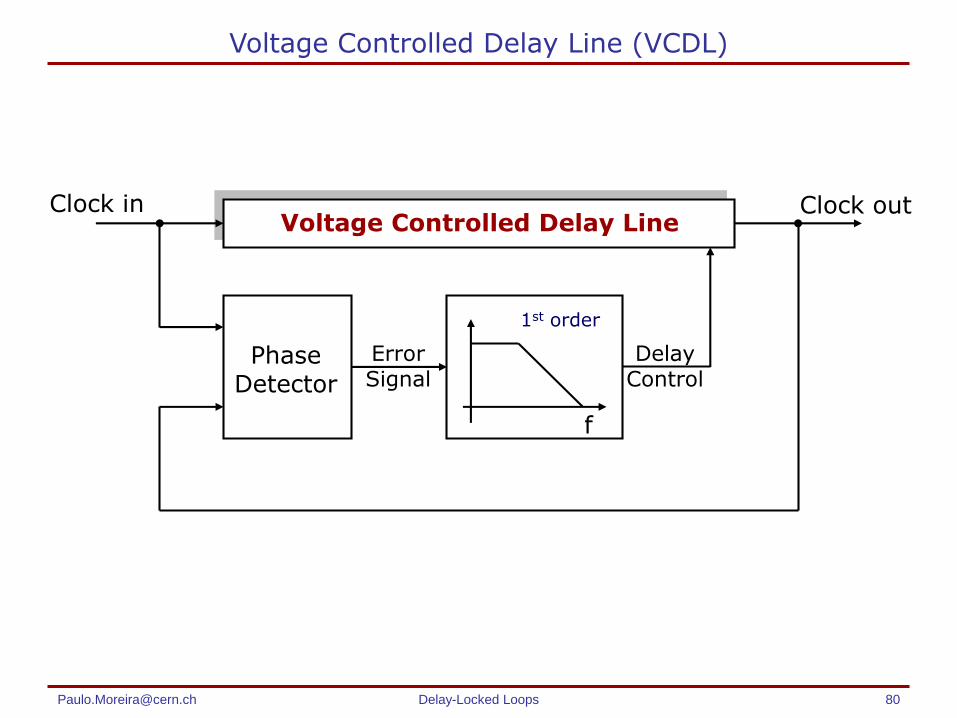
[email protected] Delay-Locked Loops 80
Voltage Controlled Delay Line (VCDL)
Voltage Controlled Delay Line
PhaseDetector
f
1st order
ErrorSignal
DelayControl
Clock in Clock out

[email protected] Delay-Locked Loops 81
Intrinsic Delay in CMOS Circuits
VIN
0
Vdd
t
VOUT
0
Vdd
t
50% leveldelay
CVIN
VGS
I (VGS-VT)2
Ideal MOS
Assuming VT ≈ 0
W
L
VC
CV
I
Ct
ddox
dd
Dm2
Time it takes to discharge
C from Vdd to Vdd/2

[email protected] Delay-Locked Loops 82
CMOS Inverter
• Common-source configuration:
– NMOS can only discharge (pull-down);
– PMOS can only charge (pull-up);
– Both P and N transistors are thus
needed.
• CMOS inverter:
– No static power consumption.
• Mobility electrons > mobility holes:
– PMOS transistors are weaker than
NMOS.
– To compensate:
Wp/Wn = mn/mp ≈ 3/1 (for Ln = Lp,
typically minimum length in digital
circuits).
• What’s the best way to control the
inverter delay:
– Vdd?
– CL?
– None of the two!
in
out
Vdd
CL
in out
[email protected] Delay-Locked Loops 83
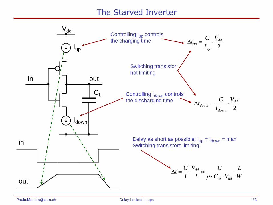
The Starved Inverter
Vdd
in
out
CL
in out
Iup
Idown
2
dd
up
up
V
I
Ct D
2
dd
down
down
V
I
Ct D
W
L
VC
CV
I
Ct
ddox
dd
Dm2
Controlling Iup controls
the charging time
Controlling Idown controls
the discharging time
Switching transistor
not limiting
Delay as short as possible: Iup = Idown = max
Switching transistors limiting.

[email protected] Delay-Locked Loops 84
Biasing the Starved Inverter
Vdd
CL
in out
Vcontrol
Ibias = Iup/N
Iup
Idown
1:N

[email protected] Delay-Locked Loops 85
Making Sure it Will Work
• Can we run the starved inverter
infinitely slow?.
• No, must have:
Vdd
CL
in out
Vcontrol
Iup
Imin1
0
1
0
input
output
Pulse wide enough
Pulse appears delayed at the output
Pulse too shortinput
outputFiltered out by the
starved inverter
)widthpulsemin(fallrise tt
Imin prevents trise and tfall
from becoming too long

[email protected] Delay-Locked Loops 86
In a real implementationthese nodes introducepoles in the VCDL transferfunction. Care must betaken so they are at highfrequencies not to disturbthe DLL dynamic behavior.
Voltage Controlled Delay Line
Vdd
in out
Vcontrol
Iup
Imin
td = f(Vcontrol) = Kvcdl × Vcontrol(linear approximation valid around the working point)

[email protected] Delay-Locked Loops 87
Differential Delay Cell
Advantages:
• ‘Insensitive’ to common-mode;
• Signal and the Inverted signal
available.
• Constant power consumption: low
switching noise
Vdd
in+
Vcontrol
Iup
Imin
in-
out- out+
1 1 1
1 2
Disadvantages:
• Consumes static power;
• Half of the tail current used to
charge/discharge the load;
• Differential to single ended converter
required to interface with CMOS logic

[email protected] Delay-Locked Loops 88
The Phase Detector (PD)
Voltage Controlled Delay Line
PhaseDetector
f
1st order
ErrorSignal
DelayControl
Clock in Clock out

[email protected] Delay-Locked Loops 89
The DFF Phase Detector
• Sign information only:
– No phase error magnitude information;
– It distinguishes early or late only;
– It is called a bang-bang phase detector.
• Loop operation:
– When in lock the phase change occurs
virtually every clock cycle and the
average phase error becomes zero.
• Its advantages are:
– simplicity of operation;
– Operation possible at the maximum FF
operation frequency;
– Minimum pulse width 1/f;
– The phase range spans from –p to +p.
– Insensitive to duty-cycle distortion in
the CK input (however: duty-cycle
distortion on the D input creates
asymmetry in the transfer function)
input
output
error
Output lags the input
input
output
error
Output leads the input
D QVCDL input signal
VCDL output signal
error
p-p
vdd
0

[email protected] Delay-Locked Loops 90
DFF PD Implementation
• Carefully design one.
• To avoid phase errors and
Metastability:
– Internal nodes same fanout;
– Gates the same driving
capability;
– Every two gates in the same
latch same fan-in;
– The latch SR1 is critical
should reach its final state as
fast as possible;
– Decision in a fraction of the
reference clock period
Otherwise increased jitter.
• Layout is critical for operation:
– Device matching;
– Large area devices;
– Layout as symmetrical as
possible;
– Keeping the wire loading
identical on corresponding
nodes.
D
Dummy
gate
Dummy
gate
SR1
SR2
SR3

[email protected] Delay-Locked Loops 91
The Loop Filter (LF)
Voltage Controlled Delay Line
PhaseDetector
f
1st order
ErrorSignal
DelayControl
Clock in Clock out

[email protected] Delay-Locked Loops 92
Capacitor: A Current Integrator
• Consider what happens when a current
is fed to a capacitor:
• The voltage across the capacitor (V) is
simply the time integral of the current
(I) being fed to the capacitor:
• We can thus easily integrate the phase
error if we feed to a capacitor a
current that is proportional to the
phase error ‘measured’ by the phase
detector:
0
0
1VdttI
CtV
t
V
I
tt
err dttIC
dtt00
1
)()( ttI err

[email protected] Delay-Locked Loops 93
Active Loop-filter: Charge-Pump + Capacitor
0
0
))(()()( VdttsignC
ItVtV
t
err
cp
capcontrol
D QVCDL
in
VCDLout
late
early
Icp
Icp
Vcap
Vcontrol
Vcontrol
error
Late = lag sign(err) = 1Early = lead sign(err) = -1

[email protected] Delay-Locked Loops 94
Charge-Pump for Bang-Bang Detector
• M1: current sink,
M2: current source;
• M3 and M4: switches:
– Alternatively closed and opened:
– Current always flows into or out of the
filter capacitor (never directly between
Vdd and ground);
• Reference leads:
– M4 closed, M3 opened
– Control voltage increases.
• VCO leads:
– M3 closed, M4 opened
– Control voltage decreases
• Keep sink and source currents well
matched:
– minimize static (average) phase error;
• Charge sharing effects need be
controlled (discussed later).
Vdd
C
Icp
M2
M3
M4
M1
error Vcontrol

[email protected] Delay-Locked Loops 95
The Delay-Locked Loop
Voltage Controlled Delay Line
PhaseDetector
f
1st order
ErrorSignal
DelayControl
Clock in Clock out

[email protected] Delay-Locked Loops 96
Bang - Bang Operation Overview
Q
Q
DLate
Early
in out
Vcontrol
in
out
Early Late Late Late Early Late

[email protected] Delay-Locked Loops 97
Bang-Bang Operation Tradeoffs
Tracking jitter:
• The loop tracking behavior introduces
jitter:
– In lock output phase constantly
oscillates back and forward around the
phase of the reference signal:
– It is a result of no phase error
magnitude information.
• Possible to reduce the loop tracking
jitter to insignificant levels;
• Other jitter sources:
– Thermal and shot noise;
– Substrate noise;
– Power supply noise.
Tradeoffs:
• Optimization for low-jitter:
– Increase the loop-capacitor C;
– Decrease: Icp and Kvcdl.
• Optimization for fast-lock:
– Decrease the loop-capacitor C;
– Increase: Icp and Kvcdl.
• Optimization for low-jitter and fast-
lock:
– It is possible to optimize for both:
– Use a large Icp during lock-acquisition;
– Use a small Icp after locking.
• Optimization against substrate and
power supply noise:
– Same as for fast-lock;

[email protected] Delay-Locked Loops 98
DLL: linear analysis
• Loop filter:
– Charge-pump + capacitor.
• Phase detector:
– Considered Linear signal
proportional to the phase error.
• Phase detector output:
– Pulse of duration proportional to the
phase error (e.g. DT(high)-DT(low) in an
XOR phase detector).
PD dt
VCDL
• Continuous time approximation:
– Valid for bandwidths a decade or more
below the operating frequency.
(Keep in mind that DLLs are in fact non-
linear devices.)
• A single pole is present in the loop
filter:
– The DLL is a 1st order network.
• Combination charge-pump and loop-
capacitor:
– Acts as a perfect integrator;
– Modeled as an integrator.

[email protected] Delay-Locked Loops 99
DLL Modeling
Choice of variables:
• DLL response formulated in terms:
– Input delay;
– Output delay;
• Output delay:
– The VCDL delay: DO(t) or DO(s)
• Input delay:
– The delay to which the phase detector
compares the output delay: DI(t) or
DI(s)
• Note that DI(t):
– It is phase detector dependent;
– It s frequency dependent;
VCDL
)()( sVKsD contvcdlO
)(sVcont
PD)(sDO T
sDsD
T
t OI )()( -
D
Phase detector outputis active during this fractionof the reference period
dtCs
I
T
t cp
DcontV
T
tD

[email protected] Delay-Locked Loops 100
DLL Transfer Function
PDs
1
DO(s)
n
I
O
ssD
sDsH
1
1
)(
)()(
CT
KI vcdlcp
n
vcdl
cpOIO K
Cs
I
T
sDsDsD
-
)()()(
Phase error
Charge pumpDuty-cycle
Control voltage
VCDL propagation delay
• The closed loop transfer
function is 1st order
• It is characterized by the
natural frequency n

[email protected] Delay-Locked Loops 101
The DLL is a 1st Order System
• Designing a DLL it is equivalent to
choose its natural frequency n:
– Choose Icp and C.
– Kvcdl ‘fixed’ by the VCDL design
and technology parameters (some
degree of control but not much).
– T is fixed by the operation
frequency/frequencies.
– Since the system is 1st order it is
inherently stable:
• Make sure the higher order,
unwanted but unavoidable, poles
are at least 10 times higher that n.
• The closed-loop behavior is similar to
that of a 1st order low-pass RC filter:
– Settling to 2% t ≈ 4t
– Settling to 0.1% t ≈ 7t
• Fast settling requires large n:
– Trades off against low tracking jitter.
– n might start approaching the higher
order poles.
CT
KI vcdlcp
n
t
Dfinal
nt
1
t
final
t
D
dt
tDd
0
)(n naturally ‘tracks’
the reference frequency.

[email protected] Delay-Locked Loops 102
DLL Design
• The parameters:
– Icp
– C
– Kvcdl
are technology, temperature and
supply voltage dependent
• n would track the operation
frequency (i.e. proportional to 1/T) if
the other parameters were ‘absolutely’
constant:
– Self-biasing techniques can make n
track the operation frequency over
several decades: see Maneatis 1996
• Example:
– F = 100 MHz
T = 10 ns
– Icp = 1 mA
– C = 100 pF
– Kvcdl = 2 ns/V
This leads to:
– n = 2 krad/s
– t = 0.5 ms
Notice that:
• The DLL bandwidth is many orders of
magnitude lower than the operation
frequency.
• When locked to a low jitter clock signal
this PLL will display low tracking jitter.
• A VCDL, when subjected to substrate
or power supply noise, will generate
jitter. Under such circumstances, a DLL
with such a low bandwidth will be
ineffective tracking the input phase
and thus suppressing its own jitter.
CT
KI vcdlcp
n

[email protected] Delay-Locked Loops 103
Bang-Bang DLL Nonlinear Analysis
➢ When a DLL uses a DFF as the phase
detector, the continuous time
approximation can not be used.
➢ Simple expressions can be found for:
– The response to a period step;
– The tracking jitter.
Phase step:
The new period is 2/3×Ti < Tf < 2×Ti:
– DLL will regain lock to the new phase;
– The VCDL delay will ramp to the new
value.
• The new period is outside the above
bounds:
– The Phase-Detector will give the wrong
phase information and the DLL will lose
phase lock.
C
IK
td
VdK
dt
tDd cp
vcdlcontrol
vcdl )(
The DLL will try to catch the new periodat a rate given by:
Units: [rad/s] or [s/s]
Example:Using the previous example the tracking slope is: 20 ns/ms
Reference
VCDLTinitial
Tfinal
t
Period

[email protected] Delay-Locked Loops 104
Frequency Step f2 > f1
in VCDL out
Q
Q
DLate
Early
C.P.
The DLL is locked to thereference signal (period T1)
Immediately after the frequencystep (period T2 < T1) the VCDLdelay is too big and the PD willactivate the late signal until thede VCDL propagation delaybecomes equal to T2
VCDLpropagationdelay
VCDLinputperiod
T1
in
out
in
out
T2 < T1 Phase is detectedlate, the VCDLdelay is goingto be decreased.

[email protected] Delay-Locked Loops 105
Frequency Step f1 > f2
in VCDL out
Q
Q
DLate
Early
C.P.
The DLL is locked to thereference signal (period T1)
Immediately after the frequencystep (period T1 < T2) the VCDLdelay is too short and the PD willactivate the early signal until thede VCDL propagation delaybecomes equal to T2
VCDLpropagationdelay
VCDLinputperiod
T1
in
out
in
out
T2 > T1
Phase is detected early, the VCDLdelay is going to be increased.

[email protected] Delay-Locked Loops 106
Frequency Step: Limit Values
If T2 < 2/3 T1 the phase detectorwill activate the early output insteadof the late. The delay will increaseinstead of decreasing.
If T2 > 2 T1 the phase detectorwill activate the late output insteadof the early. The delay willdecrease instead of increasing.
T1
T2
in
out
in
out
T1
T2
in
out
in
out

[email protected] Delay-Locked Loops 107
Bang-Bang Tracking Jitter
• Ideally every clock cycle the phase-
detector should alternate between an
early and a late decision.
• In practice, due to charge-pump
unbalance or jitter, it is very likely that
the PD decision will be frequently
maintained during two consecutive
clock cycles to either side.
• The minimum P-P tracking jitter is
thus given by:
Jitter:
• Uncertainty on the position of the falling and rising edges.
• Seen in a scope as ‘thick’ traces on the rising and falling
positions.
T
in
out Jitter
TC
IKT
dt
tDd cp
vcdl 4)(
4
TC
IV
cp
cont D 4
early
late
contVD
Example:Using the tracking slope from the previous example:
Jpp = 4 × (20 ns/ms) × (10 ns)Jpp = 0.8 ps
The tracking jitter can be thus made to be very small. The jitter is likely to be dominated by thermal, supply and substrate noise.

[email protected] Delay-Locked Loops 108
DLL Lock Acquisition
Typical Bang-Bang DLL startup procedure:
1. Set the VCDL to its minimum value
(maximum control voltage)
2. Force the VCDL delay to increase until
the phase detector gives a consistent
early indication (e.g. 32 consecutive
early detections)
3. Once the PD consistently indicates
early, pass the control of the loop to
the phase detector which will finally
take the DLL to lock.
in
out
1st phaseVCDL set to itsminimum delay
Here the PD wrongly indicates late
in
out
2nd phase
Here, due to jitter, the PD sometimes givesthe correct and sometimes the wrong indication
in
out
3rd phase
The PD is now in a ‘safe’ zone, it correctly andconsistently indicates early.

[email protected] Delay-Locked Loops 109
Charge Sharing
• Charge-pumps perform almost like ideal integrators however charge sharing might
degrade their performance.
Vdd
C
Icp
M2
M3
M4
M1
late Vcontrol
This node charges to Vdd when M4 is open
This node discharges to gnd when M3 is open
Cd2
Cd1
cont
d
dcont V
CC
CV
-D
1
1
)(2
2contdd
d
dcont VV
CC
CV -
D
When M4 closes Vcontrol jumps of:
When M3 closes Vcontrol jumps of:
Notice that:• The voltage jump is proportional to thecontrol voltage itself;• ≈ proportional to Cd1 and Cd2;• ≈ inverse proportional to C;(usually C>> Cd1 or Cd2):
Example:If C = 100 pF, Cd1 = 10 fF and Vcontrol = 1V:
DVcontrol = -100 mV
Compare with: Icp×T/C = 100 mV

[email protected] Delay-Locked Loops 110
Charge Sharing Control
• Charge sharing is eliminated.
• Clock feed-through is present
through Cgd of M5 and M6.
However the voltage swing at
the gate of these transistors is
relatively small
Vdd
C
lateVcontrol
Icp
Icp
M1
M2
M3
M4
M5
M6
Voltage on this node never dropsmuch below Vth. So turn-on isrelatively fast.
Voltage on this node never risesmuch above Vdd-Vth. So turn-onis relatively fast.
RC time constant

[email protected] Delay-Locked Loops 111
Delay chain feed through
Vdd
in out
Vcontro
l
Iup
Imin
Parasitic Cdg introduces
ripple on the control lines.
In lock the raising
and falling edges
effects cancel each
other.
To maintain
symmetry,
buffer the dummy
cell control lines.

Ecole de Microélectronique
IN2P3 [email protected] 115
Code Density Test
● Before Global Calibration
● Uniformly distributed events across clock cycle- asynchronous clock domains
● Number of collected hits => bin size
T
average LSB = 5ps
σLSB = 2.1 ps

Ecole de Microélectronique
IN2P3 [email protected] 116
Interpolator Linearity
● After Global Calibration LSB = 5ps
σLSB = 1.3 ps
no missing codes
Integral- Non-LinearityDifferential-Non-Linearity
σLSB = 2.1 ps
before calibration:
after calibration:

Ecole de Microélectronique
IN2P3 [email protected] 117
DNLafter global calibration
DNL = ± 0.9 LSB
RMS < 0.28 LSB (1.4 ps-rms)
© IEEE
no missing codes

Ecole de Microélectronique
IN2P3 [email protected] 118
INLafter global calibration
expected rms resolution w/ custom FF:including quantization noise, INL & DNL
INL = ± 1.3 LSB
RMS = < 0.43 LSB (2.2 ps-rms)
2.3 ps-rms < σqDNL/wINL < 2.9 ps-rms
ideal 5 ps LSB TDC: 1.44 ps-rms
© IEEE
(could correct for INL offline)

TWEPP 2013 L. Perktold / J. Christiansen 119
Reconstructed Transfer Functionafter global calibration
has been applied
DNL
INL
channel 5

Ecole de Microélectronique
IN2P3 [email protected] 120
Standard Cell FF - Weak MatchingIntegral- Non-LinearityDifferential-Non-Linearity
DNL = +2 LSB / -1 LSB
RMS = < 0.69 LSB (3.45 ps-rms)
INL = ±2.5 LSB
RMS = < 0.87 LSB (4.35 ps-rms)
expected time resolution: < 5.9 ps-rms (w/ standard cell FF)

Ecole de Microélectronique
IN2P3 [email protected] 121
Double Shot Measurement Principle● Uniformly distributed events across 1 clock cycle
- asynchronous clock domains
● Send same hit to two distinct channels
● Delay fixed by wire length differences
● Jitter contribution of hit not canceled out
Sigma
Single Shot Resolution in ps
Sigma*5ps/sqrt(2)
bin difference

Ecole de Microélectronique
IN2P3 [email protected] 122
Measured Single Shot Precision● Three measurement series
- both hits arriving within one reference clock cycle- second hit arrives one clock cycle later - second hit arrives multiple clock cycles later (~5ns)
● limited by non-linearities of TDC-> very silent setup-> robust architecture
σTDC < 2.44 ps-rms
bin difference

Ecole de Microélectronique
IN2P3 [email protected] 123
Inter Channel Crosstalk● sweep hit B over hit A
● monitor change in delay of hit A
Pattern Generator artifactssmaller ± 1 LSB

Ecole de Microélectronique
IN2P3 [email protected] 124
PVT variations
-0.2 ps / mV
0.4 ps / deg
● constant delay path changes with VT
● different characteristic for different i/o


![The Story of Picosecond Ultrasonicsperso.univ-lemans.fr/~pruello/Picosecond ultrasonics from lab to... · The Story of Picosecond Ultrasonics 1 Christopher Morath, ... [ps] 0.00 0.05](https://img.pdfslide.us/doc/110x75/5a8820a97f8b9aa5408e58d4/the-story-of-picosecond-pruellopicosecond-ultrasonics-from-lab-tothe-story-of.jpg)