Embed Size (px)
Citation preview

2010 Microchip Technology Inc. DS51911A
PIC24FJ256DA210Development Board
User’s Guide

Note the following details of the code protection feature on Microchip devices:
• Microchip products meet the specification contained in their particular Microchip Data Sheet.
• Microchip believes that its family of products is one of the most secure families of its kind on the market today, when used in the intended manner and under normal conditions.
• There are dishonest and possibly illegal methods used to breach the code protection feature. All of these methods, to our knowledge, require using the Microchip products in a manner outside the operating specifications contained in Microchip’s Data Sheets. Most likely, the person doing so is engaged in theft of intellectual property.
• Microchip is willing to work with the customer who is concerned about the integrity of their code.
• Neither Microchip nor any other semiconductor manufacturer can guarantee the security of their code. Code protection does not mean that we are guaranteeing the product as “unbreakable.”
Code protection is constantly evolving. We at Microchip are committed to continuously improving the code protection features of ourproducts. Attempts to break Microchip’s code protection feature may be a violation of the Digital Millennium Copyright Act. If such actsallow unauthorized access to your software or other copyrighted work, you may have a right to sue for relief under that Act.
Information contained in this publication regarding deviceapplications and the like is provided only for your convenienceand may be superseded by updates. It is your responsibility toensure that your application meets with your specifications.MICROCHIP MAKES NO REPRESENTATIONS ORWARRANTIES OF ANY KIND WHETHER EXPRESS ORIMPLIED, WRITTEN OR ORAL, STATUTORY OROTHERWISE, RELATED TO THE INFORMATION,INCLUDING BUT NOT LIMITED TO ITS CONDITION,QUALITY, PERFORMANCE, MERCHANTABILITY ORFITNESS FOR PURPOSE. Microchip disclaims all liabilityarising from this information and its use. Use of Microchipdevices in life support and/or safety applications is entirely atthe buyer’s risk, and the buyer agrees to defend, indemnify andhold harmless Microchip from any and all damages, claims,suits, or expenses resulting from such use. No licenses areconveyed, implicitly or otherwise, under any Microchipintellectual property rights.
DS51911A-page 2
Trademarks
The Microchip name and logo, the Microchip logo, dsPIC, KEELOQ, KEELOQ logo, MPLAB, PIC, PICmicro, PICSTART, PIC32 logo, rfPIC and UNI/O are registered trademarks of Microchip Technology Incorporated in the U.S.A. and other countries.
FilterLab, Hampshire, HI-TECH C, Linear Active Thermistor, MXDEV, MXLAB, SEEVAL and The Embedded Control Solutions Company are registered trademarks of Microchip Technology Incorporated in the U.S.A.
Analog-for-the-Digital Age, Application Maestro, CodeGuard, dsPICDEM, dsPICDEM.net, dsPICworks, dsSPEAK, ECAN, ECONOMONITOR, FanSense, HI-TIDE, In-Circuit Serial Programming, ICSP, Mindi, MiWi, MPASM, MPLAB Certified logo, MPLIB, MPLINK, mTouch, Octopus, Omniscient Code Generation, PICC, PICC-18, PICDEM, PICDEM.net, PICkit, PICtail, REAL ICE, rfLAB, Select Mode, Total Endurance, TSHARC, UniWinDriver, WiperLock and ZENA are trademarks of Microchip Technology Incorporated in the U.S.A. and other countries.
SQTP is a service mark of Microchip Technology Incorporated in the U.S.A.
All other trademarks mentioned herein are property of their respective companies.
© 2010, Microchip Technology Incorporated, Printed in the U.S.A., All Rights Reserved.
Printed on recycled paper.
ISBN: 978-1-60932-286-1
2010 Microchip Technology Inc.
Microchip received ISO/TS-16949:2002 certification for its worldwide headquarters, design and wafer fabrication facilities in Chandler and Tempe, Arizona; Gresham, Oregon and design centers in California and India. The Company’s quality system processes and procedures are for its PIC® MCUs and dsPIC® DSCs, KEELOQ® code hopping devices, Serial EEPROMs, microperipherals, nonvolatile memory and analog products. In addition, Microchip’s quality system for the design and manufacture of development systems is ISO 9001:2000 certified.

PIC24FJ256DA210DEVELOPMENT BOARD
USER’S GUIDE
Table of Contents
Preface ........................................................................................................................... 5
Chapter 1. Introducing the Development Board1.1 Introduction ................................................................................................... 111.2 Development Board Features ...................................................................... 111.3 Power Requirements .................................................................................... 131.4 Companion Display Boards .......................................................................... 141.5 Typical Development Board Configurations ................................................. 151.6 Development Board Demonstration Programs ............................................. 151.7 Additional Software for Application Development ....................................... 16
Chapter 2. The Demonstration Application2.1 Introduction ................................................................................................... 172.2 About the Application ................................................................................... 17
Chapter 3. Programming and Debugging the Board3.1 Introduction ................................................................................................... 193.2 Tutorial overview .......................................................................................... 193.3 Loading the Project ...................................................................................... 203.4 Building the Code ......................................................................................... 223.5 Programming the PIC24FJ256DA210 .......................................................... 233.6 Running the Code ........................................................................................ 263.7 Debugging the Code .................................................................................... 27
Chapter 4. Development Board Hardware4.1 Introduction ................................................................................................... 314.2 Functional Overview ..................................................................................... 314.3 General Hardware Features ......................................................................... 324.4 Setup and Configuration ............................................................................... 34
Appendix A. Development Board SchematicsA.1 Introduction .................................................................................................. 49A.2 Hardware Features ...................................................................................... 49A.3 Development Board Schematics .................................................................. 51
Appendix B. Modifications for PICtail Plus Daughter BoardsB.1 Introduction .................................................................................................. 59B.2 Overview of the PICtail Plus Interface ......................................................... 59B.3 Modifications for Specific Daughter Boards ................................................. 62
Index ............................................................................................................................. 63
Worldwide Sales and Service .................................................................................... 64
2010 Microchip Technology Inc. DS51911A-page 3

PIC24FJ256DA210 Development Board User’s Guide
NOTES:
DS51911A-page 4 2010 Microchip Technology Inc.

PIC24FJ256DA210DEVELOPMENT BOARD
USER’S GUIDE
Preface
INTRODUCTION
This chapter contains general information that will be useful to know before using the PIC24FJ256DA210 Development Board. Items discussed in this chapter include:
• Document Layout• Conventions Used in this Guide• Recommended Reading• The Microchip Web Site• Training and Seminars• Development Systems Customer Change Notification Service• Customer Support• Document Revision History
DOCUMENT LAYOUT
This document describes how to use the PIC24FJ256DA210 Development Board as a development tool to emulate and debug firmware on a target board. The manual layout is as follows:
• Chapter 1. Introducing the Development Board provides a brief overview of the PIC24FJ256DA210 Development Board, its features and its uses.
• Chapter 2. The Demonstration Application provides a brief overview of the interactive, touch-screen-based demo that ships with the development board.
• Chapter 3. Programming and Debugging the Board provides instructions for using MBLAB® IDE to create a project and program the development board.
• Chapter 4. Development Board Hardware provides a detailed description of the development board’s features and instructions on their configuration.
• Appendix A. Development Board Schematics provides the schematics and other technical details.
• Appendix B. Modifications for PICtail Plus Daughter Boards provides specific directions for adapting the development board to interface with daughter boards.
NOTICE TO CUSTOMERS
All documentation becomes dated, and this manual is no exception. Microchip tools and documentation are constantly evolving to meet customer needs, so some actual dialogs and/or tool descriptions may differ from those in this document. Please refer to our web site (www.microchip.com) to obtain the latest documentation available.
Documents are identified with a “DS” number. This number is located on the bottom of each page, in front of the page number. The numbering convention for the DS number is “DSXXXXXA”, where “XXXXX” is the document number and “A” is the revision level of the document.
For the most up-to-date information on development tools, see the MPLAB® IDE on-line help. Select the Help menu, and then Topics to open a list of available on-line help files.
2010 Microchip Technology Inc. DS51911A-page 5

PIC24FJ256DA210 Development Board User’s Guide
CONVENTIONS USED IN THIS GUIDE
This manual uses the following documentation conventions:
DOCUMENTATION CONVENTIONS
Description Represents Examples
Arial font:
Italic characters Referenced books MPLAB® IDE User’s Guide
Emphasized text ...is the only compiler...
Initial caps A window the Output window
A dialog the Settings dialog
A menu selection select Enable Programmer
Quotes A field name in a window or dialog
“Save project before build”
Underlined, italic text with right angle bracket
A menu path File>Save
Bold characters A dialog button Click OK
A tab Click the Power tab
Text in angle brackets < > A key on the keyboard Press <Enter>, <F1>
Courier New font:
Plain Courier New Sample source code #define START
Filenames autoexec.bat
File paths c:\mcc18\h
Keywords _asm, _endasm, static
Command-line options -Opa+, -Opa-
Bit values 0, 1
Constants 0xFF, ‘A’
Italic Courier New A variable argument file.o, where file can be any valid filename
Square brackets [ ] Optional arguments mcc18 [options] file [options]
Curly brackets and pipe character: { | }
Choice of mutually exclusive arguments; an OR selection
errorlevel {0|1}
Ellipses... Replaces repeated text var_name [, var_name...]
Represents code supplied by user
void main (void){ ...}
DS51911A-page 6 2010 Microchip Technology Inc.

Preface
RECOMMENDED READING
This user's guide describes how to use PIC24FJ256DA210 Development Board. Other useful documents are listed below. The following Microchip documents are available and recommended as supplemental reference resources.
PIC24FJ256DA210 Data Sheet (DS39969)
Consult this document for detailed information on the PIC24FJ256DA210 microcon-troller with integrated graphics controller. Reference information found in this data sheet includes:
• Device memory map• Device pinout and packaging details• Device electrical specifications• List of peripherals included on the device
PIC24F Family Reference Manual
This reference manual explains the operation of the PIC24F microcontroller family architecture and peripheral modules. The specifics of each device family are discussed in the individual family’s device data sheet. This useful manual is online located in the Technical Documentation section of the Microchip web site. Refer to these for detailed information on PIC24F device operation.
MPLAB® ASM30, MPLAB® LINK30 and Utilities User’s Guide (DS51317)
This document helps you use Microchip’s language tools for PIC24F devices based on GNU technology. The language tools discussed are the MPLAB ASM30 Assembler, MPLAB LINK30 Linker, MPLAB LIB30 Archiver/Librarian and other 16-bit device utili-ties.
MPLAB® C30 C Compiler User’s Guide (DS51284)
This document helps you use Microchip’s MPLAB C30 C compiler to develop your application. MPLAB C30 is a GNU-based language tool, based on source code from the Free Software Foundation (FSF). For more information about FSF, see www.fsf.org.
MPLAB® IDE User’s Guide (DS51519)
This document describes how to use the MPLAB Integrated Development Environment (IDE), as well as the MPLAB IDE Project Manager, MPLAB IDE Editor and MPLAB SIM Simulator. Use these development tools to help you develop and debug application code.
MPLAB® IDE Simulator, Editor User’s Guide (DS51025)
Consult this document for more information pertaining to the installation and implemen-tation of the MPLAB IDE software.
Graphics Solutions and Capacitive mTouch™ Sensing Documentation
The Microchip web site provides a wealth of information for developing microcon-troller-based solutions using graphics and touch sensing. Application notes and soft-ware libraries are available to help design and implement applications. Refer to www.microchip.com/graphics and www.microchip.com/mtouch for more information.
2010 Microchip Technology Inc. DS51911A-page 7

PIC24FJ256DA210 Development Board User’s Guide
THE MICROCHIP WEB SITE
Microchip provides online support via our web site at www.microchip.com. This web site is used as a means to make files and information easily available to customers. Accessible by using your favorite Internet browser, the web site contains the following information:
• Product Support – Data sheets and errata, application notes and sample programs, design resources, user’s guides and hardware support documents, latest software releases and archived software
• General Technical Support – Frequently Asked Questions (FAQs), technical support requests, online discussion groups, Microchip consultant program member listing
• Application and Market Support – Specific information on Microchip’s latest solutions for targeted vertical markets and hardware solutions, including ready-to-use application libraries to support the latest hardware
• Business of Microchip – Product selector and ordering guides, latest Microchip press releases, listing of seminars and events, listings of Microchip sales offices, distributors and factory representatives
TRAINING AND SEMINARS
Microchip offers classes and training in Regional Training Centers (RTCs) conveniently located worldwide. The RTCs offer a variety of highly-targeted design topics that can help in creating new applications, adding functionality to existing applications, or taking full advantage of new and unfamiliar device peripherals on PIC devices and dsPIC® DSCs. These classes can help in keeping current in the competitive and always chang-ing world of embedded design, and stay ahead of industry trends and design tech-niques. Visit the RTC web site at www.microchip.com/rtc site for details on offered classes.
In addition, Microchip also offers various a wide-ranging line of online webinars that are available at all times. For those users who may not have the ability to attend a class in person, or the time to wait for a class to be offered, these provide a convenient alter-native that is available on your schedule. For more information, visit the web sites www.microchip.com/webinars.
DS51911A-page 8 2010 Microchip Technology Inc.

Preface
DEVELOPMENT SYSTEMS CUSTOMER CHANGE NOTIFICATION SERVICE
Microchip’s customer notification service helps keep customers current on Microchip products. Subscribers will receive e-mail notification whenever there are changes, updates, revisions or errata related to a specified product family or development tool of interest.
To register, access the Microchip web site at www.microchip.com, click on Customer Change Notification and follow the registration instructions.
The Development Systems product group categories are:
• Compilers – The latest information on Microchip C compilers and other language tools. These include the MPLAB C18 and MPLAB C30 C compilers; MPASM™ and MPLAB ASM30 assemblers; MPLINK™ and MPLAB LINK30 object linkers; and MPLIB™ and MPLAB LIB30 object librarians.
• Emulators – The latest information on Microchip in-circuit emulators, such as the MPLAB ICE 4000.
• In-Circuit Debuggers – The latest information on the Microchip in-circuit debuggers, MPLAB ICD 3 and MPLAB REAL ICE.
• MPLAB® IDE – The latest information on Microchip MPLAB IDE, the Windows® Integrated Development Environment for development systems tools. This list is focused on the MPLAB IDE, MPLAB SIM simulator, MPLAB IDE Project Manager and general editing and debugging features.
• Programmers – The latest information on Microchip programmers. These include the MPLAB PM3 and PRO MATE II device programmers and the PICSTART® Plus, PICkit™ 3, MPLAB ICD 3 and MPLAB REAL ICE™ development programmers.
CUSTOMER SUPPORT
Users of Microchip products can receive assistance through several channels:
• Distributor or Representative• Local Sales Office• Field Application Engineer (FAE)• Technical Support
Customers should contact their distributor, representative or field application engineer (FAE) for support. Local sales offices are also available to help customers. A listing of sales offices and locations is included in the back of this document.
Technical support is available through the web site at: http://support.microchip.com
DOCUMENT REVISION HISTORY
Revision A (June 2010)
• Initial Release of this Document.
2010 Microchip Technology Inc. DS51911A-page 9

PIC24FJ256DA210 Development Board User’s Guide
NOTES:
DS51911A-page 10 2010 Microchip Technology Inc.

PIC24FJ256DA210DEVELOPMENT BOARD
USER’S GUIDE
Chapter 1. Introducing the Development Board
1.1 INTRODUCTION
The PIC24FJ256DA210 Development Board is an efficient, low-cost development plat-form to evaluate the features and performance of Microchip’s PIC24FJ256DA210 microcontroller. The 16-bit microcontroller integrates a high-performance graphics con-troller, CTMU and USB OTG modules essential for integrated human interface applica-tions. Supporting this is a range of user-defined interfaces, USB options and memory expansions for the maximum flexibility in developing graphics-capable solutions. A range of Microchip development tools and software environments, along with a range of application libraries, simplifies the process of software development.
Topics discussed in this chapter include:
• Development Board Features
• Power Requirements
• Companion Display Panels
• Typical Development Board Configurations
• Development Board Demonstration Programs
• Additional Software for Application Development
1.2 DEVELOPMENT BOARD FEATURES
The PIC24FJ256DA210 Development Board, shown in Figure 1-1, incorporates a range of features to enhance its usefulness as a platform for developing graphics applications. Key features are identified in Figure 1-2.
FIGURE 1-1: PIC24FJ256DA210 DEVELOPMENT BOARD
2010 Microchip Technology Inc. DS51911A-page 11

PIC24FJ256DA210 Development Board User’s Guide
FIGURE 1-2: PIC24FJ256DA210 DEVELOPMENT BOARD LAYOUT
1. PIC24FJ256DA210 Microcontroller (U2)
2. Potentiometer for analog input (R3)
3. Prototyping area
4. Three red user-defined LEDs, multiplexed with (8) and (9) (D1, D2 and D3)
5. Red user-defined LED on PMA17 address line (D4)
6. MCLR Reset Button (S4)
7. Microchip Display Connector V1 (J3)
8. Capacitive touch pads
9. Push button switches (S1, S2 and S3)
10. On-board 512 Kbyte SRAM (U6)
11. On-board 512 Kbyte Flash Memory (U5)
12. On-board 16 Mbit (2 Mbyte) SPI Flash Memory (U4)
13. PICtail™ Plus 120-pin expansion connector (J8)
14. On board 5V and 3.3V regulators for external 9V input (Q1 and Q2), and green LED power indicator (D6)
15. USB device mode interface (J2)
16. USB Host mode interface (J4)
17. USB On-The-Go mode interface (J7)
18. RS-232 (DB-9F) serial port and associated hardware (P1)
19. RJ-11 ICD programming/debugging connector (J10)
20. PICkit™ ICSP™ programming/debugging connector (J9)
21. 32.72 kHz secondary oscillator circuit (Y2 and U1)
22. 8 MHz crystal for primary microcontroller clock (Y1)
M
1
12
2 3 4 5
6
7
9 810111314
15
16
17
18
19
20 21 22
DS51911A-page 12 2010 Microchip Technology Inc.

Introducing the Development Board
1.2.1 PIC24FJ256DA210 Microcontroller
At the heart of the PIC24FJ256DA210 Development Board is the PIC24FJ256DA210 microcontroller. This microcontroller comes with a 16-bit core along with integrated graphics controller, as well as a wide range of peripherals.
The graphics controller is capable of running TFT, MSTN and CSTN display panels with resolution of up to QVGA (320x240) or WQVGA (480x272) at color depths of 16 bits per pixel (bpp), and VGA (640x480) running at 8 bpp. QVGA resolution can be run with the microcontroller’s internal 96 Kbyte of RAM at 8 bpp. Refer to the “PIC24FJ256DA210 Family Data Sheet” (DS39969) for details.
1.2.2 Graphics Interface
The development board uses Microchip’s standardized 64-pin edge connector to interface with compatible display boards. Both TFT and STN display boards can be accommodated, as well as many forms of resistive touch screen interfaces. Please refer to Section 4.4.4 “Graphics Port” for more details.
1.2.3 USB Options
As part of its standard peripheral set, the PIC24FJ256DA210 microcontroller supports full-speed USB operations with an on-chip controller and bus transceiver. In addition to Device mode operations, the USB controller supports Host and On-The-Go (dual-role) modes. The appropriate separate receptacles are provided for the required cable for each mode. Note, however, that only one of the USB modes can be active at any time.
1.2.4 Peripheral Options
Beyond the graphics and USB interfaces, the development board is equipped with an extensive set of additional features for hardware application development. User-defined push button switches, CTMU-based touch sensors, LEDs, serial commu-nications, and several varieties of external memory are provided to give the developer a full range of hardware options. Please refer to Chapter 4. “Development Board Hardware” for a complete discussion.
1.2.5 PICtail Plus Connector
The PICtail Plus connector makes it possible to connect to a range of PICtail Plus Daughter Boards, thus adding new functionality to an application under development. The connector can be configured for different signal routings to accommodate different daughter boards. Please refer to Section 4.4.6 “PICtail™ Plus Card Modular Expan-sion Connector” for more information.
1.3 POWER REQUIREMENTS
The PIC24FJ256DA210 Development Board can be powered from an external power supply, or by applying power directly to test points on the board itself. For simplicity, an unregulated 9V power supply is recommended (such as Microchip part number AC162039).
Care must be observed when connecting customized displays. The on-board regula-tors can supply up to 800 mA current combined. A separate external power supply may be needed for bigger displays. Please refer the chosen display panel power requirements for details.
2010 Microchip Technology Inc. DS51911A-page 13

PIC24FJ256DA210 Development Board User’s Guide
1.4 COMPANION DISPLAY BOARDS
The PIC24FJ256DA210 Development Board is compatible with all of the graphic dis-play panels shown in Figure 1-3. The demo code that is pre-programmed onto the development board is designed to work with the Graphics Display Truly 3.2” 240x320 Board. The Graphics Display Prototype Board (AC164139) can be used to connect a different display panel.
The development board has been designed to be compatible with any future Microchip display panel products. Compatible display panels will have a 64-pin edge connector that matches the RGB Display Connector (V1). The most current list of display panels is available at the Microchip web site.
FIGURE 1-3: MICROCHIP GRAPHIC DISPLAY BOARDS
Graphics Display Truly 3.2” 240x320 Board (AC164127-4)
Graphics Display Powertip 4.3” 480x272 Board (AC164127-6)
Graphics Display Prototype Board (AC164139)
DS51911A-page 14 2010 Microchip Technology Inc.

Introducing the Development Board
1.5 TYPICAL DEVELOPMENT BOARD CONFIGURATIONS
The typical connections to use the development board as shipped from the factory are shown in Figure 1-4. To run the pre-programmed demo application:
1. Connect the Truly 3.2” Display Board display into Display Connector V1 (depend-ing on the development board kit ordered, this may or may not be included with the development board)
2. Plug a 9V power supply into J1
To program the board for application development, use one of the two programming ports provided:
• J10, a 6-wire RJ-11 jack (for use with MPLAB ICD 3 and MPLAB REAL ICE programmers)
• J9, a 6-pin riser (for use with the PICkit 3 programmer)
See Section 4.3.5 “Programming and Debugging Interface” for additional details on the programming ports.
FIGURE 1-4: TYPICAL BOARD CONFIGURATION
1.6 DEVELOPMENT BOARD DEMONSTRATION PROGRAMS
The development board is pre-programmed with a demo application designed for the Truly 3.2” Display Board. The application automatically runs when power is applied to the board, and shows various Microchip Application Libraries integrated into a single application. The demo is described in more detail in Chapter 2. “The Demonstration Application”.
The application can be reconfigured to run on other display panels. To do this, the board must be reprogrammed with the proper HEX file. For directions on reprogram-ming the development board, see Section Chapter 3. “Programming and Debug-ging the Board”.
Additional demonstration programs are provided with the Microchip Graphics Library, discussed in the following section. Refer to the Graphics Library Help file for details on how to download and run the additional demo applications.
9V Power Supply (AC162039)
MPLAB® ICD3 Programmer/Debuggeror MPLAB REAL ICE™ In-Circuit Emulator
PICkit™ 3 Programmer
PIC24FJ256DA210 Development Board Truly 3.2” Display(AC164127-4)
OR
2010 Microchip Technology Inc. DS51911A-page 15

PIC24FJ256DA210 Development Board User’s Guide
1.7 ADDITIONAL SOFTWARE FOR APPLICATION DEVELOPMENT
The demo application that ships with the PIC24FJ256DA210 Development Board only demonstrates part of the microcontroller’s capabilities. To take full advantage of the microcontroller and the development platform, download and install these software tools from the Microchip web site (if you don’t already have them):
• A Microchip development environment, such as the latest version of MPLAB IDE
• A C compiler for PIC24 microcontrollers, such as the MPLAB C30 compiler
• One or more of the specialized Microchip Application Libraries
1.7.1 The Microchip Application Libraries
Microchip Application Libraries (MALs) provide developers the ability to quickly develop applications for their products. MALs contain different libraries and stacks supporting connectivity, communication interfacing and user interfaces.
For example, using the Microchip Graphics Library provides ready-made library objects and drivers. Adding connectivity to applications is simplified with the MCHPFSUSB Library (full-speed USB) and/or the Microchip TCP/IP Stack. All of these stacks and libraries also come with their own demo software and examples, aiding users on how to integrate these software components into their applications.
Some of the available Application Libraries that will be useful in developing applications for the development board include:
• Microchip Graphics Library
• MCHPFSUSB Library
• mTouch™ Capacitive Library
• Microchip Memory Disk Drive (MDD) File System Interface Library
• Microchip TCP/IP Stack (with the addition of optional hardware)
Refer to the individual application library web page and documentation for details.
DS51911A-page 16 2010 Microchip Technology Inc.
PIC24FJ256DA210DEVELOPMENT BOARD
USER’S GUIDE
Chapter 2. The Demonstration Application
2.1 INTRODUCTION
This chapter provides a brief overview of the pre-programmed graphics demonstration application that is provided with the PIC24FJ256DA210 Development Board.
2.2 ABOUT THE APPLICATION
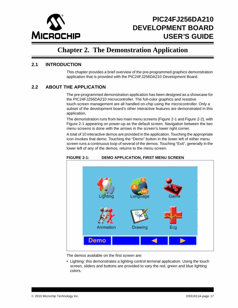
The pre-programmed demonstration application has been designed as a showcase for the PIC24FJ256DA210 microcontroller. The full-color graphics and resistive touch-screen management are all handled on-chip using the microcontroller. Only a subset of the development board’s other interactive features are demonstrated in this application.
The demonstration runs from two main menu screens (Figure 2-1 and Figure 2-2), with Figure 2-1 appearing on power-up as the default screen. Navigation between the two menu screens is done with the arrows in the screen’s lower right corner.
A total of 10 interactive demos are provided in the application. Touching the appropriate icon invokes that demo. Touching the “Demo” button in the lower left of either menu screen runs a continuous loop of several of the demos. Touching “Exit”, generally in the lower left of any of the demos, returns to the menu screen.
FIGURE 2-1: DEMO APPLICATION, FIRST MENU SCREEN
The demos available on the first screen are:
• Lighting: this demonstrates a lighting control terminal application. Using the touch screen, sliders and buttons are provided to vary the red, green and blue lighting colors.
2010 Microchip Technology Inc. DS51911A-page 17

PIC24FJ256DA210 Development Board User’s Guide
• Language: this shows how multiple languages can be integrated into one applica-tion. Text examples in Roman, Cyrillic, simplified Chinese, Japanese and Korean alphabets are shown.
• Game: this is a simple, interactive adaptation of a “snake” video game. Its operation is self-explanatory.
• Animation: this shows animation of stored graphics, along with image scaling and interactivity.
• Drawing: this demo implements free-hand drawing with a selectable color palette using the touch screen.
• ECG: this simulates an electrocardiogram display, demonstrating how analog data can be used to produce a graphic output. The “Ext” option switches between the fixed ECG display and a graphing display based on the potentiometer’s position.
FIGURE 2-2: DEMO APPLICATION, SECOND MENU SCREEN
The demos available from the second screen are:
• Clock: this is a simple numeric date and time display, based on the microcontroller’s RTCC.
• Graph Demo: this demo uses the Chart widget from the Microchip Graphics Library to generate a wide range of bar and pie charts based on a fixed set of data.
• External Flash: this demo shows images or pictures stored in the on-board Flash memory.
• Thumb Drive: this uses the USB Host interface to read a thumb drive connected to J4 and scan it for graphics files (JPEG or BMP formats only). The application then produces a directory of graphics images, and displays the corresponding file when selected.
2.2.1 Other Considerations
The demonstration application described here is the most current version as of the date of original publication of the user’s guide. Microchip Technology reserves the right to update this application and its appearance in future releases of the development board kit.
DS51911A-page 18 2010 Microchip Technology Inc.
PIC24FJ256DA210DEVELOPMENT BOARD
USER’S GUIDE
Chapter 3. Programming and Debugging the Board
3.1 INTRODUCTION
The PIC24FJ256DA210 Development Board may be used with MPLAB IDE, the free integrated development environment available on Microchip’s website. MPLAB IDE with Microchip’s compatible programming/debugging hardware allows the develop-ment board to be programmed and/or debugged.
For more information on how to use the MPLAB IDE, please refer to the following documentation:
• MPLAB IDE User’s Guide (DS51519)
• MPLAB IDE Quick Start Guide (DS51281)
• MPLAB IDE Online Help
This chapter includes the following:
• Tutorial Overview
• Loading the Project
• Building the Code
• Programming the PIC24FJ256DA210
• Running the Code
• Debugging the Code
3.2 TUTORIAL OVERVIEW
Creating projects with the Microchip Graphics Library requires that a number of files be included in the project. It is much more efficient to start a new project based on an exist-ing demo application release with the Microchip Graphics Library. The tutorial in this chapter uses that route to guide development of new applications. All demo applications are written in C for MPLAB C30.
The Demonstration Applications are provided with the Microchip Applications Library downloadable from http://www.microchip.com/mal. When installed in a specified path (for example,C:\Microchip Solutions\), the help file Graphics Library Help.chm is located in the path C:\Microchip Solutions\Micro-chip\Help\Graphics Library Help.chm. The help file contains the Graphics Library release notes and description of the API. It also contains useful information on the demo applications that can run on the development board.
Note: This tutorial was developed using MPLAB IDE v8.40 and MPLAB C30 Compiler v3.30 as the software tools, and the Microchip Graphics Applica-tions Library v2.10. Before proceeding, verify that you have at least these revision levels.
2010 Microchip Technology Inc. DS51911A-page 19

PIC24FJ256DA210 Development Board User’s Guide
Upon completing this tutorial, you should be able to:
• Load an existing project in MPLAB IDE
• Assemble and link the loaded project
• Debug the loaded project
• Program the PIC24FJ256DA210 with MPLAB REAL ICE in-circuit emulator or MPLAB ICD 3.
3.3 LOADING THE PROJECT
After installing the Microchip Graphics Library and the Demo Applications that are released with the library, load one of the demo applications to MPLAB IDE:
1. Launch MPLAB IDE.
2. Close any workspace that might be open (File > Close Workspace).
3. From the Project menu, select Open.
4. Browse through the directories to get to one of the several demo applications. The factory pre-programmed application is located in the path: C:\Microchip Solutions\Graphics MultiApp Demo\GMAP USB Demo PIC24.mcp. Click Open.
FIGURE 3-1: LOADING THE PROJECT
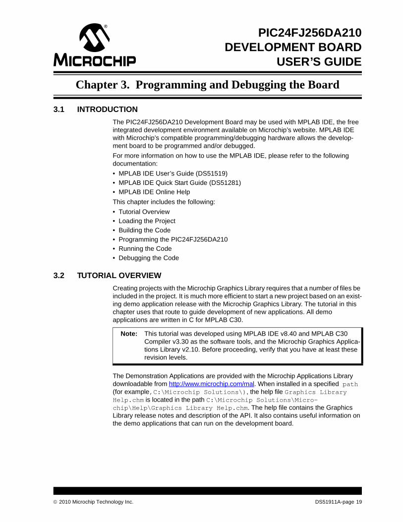
5. From the Configure menu, choose Select Device.
6. From the Device drop down list, select “PIC24FJ256DA210” (Figure 3-2). Click OK to select the device. The loaded project will be set to use MPLAB C30 compiler.
DS51911A-page 20 2010 Microchip Technology Inc.
Programming and Debugging the Board
FIGURE 3-2: SET DEVICE
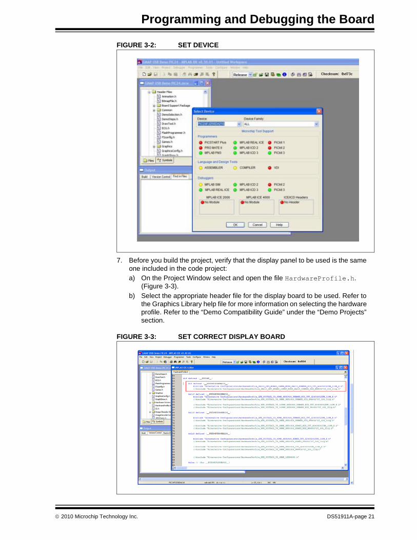
7. Before you build the project, verify that the display panel to be used is the same one included in the code project:
a) On the Project Window select and open the file HardwareProfile.h. (Figure 3-3).
b) Select the appropriate header file for the display board to be used. Refer to the Graphics Library help file for more information on selecting the hardware profile. Refer to the “Demo Compatibility Guide” under the “Demo Projects” section.
FIGURE 3-3: SET CORRECT DISPLAY BOARD
2010 Microchip Technology Inc. DS51911A-page 21

PIC24FJ256DA210 Development Board User’s Guide
3.4 BUILDING THE CODE
For the loaded project, building the code consists of compiling the source files to create an object file, GMAP USB Demo PIC24.o, then linking the object file to create the out-put files GMAP USB Demo PIC24.hex and GMAP USB Demo PIC24.cof. The HEX file contains the data necessary to program the device, and the .cof file contains additional information that lets you debug the code at the source code level.
3.4.1 Verifying the Compiler Path
Before building the project, check that the path of the MPLAB C30 compiler is set to the correct path. The path must be consistent with the location of the compiler when you installed it.
1. At the Project menu, click on Select Language Tool Suite… . This opens the Select Language Toolsuite dialog (Figure 3-4).
2. Verify that the C30 Toolsuite is selected in the Active Toolsuite list. In the Toolsuite Contents list, select each item, then verify the path for that item in the Location box. If necessary, modify the path by clicking on Browse, then browsing to and selecting the correct location in the dialog that follows.
3. After verifying and/or modifying the paths, click OK to exit.
FIGURE 3-4: SELECT LANGUAGE TOOLSUITE
3.4.2 Building the Project
Before building the project, set the build for a release version. From the menu bar of the main MPLAB IDE window, select Project > Build Configuration, then select Release.
To build the project in the main MPLAB IDE window, select Project > Make. The Build Output window appears (Figure 3-5).
Observe the progress of the build. When the “BUILD SUCCEEDED” message displays, you are ready to program the device.
DS51911A-page 22 2010 Microchip Technology Inc.

Programming and Debugging the Board
FIGURE 3-5: BUILD OUTPUT
3.5 PROGRAMMING THE PIC24FJ256DA210
Programming the PIC24FJ256DA210 is possible through any one of the following development hardware:
• MPLAB REAL ICE in-circuit emulator
• MPLAB ICD 2 or MPLAB ICD 3
• PICkit 3
• The MPLAB PM3 Universal Device Programmer
For this example, MPLAB REAL ICE in-circuit emulator is assumed to be used.
3.5.1 Set Up the Device Configuration
The device configuration for the PIC24F devices can be set by two methods:
• Using configuration macros in the source code
• Using the Configuration Bits window in MPLAB IDE
To display the Configuration Bits window, select Configure > Configuration Bits from the menu bar (Figure 3-6).
All demos that come with the Microchip Application Libraries include the configuration macros in the code. It is recommended to use these configuration settings in the code. To do this:
1. Open the Configuration Bits window.
2. Select the check box Configuration Bits set in code, located at the top of the window, to enable the use of the configuration in code.
For building applications that do not include configuration macros, it is possible to set the device configuration by using the Configuration Bits window. To do this:
1. Open the Configuration Bits window.
2. Set the Configuration bits by clicking on each line item and selecting an option from the drop-down menu that appears. The Configuration bits for the PIC24F device on the PIC24FJ256DA210 Development Board should be set as shown in Figure 3-6.
2010 Microchip Technology Inc. DS51911A-page 23

PIC24FJ256DA210 Development Board User’s Guide
FIGURE 3-6: PIC24FJ256DA210 DEVELOPMENT BOARD CONFIGURATION BITS
3.5.2 Connect and Enable MPLAB REAL ICE In-Circuit Emulator
1. Connect the MPLAB REAL ICE in-circuit emulator module to the PC with the USB cable.
2. Connect the MPLAB REAL ICE in-circuit emulator to the PIC24FJ256DA210 Development Board with the short RJ-11 cable.
3. Apply power to the development board.
4. From the Debugger menu, choose Select Tool > REAL ICE to set MPLAB REAL ICE in-circuit emulator as the debug tool in MPLAB IDE.
Once selected, MPLAB IDE will connect to the MPLAB REAL ICE in-circuit emulator and report that it has detected the module (Figure 3-7). Then it connects to the MPLAB REAL ICE in-circuit emulator verifying the firmware loaded on the module is appropri-ate for the selected device (PIC24FJ256DA210). If not, it will load the necessary firm-ware. Once the firmware is verified to be correct it connects to the development board and determines if the target device (i.e., the PIC24FJ256DA210) is present or not.
Note: Do not use the Configuration Bits window to set device configuration if con-figuration macros are already used in the source code. To do this, check the “Configuration Bits set in code” checkbox at the top of the Configuration bits window. Refer to the “MPLAB IDE Simulator, Editor User’s Guide” (DS51025) for additional information.
Note: Upon first connection to the PIC24FJ256DA210 Development Board, MPLAB IDE may need to download new firmware. Allow it to do so. If any errors are shown, double click the error message to get more information.
DS51911A-page 24 2010 Microchip Technology Inc.

Programming and Debugging the Board
FIGURE 3-7: ENABLING MPLAB® REAL ICE™ IN-CIRCUIT EMULATOR
3.5.3 Program the Device
From the Debugger menu, select Program to program the part. The Output window (Figure 3-8) displays the program steps as they occur.
Observe the results of the programming. When the “Programming/Verify complete” message appears, the device is programmed and ready to run.
FIGURE 3-8: PROGRAMMING THE DEVICE
2010 Microchip Technology Inc. DS51911A-page 25

PIC24FJ256DA210 Development Board User’s Guide
3.6 RUNNING THE CODE
The example application can either execute in real time (Run) or steps (Step Into, Step Over, and Animate.) Real-time execution occurs when you select Run in MPLAB IDE. Once the device code is halted, either by Halt or a breakpoint, you can step. The toolbar buttons (Figure 3-9) can be used for quick access to commonly used debug operations:
• Run
• Halt
• Animate
• Step Into
• Step Over
• Step Out
• Reset
FIGURE 3-9: DEBUGGING MENU OPTIONS
To see how these options function, do the following:
• Select Debugger > Reset > Processor Reset or click the Reset button to reset the program.
• Select Debugger > Run, or click the Run button. Observe how the application operates.
• Select Debugger > Halt, or click the Halt button to stop the program execution. A green solid arrow will mark the line of code in the File window where the program halted.
• Select Debugger > Step Into, or click the Step Into button, to step the program execution once. The green solid arrow will move down one line of code in the File window. Click the button several times to step through some code.
• Select Debugger > Reset > Processor Reset. Click the Reset button to reset the program again. The arrow will disappear, meaning the device is reset.
DS51911A-page 26 2010 Microchip Technology Inc.
Programming and Debugging the Board
3.7 DEBUGGING THE CODE
Assuming that you have modified the code to implement your own application on the PIC24FJ256DA210, it is possible that it will not work after your first build and needs to be debugged. MPLAB IDE provides an editor and several debug features, such as breakpoints and Watch windows, to aid in application code debugging.
This section includes:
• Editing Application Code
• Using Breakpoints and Mouseovers
• Using Watch Windows
3.7.1 Editing Application Code
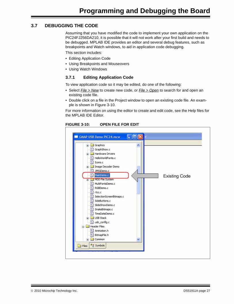
To view application code so it may be edited, do one of the following:
• Select File > New to create new code, or File > Open to search for and open an existing code file.
• Double click on a file in the Project window to open an existing code file. An exam-ple is shown in Figure 3-10.
For more information on using the editor to create and edit code, see the Help files for the MPLAB IDE Editor.
FIGURE 3-10: OPEN FILE FOR EDIT
2010 Microchip Technology Inc. DS51911A-page 27

PIC24FJ256DA210 Development Board User’s Guide
3.7.2 Using Breakpoints and Mouseovers
To set a breakpoint in code, use one of the following methods:
• Double Click in Gutter: Double click on the window gutter next to the line of code where you want the breakpoint. Double click again to remove the breakpoint.
• Pop-up Menu: Place the cursor over the line of the code where you want the breakpoint. Then, right click to pop up a menu and select “Set Breakpoint”. Once a breakpoint is set, “Set Breakpoint” will become “Remove Breakpoint” and “Disable Breakpoint”. Other options on the pop-up menu under Breakpoints are for deleting, enabling or disabling all breakpoints.
• Breakpoint Dialog: Open the Breakpoint dialog (Debugger > Breakpoints) to set, delete, enable or disable breakpoints. See MPLAB IDE Help for more information on this dialog.
A breakpoint set in code appears as red “stop sign” with a “B”. Once code is halted, hovering over the variables pops up the current value of those variables (Figure 3-11).
The mouseover feature must be set up. From the menu bar, select Edit > Properties; from the Properties dialog, select the Tooltips tab, and then click the Enable Variable Mouseover Values check box.
FIGURE 3-11: EXAMPLE BREAKPOINT
DS51911A-page 28 2010 Microchip Technology Inc.

Programming and Debugging the Board
3.7.3 Using Watch Windows
To use a Watch window:
1. The Watch window is made visible on the desktop by selecting View > Watch. It contains four selectable watch views (via tabs) in which to view variables (SFRs, symbols and absolute address).
2. Select an SFR or symbol from the list and click the related Add button to add it to the Watch window, or click in the “Address” column and enter an absolute address.
A typical Watch window, populated with the SFRs and Symbols, is shown in Figure 3-12. For more on using the Watch windows, see the Help files for MPLAB IDE.
FIGURE 3-12: WATCH WINDOW EXAMPLE
Note: When the optimization in the build is enabled, some of the variables may be optimized out and may not appear on the Watch window. In case this happens, you can either turn off the optimization or temporarily declare the variable as a volatile.
2010 Microchip Technology Inc. DS51911A-page 29

PIC24FJ256DA210 Development Board User’s Guide
NOTES:
DS51911A-page 30 2010 Microchip Technology Inc.
PIC24FJ256DA210DEVELOPMENT BOARD
USER’S GUIDE
Chapter 4. Development Board Hardware
4.1 INTRODUCTION
This chapter provides a more detailed description of the hardware on the PIC24FJ256DA210 Development Board, and the procedures on configuring its many features. Topics covered include:
• Functional Overview
• General Hardware Features
• Setup and Configuration
4.2 FUNCTIONAL OVERVIEW
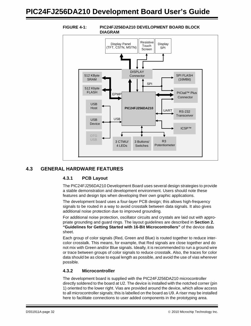
The development board is centered on the PIC24FJ256DA210 microcontroller which integrates in a single package a graphic controller, a CTMU for touch-sensing applica-tions, and a wide range of other peripherals.
The microcontroller’s Graphics module is capable of driving TFT, CSTN and MSTN dis-plays in a number of sizes and color depths. Many display applications (up to 8 bpp in QVGA) can be run from the microcontroller’s 96 KByte RAM buffer. For bigger displays or higher color resolution, the microcontroller can directly interface with external RAM devices for additional data storage. For non-volatile data storage, both serial and parallel Flash memory devices are provided.
The built-in USB functionality can be configured to operate in Device mode, as a stand-alone USB host, or as a USB On-The-Go (OTG) device. Host and OTG modes can be additionally configured for different types of bus sensing and external regulator support.
Push buttons, CTMU touch sensors and a potentiometer are provided for a variety of user-defined inputs. These share three common I/Os on the microcontroller, along with three LEDs, and are configured manually with jumpers.
A PICtail Plus edge connector is provided, allowing the development board to be used with different compatible PICtail Plus daughter board. An RS-232 port is provided for general purpose serial communications between the development board and a host PC; this serial port can also be re-configured to be available through the PICtail Plus connector.
Figure 4-1 shows the main components of the development board.
2010 Microchip Technology Inc. DS51911A-page 31
PIC24FJ256DA210 Development Board User’s Guide
FIGURE 4-1: PIC24FJ256DA210 DEVELOPMENT BOARD BLOCK DIAGRAM
4.3 GENERAL HARDWARE FEATURES
4.3.1 PCB Layout
The PIC24FJ256DA210 Development Board uses several design strategies to provide a stable demonstration and development environment. Users should note these features and design tips when developing their own graphic applications.
The development board uses a four-layer PCB design; this allows high-frequency signals to be routed in a way to avoid crosstalk between data signals. It also gives additional noise protection due to improved grounding.
For additional noise protection, oscillator circuits and crystals are laid out with appro-priate grounding and guard rings. The layout guidelines are described in Section 2. “Guidelines for Getting Started with 16-Bit Microcontrollers” of the device data sheet.
Each group of color signals (Red, Green and Blue) is routed together to reduce inter-color crosstalk. This means, for example, that Red signals are close together and do not mix with Green and/or Blue signals. Ideally, it is recommended to run a ground wire or trace between groups of color signals to reduce crosstalk. Also, the traces for color data should be as close to equal length as possible, and avoid the use of vias wherever possible.
4.3.2 Microcontroller
The development board is supplied with the PIC24FJ256DA210 microcontroller directly soldered to the board at U2. The device is installed with the notched corner (pin 1) oriented to the lower right. Vias are provided around the device, which allow access to all microcontroller signals; this is labelled on the board as U9. A riser may be installed here to facilitate connections to user added components in the prototyping area.
PIC24FJ256DA210
DISPLAY Connector
Display Panel(TFT, CSTN, MSTN)
512 KByte SRAM
512 Kbyte FLASH
OTG USB
USB Device
3 Buttons/Switches
USB Host
PICtail™ PlusEPMP
ResistiveTouch Screen
Display SPI
SPI
RS-232 Transceiver
UART
SPI FLASH(16MBit)
USB
ICSP™
R33 CTMU/ 4 LEDs
Connector
Potentiometer
DS51911A-page 32 2010 Microchip Technology Inc.

Development Board Hardware
4.3.3 Oscillator Options
The PIC24FJ256DA210 Development Board is equipped with two separate oscillator circuits. The main oscillator uses an 8 MHz crystal (Y1) and functions as the controller’s primary oscillator.
A second oscillator is implemented using a discrete oscillator circuit with a 32.768 kHz (watch type) crystal (Y2). This is connected to the microcontroller’s SCLKI pin, provid-ing an external clock source for the secondary oscillator option used to clock the RTCC and Timer1 modules. A discrete oscillator is used in this application to free up an addi-tional pin for general I/O use. To use this clock source, the microcontroller must be con-figured to use External Clock mode for the secondary oscillator. For additional information on secondary oscillator configuration, refer to the “PIC24FJ256DA210 Family Data Sheet” (DS39969).
4.3.4 Power Supply
The PIC24FJ256DA210 Development Board supports two power options.
In the first, an unregulated DC supply of 9V to 15V is supplied to J1. (A power supply is not provided with the development board, unless the kit was purchased. If one is required, Microchip Part number AC162039 is recommended). The 5V and 3.3V regulators (Q1 and Q2, respectively) provide stable power to the board, as well as compatible display daughter boards. Regulated 3.3V voltage is derived from the 5V regulated voltage.
Optionally, an external, regulated DC power supply can be used to provide power to the board. Two separate voltages are required: +5V (to TP3, the red terminal near the upper left corner, adjacent to J9) and +3.3V (to TP4, the yellow terminal near the upper right corner, adjacent to the prototype area).
The on-board voltage regulators can deliver a total combined current of 800 mA. If a larger display with a current rating higher than 800 mA (combined board and display rating) is to be used, the display board must be independently powered. In these cases, power to the display cannot be provided through display connector V1. Only common ground between the development board and the larger display should be connected through V1.
A green power-on LED (D6) indicates when power is applied to the board from either source. The power-on LED indicates the presence of +3.3V.
4.3.5 Programming and Debugging Interface
The PIC24FJ256DA210 Development Board can be programmed using either the (PICkit) connector (J9) or the 5-wire, RJ-11 (ICD) connector (J10). Only one interface may be used at any given time.
Use J9 to connect a PICkit 3 programmer, or other similar programmer/debugger devices, to program the development board. Use J10 to program the board using the MPLAB ICD 3 debugger or MPLAB REAL ICE in-circuit emulator.
4.3.6 Reset Switch (S4)
Switch S4 is connected to the MCLR line of the microcontroller. When pressed, it pulls the MCLR pin low, resetting the microcontroller (and any application the microcontroller is running). The same reset signal is also connected to the Reset signals of the PICkit and ICD connectors. However, any applications being run on PICtail daughter cards installed in the PICtail Plus port will not be automatically reset. In these cases, the user must provide an alternate hardware signal to the daughter board.
2010 Microchip Technology Inc. DS51911A-page 33
PIC24FJ256DA210 Development Board User’s Guide
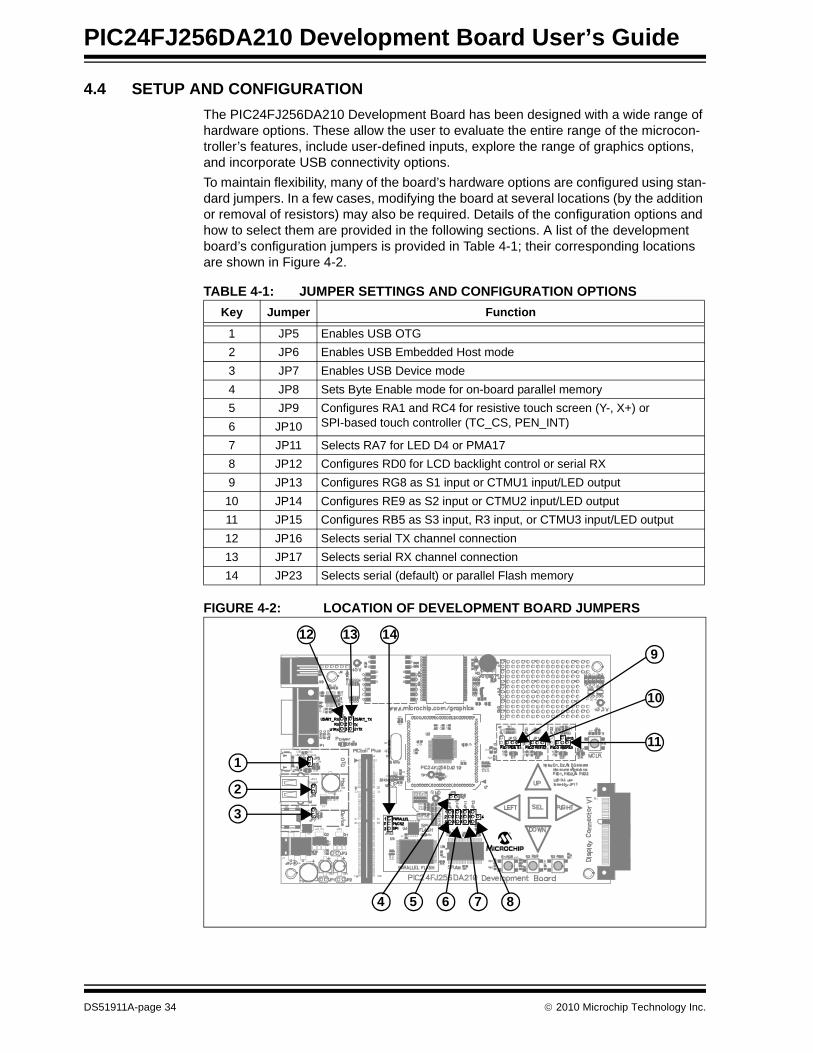
4.4 SETUP AND CONFIGURATION
The PIC24FJ256DA210 Development Board has been designed with a wide range of hardware options. These allow the user to evaluate the entire range of the microcon-troller’s features, include user-defined inputs, explore the range of graphics options, and incorporate USB connectivity options.
To maintain flexibility, many of the board’s hardware options are configured using stan-dard jumpers. In a few cases, modifying the board at several locations (by the addition or removal of resistors) may also be required. Details of the configuration options and how to select them are provided in the following sections. A list of the development board’s configuration jumpers is provided in Table 4-1; their corresponding locations are shown in Figure 4-2.
FIGURE 4-2: LOCATION OF DEVELOPMENT BOARD JUMPERS
TABLE 4-1: JUMPER SETTINGS AND CONFIGURATION OPTIONS
Key Jumper Function
1 JP5 Enables USB OTG
2 JP6 Enables USB Embedded Host mode
3 JP7 Enables USB Device mode
4 JP8 Sets Byte Enable mode for on-board parallel memory
5 JP9 Configures RA1 and RC4 for resistive touch screen (Y-, X+) or SPI-based touch controller (TC_CS, PEN_INT)6 JP10
7 JP11 Selects RA7 for LED D4 or PMA17
8 JP12 Configures RD0 for LCD backlight control or serial RX
9 JP13 Configures RG8 as S1 input or CTMU1 input/LED output
10 JP14 Configures RE9 as S2 input or CTMU2 input/LED output
11 JP15 Configures RB5 as S3 input, R3 input, or CTMU3 input/LED output
12 JP16 Selects serial TX channel connection
13 JP17 Selects serial RX channel connection
14 JP23 Selects serial (default) or parallel Flash memory
M
1
12
2
3
4 5 6 7 8
10
11
13 14
9
DS51911A-page 34 2010 Microchip Technology Inc.

Development Board Hardware
Due to pin constraints, some features of the development board overlap more than oth-ers. In these cases, configuring the board for one major functionality means limiting or disabling another. Table 4-2 shows the major areas of overlap. Additional details are provided in the following sections.
4.4.1 User-Defined Inputs and LEDs
The PIC24FJ256DA210 Development Board implements a variety of user-defined inputs: push button switches, capacitance-sensing touch pads, a potentiometer, and four LEDs. The development board multiplexes the switches, touch sensors, potenti-ometer and three of the LEDs through three I/O pins (RB5, RE9 and RG8). For each of these pins, only one input mode can be chosen at any given time. The fourth LED (D4) shares a pin with an address line for the external memory devices.
Note that the implementation of shared inputs and outputs used in the development board is not a recommended design practice. In this case, it is implemented in consid-eration of I/O pin constraints. Using separate pins for different input and output features is always recommended.
If the CTMU touch sensors are enabled, the LEDs can be used simultaneously. How-ever, care must be taken in the application to switch the I/O pins alternately as analog input and digital output as required. Please refer to the “PIC24FJ256DA210 Family Data Sheet” (DS39969) for details on configuring the I/O ports.
The user-defined features are configured using jumpers J13, J14 and J15. In some cases, modifications to accompanying resistors are also required. The locations of the components are shown in Figure 4-3. A summary of the jumper settings is provided in Table 4-3.
TABLE 4-2: SUMMARY OF BOARD CONFIGURATIONS VS. AVAILABILITY OF SPECIFIC FEATURES
Individual FeatureBoard Configuration Options
No CTMU CTMU USB OTG PICtail™ Plus Options
Flash and SRAM access modes
Byte and Word
Byte and Word
Byte and Word
Word only(1)
Parallel Flash/SPI Flash Memory
512 Kbytes/2 Mbit
512 Kbytes/2 Mbit
512 Kbytes/2 Mbit
256 Kbytes/N.A.
SRAM 512 Kbytes 512 Kbytes 512 Kbytes 256 Kbytes
Resistive TouchscreenOR Touch SPI channel
Y Y Y Y
Potentiometer Y N N Y
Touch pads (CTMU) N Y(2) N N
User-defined Buttons Y N N Y(2)
User-defined LEDs N Y(3) N 1
UART Channels 1 1 1 1
USB Modes Host or Device
Host or Device
OTG only Host or Device
PICtail Plus Expansion N Y(3) N Y
Note 1: The only display mode available in this configuration is 16 bpp.
2: CTMU channels and push buttons are available with certain PICtail™ Daughter Boards only. The number of inputs available depends on the daughter board and the application. See Section 4.4.6 “PICtail™ Plus Card Modular Expansion Connector” for additional information.
3: LED outputs are shared with CTMU input channels.
2010 Microchip Technology Inc. DS51911A-page 35

PIC24FJ256DA210 Development Board User’s Guide
FIGURE 4-3: CONFIGURATION OF USER-DEFINED FEATURES
TABLE 4-3: JUMPER SETTINGS FOR RB5, RE9 AND RG8 INPUTS
4.4.1.1 USER-DEFINED PUSH BUTTONS (S1, S2 AND S3)
The development board comes with three general purpose switches, S1, S2 and S3, for user inputs. The push button switches are normally pulled up to VDD when unpressed, and pulled to ground when pressed.
To enable the switches:
1. To enable switch S1 (Figure 4-3, callout 1):
a) Set jumper JP13 to bridge RG8-S1 (default).
b) Populate resistor R25 with a 0 resistor (default)
c) If installed, remove resistors R26 and R27 (not populated by default)
2. To enable switch S2 (Figure 4-3, callout 2):
a) Set jumper JP14 to bridge RE9-S2 (default)
b) Populate resistor R31 with a 0 resistor (default)
c) If installed, remove resistor R32 (not populated by default)
3. To enable switch S3 (Figure 4-3, callout 3):
a) Set jumper JP15 to bridge RB5-S3
b) Populate resistor R41 with a 0 resistor (default)
c) If installed, remove resistor R45 (not populated by default)
Jumper ConfigurationJumper Setting
JP13 RG8 is push button S1 input (default) RG8–S1
RG8 is CTMU Pad 1 input and LED D1 output PAD1–RG8
JP14 RE9 is push button S2 input (default) RE9–S2
RE9 is CTMU Pad 2 input and LED D2 output PAD2–RE9
JP15 RB5 is push button S3 input RB5–S3
RB5 is CTMU Pad 3 input and LED D3 output PAD3–RB5
RB5 is potentiometer (R3) input (default) RB5–POT
M
1 2 3
DS51911A-page 36 2010 Microchip Technology Inc.

Development Board Hardware
4.4.1.2 CTMU TOUCH SENSE INPUTS
The development board is equipped with five touch sensor inputs. These are multi-plexed between three CTMU (Charge Time Measurement Unit) analog channels, as shown in Table 4-4. The areas within the white border of each pad is the touch-sensitive areas. Note that all three CTMU inputs must be enabled to use the entire pad.
TABLE 4-4: CTMU TOUCH PAD COMBINATIONS
To enable the CTMU Touch Pads:
1. To enable PAD1 (Figure 4-3, callout 1):
a) Set jumper JP13 to position PAD1–RG8
b) If installed, remove resistors R26 and R27
c) Populate resistor R25 with a 0 resistor (default)
2. To enable PAD2 (Figure 4-3, callout 2):
a) Set jumper JP14 to position PAD2–RE9
b) If installed, remove resistor R32
c) Populate resistor R31 with a 0 resistor (default)
3. To enable PAD3 (Figure 4-3, callout 3):
a) Set jumper JP15 to position PAD3–RB5
b) If installed, remove resistor R45
c) Populate resistor R41 with a 0 resistor (default)
4.4.1.3 ANALOG INPUT (POTENTIOMETER)
Pin RB5 can also be configured to read potentiometer R3. This selection is enabled by setting JP15 to position RB5–POT. No other changes are required.
4.4.1.4 LED OUTPUTS
There are four user-defined LEDs on the development board.
LEDs D1, D2 and D3 (red) are multiplexed with the CTMU pads. They are individually enabled when their corresponding CTMU pads are enabled, as described in Section 4.4.1.2 “CTMU Touch Sense Inputs”.
LED D4 (red) is multiplexed with address line 17 of the parallel RAM and Flash mem-ories. To use this LED, jumper JP11 must be set to position 1-2. Refer to Section 4.4.5 “On-Board External Memory” for more information.
Touch Pad PAD1 (RG8) PAD2 (RE9) PAD3 (RB5)
LEFT X X
RIGHT X X
UP X
DOWN X
SEL X X
Note: CTMU signals are connected to PIC24FJ256DA210 analog pins. Make sure that the pins are set to analog pins using their corresponding ANSx control bits. Refer to the “PIC24FJ256DA210 Family Data Sheet (DS39969)” for details.
2010 Microchip Technology Inc. DS51911A-page 37
PIC24FJ256DA210 Development Board User’s Guide
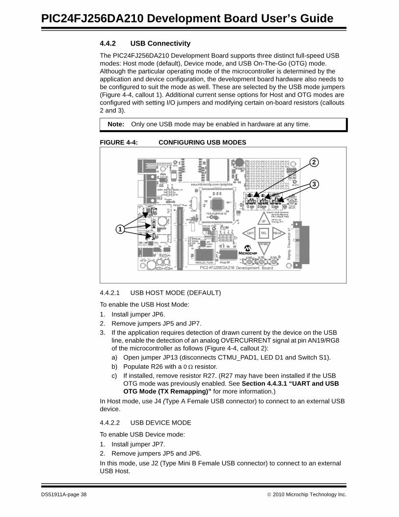
4.4.2 USB Connectivity
The PIC24FJ256DA210 Development Board supports three distinct full-speed USB modes: Host mode (default), Device mode, and USB On-The-Go (OTG) mode. Although the particular operating mode of the microcontroller is determined by the application and device configuration, the development board hardware also needs to be configured to suit the mode as well. These are selected by the USB mode jumpers (Figure 4-4, callout 1). Additional current sense options for Host and OTG modes are configured with setting I/O jumpers and modifying certain on-board resistors (callouts 2 and 3).
FIGURE 4-4: CONFIGURING USB MODES
4.4.2.1 USB HOST MODE (DEFAULT)
To enable the USB Host Mode:
1. Install jumper JP6.
2. Remove jumpers JP5 and JP7.
3. If the application requires detection of drawn current by the device on the USB line, enable the detection of an analog OVERCURRENT signal at pin AN19/RG8 of the microcontroller as follows (Figure 4-4, callout 2):
a) Open jumper JP13 (disconnects CTMU_PAD1, LED D1 and Switch S1).
b) Populate R26 with a 0 resistor.
c) If installed, remove resistor R27. (R27 may have been installed if the USB OTG mode was previously enabled. See Section 4.4.3.1 “UART and USB OTG Mode (TX Remapping)” for more information.)
In Host mode, use J4 (Type A Female USB connector) to connect to an external USB device.
4.4.2.2 USB DEVICE MODE
To enable USB Device mode:
1. Install jumper JP7.
2. Remove jumpers JP5 and JP6.
In this mode, use J2 (Type Mini B Female USB connector) to connect to an external USB Host.
Note: Only one USB mode may be enabled in hardware at any time.
M
1
2
3
DS51911A-page 38 2010 Microchip Technology Inc.

Development Board Hardware
4.4.2.3 USB ON-THE-GO (OTG) MODE
To enable the USB OTG mode:
1. Install jumper J5.
2. Remove jumpers J6 and J7.
3. To detect the status of the regulated output voltage of the charge pump, connect the charge pump PGOOD signal to the microcontroller (Figure 4-4, callout 3):
a) Remove jumper JP14 (disconnects CTMU_PAD2, LED D2 and switch S2).
b) Populate resistor R32 with a 0resistor (connects PGOOD signal to pin AN21/RE9).
4. To have software control of the charge pump, connect the SHDN signal to the microcontroller (Figure 4-4, callout 3):
a) Remove jumper JP15 (disconnects the potentiometer, switch S3, CTMU_PAD3 and LED D3).
b) Populate resistor R45 with a 0 resistor.
In USB OTG mode, use J7 (Type Micro AB Female USB connector) to connect with external USB OTG devices.
4.4.3 UART (RS-232)
The development board provides one UART, with its RX and TX signals appearing on pins RD0 and RF3 of the PIC24FJ256DA210, respectively. The signals can be configured to appear at one of two places:
• The RS-232 external serial port (default).
• The PICtail Plus connector, as signals U1RX (pin 2) and U1TX (pin 4).
An RS-232 level shifter (U3) has been provided with all necessary hardware to support the external serial port. The DB-9F serial connector (P1) is wired to support hardware flow control; however, the flow control signals are not connected to the microcontroller. The port is configured as a Data Communication Equipment (DCE) device.
The UART’s availability is configured by jumpers JP16 and JP17. Their location is shown in Figure 4-5.
To access the UART through the RS-232 serial port:
1. Set jumper J16 to position 1-2 (USART_TX – TX) (default).
2. Set jumper J17 to position 1-2 (USART_RX – RX) (default).
In this configuration, a host PC running the appropriate application can communicate with the development board using the serial channel. Use a standard (“straight-through”) serial cable connected to P1.
To access the UART through the PICtail Plus expansion port:
1. Set jumper J16 to position 2-3 (U1TX – TX).
2. Set jumper J17 to position 2-3 (U1RX – RX).
In this configuration, the U1RX and U1TX signals appear at pins 2 and 4 of the PICtail Plus connector, respectively.
Note: Enabling USB OTG mode may require the remapping of the UART’s TX signal. See Section 4.4.3.1 “UART and USB OTG Mode (TX Remap-ping)” for more information.
Note: The TX and RX signals are mapped to the microcontroller pins using the Peripheral Pin Select (PPS) feature. When developing applications, make sure that the pins are remapped properly to use the UART Receive and UART Transmit signals. Refer to Section 10.4 “Peripheral Pin Select” of the PIC24FJ256DA210 data sheet for a detailed discussion of PPS.
2010 Microchip Technology Inc. DS51911A-page 39

PIC24FJ256DA210 Development Board User’s Guide
FIGURE 4-5: UART CONFIGURATION
4.4.3.1 UART AND USB OTG MODE (TX REMAPPING)
Normally, the UART TX signal appears on pin RF3, along with the USBID signal. When USB OTG mode is enabled, USBID takes priority over the TX signal. If the UART is also needed, this requires the TX signal to be remapped to another pin. The development board allows for RG8, normally used for S1/PAD1/LED1, to function as the TX signal in these cases. In addition to remapping the pin in software using PPS, resistor R4, R5, R26 and R27 will also need to be changed (Figure 4-6).
To remap the TX signal with USB OTG enabled:
1. If populated, remove resistor R4 (callout 1). Alternatively, remove jumper JP13 (callout 2). (Both disconnect the TX signal from pin RF3.)
2. Populate resistor R5 (callout 1) with a 0 resistor (connects USBID signal to pin RF3).
3. Populate resistor R27 with a 0 resistor (callout 2) (connects TX signal to pin RG8).
4. If populated, remove resistor R26 (callout 2) (disconnects Overcurrent Sense signal).
FIGURE 4-6: REMAPPING THE UART TX SIGNAL
M
M
12
DS51911A-page 40 2010 Microchip Technology Inc.

Development Board Hardware
4.4.3.2 UART AND DISPLAY BACKLIGHT (RX SIGNAL)
The UART’s RX signal is mapped to only one pin (RD0) of the microcontroller. This pin is also used by the development board to optionally control the backlight for the display daughter board; all functions are multiplexed through the same jumper, JP12. If either of the backlight control options is selected, the UART becomes unavailable to the exter-nal RS-232 port.
4.4.4 Graphics Port
The PIC24FJ256DA210 Development Board can support TFT, MSTN and CSTN displays. Displays of 4, 8 and 16-bit data widths are supported. The 64-pin display Con-nector V1 (J3) (on the right hand side bottom corner of the board) is provided for con-nection of Microchip display boards.
4.4.4.1 TFT AND STN INTERFACES
When developing applications using TFT displays and the Graphics Display Prototype Board, the 16-bit display bus can be used to send 16-bit RGB data (5-6-5 bits respec-tively) to a standard 24-bit (8-8-8) or 18-bit (6-6-6) RGB display. To do this, color data from the microcontroller is mapped to the Most Significant bits (MSbs) of the display. The Least Significant bit lines of the display (3-2-3 for 24-bit displays, 1-0-1 for 18-bit) are then tied to the MSb. This technique allows full brightness whenever the MSb is ‘1’, and full blackness when the MSb is ‘0’. The controller-to-display data mapping is detailed in Table 4-5.
TABLE 4-5: RGB INTERFACE MAPPING FOR TFT DISPLAYS
4.4.4.2 STN INTERFACES
The development board can directly interface with STN displays (both CSTN and MSTN) of 4, 8 or 16-bit data width. The mapping of graphics data to the display data input is described in Table 4-6. Configuration of the different data widths is done by the graphics controller module through the register interface. Refer to the “PIC24FJ256DA210 Family Data Sheet” (DS39969) for more information.
TABLE 4-6: STN INTERFACE MAPPING
Graphics Data Pins (GDx)18-Bit RGB Display
(6-6-6)24-Bit RGB Display
(8-8-8)
RED
GD<15:11> Red<5:1> Red<7:3>
GD<15> Red<0> Red<2:0>
GREEN
GD<10:5> Green<5:0> Green<7:2>
GD<10> Green<5> Green<1:0>
BLUE
GD<4:0> Blue<5:1> Blue<7:3>
GD<4> Blue<0> Blue<2:0>
Graphics Data Pins (GDx) 4-bit 8-bit 16-bit
GD<3:0> M<3:0> M<3:0> M<3:0>
GD<7:4> Unused M<7:4> M<7:4>
GD<15:8> Unused Unused M<15:8>
2010 Microchip Technology Inc. DS51911A-page 41

PIC24FJ256DA210 Development Board User’s Guide
4.4.4.3 RESISTIVE TOUCH SCREEN INTERFACE
The development board supports display panels with a built-in 4-wire resistive touch screen. The resistive touch screen interface (X-, Y-, X+ and Y+) is used to directly con-nect to the touch screen signals. X+ and Y+ are both analog and digital signals, and are connected to I/O ports that can function both as analog inputs and digital outputs. X- and Y- are digital output signals only, and are connected to digital I/O ports. The X+ and Y- signals are multiplexed with the SPI based touch screen controller.
When using the 4-wire resistive touch screen interface, jumpers JP9 and JP10 must be set to their default positions, bridging pins 1 and 2 (Figure 4-7, callout 1).
4.4.4.4 SPI TOUCH CONTROLLER INTERFACE
Two SPI channels (two Chip Select lines) are provided in Display Connector V1 to support display panels equipped with the following:
• SPI-Based Timing Controller: Some displays requires programming of an on-board Timing Controller (TCON) to initialize the settings of the display before it is used. The TCON is used to synchronize the display glass timing with the dis-play controller signal timing. This option is provided on the pins A27 (SPI_SCK), A28 (SPI_MISO), B27 (DISP_SPI_CS) and B28 (SPI_MOSI) of display connector V1.
• SPI-Based Touch Controller: In some cases, an SPI-based touch module is used with the display. Every time a touch is detected, it sends an interrupt to the host controller to inform the host that there is a fresh touch input and the information must be forwarded from the touch module to the host controller through SPI com-munications. The development board shares two of the pins of the 4-wire resistive touch screen with the interrupt and chip select line of the SPI based touch control-ler. The sharing is done this way since in any system, only one of the two types of user interface will be used.
The SPI-based touch control features are configured by jumpers JP9 and JP10 (Figure 4-7, callout 1). To enable the use of an SPI-based touch controller, set jumpers JP9 and JP10 to bridge positions 2-3.
FIGURE 4-7: TOUCH CONTROLLER AND BACKLIGHT CONFIGURATION
Note: As of this writing, none of the Microchip display boards support SPI-based touch controllers.
M
1 2
DS51911A-page 42 2010 Microchip Technology Inc.

Development Board Hardware
4.4.4.5 BACKLIGHT CONTROL
Depending on the display glass being used, backlight control is provided as an ON/OFF signal, or as a PWM pulse train for a continuous range of brightness. Jumper JP12 (Figure 4-7, callout 2) selects which signal is enabled on display connector V1. By default, backlight control is disconnected (position 2-4).
• To enable BKLT_EN (ON/OFF), set JP12 to bridge 2-3.
• To enable BKLT_PWM (PWM controlled contrast), set JP12 to bridge 1-2.
4.4.5 On-Board External Memory
The PIC24FJ256DA210 can be used to create a graphics solution without any external memory resources. However, in cases where the application requires a higher color depth (8 bits per pixel or more), or larger storage for images and data, external SRAM and Flash memory devices are provided on the development board.
Both SRAM and parallel Flash memory can be enabled at the same time. The Enhanced Parallel Master Port module (EPMP) accesses memory on both devices with the same data and address lines. PMCS1 is used as the Chip Select signal for the SRAM, and PMCS2 is used for the parallel Flash. Note, however, that configuring a memory addressing size option for one device selects the same size for the other.
If all 19 address lines of the EPMP are not required, PMA17 and PMA18 can be con-figured for other purposes. PMA17 can be used to control LED D4, while PMA18 can be reconfigured to function as an I/O on the PICtail Plus Expansion port.
For more information on using the EPMP, refer to “Enhanced Parallel Master Port (EPMP)” (DS39730) for more information.
4.4.5.1 EXTERNAL SRAM
The PIC24FJ256DA210 Development Board is provided with 512 Kbyte of external SRAM, populating U6. By default, only 256 out of the 512 KByte is enabled; this allows PMA17 to control LED D4 in the default board default configuration. If required, the SRAM may be upgraded to 1 MByte by replacing U6 with a different device. The SRAM interfaces with the microcontroller through the EPMP interface. Use of external SRAM is optional if internal 24/96 Kbyte RAM of PIC24FJ256DA210 cannot accommodate the required frame buffer size for a specific color depth and resolution combination.
SRAM access time is an important aspect of the interface to the EPMP port. In most QVGA based applications, the use of a 55 ns access time is enough to meet the refresh requirements of the display. The use of a 10 ns access time SRAM on the board is due to the fact that VGA resolution display, which requires more bandwidth, can also be driven by the development board.
The SRAM can be configured for one of three memory address ranges, shown in Table 4-7.
TABLE 4-7: SRAM MEMORY OPTIONS
Note: If either of the backlight control modes is selected, access to the UART will be disabled. See Section 4.4.3.2 “UART and Display Backlight (RX Signal)” for more information.
Size JP11 R63Active EPMP
Address Lines
Recommended Part #s
256 Kbyte (default)
Open Open PMA<16:0> IS61LV25616AL-10TLIDT71V416SAS7C34098A512 Kbyte Bridged Open PMA<17:0>
1 Mbyte Bridged 0 PMA<18:0> IS61WV51216BLL-10TLI
2010 Microchip Technology Inc. DS51911A-page 43
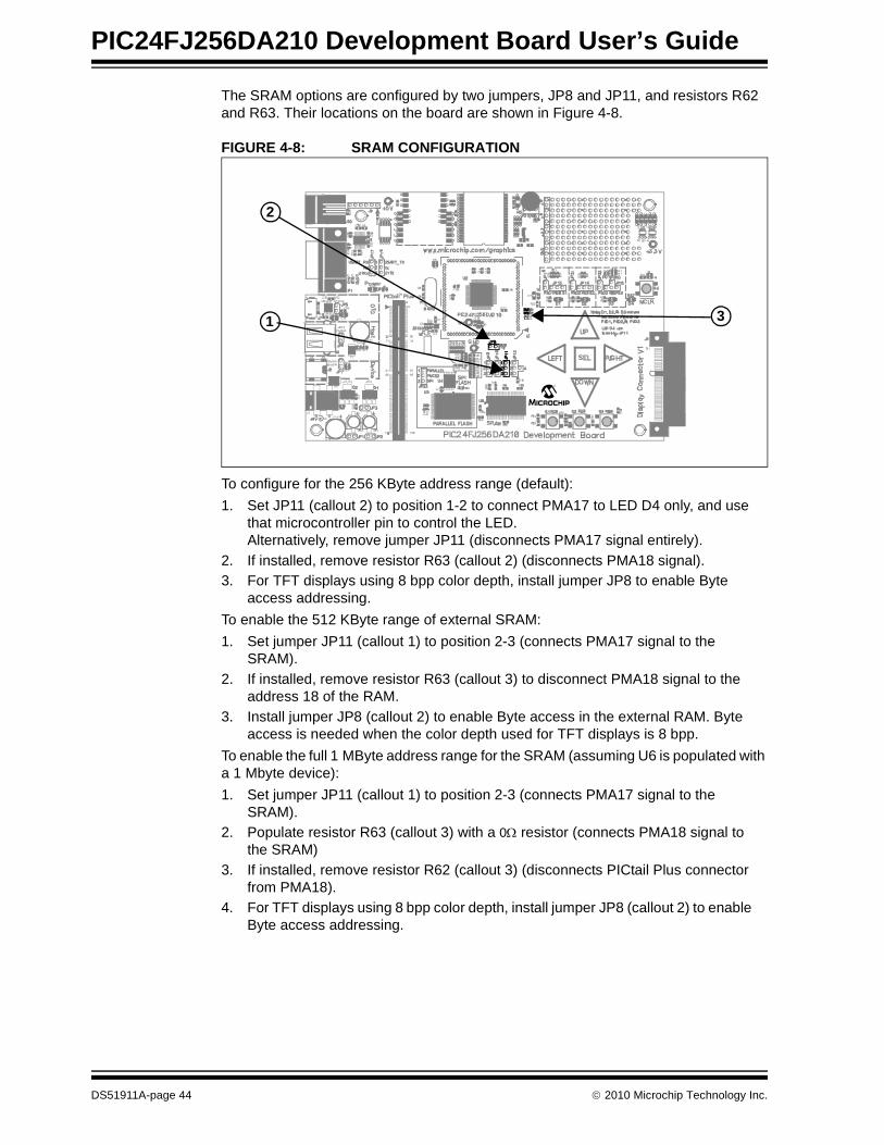
PIC24FJ256DA210 Development Board User’s Guide
The SRAM options are configured by two jumpers, JP8 and JP11, and resistors R62 and R63. Their locations on the board are shown in Figure 4-8.
FIGURE 4-8: SRAM CONFIGURATION
To configure for the 256 KByte address range (default):
1. Set JP11 (callout 2) to position 1-2 to connect PMA17 to LED D4 only, and use that microcontroller pin to control the LED.Alternatively, remove jumper JP11 (disconnects PMA17 signal entirely).
2. If installed, remove resistor R63 (callout 2) (disconnects PMA18 signal).
3. For TFT displays using 8 bpp color depth, install jumper JP8 to enable Byte access addressing.
To enable the 512 KByte range of external SRAM:
1. Set jumper JP11 (callout 1) to position 2-3 (connects PMA17 signal to the SRAM).
2. If installed, remove resistor R63 (callout 3) to disconnect PMA18 signal to the address 18 of the RAM.
3. Install jumper JP8 (callout 2) to enable Byte access in the external RAM. Byte access is needed when the color depth used for TFT displays is 8 bpp.
To enable the full 1 MByte address range for the SRAM (assuming U6 is populated with a 1 Mbyte device):
1. Set jumper JP11 (callout 1) to position 2-3 (connects PMA17 signal to the SRAM).
2. Populate resistor R63 (callout 3) with a 0 resistor (connects PMA18 signal to the SRAM)
3. If installed, remove resistor R62 (callout 3) (disconnects PICtail Plus connector from PMA18).
4. For TFT displays using 8 bpp color depth, install jumper JP8 (callout 2) to enable Byte access addressing.
M
1
2
3
DS51911A-page 44 2010 Microchip Technology Inc.

Development Board Hardware
4.4.5.2 EXTERNAL FLASH MEMORY
The PIC24FJ256DA210 Development Board has two external Flash memory devices. Selection is controlled by jumper JP23. Only one can be enabled at any given time:
• 512 Kbyte Parallel Flash (SST39LF400A), connected to the EPMP port.
• 16 Mbits (2 Mbyte) SPI Serial Flash (SST25VF016B).
Flash memory configuration uses the same jumpers and resistors as SRAM configura-tion (Figure 4-9). An additional jumper, JP23 (callout 1), selects between the serial and parallel devices.
FIGURE 4-9: FLASH MEMORY CONFIGURATION
4.4.5.2.1 Serial Flash Memory
To use the SPI Flash memory, set jumper JP23 to bridge pins 2 and 3 (PMCS2 – SPI). The microcontroller’s SPI module is used to communicate with the memory device; the PMCS2 signal is used as the Chip Select signal .
4.4.5.2.2 Parallel Flash Memory
Like the SRAM, the on-board parallel Flash memory can be configured to use one of three memory address ranges (shown in Table 4-8).
TABLE 4-8: PARALLEL FLASH MEMORY RANGES
Size JP11 R63Active EPMP
Address Lines
Recommended Part #
256 Kbyte (default)
Open Open PMA<16:0>
SST39LF400A-55-4C-EKE512 Kbyte Bridged Open PMA<17:0>
1 Mbyte Bridged 0 PMA<18:0> SST39VF800A-70-4C-EKE
M
2 3
4
1
2010 Microchip Technology Inc. DS51911A-page 45

PIC24FJ256DA210 Development Board User’s Guide
To configure the 256 KByte address range (default):
1. Set jumper JP23 (callout 1) to position 1-2 (enables the parallel Flash memory).
2. Set JP11 (callout 2) to position 1-2 to connect PMA17 to LED D4 only, and use that microcontroller pin to control the LED.Alternatively, remove jumper JP11 (disconnects PMA17 signal entirely).
3. If installed, remove resistor R63 (callout 4) (disconnects PMA18 signal from Flash memory).
To configure the 512 KByte address range:
1. Set jumper JP23 (callout 1) to position 1-2 (enables parallel Flash memory).
2. Set jumper JP11 (callout 2) to position 2-3 (connects PMA17 signal to Flash memory).
3. If installed, remove resistor R63 (callout 4) (disconnects PMA18 signal from Flash memory).
To configure the 1024 KByte address range (assuming U5 is populated with a 1 Mbyte device):
1. Set jumper JP23 to position 1-2 (callout 1) (enables parallel Flash memory).
2. Set jumper JP11 (callout 2) position 2-3 (connects PMA17 signal to Flash memory).
3. Populate resistor R63 (callout 4) with a 0 resistor (connects PMA18 signal to Flash memory).
4. If installed, remove resistor R62 (callout 4) (disconnects PMA18 from the PICtail Plus expansion port).
4.4.6 PICtail™ Plus Card Modular Expansion Connector
A 120-pin PICtail Plus connector (J8) is provided on the PIC24FJ256DA210 Develop-ment Board for expansion and integration of other solutions. At the time of this writing, the following daughter boards are supported on the PIC24FJ256DA210 Development Board:
• PICtail Daughter Board for SD & MMC Cards (AC164122)
• Ethernet PICtail Plus Daughter Board (AC164123)
• Fast 100 Mbps Ethernet PICtail Plus Daughter Board (AC164132)
• MRF24WB0MA PICtail Plus Daughter Board (AC164136-4)
• MRF49XA PICtail Plus Daughter Board (AC164137-1 or AC164137-2)
• Speech Playback PICtail Plus Daughter Board (AC164125)
• IrDA® PICtail Plus Daughter Board (AC164124)
Additional boards are planned to be available in the future. Users are encouraged to check the Microchip web site periodically for more information.
To enable the support of multiple PICtail Plus Daughter Boards, the development board maps selected I/Os to multiple PICtail Plus pins. In some cases, using certain daughter boards may mean disabling some functionality on the development board. In general, when the PICtail Plus connector is in use, these development board features are not available:
1. All CTMU channels (most daughter boards).
2. EPMP Address lines PMA18 and PMA17. This reduces the accessible area of the parallel Flash device to 256 Kbytes, regardless of the device installed
3. PMP Byte Enable line PMBE1. This limits parallel Flash and SRAM devices to Word accesses; in turn, this limits display modes to 16 bpp mode.
4. USB OTG functionality (Device and Host modes are still available)
DS51911A-page 46 2010 Microchip Technology Inc.

Development Board Hardware
4.4.6.1 DAUGHTER BOARD-SPECIFIC HARDWARE MODIFICATIONS
Depending on the PICtail Plus Daughter Board to be used, hardware modification to the development board may be required. The modifications re-route different signals from the microcontroller, particularly EPMP signals, to different pins of the connector. All changes consist of placing 0 resistors in designated areas to enable the connec-tions, or removing existing resistors in other places to disable existing connections. All of the resistors are located in a single group adjacent to the Flash memory area, shown in Figure 4-10. They are also shown as a single group in Figure A-6 of the development board schematic.
FIGURE 4-10: LOCATION OF CONFIGURATION RESISTORS
For additional information on the configuration resistors, as well as specific modifica-tions for particular daughter boards, please refer to Appendix B. “Modifications for PICtail Plus Daughter Boards”.
4.4.7 Current Measurement
To provide additional information on developing hardware solutions, the development board includes current measurement points at three locations. These permit the current drawn by the different branches of the development board to be measured separately.
The measurement points are unpopulated jumpers at JP1, JP2 and JP3 (Figure 4-11, callouts 1,2 and 3, respectively). To measure current, cut the trace on the reverse side of the board that shorts the two vias for the jumper, then insert the current measuring device between the two vias.
JP3 can be used to measure the total current drawn by the board from the 9V power supply. JP1 can be used to measure the total current (at 3.3V) drawn by the microcon-troller, and JP2 can be used to measure the total current drawn by the remaining 3.3V branch of the board. The current drawn by the 5V branch can be measured by subtract-ing the sum of the currents of JP1 and JP2 from the total current measured at JP3.
M
2010 Microchip Technology Inc. DS51911A-page 47

PIC24FJ256DA210 Development Board User’s Guide
FIGURE 4-11: CURRENT MEASUREMENT LOCATIONS
4.4.8 Other Considerations
The PIC24FJ256DA210 supports two slightly different configuration options for its Enhanced PMP. The configurations are selected by the ALTPMP Configuration bit; this allows some flexibility in hardware design by remapping several address and Chip Select lines to different pins. Table 4-9 summarizes the differences.
The development board is designed with the assumption that the Enhanced PMP inter-face is in the alternate configuration (ALTPMP = 0). This allows the use of three addi-tional analog pins that would otherwise be used by the EPMP module. Users should keep this in mind when designing applications that will be used with the development board.
TABLE 4-9: PIN ASSIGNMENTS FOR ALTERNATE EPMP CONFIGURATIONS
Pin # Pin FunctionALTPMP
‘0’ ‘1’
10 AN17/C1IND/RP21/PMA5/PMA18/CN8/RG6 PMA18 PMA5
40 RPI32/PMA18/PMA5/CN75/RF12 PMA5 PMA18
59 SDA2/PMA20/PMA4/CN36/RA3 PMA4 PMA20
60 TDI/PMA21/PMA3/CN37/RA4 PMA3 PMA21
66 SCL1/RPI36/PMA22/PMCS2/CN43/RA14 PMCS2 PMA22
M3
1 2
DS51911A-page 48 2010 Microchip Technology Inc.

PIC24FJ256DA210DEVELOPMENT BOARD
USER’S GUIDE
Appendix A. Development Board Schematics
A.1 INTRODUCTION
This section provides detailed technical information on the PIC24FJ256DA210 Devel-opment Board. All information in this appendix refers to revision 1.1 of the development board.
A.2 HARDWARE FEATURES
TABLE A-1: CONNECTOR SUMMARY
Connector Description
J1 Unregulated 9V to 15V power supply connector (PJ-0029)
J2 USB Device Mode (Mini B type) Connector
J3 Microchip Display Connector
J4 USB Host Mode (Type A) Connector
J7 USB OTG Mode (Micro AB type) Connector
J8 PICtail™ Plus 120-pin Edge Connector for Daughter Board expansion
J9 PICkit™ Program and Debug connector (6-pin riser)
J10 ICD Program and Debug connector (RJ-11)
P1 RS-232 (DB-9F) Serial Connector
2010 Microchip Technology Inc. DS51911A-page 49

PIC24FJ256DA210 Development Board User’s Guide
TABLE A-2: SUMMARY OF ALL JUMPER SELECTIONS
Jumper Function Jumper Setting
JP5 Connect VBUS for USB OTG operation Bridged
USB OTG is not used (default) Open
JP6 Connect VBUS for USB Embedded Host operation (default) Bridged
Embedded USB Host operation is not used Open
JP7 Connect VBUS for USB Device operation Bridged
USB Device operation is not used (default) Open
JP8 Connect PMBE1 to Upper Byte signal of External RAM (U6) (default) Bridged
Open, PMBE1 can be used in PICtail™ Plus Expansion Port Open
JP9 Y- signal of resistive touch screen is connected to RA1 (default) 1-2
SPI touch screen signal TC_CS is connected to RA1 2-3
JP10 X+ signal of resistive touch screen is connected to RC4 (default) 1-2
SPI touch screen interrupt PEN_INT is connected to RC4 2-3
JP11 PMA17/RA7 signal is connected to LED D4 (default) 1-2
PMA17/RA7 signal is connected to memory address line 17 2-3
JP12 Backlight PWM controlled signal (BKLT_PWM) is connected to RD0 1-2
Backlight signal BKLT_EN is connected to RD0 2-3
Serial RX signal is connected to RD0 (default) 2-4
JP13 Switch S1 connected to AN19/RG8 (default) 1-2
CTMU PAD1 and LED D1 connected to AN19/RG8 2-3
JP14 Switch S2 connected to AN21/RE9 (default) 1-2
CTMU PAD2 and LED D2 connected to AN21/RE9 2-3
JP15 Switch S3 connected to AN5/RB5 (default) 1-2
CTMU PAD3 and LED D3 connected to AN5/RB5 2-3
Potentiometer POT R3 connected to AN5/RB5 2-4
JP16 Serial TX signal connected to USART_TX of RS-232 level shifter (default)
1-2
Serial TX signal connected to U1TX of PICtail Plus Port 2-3
JP17 Serial RX signal connected to USART_RX of RS-232 level shifter (default)
1-2
Serial RX signal connected to U1RX of PICtail Plus Port 2-3
JP23 PMCS2 signal connected to parallel Flash memory chip select 1-2
PMCS2 signal connected to SPI Flash memory chip select (default) 2-3
Legend: Bold text indicates jumper labelling on development board in the absence of numbering (JP13 through JP15).
DS51911A-page 50 2010 Microchip Technology Inc.
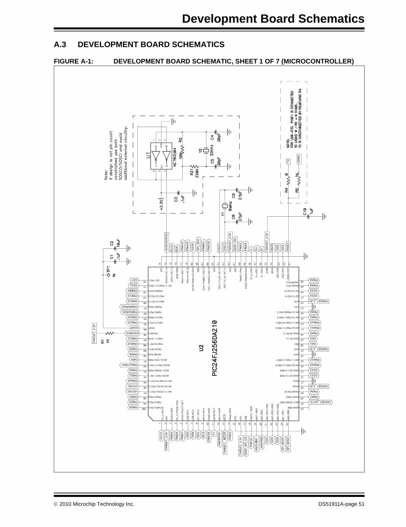
Development Board Schematics
A.3 DEVELOPMENT BOARD SCHEMATICS
FIGURE A-1: DEVELOPMENT BOARD SCHEMATIC, SHEET 1 OF 7 (MICROCONTROLLER)
PMD4
PMD3
HSYNC
VSYNC
PMD1
PMD0
GEN
PMD8
PMD10
PMD11
VCAP
PMD15
PMD12
PMBE0
GD7
PMA6
TARGET_3.3V
GD12
GD13
PMA12
RA1
GD2
PMA11
PMA10
PMA0PMRD/RD5
PMWR/RD4
GD14
GD15
PMA8
TARGET_DATA
SP
I_M
ISO
SP
I_M
OS
I
GD
5
GD
4
AN
21
/RE
9
PM
CS
1
TA
RGE
T_
3.3
V
GD
3
VB
US
D+
X-
RD
0
RC
13
US
BID
TX
GD
6
AN
5/R
B5
DIS
P_S
PI_
CS
PMD2
PMA16
PMD9
ENVREG
PMD14
PMD13
GD11
GD
9
D-
SO
SC
O/S
CK
I
PMA7
PMA13
TARGET_3.3V
PMA17/RA7
PMA5
PMA1
TARGET_3.3V
PMA9
TA
RGE
T_
MC
LR
AN
19/
RG
8
PM
A1
8
RC
4
GD
8
GD
0
PM
D6
PM
D5
GC
LK
PIN
51
TA
RG
ET
_3.
3V
PM
A3
DIS
P_O
N
OS
C1
OS
C2
PM
CS
2
PM
BE
1
GD
10
PM
A15
PM
A2
GD
1
Y+
PM
D7
TA
RGE
T_
3.3
V
TA
RG
ET
_3.3
V
PM
A4
TA
RG
ET
_3.
3V
SP
I_S
CK
PM
A14
2010 Microchip Technology Inc. DS51911A-page 51
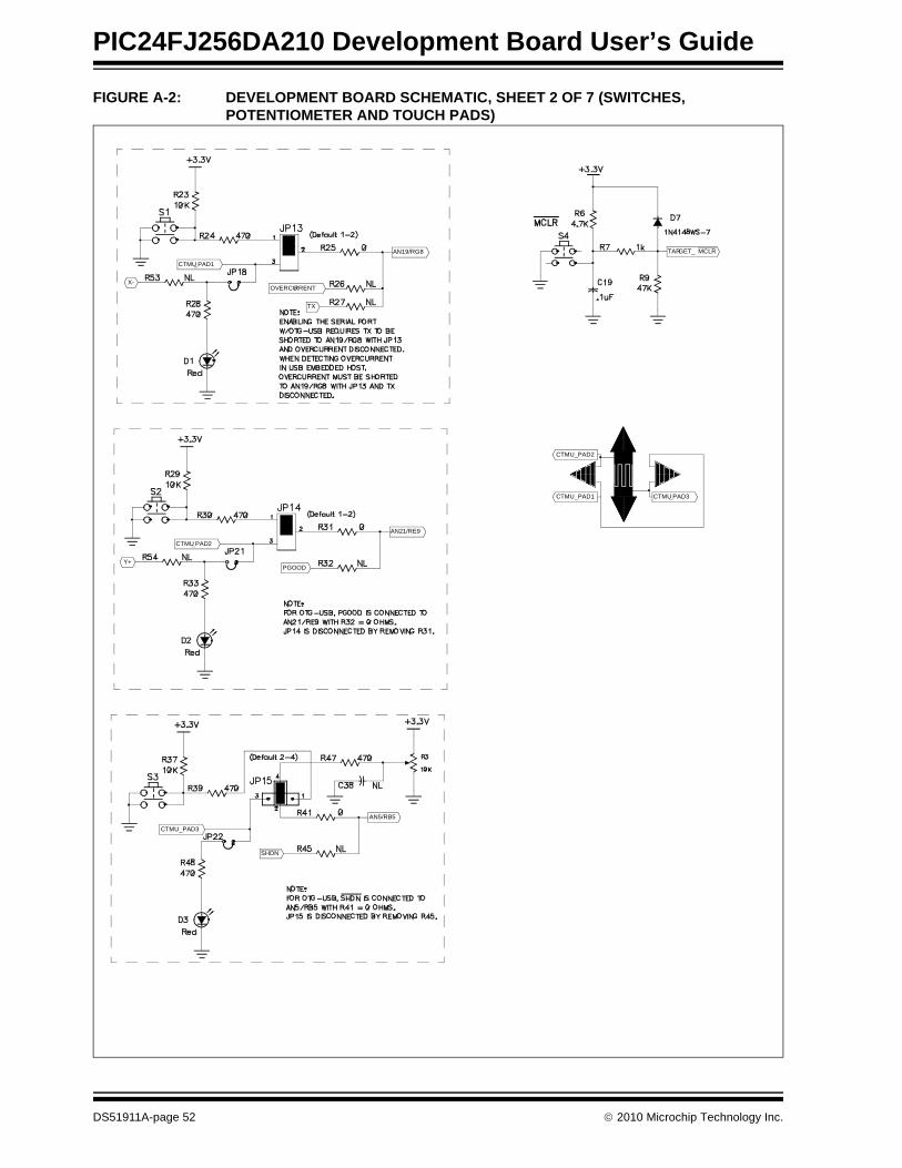
PIC24FJ256DA210 Development Board User’s Guide
FIGURE A-2: DEVELOPMENT BOARD SCHEMATIC, SHEET 2 OF 7 (SWITCHES, POTENTIOMETER AND TOUCH PADS)
CTMU_PAD2
CTMU_PAD1 CTMU_PAD3
TX
PGOODY+
CTMU_PAD2
X-OVERCURRENT
CTMU_PAD1
AN19/RG8
AN21/RE9
AN5/RB5
SHDN
CTMU_PAD3
TARGET_ MCLR
DS51911A-page 52 2010 Microchip Technology Inc.

Development Board Schematics
FIGURE A-3: DEVELOPMENT BOARD SCHEMATIC, SHEET 3 OF 7 (FLASH AND SRAM OPTIONS)
PMA17/RA7
PMRD/RD5
PMBE0
PMA14
PMA12
PMA8
PMA6
PMA2
PMA0
SPI_SCK
PMD15
PMD11
PMD9
PMD5
PMD3
PMA4
PMA6
PMA9
PMA13
PMA15
PMD1
PMD2
PMD12
PMD14
PMD15
PMA16
PMA16
PMWR/RD4
PMA4
PMA10
SPI_MOSI
PMD13
PMD1
PMD7
PMA2
PMA11
PMWR/RD4
PMD0
PMD3
PMD13
SPI_MISO
PMCS2
PMCS1
PMA15
PMA11
PMA9
PMA5
PMA3
PMA1
PMA3
PMA7
PMD14
PMD12
PMD8
PMA10
PMD6
PMA12
PMD2
PMD0
PMA0
PMRD/RD5
PMD8
PMD10
PMD11
PMD5
PMD6
PMA18
PMBE1
PMA13
PMA7
PMA1
PMA5
PMA14
PMA8
PMD10
PMD4
PMD9
PMD7
PMD4
PMA18_FOR_PT+
2010 Microchip Technology Inc. DS51911A-page 53

PIC24FJ256DA210 Development Board User’s Guide
FIGURE A-4: DEVELOPMENT BOARD SCHEMATIC, SHEET 4 OF 7 (USB AND UART OPTIONS, POWER SUPPLY)
USBID
D-
VBUS
D+
D-
D+
D-
PGOOD
SHDN
D+
VBUS
VBUS
OVERCURRENT
CTS
RTS
USART_RX
USART_TX
U1RX
U1TX
RX
TX
USART_TX
USART_RX
TARGET_3.3V
DS51911A-page 54 2010 Microchip Technology Inc.
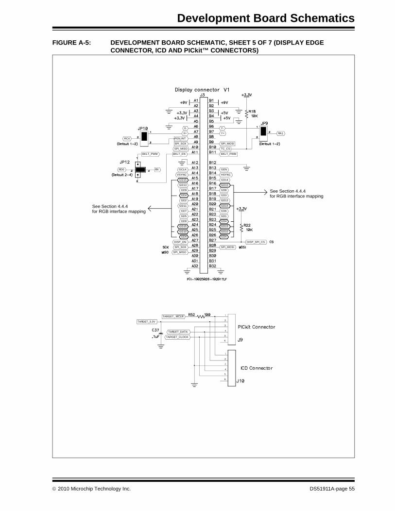
Development Board Schematics
FIGURE A-5: DEVELOPMENT BOARD SCHEMATIC, SHEET 5 OF 7 (DISPLAY EDGE CONNECTOR, ICD AND PICkit™ CONNECTORS)
SPI_MOSI
GD4
GD10
GD4
GD1
GD15
GD12
GD8
GD10
HSYNC
GEN
BKLT_PWM
SPI_MOSI
Y-
GD15
GD6
GD3
GD14
TC_CS
Y+
SPI_MISO
SPI_SCK
GD4
GD10
GD0
GD5
GD11
GD2
GD9
GD13
VSYNC
GCLKRD0 RX
BKLT_ENBKLT_PWM
SPI_SCK
PEN_INTRC4
X-
DISP_ON
GD15
GD7
GD4
GD15
SPI_MISO
X+
DISP_SPI_CS
RA1
TARGET_ MCLR
TARGET_3.3V
TARGET_DATA
TARGET_CLOCK
See Section 4.4.4for RGB interface mapping
See Section 4.4.4for RGB interface mapping
2010 Microchip Technology Inc. DS51911A-page 55

PIC24FJ256DA210 Development Board User’s Guide
FIGURE A-6: DEVELOPMENT BOARD SCHEMATIC, SHEET 6 OF 7 (PICtail™ PLUS CONNECTOR AND PICtail CONFIGURATION OPTIONS)
PMD4
PMD2
PMD12
RC13_TO_P101
PMD14
PMBE1_TO_P93
PMA1
PMA11
PMA18
PMA7
PMA3
PMA5
PMA2
PMD9
PMD8
PMBE1_TO_P17
SPI_MISO
SPI_SCK
PMD6
PMD0
PMWR/RD4
PMA13
PMBE1
PMA4
PMA18_TO_P19
SPI_MOSI
PMD5
PMD3
PMD13
PMD15
PMBE0
PMA0
PMA10
PMA6
PMA8
PMA9
U1TX
PMD7
PMD1
PMA15_TO_P103
PMA12
AN21/RE9_TO_P85
PMA16
PMCS2
AN5/RB5_TO_P13
AN19/RG8_TO_P1 U1RX
AN19/RG8_TO_P72
RC13_PMD10_TO_P30
PMBE1_PMD11_TO_P28
AN21/RE9_PMCS1_TO_P18
PMA18_TO_P12
PMA14_TO_P104
PMRD/RD5
PMA17/RA7
RC13_TO_P20
RC13_TO_P101
PMD10
PMD11
PMBE1_TO_P17
PMA14 PMA14_TO_P104
PMCS1
PMA15 PMA15_TO_P103
AN19/RG8_TO_P1
AN19/RG8 AN19/RG8_TO_P72
PMA18_TO_P19
AN5/RB5 AN5/RB5_TO_P13
RC13 RC13_TO_P20
PMBE1 PMBE1_TO_P93
AN21/RE9 AN21/RE9_TO_P85
PMA18_FOR_PT+ PMA18_TO_P12
PMBE1_PMD11_TO_P28
RC13_PMD10_TO_P30
AN21/RE9_PMCS1_TO_P18
See Appendix B for details
Samtec MEC1-160-02-S-D-A
DS51911A-page 56 2010 Microchip Technology Inc.
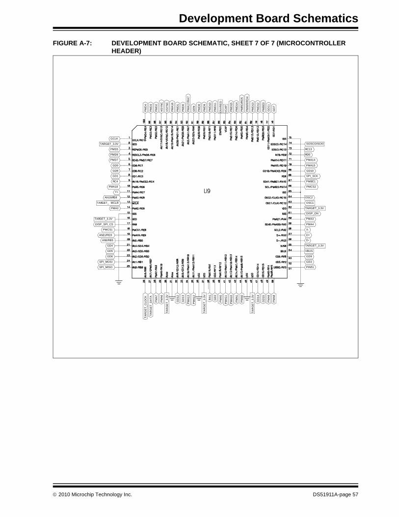
Development Board Schematics
FIGURE A-7: DEVELOPMENT BOARD SCHEMATIC, SHEET 7 OF 7 (MICROCONTROLLER HEADER)
PM
D3
PM
D2
VS
YN
C
PM
A1
6
PM
D0
PM
D8
PM
D9
PM
D11
PM
D15
PM
D14
PM
D13
PM
BE
0
GD
11
TA
RG
ET
_DA
TA
PM
A7
TA
RG
ET
_3
.3V
GD
13
PM
A1
3P
MA
17/
RA
7
TA
RG
ET
_3
.3V
GD
2
PM
A5
EN
VR
EG
PM
A1
0
PM
A1
PM
WR
/RD
4
TA
RG
ET
_3
.3V
GD
15
PM
A9
SPI_MISO
SPI_MOSI
GD5
GD4
AN21/RE9
PMCS1
TARGET_3.3V
TARGET_ MCLR
AN19/RG8
PMA18
RC4
GD8
GD0
PMD6
PMD5
GCLK
PIN51
GD3
VBUS
D+
X-
PMA3
OSC1
OSC2
PMBE1
GD10
PMA15
RD0
RC13
GD6
AN5/RB5
PMA2
DISP_SPI_CS
GD1
Y+
PMD7
TARGET_3.3VP
MD
4
PM
D1
GE
N
PM
D10
VC
AP
PM
D12
GD
7
GD9
D-
PMA4
PMA14
TA
RG
ET
_C
LOC
K
PM
A6
GD
12
HS
YN
C
PM
A1
2
RA
1
PM
A1
1
PM
A0
PM
RD
/RD
5
GD
14
PM
A8
TARGET_3.3V
DISP_ON
PMCS2
TARGET_3.3V
SPI_SCK
SOSCO/SCKI
2010 Microchip Technology Inc. DS51911A-page 57

PIC24FJ256DA210 Development Board User’s Guide
NOTES:
DS51911A-page 58 2010 Microchip Technology Inc.

PIC24FJ256DA210DEVELOPMENT BOARD
USER’S GUIDE
Appendix B. Modifications for PICtail Plus Daughter Boards
B.1 INTRODUCTION
This appendix provides a detailed description of the modifying the development board for use with different PICtail Plus daughter boards. Topics include:
• Overview of the PICtail Plus Interface
• Modifications for Specific Daughter Boards
B.2 OVERVIEW OF THE PICTAIL PLUS INTERFACE
To maximize their versatility, many of Microchip’s development and demonstration boards are equipped with the PICtail Plus interface. This allows boards with a standard-ized edge connector to directly access the I/O lines of each other’s microcontrollers and expand their functionality. In most cases, this is used to allow a more fully-featured board (such as the PIC24FJ256DA210 Development Board) to connect to a PICtail Plus daughter card and add new features to a pretape application (for example, adding 100 Mbps Ethernet using the Fast 100 Mbps Ethernet Daughter Board).
The basis for the design of the PICtail Plus interface is Microchip’s adherence to a stan-dard migration pathway throughout its microcontroller families: that is, for a given microcontroller package pin count, certain I/O ports are always located on specific pins of the PICtail Plus interface, and specific peripherals are almost always associated with specific I/O ports. This permits daughter boards to use a specific pin for SPI communi-cation, for example, because microcontrollers will always have an SPI peripheral asso-ciated with that I/O pin, and that PICtail Plus connector pin.
There are exceptions, however. Because of its complex graphics interface and enhanced PMP, the PIC24FJ256DA210 microcontroller does not map I/O ports and peripherals in the same way as other 100-pin devices are mapped. To maximize com-patibility, this requires a change of the PICtail Plus mapping for the PIC24FJ256DA210 Development Board. The complete mapping from microcontroller to interface are shown in Table B-1.
Since PICtail Plus-compatible daughter boards are designed to the standard interface, some additional remapping of the interface is needed to make the PIC24FJ256DA210 Development Board compatible. Provisions to do this are made by connecting a group of I/O lines the resistor bank described in Section 4.4.6 “PICtail™ Plus Card Modular Expansion Connector”. Populating or removing specific resistors in this bank allows the remapping of certain signals and restoring compatibility with specific daughter boards. As of this writing, the development board can be made compatible with all available PICtail Plus daughter boards.
A list of specific signals controlled by the resistor bank is provided in Table B-2; note that some signals are routed to multiple pins on the PICtail Plus interface by default to maximize compatibility. Table B-3 shows the same information to specifically highlight which signals can be remapped to a particular pin.
Section B.3 “Modifications for Specific Daughter Boards” describes the specific resistor changes required for each PICtail Plus daughter board.
2010 Microchip Technology Inc. DS51911A-page 59

PIC24FJ256DA210 Development Board User’s Guide
TABLE B-1: COMPLETE MICROCONTROLLER TO PICtail™ PLUS CONNECTOR PIN MAPPING
PICtail™ PlusPIC24FJ256DA210
I/O Pin (#)
PICtail PlusPIC24FJ256DA210
I/O Pin (#)PinStandard
SignalPin
Standard Signal
1 RB2 AN19/RG8/CTMU1 (12)(1) 68 RG14 PMA16 (95)
2 RF2 RP11/RD0 (72) 72 RA5 AN19/RG8/CTMU1 (12)(1)
3 RF6 RP2/RD8 (68) 74 RA7 PMA17/RA7 (92)
4 RF3 RP16/RF3 (51) 79 RB10 PMA13 (34)
5 RF7 AN1/RP1/RB1 (24) 80 RB11 PMA12 (35)
6 RG2 N/C 81 RB12 PMA11 (41)
7 RF8 AN0/RP0/RB0 (25) 82 RB13 PMA10 (42)
12 RB1 AN17/PMA18/RG6 (10)(1) 83 RB14 PMA1 (43)
13 RB3 AN5/RB5/CTMU3 (20) 84 RB15 PMA0 (44)
17 RE9 PMBE1/RA15 (67) 85 RC1 AN21/RE9/CTMU2 (19)(1)
18 RE8 AN21/RE9/CTMU2 (19)(1) 93 RD0 PMBE1/RA15 (67)(1)
19 RD14 AN17/PMA18/RG6 (10)(1) 96 RD3 PMBE0 (78)
20 RD15 RC13 (73) 97 RD4 PMWR (81)
27 RG0 N/C 98 RD5 PMRD (82)
28 RF0 PMBE1/RA15 (67)(1) 99 RD6 PMD14 (83)
29 RG1 PMD9 (89) 100 RD7 PMD15 (84)
30 RF1 RC13 (73) 101 RD8 RC13(73)
33 RG9 PMA2 (14) 103 RD10 PMA15 (70)
34 RF4 PMA9 (49) 104 RD11 PMA14 (71)
35 RG6 PMA5 (40) 105 RD12 PMD12 (35)
36 RF5 PMA8 (50) 106 RD13 PMD13 (34)
37 RG7 PMA4 (59) 109 RE0 PMD0 (93)
39 RG8 PMA3 (60) 110 RE1 PMD1 (94)
42 GND N/C 111 RE2 PMD2 (98)
45 RA9 PMA7 (28) 112 RE3 PMD3 (99)
46 RA10 PMA6 (29) 113 RE4 PMD4 (100)
49 RA15 PMBE1 (67) 114 RE5 PMD5 (3)
50 RA14 PMCS2 (66) 115 RE6 PMD6 (4)
51 RF12 PMA18 (10) 116 RE7 PMD7 (5)
Note 1: Each of these signals appears on two or more PICtail Plus pins.
DS51911A-page 60 2010 Microchip Technology Inc.

Modifications for PICtail Plus Daughter Boards
TABLE B-2: DEFAULT SIGNAL ROUTING TO PICtail™ PLUS CONNECTOR (BY SIGNAL)
TABLE B-3: DEFAULT AND OPTIONAL SIGNAL ROUTINGS TO PICtail™ PLUS CONNECTOR
Microcontroller Pin
PT+ Pin # Resistor PT+ Pin # Resistor PT+ Pin # Resistor
AN5/RB5 13 R40 (0) — — — —
AN19/RG8 1 R55 (0) 72 R36 (0) — —
AN21/RE9 85 R46 (0) 18 R57 (0) — —
PMA14 104 R59 (0) — — — —
PMA15 103 R56 (0) — — — —
PMA18 12 R34 (0) 19 R35 (0) — —
PMD10 30(1) R61 (N/C) — — — —
PMD11 28(1) R60 (N/C) — — — —
PMBE1 17 R42 (1k) 93 R43 (0) 28 R44 (0)
PMCS1 18(1) R58 (N/C) — — — —
RC13 20 R49 (0) 101 R50 (0) 30 R51 (0)
Legend: Parenthesis indicates resistance in ohms; N/C – no resistor present; PT+ – PICtail™ Plus
Note 1: Signal disconnected from this pin by default.
PICtail™ Plus Pin # Connected Signal(s) Optional Signal(s)
1 AN19/RG8(1) —
12 PMA18(1) —
13 AN5/RB5 —
17 PMBE1 —
18 AN21/RE9(1) PMCS1
19 PMA18(1) —
20 RC13(1) —
28 PMBE1(1) PMD11
30 RC13(1) PMD10
72 AN19/RG8(1) —
85 AN21/RE9(1) —
93 PMBE1(1) —
101 RC13(1) —
103 PMA13 —
104 PMA14 —
Note 1: Signal appears on multiple PICtail Plus pins by default.
2010 Microchip Technology Inc. DS51911A-page 61

PIC24FJ256DA210 Development Board User’s Guide
B.3 MODIFICATIONS FOR SPECIFIC DAUGHTER BOARDS
The configuration resistor changes that are required to make the development board function with available PICtail Plus daughter boards are listed below. This list is com-plete for compatible boards that were available at the time of publication. Note that some daughter boards are compatible as provided, and that no modifications are required.
Daughter boards released by Microchip subsequent to this publication may be compat-ible with the development board. The user may use the schematics in Appendix A and the daughter board to verify signal compatibility.
B.3.1 Fast 100 Mbps Ethernet Daughter Board (AC164132)
Three hardware changes are required:
• Enable PMP Data 10 (PMD10) by populating R61 and removing R51
• Enable PMP Data 11 (PMD11) by populating R60 and removing R44
• Enable PMP CS signal (PMCS1) by populating R58 and removing R57
B.3.2 PICtail Board for SD & MMC (AC164122)
Two hardware changes are required:
• Enable Write Protect (WD) by populating R51 (default) and removing R61
• Enable Card Detect (CD) by populating R60 (default) and removing R44
B.3.3 MRF49XA PICtail/PICtail Plus Daughter Board (AC164137-1 and AC164137-2)
One hardware change is required:
• Enable EEPROM Chip Select (EE_nCS) by populating R51 (default) and removing R61
B.3.4 Directly Compatible Daughter Boards
No hardware modifications to the PIC24FJ256DA210 Development Board are required when these daughter boards are used:
• Ethernet PICtail Plus Daughter Board (AC164123)
• Speech Playback PICtail Plus Daughter Board (AC164125)
• IrDA PICtail Plus Daughter Board (AC164124)
DS51911A-page 62 2010 Microchip Technology Inc.

PIC24FJ256DA210DEVELOPMENT BOARD
USER’S GUIDE
Index
BBuilding Code...................................................................... 22
CConfiguration
Analog Input (Potentiometer) ...................................... 37Board Configuration vs Availability of Features .......... 35EPMP Alternate Configuration .................................... 48External Memory
Flash Memory ..................................................... 45SRAM ................................................................. 43
Graphics Port .............................................................. 41Backlight Control................................................. 43Touch Screen Interface ...................................... 42
Jumper Locations.................................................. 34, 50LEDs ........................................................................... 37PICtail Plus Connector
Hardware Modifications .......................... 47, 59–62PICtail Plus Connector................................................ 46Push Button Switches ................................................. 36Touch Sensors............................................................ 37UART .......................................................................... 39
RX Signal and Backlight ..................................... 41TX Remapping.................................................... 40
USB....................................................................... 38–39Connectors.......................................................................... 49CTMU Touch Sensors ........................................................ 37Current Measurement ......................................................... 47Customer Notification Service............................................... 9Customer Support ................................................................. 9
DDebugging Code ................................................................. 27Demonstration Application (pre-programmed) .................... 17Demonstration Programs .................................................... 15Development Board Block Diagram.................................... 32Diagrams
Block Diagram............................................................. 32Configuring User-Defined Features ............................ 36Current Measurement ................................................. 48Development Board Layout ........................................ 12Flash Memory Configuration....................................... 45Jumper Locations........................................................ 34PICtail Plus Configuration Resistors ........................... 47SRAM Configuration ................................................... 44Touch Controller and Backlight Configuration ............ 42UART Configuration.................................................... 40USB Mode Configuration ............................................ 38
DocumentationConventions .................................................................. 6Layout ........................................................................... 5
EExternal SRAM ................................................................... 43
FFlash Memory ..................................................................... 45
IInternet Address ................................................................... 8
LLoading a Software Project................................................. 20
MMCLR ....................................................................... 33, 16, 8
OOscillator Options ............................................................... 33
PPCB Layout Features ......................................................... 32PICtail Plus Connector Pin Mapping................................... 60Potentiometer ..................................................................... 37Power Requirements .......................................................... 13Power Supply Options ........................................................ 33Programming the PIC24FJ256DA210 ................................ 23Programming/Debugging Interface..................................... 33Push Button Switches......................................................... 36
RReading, Recommended...................................................... 7Reset Switch....................................................................... 33Running Code..................................................................... 26
SSchematics ................................................................... 51–57Software for Application Development................................ 16
UUART.................................................................................. 39USB On-the-Go mode ........................................................ 39Using Breakpoints and Mouseovers ................................... 28Using Watch Windows........................................................ 29
WWWW Address ..................................................................... 8
2010 Microchip Technology Inc. DS51911A-page 63

DS51911A-page 64 2010 Microchip Technology Inc.
AMERICASCorporate Office2355 West Chandler Blvd.Chandler, AZ 85224-6199Tel: 480-792-7200 Fax: 480-792-7277Technical Support: http://support.microchip.comWeb Address: www.microchip.com
AtlantaDuluth, GA Tel: 678-957-9614 Fax: 678-957-1455
BostonWestborough, MA Tel: 774-760-0087 Fax: 774-760-0088
ChicagoItasca, IL Tel: 630-285-0071 Fax: 630-285-0075
ClevelandIndependence, OH Tel: 216-447-0464 Fax: 216-447-0643
DallasAddison, TX Tel: 972-818-7423 Fax: 972-818-2924
DetroitFarmington Hills, MI Tel: 248-538-2250Fax: 248-538-2260
KokomoKokomo, IN Tel: 765-864-8360Fax: 765-864-8387
Los AngelesMission Viejo, CA Tel: 949-462-9523 Fax: 949-462-9608
Santa ClaraSanta Clara, CA Tel: 408-961-6444Fax: 408-961-6445
TorontoMississauga, Ontario, CanadaTel: 905-673-0699 Fax: 905-673-6509
ASIA/PACIFICAsia Pacific OfficeSuites 3707-14, 37th FloorTower 6, The GatewayHarbour City, KowloonHong KongTel: 852-2401-1200Fax: 852-2401-3431
Australia - SydneyTel: 61-2-9868-6733Fax: 61-2-9868-6755
China - BeijingTel: 86-10-8528-2100 Fax: 86-10-8528-2104
China - ChengduTel: 86-28-8665-5511Fax: 86-28-8665-7889
China - ChongqingTel: 86-23-8980-9588Fax: 86-23-8980-9500
China - Hong Kong SARTel: 852-2401-1200 Fax: 852-2401-3431
China - NanjingTel: 86-25-8473-2460Fax: 86-25-8473-2470
China - QingdaoTel: 86-532-8502-7355Fax: 86-532-8502-7205
China - ShanghaiTel: 86-21-5407-5533 Fax: 86-21-5407-5066
China - ShenyangTel: 86-24-2334-2829Fax: 86-24-2334-2393
China - ShenzhenTel: 86-755-8203-2660 Fax: 86-755-8203-1760
China - WuhanTel: 86-27-5980-5300Fax: 86-27-5980-5118
China - XianTel: 86-29-8833-7252Fax: 86-29-8833-7256
China - XiamenTel: 86-592-2388138 Fax: 86-592-2388130
China - ZhuhaiTel: 86-756-3210040 Fax: 86-756-3210049
ASIA/PACIFICIndia - BangaloreTel: 91-80-3090-4444 Fax: 91-80-3090-4123
India - New DelhiTel: 91-11-4160-8631Fax: 91-11-4160-8632
India - PuneTel: 91-20-2566-1512Fax: 91-20-2566-1513
Japan - YokohamaTel: 81-45-471- 6166 Fax: 81-45-471-6122
Korea - DaeguTel: 82-53-744-4301Fax: 82-53-744-4302
Korea - SeoulTel: 82-2-554-7200Fax: 82-2-558-5932 or 82-2-558-5934
Malaysia - Kuala LumpurTel: 60-3-6201-9857Fax: 60-3-6201-9859
Malaysia - PenangTel: 60-4-227-8870Fax: 60-4-227-4068
Philippines - ManilaTel: 63-2-634-9065Fax: 63-2-634-9069
SingaporeTel: 65-6334-8870Fax: 65-6334-8850
Taiwan - Hsin ChuTel: 886-3-6578-300Fax: 886-3-6578-370
Taiwan - KaohsiungTel: 886-7-536-4818Fax: 886-7-536-4803
Taiwan - TaipeiTel: 886-2-2500-6610 Fax: 886-2-2508-0102
Thailand - BangkokTel: 66-2-694-1351Fax: 66-2-694-1350
EUROPEAustria - WelsTel: 43-7242-2244-39Fax: 43-7242-2244-393Denmark - CopenhagenTel: 45-4450-2828 Fax: 45-4485-2829
France - ParisTel: 33-1-69-53-63-20 Fax: 33-1-69-30-90-79
Germany - MunichTel: 49-89-627-144-0 Fax: 49-89-627-144-44
Italy - Milan Tel: 39-0331-742611 Fax: 39-0331-466781
Netherlands - DrunenTel: 31-416-690399 Fax: 31-416-690340
Spain - MadridTel: 34-91-708-08-90Fax: 34-91-708-08-91
UK - WokinghamTel: 44-118-921-5869Fax: 44-118-921-5820
WORLDWIDE SALES AND SERVICE
01/05/10