Embed Size (px)
Citation preview

PIC16(L)F188XX PIC16(L)F188XX Memory Programming Specification
1.0 OVERVIEW
This Programming Specification describes an SPI-based programming method for the PIC16(L)F188XX family ofmicrocontrollers. Section 3.0 “Programming Algorithms” describes the programming commands, programmingalgorithms and electrical specifications which are used in that particular programming method. Appendix B containsindividual part numbers, device identification and checksum values, pinout and packaging information and ConfigurationWords.
1.1 Programming Data Flow
Nonvolatile Memory (NVM) programming data can be supplied by either the high-voltage In-Circuit SerialProgramming™ (ICSP™) interface or the low-voltage In-Circuit Serial Programming (ICSP) interface. Data can beprogrammed into the Program Flash Memory (PFM), Data Flash Memory (EEPROM), dedicated “user ID” locations andthe Configuration Words.
1.2 Write and/or Erase Selection
Erasing or writing is selected according to the command used to begin operation (see Table 3-1). The terminologiesused in this document related to erasing/writing to the program memory are defined in Table 1-1 and are detailed below.
1.2.1 ERASING MEMORY
Memory is erased by row or in bulk, where ‘bulk’ includes many subsets of the total memory space. The duration of theerase is always determined internally. All Bulk ICSP Erase commands have minimum VDD requirements, which arehigher than the row erase and write requirements.
1.2.2 WRITING MEMORY
Memory is written one row at a time. Multiple Load Data for NVM commands are used to fill the row data latches. Theduration of the write is determined either internally or externally.
1.2.3 MULTI-WORD PROGRAMMING INTERFACE
Program Flash Memory (PFM) panels include a 32-word (one row) programming interface. The row to be programmedmust first be erased either with a Bulk Erase or a Row Erase.
Note 1: This is a new SPI-compatible programming method with 8-bit commands.
2: The low-voltage entry code is now 32 clocks and MSb, not 33 clocks as in the PIC16(L)F183XX devicefamily.
TABLE 1-1: PROGRAMMING TERMS
Term Definition
Programmed Cell A memory cell with a logic ‘0’
Erased Cell A memory cell with a logic ‘1’
Erase Change memory cell from a ‘0’ to a ‘1’
Write Change memory cell from a ‘1’ to a ‘0’
Program Generic Erase and/ or Write
2014 Microchip Technology Inc. DS40001753B-page 1

PIC16(L)F188XX
1.3 Hardware Requirements
1.3.1 HIGH-VOLTAGE ICSP PROGRAMMING
In High-Voltage ICSP mode, the device requires two programmable power supplies: one for VDD and one for the MCLR/VPP pin.
1.3.2 LOW-VOLTAGE ICSP PROGRAMMING
In Low-Voltage ICSP mode, the device can be programmed using a single VDD source in the operating range. TheMCLR/VPP pin does not have to be brought to a different voltage, but can instead be left at the normal operating voltage.
1.3.2.1 Single-Supply ICSP Programming
The LVP bit enables single-supply (low-voltage) ICSP programming. The LVP bit defaults to a ‘1’ (enabled) from thefactory. The LVP bit may only be programmed to ‘0’ by entering the High-Voltage ICSP mode, where the MCLR/VPP pinis raised to VIHH. Once the LVP bit is programmed to a ‘0’, only the High-Voltage ICSP mode is available and only theHigh-Voltage ICSP mode can be used to program the device.
1.4 Pin Utilization
Five pins are needed for ICSP programming. The pins are listed in Table 1-2. For pin locations and packaginginformation please refer to Table B-2.
Note 1: The High-Voltage ICSP mode is always available, regardless of the state of the LVP bit, by applying VIHH
to the MCLR/VPP pin.
2: While in Low-Voltage ICSP mode, MCLR is always enabled, regardless of the MCLRE bit, and the portpin can no longer be used as a general purpose input.
TABLE 1-2: PIN DESCRIPTIONS DURING PROGRAMMING
Pin NameDuring Programming
Function Pin Type Pin Description
ICSPCLK ICSPCLK I Clock Input – Schmitt Trigger Input
ICSPDAT ICSPDAT I/O Data Input/Output – Schmitt Trigger Input
MCLR/VPP Program/Verify mode I(1) Program Mode Select
VDD VDD P Power Supply
VSS VSS P Ground
Legend: I = Input, O = Output, P = PowerNote 1: The programming high voltage is internally generated. To activate the Program/Verify mode, high voltage
needs to be applied to MCLR input. Since the MCLR is used for a level source, MCLR does not draw any significant current.
DS40001753B-page 2 2014 Microchip Technology Inc.
PIC16(L)F188XX
2.0 MEMORY MAPFIGURE 2-1: PROGRAM MEMORY MAPPING
PIC16(L)F18854PIC16(L)F18855PIC16(L)F18875
PIC16(L)F18856PIC16(L)F18876
PIC16(L)F18857PIC16(L)F18877
PC<15:0>(5) PC<15:0>(5) PC<15:0>(5) PC<15:0>(5)
Note 1 Stack (16 levels) Stack (16 levels) Stack (16 levels) Stack (16 levels)
0000h
Program Flash Memory
Program Flash Memory
Program Flash Memory
Program Flash Memory
0FFFh
1000h•
1FFFh
Unimplemented(4)
2000h••
3FFFh
Unimplemented(4)4000h••••
7FFFh
Unimplemented(4)
8000h• • •
8003hUser IDs(2)
8004h Reserved
8005h Revision ID(2,3)
8006h Device ID(2,3)
8007h• • •
800BhConfiguration Word 1,2,3,4,5(2)
800Ch••••••••••••
EFFFh
Reserved
F000h• • •
F0FFhUser Data Memory (EEPROM)
• • •FFFFh
Reserved
Note 1: The stack is a separate SRAM panel, apart from all user memory panels.2: Not code-protected.3: Device/Revision IDs are hard-coded in silicon.4: The addresses do not roll over. The region is read as ‘0’.5: For the purposes of instruction fetching during program execution, only 15 bits (PC<14:0>) are used. However, for the
purposes of non-volatile memory reading and writing through ICSP programming operations, the PC uses all 16 bits (PC<15:0>), and the "Load PC Address" command requires a full 16-bit data payload.
2014 Microchip Technology Inc. DS40001753B-page 3
PIC16(L)F188XX
2.1 User ID Location
A user may store identification information (user ID) in four designated locations. The user ID locations are mapped to8000h-8003h. Each location is 14 bits in length. Code protection has no effect on these memory locations. Each locationmay be read with code protection enabled or disabled.
2.2 Device/Revision ID
The 14-bit device ID word is located at 8006h and the 14-bit revision ID is located at 8005h. These locations areread-only and cannot be erased or modified.
REGISTER 2-1: DEVICEID: DEVICE ID REGISTER
R R R R R R R R R R R R R R
1 1 DEV11 DEV10 DEV9 DEV8 DEV7 DEV6 DEV5 DEV4 DEV3 DEV2 DEV1 DEV0
bit 13 bit 0
Legend:
R = Readable bit
‘0’ = Bit is cleared ‘1’ = Bit is set x = Bit is unknown
bit 13-12 Fixed Value: Read-only bitsThese bits are fixed with value ‘11’ for all devices included in this programming specification.
bit 11-0 DEV<11:0>: Device ID bits
Note: Refer to Table B-1 for a list of device ID register values for the devices covered by this programmingspecification document.
REGISTER 2-2: REVISIONID: REVISION ID REGISTER
R R R R R R R R R R R R R R
1 0 MJRREV<5:0> MNRREV<5:0>
bit 13 bit 0
Legend:
R = Readable bit
‘0’ = Bit is cleared ‘1’ = Bit is set x = Bit is unknown
bit 13-12 Fixed Value: Read-only bitsThese bits are fixed with value ‘10’ for all devices included in this programming specification.
bit 11-6 MJRREV<5:0>: Major Revision ID bits
These bits are used to identify a major revision. A major revision is indicated by an all layer revision (B0,C0, etc.)
bit 5-0 MNRREV<5:0>: Minor Revision ID bitsThese bits are used to identify a minor revision.
DS40001753B-page 4 2014 Microchip Technology Inc.

PIC16(L)F188XX
2.3 Configuration Words
The devices have several Configuration Words starting at address 8007h. The individual bits within these ConfigurationWords are critical to the correct operation of the system. Configuration bits enable or disable specific features, placingthese controls outside the normal software process, and they establish configured values prior to the execution of anysoftware.
In terms of programming, these important Configuration bits should be considered:
1. LVP: Low-Voltage Programming Enable bit
• 1 = ON - Low-Voltage Programming is enabled. MCLR/VPP pin function is MCLR. MCLRE Configuration bit is ignored.
• 0 = OFF - HV on MCLR/VPP must be used for programming.
It is important to note that the LVP bit cannot be written (to 0) while operating from the LVP programming interface. Thepurpose of this rule is to prevent the user from dropping out of LVP mode while programming from LVP mode, oraccidentally eliminating LVP mode from the configuration state. For more information, see Section 3.1.2 “Low-VoltageProgramming (LVP) Mode”.
2. CPD: Data NVM (EEPROM) Memory Code Protection bit
• 1 = OFF - Data NVM code protection disabled• 0 = ON - Data NVM code protection enabled
3: CP: User NVM Program Memory Code Protection bit
• 1 = OFF - User NVM code protection disabled• 0 = ON - User NVM code protection enabled
For more information on code protection, see Section 3.3 “Code Protection”.
2014 Microchip Technology Inc. DS40001753B-page 5
PIC16(L)F188XX
3.0 PROGRAMMING ALGORITHMS
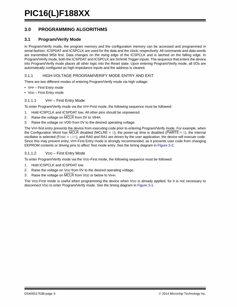
3.1 Program/Verify Mode
In Program/Verify mode, the program memory and the configuration memory can be accessed and programmed inserial fashion. ICSPDAT and ICSPCLK are used for the data and the clock, respectively. All commands and data wordsare transmitted MSb first. Data changes on the rising edge of the ICSPCLK and is latched on the falling edge. InProgram/Verify mode, both the ICSPDAT and ICSPCLK are Schmitt Trigger inputs. The sequence that enters the deviceinto Program/Verify mode places all other logic into the Reset state. Upon entering Program/Verify mode, all I/Os areautomatically configured as high-impedance inputs and the address is cleared.
3.1.1 HIGH-VOLTAGE PROGRAM/VERIFY MODE ENTRY AND EXIT
There are two different modes of entering Program/Verify mode via high voltage:
• VPP – First Entry mode
• VDD – First Entry mode
3.1.1.1 VPP – First Entry Mode
To enter Program/Verify mode via the VPP-First mode, the following sequence must be followed:
1. Hold ICSPCLK and ICSPDAT low. All other pins should be unpowered.
2. Raise the voltage on MCLR from 0V to VIHH.
3. Raise the voltage on VDD from 0V to the desired operating voltage.
The VPP-first entry prevents the device from executing code prior to entering Program/Verify mode. For example, whenthe Configuration Word has MCLR disabled (MCLRE = 0), the power-up time is disabled (PWRTE = 0), the internaloscillator is selected (FOSC = 100), and RA0 and RA1 are driven by the user application, the device will execute code.Since this may prevent entry, VPP-First Entry mode is strongly recommended, as it prevents user code from changingEEPROM contents or driving pins to affect Test mode entry. See the timing diagram in Figure 3-2.
3.1.1.2 VDD – First Entry Mode
To enter Program/Verify mode via the VDD-First mode, the following sequence must be followed:
1. Hold ICSPCLK and ICSPDAT low.
2. Raise the voltage on VDD from 0V to the desired operating voltage.
3. Raise the voltage on MCLR from VDD or below to VIHH.
The VDD-First mode is useful when programming the device when VDD is already applied, for it is not necessary todisconnect VDD to enter Program/Verify mode. See the timing diagram in Figure 3-1.
DS40001753B-page 6 2014 Microchip Technology Inc.

PIC16(L)F188XX
3.1.1.3 Program/Verify Mode Exit
To exit Program/Verify mode, lower MCLR from VIHH or lower (VIL). VDD-First Entry mode should use VDD-Last Exitmode (see Figure 3-1). VPP-First Entry mode should use VPP-Last Exit mode (see Figure 3-2).
FIGURE 3-1: PROGRAMMING ENTRY AND EXIT MODES – VPP FIRST AND LAST
FIGURE 3-2: PROGRAMMING ENTRY AND EXIT MODES – VDD FIRST AND LAST
PROGRAMMING MODE ENTRY – EXIT
VPP LAST
TEXIT
PROGRAMMING MODE ENTRY – ENTRY
VPP FIRST
TENTS TENTH
VDD
VIHH
VPP
ICSPDAT
ICSPCLK
VIL
PROGRAMMING MODE ENTRY – ENTRY
VDD FIRST
PROGRAMMING MODE ENTRY – EXIT
VDD LAST
TENTS TENTH
VDD
VIHH
VPP
ICSPDAT
ICSPCLK
VIL
TEXIT
2014 Microchip Technology Inc. DS40001753B-page 7

PIC16(L)F188XX
3.1.2 LOW-VOLTAGE PROGRAMMING (LVP) MODE
The Low-Voltage Programming mode allows the devices to be programmed using VDD only, without high voltage. Whenthe LVP bit of the Configuration Word 3 register is set to ‘1’, the low-voltage ICSP programming entry is enabled. Todisable the Low-Voltage ICSP mode, the LVP bit must be programmed to ‘0’. This can only be done while in theHigh-Voltage Entry mode.
Entry into the Low-Voltage ICSP Program/Verify mode requires the following steps:
1. MCLR is brought to VIL
2. A 32-bit key sequence is presented on ICSPDAT. The LSb of pattern is a “don’t care x”. The program/verifymode entry pattern detect hardware verifies only the first 31 bits of the sequence and the last clock is requiredbefore the pattern detect goes active.
The key sequence is a specific 32-bit pattern, '32’h4d434850' (more easily remembered as MCHP in ASCII). Thedevice will enter Program/Verify mode only if the sequence is valid. The Most Significant bit of the Most Significant nibblemust be shifted in first. Once the key sequence is complete, MCLR must be held at VIL for as long as Program/Verifymode is to be maintained. For low-voltage programming timing, see Figure 3-3 and Figure 3-4.
FIGURE 3-3: LVP ENTRY (POWERING-UP)
FIGURE 3-4: LVP ENTRY (POWERED)
Exiting Program/Verify mode is done by raising MCLR from below VIL to VIH level (or higher, up to VDD).
Note: To enter LVP mode, the MSb of the Most Significant nibble must be shifted in first. This differs from enteringthe key sequence on some other device families.
TCKLTCKH
32 Clocks
31 30 29 ... 1
TDHTDS
TENTH
MSb of Pattern LSb of Pattern
VDD
MCLR
ICSPDAT
TENTS
ICSPCLK
TCKH TCKL
32 Clocks
31 30 29 ... 1
TDHTDS
TENTH
MSb of Pattern LSb of Pattern
VDD
MCLR
ICSPCLK
ICSPDAT
DS40001753B-page 8 2014 Microchip Technology Inc.

PIC16(L)F188XX
3.1.3 PROGRAM/VERIFY COMMANDS
Once a device has entered ICSP Program/Verify mode (using either high voltage or LVP entry), the programming host devicemay issue seven commands to the microcontroller, each eight bits in length. The commands are summarized in Table 3-1.The commands are used to erase and program the device. The commands load and use the Program Counter (PC).
Some of the eight-bit commands also have a data payload associated with it (such as Load Data for NVM and ReadData from NVM).
If the programming host device issues an 8-bit command byte that has a data payload associated with it, the host deviceis responsible for sending an additional 24 clock pulses (for example, three 8-bit bytes), in order to send or receive thepayload data associated with the command.
The actual useful payload bits associated with a command are command-specific and will be less than 24 bits. However,the payload field is always padded with additional Start, Stop and Pad bits, to bring the total payload field size to 24 bits,so as to be compatible with many 8-bit SPI-based systems.
Within a 24-bit payload field, the first bit transmitted is always a Start bit, followed by a variable number of Pad bits,followed by the useful data payload bits and ending with one Stop bit. The useful data payload bits are alwaystransmitted Most Significant bit (MSb) first.
When the programming device issues a command that involves a host to microcontroller payload (for example, LoadPC Address), the Start, Stop and Pad bits should all be driven by the programmer to ‘0’. When the programming hostdevice issues a command that involves microcontroller to host payload data (for example, Read Data from NVM), theStart, Stop and Pad bits should be treated as “don't care” bits and the values should be ignored by the host.
When the programming host device issues an 8-bit command byte to the microcontroller, the host should wait aminimum amount of delay (which is command-specific) prior to sending any additional clock pulses (associated witheither a 24-bit data payload field or the next command byte).
TABLE 3-1: ICSP™ COMMAND SET SUMMARY
Command Name
Command ValuePayload
ExpectedDelay after Command
Data/NoteBinary (MSb … LSb)
Hex
Load PC Address 1000 0000 80 Yes TDLY PC = payload value
Bulk Erase Program Memory
0001 1000 18 No TERAB Depending on the current value of the PC, one or more memory regions.
Row Erase Program Memory
1111 0000 F0 No TERAR The row addressed by the MSbs of the PC is erased; LSbs are ignored.
Load Data for NVM 0000 00J0 00/02 Yes TDLY J = 1; PC = PC + 1 after writing;J = 0; PC is unchanged
Read Data from NVM 1111 11J0 FE/FC Yes TDLY J = 1; PC = PC + 1 after reading;J = 0; PC is unchanged
Increment Address 1111 1000 F8 No TDLY PC = PC + 1Begin Internally Timed Programming
1110 0000 E0 No TPINT Commits latched data to NVM(self timed)
Begin Externally Timed Programming
1100 0000 C0 No TPEXT Commits latched data to NVM(externally timed). After TPEXT, “End Externally Timed Programming” command must be issued.
End Externally TimedProgramming
1000 0010 82 No TDIS Should be issued within required time delay (TPEXT) after “Begin Externally Timed Programming” command.
2014 Microchip Technology Inc. DS40001753B-page 9

PIC16(L)F188XX
FIGURE 3-5: CLOCK AND DATA TIMING
3.1.3.1 Load Data for NVM
The Load Data for NVM command is used to load one programming data latch (for example, one 14-bit instruction wordfor program memory/configuration memory/user ID memory, or one 8-bit byte for an EEPROM data memory address).The word programs into program memory after the Begin Internally Timed Programming or Begin Externally TimedProgramming command is issued. The Load Data for NVM command can be used to load data for Program FlashMemory (PFM) (see Figure 3-6) or the Data Flash Memory (DFM) (see Figure 3-7). Depending on the value of bit 1 of thecommand, the PC may or may not be incremented (see Table 3-1).
FIGURE 3-6: LOAD DATA FOR NVM (PFM)
Note: All clock pulses for both the 8-bit commands and the 24-bit payload fields are generated by the hostprogramming device. The microcontroller does not drive the ICSPCLK line. The ICSPDAT signal is abidirectional data line. For all commands and payload fields, except the Read Data from NVM payload, thehost programming device continuously drives the ICSPDAT line. Both the host programmer device and themicrocontroller should latch received ICSPDAT values on the falling edge of the ICSPCLK line. When themicrocontroller is receiving ICSPDAT line values from the host programmer, the ICSPDAT values must bevalid a minimum of TDS before the falling edges of ICSPCLK and should remain valid for a minimum of TDH
after the falling edge of ICSPDAT. See Figure 3-5.
as
ICSPCLK
TCKH TCKL
TDHTDS
ICSPDAT
output
TCO
ICSPDAT
ICSPDAT
ICSPDAT
TLZD
THZD
input
as
from input
from output to input
to output
ICSPCLK
ICSPDAT
7 6 5 4 3 2 23 22 1 0
00 0 MSb0 0 0
TDLY
1 0 1415
0 J 0 00 LSb
Stop BitStart Bit
8-Bit Command 24-Bit Payload Field
0
TDLY
DS40001753B-page 10 2014 Microchip Technology Inc.

PIC16(L)F188XX
FIGURE 3-7: LOAD DATA FOR NVM (DFM)
ICSPCLK
ICSPDAT
7 6 5 4 3 2 23 22 1 0
00 0 MSb0 0 0
TDLY
1 0 89
0 J 0 00 LSb
Stop BitStart Bit
8-Bit Command 24-Bit Payload Field
0
TDLY
2014 Microchip Technology Inc. DS40001753B-page 11

PIC16(L)F188XX
3.1.3.2 Read Data from NVM
The Read Data from NVM command will transmit data bits out of the current PC address. The ICSPDAT pin will go intoOutput mode on the first falling edge of ICSPCLK, and it will revert to Input mode (high-impedance) after the 24th fallingedge of the clock. The Start and Stop bits are only one half of a bit time wide, and should therefore be ignored by thehost programmer device (since the latched value may be indeterminate). Additionally, the host programmer deviceshould only consider the MSb to LSb payload bits as valid, and should ignore the values of the pad bits. If the programmemory is code-protected (CP), the data will be read as zeros (see Figure 3-8 and Figure 3-9). Depending on the valueof bit ‘1’ of the command, the PC may or may not be incremented (see Table 3-1). The Read Data for NVM commandcan be used to read data for Program Flash Memory (PFM) (see Figure 3-8) or the Data Flash Memory (DFM) (seeFigure 3-9).
FIGURE 3-8: READ DATA FROM NVM (PFM OR CONFIGURATION WORDS)
FIGURE 3-9: READ DATA FROM NVM (DFM – EEPROM)
ICSPCLK
ICSPDAT
7 6 5 4 3 2 23 22 1 0
11 0
MSb
1 1 1
TDLY
1 0 1415
1 J
LSb
StopStart
(from Programmer)
ICSPDAT
(from device)Data
High-Z
0 0
Input
High-Z
InputOutput
TDLY
x x
ICSPCLK
ICSPDAT
23 22 1 0
11 0
MSb
1 1 1
TDLY
89
1 J
LSb
StopStart
(from Programmer)
ICSPDAT(from device)
Data
High-Z
0 0High-Z
7 6 5 4 3 2 1 0
Input InputOutput
TDLY
x x
DS40001753B-page 12 2014 Microchip Technology Inc.

PIC16(L)F188XX
3.1.3.3 Increment Address
The address is incremented by one when this command is received. It is not possible to decrement the address. Toreset this counter, the user must use the Load PC Address command. See Figure 3-10.
FIGURE 3-10: INCREMENT ADDRESS
3.1.3.4 Load PC Address
The PC value is set using the supplied data. The address implies the memory panel (PFM or DFM) to be accessed (seeFigure 3-11).
FIGURE 3-11: LOAD PC ADDRESS
ICSPCLK
ICSPDAT
7 6 5 4 3 2 7 6
01 01 1 1
1 0
1 0
TDLY
5
Next Command
X X X
Address + 1Address
ICSPCLK
ICSPDAT00 0 MSb1 0 0
TDLY
0 0 0 00 LSb
StopStart
Address 0
23 22 1 016177 6 5 4 3 2 1 0
TDLY
2014 Microchip Technology Inc. DS40001753B-page 13

PIC16(L)F188XX
3.1.3.5 Begin Internally Timed Programming
The write programming latches must already have been loaded using the Write Data for NVM command, prior to issuingthe Begin Programming command. Programming of the addressed memory will begin after this command is received.An internal timing mechanism executes the write. The user must allow for the Erase/Write cycle time, TPINT, in order forthe programming to complete, prior to issuing the next command byte (see Figure 3-12).
After the programming cycle is complete all the data latches are reset to ‘1’.
FIGURE 3-12: BEGIN INTERNALLY TIMED PROGRAMMING
3.1.3.6 Begin Externally Timed Programming
Data to be programmed must be previously loaded by Load Data for NVM command before every Begin Programmingcommand. To complete the programming, the End Externally Timed Programming command must be sent in the spec-ified time window defined by TPEXT (see Figure 3-13).
Externally timed writes are not supported for Configuration bits. Any externally timed write to the Configuration Word willhave no effect on the targeted word.
FIGURE 3-13: BEGIN EXTERNALLY TIMED PROGRAMMING
3.1.3.7 End Externally Timed Programming
This command is required to terminate the programming sequence after a Begin Externally Timed Programming com-mand is given. If no programming command is in progress or if the programming cycle is internally timed, this commandwill execute as No-operation (NOP) (Figure 3-14).
FIGURE 3-14: END PROGRAM TIMING
ICSPCLK
ICSPDAT
7 6 5 4 3 2 7 6
00 01 1 0
1 0
1 0
5
Next Command
X X X
TPINT
ICSPCLK
ICSPDAT
7 6 5 4 3 2 7 6
00 01 0 0
1 0
1 0
5
End Externally Timed Programming
1 0 0
TPEXT
Command
ICSPCLK
ICSPDAT
7 6 5 4 3 2 7 6
00 01 0 0
1 0
0 1
5
X X X
TDIS
Next Command
DS40001753B-page 14 2014 Microchip Technology Inc.
PIC16(L)F188XX
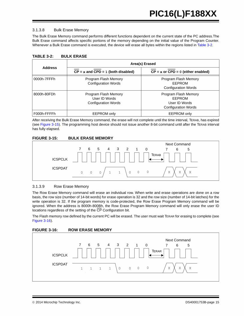
3.1.3.8 Bulk Erase Memory
The Bulk Erase Memory command performs different functions dependent on the current state of the PC address.TheBulk Erase command affects specific portions of the memory depending on the initial value of the Program Counter.Whenever a Bulk Erase command is executed, the device will erase all bytes within the regions listed in Table 3-2.
After receiving the Bulk Erase Memory command, the erase will not complete until the time interval, TERAB, has expired(see Figure 3-15). The programming host device should not issue another 8-bit command until after the TERAB intervalhas fully elapsed.
FIGURE 3-15: BULK ERASE MEMORY
3.1.3.9 Row Erase Memory
The Row Erase Memory command will erase an individual row. When write and erase operations are done on a rowbasis, the row size (number of 14-bit words) for erase operation is 32 and the row size (number of 14-bit latches) for thewrite operation is 32. If the program memory is code-protected, the Row Erase Program Memory command will beignored. When the address is 8000h-800Bh, the Row Erase Program Memory command will only erase the user IDlocations regardless of the setting of the CP Configuration bit.
The Flash memory row defined by the current PC will be erased. The user must wait TERAR for erasing to complete (seeFigure 3-16).
FIGURE 3-16: ROW ERASE MEMORY
TABLE 3-2: BULK ERASE
AddressArea(s) Erased
CP = x and CPD = 1 (both disabled) CP = x or CPD = 0 (either enabled)
0000h-7FFFh Program Flash MemoryConfiguration Words
Program Flash MemoryEEPROM
Configuration Words
8000h-80FDh Program Flash MemoryUser ID Words
Configuration Words
Program Flash MemoryEEPROM
User ID WordsConfiguration Words
F000h-FFFFh EEPROM only EEPROM only
ICSPCLK
ICSPDAT
7 6 5 4 3 2 7 6
01 00 0 1
1 0
0 0
5
Next Command
X X X
TERAB
ICSPCLK
ICSPDAT
7 6 5 4 3 2 7 6
00 01 1 1
1 0
1 0
5
Next Command
X X X
TERAR
2014 Microchip Technology Inc. DS40001753B-page 15

PIC16(L)F188XX
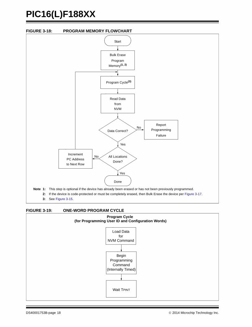
3.2 Programming Algorithms
The devices use internal latches to temporarily store the 14-bit words used for programming. The data latches allow theuser to write the program words with a single Begin Internally Timed Programming or Begin Externally TimedProgramming command. The Load Data for NVM command is used to load a single data latch. The data latch will holdthe data until the Begin Internally Timed Programming or Begin Externally Timed Programming command is given.
The data latches are aligned with the LSbs of the address. The address at the time the Begin Internally TimedProgramming or Begin Externally Timed Programming command is given will determine which memory row is written.Writes cannot cross a physical row boundary. For example, attempting to write from address 0002h-0021h in a 32-latchdevice will result in data being written to 0020h-003Fh.
If more than the maximum number of latches are written without a Begin Internally Timed Programming or BeginExternally Timed Programming command, the data in the data latches will be overwritten. Figure 3-17 through Figure 3-22 show the recommended flowcharts for programming.
Note: The program Flash memory and EEPROM memory regions are programmed one row (32 words) at a time(Figure 3-20), while the user ID and Configuration words are programmed one word at a time (Figure 3-19).
The value of the PC at the time of issuing the Begin Internally Timed Programming or Begin ExternallyTimed Programming command determines what row (of program Flash memory or EEPROM) or what word(of user ID or Configuration word) will get programmed.
DS40001753B-page 16 2014 Microchip Technology Inc.

PIC16(L)F188XX
FIGURE 3-17: DEVICE PROGRAM/VERIFY FLOWCHART
Done
Start
Bulk Erase
Device
Write User IDs
Enter
Programming Mode
Write Program Memory(1)
Verify User IDs
Write Configuration Words(2)
Verify Configuration Words
Exit Programming
Mode
Note 1: See Figure 3-11.
2: See Figure 3-16.
Write EEPROM
Verify EEPROM Memory
Verify Program Memory
2014 Microchip Technology Inc. DS40001753B-page 17
PIC16(L)F188XX
FIGURE 3-18: PROGRAM MEMORY FLOWCHART
FIGURE 3-19: ONE-WORD PROGRAM CYCLE
Start
Read Data
NVM
Data Correct?
Report
Programming
Failure
All Locations
Done?
No
NoIncrement
PC Address
to Next Row
from
Bulk Erase
Program
Yes
Memory(1, 2)
Done
Yes
Note 1: This step is optional if the device has already been erased or has not been previously programmed.
2: If the device is code-protected or must be completely erased, then Bulk Erase the device per Figure 3-17.
3: See Figure 3-15.
Program Cycle(3)
BeginProgramming
Load Datafor
NVM Command
Command(Internally Timed)
Wait TPINT
Program Cycle (for Programming User ID and Configuration Words)
DS40001753B-page 18 2014 Microchip Technology Inc.

PIC16(L)F188XX
FIGURE 3-20: MULTIPLE-WORD PROGRAM CYCLE
BeginProgramming
Wait TPINT
Load Datafor NVM
Command(Internally timed)
Load Datafor NVM
IncrementAddress
Load Datafor NVM
Latch 1
Latch 2
Latch 32
IncrementAddress
Program Cycle(for Writing to Program Flash Memory or Data Flash/EEPROM Memory)
BeginProgramming
Wait TPEXT
Command(Externally timed)
End ExternallyTimed Programming
Wait TDIS
Command
2014 Microchip Technology Inc. DS40001753B-page 19
PIC16(L)F188XX
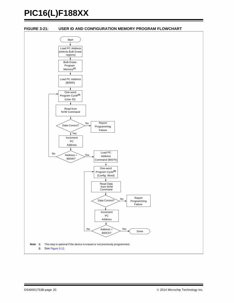
FIGURE 3-21: USER ID AND CONFIGURATION MEMORY PROGRAM FLOWCHART
Start
Load PC Address
Program Cycle(2)
Read fromNVM Command
Data Correct?Report
ProgrammingFailure
Address =8004h?
Data Correct?Report
ProgrammingFailure
No
Yes
Yes
No
IncrementPC
Address
No Load PCAddress
Command (8007h)
Done
One-word
One-wordProgram Cycle(2)
(Config. Word)
(User ID)
Read Data
Commandfrom NVM
ProgramBulk Erase
Memory(1)
Yes
IncrementPC
Address
Note 1: This step is optional if the device is erased or not previously programmed.
2: See Figure 3-12.
Address =800Ch?
No
regions)(selects Bulk Erase
Load PC Address(8000h)
DS40001753B-page 20 2014 Microchip Technology Inc.

PIC16(L)F188XX
FIGURE 3-22: BULK ERASE FLOWCHART
3.3 Code Protection
Code protection is controlled using the CP bit. When code protection is enabled, all program memory locations(0000h-7FFFh) read as ‘0’. Further programming is disabled for the program memory (0000h-7FFFh), until the next bulkerase operation is performed. Program memory can still be programmed and read during program execution.
The user ID locations and Configuration Words can be programmed and read out regardless of the code protectionsettings.
3.3.1 PROGRAM MEMORY
Code protection is enabled by programming the CP bit to ‘0’. The only way to disable code protection is to use the BulkErase Memory command (with the PC set to an address so as to Bulk Erase all program Flash contents).
3.3.2 DATA MEMORY
Data memory protection is enabled by programming the CPD bit to '0'. The only way to disable code protection is to usethe Bulk Erase Memory command.
Start
Load PC Address
Done
Bulk EraseProgram Memory
(determines region(s) that will get erased)
Wait TERAB forOperation to Complete
2014 Microchip Technology Inc. DS40001753B-page 21
PIC16(L)F188XX
3.4 Hex File Usage
In the hex file there are two bytes per program word stored in the Intel® INHX32 hex format. Data is stored LSB first,MSB second. Because there are two bytes per word, the addresses in the hex file are 2x the address in programmemory. For example, if the Configuration Word 1 is stored at 8007h, in the hex file this will be referenced as1000Eh-1000Fh.
3.4.1 CONFIGURATION WORD
To allow portability of code, it is strongly recommended that the programmer is able to read the Configuration Wordsand user ID locations from the hex file. If the Configuration Words information was not present in the hex file, a simplewarning message may be issued. Similarly, while saving a hex file, Configuration Words and user ID information shouldbe included.
3.4.2 DEVICE ID
If a device ID is present in the hex file at 1000Ch-1000Dh (8006h on the part), the programmer should verify the deviceID against the value read from the part. On a mismatch condition, the programmer should generate a warning message.
3.4.3 CHECKSUM COMPUTATION
The checksum is calculated by two different methods dependent on the setting of the CP Configuration bit. Refer toAppendix B: “PIC16(L)F188XX Device ID, Checksums and Pinout Descriptions” for checksum computation exam-ples.
3.4.3.1 Program Code Protection Disabled
With the program code protection disabled, the checksum is computed by reading the contents of the program memorylocations and adding up the program memory data starting at address 0000h, up to the maximum user addressablelocation (e.g., 0FFFh). Any Carry bits exceeding 16 bits are ignored. Additionally, the relevant bits of the ConfigurationWords are added to the checksum. All unimplemented Configuration bits are masked to ‘0’.
3.4.3.2 Program Code Protection Enabled
When the MPLAB® IDE check box for ConfigureID Memory... Use Unprotected Checksum is checked, then the16-bit checksum of the equivalent unprotected device is computed and stored in the user ID. Each nibble of theunprotected checksum is stored in the Least Significant nibble of each of the four user ID locations. The MostSignificant checksum nibble is stored in the user ID at location 8000h, the second Most Significant nibble is stored atlocation 8001h, and so forth for the remaining nibbles and ID locations.
The checksum of a code-protected device is computed in the following manner: the Least Significant nibble of each userID is used to create a 16-bit value. The Least Significant nibble of user ID location 8000h is the Most Significant nibbleof the 16-bit value. The Least Significant nibble of user ID location 8001h is the second Most Significant nibble, and soforth for the remaining user IDs and 16-bit value nibbles. The resulting 16-bit value is summed with the ConfigurationWords. All unimplemented Configuration bits are masked to ‘0’.
DS40001753B-page 22 2014 Microchip Technology Inc.

PIC16(L)F188XX
3.5 Electrical Specifications
Refer to device-specific data sheet for absolute maximum ratings.
TABLE 3-3: AC/DC CHARACTERISTICS TIMING REQUIREMENTS FOR PROGRAM/VERIFY MODE
AC/DC CHARACTERISTICSStandard Operating ConditionsProduction tested at 25°C
Sym. Characteristics Min. Typ. Max. Units Conditions/Comments
Programming Supply Voltages and Currents
VDDSupply Voltage (VDDMIN(1), VDDMAX)
PICXXLF1XXXX 1.80 — 3.60 V
PICXXF1XXXX 2.30 — 5.50 V
VPEW Read/Write and Row Erase operations VDDMIN — VDDMAX V
VBE Bulk Erase operations VBOR(2) — VDDMAX V
IDDI Current on VDD, Idle — — 1.0 mA
IDDP Current on VDD, Programming — — 5.0 mA
IPP
VPP
Current on MCLR/VPP — — 600 A
VIHHHigh voltage on MCLR/VPP for Program/Verify mode entry
8.0 — 9.0 V
TVHHRMCLR rise time (VIL to VIHH) for Program/Verify mode entry
— — 1.0 s
I/O pins
VIH (ICSPCLK, ICSPDAT, MCLR/VPP) input high level 0.8 VDD — — V
VIL (ICSPCLK, ICSPDAT, MCLR/VPP) input low level — — 0.2 VDD V
VOH
ICSPDAT output high level VDD-0.7VDD-0.7VDD-0.7
— — VIOH = 3.5 mA, VDD = 5VIOH = 3 mA, VDD = 3.3VIOH = 1 mA, VDD = 1.8V
VOL
ICSPDAT output low level— —
VSS+0.6VSS+0.6VSS+0.6
VIOL = 8 mA, VDD = 5VIOL = 6 mA, VDD = 3.3VIOL = 1.8 mA, VDD = 1.8V
Programming Mode Entry and Exit
TENTSPrograming mode entry setup time: ICSPCLK, ICSPDAT setup time before VDD or MCLR
100 — — ns
TENTHPrograming mode entry hold time: ICSPCLK, ICSPDAT hold time after VDD or MCLR
250 — — s
Serial Program/Verify
TCKL Clock Low Pulse Width 100 — — ns
TCKH Clock High Pulse Width 100 — — ns
TDS Data in setup time before clock 100 — — ns
TDH Data in hold time after clock 100 — — ns
TCOClock to data out valid (during a Read Data command)
0 — 80 ns
Note 1: Bulk-erased devices default to brown-out enabled, with BORV = 1 (low trip point). VDDMIN is the VBOR threshold (with BORV = 1) when performing low-voltage programming on a bulk-erased device, to ensure that the device is not held in Brown-out Reset.
2: The hardware requires VDD to be above the BOR threshold, at the ~2.4V nominal setting, in order to perform Bulk Erase operations. This threshold does not depend on the BORV Configuration bit settings. The threshold is the same for both F and LF devices, even though the LF devices may not have a user configurable ~2.4V nominal BOR trip point setting. Refer to the microcontroller device data sheet specifications for min./typ./max. limits of the VBOR level (at the BORV = 0 setting of F devices).
3: Externally timed writes are not supported for Configuration bits.
2014 Microchip Technology Inc. DS40001753B-page 23

PIC16(L)F188XX
TLZDClock to data low-impedance (during a Read Data command)
0 — 80 ns
THZDClock to data high-impedance (during a Read Data command)
0 — 80 ns
TDLY
Data input not driven to next clock input (delay required between command/data or command/command)
1.0 — — s
TERAB Bulk Erase cycle time
— — 5.6 msPIC16(L)F18854, PIC16(L)F188x5
— — 8.4 ms PIC16(L)F188x6
— — 14 ms PIC16(L)F188x7
TERAR Row Erase cycle time — — 2.8 ms
TPINT Internally timed programming operation time——
——
2.85.6
msms
Program memory Configuration Words
TPEXT
Delay required between Begin Externally Timed Programming and End Externally Timed Programming commands
1.0 — 2.1 ms (Note 3)
TDISDelay required after End Externally Timed Programming command
300 — — s
TEXIT Time delay when exiting Program/Verify mode 1 — — s
TABLE 3-3: AC/DC CHARACTERISTICS TIMING REQUIREMENTS FOR PROGRAM/VERIFY MODE (CONTINUED)
AC/DC CHARACTERISTICSStandard Operating ConditionsProduction tested at 25°C
Sym. Characteristics Min. Typ. Max. Units Conditions/Comments
Note 1: Bulk-erased devices default to brown-out enabled, with BORV = 1 (low trip point). VDDMIN is the VBOR threshold (with BORV = 1) when performing low-voltage programming on a bulk-erased device, to ensure that the device is not held in Brown-out Reset.
2: The hardware requires VDD to be above the BOR threshold, at the ~2.4V nominal setting, in order to perform Bulk Erase operations. This threshold does not depend on the BORV Configuration bit settings. The threshold is the same for both F and LF devices, even though the LF devices may not have a user configurable ~2.4V nominal BOR trip point setting. Refer to the microcontroller device data sheet specifications for min./typ./max. limits of the VBOR level (at the BORV = 0 setting of F devices).
3: Externally timed writes are not supported for Configuration bits.
DS40001753B-page 24 2014 Microchip Technology Inc.
PIC16(L)F188XX
APPENDIX A: REVISION HISTORY
Revision A (06/2014)
Initial release of the document.
Revision B (12/2014)
Added Sections 3.1.3.6 and 3.1.3.7.
Updated Appendix B.
Updated Example B-1, B-2, B-3 and B-4.
Updated Figures 2-1, 3-1, 3-2, 3-18, and 3-19.
Updated Register B-4.
Updated Sections 1.2.2, 1.2.3, 3.1.1.1, 3.1.1.2, 3.1.1.3,3.1.3.1, and 3.2.
Updated Table 3-1, 3-2, and 3-3.
2014 Microchip Technology Inc. DS40001753B-page 25

PIC
16(L)F
188XX
DS
40
00
17
53
B-p
ag
e 2
6
20
14
Micro
chip
Te
chn
olo
gy In
c.
NS
Checksum
Mask (HEX)
Unprotected Code-protected
Blank (HEX)
00AAh First and Last
(HEX)
Blank (HEX)
00AAh First and Last
(HEX)
0003 C7DF 4935 9FBB 2111
0003 C7DF 4935 9FBB 2111
0003 B7DF 3935 8FBB 1111
0003 B7DF 3935 8FBB 1111
0003 B7DF 3935 8FBB 1111
0003 B7DF 3935 8FBB 1111
0003 97DF 1935 6FBB F111
0003 97DF 1935 6FBB F111
0003 97DF 1935 6FBB F111
0003 97DF 1935 6FBB F111
0003 57DF D935 2FBB B111
0003 57DF D935 2FBB B111
0003 57DF D935 2FBB B111
0003 57DF D935 2FBB B111
APPENDIX B: PIC16(L)F188XX DEVICE ID, CHECKSUMS AND PINOUT DESCRIPTIO
TABLE B-1: DEVICE IDs AND CHECKSUMS
DeviceDevice
ID
Config. 1 Config. 2 Config. 3 Config. 4 Config. 5
Word (HEX)
Mask (HEX)
Word (HEX)
Mask (HEX)
Word (HEX)
Mask (HEX)
Word (HEX)
Mask (HEX)
Unprotected Word (HEX)
Protected Word (HEX)
PIC16F18854 306Ah 3FFF 2977 3FFF 3EE3 3FFF 3F7F 3FFF 3003 3FFF 3FFC
PIC16LF18854 306Bh 3FFF 2977 3FFF 3EE3 3FFF 3F7F 3FFF 3003 3FFF 3FFC
PIC16F18855 306Ch 3FFF 2977 3FFF 3EE3 3FFF 3F7F 3FFF 3003 3FFF 3FFC
PIC16F18875 306Dh 3FFF 2977 3FFF 3EE3 3FFF 3F7F 3FFF 3003 3FFF 3FFC
PIC16LF18855 306Eh 3FFF 2977 3FFF 3EE3 3FFF 3F7F 3FFF 3003 3FFF 3FFC
PIC16LF18875 306Fh 3FFF 2977 3FFF 3EE3 3FFF 3F7F 3FFF 3003 3FFF 3FFC
PIC16F18856 3070h 3FFF 2977 3FFF 3EE3 3FFF 3F7F 3FFF 3003 3FFF 3FFC
PIC16F18876 3071h 3FFF 2977 3FFF 3EE3 3FFF 3F7F 3FFF 3003 3FFF 3FFC
PIC16LF18856 3072h 3FFF 2977 3FFF 3EE3 3FFF 3F7F 3FFF 3003 3FFF 3FFC
PIC16LF18876 3073h 3FFF 2977 3FFF 3EE3 3FFF 3F7F 3FFF 3003 3FFF 3FFC
PIC16F18857 3074h 3FFF 2977 3FFF 3EE3 3FFF 3F7F 3FFF 3003 3FFF 3FFC
PIC16F18877 3075h 3FFF 2977 3FFF 3EE3 3FFF 3F7F 3FFF 3003 3FFF 3FFC
PIC16LF18857 3076h 3FFF 2977 3FFF 3EE3 3FFF 3F7F 3FFF 3003 3FFF 3FFC
PIC16LF18877 3077h 3FFF 2977 3FFF 3EE3 3FFF 3F7F 3FFF 3003 3FFF 3FFC

PIC16(L)F188XX
EXAMPLE B-1: CHECKSUM COMPUTED WITH PROGRAM CODE PROTECTION DISABLED PIC16F18854, BLANK DEVICE
EXAMPLE B-2: CHECKSUM COMPUTED WITH PROGRAM CODE PROTECTION DISABLED PIC16F18854, 00AAh AT FIRST AND LAST ADDRESS
PIC16F18854 Sum of Memory addresses 0000h-0FFFh F000h (1000h*3FFFh)Configuration Word 1 3FFFhConfiguration Word 1 mask 2977hConfiguration Word 2 3FFFhConfiguration Word 2 mask 3EE3hConfiguration Word 3 3FFFhConfiguration Word 3 mask 3F7FhConfiguration Word 4 3FFFhConfiguration Word 4 mask 3003hConfiguration Word 5 Unprotected 3FFFhConfiguration Word 5 mask 0003hChecksum = F000h + (3FFFh and 2977h) + (3FFFh and 3EE3h) + (3FFFh and 3F7Fh) +
(3FFFh and 3003h) + (3FFFh and 0003h)= F000h + 2977h + 3EE3h + 3F7Fh + 3003h + 0003h= C7DFh
PIC16F18854 Sum of Memory addresses 0000h-0FFFh 7156h (AAh + (FFEh*3FFFh) + AAh)Configuration Word 1 3FFFhConfiguration Word 1 mask 2977hConfiguration Word 2 3FFFhConfiguration Word 2 mask 3EE3hConfiguration Word 3 3FFFhConfiguration Word 3 mask 3F7FhConfiguration Word 4 3FFFhConfiguration Word 4 mask 3003hConfiguration Word 5 Unprotected 3FFFhConfiguration Word 5 mask 0003hChecksum = 7156h + (3FFFh and 2977h) + (3FFFh and 3EE3h) + (3FFFh and 3F7Fh) +
(3FFFh and 3003h) + (3FFFh and 0003h)= 7156h + 2977h + 3EE3h + 3F7Fh + 3003h + 0003h= 4935h
2014 Microchip Technology Inc. DS40001753B-page 27

PIC16(L)F188XX
EXAMPLE B-3: CHECKSUM COMPUTED WITH PROGRAM CODE PROTECTION ENABLED PIC16F18854, BLANK DEVICE
EXAMPLE B-4: CHECKSUM COMPUTED WITH PROGRAM CODE PROTECTION ENABLED PIC16F18854, 00AAh AT FIRST AND LAST ADDRESS
PIC16F18854 Configuration Word 1 3FFFhConfiguration Word 1 mask 2977hConfiguration Word 2 3FFFhConfiguration Word 2 mask 3EE3hConfiguration Word 3 3FFFhConfiguration Word 3 mask 3F7FhConfiguration Word 4 3FFFhConfiguration Word 4 mask 3003hConfiguration Word 5 Unprotected 3FFChConfiguration Word 5 mask 0003hSum of User IDs = (000Ch and 000Fh) << 12 + (0007h and 000Fh) << 8 + (000Dh and 000Fh)
<< 4 + (000Fh and 000Fh)= C000h + 0700h + 00D0h + 000Fh= C7DFh
Checksum = (3FFFh and 2977h) + (3FFFh and 3EE3h) + (3FFFh and 3F7Fh) + (3FFFh and 3003h) + (3FFCh and 0003h) + C7DFh
= 2977h + 3EE3h + 3F7Fh + 3003h + 0000h + C7DFh= 9FBBh
PIC16F18854 Configuration Word 1 3FFFhConfiguration Word 1 mask 2977hConfiguration Word 2 3FFFhConfiguration Word 2 mask 3EE3hConfiguration Word 3 3FFFhConfiguration Word 3 mask 3F7FhConfiguration Word 4 3FFFhConfiguration Word 4 mask 3003hConfiguration Word 5 Unprotected 3FFChConfiguration Word 5 mask 0003hSum of User IDs = (0004h and 000Fh) << 12 + (0009h and 000Fh) << 8 + (0003h and 000Fh)
<< 4 + (0005h and 000Fh)= 4000h + 0900h + 0030h + 0005h= 4935h
Checksum = (3FFFh and 2977h) + (3FFFh and 3EE3h) + (3FFFh and 3F7Fh) + (3FFFh and 3003h) + (3FFCh and 0003h) + 4935h
= 2977h + 3EE3h + 3F7Fh + 3003h + 0000h + 4935h= 2111h
DS40001753B-page 28 2014 Microchip Technology Inc.

PIC16(L)F188XX
TABLE B-2: PROGRAMMING PIN LOCATIONS BY PACKAGE TYPE
Device PackagePackage
Code
Package Drawing
Number(1)
VDD VSS MCLR ICSPCLK ICSPDAT
PIN PIN PIN PORT PIN PORT PIN PORT
PIC16(L)F18854 28-pin SPDIP (SP) C04-070 20 19, 8 1 RE3 27 RB6 28 RB7
28-pin SSOP (SS) C04-073 20 19, 8 1 RE3 27 RB6 28 RB7
28-pin SOIC (SO) C04-052 20 19, 8 1 RE3 27 RB6 28 RB7
28-pin UQFN (MV) C04-152 17 16, 5 26 RE3 24 RB6 25 RB7
PIC16(L)F18855 28-pin SPDIP (SP) C04-070 20 19, 8 1 RE3 27 RB6 28 RB7
28-pin SSOP (SS) C04-073 20 19, 8 1 RE3 27 RB6 28 RB7
28-pin SOIC (SO) C04-052 20 19, 8 1 RE3 27 RB6 28 RB7
28-pin UQFN (MV) C04-152 17 16, 5 26 RE3 24 RB6 25 RB7
PIC16(L)F18875 40-pin PDIP (P) C04-016 32, 11 31, 12 1 RE3 39 RB6 40 RB7
44-pin TQFP (PT) C04-076 28, 7 6 18 RE3 16 RB6 17 RB7
40-pin UQFN (MV) C04-156 26, 7 27, 6 16 RE3 14 RB6 15 RB7
PIC16(L)F18856 28-pin SPDIP (SP) C04-070 20 19, 8 1 RE3 27 RB6 28 RB7
28-pin SSOP (SS) C04-073 20 19, 8 1 RE3 27 RB6 28 RB7
28-pin SOIC (SO) C04-052 20 19, 8 1 RE3 27 RB6 28 RB7
28-pin UQFN (MV) C04-152 17 16, 5 26 RE3 24 RB6 25 RB7
28-pin QFN (ML) C04-105 17 16, 5 26 RE3 24 RB6 25 RB7
PIC16(L)F18876 40-pin PDIP (P) C04-016 32, 11 31, 12 1 RE3 39 RB6 40 RB7
44-pin TQFP (PT) C04-076 28, 7 6 18 RE3 16 RB6 17 RB7
40-pin UQFN (MV) C04-156 26, 7 27, 6 16 RE3 14 RB6 15 RB7
44-pin QFN (ML) C04-103 28, 8, 7 6 18 RE3 16 RB6 17 RB7
PIC16(L)F18857 28-pin SPDIP (SP) C04-070 20 19, 8 1 RE3 27 RB6 28 RB7
28-pin SSOP (SS) C04-073 20 19, 8 1 RE3 27 RB6 28 RB7
28-pin SOIC (SO) C04-052 20 19, 8 1 RE3 27 RB6 28 RB7
28-pin QFN (ML) C04-105 17 16, 5 26 RE3 24 RB6 25 RB7
PIC16(L)F18877 40-pin PDIP (P) C04-016 32, 11 31, 12 1 RE3 39 RB6 40 RB7
44-pin TQFP (PT) C04-076 28, 7 6 18 RE3 16 RB6 17 RB7
40-pin UQFN (MV) C04-156 26, 7 27, 6 16 RE3 14 RB6 15 RB7
44-pin QFN (ML) C04-103 28, 8, 7 6 18 RE3 16 RB6 17 RB7
Note 1: The most current package drawings can be found in the Microchip Packaging Specification, DS00049, found at http://www.microchip.com/packaging. The drawing numbers listed above do not include the current revision designator which is added at the end of the number.
2014 Microchip Technology Inc. DS40001753B-page 29

PIC16(L)F188XX
REGISTER B-1: CONFIGURATION WORD 1: OSCILLATORSR/P-1 U-1 R/P-1 U-1 U-1 R/P-1 U-1 R/P-1 R/P-1 R/P-1 U-1 R/P-1 R/P-1 R/P-1
FCMEN — CSWEN — — CLKOUTEN — RSTOSC2 RSTOSC1 RSTOSC0 — FEXTOSC2 FEXTOSC1 FEXTOSC0
bit 13 bit 0
Legend:
R = Readable bit P = Programmable bit U = Unimplemented bit, read as ‘1’ x = Bit is unknown
‘0’ = Bit is cleared ‘1’ = Bit is set n = Value when blank or after Bulk Erase W = Writable bit
bit 13 FCMEN: Fail-Safe Clock Monitor Enable bit 1 = FSCM timer enabled0 = FSCM timer disabled
bit 12 Unimplemented: Read as ‘1’
bit 11 CSWEN: Clock Switch Enable bit1 = Writing to NOSC and NDIV is allowed0 = The NOSC and NDIV bits cannot be changed by user software
bit 10-9 Unimplemented: Read as ‘1’
bit 8 CLKOUTEN: Clock Out Enable bitIf FEXTOSC = EC (high, mid or low) or Not Enabled:1 = CLKOUT function is disabled; I/O or oscillator function on OSC20 = CLKOUT function is enabled; FOSC/4 clock appears at OSC2Otherwise:This bit is ignored.
bit 7 Unimplemented: Read as ‘1’
bit 6-4 RSTOSC<2:0>: Power-up default value for COSC bitsThis value is the Reset-default value for COSC and selects the oscillator first used by user software.111 = EXTOSC operating per FEXTOSC bits (device manufacturing default) 110 = HFINTOSC with HFFRQ = 4’b0000101 = Reserved100 = LFINTOSC011 = SOSC010 = EXTOSC with 2x PLL, with EXTOSC operating per FEXTOSC bits001 = EXTOSC with 4x PLL, with EXTOSC operating per FEXTOSC bits000 = HFINTOSC with 2x PLL and HFFRQ = 4’b1111
bit 3 Unimplemented: Read as ‘1’
bit 2-0 FEXTOSC<2:0>:FEXTOSC External Oscillator mode Selection bits111 = EC (External Clock) above 8 MHz; PFM set to high power (device manufacturing default)110 = EC (External Clock) for 100 kHz to 8 MHz; PFM set to medium power101 = EC (External Clock) below 100 kHz; PFM set to low power100 = Oscillator not enabled011 = Reserved (do not use)010 = HS (Crystal oscillator) above 4 MHz; PFM set to high power001 = XT (Crystal oscillator) above 100 kHz, below 4 MHz; PFM set to medium power000 = LP (Crystal oscillator) optimized for 32.768 kHz; PFM set to low power
DS40001753B-page 30 2014 Microchip Technology Inc.

PIC16(L)F188XX
REGISTER B-2: CONFIGURATION WORD 2: SUPERVISORSR/P-1 R/P-1 R/P-1 R/P-1 R/P-1 U-1 R/P-1 R/P-1 R/P-1 U-1 U-1 U-1 R/P-1 R/P-1
DEBUG STVREN PPS1WAY ZCDDIS BORV — BOREN1 BOREN0 LPBOREN — — — PWRTE MCLRE
bit 13 bit 0
Legend:
R = Readable bit P = Programmable bit U = Unimplemented bit, read as ‘1’ x = Bit is unknown
‘0’ = Bit is cleared ‘1’ = Bit is set n = Value when blank or after Bulk Erase W = Writable bit
bit 13 DEBUG: Debugger Enable bit 1 = Background debugger disabled0 = Background debugger enabled
bit 12 STVREN: Stack Overflow/Underflow Reset Enable bit1 = Stack Overflow or Underflow will cause a Reset0 = Stack Overflow or Underflow will not cause a Reset
bit 11 PPS1WAY: PPSLOCK One-Way Set Enable bit1 = The PPSLOCK bit can be cleared and set only once; PPS registers remain locked after one clear/set cycle0 = The PPSLOCK bit can be set and cleared repeatedly (subject to the unlock sequence)
bit 10 ZCDDIS: Zero-Cross Detect Disable bit1 = ZCD disabled. ZCD can be enabled by setting the ZCDSEN bit of the ZCDCON register0 = ZCD always enabled (ZCDSEN bit is ignored)
bit 9 BORV: Brown-out Reset Voltage Selection bit1 = Brown-out Reset voltage (VBOR) set to lower trip point level 0 = Brown-out Reset voltage (VBOR) set to higher trip point levelThe higher voltage setting is recommended for operation at or above 16 MHz.
bit 8 Unimplemented: Read as ‘1’
bit 7-6 BOREN<1:0>: Brown-out Reset Enable bitsWhen enabled, Brown-out Reset Voltage (VBOR) is set by the BORV bit11 = Brown-out Reset is enabled; SBOREN bit is ignored10 = Brown-out Reset is enabled while running, disabled in Sleep; SBOREN bit is ignored01 = Brown-out Reset is enabled according to SBOREN00 = Brown-out Reset is disabled
bit 5 LPBOREN: Low-Power BOR Enable bit1 = ULPBOR is disabled0 = ULPBOR is enabled
bit 4-2 Unimplemented: Read as ‘1’
bit 1 PWRTE: Power-up Timer Enable bit 1 = PWRT is disabled0 = PWRT is enabled
bit 0 MCLRE: Master Clear (MCLR) Enable bit If LVP = 1:RE3 pin function is MCLR (it will reset device when driven low)If LVP = 0:1 = MCLR pin is MCLR (it will reset device when driven low)0 = MCLR pin may be used as general purpose RE3 input
2014 Microchip Technology Inc. DS40001753B-page 31

PIC16(L)F188XX
REGISTER B-3: CONFIGURATION WORD 3: WINDOWED WATCHDOG
R/P-1 R/P-1 R/P-1 R/P-1 R/P-1 R/P-1
WDTCCS2 WDTCCS1 WDTCCS0 WDTCWS2 WDTCWS1 WDTCWS0
bit 13 bit 8
U-1 R/P-1 R/P-1 R/P-1 R/P-1 R/P-1 R/P-1 R/P-1
WDTE1 WDTE0 WDTCPS4 WDTCPS3 WDTCPS2 WDTCPS1 WDTCPS0
bit 7 bit 0
Legend:
R = Readable bit P = Programmable bit x = Bit is unknown U = Unimplemented bit, read as ‘1’
‘0’ = Bit is cleared ‘1’ = Bit is set W = Writable bit n = Value when blank or after Bulk Erase
bit 13-11 WDTCCS<2:0>: WDT input clock selector.000 = WDT reference clock is the 31.25 kHz HFINTOSC (MFINTOSC) output001 = WDT reference clock is the 31.0 kHz LFINTOSC (default value)010 = Reserved....110 = Reserved111 = Software Control
bit 10-8 WDTCWS<2:0>: WDT Window Select bits
bit 7 Unimplemented: Read as ‘1’
bit 6-5 WDTE<1:0>: WDT Operating mode:00 = WDT disabled, SWDTEN is ignored01 = WDT enabled/disabled by SWDTEN bit in WDTCON010 = WDT enabled while Sleep = 0, suspended when Sleep = 1; SWDTEN ignored11 = WDT enabled regardless of Sleep; SWDTEN is ignored
WDTCWS
WDTWS at PORSoftware control of WDTWS?
Keyed access
required?ValueWindow delay
Percent of time
Window opening
Percent of time
000 000 87.5 12.5
No Yes
001 001 75 25
010 010 62.5 37.5
011 011 50 50
100 100 37.5 62.5
101 101 25 75
110 111 n/a 100
111 111 n/a 100 Yes No
DS40001753B-page 32 2014 Microchip Technology Inc.

PIC16(L)F188XX
bit 4-0 WDTCPS<4:0>: WDT Period Select bits
REGISTER B-3: CONFIGURATION WORD 3: WINDOWED WATCHDOG (CONTINUED)
WDTCPS
WDTPS at PORSoftware control
of WDTPS?Value Divider RatioTypical time out
(FIN = 31 kHz)
00000 00000 1:32 25 1 ms
No
00001 00001 1:64 26 2 ms
00010 00010 1:128 27 4 ms
00011 00011 1:256 28 8 ms
00100 00100 1:512 29 16 ms
00101 00101 1:1024 210 32 ms
00110 00110 1:2048 211 64 ms
00111 00111 1:4096 212 128 ms
01000 01000 1:8192 213 256 ms
01001 01001 1:16384 214 512 ms
01010 01010 1:32768 215 1 s
01011 01011 1:65536 216 2 s
01100 01100 1:131072 217 4 s
01101 01101 1:262144 218 8 s
01110 01110 1:524299 219 16 s
01111 01111 1:1048576 220 32 s
10000 10000 1:2097152 221 64 s
10001 10001 1:4194304 222 128 s
10010 10010 1:8388608 223 256 s
10011...11110
10011...11110
1:32 25 1 ms No
2014 Microchip Technology Inc. DS40001753B-page 33
PIC16(L)F188XX
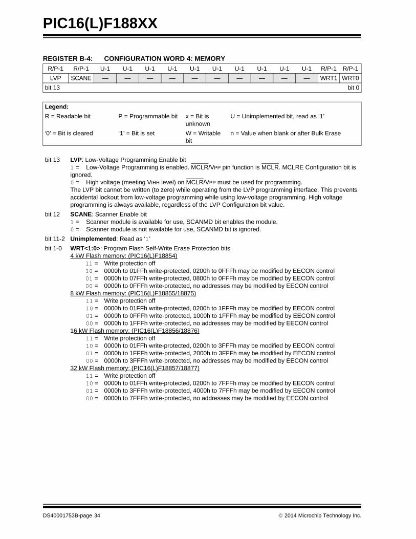
REGISTER B-4: CONFIGURATION WORD 4: MEMORY
R/P-1 R/P-1 U-1 U-1 U-1 U-1 U-1 U-1 U-1 U-1 U-1 U-1 R/P-1 R/P-1
LVP SCANE — — — — — — — — — — WRT1 WRT0
bit 13 bit 0
Legend:
R = Readable bit P = Programmable bit x = Bit is unknown
U = Unimplemented bit, read as ‘1’
‘0’ = Bit is cleared ‘1’ = Bit is set W = Writable bit
n = Value when blank or after Bulk Erase
bit 13 LVP: Low-Voltage Programming Enable bit1 = Low-Voltage Programming is enabled. MCLR/VPP pin function is MCLR. MCLRE Configuration bit is ignored.0 = High voltage (meeting VIHH level) on MCLR/VPP must be used for programming.The LVP bit cannot be written (to zero) while operating from the LVP programming interface. This prevents accidental lockout from low-voltage programming while using low-voltage programming. High voltage programming is always available, regardless of the LVP Configuration bit value.
bit 12 SCANE: Scanner Enable bit1 = Scanner module is available for use, SCANMD bit enables the module.0 = Scanner module is not available for use, SCANMD bit is ignored.
bit 11-2 Unimplemented: Read as ‘1’
bit 1-0 WRT<1:0>: Program Flash Self-Write Erase Protection bits4 kW Flash memory: (PIC16(L)F18854)
11 = Write protection off10 = 0000h to 01FFh write-protected, 0200h to 0FFFh may be modified by EECON control01 = 0000h to 07FFh write-protected, 0800h to 0FFFh may be modified by EECON control00 = 0000h to 0FFFh write-protected, no addresses may be modified by EECON control
8 kW Flash memory: (PIC16(L)F18855/18875)11 = Write protection off10 = 0000h to 01FFh write-protected, 0200h to 1FFFh may be modified by EECON control01 = 0000h to 0FFFh write-protected, 1000h to 1FFFh may be modified by EECON control00 = 0000h to 1FFFh write-protected, no addresses may be modified by EECON control
16 kW Flash memory: (PIC16(L)F18856/18876)11 = Write protection off10 = 0000h to 01FFh write-protected, 0200h to 3FFFh may be modified by EECON control01 = 0000h to 1FFFh write-protected, 2000h to 3FFFh may be modified by EECON control00 = 0000h to 3FFFh write-protected, no addresses may be modified by EECON control
32 kW Flash memory: (PIC16(L)F18857/18877)11 = Write protection off10 = 0000h to 01FFh write-protected, 0200h to 7FFFh may be modified by EECON control01 = 0000h to 3FFFh write-protected, 4000h to 7FFFh may be modified by EECON control00 = 0000h to 7FFFh write-protected, no addresses may be modified by EECON control
DS40001753B-page 34 2014 Microchip Technology Inc.
PIC16(L)F188XX
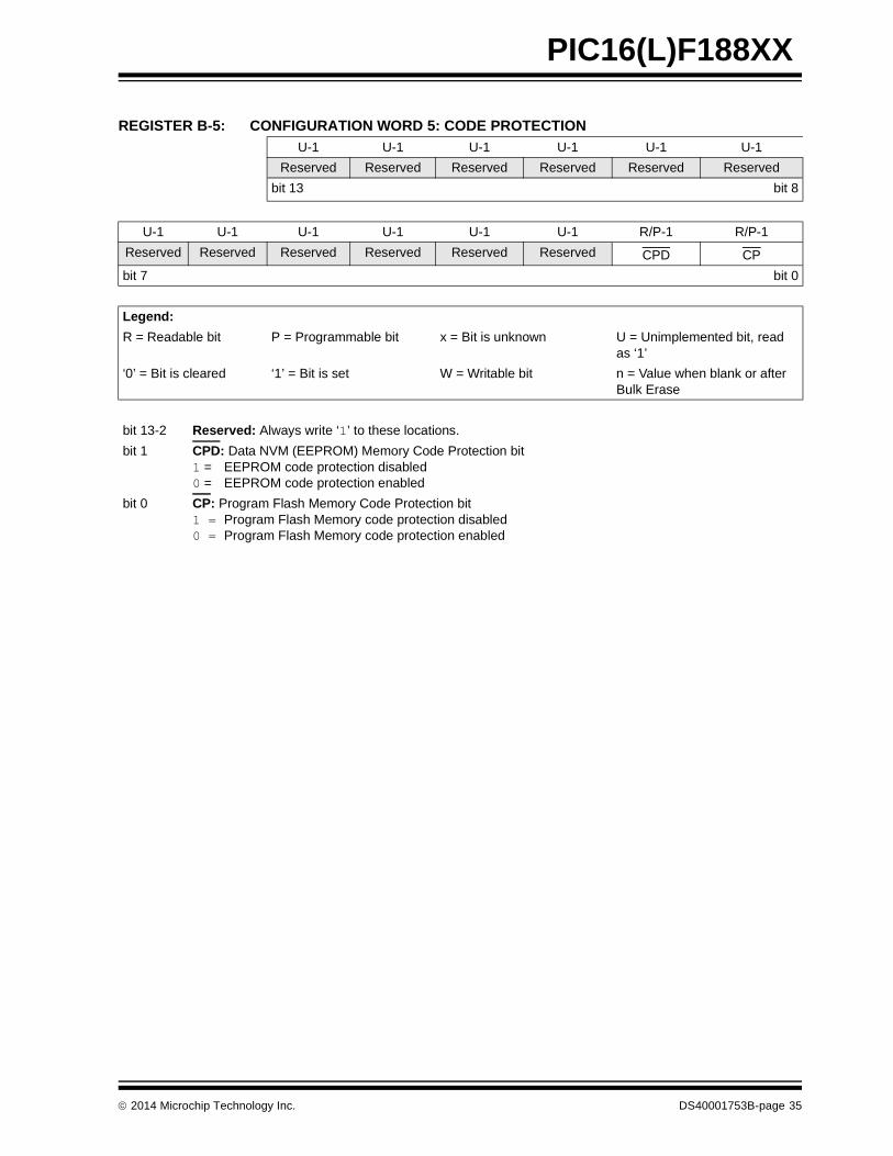
REGISTER B-5: CONFIGURATION WORD 5: CODE PROTECTION
U-1 U-1 U-1 U-1 U-1 U-1
Reserved Reserved Reserved Reserved Reserved Reserved
bit 13 bit 8
U-1 U-1 U-1 U-1 U-1 U-1 R/P-1 R/P-1
Reserved Reserved Reserved Reserved Reserved Reserved CPD CP
bit 7 bit 0
Legend:
R = Readable bit P = Programmable bit x = Bit is unknown U = Unimplemented bit, read as ‘1’
‘0’ = Bit is cleared ‘1’ = Bit is set W = Writable bit n = Value when blank or after Bulk Erase
bit 13-2 Reserved: Always write ‘1’ to these locations.
bit 1 CPD: Data NVM (EEPROM) Memory Code Protection bit1 = EEPROM code protection disabled0 = EEPROM code protection enabled
bit 0 CP: Program Flash Memory Code Protection bit1 = Program Flash Memory code protection disabled0 = Program Flash Memory code protection enabled
2014 Microchip Technology Inc. DS40001753B-page 35

PIC16(L)F188XX
NOTES:
DS40001753B-page 36 2014 Microchip Technology Inc.

Note the following details of the code protection feature on Microchip devices:
• Microchip products meet the specification contained in their particular Microchip Data Sheet.
• Microchip believes that its family of products is one of the most secure families of its kind on the market today, when used in the intended manner and under normal conditions.
• There are dishonest and possibly illegal methods used to breach the code protection feature. All of these methods, to our knowledge, require using the Microchip products in a manner outside the operating specifications contained in Microchip’s Data Sheets. Most likely, the person doing so is engaged in theft of intellectual property.
• Microchip is willing to work with the customer who is concerned about the integrity of their code.
• Neither Microchip nor any other semiconductor manufacturer can guarantee the security of their code. Code protection does not mean that we are guaranteeing the product as “unbreakable.”
Code protection is constantly evolving. We at Microchip are committed to continuously improving the code protection features of ourproducts. Attempts to break Microchip’s code protection feature may be a violation of the Digital Millennium Copyright Act. If such actsallow unauthorized access to your software or other copyrighted work, you may have a right to sue for relief under that Act.
Information contained in this publication regarding deviceapplications and the like is provided only for your convenienceand may be superseded by updates. It is your responsibility toensure that your application meets with your specifications.MICROCHIP MAKES NO REPRESENTATIONS ORWARRANTIES OF ANY KIND WHETHER EXPRESS ORIMPLIED, WRITTEN OR ORAL, STATUTORY OROTHERWISE, RELATED TO THE INFORMATION,INCLUDING BUT NOT LIMITED TO ITS CONDITION,QUALITY, PERFORMANCE, MERCHANTABILITY ORFITNESS FOR PURPOSE. Microchip disclaims all liabilityarising from this information and its use. Use of Microchipdevices in life support and/or safety applications is entirely atthe buyer’s risk, and the buyer agrees to defend, indemnify andhold harmless Microchip from any and all damages, claims,suits, or expenses resulting from such use. No licenses areconveyed, implicitly or otherwise, under any Microchipintellectual property rights.
2014 Microchip Technology Inc.
QUALITY MANAGEMENT SYSTEM CERTIFIED BY DNV
== ISO/TS 16949 ==
Trademarks
The Microchip name and logo, the Microchip logo, dsPIC, FlashFlex, flexPWR, JukeBlox, KEELOQ, KEELOQ logo, Kleer, LANCheck, MediaLB, MOST, MOST logo, MPLAB, OptoLyzer, PIC, PICSTART, PIC32 logo, RightTouch, SpyNIC, SST, SST Logo, SuperFlash and UNI/O are registered trademarks of Microchip Technology Incorporated in the U.S.A. and other countries.
The Embedded Control Solutions Company and mTouch are registered trademarks of Microchip Technology Incorporated in the U.S.A.
Analog-for-the-Digital Age, BodyCom, chipKIT, chipKIT logo, CodeGuard, dsPICDEM, dsPICDEM.net, ECAN, In-Circuit Serial Programming, ICSP, Inter-Chip Connectivity, KleerNet, KleerNet logo, MiWi, MPASM, MPF, MPLAB Certified logo, MPLIB, MPLINK, MultiTRAK, NetDetach, Omniscient Code Generation, PICDEM, PICDEM.net, PICkit, PICtail, RightTouch logo, REAL ICE, SQI, Serial Quad I/O, Total Endurance, TSHARC, USBCheck, VariSense, ViewSpan, WiperLock, Wireless DNA, and ZENA are trademarks of Microchip Technology Incorporated in the U.S.A. and other countries.
SQTP is a service mark of Microchip Technology Incorporated in the U.S.A.
Silicon Storage Technology is a registered trademark of Microchip Technology Inc. in other countries.
GestIC is a registered trademarks of Microchip Technology Germany II GmbH & Co. KG, a subsidiary of Microchip Technology Inc., in other countries.
All other trademarks mentioned herein are property of their respective companies.
© 2014, Microchip Technology Incorporated, Printed in the U.S.A., All Rights Reserved.
ISBN: 978-1-63276-873-5
Microchip received ISO/TS-16949:2009 certification for its worldwide
DS40001753B-page 37
headquarters, design and wafer fabrication facilities in Chandler and Tempe, Arizona; Gresham, Oregon and design centers in California and India. The Company’s quality system processes and procedures are for its PIC® MCUs and dsPIC® DSCs, KEELOQ® code hopping devices, Serial EEPROMs, microperipherals, nonvolatile memory and analog products. In addition, Microchip’s quality system for the design and manufacture of development systems is ISO 9001:2000 certified.

DS40001753B-page 38 2014 Microchip Technology Inc.
AMERICASCorporate Office2355 West Chandler Blvd.Chandler, AZ 85224-6199Tel: 480-792-7200 Fax: 480-792-7277Technical Support: http://www.microchip.com/supportWeb Address: www.microchip.com
AtlantaDuluth, GA Tel: 678-957-9614 Fax: 678-957-1455
Austin, TXTel: 512-257-3370
BostonWestborough, MA Tel: 774-760-0087 Fax: 774-760-0088
ChicagoItasca, IL Tel: 630-285-0071 Fax: 630-285-0075
ClevelandIndependence, OH Tel: 216-447-0464 Fax: 216-447-0643
DallasAddison, TX Tel: 972-818-7423 Fax: 972-818-2924
DetroitNovi, MI Tel: 248-848-4000
Houston, TX Tel: 281-894-5983
IndianapolisNoblesville, IN Tel: 317-773-8323Fax: 317-773-5453
Los AngelesMission Viejo, CA Tel: 949-462-9523 Fax: 949-462-9608
New York, NY Tel: 631-435-6000
San Jose, CA Tel: 408-735-9110
Canada - TorontoTel: 905-673-0699 Fax: 905-673-6509
ASIA/PACIFICAsia Pacific OfficeSuites 3707-14, 37th FloorTower 6, The GatewayHarbour City, KowloonHong KongTel: 852-2943-5100Fax: 852-2401-3431
Australia - SydneyTel: 61-2-9868-6733Fax: 61-2-9868-6755
China - BeijingTel: 86-10-8569-7000 Fax: 86-10-8528-2104
China - ChengduTel: 86-28-8665-5511Fax: 86-28-8665-7889
China - ChongqingTel: 86-23-8980-9588Fax: 86-23-8980-9500
China - HangzhouTel: 86-571-8792-8115 Fax: 86-571-8792-8116
China - Hong Kong SARTel: 852-2943-5100 Fax: 852-2401-3431
China - NanjingTel: 86-25-8473-2460Fax: 86-25-8473-2470
China - QingdaoTel: 86-532-8502-7355Fax: 86-532-8502-7205
China - ShanghaiTel: 86-21-5407-5533 Fax: 86-21-5407-5066
China - ShenyangTel: 86-24-2334-2829Fax: 86-24-2334-2393
China - ShenzhenTel: 86-755-8864-2200 Fax: 86-755-8203-1760
China - WuhanTel: 86-27-5980-5300Fax: 86-27-5980-5118
China - XianTel: 86-29-8833-7252Fax: 86-29-8833-7256
China - XiamenTel: 86-592-2388138 Fax: 86-592-2388130
China - ZhuhaiTel: 86-756-3210040 Fax: 86-756-3210049
ASIA/PACIFICIndia - BangaloreTel: 91-80-3090-4444 Fax: 91-80-3090-4123
India - New DelhiTel: 91-11-4160-8631Fax: 91-11-4160-8632
India - PuneTel: 91-20-3019-1500
Japan - OsakaTel: 81-6-6152-7160 Fax: 81-6-6152-9310
Japan - TokyoTel: 81-3-6880- 3770 Fax: 81-3-6880-3771
Korea - DaeguTel: 82-53-744-4301Fax: 82-53-744-4302
Korea - SeoulTel: 82-2-554-7200Fax: 82-2-558-5932 or 82-2-558-5934
Malaysia - Kuala LumpurTel: 60-3-6201-9857Fax: 60-3-6201-9859
Malaysia - PenangTel: 60-4-227-8870Fax: 60-4-227-4068
Philippines - ManilaTel: 63-2-634-9065Fax: 63-2-634-9069
SingaporeTel: 65-6334-8870Fax: 65-6334-8850
Taiwan - Hsin ChuTel: 886-3-5778-366Fax: 886-3-5770-955
Taiwan - KaohsiungTel: 886-7-213-7830
Taiwan - TaipeiTel: 886-2-2508-8600 Fax: 886-2-2508-0102
Thailand - BangkokTel: 66-2-694-1351Fax: 66-2-694-1350
EUROPEAustria - WelsTel: 43-7242-2244-39Fax: 43-7242-2244-393Denmark - CopenhagenTel: 45-4450-2828 Fax: 45-4485-2829
France - ParisTel: 33-1-69-53-63-20 Fax: 33-1-69-30-90-79
Germany - DusseldorfTel: 49-2129-3766400
Germany - MunichTel: 49-89-627-144-0 Fax: 49-89-627-144-44
Germany - PforzheimTel: 49-7231-424750
Italy - Milan Tel: 39-0331-742611 Fax: 39-0331-466781
Italy - VeniceTel: 39-049-7625286
Netherlands - DrunenTel: 31-416-690399 Fax: 31-416-690340
Poland - WarsawTel: 48-22-3325737
Spain - MadridTel: 34-91-708-08-90Fax: 34-91-708-08-91
Sweden - StockholmTel: 46-8-5090-4654
UK - WokinghamTel: 44-118-921-5800Fax: 44-118-921-5820
Worldwide Sales and Service
03/25/14