Embed Size (px)
Citation preview
2011 Microchip Technology Inc. Preliminary DS41586A
PIC16(L)F1507Data Sheet
20-Pin Flash, 8-Bit Microcontrollers
Note the following details of the code protection feature on Microchip devices:
• Microchip products meet the specification contained in their particular Microchip Data Sheet.
• Microchip believes that its family of products is one of the most secure families of its kind on the market today, when used in the intended manner and under normal conditions.
• There are dishonest and possibly illegal methods used to breach the code protection feature. All of these methods, to our knowledge, require using the Microchip products in a manner outside the operating specifications contained in Microchip’s Data Sheets. Most likely, the person doing so is engaged in theft of intellectual property.
• Microchip is willing to work with the customer who is concerned about the integrity of their code.
• Neither Microchip nor any other semiconductor manufacturer can guarantee the security of their code. Code protection does not mean that we are guaranteeing the product as “unbreakable.”
Code protection is constantly evolving. We at Microchip are committed to continuously improving the code protection features of ourproducts. Attempts to break Microchip’s code protection feature may be a violation of the Digital Millennium Copyright Act. If such actsallow unauthorized access to your software or other copyrighted work, you may have a right to sue for relief under that Act.
Information contained in this publication regarding deviceapplications and the like is provided only for your convenienceand may be superseded by updates. It is your responsibility toensure that your application meets with your specifications.MICROCHIP MAKES NO REPRESENTATIONS ORWARRANTIES OF ANY KIND WHETHER EXPRESS ORIMPLIED, WRITTEN OR ORAL, STATUTORY OROTHERWISE, RELATED TO THE INFORMATION,INCLUDING BUT NOT LIMITED TO ITS CONDITION,QUALITY, PERFORMANCE, MERCHANTABILITY ORFITNESS FOR PURPOSE. Microchip disclaims all liabilityarising from this information and its use. Use of Microchipdevices in life support and/or safety applications is entirely atthe buyer’s risk, and the buyer agrees to defend, indemnify andhold harmless Microchip from any and all damages, claims,suits, or expenses resulting from such use. No licenses areconveyed, implicitly or otherwise, under any Microchipintellectual property rights.
DS41586A-page 2 Prelimin
Trademarks
The Microchip name and logo, the Microchip logo, dsPIC, KEELOQ, KEELOQ logo, MPLAB, PIC, PICmicro, PICSTART, PIC32 logo, rfPIC and UNI/O are registered trademarks of Microchip Technology Incorporated in the U.S.A. and other countries.
FilterLab, Hampshire, HI-TECH C, Linear Active Thermistor, MXDEV, MXLAB, SEEVAL and The Embedded Control Solutions Company are registered trademarks of Microchip Technology Incorporated in the U.S.A.
Analog-for-the-Digital Age, Application Maestro, chipKIT, chipKIT logo, CodeGuard, dsPICDEM, dsPICDEM.net, dsPICworks, dsSPEAK, ECAN, ECONOMONITOR, FanSense, HI-TIDE, In-Circuit Serial Programming, ICSP, Mindi, MiWi, MPASM, MPLAB Certified logo, MPLIB, MPLINK, mTouch, Omniscient Code Generation, PICC, PICC-18, PICDEM, PICDEM.net, PICkit, PICtail, REAL ICE, rfLAB, Select Mode, Total Endurance, TSHARC, UniWinDriver, WiperLock and ZENA are trademarks of Microchip Technology Incorporated in the U.S.A. and other countries.
SQTP is a service mark of Microchip Technology Incorporated in the U.S.A.
All other trademarks mentioned herein are property of their respective companies.
© 2011, Microchip Technology Incorporated, Printed in the U.S.A., All Rights Reserved.
Printed on recycled paper.
ISBN: 978-1-61341-342-5
ary 2011 Microchip Technology Inc.
Microchip received ISO/TS-16949:2002 certification for its worldwide headquarters, design and wafer fabrication facilities in Chandler and Tempe, Arizona; Gresham, Oregon and design centers in California and India. The Company’s quality system processes and procedures are for its PIC® MCUs and dsPIC® DSCs, KEELOQ® code hopping devices, Serial EEPROMs, microperipherals, nonvolatile memory and analog products. In addition, Microchip’s quality system for the design and manufacture of development systems is ISO 9001:2000 certified.
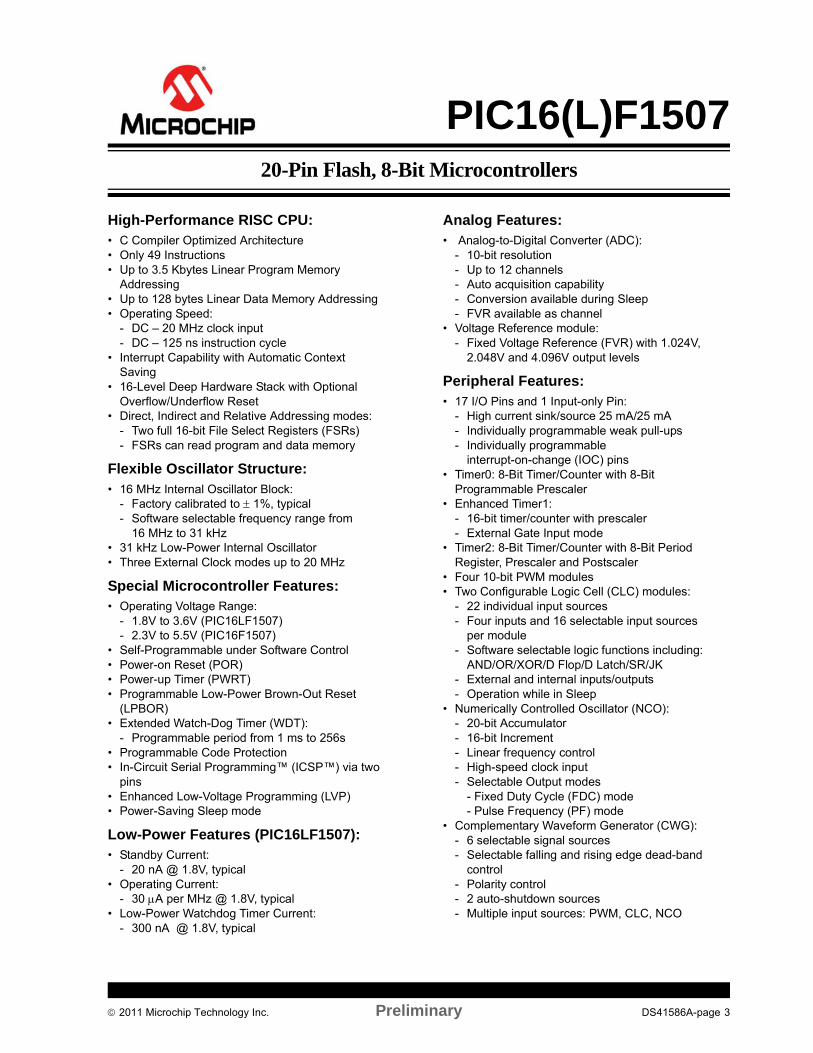
20-Pin Flash, 8-Bit Microcontrollers
PIC16(L)F1507
High-Performance RISC CPU:• C Compiler Optimized Architecture• Only 49 Instructions• Up to 3.5 Kbytes Linear Program Memory
Addressing• Up to 128 bytes Linear Data Memory Addressing• Operating Speed:
- DC – 20 MHz clock input- DC – 125 ns instruction cycle
• Interrupt Capability with Automatic Context Saving
• 16-Level Deep Hardware Stack with Optional Overflow/Underflow Reset
• Direct, Indirect and Relative Addressing modes:- Two full 16-bit File Select Registers (FSRs)- FSRs can read program and data memory
Flexible Oscillator Structure:• 16 MHz Internal Oscillator Block:
- Factory calibrated to 1%, typical- Software selectable frequency range from
16 MHz to 31 kHz• 31 kHz Low-Power Internal Oscillator • Three External Clock modes up to 20 MHz
Special Microcontroller Features:• Operating Voltage Range:
- 1.8V to 3.6V (PIC16LF1507)- 2.3V to 5.5V (PIC16F1507)
• Self-Programmable under Software Control• Power-on Reset (POR)• Power-up Timer (PWRT)• Programmable Low-Power Brown-Out Reset
(LPBOR)• Extended Watch-Dog Timer (WDT):
- Programmable period from 1 ms to 256s• Programmable Code Protection• In-Circuit Serial Programming™ (ICSP™) via two
pins• Enhanced Low-Voltage Programming (LVP)• Power-Saving Sleep mode
Low-Power Features (PIC16LF1507):• Standby Current:
- 20 nA @ 1.8V, typical • Operating Current:
- 30 A per MHz @ 1.8V, typical• Low-Power Watchdog Timer Current:
- 300 nA @ 1.8V, typical
Analog Features:• Analog-to-Digital Converter (ADC):
- 10-bit resolution- Up to 12 channels- Auto acquisition capability- Conversion available during Sleep- FVR available as channel
• Voltage Reference module:- Fixed Voltage Reference (FVR) with 1.024V,
2.048V and 4.096V output levels
Peripheral Features:• 17 I/O Pins and 1 Input-only Pin:
- High current sink/source 25 mA/25 mA- Individually programmable weak pull-ups- Individually programmable
interrupt-on-change (IOC) pins• Timer0: 8-Bit Timer/Counter with 8-Bit
Programmable Prescaler• Enhanced Timer1:
- 16-bit timer/counter with prescaler- External Gate Input mode
• Timer2: 8-Bit Timer/Counter with 8-Bit Period Register, Prescaler and Postscaler
• Four 10-bit PWM modules• Two Configurable Logic Cell (CLC) modules:
- 22 individual input sources- Four inputs and 16 selectable input sources
per module- Software selectable logic functions including:
AND/OR/XOR/D Flop/D Latch/SR/JK- External and internal inputs/outputs- Operation while in Sleep
• Numerically Controlled Oscillator (NCO):- 20-bit Accumulator- 16-bit Increment- Linear frequency control- High-speed clock input- Selectable Output modes
- Fixed Duty Cycle (FDC) mode- Pulse Frequency (PF) mode
• Complementary Waveform Generator (CWG):- 6 selectable signal sources- Selectable falling and rising edge dead-band
control- Polarity control- 2 auto-shutdown sources- Multiple input sources: PWM, CLC, NCO
2011 Microchip Technology Inc. Preliminary DS41586A-page 3
PIC16(L)F1507
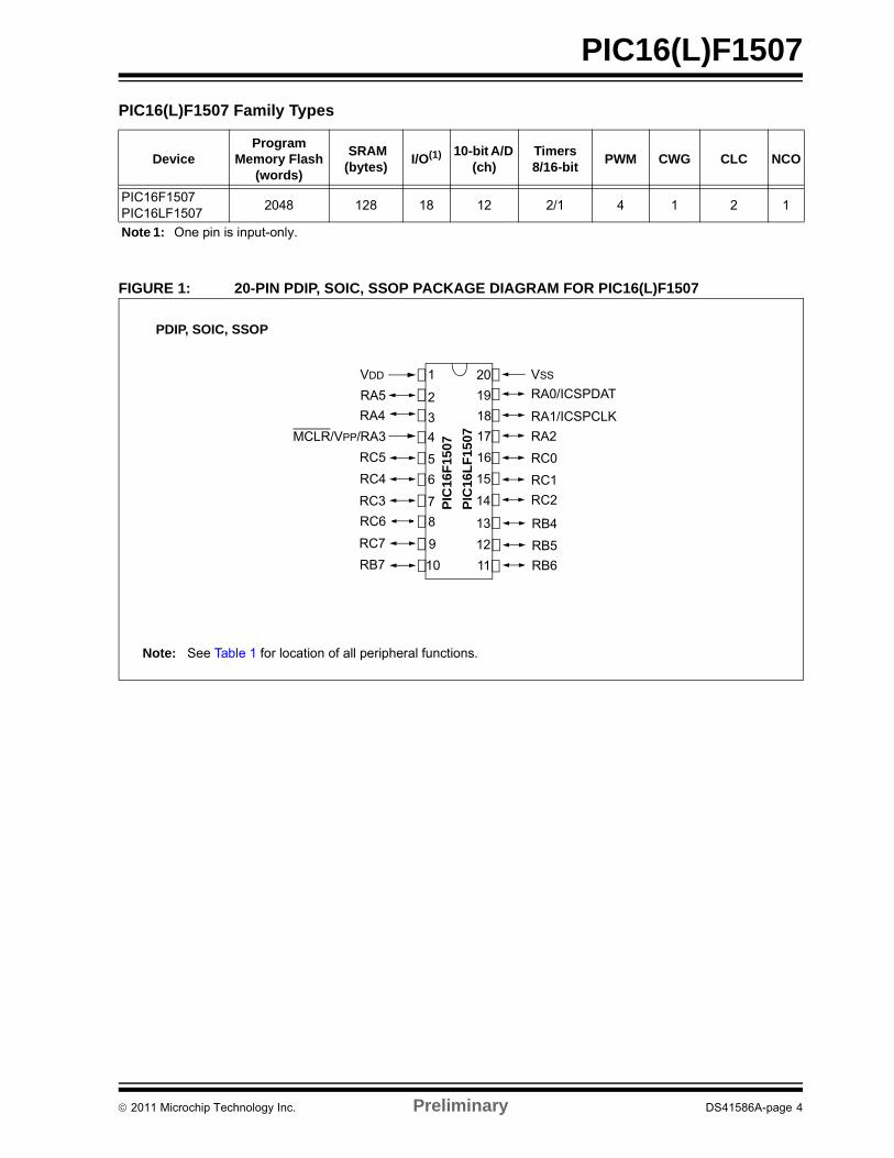
PIC16(L)F1507 Family Types
FIGURE 1: 20-PIN PDIP, SOIC, SSOP PACKAGE DIAGRAM FOR PIC16(L)F1507
DeviceProgram
Memory Flash(words)
SRAM (bytes)
I/O(1) 10-bit A/D (ch)
Timers8/16-bit
PWM CWG CLC NCO
PIC16F1507PIC16LF1507
2048 128 18 12 2/1 4 1 2 1
Note 1: One pin is input-only.
PIC
16F
1507
PIC
16L
F1
507
1
2
3
4
14
13
12
11
5
6
7
10
9
8
VDD
RA5
RA4
MCLR/VPP/RA3
RC5
RC4
VSS
RA0/ICSPDAT
RA1/ICSPCLK
RA2
RC0
RC1
RC2RC3
PDIP, SOIC, SSOP
Note: See Table 1 for location of all peripheral functions.
18
17
16
15
20
19
RC6
RC7
RB7
RB4
RB5
RB6
2011 Microchip Technology Inc. Preliminary DS41586A-page 4
PIC16(L)F1507
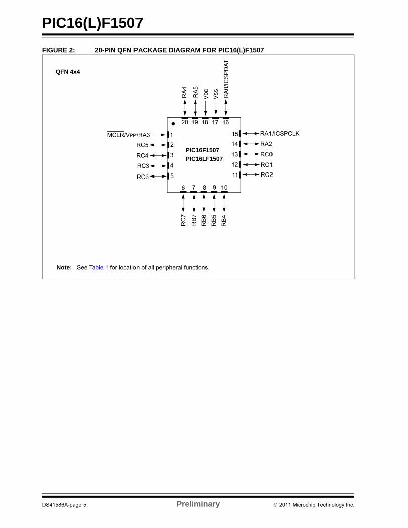
FIGURE 2: 20-PIN QFN PACKAGE DIAGRAM FOR PIC16(L)F1507
PIC16F1507
PIC16LF1507
QFN 4x4
Note: See Table 1 for location of all peripheral functions.
15 RA1/ICSPCLK
RA2
RC0
RC1
RC211
12
13
14
6 7R
C7
RB
7
RB
4
RB
5
RB
6
8 9 10
2
3
1
181920 1617
5
4
VD
D
RA
5
RA
4
MCLR/VPP/RA3
RC5
RC4
RC3
RC6
VS
S
RA
0/IC
SP
DA
T
DS41586A-page 5 Preliminary 2011 Microchip Technology Inc.
PIC16(L)F1507
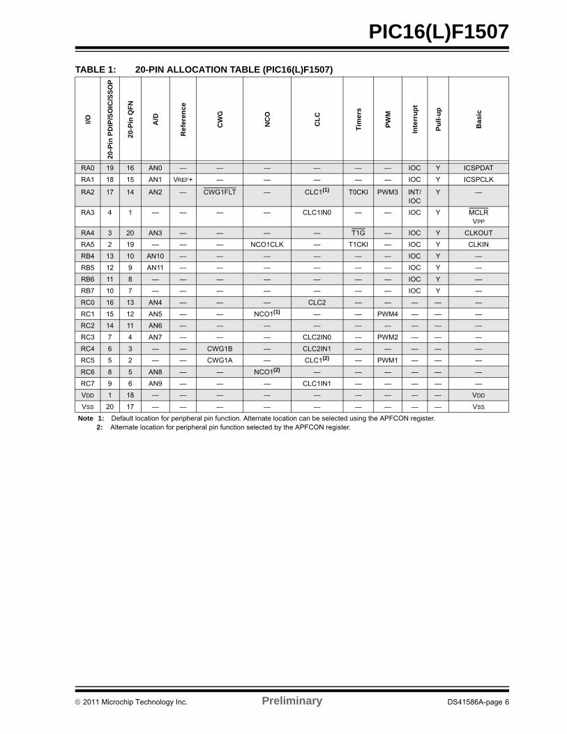
TABLE 1: 20-PIN ALLOCATION TABLE (PIC16(L)F1507)
I/O
20
-Pin
PD
IP/S
OIC
/SS
OP
20-
Pin
QF
N
A/D
Re
fere
nce
CW
G
NC
O
CL
C
Tim
ers
PW
M
Inte
rru
pt
Pu
ll-u
p
Ba
sic
RA0 19 16 AN0 — — — — — — IOC Y ICSPDAT
RA1 18 15 AN1 VREF+ — — — — — IOC Y ICSPCLK
RA2 17 14 AN2 — CWG1FLT — CLC1(1) T0CKI PWM3 INT/IOC
Y —
RA3 4 1 — — — — CLC1IN0 — — IOC Y MCLRVPP
RA4 3 20 AN3 — — — — T1G — IOC Y CLKOUT
RA5 2 19 — — — NCO1CLK — T1CKI — IOC Y CLKIN
RB4 13 10 AN10 — — — — — — IOC Y —
RB5 12 9 AN11 — — — — — — IOC Y —
RB6 11 8 — — — — — — — IOC Y —
RB7 10 7 — — — — — — — IOC Y —
RC0 16 13 AN4 — — — CLC2 — — — — —
RC1 15 12 AN5 — — NCO1(1) — — PWM4 — — —
RC2 14 11 AN6 — — — — — — — — —
RC3 7 4 AN7 — — — CLC2IN0 — PWM2 — — —
RC4 6 3 — — CWG1B — CLC2IN1 — — — — —
RC5 5 2 — — CWG1A — CLC1(2) — PWM1 — — —
RC6 8 5 AN8 — — NCO1(2) — — — — — —
RC7 9 6 AN9 — — — CLC1IN1 — — — — —
VDD 1 18 — — — — — — — — — VDD
VSS 20 17 — — — — — — — — — VSS
Note 1: Default location for peripheral pin function. Alternate location can be selected using the APFCON register.2: Alternate location for peripheral pin function selected by the APFCON register.
2011 Microchip Technology Inc. Preliminary DS41586A-page 6
PIC16(L)F1507
Table of Contents
1.0 Device Overview ............................................................................................................................................................................. 92.0.Enhanced Mid-Range CPU........................................................................................................................................................... 133.0 Memory Organization.................................................................................................................................................................... 154.0 Device Configuration..................................................................................................................................................................... 395.0 Oscillator Module (With Fail-Safe Clock Monitor) ......................................................................................................................... 456.0 Resets ........................................................................................................................................................................................... 537.0 Interrupts ....................................................................................................................................................................................... 618.0 Power-Down Mode (Sleep) ........................................................................................................................................................... 759.0 Watchdog Timer............................................................................................................................................................................ 7910.0 Flash Program Memory Control .................................................................................................................................................. 8311.0 I/O Ports ...................................................................................................................................................................................... 9912.0 Interrupt-On-Change ................................................................................................................................................................. 11113.0 Fixed Voltage Reference (FVR) ................................................................................................................................................ 11714.0 Temperature Indicator Module .................................................................................................................................................. 11915.0 Analog-to-Digital Converter (ADC) Module ............................................................................................................................... 12116.0 Timer0 Module .......................................................................................................................................................................... 13517.0 Timer1 Module with Gate Control ............................................................................................................................................. 13918.0 Timer2 Modules ........................................................................................................................................................................ 15119.0 PWM Modules ........................................................................................................................................................................... 15520.0 Configurable Logic Cell (CLC) ................................................................................................................................................... 16121.0 Numerically Controlled Oscillator (NCO) Module ...................................................................................................................... 17722.0 Complementary Waveform Generator (CWG) Module ............................................................................................................. 18723.0 In-Circuit Serial Programming™ (ICSP™) ................................................................................................................................ 20324.0 Instruction Set Summary ........................................................................................................................................................... 20725.0 Electrical Specifications ............................................................................................................................................................ 22126.0 DC and AC Characteristics Graphs and Charts ........................................................................................................................ 23927.0 Development Support ............................................................................................................................................................... 24128.0 Packaging Information .............................................................................................................................................................. 245Appendix A: Data Sheet Revision History ......................................................................................................................................... 255Index ................................................................................................................................................................................................. 257The Microchip Web Site .................................................................................................................................................................... 263Customer Change Notification Service ............................................................................................................................................. 263Customer Support ............................................................................................................................................................................. 263Reader Response ............................................................................................................................................................................. 264Product Identification System ............................................................................................................................................................ 265Worldwide Sales and Service ........................................................................................................................................................... 266
DS41586A-page 7 Preliminary 2011 Microchip Technology Inc.

PIC16(L)F1507
NOTES:
2011 Microchip Technology Inc. Preliminary DS41586A-page 8
PIC16(L)F1507
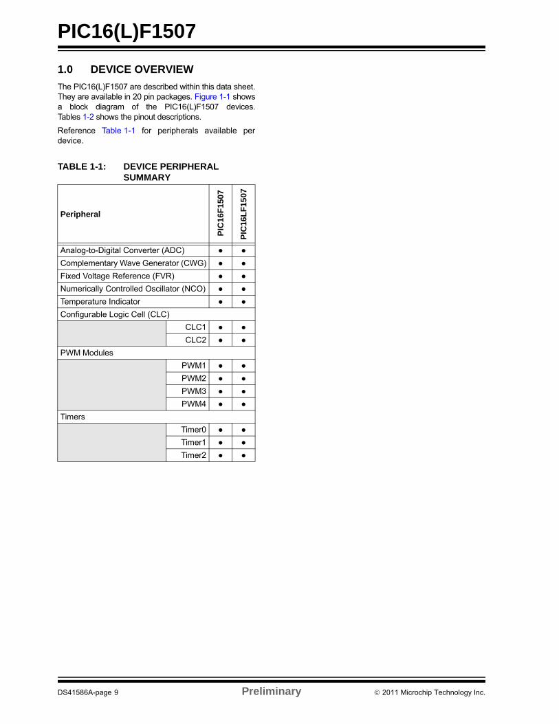
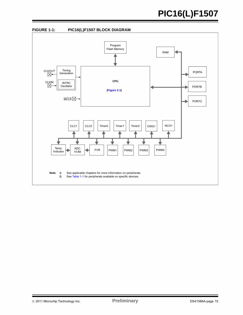
1.0 DEVICE OVERVIEW
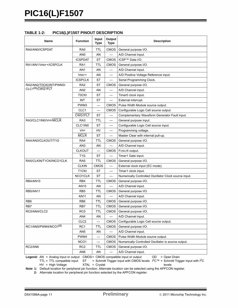
The PIC16(L)F1507 are described within this data sheet.They are available in 20 pin packages. Figure 1-1 showsa block diagram of the PIC16(L)F1507 devices.Tables 1-2 shows the pinout descriptions.
Reference Table 1-1 for peripherals available perdevice.
TABLE 1-1: DEVICE PERIPHERAL SUMMARY
Peripheral P
IC1
6F1
507
PIC
16L
F1
507
Analog-to-Digital Converter (ADC) ● ●
Complementary Wave Generator (CWG) ● ●
Fixed Voltage Reference (FVR) ● ●
Numerically Controlled Oscillator (NCO) ● ●
Temperature Indicator ● ●
Configurable Logic Cell (CLC)
CLC1 ● ●
CLC2 ● ●
PWM Modules
PWM1 ● ●
PWM2 ● ●
PWM3 ● ●
PWM4 ● ●
Timers
Timer0 ● ●
Timer1 ● ●
Timer2 ● ●
DS41586A-page 9 Preliminary 2011 Microchip Technology Inc.
PIC16(L)F1507
FIGURE 1-1: PIC16(L)F1507 BLOCK DIAGRAM
PORTB
PORTC
Note 1: See applicable chapters for more information on peripherals.2: See Table 1-1 for peripherals available on specific devices.
CPU
ProgramFlash Memory
RAM
TimingGeneration
INTRCOscillator
MCLR
(Figure 2-1)
NCO1
PWM4
Timer2Timer1Timer0CLC2
PWM1 PWM2 PWM3
PORTA
CWG1CLC1
ADC10-Bit
FVRTemp.
Indicator
CLKIN
CLKOUT
2011 Microchip Technology Inc. Preliminary DS41586A-page 10
PIC16(L)F1507
TABLE 1-2: PIC16(L)F1507 PINOUT DESCRIPTION
Name FunctionInput Type
Output Type
Description
RA0/AN0/ICSPDAT RA0 TTL CMOS General purpose I/O.
AN0 AN — A/D Channel input.
ICSPDAT ST CMOS ICSP™ Data I/O.
RA1/AN1/VREF+/ICSPCLK RA1 TTL CMOS General purpose I/O.
AN1 AN — A/D Channel input.
VREF+ AN — A/D Positive Voltage Reference input.
ICSPCLK ST — Serial Programming Clock.
RA2/AN2/T0CKI/INT/PWM3/CLC1(1)/CWG1FLT
RA2 ST CMOS General purpose I/O.
AN2 AN — A/D Channel input.
T0CKI ST — Timer0 clock input.
INT ST — External interrupt.
PWM3 — CMOS Pulse Width Module source output.
CLC1 — CMOS Configurable Logic Cell source output.
CWG1FLT ST — Complementary Waveform Generator Fault input.
RA3/CLC1IN0/VPP/MCLR RA3 TTL — General purpose input.
CLC1IN0 ST — Configurable Logic Cell source input.
VPP HV — Programming voltage.
MCLR ST — Master Clear with internal pull-up.
RA4/AN3/CLKOUT/T1G RA4 TTL CMOS General purpose I/O.
AN3 AN — A/D Channel input.
CLKOUT — CMOS FOSC/4 output.
T1G ST — Timer1 Gate input.
RA5/CLKIN/T1CKI/NCO1CLK RA5 TTL CMOS General purpose I/O.
CLKIN CMOS — External clock input (EC mode).
T1CKI ST — Timer1 clock input.
NCO1CLK ST — Numerically Controlled Oscillator Clock source input.
RB4/AN10 RB4 TTL CMOS General purpose I/O.
AN10 AN — A/D Channel input.
RB5/AN11 RB5 TTL CMOS General purpose I/O.
AN11 AN — A/D Channel input.
RB6 RB6 TTL CMOS General purpose I/O.
RB7 RB7 TTL CMOS General purpose I/O.
RC0/AN4/CLC2 RC0 TTL CMOS General purpose I/O.
AN4 AN — A/D Channel input.
CLC2 — CMOS Configurable Logic Cell source output.
RC1/AN5/PWM4/NCO1(1) RC1 TTL CMOS General purpose I/O.
AN5 AN — A/D Channel input.
PWM4 — CMOS Pulse Width Module source output.
NCO1 — CMOS Numerically Controlled Oscillator is source output.
RC2/AN6 RC2 TTL CMOS General purpose I/O.
AN6 AN — A/D Channel input.
Legend: AN = Analog input or output CMOS= CMOS compatible input or output OD = Open DrainTTL = TTL compatible input ST = Schmitt Trigger input with CMOS levels I2C™ = Schmitt Trigger input with I2C HV = High Voltage XTAL = Crystal levels
Note 1: Default location for peripheral pin function. Alternate location can be selected using the APFCON register.2: Alternate location for peripheral pin function selected by the APFCON register.
DS41586A-page 11 Preliminary 2011 Microchip Technology Inc.
PIC16(L)F1507
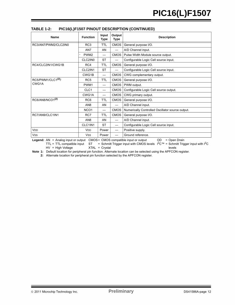
RC3/AN7/PWM2/CLC2IN0 RC3 TTL CMOS General purpose I/O.
AN7 AN — A/D Channel input.
PWM2 — CMOS Pulse Width Module source output.
CLC2IN0 ST — Configurable Logic Cell source input.
RC4/CLC2IN1/CWG1B RC4 TTL CMOS General purpose I/O.
CLC2IN1 ST — Configurable Logic Cell source input.
CWG1B — CMOS CWG complementary output.
RC5/PWM1/CLC1(2)/CWG1A
RC5 TTL CMOS General purpose I/O.
PWM1 — CMOS PWM output.
CLC1 — CMOS Configurable Logic Cell source output.
CWG1A — CMOS CWG primary output.
RC6/AN8/NCO1(2) RC6 TTL CMOS General purpose I/O.
AN8 AN — A/D Channel input.
NCO1 — CMOS Numerically Controlled Oscillator source output.
RC7/AN9/CLC1IN1 RC7 TTL CMOS General purpose I/O.
AN8 AN — A/D Channel input.
CLC1IN1 ST — Configurable Logic Cell source input.
VDD VDD Power — Positive supply.
VSS VSS Power — Ground reference.
TABLE 1-2: PIC16(L)F1507 PINOUT DESCRIPTION (CONTINUED)
Name FunctionInput Type
Output Type
Description
Legend: AN = Analog input or output CMOS= CMOS compatible input or output OD = Open DrainTTL = TTL compatible input ST = Schmitt Trigger input with CMOS levels I2C™ = Schmitt Trigger input with I2C HV = High Voltage XTAL = Crystal levels
Note 1: Default location for peripheral pin function. Alternate location can be selected using the APFCON register.2: Alternate location for peripheral pin function selected by the APFCON register.
2011 Microchip Technology Inc. Preliminary DS41586A-page 12
PIC16(L)F1507
2.0 ENHANCED MID-RANGE CPU
This family of devices contain an enhanced mid-range8-bit CPU core. The CPU has 49 instructions. Interruptcapability includes automatic context saving. Thehardware stack is 16 levels deep and has Overflow andUnderflow Reset capability. Direct, Indirect, andRelative addressing modes are available. Two FileSelect Registers (FSRs) provide the ability to readprogram and data memory.
• Automatic Interrupt Context Saving
• 16-level Stack with Overflow and Underflow
• File Select Registers
• Instruction Set
2.1 Automatic Interrupt Context Saving
During interrupts, certain registers are automaticallysaved in shadow registers and restored when returningfrom the interrupt. This saves stack space and usercode. See Section 7.5 “Automatic Context Saving”,for more information.
2.2 16-level Stack with Overflow and Underflow
These devices have an external stack memory 15 bitswide and 16 words deep. A Stack Overflow or Under-flow will set the appropriate bit (STKOVF or STKUNF)in the PCON register, and if enabled will cause a soft-ware Reset. See section Section 3.4 “Stack” for moredetails.
2.3 File Select Registers
There are two 16-bit File Select Registers (FSR). FSRscan access all file registers and program memory,which allows one Data Pointer for all memory. When anFSR points to program memory, there is one additionalinstruction cycle in instructions using INDF to allow thedata to be fetched. General purpose memory can nowalso be addressed linearly, providing the ability toaccess contiguous data larger than 80 bytes. There arealso new instructions to support the FSRs. SeeSection 3.5 “Indirect Addressing” for more details.
2.4 Instruction Set
There are 49 instructions for the enhanced mid-rangeCPU to support the features of the CPU. SeeSection 24.0 “Instruction Set Summary” for moredetails.
DS41586A-page 13 Preliminary 2011 Microchip Technology Inc.
PIC16(L)F1507
FIGURE 2-1: CORE BLOCK DIAGRAM
Data Bus 8
14ProgramBus
Instruction reg
Program Counter
8 Level Stack(13-bit)
Direct Addr 7
12
Addr MUX
FSR reg
STATUS reg
MUX
ALU
InstructionDecode &
Control
TimingGeneration
CLKIN
CLKOUT
8
8
12
3
InternalOscillator
Block
ConfigurationData Bus 8
14ProgramBus
Instruction reg
Program Counter
8 Level Stack(13-bit)
Direct Addr 7
Addr MUX
FSR reg
STATUS reg
MUX
ALU
W Reg
InstructionDecode &
Control
TimingGeneration
8
8
3
InternalOscillator
Block
Configuration 15 Data Bus 8
14ProgramBus
Instruction Reg
Program Counter
16-Level Stack(15-bit)
Direct Addr 7
RAM Addr
Addr MUX
IndirectAddr
FSR0 Reg
STATUS Reg
MUX
ALU
InstructionDecode and
Control
TimingGeneration
8
8
3
InternalOscillator
Block
Configuration
Flash
ProgramMemory
RAM
FSR regFSR regFSR1 Reg
15
15
MU
X
15
Program Memory
Read (PMR)
12
FSR regFSR regBSR Reg
5
Power-upTimer
Power-onReset
WatchdogTimer
VDD
Brown-outReset
VSSVDD VSSVDD VSS
2011 Microchip Technology Inc. Preliminary DS41586A-page 14
PIC16(L)F1507
3.0 MEMORY ORGANIZATION
These devices contain the following types of memory:
• Program Memory
- Configuration Words
- Device ID
- User ID
- Flash Program Memory
• Data Memory
- Core Registers
- Special Function Registers
- General Purpose RAM
- Common RAM
The following features are associated with access andcontrol of program memory and data memory:
• PCL and PCLATH
• Stack
• Indirect Addressing
3.1 Program Memory Organization
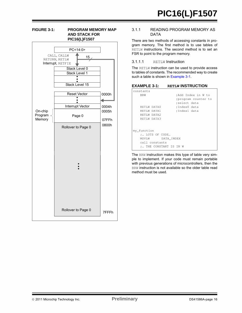
The enhanced mid-range core has a 15-bit programcounter capable of addressing 32K x 14 programmemory space. Table 3-1 shows the memory sizesimplemented. Accessing a location above theseboundaries will cause a wrap-around within theimplemented memory space. The Reset vector is at0000h and the interrupt vector is at 0004h (SeeFigure 3-1).
TABLE 3-1: DEVICE SIZES AND ADDRESSES
Device Program Memory Space (Words) Last Program Memory Address
PIC16F1507PIC16LF1507
2,048 07FFh
DS41586A-page 15 Preliminary 2011 Microchip Technology Inc.
PIC16(L)F1507
FIGURE 3-1: PROGRAM MEMORY MAP AND STACK FOR PIC16(L)F1507
3.1.1 READING PROGRAM MEMORY AS DATA
There are two methods of accessing constants in pro-gram memory. The first method is to use tables ofRETLW instructions. The second method is to set anFSR to point to the program memory.
3.1.1.1 RETLW Instruction
The RETLW instruction can be used to provide accessto tables of constants. The recommended way to createsuch a table is shown in Example 3-1.
EXAMPLE 3-1: RETLW INSTRUCTION
The BRW instruction makes this type of table very sim-ple to implement. If your code must remain portablewith previous generations of microcontrollers, then theBRW instruction is not available so the older table readmethod must be used.
PC<14:0>
15
0000h
0004h
Stack Level 0
Stack Level 15
Reset Vector
Interrupt Vector
Stack Level 1
0005hOn-chipProgramMemory
Page 007FFh
Wraps to Page 0
Wraps to Page 0
Wraps to Page 0
0800h
CALL, CALLW RETURN, RETLW
Interrupt, RETFIE
Rollover to Page 0
Rollover to Page 07FFFh
constantsBRW ;Add Index in W to
;program counter to;select data
RETLW DATA0 ;Index0 dataRETLW DATA1 ;Index1 dataRETLW DATA2RETLW DATA3
my_function;… LOTS OF CODE…MOVLW DATA_INDEXcall constants;… THE CONSTANT IS IN W
2011 Microchip Technology Inc. Preliminary DS41586A-page 16
PIC16(L)F1507
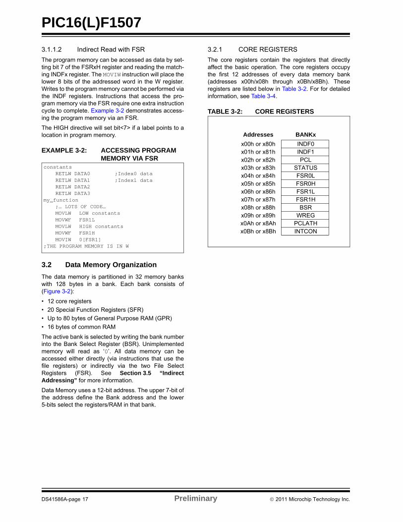
3.1.1.2 Indirect Read with FSR
The program memory can be accessed as data by set-ting bit 7 of the FSRxH register and reading the match-ing INDFx register. The MOVIW instruction will place thelower 8 bits of the addressed word in the W register.Writes to the program memory cannot be performed viathe INDF registers. Instructions that access the pro-gram memory via the FSR require one extra instructioncycle to complete. Example 3-2 demonstrates access-ing the program memory via an FSR.
The HIGH directive will set bit<7> if a label points to alocation in program memory.
EXAMPLE 3-2: ACCESSING PROGRAM MEMORY VIA FSR
3.2 Data Memory Organization
The data memory is partitioned in 32 memory bankswith 128 bytes in a bank. Each bank consists of(Figure 3-2):
• 12 core registers
• 20 Special Function Registers (SFR)
• Up to 80 bytes of General Purpose RAM (GPR)
• 16 bytes of common RAM
The active bank is selected by writing the bank numberinto the Bank Select Register (BSR). Unimplementedmemory will read as ‘0’. All data memory can beaccessed either directly (via instructions that use thefile registers) or indirectly via the two File SelectRegisters (FSR). See Section 3.5 “IndirectAddressing” for more information.
Data Memory uses a 12-bit address. The upper 7-bit ofthe address define the Bank address and the lower5-bits select the registers/RAM in that bank.
3.2.1 CORE REGISTERS
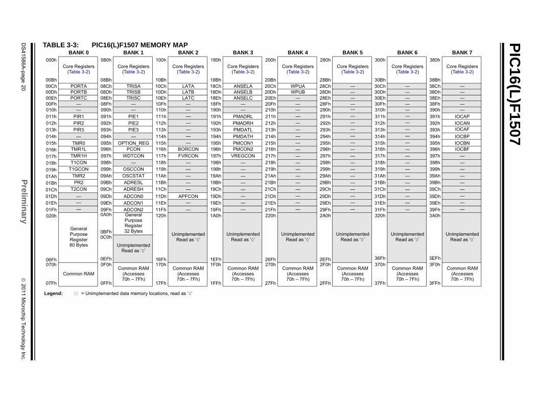
The core registers contain the registers that directlyaffect the basic operation. The core registers occupythe first 12 addresses of every data memory bank(addresses x00h/x08h through x0Bh/x8Bh). Theseregisters are listed below in Table 3-2. For for detailedinformation, see Table 3-4.
TABLE 3-2: CORE REGISTERS
constantsRETLW DATA0 ;Index0 dataRETLW DATA1 ;Index1 dataRETLW DATA2RETLW DATA3
my_function;… LOTS OF CODE…MOVLW LOW constantsMOVWF FSR1LMOVLW HIGH constantsMOVWF FSR1HMOVIW 0[FSR1]
;THE PROGRAM MEMORY IS IN W
Addresses BANKx
x00h or x80h INDF0x01h or x81h INDF1x02h or x82h PCLx03h or x83h STATUSx04h or x84h FSR0Lx05h or x85h FSR0Hx06h or x86h FSR1Lx07h or x87h FSR1Hx08h or x88h BSRx09h or x89h WREGx0Ah or x8Ah PCLATHx0Bh or x8Bh INTCON
DS41586A-page 17 Preliminary 2011 Microchip Technology Inc.
PIC16(L)F1507
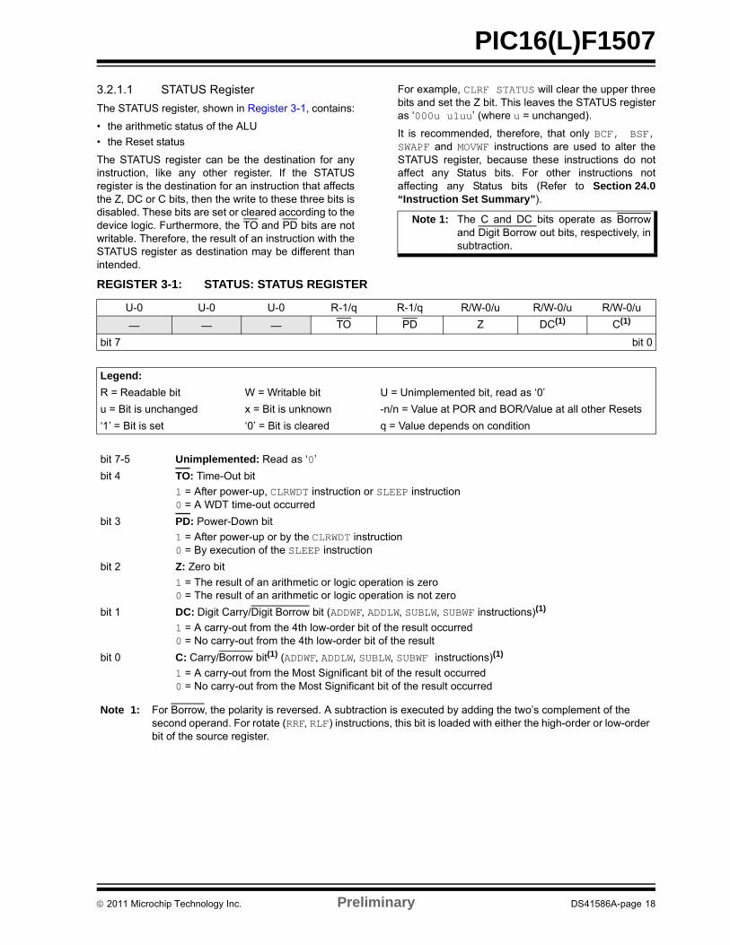
3.2.1.1 STATUS Register
The STATUS register, shown in Register 3-1, contains:
• the arithmetic status of the ALU
• the Reset status
The STATUS register can be the destination for anyinstruction, like any other register. If the STATUSregister is the destination for an instruction that affectsthe Z, DC or C bits, then the write to these three bits isdisabled. These bits are set or cleared according to thedevice logic. Furthermore, the TO and PD bits are notwritable. Therefore, the result of an instruction with theSTATUS register as destination may be different thanintended.
For example, CLRF STATUS will clear the upper threebits and set the Z bit. This leaves the STATUS registeras ‘000u u1uu’ (where u = unchanged).
It is recommended, therefore, that only BCF, BSF,SWAPF and MOVWF instructions are used to alter theSTATUS register, because these instructions do notaffect any Status bits. For other instructions notaffecting any Status bits (Refer to Section 24.0“Instruction Set Summary”).
Note 1: The C and DC bits operate as Borrowand Digit Borrow out bits, respectively, insubtraction.
REGISTER 3-1: STATUS: STATUS REGISTER
U-0 U-0 U-0 R-1/q R-1/q R/W-0/u R/W-0/u R/W-0/u
— — — TO PD Z DC(1) C(1)
bit 7 bit 0
Legend:
R = Readable bit W = Writable bit U = Unimplemented bit, read as ‘0’
u = Bit is unchanged x = Bit is unknown -n/n = Value at POR and BOR/Value at all other Resets
‘1’ = Bit is set ‘0’ = Bit is cleared q = Value depends on condition
bit 7-5 Unimplemented: Read as ‘0’
bit 4 TO: Time-Out bit
1 = After power-up, CLRWDT instruction or SLEEP instruction0 = A WDT time-out occurred
bit 3 PD: Power-Down bit
1 = After power-up or by the CLRWDT instruction0 = By execution of the SLEEP instruction
bit 2 Z: Zero bit
1 = The result of an arithmetic or logic operation is zero0 = The result of an arithmetic or logic operation is not zero
bit 1 DC: Digit Carry/Digit Borrow bit (ADDWF, ADDLW, SUBLW, SUBWF instructions)(1)
1 = A carry-out from the 4th low-order bit of the result occurred0 = No carry-out from the 4th low-order bit of the result
bit 0 C: Carry/Borrow bit(1) (ADDWF, ADDLW, SUBLW, SUBWF instructions)(1)
1 = A carry-out from the Most Significant bit of the result occurred0 = No carry-out from the Most Significant bit of the result occurred
Note 1: For Borrow, the polarity is reversed. A subtraction is executed by adding the two’s complement of the second operand. For rotate (RRF, RLF) instructions, this bit is loaded with either the high-order or low-order bit of the source register.
2011 Microchip Technology Inc. Preliminary DS41586A-page 18
PIC16(L)F1507
3.2.2 SPECIAL FUNCTION REGISTER
The Special Function Registers are registers used bythe application to control the desired operation ofperipheral functions in the device. The Special FunctionRegisters occupy the 20 bytes after the core registers ofevery data memory bank (addresses x0Ch/x8Chthrough x1Fh/x9Fh). The registers associated with theoperation of the peripherals are described in the appro-priate peripheral chapter of this data sheet.
3.2.3 GENERAL PURPOSE RAM
There are up to 80 bytes of GPR in each data memorybank. The Special Function Registers occupy the 20bytes after the core registers of every data memorybank (addresses x0Ch/x8Ch through x1Fh/x9Fh).
3.2.3.1 Linear Access to GPR
The general purpose RAM can be accessed in anon-banked method via the FSRs. This can simplifyaccess to large memory structures. See Section 3.5.2“Linear Data Memory” for more information.
3.2.4 COMMON RAM
There are 16 bytes of common RAM accessible from allbanks.
FIGURE 3-2: BANKED MEMORY PARTITIONING
3.2.5 DEVICE MEMORY MAPS
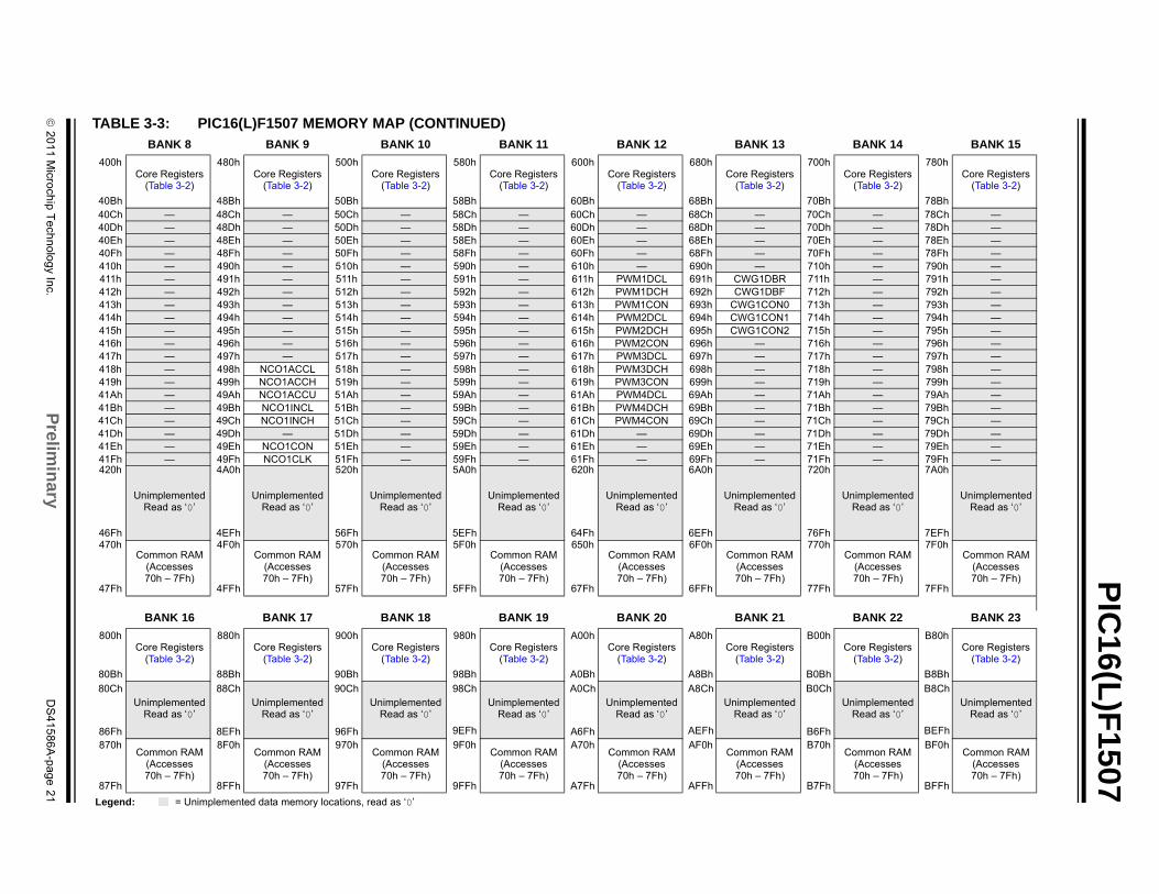
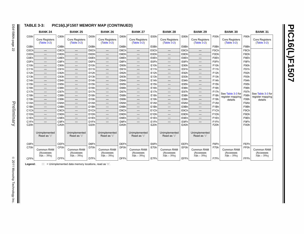
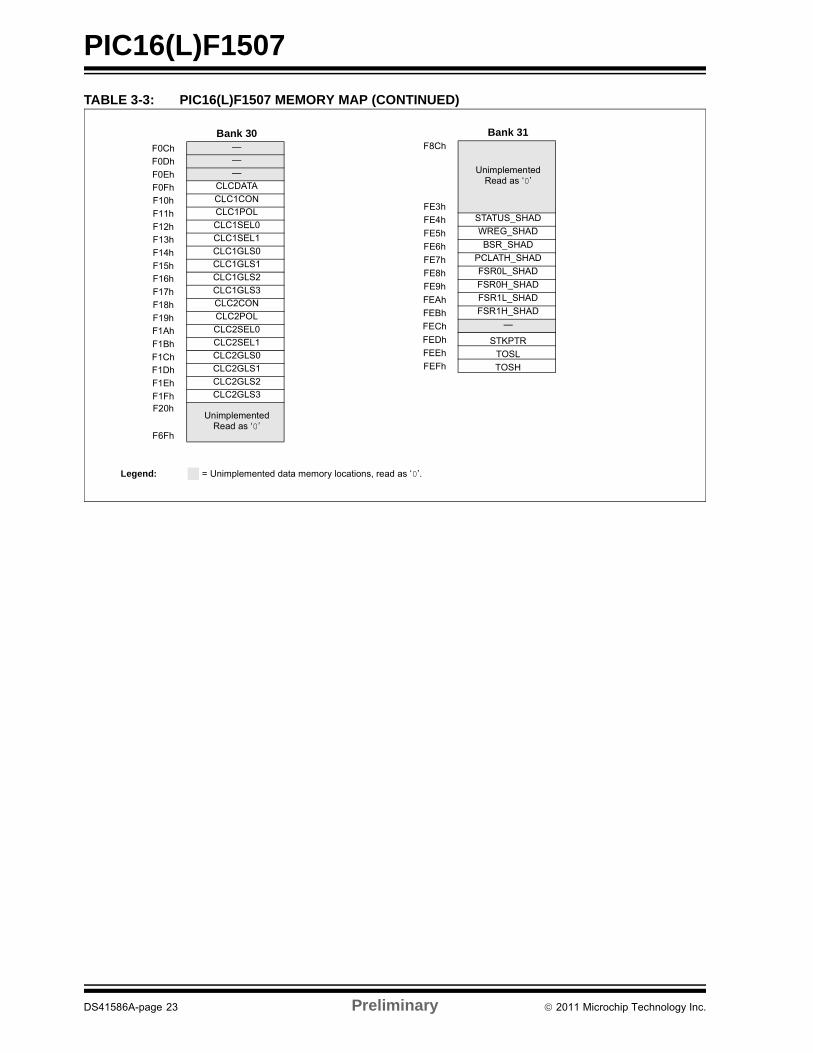
The memory maps for PIC16(L)F1507 are as shown inTable 3-3.
0Bh0Ch
1Fh
20h
6Fh70h
7Fh
00h
Common RAM(16 bytes)
General Purpose RAM(80 bytes maximum)
Core Registers(12 bytes)
Special Function Registers(20 bytes maximum)
Memory Region7-bit Bank Offset
DS41586A-page 19 Preliminary 2011 Microchip Technology Inc.
PIC
16(L)F
1507
DS
41
58
6A
-pa
ge
20
Prelim
inary
2
01
1 M
icroch
ip T
ech
no
log
y Inc.
BANK 6 BANK 7
300h
Core Registers (Table 3-2)
380hCore Registers
(Table 3-2)
30Bh 38Bh30Ch — 38Ch —30Dh — 38Dh —30Eh — 38Eh —30Fh — 38Fh —310h — 390h —
311h — 391h IOCAP
312h — 392h IOCAN
313h — 393h IOCAF
314h — 394h IOCBP
315h — 395h IOCBN316h — 396h IOCBF
317h — 397h —
318h — 398h —
319h — 399h —
31Ah — 39Ah —
31Bh — 39Bh —
31Ch — 39Ch —
31Dh — 39Dh —
31Eh — 39Eh —
31Fh — 39Fh —320h
UnimplementedRead as ‘0’
3A0h
UnimplementedRead as ‘0’
36Fh 3EFh370h
Common RAM(Accesses70h – 7Fh)
3F0hCommon RAM
(Accesses70h – 7Fh)
37Fh 3FFh
TABLE 3-3: PIC16(L)F1507 MEMORY MAPBANK 0 BANK 1 BANK 2 BANK 3 BANK 4 BANK 5
000hCore Registers
(Table 3-2)
080hCore Registers
(Table 3-2)
100hCore Registers
(Table 3-2)
180hCore Registers
(Table 3-2)
200hCore Registers
(Table 3-2)
280hCore Registers
(Table 3-2)
00Bh 08Bh 10Bh 18Bh 20Bh 28Bh00Ch PORTA 08Ch TRISA 10Ch LATA 18Ch ANSELA 20Ch WPUA 28Ch —00Dh PORTB 08Dh TRISB 10Dh LATB 18Dh ANSELB 20Dh WPUB 28Dh —00Eh PORTC 08Eh TRISC 10Eh LATC 18Eh ANSELC 20Eh — 28Eh —00Fh — 08Fh — 10Fh — 18Fh — 20Fh — 28Fh —010h — 090h — 110h — 190h — 210h — 290h —
011h PIR1 091h PIE1 111h — 191h PMADRL 211h — 291h —
012h PIR2 092h PIE2 112h — 192h PMADRH 212h — 292h —
013h PIR3 093h PIE3 113h — 193h PMDATL 213h — 293h —
014h — 094h — 114h — 194h PMDATH 214h — 294h —
015h TMR0 095h OPTION_REG 115h — 195h PMCON1 215h — 295h —
016h TMR1L 096h PCON 116h BORCON 196h PMCON2 216h — 296h —
017h TMR1H 097h WDTCON 117h FVRCON 197h VREGCON 217h — 297h —
018h T1CON 098h — 118h — 198h — 218h — 298h —
019h T1GCON 099h OSCCON 119h — 199h — 219h — 299h —
01Ah TMR2 09Ah OSCSTAT 11Ah — 19Ah — 21Ah — 29Ah —
01Bh PR2 09Bh ADRESL 11Bh — 19Bh — 21Bh — 29Bh —
01Ch T2CON 09Ch ADRESH 11Ch — 19Ch — 21Ch — 29Ch —
01Dh — 09Dh ADCON0 11Dh APFCON 19Dh — 21Dh — 29Dh —
01Eh — 09Eh ADCON1 11Eh — 19Eh — 21Eh — 29Eh —
01Fh — 09Fh ADCON2 11Fh — 19Fh — 21Fh — 29Fh —
020h
GeneralPurposeRegister80 Bytes
0A0h
0BFh
GeneralPurposeRegister32 Bytes
120h
UnimplementedRead as ‘0’
1A0h
UnimplementedRead as ‘0’
220h
UnimplementedRead as ‘0’
2A0h
UnimplementedRead as ‘0’0C0h
0EFh
UnimplementedRead as ‘0’
06Fh 16Fh 1EFh 26Fh 2EFh070h
Common RAM
0F0hCommon RAM
(Accesses70h – 7Fh)
170hCommon RAM
(Accesses70h – 7Fh)
1F0hCommon RAM
(Accesses70h – 7Fh)
270hCommon RAM
(Accesses70h – 7Fh)
2F0hCommon RAM
(Accesses70h – 7Fh)
07Fh 0FFh 17Fh 1FFh 27Fh 2FFh
Legend: = Unimplemented data memory locations, read as ‘0’
2
01
1 M
icroch
ip T
ech
no
log
y Inc.
Prelim
inary
DS
41
58
6A
-pa
ge
21
PIC
16(L)F
1507
TABANK 14 BANK 15
40
40
h
h
Core Registers (Table 3-2)
780h
78Bh
Core Registers (Table 3-2)
40 h — 78Ch —40 h — 78Dh —40 h — 78Eh —40 h — 78Fh —41 h — 790h —41 h — 791h —41 h — 792h —41 h — 793h —41 h — 794h —41 h — 795h —41 h — 796h —41 h — 797h —41 h — 798h —41 h — 799h —41 h — 79Ah —41 h — 79Bh —41 h — 79Ch —41 h — 79Dh —41 h — 79Eh —41 h — 79Fh —42 h
UnimplementedRead as ‘0’
7A0h
UnimplementedRead as ‘0’
46 h 7EFh47 h
Common RAM(Accesses70h – 7Fh)
7F0hCommon RAM
(Accesses70h – 7Fh)
47 h 7FFh
BANK 22 BANK 23
80
80
h
h
Core Registers (Table 3-2)
B80h
B8Bh
Core Registers (Table 3-2)
80 hUnimplemented
Read as ‘0’
B8ChUnimplemented
Read as ‘0’
86 h BEFh
87 hCommon RAM
(Accesses70h – 7Fh)
BF0hCommon RAM
(Accesses70h – 7Fh)
87 h BFFh
Le
BLE 3-3: PIC16(L)F1507 MEMORY MAP (CONTINUED)BANK 8 BANK 9 BANK 10 BANK 11 BANK 12 BANK 13
0h
Bh
Core Registers (Table 3-2)
480h
48Bh
Core Registers (Table 3-2)
500h
50Bh
Core Registers (Table 3-2)
580h
58Bh
Core Registers (Table 3-2)
600h
60Bh
Core Registers (Table 3-2)
680h
68Bh
Core Registers (Table 3-2)
700
70BCh — 48Ch — 50Ch — 58Ch — 60Ch — 68Ch — 70CDh — 48Dh — 50Dh — 58Dh — 60Dh — 68Dh — 70DEh — 48Eh — 50Eh — 58Eh — 60Eh — 68Eh — 70EFh — 48Fh — 50Fh — 58Fh — 60Fh — 68Fh — 70F0h — 490h — 510h — 590h — 610h — 690h — 7101h — 491h — 511h — 591h — 611h PWM1DCL 691h CWG1DBR 7112h — 492h — 512h — 592h — 612h PWM1DCH 692h CWG1DBF 7123h — 493h — 513h — 593h — 613h PWM1CON 693h CWG1CON0 7134h — 494h — 514h — 594h — 614h PWM2DCL 694h CWG1CON1 7145h — 495h — 515h — 595h — 615h PWM2DCH 695h CWG1CON2 7156h — 496h — 516h — 596h — 616h PWM2CON 696h — 7167h — 497h — 517h — 597h — 617h PWM3DCL 697h — 7178h — 498h NCO1ACCL 518h — 598h — 618h PWM3DCH 698h — 7189h — 499h NCO1ACCH 519h — 599h — 619h PWM3CON 699h — 719Ah — 49Ah NCO1ACCU 51Ah — 59Ah — 61Ah PWM4DCL 69Ah — 71ABh — 49Bh NCO1INCL 51Bh — 59Bh — 61Bh PWM4DCH 69Bh — 71BCh — 49Ch NCO1INCH 51Ch — 59Ch — 61Ch PWM4CON 69Ch — 71CDh — 49Dh — 51Dh — 59Dh — 61Dh — 69Dh — 71DEh — 49Eh NCO1CON 51Eh — 59Eh — 61Eh — 69Eh — 71EFh — 49Fh NCO1CLK 51Fh — 59Fh — 61Fh — 69Fh — 71F0h
UnimplementedRead as ‘0’
4A0h
UnimplementedRead as ‘0’
520h
UnimplementedRead as ‘0’
5A0h
UnimplementedRead as ‘0’
620h
UnimplementedRead as ‘0’
6A0h
UnimplementedRead as ‘0’
720
Fh 4EFh 56Fh 5EFh 64Fh 6EFh 76F0h
Common RAM(Accesses70h – 7Fh)
4F0hCommon RAM
(Accesses70h – 7Fh)
570hCommon RAM
(Accesses70h – 7Fh)
5F0hCommon RAM
(Accesses70h – 7Fh)
650hCommon RAM
(Accesses70h – 7Fh)
6F0hCommon RAM
(Accesses70h – 7Fh)
770
Fh 4FFh 57Fh 5FFh 67Fh 6FFh 77F
BANK 16 BANK 17 BANK 18 BANK 19 BANK 20 BANK 21
0h
Bh
Core Registers (Table 3-2)
880h
88Bh
Core Registers (Table 3-2)
900h
90Bh
Core Registers (Table 3-2)
980h
98Bh
Core Registers (Table 3-2)
A00h
A0Bh
Core Registers (Table 3-2)
A80h
A8Bh
Core Registers (Table 3-2)
B00
B0B
ChUnimplemented
Read as ‘0’
88ChUnimplemented
Read as ‘0’
90ChUnimplemented
Read as ‘0’
98ChUnimplemented
Read as ‘0’
A0ChUnimplemented
Read as ‘0’
A8ChUnimplemented
Read as ‘0’
B0C
Fh 8EFh 96Fh 9EFh A6Fh AEFh B6F0h
Common RAM(Accesses70h – 7Fh)
8F0hCommon RAM
(Accesses70h – 7Fh)
970hCommon RAM
(Accesses70h – 7Fh)
9F0hCommon RAM
(Accesses70h – 7Fh)
A70hCommon RAM
(Accesses70h – 7Fh)
AF0hCommon RAM
(Accesses70h – 7Fh)
B70
Fh 8FFh 97Fh 9FFh A7Fh AFFh B7F
gend: = Unimplemented data memory locations, read as ‘0’
PIC
16(L)F
1507
DS
41
58
6A
-pa
ge
22
Prelim
inary
2
01
1 M
icroch
ip T
ech
no
log
y Inc.
BANK 30 BANK 31
s F00h
F0Bh
Core Registers (Table 3-2)
F80h
F8Bh
Core Registers (Table 3-2)
F0Ch
See Table 3-3 for register mapping
details
F8Ch
See Table 3-3 for register mapping
details
F0Dh F8Dh
F0Eh F8Eh
F0Fh F8Fh
F10h F90h
F11h F91h
F12h F92h
F13h F93h
F14h F94h
F15h F95h
F16h F96h
F17h F97h
F18h F98h
F19h F99h
F1Ah F9Ah
F1Bh F9Bh
F1Ch F9Ch
F1Dh F9Dh
F1Eh F9Eh
F1Fh F9Fh
d
F20h FA0h
F6Fh FEFhF70h
Common RAM(Accesses70h – 7Fh)
FF0hCommon RAM
(Accesses70h – 7Fh)
F7Fh FFFh
TABLE 3-3: PIC16(L)F1507 MEMORY MAP (CONTINUED)
Legend: = Unimplemented data memory locations, read as ‘0’.
BANK 24 BANK 25 BANK 26 BANK 27 BANK 28 BANK 29
C00h
C0Bh
Core Registers (Table 3-2)
C80h
C8Bh
Core Registers (Table 3-2)
D00h
D0Bh
Core Registers (Table 3-2)
D80h
D8Bh
Core Registers (Table 3-2)
E00h
E0Bh
Core Registers (Table 3-2)
E80h
E8Bh
Core Register(Table 3-2)
C0Ch — C8Ch — D0Ch — D8Ch — E0Ch — E8Ch —
C0Dh — C8Dh — D0Dh — D8Dh — E0Dh — E8Dh —
C0Eh — C8Eh — D0Eh — D8Eh — E0Eh — E8Eh —
C0Fh — C8Fh — D0Fh — D8Fh — E0Fh — E8Fh —
C10h — C90h — D10h — D90h — E10h — E90h —
C11h — C91h — D11h — D91h — E11h — E91h —
C12h — C92h — D12h — D92h — E12h — E92h —
C13h — C93h — D13h — D93h — E13h — E93h —
C14h — C94h — D14h — D94h — E14h — E94h —
C15h — C95h — D15h — D95h — E15h — E95h —
C16h — C96h — D16h — D96h — E16h — E96h —
C17h — C97h — D17h — D97h — E17h — E97h —
C18h — C98h — D18h — D98h — E18h — E98h —
C19h — C99h — D19h — D99h — E19h — E99h —
C1Ah — C9Ah — D1Ah — D9Ah — E1Ah — E9Ah —
C1Bh — C9Bh — D1Bh — D9Bh — E1Bh — E9Bh —
C1Ch — C9Ch — D1Ch — D9Ch — E1Ch — E9Ch —
C1Dh — C9Dh — D1Dh — D9Dh — E1Dh — E9Dh —
C1Eh — C9Eh — D1Eh — D9Eh — E1Eh — E9Eh —
C1Fh — C9Fh — D1Fh — D9Fh — E1Fh — E9Fh —C20h
UnimplementedRead as ‘0’
CA0h
UnimplementedRead as ‘0’
D20h
UnimplementedRead as ‘0’
DA0h
UnimplementedRead as ‘0’
E20h
UnimplementedRead as ‘0’
EA0h
UnimplementeRead as ‘0’
C6Fh CEFh D6Fh DEFh E6Fh EEFhC70h
Common RAM(Accesses70h – 7Fh)
CF0hCommon RAM
(Accesses70h – 7Fh)
D70hCommon RAM
(Accesses70h – 7Fh)
DF0hCommon RAM
(Accesses70h – 7Fh)
E70hCommon RAM
(Accesses70h – 7Fh)
EF0hCommon RAM
(Accesses70h – 7Fh)
CFFh CFFh D7Fh DFFh E7Fh EFFh
PIC16(L)F1507
TABLE 3-3: PIC16(L)F1507 MEMORY MAP (CONTINUED)
Bank 30F0Ch —
F0Dh —
F0Eh —
F0Fh CLCDATA
F10h CLC1CON
F11h CLC1POL
F12h CLC1SEL0
F13h CLC1SEL1
F14h CLC1GLS0
F15h CLC1GLS1
F16h CLC1GLS2
F17h CLC1GLS3
F18h CLC2CON
F19h CLC2POL
F1Ah CLC2SEL0
F1Bh CLC2SEL1
F1Ch CLC2GLS0
F1Dh CLC2GLS1
F1Eh CLC2GLS2
F1Fh CLC2GLS3
F20hUnimplemented
Read as ‘0’F6Fh
Bank 31F8Ch
FE3h
UnimplementedRead as ‘0’
FE4h STATUS_SHAD
FE5h WREG_SHAD
FE6h BSR_SHAD
FE7h PCLATH_SHAD
FE8h FSR0L_SHAD
FE9h FSR0H_SHAD
FEAh FSR1L_SHAD
FEBh FSR1H_SHAD
FECh —
FEDh STKPTRFEEh TOSLFEFh TOSH
Legend: = Unimplemented data memory locations, read as ‘0’.
DS41586A-page 23 Preliminary 2011 Microchip Technology Inc.
PIC16(L)F1507
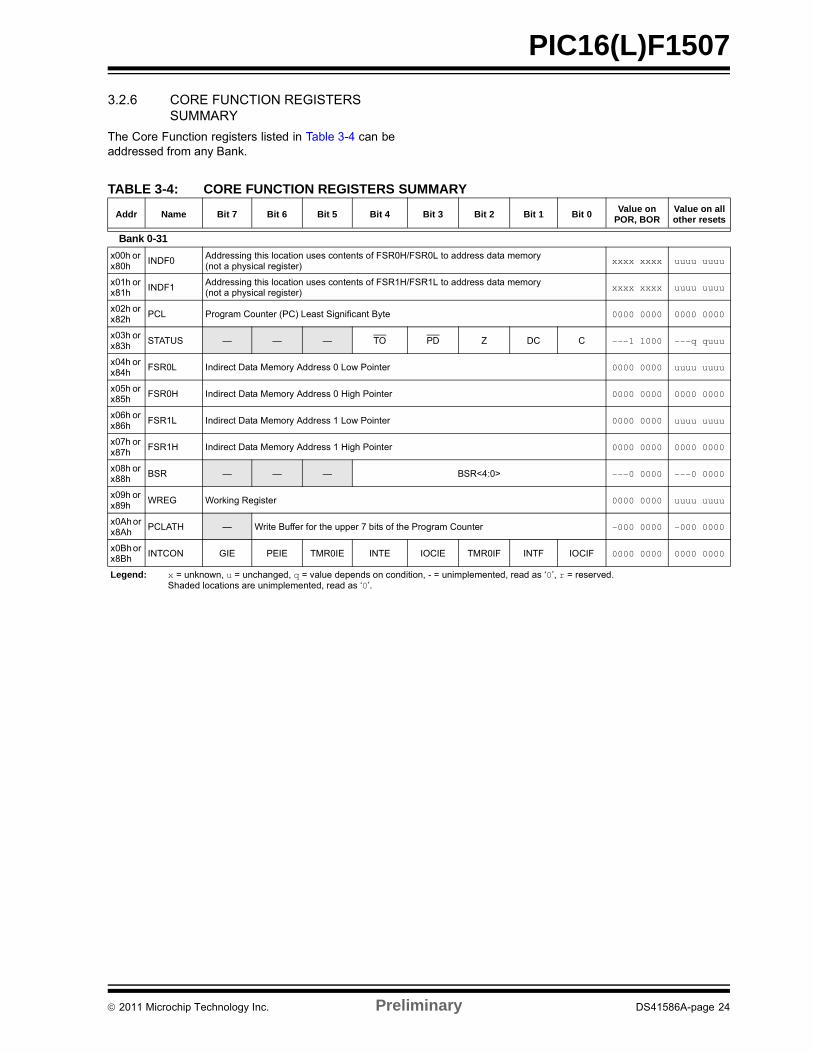
3.2.6 CORE FUNCTION REGISTERS SUMMARY
The Core Function registers listed in Table 3-4 can beaddressed from any Bank.
TABLE 3-4: CORE FUNCTION REGISTERS SUMMARY
Addr Name Bit 7 Bit 6 Bit 5 Bit 4 Bit 3 Bit 2 Bit 1 Bit 0Value on
POR, BORValue on all other resets
Bank 0-31
x00h or x80h
INDF0Addressing this location uses contents of FSR0H/FSR0L to address data memory(not a physical register)
xxxx xxxx uuuu uuuu
x01h or x81h
INDF1Addressing this location uses contents of FSR1H/FSR1L to address data memory(not a physical register)
xxxx xxxx uuuu uuuu
x02h or x82h
PCL Program Counter (PC) Least Significant Byte 0000 0000 0000 0000
x03h or x83h
STATUS — — — TO PD Z DC C ---1 1000 ---q quuu
x04h or x84h
FSR0L Indirect Data Memory Address 0 Low Pointer 0000 0000 uuuu uuuu
x05h or x85h
FSR0H Indirect Data Memory Address 0 High Pointer 0000 0000 0000 0000
x06h or x86h
FSR1L Indirect Data Memory Address 1 Low Pointer 0000 0000 uuuu uuuu
x07h or x87h
FSR1H Indirect Data Memory Address 1 High Pointer 0000 0000 0000 0000
x08h or x88h
BSR — — — BSR<4:0> ---0 0000 ---0 0000
x09h or x89h
WREG Working Register 0000 0000 uuuu uuuu
x0Ah or x8Ah
PCLATH — Write Buffer for the upper 7 bits of the Program Counter -000 0000 -000 0000
x0Bh or x8Bh
INTCON GIE PEIE TMR0IE INTE IOCIE TMR0IF INTF IOCIF 0000 0000 0000 0000
Legend: x = unknown, u = unchanged, q = value depends on condition, - = unimplemented, read as ‘0’, r = reserved. Shaded locations are unimplemented, read as ‘0’.
2011 Microchip Technology Inc. Preliminary DS41586A-page 24
PIC16(L)F1507
n all r ts
xxx
---
xxx
-00
0--
-00
uuu
uuu
uuu
u-u
x-u
000
111
000
111
---
111
-00
0--
-00
111
quu
110
-00
uuu
uuu
000
-00
---
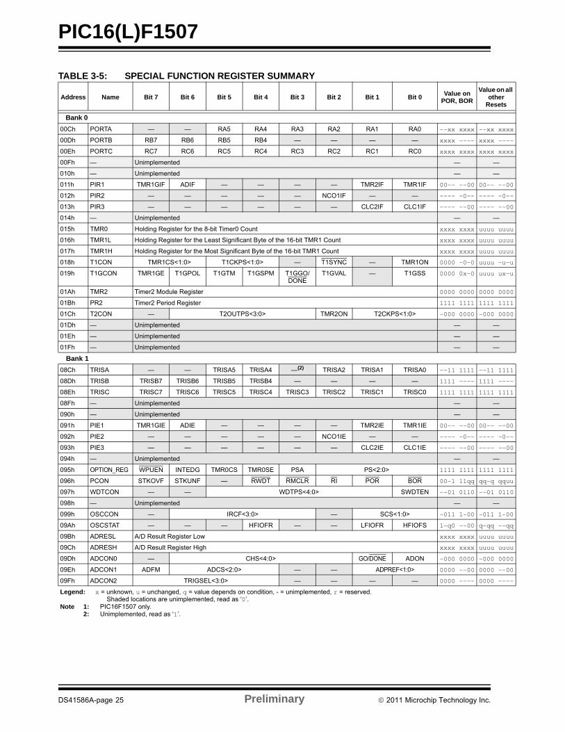
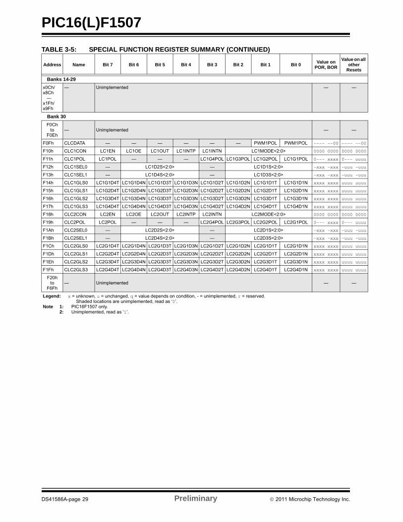
TABLE 3-5: SPECIAL FUNCTION REGISTER SUMMARY
Address Name Bit 7 Bit 6 Bit 5 Bit 4 Bit 3 Bit 2 Bit 1 Bit 0Value on
POR, BOR
Value oothe
Rese
Bank 0
00Ch PORTA — — RA5 RA4 RA3 RA2 RA1 RA0 --xx xxxx --xx x
00Dh PORTB RB7 RB6 RB5 RB4 — — — — xxxx ---- xxxx -
00Eh PORTC RC7 RC6 RC5 RC4 RC3 RC2 RC1 RC0 xxxx xxxx xxxx x
00Fh — Unimplemented — —
010h — Unimplemented — —
011h PIR1 TMR1GIF ADIF — — — — TMR2IF TMR1IF 00-- --00 00-- -
012h PIR2 — — — — — NCO1IF — — ---- -0-- ---- -
013h PIR3 — — — — — — CLC2IF CLC1IF ---- --00 ---- -
014h — Unimplemented — —
015h TMR0 Holding Register for the 8-bit Timer0 Count xxxx xxxx uuuu u
016h TMR1L Holding Register for the Least Significant Byte of the 16-bit TMR1 Count xxxx xxxx uuuu u
017h TMR1H Holding Register for the Most Significant Byte of the 16-bit TMR1 Count xxxx xxxx uuuu u
018h T1CON TMR1CS<1:0> T1CKPS<1:0> — T1SYNC — TMR1ON 0000 -0-0 uuuu -
019h T1GCON TMR1GE T1GPOL T1GTM T1GSPM T1GGO/DONE
T1GVAL — T1GSS 0000 0x-0 uuuu u
01Ah TMR2 Timer2 Module Register 0000 0000 0000 0
01Bh PR2 Timer2 Period Register 1111 1111 1111 1
01Ch T2CON — T2OUTPS<3:0> TMR2ON T2CKPS<1:0> -000 0000 -000 0
01Dh — Unimplemented — —
01Eh — Unimplemented — —
01Fh — Unimplemented — —
Bank 1
08Ch TRISA — — TRISA5 TRISA4 —(2) TRISA2 TRISA1 TRISA0 --11 1111 --11 1
08Dh TRISB TRISB7 TRISB6 TRISB5 TRISB4 — — — — 1111 ---- 1111 -
08Eh TRISC TRISC7 TRISC6 TRISC5 TRISC4 TRISC3 TRISC2 TRISC1 TRISC0 1111 1111 1111 1
08Fh — Unimplemented — —
090h — Unimplemented — —
091h PIE1 TMR1GIE ADIE — — — — TMR2IE TMR1IE 00-- --00 00-- -
092h PIE2 — — — — — NCO1IE — — ---- -0-- ---- -
093h PIE3 — — — — — — CLC2IE CLC1IE ---- --00 ---- -
094h — Unimplemented — —
095h OPTION_REG WPUEN INTEDG TMR0CS TMR0SE PSA PS<2:0> 1111 1111 1111 1
096h PCON STKOVF STKUNF — RWDT RMCLR RI POR BOR 00-1 11qq qq-q q
097h WDTCON — — WDTPS<4:0> SWDTEN --01 0110 --01 0
098h — Unimplemented — —
099h OSCCON — IRCF<3:0> — SCS<1:0> -011 1-00 -011 1
09Ah OSCSTAT — — — HFIOFR — — LFIOFR HFIOFS 1-q0 --00 q-qq -
09Bh ADRESL A/D Result Register Low xxxx xxxx uuuu u
09Ch ADRESH A/D Result Register High xxxx xxxx uuuu u
09Dh ADCON0 — CHS<4:0> GO/DONE ADON -000 0000 -000 0
09Eh ADCON1 ADFM ADCS<2:0> — — ADPREF<1:0> 0000 --00 0000 -
09Fh ADCON2 TRIGSEL<3:0> — — — — 0000 ---- 0000 -
Legend: x = unknown, u = unchanged, q = value depends on condition, - = unimplemented, r = reserved. Shaded locations are unimplemented, read as ‘0’.
Note 1: PIC16F1507 only.2: Unimplemented, read as ‘1’.
DS41586A-page 25 Preliminary 2011 Microchip Technology Inc.
PIC16(L)F1507
uuu
---
uuu
--u
-00
-00
111
---
111
000
000
uuu
uuu
000
000
-01
111
---
n all r ts
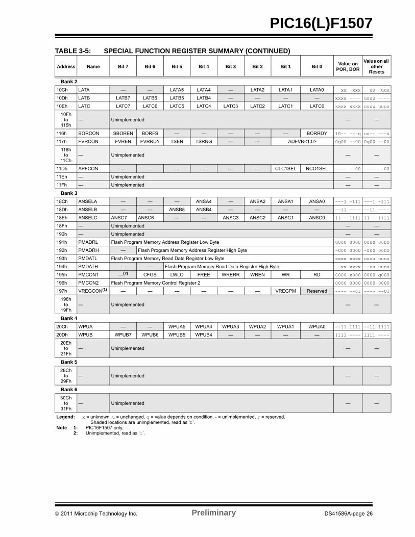
Bank 2
10Ch LATA — — LATA5 LATA4 — LATA2 LATA1 LATA0 --xx -xxx --uu -
10Dh LATB LATB7 LATB6 LATB5 LATB4 — — — — xxxx ---- uuuu -
10Eh LATC LATC7 LATC6 LATC5 LATC4 LATC3 LATC2 LATC1 LATC0 xxxx xxxx uuuu u
10Fhto
115h— Unimplemented — —
116h BORCON SBOREN BORFS — — — — — BORRDY 10-- ---q uu-- -
117h FVRCON FVREN FVRRDY TSEN TSRNG — — ADFVR<1:0> 0q00 --00 0q00 -
118hto
11Ch— Unimplemented — —
11Dh APFCON — — — — — — CLC1SEL NCO1SEL ---- --00 ---- -
11Eh — Unimplemented — —
11Fh — Unimplemented — —
Bank 3
18Ch ANSELA — — — ANSA4 — ANSA2 ANSA1 ANSA0 ---1 -111 ---1 -
18Dh ANSELB — — ANSB5 ANSB4 — — — — --11 ---- --11 -
18Eh ANSELC ANSC7 ANSC6 — — ANSC3 ANSC2 ANSC1 ANSC0 11-- 1111 11-- 1
18Fh — Unimplemented — —
190h — Unimplemented — —
191h PMADRL Flash Program Memory Address Register Low Byte 0000 0000 0000 0
192h PMADRH — Flash Program Memory Address Register High Byte -000 0000 -000 0
193h PMDATL Flash Program Memory Read Data Register Low Byte xxxx xxxx uuuu u
194h PMDATH — — Flash Program Memory Read Data Register High Byte --xx xxxx --uu u
195h PMCON1 —(2) CFGS LWLO FREE WRERR WREN WR RD 0000 x000 0000 q
196h PMCON2 Flash Program Memory Control Register 2 0000 0000 0000 0
197h VREGCON(1) — — — — — — VREGPM Reserved ---- --01 ---- -
198hto
19Fh— Unimplemented — —
Bank 4
20Ch WPUA — — WPUA5 WPUA4 WPUA3 WPUA2 WPUA1 WPUA0 --11 1111 --11 1
20Dh WPUB WPUB7 WPUB6 WPUB5 WPUB4 — — — — 1111 ---- 1111 -
20Ehto
21Fh— Unimplemented — —
Bank 5
28Chto
29Fh— Unimplemented — —
Bank 6
30Chto
31Fh— Unimplemented — —
TABLE 3-5: SPECIAL FUNCTION REGISTER SUMMARY (CONTINUED)
Address Name Bit 7 Bit 6 Bit 5 Bit 4 Bit 3 Bit 2 Bit 1 Bit 0Value on
POR, BOR
Value oothe
Rese
Legend: x = unknown, u = unchanged, q = value depends on condition, - = unimplemented, r = reserved. Shaded locations are unimplemented, read as ‘0’.
Note 1: PIC16F1507 only.2: Unimplemented, read as ‘1’.
2011 Microchip Technology Inc. Preliminary DS41586A-page 26
PIC16(L)F1507
000
000
000
---
---
---
000
000
000
000
000
--0
-00
n all r ts
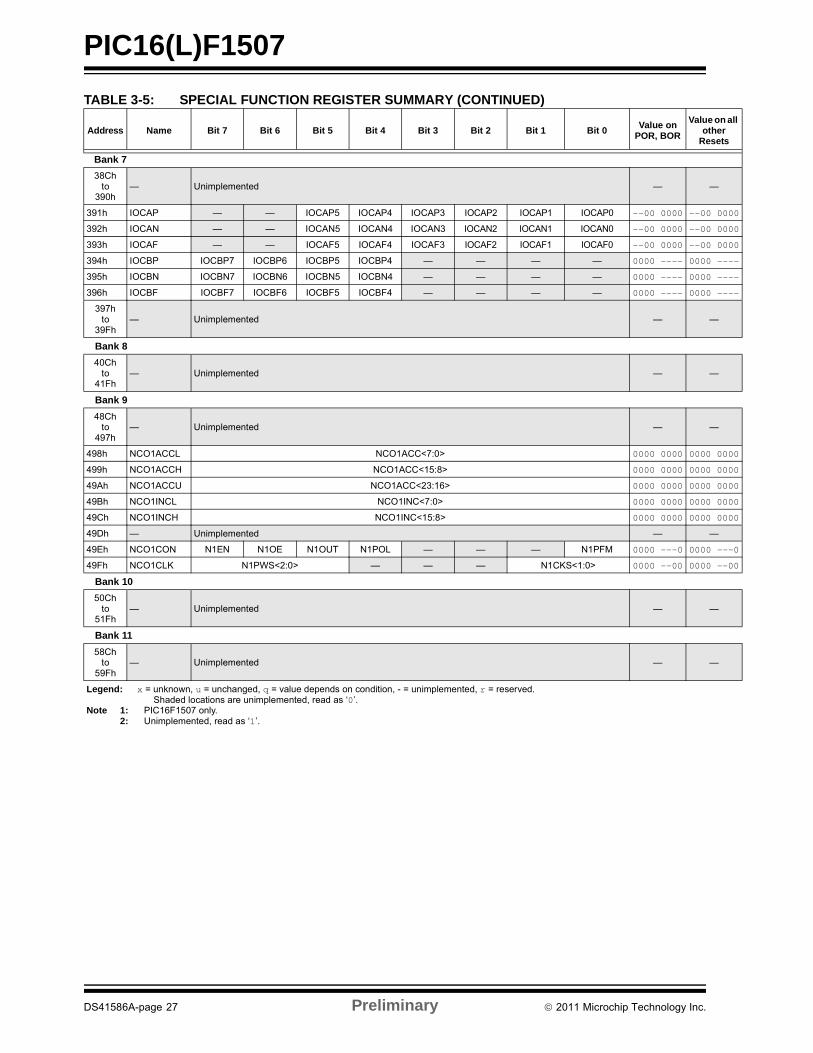
Bank 7
38Chto
390h— Unimplemented — —
391h IOCAP — — IOCAP5 IOCAP4 IOCAP3 IOCAP2 IOCAP1 IOCAP0 --00 0000 --00 0
392h IOCAN — — IOCAN5 IOCAN4 IOCAN3 IOCAN2 IOCAN1 IOCAN0 --00 0000 --00 0
393h IOCAF — — IOCAF5 IOCAF4 IOCAF3 IOCAF2 IOCAF1 IOCAF0 --00 0000 --00 0
394h IOCBP IOCBP7 IOCBP6 IOCBP5 IOCBP4 — — — — 0000 ---- 0000 -
395h IOCBN IOCBN7 IOCBN6 IOCBN5 IOCBN4 — — — — 0000 ---- 0000 -
396h IOCBF IOCBF7 IOCBF6 IOCBF5 IOCBF4 — — — — 0000 ---- 0000 -
397hto
39Fh— Unimplemented — —
Bank 8
40Chto
41Fh— Unimplemented — —
Bank 9
48Chto
497h— Unimplemented — —
498h NCO1ACCL NCO1ACC<7:0> 0000 0000 0000 0
499h NCO1ACCH NCO1ACC<15:8> 0000 0000 0000 0
49Ah NCO1ACCU NCO1ACC<23:16> 0000 0000 0000 0
49Bh NCO1INCL NCO1INC<7:0> 0000 0000 0000 0
49Ch NCO1INCH NCO1INC<15:8> 0000 0000 0000 0
49Dh — Unimplemented — —
49Eh NCO1CON N1EN N1OE N1OUT N1POL — — — N1PFM 0000 ---0 0000 -
49Fh NCO1CLK N1PWS<2:0> — — — N1CKS<1:0> 0000 --00 0000 -
Bank 10
50Chto
51Fh— Unimplemented — —
Bank 11
58Chto
59Fh— Unimplemented — —
TABLE 3-5: SPECIAL FUNCTION REGISTER SUMMARY (CONTINUED)
Address Name Bit 7 Bit 6 Bit 5 Bit 4 Bit 3 Bit 2 Bit 1 Bit 0Value on
POR, BOR
Value oothe
Rese
Legend: x = unknown, u = unchanged, q = value depends on condition, - = unimplemented, r = reserved. Shaded locations are unimplemented, read as ‘0’.
Note 1: PIC16F1507 only.2: Unimplemented, read as ‘1’.
DS41586A-page 27 Preliminary 2011 Microchip Technology Inc.
PIC16(L)F1507
---
uuu
---
---
uuu
---
---
uuu
---
---
uuu
---
000
xxx
--0
000
-00
n all r ts
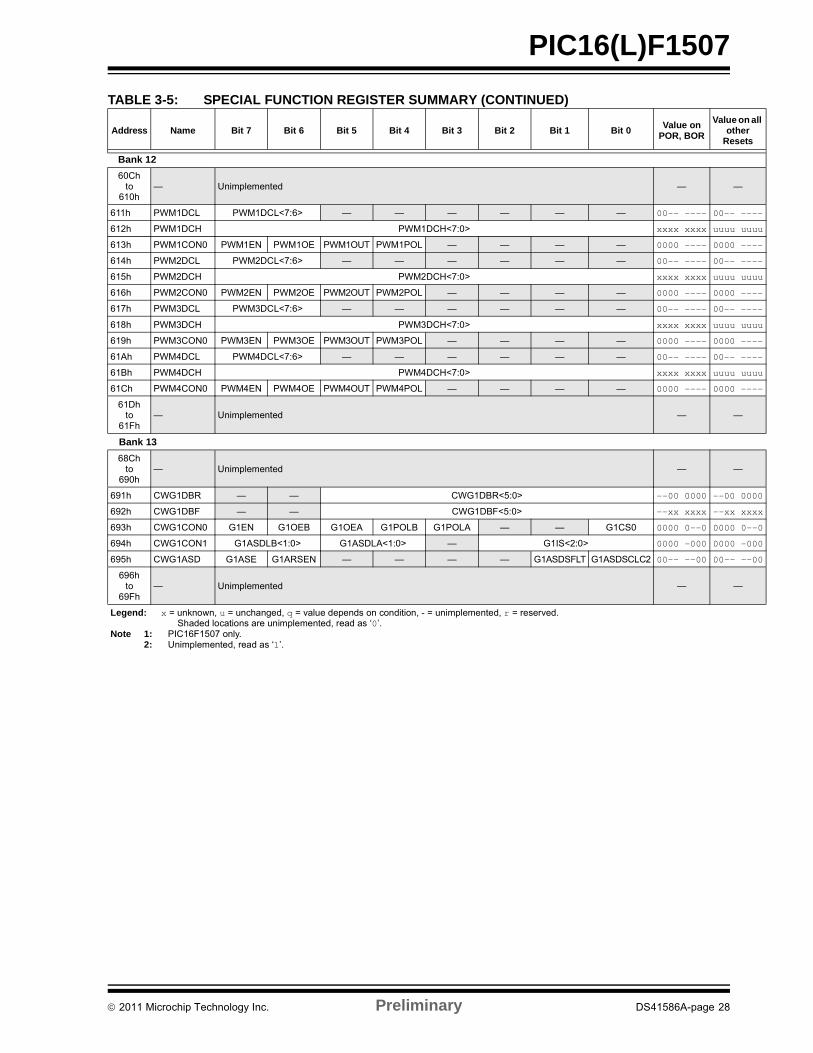
Bank 12
60Chto
610h— Unimplemented — —
611h PWM1DCL PWM1DCL<7:6> — — — — — — 00-- ---- 00-- -
612h PWM1DCH PWM1DCH<7:0> xxxx xxxx uuuu u
613h PWM1CON0 PWM1EN PWM1OE PWM1OUT PWM1POL — — — — 0000 ---- 0000 -
614h PWM2DCL PWM2DCL<7:6> — — — — — — 00-- ---- 00-- -
615h PWM2DCH PWM2DCH<7:0> xxxx xxxx uuuu u
616h PWM2CON0 PWM2EN PWM2OE PWM2OUT PWM2POL — — — — 0000 ---- 0000 -
617h PWM3DCL PWM3DCL<7:6> — — — — — — 00-- ---- 00-- -
618h PWM3DCH PWM3DCH<7:0> xxxx xxxx uuuu u
619h PWM3CON0 PWM3EN PWM3OE PWM3OUT PWM3POL — — — — 0000 ---- 0000 -
61Ah PWM4DCL PWM4DCL<7:6> — — — — — — 00-- ---- 00-- -
61Bh PWM4DCH PWM4DCH<7:0> xxxx xxxx uuuu u
61Ch PWM4CON0 PWM4EN PWM4OE PWM4OUT PWM4POL — — — — 0000 ---- 0000 -
61Dhto
61Fh— Unimplemented — —
Bank 13
68Chto
690h— Unimplemented — —
691h CWG1DBR — — CWG1DBR<5:0> --00 0000 --00 0
692h CWG1DBF — — CWG1DBF<5:0> --xx xxxx --xx x
693h CWG1CON0 G1EN G1OEB G1OEA G1POLB G1POLA — — G1CS0 0000 0--0 0000 0
694h CWG1CON1 G1ASDLB<1:0> G1ASDLA<1:0> — G1IS<2:0> 0000 -000 0000 -
695h CWG1ASD G1ASE G1ARSEN — — — — G1ASDSFLT G1ASDSCLC2 00-- --00 00-- -
696hto
69Fh— Unimplemented — —
TABLE 3-5: SPECIAL FUNCTION REGISTER SUMMARY (CONTINUED)
Address Name Bit 7 Bit 6 Bit 5 Bit 4 Bit 3 Bit 2 Bit 1 Bit 0Value on
POR, BOR
Value oothe
Rese
Legend: x = unknown, u = unchanged, q = value depends on condition, - = unimplemented, r = reserved. Shaded locations are unimplemented, read as ‘0’.
Note 1: PIC16F1507 only.2: Unimplemented, read as ‘1’.
2011 Microchip Technology Inc. Preliminary DS41586A-page 28
PIC16(L)F1507
-00
000
uuu
uuu
uuu
uuu
uuu
uuu
uuu
000
uuu
uuu
uuu
uuu
uuu
uuu
uuu
n all r ts
Banks 14-29
x0Ch/x8Ch —x1Fh/x9Fh
— Unimplemented — —
Bank 30
F0Chto
F0Eh— Unimplemented — —
F0Fh CLCDATA — — — — — — PWM1POL PWM1POL ---- --00 ---- -
F10h CLC1CON LC1EN LC1OE LC1OUT LC1INTP LC1INTN LC1MODE<2:0> 0000 0000 0000 0
F11h CLC1POL LC1POL — — — LC1G4POL LC1G3POL LC1G2POL LC1G1POL 0--- xxxx 0--- u
F12h CLC1SEL0 — LC1D2S<2:0> — LC1D1S<2:0> -xxx -xxx -uuu -
F13h CLC1SEL1 — LC1D4S<2:0> — LC1D3S<2:0> -xxx -xxx -uuu -
F14h CLC1GLS0 LC1G1D4T LC1G1D4N LC1G1D3T LC1G1D3N LC1G1D2T LC1G1D2N LC1G1D1T LC1G1D1N xxxx xxxx uuuu u
F15h CLC1GLS1 LC1G2D4T LC1G2D4N LC1G2D3T LC1G2D3N LC1G2D2T LC1G2D2N LC1G2D1T LC1G2D1N xxxx xxxx uuuu u
F16h CLC1GLS2 LC1G3D4T LC1G3D4N LC1G3D3T LC1G3D3N LC1G3D2T LC1G3D2N LC1G3D1T LC1G3D1N xxxx xxxx uuuu u
F17h CLC1GLS3 LC1G4D4T LC1G4D4N LC1G4D3T LC1G4D3N LC1G4D2T LC1G4D2N LC1G4D1T LC1G4D1N xxxx xxxx uuuu u
F18h CLC2CON LC2EN LC2OE LC2OUT LC2INTP LC2INTN LC2MODE<2:0> 0000 0000 0000 0
F19h CLC2POL LC2POL — — — LC2G4POL LC2G3POL LC2G2POL LC2G1POL 0--- xxxx 0--- u
F1Ah CLC2SEL0 — LC2D2S<2:0> — LC2D1S<2:0> -xxx -xxx -uuu -
F1Bh CLC2SEL1 — LC2D4S<2:0> — LC2D3S<2:0> -xxx -xxx -uuu -
F1Ch CLC2GLS0 LC2G1D4T LC2G1D4N LC2G1D3T LC2G1D3N LC2G1D2T LC2G1D2N LC2G1D1T LC2G1D1N xxxx xxxx uuuu u
F1Dh CLC2GLS1 LC2G2D4T LC2G2D4N LC2G2D3T LC2G2D3N LC2G2D2T LC2G2D2N LC2G2D1T LC2G2D1N xxxx xxxx uuuu u
F1Eh CLC2GLS2 LC2G3D4T LC2G3D4N LC2G3D3T LC2G3D3N LC2G3D2T LC2G3D2N LC2G3D1T LC2G3D1N xxxx xxxx uuuu u
F1Fh CLC2GLS3 LC2G4D4T LC2G4D4N LC2G4D3T LC2G4D3N LC2G4D2T LC2G4D2N LC2G4D1T LC2G4D1N xxxx xxxx uuuu u
F20hto
F6Fh— Unimplemented — —
TABLE 3-5: SPECIAL FUNCTION REGISTER SUMMARY (CONTINUED)
Address Name Bit 7 Bit 6 Bit 5 Bit 4 Bit 3 Bit 2 Bit 1 Bit 0Value on
POR, BOR
Value oothe
Rese
Legend: x = unknown, u = unchanged, q = value depends on condition, - = unimplemented, r = reserved. Shaded locations are unimplemented, read as ‘0’.
Note 1: PIC16F1507 only.2: Unimplemented, read as ‘1’.
DS41586A-page 29 Preliminary 2011 Microchip Technology Inc.
PIC16(L)F1507
uuu
uuu
uuu
uuu
uuu
uuu
uuu
uuu
111
uuu
uuu
n all r ts
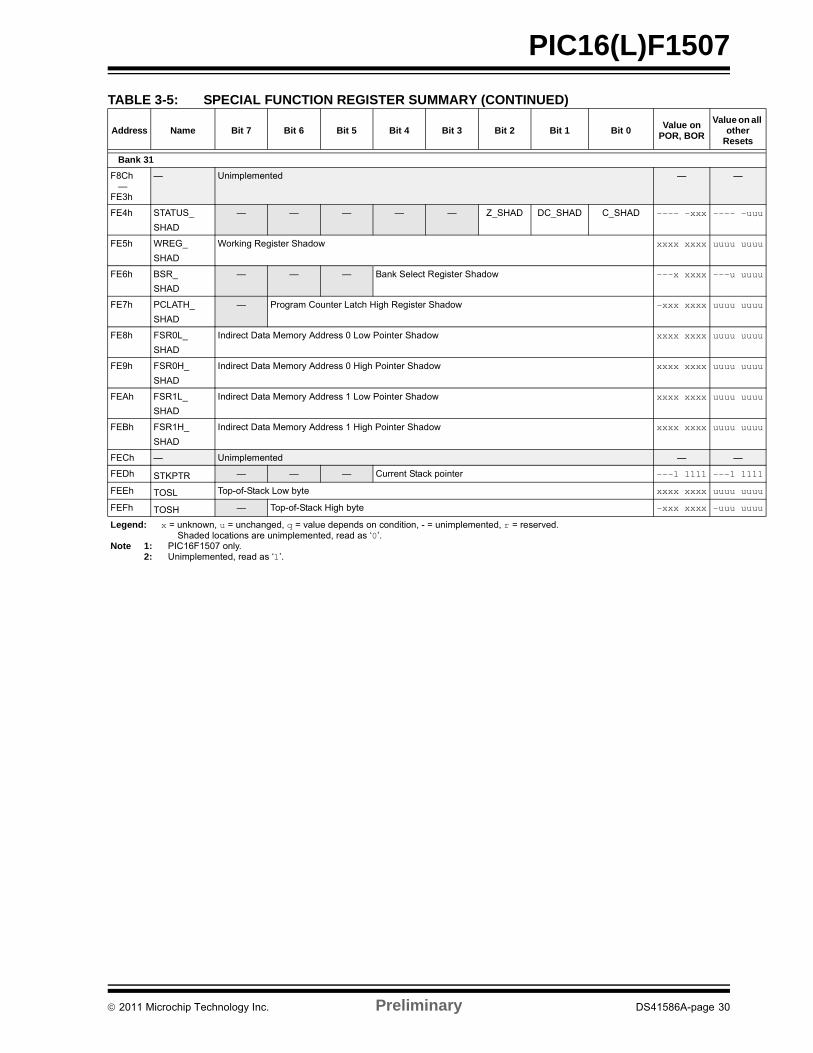
Bank 31
F8Ch —FE3h
— Unimplemented — —
FE4h STATUS_
SHAD
— — — — — Z_SHAD DC_SHAD C_SHAD ---- -xxx ---- -
FE5h WREG_
SHAD
Working Register Shadow xxxx xxxx uuuu u
FE6h BSR_
SHAD
— — — Bank Select Register Shadow ---x xxxx ---u u
FE7h PCLATH_
SHAD
— Program Counter Latch High Register Shadow -xxx xxxx uuuu u
FE8h FSR0L_
SHAD
Indirect Data Memory Address 0 Low Pointer Shadow xxxx xxxx uuuu u
FE9h FSR0H_
SHAD
Indirect Data Memory Address 0 High Pointer Shadow xxxx xxxx uuuu u
FEAh FSR1L_
SHAD
Indirect Data Memory Address 1 Low Pointer Shadow xxxx xxxx uuuu u
FEBh FSR1H_
SHAD
Indirect Data Memory Address 1 High Pointer Shadow xxxx xxxx uuuu u
FECh — Unimplemented — —
FEDh STKPTR — — — Current Stack pointer ---1 1111 ---1 1
FEEh TOSL Top-of-Stack Low byte xxxx xxxx uuuu u
FEFh TOSH — Top-of-Stack High byte -xxx xxxx -uuu u
TABLE 3-5: SPECIAL FUNCTION REGISTER SUMMARY (CONTINUED)
Address Name Bit 7 Bit 6 Bit 5 Bit 4 Bit 3 Bit 2 Bit 1 Bit 0Value on
POR, BOR
Value oothe
Rese
Legend: x = unknown, u = unchanged, q = value depends on condition, - = unimplemented, r = reserved. Shaded locations are unimplemented, read as ‘0’.
Note 1: PIC16F1507 only.2: Unimplemented, read as ‘1’.
2011 Microchip Technology Inc. Preliminary DS41586A-page 30
PIC16(L)F1507
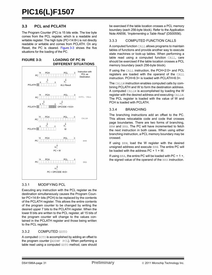
3.3 PCL and PCLATH
The Program Counter (PC) is 15 bits wide. The low bytecomes from the PCL register, which is a readable andwritable register. The high byte (PC<14:8>) is not directlyreadable or writable and comes from PCLATH. On anyReset, the PC is cleared. Figure 3-3 shows the fivesituations for the loading of the PC.
FIGURE 3-3: LOADING OF PC IN DIFFERENT SITUATIONS
3.3.1 MODIFYING PCL
Executing any instruction with the PCL register as thedestination simultaneously causes the Program Coun-ter PC<14:8> bits (PCH) to be replaced by the contentsof the PCLATH register. This allows the entire contentsof the program counter to be changed by writing thedesired upper 7 bits to the PCLATH register. When thelower 8 bits are written to the PCL register, all 15 bits ofthe program counter will change to the values con-tained in the PCLATH register and those being writtento the PCL register.
3.3.2 COMPUTED GOTO
A computed GOTO is accomplished by adding an offset tothe program counter (ADDWF PCL). When performing atable read using a computed GOTO method, care should
be exercised if the table location crosses a PCL memoryboundary (each 256-byte block). Refer to the ApplicationNote AN556, “Implementing a Table Read” (DS00556).
3.3.3 COMPUTED FUNCTION CALLS
A computed function CALL allows programs to maintaintables of functions and provide another way to executestate machines or look-up tables. When performing atable read using a computed function CALL, careshould be exercised if the table location crosses a PCLmemory boundary (each 256-byte block).
If using the CALL instruction, the PCH<2:0> and PCLregisters are loaded with the operand of the CALLinstruction. PCH<6:3> is loaded with PCLATH<6:3>.
The CALLW instruction enables computed calls by com-bining PCLATH and W to form the destination address.A computed CALLW is accomplished by loading the Wregister with the desired address and executing CALLW.The PCL register is loaded with the value of W andPCH is loaded with PCLATH.
3.3.4 BRANCHING
The branching instructions add an offset to the PC.This allows relocatable code and code that crossespage boundaries. There are two forms of branching,BRW and BRA. The PC will have incremented to fetchthe next instruction in both cases. When using eitherbranching instruction, a PCL memory boundary may becrossed.
If using BRW, load the W register with the desiredunsigned address and execute BRW. The entire PC willbe loaded with the address PC + 1 + W.
If using BRA, the entire PC will be loaded with PC + 1 +,the signed value of the operand of the BRA instruction.
PCLPCH 014
PC
PCLPCH 014
PC
ALU Result
876
PCLATH0
Instruction withPCL as
Destination
GOTO, CALL
OPCODE <10:0>
1146
PCLATH0
PCLPCH 014
PC
W
876
PCLATH0
CALLW
PCLPCH 014
PC
PC + W
15
BRW
PCLPCH 014
PC
PC + OPCODE <8:0>
15
BRA
DS41586A-page 31 Preliminary 2011 Microchip Technology Inc.
PIC16(L)F1507
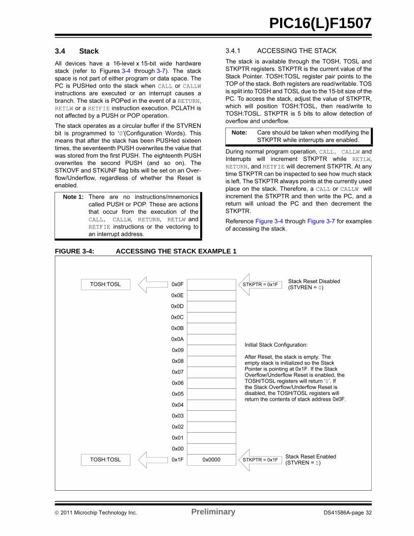
3.4 Stack
All devices have a 16-level x 15-bit wide hardwarestack (refer to Figures 3-4 through 3-7). The stackspace is not part of either program or data space. ThePC is PUSHed onto the stack when CALL or CALLWinstructions are executed or an interrupt causes abranch. The stack is POPed in the event of a RETURN,RETLW or a RETFIE instruction execution. PCLATH isnot affected by a PUSH or POP operation.
The stack operates as a circular buffer if the STVRENbit is programmed to ‘0‘(Configuration Words). Thismeans that after the stack has been PUSHed sixteentimes, the seventeenth PUSH overwrites the value thatwas stored from the first PUSH. The eighteenth PUSHoverwrites the second PUSH (and so on). TheSTKOVF and STKUNF flag bits will be set on an Over-flow/Underflow, regardless of whether the Reset isenabled.
3.4.1 ACCESSING THE STACK
The stack is available through the TOSH, TOSL andSTKPTR registers. STKPTR is the current value of theStack Pointer. TOSH:TOSL register pair points to theTOP of the stack. Both registers are read/writable. TOSis split into TOSH and TOSL due to the 15-bit size of thePC. To access the stack, adjust the value of STKPTR,which will position TOSH:TOSL, then read/write toTOSH:TOSL. STKPTR is 5 bits to allow detection ofoverflow and underflow.
During normal program operation, CALL, CALLW andInterrupts will increment STKPTR while RETLW,RETURN, and RETFIE will decrement STKPTR. At anytime STKPTR can be inspected to see how much stackis left. The STKPTR always points at the currently usedplace on the stack. Therefore, a CALL or CALLW willincrement the STKPTR and then write the PC, and areturn will unload the PC and then decrement theSTKPTR.
Reference Figure 3-4 through Figure 3-7 for examplesof accessing the stack.
FIGURE 3-4: ACCESSING THE STACK EXAMPLE 1
Note 1: There are no instructions/mnemonicscalled PUSH or POP. These are actionsthat occur from the execution of theCALL, CALLW, RETURN, RETLW andRETFIE instructions or the vectoring toan interrupt address.
Note: Care should be taken when modifying theSTKPTR while interrupts are enabled.
0x0F
0x0E
0x0D
0x0C
0x0B
0x0A
0x09
0x08
0x07
0x06
0x05
0x04
0x03
0x02
0x01
0x00
0x0000
STKPTR = 0x1F
Initial Stack Configuration:
After Reset, the stack is empty. Theempty stack is initialized so the StackPointer is pointing at 0x1F. If the StackOverflow/Underflow Reset is enabled, theTOSH/TOSL registers will return ‘0’. Ifthe Stack Overflow/Underflow Reset isdisabled, the TOSH/TOSL registers willreturn the contents of stack address 0x0F.
0x1F STKPTR = 0x1F
Stack Reset Disabled(STVREN = 0)
Stack Reset Enabled(STVREN = 1)
TOSH:TOSL
TOSH:TOSL
2011 Microchip Technology Inc. Preliminary DS41586A-page 32
PIC16(L)F1507
FIGURE 3-5: ACCESSING THE STACK EXAMPLE 2
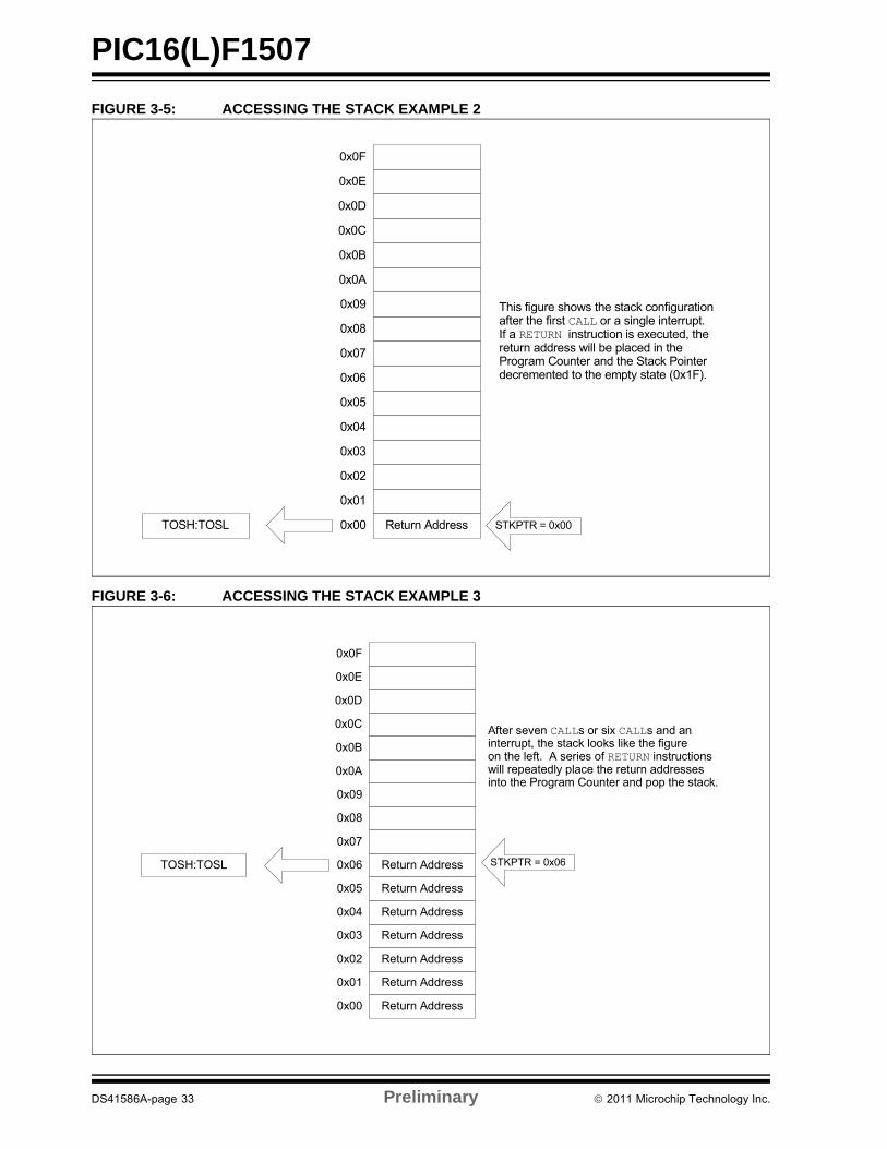
FIGURE 3-6: ACCESSING THE STACK EXAMPLE 3
0x0F
0x0E
0x0D
0x0C
0x0B
0x0A
0x09
0x08
0x07
0x06
0x05
0x04
0x03
0x02
0x01
Return Address0x00 STKPTR = 0x00
This figure shows the stack configurationafter the first CALL or a single interrupt.If a RETURN instruction is executed, thereturn address will be placed in theProgram Counter and the Stack Pointerdecremented to the empty state (0x1F).
TOSH:TOSL
0x0F
0x0E
0x0D
0x0C
0x0B
0x0A
0x09
0x08
0x07
Return Address0x06
Return Address0x05
Return Address0x04
Return Address0x03
Return Address0x02
Return Address0x01
Return Address0x00
STKPTR = 0x06
After seven CALLs or six CALLs and aninterrupt, the stack looks like the figureon the left. A series of RETURN instructionswill repeatedly place the return addresses into the Program Counter and pop the stack.
TOSH:TOSL
DS41586A-page 33 Preliminary 2011 Microchip Technology Inc.
PIC16(L)F1507
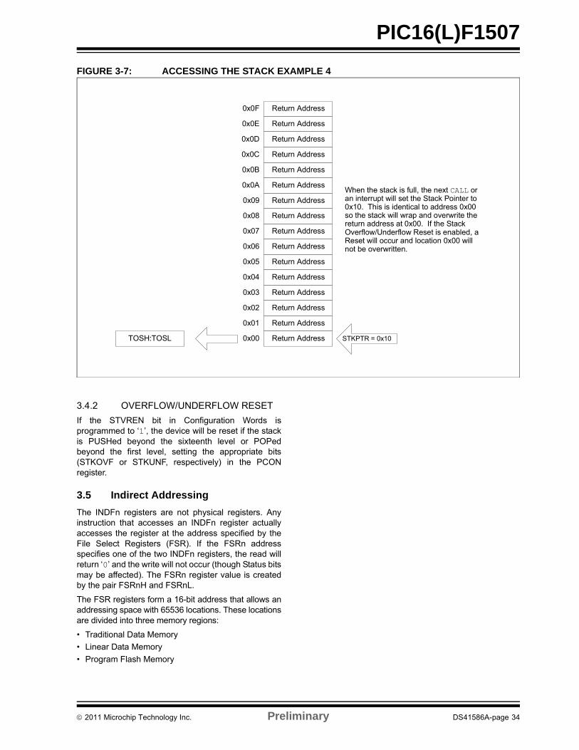
FIGURE 3-7: ACCESSING THE STACK EXAMPLE 4
3.4.2 OVERFLOW/UNDERFLOW RESET
If the STVREN bit in Configuration Words isprogrammed to ‘1’, the device will be reset if the stackis PUSHed beyond the sixteenth level or POPedbeyond the first level, setting the appropriate bits(STKOVF or STKUNF, respectively) in the PCONregister.
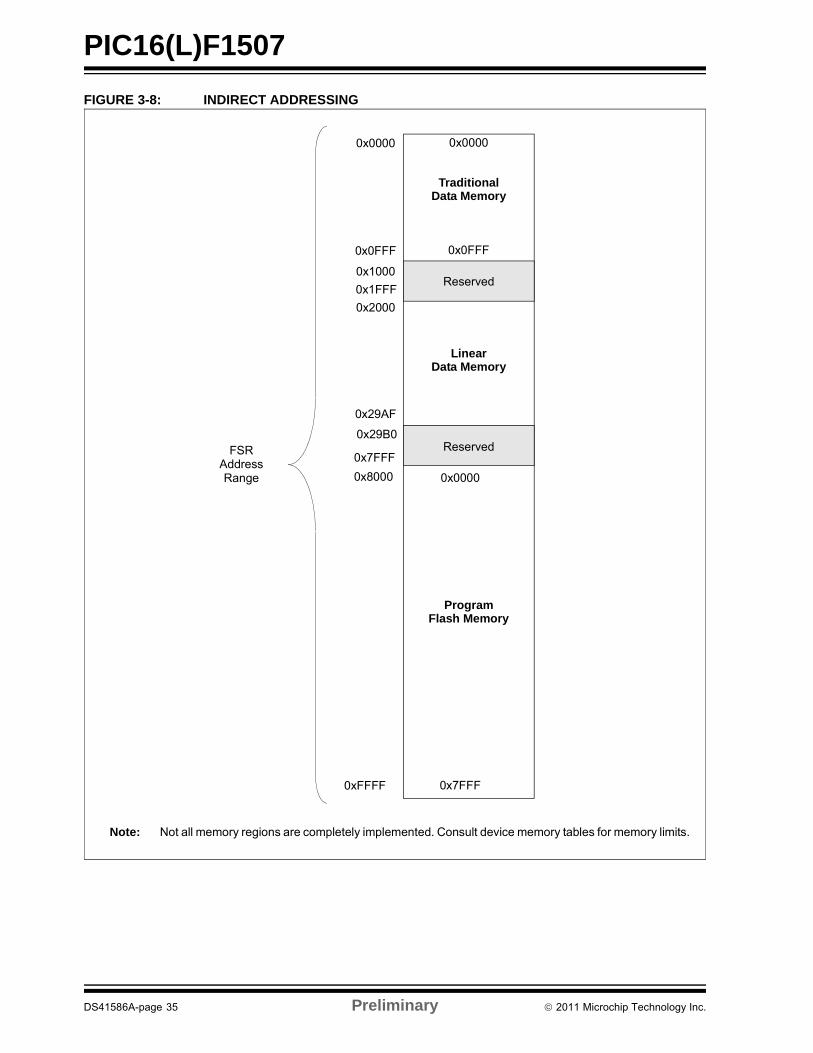
3.5 Indirect Addressing
The INDFn registers are not physical registers. Anyinstruction that accesses an INDFn register actuallyaccesses the register at the address specified by theFile Select Registers (FSR). If the FSRn addressspecifies one of the two INDFn registers, the read willreturn ‘0’ and the write will not occur (though Status bitsmay be affected). The FSRn register value is createdby the pair FSRnH and FSRnL.
The FSR registers form a 16-bit address that allows anaddressing space with 65536 locations. These locationsare divided into three memory regions:
• Traditional Data Memory
• Linear Data Memory
• Program Flash Memory
0x0F
0x0E
0x0D
0x0C
0x0B
0x0A
0x09
0x08
0x07
0x06
0x05
0x04
0x03
0x02
0x01
Return Address0x00 STKPTR = 0x10
When the stack is full, the next CALL oran interrupt will set the Stack Pointer to0x10. This is identical to address 0x00so the stack will wrap and overwrite thereturn address at 0x00. If the StackOverflow/Underflow Reset is enabled, aReset will occur and location 0x00 willnot be overwritten.
Return Address
Return Address
Return Address
Return Address
Return Address
Return Address
Return Address
Return Address
Return Address
Return Address
Return Address
Return Address
Return Address
Return Address
Return Address
TOSH:TOSL
2011 Microchip Technology Inc. Preliminary DS41586A-page 34
PIC16(L)F1507
FIGURE 3-8: INDIRECT ADDRESSING
0x0000
0x0FFF
Traditional
FSRAddressRange
Data Memory
0x1000Reserved
LinearData Memory
Reserved
0x2000
0x29AF
0x29B0
0x7FFF
0x8000
0xFFFF
0x0000
0x0FFF
0x0000
0x7FFF
ProgramFlash Memory
Note: Not all memory regions are completely implemented. Consult device memory tables for memory limits.
0x1FFF
DS41586A-page 35 Preliminary 2011 Microchip Technology Inc.
PIC16(L)F1507
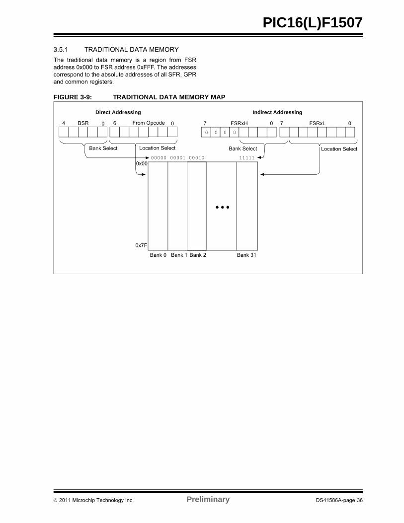
3.5.1 TRADITIONAL DATA MEMORY
The traditional data memory is a region from FSRaddress 0x000 to FSR address 0xFFF. The addressescorrespond to the absolute addresses of all SFR, GPRand common registers.
FIGURE 3-9: TRADITIONAL DATA MEMORY MAP
Indirect AddressingDirect Addressing
Bank Select Location Select
4 BSR 6 0From Opcode FSRxL7 0
Bank Select Location Select
00000 00001 00010 111110x00
0x7F
Bank 0 Bank 1 Bank 2 Bank 31
0 FSRxH7 0
0 0 0 0
2011 Microchip Technology Inc. Preliminary DS41586A-page 36
PIC16(L)F1507
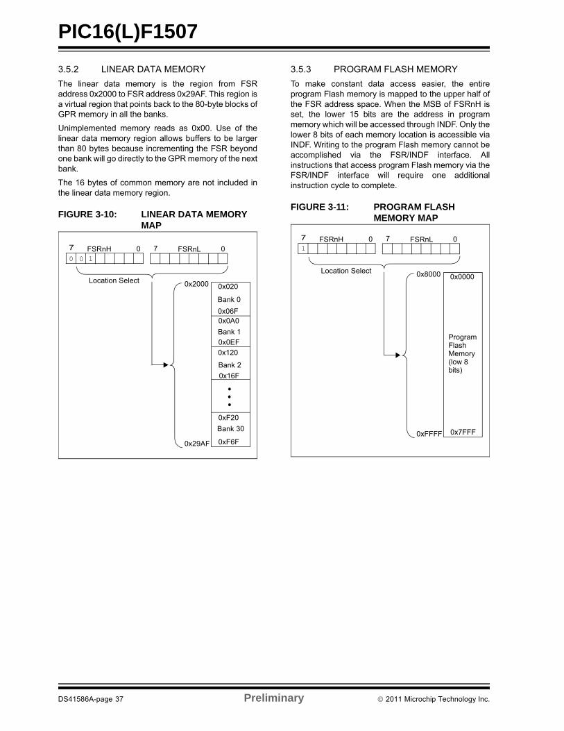
3.5.2 LINEAR DATA MEMORY
The linear data memory is the region from FSRaddress 0x2000 to FSR address 0x29AF. This region isa virtual region that points back to the 80-byte blocks ofGPR memory in all the banks.
Unimplemented memory reads as 0x00. Use of thelinear data memory region allows buffers to be largerthan 80 bytes because incrementing the FSR beyondone bank will go directly to the GPR memory of the nextbank.
The 16 bytes of common memory are not included inthe linear data memory region.
FIGURE 3-10: LINEAR DATA MEMORY MAP
3.5.3 PROGRAM FLASH MEMORY
To make constant data access easier, the entireprogram Flash memory is mapped to the upper half ofthe FSR address space. When the MSB of FSRnH isset, the lower 15 bits are the address in programmemory which will be accessed through INDF. Only thelower 8 bits of each memory location is accessible viaINDF. Writing to the program Flash memory cannot beaccomplished via the FSR/INDF interface. Allinstructions that access program Flash memory via theFSR/INDF interface will require one additionalinstruction cycle to complete.
FIGURE 3-11: PROGRAM FLASH MEMORY MAP
7
0 170 0
Location Select 0x2000
FSRnH FSRnL
0x020
Bank 0
0x06F0x0A0
Bank 1
0x0EF
0x120
Bank 2
0x16F
0xF20
Bank 30
0xF6F0x29AF
0
7
170 0
Location Select 0x8000
FSRnH FSRnL
0x0000
0x7FFF0xFFFF
ProgramFlashMemory(low 8bits)
DS41586A-page 37 Preliminary 2011 Microchip Technology Inc.

PIC16(L)F1507
NOTES:
2011 Microchip Technology Inc. Preliminary DS41586A-page 38
PIC16(L)F1507
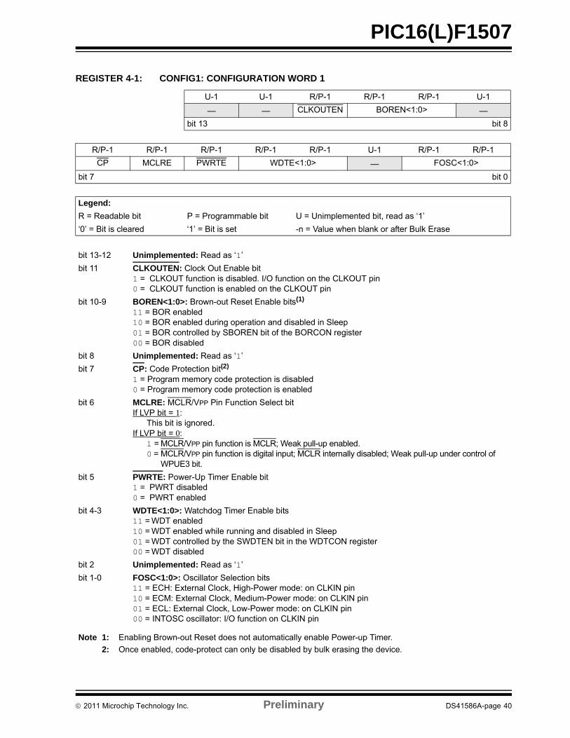
4.0 DEVICE CONFIGURATION
Device Configuration consists of Configuration Words,Code Protection and Device ID.
4.1 Configuration Words
There are several Configuration Word bits that allowdifferent oscillator and memory protection options.These are implemented as Configuration Word 1 at8007h and Configuration Word 2 at 8008h.
DS41586A-page 39 Preliminary 2011 Microchip Technology Inc.
PIC16(L)F1507
REGISTER 4-1: CONFIG1: CONFIGURATION WORD 1
U-1 U-1 R/P-1 R/P-1 R/P-1 U-1
— — CLKOUTEN BOREN<1:0> —
bit 13 bit 8
R/P-1 R/P-1 R/P-1 R/P-1 R/P-1 U-1 R/P-1 R/P-1
CP MCLRE PWRTE WDTE<1:0> — FOSC<1:0>
bit 7 bit 0
Legend:
R = Readable bit P = Programmable bit U = Unimplemented bit, read as ‘1’
‘0’ = Bit is cleared ‘1’ = Bit is set -n = Value when blank or after Bulk Erase
bit 13-12 Unimplemented: Read as ‘1’
bit 11 CLKOUTEN: Clock Out Enable bit1 = CLKOUT function is disabled. I/O function on the CLKOUT pin0 = CLKOUT function is enabled on the CLKOUT pin
bit 10-9 BOREN<1:0>: Brown-out Reset Enable bits(1)
11 = BOR enabled10 = BOR enabled during operation and disabled in Sleep01 = BOR controlled by SBOREN bit of the BORCON register00 = BOR disabled
bit 8 Unimplemented: Read as ‘1’
bit 7 CP: Code Protection bit(2)
1 = Program memory code protection is disabled0 = Program memory code protection is enabled
bit 6 MCLRE: MCLR/VPP Pin Function Select bitIf LVP bit = 1:
This bit is ignored.If LVP bit = 0:
1 = MCLR/VPP pin function is MCLR; Weak pull-up enabled.0 = MCLR/VPP pin function is digital input; MCLR internally disabled; Weak pull-up under control of
WPUE3 bit.
bit 5 PWRTE: Power-Up Timer Enable bit1 = PWRT disabled0 = PWRT enabled
bit 4-3 WDTE<1:0>: Watchdog Timer Enable bits11 = WDT enabled10 = WDT enabled while running and disabled in Sleep01 = WDT controlled by the SWDTEN bit in the WDTCON register00 = WDT disabled
bit 2 Unimplemented: Read as ‘1’
bit 1-0 FOSC<1:0>: Oscillator Selection bits11 = ECH: External Clock, High-Power mode: on CLKIN pin10 = ECM: External Clock, Medium-Power mode: on CLKIN pin01 = ECL: External Clock, Low-Power mode: on CLKIN pin00 = INTOSC oscillator: I/O function on CLKIN pin
Note 1: Enabling Brown-out Reset does not automatically enable Power-up Timer.
2: Once enabled, code-protect can only be disabled by bulk erasing the device.
2011 Microchip Technology Inc. Preliminary DS41586A-page 40
PIC16(L)F1507
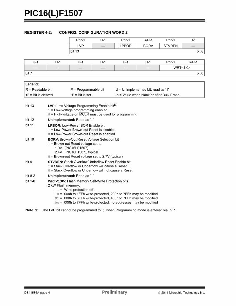
REGISTER 4-2: CONFIG2: CONFIGURATION WORD 2
R/P-1 U-1 R/P-1 R/P-1 R/P-1 U-1
LVP — LPBOR BORV STVREN —
bit 13 bit 8
U-1 U-1 U-1 U-1 U-1 U-1 R/P-1 R/P-1
— — — — — — WRT<1:0>
bit 7 bit 0
Legend:
R = Readable bit P = Programmable bit U = Unimplemented bit, read as ‘1’
‘0’ = Bit is cleared ‘1’ = Bit is set -n = Value when blank or after Bulk Erase
bit 13 LVP: Low-Voltage Programming Enable bit(1)
1 = Low-voltage programming enabled0 = High-voltage on MCLR must be used for programming
bit 12 Unimplemented: Read as ‘1’
bit 11 LPBOR: Low-Power BOR Enable bit1 = Low-Power Brown-out Reset is disabled0 = Low-Power Brown-out Reset is enabled
bit 10 BORV: Brown-Out Reset Voltage Selection bit1 = Brown-out Reset voltage set to:
1.9V (PIC16LF1507)2.4V (PIC16F1507), typical
0 = Brown-out Reset voltage set to 2.7V (typical)
bit 9 STVREN: Stack Overflow/Underflow Reset Enable bit1 = Stack Overflow or Underflow will cause a Reset0 = Stack Overflow or Underflow will not cause a Reset
bit 8-2 Unimplemented: Read as ‘1’
bit 1-0 WRT<1:0>: Flash Memory Self-Write Protection bits2 kW Flash memory:
11 = Write protection off10 = 000h to 1FFh write-protected, 200h to 7FFh may be modified01 = 000h to 3FFh write-protected, 400h to 7FFh may be modified00 = 000h to 7FFh write-protected, no addresses may be modified
Note 1: The LVP bit cannot be programmed to ‘0’ when Programming mode is entered via LVP.
DS41586A-page 41 Preliminary 2011 Microchip Technology Inc.
PIC16(L)F1507
4.2 Code Protection
Code protection allows the device to be protected fromunauthorized access. Internal access to the programmemory is unaffected by any code protection setting.
4.2.1 PROGRAM MEMORY PROTECTION
The entire program memory space is protected fromexternal reads and writes by the CP bit in ConfigurationWords. When CP = 0, external reads and writes ofprogram memory are inhibited and a read will return all‘0’s. The CPU can continue to read program memory,regardless of the protection bit settings. Writing theprogram memory is dependent upon the writeprotection setting. See Section 4.3 “WriteProtection” for more information.
4.3 Write Protection
Write protection allows the device to be protected fromunintended self-writes. Applications, such asbootloader software, can be protected while allowingother regions of the program memory to be modified.
The WRT<1:0> bits in Configuration Words define thesize of the program memory block that is protected.
4.4 User ID
Four memory locations (8000h-8003h) are designated asID locations where the user can store checksum or othercode identification numbers. These locations arereadable and writable during normal execution. SeeSection 10.4 “User ID, Device ID and ConfigurationWord Access” for more information on accessing thesememory locations. For more information on checksumcalculation, see the “PIC12(L)F1501/PIC16(L)F150XMemory Programming Specification” (DS41573).
2011 Microchip Technology Inc. Preliminary DS41586A-page 42
PIC16(L)F1507
4.5 Device ID and Revision ID
The memory location 8006h is where the Device ID andRevision ID are stored. The upper nine bits hold theDevice ID. The lower five bits hold the Revision ID. SeeSection 10.4 “User ID, Device ID and ConfigurationWord Access” for more information on accessingthese memory locations.
Development tools, such as device programmers anddebuggers, may be used to read the Device ID andRevision ID.
REGISTER 4-3: DEVICEID: DEVICE ID REGISTER
R R R R R R
DEV<8:3>
bit 13 bit 8
R R R R R R R R
DEV<2:0> REV<4:0>
bit 7 bit 0
Legend:
R = Readable bit W = Writable bit U = Unimplemented bit, read as ‘1’
u = Bit is unchanged x = Bit is unknown -n/n = Value at POR and BOR/Value at all other Resets
‘1’ = Bit is set ‘0’ = Bit is cleared P = Programmable bit
bit 13-5 DEV<8:0>: Device ID bits
bit 4-0 REV<4:0>: Revision ID bits
These bits are used to identify the revision (see Table under DEV<8:0> above).
DeviceDEVICEID<13:0> Values
DEV<8:0> REV<4:0>
PIC16F1507 10 1101 000 x xxxx
PIC16LF1507 10 1101 110 x xxxx
DS41586A-page 43 Preliminary 2011 Microchip Technology Inc.

PIC16(L)F1507
NOTES:
2011 Microchip Technology Inc. Preliminary DS41586A-page 44
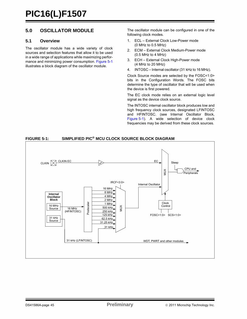
PIC16(L)F1507
5.0 OSCILLATOR MODULE
5.1 Overview
The oscillator module has a wide variety of clocksources and selection features that allow it to be usedin a wide range of applications while maximizing perfor-mance and minimizing power consumption. Figure 5-1illustrates a block diagram of the oscillator module.
The oscillator module can be configured in one of thefollowing clock modes.
1. ECL – External Clock Low-Power mode(0 MHz to 0.5 MHz)
2. ECM – External Clock Medium-Power mode(0.5 MHz to 4 MHz)
3. ECH – External Clock High-Power mode(4 MHz to 20 MHz)
4. INTOSC – Internal oscillator (31 kHz to 16 MHz).
Clock Source modes are selected by the FOSC<1:0>bits in the Configuration Words. The FOSC bitsdetermine the type of oscillator that will be used whenthe device is first powered.
The EC clock mode relies on an external logic levelsignal as the device clock source.
The INTOSC internal oscillator block produces low andhigh frequency clock sources, designated LFINTOSCand HFINTOSC. (see Internal Oscillator Block,Figure 5-1). A wide selection of device clockfrequencies may be derived from these clock sources.
FIGURE 5-1: SIMPLIFIED PIC® MCU CLOCK SOURCE BLOCK DIAGRAM
FOSC<1:0>
EC
CPU and
Po
stsc
ale
r
MU
X
MU
X
16 MHz8 MHz4 MHz2 MHz1 MHz
250 kHz500 kHz
IRCF<3:0>
31 kHz
16 MHzSource
InternalOscillator
Block
WDT, PWRT and other modules
16 MHz
Internal Oscillator
(HFINTOSC)
ClockControl
SCS<1:0>
31 kHz (LFINTOSC)
31 kHzSource
125 kHz
31.25 kHz62.5 kHz
Peripherals
SleepCLKINCLKIN EC
DS41586A-page 45 Preliminary 2011 Microchip Technology Inc.
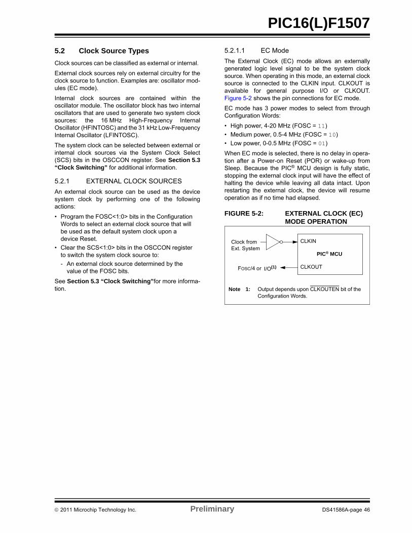
PIC16(L)F1507
5.2 Clock Source Types
Clock sources can be classified as external or internal.
External clock sources rely on external circuitry for theclock source to function. Examples are: oscillator mod-ules (EC mode).
Internal clock sources are contained within theoscillator module. The oscillator block has two internaloscillators that are used to generate two system clocksources: the 16 MHz High-Frequency InternalOscillator (HFINTOSC) and the 31 kHz Low-FrequencyInternal Oscillator (LFINTOSC).
The system clock can be selected between external orinternal clock sources via the System Clock Select(SCS) bits in the OSCCON register. See Section 5.3“Clock Switching” for additional information.
5.2.1 EXTERNAL CLOCK SOURCES
An external clock source can be used as the devicesystem clock by performing one of the followingactions:
• Program the FOSC<1:0> bits in the Configuration Words to select an external clock source that will be used as the default system clock upon a device Reset.
• Clear the SCS<1:0> bits in the OSCCON register to switch the system clock source to:
- An external clock source determined by the value of the FOSC bits.
See Section 5.3 “Clock Switching”for more informa-tion.
5.2.1.1 EC Mode
The External Clock (EC) mode allows an externallygenerated logic level signal to be the system clocksource. When operating in this mode, an external clocksource is connected to the CLKIN input. CLKOUT isavailable for general purpose I/O or CLKOUT.Figure 5-2 shows the pin connections for EC mode.
EC mode has 3 power modes to select from throughConfiguration Words:
• High power, 4-20 MHz (FOSC = 11)
• Medium power, 0.5-4 MHz (FOSC = 10)
• Low power, 0-0.5 MHz (FOSC = 01)
When EC mode is selected, there is no delay in opera-tion after a Power-on Reset (POR) or wake-up fromSleep. Because the PIC® MCU design is fully static,stopping the external clock input will have the effect ofhalting the device while leaving all data intact. Uponrestarting the external clock, the device will resumeoperation as if no time had elapsed.
FIGURE 5-2: EXTERNAL CLOCK (EC) MODE OPERATION
CLKIN
CLKOUT
Clock fromExt. System
PIC® MCU
FOSC/4 or I/O(1)
Note 1: Output depends upon CLKOUTEN bit of the Configuration Words.
2011 Microchip Technology Inc. Preliminary DS41586A-page 46
PIC16(L)F1507
5.2.2 INTERNAL CLOCK SOURCES
The device may be configured to use the internal oscil-lator block as the system clock by performing one of thefollowing actions:
• Program the FOSC<1:0> bits in Configuration Words to select the INTOSC clock source, which will be used as the default system clock upon a device Reset.
• Write the SCS<1:0> bits in the OSCCON register to switch the system clock source to the internal oscillator during run-time. See Section 5.3 “Clock Switching”for more information.
In INTOSC mode, CLKIN is available for generalpurpose I/O. CLKOUT is available for general purposeI/O or CLKOUT.
The function of the CLKOUT pin is determined by theCLKOUTEN bit in Configuration Words.
The internal oscillator block has two independentoscillators clock sources.
1. The HFINTOSC (High-Frequency InternalOscillator) is factory calibrated and operates at16 MHz.
2. The LFINTOSC (Low-Frequency InternalOscillator) is uncalibrated and operates at31 kHz.
5.2.2.1 HFINTOSC
The High-Frequency Internal Oscillator (HFINTOSC) isa factory calibrated 16 MHz internal clock source.
The outputs of the HFINTOSC connects to a prescalerand multiplexer (see Figure 5-1). One of multiplefrequencies derived from the HFINTOSC can beselected via software using the IRCF<3:0> bits of theOSCCON register. See Section 5.2.2.4 “InternalOscillator Clock Switch Timing” for more information.
The HFINTOSC is enabled by:
• Configure the IRCF<3:0> bits of the OSCCON register for the desired HF frequency, and
• FOSC<1:0> = 00, or
• Set the System Clock Source (SCS) bits of the OSCCON register to ‘1x’.
A fast start-up oscillator allows internal circuits to powerup and stabilize before switching to HFINTOSC.
The High-Frequency Internal Oscillator Ready bit(HFIOFR) of the OSCSTAT register indicates when theHFINTOSC is running.
The High-Frequency Internal Oscillator Stable bit(HFIOFS) of the OSCSTAT register indicates when theHFINTOSC is running within 0.5% of its final value.
5.2.2.2 LFINTOSC
The Low-Frequency Internal Oscillator (LFINTOSC) isan uncalibrated 31 kHz internal clock source.
The output of the LFINTOSC connects to a multiplexer(see Figure 5-1). Select 31 kHz, via software, using theIRCF<3:0> bits of the OSCCON register. SeeSection 5.2.2.4 “Internal Oscillator Clock SwitchTiming” for more information. The LFINTOSC is alsothe frequency for the Power-up Timer (PWRT) andWatchdog Timer (WDT).
The LFINTOSC is enabled by selecting 31 kHz(IRCF<3:0> bits of the OSCCON register = 000x) asthe system clock source (SCS bits of the OSCCONregister = 1x), or when any of the following areenabled:
• Configure the IRCF<3:0> bits of the OSCCON register for the desired LF frequency, and
• FOSC<1:0> = 00, or
• Set the System Clock Source (SCS) bits of the OSCCON register to ‘1x’
Peripherals that use the LFINTOSC are:
• Power-up Timer (PWRT)
• Watchdog Timer (WDT)
The Low-Frequency Internal Oscillator Ready bit(LFIOFR) of the OSCSTAT register indicates when theLFINTOSC is running.
DS41586A-page 47 Preliminary 2011 Microchip Technology Inc.
PIC16(L)F1507
5.2.2.3 Internal Oscillator Frequency Selection
The system clock speed can be selected via softwareusing the Internal Oscillator Frequency Select bitsIRCF<3:0> of the OSCCON register.
The outputs of the 16 MHz HFINTOSC postscaler andthe LFINTOSC connect to a multiplexer (seeFigure 5-1). The Internal Oscillator Frequency Selectbits IRCF<3:0> of the OSCCON register select thefrequency output of the internal oscillators. One of thefollowing frequencies can be selected via software:
• HFINTOSC
- 16 MHz
- 8 MHz
- 4 MHz
- 2 MHz
- 1 MHz
- 500 kHz (Default after Reset)
- 250 kHz
- 125 kHz
- 62.5 kHz
- 31.25 kHz
• LFINTOSC
- 31 kHz
The IRCF<3:0> bits of the OSCCON register allowduplicate selections for some frequencies. These dupli-cate choices can offer system design trade-offs. Lowerpower consumption can be obtained when changingoscillator sources for a given frequency. Faster transi-tion times can be obtained between frequency changesthat use the same oscillator source.
5.2.2.4 Internal Oscillator Clock Switch Timing
When switching between the HFINTOSC and theLFINTOSC, the new oscillator may already be shutdown to save power (see Figure 5-3). If this is the case,there is a delay after the IRCF<3:0> bits of theOSCCON register are modified before the frequencyselection takes place. The OSCSTAT register willreflect the current active status of the HFINTOSC andLFINTOSC oscillators. The sequence of a frequencyselection is as follows:
1. IRCF<3:0> bits of the OSCCON register aremodified.
2. If the new clock is shut down, a clock start-updelay is started.
3. Clock switch circuitry waits for a falling edge ofthe current clock.
4. Clock switch is complete.
See Figure 5-3 for more details.
If the internal oscillator speed is switched between twoclocks of the same source, there is no start-up delaybefore the new frequency is selected.
Start-up delay specifications are located in theoscillator tables of Section 25.0 “ElectricalSpecifications”
Note: Following any Reset, the IRCF<3:0> bitsof the OSCCON register are set to ‘0111’and the frequency selection is set to500 kHz. The user can modify the IRCFbits to select a different frequency.
2011 Microchip Technology Inc. Preliminary DS41586A-page 48
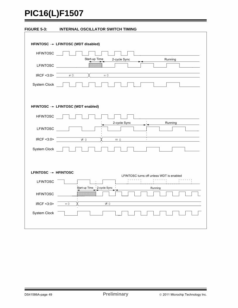
PIC16(L)F1507
FIGURE 5-3: INTERNAL OSCILLATOR SWITCH TIMING
HFINTOSC
LFINTOSC
IRCF <3:0>
System Clock
HFINTOSC
LFINTOSC
IRCF <3:0>
System Clock
0 0
0 0
Start-up Time 2-cycle Sync Running
2-cycle Sync Running
HFINTOSC LFINTOSC (WDT disabled)
HFINTOSC LFINTOSC (WDT enabled)
LFINTOSC
HFINTOSC
IRCF <3:0>
System Clock
= 0 0
Start-up Time 2-cycle Sync Running
LFINTOSC HFINTOSCLFINTOSC turns off unless WDT is enabled
DS41586A-page 49 Preliminary 2011 Microchip Technology Inc.
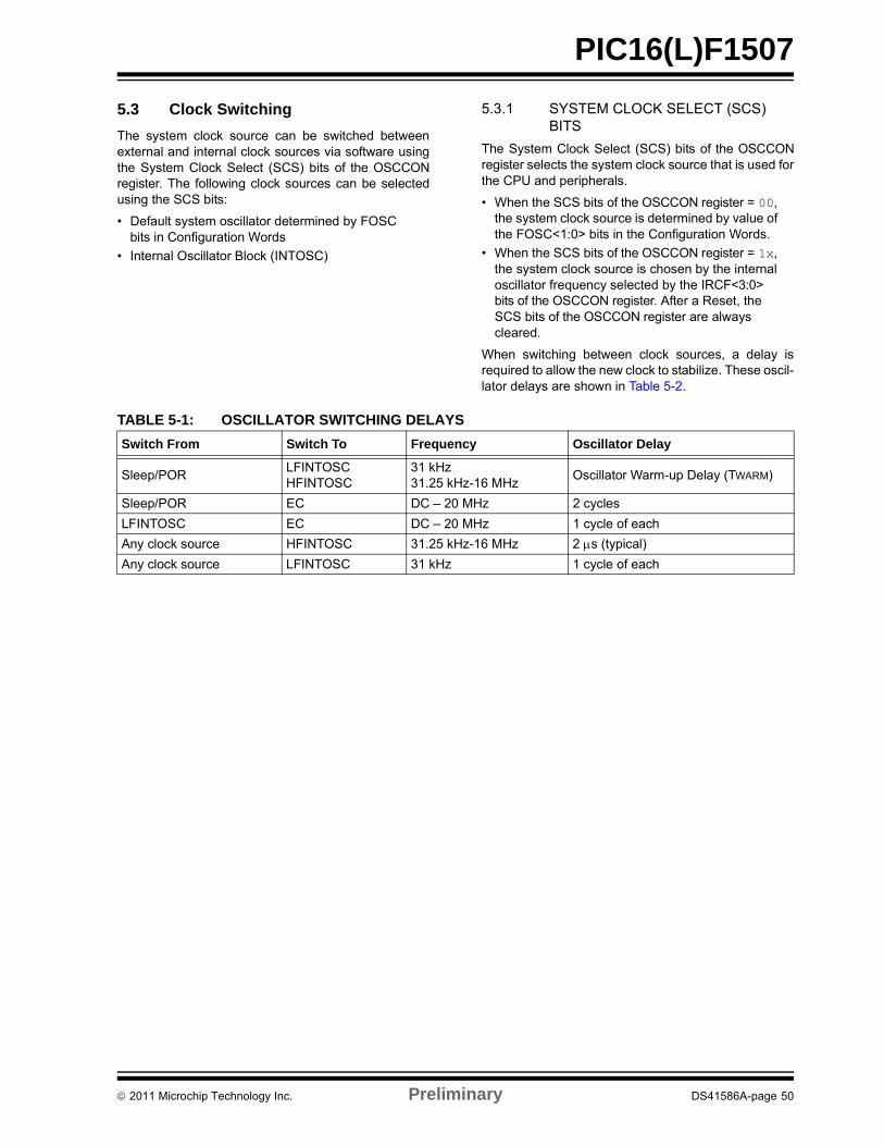
PIC16(L)F1507
5.3 Clock Switching
The system clock source can be switched betweenexternal and internal clock sources via software usingthe System Clock Select (SCS) bits of the OSCCONregister. The following clock sources can be selectedusing the SCS bits:
• Default system oscillator determined by FOSC bits in Configuration Words
• Internal Oscillator Block (INTOSC)
5.3.1 SYSTEM CLOCK SELECT (SCS) BITS
The System Clock Select (SCS) bits of the OSCCONregister selects the system clock source that is used forthe CPU and peripherals.
• When the SCS bits of the OSCCON register = 00, the system clock source is determined by value of the FOSC<1:0> bits in the Configuration Words.
• When the SCS bits of the OSCCON register = 1x, the system clock source is chosen by the internal oscillator frequency selected by the IRCF<3:0> bits of the OSCCON register. After a Reset, the SCS bits of the OSCCON register are always cleared.
When switching between clock sources, a delay isrequired to allow the new clock to stabilize. These oscil-lator delays are shown in Table 5-2.
TABLE 5-1: OSCILLATOR SWITCHING DELAYS
Switch From Switch To Frequency Oscillator Delay
Sleep/PORLFINTOSCHFINTOSC
31 kHz31.25 kHz-16 MHz
Oscillator Warm-up Delay (TWARM)
Sleep/POR EC DC – 20 MHz 2 cycles
LFINTOSC EC DC – 20 MHz 1 cycle of each
Any clock source HFINTOSC 31.25 kHz-16 MHz 2 s (typical)
Any clock source LFINTOSC 31 kHz 1 cycle of each
2011 Microchip Technology Inc. Preliminary DS41586A-page 50
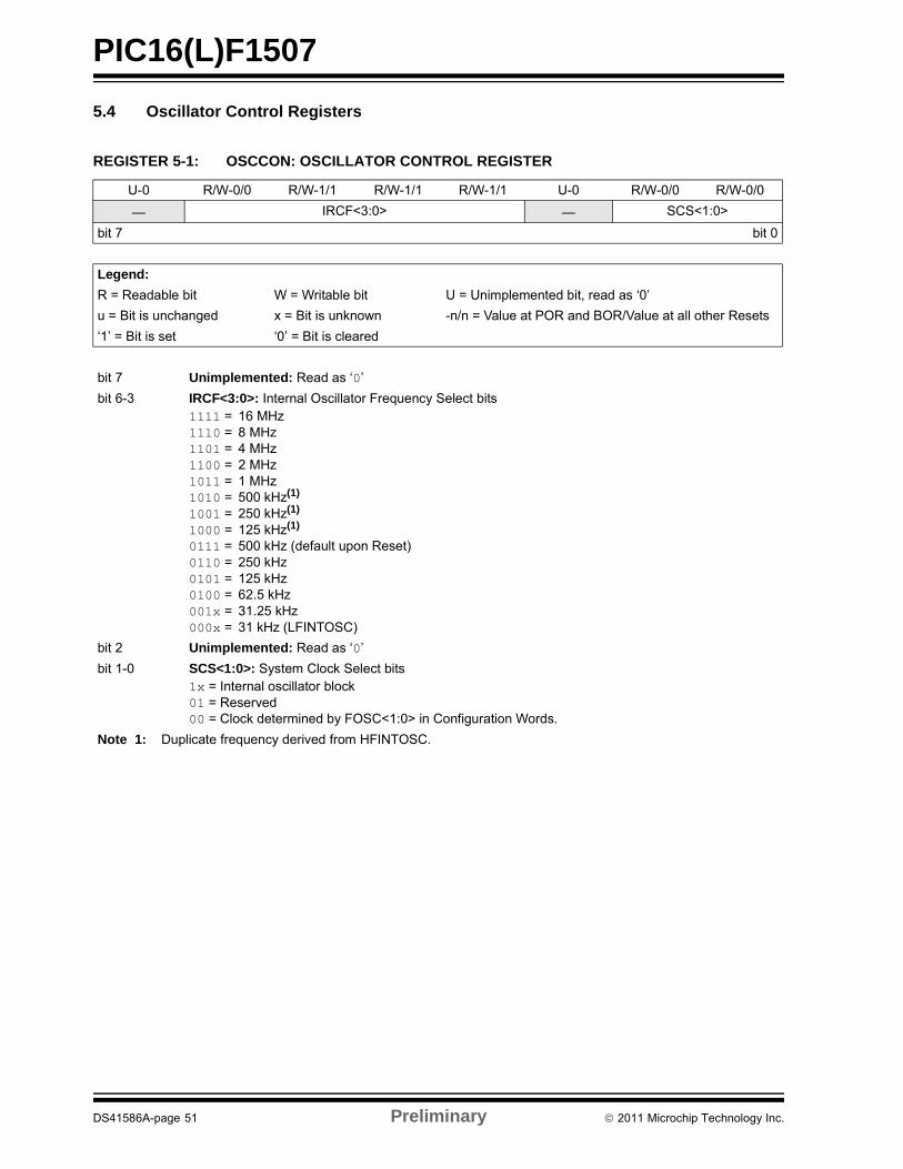
PIC16(L)F1507
5.4 Oscillator Control Registers
REGISTER 5-1: OSCCON: OSCILLATOR CONTROL REGISTER
U-0 R/W-0/0 R/W-1/1 R/W-1/1 R/W-1/1 U-0 R/W-0/0 R/W-0/0
— IRCF<3:0> — SCS<1:0>
bit 7 bit 0
Legend:
R = Readable bit W = Writable bit U = Unimplemented bit, read as ‘0’
u = Bit is unchanged x = Bit is unknown -n/n = Value at POR and BOR/Value at all other Resets
‘1’ = Bit is set ‘0’ = Bit is cleared
bit 7 Unimplemented: Read as ‘0’
bit 6-3 IRCF<3:0>: Internal Oscillator Frequency Select bits1111 = 16 MHz1110 = 8 MHz1101 = 4 MHz1100 = 2 MHz1011 = 1 MHz1010 = 500 kHz(1)
1001 = 250 kHz(1)
1000 = 125 kHz(1)
0111 = 500 kHz (default upon Reset)0110 = 250 kHz0101 = 125 kHz0100 = 62.5 kHz001x = 31.25 kHz000x = 31 kHz (LFINTOSC)
bit 2 Unimplemented: Read as ‘0’
bit 1-0 SCS<1:0>: System Clock Select bits1x = Internal oscillator block01 = Reserved00 = Clock determined by FOSC<1:0> in Configuration Words.
Note 1: Duplicate frequency derived from HFINTOSC.
DS41586A-page 51 Preliminary 2011 Microchip Technology Inc.
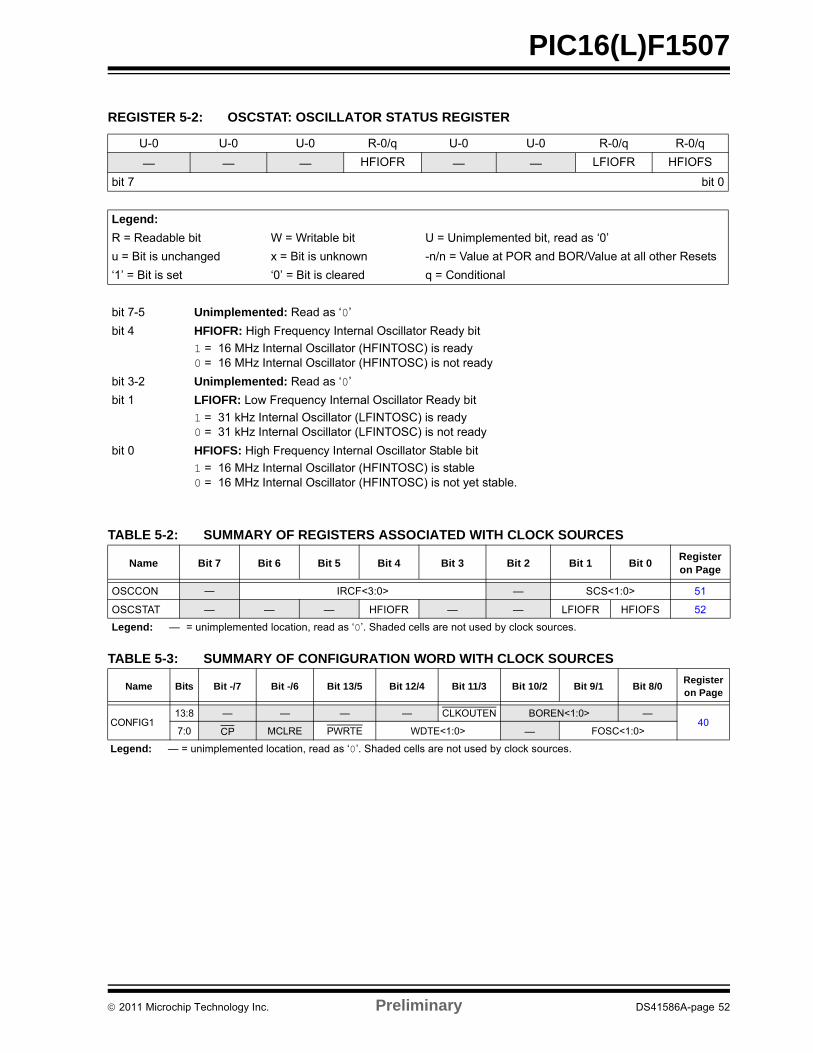
PIC16(L)F1507
TABLE 5-2: SUMMARY OF REGISTERS ASSOCIATED WITH CLOCK SOURCES
TABLE 5-3: SUMMARY OF CONFIGURATION WORD WITH CLOCK SOURCES
REGISTER 5-2: OSCSTAT: OSCILLATOR STATUS REGISTER
U-0 U-0 U-0 R-0/q U-0 U-0 R-0/q R-0/q
— — — HFIOFR — — LFIOFR HFIOFS
bit 7 bit 0
Legend:
R = Readable bit W = Writable bit U = Unimplemented bit, read as ‘0’
u = Bit is unchanged x = Bit is unknown -n/n = Value at POR and BOR/Value at all other Resets
‘1’ = Bit is set ‘0’ = Bit is cleared q = Conditional
bit 7-5 Unimplemented: Read as ‘0’
bit 4 HFIOFR: High Frequency Internal Oscillator Ready bit
1 = 16 MHz Internal Oscillator (HFINTOSC) is ready0 = 16 MHz Internal Oscillator (HFINTOSC) is not ready
bit 3-2 Unimplemented: Read as ‘0’
bit 1 LFIOFR: Low Frequency Internal Oscillator Ready bit
1 = 31 kHz Internal Oscillator (LFINTOSC) is ready0 = 31 kHz Internal Oscillator (LFINTOSC) is not ready
bit 0 HFIOFS: High Frequency Internal Oscillator Stable bit
1 = 16 MHz Internal Oscillator (HFINTOSC) is stable0 = 16 MHz Internal Oscillator (HFINTOSC) is not yet stable.
Name Bit 7 Bit 6 Bit 5 Bit 4 Bit 3 Bit 2 Bit 1 Bit 0Register on Page
OSCCON — IRCF<3:0> — SCS<1:0> 51
OSCSTAT — — — HFIOFR — — LFIOFR HFIOFS 52
Legend: — = unimplemented location, read as ‘0’. Shaded cells are not used by clock sources.
Name Bits Bit -/7 Bit -/6 Bit 13/5 Bit 12/4 Bit 11/3 Bit 10/2 Bit 9/1 Bit 8/0Register on Page
CONFIG113:8 — — — — CLKOUTEN BOREN<1:0> —
407:0 CP MCLRE PWRTE WDTE<1:0> — FOSC<1:0>
Legend: — = unimplemented location, read as ‘0’. Shaded cells are not used by clock sources.
2011 Microchip Technology Inc. Preliminary DS41586A-page 52
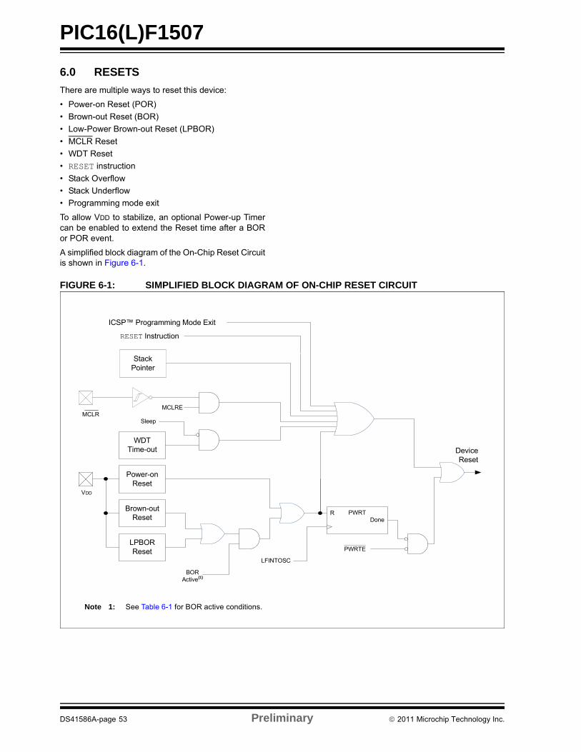
PIC16(L)F1507
6.0 RESETS
There are multiple ways to reset this device:
• Power-on Reset (POR)
• Brown-out Reset (BOR)
• Low-Power Brown-out Reset (LPBOR)
• MCLR Reset
• WDT Reset
• RESET instruction
• Stack Overflow
• Stack Underflow
• Programming mode exit
To allow VDD to stabilize, an optional Power-up Timercan be enabled to extend the Reset time after a BORor POR event.
A simplified block diagram of the On-Chip Reset Circuitis shown in Figure 6-1.
FIGURE 6-1: SIMPLIFIED BLOCK DIAGRAM OF ON-CHIP RESET CIRCUIT
Note 1: See Table 6-1 for BOR active conditions.
DeviceReset
Power-on Reset
WDT Time-out
Brown-out Reset
LPBOR Reset
RESET Instruction
MCLRE
Sleep
BOR Active(1)
PWRTRDone
PWRTE
LFINTOSC
VDD
ICSP™ Programming Mode Exit
Stack Pointer
MCLR
DS41586A-page 53 Preliminary 2011 Microchip Technology Inc.
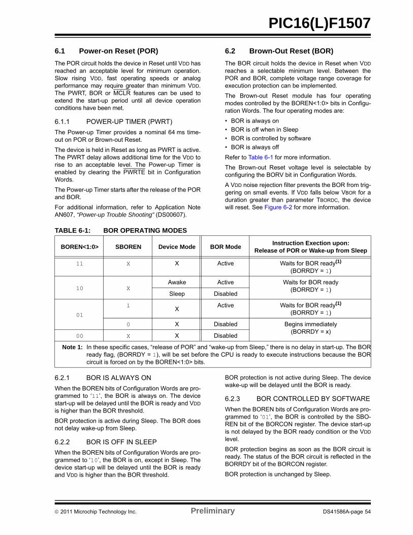
PIC16(L)F1507
6.1 Power-on Reset (POR)
The POR circuit holds the device in Reset until VDD hasreached an acceptable level for minimum operation.Slow rising VDD, fast operating speeds or analogperformance may require greater than minimum VDD.The PWRT, BOR or MCLR features can be used toextend the start-up period until all device operationconditions have been met.
6.1.1 POWER-UP TIMER (PWRT)
The Power-up Timer provides a nominal 64 ms time-out on POR or Brown-out Reset.
The device is held in Reset as long as PWRT is active.The PWRT delay allows additional time for the VDD torise to an acceptable level. The Power-up Timer isenabled by clearing the PWRTE bit in ConfigurationWords.
The Power-up Timer starts after the release of the PORand BOR.
For additional information, refer to Application NoteAN607, “Power-up Trouble Shooting” (DS00607).
6.2 Brown-Out Reset (BOR)
The BOR circuit holds the device in Reset when VDD
reaches a selectable minimum level. Between thePOR and BOR, complete voltage range coverage forexecution protection can be implemented.
The Brown-out Reset module has four operatingmodes controlled by the BOREN<1:0> bits in Configu-ration Words. The four operating modes are:
• BOR is always on
• BOR is off when in Sleep
• BOR is controlled by software
• BOR is always off
Refer to Table 6-1 for more information.
The Brown-out Reset voltage level is selectable byconfiguring the BORV bit in Configuration Words.
A VDD noise rejection filter prevents the BOR from trig-gering on small events. If VDD falls below VBOR for aduration greater than parameter TBORDC, the devicewill reset. See Figure 6-2 for more information.
TABLE 6-1: BOR OPERATING MODES
6.2.1 BOR IS ALWAYS ON
When the BOREN bits of Configuration Words are pro-grammed to ‘11’, the BOR is always on. The devicestart-up will be delayed until the BOR is ready and VDD
is higher than the BOR threshold.
BOR protection is active during Sleep. The BOR doesnot delay wake-up from Sleep.
6.2.2 BOR IS OFF IN SLEEP
When the BOREN bits of Configuration Words are pro-grammed to ‘10’, the BOR is on, except in Sleep. Thedevice start-up will be delayed until the BOR is readyand VDD is higher than the BOR threshold.
BOR protection is not active during Sleep. The devicewake-up will be delayed until the BOR is ready.
6.2.3 BOR CONTROLLED BY SOFTWARE
When the BOREN bits of Configuration Words are pro-grammed to ‘01’, the BOR is controlled by the SBO-REN bit of the BORCON register. The device start-upis not delayed by the BOR ready condition or the VDD
level.
BOR protection begins as soon as the BOR circuit isready. The status of the BOR circuit is reflected in theBORRDY bit of the BORCON register.
BOR protection is unchanged by Sleep.
BOREN<1:0> SBOREN Device Mode BOR ModeInstruction Exection upon:
Release of POR or Wake-up from Sleep
11 X X Active Waits for BOR ready(1)
(BORRDY = 1)
10 XAwake Active Waits for BOR ready
(BORRDY = 1)Sleep Disabled
01
1X
Active Waits for BOR ready(1)
(BORRDY = 1)
0 X Disabled Begins immediately(BORRDY = x)
00 X X Disabled
Note 1: In these specific cases, “release of POR” and “wake-up from Sleep,” there is no delay in start-up. The BORready flag, (BORRDY = 1), will be set before the CPU is ready to execute instructions because the BORcircuit is forced on by the BOREN<1:0> bits.
2011 Microchip Technology Inc. Preliminary DS41586A-page 54
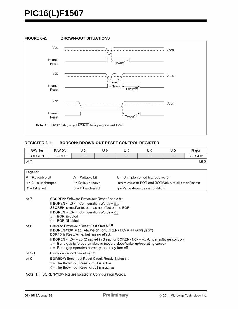
PIC16(L)F1507
FIGURE 6-2: BROWN-OUT SITUATIONS
REGISTER 6-1: BORCON: BROWN-OUT RESET CONTROL REGISTER
R/W-1/u R/W-0/u U-0 U-0 U-0 U-0 U-0 R-q/u
SBOREN BORFS — — — — — BORRDY
bit 7 bit 0
Legend:
R = Readable bit W = Writable bit U = Unimplemented bit, read as ‘0’
u = Bit is unchanged x = Bit is unknown -n/n = Value at POR and BOR/Value at all other Resets
‘1’ = Bit is set ‘0’ = Bit is cleared q = Value depends on condition
bit 7 SBOREN: Software Brown-out Reset Enable bitIf BOREN <1:0> in Configuration Words 01:SBOREN is read/write, but has no effect on the BOR.If BOREN <1:0> in Configuration Words = 01:1 = BOR Enabled0 = BOR Disabled
bit 6 BORFS: Brown-out Reset Fast Start bit(1)
If BOREN<1:0> = 11 (Always on) or BOREN<1:0> = 00 (Always off)BORFS is Read/Write, but has no effect.
If BOREN <1:0> = 10 (Disabled in Sleep) or BOREN<1:0> = 01 (Under software control):1 = Band gap is forced on always (covers sleep/wake-up/operating cases)0 = Band gap operates normally, and may turn off
bit 5-1 Unimplemented: Read as ‘0’
bit 0 BORRDY: Brown-out Reset Circuit Ready Status bit1 = The Brown-out Reset circuit is active0 = The Brown-out Reset circuit is inactive
Note 1: BOREN<1:0> bits are located in Configuration Words.
TPWRT(1)
VBOR VDD
InternalReset
VBOR VDD
InternalReset TPWRT(1)< TPWRT
TPWRT(1)
VBOR VDD
InternalReset
Note 1: TPWRT delay only if PWRTE bit is programmed to ‘0’.
DS41586A-page 55 Preliminary 2011 Microchip Technology Inc.
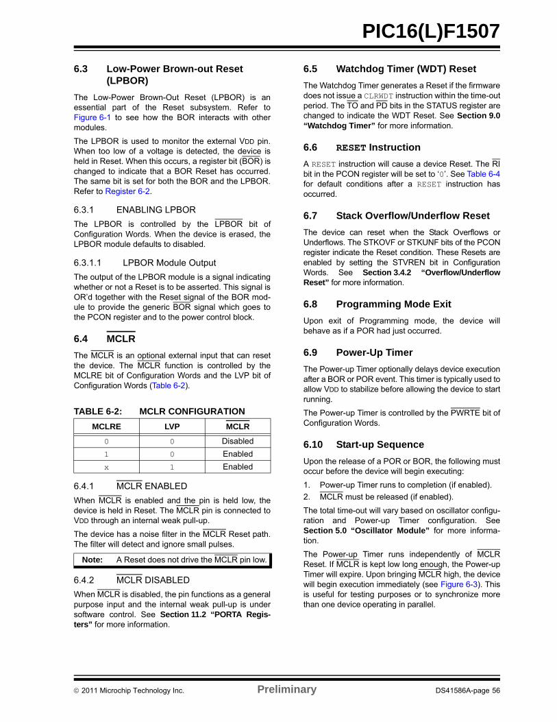
PIC16(L)F1507
6.3 Low-Power Brown-out Reset (LPBOR)
The Low-Power Brown-Out Reset (LPBOR) is anessential part of the Reset subsystem. Refer toFigure 6-1 to see how the BOR interacts with othermodules.
The LPBOR is used to monitor the external VDD pin.When too low of a voltage is detected, the device isheld in Reset. When this occurs, a register bit (BOR) ischanged to indicate that a BOR Reset has occurred.The same bit is set for both the BOR and the LPBOR.Refer to Register 6-2.
6.3.1 ENABLING LPBOR
The LPBOR is controlled by the LPBOR bit ofConfiguration Words. When the device is erased, theLPBOR module defaults to disabled.
6.3.1.1 LPBOR Module Output
The output of the LPBOR module is a signal indicatingwhether or not a Reset is to be asserted. This signal isOR’d together with the Reset signal of the BOR mod-ule to provide the generic BOR signal which goes tothe PCON register and to the power control block.
6.4 MCLR
The MCLR is an optional external input that can resetthe device. The MCLR function is controlled by theMCLRE bit of Configuration Words and the LVP bit ofConfiguration Words (Table 6-2).
6.4.1 MCLR ENABLED
When MCLR is enabled and the pin is held low, thedevice is held in Reset. The MCLR pin is connected toVDD through an internal weak pull-up.
The device has a noise filter in the MCLR Reset path.The filter will detect and ignore small pulses.
6.4.2 MCLR DISABLED
When MCLR is disabled, the pin functions as a generalpurpose input and the internal weak pull-up is undersoftware control. See Section 11.2 “PORTA Regis-ters” for more information.
6.5 Watchdog Timer (WDT) Reset
The Watchdog Timer generates a Reset if the firmwaredoes not issue a CLRWDT instruction within the time-outperiod. The TO and PD bits in the STATUS register arechanged to indicate the WDT Reset. See Section 9.0“Watchdog Timer” for more information.
6.6 RESET Instruction
A RESET instruction will cause a device Reset. The RIbit in the PCON register will be set to ‘0’. See Table 6-4for default conditions after a RESET instruction hasoccurred.
6.7 Stack Overflow/Underflow Reset
The device can reset when the Stack Overflows orUnderflows. The STKOVF or STKUNF bits of the PCONregister indicate the Reset condition. These Resets areenabled by setting the STVREN bit in ConfigurationWords. See Section 3.4.2 “Overflow/UnderflowReset” for more information.
6.8 Programming Mode Exit
Upon exit of Programming mode, the device willbehave as if a POR had just occurred.
6.9 Power-Up Timer
The Power-up Timer optionally delays device executionafter a BOR or POR event. This timer is typically used toallow VDD to stabilize before allowing the device to startrunning.
The Power-up Timer is controlled by the PWRTE bit ofConfiguration Words.
6.10 Start-up Sequence
Upon the release of a POR or BOR, the following mustoccur before the device will begin executing:
1. Power-up Timer runs to completion (if enabled).
2. MCLR must be released (if enabled).
The total time-out will vary based on oscillator configu-ration and Power-up Timer configuration. SeeSection 5.0 “Oscillator Module” for more informa-tion.
The Power-up Timer runs independently of MCLRReset. If MCLR is kept low long enough, the Power-upTimer will expire. Upon bringing MCLR high, the devicewill begin execution immediately (see Figure 6-3). Thisis useful for testing purposes or to synchronize morethan one device operating in parallel.
TABLE 6-2: MCLR CONFIGURATION
MCLRE LVP MCLR
0 0 Disabled
1 0 Enabled
x 1 Enabled
Note: A Reset does not drive the MCLR pin low.
2011 Microchip Technology Inc. Preliminary DS41586A-page 56
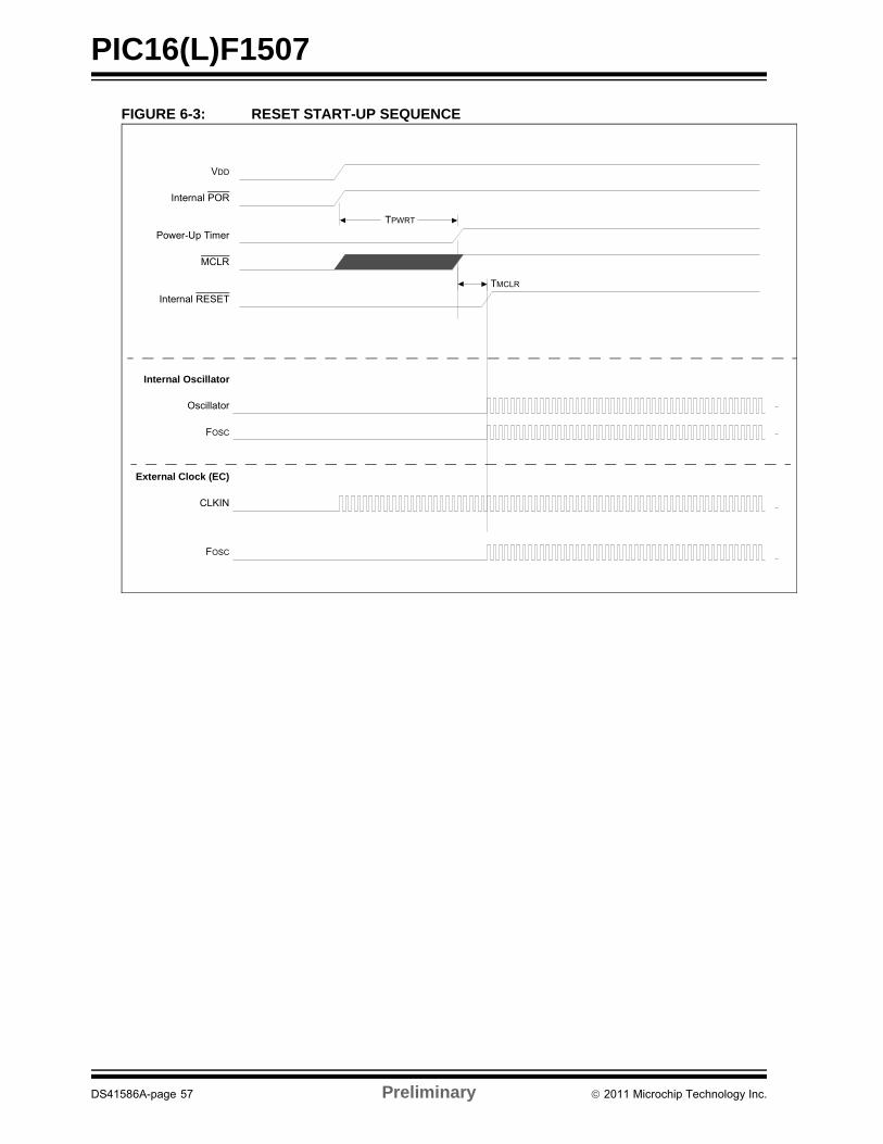
PIC16(L)F1507
DS4
FIGURE 6-3: RESET START-UP SEQUENCE
TMCLR
TPWRT
VDD
Internal POR
Power-Up Timer
MCLR
Internal RESET
Internal Oscillator
Oscillator
FOSC
External Clock (EC)
CLKIN
FOSC
1586A-page 57 Preliminary 2011 Microchip Technology Inc.
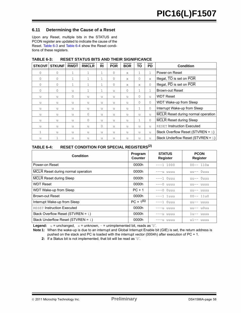
PIC16(L)F1507
6.11 Determining the Cause of a Reset
Upon any Reset, multiple bits in the STATUS andPCON register are updated to indicate the cause of theReset. Table 6-3 and Table 6-4 show the Reset condi-tions of these registers.
TABLE 6-3: RESET STATUS BITS AND THEIR SIGNIFICANCE
TABLE 6-4: RESET CONDITION FOR SPECIAL REGISTERS(2)
STKOVF STKUNF RWDT RMCLR RI POR BOR TO PD Condition
0 0 1 1 1 0 x 1 1 Power-on Reset
0 0 1 1 1 0 x 0 x Illegal, TO is set on POR
0 0 1 1 1 0 x x 0 Illegal, PD is set on POR
0 0 u 1 1 u 0 1 1 Brown-out Reset
u u 0 u u u u 0 u WDT Reset
u u u u u u u 0 0 WDT Wake-up from Sleep
u u u u u u u 1 0 Interrupt Wake-up from Sleep
u u u 0 u u u u u MCLR Reset during normal operation
u u u 0 u u u 1 0 MCLR Reset during Sleep
u u u u 0 u u u u RESET Instruction Executed
1 u u u u u u u u Stack Overflow Reset (STVREN = 1)
u 1 u u u u u u u Stack Underflow Reset (STVREN = 1)
ConditionProgramCounter
STATUSRegister
PCONRegister
Power-on Reset 0000h ---1 1000 00-- 110x
MCLR Reset during normal operation 0000h ---u uuuu uu-- 0uuu
MCLR Reset during Sleep 0000h ---1 0uuu uu-- 0uuu
WDT Reset 0000h ---0 uuuu uu-- uuuu
WDT Wake-up from Sleep PC + 1 ---0 0uuu uu-- uuuu
Brown-out Reset 0000h ---1 1uuu 00-- 11u0
Interrupt Wake-up from Sleep PC + 1(1) ---1 0uuu uu-- uuuu
RESET Instruction Executed 0000h ---u uuuu uu-- u0uu
Stack Overflow Reset (STVREN = 1) 0000h ---u uuuu 1u-- uuuu
Stack Underflow Reset (STVREN = 1) 0000h ---u uuuu u1-- uuuu
Legend: u = unchanged, x = unknown, - = unimplemented bit, reads as ‘0’.Note 1: When the wake-up is due to an interrupt and Global Interrupt Enable bit (GIE) is set, the return address is
pushed on the stack and PC is loaded with the interrupt vector (0004h) after execution of PC + 1.2: If a Status bit is not implemented, that bit will be read as ‘0’.
2011 Microchip Technology Inc. Preliminary DS41586A-page 58
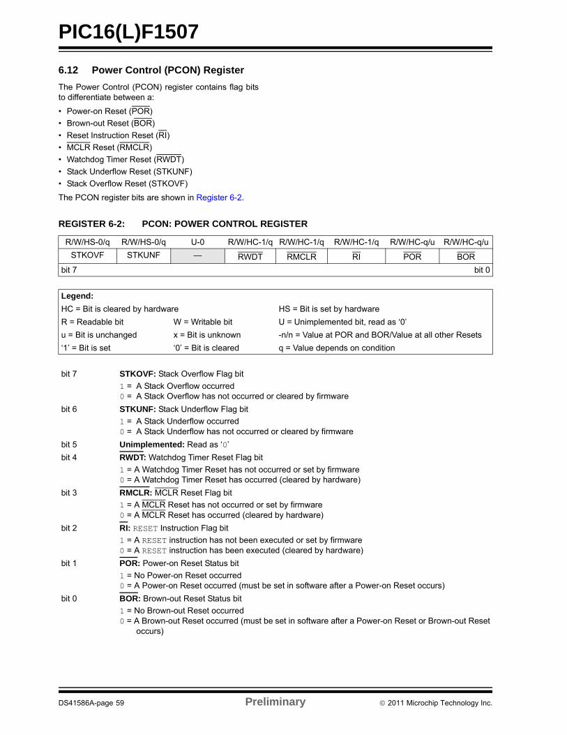
PIC16(L)F1507
6.12 Power Control (PCON) Register
The Power Control (PCON) register contains flag bitsto differentiate between a:
• Power-on Reset (POR)
• Brown-out Reset (BOR)
• Reset Instruction Reset (RI)
• MCLR Reset (RMCLR)
• Watchdog Timer Reset (RWDT)
• Stack Underflow Reset (STKUNF)
• Stack Overflow Reset (STKOVF)
The PCON register bits are shown in Register 6-2.
REGISTER 6-2: PCON: POWER CONTROL REGISTER
R/W/HS-0/q R/W/HS-0/q U-0 R/W/HC-1/q R/W/HC-1/q R/W/HC-1/q R/W/HC-q/u R/W/HC-q/u
STKOVF STKUNF — RWDT RMCLR RI POR BOR
bit 7 bit 0
Legend:
HC = Bit is cleared by hardware HS = Bit is set by hardware
R = Readable bit W = Writable bit U = Unimplemented bit, read as ‘0’
u = Bit is unchanged x = Bit is unknown -n/n = Value at POR and BOR/Value at all other Resets
‘1’ = Bit is set ‘0’ = Bit is cleared q = Value depends on condition
bit 7 STKOVF: Stack Overflow Flag bit
1 = A Stack Overflow occurred0 = A Stack Overflow has not occurred or cleared by firmware
bit 6 STKUNF: Stack Underflow Flag bit
1 = A Stack Underflow occurred0 = A Stack Underflow has not occurred or cleared by firmware
bit 5 Unimplemented: Read as ‘0’
bit 4 RWDT: Watchdog Timer Reset Flag bit
1 = A Watchdog Timer Reset has not occurred or set by firmware0 = A Watchdog Timer Reset has occurred (cleared by hardware)
bit 3 RMCLR: MCLR Reset Flag bit
1 = A MCLR Reset has not occurred or set by firmware0 = A MCLR Reset has occurred (cleared by hardware)
bit 2 RI: RESET Instruction Flag bit
1 = A RESET instruction has not been executed or set by firmware0 = A RESET instruction has been executed (cleared by hardware)
bit 1 POR: Power-on Reset Status bit
1 = No Power-on Reset occurred0 = A Power-on Reset occurred (must be set in software after a Power-on Reset occurs)
bit 0 BOR: Brown-out Reset Status bit
1 = No Brown-out Reset occurred0 = A Brown-out Reset occurred (must be set in software after a Power-on Reset or Brown-out Reset
occurs)
DS41586A-page 59 Preliminary 2011 Microchip Technology Inc.
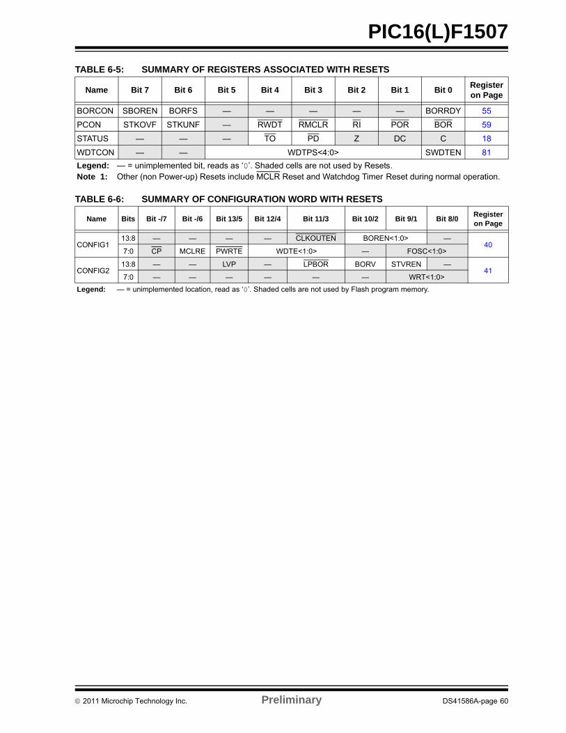
PIC16(L)F1507
TABLE 6-5: SUMMARY OF REGISTERS ASSOCIATED WITH RESETS
TABLE 6-6: SUMMARY OF CONFIGURATION WORD WITH RESETS
Name Bit 7 Bit 6 Bit 5 Bit 4 Bit 3 Bit 2 Bit 1 Bit 0Register on Page
BORCON SBOREN BORFS — — — — — BORRDY 55
PCON STKOVF STKUNF — RWDT RMCLR RI POR BOR 59
STATUS — — — TO PD Z DC C 18
WDTCON — — WDTPS<4:0> SWDTEN 81
Legend: — = unimplemented bit, reads as ‘0’. Shaded cells are not used by Resets.Note 1: Other (non Power-up) Resets include MCLR Reset and Watchdog Timer Reset during normal operation.
Name Bits Bit -/7 Bit -/6 Bit 13/5 Bit 12/4 Bit 11/3 Bit 10/2 Bit 9/1 Bit 8/0Register on Page
CONFIG113:8 — — — — CLKOUTEN BOREN<1:0> —
407:0 CP MCLRE PWRTE WDTE<1:0> — FOSC<1:0>
CONFIG213:8 — — LVP — LPBOR BORV STVREN —
417:0 — — — — — — WRT<1:0>
Legend: — = unimplemented location, read as ‘0’. Shaded cells are not used by Flash program memory.
2011 Microchip Technology Inc. Preliminary DS41586A-page 60
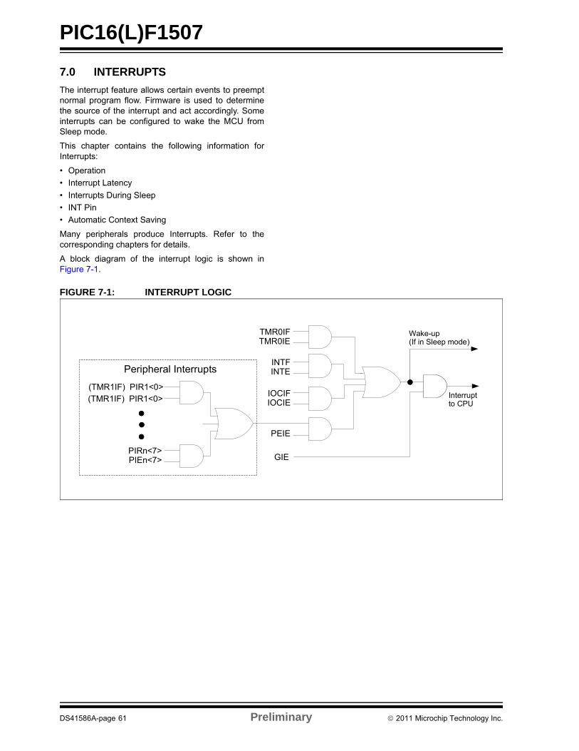
PIC16(L)F1507
7.0 INTERRUPTS
The interrupt feature allows certain events to preemptnormal program flow. Firmware is used to determinethe source of the interrupt and act accordingly. Someinterrupts can be configured to wake the MCU fromSleep mode.
This chapter contains the following information forInterrupts:
• Operation
• Interrupt Latency
• Interrupts During Sleep
• INT Pin
• Automatic Context Saving
Many peripherals produce Interrupts. Refer to thecorresponding chapters for details.
A block diagram of the interrupt logic is shown inFigure 7-1.
FIGURE 7-1: INTERRUPT LOGIC
TMR0IFTMR0IE
INTFINTE
IOCIFIOCIE
Interruptto CPU
Wake-up (If in Sleep mode)
GIE
(TMR1IF) PIR1<0>
PIRn<7>PIEn<7>
PEIE
Peripheral Interrupts
(TMR1IF) PIR1<0>
DS41586A-page 61 Preliminary 2011 Microchip Technology Inc.
PIC16(L)F1507
7.1 Operation
Interrupts are disabled upon any device Reset. Theyare enabled by setting the following bits:
• GIE bit of the INTCON register
• Interrupt Enable bit(s) for the specific interrupt event(s)
• PEIE bit of the INTCON register (if the Interrupt Enable bit of the interrupt event is contained in the PIE1, PIE2 and PIE3 registers)
The INTCON, PIR1, PIR2 and PIR3 registers recordindividual interrupts via interrupt flag bits. Interrupt flagbits will be set, regardless of the status of the GIE, PEIEand individual interrupt enable bits.
The following events happen when an interrupt eventoccurs while the GIE bit is set:
• Current prefetched instruction is flushed
• GIE bit is cleared
• Current Program Counter (PC) is pushed onto the stack
• Critical registers are automatically saved to the shadow registers (See “Section 7.5 “Automatic Context Saving”.”)
• PC is loaded with the interrupt vector 0004h
The firmware within the Interrupt Service Routine (ISR)should determine the source of the interrupt by pollingthe interrupt flag bits. The interrupt flag bits must becleared before exiting the ISR to avoid repeatedinterrupts. Because the GIE bit is cleared, any interruptthat occurs while executing the ISR will be recordedthrough its interrupt flag, but will not cause theprocessor to redirect to the interrupt vector.
The RETFIE instruction exits the ISR by popping theprevious address from the stack, restoring the savedcontext from the shadow registers and setting the GIEbit.
For additional information on a specific interrupt’soperation, refer to its peripheral chapter.
7.2 Interrupt Latency
Interrupt latency is defined as the time from when theinterrupt event occurs to the time code execution at theinterrupt vector begins. The latency for synchronousinterrupts is 3 or 4 instruction cycles. For asynchronousinterrupts, the latency is 3 to 5 instruction cycles,depending on when the interrupt occurs. See Figure 7-2and Figure 7.3 for more details.
Note 1: Individual interrupt flag bits are set,regardless of the state of any otherenable bits.
2: All interrupts will be ignored while the GIEbit is cleared. Any interrupt occurringwhile the GIE bit is clear will be servicedwhen the GIE bit is set again.
2011 Microchip Technology Inc. Preliminary DS41586A-page 62
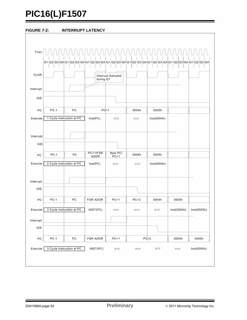
PIC16(L)F1507
FIGURE 7-2: INTERRUPT LATENCY
Q1 Q2 Q3 Q4 Q1 Q2 Q3 Q4 Q1 Q2 Q3 Q4 Q1 Q2 Q3 Q4 Q1 Q2 Q3 Q4 Q1 Q2 Q3 Q4
Fosc
CLKR
PC 0004h 0005hPC
Inst(0004h)NOP
GIE
Q1 Q2 Q3 Q4Q1 Q2 Q3 Q4
1 Cycle Instruction at PC
PC
Inst(0004h)NOP2 Cycle Instruction at PC
FSR ADDR PC+1 PC+2 0004h 0005hPC
Inst(0004h)NOP
GIE
PCPC-1
3 Cycle Instruction at PC
Execute
Interrupt
Inst(PC)
Interrupt Sampled during Q1
Inst(PC)
PC-1 PC+1
NOP
PCNew PC/
PC+10005hPC-1
PC+1/FSR ADDR
0004h
NOP
Interrupt
GIE
Interrupt
INST(PC) NOPNOP
FSR ADDR PC+1 PC+2 0004h 0005hPC
Inst(0004h)NOP
GIE
PCPC-1
3 Cycle Instruction at PC
Interrupt
INST(PC) NOPNOP NOP
Inst(0005h)
Execute
Execute
Execute
DS41586A-page 63 Preliminary 2011 Microchip Technology Inc.
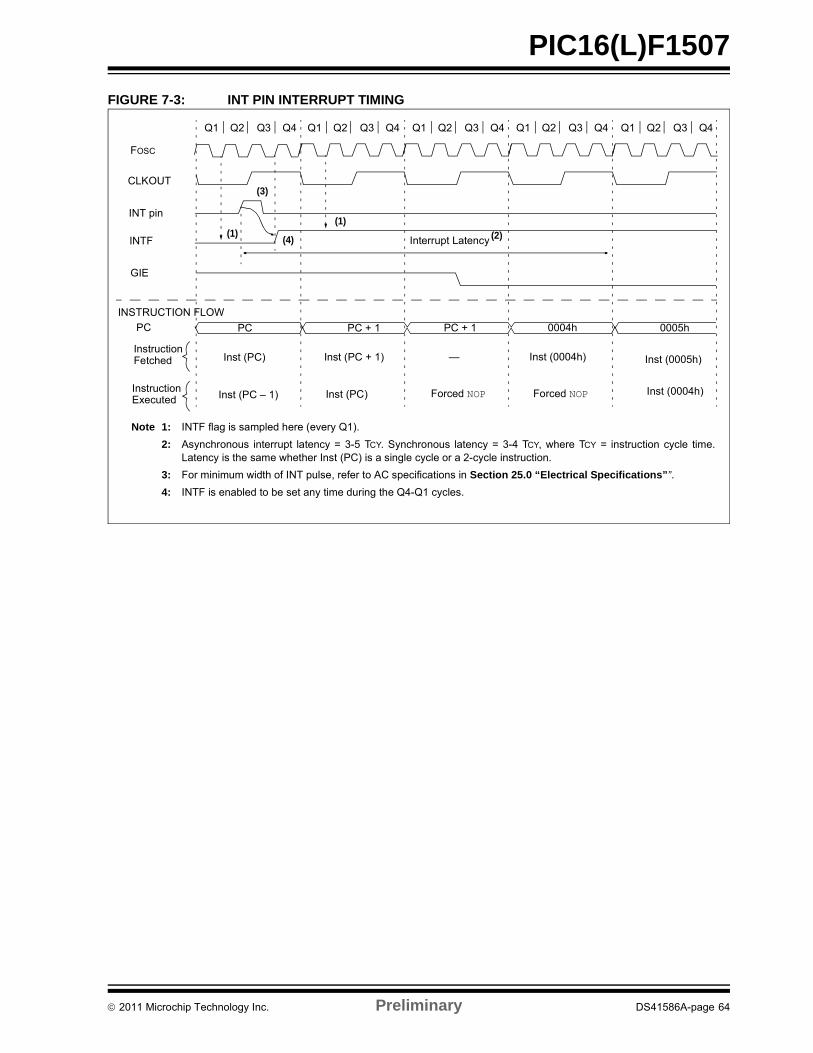
PIC16(L)F1507
FIGURE 7-3: INT PIN INTERRUPT TIMING
Q2Q1 Q3 Q4 Q2Q1 Q3 Q4 Q2Q1 Q3 Q4 Q2Q1 Q3 Q4 Q2Q1 Q3 Q4
FOSC
CLKOUT
INT pin
INTF
GIE
INSTRUCTION FLOW
PC
InstructionFetched
InstructionExecuted
Interrupt Latency
PC PC + 1 PC + 1 0004h 0005h
Inst (0004h) Inst (0005h)
Forced NOP
Inst (PC) Inst (PC + 1)
Inst (PC – 1) Inst (0004h) Forced NOPInst (PC)
—
Note 1: INTF flag is sampled here (every Q1).
2: Asynchronous interrupt latency = 3-5 TCY. Synchronous latency = 3-4 TCY, where TCY = instruction cycle time.Latency is the same whether Inst (PC) is a single cycle or a 2-cycle instruction.
3: For minimum width of INT pulse, refer to AC specifications in Section 25.0 “Electrical Specifications””.
4: INTF is enabled to be set any time during the Q4-Q1 cycles.
(1)
(2)
(3)
(4)(1)
2011 Microchip Technology Inc. Preliminary DS41586A-page 64
PIC16(L)F1507
7.3 Interrupts During Sleep
Some interrupts can be used to wake from Sleep. Towake from Sleep, the peripheral must be able tooperate without the system clock. The interrupt sourcemust have the appropriate Interrupt Enable bit(s) setprior to entering Sleep.
On waking from Sleep, if the GIE bit is also set, theprocessor will branch to the interrupt vector. Otherwise,the processor will continue executing instructions afterthe SLEEP instruction. The instruction directly after theSLEEP instruction will always be executed beforebranching to the ISR. Refer to Section 8.0 “Power-Down Mode (Sleep)” for more details.
7.4 INT Pin
The INT pin can be used to generate an asynchronousedge-triggered interrupt. This interrupt is enabled bysetting the INTE bit of the INTCON register. TheINTEDG bit of the OPTION_REG register determines onwhich edge the interrupt will occur. When the INTEDGbit is set, the rising edge will cause the interrupt. Whenthe INTEDG bit is clear, the falling edge will cause theinterrupt. The INTF bit of the INTCON register will be setwhen a valid edge appears on the INT pin. If the GIE andINTE bits are also set, the processor will redirectprogram execution to the interrupt vector.
7.5 Automatic Context Saving
Upon entering an interrupt, the return PC address issaved on the stack. Additionally, the following registersare automatically saved in the Shadow registers:
• W register
• STATUS register (except for TO and PD)
• BSR register
• FSR registers
• PCLATH register
Upon exiting the Interrupt Service Routine, these regis-ters are automatically restored. Any modifications tothese registers during the ISR will be lost. If modifica-tions to any of these registers are desired, the corre-sponding Shadow register should be modified and thevalue will be restored when exiting the ISR. TheShadow registers are available in Bank 31 and arereadable and writable. Depending on the user’s appli-cation, other registers may also need to be saved.
DS41586A-page 65 Preliminary 2011 Microchip Technology Inc.
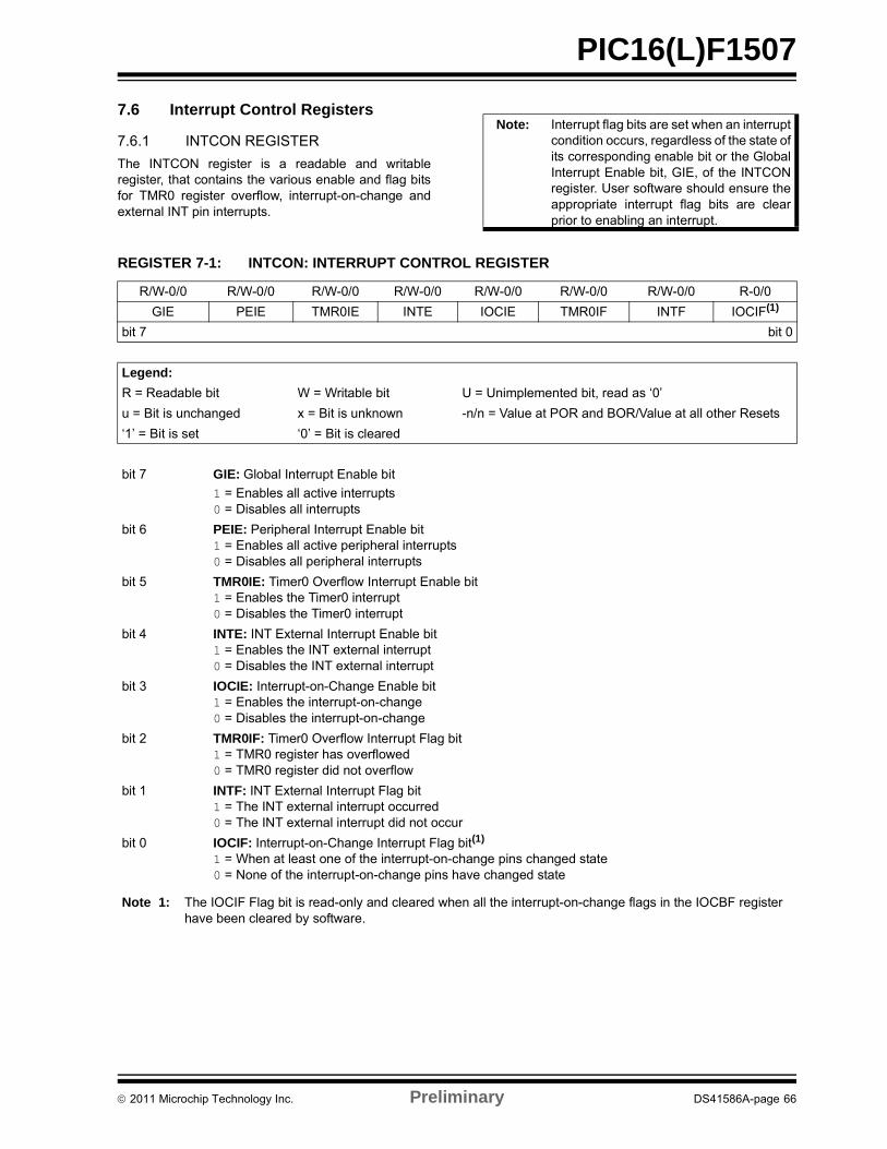
PIC16(L)F1507
7.6 Interrupt Control Registers
7.6.1 INTCON REGISTER
The INTCON register is a readable and writableregister, that contains the various enable and flag bitsfor TMR0 register overflow, interrupt-on-change andexternal INT pin interrupts.
Note: Interrupt flag bits are set when an interruptcondition occurs, regardless of the state ofits corresponding enable bit or the GlobalInterrupt Enable bit, GIE, of the INTCONregister. User software should ensure theappropriate interrupt flag bits are clearprior to enabling an interrupt.
REGISTER 7-1: INTCON: INTERRUPT CONTROL REGISTER
R/W-0/0 R/W-0/0 R/W-0/0 R/W-0/0 R/W-0/0 R/W-0/0 R/W-0/0 R-0/0
GIE PEIE TMR0IE INTE IOCIE TMR0IF INTF IOCIF(1)
bit 7 bit 0
Legend:
R = Readable bit W = Writable bit U = Unimplemented bit, read as ‘0’
u = Bit is unchanged x = Bit is unknown -n/n = Value at POR and BOR/Value at all other Resets
‘1’ = Bit is set ‘0’ = Bit is cleared
bit 7 GIE: Global Interrupt Enable bit
1 = Enables all active interrupts0 = Disables all interrupts
bit 6 PEIE: Peripheral Interrupt Enable bit1 = Enables all active peripheral interrupts0 = Disables all peripheral interrupts
bit 5 TMR0IE: Timer0 Overflow Interrupt Enable bit1 = Enables the Timer0 interrupt0 = Disables the Timer0 interrupt
bit 4 INTE: INT External Interrupt Enable bit1 = Enables the INT external interrupt0 = Disables the INT external interrupt
bit 3 IOCIE: Interrupt-on-Change Enable bit1 = Enables the interrupt-on-change0 = Disables the interrupt-on-change
bit 2 TMR0IF: Timer0 Overflow Interrupt Flag bit1 = TMR0 register has overflowed0 = TMR0 register did not overflow
bit 1 INTF: INT External Interrupt Flag bit1 = The INT external interrupt occurred0 = The INT external interrupt did not occur
bit 0 IOCIF: Interrupt-on-Change Interrupt Flag bit(1)
1 = When at least one of the interrupt-on-change pins changed state0 = None of the interrupt-on-change pins have changed state
Note 1: The IOCIF Flag bit is read-only and cleared when all the interrupt-on-change flags in the IOCBF register have been cleared by software.
2011 Microchip Technology Inc. Preliminary DS41586A-page 66
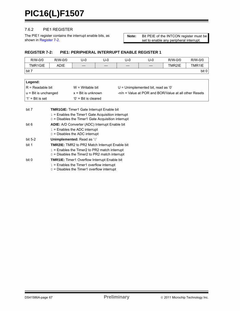
PIC16(L)F1507
7.6.2 PIE1 REGISTER
The PIE1 register contains the interrupt enable bits, asshown in Register 7-2.
Note: Bit PEIE of the INTCON register must beset to enable any peripheral interrupt.
REGISTER 7-2: PIE1: PERIPHERAL INTERRUPT ENABLE REGISTER 1
R/W-0/0 R/W-0/0 U-0 U-0 U-0 U-0 R/W-0/0 R/W-0/0
TMR1GIE ADIE — — — — TMR2IE TMR1IE
bit 7 bit 0
Legend:
R = Readable bit W = Writable bit U = Unimplemented bit, read as ‘0’
u = Bit is unchanged x = Bit is unknown -n/n = Value at POR and BOR/Value at all other Resets
‘1’ = Bit is set ‘0’ = Bit is cleared
bit 7 TMR1GIE: Timer1 Gate Interrupt Enable bit
1 = Enables the Timer1 Gate Acquisition interrupt0 = Disables the Timer1 Gate Acquisition interrupt
bit 6 ADIE: A/D Converter (ADC) Interrupt Enable bit
1 = Enables the ADC interrupt0 = Disables the ADC interrupt
bit 5-2 Unimplemented: Read as ‘0’
bit 1 TMR2IE: TMR2 to PR2 Match Interrupt Enable bit
1 = Enables the Timer2 to PR2 match interrupt0 = Disables the Timer2 to PR2 match interrupt
bit 0 TMR1IE: Timer1 Overflow Interrupt Enable bit
1 = Enables the Timer1 overflow interrupt0 = Disables the Timer1 overflow interrupt
DS41586A-page 67 Preliminary 2011 Microchip Technology Inc.
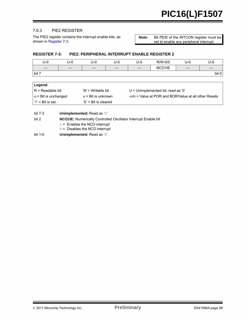
PIC16(L)F1507
7.6.3 PIE2 REGISTER
The PIE2 register contains the interrupt enable bits, asshown in Register 7-3.
Note: Bit PEIE of the INTCON register must beset to enable any peripheral interrupt.
REGISTER 7-3: PIE2: PERIPHERAL INTERRUPT ENABLE REGISTER 2
U-0 U-0 U-0 U-0 U-0 R/W-0/0 U-0 U-0
— — — — — NCO1IE — —
bit 7 bit 0
Legend:
R = Readable bit W = Writable bit U = Unimplemented bit, read as ‘0’
u = Bit is unchanged x = Bit is unknown -n/n = Value at POR and BOR/Value at all other Resets
‘1’ = Bit is set ‘0’ = Bit is cleared
bit 7-3 Unimplemented: Read as ‘0’
bit 2 NCO1IE: Numerically Controlled Oscillator Interrupt Enable bit
1 = Enables the NCO interrupt0 = Disables the NCO interrupt
bit 1-0 Unimplemented: Read as ‘0’
2011 Microchip Technology Inc. Preliminary DS41586A-page 68
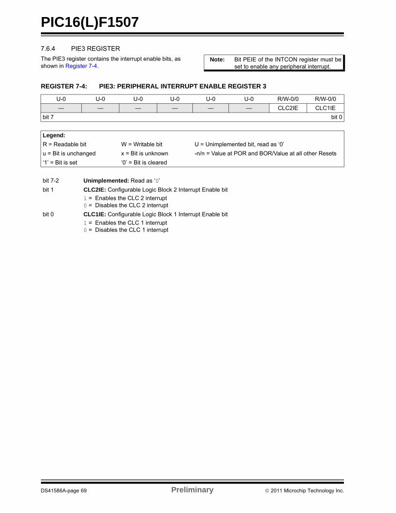
PIC16(L)F1507
7.6.4 PIE3 REGISTER
The PIE3 register contains the interrupt enable bits, asshown in Register 7-4.
Note: Bit PEIE of the INTCON register must beset to enable any peripheral interrupt.
REGISTER 7-4: PIE3: PERIPHERAL INTERRUPT ENABLE REGISTER 3
U-0 U-0 U-0 U-0 U-0 U-0 R/W-0/0 R/W-0/0
— — — — — — CLC2IE CLC1IE
bit 7 bit 0
Legend:
R = Readable bit W = Writable bit U = Unimplemented bit, read as ‘0’
u = Bit is unchanged x = Bit is unknown -n/n = Value at POR and BOR/Value at all other Resets
‘1’ = Bit is set ‘0’ = Bit is cleared
bit 7-2 Unimplemented: Read as ‘0’
bit 1 CLC2IE: Configurable Logic Block 2 Interrupt Enable bit
1 = Enables the CLC 2 interrupt0 = Disables the CLC 2 interrupt
bit 0 CLC1IE: Configurable Logic Block 1 Interrupt Enable bit
1 = Enables the CLC 1 interrupt0 = Disables the CLC 1 interrupt
DS41586A-page 69 Preliminary 2011 Microchip Technology Inc.
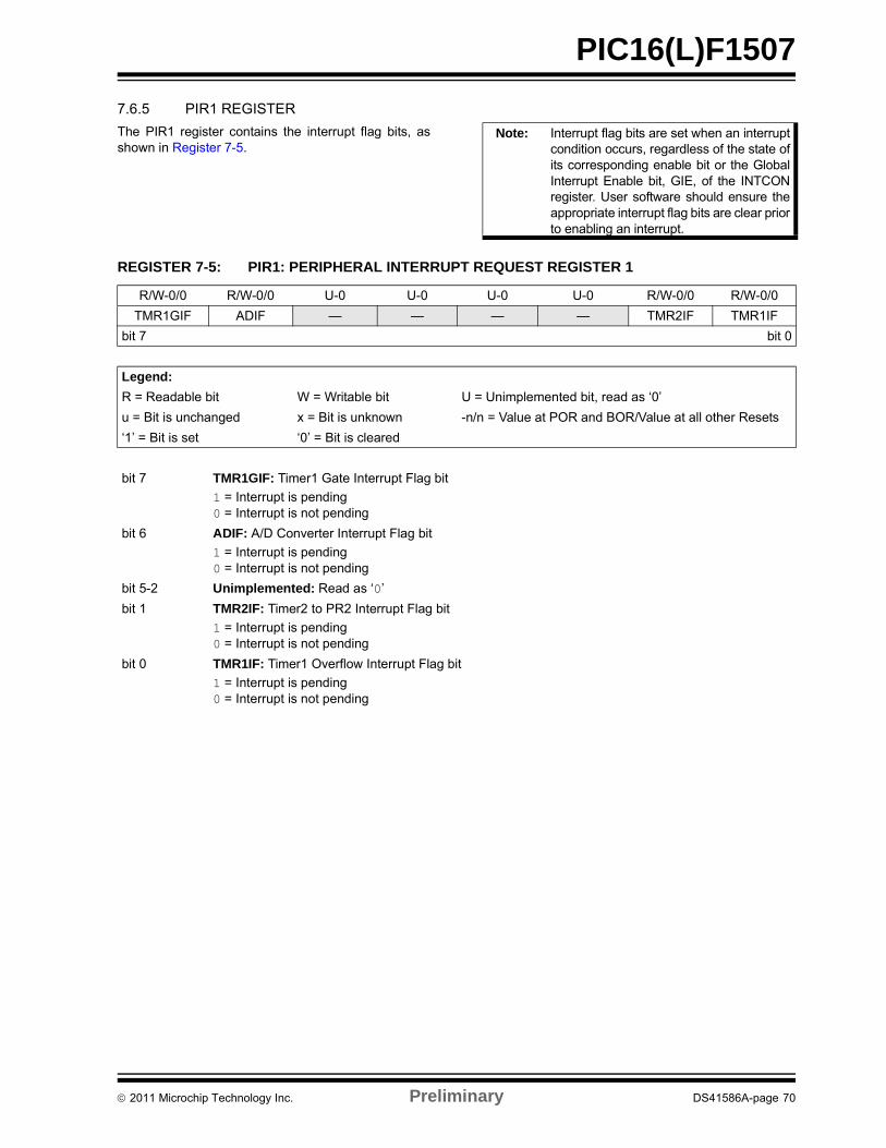
PIC16(L)F1507
7.6.5 PIR1 REGISTER
The PIR1 register contains the interrupt flag bits, asshown in Register 7-5.
Note: Interrupt flag bits are set when an interruptcondition occurs, regardless of the state ofits corresponding enable bit or the GlobalInterrupt Enable bit, GIE, of the INTCONregister. User software should ensure theappropriate interrupt flag bits are clear priorto enabling an interrupt.
REGISTER 7-5: PIR1: PERIPHERAL INTERRUPT REQUEST REGISTER 1
R/W-0/0 R/W-0/0 U-0 U-0 U-0 U-0 R/W-0/0 R/W-0/0
TMR1GIF ADIF — — — — TMR2IF TMR1IF
bit 7 bit 0
Legend:
R = Readable bit W = Writable bit U = Unimplemented bit, read as ‘0’
u = Bit is unchanged x = Bit is unknown -n/n = Value at POR and BOR/Value at all other Resets
‘1’ = Bit is set ‘0’ = Bit is cleared
bit 7 TMR1GIF: Timer1 Gate Interrupt Flag bit
1 = Interrupt is pending0 = Interrupt is not pending
bit 6 ADIF: A/D Converter Interrupt Flag bit
1 = Interrupt is pending0 = Interrupt is not pending
bit 5-2 Unimplemented: Read as ‘0’
bit 1 TMR2IF: Timer2 to PR2 Interrupt Flag bit
1 = Interrupt is pending0 = Interrupt is not pending
bit 0 TMR1IF: Timer1 Overflow Interrupt Flag bit
1 = Interrupt is pending0 = Interrupt is not pending
2011 Microchip Technology Inc. Preliminary DS41586A-page 70
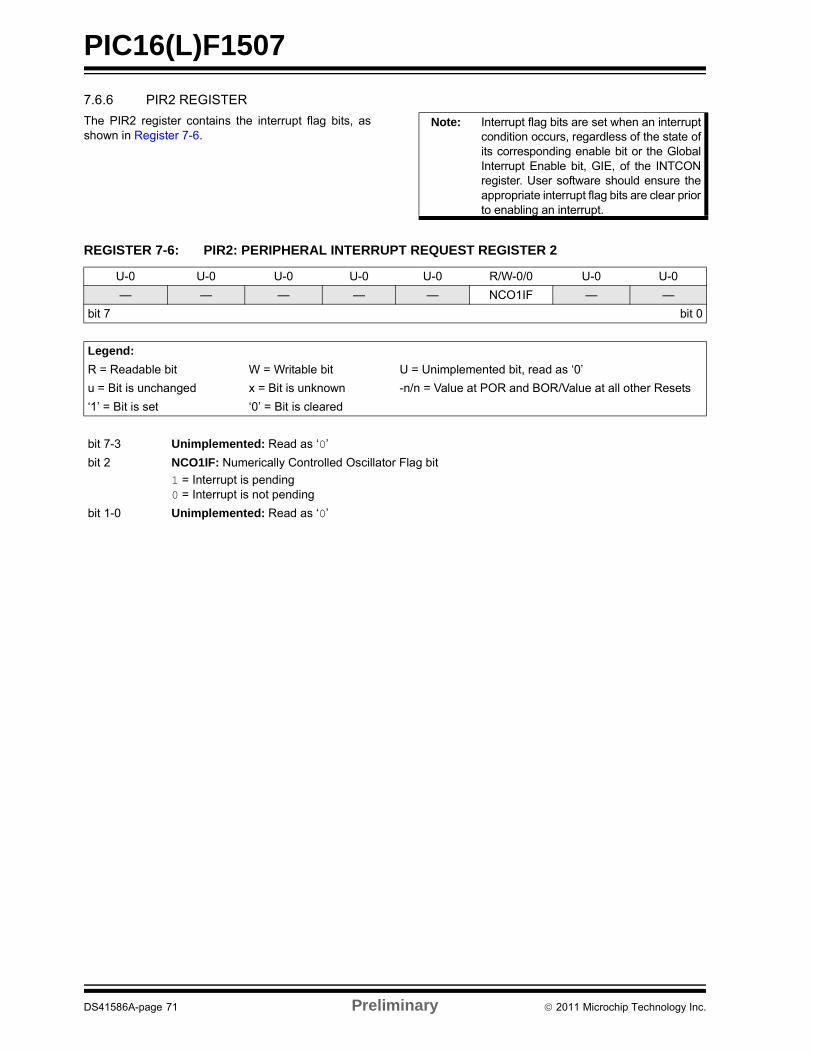
PIC16(L)F1507
7.6.6 PIR2 REGISTER
The PIR2 register contains the interrupt flag bits, asshown in Register 7-6.
Note: Interrupt flag bits are set when an interruptcondition occurs, regardless of the state ofits corresponding enable bit or the GlobalInterrupt Enable bit, GIE, of the INTCONregister. User software should ensure theappropriate interrupt flag bits are clear priorto enabling an interrupt.
REGISTER 7-6: PIR2: PERIPHERAL INTERRUPT REQUEST REGISTER 2
U-0 U-0 U-0 U-0 U-0 R/W-0/0 U-0 U-0
— — — — — NCO1IF — —
bit 7 bit 0
Legend:
R = Readable bit W = Writable bit U = Unimplemented bit, read as ‘0’
u = Bit is unchanged x = Bit is unknown -n/n = Value at POR and BOR/Value at all other Resets
‘1’ = Bit is set ‘0’ = Bit is cleared
bit 7-3 Unimplemented: Read as ‘0’
bit 2 NCO1IF: Numerically Controlled Oscillator Flag bit
1 = Interrupt is pending0 = Interrupt is not pending
bit 1-0 Unimplemented: Read as ‘0’
DS41586A-page 71 Preliminary 2011 Microchip Technology Inc.
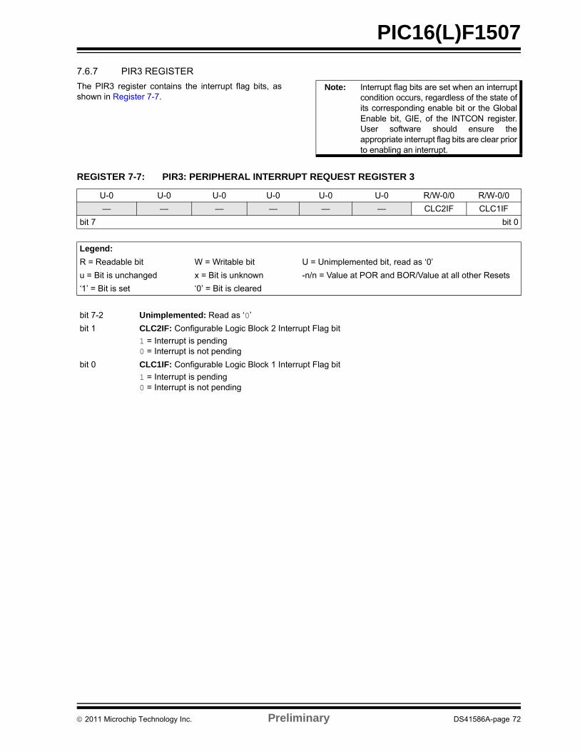
PIC16(L)F1507
7.6.7 PIR3 REGISTER
The PIR3 register contains the interrupt flag bits, asshown in Register 7-7.
Note: Interrupt flag bits are set when an interruptcondition occurs, regardless of the state ofits corresponding enable bit or the GlobalEnable bit, GIE, of the INTCON register.User software should ensure theappropriate interrupt flag bits are clear priorto enabling an interrupt.
REGISTER 7-7: PIR3: PERIPHERAL INTERRUPT REQUEST REGISTER 3
U-0 U-0 U-0 U-0 U-0 U-0 R/W-0/0 R/W-0/0
— — — — — — CLC2IF CLC1IF
bit 7 bit 0
Legend:
R = Readable bit W = Writable bit U = Unimplemented bit, read as ‘0’
u = Bit is unchanged x = Bit is unknown -n/n = Value at POR and BOR/Value at all other Resets
‘1’ = Bit is set ‘0’ = Bit is cleared
bit 7-2 Unimplemented: Read as ‘0’
bit 1 CLC2IF: Configurable Logic Block 2 Interrupt Flag bit
1 = Interrupt is pending0 = Interrupt is not pending
bit 0 CLC1IF: Configurable Logic Block 1 Interrupt Flag bit
1 = Interrupt is pending0 = Interrupt is not pending
2011 Microchip Technology Inc. Preliminary DS41586A-page 72
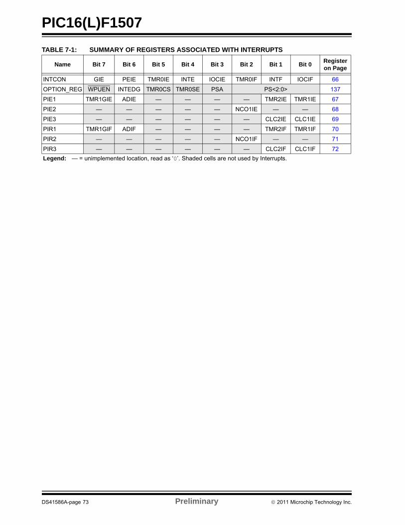
PIC16(L)F1507
TABLE 7-1: SUMMARY OF REGISTERS ASSOCIATED WITH INTERRUPTS
Name Bit 7 Bit 6 Bit 5 Bit 4 Bit 3 Bit 2 Bit 1 Bit 0Register on Page
INTCON GIE PEIE TMR0IE INTE IOCIE TMR0IF INTF IOCIF 66
OPTION_REG WPUEN INTEDG TMR0CS TMR0SE PSA PS<2:0> 137
PIE1 TMR1GIE ADIE — — — — TMR2IE TMR1IE 67
PIE2 — — — — — NCO1IE — — 68
PIE3 — — — — — — CLC2IE CLC1IE 69
PIR1 TMR1GIF ADIF — — — — TMR2IF TMR1IF 70
PIR2 — — — — — NCO1IF — — 71
PIR3 — — — — — — CLC2IF CLC1IF 72
Legend: — = unimplemented location, read as ‘0’. Shaded cells are not used by Interrupts.
DS41586A-page 73 Preliminary 2011 Microchip Technology Inc.

PIC16(L)F1507
NOTES:
2011 Microchip Technology Inc. Preliminary DS41586A-page 74
PIC16(L)F1507
8.0 POWER-DOWN MODE (SLEEP)
The Power-Down mode is entered by executing aSLEEP instruction.
Upon entering Sleep mode, the following conditions exist:
1. WDT will be cleared but keeps running, ifenabled for operation during Sleep.
2. PD bit of the STATUS register is cleared.
3. TO bit of the STATUS register is set.
4. CPU clock is disabled.
5. 31 kHz LFINTOSC is unaffected and peripheralsthat operate from it may continue operation inSleep.
6. ADC is unaffected, if the dedicated FRC clock isselected.
7. I/O ports maintain the status they had beforeSLEEP was executed (driving high, low or high-impedance).
8. Resets other than WDT are not affected bySleep mode.
Refer to individual chapters for more details onperipheral operation during Sleep.
To minimize current consumption, the followingconditions should be considered:
• I/O pins should not be floating
• External circuitry sinking current from I/O pins
• Internal circuitry sourcing current from I/O pins
• Current draw from pins with internal weak pull-ups
• Modules using 31 kHz LFINTOSC
• CWG, NCO and CLC modules using HFINTOSC
I/O pins that are high-impedance inputs should bepulled to VDD or VSS externally to avoid switchingcurrents caused by floating inputs.
Examples of internal circuitry that might be sourcingcurrent include the FVR module. See Section 13.0“Fixed Voltage Reference (FVR)” for moreinformation on this module.
8.1 Wake-up from Sleep
The device can wake-up from Sleep through one of thefollowing events:
1. External Reset input on MCLR pin, if enabled
2. BOR Reset, if enabled
3. POR Reset
4. Watchdog Timer, if enabled
5. Any external interrupt
6. Interrupts by peripherals capable of running dur-ing Sleep (see individual peripheral for moreinformation)
The first three events will cause a device Reset. Thelast three events are considered a continuation of pro-gram execution. To determine whether a device Resetor wake-up event occurred, refer to Section 6.11“Determining the Cause of a Reset”.
When the SLEEP instruction is being executed, the nextinstruction (PC + 1) is prefetched. For the device towake-up through an interrupt event, the correspondinginterrupt enable bit must be enabled. Wake-up willoccur regardless of the state of the GIE bit. If the GIEbit is disabled, the device continues execution at theinstruction after the SLEEP instruction. If the GIE bit isenabled, the device executes the instruction after theSLEEP instruction, the device will then call the InterruptService Routine. In cases where the execution of theinstruction following SLEEP is not desirable, the usershould have a NOP after the SLEEP instruction.
The WDT is cleared when the device wakes up fromSleep, regardless of the source of wake-up.
8.1.1 WAKE-UP USING INTERRUPTS
When global interrupts are disabled (GIE cleared) andany interrupt source has both its interrupt enable bitand interrupt flag bit set, one of the following will occur:
• If the interrupt occurs before the execution of a SLEEP instruction
- SLEEP instruction will execute as a NOP.
- WDT and WDT prescaler will not be cleared
- TO bit of the STATUS register will not be set
- PD bit of the STATUS register will not be cleared.
• If the interrupt occurs during or after the execu-tion of a SLEEP instruction
- SLEEP instruction will be completely exe-cuted
- Device will immediately wake-up from Sleep
- WDT and WDT prescaler will be cleared
- TO bit of the STATUS register will be set
- PD bit of the STATUS register will be cleared
DS41586A-page 75 Preliminary 2011 Microchip Technology Inc.
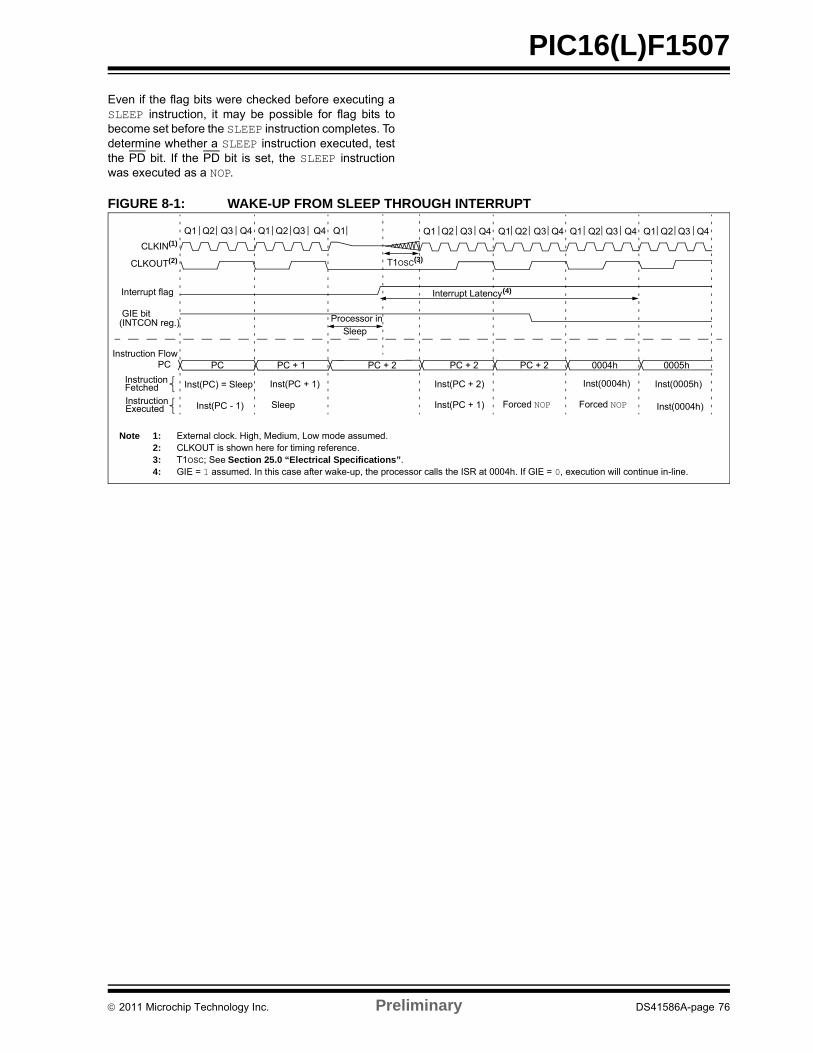
PIC16(L)F1507
Even if the flag bits were checked before executing aSLEEP instruction, it may be possible for flag bits tobecome set before the SLEEP instruction completes. Todetermine whether a SLEEP instruction executed, testthe PD bit. If the PD bit is set, the SLEEP instructionwas executed as a NOP.
FIGURE 8-1: WAKE-UP FROM SLEEP THROUGH INTERRUPT
Q1 Q2 Q3 Q4 Q1 Q2 Q3 Q4 Q1 Q1 Q2 Q3 Q4 Q1 Q2 Q3 Q4 Q1 Q2 Q3 Q4 Q1 Q2 Q3 Q4
CLKIN(1)
CLKOUT(2)
Interrupt flag
GIE bit(INTCON reg.)
Instruction FlowPC
InstructionFetched
InstructionExecuted
PC PC + 1 PC + 2
Inst(PC) = Sleep
Inst(PC - 1)
Inst(PC + 1)
Sleep
Processor inSleep
Interrupt Latency(4)
Inst(PC + 2)
Inst(PC + 1)
Inst(0004h) Inst(0005h)
Inst(0004h)Forced NOP
PC + 2 0004h 0005h
Forced NOP
T1OSC(3)
PC + 2
Note 1: External clock. High, Medium, Low mode assumed.2: CLKOUT is shown here for timing reference.3: T1OSC; See Section 25.0 “Electrical Specifications”.4: GIE = 1 assumed. In this case after wake-up, the processor calls the ISR at 0004h. If GIE = 0, execution will continue in-line.
2011 Microchip Technology Inc. Preliminary DS41586A-page 76
PIC16(L)F1507
8.2 Low-Power Sleep Mode
The PIC16(L)F1507 device contains an internal LowDropout (LDO) voltage regulator, which allows thedevice I/O pins to operate at voltages up to 5.5V whilethe internal device logic operates at a lower voltage.The LDO and its associated reference circuitry mustremain active when the device is in Sleep mode. ThePIC16(L)F1507 allows the user to optimize the operat-ing current in Sleep, depending on the applicationrequirements.
A Low-Power Sleep mode can be selected by settingthe VREGPM bit of the VREGCON register. With thisbit set, the LDO and reference circuitry are placed in alow-power state when the device is in Sleep.
8.2.1 SLEEP CURRENT VS. WAKE-UP TIME
In the default operating mode, the LDO and referencecircuitry remain in the normal configuration while inSleep. The device is able to exit Sleep mode quicklysince all circuits remain active. In Low-Power Sleepmode, when waking up from Sleep, an extra delay timeis required for these circuits to return to the normal con-figuration and stabilize.
The Low-Power Sleep mode is beneficial for applica-tions that stay in Sleep mode for long periods of time.The Normal mode is beneficial for applications thatneed to wake from Sleep quickly and frequently.
8.2.2 PERIPHERAL USAGE IN SLEEP
Some peripherals that can operate in Sleep mode willnot operate properly with the Low-Power Sleep modeselected. The LDO will remain in the Normal Powermode when those peripherals are enabled. The Low-Power Sleep mode is intended for use with theseperipherals:
• Brown-Out Reset (BOR)
• Watchdog Timer (WDT)
• External interrupt pin/Interrupt-on-change pins
• Timer1 (with external clock source)
The Complementary Waveform Generator (CWG), theNumerically Controlled Oscillator (NCO) and the Con-figurable Logic Cell (CLC) modules can utilize theHFINTOSC oscillator as either a clock source or as aninput source. Under certain conditions, when the HFIN-TOSC is selected for use with the CWG, NCO or CLCmodules, the HFINTOSC will remain active duringSleep. This will have a direct effect on the Sleep modecurrent.
Please refer to sections 20.5 “Operation DuringSleep”, 21.7 “Operation In Sleep” and 22.10 “Oper-ation During Sleep” for more information.
Note: The PIC16LF1507 does not have a con-figurable Low-Power Sleep mode.PIC16LF1507 is an unregulated deviceand is always in the lowest power statewhen in Sleep, with no wake-up time pen-alty. This device has a lower maximumVDD and I/O voltage than thePIC16(L)F1507. See Section 25.0 “Elec-trical Specifications” for more informa-tion.
DS41586A-page 77 Preliminary 2011 Microchip Technology Inc.
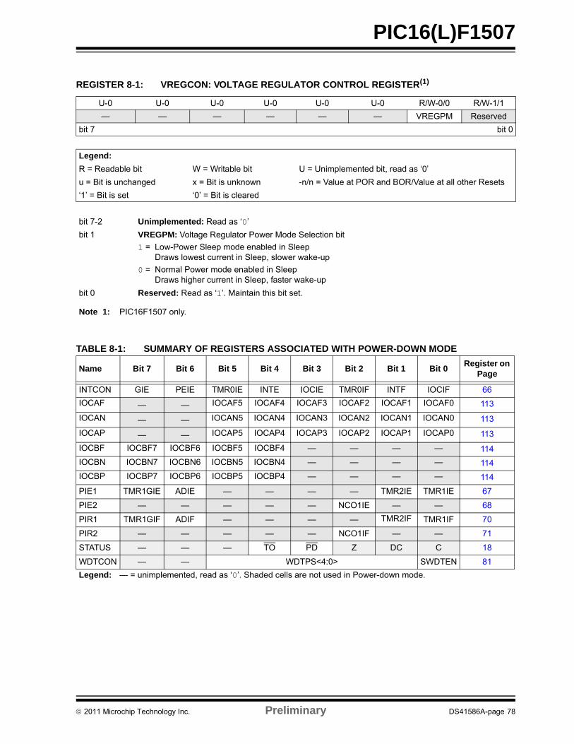
PIC16(L)F1507
TABLE 8-1: SUMMARY OF REGISTERS ASSOCIATED WITH POWER-DOWN MODE
REGISTER 8-1: VREGCON: VOLTAGE REGULATOR CONTROL REGISTER(1)
U-0 U-0 U-0 U-0 U-0 U-0 R/W-0/0 R/W-1/1
— — — — — — VREGPM Reserved
bit 7 bit 0
Legend:
R = Readable bit W = Writable bit U = Unimplemented bit, read as ‘0’
u = Bit is unchanged x = Bit is unknown -n/n = Value at POR and BOR/Value at all other Resets
‘1’ = Bit is set ‘0’ = Bit is cleared
bit 7-2 Unimplemented: Read as ‘0’
bit 1 VREGPM: Voltage Regulator Power Mode Selection bit
1 = Low-Power Sleep mode enabled in SleepDraws lowest current in Sleep, slower wake-up
0 = Normal Power mode enabled in SleepDraws higher current in Sleep, faster wake-up
bit 0 Reserved: Read as ‘1’. Maintain this bit set.
Note 1: PIC16F1507 only.
Name Bit 7 Bit 6 Bit 5 Bit 4 Bit 3 Bit 2 Bit 1 Bit 0Register on
Page
INTCON GIE PEIE TMR0IE INTE IOCIE TMR0IF INTF IOCIF 66
IOCAF — — IOCAF5 IOCAF4 IOCAF3 IOCAF2 IOCAF1 IOCAF0 113
IOCAN — — IOCAN5 IOCAN4 IOCAN3 IOCAN2 IOCAN1 IOCAN0 113
IOCAP — — IOCAP5 IOCAP4 IOCAP3 IOCAP2 IOCAP1 IOCAP0 113
IOCBF IOCBF7 IOCBF6 IOCBF5 IOCBF4 — — — — 114
IOCBN IOCBN7 IOCBN6 IOCBN5 IOCBN4 — — — — 114
IOCBP IOCBP7 IOCBP6 IOCBP5 IOCBP4 — — — — 114
PIE1 TMR1GIE ADIE — — — — TMR2IE TMR1IE 67
PIE2 — — — — — NCO1IE — — 68
PIR1 TMR1GIF ADIF — — — — TMR2IF TMR1IF 70
PIR2 — — — — — NCO1IF — — 71
STATUS — — — TO PD Z DC C 18
WDTCON — — WDTPS<4:0> SWDTEN 81
Legend: — = unimplemented, read as ‘0’. Shaded cells are not used in Power-down mode.
2011 Microchip Technology Inc. Preliminary DS41586A-page 78
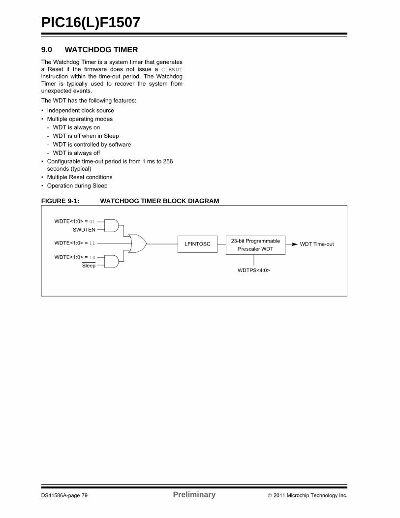
PIC16(L)F1507
9.0 WATCHDOG TIMER
The Watchdog Timer is a system timer that generatesa Reset if the firmware does not issue a CLRWDTinstruction within the time-out period. The WatchdogTimer is typically used to recover the system fromunexpected events.
The WDT has the following features:
• Independent clock source
• Multiple operating modes
- WDT is always on
- WDT is off when in Sleep
- WDT is controlled by software
- WDT is always off
• Configurable time-out period is from 1 ms to 256 seconds (typical)
• Multiple Reset conditions
• Operation during Sleep
FIGURE 9-1: WATCHDOG TIMER BLOCK DIAGRAM
LFINTOSC23-bit Programmable
Prescaler WDTWDT Time-out
WDTPS<4:0>
SWDTEN
Sleep
WDTE<1:0> = 11
WDTE<1:0> = 01
WDTE<1:0> = 10
DS41586A-page 79 Preliminary 2011 Microchip Technology Inc.
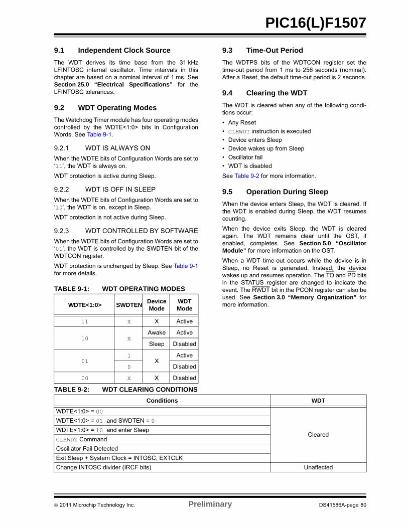
PIC16(L)F1507
9.1 Independent Clock Source
The WDT derives its time base from the 31 kHzLFINTOSC internal oscillator. Time intervals in thischapter are based on a nominal interval of 1 ms. SeeSection 25.0 “Electrical Specifications” for theLFINTOSC tolerances.
9.2 WDT Operating Modes
The Watchdog Timer module has four operating modescontrolled by the WDTE<1:0> bits in ConfigurationWords. See Table 9-1.
9.2.1 WDT IS ALWAYS ON
When the WDTE bits of Configuration Words are set to‘11’, the WDT is always on.
WDT protection is active during Sleep.
9.2.2 WDT IS OFF IN SLEEP
When the WDTE bits of Configuration Words are set to‘10’, the WDT is on, except in Sleep.
WDT protection is not active during Sleep.
9.2.3 WDT CONTROLLED BY SOFTWARE
When the WDTE bits of Configuration Words are set to‘01’, the WDT is controlled by the SWDTEN bit of theWDTCON register.
WDT protection is unchanged by Sleep. See Table 9-1for more details.
TABLE 9-1: WDT OPERATING MODES
9.3 Time-Out Period
The WDTPS bits of the WDTCON register set thetime-out period from 1 ms to 256 seconds (nominal).After a Reset, the default time-out period is 2 seconds.
9.4 Clearing the WDT
The WDT is cleared when any of the following condi-tions occur:
• Any Reset
• CLRWDT instruction is executed
• Device enters Sleep
• Device wakes up from Sleep
• Oscillator fail
• WDT is disabled
See Table 9-2 for more information.
9.5 Operation During Sleep
When the device enters Sleep, the WDT is cleared. Ifthe WDT is enabled during Sleep, the WDT resumescounting.
When the device exits Sleep, the WDT is clearedagain. The WDT remains clear until the OST, ifenabled, completes. See Section 5.0 “OscillatorModule” for more information on the OST.
When a WDT time-out occurs while the device is inSleep, no Reset is generated. Instead, the devicewakes up and resumes operation. The TO and PD bitsin the STATUS register are changed to indicate theevent. The RWDT bit in the PCON register can also beused. See Section 3.0 “Memory Organization” formore information.WDTE<1:0> SWDTEN
Device Mode
WDT Mode
11 X X Active
10 XAwake Active
Sleep Disabled
011
XActive
0 Disabled
00 X X Disabled
TABLE 9-2: WDT CLEARING CONDITIONS
Conditions WDT
WDTE<1:0> = 00
Cleared
WDTE<1:0> = 01 and SWDTEN = 0
WDTE<1:0> = 10 and enter Sleep
CLRWDT Command
Oscillator Fail Detected
Exit Sleep + System Clock = INTOSC, EXTCLK
Change INTOSC divider (IRCF bits) Unaffected
2011 Microchip Technology Inc. Preliminary DS41586A-page 80
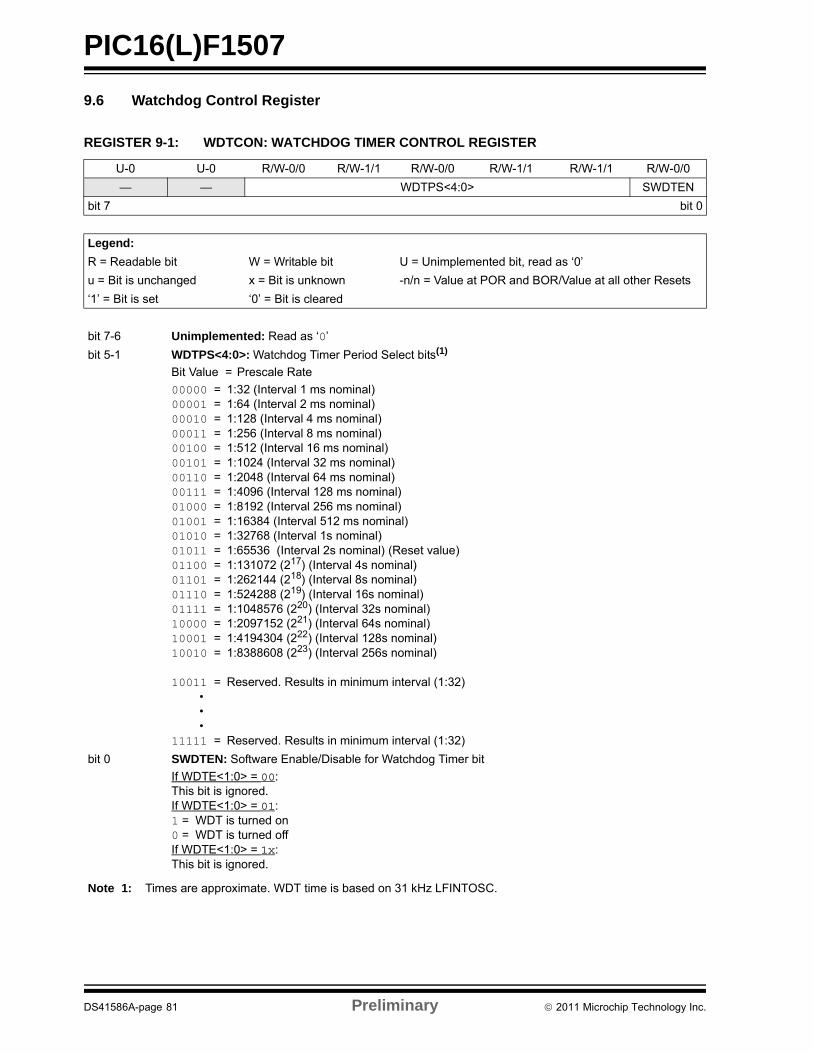
PIC16(L)F1507
9.6 Watchdog Control Register
REGISTER 9-1: WDTCON: WATCHDOG TIMER CONTROL REGISTER
U-0 U-0 R/W-0/0 R/W-1/1 R/W-0/0 R/W-1/1 R/W-1/1 R/W-0/0
— — WDTPS<4:0> SWDTEN
bit 7 bit 0
Legend:
R = Readable bit W = Writable bit U = Unimplemented bit, read as ‘0’
u = Bit is unchanged x = Bit is unknown -n/n = Value at POR and BOR/Value at all other Resets
‘1’ = Bit is set ‘0’ = Bit is cleared
bit 7-6 Unimplemented: Read as ‘0’
bit 5-1 WDTPS<4:0>: Watchdog Timer Period Select bits(1)
Bit Value = Prescale Rate
00000 = 1:32 (Interval 1 ms nominal)00001 = 1:64 (Interval 2 ms nominal)00010 = 1:128 (Interval 4 ms nominal)00011 = 1:256 (Interval 8 ms nominal)00100 = 1:512 (Interval 16 ms nominal)00101 = 1:1024 (Interval 32 ms nominal)00110 = 1:2048 (Interval 64 ms nominal)00111 = 1:4096 (Interval 128 ms nominal)01000 = 1:8192 (Interval 256 ms nominal)01001 = 1:16384 (Interval 512 ms nominal)01010 = 1:32768 (Interval 1s nominal)01011 = 1:65536 (Interval 2s nominal) (Reset value)01100 = 1:131072 (217) (Interval 4s nominal)01101 = 1:262144 (218) (Interval 8s nominal)01110 = 1:524288 (219) (Interval 16s nominal)01111 = 1:1048576 (220) (Interval 32s nominal)10000 = 1:2097152 (221) (Interval 64s nominal)10001 = 1:4194304 (222) (Interval 128s nominal)10010 = 1:8388608 (223) (Interval 256s nominal)
10011 = Reserved. Results in minimum interval (1:32) • • •
11111 = Reserved. Results in minimum interval (1:32)
bit 0 SWDTEN: Software Enable/Disable for Watchdog Timer bit
If WDTE<1:0> = 00:This bit is ignored.If WDTE<1:0> = 01:1 = WDT is turned on0 = WDT is turned offIf WDTE<1:0> = 1x:This bit is ignored.
Note 1: Times are approximate. WDT time is based on 31 kHz LFINTOSC.
DS41586A-page 81 Preliminary 2011 Microchip Technology Inc.
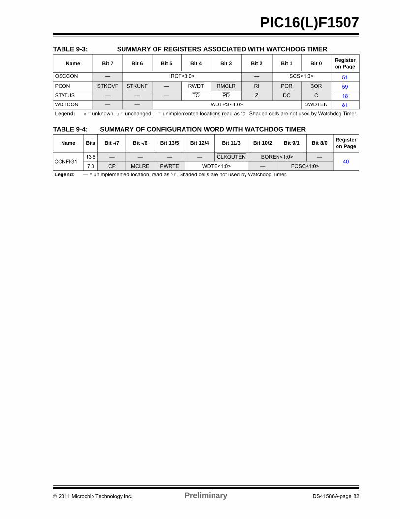
PIC16(L)F1507
TABLE 9-3: SUMMARY OF REGISTERS ASSOCIATED WITH WATCHDOG TIMER
TABLE 9-4: SUMMARY OF CONFIGURATION WORD WITH WATCHDOG TIMER
Name Bit 7 Bit 6 Bit 5 Bit 4 Bit 3 Bit 2 Bit 1 Bit 0Register on Page
OSCCON — IRCF<3:0> — SCS<1:0> 51
PCON STKOVF STKUNF — RWDT RMCLR RI POR BOR 59
STATUS — — — TO PD Z DC C 18
WDTCON — — WDTPS<4:0> SWDTEN 81
Legend: x = unknown, u = unchanged, – = unimplemented locations read as ‘0’. Shaded cells are not used by Watchdog Timer.
Name Bits Bit -/7 Bit -/6 Bit 13/5 Bit 12/4 Bit 11/3 Bit 10/2 Bit 9/1 Bit 8/0Register on Page
CONFIG113:8 — — — — CLKOUTEN BOREN<1:0> —
407:0 CP MCLRE PWRTE WDTE<1:0> — FOSC<1:0>
Legend: — = unimplemented location, read as ‘0’. Shaded cells are not used by Watchdog Timer.
2011 Microchip Technology Inc. Preliminary DS41586A-page 82
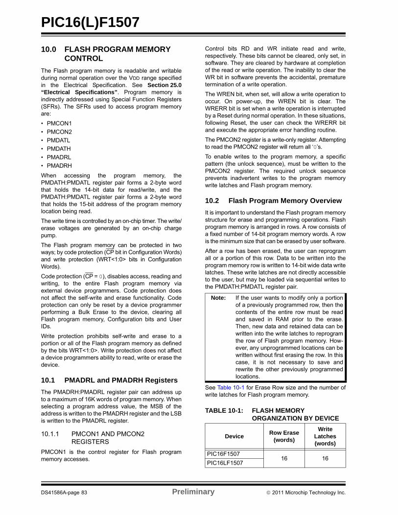
PIC16(L)F1507
10.0 FLASH PROGRAM MEMORY CONTROL
The Flash program memory is readable and writableduring normal operation over the VDD range specifiedin the Electrical Specification. See Section 25.0“Electrical Specifications”. Program memory isindirectly addressed using Special Function Registers(SFRs). The SFRs used to access program memoryare:
• PMCON1
• PMCON2
• PMDATL
• PMDATH
• PMADRL
• PMADRH
When accessing the program memory, thePMDATH:PMDATL register pair forms a 2-byte wordthat holds the 14-bit data for read/write, and thePMDATH:PMDATL register pair forms a 2-byte wordthat holds the 15-bit address of the program memorylocation being read.
The write time is controlled by an on-chip timer. The write/erase voltages are generated by an on-chip chargepump.
The Flash program memory can be protected in twoways; by code protection (CP bit in Configuration Words)and write protection (WRT<1:0> bits in ConfigurationWords).
Code protection (CP = 0), disables access, reading andwriting, to the entire Flash program memory viaexternal device programmers. Code protection doesnot affect the self-write and erase functionality. Codeprotection can only be reset by a device programmerperforming a Bulk Erase to the device, clearing allFlash program memory, Configuration bits and UserIDs.
Write protection prohibits self-write and erase to aportion or all of the Flash program memory as definedby the bits WRT<1:0>. Write protection does not affecta device programmers ability to read, write or erase thedevice.
10.1 PMADRL and PMADRH Registers
The PMADRH:PMADRL register pair can address upto a maximum of 16K words of program memory. Whenselecting a program address value, the MSB of theaddress is written to the PMADRH register and the LSBis written to the PMADRL register.
10.1.1 PMCON1 AND PMCON2 REGISTERS
PMCON1 is the control register for Flash programmemory accesses.
Control bits RD and WR initiate read and write,respectively. These bits cannot be cleared, only set, insoftware. They are cleared by hardware at completionof the read or write operation. The inability to clear theWR bit in software prevents the accidental, prematuretermination of a write operation.
The WREN bit, when set, will allow a write operation tooccur. On power-up, the WREN bit is clear. TheWRERR bit is set when a write operation is interruptedby a Reset during normal operation. In these situations,following Reset, the user can check the WRERR bitand execute the appropriate error handling routine.
The PMCON2 register is a write-only register. Attemptingto read the PMCON2 register will return all ‘0’s.
To enable writes to the program memory, a specificpattern (the unlock sequence), must be written to thePMCON2 register. The required unlock sequenceprevents inadvertent writes to the program memorywrite latches and Flash program memory.
10.2 Flash Program Memory Overview
It is important to understand the Flash program memorystructure for erase and programming operations. Flashprogram memory is arranged in rows. A row consists ofa fixed number of 14-bit program memory words. A rowis the minimum size that can be erased by user software.
After a row has been erased, the user can reprogramall or a portion of this row. Data to be written into theprogram memory row is written to 14-bit wide data writelatches. These write latches are not directly accessibleto the user, but may be loaded via sequential writes tothe PMDATH:PMDATL register pair.
See Table 10-1 for Erase Row size and the number ofwrite latches for Flash program memory.
Note: If the user wants to modify only a portionof a previously programmed row, then thecontents of the entire row must be readand saved in RAM prior to the erase.Then, new data and retained data can bewritten into the write latches to reprogramthe row of Flash program memory. How-ever, any unprogrammed locations can bewritten without first erasing the row. In thiscase, it is not necessary to save andrewrite the other previously programmedlocations.
TABLE 10-1: FLASH MEMORY ORGANIZATION BY DEVICE
DeviceRow Erase
(words)
Write Latches (words)
PIC16F150716 16
PIC16LF1507
DS41586A-page 83 Preliminary 2011 Microchip Technology Inc.
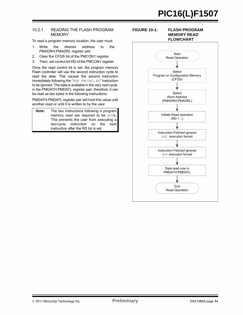
PIC16(L)F1507
10.2.1 READING THE FLASH PROGRAM MEMORY
To read a program memory location, the user must:
1. Write the desired address to thePMADRH:PMADRL register pair.
2. Clear the CFGS bit of the PMCON1 register.
3. Then, set control bit RD of the PMCON1 register.
Once the read control bit is set, the program memoryFlash controller will use the second instruction cycle toread the data. This causes the second instructionimmediately following the “BSF PMCON1,RD” instructionto be ignored. The data is available in the very next cycle,in the PMDATH:PMDATL register pair; therefore, it canbe read as two bytes in the following instructions.
PMDATH:PMDATL register pair will hold this value untilanother read or until it is written to by the user.
FIGURE 10-1: FLASH PROGRAM MEMORY READ FLOWCHART
Note: The two instructions following a programmemory read are required to be NOPs.This prevents the user from executing atwo-cycle instruction on the nextinstruction after the RD bit is set.
Start Read Operation
Select Program or Configuration Memory
(CFGS)
Select Word Address
(PMADRH:PMADRL)
End Read Operation
Instruction Fetched ignoredNOP execution forced
Instruction Fetched ignoredNOP execution forced
Initiate Read operation(RD = 1)
Data read now in PMDATH:PMDATL
2011 Microchip Technology Inc. Preliminary DS41586A-page 84
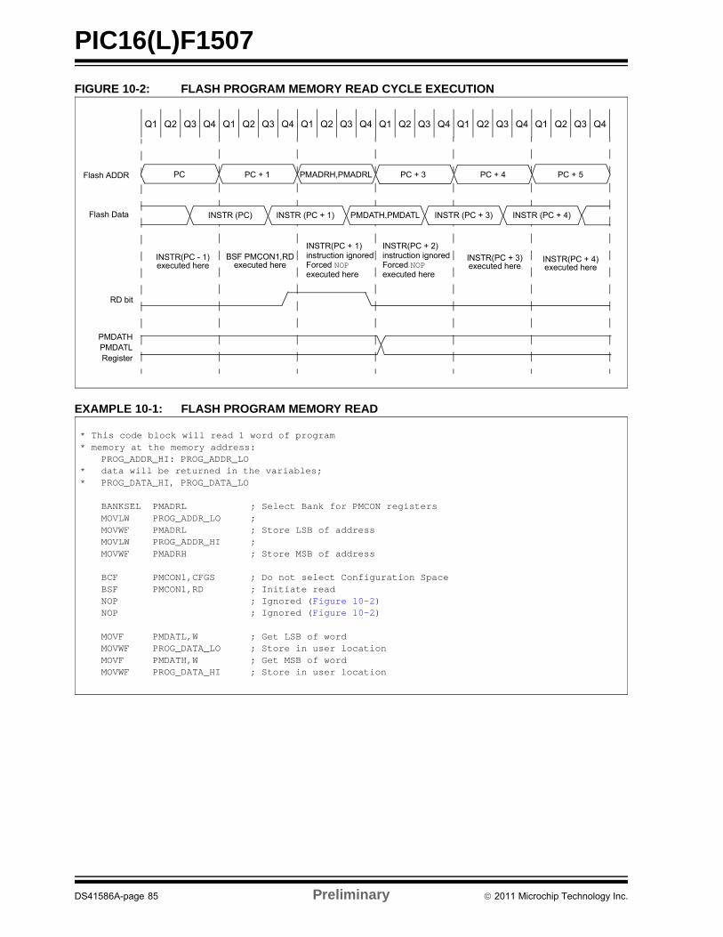
PIC16(L)F1507
FIGURE 10-2: FLASH PROGRAM MEMORY READ CYCLE EXECUTION
EXAMPLE 10-1: FLASH PROGRAM MEMORY READ
Q1 Q2 Q3 Q4 Q1 Q2 Q3 Q4 Q1 Q2 Q3 Q4 Q1 Q2 Q3 Q4 Q1 Q2 Q3 Q4 Q1 Q2 Q3 Q4
BSF PMCON1,RDexecuted here
INSTR(PC + 1)
executed here
PC PC + 1 PMADRH,PMADRL PC+3 PC + 5Flash ADDR
RD bit
PMDATH,PMDATL
PC + 3 PC + 4
INSTR (PC + 1)
INSTR(PC - 1)executed here
INSTR(PC + 3)executed here
INSTR(PC + 4)executed here
Flash Data
PMDATHPMDATLRegister
INSTR (PC) INSTR (PC + 3) INSTR (PC + 4)
instruction ignoredForced NOP
INSTR(PC + 2)
executed here
instruction ignoredForced NOP
* This code block will read 1 word of program* memory at the memory address:
PROG_ADDR_HI: PROG_ADDR_LO* data will be returned in the variables;* PROG_DATA_HI, PROG_DATA_LO
BANKSEL PMADRL ; Select Bank for PMCON registersMOVLW PROG_ADDR_LO ; MOVWF PMADRL ; Store LSB of addressMOVLW PROG_ADDR_HI ; MOVWF PMADRH ; Store MSB of address
BCF PMCON1,CFGS ; Do not select Configuration SpaceBSF PMCON1,RD ; Initiate readNOP ; Ignored (Figure 10-2)NOP ; Ignored (Figure 10-2)
MOVF PMDATL,W ; Get LSB of wordMOVWF PROG_DATA_LO ; Store in user locationMOVF PMDATH,W ; Get MSB of wordMOVWF PROG_DATA_HI ; Store in user location
DS41586A-page 85 Preliminary 2011 Microchip Technology Inc.
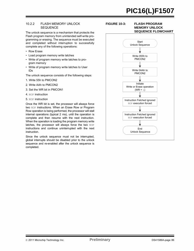
PIC16(L)F1507
10.2.2 FLASH MEMORY UNLOCK SEQUENCE
The unlock sequence is a mechanism that protects theFlash program memory from unintended self-write pro-gramming or erasing. The sequence must be executedand completed without interruption to successfullycomplete any of the following operations:
• Row Erase
• Load program memory write latches
• Write of program memory write latches to pro-gram memory
• Write of program memory write latches to User IDs
The unlock sequence consists of the following steps:
1. Write 55h to PMCON2
2. Write AAh to PMCON2
3. Set the WR bit in PMCON1
4. NOP instruction
5. NOP instruction
Once the WR bit is set, the processor will always forcetwo NOP instructions. When an Erase Row or ProgramRow operation is being performed, the processor will stallinternal operations (typical 2 ms), until the operation iscomplete and then resume with the next instruction.When the operation is loading the program memory writelatches, the processor will always force the two NOPinstructions and continue uninterrupted with the nextinstruction.
Since the unlock sequence must not be interrupted,global interrupts should be disabled prior to the unlocksequence and re-enabled after the unlock sequence iscompleted.
FIGURE 10-3: FLASH PROGRAM MEMORY UNLOCK SEQUENCE FLOWCHART
Write 055h to PMCON2
Start Unlock Sequence
Write 0AAh toPMCON2
InitiateWrite or Erase operation
(WR = 1)
Instruction Fetched ignoredNOP execution forced
End Unlock Sequence
Instruction Fetched ignoredNOP execution forced
2011 Microchip Technology Inc. Preliminary DS41586A-page 86
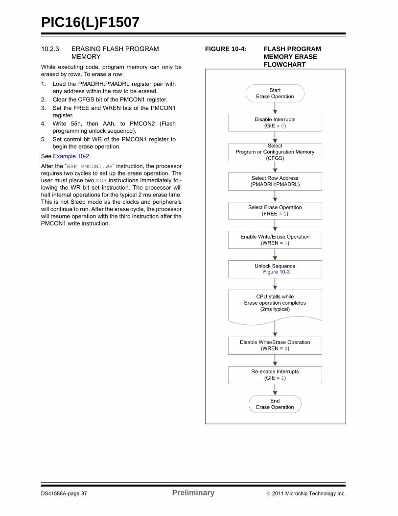
PIC16(L)F1507
10.2.3 ERASING FLASH PROGRAM MEMORY
While executing code, program memory can only beerased by rows. To erase a row:
1. Load the PMADRH:PMADRL register pair withany address within the row to be erased.
2. Clear the CFGS bit of the PMCON1 register.
3. Set the FREE and WREN bits of the PMCON1register.
4. Write 55h, then AAh, to PMCON2 (Flashprogramming unlock sequence).
5. Set control bit WR of the PMCON1 register tobegin the erase operation.
See Example 10-2.
After the “BSF PMCON1,WR” instruction, the processorrequires two cycles to set up the erase operation. Theuser must place two NOP instructions immediately fol-lowing the WR bit set instruction. The processor willhalt internal operations for the typical 2 ms erase time.This is not Sleep mode as the clocks and peripheralswill continue to run. After the erase cycle, the processorwill resume operation with the third instruction after thePMCON1 write instruction.
FIGURE 10-4: FLASH PROGRAM MEMORY ERASE FLOWCHART
Disable Interrupts(GIE = 0)
Start Erase Operation
Select Program or Configuration Memory
(CFGS)
Select Row Address(PMADRH:PMADRL)
Select Erase Operation(FREE = 1)
Enable Write/Erase Operation (WREN = 1)
Unlock Sequence(FIGURE x-x)
Disable Write/Erase Operation (WREN = 0)
Re-enable Interrupts(GIE = 1)
End Erase Operation
CPU stalls while Erase operation completes
(2ms typical)
Figure 10-3
DS41586A-page 87 Preliminary 2011 Microchip Technology Inc.
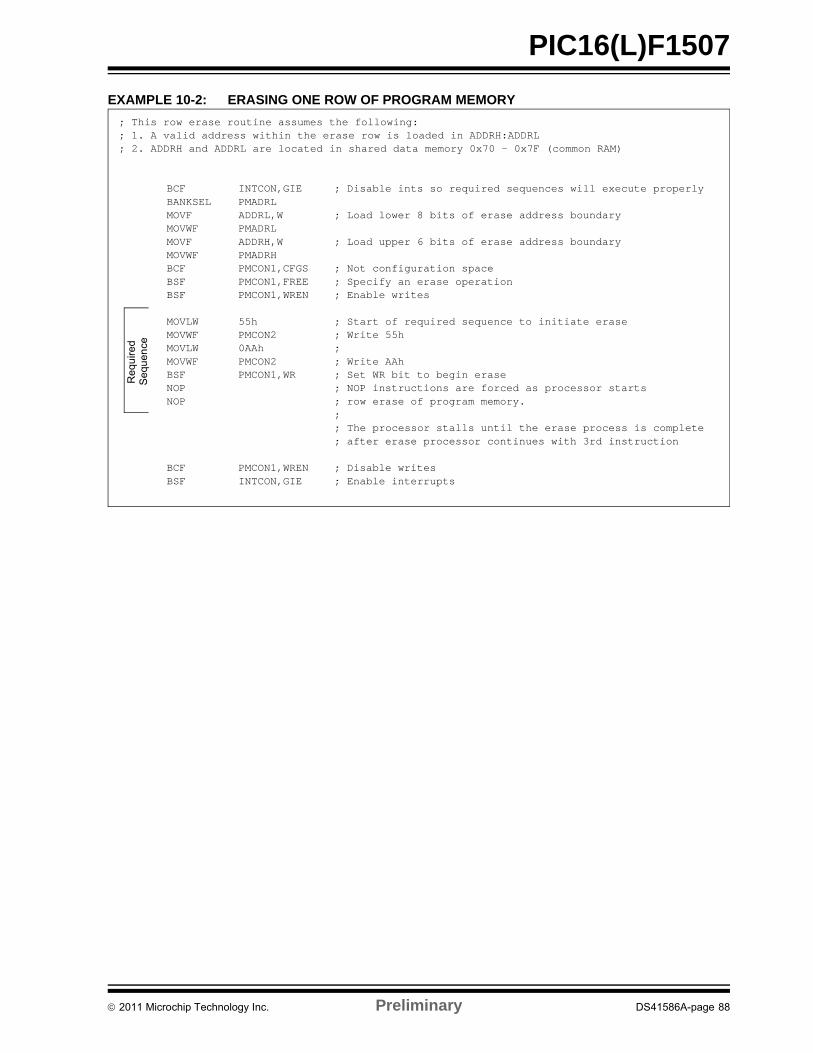
PIC16(L)F1507
EXAMPLE 10-2: ERASING ONE ROW OF PROGRAM MEMORY
; This row erase routine assumes the following:; 1. A valid address within the erase row is loaded in ADDRH:ADDRL; 2. ADDRH and ADDRL are located in shared data memory 0x70 - 0x7F (common RAM)
BCF INTCON,GIE ; Disable ints so required sequences will execute properlyBANKSEL PMADRLMOVF ADDRL,W ; Load lower 8 bits of erase address boundaryMOVWF PMADRLMOVF ADDRH,W ; Load upper 6 bits of erase address boundaryMOVWF PMADRHBCF PMCON1,CFGS ; Not configuration spaceBSF PMCON1,FREE ; Specify an erase operationBSF PMCON1,WREN ; Enable writes
MOVLW 55h ; Start of required sequence to initiate eraseMOVWF PMCON2 ; Write 55hMOVLW 0AAh ;MOVWF PMCON2 ; Write AAhBSF PMCON1,WR ; Set WR bit to begin eraseNOP ; NOP instructions are forced as processor startsNOP ; row erase of program memory.
;; The processor stalls until the erase process is complete; after erase processor continues with 3rd instruction
BCF PMCON1,WREN ; Disable writesBSF INTCON,GIE ; Enable interrupts
Re
qu
ire
dS
eq
ue
nce
2011 Microchip Technology Inc. Preliminary DS41586A-page 88
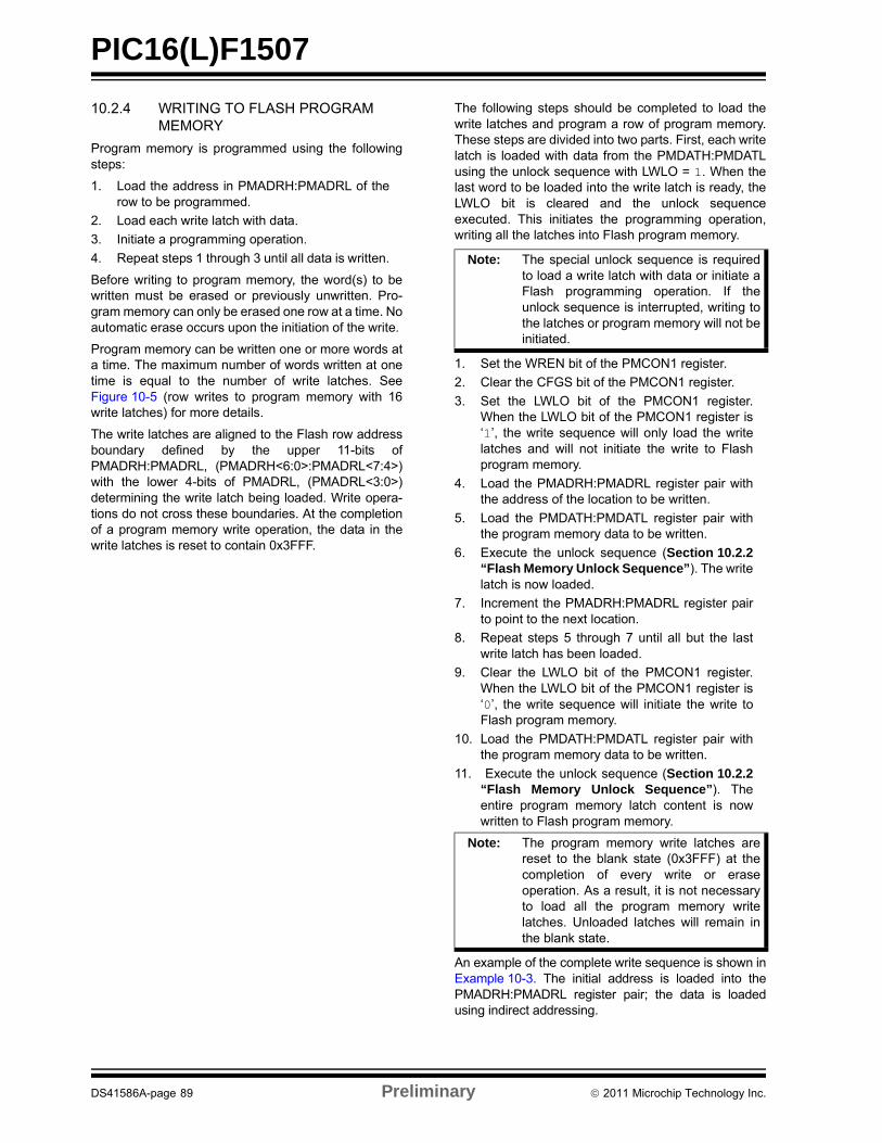
PIC16(L)F1507
10.2.4 WRITING TO FLASH PROGRAM MEMORY
Program memory is programmed using the followingsteps:
1. Load the address in PMADRH:PMADRL of therow to be programmed.
2. Load each write latch with data.
3. Initiate a programming operation.
4. Repeat steps 1 through 3 until all data is written.
Before writing to program memory, the word(s) to bewritten must be erased or previously unwritten. Pro-gram memory can only be erased one row at a time. Noautomatic erase occurs upon the initiation of the write.
Program memory can be written one or more words ata time. The maximum number of words written at onetime is equal to the number of write latches. SeeFigure 10-5 (row writes to program memory with 16write latches) for more details.
The write latches are aligned to the Flash row addressboundary defined by the upper 11-bits ofPMADRH:PMADRL, (PMADRH<6:0>:PMADRL<7:4>)with the lower 4-bits of PMADRL, (PMADRL<3:0>)determining the write latch being loaded. Write opera-tions do not cross these boundaries. At the completionof a program memory write operation, the data in thewrite latches is reset to contain 0x3FFF.
The following steps should be completed to load thewrite latches and program a row of program memory.These steps are divided into two parts. First, each writelatch is loaded with data from the PMDATH:PMDATLusing the unlock sequence with LWLO = 1. When thelast word to be loaded into the write latch is ready, theLWLO bit is cleared and the unlock sequenceexecuted. This initiates the programming operation,writing all the latches into Flash program memory.
1. Set the WREN bit of the PMCON1 register.
2. Clear the CFGS bit of the PMCON1 register.
3. Set the LWLO bit of the PMCON1 register.When the LWLO bit of the PMCON1 register is‘1’, the write sequence will only load the writelatches and will not initiate the write to Flashprogram memory.
4. Load the PMADRH:PMADRL register pair withthe address of the location to be written.
5. Load the PMDATH:PMDATL register pair withthe program memory data to be written.
6. Execute the unlock sequence (Section 10.2.2“Flash Memory Unlock Sequence”). The writelatch is now loaded.
7. Increment the PMADRH:PMADRL register pairto point to the next location.
8. Repeat steps 5 through 7 until all but the lastwrite latch has been loaded.
9. Clear the LWLO bit of the PMCON1 register.When the LWLO bit of the PMCON1 register is‘0’, the write sequence will initiate the write toFlash program memory.
10. Load the PMDATH:PMDATL register pair withthe program memory data to be written.
11. Execute the unlock sequence (Section 10.2.2“Flash Memory Unlock Sequence”). Theentire program memory latch content is nowwritten to Flash program memory.
An example of the complete write sequence is shown inExample 10-3. The initial address is loaded into thePMADRH:PMADRL register pair; the data is loadedusing indirect addressing.
Note: The special unlock sequence is requiredto load a write latch with data or initiate aFlash programming operation. If theunlock sequence is interrupted, writing tothe latches or program memory will not beinitiated.
Note: The program memory write latches arereset to the blank state (0x3FFF) at thecompletion of every write or eraseoperation. As a result, it is not necessaryto load all the program memory writelatches. Unloaded latches will remain inthe blank state.
DS41586A-page 89 Preliminary 2011 Microchip Technology Inc.
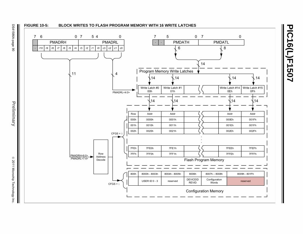
PIC
16(L)F
1507
DS
41
58
6A
-pa
ge
90
Prelim
inary
2
01
1 M
icroch
ip T
ech
no
log
y Inc.
PMDATL
0
8
Write Latch #150Fh
1414
14
Memory
Write Latch #140Eh
AddrAddr
001Fh000Eh
001Fh001Eh
002Fh002Eh
7FEFh7FEEh
7FFFh7FFEh
14
8009h - 801Fh
onfigurationWords
007h – 8008h
reserved
Memory
FIGURE 10-5: BLOCK WRITES TO FLASH PROGRAM MEMORY WITH 16 WRITE LATCHES
PMDATH
7 5 0 7
6
14
1414
PMADRH PMADRL
7 6 0 7 5 4 0
Program Memory Write Latches
14 14
411
PMADRH<6:0>:PMADRL<7:4> Flash Program
Row
Row Address Decode
Addr
Write Latch #101h
Write Latch #000h
Addr
000h 0000h 0001h
001h 0010h 0011h
002h 0020h 0021h
7FEh 7FE0h 7FE1h
7FFh 7FF0h 7FF1h
r9 r8 r7 r6 r5 r4 r3- r1 r0 c3 c2 c1 c0r2
PMADRL<4:0>
800h 8000h - 8003h
CUSER ID 0 - 3
88006h
DEVICEIDREVID
reserved
8004h - 8005h
Configuration
CFGS = 0
CFGS = 1
--
r10
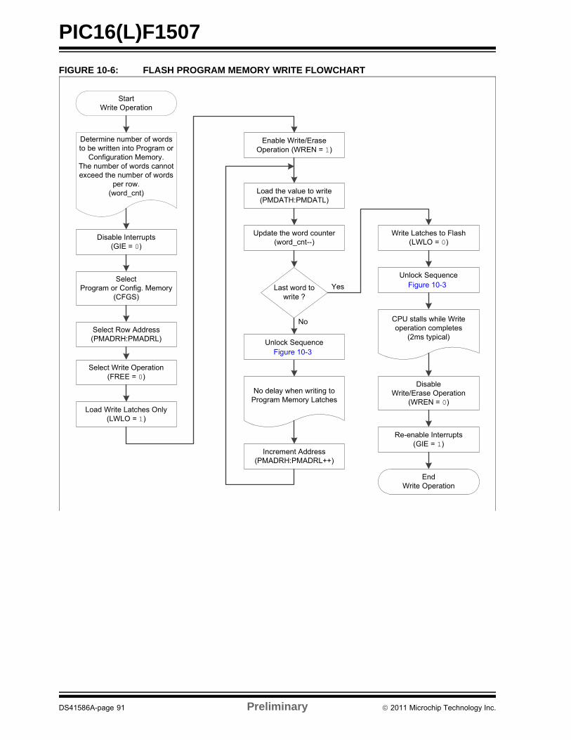
PIC16(L)F1507
FIGURE 10-6: FLASH PROGRAM MEMORY WRITE FLOWCHART
Disable Interrupts(GIE = 0)
Start Write Operation
Select Program or Config. Memory
(CFGS)
Select Row Address(PMADRH:PMADRL)
Select Write Operation(FREE = 0)
Enable Write/Erase Operation (WREN = 1)
Unlock Sequence(Figure x-x)
Disable Write/Erase Operation
(WREN = 0)
Re-enable Interrupts(GIE = 1)
End Write Operation
No delay when writing to Program Memory Latches
Determine number of words to be written into Program or
Configuration Memory. The number of words cannot exceed the number of words
per row.(word_cnt) Load the value to write
(PMDATH:PMDATL)
Update the word counter (word_cnt--)
Last word to write ?
Increment Address(PMADRH:PMADRL++)
Unlock Sequence(Figure x-x)
CPU stalls while Write operation completes
(2ms typical)
Load Write Latches Only(LWLO = 1)
Write Latches to Flash(LWLO = 0)
No
Yes Figure 10-3
Figure 10-3
DS41586A-page 91 Preliminary 2011 Microchip Technology Inc.
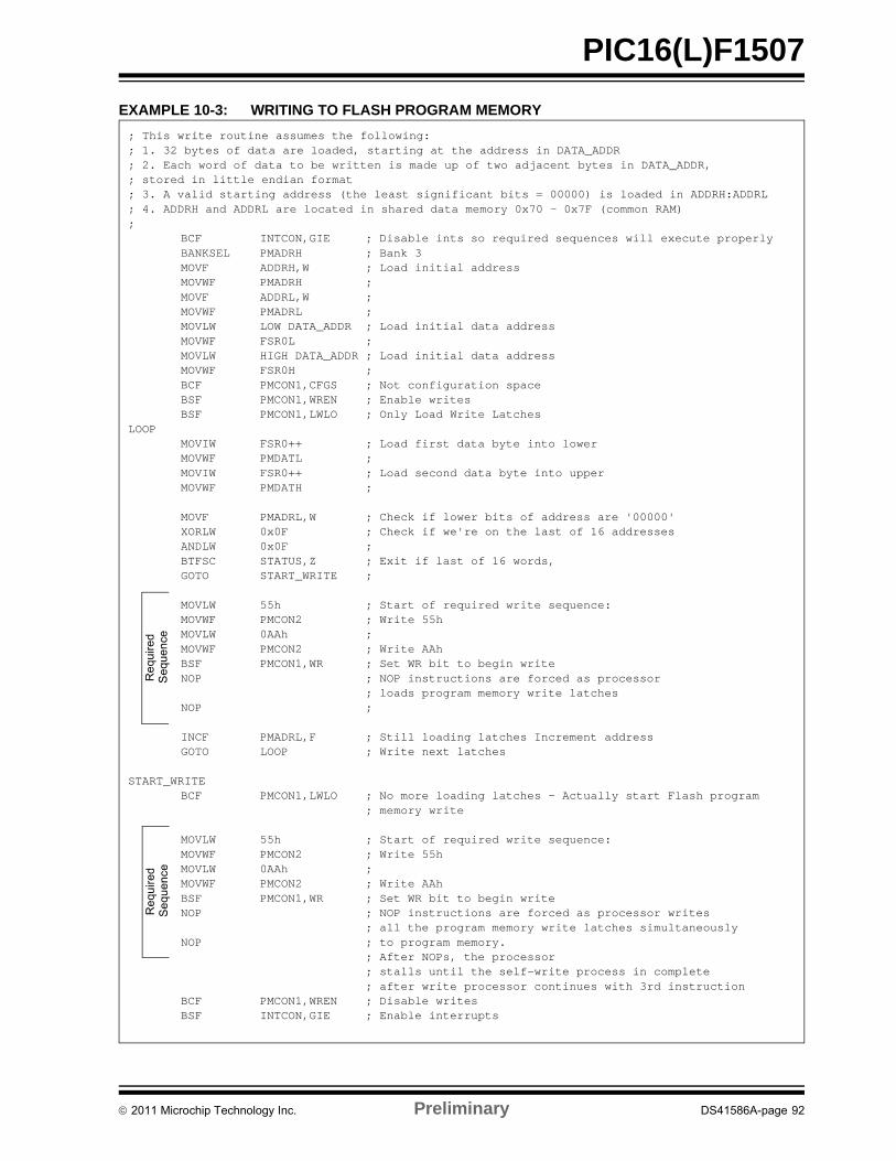
PIC16(L)F1507
EXAMPLE 10-3: WRITING TO FLASH PROGRAM MEMORY
; This write routine assumes the following:; 1. 32 bytes of data are loaded, starting at the address in DATA_ADDR; 2. Each word of data to be written is made up of two adjacent bytes in DATA_ADDR,; stored in little endian format; 3. A valid starting address (the least significant bits = 00000) is loaded in ADDRH:ADDRL; 4. ADDRH and ADDRL are located in shared data memory 0x70 - 0x7F (common RAM);
BCF INTCON,GIE ; Disable ints so required sequences will execute properlyBANKSEL PMADRH ; Bank 3MOVF ADDRH,W ; Load initial addressMOVWF PMADRH ;MOVF ADDRL,W ;MOVWF PMADRL ;MOVLW LOW DATA_ADDR ; Load initial data addressMOVWF FSR0L ;MOVLW HIGH DATA_ADDR ; Load initial data addressMOVWF FSR0H ;BCF PMCON1,CFGS ; Not configuration spaceBSF PMCON1,WREN ; Enable writesBSF PMCON1,LWLO ; Only Load Write Latches
LOOPMOVIW FSR0++ ; Load first data byte into lowerMOVWF PMDATL ;MOVIW FSR0++ ; Load second data byte into upperMOVWF PMDATH ;
MOVF PMADRL,W ; Check if lower bits of address are '00000'XORLW 0x0F ; Check if we're on the last of 16 addressesANDLW 0x0F ;BTFSC STATUS,Z ; Exit if last of 16 words,GOTO START_WRITE ;
MOVLW 55h ; Start of required write sequence:MOVWF PMCON2 ; Write 55hMOVLW 0AAh ;MOVWF PMCON2 ; Write AAhBSF PMCON1,WR ; Set WR bit to begin writeNOP ; NOP instructions are forced as processor
; loads program memory write latchesNOP ;
INCF PMADRL,F ; Still loading latches Increment addressGOTO LOOP ; Write next latches
START_WRITEBCF PMCON1,LWLO ; No more loading latches - Actually start Flash program
; memory write
MOVLW 55h ; Start of required write sequence:MOVWF PMCON2 ; Write 55hMOVLW 0AAh ;MOVWF PMCON2 ; Write AAhBSF PMCON1,WR ; Set WR bit to begin writeNOP ; NOP instructions are forced as processor writes
; all the program memory write latches simultaneouslyNOP ; to program memory.
; After NOPs, the processor; stalls until the self-write process in complete; after write processor continues with 3rd instruction
BCF PMCON1,WREN ; Disable writesBSF INTCON,GIE ; Enable interrupts
Re
qu
ire
dS
eq
ue
nce
Re
qu
ire
dS
eq
ue
nce
2011 Microchip Technology Inc. Preliminary DS41586A-page 92
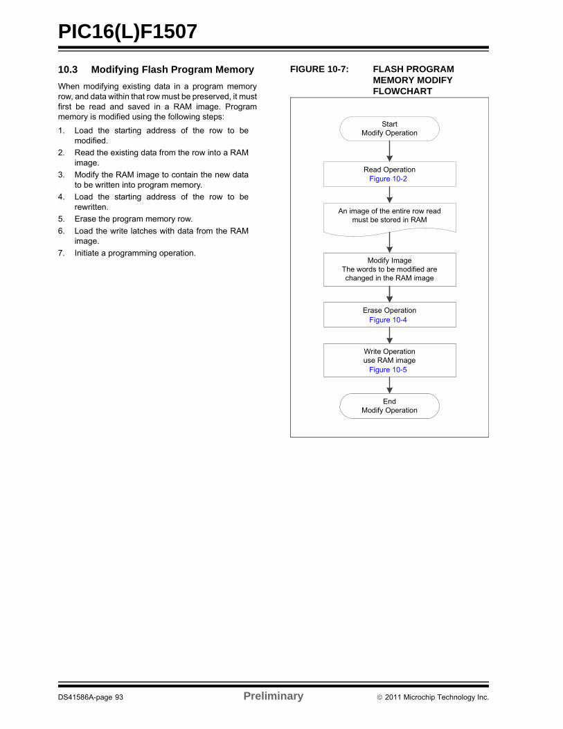
PIC16(L)F1507
10.3 Modifying Flash Program Memory
When modifying existing data in a program memoryrow, and data within that row must be preserved, it mustfirst be read and saved in a RAM image. Programmemory is modified using the following steps:
1. Load the starting address of the row to bemodified.
2. Read the existing data from the row into a RAMimage.
3. Modify the RAM image to contain the new datato be written into program memory.
4. Load the starting address of the row to berewritten.
5. Erase the program memory row.
6. Load the write latches with data from the RAMimage.
7. Initiate a programming operation.
FIGURE 10-7: FLASH PROGRAM MEMORY MODIFY FLOWCHART
Start Modify Operation
Read Operation(Figure x.x)
Erase Operation(Figure x.x)
Modify ImageThe words to be modified are changed in the RAM image
End Modify Operation
Write Operationuse RAM image
(Figure x.x)
An image of the entire row read must be stored in RAM
Figure 10-2
Figure 10-4
Figure 10-5
DS41586A-page 93 Preliminary 2011 Microchip Technology Inc.
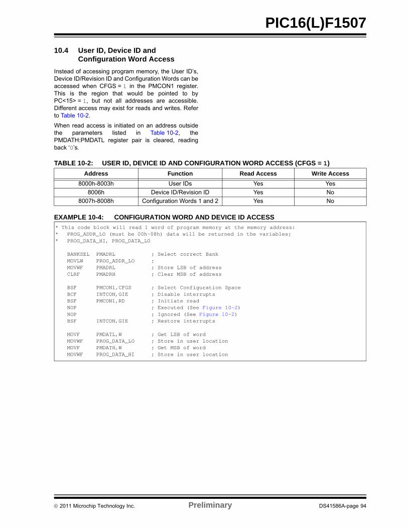
PIC16(L)F1507
10.4 User ID, Device ID and Configuration Word Access
Instead of accessing program memory, the User ID’s,Device ID/Revision ID and Configuration Words can beaccessed when CFGS = 1 in the PMCON1 register.This is the region that would be pointed to byPC<15> = 1, but not all addresses are accessible.Different access may exist for reads and writes. Referto Table 10-2.
When read access is initiated on an address outsidethe parameters listed in Table 10-2, thePMDATH:PMDATL register pair is cleared, readingback ‘0’s.
TABLE 10-2: USER ID, DEVICE ID AND CONFIGURATION WORD ACCESS (CFGS = 1)
EXAMPLE 10-4: CONFIGURATION WORD AND DEVICE ID ACCESS
Address Function Read Access Write Access
8000h-8003h User IDs Yes Yes
8006h Device ID/Revision ID Yes No
8007h-8008h Configuration Words 1 and 2 Yes No
* This code block will read 1 word of program memory at the memory address:* PROG_ADDR_LO (must be 00h-08h) data will be returned in the variables;* PROG_DATA_HI, PROG_DATA_LO
BANKSEL PMADRL ; Select correct BankMOVLW PROG_ADDR_LO ; MOVWF PMADRL ; Store LSB of addressCLRF PMADRH ; Clear MSB of address
BSF PMCON1,CFGS ; Select Configuration Space BCF INTCON,GIE ; Disable interruptsBSF PMCON1,RD ; Initiate readNOP ; Executed (See Figure 10-2)NOP ; Ignored (See Figure 10-2)BSF INTCON,GIE ; Restore interrupts
MOVF PMDATL,W ; Get LSB of wordMOVWF PROG_DATA_LO ; Store in user locationMOVF PMDATH,W ; Get MSB of wordMOVWF PROG_DATA_HI ; Store in user location
2011 Microchip Technology Inc. Preliminary DS41586A-page 94
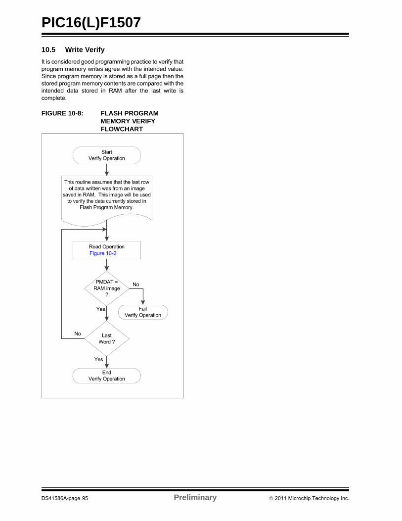
PIC16(L)F1507
10.5 Write Verify
It is considered good programming practice to verify thatprogram memory writes agree with the intended value.Since program memory is stored as a full page then thestored program memory contents are compared with theintended data stored in RAM after the last write iscomplete.
FIGURE 10-8: FLASH PROGRAM MEMORY VERIFY FLOWCHART
Start Verify Operation
Read Operation(Figure x.x)
End Verify Operation
This routine assumes that the last row of data written was from an image
saved in RAM. This image will be used to verify the data currently stored in
Flash Program Memory.
PMDAT = RAM image
?
LastWord ?
Fail Verify Operation
No
Yes
Yes
No
Figure 10-2
DS41586A-page 95 Preliminary 2011 Microchip Technology Inc.
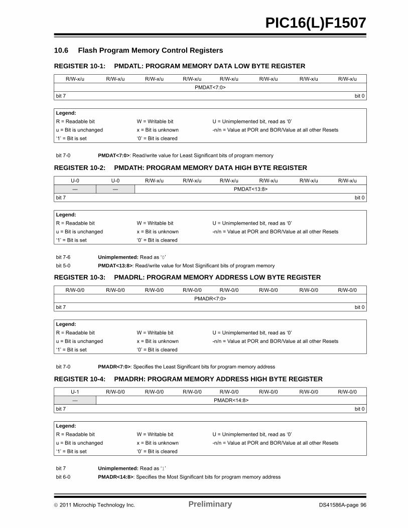
PIC16(L)F1507
10.6 Flash Program Memory Control Registers
REGISTER 10-1: PMDATL: PROGRAM MEMORY DATA LOW BYTE REGISTER
R/W-x/u R/W-x/u R/W-x/u R/W-x/u R/W-x/u R/W-x/u R/W-x/u R/W-x/u
PMDAT<7:0>
bit 7 bit 0
Legend:
R = Readable bit W = Writable bit U = Unimplemented bit, read as ‘0’
u = Bit is unchanged x = Bit is unknown -n/n = Value at POR and BOR/Value at all other Resets
‘1’ = Bit is set ‘0’ = Bit is cleared
bit 7-0 PMDAT<7:0>: Read/write value for Least Significant bits of program memory
REGISTER 10-2: PMDATH: PROGRAM MEMORY DATA HIGH BYTE REGISTER
U-0 U-0 R/W-x/u R/W-x/u R/W-x/u R/W-x/u R/W-x/u R/W-x/u
— — PMDAT<13:8>
bit 7 bit 0
Legend:
R = Readable bit W = Writable bit U = Unimplemented bit, read as ‘0’
u = Bit is unchanged x = Bit is unknown -n/n = Value at POR and BOR/Value at all other Resets
‘1’ = Bit is set ‘0’ = Bit is cleared
bit 7-6 Unimplemented: Read as ‘0’
bit 5-0 PMDAT<13:8>: Read/write value for Most Significant bits of program memory
REGISTER 10-3: PMADRL: PROGRAM MEMORY ADDRESS LOW BYTE REGISTER
R/W-0/0 R/W-0/0 R/W-0/0 R/W-0/0 R/W-0/0 R/W-0/0 R/W-0/0 R/W-0/0
PMADR<7:0>
bit 7 bit 0
Legend:
R = Readable bit W = Writable bit U = Unimplemented bit, read as ‘0’
u = Bit is unchanged x = Bit is unknown -n/n = Value at POR and BOR/Value at all other Resets
‘1’ = Bit is set ‘0’ = Bit is cleared
bit 7-0 PMADR<7:0>: Specifies the Least Significant bits for program memory address
REGISTER 10-4: PMADRH: PROGRAM MEMORY ADDRESS HIGH BYTE REGISTER
U-1 R/W-0/0 R/W-0/0 R/W-0/0 R/W-0/0 R/W-0/0 R/W-0/0 R/W-0/0
— PMADR<14:8>
bit 7 bit 0
Legend:
R = Readable bit W = Writable bit U = Unimplemented bit, read as ‘0’
u = Bit is unchanged x = Bit is unknown -n/n = Value at POR and BOR/Value at all other Resets
‘1’ = Bit is set ‘0’ = Bit is cleared
bit 7 Unimplemented: Read as ‘1’
bit 6-0 PMADR<14:8>: Specifies the Most Significant bits for program memory address
2011 Microchip Technology Inc. Preliminary DS41586A-page 96
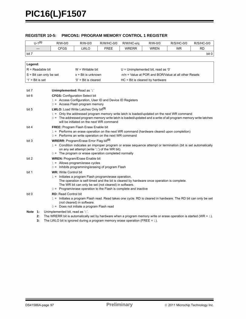
PIC16(L)F1507
REGISTER 10-5: PMCON1: PROGRAM MEMORY CONTROL 1 REGISTER
U-1(1) R/W-0/0 R/W-0/0 R/W/HC-0/0 R/W/HC-x/q R/W-0/0 R/S/HC-0/0 R/S/HC-0/0
— CFGS LWLO FREE WRERR WREN WR RD
bit 7 bit 0
Legend:
R = Readable bit W = Writable bit U = Unimplemented bit, read as ‘0’
S = Bit can only be set x = Bit is unknown -n/n = Value at POR and BOR/Value at all other Resets
‘1’ = Bit is set ‘0’ = Bit is cleared HC = Bit is cleared by hardware
bit 7 Unimplemented: Read as ‘1’
bit 6 CFGS: Configuration Select bit1 = Access Configuration, User ID and Device ID Registers0 = Access Flash program memory
bit 5 LWLO: Load Write Latches Only bit(3)
1 = Only the addressed program memory write latch is loaded/updated on the next WR command0 = The addressed program memory write latch is loaded/updated and a write of all program memory write latches
will be initiated on the next WR command
bit 4 FREE: Program Flash Erase Enable bit 1 = Performs an erase operation on the next WR command (hardware cleared upon completion)0 = Performs an write operation on the next WR command
bit 3 WRERR: Program/Erase Error Flag bit(2)
1 = Condition indicates an improper program or erase sequence attempt or termination (bit is set automaticallyon any set attempt (write ‘1’) of the WR bit).
0 = The program or erase operation completed normally
bit 2 WREN: Program/Erase Enable bit1 = Allows program/erase cycles0 = Inhibits programming/erasing of program Flash
bit 1 WR: Write Control bit1 = Initiates a program Flash program/erase operation.
The operation is self-timed and the bit is cleared by hardware once operation is complete. The WR bit can only be set (not cleared) in software.
0 = Program/erase operation to the Flash is complete and inactive
bit 0 RD: Read Control bit1 = Initiates a program Flash read. Read takes one cycle. RD is cleared in hardware. The RD bit can only be set
(not cleared) in software.0 = Does not initiate a program Flash read
Note 1: Unimplemented bit, read as ‘1’.2: The WRERR bit is automatically set by hardware when a program memory write or erase operation is started (WR = 1).3: The LWLO bit is ignored during a program memory erase operation (FREE = 1).
DS41586A-page 97 Preliminary 2011 Microchip Technology Inc.
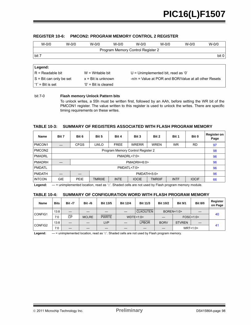
PIC16(L)F1507
TABLE 10-3: SUMMARY OF REGISTERS ASSOCIATED WITH FLASH PROGRAM MEMORY
TABLE 10-4: SUMMARY OF CONFIGURATION WORD WITH FLASH PROGRAM MEMORY
REGISTER 10-6: PMCON2: PROGRAM MEMORY CONTROL 2 REGISTER
W-0/0 W-0/0 W-0/0 W-0/0 W-0/0 W-0/0 W-0/0 W-0/0
Program Memory Control Register 2
bit 7 bit 0
Legend:
R = Readable bit W = Writable bit U = Unimplemented bit, read as ‘0’
S = Bit can only be set x = Bit is unknown -n/n = Value at POR and BOR/Value at all other Resets
‘1’ = Bit is set ‘0’ = Bit is cleared
bit 7-0 Flash memory Unlock Pattern bits
To unlock writes, a 55h must be written first, followed by an AAh, before setting the WR bit of thePMCON1 register. The value written to this register is used to unlock the writes. There are specifictiming requirements on these writes.
Name Bit 7 Bit 6 Bit 5 Bit 4 Bit 3 Bit 2 Bit 1 Bit 0Register on
Page
PMCON1 — CFGS LWLO FREE WRERR WREN WR RD 97
PMCON2 Program Memory Control Register 2 98
PMADRL PMADRL<7:0> 96
PMADRH — PMADRH<6:0> 96
PMDATL PMDATL<7:0> 96
PMDATH — — PMDATH<5:0> 96
INTCON GIE PEIE TMR0IE INTE IOCIE TMR0IF INTF IOCIF 66
Legend: — = unimplemented location, read as ‘0’. Shaded cells are not used by Flash program memory module.
Name Bits Bit -/7 Bit -/6 Bit 13/5 Bit 12/4 Bit 11/3 Bit 10/2 Bit 9/1 Bit 8/0Register on Page
CONFIG113:8 — — — — CLKOUTEN BOREN<1:0> —
407:0 CP MCLRE PWRTE WDTE<1:0> — FOSC<1:0>
CONFIG213:8 — — LVP — LPBOR BORV STVREN —
417:0 — — — — — — WRT<1:0>
Legend: — = unimplemented location, read as ‘0’. Shaded cells are not used by Flash program memory.
2011 Microchip Technology Inc. Preliminary DS41586A-page 98
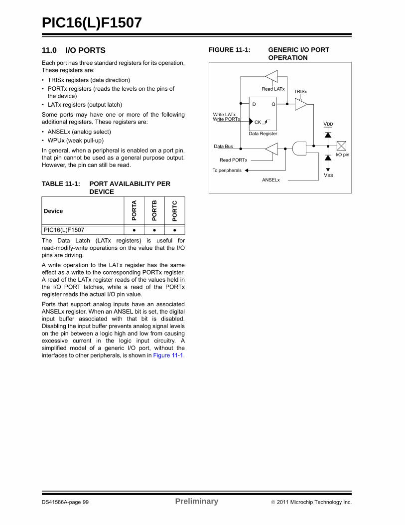
PIC16(L)F1507
11.0 I/O PORTS
Each port has three standard registers for its operation.These registers are:
• TRISx registers (data direction)
• PORTx registers (reads the levels on the pins of the device)
• LATx registers (output latch)
Some ports may have one or more of the followingadditional registers. These registers are:
• ANSELx (analog select)
• WPUx (weak pull-up)
In general, when a peripheral is enabled on a port pin,that pin cannot be used as a general purpose output.However, the pin can still be read.
The Data Latch (LATx registers) is useful forread-modify-write operations on the value that the I/Opins are driving.
A write operation to the LATx register has the sameeffect as a write to the corresponding PORTx register.A read of the LATx register reads of the values held inthe I/O PORT latches, while a read of the PORTxregister reads the actual I/O pin value.
Ports that support analog inputs have an associatedANSELx register. When an ANSEL bit is set, the digitalinput buffer associated with that bit is disabled.Disabling the input buffer prevents analog signal levelson the pin between a logic high and low from causingexcessive current in the logic input circuitry. Asimplified model of a generic I/O port, without theinterfaces to other peripherals, is shown in Figure 11-1.
FIGURE 11-1: GENERIC I/O PORT OPERATION
TABLE 11-1: PORT AVAILABILITY PER DEVICE
Device
PO
RTA
PO
RT
B
PO
RT
C
PIC16(L)F1507 ● ● ●
QD
CK
Write LATx
Data Register
I/O pinRead PORTx
Write PORTx
TRISxRead LATx
Data Bus
To peripherals
ANSELx
VDD
VSS
DS41586A-page 99 Preliminary 2011 Microchip Technology Inc.
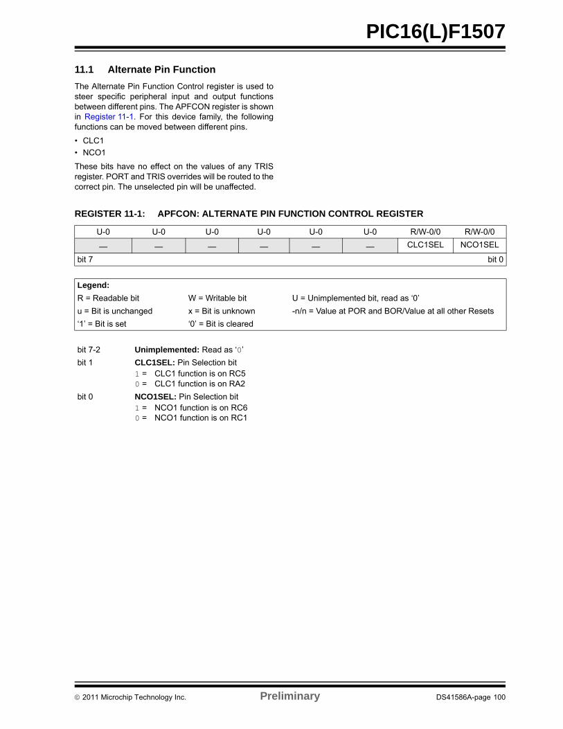
PIC16(L)F1507
11.1 Alternate Pin Function
The Alternate Pin Function Control register is used tosteer specific peripheral input and output functionsbetween different pins. The APFCON register is shownin Register 11-1. For this device family, the followingfunctions can be moved between different pins.
• CLC1
• NCO1
These bits have no effect on the values of any TRISregister. PORT and TRIS overrides will be routed to thecorrect pin. The unselected pin will be unaffected.
REGISTER 11-1: APFCON: ALTERNATE PIN FUNCTION CONTROL REGISTER
U-0 U-0 U-0 U-0 U-0 U-0 R/W-0/0 R/W-0/0
— — — — — — CLC1SEL NCO1SEL
bit 7 bit 0
Legend:
R = Readable bit W = Writable bit U = Unimplemented bit, read as ‘0’
u = Bit is unchanged x = Bit is unknown -n/n = Value at POR and BOR/Value at all other Resets
‘1’ = Bit is set ‘0’ = Bit is cleared
bit 7-2 Unimplemented: Read as ‘0’
bit 1 CLC1SEL: Pin Selection bit1 = CLC1 function is on RC50 = CLC1 function is on RA2
bit 0 NCO1SEL: Pin Selection bit1 = NCO1 function is on RC60 = NCO1 function is on RC1
2011 Microchip Technology Inc. Preliminary DS41586A-page 100
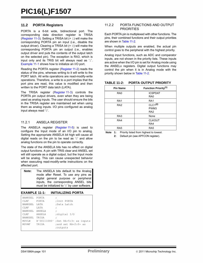
PIC16(L)F1507
11.2 PORTA Registers
PORTA is a 6-bit wide, bidirectional port. Thecorresponding data direction register is TRISA(Register 11-3). Setting a TRISA bit (= 1) will make thecorresponding PORTA pin an input (i.e., disable theoutput driver). Clearing a TRISA bit (= 0) will make thecorresponding PORTA pin an output (i.e., enablesoutput driver and puts the contents of the output latchon the selected pin). The exception is RA3, which isinput only and its TRIS bit will always read as ‘1’.Example 11-1 shows how to initialize an I/O port.
Reading the PORTA register (Register 11-2) reads thestatus of the pins, whereas writing to it will write to thePORT latch. All write operations are read-modify-writeoperations. Therefore, a write to a port implies that theport pins are read, this value is modified and thenwritten to the PORT data latch (LATA).
The TRISA register (Register 11-3) controls thePORTA pin output drivers, even when they are beingused as analog inputs. The user should ensure the bitsin the TRISA register are maintained set when usingthem as analog inputs. I/O pins configured as analoginput always read ‘0’.
11.2.1 ANSELA REGISTER
The ANSELA register (Register 11-5) is used toconfigure the Input mode of an I/O pin to analog.Setting the appropriate ANSELA bit high will cause alldigital reads on the pin to be read as ‘0’ and allowanalog functions on the pin to operate correctly.
The state of the ANSELA bits has no effect on digitaloutput functions. A pin with TRIS clear and ANSEL setwill still operate as a digital output, but the Input modewill be analog. This can cause unexpected behaviorwhen executing read-modify-write instructions on theaffected port.
EXAMPLE 11-1: INITIALIZING PORTA
11.2.2 PORTA FUNCTIONS AND OUTPUT PRIORITIES
Each PORTA pin is multiplexed with other functions. Thepins, their combined functions and their output prioritiesare shown in Table 11-2.
When multiple outputs are enabled, the actual pincontrol goes to the peripheral with the highest priority.
Analog input functions, such as ADC and comparatorinputs, are not shown in the priority lists. These inputsare active when the I/O pin is set for Analog mode usingthe ANSELx registers. Digital output functions maycontrol the pin when it is in Analog mode with thepriority shown below in Table 11-2.
Note: The ANSELA bits default to the Analogmode after Reset. To use any pins asdigital general purpose or peripheralinputs, the corresponding ANSEL bitsmust be initialized to ‘0’ by user software.
BANKSEL PORTA ;CLRF PORTA ;Init PORTABANKSEL LATA ;Data LatchCLRF LATA ;BANKSEL ANSELA ;CLRF ANSELA ;digital I/OBANKSEL TRISA ;MOVLW B'00111000' ;Set RA<5:3> as inputsMOVWF TRISA ;and set RA<2:0> as
;outputs
TABLE 11-2: PORTA OUTPUT PRIORITY
Pin Name Function Priority(1)
RA0 ICSPDATRA0
RA1 RA1
RA2 CLC1(2)
PWM3RA2
RA3 None
RA4 CLKOUTRA4
RA5 RA5
Note 1: Priority listed from highest to lowest.2: Default pin (see APFCON register).
DS41586A-page 101 Preliminary 2011 Microchip Technology Inc.
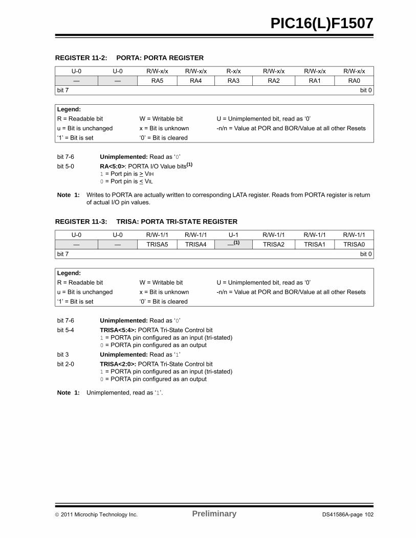
PIC16(L)F1507
REGISTER 11-2: PORTA: PORTA REGISTER
U-0 U-0 R/W-x/x R/W-x/x R-x/x R/W-x/x R/W-x/x R/W-x/x
— — RA5 RA4 RA3 RA2 RA1 RA0
bit 7 bit 0
Legend:
R = Readable bit W = Writable bit U = Unimplemented bit, read as ‘0’
u = Bit is unchanged x = Bit is unknown -n/n = Value at POR and BOR/Value at all other Resets
‘1’ = Bit is set ‘0’ = Bit is cleared
bit 7-6 Unimplemented: Read as ‘0’
bit 5-0 RA<5:0>: PORTA I/O Value bits(1)
1 = Port pin is > VIH
0 = Port pin is < VIL
Note 1: Writes to PORTA are actually written to corresponding LATA register. Reads from PORTA register is return of actual I/O pin values.
REGISTER 11-3: TRISA: PORTA TRI-STATE REGISTER
U-0 U-0 R/W-1/1 R/W-1/1 U-1 R/W-1/1 R/W-1/1 R/W-1/1
— — TRISA5 TRISA4 —(1) TRISA2 TRISA1 TRISA0
bit 7 bit 0
Legend:
R = Readable bit W = Writable bit U = Unimplemented bit, read as ‘0’
u = Bit is unchanged x = Bit is unknown -n/n = Value at POR and BOR/Value at all other Resets
‘1’ = Bit is set ‘0’ = Bit is cleared
bit 7-6 Unimplemented: Read as ‘0’
bit 5-4 TRISA<5:4>: PORTA Tri-State Control bit1 = PORTA pin configured as an input (tri-stated)0 = PORTA pin configured as an output
bit 3 Unimplemented: Read as ‘1’
bit 2-0 TRISA<2:0>: PORTA Tri-State Control bit1 = PORTA pin configured as an input (tri-stated)0 = PORTA pin configured as an output
Note 1: Unimplemented, read as ‘1’.
2011 Microchip Technology Inc. Preliminary DS41586A-page 102
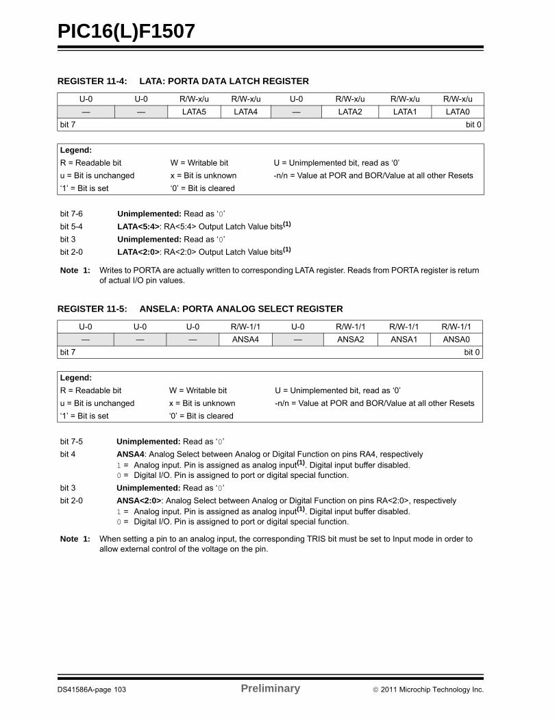
PIC16(L)F1507
REGISTER 11-4: LATA: PORTA DATA LATCH REGISTER
U-0 U-0 R/W-x/u R/W-x/u U-0 R/W-x/u R/W-x/u R/W-x/u
— — LATA5 LATA4 — LATA2 LATA1 LATA0
bit 7 bit 0
Legend:
R = Readable bit W = Writable bit U = Unimplemented bit, read as ‘0’
u = Bit is unchanged x = Bit is unknown -n/n = Value at POR and BOR/Value at all other Resets
‘1’ = Bit is set ‘0’ = Bit is cleared
bit 7-6 Unimplemented: Read as ‘0’
bit 5-4 LATA<5:4>: RA<5:4> Output Latch Value bits(1)
bit 3 Unimplemented: Read as ‘0’
bit 2-0 LATA<2:0>: RA<2:0> Output Latch Value bits(1)
Note 1: Writes to PORTA are actually written to corresponding LATA register. Reads from PORTA register is return of actual I/O pin values.
REGISTER 11-5: ANSELA: PORTA ANALOG SELECT REGISTER
U-0 U-0 U-0 R/W-1/1 U-0 R/W-1/1 R/W-1/1 R/W-1/1
— — — ANSA4 — ANSA2 ANSA1 ANSA0
bit 7 bit 0
Legend:
R = Readable bit W = Writable bit U = Unimplemented bit, read as ‘0’
u = Bit is unchanged x = Bit is unknown -n/n = Value at POR and BOR/Value at all other Resets
‘1’ = Bit is set ‘0’ = Bit is cleared
bit 7-5 Unimplemented: Read as ‘0’
bit 4 ANSA4: Analog Select between Analog or Digital Function on pins RA4, respectively1 = Analog input. Pin is assigned as analog input(1). Digital input buffer disabled.0 = Digital I/O. Pin is assigned to port or digital special function.
bit 3 Unimplemented: Read as ‘0’
bit 2-0 ANSA<2:0>: Analog Select between Analog or Digital Function on pins RA<2:0>, respectively1 = Analog input. Pin is assigned as analog input(1). Digital input buffer disabled.0 = Digital I/O. Pin is assigned to port or digital special function.
Note 1: When setting a pin to an analog input, the corresponding TRIS bit must be set to Input mode in order to allow external control of the voltage on the pin.
DS41586A-page 103 Preliminary 2011 Microchip Technology Inc.
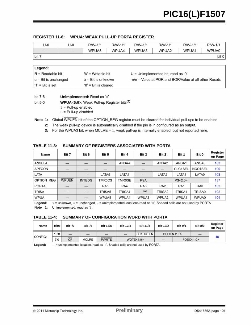
PIC16(L)F1507
TABLE 11-3: SUMMARY OF REGISTERS ASSOCIATED WITH PORTA
TABLE 11-4: SUMMARY OF CONFIGURATION WORD WITH PORTA
REGISTER 11-6: WPUA: WEAK PULL-UP PORTA REGISTER
U-0 U-0 R/W-1/1 R/W-1/1 R/W-1/1 R/W-1/1 R/W-1/1 R/W-1/1
— — WPUA5 WPUA4 WPUA3 WPUA2 WPUA1 WPUA0
bit 7 bit 0
Legend:
R = Readable bit W = Writable bit U = Unimplemented bit, read as ‘0’
u = Bit is unchanged x = Bit is unknown -n/n = Value at POR and BOR/Value at all other Resets
‘1’ = Bit is set ‘0’ = Bit is cleared
bit 7-6 Unimplemented: Read as ‘0’
bit 5-0 WPUA<5:0>: Weak Pull-up Register bits(3)
1 = Pull-up enabled0 = Pull-up disabled
Note 1: Global WPUEN bit of the OPTION_REG register must be cleared for individual pull-ups to be enabled.
2: The weak pull-up device is automatically disabled if the pin is in configured as an output.
3: For the WPUA3 bit, when MCLRE = 1, weak pull-up is internally enabled, but not reported here.
Name Bit 7 Bit 6 Bit 5 Bit 4 Bit 3 Bit 2 Bit 1 Bit 0Register on Page
ANSELA — — — ANSA4 — ANSA2 ANSA1 ANSA0 103
APFCON — — — — — — CLC1SEL NCO1SEL 100
LATA — — LATA5 LATA4 — LATA2 LATA1 LATA0 103
OPTION_REG WPUEN INTEDG TMR0CS TMR0SE PSA PS<2:0> 137
PORTA — — RA5 RA4 RA3 RA2 RA1 RA0 102
TRISA — — TRISA5 TRISA4 —(1) TRISA2 TRISA1 TRISA0 102
WPUA — — WPUA5 WPUA4 WPUA3 WPUA2 WPUA1 WPUA0 104
Legend: x = unknown, u = unchanged, – = unimplemented locations read as ‘0’. Shaded cells are not used by PORTA.Note 1: Unimplemented, read as ‘1’.
Name Bits Bit -/7 Bit -/6 Bit 13/5 Bit 12/4 Bit 11/3 Bit 10/2 Bit 9/1 Bit 8/0Register on Page
CONFIG113:8 — — — — CLKOUTEN BOREN<1:0> —
407:0 CP MCLRE PWRTE WDTE<1:0> — FOSC<1:0>
Legend: — = unimplemented location, read as ‘0’. Shaded cells are not used by PORTA.
2011 Microchip Technology Inc. Preliminary DS41586A-page 104
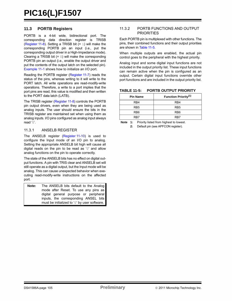
PIC16(L)F1507
11.3 PORTB Registers
PORTB is a 4-bit wide, bidirectional port. Thecorresponding data direction register is TRISB(Register 11-8). Setting a TRISB bit (= 1) will make thecorresponding PORTB pin an input (i.e., put thecorresponding output driver in a High-Impedance mode).Clearing a TRISB bit (= 0) will make the correspondingPORTB pin an output (i.e., enable the output driver andput the contents of the output latch on the selected pin).Example 11-1 shows how to initialize an I/O port.
Reading the PORTB register (Register 11-7) reads thestatus of the pins, whereas writing to it will write to thePORT latch. All write operations are read-modify-writeoperations. Therefore, a write to a port implies that theport pins are read, this value is modified and then writtento the PORT data latch (LATB).
The TRISB register (Register 11-8) controls the PORTBpin output drivers, even when they are being used asanalog inputs. The user should ensure the bits in theTRISB register are maintained set when using them asanalog inputs. I/O pins configured as analog input alwaysread ‘0’.
11.3.1 ANSELB REGISTER
The ANSELB register (Register 11-10) is used toconfigure the Input mode of an I/O pin to analog.Setting the appropriate ANSELB bit high will cause alldigital reads on the pin to be read as ‘0’ and allowanalog functions on the pin to operate correctly.
The state of the ANSELB bits has no effect on digital out-put functions. A pin with TRIS clear and ANSELB set willstill operate as a digital output, but the Input mode will beanalog. This can cause unexpected behavior when exe-cuting read-modify-write instructions on the affectedport.
11.3.2 PORTB FUNCTIONS AND OUTPUT PRIORITIES
Each PORTB pin is multiplexed with other functions. Thepins, their combined functions and their output prioritiesare shown in Table 11-5.
When multiple outputs are enabled, the actual pincontrol goes to the peripheral with the highest priority.
Analog input and some digital input functions are notincluded in the output priority list. These input functionscan remain active when the pin is configured as anoutput. Certain digital input functions override otherport functions and are included in the output priority list.
Note: The ANSELB bits default to the Analogmode after Reset. To use any pins asdigital general purpose or peripheralinputs, the corresponding ANSEL bitsmust be initialized to ‘0’ by user software.
TABLE 11-5: PORTB OUTPUT PRIORITY
Pin Name Function Priority(1)
RB4 RB4
RB5 RB5
RB6 RB6
RB7 RB7
Note 1: Priority listed from highest to lowest.2: Default pin (see APFCON register).
DS41586A-page 105 Preliminary 2011 Microchip Technology Inc.
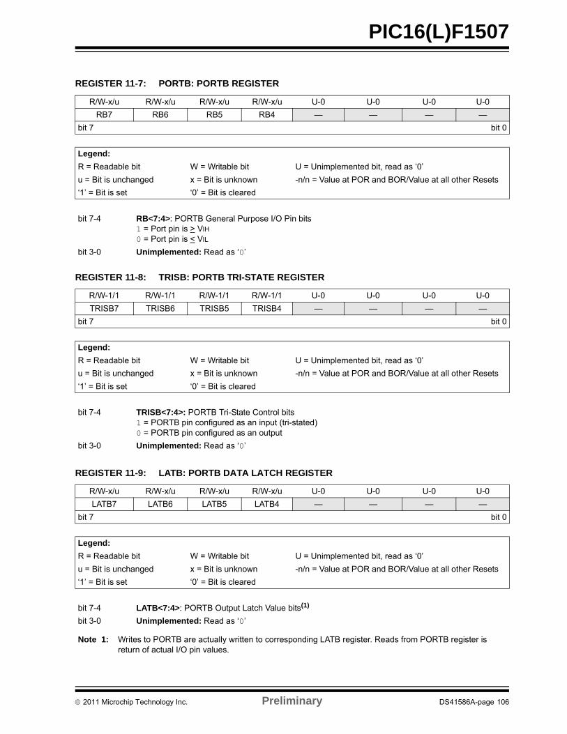
PIC16(L)F1507
REGISTER 11-7: PORTB: PORTB REGISTER
R/W-x/u R/W-x/u R/W-x/u R/W-x/u U-0 U-0 U-0 U-0
RB7 RB6 RB5 RB4 — — — —
bit 7 bit 0
Legend:
R = Readable bit W = Writable bit U = Unimplemented bit, read as ‘0’
u = Bit is unchanged x = Bit is unknown -n/n = Value at POR and BOR/Value at all other Resets
‘1’ = Bit is set ‘0’ = Bit is cleared
bit 7-4 RB<7:4>: PORTB General Purpose I/O Pin bits1 = Port pin is > VIH
0 = Port pin is < VIL
bit 3-0 Unimplemented: Read as ‘0’
REGISTER 11-8: TRISB: PORTB TRI-STATE REGISTER
R/W-1/1 R/W-1/1 R/W-1/1 R/W-1/1 U-0 U-0 U-0 U-0
TRISB7 TRISB6 TRISB5 TRISB4 — — — —
bit 7 bit 0
Legend:
R = Readable bit W = Writable bit U = Unimplemented bit, read as ‘0’
u = Bit is unchanged x = Bit is unknown -n/n = Value at POR and BOR/Value at all other Resets
‘1’ = Bit is set ‘0’ = Bit is cleared
bit 7-4 TRISB<7:4>: PORTB Tri-State Control bits1 = PORTB pin configured as an input (tri-stated)0 = PORTB pin configured as an output
bit 3-0 Unimplemented: Read as ‘0’
REGISTER 11-9: LATB: PORTB DATA LATCH REGISTER
R/W-x/u R/W-x/u R/W-x/u R/W-x/u U-0 U-0 U-0 U-0
LATB7 LATB6 LATB5 LATB4 — — — —
bit 7 bit 0
Legend:
R = Readable bit W = Writable bit U = Unimplemented bit, read as ‘0’
u = Bit is unchanged x = Bit is unknown -n/n = Value at POR and BOR/Value at all other Resets
‘1’ = Bit is set ‘0’ = Bit is cleared
bit 7-4 LATB<7:4>: PORTB Output Latch Value bits(1)
bit 3-0 Unimplemented: Read as ‘0’
Note 1: Writes to PORTB are actually written to corresponding LATB register. Reads from PORTB register is return of actual I/O pin values.
2011 Microchip Technology Inc. Preliminary DS41586A-page 106
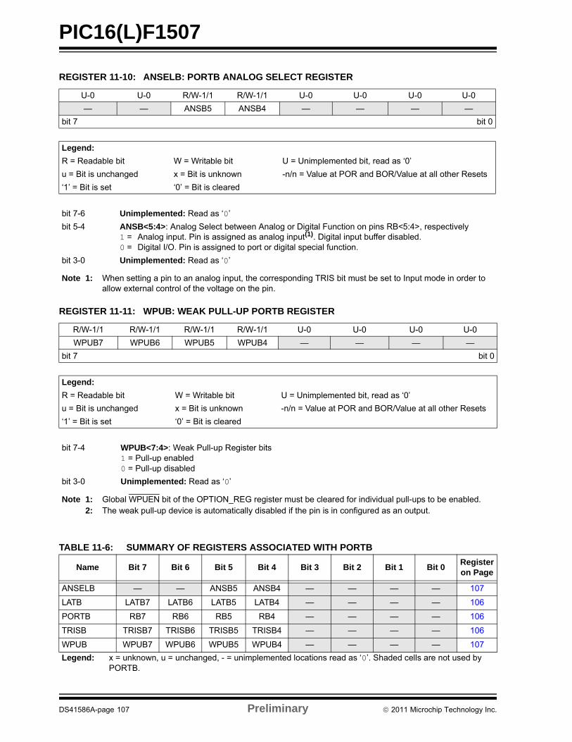
PIC16(L)F1507
TABLE 11-6: SUMMARY OF REGISTERS ASSOCIATED WITH PORTB
REGISTER 11-10: ANSELB: PORTB ANALOG SELECT REGISTER
U-0 U-0 R/W-1/1 R/W-1/1 U-0 U-0 U-0 U-0
— — ANSB5 ANSB4 — — — —
bit 7 bit 0
Legend:
R = Readable bit W = Writable bit U = Unimplemented bit, read as ‘0’
u = Bit is unchanged x = Bit is unknown -n/n = Value at POR and BOR/Value at all other Resets
‘1’ = Bit is set ‘0’ = Bit is cleared
bit 7-6 Unimplemented: Read as ‘0’
bit 5-4 ANSB<5:4>: Analog Select between Analog or Digital Function on pins RB<5:4>, respectively1 = Analog input. Pin is assigned as analog input(1). Digital input buffer disabled.0 = Digital I/O. Pin is assigned to port or digital special function.
bit 3-0 Unimplemented: Read as ‘0’
Note 1: When setting a pin to an analog input, the corresponding TRIS bit must be set to Input mode in order to allow external control of the voltage on the pin.
REGISTER 11-11: WPUB: WEAK PULL-UP PORTB REGISTER
R/W-1/1 R/W-1/1 R/W-1/1 R/W-1/1 U-0 U-0 U-0 U-0
WPUB7 WPUB6 WPUB5 WPUB4 — — — —
bit 7 bit 0
Legend:
R = Readable bit W = Writable bit U = Unimplemented bit, read as ‘0’
u = Bit is unchanged x = Bit is unknown -n/n = Value at POR and BOR/Value at all other Resets
‘1’ = Bit is set ‘0’ = Bit is cleared
bit 7-4 WPUB<7:4>: Weak Pull-up Register bits1 = Pull-up enabled0 = Pull-up disabled
bit 3-0 Unimplemented: Read as ‘0’
Note 1: Global WPUEN bit of the OPTION_REG register must be cleared for individual pull-ups to be enabled.2: The weak pull-up device is automatically disabled if the pin is in configured as an output.
Name Bit 7 Bit 6 Bit 5 Bit 4 Bit 3 Bit 2 Bit 1 Bit 0Register on Page
ANSELB — — ANSB5 ANSB4 — — — — 107
LATB LATB7 LATB6 LATB5 LATB4 — — — — 106
PORTB RB7 RB6 RB5 RB4 — — — — 106
TRISB TRISB7 TRISB6 TRISB5 TRISB4 — — — — 106
WPUB WPUB7 WPUB6 WPUB5 WPUB4 — — — — 107
Legend: x = unknown, u = unchanged, - = unimplemented locations read as ‘0’. Shaded cells are not used by PORTB.
DS41586A-page 107 Preliminary 2011 Microchip Technology Inc.
PIC16(L)F1507
11.4 PORTC Registers
PORTC is an 8-bit wide, bidirectional port. Thecorresponding data direction register is TRISC(Register 11-8). Setting a TRISC bit (= 1) will make thecorresponding PORTC pin an input (i.e., put thecorresponding output driver in a High-Impedancemode). Clearing a TRISC bit (= 0) will make thecorresponding PORTC pin an output (i.e., enable theoutput driver and put the contents of the output latchon the selected pin). Example 11-1 shows how toinitialize an I/O port.
Reading the PORTC register (Register 11-7) reads thestatus of the pins, whereas writing to it will write to thePORT latch. All write operations are read-modify-writeoperations. Therefore, a write to a port implies that theport pins are read, this value is modified and then writtento the PORT data latch (LATC).
The TRISC register (Register 11-8) controls the PORTCpin output drivers, even when they are being used asanalog inputs. The user should ensure the bits in theTRISC register are maintained set when using them asanalog inputs. I/O pins configured as analog input alwaysread ‘0’.
11.4.1 ANSELC REGISTER
The ANSELC register (Register 11-10) is used toconfigure the Input mode of an I/O pin to analog.Setting the appropriate ANSELC bit high will cause alldigital reads on the pin to be read as ‘0’ and allowanalog functions on the pin to operate correctly.
The state of the ANSELC bits has no effect on digital out-put functions. A pin with TRIS clear and ANSELC set willstill operate as a digital output, but the Input mode will beanalog. This can cause unexpected behavior when exe-cuting read-modify-write instructions on the affectedport.
11.4.2 PORTC FUNCTIONS AND OUTPUT PRIORITIES
Each PORTC pin is multiplexed with other functions. Thepins, their combined functions and their output prioritiesare shown in Table 11-7.
When multiple outputs are enabled, the actual pincontrol goes to the peripheral with the highest priority.
Analog input and some digital input functions are notincluded in the output priority list. These input functionscan remain active when the pin is configured as anoutput. Certain digital input functions override otherport functions and are included in the output priority list.
Note: The ANSELC bits default to the Analogmode after Reset. To use any pins asdigital general purpose or peripheralinputs, the corresponding ANSEL bitsmust be initialized to ‘0’ by user software.
TABLE 11-7: PORTC OUTPUT PRIORITY
Pin Name Function Priority(1)
RC0 CLC2RC0
RC1 NCO1(2)
PWM4RC1
RC2 RC2
RC3 PWM2RC3
RC4 CWG1BRC4
RC5 CWG1ACLC1(3)
PWM1RC5
RC6 NCO1(3)
RC6
RC7 RC7
Note 1: Priority listed from highest to lowest.2: Default pin (see APFCON register).3: Alternate pin (see APFCON register).
2011 Microchip Technology Inc. Preliminary DS41586A-page 108
PIC16(L)F1507
REGISTER 11-12: PORTC: PORTC REGISTER
R/W-x/u R/W-x/u R/W-x/u R/W-x/u R/W-x/u R/W-x/u R/W-x/u R/W-x/u
RC7 RC6 RC5 RC4 RC3 RC2 RC1 RC0
bit 7 bit 0
Legend:
R = Readable bit W = Writable bit U = Unimplemented bit, read as ‘0’
u = Bit is unchanged x = Bit is unknown -n/n = Value at POR and BOR/Value at all other Resets
‘1’ = Bit is set ‘0’ = Bit is cleared
bit 7-0 RC<7:0>: PORTC General Purpose I/O Pin bits1 = Port pin is > VIH
0 = Port pin is < VIL
REGISTER 11-13: TRISC: PORTC TRI-STATE REGISTER
R/W-1/1 R/W-1/1 R/W-1/1 R/W-1/1 R/W-1/1 R/W-1/1 R/W-1/1 R/W-1/1
TRISC7 TRISC6 TRISC5 TRISC4 TRISC3 TRISC2 TRISC1 TRISC0
bit 7 bit 0
Legend:
R = Readable bit W = Writable bit U = Unimplemented bit, read as ‘0’
u = Bit is unchanged x = Bit is unknown -n/n = Value at POR and BOR/Value at all other Resets
‘1’ = Bit is set ‘0’ = Bit is cleared
bit 7-0 TRISC<7:0>: PORTC Tri-State Control bits1 = PORTC pin configured as an input (tri-stated)0 = PORTC pin configured as an output
REGISTER 11-14: LATC: PORTC DATA LATCH REGISTER
R/W-x/u R/W-x/u R/W-x/u R/W-x/u R/W-x/u R/W-x/u R/W-x/u R/W-x/u
LATC7 LATC6 LATC5 LATC4 LATC3 LATC2 LATC1 LATC0
bit 7 bit 0
Legend:
R = Readable bit W = Writable bit U = Unimplemented bit, read as ‘0’
u = Bit is unchanged x = Bit is unknown -n/n = Value at POR and BOR/Value at all other Resets
‘1’ = Bit is set ‘0’ = Bit is cleared
bit 7-0 LATC<7:0>: PORTC Output Latch Value bits(1)
Note 1: Writes to PORTC are actually written to corresponding LATC register. Reads from PORTC register is return of actual I/O pin values.
DS41586A-page 109 Preliminary 2011 Microchip Technology Inc.
PIC16(L)F1507
TABLE 11-8: SUMMARY OF REGISTERS ASSOCIATED WITH PORTC
REGISTER 11-15: ANSELC: PORTC ANALOG SELECT REGISTER
R/W-1/1 R/W-1/1 U-0 U-0 R/W-1/1 R/W-1/1 R/W-1/1 R/W-1/1
ANSC7 ANSC6 — — ANSC3 ANSC2 ANSC1 ANSC0
bit 7 bit 0
Legend:
R = Readable bit W = Writable bit U = Unimplemented bit, read as ‘0’
u = Bit is unchanged x = Bit is unknown -n/n = Value at POR and BOR/Value at all other Resets
‘1’ = Bit is set ‘0’ = Bit is cleared
bit 7-6 ANSC<7:6>: Analog Select between Analog or Digital Function on pins RC<3:0>, respectively1 = Analog input. Pin is assigned as analog input(1). Digital input buffer disabled.0 = Digital I/O. Pin is assigned to port or digital special function.
bit 5-4 Unimplemented: Read as ‘0’
bit 3-0 ANSC<3:0>: Analog Select between Analog or Digital Function on pins RC<3:0>, respectively1 = Analog input. Pin is assigned as analog input(1). Digital input buffer disabled.0 = Digital I/O. Pin is assigned to port or digital special function.
Note 1: When setting a pin to an analog input, the corresponding TRIS bit must be set to Input mode in order to allow external control of the voltage on the pin.
REGISTER 11-16: WPUC: WEAK PULL-UP PORTC REGISTER
R/W-1/1 R/W-1/1 R/W-1/1 R/W-1/1 R/W-1/1 R/W-1/1 R/W-1/1 R/W-1/1
WPUC7 WPUC6 WPUC5 WPUC4 WPUC3 WPUC2 WPUC1 WPUC0
bit 7 bit 0
Legend:
R = Readable bit W = Writable bit U = Unimplemented bit, read as ‘0’
u = Bit is unchanged x = Bit is unknown -n/n = Value at POR and BOR/Value at all other Resets
‘1’ = Bit is set ‘0’ = Bit is cleared
bit 7-0 WPUC<7:0>: Weak Pull-Up Register bits(1, 2)
1 = Pull-up enabled0 = Pull-up disabled
Note 1: Global WPUEN bit of the OPTION_REG register must be cleared for individual pull-ups to be enabled.2: The weak pull-up device is automatically disabled if the pin is in configured as an output.
Name Bit 7 Bit 6 Bit 5 Bit 4 Bit 3 Bit 2 Bit 1 Bit 0Register on Page
ANSELC ANSC7 ANSC6 — — ANSC3 ANSC2 ANSC1 ANSC0 107
LATC LATC7 LATC6 LATC5 LATC4 LATC3 LATC2 LATC1 LATC0 106
PORTC RC7 RC6 RC5 RC4 RC3 RC2 RC1 RC0 106
TRISC TRISC7 TRISC6 TRISC5 TRISC4 TRISC3 TRISC2 TRISC1 TRISC0 106
WPUC WPUC7 WPUC6 WPUC5 WPUC4 WPUC3 WPUC2 WPUC1 WPUC0 107
Legend: x = unknown, u = unchanged, - = unimplemented locations read as ‘0’. Shaded cells are not used by PORTC.
2011 Microchip Technology Inc. Preliminary DS41586A-page 110
PIC16(L)F1507
12.0 INTERRUPT-ON-CHANGE
The PORTA and PORTB pins can be configured tooperate as Interrupt-On-Change (IOC) pins. An interruptcan be generated by detecting a signal that has either arising edge or a falling edge. Any individual port pin, orcombination of port pins, can be configured to generatean interrupt. The interrupt-on-change module has thefollowing features:
• Interrupt-on-Change enable (Master Switch)
• Individual pin configuration
• Rising and falling edge detection
• Individual pin interrupt flags
Figure 12-1 is a block diagram of the IOC module.
12.1 Enabling the Module
To allow individual port pins to generate an interrupt, theIOCIE bit of the INTCON register must be set. If theIOCIE bit is disabled, the edge detection on the pin willstill occur, but an interrupt will not be generated.
12.2 Individual Pin Configuration
For each port pin, a rising edge detector and a fallingedge detector are present. To enable a pin to detect arising edge, the associated bit of the IOCxP register isset. To enable a pin to detect a falling edge, theassociated bit of the IOCxN register is set.
A pin can be configured to detect rising and fallingedges simultaneously by setting both associated bits ofthe IOCxP and IOCxN registers, respectively.
12.3 Interrupt Flags
The IOCAFx and IOCBFx bits located in the IOCAF andIOCBF registers, respectively, are status flags thatcorrespond to the interrupt-on-change pins of theassociated port. If an expected edge is detected on anappropriately enabled pin, then the status flag for that pinwill be set, and an interrupt will be generated if the IOCIEbit is set. The IOCIF bit of the INTCON register reflectsthe status of all IOCAFx and IOCBFx bits.
12.4 Clearing Interrupt Flags
The individual status flags, (IOCAFx and IOCBFx bits),can be cleared by resetting them to zero. If another edgeis detected during this clearing operation, the associatedstatus flag will be set at the end of the sequence,regardless of the value actually being written.
In order to ensure that no detected edge is lost whileclearing flags, only AND operations masking out knownchanged bits should be performed. The followingsequence is an example of what should be performed.
EXAMPLE 12-1: CLEARING INTERRUPT FLAGS(PORTA EXAMPLE)
12.5 Operation in Sleep
The interrupt-on-change interrupt sequence will wakethe device from Sleep mode, if the IOCIE bit is set.
If an edge is detected while in Sleep mode, the IOCxFregister will be updated prior to the first instructionexecuted out of Sleep.
MOVLW 0xffXORWF IOCAF, WANDWF IOCAF, F
DS41586A-page 111 Preliminary 2011 Microchip Technology Inc.
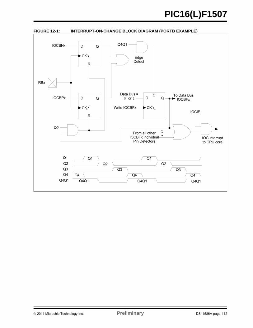
PIC16(L)F1507
FIGURE 12-1: INTERRUPT-ON-CHANGE BLOCK DIAGRAM (PORTB EXAMPLE)
D
CK
R
Q
D
CK
R
Q
RBx
IOCBNx
IOCBPx
Q2
D
CK
SQ
Q4Q1
Data Bus =0 or 1
Write IOCBFxIOCIE
To Data BusIOCBFx
EdgeDetect
IOC interruptto CPU core
From all other IOCBFx individual
Pin Detectors
Q1
Q2
Q3
Q4
Q4Q1
Q1
Q2
Q3
Q4
Q1
Q2
Q3
Q4Q4
Q4Q1 Q4Q1 Q4Q1
2011 Microchip Technology Inc. Preliminary DS41586A-page 112
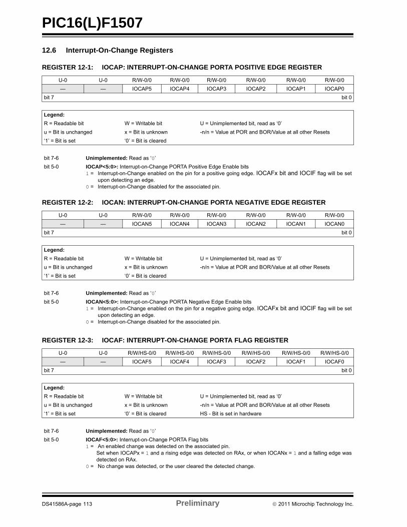
PIC16(L)F1507
12.6 Interrupt-On-Change Registers
REGISTER 12-1: IOCAP: INTERRUPT-ON-CHANGE PORTA POSITIVE EDGE REGISTER
U-0 U-0 R/W-0/0 R/W-0/0 R/W-0/0 R/W-0/0 R/W-0/0 R/W-0/0
— — IOCAP5 IOCAP4 IOCAP3 IOCAP2 IOCAP1 IOCAP0
bit 7 bit 0
Legend:
R = Readable bit W = Writable bit U = Unimplemented bit, read as ‘0’
u = Bit is unchanged x = Bit is unknown -n/n = Value at POR and BOR/Value at all other Resets
‘1’ = Bit is set ‘0’ = Bit is cleared
bit 7-6 Unimplemented: Read as ‘0’
bit 5-0 IOCAP<5:0>: Interrupt-on-Change PORTA Positive Edge Enable bits1 = Interrupt-on-Change enabled on the pin for a positive going edge. IOCAFx bit and IOCIF flag will be set
upon detecting an edge.0 = Interrupt-on-Change disabled for the associated pin.
REGISTER 12-2: IOCAN: INTERRUPT-ON-CHANGE PORTA NEGATIVE EDGE REGISTER
U-0 U-0 R/W-0/0 R/W-0/0 R/W-0/0 R/W-0/0 R/W-0/0 R/W-0/0
— — IOCAN5 IOCAN4 IOCAN3 IOCAN2 IOCAN1 IOCAN0
bit 7 bit 0
Legend:
R = Readable bit W = Writable bit U = Unimplemented bit, read as ‘0’
u = Bit is unchanged x = Bit is unknown -n/n = Value at POR and BOR/Value at all other Resets
‘1’ = Bit is set ‘0’ = Bit is cleared
bit 7-6 Unimplemented: Read as ‘0’
bit 5-0 IOCAN<5:0>: Interrupt-on-Change PORTA Negative Edge Enable bits1 = Interrupt-on-Change enabled on the pin for a negative going edge. IOCAFx bit and IOCIF flag will be set
upon detecting an edge.0 = Interrupt-on-Change disabled for the associated pin.
REGISTER 12-3: IOCAF: INTERRUPT-ON-CHANGE PORTA FLAG REGISTER
U-0 U-0 R/W/HS-0/0 R/W/HS-0/0 R/W/HS-0/0 R/W/HS-0/0 R/W/HS-0/0 R/W/HS-0/0
— — IOCAF5 IOCAF4 IOCAF3 IOCAF2 IOCAF1 IOCAF0
bit 7 bit 0
Legend:
R = Readable bit W = Writable bit U = Unimplemented bit, read as ‘0’
u = Bit is unchanged x = Bit is unknown -n/n = Value at POR and BOR/Value at all other Resets
‘1’ = Bit is set ‘0’ = Bit is cleared HS - Bit is set in hardware
bit 7-6 Unimplemented: Read as ‘0’
bit 5-0 IOCAF<5:0>: Interrupt-on-Change PORTA Flag bits1 = An enabled change was detected on the associated pin.
Set when IOCAPx = 1 and a rising edge was detected on RAx, or when IOCANx = 1 and a falling edge wasdetected on RAx.
0 = No change was detected, or the user cleared the detected change.
DS41586A-page 113 Preliminary 2011 Microchip Technology Inc.
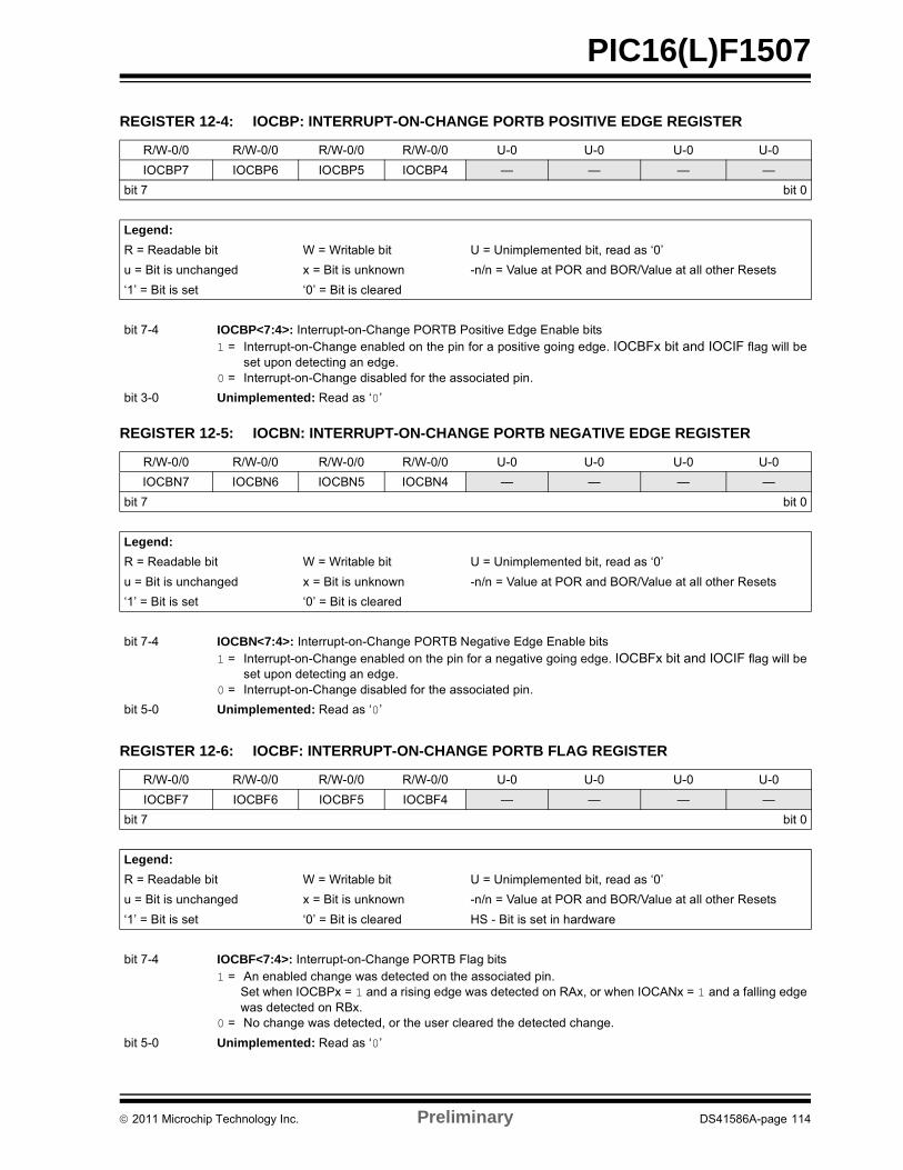
PIC16(L)F1507
REGISTER 12-4: IOCBP: INTERRUPT-ON-CHANGE PORTB POSITIVE EDGE REGISTER
R/W-0/0 R/W-0/0 R/W-0/0 R/W-0/0 U-0 U-0 U-0 U-0
IOCBP7 IOCBP6 IOCBP5 IOCBP4 — — — —
bit 7 bit 0
Legend:
R = Readable bit W = Writable bit U = Unimplemented bit, read as ‘0’
u = Bit is unchanged x = Bit is unknown -n/n = Value at POR and BOR/Value at all other Resets
‘1’ = Bit is set ‘0’ = Bit is cleared
bit 7-4 IOCBP<7:4>: Interrupt-on-Change PORTB Positive Edge Enable bits1 = Interrupt-on-Change enabled on the pin for a positive going edge. IOCBFx bit and IOCIF flag will be
set upon detecting an edge.0 = Interrupt-on-Change disabled for the associated pin.
bit 3-0 Unimplemented: Read as ‘0’
REGISTER 12-5: IOCBN: INTERRUPT-ON-CHANGE PORTB NEGATIVE EDGE REGISTER
R/W-0/0 R/W-0/0 R/W-0/0 R/W-0/0 U-0 U-0 U-0 U-0
IOCBN7 IOCBN6 IOCBN5 IOCBN4 — — — —
bit 7 bit 0
Legend:
R = Readable bit W = Writable bit U = Unimplemented bit, read as ‘0’
u = Bit is unchanged x = Bit is unknown -n/n = Value at POR and BOR/Value at all other Resets
‘1’ = Bit is set ‘0’ = Bit is cleared
bit 7-4 IOCBN<7:4>: Interrupt-on-Change PORTB Negative Edge Enable bits1 = Interrupt-on-Change enabled on the pin for a negative going edge. IOCBFx bit and IOCIF flag will be
set upon detecting an edge.0 = Interrupt-on-Change disabled for the associated pin.
bit 5-0 Unimplemented: Read as ‘0’
REGISTER 12-6: IOCBF: INTERRUPT-ON-CHANGE PORTB FLAG REGISTER
R/W-0/0 R/W-0/0 R/W-0/0 R/W-0/0 U-0 U-0 U-0 U-0
IOCBF7 IOCBF6 IOCBF5 IOCBF4 — — — —
bit 7 bit 0
Legend:
R = Readable bit W = Writable bit U = Unimplemented bit, read as ‘0’
u = Bit is unchanged x = Bit is unknown -n/n = Value at POR and BOR/Value at all other Resets
‘1’ = Bit is set ‘0’ = Bit is cleared HS - Bit is set in hardware
bit 7-4 IOCBF<7:4>: Interrupt-on-Change PORTB Flag bits1 = An enabled change was detected on the associated pin.
Set when IOCBPx = 1 and a rising edge was detected on RAx, or when IOCANx = 1 and a falling edgewas detected on RBx.
0 = No change was detected, or the user cleared the detected change.
bit 5-0 Unimplemented: Read as ‘0’
2011 Microchip Technology Inc. Preliminary DS41586A-page 114
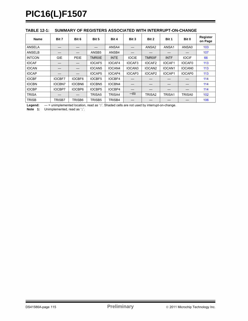
PIC16(L)F1507
TABLE 12-1: SUMMARY OF REGISTERS ASSOCIATED WITH INTERRUPT-ON-CHANGE
Name Bit 7 Bit 6 Bit 5 Bit 4 Bit 3 Bit 2 Bit 1 Bit 0Register on Page
ANSELA — — — ANSA4 — ANSA2 ANSA1 ANSA0 103
ANSELB — — ANSB5 ANSB4 — — — — 107
INTCON GIE PEIE TMR0IE INTE IOCIE TMR0IF INTF IOCIF 66
IOCAF — — IOCAF5 IOCAF4 IOCAF3 IOCAF2 IOCAF1 IOCAF0 113
IOCAN — — IOCAN5 IOCAN4 IOCAN3 IOCAN2 IOCAN1 IOCAN0 113
IOCAP — — IOCAP5 IOCAP4 IOCAP3 IOCAP2 IOCAP1 IOCAP0 113
IOCBF IOCBF7 IOCBF6 IOCBF5 IOCBF4 — — — — 114
IOCBN IOCBN7 IOCBN6 IOCBN5 IOCBN4 — — — — 114
IOCBP IOCBP7 IOCBP6 IOCBP5 IOCBP4 — — — — 114
TRISA — — TRISA5 TRISA4 —(1) TRISA2 TRISA1 TRISA0 102
TRISB TRISB7 TRISB6 TRISB5 TRISB4 — — — — 106
Legend: — = unimplemented location, read as ‘0’. Shaded cells are not used by interrupt-on-change.Note 1: Unimplemented, read as ‘1’.
DS41586A-page 115 Preliminary 2011 Microchip Technology Inc.

PIC16(L)F1507
NOTES:
2011 Microchip Technology Inc. Preliminary DS41586A-page 116
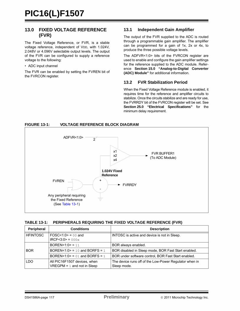
PIC16(L)F1507
13.0 FIXED VOLTAGE REFERENCE (FVR)
The Fixed Voltage Reference, or FVR, is a stablevoltage reference, independent of VDD, with 1.024V,2.048V or 4.096V selectable output levels. The outputof the FVR can be configured to supply a referencevoltage to the following:
• ADC input channel
The FVR can be enabled by setting the FVREN bit ofthe FVRCON register.
13.1 Independent Gain Amplifier
The output of the FVR supplied to the ADC is routedthrough a programmable gain amplifier. The amplifiercan be programmed for a gain of 1x, 2x or 4x, toproduce the three possible voltage levels.
The ADFVR<1:0> bits of the FVRCON register areused to enable and configure the gain amplifier settingsfor the reference supplied to the ADC module. Refer-ence Section 15.0 “Analog-to-Digital Converter(ADC) Module” for additional information.
13.2 FVR Stabilization Period
When the Fixed Voltage Reference module is enabled, itrequires time for the reference and amplifier circuits tostabilize. Once the circuits stabilize and are ready for use,the FVRRDY bit of the FVRCON register will be set. SeeSection 25.0 “Electrical Specifications” for theminimum delay requirement.
FIGURE 13-1: VOLTAGE REFERENCE BLOCK DIAGRAM
FVR BUFFER1(To ADC Module)
x1 x2 x4
+
-
1.024V FixedReference
FVRENFVRRDY
2ADFVR<1:0>
Any peripheral requiring the Fixed Reference
(See Table 13-1)
TABLE 13-1: PERIPHERALS REQUIRING THE FIXED VOLTAGE REFERENCE (FVR)
Peripheral Conditions Description
HFINTOSC FOSC<1:0> = 00 and IRCF<3:0> = 000x
INTOSC is active and device is not in Sleep.
BOR
BOREN<1:0> = 11 BOR always enabled.
BOREN<1:0> = 10 and BORFS = 1 BOR disabled in Sleep mode, BOR Fast Start enabled.
BOREN<1:0> = 01 and BORFS = 1 BOR under software control, BOR Fast Start enabled.
LDO All PIC16F1507 devices, when VREGPM = 1 and not in Sleep
The device runs off of the Low-Power Regulator when in Sleep mode.
DS41586A-page 117 Preliminary 2011 Microchip Technology Inc.
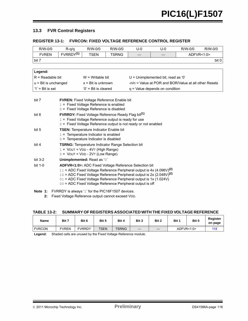
PIC16(L)F1507
13.3 FVR Control Registers
TABLE 13-2: SUMMARY OF REGISTERS ASSOCIATED WITH THE FIXED VOLTAGE REFERENCE
REGISTER 13-1: FVRCON: FIXED VOLTAGE REFERENCE CONTROL REGISTER
R/W-0/0 R-q/q R/W-0/0 R/W-0/0 U-0 U-0 R/W-0/0 R/W-0/0
FVREN FVRRDY(1) TSEN TSRNG — — ADFVR<1:0>
bit 7 bit 0
Legend:
R = Readable bit W = Writable bit U = Unimplemented bit, read as ‘0’
u = Bit is unchanged x = Bit is unknown -n/n = Value at POR and BOR/Value at all other Resets
‘1’ = Bit is set ‘0’ = Bit is cleared q = Value depends on condition
bit 7 FVREN: Fixed Voltage Reference Enable bit1 = Fixed Voltage Reference is enabled0 = Fixed Voltage Reference is disabled
bit 6 FVRRDY: Fixed Voltage Reference Ready Flag bit(1)
1 = Fixed Voltage Reference output is ready for use0 = Fixed Voltage Reference output is not ready or not enabled
bit 5 TSEN: Temperature Indicator Enable bit1 = Temperature Indicator is enabled0 = Temperature Indicator is disabled
bit 4 TSRNG: Temperature Indicator Range Selection bit1 = VOUT = VDD - 4VT (High Range)0 = VOUT = VDD - 2VT (Low Range)
bit 3-2 Unimplemented: Read as ‘0’
bit 1-0 ADFVR<1:0>: ADC Fixed Voltage Reference Selection bit11 = ADC Fixed Voltage Reference Peripheral output is 4x (4.096V)(2)
10 = ADC Fixed Voltage Reference Peripheral output is 2x (2.048V)(2)
01 = ADC Fixed Voltage Reference Peripheral output is 1x (1.024V)00 = ADC Fixed Voltage Reference Peripheral output is off
Note 1: FVRRDY is always ‘1’ for the PIC16F1507 devices.2: Fixed Voltage Reference output cannot exceed VDD.
Name Bit 7 Bit 6 Bit 5 Bit 4 Bit 3 Bit 2 Bit 1 Bit 0Register on page
FVRCON FVREN FVRRDY TSEN TSRNG — — ADFVR<1:0> 118
Legend: Shaded cells are unused by the Fixed Voltage Reference module.
2011 Microchip Technology Inc. Preliminary DS41586A-page 118
PIC16(L)F1507
14.0 TEMPERATURE INDICATOR MODULE
This family of devices is equipped with a temperaturecircuit designed to measure the operating temperatureof the silicon die. The circuit’s range of operatingtemperature falls between -40°C and +85°C. Theoutput is a voltage that is proportional to the devicetemperature. The output of the temperature indicator isinternally connected to the device ADC.
The circuit may be used as a temperature thresholddetector or a more accurate temperature indicator,depending on the level of calibration performed. A one-point calibration allows the circuit to indicate atemperature closely surrounding that point. A two-pointcalibration allows the circuit to sense the entire rangeof temperature more accurately. Reference ApplicationNote AN1333, “Use and Calibration of the InternalTemperature Indicator” (DS01333) for more detailsregarding the calibration process.
14.1 Circuit Operation
Figure 14-1 shows a simplified block diagram of thetemperature circuit. The proportional voltage output isachieved by measuring the forward voltage drop acrossmultiple silicon junctions.
Equation 14-1 describes the output characteristics ofthe temperature indicator.
EQUATION 14-1: VOUT RANGES
The temperature sense circuit is integrated with theFixed Voltage Reference (FVR) module. SeeSection 13.0 “Fixed Voltage Reference (FVR)” formore information.
The circuit is enabled by setting the TSEN bit of theFVRCON register. When disabled, the circuit draws nocurrent.
The circuit operates in either high or low range. The highrange, selected by setting the TSRNG bit of theFVRCON register, provides a wider output voltage. Thisprovides more resolution over the temperature range,but may be less consistent from part to part. This rangerequires a higher bias voltage to operate and thus, ahigher VDD is needed.
The low range is selected by clearing the TSRNG bit ofthe FVRCON register. The low range generates a lowervoltage drop and thus, a lower bias voltage is needed tooperate the circuit. The low range is provided for lowvoltage operation.
FIGURE 14-1: TEMPERATURE CIRCUIT DIAGRAM
14.2 Minimum Operating VDD
When the temperature circuit is operated in low range,the device may be operated at any operating voltagethat is within specifications.
When the temperature circuit is operated in high range,the device operating voltage, VDD, must be highenough to ensure that the temperature circuit is cor-rectly biased.
Table 14-1 shows the recommended minimum VDD vs.range setting.
TABLE 14-1: RECOMMENDED VDD VS. RANGE
14.3 Temperature Output
The output of the circuit is measured using the internalAnalog-to-Digital Converter. A channel is reserved forthe temperature circuit output. Refer to Section 15.0“Analog-to-Digital Converter (ADC) Module” fordetailed information.
14.4 ADC Acquisition Time
To ensure accurate temperature measurements, theuser must wait at least 200 s after the ADC inputmultiplexer is connected to the temperature indicatoroutput before the conversion is performed. In addition,the user must wait 200 s between sequentialconversions of the temperature indicator output.
High Range: VOUT = VDD - 4VT
Low Range: VOUT = VDD - 2VT
Min. VDD, TSRNG = 1 Min. VDD, TSRNG = 0
3.6V 1.8V
TSEN
TSRNG
VDD
VOUTTo ADC
DS41586A-page 119 Preliminary 2011 Microchip Technology Inc.
PIC16(L)F1507
TABLE 14-2: SUMMARY OF REGISTERS ASSOCIATED WITH THE TEMPERATURE INDICATOR
Name Bit 7 Bit 6 Bit 5 Bit 4 Bit 3 Bit 2 Bit 1 Bit 0Register on page
FVRCON FVREN FVRRDY TSEN TSRNG — — ADFVR<1:0> 118
Legend: Shaded cells are unused by the temperature indicator module.
2011 Microchip Technology Inc. Preliminary DS41586A-page 120
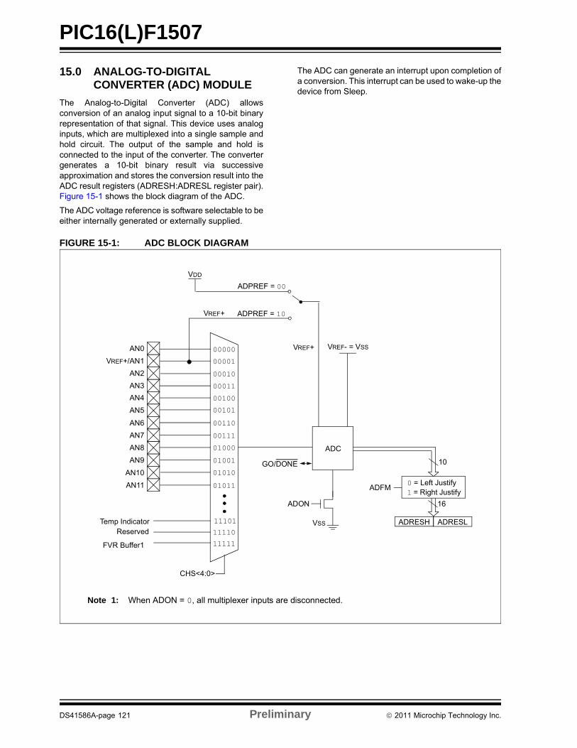
PIC16(L)F1507
15.0 ANALOG-TO-DIGITAL CONVERTER (ADC) MODULE
The Analog-to-Digital Converter (ADC) allowsconversion of an analog input signal to a 10-bit binaryrepresentation of that signal. This device uses analoginputs, which are multiplexed into a single sample andhold circuit. The output of the sample and hold isconnected to the input of the converter. The convertergenerates a 10-bit binary result via successiveapproximation and stores the conversion result into theADC result registers (ADRESH:ADRESL register pair).Figure 15-1 shows the block diagram of the ADC.
The ADC voltage reference is software selectable to beeither internally generated or externally supplied.
The ADC can generate an interrupt upon completion ofa conversion. This interrupt can be used to wake-up thedevice from Sleep.
FIGURE 15-1: ADC BLOCK DIAGRAM
VDD
VREF+ ADPREF = 10
ADPREF = 00
FVR Buffer1
Note 1: When ADON = 0, all multiplexer inputs are disconnected.
ADON
GO/DONE
VSS
ADC
00000
00001
00010
00011
00100
00101
00111
00110
01000
01001
01010
01011
CHS<4:0>
AN0
VREF+/AN1
AN2
AN4
AN5
AN6
AN7
AN3
AN8
AN9
AN10
AN11
11111
ADRESH ADRESL
10
16
ADFM0 = Left Justify1 = Right Justify
Reserved 11110
VREF- = VSSVREF+
11101 Temp Indicator
DS41586A-page 121 Preliminary 2011 Microchip Technology Inc.
PIC16(L)F1507
15.1 ADC Configuration
When configuring and using the ADC the followingfunctions must be considered:
• Port configuration
• Channel selection
• ADC voltage reference selection
• ADC conversion clock source
• Interrupt control
• Result formatting
15.1.1 PORT CONFIGURATION
The ADC can be used to convert both analog anddigital signals. When converting analog signals, the I/Opin should be configured for analog by setting theassociated TRIS and ANSEL bits. Refer toSection 11.0 “I/O Ports” for more information.
15.1.2 CHANNEL SELECTION
There are 14 channel selections available:
• AN<11:0> pins
• Temperature Indicator
• FVR (Fixed Voltage Reference) Output
Refer to Section 13.0 “Fixed Voltage Reference (FVR)”and Section 14.0 “Temperature Indicator Module” formore information on these channel selections.
The CHS bits of the ADCON0 register determine whichchannel is connected to the sample and hold circuit.
When changing channels, a delay is required beforestarting the next conversion. Refer to Section 15.2“ADC Operation” for more information.
15.1.3 ADC VOLTAGE REFERENCE
The ADPREF bits of the ADCON1 register providescontrol of the positive voltage reference. The positivevoltage reference can be:
• VREF+ pin
• VDD
• FVR 2.048V
• FVR 4.096V (Not available on LF devices)
See Section 13.0 “Fixed Voltage Reference (FVR)”for more details on the Fixed Voltage Reference.
15.1.4 CONVERSION CLOCK
The source of the conversion clock is software select-able via the ADCS bits of the ADCON1 register. Thereare seven possible clock options:
• FOSC/2
• FOSC/4
• FOSC/8
• FOSC/16
• FOSC/32
• FOSC/64
• FRC (dedicated internal oscillator)
The time to complete one bit conversion is defined asTAD. One full 10-bit conversion requires 11.5 TAD peri-ods as shown in Figure 15-2.
For correct conversion, the appropriate TAD specifica-tion must be met. Refer to the A/D conversion require-ments in Section 25.0 “Electrical Specifications” formore information. Table 15-1 gives examples of appro-priate ADC clock selections.
Note: Analog voltages on any pin that is definedas a digital input may cause the input buf-fer to conduct excess current.
Note: Unless using the FRC, any changes in thesystem clock frequency will change theADC clock frequency, which mayadversely affect the ADC result.
2011 Microchip Technology Inc. Preliminary DS41586A-page 122
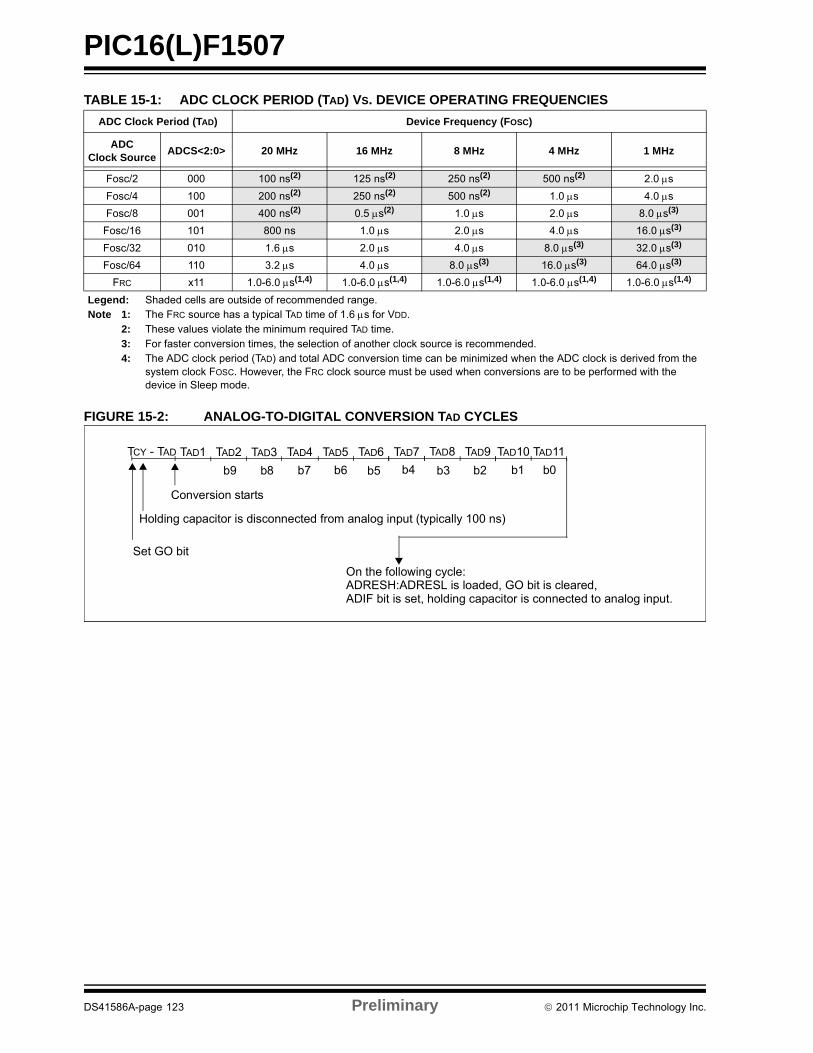
PIC16(L)F1507
TABLE 15-1: ADC CLOCK PERIOD (TAD) VS. DEVICE OPERATING FREQUENCIES
FIGURE 15-2: ANALOG-TO-DIGITAL CONVERSION TAD CYCLES
ADC Clock Period (TAD) Device Frequency (FOSC)
ADCClock Source
ADCS<2:0> 20 MHz 16 MHz 8 MHz 4 MHz 1 MHz
Fosc/2 000 100 ns(2) 125 ns(2) 250 ns(2) 500 ns(2) 2.0 s
Fosc/4 100 200 ns(2) 250 ns(2) 500 ns(2) 1.0 s 4.0 s
Fosc/8 001 400 ns(2) 0.5 s(2) 1.0 s 2.0 s 8.0 s(3)
Fosc/16 101 800 ns 1.0 s 2.0 s 4.0 s 16.0 s(3)
Fosc/32 010 1.6 s 2.0 s 4.0 s 8.0 s(3) 32.0 s(3)
Fosc/64 110 3.2 s 4.0 s 8.0 s(3) 16.0 s(3) 64.0 s(3)
FRC x11 1.0-6.0 s(1,4) 1.0-6.0 s(1,4) 1.0-6.0 s(1,4) 1.0-6.0 s(1,4) 1.0-6.0 s(1,4)
Legend: Shaded cells are outside of recommended range.Note 1: The FRC source has a typical TAD time of 1.6 s for VDD.
2: These values violate the minimum required TAD time.3: For faster conversion times, the selection of another clock source is recommended.4: The ADC clock period (TAD) and total ADC conversion time can be minimized when the ADC clock is derived from the
system clock FOSC. However, the FRC clock source must be used when conversions are to be performed with the device in Sleep mode.
TAD1 TAD2 TAD3 TAD4 TAD5 TAD6 TAD7 TAD8 TAD11
Set GO bit
Holding capacitor is disconnected from analog input (typically 100 ns)
TAD9 TAD10TCY - TAD
ADRESH:ADRESL is loaded, GO bit is cleared, ADIF bit is set, holding capacitor is connected to analog input.
Conversion starts
b0b9 b6 b5 b4 b3 b2 b1b8 b7
On the following cycle:
DS41586A-page 123 Preliminary 2011 Microchip Technology Inc.
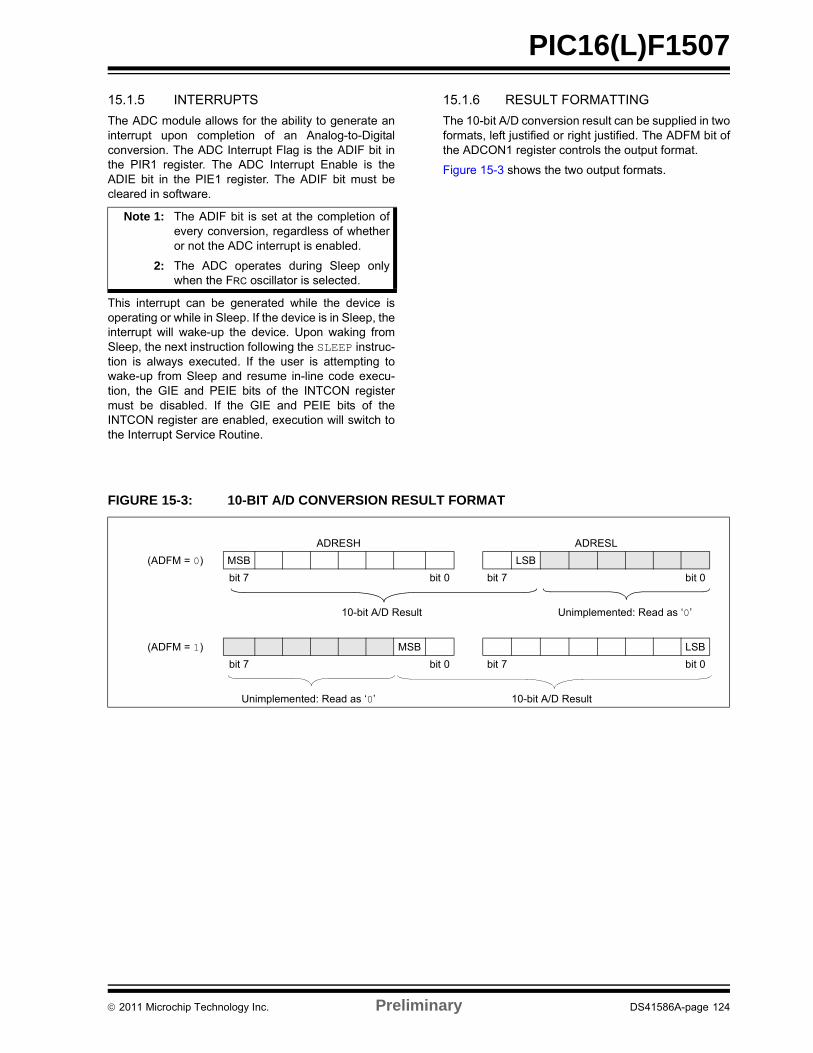
PIC16(L)F1507
15.1.5 INTERRUPTS
The ADC module allows for the ability to generate aninterrupt upon completion of an Analog-to-Digitalconversion. The ADC Interrupt Flag is the ADIF bit inthe PIR1 register. The ADC Interrupt Enable is theADIE bit in the PIE1 register. The ADIF bit must becleared in software.
This interrupt can be generated while the device isoperating or while in Sleep. If the device is in Sleep, theinterrupt will wake-up the device. Upon waking fromSleep, the next instruction following the SLEEP instruc-tion is always executed. If the user is attempting towake-up from Sleep and resume in-line code execu-tion, the GIE and PEIE bits of the INTCON registermust be disabled. If the GIE and PEIE bits of theINTCON register are enabled, execution will switch tothe Interrupt Service Routine.
15.1.6 RESULT FORMATTING
The 10-bit A/D conversion result can be supplied in twoformats, left justified or right justified. The ADFM bit ofthe ADCON1 register controls the output format.
Figure 15-3 shows the two output formats.
FIGURE 15-3: 10-BIT A/D CONVERSION RESULT FORMAT
Note 1: The ADIF bit is set at the completion ofevery conversion, regardless of whetheror not the ADC interrupt is enabled.
2: The ADC operates during Sleep onlywhen the FRC oscillator is selected.
ADRESH ADRESL
(ADFM = 0) MSB LSB
bit 7 bit 0 bit 7 bit 0
10-bit A/D Result Unimplemented: Read as ‘0’
(ADFM = 1) MSB LSB
bit 7 bit 0 bit 7 bit 0
Unimplemented: Read as ‘0’ 10-bit A/D Result
2011 Microchip Technology Inc. Preliminary DS41586A-page 124
PIC16(L)F1507
15.2 ADC Operation
15.2.1 STARTING A CONVERSION
To enable the ADC module, the ADON bit of theADCON0 register must be set to a ‘1’. Setting the GO/DONE bit of the ADCON0 register to a ‘1’ will start theAnalog-to-Digital conversion.
15.2.2 COMPLETION OF A CONVERSION
When the conversion is complete, the ADC module will:
• Clear the GO/DONE bit
• Set the ADIF Interrupt Flag bit
• Update the ADRESH and ADRESL registers with new conversion result
15.2.3 TERMINATING A CONVERSION
If a conversion must be terminated before completion,the GO/DONE bit can be cleared in software. TheADRESH and ADRESL registers will be updated withthe partially complete Analog-to-Digital conversionsample. Incomplete bits will match the last bitconverted.
15.2.4 ADC OPERATION DURING SLEEP
The ADC module can operate during Sleep. Thisrequires the ADC clock source to be set to the FRC
option. When the FRC clock source is selected, theADC waits one additional instruction before starting theconversion. This allows the SLEEP instruction to beexecuted, which can reduce system noise during theconversion. If the ADC interrupt is enabled, the devicewill wake-up from Sleep when the conversioncompletes. If the ADC interrupt is disabled, the ADCmodule is turned off after the conversion completes,although the ADON bit remains set.
When the ADC clock source is something other thanFRC, a SLEEP instruction causes the present conver-sion to be aborted and the ADC module is turned off,although the ADON bit remains set.
15.2.5 AUTO-CONVERSION TRIGGER
The auto-conversion trigger allows periodic ADC mea-surements without software intervention. When a risingedge of the selected source occurs, the GO/DONE bitis set by hardware.
The auto-conversion trigger source is selected with theTRIGSEL<3:0> bits of the ADCON2 register.
Using the auto-conversion trigger does not assureproper ADC timing. It is the user’s responsibility toensure that the ADC timing requirements are met.
Auto-Conversion sources are:
• TMR0
• TMR1
• TMR2
• CLC1
• CLC2
Note: The GO/DONE bit should not be set in thesame instruction that turns on the ADC.Refer to Section 15.2.6 “A/D Conver-sion Procedure”.
Note: A device Reset forces all registers to theirReset state. Thus, the ADC module isturned off and any pending conversion isterminated.
DS41586A-page 125 Preliminary 2011 Microchip Technology Inc.
PIC16(L)F1507
15.2.6 A/D CONVERSION PROCEDURE
This is an example procedure for using the ADC toperform an Analog-to-Digital conversion:
1. Configure Port:
• Disable pin output driver (Refer to the TRIS register)
• Configure pin as analog (Refer to the ANSEL register)
2. Configure the ADC module:
• Select ADC conversion clock
• Configure voltage reference
• Select ADC input channel
• Turn on ADC module
3. Configure ADC interrupt (optional):
• Clear ADC interrupt flag
• Enable ADC interrupt
• Enable peripheral interrupt
• Enable global interrupt(1)
4. Wait the required acquisition time(2).
5. Start conversion by setting the GO/DONE bit.
6. Wait for ADC conversion to complete by one ofthe following:
• Polling the GO/DONE bit
• Waiting for the ADC interrupt (interrupts enabled)
7. Read ADC Result.
8. Clear the ADC interrupt flag (required if interruptis enabled).
EXAMPLE 15-1: A/D CONVERSION
Note 1: The global interrupt can be disabled if theuser is attempting to wake-up from Sleepand resume in-line code execution.
2: Refer to Section 15.3 “A/D AcquisitionRequirements”.
;This code block configures the ADC;for polling, Vdd and Vss references, Frc ;clock and AN0 input.;;Conversion start & polling for completion ; are included.;BANKSEL ADCON1 ;MOVLW B’11110000’ ;Right justify, Frc
;clockMOVWF ADCON1 ;Vdd and Vss Vref+BANKSEL TRISA ;BSF TRISA,0 ;Set RA0 to inputBANKSEL ANSEL ;BSF ANSEL,0 ;Set RA0 to analogBANKSEL ADCON0 ;MOVLW B’00000001’ ;Select channel AN0MOVWF ADCON0 ;Turn ADC OnCALL SampleTime ;Acquisiton delayBSF ADCON0,ADGO ;Start conversionBTFSC ADCON0,ADGO ;Is conversion done?GOTO $-1 ;No, test againBANKSEL ADRESH ;MOVF ADRESH,W ;Read upper 2 bitsMOVWF RESULTHI ;store in GPR spaceBANKSEL ADRESL ;MOVF ADRESL,W ;Read lower 8 bitsMOVWF RESULTLO ;Store in GPR space
2011 Microchip Technology Inc. Preliminary DS41586A-page 126
PIC16(L)F1507
15.2.7 ADC REGISTER DEFINITIONS
The following registers are used to control theoperation of the ADC.
REGISTER 15-1: ADCON0: A/D CONTROL REGISTER 0
U-0 R/W-0/0 R/W-0/0 R/W-0/0 R/W-0/0 R/W-0/0 R/W-0/0 R/W-0/0
— CHS<4:0> GO/DONE ADON
bit 7 bit 0
Legend:
R = Readable bit W = Writable bit U = Unimplemented bit, read as ‘0’
u = Bit is unchanged x = Bit is unknown -n/n = Value at POR and BOR/Value at all other Resets
‘1’ = Bit is set ‘0’ = Bit is cleared
bit 7 Unimplemented: Read as ‘0’
bit 6-2 CHS<4:0>: Analog Channel Select bits
00000 = AN000001 = AN100010 = AN200011 = AN300100 = AN400101 = AN500110 = AN600111 = AN701000 = AN801001 = AN901010 = AN1001011 = AN1101100 = Reserved. No channel connected.
• • •
11101 = Temperature Indicator(2)
11110 = Reserved. No channel connected11111 = FVR (Fixed Voltage Reference) Buffer 1 Output(1)
bit 1 GO/DONE: A/D Conversion Status bit
1 = A/D conversion cycle in progress. Setting this bit starts an A/D conversion cycle. This bit is automatically cleared by hardware when the A/D conversion has completed.0 = A/D conversion completed/not in progress
bit 0 ADON: ADC Enable bit1 = ADC is enabled0 = ADC is disabled and consumes no operating current
Note 1: See Section 13.0 “Fixed Voltage Reference (FVR)” for more information.
2: See Section 14.0 “Temperature Indicator Module” for more information.
DS41586A-page 127 Preliminary 2011 Microchip Technology Inc.
PIC16(L)F1507
REGISTER 15-2: ADCON1: A/D CONTROL REGISTER 1
R/W-0/0 R/W-0/0 R/W-0/0 R/W-0/0 U-0 U-0 R/W-0/0 R/W-0/0
ADFM ADCS<2:0> — — ADPREF<1:0>
bit 7 bit 0
Legend:
R = Readable bit W = Writable bit U = Unimplemented bit, read as ‘0’
u = Bit is unchanged x = Bit is unknown -n/n = Value at POR and BOR/Value at all other Resets
‘1’ = Bit is set ‘0’ = Bit is cleared
bit 7 ADFM: A/D Result Format Select bit1 = Right justified. Six Most Significant bits of ADRESH are set to ‘0’ when the conversion result is
loaded.0 = Left justified. Six Least Significant bits of ADRESL are set to ‘0’ when the conversion result is
loaded.
bit 6-4 ADCS<2:0>: A/D Conversion Clock Select bits000 = FOSC/2001 = FOSC/8010 = FOSC/32011 = FRC (clock supplied from a dedicated RC oscillator)100 = FOSC/4101 = FOSC/16110 = FOSC/64111 = FRC (clock supplied from a dedicated RC oscillator)
bit 3-2 Unimplemented: Read as ‘0’
bit 1-0 ADPREF<1:0>: A/D Positive Voltage Reference Configuration bits00 = VREF+ is connected to VDD
01 = Reserved10 = VREF+ is connected to external VREF+ pin(1)
11 = Reserved
Note 1: When selecting the VREF+ pin as the source of the positive reference, be aware that a minimum voltage specification exists. See Section 25.0 “Electrical Specifications” for details.
2011 Microchip Technology Inc. Preliminary DS41586A-page 128
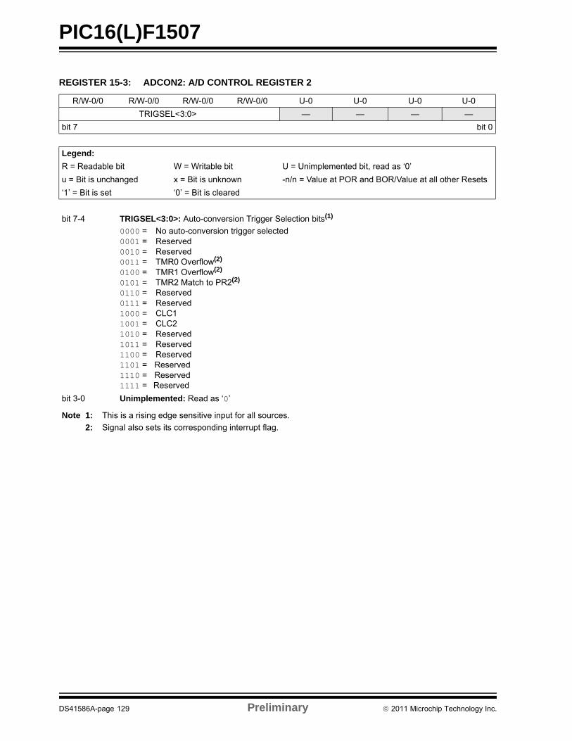
PIC16(L)F1507
REGISTER 15-3: ADCON2: A/D CONTROL REGISTER 2
R/W-0/0 R/W-0/0 R/W-0/0 R/W-0/0 U-0 U-0 U-0 U-0
TRIGSEL<3:0> — — — —
bit 7 bit 0
Legend:
R = Readable bit W = Writable bit U = Unimplemented bit, read as ‘0’
u = Bit is unchanged x = Bit is unknown -n/n = Value at POR and BOR/Value at all other Resets
‘1’ = Bit is set ‘0’ = Bit is cleared
bit 7-4 TRIGSEL<3:0>: Auto-conversion Trigger Selection bits(1)
0000 = No auto-conversion trigger selected0001 = Reserved0010 = Reserved0011 = TMR0 Overflow(2)
0100 = TMR1 Overflow(2)
0101 = TMR2 Match to PR2(2)
0110 = Reserved0111 = Reserved1000 = CLC11001 = CLC21010 = Reserved1011 = Reserved1100 = Reserved1101 = Reserved1110 = Reserved1111 = Reserved
bit 3-0 Unimplemented: Read as ‘0’
Note 1: This is a rising edge sensitive input for all sources.
2: Signal also sets its corresponding interrupt flag.
DS41586A-page 129 Preliminary 2011 Microchip Technology Inc.
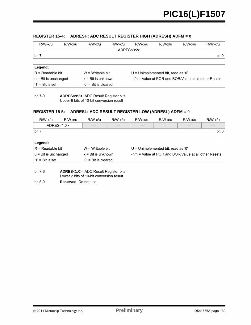
PIC16(L)F1507
REGISTER 15-4: ADRESH: ADC RESULT REGISTER HIGH (ADRESH) ADFM = 0
R/W-x/u R/W-x/u R/W-x/u R/W-x/u R/W-x/u R/W-x/u R/W-x/u R/W-x/u
ADRES<9:2>
bit 7 bit 0
Legend:
R = Readable bit W = Writable bit U = Unimplemented bit, read as ‘0’
u = Bit is unchanged x = Bit is unknown -n/n = Value at POR and BOR/Value at all other Resets
‘1’ = Bit is set ‘0’ = Bit is cleared
bit 7-0 ADRES<9:2>: ADC Result Register bitsUpper 8 bits of 10-bit conversion result
REGISTER 15-5: ADRESL: ADC RESULT REGISTER LOW (ADRESL) ADFM = 0
R/W-x/u R/W-x/u R/W-x/u R/W-x/u R/W-x/u R/W-x/u R/W-x/u R/W-x/u
ADRES<1:0> — — — — — —
bit 7 bit 0
Legend:
R = Readable bit W = Writable bit U = Unimplemented bit, read as ‘0’
u = Bit is unchanged x = Bit is unknown -n/n = Value at POR and BOR/Value at all other Resets
‘1’ = Bit is set ‘0’ = Bit is cleared
bit 7-6 ADRES<1:0>: ADC Result Register bitsLower 2 bits of 10-bit conversion result
bit 5-0 Reserved: Do not use.
2011 Microchip Technology Inc. Preliminary DS41586A-page 130
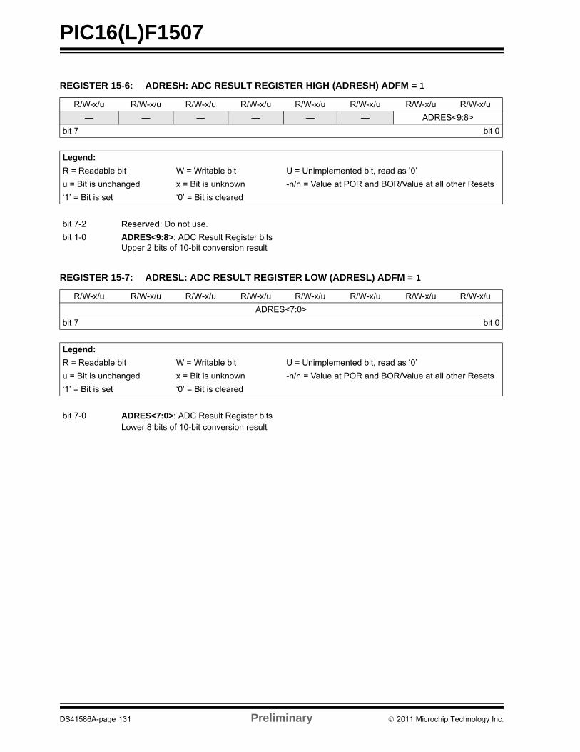
PIC16(L)F1507
REGISTER 15-6: ADRESH: ADC RESULT REGISTER HIGH (ADRESH) ADFM = 1
R/W-x/u R/W-x/u R/W-x/u R/W-x/u R/W-x/u R/W-x/u R/W-x/u R/W-x/u
— — — — — — ADRES<9:8>
bit 7 bit 0
Legend:
R = Readable bit W = Writable bit U = Unimplemented bit, read as ‘0’
u = Bit is unchanged x = Bit is unknown -n/n = Value at POR and BOR/Value at all other Resets
‘1’ = Bit is set ‘0’ = Bit is cleared
bit 7-2 Reserved: Do not use.
bit 1-0 ADRES<9:8>: ADC Result Register bitsUpper 2 bits of 10-bit conversion result
REGISTER 15-7: ADRESL: ADC RESULT REGISTER LOW (ADRESL) ADFM = 1
R/W-x/u R/W-x/u R/W-x/u R/W-x/u R/W-x/u R/W-x/u R/W-x/u R/W-x/u
ADRES<7:0>
bit 7 bit 0
Legend:
R = Readable bit W = Writable bit U = Unimplemented bit, read as ‘0’
u = Bit is unchanged x = Bit is unknown -n/n = Value at POR and BOR/Value at all other Resets
‘1’ = Bit is set ‘0’ = Bit is cleared
bit 7-0 ADRES<7:0>: ADC Result Register bitsLower 8 bits of 10-bit conversion result
DS41586A-page 131 Preliminary 2011 Microchip Technology Inc.
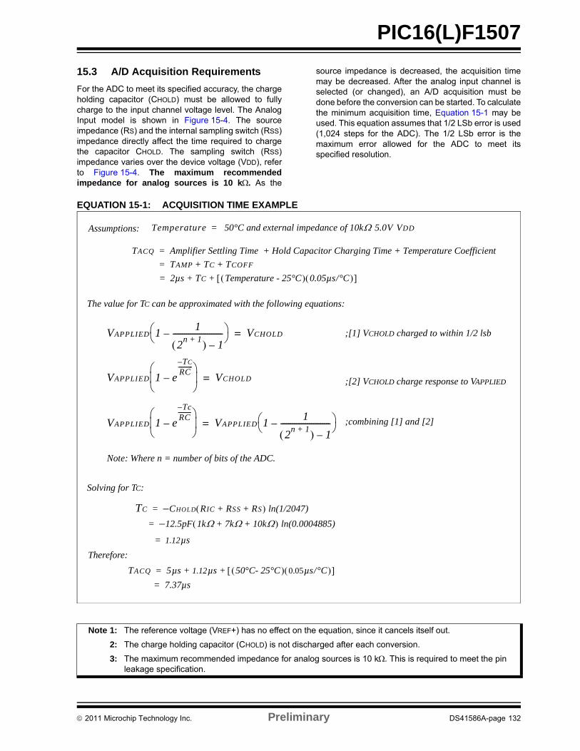
PIC16(L)F1507
15.3 A/D Acquisition Requirements
For the ADC to meet its specified accuracy, the chargeholding capacitor (CHOLD) must be allowed to fullycharge to the input channel voltage level. The AnalogInput model is shown in Figure 15-4. The sourceimpedance (RS) and the internal sampling switch (RSS)impedance directly affect the time required to chargethe capacitor CHOLD. The sampling switch (RSS)impedance varies over the device voltage (VDD), referto Figure 15-4. The maximum recommendedimpedance for analog sources is 10 k. As the
source impedance is decreased, the acquisition timemay be decreased. After the analog input channel isselected (or changed), an A/D acquisition must bedone before the conversion can be started. To calculatethe minimum acquisition time, Equation 15-1 may beused. This equation assumes that 1/2 LSb error is used(1,024 steps for the ADC). The 1/2 LSb error is themaximum error allowed for the ADC to meet itsspecified resolution.
EQUATION 15-1: ACQUISITION TIME EXAMPLE
TACQ Amplifier Settling Time Hold Capacitor Charging Time Temperature Coefficient+ +=
TAMP TC TCOFF+ +=
2µs TC Temperature - 25°C 0.05µs/°C + +=
TC CHOLD RIC RSS RS+ + ln(1/2047)–=
12.5pF 1k 7k 10k+ + – ln(0.0004885)=
1.12= µs
VAPPLIED 1 e
Tc–RC---------
–
VAPPLIED 11
2n 1+ 1–
--------------------------– =
VAPPLIED 11
2n 1+ 1–
--------------------------– VCHOLD=
VAPPLIED 1 e
TC–RC----------
–
VCHOLD=
;[1] VCHOLD charged to within 1/2 lsb
;[2] VCHOLD charge response to VAPPLIED
;combining [1] and [2]
The value for TC can be approximated with the following equations:
Solving for TC:
Therefore:
Temperature 50°C and external impedance of 10k 5.0V VDD=Assumptions:
Note: Where n = number of bits of the ADC.
TACQ 5µs 1.12µs 50°C- 25°C 0.05µs/°C + +=
7.37µs=
Note 1: The reference voltage (VREF+) has no effect on the equation, since it cancels itself out.
2: The charge holding capacitor (CHOLD) is not discharged after each conversion.
3: The maximum recommended impedance for analog sources is 10 k. This is required to meet the pin leakage specification.
2011 Microchip Technology Inc. Preliminary DS41586A-page 132
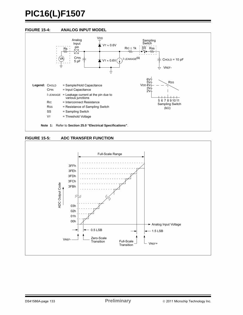
PIC16(L)F1507
FIGURE 15-4: ANALOG INPUT MODEL
FIGURE 15-5: ADC TRANSFER FUNCTION
CPINVA
Rs
Analog
5 pF
VDD
VT 0.6V
VT 0.6V I LEAKAGE(1)
RIC 1k
SamplingSwitch
SS Rss
CHOLD = 10 pF
VREF-
6V
Sampling Switch
5V4V3V2V
5 6 7 8 9 10 11
(k)
VDD
Legend:
CPIN
VT
I LEAKAGE
RIC
SS
CHOLD
= Input Capacitance
= Threshold Voltage
= Leakage current at the pin due to
= Interconnect Resistance
= Sampling Switch
= Sample/Hold Capacitance
various junctions
RSS
Note 1: Refer to Section 25.0 “Electrical Specifications”.
RSS = Resistance of Sampling Switch
Inputpin
3FFh
3FEh
AD
C O
utp
ut C
od
e
3FDh
3FCh
03h
02h
01h
00h
Full-Scale
3FBh
0.5 LSB
VREF- Zero-ScaleTransition
VREF+Transition
1.5 LSB
Full-Scale Range
Analog Input Voltage
DS41586A-page 133 Preliminary 2011 Microchip Technology Inc.
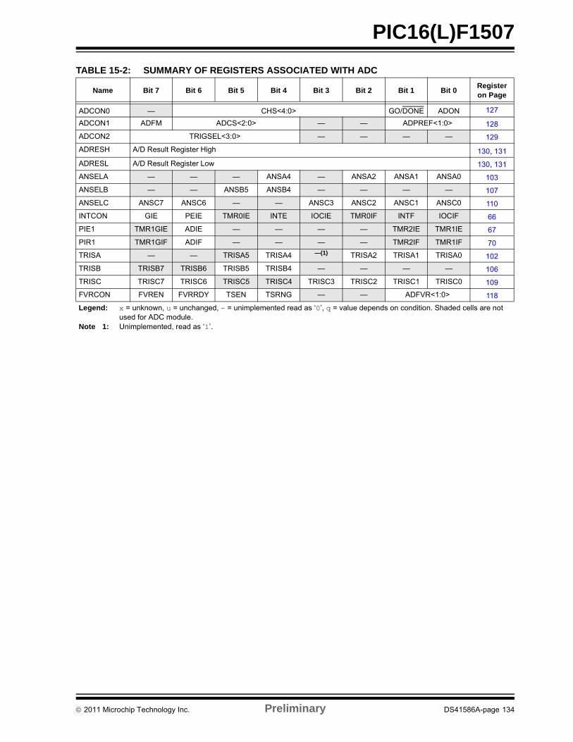
PIC16(L)F1507
TABLE 15-2: SUMMARY OF REGISTERS ASSOCIATED WITH ADC
Name Bit 7 Bit 6 Bit 5 Bit 4 Bit 3 Bit 2 Bit 1 Bit 0Register on Page
ADCON0 — CHS<4:0> GO/DONE ADON 127
ADCON1 ADFM ADCS<2:0> — — ADPREF<1:0> 128
ADCON2 TRIGSEL<3:0> — — — — 129
ADRESH A/D Result Register High 130, 131
ADRESL A/D Result Register Low 130, 131
ANSELA — — — ANSA4 — ANSA2 ANSA1 ANSA0 103
ANSELB — — ANSB5 ANSB4 — — — — 107
ANSELC ANSC7 ANSC6 — — ANSC3 ANSC2 ANSC1 ANSC0 110
INTCON GIE PEIE TMR0IE INTE IOCIE TMR0IF INTF IOCIF 66
PIE1 TMR1GIE ADIE — — — — TMR2IE TMR1IE 67
PIR1 TMR1GIF ADIF — — — — TMR2IF TMR1IF 70
TRISA — — TRISA5 TRISA4 —(1) TRISA2 TRISA1 TRISA0 102
TRISB TRISB7 TRISB6 TRISB5 TRISB4 — — — — 106
TRISC TRISC7 TRISC6 TRISC5 TRISC4 TRISC3 TRISC2 TRISC1 TRISC0 109
FVRCON FVREN FVRRDY TSEN TSRNG — — ADFVR<1:0> 118
Legend: x = unknown, u = unchanged, — = unimplemented read as ‘0’, q = value depends on condition. Shaded cells are not used for ADC module.
Note 1: Unimplemented, read as ‘1’.
2011 Microchip Technology Inc. Preliminary DS41586A-page 134
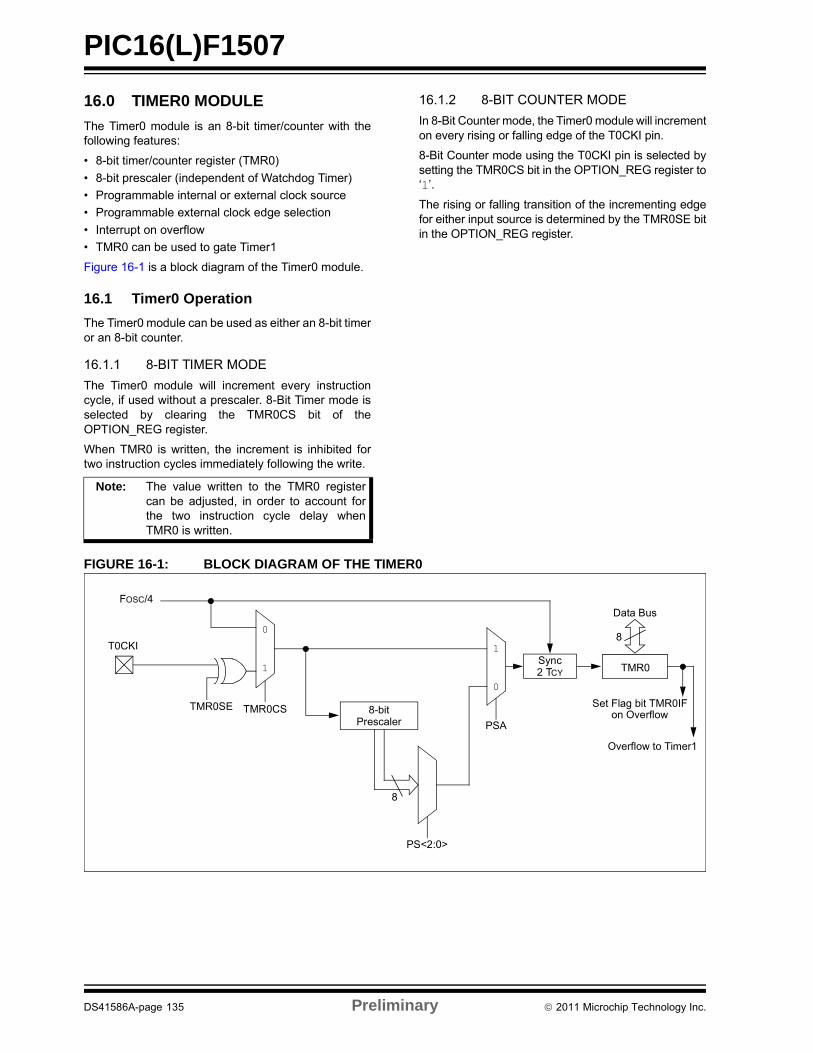
PIC16(L)F1507
16.0 TIMER0 MODULE
The Timer0 module is an 8-bit timer/counter with thefollowing features:
• 8-bit timer/counter register (TMR0)
• 8-bit prescaler (independent of Watchdog Timer)
• Programmable internal or external clock source
• Programmable external clock edge selection
• Interrupt on overflow
• TMR0 can be used to gate Timer1
Figure 16-1 is a block diagram of the Timer0 module.
16.1 Timer0 Operation
The Timer0 module can be used as either an 8-bit timeror an 8-bit counter.
16.1.1 8-BIT TIMER MODE
The Timer0 module will increment every instructioncycle, if used without a prescaler. 8-Bit Timer mode isselected by clearing the TMR0CS bit of theOPTION_REG register.
When TMR0 is written, the increment is inhibited fortwo instruction cycles immediately following the write.
16.1.2 8-BIT COUNTER MODE
In 8-Bit Counter mode, the Timer0 module will incrementon every rising or falling edge of the T0CKI pin.
8-Bit Counter mode using the T0CKI pin is selected bysetting the TMR0CS bit in the OPTION_REG register to‘1’.
The rising or falling transition of the incrementing edgefor either input source is determined by the TMR0SE bitin the OPTION_REG register.
FIGURE 16-1: BLOCK DIAGRAM OF THE TIMER0
Note: The value written to the TMR0 registercan be adjusted, in order to account forthe two instruction cycle delay whenTMR0 is written.
T0CKI
TMR0SE
TMR0
PS<2:0>
Data Bus
Set Flag bit TMR0IFon OverflowTMR0CS
0
1
0
18
8
8-bitPrescaler
FOSC/4
PSA
Sync2 TCY
Overflow to Timer1
DS41586A-page 135 Preliminary 2011 Microchip Technology Inc.
PIC16(L)F1507
16.1.3 SOFTWARE PROGRAMMABLE PRESCALER
A software programmable prescaler is available forexclusive use with Timer0. The prescaler is enabled byclearing the PSA bit of the OPTION_REG register.
There are 8 prescaler options for the Timer0 moduleranging from 1:2 to 1:256. The prescale values areselectable via the PS<2:0> bits of the OPTION_REGregister. In order to have a 1:1 prescaler value for theTimer0 module, the prescaler must be disabled by set-ting the PSA bit of the OPTION_REG register.
The prescaler is not readable or writable. All instructionswriting to the TMR0 register will clear the prescaler.
16.1.4 TIMER0 INTERRUPT
Timer0 will generate an interrupt when the TMR0register overflows from FFh to 00h. The TMR0IFinterrupt flag bit of the INTCON register is set everytime the TMR0 register overflows, regardless ofwhether or not the Timer0 interrupt is enabled. TheTMR0IF bit can only be cleared in software. The Timer0interrupt enable is the TMR0IE bit of the INTCONregister.
16.1.5 8-BIT COUNTER MODE SYNCHRONIZATION
When in 8-Bit Counter mode, the incrementing edge onthe T0CKI pin must be synchronized to the instructionclock. Synchronization can be accomplished bysampling the prescaler output on the Q2 and Q4 cyclesof the instruction clock. The high and low periods of theexternal clocking source must meet the timingrequirements as shown in Section 25.0 “ElectricalSpecifications”.
16.1.6 OPERATION DURING SLEEP
Timer0 cannot operate while the processor is in Sleepmode. The contents of the TMR0 register will remainunchanged while the processor is in Sleep mode.
Note: The Watchdog Timer (WDT) uses its ownindependent prescaler.
Note: The Timer0 interrupt cannot wake theprocessor from Sleep since the timer isfrozen during Sleep.
2011 Microchip Technology Inc. Preliminary DS41586A-page 136
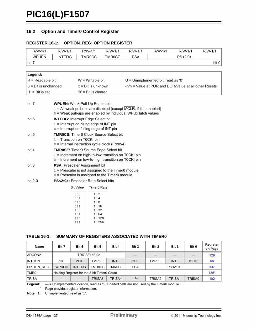
PIC16(L)F1507
16.2 Option and Timer0 Control Register
TABLE 16-1: SUMMARY OF REGISTERS ASSOCIATED WITH TIMER0
REGISTER 16-1: OPTION_REG: OPTION REGISTER
R/W-1/1 R/W-1/1 R/W-1/1 R/W-1/1 R/W-1/1 R/W-1/1 R/W-1/1 R/W-1/1
WPUEN INTEDG TMR0CS TMR0SE PSA PS<2:0>
bit 7 bit 0
Legend:
R = Readable bit W = Writable bit U = Unimplemented bit, read as ‘0’
u = Bit is unchanged x = Bit is unknown -n/n = Value at POR and BOR/Value at all other Resets
‘1’ = Bit is set ‘0’ = Bit is cleared
bit 7 WPUEN: Weak Pull-Up Enable bit1 = All weak pull-ups are disabled (except MCLR, if it is enabled)0 = Weak pull-ups are enabled by individual WPUx latch values
bit 6 INTEDG: Interrupt Edge Select bit1 = Interrupt on rising edge of INT pin0 = Interrupt on falling edge of INT pin
bit 5 TMR0CS: Timer0 Clock Source Select bit1 = Transition on T0CKI pin0 = Internal instruction cycle clock (FOSC/4)
bit 4 TMR0SE: Timer0 Source Edge Select bit1 = Increment on high-to-low transition on T0CKI pin0 = Increment on low-to-high transition on T0CKI pin
bit 3 PSA: Prescaler Assignment bit1 = Prescaler is not assigned to the Timer0 module0 = Prescaler is assigned to the Timer0 module
bit 2-0 PS<2:0>: Prescaler Rate Select bits
Name Bit 7 Bit 6 Bit 5 Bit 4 Bit 3 Bit 2 Bit 1 Bit 0Register on Page
ADCON2 TRIGSEL<3:0> — — — — 129
INTCON GIE PEIE TMR0IE INTE IOCIE TMR0IF INTF IOCIF 66
OPTION_REG WPUEN INTEDG TMR0CS TMR0SE PSA PS<2:0> 137
TMR0 Holding Register for the 8-bit Timer0 Count 135*
TRISA — — TRISA5 TRISA4 —(1) TRISA2 TRISA1 TRISA0 102
Legend: — = Unimplemented location, read as ‘0’. Shaded cells are not used by the Timer0 module.* Page provides register information.
Note 1: Unimplemented, read as ‘1’.
000001010011100101110111
1 : 21 : 41 : 81 : 161 : 321 : 641 : 1281 : 256
Bit Value Timer0 Rate
DS41586A-page 137 Preliminary 2011 Microchip Technology Inc.

PIC16(L)F1507
NOTES:
2011 Microchip Technology Inc. Preliminary DS41586A-page 138
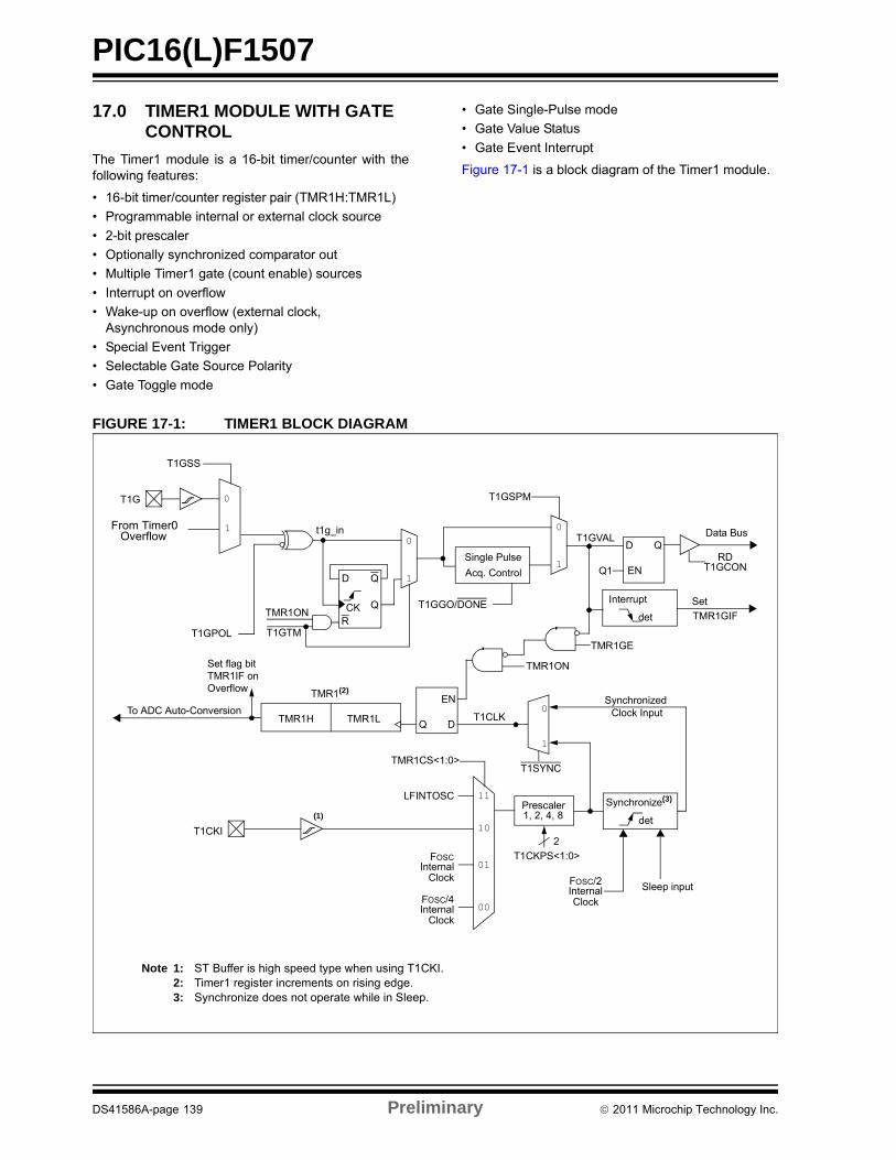
PIC16(L)F1507
17.0 TIMER1 MODULE WITH GATE CONTROL
The Timer1 module is a 16-bit timer/counter with thefollowing features:
• 16-bit timer/counter register pair (TMR1H:TMR1L)
• Programmable internal or external clock source
• 2-bit prescaler
• Optionally synchronized comparator out
• Multiple Timer1 gate (count enable) sources
• Interrupt on overflow
• Wake-up on overflow (external clock, Asynchronous mode only)
• Special Event Trigger
• Selectable Gate Source Polarity
• Gate Toggle mode
• Gate Single-Pulse mode
• Gate Value Status
• Gate Event Interrupt
Figure 17-1 is a block diagram of the Timer1 module.
FIGURE 17-1: TIMER1 BLOCK DIAGRAM
TMR1H TMR1L
T1SYNC
T1CKPS<1:0>
Prescaler1, 2, 4, 8
0
1
SynchronizedClock Input
2
Set flag bitTMR1IF onOverflow TMR1(2)
TMR1ON
Note 1: ST Buffer is high speed type when using T1CKI.2: Timer1 register increments on rising edge.3: Synchronize does not operate while in Sleep.
T1G
FOSC/4Internal
Clock
T1CKI
TMR1CS<1:0>
(1)
Synchronize(3)
det
Sleep input
TMR1GE
0
1
0
1
T1GPOL
D
QCK
Q
0
1
T1GVAL
T1GTM
Single Pulse
Acq. Control
T1GSPM
T1GGO/DONE
T1GSS
10
11
00
01FOSC
InternalClock
LFINTOSC
R
D
EN
Q
Q1RD
T1GCON
Data Bus
det
Interrupt
TMR1GIF
Set
T1CLK
FOSC/2InternalClock
D
EN
Q
t1g_in
TMR1ON
From Timer0 Overflow
To ADC Auto-Conversion
DS41586A-page 139 Preliminary 2011 Microchip Technology Inc.
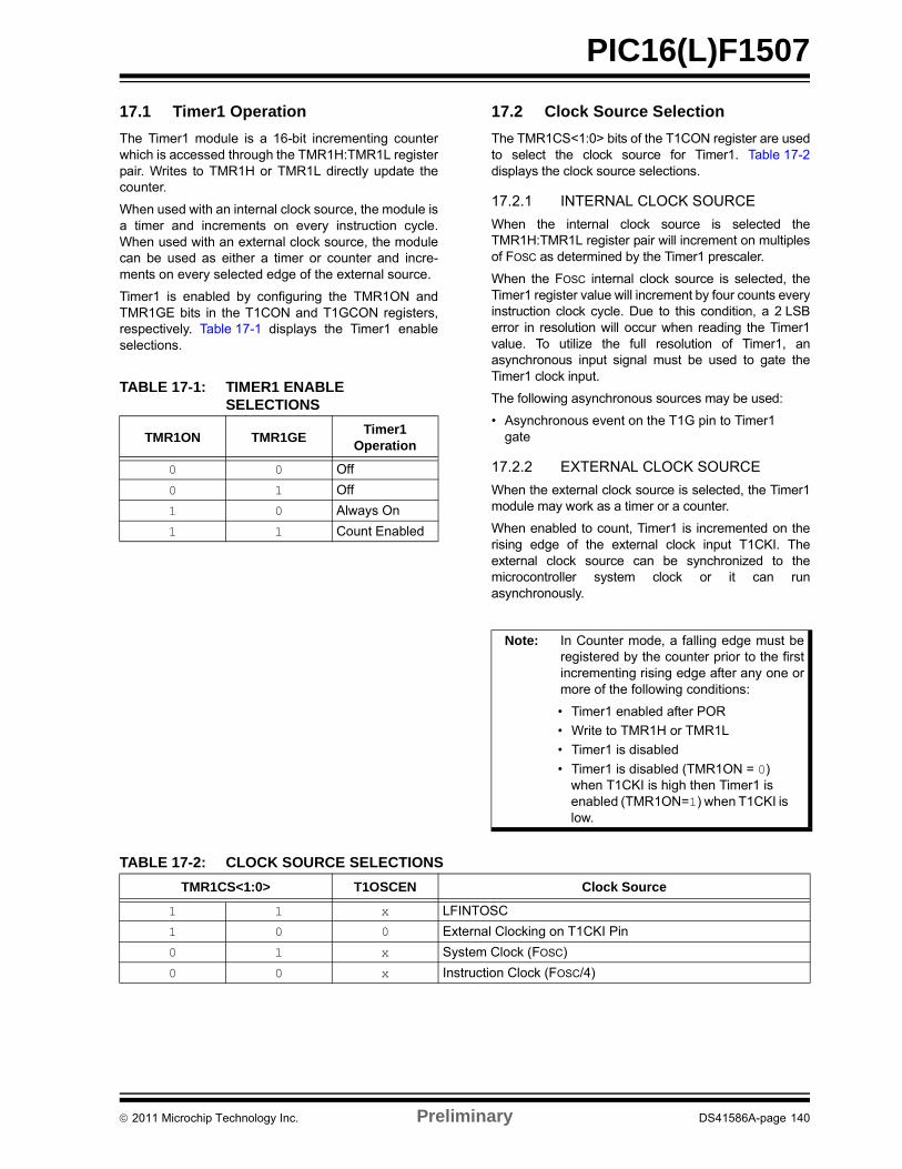
PIC16(L)F1507
17.1 Timer1 Operation
The Timer1 module is a 16-bit incrementing counterwhich is accessed through the TMR1H:TMR1L registerpair. Writes to TMR1H or TMR1L directly update thecounter.
When used with an internal clock source, the module isa timer and increments on every instruction cycle.When used with an external clock source, the modulecan be used as either a timer or counter and incre-ments on every selected edge of the external source.
Timer1 is enabled by configuring the TMR1ON andTMR1GE bits in the T1CON and T1GCON registers,respectively. Table 17-1 displays the Timer1 enableselections.
17.2 Clock Source Selection
The TMR1CS<1:0> bits of the T1CON register are usedto select the clock source for Timer1. Table 17-2displays the clock source selections.
17.2.1 INTERNAL CLOCK SOURCE
When the internal clock source is selected theTMR1H:TMR1L register pair will increment on multiplesof FOSC as determined by the Timer1 prescaler.
When the FOSC internal clock source is selected, theTimer1 register value will increment by four counts everyinstruction clock cycle. Due to this condition, a 2 LSBerror in resolution will occur when reading the Timer1value. To utilize the full resolution of Timer1, anasynchronous input signal must be used to gate theTimer1 clock input.
The following asynchronous sources may be used:
• Asynchronous event on the T1G pin to Timer1 gate
17.2.2 EXTERNAL CLOCK SOURCE
When the external clock source is selected, the Timer1module may work as a timer or a counter.
When enabled to count, Timer1 is incremented on therising edge of the external clock input T1CKI. Theexternal clock source can be synchronized to themicrocontroller system clock or it can runasynchronously.
TABLE 17-1: TIMER1 ENABLE SELECTIONS
TMR1ON TMR1GETimer1
Operation
0 0 Off
0 1 Off
1 0 Always On
1 1 Count Enabled
Note: In Counter mode, a falling edge must beregistered by the counter prior to the firstincrementing rising edge after any one ormore of the following conditions:
• Timer1 enabled after POR
• Write to TMR1H or TMR1L
• Timer1 is disabled
• Timer1 is disabled (TMR1ON = 0) when T1CKI is high then Timer1 is enabled (TMR1ON=1) when T1CKI is low.
TABLE 17-2: CLOCK SOURCE SELECTIONS
TMR1CS<1:0> T1OSCEN Clock Source
1 1 x LFINTOSC
1 0 0 External Clocking on T1CKI Pin
0 1 x System Clock (FOSC)
0 0 x Instruction Clock (FOSC/4)
2011 Microchip Technology Inc. Preliminary DS41586A-page 140
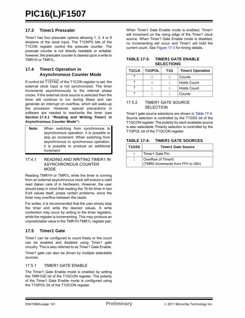
PIC16(L)F1507
17.3 Timer1 Prescaler
Timer1 has four prescaler options allowing 1, 2, 4 or 8divisions of the clock input. The T1CKPS bits of theT1CON register control the prescale counter. Theprescale counter is not directly readable or writable;however, the prescaler counter is cleared upon a write toTMR1H or TMR1L.
17.4 Timer1 Operation in Asynchronous Counter Mode
If control bit T1SYNC of the T1CON register is set, theexternal clock input is not synchronized. The timerincrements asynchronously to the internal phaseclocks. If the external clock source is selected then thetimer will continue to run during Sleep and cangenerate an interrupt on overflow, which will wake-upthe processor. However, special precautions insoftware are needed to read/write the timer (seeSection 17.4.1 “Reading and Writing Timer1 inAsynchronous Counter Mode”).
17.4.1 READING AND WRITING TIMER1 IN ASYNCHRONOUS COUNTER MODE
Reading TMR1H or TMR1L while the timer is runningfrom an external asynchronous clock will ensure a validread (taken care of in hardware). However, the usershould keep in mind that reading the 16-bit timer in two8-bit values itself, poses certain problems, since thetimer may overflow between the reads.
For writes, it is recommended that the user simply stopthe timer and write the desired values. A writecontention may occur by writing to the timer registers,while the register is incrementing. This may produce anunpredictable value in the TMR1H:TMR1L register pair.
17.5 Timer1 Gate
Timer1 can be configured to count freely or the countcan be enabled and disabled using Timer1 gatecircuitry. This is also referred to as Timer1 Gate Enable.
Timer1 gate can also be driven by multiple selectablesources.
17.5.1 TIMER1 GATE ENABLE
The Timer1 Gate Enable mode is enabled by settingthe TMR1GE bit of the T1GCON register. The polarityof the Timer1 Gate Enable mode is configured usingthe T1GPOL bit of the T1GCON register.
When Timer1 Gate Enable mode is enabled, Timer1will increment on the rising edge of the Timer1 clocksource. When Timer1 Gate Enable mode is disabled,no incrementing will occur and Timer1 will hold thecurrent count. See Figure 17-3 for timing details.
17.5.2 TIMER1 GATE SOURCE SELECTION
Timer1 gate source selections are shown in Table 17-4.Source selection is controlled by the T1GSS bit of theT1GCON register. The polarity for each available sourceis also selectable. Polarity selection is controlled by theT1GPOL bit of the T1GCON register.
TABLE 17-4: TIMER1 GATE SOURCES
Note: When switching from synchronous toasynchronous operation, it is possible toskip an increment. When switching fromasynchronous to synchronous operation,it is possible to produce an additionalincrement.
TABLE 17-3: TIMER1 GATE ENABLE SELECTIONS
T1CLK T1GPOL T1G Timer1 Operation
0 0 Counts
0 1 Holds Count
1 0 Holds Count
1 1 Counts
T1GSS Timer1 Gate Source
0 Timer1 Gate Pin
1 Overflow of Timer0(TMR0 increments from FFh to 00h)
DS41586A-page 141 Preliminary 2011 Microchip Technology Inc.
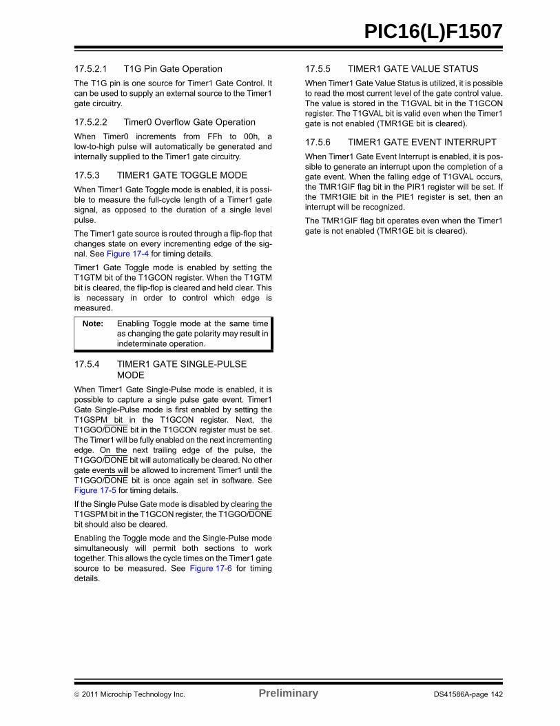
PIC16(L)F1507
17.5.2.1 T1G Pin Gate Operation
The T1G pin is one source for Timer1 Gate Control. Itcan be used to supply an external source to the Timer1gate circuitry.
17.5.2.2 Timer0 Overflow Gate Operation
When Timer0 increments from FFh to 00h, alow-to-high pulse will automatically be generated andinternally supplied to the Timer1 gate circuitry.
17.5.3 TIMER1 GATE TOGGLE MODE
When Timer1 Gate Toggle mode is enabled, it is possi-ble to measure the full-cycle length of a Timer1 gatesignal, as opposed to the duration of a single levelpulse.
The Timer1 gate source is routed through a flip-flop thatchanges state on every incrementing edge of the sig-nal. See Figure 17-4 for timing details.
Timer1 Gate Toggle mode is enabled by setting theT1GTM bit of the T1GCON register. When the T1GTMbit is cleared, the flip-flop is cleared and held clear. Thisis necessary in order to control which edge ismeasured.
17.5.4 TIMER1 GATE SINGLE-PULSE MODE
When Timer1 Gate Single-Pulse mode is enabled, it ispossible to capture a single pulse gate event. Timer1Gate Single-Pulse mode is first enabled by setting theT1GSPM bit in the T1GCON register. Next, theT1GGO/DONE bit in the T1GCON register must be set.The Timer1 will be fully enabled on the next incrementingedge. On the next trailing edge of the pulse, theT1GGO/DONE bit will automatically be cleared. No othergate events will be allowed to increment Timer1 until theT1GGO/DONE bit is once again set in software. SeeFigure 17-5 for timing details.
If the Single Pulse Gate mode is disabled by clearing theT1GSPM bit in the T1GCON register, the T1GGO/DONEbit should also be cleared.
Enabling the Toggle mode and the Single-Pulse modesimultaneously will permit both sections to worktogether. This allows the cycle times on the Timer1 gatesource to be measured. See Figure 17-6 for timingdetails.
17.5.5 TIMER1 GATE VALUE STATUS
When Timer1 Gate Value Status is utilized, it is possibleto read the most current level of the gate control value.The value is stored in the T1GVAL bit in the T1GCONregister. The T1GVAL bit is valid even when the Timer1gate is not enabled (TMR1GE bit is cleared).
17.5.6 TIMER1 GATE EVENT INTERRUPT
When Timer1 Gate Event Interrupt is enabled, it is pos-sible to generate an interrupt upon the completion of agate event. When the falling edge of T1GVAL occurs,the TMR1GIF flag bit in the PIR1 register will be set. Ifthe TMR1GIE bit in the PIE1 register is set, then aninterrupt will be recognized.
The TMR1GIF flag bit operates even when the Timer1gate is not enabled (TMR1GE bit is cleared).
Note: Enabling Toggle mode at the same timeas changing the gate polarity may result inindeterminate operation.
2011 Microchip Technology Inc. Preliminary DS41586A-page 142
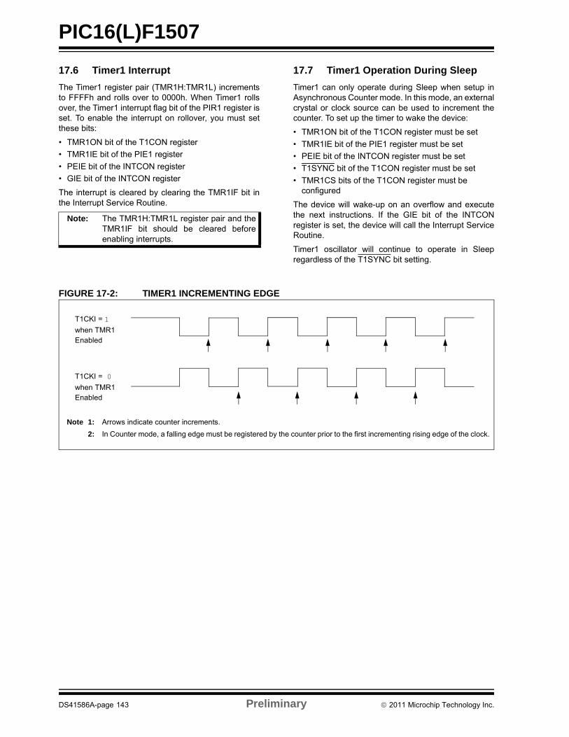
PIC16(L)F1507
17.6 Timer1 Interrupt
The Timer1 register pair (TMR1H:TMR1L) incrementsto FFFFh and rolls over to 0000h. When Timer1 rollsover, the Timer1 interrupt flag bit of the PIR1 register isset. To enable the interrupt on rollover, you must setthese bits:
• TMR1ON bit of the T1CON register
• TMR1IE bit of the PIE1 register
• PEIE bit of the INTCON register
• GIE bit of the INTCON register
The interrupt is cleared by clearing the TMR1IF bit inthe Interrupt Service Routine.
17.7 Timer1 Operation During Sleep
Timer1 can only operate during Sleep when setup inAsynchronous Counter mode. In this mode, an externalcrystal or clock source can be used to increment thecounter. To set up the timer to wake the device:
• TMR1ON bit of the T1CON register must be set
• TMR1IE bit of the PIE1 register must be set
• PEIE bit of the INTCON register must be set
• T1SYNC bit of the T1CON register must be set
• TMR1CS bits of the T1CON register must be configured
The device will wake-up on an overflow and executethe next instructions. If the GIE bit of the INTCONregister is set, the device will call the Interrupt ServiceRoutine.
Timer1 oscillator will continue to operate in Sleepregardless of the T1SYNC bit setting.
FIGURE 17-2: TIMER1 INCREMENTING EDGE
Note: The TMR1H:TMR1L register pair and theTMR1IF bit should be cleared beforeenabling interrupts.
T1CKI = 1
when TMR1Enabled
T1CKI = 0
when TMR1Enabled
Note 1: Arrows indicate counter increments.
2: In Counter mode, a falling edge must be registered by the counter prior to the first incrementing rising edge of the clock.
DS41586A-page 143 Preliminary 2011 Microchip Technology Inc.
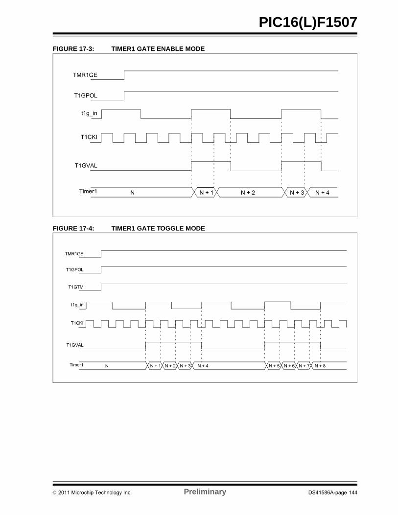
PIC16(L)F1507
FIGURE 17-3: TIMER1 GATE ENABLE MODE
FIGURE 17-4: TIMER1 GATE TOGGLE MODE
TMR1GE
T1GPOL
t1g_in
T1CKI
T1GVAL
Timer1 N N + 1 N + 2 N + 3 N + 4
TMR1GE
T1GPOL
T1GTM
t1g_in
T1CKI
T1GVAL
Timer1 N N + 1 N + 2 N + 3 N + 4 N + 5 N + 6 N + 7 N + 8
2011 Microchip Technology Inc. Preliminary DS41586A-page 144
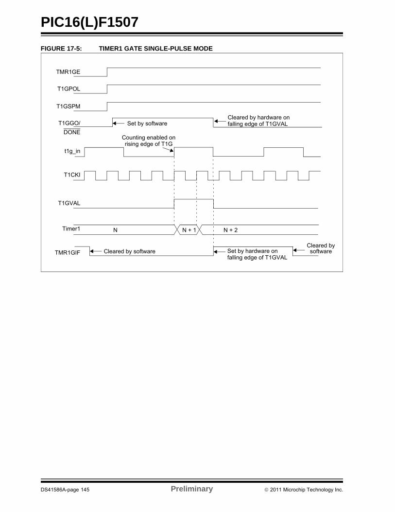
PIC16(L)F1507
FIGURE 17-5: TIMER1 GATE SINGLE-PULSE MODE
TMR1GE
T1GPOL
t1g_in
T1CKI
T1GVAL
Timer1 N N + 1 N + 2
T1GSPM
T1GGO/
DONE
Set by softwareCleared by hardware onfalling edge of T1GVAL
Set by hardware onfalling edge of T1GVAL
Cleared by softwareCleared bysoftwareTMR1GIF
Counting enabled onrising edge of T1G
DS41586A-page 145 Preliminary 2011 Microchip Technology Inc.
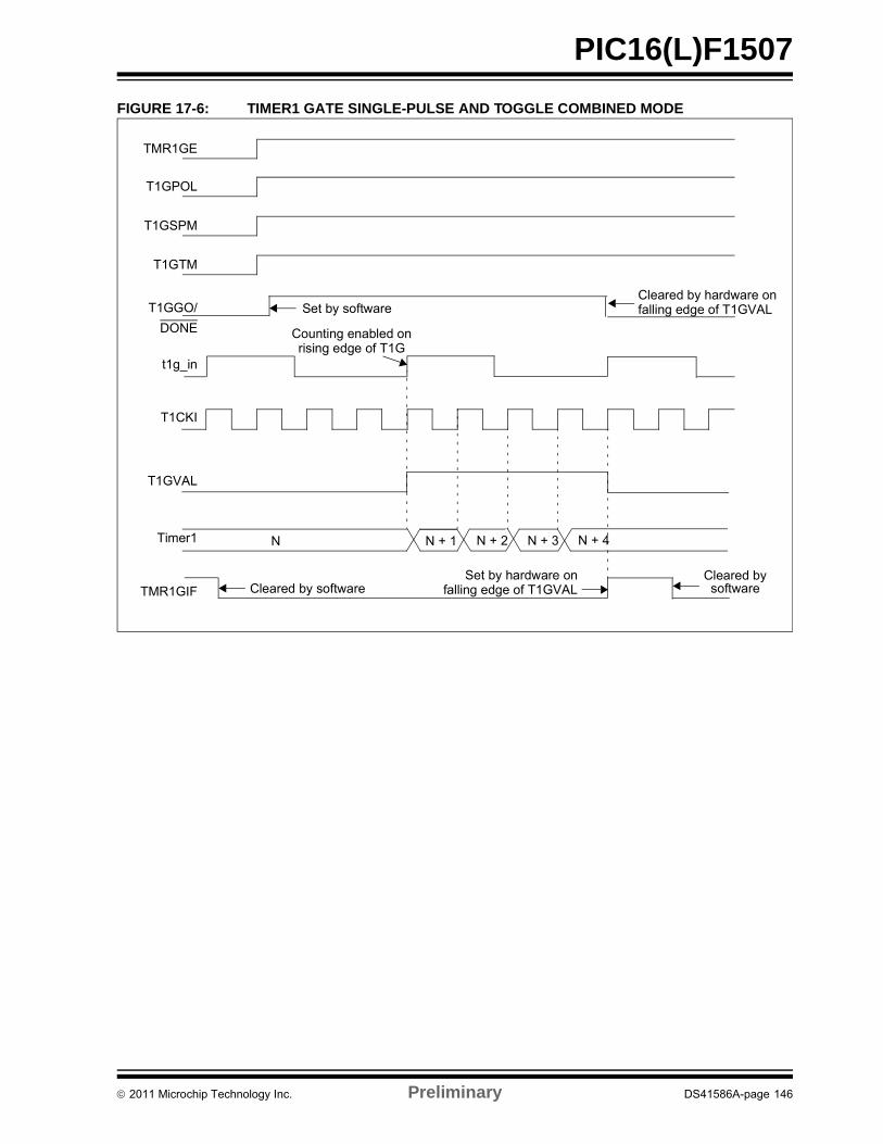
PIC16(L)F1507
FIGURE 17-6: TIMER1 GATE SINGLE-PULSE AND TOGGLE COMBINED MODE
TMR1GE
T1GPOL
t1g_in
T1CKI
T1GVAL
Timer1 N N + 1 N + 2
T1GSPM
T1GGO/
DONE
Set by softwareCleared by hardware onfalling edge of T1GVAL
Set by hardware onfalling edge of T1GVALCleared by software
Cleared bysoftwareTMR1GIF
T1GTM
Counting enabled onrising edge of T1G
N + 4N + 3
2011 Microchip Technology Inc. Preliminary DS41586A-page 146
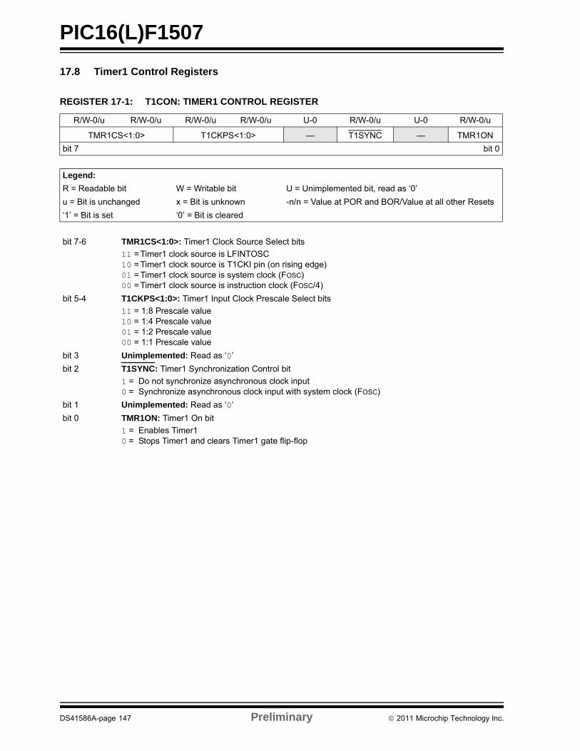
PIC16(L)F1507
17.8 Timer1 Control Registers
REGISTER 17-1: T1CON: TIMER1 CONTROL REGISTER
R/W-0/u R/W-0/u R/W-0/u R/W-0/u U-0 R/W-0/u U-0 R/W-0/u
TMR1CS<1:0> T1CKPS<1:0> — T1SYNC — TMR1ON
bit 7 bit 0
Legend:
R = Readable bit W = Writable bit U = Unimplemented bit, read as ‘0’
u = Bit is unchanged x = Bit is unknown -n/n = Value at POR and BOR/Value at all other Resets
‘1’ = Bit is set ‘0’ = Bit is cleared
bit 7-6 TMR1CS<1:0>: Timer1 Clock Source Select bits
11 = Timer1 clock source is LFINTOSC10 = Timer1 clock source is T1CKI pin (on rising edge)01 = Timer1 clock source is system clock (FOSC)00 = Timer1 clock source is instruction clock (FOSC/4)
bit 5-4 T1CKPS<1:0>: Timer1 Input Clock Prescale Select bits
11 = 1:8 Prescale value10 = 1:4 Prescale value01 = 1:2 Prescale value00 = 1:1 Prescale value
bit 3 Unimplemented: Read as ‘0’
bit 2 T1SYNC: Timer1 Synchronization Control bit
1 = Do not synchronize asynchronous clock input0 = Synchronize asynchronous clock input with system clock (FOSC)
bit 1 Unimplemented: Read as ‘0’
bit 0 TMR1ON: Timer1 On bit
1 = Enables Timer10 = Stops Timer1 and clears Timer1 gate flip-flop
DS41586A-page 147 Preliminary 2011 Microchip Technology Inc.
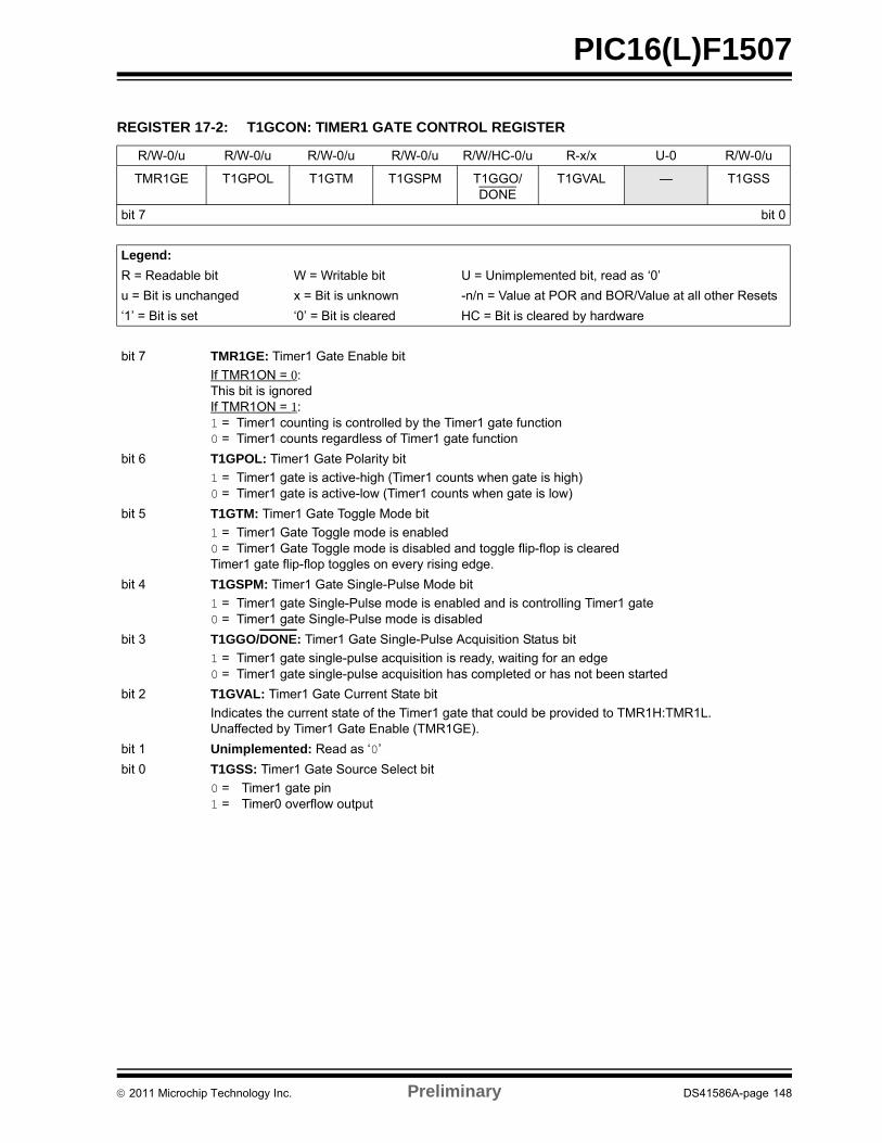
PIC16(L)F1507
REGISTER 17-2: T1GCON: TIMER1 GATE CONTROL REGISTER
R/W-0/u R/W-0/u R/W-0/u R/W-0/u R/W/HC-0/u R-x/x U-0 R/W-0/u
TMR1GE T1GPOL T1GTM T1GSPM T1GGO/DONE
T1GVAL — T1GSS
bit 7 bit 0
Legend:
R = Readable bit W = Writable bit U = Unimplemented bit, read as ‘0’
u = Bit is unchanged x = Bit is unknown -n/n = Value at POR and BOR/Value at all other Resets
‘1’ = Bit is set ‘0’ = Bit is cleared HC = Bit is cleared by hardware
bit 7 TMR1GE: Timer1 Gate Enable bit
If TMR1ON = 0:This bit is ignoredIf TMR1ON = 1:1 = Timer1 counting is controlled by the Timer1 gate function0 = Timer1 counts regardless of Timer1 gate function
bit 6 T1GPOL: Timer1 Gate Polarity bit
1 = Timer1 gate is active-high (Timer1 counts when gate is high)0 = Timer1 gate is active-low (Timer1 counts when gate is low)
bit 5 T1GTM: Timer1 Gate Toggle Mode bit
1 = Timer1 Gate Toggle mode is enabled0 = Timer1 Gate Toggle mode is disabled and toggle flip-flop is clearedTimer1 gate flip-flop toggles on every rising edge.
bit 4 T1GSPM: Timer1 Gate Single-Pulse Mode bit
1 = Timer1 gate Single-Pulse mode is enabled and is controlling Timer1 gate0 = Timer1 gate Single-Pulse mode is disabled
bit 3 T1GGO/DONE: Timer1 Gate Single-Pulse Acquisition Status bit
1 = Timer1 gate single-pulse acquisition is ready, waiting for an edge0 = Timer1 gate single-pulse acquisition has completed or has not been started
bit 2 T1GVAL: Timer1 Gate Current State bit
Indicates the current state of the Timer1 gate that could be provided to TMR1H:TMR1L.Unaffected by Timer1 Gate Enable (TMR1GE).
bit 1 Unimplemented: Read as ‘0’
bit 0 T1GSS: Timer1 Gate Source Select bit
0 = Timer1 gate pin1 = Timer0 overflow output
2011 Microchip Technology Inc. Preliminary DS41586A-page 148
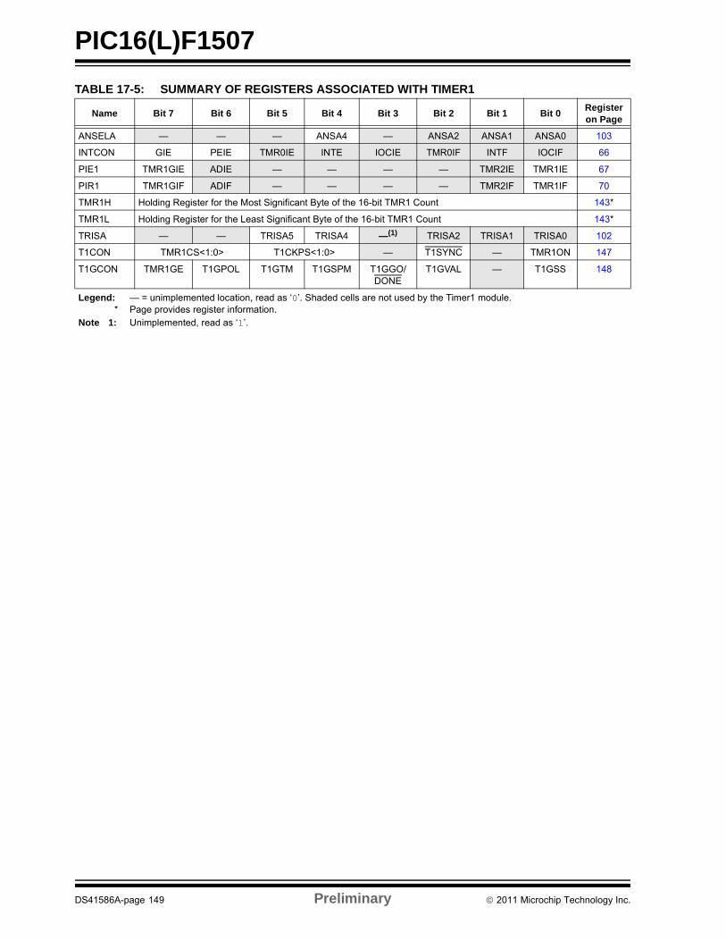
PIC16(L)F1507
TABLE 17-5: SUMMARY OF REGISTERS ASSOCIATED WITH TIMER1
Name Bit 7 Bit 6 Bit 5 Bit 4 Bit 3 Bit 2 Bit 1 Bit 0Register on Page
ANSELA — — — ANSA4 — ANSA2 ANSA1 ANSA0 103
INTCON GIE PEIE TMR0IE INTE IOCIE TMR0IF INTF IOCIF 66
PIE1 TMR1GIE ADIE — — — — TMR2IE TMR1IE 67
PIR1 TMR1GIF ADIF — — — — TMR2IF TMR1IF 70
TMR1H Holding Register for the Most Significant Byte of the 16-bit TMR1 Count 143*
TMR1L Holding Register for the Least Significant Byte of the 16-bit TMR1 Count 143*
TRISA — — TRISA5 TRISA4 —(1) TRISA2 TRISA1 TRISA0 102
T1CON TMR1CS<1:0> T1CKPS<1:0> — T1SYNC — TMR1ON 147
T1GCON TMR1GE T1GPOL T1GTM T1GSPM T1GGO/DONE
T1GVAL — T1GSS 148
Legend: — = unimplemented location, read as ‘0’. Shaded cells are not used by the Timer1 module.* Page provides register information.
Note 1: Unimplemented, read as ‘1’.
DS41586A-page 149 Preliminary 2011 Microchip Technology Inc.

PIC16(L)F1507
NOTES:
2011 Microchip Technology Inc. Preliminary DS41586A-page 150

PIC16(L)F1507
18.0 TIMER2 MODULE
The Timer2 module incorporates the following features:
• 8-bit Timer and Period registers (TMR2 and PR2, respectively)
• Readable and writable (both registers)
• Software programmable prescaler (1:1, 1:4, 1:16, and 1:64)
• Software programmable postscaler (1:1 to 1:16)
• Interrupt on TMR2 match with PR2, respectively
• Optional use as the shift clock for the MSSP modules
See Figure 18-1 for a block diagram of Timer2.
FIGURE 18-1: TIMER2 BLOCK DIAGRAM
Comparator
TMR2Sets Flag
TMR2
Output
Reset
Postscaler
Prescaler
PR2
2
FOSC/4
1:1 to 1:16
1:1, 1:4, 1:16, 1:64
EQ
4
bit TMR2IF
T2OUTPS<3:0>
T2CKPS<1:0>
DS41586A-page 151 Preliminary 2011 Microchip Technology Inc.
PIC16(L)F1507
18.1 Timer2 Operation
The clock input to the Timer2 module is the systeminstruction clock (FOSC/4).
TMR2 increments from 00h on each clock edge.
A 4-bit counter/prescaler on the clock input allows directinput, divide-by-4 and divide-by-16 prescale options.These options are selected by the prescaler control bits,T2CKPS<1:0> of the T2CON register. The value ofTMR2 is compared to that of the Period register, PR2, oneach clock cycle. When the two values match, thecomparator generates a match signal as the timeroutput. This signal also resets the value of TMR2 to 00hon the next cycle and drives the outputcounter/postscaler (see Section 18.2 “Timer2Interrupt”).
The TMR2 and PR2 registers are both directly readableand writable. The TMR2 register is cleared on anydevice Reset, whereas the PR2 register initializes toFFh. Both the prescaler and postscaler counters arecleared on the following events:
• a write to the TMR2 register
• a write to the T2CON register
• Power-on Reset (POR)
• Brown-out Reset (BOR)
• MCLR Reset
• Watchdog Timer (WDT) Reset
• Stack Overflow Reset
• Stack Underflow Reset
• RESET Instruction
18.2 Timer2 Interrupt
Timer2 can also generate an optional device interrupt.The Timer2 output signal (TMR2-to-PR2 match)provides the input for the 4-bit counter/postscaler. Thiscounter generates the TMR2 match interrupt flag whichis latched in TMR2IF of the PIR1 register. The interruptis enabled by setting the TMR2 Match Interrupt Enablebit, TMR2IE of the PIE1 register.
A range of 16 postscale options (from 1:1 through 1:16inclusive) can be selected with the postscaler controlbits, T2OUTPS<3:0>, of the T2CON register.
18.3 Timer2 Output
The unscaled output of TMR2 is available primarily tothe PWMx module, where it is used as a time base foroperation.
18.4 Timer2 Operation During Sleep
Timer2 cannot be operated while the processor is inSleep mode. The contents of the TMR2 and PR2registers will remain unchanged while the processor isin Sleep mode.
Note: TMR2 is not cleared when T2CON iswritten.
2011 Microchip Technology Inc. Preliminary DS41586A-page 152
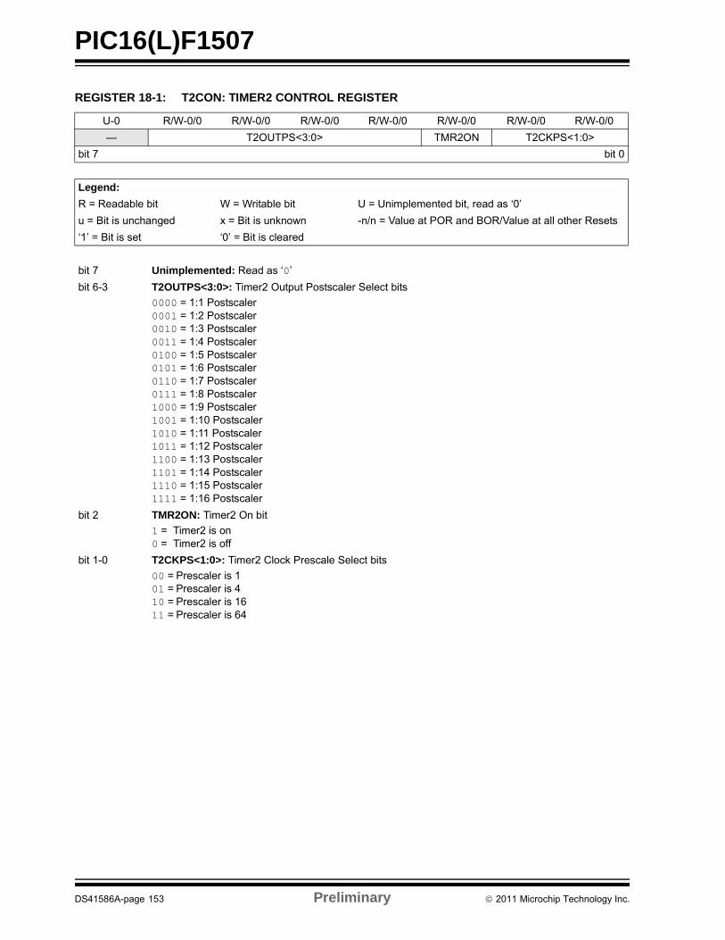
PIC16(L)F1507
REGISTER 18-1: T2CON: TIMER2 CONTROL REGISTER
U-0 R/W-0/0 R/W-0/0 R/W-0/0 R/W-0/0 R/W-0/0 R/W-0/0 R/W-0/0
— T2OUTPS<3:0> TMR2ON T2CKPS<1:0>
bit 7 bit 0
Legend:
R = Readable bit W = Writable bit U = Unimplemented bit, read as ‘0’
u = Bit is unchanged x = Bit is unknown -n/n = Value at POR and BOR/Value at all other Resets
‘1’ = Bit is set ‘0’ = Bit is cleared
bit 7 Unimplemented: Read as ‘0’
bit 6-3 T2OUTPS<3:0>: Timer2 Output Postscaler Select bits
0000 = 1:1 Postscaler0001 = 1:2 Postscaler0010 = 1:3 Postscaler0011 = 1:4 Postscaler0100 = 1:5 Postscaler0101 = 1:6 Postscaler0110 = 1:7 Postscaler0111 = 1:8 Postscaler1000 = 1:9 Postscaler1001 = 1:10 Postscaler1010 = 1:11 Postscaler1011 = 1:12 Postscaler1100 = 1:13 Postscaler1101 = 1:14 Postscaler1110 = 1:15 Postscaler1111 = 1:16 Postscaler
bit 2 TMR2ON: Timer2 On bit
1 = Timer2 is on0 = Timer2 is off
bit 1-0 T2CKPS<1:0>: Timer2 Clock Prescale Select bits
00 = Prescaler is 101 = Prescaler is 410 = Prescaler is 1611 = Prescaler is 64
DS41586A-page 153 Preliminary 2011 Microchip Technology Inc.
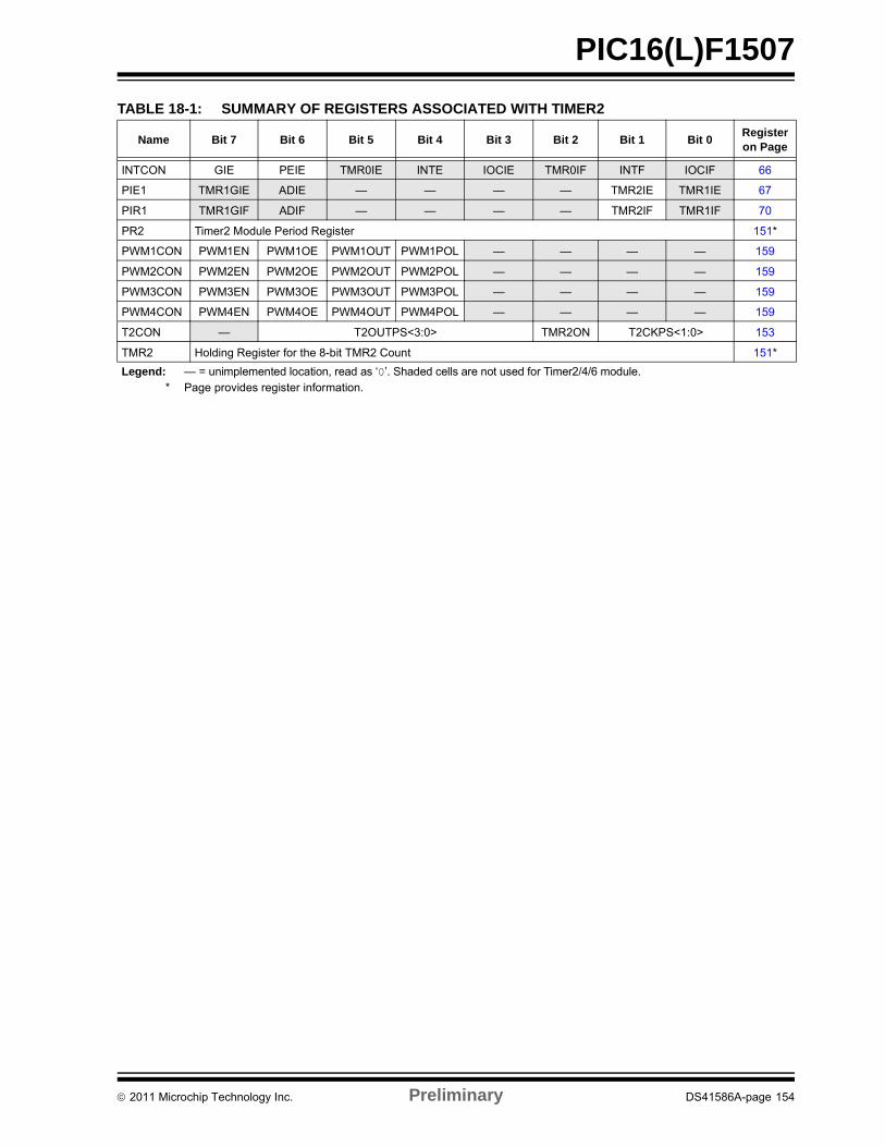
PIC16(L)F1507
TABLE 18-1: SUMMARY OF REGISTERS ASSOCIATED WITH TIMER2
Name Bit 7 Bit 6 Bit 5 Bit 4 Bit 3 Bit 2 Bit 1 Bit 0Register on Page
INTCON GIE PEIE TMR0IE INTE IOCIE TMR0IF INTF IOCIF 66
PIE1 TMR1GIE ADIE — — — — TMR2IE TMR1IE 67
PIR1 TMR1GIF ADIF — — — — TMR2IF TMR1IF 70
PR2 Timer2 Module Period Register 151*
PWM1CON PWM1EN PWM1OE PWM1OUT PWM1POL — — — — 159
PWM2CON PWM2EN PWM2OE PWM2OUT PWM2POL — — — — 159
PWM3CON PWM3EN PWM3OE PWM3OUT PWM3POL — — — — 159
PWM4CON PWM4EN PWM4OE PWM4OUT PWM4POL — — — — 159
T2CON — T2OUTPS<3:0> TMR2ON T2CKPS<1:0> 153
TMR2 Holding Register for the 8-bit TMR2 Count 151*
Legend: — = unimplemented location, read as ‘0’. Shaded cells are not used for Timer2/4/6 module.* Page provides register information.
2011 Microchip Technology Inc. Preliminary DS41586A-page 154
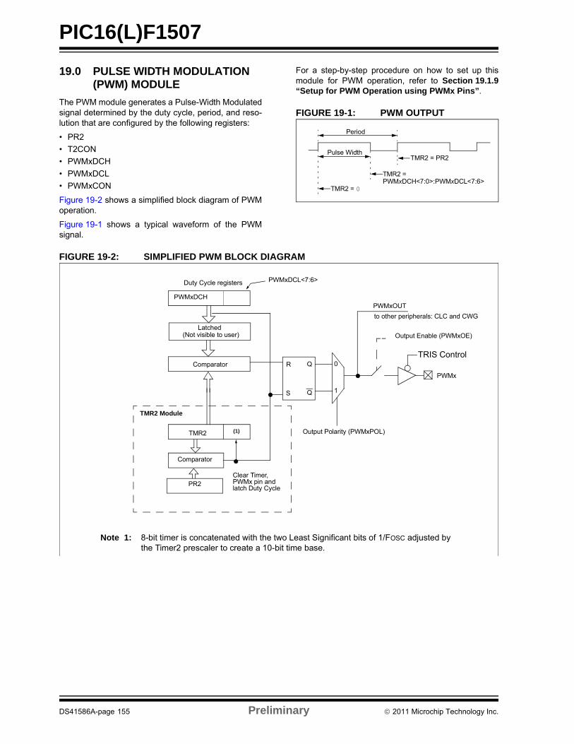
PIC16(L)F1507
19.0 PULSE WIDTH MODULATION (PWM) MODULE
The PWM module generates a Pulse-Width Modulatedsignal determined by the duty cycle, period, and reso-lution that are configured by the following registers:
• PR2
• T2CON
• PWMxDCH
• PWMxDCL
• PWMxCON
Figure 19-2 shows a simplified block diagram of PWMoperation.
Figure 19-1 shows a typical waveform of the PWMsignal.
For a step-by-step procedure on how to set up thismodule for PWM operation, refer to Section 19.1.9“Setup for PWM Operation using PWMx Pins”.
FIGURE 19-1: PWM OUTPUT
FIGURE 19-2: SIMPLIFIED PWM BLOCK DIAGRAM
Period
Pulse Width
TMR2 = 0
TMR2 =
TMR2 = PR2
PWMxDCH<7:0>:PWMxDCL<7:6>
PWMxDCH
Comparator
TMR2
Comparator
PR2
(1)
R Q
S
Duty Cycle registers PWMxDCL<7:6>
Clear Timer,PWMx pin and latch Duty Cycle
Note 1: 8-bit timer is concatenated with the two Least Significant bits of 1/FOSC adjusted by the Timer2 prescaler to create a 10-bit time base.
Latched(Not visible to user)
Q
Output Polarity (PWMxPOL)
TMR2 Module
0
1
PWMxOUT
to other peripherals: CLC and CWG
PWMx
Output Enable (PWMxOE)
TRIS Control
DS41586A-page 155 Preliminary 2011 Microchip Technology Inc.
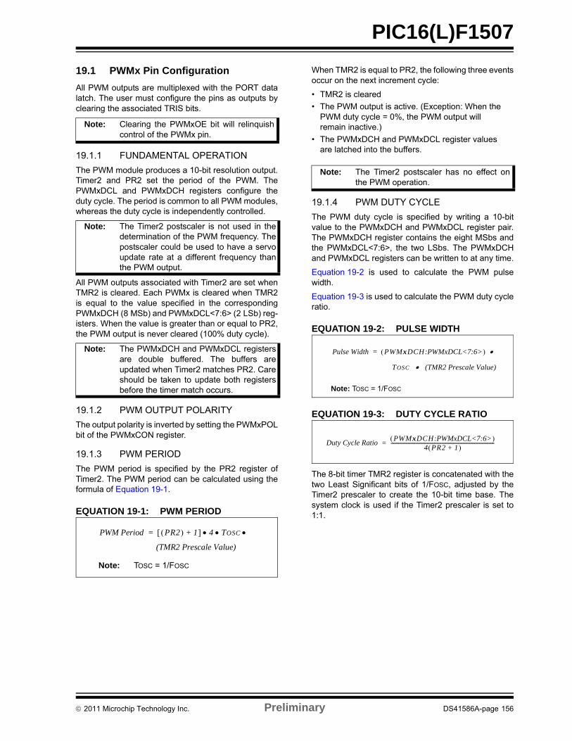
PIC16(L)F1507
19.1 PWMx Pin Configuration
All PWM outputs are multiplexed with the PORT datalatch. The user must configure the pins as outputs byclearing the associated TRIS bits.
19.1.1 FUNDAMENTAL OPERATION
The PWM module produces a 10-bit resolution output.Timer2 and PR2 set the period of the PWM. ThePWMxDCL and PWMxDCH registers configure theduty cycle. The period is common to all PWM modules,whereas the duty cycle is independently controlled.
All PWM outputs associated with Timer2 are set whenTMR2 is cleared. Each PWMx is cleared when TMR2is equal to the value specified in the correspondingPWMxDCH (8 MSb) and PWMxDCL<7:6> (2 LSb) reg-isters. When the value is greater than or equal to PR2,the PWM output is never cleared (100% duty cycle).
19.1.2 PWM OUTPUT POLARITY
The output polarity is inverted by setting the PWMxPOLbit of the PWMxCON register.
19.1.3 PWM PERIOD
The PWM period is specified by the PR2 register ofTimer2. The PWM period can be calculated using theformula of Equation 19-1.
EQUATION 19-1: PWM PERIOD
When TMR2 is equal to PR2, the following three eventsoccur on the next increment cycle:
• TMR2 is cleared
• The PWM output is active. (Exception: When the PWM duty cycle = 0%, the PWM output will remain inactive.)
• The PWMxDCH and PWMxDCL register values are latched into the buffers.
19.1.4 PWM DUTY CYCLE
The PWM duty cycle is specified by writing a 10-bitvalue to the PWMxDCH and PWMxDCL register pair.The PWMxDCH register contains the eight MSbs andthe PWMxDCL<7:6>, the two LSbs. The PWMxDCHand PWMxDCL registers can be written to at any time.
Equation 19-2 is used to calculate the PWM pulsewidth.
Equation 19-3 is used to calculate the PWM duty cycleratio.
EQUATION 19-2: PULSE WIDTH
EQUATION 19-3: DUTY CYCLE RATIO
The 8-bit timer TMR2 register is concatenated with thetwo Least Significant bits of 1/FOSC, adjusted by theTimer2 prescaler to create the 10-bit time base. Thesystem clock is used if the Timer2 prescaler is set to1:1.
Note: Clearing the PWMxOE bit will relinquishcontrol of the PWMx pin.
Note: The Timer2 postscaler is not used in thedetermination of the PWM frequency. Thepostscaler could be used to have a servoupdate rate at a different frequency thanthe PWM output.
Note: The PWMxDCH and PWMxDCL registersare double buffered. The buffers areupdated when Timer2 matches PR2. Careshould be taken to update both registersbefore the timer match occurs.
PWM Period PR2 1+ 4 TOSC =
(TMR2 Prescale Value)
Note: TOSC = 1/FOSC
Note: The Timer2 postscaler has no effect onthe PWM operation.
Pulse Width PWMxDCH:PWMxDCL<7:6> =
TOSC (TMR2 Prescale Value)
Note: TOSC = 1/FOSC
Duty Cycle RatioPWMxDCH:PWMxDCL<7:6>
4 PR2 1+ -----------------------------------------------------------------------------------=
2011 Microchip Technology Inc. Preliminary DS41586A-page 156
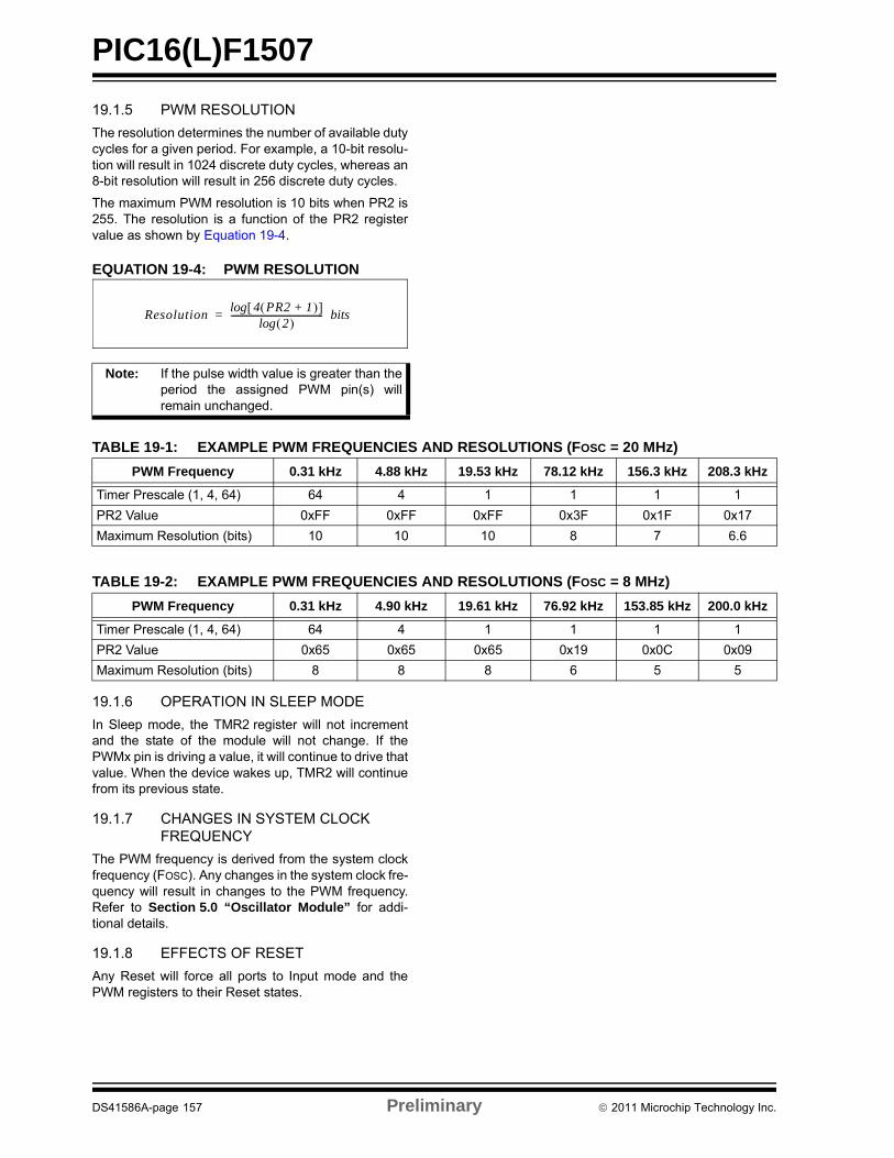
PIC16(L)F1507
19.1.5 PWM RESOLUTION
The resolution determines the number of available dutycycles for a given period. For example, a 10-bit resolu-tion will result in 1024 discrete duty cycles, whereas an8-bit resolution will result in 256 discrete duty cycles.
The maximum PWM resolution is 10 bits when PR2 is255. The resolution is a function of the PR2 registervalue as shown by Equation 19-4.
EQUATION 19-4: PWM RESOLUTION
19.1.6 OPERATION IN SLEEP MODE
In Sleep mode, the TMR2 register will not incrementand the state of the module will not change. If thePWMx pin is driving a value, it will continue to drive thatvalue. When the device wakes up, TMR2 will continuefrom its previous state.
19.1.7 CHANGES IN SYSTEM CLOCK FREQUENCY
The PWM frequency is derived from the system clockfrequency (FOSC). Any changes in the system clock fre-quency will result in changes to the PWM frequency.Refer to Section 5.0 “Oscillator Module” for addi-tional details.
19.1.8 EFFECTS OF RESET
Any Reset will force all ports to Input mode and thePWM registers to their Reset states.
Note: If the pulse width value is greater than theperiod the assigned PWM pin(s) willremain unchanged.
Resolution4 PR2 1+ log
2 log------------------------------------------ bits=
TABLE 19-1: EXAMPLE PWM FREQUENCIES AND RESOLUTIONS (FOSC = 20 MHz)
PWM Frequency 0.31 kHz 4.88 kHz 19.53 kHz 78.12 kHz 156.3 kHz 208.3 kHz
Timer Prescale (1, 4, 64) 64 4 1 1 1 1
PR2 Value 0xFF 0xFF 0xFF 0x3F 0x1F 0x17
Maximum Resolution (bits) 10 10 10 8 7 6.6
TABLE 19-2: EXAMPLE PWM FREQUENCIES AND RESOLUTIONS (FOSC = 8 MHz)
PWM Frequency 0.31 kHz 4.90 kHz 19.61 kHz 76.92 kHz 153.85 kHz 200.0 kHz
Timer Prescale (1, 4, 64) 64 4 1 1 1 1
PR2 Value 0x65 0x65 0x65 0x19 0x0C 0x09
Maximum Resolution (bits) 8 8 8 6 5 5
DS41586A-page 157 Preliminary 2011 Microchip Technology Inc.
PIC16(L)F1507
19.1.9 SETUP FOR PWM OPERATION USING PWMx PINS
The following steps should be taken when configuringthe module for PWM operation using the PWMx pins:
1. Disable the PWMx pin output driver(s) by settingthe associated TRIS bit(s).
2. Clear the PWMxCON register.
3. Load the PR2 register with the PWM periodvalue.
4. Clear the PWMxDCH register and bits <7:6> ofthe PWMxDCL register.
5. Configure and start Timer2:
• Clear the TMR2IF interrupt flag bit of the PIR1 register. See Note below.
• Configure the T2CKPS bits of the T2CON register with the Timer2 prescale value.
• Enable Timer2 by setting the TMR2ON bit of the T2CON register.
6. Enable PWM output pin and wait until Timer2overflows, TMR2IF bit of the PIR1 register is set.See note below.
7. Enable the PWMx pin output driver(s) by clear-ing the associated TRIS bit(s) and setting thePWMxOE bit of the PWMxCON register.
8. Configure the PWM module by loading thePWMxCON register with the appropriate values.
Note 1: In order to send a complete duty cycleand period on the first PWM output, theabove steps must be followed in the ordergiven. If it is not critical to start with acomplete PWM signal, then move Step 8to replace Step 4.
2: For operation with other peripherals only,disable PWMx pin outputs.
2011 Microchip Technology Inc. Preliminary DS41586A-page 158
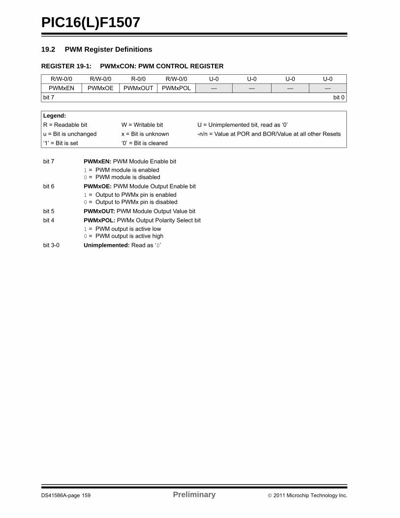
PIC16(L)F1507
19.2 PWM Register Definitions
REGISTER 19-1: PWMxCON: PWM CONTROL REGISTER
R/W-0/0 R/W-0/0 R-0/0 R/W-0/0 U-0 U-0 U-0 U-0
PWMxEN PWMxOE PWMxOUT PWMxPOL — — — —
bit 7 bit 0
Legend:
R = Readable bit W = Writable bit U = Unimplemented bit, read as ‘0’
u = Bit is unchanged x = Bit is unknown -n/n = Value at POR and BOR/Value at all other Resets
‘1’ = Bit is set ‘0’ = Bit is cleared
bit 7 PWMxEN: PWM Module Enable bit
1 = PWM module is enabled0 = PWM module is disabled
bit 6 PWMxOE: PWM Module Output Enable bit
1 = Output to PWMx pin is enabled0 = Output to PWMx pin is disabled
bit 5 PWMxOUT: PWM Module Output Value bit
bit 4 PWMxPOL: PWMx Output Polarity Select bit
1 = PWM output is active low0 = PWM output is active high
bit 3-0 Unimplemented: Read as ‘0’
DS41586A-page 159 Preliminary 2011 Microchip Technology Inc.
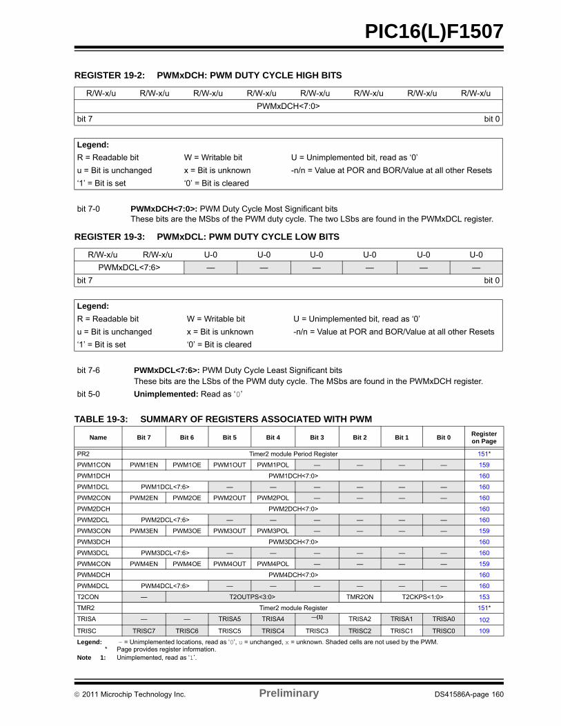
PIC16(L)F1507
REGISTER 19-2: PWMxDCH: PWM DUTY CYCLE HIGH BITS
R/W-x/u R/W-x/u R/W-x/u R/W-x/u R/W-x/u R/W-x/u R/W-x/u R/W-x/u
PWMxDCH<7:0>
bit 7 bit 0
Legend:
R = Readable bit W = Writable bit U = Unimplemented bit, read as ‘0’
u = Bit is unchanged x = Bit is unknown -n/n = Value at POR and BOR/Value at all other Resets
‘1’ = Bit is set ‘0’ = Bit is cleared
bit 7-0 PWMxDCH<7:0>: PWM Duty Cycle Most Significant bitsThese bits are the MSbs of the PWM duty cycle. The two LSbs are found in the PWMxDCL register.
REGISTER 19-3: PWMxDCL: PWM DUTY CYCLE LOW BITS
R/W-x/u R/W-x/u U-0 U-0 U-0 U-0 U-0 U-0
PWMxDCL<7:6> — — — — — —
bit 7 bit 0
Legend:
R = Readable bit W = Writable bit U = Unimplemented bit, read as ‘0’
u = Bit is unchanged x = Bit is unknown -n/n = Value at POR and BOR/Value at all other Resets
‘1’ = Bit is set ‘0’ = Bit is cleared
bit 7-6 PWMxDCL<7:6>: PWM Duty Cycle Least Significant bitsThese bits are the LSbs of the PWM duty cycle. The MSbs are found in the PWMxDCH register.
bit 5-0 Unimplemented: Read as ‘0’
TABLE 19-3: SUMMARY OF REGISTERS ASSOCIATED WITH PWM
Name Bit 7 Bit 6 Bit 5 Bit 4 Bit 3 Bit 2 Bit 1 Bit 0Register on Page
PR2 Timer2 module Period Register 151*
PWM1CON PWM1EN PWM1OE PWM1OUT PWM1POL — — — — 159
PWM1DCH PWM1DCH<7:0> 160
PWM1DCL PWM1DCL<7:6> — — — — — — 160
PWM2CON PWM2EN PWM2OE PWM2OUT PWM2POL — — — — 160
PWM2DCH PWM2DCH<7:0> 160
PWM2DCL PWM2DCL<7:6> — — — — — — 160
PWM3CON PWM3EN PWM3OE PWM3OUT PWM3POL — — — — 159
PWM3DCH PWM3DCH<7:0> 160
PWM3DCL PWM3DCL<7:6> — — — — — — 160
PWM4CON PWM4EN PWM4OE PWM4OUT PWM4POL — — — — 159
PWM4DCH PWM4DCH<7:0> 160
PWM4DCL PWM4DCL<7:6> — — — — — — 160
T2CON — T2OUTPS<3:0> TMR2ON T2CKPS<1:0> 153
TMR2 Timer2 module Register 151*
TRISA — — TRISA5 TRISA4 —(1) TRISA2 TRISA1 TRISA0 102
TRISC TRISC7 TRISC6 TRISC5 TRISC4 TRISC3 TRISC2 TRISC1 TRISC0 109
Legend: - = Unimplemented locations, read as ‘0’, u = unchanged, x = unknown. Shaded cells are not used by the PWM.* Page provides register information.
Note 1: Unimplemented, read as ‘1’.
2011 Microchip Technology Inc. Preliminary DS41586A-page 160
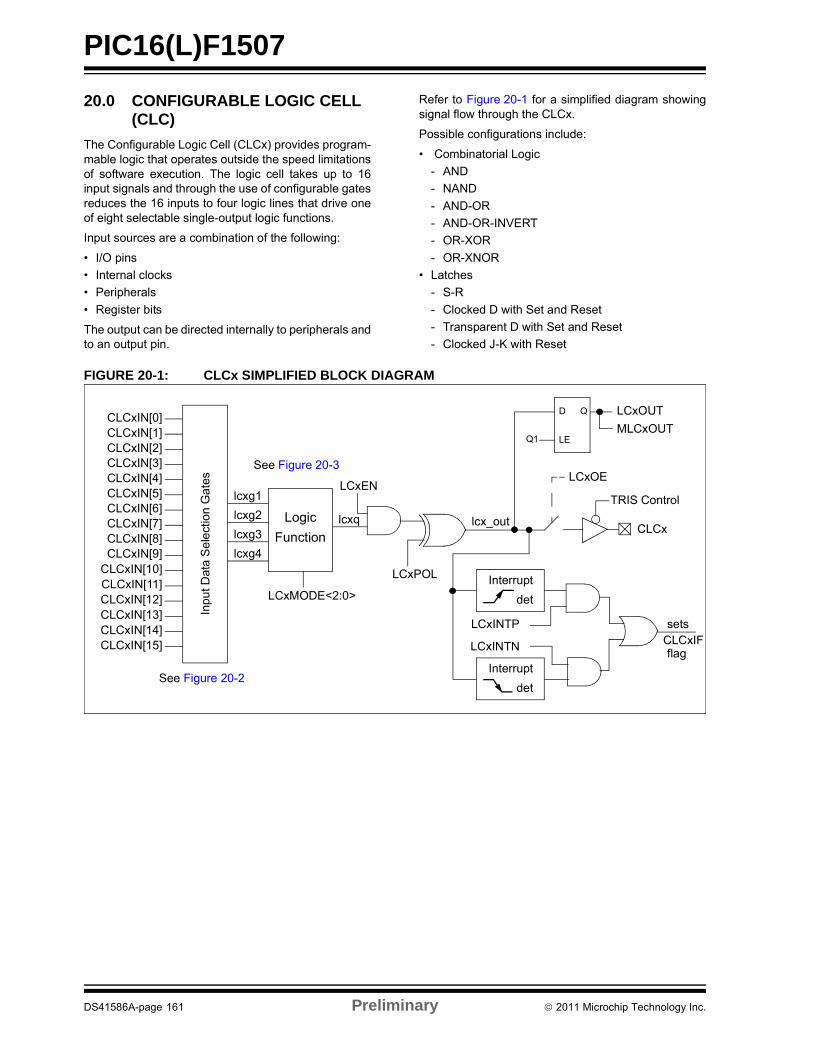
PIC16(L)F1507
20.0 CONFIGURABLE LOGIC CELL (CLC)
The Configurable Logic Cell (CLCx) provides program-mable logic that operates outside the speed limitationsof software execution. The logic cell takes up to 16input signals and through the use of configurable gatesreduces the 16 inputs to four logic lines that drive oneof eight selectable single-output logic functions.
Input sources are a combination of the following:
• I/O pins
• Internal clocks
• Peripherals
• Register bits
The output can be directed internally to peripherals andto an output pin.
Refer to Figure 20-1 for a simplified diagram showingsignal flow through the CLCx.
Possible configurations include:
• Combinatorial Logic
- AND
- NAND
- AND-OR
- AND-OR-INVERT
- OR-XOR
- OR-XNOR
• Latches
- S-R
- Clocked D with Set and Reset
- Transparent D with Set and Reset
- Clocked J-K with Reset
FIGURE 20-1: CLCx SIMPLIFIED BLOCK DIAGRAM
lcxg1
lcxg2
lcxg3
lcxg4
Interrupt
det
Logic
Function
Inp
ut D
ata
Se
lect
ion
Ga
tes
CLCx
LCxOE
lcxq
LCxPOL
LCxOUTD Q
LEQ1
LCxMODE<2:0>
lcx_out
CLCxIN[0]CLCxIN[1]CLCxIN[2]CLCxIN[3]CLCxIN[4]CLCxIN[5]CLCxIN[6]CLCxIN[7]CLCxIN[8]CLCxIN[9]
CLCxIN[10]CLCxIN[11]CLCxIN[12]CLCxIN[13]CLCxIN[14]CLCxIN[15]
TRIS Control
Interrupt
det
LCxINTP
LCxINTN
MLCxOUT
LCxEN
CLCxIFsets
flag
See Figure 20-3
See Figure 20-2
DS41586A-page 161 Preliminary 2011 Microchip Technology Inc.
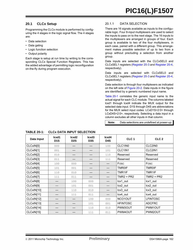
PIC16(L)F1507
20.1 CLCx Setup
Programming the CLCx module is performed by config-uring the 4 stages in the logic signal flow. The 4 stagesare:
• Data selection
• Data gating
• Logic function selection
• Output polarity
Each stage is setup at run time by writing to the corre-sponding CLCx Special Function Registers. This hasthe added advantage of permitting logic reconfigurationon-the-fly during program execution.
20.1.1 DATA SELECTION
There are 16 signals available as inputs to the configu-rable logic. Four 8-input multiplexers are used to selectthe inputs to pass on to the next stage. The 16 inputs tothe multiplexers are arranged in groups of four. Eachgroup is available to two of the four multiplexers, ineach case, paired with a different group. This arrange-ment makes possible selection of up to two from agroup without precluding a selection from anothergroup.
Data inputs are selected with the CLCxSEL0 andCLCxSEL1 registers (Register 20-3 and Register 20-4,respectively).
Data inputs are selected with CLCxSEL0 andCLCxSEL1 registers (Register 20-3 and Register 20-4,respectively).
Data selection is through four multiplexers as indicatedon the left side of Figure 20-2. Data inputs in the figureare identified by a generic numbered input name.
Table 20-1 correlates the generic input name to theactual signal for each CLC module. The columns labeledlcxd1 through lcxd4 indicate the MUX output for theselected data input. D1S through D4S are abbreviationsfor the MUX select input codes: LCxD1S<2:0> throughLCxD4S<2:0>, respectively. Selecting a data input in acolumn excludes all other inputs in that column.
Note: Data selections are undefined at power-up.
TABLE 20-1: CLCx DATA INPUT SELECTION
Data Inputlcxd1D1S
lcxd2D2S
lcxd3D3S
lcxd4D4S
CLC 1 CLC 2
CLCxIN[0] 000 — — 100 CLC1IN0 CLC2IN0
CLCxIN[1] 001 — — 101 CLC1IN1 CLC2IN1
CLCxIN[2] 010 — — 110 Reserved Reserved
CLCxIN[3] 011 — — 111 Reserved Reserved
CLCxIN[4] 100 000 — — FOSC FOSC
CLCxIN[5] 101 001 — — TMR0IF TMR0IF
CLCxIN[6] 110 010 — — TMR1IF TMR1IF
CLCxIN[7] 111 011 — — TMR2 = PR2 TMR2 = PR2
CLCxIN[8] — 100 000 — lcx1_out lcx1_out
CLCxIN[9] — 101 001 — lcx2_out lcx2_out
CLCxIN[10] — 110 010 — lcx3_out lcx3_out
CLCxIN[11] — 111 011 — lcx4_out lcx4_out
CLCxIN[12] — — 100 000 NCO1OUT LFINTOSC
CLCxIN[13] — — 101 001 HFINTOSC ADCFRC
CLCxIN[14] — — 110 010 PWM3OUT PWM1OUT
CLCxIN[15] — — 111 011 PWM4OUT PWM2OUT
2011 Microchip Technology Inc. Preliminary DS41586A-page 162
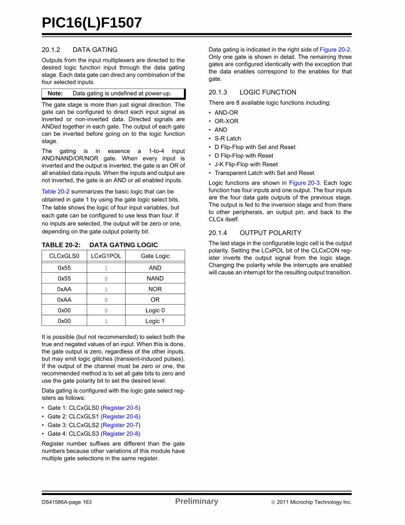
PIC16(L)F1507
20.1.2 DATA GATING
Outputs from the input multiplexers are directed to thedesired logic function input through the data gatingstage. Each data gate can direct any combination of thefour selected inputs.
The gate stage is more than just signal direction. Thegate can be configured to direct each input signal asinverted or non-inverted data. Directed signals areANDed together in each gate. The output of each gatecan be inverted before going on to the logic functionstage.
The gating is in essence a 1-to-4 inputAND/NAND/OR/NOR gate. When every input isinverted and the output is inverted, the gate is an OR ofall enabled data inputs. When the inputs and output arenot inverted, the gate is an AND or all enabled inputs.
Table 20-2 summarizes the basic logic that can be obtained in gate 1 by using the gate logic select bits. The table shows the logic of four input variables, but each gate can be configured to use less than four. If no inputs are selected, the output will be zero or one, depending on the gate output polarity bit.
It is possible (but not recommended) to select both thetrue and negated values of an input. When this is done,the gate output is zero, regardless of the other inputs,but may emit logic glitches (transient-induced pulses).If the output of the channel must be zero or one, therecommended method is to set all gate bits to zero anduse the gate polarity bit to set the desired level.
Data gating is configured with the logic gate select reg-isters as follows:
• Gate 1: CLCxGLS0 (Register 20-5)
• Gate 2: CLCxGLS1 (Register 20-6)
• Gate 3: CLCxGLS2 (Register 20-7)
• Gate 4: CLCxGLS3 (Register 20-8)
Register number suffixes are different than the gatenumbers because other variations of this module havemultiple gate selections in the same register.
Data gating is indicated in the right side of Figure 20-2.Only one gate is shown in detail. The remaining threegates are configured identically with the exception thatthe data enables correspond to the enables for thatgate.
20.1.3 LOGIC FUNCTION
There are 8 available logic functions including:
• AND-OR
• OR-XOR
• AND
• S-R Latch
• D Flip-Flop with Set and Reset
• D Flip-Flop with Reset
• J-K Flip-Flop with Reset
• Transparent Latch with Set and Reset
Logic functions are shown in Figure 20-3. Each logicfunction has four inputs and one output. The four inputsare the four data gate outputs of the previous stage.The output is fed to the inversion stage and from thereto other peripherals, an output pin, and back to theCLCx itself.
20.1.4 OUTPUT POLARITY
The last stage in the configurable logic cell is the outputpolarity. Setting the LCxPOL bit of the CLCxCON reg-ister inverts the output signal from the logic stage.Changing the polarity while the interrupts are enabledwill cause an interrupt for the resulting output transition.
Note: Data gating is undefined at power-up.
TABLE 20-2: DATA GATING LOGIC
CLCxGLS0 LCxG1POL Gate Logic
0x55 1 AND
0x55 0 NAND
0xAA 1 NOR
0xAA 0 OR
0x00 0 Logic 0
0x00 1 Logic 1
DS41586A-page 163 Preliminary 2011 Microchip Technology Inc.
PIC16(L)F1507
20.1.5 CLCx SETUP STEPS
The following steps should be followed when setting upthe CLCx:
• Disable CLCx by clearing the LCxEN bit.
• Select desired inputs using CLCxSEL0 and CLCxSEL1 registers (See Table 20-1).
• Clear any associated ANSEL bits.• Set all TRIS bits associated with inputs.
• Clear all TRIS bits associated with outputs.
• Enable the chosen inputs through the four gates using CLCxGLS0, CLCxGLS1, CLCxGLS2, and CLCxGLS3 registers.
• Select the gate output polarities with the LCx-POLy bits of the CLCxPOL register.
• Select the desired logic function with the LCxMODE<2:0> bits of the CLCxCON register.
• Select the desired polarity of the logic output with the LCxPOL bit of the CLCxPOL register. (This step may be combined with the previous gate out-put polarity step).
• If driving the CLCx pin, set the LCxOE bit of the CLCxCON register and also clear the TRIS bit corresponding to that output.
• If interrupts are desired, configure the following bits:
- Set the LCxINTP bit in the CLCxCON register for rising event.
- Set the LCxINTN bit in the CLCxCON register or falling event.
- Set the CLCxIE bit of the associated PIE registers.
- Set the GIE and PEIE bits of the INTCON register.
• Enable the CLCx by setting the LCxEN bit of the CLCxCON register.
20.2 CLCx Interrupts
An interrupt will be generated upon a change in theoutput value of the CLCx when the appropriate interruptenables are set. A rising edge detector and a fallingedge detector are present in each CLC for this purpose.
The LCxIF bit of the associated PIR registers will be setwhen either edge detector is triggered and its associ-ated enable bit is set. The LCxINTP enables risingedge interrupts and the LCxINTN bit enables fallingedge interrupts. Both are located in the CLCxCON reg-ister.
To fully enable the interrupt, set the following bits:
• LCxON bit of the CLCxCON register
• LCxIE bit of the associated PIE registers
• LCxINTP bit of the CLCxCON register (for a rising edge detection)
• LCxINTN bit of the CLCxCON register (for a fall-ing edge detection)
• PEIE and GIE bits of the INTCON register
The LCxIF bit of the associated PIR registers, must becleared in software as part of the interrupt service. Ifanother edge is detected while this flag is beingcleared, the flag will still be set at the end of thesequence.
20.3 Output Mirror Copies
Mirror copies of all LCxCON output bits are containedin the CLCxDATA register. Reading this register readsthe outputs of all CLCs simultaneously. This preventsany reading skew introduced by testing or reading theCLCxOUT bits in the individual CLCxCON registers.
20.4 Effects of a Reset
The CLCxCON register is cleared to zero as the resultof a Reset. All other selection and gating values remainunchanged.
20.5 Operation During Sleep
The CLC module operates independently from the system clock and will continue to run during Sleep, provided that the input sources selected remain active.
The HFINTOSC remains active during Sleep when the CLC module is enabled and the HFINTOSC is selected as an input source, regardless of the system clock source selected.
In other words, if the HFINTOSC is simultaneously selected as the system clock and as a CLC input source, when the CLC is enabled, the CPU will go idle during Sleep, but the CLC will continue to operate and the HFINTOSC will remain active.
This will have a direct effect on the Sleep mode current.
2011 Microchip Technology Inc. Preliminary DS41586A-page 164
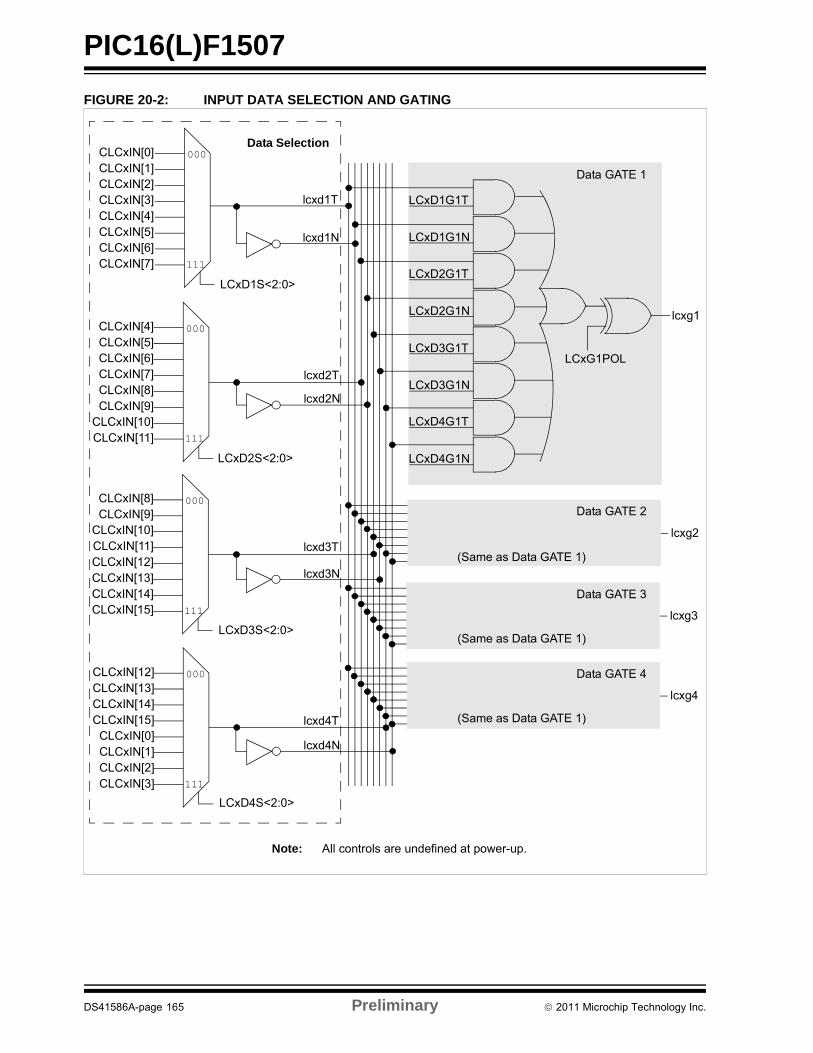
PIC16(L)F1507
FIGURE 20-2: INPUT DATA SELECTION AND GATING
lcxg1
LCxG1POL
Data GATE 1
LCxD1G1T
lcxg2
lcxg3
lcxg4
Data GATE 2
Data GATE 3
Data GATE 4
LCxD1G1N
LCxD2G1T
LCxD2G1N
LCxD3G1T
LCxD3G1N
LCxD4G1T
LCxD4G1N
LCxD1S<2:0>
LCxD2S<2:0>
LCxD3S<2:0>
LCxD4S<2:0>
CLCxIN[0]CLCxIN[1]CLCxIN[2]CLCxIN[3]CLCxIN[4]CLCxIN[5]CLCxIN[6]CLCxIN[7]
000
111
000
111
000
111
000
111
CLCxIN[4]CLCxIN[5]CLCxIN[6]CLCxIN[7]CLCxIN[8]CLCxIN[9]
CLCxIN[10]CLCxIN[11]
CLCxIN[8]CLCxIN[9]
CLCxIN[10]CLCxIN[11]CLCxIN[12]CLCxIN[13]CLCxIN[14]CLCxIN[15]
CLCxIN[12]CLCxIN[13]CLCxIN[14]CLCxIN[15]
CLCxIN[0]CLCxIN[1]CLCxIN[2]CLCxIN[3]
Data Selection
Note: All controls are undefined at power-up.
lcxd1T
lcxd1N
lcxd2T
lcxd2N
lcxd3T
lcxd3N
lcxd4T
lcxd4N
(Same as Data GATE 1)
(Same as Data GATE 1)
(Same as Data GATE 1)
DS41586A-page 165 Preliminary 2011 Microchip Technology Inc.
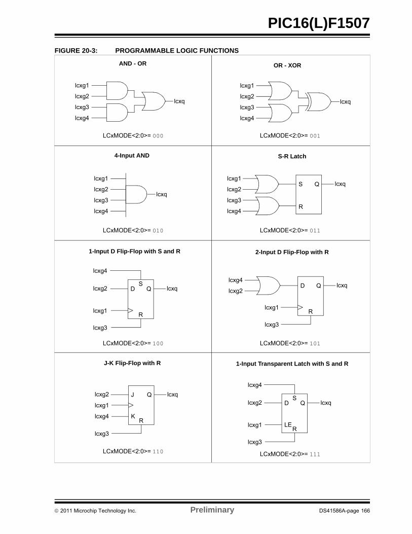
PIC16(L)F1507
FIGURE 20-3: PROGRAMMABLE LOGIC FUNCTIONS
lcxg1
lcxg2
lcxg3
lcxg4
lcxq
lcxg1
lcxg2
lcxg3
lcxg4
lcxq
lcxg1
lcxg2
lcxg3
lcxg4
lcxq
S
R
Qlcxg1
lcxg2
lcxg3
lcxg4
lcxq
D Q
lcxg1
lcxg2
lcxg3
lcxg4
lcxqS
R
J Qlcxg2
lcxg3
lcxg4
lcxq
R
lcxg1
K
D Q
lcxg1
lcxg2
lcxg3
lcxg4
lcxqS
R
D Q
lcxg1
lcxg3
lcxq
R
lcxg4
lcxg2
LCxMODE<2:0>= 000
LCxMODE<2:0>= 010
LCxMODE<2:0>= 001
LCxMODE<2:0>= 011
LCxMODE<2:0>= 100
LCxMODE<2:0>= 110
LCxMODE<2:0>= 101
LCxMODE<2:0>= 111
LE
AND - OR OR - XOR
4-Input AND S-R Latch
1-Input D Flip-Flop with S and R 2-Input D Flip-Flop with R
1-Input Transparent Latch with S and RJ-K Flip-Flop with R
2011 Microchip Technology Inc. Preliminary DS41586A-page 166
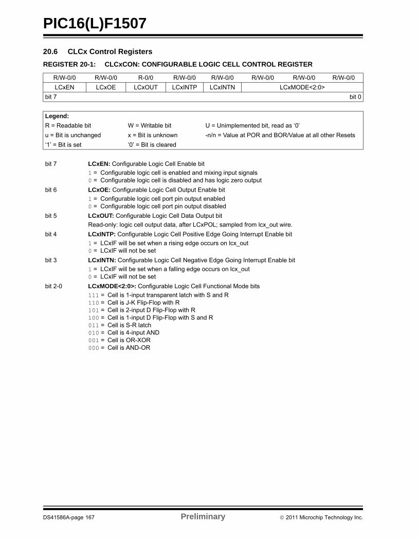
PIC16(L)F1507
20.6 CLCx Control Registers
REGISTER 20-1: CLCxCON: CONFIGURABLE LOGIC CELL CONTROL REGISTER
R/W-0/0 R/W-0/0 R-0/0 R/W-0/0 R/W-0/0 R/W-0/0 R/W-0/0 R/W-0/0
LCxEN LCxOE LCxOUT LCxINTP LCxINTN LCxMODE<2:0>
bit 7 bit 0
Legend:
R = Readable bit W = Writable bit U = Unimplemented bit, read as ‘0’
u = Bit is unchanged x = Bit is unknown -n/n = Value at POR and BOR/Value at all other Resets
‘1’ = Bit is set ‘0’ = Bit is cleared
bit 7 LCxEN: Configurable Logic Cell Enable bit
1 = Configurable logic cell is enabled and mixing input signals0 = Configurable logic cell is disabled and has logic zero output
bit 6 LCxOE: Configurable Logic Cell Output Enable bit
1 = Configurable logic cell port pin output enabled0 = Configurable logic cell port pin output disabled
bit 5 LCxOUT: Configurable Logic Cell Data Output bit
Read-only: logic cell output data, after LCxPOL; sampled from lcx_out wire.
bit 4 LCxINTP: Configurable Logic Cell Positive Edge Going Interrupt Enable bit
1 = LCxIF will be set when a rising edge occurs on lcx_out0 = LCxIF will not be set
bit 3 LCxINTN: Configurable Logic Cell Negative Edge Going Interrupt Enable bit
1 = LCxIF will be set when a falling edge occurs on lcx_out0 = LCxIF will not be set
bit 2-0 LCxMODE<2:0>: Configurable Logic Cell Functional Mode bits
111 = Cell is 1-input transparent latch with S and R110 = Cell is J-K Flip-Flop with R101 = Cell is 2-input D Flip-Flop with R100 = Cell is 1-input D Flip-Flop with S and R011 = Cell is S-R latch010 = Cell is 4-input AND001 = Cell is OR-XOR000 = Cell is AND-OR
DS41586A-page 167 Preliminary 2011 Microchip Technology Inc.
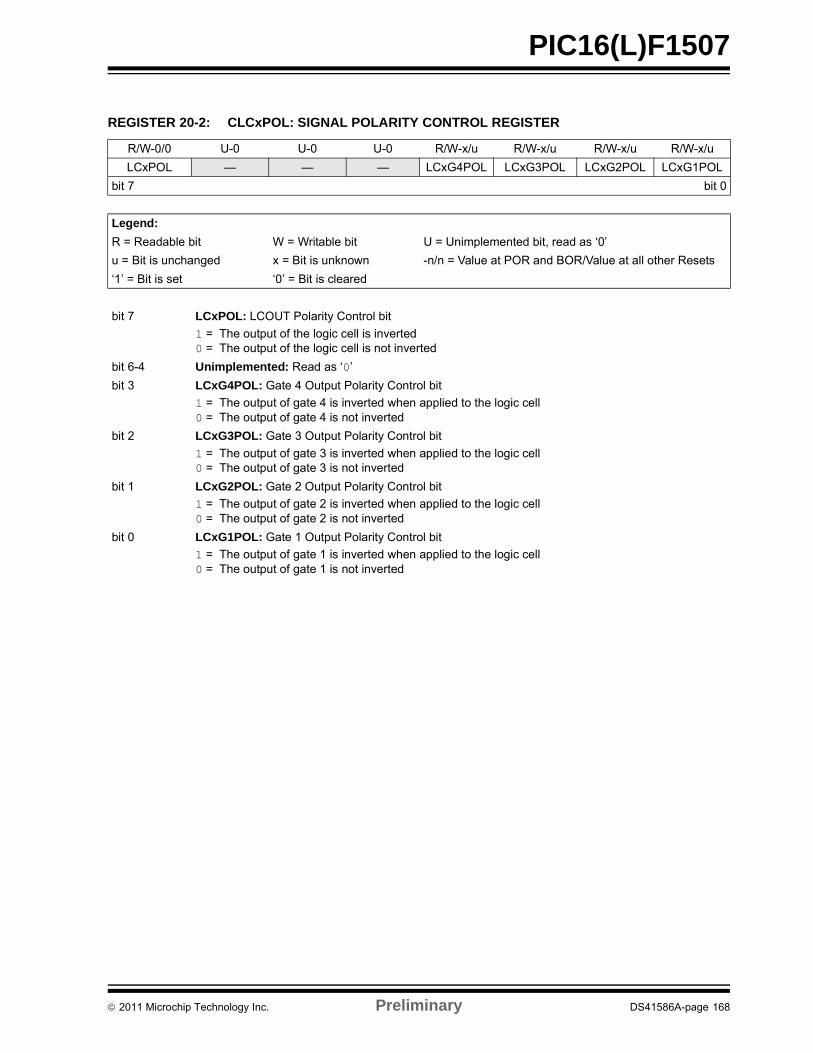
PIC16(L)F1507
REGISTER 20-2: CLCxPOL: SIGNAL POLARITY CONTROL REGISTER
R/W-0/0 U-0 U-0 U-0 R/W-x/u R/W-x/u R/W-x/u R/W-x/u
LCxPOL — — — LCxG4POL LCxG3POL LCxG2POL LCxG1POL
bit 7 bit 0
Legend:
R = Readable bit W = Writable bit U = Unimplemented bit, read as ‘0’
u = Bit is unchanged x = Bit is unknown -n/n = Value at POR and BOR/Value at all other Resets
‘1’ = Bit is set ‘0’ = Bit is cleared
bit 7 LCxPOL: LCOUT Polarity Control bit
1 = The output of the logic cell is inverted0 = The output of the logic cell is not inverted
bit 6-4 Unimplemented: Read as ‘0’
bit 3 LCxG4POL: Gate 4 Output Polarity Control bit
1 = The output of gate 4 is inverted when applied to the logic cell0 = The output of gate 4 is not inverted
bit 2 LCxG3POL: Gate 3 Output Polarity Control bit
1 = The output of gate 3 is inverted when applied to the logic cell0 = The output of gate 3 is not inverted
bit 1 LCxG2POL: Gate 2 Output Polarity Control bit
1 = The output of gate 2 is inverted when applied to the logic cell0 = The output of gate 2 is not inverted
bit 0 LCxG1POL: Gate 1 Output Polarity Control bit
1 = The output of gate 1 is inverted when applied to the logic cell0 = The output of gate 1 is not inverted
2011 Microchip Technology Inc. Preliminary DS41586A-page 168
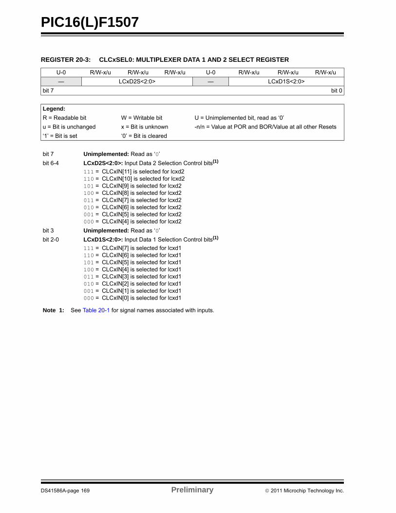
PIC16(L)F1507
REGISTER 20-3: CLCxSEL0: MULTIPLEXER DATA 1 AND 2 SELECT REGISTER
U-0 R/W-x/u R/W-x/u R/W-x/u U-0 R/W-x/u R/W-x/u R/W-x/u
— LCxD2S<2:0> — LCxD1S<2:0>
bit 7 bit 0
Legend:
R = Readable bit W = Writable bit U = Unimplemented bit, read as ‘0’
u = Bit is unchanged x = Bit is unknown -n/n = Value at POR and BOR/Value at all other Resets
‘1’ = Bit is set ‘0’ = Bit is cleared
bit 7 Unimplemented: Read as ‘0’
bit 6-4 LCxD2S<2:0>: Input Data 2 Selection Control bits(1)
111 = CLCxIN[11] is selected for lcxd2110 = CLCxIN[10] is selected for lcxd2101 = CLCxIN[9] is selected for lcxd2100 = CLCxIN[8] is selected for lcxd2011 = CLCxIN[7] is selected for lcxd2010 = CLCxIN[6] is selected for lcxd2001 = CLCxIN[5] is selected for lcxd2000 = CLCxIN[4] is selected for lcxd2
bit 3 Unimplemented: Read as ‘0’
bit 2-0 LCxD1S<2:0>: Input Data 1 Selection Control bits(1)
111 = CLCxIN[7] is selected for lcxd1110 = CLCxIN[6] is selected for lcxd1101 = CLCxIN[5] is selected for lcxd1100 = CLCxIN[4] is selected for lcxd1011 = CLCxIN[3] is selected for lcxd1010 = CLCxIN[2] is selected for lcxd1001 = CLCxIN[1] is selected for lcxd1000 = CLCxIN[0] is selected for lcxd1
Note 1: See Table 20-1 for signal names associated with inputs.
DS41586A-page 169 Preliminary 2011 Microchip Technology Inc.
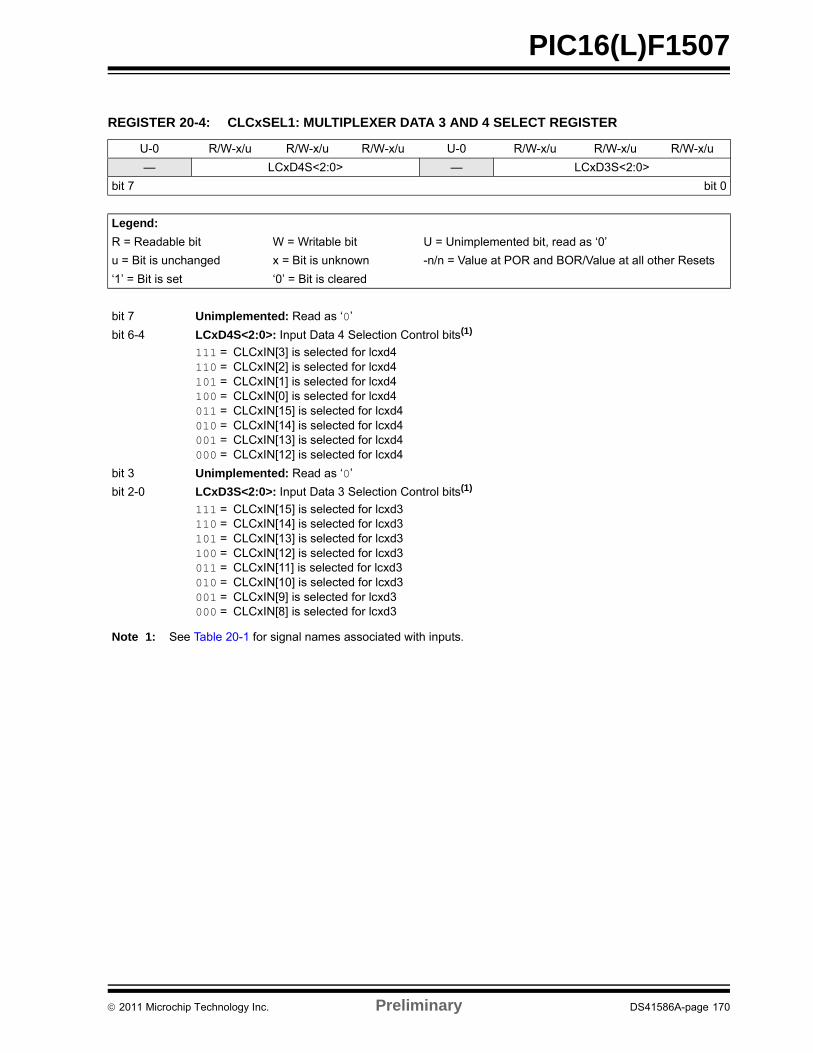
PIC16(L)F1507
REGISTER 20-4: CLCxSEL1: MULTIPLEXER DATA 3 AND 4 SELECT REGISTER
U-0 R/W-x/u R/W-x/u R/W-x/u U-0 R/W-x/u R/W-x/u R/W-x/u
— LCxD4S<2:0> — LCxD3S<2:0>
bit 7 bit 0
Legend:
R = Readable bit W = Writable bit U = Unimplemented bit, read as ‘0’
u = Bit is unchanged x = Bit is unknown -n/n = Value at POR and BOR/Value at all other Resets
‘1’ = Bit is set ‘0’ = Bit is cleared
bit 7 Unimplemented: Read as ‘0’
bit 6-4 LCxD4S<2:0>: Input Data 4 Selection Control bits(1)
111 = CLCxIN[3] is selected for lcxd4110 = CLCxIN[2] is selected for lcxd4101 = CLCxIN[1] is selected for lcxd4100 = CLCxIN[0] is selected for lcxd4011 = CLCxIN[15] is selected for lcxd4010 = CLCxIN[14] is selected for lcxd4001 = CLCxIN[13] is selected for lcxd4000 = CLCxIN[12] is selected for lcxd4
bit 3 Unimplemented: Read as ‘0’
bit 2-0 LCxD3S<2:0>: Input Data 3 Selection Control bits(1)
111 = CLCxIN[15] is selected for lcxd3110 = CLCxIN[14] is selected for lcxd3101 = CLCxIN[13] is selected for lcxd3100 = CLCxIN[12] is selected for lcxd3011 = CLCxIN[11] is selected for lcxd3010 = CLCxIN[10] is selected for lcxd3001 = CLCxIN[9] is selected for lcxd3000 = CLCxIN[8] is selected for lcxd3
Note 1: See Table 20-1 for signal names associated with inputs.
2011 Microchip Technology Inc. Preliminary DS41586A-page 170
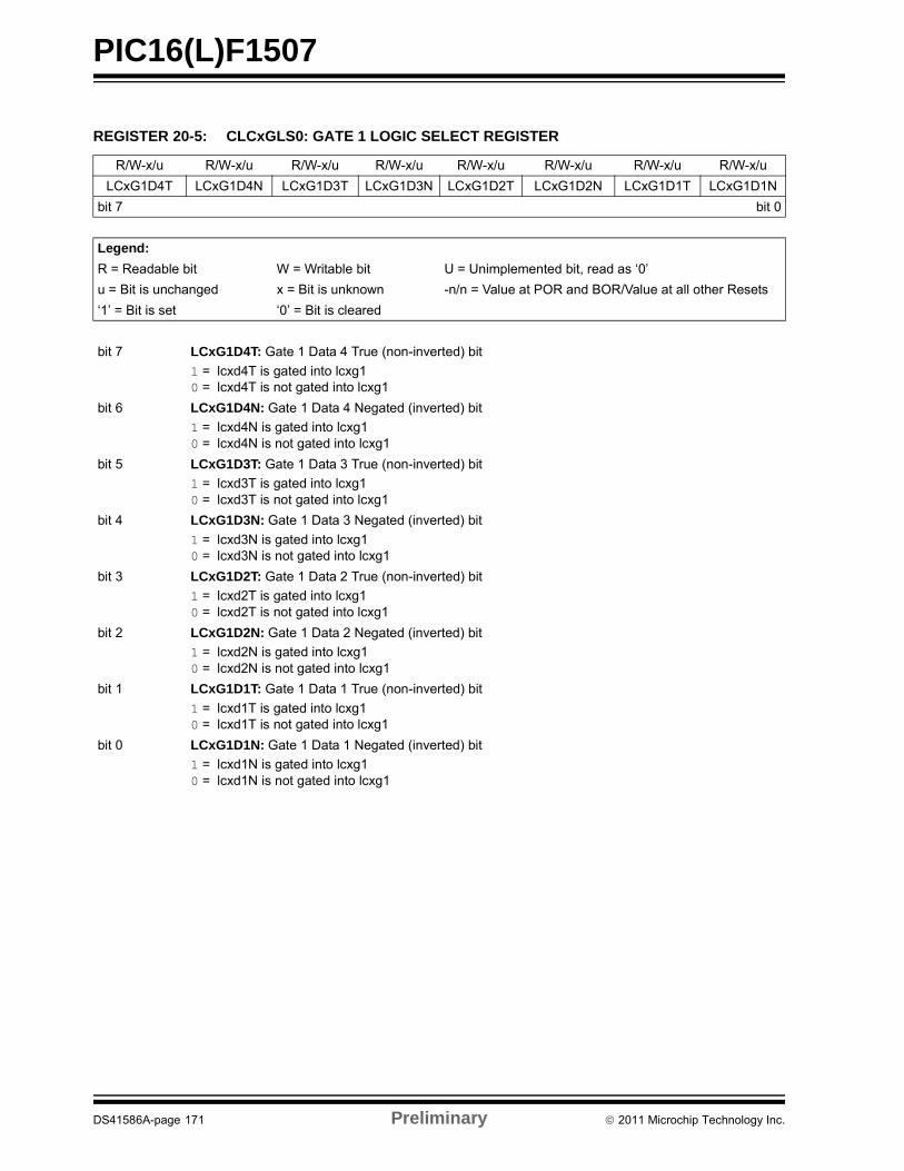
PIC16(L)F1507
REGISTER 20-5: CLCxGLS0: GATE 1 LOGIC SELECT REGISTER
R/W-x/u R/W-x/u R/W-x/u R/W-x/u R/W-x/u R/W-x/u R/W-x/u R/W-x/u
LCxG1D4T LCxG1D4N LCxG1D3T LCxG1D3N LCxG1D2T LCxG1D2N LCxG1D1T LCxG1D1N
bit 7 bit 0
Legend:
R = Readable bit W = Writable bit U = Unimplemented bit, read as ‘0’
u = Bit is unchanged x = Bit is unknown -n/n = Value at POR and BOR/Value at all other Resets
‘1’ = Bit is set ‘0’ = Bit is cleared
bit 7 LCxG1D4T: Gate 1 Data 4 True (non-inverted) bit
1 = lcxd4T is gated into lcxg10 = lcxd4T is not gated into lcxg1
bit 6 LCxG1D4N: Gate 1 Data 4 Negated (inverted) bit
1 = lcxd4N is gated into lcxg10 = lcxd4N is not gated into lcxg1
bit 5 LCxG1D3T: Gate 1 Data 3 True (non-inverted) bit
1 = lcxd3T is gated into lcxg10 = lcxd3T is not gated into lcxg1
bit 4 LCxG1D3N: Gate 1 Data 3 Negated (inverted) bit
1 = lcxd3N is gated into lcxg10 = lcxd3N is not gated into lcxg1
bit 3 LCxG1D2T: Gate 1 Data 2 True (non-inverted) bit
1 = lcxd2T is gated into lcxg10 = lcxd2T is not gated into lcxg1
bit 2 LCxG1D2N: Gate 1 Data 2 Negated (inverted) bit
1 = lcxd2N is gated into lcxg10 = lcxd2N is not gated into lcxg1
bit 1 LCxG1D1T: Gate 1 Data 1 True (non-inverted) bit
1 = lcxd1T is gated into lcxg10 = lcxd1T is not gated into lcxg1
bit 0 LCxG1D1N: Gate 1 Data 1 Negated (inverted) bit
1 = lcxd1N is gated into lcxg10 = lcxd1N is not gated into lcxg1
DS41586A-page 171 Preliminary 2011 Microchip Technology Inc.
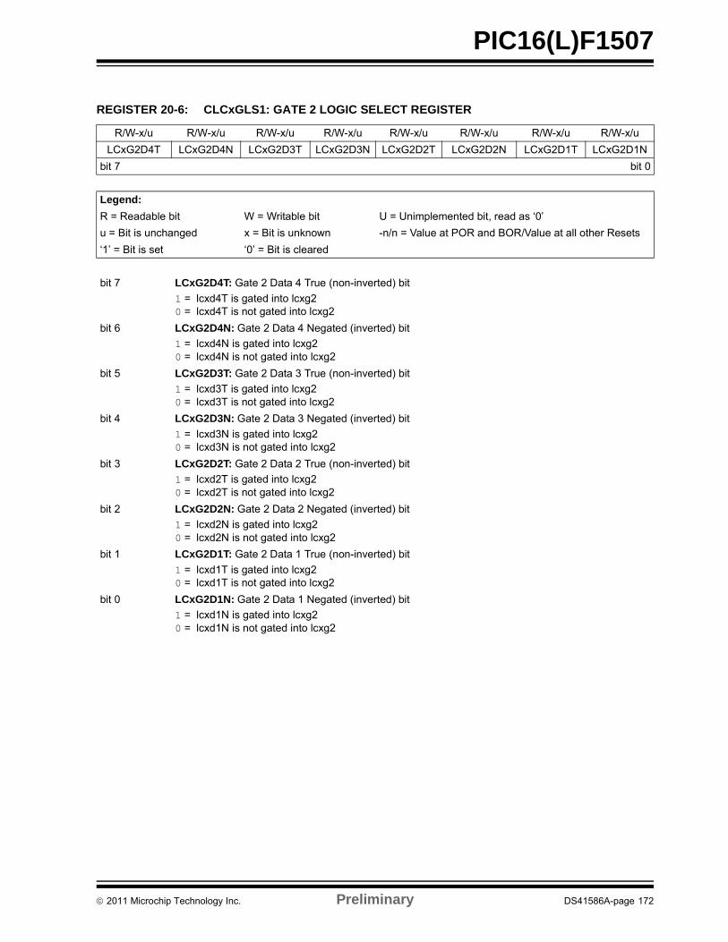
PIC16(L)F1507
REGISTER 20-6: CLCxGLS1: GATE 2 LOGIC SELECT REGISTER
R/W-x/u R/W-x/u R/W-x/u R/W-x/u R/W-x/u R/W-x/u R/W-x/u R/W-x/u
LCxG2D4T LCxG2D4N LCxG2D3T LCxG2D3N LCxG2D2T LCxG2D2N LCxG2D1T LCxG2D1N
bit 7 bit 0
Legend:
R = Readable bit W = Writable bit U = Unimplemented bit, read as ‘0’
u = Bit is unchanged x = Bit is unknown -n/n = Value at POR and BOR/Value at all other Resets
‘1’ = Bit is set ‘0’ = Bit is cleared
bit 7 LCxG2D4T: Gate 2 Data 4 True (non-inverted) bit
1 = lcxd4T is gated into lcxg20 = lcxd4T is not gated into lcxg2
bit 6 LCxG2D4N: Gate 2 Data 4 Negated (inverted) bit
1 = lcxd4N is gated into lcxg20 = lcxd4N is not gated into lcxg2
bit 5 LCxG2D3T: Gate 2 Data 3 True (non-inverted) bit
1 = lcxd3T is gated into lcxg20 = lcxd3T is not gated into lcxg2
bit 4 LCxG2D3N: Gate 2 Data 3 Negated (inverted) bit
1 = lcxd3N is gated into lcxg20 = lcxd3N is not gated into lcxg2
bit 3 LCxG2D2T: Gate 2 Data 2 True (non-inverted) bit
1 = lcxd2T is gated into lcxg20 = lcxd2T is not gated into lcxg2
bit 2 LCxG2D2N: Gate 2 Data 2 Negated (inverted) bit
1 = lcxd2N is gated into lcxg20 = lcxd2N is not gated into lcxg2
bit 1 LCxG2D1T: Gate 2 Data 1 True (non-inverted) bit
1 = lcxd1T is gated into lcxg20 = lcxd1T is not gated into lcxg2
bit 0 LCxG2D1N: Gate 2 Data 1 Negated (inverted) bit
1 = lcxd1N is gated into lcxg20 = lcxd1N is not gated into lcxg2
2011 Microchip Technology Inc. Preliminary DS41586A-page 172
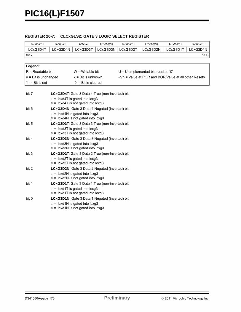
PIC16(L)F1507
REGISTER 20-7: CLCxGLS2: GATE 3 LOGIC SELECT REGISTER
R/W-x/u R/W-x/u R/W-x/u R/W-x/u R/W-x/u R/W-x/u R/W-x/u R/W-x/u
LCxG3D4T LCxG3D4N LCxG3D3T LCxG3D3N LCxG3D2T LCxG3D2N LCxG3D1T LCxG3D1N
bit 7 bit 0
Legend:
R = Readable bit W = Writable bit U = Unimplemented bit, read as ‘0’
u = Bit is unchanged x = Bit is unknown -n/n = Value at POR and BOR/Value at all other Resets
‘1’ = Bit is set ‘0’ = Bit is cleared
bit 7 LCxG3D4T: Gate 3 Data 4 True (non-inverted) bit
1 = lcxd4T is gated into lcxg30 = lcxd4T is not gated into lcxg3
bit 6 LCxG3D4N: Gate 3 Data 4 Negated (inverted) bit
1 = lcxd4N is gated into lcxg30 = lcxd4N is not gated into lcxg3
bit 5 LCxG3D3T: Gate 3 Data 3 True (non-inverted) bit
1 = lcxd3T is gated into lcxg30 = lcxd3T is not gated into lcxg3
bit 4 LCxG3D3N: Gate 3 Data 3 Negated (inverted) bit
1 = lcxd3N is gated into lcxg30 = lcxd3N is not gated into lcxg3
bit 3 LCxG3D2T: Gate 3 Data 2 True (non-inverted) bit
1 = lcxd2T is gated into lcxg30 = lcxd2T is not gated into lcxg3
bit 2 LCxG3D2N: Gate 3 Data 2 Negated (inverted) bit
1 = lcxd2N is gated into lcxg30 = lcxd2N is not gated into lcxg3
bit 1 LCxG3D1T: Gate 3 Data 1 True (non-inverted) bit
1 = lcxd1T is gated into lcxg30 = lcxd1T is not gated into lcxg3
bit 0 LCxG3D1N: Gate 3 Data 1 Negated (inverted) bit
1 = lcxd1N is gated into lcxg30 = lcxd1N is not gated into lcxg3
DS41586A-page 173 Preliminary 2011 Microchip Technology Inc.

PIC16(L)F1507
REGISTER 20-8: CLCxGLS3: GATE 4 LOGIC SELECT REGISTER
R/W-x/u R/W-x/u R/W-x/u R/W-x/u R/W-x/u R/W-x/u R/W-x/u R/W-x/u
LCxG4D4T LCxG4D4N LCxG4D3T LCxG4D3N LCxG4D2T LCxG4D2N LCxG4D1T LCxG4D1N
bit 7 bit 0
Legend:
R = Readable bit W = Writable bit U = Unimplemented bit, read as ‘0’
u = Bit is unchanged x = Bit is unknown -n/n = Value at POR and BOR/Value at all other Resets
‘1’ = Bit is set ‘0’ = Bit is cleared
bit 7 LCxG4D4T: Gate 4 Data 4 True (non-inverted) bit
1 = lcxd4T is gated into lcxg40 = lcxd4T is not gated into lcxg4
bit 6 LCxG4D4N: Gate 4 Data 4 Negated (inverted) bit
1 = lcxd4N is gated into lcxg40 = lcxd4N is not gated into lcxg4
bit 5 LCxG4D3T: Gate 4 Data 3 True (non-inverted) bit
1 = lcxd3T is gated into lcxg40 = lcxd3T is not gated into lcxg4
bit 4 LCxG4D3N: Gate 4 Data 3 Negated (inverted) bit
1 = lcxd3N is gated into lcxg40 = lcxd3N is not gated into lcxg4
bit 3 LCxG4D2T: Gate 4 Data 2 True (non-inverted) bit
1 = lcxd2T is gated into lcxg40 = lcxd2T is not gated into lcxg4
bit 2 LCxG4D2N: Gate 4 Data 2 Negated (inverted) bit
1 = lcxd2N is gated into lcxg40 = lcxd2N is not gated into lcxg4
bit 1 LCxG4D1T: Gate 4 Data 1 True (non-inverted) bit
1 = lcxd1T is gated into lcxg40 = lcxd1T is not gated into lcxg4
bit 0 LCxG4D1N: Gate 4 Data 1 Negated (inverted) bit
1 = lcxd1N is gated into lcxg40 = lcxd1N is not gated into lcxg4
2011 Microchip Technology Inc. Preliminary DS41586A-page 174
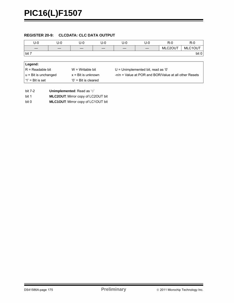
PIC16(L)F1507
REGISTER 20-9: CLCDATA: CLC DATA OUTPUT
U-0 U-0 U-0 U-0 U-0 U-0 R-0 R-0
— — — — — — MLC2OUT MLC1OUT
bit 7 bit 0
Legend:
R = Readable bit W = Writable bit U = Unimplemented bit, read as ‘0’
u = Bit is unchanged x = Bit is unknown -n/n = Value at POR and BOR/Value at all other Resets
‘1’ = Bit is set ‘0’ = Bit is cleared
bit 7-2 Unimplemented: Read as ‘0’
bit 1 MLC2OUT: Mirror copy of LC2OUT bit
bit 0 MLC1OUT: Mirror copy of LC1OUT bit
DS41586A-page 175 Preliminary 2011 Microchip Technology Inc.
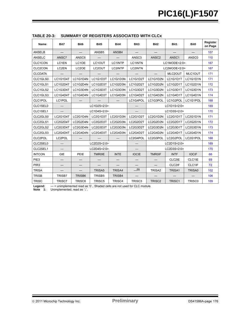
PIC16(L)F1507
TABLE 20-3: SUMMARY OF REGISTERS ASSOCIATED WITH CLCx
Name Bit7 Bit6 Bit5 Bit4 BIt3 Bit2 Bit1 Bit0Register on Page
ANSELB — — ANSB5 ANSB4 — — — — 107
ANSELC ANSC7 ANSC6 — — ANSC3 ANSC2 ANSC1 ANSC0 110
CLC1CON LC1EN LC1OE LC1OUT LC1INTP LC1INTN LC1MODE<2:0> 167
CLC2CON LC2EN LC2OE LC2OUT LC2INTP LC2INTN LC2MODE<2:0> 167
CLCDATA — — — — — — MLC2OUT MLC1OUT 171
CLC1GLS0 LC1G1D4T LC1G1D4N LC1G1D3T LC1G1D3N LC1G1D2T LC1G1D2N LC1G1D1T LC1G1D1N 171
CLC1GLS1 LC1G2D4T LC1G2D4N LC1G2D3T LC1G2D3N LC1G2D2T LC1G2D2N LC1G2D1T LC1G2D1N 172
CLC1GLS2 LC1G3D4T LC1G3D4N LC1G3D3T LC1G3D3N LC1G3D2T LC1G3D2N LC1G3D1T LC1G3D1N 173
CLC1GLS3 LC1G4D4T LC1G4D4N LC1G4D3T LC1G4D3N LC1G4D2T LC1G4D2N LC1G4D1T LC1G4D1N 174
CLC1POL LC1POL — — — LC1G4POL LC1G3POL LC1G2POL LC1G1POL 168
CLC1SEL0 — LC1D2S<2:0> — LC1D1S<2:0> 169
CLC1SEL1 — LC1D4S<2:0> — LC1D3S<2:0> 170
CLC2GLS0 LC2G1D4T LC2G1D4N LC2G1D3T LC2G1D3N LC2G1D2T LC2G1D2N LC2G1D1T LC2G1D1N 171
CLC2GLS1 LC2G2D4T LC2G2D4N LC2G2D3T LC2G2D3N LC2G2D2T LC2G2D2N LC2G2D1T LC2G2D1N 172
CLC2GLS2 LC2G3D4T LC2G3D4N LC2G3D3T LC2G3D3N LC2G3D2T LC2G3D2N LC2G3D1T LC2G3D1N 173
CLC2GLS3 LC2G4D4T LC2G4D4N LC2G4D3T LC2G4D3N LC2G4D2T LC2G4D2N LC2G4D1T LC2G4D1N 174
CLC2POL LC2POL — — — LC2G4POL LC2G3POL LC2G2POL LC2G1POL 168
CLC2SEL0 — LC2D2S<2:0> — LC2D1S<2:0> 169
CLC2SEL1 — LC2D4S<2:0> — LC2D3S<2:0> 170
INTCON GIE PEIE TMR0IE INTE IOCIE TMR0IF INTF IOCIF 66
PIE3 — — — — — — CLC2IE CLC1IE 69
PIR3 — — — — — — CLC2IF CLC1IF 72
TRISA — — TRISA5 TRISA4 —(1) TRISA2 TRISA1 TRISA0 102
TRISB TRISB7 TRISB6 TRISB5 TRISB4 — — — — 106
TRISC TRISC7 TRISC6 TRISC5 TRISC4 TRISC3 TRISC2 TRISC1 TRISC0 109
Legend: — = unimplemented read as ‘0’,. Shaded cells are not used for CLC module.Note 1: Unimplemented, read as ‘1’.
2011 Microchip Technology Inc. Preliminary DS41586A-page 176
PIC16(L)F1507
21.0 NUMERICALLY CONTROLLED OSCILLATOR (NCO) MODULE
The Numerically Controlled Oscillator (NCOx) moduleis a timer that uses the overflow from the addition of anincrement value to divide the input frequency. Theadvantage of the addition method over simple counterdriven timer is that the resolution of division does notvary with the divider value. The NCOx is most useful forapplications that require frequency accuracy and fineresolution at a fixed duty cycle.
Features of the NCOx include:
• 16-bit increment function• Fixed Duty Cycle (FDC) mode• Pulse Frequency (PF) mode• Output pulse width control• Multiple clock input sources• Output polarity control• Interrupt capability
Figure 21-1 is a simplified block diagram of the NCOxmodule.
DS41586A-page 177 Preliminary 2011 Microchip Technology Inc.
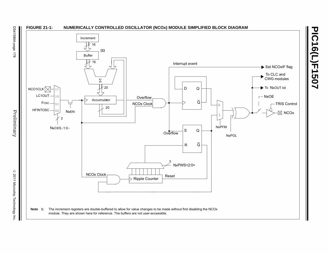
PIC
16(L)F
1507
DS
41
58
6A
-pa
ge
17
8P
relimin
ary
20
11
Micro
chip
Te
chn
olo
gy In
c.
DIAGRAM
To NxOUT bit
Set NCOxIF flag
NxPOL
To CLC andCWG modules
NCOx
NxOE
TRIS Control
FIGURE 21-1: NUMERICALLY CONTROLLED OSCILLATOR (NCOx) MODULE SIMPLIFIED BLOCK
NxEN
LC1OUT
HFINTOSC
NCO1CLK
2
NxCKS<1:0>
Note 1: The increment registers are double-buffered to allow for value changes to be made without first disabling the NCOx module. They are shown here for reference. The buffers are not user-accessible.
(1)
FOSC
10
00
01
11
Increment
Buffer
Accumulator
Overflow
NCOx Clock
D Q
Q
S Q
Q
Overflow
R
16
20
20
Interrupt event
NCOx Clock
0
1
NxPFM
Ripple CounterReset
NxPWS<2:0>3
16
PIC16(L)F1507
21.1 NCOx OPERATION
The NCOx operates by repeatedly adding a fixed valueto an accumulator. Additions occur at the input clockrate. The accumulator will overflow with a carryperiodically, which is the raw NCOx output. Thiseffectively reduces the input clock by the ratio of theaddition value to the maximum accumulator value. SeeEquation 21-1.
The NCOx output can be further modified by stretchingthe pulse or toggling a flip-flop. The modified NCOxoutput is then distributed internally to other peripheralsand optionally output to a pin. The accumulator overflowalso generates an interrupt.
The NCOx period changes in discrete steps to create anaverage frequency. This output depends on the ability ofthe receiving circuit (i.e., CWG or external resonantconverter circuitry) to average the NCOx output toreduce uncertainty.
21.1.1 NCOx CLOCK SOURCES
Clock sources available to the NCOx include:
• HFINTOSC• FOSC
• LCxOUT• CLKIN pin
The NCOx clock source is selected by configuring theNxCKS<2:0> bits in the NCOxCLK register.
21.1.2 ACCUMULATOR
The accumulator is a 20-bit register. Read and writeaccess to the Accumulator is available through threeregisters:
• NCOxACCL
• NCOxACCH
• NCOxACCU
21.1.3 ADDER
The NCOx Adder is a full adder, which operatesindependently from the system clock. The addition ofthe previous result and the increment value replacesthe accumulator value on the rising edge of each inputclock.
21.1.4 INCREMENT REGISTERS
The Increment value is stored in two 8-bit registersmaking up a 16-bit increment. In order of LSB to MSBthey are:
• NCOxINCL
• NCOxINCH
Both of the registers are readable and writeable. TheIncrement registers are double-buffered to allow forvalue changes to be made without first disabling theNCOx module.
The buffer loads are immediate when the module is dis-abled. Writing to the NCOxINCH register first is neces-sary because then the buffer is loaded synchronouslywith the NCOx operation after the write is executed onthe NCOxINCL register.
EQUATION 21-1:
Note: The increment buffer registers are notuser-accessible.
FOVERFLOWNCO Clock Frequency Increment Value
2n----------------------------------------------------------------------------------------------------------------=
n = Accumulator width in bits
DS41586A-page 179 Preliminary 2011 Microchip Technology Inc.
PIC16(L)F1507
21.2 FIXED DUTY CYCLE (FDC) MODE
In Fixed Duty Cycle (FDC) mode, every time theaccumulator overflows, the output is toggled. Thisprovides a 50% duty cycle, provided that the incrementvalue remains constant. For more information, seeFigure 21-2.
The FDC mode is selected by clearing the NxPFM bitin the NCOxCON register.
21.3 PULSE FREQUENCY (PF) MODE
In Pulse Frequency (PF) mode, every time the accumu-lator overflows, the output becomes active for one ormore clock periods. Once the clock period expires, theoutput returns to an inactive state. This provides apulsed output.
The output becomes active on the rising clock edgeimmediately following the overflow event. For moreinformation, see Figure 21-2.
The value of the active and inactive states depends onthe polarity bit, NxPOL in the NCOxCON register.
The PF mode is selected by setting the NxPFM bit inthe NCOxCON register.
21.3.1 OUTPUT PULSE WIDTH CONTROL
When operating in PF mode, the active state of the out-put can vary in width by multiple clock periods. Variouspulse widths are selected with the NxPWS<2:0> bits inthe NCOxCLK register.
When the selected pulse width is greater than theaccumulator overflow time frame, the output of theNCOx operation is indeterminate.
21.4 OUTPUT POLARITY CONTROL
The last stage in the NCOx module is the output polar-ity. The NxPOL bit in the NCOxCON register selects theoutput polarity. Changing the polarity while the inter-rupts are enabled will cause an interrupt for the result-ing output transition.
The NCOx output can be used internally by sourcecode or other peripherals. Accomplish this by readingthe NxOUT (read-only) bit of the NCOxCON register.
2011 Microchip Technology Inc. Preliminary DS41586A-page 180
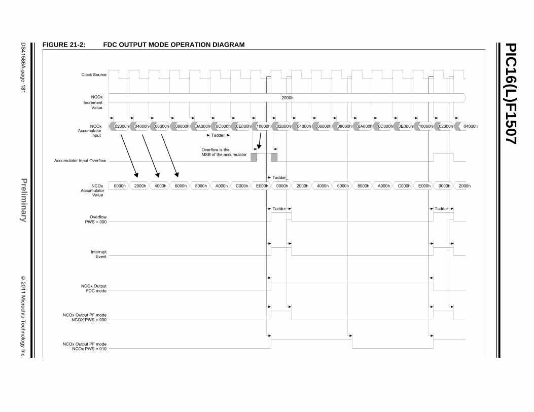
PIC
16(L)F
1507
DS
41
58
6A
-pa
ge
18
1P
relimin
ary
20
11
Micro
chip
Te
chn
olo
gy In
c.
00h 0C000h 0E000h 10000h 02000h 04000h
0h A000h C000h E000h 0000h 2000h
Tadder
FIGURE 21-2: FDC OUTPUT MODE OPERATION DIAGRAM
2000h
02000h 04000h 06000h 08000h 0A000h 0C000h 0E000h 10000h 02000h 04000h 06000h 08000h 0A0
0000h 2000h 4000h 6000h 8000h A000h C000h E000h 0000h 2000h 4000h 6000h 800
Tadder
Tadder_
Overflow is the
Clock Source
NCOx
NCOx
Accumulator Input Overflow
NCOx
Overflow
Interrupt
NCOx Output
NCOx Output PF mode
NCOx Output PF mode
MSB of the accumulator
Tadder
IncrementValue
Input
Value
Accumulator
Accumulator
Event
FDC mode
NCOX PWS = 000
NCOx PWS = 010
PWS = 000
PIC16(L)F1507
21.5 Interrupts
When the accumulator overflows, the NCOx InterruptFlag bit, NCOxIF, of the PIRx register is set. To enablethe interrupt event, the following bits must be set:
• NxEN bit of the NCOxCON register• NCOxIE bit of the PIEx register• PEIE bit of the INTCON register• GIE bit of the INTCON register
The interrupt must be cleared by software by clearingthe NCOxIF bit in the Interrupt Service Routine.
21.6 Effects of a Reset
All of the NCOx registers are cleared to zero as theresult of a Reset.
21.7 Operation In Sleep
The NCO module operates independently from the system clock and will continue to run during Sleep, provided that the clock source selected remains active.
The HFINTOSC remains active during Sleep when the NCO module is enabled and the HFINTOSC is selected as the clock source, regardless of the system clock source selected.
In other words, if the HFINTOSC is simultaneously selected as the system clock and the NCO clock source, when the NCO is enabled, the CPU will go idle during Sleep, but the NCO will continue to operate and the HFINTOSC will remain active.
This will have a direct effect on the Sleep mode current.
21.8 Alternate Pin Locations
This module incorporates I/O pins that can be moved toother locations with the use of the alternate pin functionregister, APFCON. To determine which pins can bemoved and what their default locations are upon aReset, see Section 11.1 “Alternate Pin Function” formore information.
2011 Microchip Technology Inc. Preliminary DS41586A-page 182
PIC16(L)F1507
21.9 NCOx Control Registers
REGISTER 21-2: NCOxCLK: NCOx INPUT CLOCK CONTROL REGISTER
REGISTER 21-1: NCOxCON: NCOx CONTROL REGISTER
R/W-0/0 R/W-0/0 R-0/0 R/W-0/0 U-0 U-0 U-0 R/W-0/0
NxEN NxOE NxOUT NxPOL — — — NxPFM
bit 7 bit 0
Legend:
R = Readable bit W = Writable bit U = Unimplemented bit, read as ‘0’
u = Bit is unchanged x = Bit is unknown -n/n = Value at POR and BOR/Value at all other Resets
‘1’ = Bit is set ‘0’ = Bit is cleared
bit 7 NxEN: NCOx Enable bit1 = NCOx module is enabled0 = NCOx module is disabled
bit 6 NxOE: NCOx Output Enable bit1 = NCOx output pin is enabled0 = NCOx output pin is disabled
bit 5 NxOUT: NCOx Output bit1 = NCOx output is high0 = NCOx output is low
bit 4 NxPOL: NCOx Polarity bit1 = NCOx output signal is active high0 = NCOx output signal is active low
bit 3-1 Unimplemented: Read as ‘0’.
bit 0 NxPFM: NCOx Pulse Frequency Mode bit1 = NCOx operates in Pulse Frequency mode0 = NCOx operates in Fixed Duty Cycle mode
R/W-0/0 R/W-0/0 R/W-0/0 U-0 U-0 U-0 R/W-0/0 R/W-0/0
NxPWS<2:0> — — — NxCKS<1:0>
bit 7 bit 0
Legend:
R = Readable bit W = Writable bit U = Unimplemented bit, read as ‘0’
u = Bit is unchanged x = Bit is unknown -n/n = Value at POR and BOR/Value at all other Resets
‘1’ = Bit is set ‘0’ = Bit is cleared
bit 7-5 NxPWS<2:0>: NCOx Output Pulse Width Select bits(1, 2)
111 = 128 NCOx clock periods110 = 64 NCOx clock periods101 = 32 NCOx clock periods100 = 16 NCOx clock periods011 = 8 NCOx clock periods010 = 4 NCOx clock periods001 = 2 NCOx clock periods000 = 1 NCOx clock periods
bit 4-2 Unimplemented: Read as ‘0’
bit 1-0 NxCKS<1:0>: NCOx Clock Source Select bits11 = NCO1CLK10 = LC1OUT01 = FOSC
00 = HFINTOSC (16 MHz)
Note 1: NxPWS applies only when operating in Pulse Frequency mode.2: If NCOx pulse width is greater than NCOx overflow period, operation is undeterminate.
DS41586A-page 183 Preliminary 2011 Microchip Technology Inc.
PIC16(L)F1507
REGISTER 21-3: NCOxACCL: NCOx ACCUMULATOR REGISTER – LOW BYTE
REGISTER 21-4: NCOxACCH: NCOx ACCUMULATOR REGISTER – HIGH BYTE
REGISTER 21-5: NCOxACCU: NCOx ACCUMULATOR REGISTER – UPPER BYTE
R/W-0/0 R/W-0/0 R/W-0/0 R/W-0/0 R/W-0/0 R/W-0/0 R/W-0/0 R/W-0/0
NCOxACC<7:0>
bit 7 bit 0
Legend:
R = Readable bit W = Writable bit U = Unimplemented bit, read as ‘0’
u = Bit is unchanged x = Bit is unknown -n/n = Value at POR and BOR/Value at all other Resets
‘1’ = Bit is set ‘0’ = Bit is cleared
bit 7-0 NCOxACC<7:0>: NCOx Accumulator, low byte
R/W-0/0 R/W-0/0 R/W-0/0 R/W-0/0 R/W-0/0 R/W-0/0 R/W-0/0 R/W-0/0
NCOxACC<15:8>
bit 7 bit 0
Legend:
R = Readable bit W = Writable bit U = Unimplemented bit, read as ‘0’
u = Bit is unchanged x = Bit is unknown -n/n = Value at POR and BOR/Value at all other Resets
‘1’ = Bit is set ‘0’ = Bit is cleared
bit 7-0 NCOxACC<15:8>: NCOx Accumulator, high byte
U-0 U-0 U-0 U-0 R/W-0/0 R/W-0/0 R/W-0/0 R/W-0/0
— — — — NCOxACC<19:16>
bit 7 bit 0
Legend:
R = Readable bit W = Writable bit U = Unimplemented bit, read as ‘0’
u = Bit is unchanged x = Bit is unknown -n/n = Value at POR and BOR/Value at all other Resets
‘1’ = Bit is set ‘0’ = Bit is cleared
bit 7-4 Unimplemented: Read as ‘0’
bit 3-0 NCOxACC<19:16>: NCOx Accumulator, upper byte
2011 Microchip Technology Inc. Preliminary DS41586A-page 184
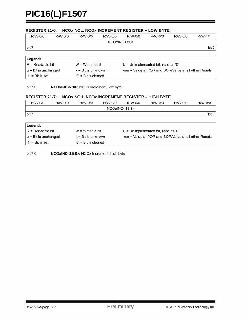
PIC16(L)F1507
REGISTER 21-6: NCOxINCL: NCOx INCREMENT REGISTER – LOW BYTE
REGISTER 21-7: NCOxINCH: NCOx INCREMENT REGISTER – HIGH BYTE
R/W-0/0 R/W-0/0 R/W-0/0 R/W-0/0 R/W-0/0 R/W-0/0 R/W-0/0 R/W-1/1
NCOxINC<7:0>
bit 7 bit 0
Legend:
R = Readable bit W = Writable bit U = Unimplemented bit, read as ‘0’
u = Bit is unchanged x = Bit is unknown -n/n = Value at POR and BOR/Value at all other Resets
‘1’ = Bit is set ‘0’ = Bit is cleared
bit 7-0 NCOxINC<7:0>: NCOx Increment, low byte
R/W-0/0 R/W-0/0 R/W-0/0 R/W-0/0 R/W-0/0 R/W-0/0 R/W-0/0 R/W-0/0
NCOxINC<15:8>
bit 7 bit 0
Legend:
R = Readable bit W = Writable bit U = Unimplemented bit, read as ‘0’
u = Bit is unchanged x = Bit is unknown -n/n = Value at POR and BOR/Value at all other Resets
‘1’ = Bit is set ‘0’ = Bit is cleared
bit 7-0 NCOxINC<15:8>: NCOx Increment, high byte
DS41586A-page 185 Preliminary 2011 Microchip Technology Inc.
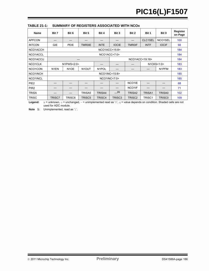
PIC16(L)F1507
TABLE 21-1: SUMMARY OF REGISTERS ASSOCIATED WITH NCOx
Name Bit 7 Bit 6 Bit 5 Bit 4 Bit 3 Bit 2 Bit 1 Bit 0Register on Page
APFCON — — — — — — CLC1SEL NCO1SEL 100
INTCON GIE PEIE TMR0IE INTE IOCIE TMR0IF INTF IOCIF 66
NCO1ACCH NCO1ACC<15:8> 184
NCO1ACCL NCO1ACC<7:0> 184
NCO1ACCU — NCO1ACC<19:16> 184
NCO1CLK N1PWS<2:0> — — — N1CKS<1:0> 183
NCO1CON N1EN N1OE N1OUT N1POL — — — N1PFM 183
NCO1INCH NCO1INC<15:8> 185
NCO1INCL NCO1INC<7:0> 185
PIE2 — — — — — NCO1IE — — 68
PIR2 — — — — — NCO1IF — — 71
TRISA — — TRISA5 TRISA4 —(1) TRISA2 TRISA1 TRISA0 102
TRISC TRISC7 TRISC6 TRISC5 TRISC4 TRISC3 TRISC2 TRISC1 TRISC0 109
Legend: x = unknown, u = unchanged, — = unimplemented read as ‘0’, q = value depends on condition. Shaded cells are not used for ADC module.
Note 1: Unimplemented, read as ‘1’.
2011 Microchip Technology Inc. Preliminary DS41586A-page 186
PIC16(L)F1507
22.0 COMPLEMENTARY WAVEFORM GENERATOR (CWG) MODULE
The Complementary Waveform Generator (CWG) pro-duces a complementary waveform with dead-banddelay from a selection of input sources.
The CWG module has the following features:
• Selectable dead-band clock source control
• Selectable input sources
• Output enable control
• Output polarity control
• Dead-band control with independent 6-bit rising and falling edge dead-band counters
• Auto-shutdown control with:
- Selectable shutdown sources
- Auto-restart enable
- Auto-shutdown pin override control
DS41586A-page 187 Preliminary 2011 Microchip Technology Inc.
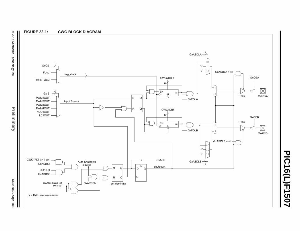
2
01
1 M
icroch
ip T
ech
no
log
y Inc.
Prelim
inary
DS
41
58
6A
-pa
ge
18
8
PIC
16(L)F
1507
FIG
C
0
1
0
1
CWGxA
CWGxB
GxASDLA = 01
GxASDLB = 01
GxOEA
GxOEB
TRISx
TRISx
URE 22-1: CWG BLOCK DIAGRAM
cwg_clock
GxCS
Input SourcePWM1OUTPWM2OUT
NCO1OUT
WG1FLT (INT pin)
GxASDS1
LC2OUT
GxASDS0
FOSC
HFINTOSC
GxIS
LC1OUT
Auto-Shutdown Source
GxPOLA
1
1
3
QS
R Q
ENR
GxARSEN
CWGxDBR
GxPOLB
6
CWGxDBF
00
10
11
‘0’
‘1’
00
10
11
‘0’
‘1’
GxASDLB
2GxASDLA
2
GxASE
=
ENR
6
=
x = CWG module number
PWM3OUTPWM4OUT
QS
R Q
QDS
WRITEGxASE Data Bit
shutdown
set dominate
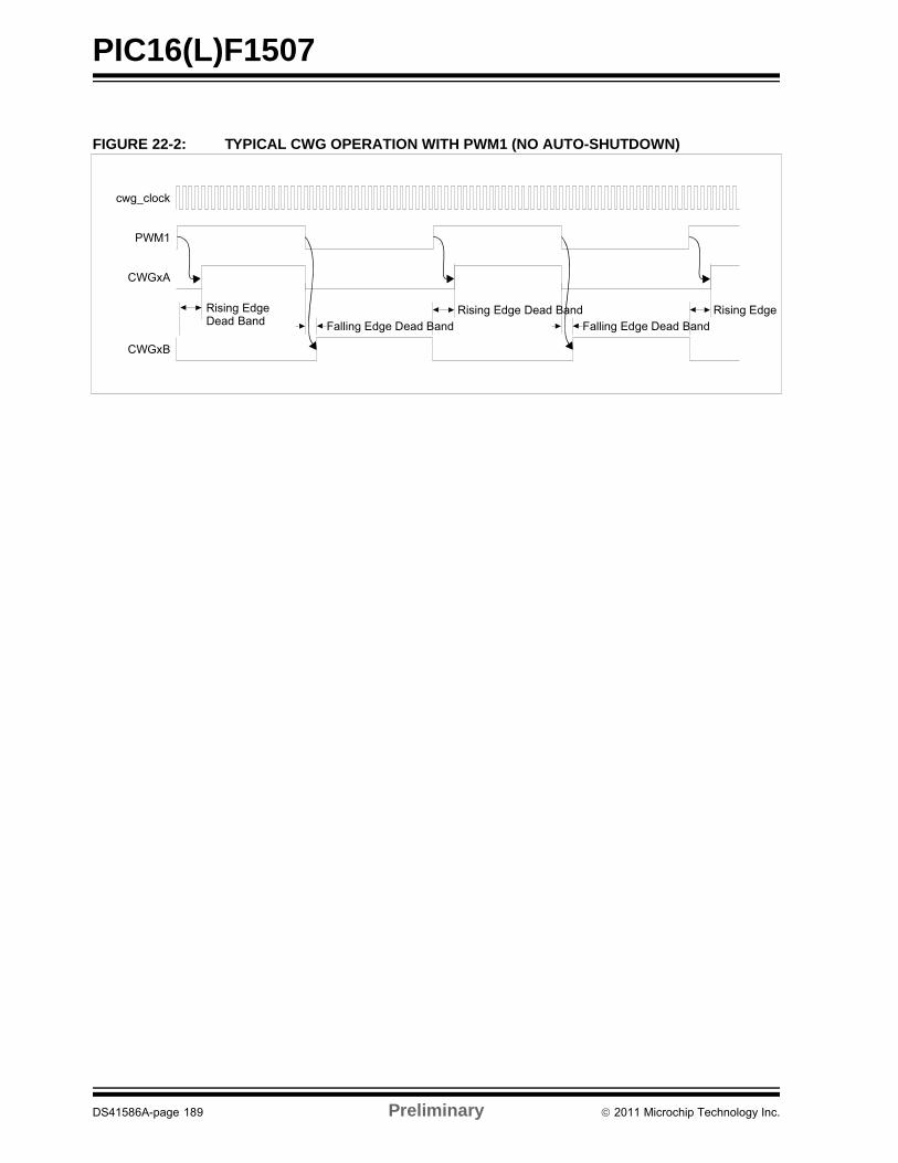
PIC16(L)F1507
FIGURE 22-2: TYPICAL CWG OPERATION WITH PWM1 (NO AUTO-SHUTDOWN)
Rising Edge DFalling Edge Dead Band
Rising Edge Dead BandFalling Edge Dead Band
cwg_clock
PWM1
CWGxA
CWGxB
Rising Edge Dead Band
DS41586A-page 189 Preliminary 2011 Microchip Technology Inc.
PIC16(L)F1507
22.1 Fundamental Operation
The CWG generates a two output complementarywaveform from one of four selectable input sources.
The off-to-on transition of each output can be delayedfrom the on-to-off transition of the other output, thereby,creating a time delay immediately where neither outputis driven. This is referred to as dead time and is coveredin Section 22.5 “Dead-Band Control”. A typicaloperating waveform, with dead band, generated from asingle input signal is shown in Figure 22-2.
It may be necessary to guard against the possibility ofcircuit faults or a feedback event arriving too late or notat all. In this case, the active drive must be terminatedbefore the Fault condition causes damage. This isreferred to as auto-shutdown and is covered inSection 22.9 “Auto-shutdown Control”.
22.2 Clock Source
The CWG module allows for up to 2 different clocksources to be selected:
• Fosc (system clock)• HFINTOSC (16 MHz only)
The clock sources are selected using the G1CS0 bit ofthe CWGxCON0 register (Register 22-1).
22.3 Selectable Input Sources
The CWG uses four different input sources to gener-ate the complementary waveform:
• PWM1• PWM2• PWM3• PWM4• N1OUT• LC1OUT
The input sources are selected using the GxIS<2:0>bits in the CWGxCON1 register (Register 22-2).
22.4 Output Control
Immediately after the CWG module is enabled, thecomplementary drive is configured with both CWGxAand CWGxB drives cleared.
22.4.1 OUTPUT ENABLES
Each CWG output pin has individual output enablecontrol. Output enables are selected with the GxOEAand GxOEB bits of the CWGxCON0 register. When anoutput enable control is cleared, the module asserts nocontrol over the pin. When an output enable is set, theoverride value or active PWM waveform is applied tothe pin per the port priority selection. The output pinenables are dependent on the module enable bit,GxEN. When GxEN is cleared, CWG output enablesand CWG drive levels have no effect.
22.4.2 POLARITY CONTROL
The polarity of each CWG output can be selectedindependently. When the output polarity bit is set, thecorresponding output is active high. Clearing the outputpolarity bit configures the corresponding output asactive low. However, polarity does not affect theoverride levels. Output polarity is selected with theGxPOLA and GxPOLB bits of the CWGxCON0 register.
22.5 Dead-Band Control
Dead-band control provides for non-overlapping outputsignals to prevent shoot through current in powerswitches. The CWG contains two 6-bit dead-bandcounters. One dead-band counter is used for the risingedge of the input source control. The other is used forthe falling edge of the input source control.
Dead band is timed by counting CWG clock periodsfrom zero up to the value in the rising or falling dead-band counter registers. See CWGxDBR andCWGxDBF registers (Register 22-4 and Register 22-5,respectively).
22.6 Rising Edge Dead Band
The rising edge dead-band delays the turn-on of theCWGxA output from when the CWGxB output is turnedoff. The rising edge dead-band time starts when therising edge of the input source signal goes true. Whenthis happens, the CWGxB output is immediately turnedoff and the rising edge dead-band delay time starts.When the rising edge dead-band delay time is reached,the CWGxA output is turned on.
The CWGxDBR register sets the duration of the dead-band interval on the rising edge of the input sourcesignal. This duration is from 0 to 64 counts of dead band.
Dead band is always counted off the edge on the inputsource signal. A count of 0 (zero), indicates that nodead band is present.
If the input source signal is not present for enough timefor the count to be completed, no output will be seen onthe respective output.
2011 Microchip Technology Inc. Preliminary DS41586A-page 190
PIC16(L)F1507
22.7 Falling Edge Dead Band
The falling edge dead band delays the turn-on of theCWGxB output from when the CWGxA output is turnedoff. The falling edge dead-band time starts when thefalling edge of the input source goes true. When thishappens, the CWGxA output is immediately turned offand the falling edge dead-band delay time starts. Whenthe falling edge dead-band delay time is reached, theCWGxB output is turned on.
The CWGxDBF register sets the duration of the dead-band interval on the falling edge of the input source sig-nal. This duration is from 0 to 64 counts of dead band.
Dead band is always counted off the edge on the inputsource signal. A count of 0 (zero), indicates that nodead band is present.
If the input source signal is not present for enough timefor the count to be completed, no output will be seen onthe respective output.
Refer to Figure 22-3 and Figure 22-4 for examples.
22.8 Dead-Band Uncertainty
When the rising and falling edges of the input sourcetriggers the dead-band counters, the input may be asyn-chronous. This will create some uncertainty in the dead-band time delay. The maximum uncertainty is equal toone CWG clock period. Refer to Equation 22-1 for moredetail.
DS41586A-page 191 Preliminary 2011 Microchip Technology Inc.
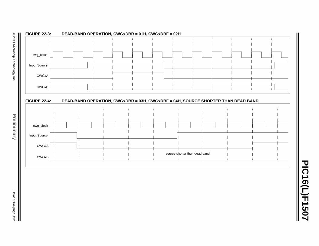
2
01
1 M
icroch
ip T
ech
no
log
y Inc.
Prelim
inary
DS
41
58
6A
-pa
ge
19
2
PIC
16(L)F
1507
FIG
FIG AN DEAD BAND
URE 22-3: DEAD-BAND OPERATION, CWGxDBR = 01H, CWGxDBF = 02H
URE 22-4: DEAD-BAND OPERATION, CWGxDBR = 03H, CWGxDBF = 04H, SOURCE SHORTER TH
Input Source
CWGxA
CWGxB
cwg_clock
source shorter than dead band
Input Source
CWGxA
CWGxB
cwg_clock
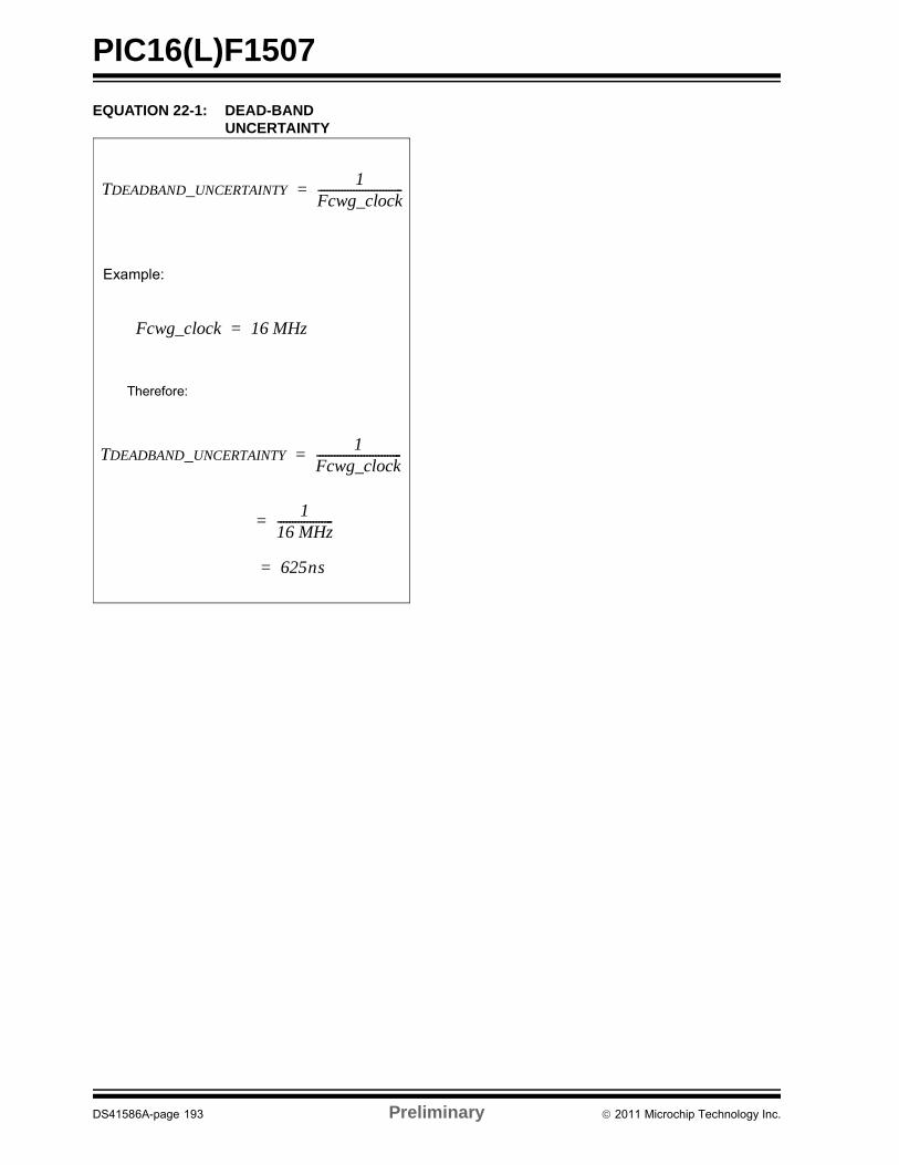
PIC16(L)F1507
EQUATION 22-1: DEAD-BAND UNCERTAINTY
TDEADBAND_UNCERTAINTY1
Fcwg_clock-----------------------------=
Therefore:
Fcwg_clock 16 MHz=
1
16 MHz-------------------=
625ns=
TDEADBAND_UNCERTAINTY1
Fcwg_clock-----------------------------=
Example:
DS41586A-page 193 Preliminary 2011 Microchip Technology Inc.
PIC16(L)F1507
22.9 Auto-shutdown Control
Auto-shutdown is a method to immediately override theCWG output levels with specific overrides that allow forsafe shutdown of the circuit. The shutdown state can beeither cleared automatically or held until cleared bysoftware.
22.9.1 SHUTDOWN
The shutdown state can be entered by either of the fol-lowing two methods:
• Software generated
• External Input
22.9.1.1 Software Generated Shutdown
Setting the GxASE bit of the CWGxCON2 register willforce the CWG into the shutdown state.
When auto-restart is disabled, the shutdown state willpersist as long as the GxASE bit is set.
When auto-restart is enabled, the GxASE bit will clearautomatically and resume operation on the next risingedge event. See Figure 22-6.
22.9.1.2 External Input Source
External shutdown inputs provide the fastest way tosafely suspend CWG operation in the event of a Faultcondition. When any of the selected shutdown inputsgoes active, the CWG outputs will immediately go tothe selected override levels without software delay. Anycombination of two input sources can be selected tocause a shutdown condition. The two sources are:
• LC2OUT
• CWG1FLT
Shutdown inputs are selected using the GxASDS0 andGxASDS1 bits of the CWGxCON2 register.(Register 22-3).
22.10 Operation During Sleep
The CWG module operates independently from the system clock and will continue to run during Sleep, provided that the clock and input sources selected remain active.
The HFINTOSC remains active during Sleep, provided that the CWG module is enabled, the input source is active, and the HFINTOSC is selected as the clock source, regardless of the system clock source selected.
In other words, if the HFINTOSC is simultaneously selected as the system clock and the CWG clock source, when the CWG is enabled and the input source is active, the CPU will go idle during Sleep, but the CWG will continue to operate and the HFINTOSC will remain active.
This will have a direct effect on the Sleep mode current.
Note: Shutdown inputs are level sensitive, notedge sensitive. The shutdown state can-not be cleared, except by disabling auto-shutdown, as long as the shutdown inputlevel persists.
2011 Microchip Technology Inc. Preliminary DS41586A-page 194
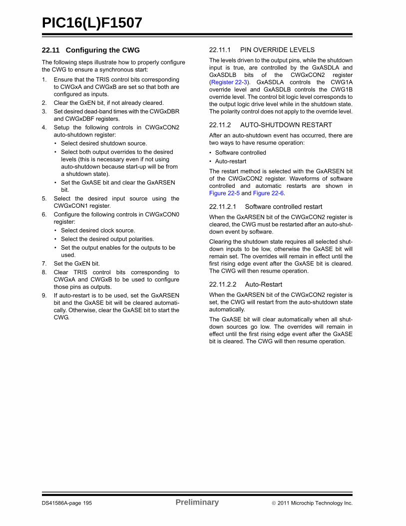
PIC16(L)F1507
22.11 Configuring the CWG
The following steps illustrate how to properly configurethe CWG to ensure a synchronous start:
1. Ensure that the TRIS control bits correspondingto CWGxA and CWGxB are set so that both areconfigured as inputs.
2. Clear the GxEN bit, if not already cleared.
3. Set desired dead-band times with the CWGxDBRand CWGxDBF registers.
4. Setup the following controls in CWGxCON2auto-shutdown register:
• Select desired shutdown source.
• Select both output overrides to the desired levels (this is necessary even if not using auto-shutdown because start-up will be from a shutdown state).
• Set the GxASE bit and clear the GxARSEN bit.
5. Select the desired input source using theCWGxCON1 register.
6. Configure the following controls in CWGxCON0register:
• Select desired clock source.
• Select the desired output polarities.
• Set the output enables for the outputs to be used.
7. Set the GxEN bit.
8. Clear TRIS control bits corresponding toCWGxA and CWGxB to be used to configurethose pins as outputs.
9. If auto-restart is to be used, set the GxARSENbit and the GxASE bit will be cleared automati-cally. Otherwise, clear the GxASE bit to start theCWG.
22.11.1 PIN OVERRIDE LEVELS
The levels driven to the output pins, while the shutdowninput is true, are controlled by the GxASDLA andGxASDLB bits of the CWGxCON2 register(Register 22-3). GxASDLA controls the CWG1Aoverride level and GxASDLB controls the CWG1Boverride level. The control bit logic level corresponds tothe output logic drive level while in the shutdown state.The polarity control does not apply to the override level.
22.11.2 AUTO-SHUTDOWN RESTART
After an auto-shutdown event has occurred, there aretwo ways to have resume operation:
• Software controlled
• Auto-restart
The restart method is selected with the GxARSEN bitof the CWGxCON2 register. Waveforms of softwarecontrolled and automatic restarts are shown inFigure 22-5 and Figure 22-6.
22.11.2.1 Software controlled restart
When the GxARSEN bit of the CWGxCON2 register iscleared, the CWG must be restarted after an auto-shut-down event by software.
Clearing the shutdown state requires all selected shut-down inputs to be low, otherwise the GxASE bit willremain set. The overrides will remain in effect until thefirst rising edge event after the GxASE bit is cleared.The CWG will then resume operation.
22.11.2.2 Auto-Restart
When the GxARSEN bit of the CWGxCON2 register isset, the CWG will restart from the auto-shutdown stateautomatically.
The GxASE bit will clear automatically when all shut-down sources go low. The overrides will remain ineffect until the first rising edge event after the GxASEbit is cleared. The CWG will then resume operation.
DS41586A-page 195 Preliminary 2011 Microchip Technology Inc.
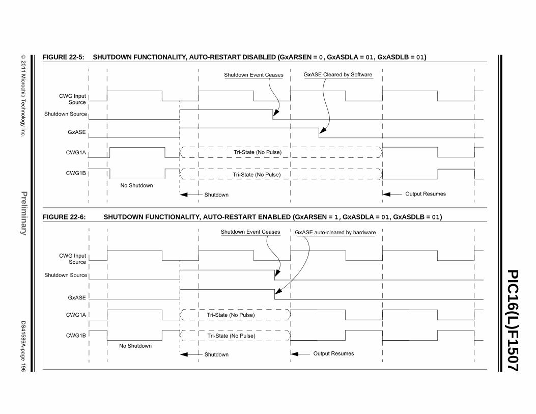
2
01
1 M
icroch
ip T
ech
no
log
y Inc.
Prelim
inary
DS
41
58
6A
-pa
ge
19
6
PIC
16(L)F
1507
FIG xASDLB = 01)
FIG 01, GxASDLB = 01)
Output Resumes
Sh
Sh
URE 22-5: SHUTDOWN FUNCTIONALITY, AUTO-RESTART DISABLED (GxARSEN = 0,GxASDLA = 01, G
URE 22-6: SHUTDOWN FUNCTIONALITY, AUTO-RESTART ENABLED (GxARSEN = 1,GxASDLA =
Shutdown
GxASE Cleared by Software
No Shutdown
CWG Input
GxASE
CWG1A
Source
utdown Source
Shutdown Event Ceases
Tri-State (No Pulse)
CWG1B Tri-State (No Pulse)
Shutdown
Tri-State (No Pulse)
GxASE auto-cleared by hardware
Output Resumes
No Shutdown
CWG Input
GxASE
CWG1A
Source
utdown Source
Shutdown Event Ceases
CWG1B
Tri-State (No Pulse)
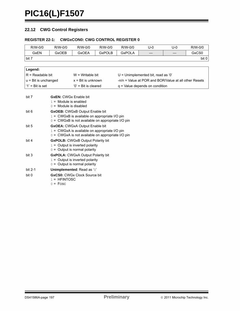
PIC16(L)F1507
22.12 CWG Control Registers
REGISTER 22-1: CWGxCON0: CWG CONTROL REGISTER 0
R/W-0/0 R/W-0/0 R/W-0/0 R/W-0/0 R/W-0/0 U-0 U-0 R/W-0/0
GxEN GxOEB GxOEA GxPOLB GxPOLA — — GxCS0
bit 7 bit 0
Legend:
R = Readable bit W = Writable bit U = Unimplemented bit, read as ‘0’
u = Bit is unchanged x = Bit is unknown -n/n = Value at POR and BOR/Value at all other Resets
‘1’ = Bit is set ‘0’ = Bit is cleared q = Value depends on condition
bit 7 GxEN: CWGx Enable bit1 = Module is enabled0 = Module is disabled
bit 6 GxOEB: CWGxB Output Enable bit1 = CWGxB is available on appropriate I/O pin0 = CWGxB is not available on appropriate I/O pin
bit 5 GxOEA: CWGxA Output Enable bit1 = CWGxA is available on appropriate I/O pin 0 = CWGxA is not available on appropriate I/O pin
bit 4 GxPOLB: CWGxB Output Polarity bit1 = Output is inverted polarity0 = Output is normal polarity
bit 3 GxPOLA: CWGxA Output Polarity bit1 = Output is inverted polarity0 = Output is normal polarity
bit 2-1 Unimplemented: Read as ‘0’
bit 0 GxCS0: CWGx Clock Source bit1 = HFINTOSC0 = FOSC
DS41586A-page 197 Preliminary 2011 Microchip Technology Inc.
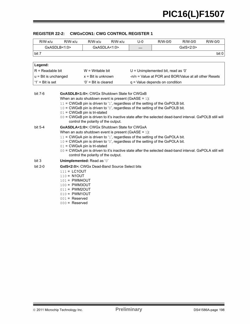
PIC16(L)F1507
REGISTER 22-2: CWGxCON1: CWG CONTROL REGISTER 1
R/W-x/u R/W-x/u R/W-x/u R/W-x/u U-0 R/W-0/0 R/W-0/0 R/W-0/0
GxASDLB<1:0> GxASDLA<1:0> — GxIS<2:0>
bit 7 bit 0
Legend:
R = Readable bit W = Writable bit U = Unimplemented bit, read as ‘0’
u = Bit is unchanged x = Bit is unknown -n/n = Value at POR and BOR/Value at all other Resets
‘1’ = Bit is set ‘0’ = Bit is cleared q = Value depends on condition
bit 7-6 GxASDLB<1:0>: CWGx Shutdown State for CWGxBWhen an auto shutdown event is present (GxASE = 1):11 = CWGxB pin is driven to ‘1’, regardless of the setting of the GxPOLB bit.10 = CWGxB pin is driven to ‘0’, regardless of the setting of the GxPOLB bit.01 = CWGxB pin is tri-stated00 = CWGxB pin is driven to it’s inactive state after the selected dead-band interval. GxPOLB still will
control the polarity of the output.
bit 5-4 GxASDLA<1:0>: CWGx Shutdown State for CWGxAWhen an auto shutdown event is present (GxASE = 1):11 = CWGxA pin is driven to ‘1’, regardless of the setting of the GxPOLA bit.10 = CWGxA pin is driven to ‘0’, regardless of the setting of the GxPOLA bit.01 = CWGxA pin is tri-stated00 = CWGxA pin is driven to it’s inactive state after the selected dead-band interval. GxPOLA still will
control the polarity of the output.
bit 3 Unimplemented: Read as ‘0’
bit 2-0 GxIS<2:0>: CWGx Dead-Band Source Select bits111 = LC1OUT110 = N1OUT101 = PWM4OUT100 = PWM3OUT011 = PWM2OUT010 = PWM1OUT001 = Reserved000 = Reserved
2011 Microchip Technology Inc. Preliminary DS41586A-page 198
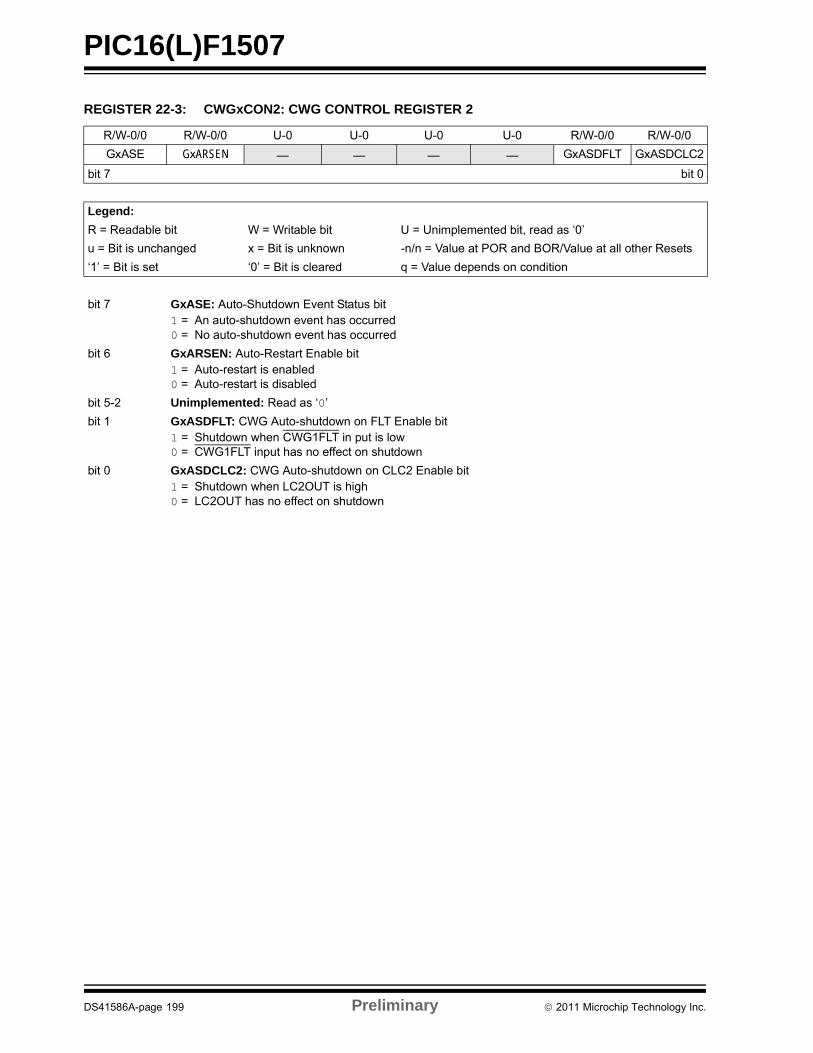
PIC16(L)F1507
REGISTER 22-3: CWGxCON2: CWG CONTROL REGISTER 2
R/W-0/0 R/W-0/0 U-0 U-0 U-0 U-0 R/W-0/0 R/W-0/0
GxASE GxARSEN — — — — GxASDFLT GxASDCLC2
bit 7 bit 0
Legend:
R = Readable bit W = Writable bit U = Unimplemented bit, read as ‘0’
u = Bit is unchanged x = Bit is unknown -n/n = Value at POR and BOR/Value at all other Resets
‘1’ = Bit is set ‘0’ = Bit is cleared q = Value depends on condition
bit 7 GxASE: Auto-Shutdown Event Status bit1 = An auto-shutdown event has occurred0 = No auto-shutdown event has occurred
bit 6 GxARSEN: Auto-Restart Enable bit1 = Auto-restart is enabled0 = Auto-restart is disabled
bit 5-2 Unimplemented: Read as ‘0’
bit 1 GxASDFLT: CWG Auto-shutdown on FLT Enable bit1 = Shutdown when CWG1FLT in put is low0 = CWG1FLT input has no effect on shutdown
bit 0 GxASDCLC2: CWG Auto-shutdown on CLC2 Enable bit1 = Shutdown when LC2OUT is high0 = LC2OUT has no effect on shutdown
DS41586A-page 199 Preliminary 2011 Microchip Technology Inc.
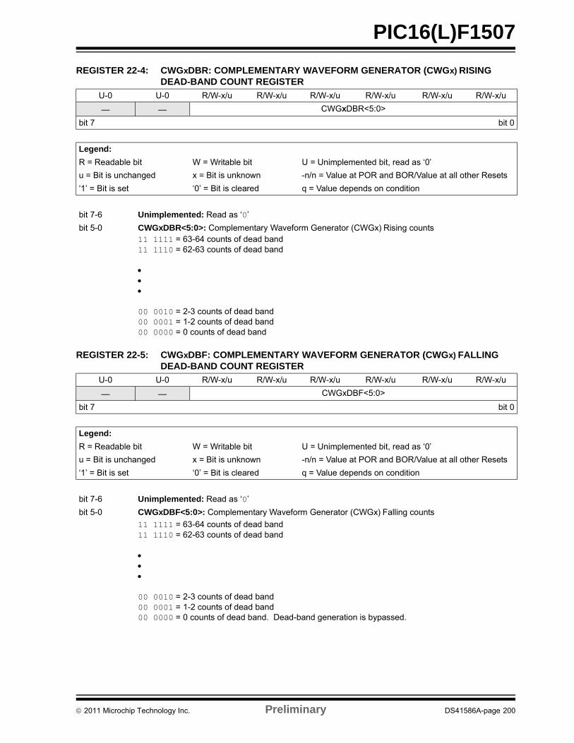
PIC16(L)F1507
REGISTER 22-4: CWGxDBR: COMPLEMENTARY WAVEFORM GENERATOR (CWGx) RISING DEAD-BAND COUNT REGISTER
REGISTER 22-5: CWGxDBF: COMPLEMENTARY WAVEFORM GENERATOR (CWGx) FALLING DEAD-BAND COUNT REGISTER
U-0 U-0 R/W-x/u R/W-x/u R/W-x/u R/W-x/u R/W-x/u R/W-x/u
— — CWGxDBR<5:0>
bit 7 bit 0
Legend:
R = Readable bit W = Writable bit U = Unimplemented bit, read as ‘0’
u = Bit is unchanged x = Bit is unknown -n/n = Value at POR and BOR/Value at all other Resets
‘1’ = Bit is set ‘0’ = Bit is cleared q = Value depends on condition
bit 7-6 Unimplemented: Read as ‘0’
bit 5-0 CWGxDBR<5:0>: Complementary Waveform Generator (CWGx) Rising counts11 1111 = 63-64 counts of dead band11 1110 = 62-63 counts of dead band
00 0010 = 2-3 counts of dead band00 0001 = 1-2 counts of dead band00 0000 = 0 counts of dead band
U-0 U-0 R/W-x/u R/W-x/u R/W-x/u R/W-x/u R/W-x/u R/W-x/u
— — CWGxDBF<5:0>
bit 7 bit 0
Legend:
R = Readable bit W = Writable bit U = Unimplemented bit, read as ‘0’
u = Bit is unchanged x = Bit is unknown -n/n = Value at POR and BOR/Value at all other Resets
‘1’ = Bit is set ‘0’ = Bit is cleared q = Value depends on condition
bit 7-6 Unimplemented: Read as ‘0’
bit 5-0 CWGxDBF<5:0>: Complementary Waveform Generator (CWGx) Falling counts
11 1111 = 63-64 counts of dead band11 1110 = 62-63 counts of dead band
00 0010 = 2-3 counts of dead band00 0001 = 1-2 counts of dead band00 0000 = 0 counts of dead band. Dead-band generation is bypassed.
2011 Microchip Technology Inc. Preliminary DS41586A-page 200
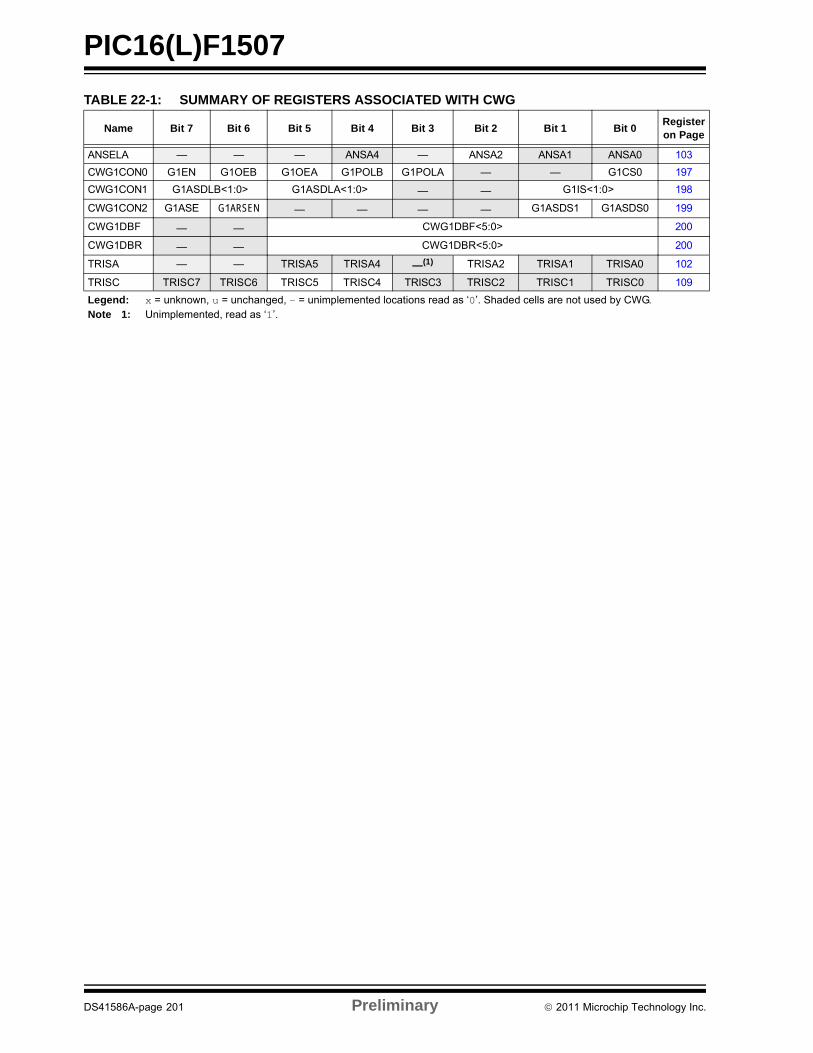
PIC16(L)F1507
TABLE 22-1: SUMMARY OF REGISTERS ASSOCIATED WITH CWG
Name Bit 7 Bit 6 Bit 5 Bit 4 Bit 3 Bit 2 Bit 1 Bit 0Register on Page
ANSELA — — — ANSA4 — ANSA2 ANSA1 ANSA0 103
CWG1CON0 G1EN G1OEB G1OEA G1POLB G1POLA — — G1CS0 197
CWG1CON1 G1ASDLB<1:0> G1ASDLA<1:0> — — G1IS<1:0> 198
CWG1CON2 G1ASE G1ARSEN — — — — G1ASDS1 G1ASDS0 199
CWG1DBF — — CWG1DBF<5:0> 200
CWG1DBR — — CWG1DBR<5:0> 200
TRISA — — TRISA5 TRISA4 —(1) TRISA2 TRISA1 TRISA0 102
TRISC TRISC7 TRISC6 TRISC5 TRISC4 TRISC3 TRISC2 TRISC1 TRISC0 109
Legend: x = unknown, u = unchanged, – = unimplemented locations read as ‘0’. Shaded cells are not used by CWG.Note 1: Unimplemented, read as ‘1’.
DS41586A-page 201 Preliminary 2011 Microchip Technology Inc.

PIC16(L)F1507
NOTES:
2011 Microchip Technology Inc. Preliminary DS41586A-page 202
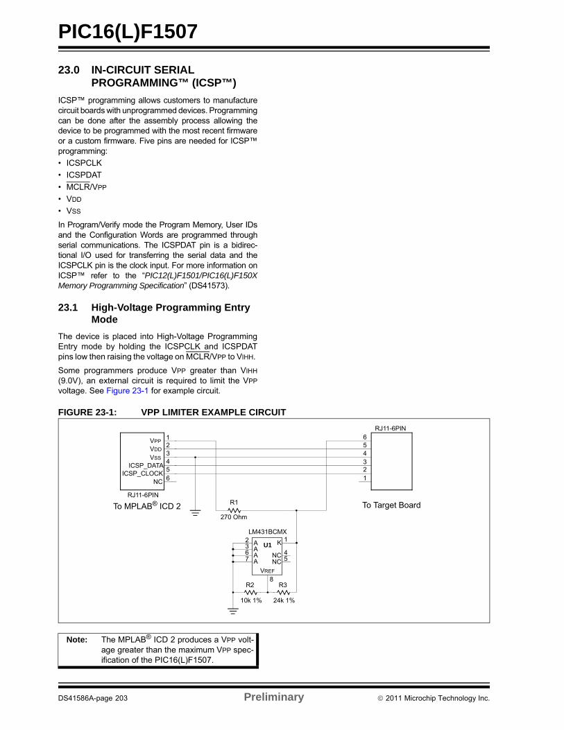
PIC16(L)F1507
23.0 IN-CIRCUIT SERIAL PROGRAMMING™ (ICSP™)
ICSP™ programming allows customers to manufacturecircuit boards with unprogrammed devices. Programmingcan be done after the assembly process allowing thedevice to be programmed with the most recent firmwareor a custom firmware. Five pins are needed for ICSP™programming:
• ICSPCLK
• ICSPDAT
• MCLR/VPP
• VDD
• VSS
In Program/Verify mode the Program Memory, User IDsand the Configuration Words are programmed throughserial communications. The ICSPDAT pin is a bidirec-tional I/O used for transferring the serial data and theICSPCLK pin is the clock input. For more information onICSP™ refer to the “PIC12(L)F1501/PIC16(L)F150XMemory Programming Specification” (DS41573).
23.1 High-Voltage Programming Entry Mode
The device is placed into High-Voltage ProgrammingEntry mode by holding the ICSPCLK and ICSPDATpins low then raising the voltage on MCLR/VPP to VIHH.
Some programmers produce VPP greater than VIHH
(9.0V), an external circuit is required to limit the VPP
voltage. See Figure 23-1 for example circuit.
FIGURE 23-1: VPP LIMITER EXAMPLE CIRCUIT
VREF
VPP
VDD
VSS
ICSP_DATAICSP_CLOCK
NC
RJ11-6PIN
RJ11-6PIN
R1
270 Ohm
To MPLAB® ICD 2 To Target Board
123456 1
23456
R2 R3
10k 1% 24k 1%
U1
LM431BCMX
A2367
8
AAA
K
NCNC
1
45
Note: The MPLAB® ICD 2 produces a VPP volt-age greater than the maximum VPP spec-ification of the PIC16(L)F1507.
DS41586A-page 203 Preliminary 2011 Microchip Technology Inc.
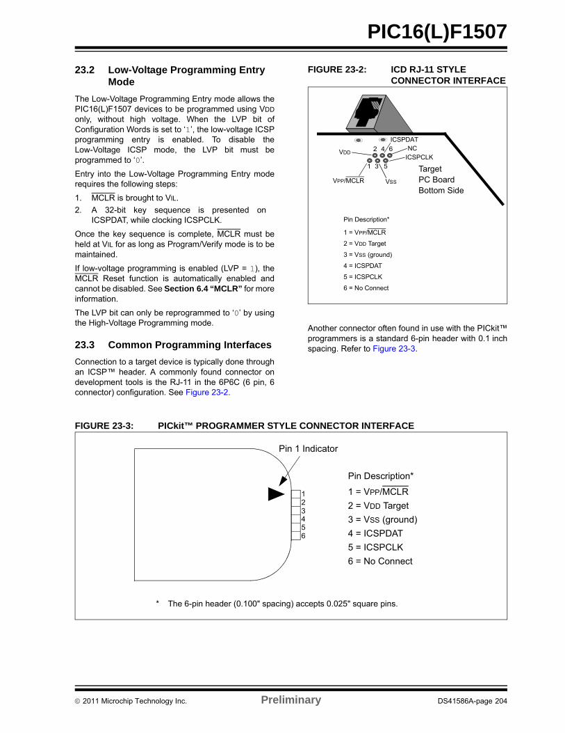
PIC16(L)F1507
23.2 Low-Voltage Programming Entry Mode
The Low-Voltage Programming Entry mode allows thePIC16(L)F1507 devices to be programmed using VDD
only, without high voltage. When the LVP bit ofConfiguration Words is set to ‘1’, the low-voltage ICSPprogramming entry is enabled. To disable theLow-Voltage ICSP mode, the LVP bit must beprogrammed to ‘0’.
Entry into the Low-Voltage Programming Entry moderequires the following steps:
1. MCLR is brought to VIL.
2. A 32-bit key sequence is presented onICSPDAT, while clocking ICSPCLK.
Once the key sequence is complete, MCLR must beheld at VIL for as long as Program/Verify mode is to bemaintained.
If low-voltage programming is enabled (LVP = 1), theMCLR Reset function is automatically enabled andcannot be disabled. See Section 6.4 “MCLR” for moreinformation.
The LVP bit can only be reprogrammed to ‘0’ by usingthe High-Voltage Programming mode.
23.3 Common Programming Interfaces
Connection to a target device is typically done throughan ICSP™ header. A commonly found connector ondevelopment tools is the RJ-11 in the 6P6C (6 pin, 6connector) configuration. See Figure 23-2.
FIGURE 23-2: ICD RJ-11 STYLE CONNECTOR INTERFACE
Another connector often found in use with the PICkit™programmers is a standard 6-pin header with 0.1 inchspacing. Refer to Figure 23-3.
FIGURE 23-3: PICkit™ PROGRAMMER STYLE CONNECTOR INTERFACE
1
2
3
4
5
6
Target
Bottom SidePC BoardVPP/MCLR VSS
ICSPCLKVDD
ICSPDATNC
Pin Description*
1 = VPP/MCLR
2 = VDD Target
3 = VSS (ground)
4 = ICSPDAT
5 = ICSPCLK
6 = No Connect
123456
* The 6-pin header (0.100" spacing) accepts 0.025" square pins.
Pin Description*
1 = VPP/MCLR
2 = VDD Target
3 = VSS (ground)
4 = ICSPDAT
5 = ICSPCLK
6 = No Connect
Pin 1 Indicator
2011 Microchip Technology Inc. Preliminary DS41586A-page 204
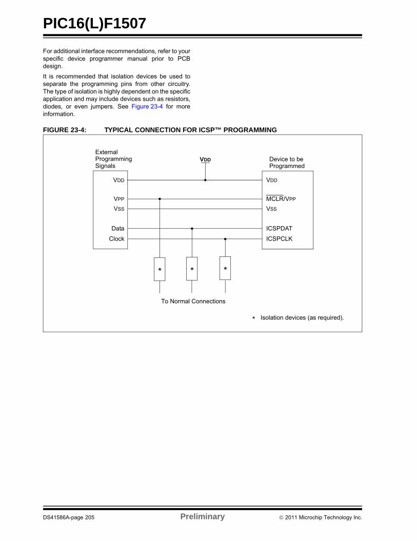
PIC16(L)F1507
For additional interface recommendations, refer to yourspecific device programmer manual prior to PCBdesign.
It is recommended that isolation devices be used toseparate the programming pins from other circuitry.The type of isolation is highly dependent on the specificapplication and may include devices such as resistors,diodes, or even jumpers. See Figure 23-4 for moreinformation.
FIGURE 23-4: TYPICAL CONNECTION FOR ICSP™ PROGRAMMING
VDD
VPP
VSS
ExternalDevice to be
Data
Clock
VDD
MCLR/VPP
VSS
ICSPDAT
ICSPCLK
* **
To Normal Connections
* Isolation devices (as required).
Programming Signals Programmed
VDD
DS41586A-page 205 Preliminary 2011 Microchip Technology Inc.

PIC16(L)F1507
NOTES:
2011 Microchip Technology Inc. Preliminary DS41586A-page 206
PIC16(L)F1507
24.0 INSTRUCTION SET SUMMARY
Each PIC16 instruction is a 14-bit word containing theoperation code (opcode) and all required operands.The op codes are broken into three broad categories.
• Byte Oriented
• Bit Oriented
• Literal and Control
The literal and control category contains the most var-ied instruction word format.
Table 24-3 lists the instructions recognized by theMPASMTM assembler.
All instructions are executed within a single instructioncycle, with the following exceptions, which may taketwo or three cycles:
• Subroutine takes two cycles (CALL, CALLW)• Returns from interrupts or subroutines take two
cycles (RETURN, RETLW, RETFIE)• Program branching takes two cycles (GOTO, BRA, BRW, BTFSS, BTFSC, DECFSZ, INCSFZ)
• One additional instruction cycle will be used when any instruction references an indirect file register and the file select register is pointing to program memory.
One instruction cycle consists of 4 oscillator cycles; foran oscillator frequency of 4 MHz, this gives a nominalinstruction execution rate of 1 MHz.
All instruction examples use the format ‘0xhh’ torepresent a hexadecimal number, where ‘h’ signifies ahexadecimal digit.
24.1 Read-Modify-Write Operations
Any instruction that specifies a file register as part ofthe instruction performs a Read-Modify-Write (R-M-W)operation. The register is read, the data is modified,and the result is stored according to either the instruc-tion, or the destination designator ‘d’. A read operationis performed on a register even if the instruction writesto that register.
TABLE 24-1: OPCODE FIELD DESCRIPTIONS
TABLE 24-2: ABBREVIATION DESCRIPTIONS
Field Description
f Register file address (0x00 to 0x7F)
W Working register (accumulator)
b Bit address within an 8-bit file register
k Literal field, constant data or label
x Don’t care location (= 0 or 1). The assembler will generate code with x = 0. It is the recommended form of use for compatibility with all Microchip software tools.
d Destination select; d = 0: store result in W,d = 1: store result in file register f. Default is d = 1.
n FSR or INDF number. (0-1)
mm Pre-post increment-decrement mode selection
Field Description
PC Program Counter
TO Time-out bit
C Carry bit
DC Digit carry bit
Z Zero bit
PD Power-down bit
DS41586A-page 207 Preliminary 2011 Microchip Technology Inc.
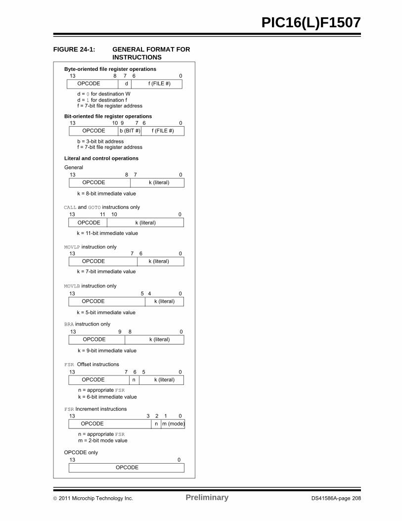
PIC16(L)F1507
FIGURE 24-1: GENERAL FORMAT FOR INSTRUCTIONS
Byte-oriented file register operations13 8 7 6 0
d = 0 for destination W
OPCODE d f (FILE #)
d = 1 for destination ff = 7-bit file register address
Bit-oriented file register operations13 10 9 7 6 0
OPCODE b (BIT #) f (FILE #)
b = 3-bit bit addressf = 7-bit file register address
Literal and control operations
13 8 7 0
OPCODE k (literal)
k = 8-bit immediate value
13 11 10 0
OPCODE k (literal)
k = 11-bit immediate value
General
CALL and GOTO instructions only
MOVLP instruction only
13 5 4 0
OPCODE k (literal)
k = 5-bit immediate value
MOVLB instruction only
13 9 8 0
OPCODE k (literal)
k = 9-bit immediate value
BRA instruction only
FSR Offset instructions
13 7 6 5 0
OPCODE n k (literal)
n = appropriate FSR
FSR Increment instructions
13 7 6 0
OPCODE k (literal)
k = 7-bit immediate value
13 3 2 1 0
OPCODE n m (mode)
n = appropriate FSRm = 2-bit mode value
k = 6-bit immediate value
13 0
OPCODE
OPCODE only
2011 Microchip Technology Inc. Preliminary DS41586A-page 208
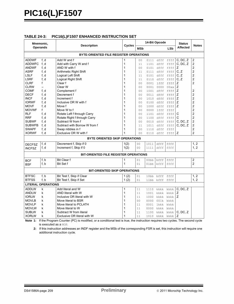
PIC16(L)F1507
TABLE 24-3: PIC16(L)F1507 ENHANCED INSTRUCTION SET
Mnemonic,Operands
Description Cycles14-Bit Opcode Status
AffectedNotes
MSb LSb
BYTE-ORIENTED FILE REGISTER OPERATIONS
ADDWFADDWFCANDWFASRFLSLFLSRFCLRFCLRWCOMFDECFINCFIORWFMOVFMOVWFRLFRRFSUBWFSUBWFBSWAPFXORWF
f, df, df, df, df, df, df–f, df, df, df, df, dff, df, df, df, df, df, d
Add W and fAdd with Carry W and fAND W with fArithmetic Right ShiftLogical Left ShiftLogical Right ShiftClear fClear WComplement fDecrement fIncrement fInclusive OR W with fMove fMove W to fRotate Left f through CarryRotate Right f through CarrySubtract W from fSubtract with Borrow W from fSwap nibbles in fExclusive OR W with f
11111111111111111111
0011001111110000000000000000000000110000
01111101010101110101011000010001100100111010010010000000110111000010101111100110
dfffdfffdfffdfffdfffdffflfff0000dfffdfffdfffdfffdfff1fffdfffdfffdfffdfffdfffdfff
ffffffffffffffffffffffffffff00xxffffffffffffffffffffffffffffffffffffffffffffffff
C, DC, ZC, DC, ZZC, ZC, ZC, ZZZZZZZZ
CCC, DC, ZC, DC, Z
Z
2222222
222222222222
BYTE ORIENTED SKIP OPERATIONS
DECFSZINCFSZ
f, df, d
Decrement f, Skip if 0Increment f, Skip if 0
1(2)1(2)
0000
10111111
dfffdfff
ffffffff
1, 21, 2
BIT-ORIENTED FILE REGISTER OPERATIONS
BCFBSF
f, bf, b
Bit Clear fBit Set f
11
0101
00bb01bb
bfffbfff
ffffffff
22
BIT-ORIENTED SKIP OPERATIONS
BTFSCBTFSS
f, bf, b
Bit Test f, Skip if ClearBit Test f, Skip if Set
1 (2)1 (2)
0101
10bb11bb
bfff bfff
ffffffff
1, 21, 2
LITERAL OPERATIONS
ADDLWANDLWIORLWMOVLBMOVLPMOVLWSUBLWXORLW
kkkkkkkk
Add literal and WAND literal with WInclusive OR literal with WMove literal to BSRMove literal to PCLATHMove literal to WSubtract W from literalExclusive OR literal with W
11111111
1111110011111111
11101001100000000001000011001010
kkkkkkkkkkkk001k1kkkkkkkkkkkkkkk
kkkkkkkkkkkkkkkkkkkkkkkkkkkkkkkk
C, DC, ZZZ
C, DC, ZZ
Note 1: If the Program Counter (PC) is modified, or a conditional test is true, the instruction requires two cycles. The second cycle is executed as a NOP.
2: If this instruction addresses an INDF register and the MSb of the corresponding FSR is set, this instruction will require one additional instruction cycle.
DS41586A-page 209 Preliminary 2011 Microchip Technology Inc.
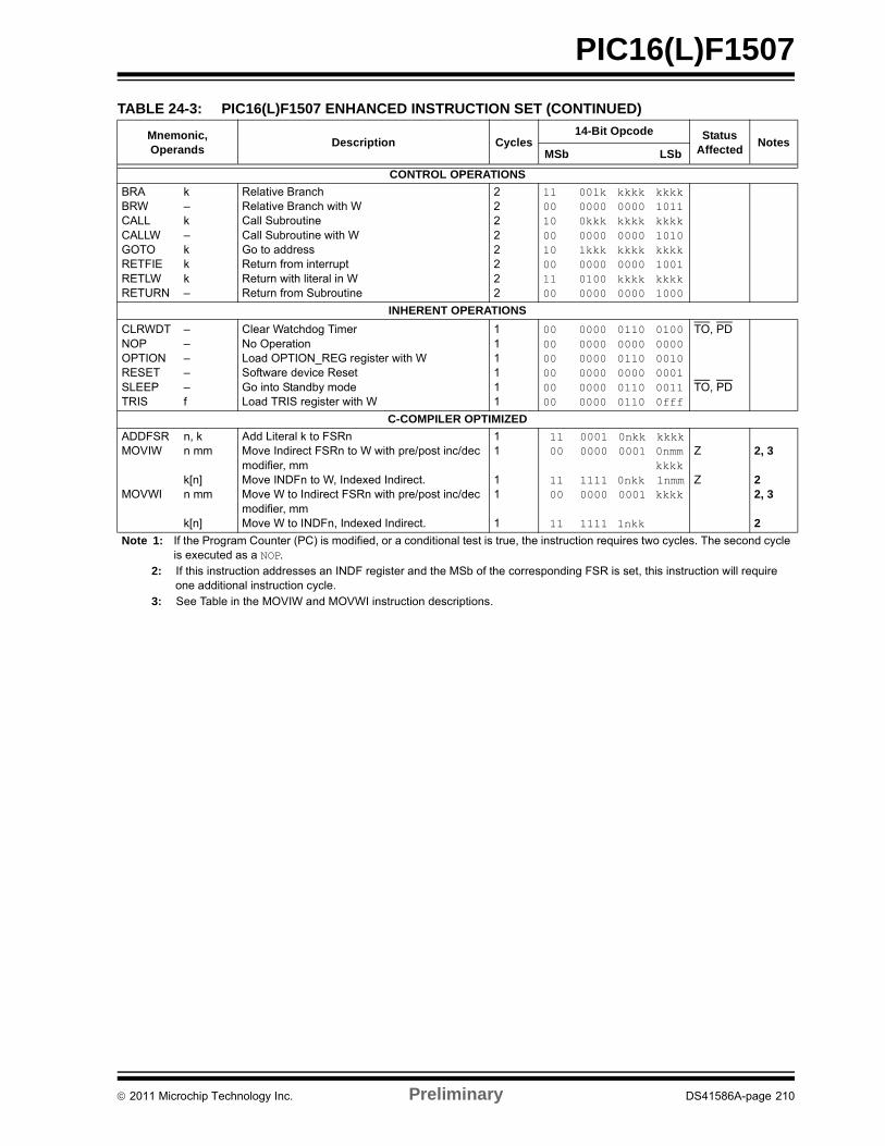
PIC16(L)F1507
TABLE 24-3: PIC16(L)F1507 ENHANCED INSTRUCTION SET (CONTINUED)
Mnemonic,Operands
Description Cycles14-Bit Opcode Status
AffectedNotes
MSb LSb
CONTROL OPERATIONS
BRABRWCALLCALLWGOTORETFIERETLWRETURN
k–k–kkk–
Relative BranchRelative Branch with WCall SubroutineCall Subroutine with WGo to addressReturn from interruptReturn with literal in WReturn from Subroutine
22222222
1100100010001100
001k00000kkk00001kkk000001000000
kkkk0000kkkk0000kkkk0000kkkk0000
kkkk1011kkkk1010kkkk1001kkkk1000
INHERENT OPERATIONS
CLRWDTNOPOPTIONRESETSLEEPTRIS
–––––f
Clear Watchdog TimerNo OperationLoad OPTION_REG register with WSoftware device ResetGo into Standby modeLoad TRIS register with W
111111
000000000000
000000000000000000000000
011000000110000001100110
010000000010000100110fff
TO, PD
TO, PD
C-COMPILER OPTIMIZED
ADDFSRMOVIW
MOVWI
n, kn mm
k[n]n mm
k[n]
Add Literal k to FSRnMove Indirect FSRn to W with pre/post inc/dec modifier, mmMove INDFn to W, Indexed Indirect.Move W to Indirect FSRn with pre/post inc/dec modifier, mmMove W to INDFn, Indexed Indirect.
11
11
1
1100
1100
11
00010000
11110000
1111
0nkk0001
0nkk0001
1nkk
kkkk0nmmkkkk1nmmkkkk
Z
Z
2, 3
22, 3
2
Note 1: If the Program Counter (PC) is modified, or a conditional test is true, the instruction requires two cycles. The second cycle is executed as a NOP.
2: If this instruction addresses an INDF register and the MSb of the corresponding FSR is set, this instruction will require one additional instruction cycle.
3: See Table in the MOVIW and MOVWI instruction descriptions.
2011 Microchip Technology Inc. Preliminary DS41586A-page 210
PIC16(L)F1507
24.2 Instruction Descriptions
ADDFSR Add Literal to FSRn
Syntax: [ label ] ADDFSR FSRn, k
Operands: -32 k 31n [ 0, 1]
Operation: FSR(n) + k FSR(n)
Status Affected: None
Description: The signed 6-bit literal ‘k’ is added to the contents of the FSRnH:FSRnL register pair.
FSRn is limited to the range 0000h - FFFFh. Moving beyond these bounds will cause the FSR to wrap around.
ADDLW Add literal and W
Syntax: [ label ] ADDLW k
Operands: 0 k 255
Operation: (W) + k (W)
Status Affected: C, DC, Z
Description: The contents of the W register are added to the eight-bit literal ‘k’ and the result is placed in the W register.
ADDWF Add W and f
Syntax: [ label ] ADDWF f,d
Operands: 0 f 127d 0,1
Operation: (W) + (f) (destination)
Status Affected: C, DC, Z
Description: Add the contents of the W register with register ‘f’. If ‘d’ is ‘0’, the result is stored in the W register. If ‘d’ is ‘1’, the result is stored back in register ‘f’.
ADDWFC ADD W and CARRY bit to f
Syntax: [ label ] ADDWFC f {,d}
Operands: 0 f 127d [0,1]
Operation: (W) + (f) + (C) dest
Status Affected: C, DC, Z
Description: Add W, the Carry flag and data mem-ory location ‘f’. If ‘d’ is ‘0’, the result is placed in W. If ‘d’ is ‘1’, the result is placed in data memory location ‘f’.
ANDLW AND literal with W
Syntax: [ label ] ANDLW k
Operands: 0 k 255
Operation: (W) .AND. (k) (W)
Status Affected: Z
Description: The contents of W register are AND’ed with the eight-bit literal ‘k’. The result is placed in the W register.
ANDWF AND W with f
Syntax: [ label ] ANDWF f,d
Operands: 0 f 127d 0,1
Operation: (W) .AND. (f) (destination)
Status Affected: Z
Description: AND the W register with register ‘f’. If ‘d’ is ‘0’, the result is stored in the W register. If ‘d’ is ‘1’, the result is stored back in register ‘f’.
ASRF Arithmetic Right Shift
Syntax: [ label ] ASRF f {,d}
Operands: 0 f 127d [0,1]
Operation: (f<7>) dest<7>(f<7:1>) dest<6:0>,(f<0>) C,
Status Affected: C, Z
Description: The contents of register ‘f’ are shifted one bit to the right through the Carry flag. The MSb remains unchanged. If ‘d’ is ‘0’, the result is placed in W. If ‘d’ is ‘1’, the result is stored back in reg-ister ‘f’.
register f C
DS41586A-page 211 Preliminary 2011 Microchip Technology Inc.
PIC16(L)F1507
BCF Bit Clear f
Syntax: [ label ] BCF f,b
Operands: 0 f 1270 b 7
Operation: 0 (f<b>)
Status Affected: None
Description: Bit ‘b’ in register ‘f’ is cleared.
BRA Relative Branch
Syntax: [ label ] BRA label [ label ] BRA $+k
Operands: -256 label - PC + 1 255-256 k 255
Operation: (PC) + 1 + k PC
Status Affected: None
Description: Add the signed 9-bit literal ‘k’ to the PC. Since the PC will have incre-mented to fetch the next instruction, the new address will be PC + 1 + k. This instruction is a two-cycle instruc-tion. This branch has a limited range.
BRW Relative Branch with W
Syntax: [ label ] BRW
Operands: None
Operation: (PC) + (W) PC
Status Affected: None
Description: Add the contents of W (unsigned) to the PC. Since the PC will have incre-mented to fetch the next instruction, the new address will be PC + 1 + (W). This instruction is a two-cycle instruc-tion.
BSF Bit Set f
Syntax: [ label ] BSF f,b
Operands: 0 f 1270 b 7
Operation: 1 (f<b>)
Status Affected: None
Description: Bit ‘b’ in register ‘f’ is set.
BTFSC Bit Test f, Skip if Clear
Syntax: [ label ] BTFSC f,b
Operands: 0 f 1270 b 7
Operation: skip if (f<b>) = 0
Status Affected: None
Description: If bit ‘b’ in register ‘f’ is ‘1’, the next instruction is executed.If bit ‘b’, in register ‘f’, is ‘0’, the next instruction is discarded, and a NOP is executed instead, making this a 2-cycle instruction.
BTFSS Bit Test f, Skip if Set
Syntax: [ label ] BTFSS f,b
Operands: 0 f 1270 b < 7
Operation: skip if (f<b>) = 1
Status Affected: None
Description: If bit ‘b’ in register ‘f’ is ‘0’, the next instruction is executed.If bit ‘b’ is ‘1’, then the nextinstruction is discarded and a NOP is executed instead, making this a 2-cycle instruction.
2011 Microchip Technology Inc. Preliminary DS41586A-page 212
PIC16(L)F1507
CALL Call Subroutine
Syntax: [ label ] CALL k
Operands: 0 k 2047
Operation: (PC)+ 1 TOS,k PC<10:0>,(PCLATH<4:3>) PC<12:11>
Status Affected: None
Description: Call Subroutine. First, return address (PC + 1) is pushed onto the stack. The eleven-bit immediate address is loaded into PC bits <10:0>. The upper bits of the PC are loaded from PCLATH. CALL is a two-cycle instruc-tion.
CALLW Subroutine Call With W
Syntax: [ label ] CALLW
Operands: None
Operation: (PC) +1 TOS,(W) PC<7:0>,(PCLATH<6:0>) PC<14:8>
Status Affected: None
Description: Subroutine call with W. First, the return address (PC + 1) is pushed onto the return stack. Then, the con-tents of W is loaded into PC<7:0>, and the contents of PCLATH into PC<14:8>. CALLW is a two-cycle instruction.
CLRF Clear f
Syntax: [ label ] CLRF f
Operands: 0 f 127
Operation: 00h (f)1 Z
Status Affected: Z
Description: The contents of register ‘f’ are cleared and the Z bit is set.
CLRW Clear W
Syntax: [ label ] CLRW
Operands: None
Operation: 00h (W)1 Z
Status Affected: Z
Description: W register is cleared. Zero bit (Z) is set.
CLRWDT Clear Watchdog Timer
Syntax: [ label ] CLRWDT
Operands: None
Operation: 00h WDT0 WDT prescaler,1 TO1 PD
Status Affected: TO, PD
Description: CLRWDT instruction resets the Watch-dog Timer. It also resets the prescaler of the WDT. Status bits TO and PD are set.
COMF Complement f
Syntax: [ label ] COMF f,d
Operands: 0 f 127d [0,1]
Operation: (f) (destination)
Status Affected: Z
Description: The contents of register ‘f’ are com-plemented. If ‘d’ is ‘0’, the result is stored in W. If ‘d’ is ‘1’, the result is stored back in register ‘f’.
DECF Decrement f
Syntax: [ label ] DECF f,d
Operands: 0 f 127d [0,1]
Operation: (f) - 1 (destination)
Status Affected: Z
Description: Decrement register ‘f’. If ‘d’ is ‘0’, the result is stored in the W register. If ‘d’ is ‘1’, the result is stored back in register ‘f’.
DS41586A-page 213 Preliminary 2011 Microchip Technology Inc.
PIC16(L)F1507
DECFSZ Decrement f, Skip if 0
Syntax: [ label ] DECFSZ f,d
Operands: 0 f 127d [0,1]
Operation: (f) - 1 (destination); skip if result = 0
Status Affected: None
Description: The contents of register ‘f’ are decre-mented. If ‘d’ is ‘0’, the result is placed in the W register. If ‘d’ is ‘1’, the result is placed back in register ‘f’. If the result is ‘1’, the next instruction is executed. If the result is ‘0’, then a NOP is executed instead, making it a 2-cycle instruction.
GOTO Unconditional Branch
Syntax: [ label ] GOTO k
Operands: 0 k 2047
Operation: k PC<10:0>PCLATH<4:3> PC<12:11>
Status Affected: None
Description: GOTO is an unconditional branch. The eleven-bit immediate value is loaded into PC bits <10:0>. The upper bits of PC are loaded from PCLATH<4:3>. GOTO is a two-cycle instruction.
INCF Increment f
Syntax: [ label ] INCF f,d
Operands: 0 f 127d [0,1]
Operation: (f) + 1 (destination)
Status Affected: Z
Description: The contents of register ‘f’ are incre-mented. If ‘d’ is ‘0’, the result is placed in the W register. If ‘d’ is ‘1’, the result is placed back in register ‘f’.
INCFSZ Increment f, Skip if 0
Syntax: [ label ] INCFSZ f,d
Operands: 0 f 127d [0,1]
Operation: (f) + 1 (destination), skip if result = 0
Status Affected: None
Description: The contents of register ‘f’ are incre-mented. If ‘d’ is ‘0’, the result is placed in the W register. If ‘d’ is ‘1’, the result is placed back in register ‘f’.If the result is ‘1’, the next instruction is executed. If the result is ‘0’, a NOP is executed instead, making it a 2-cycle instruction.
IORLW Inclusive OR literal with W
Syntax: [ label ] IORLW k
Operands: 0 k 255
Operation: (W) .OR. k (W)
Status Affected: Z
Description: The contents of the W register are OR’ed with the eight-bit literal ‘k’. The result is placed in the W register.
IORWF Inclusive OR W with f
Syntax: [ label ] IORWF f,d
Operands: 0 f 127d [0,1]
Operation: (W) .OR. (f) (destination)
Status Affected: Z
Description: Inclusive OR the W register with regis-ter ‘f’. If ‘d’ is ‘0’, the result is placed in the W register. If ‘d’ is ‘1’, the result is placed back in register ‘f’.
2011 Microchip Technology Inc. Preliminary DS41586A-page 214
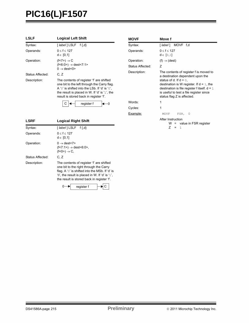
PIC16(L)F1507
LSLF Logical Left Shift
Syntax: [ label ] LSLF f {,d}
Operands: 0 f 127d [0,1]
Operation: (f<7>) C(f<6:0>) dest<7:1>0 dest<0>
Status Affected: C, Z
Description: The contents of register ‘f’ are shifted one bit to the left through the Carry flag. A ‘0’ is shifted into the LSb. If ‘d’ is ‘0’, the result is placed in W. If ‘d’ is ‘1’, the result is stored back in register ‘f’.
LSRF Logical Right Shift
Syntax: [ label ] LSLF f {,d}
Operands: 0 f 127d [0,1]
Operation: 0 dest<7>(f<7:1>) dest<6:0>,(f<0>) C,
Status Affected: C, Z
Description: The contents of register ‘f’ are shifted one bit to the right through the Carry flag. A ‘0’ is shifted into the MSb. If ‘d’ is ‘0’, the result is placed in W. If ‘d’ is ‘1’, the result is stored back in register ‘f’.
register f 0C
register f C0
MOVF Move f
Syntax: [ label ] MOVF f,d
Operands: 0 f 127d [0,1]
Operation: (f) (dest)
Status Affected: Z
Description: The contents of register f is moved to a destination dependent upon the status of d. If d = 0,destination is W register. If d = 1, the destination is file register f itself. d = 1 is useful to test a file register since status flag Z is affected.
Words: 1
Cycles: 1
Example: MOVF FSR, 0
After InstructionW = value in FSR registerZ = 1
DS41586A-page 215 Preliminary 2011 Microchip Technology Inc.
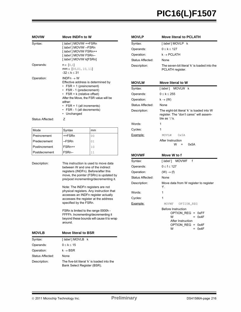
PIC16(L)F1507
MOVIW Move INDFn to W
Syntax: [ label ] MOVIW ++FSRn[ label ] MOVIW --FSRn[ label ] MOVIW FSRn++[ label ] MOVIW FSRn--[ label ] MOVIW k[FSRn]
Operands: n [0,1]mm [00,01, 10, 11]-32 k 31
Operation: INDFn WEffective address is determined by• FSR + 1 (preincrement)• FSR - 1 (predecrement)• FSR + k (relative offset)After the Move, the FSR value will be either:• FSR + 1 (all increments)• FSR - 1 (all decrements)• Unchanged
Status Affected: Z
Mode Syntax mm
Preincrement ++FSRn 00
Predecrement --FSRn 01
Postincrement FSRn++ 10
Postdecrement FSRn-- 11
Description: This instruction is used to move data between W and one of the indirect registers (INDFn). Before/after this move, the pointer (FSRn) is updated by pre/post incrementing/decrementing it.
Note: The INDFn registers are not physical registers. Any instruction that accesses an INDFn register actually accesses the register at the address specified by the FSRn.
FSRn is limited to the range 0000h - FFFFh. Incrementing/decrementing it beyond these bounds will cause it to wrap around.
MOVLB Move literal to BSR
Syntax: [ label ] MOVLB k
Operands: 0 k 15
Operation: k BSR
Status Affected: None
Description: The five-bit literal ‘k’ is loaded into the Bank Select Register (BSR).
MOVLP Move literal to PCLATH
Syntax: [ label ] MOVLP k
Operands: 0 k 127
Operation: k PCLATH
Status Affected: None
Description: The seven-bit literal ‘k’ is loaded into the PCLATH register.
MOVLW Move literal to W
Syntax: [ label ] MOVLW k
Operands: 0 k 255
Operation: k (W)
Status Affected: None
Description: The eight-bit literal ‘k’ is loaded into W register. The “don’t cares” will assem-ble as ‘0’s.
Words: 1
Cycles: 1
Example: MOVLW 0x5A
After InstructionW = 0x5A
MOVWF Move W to f
Syntax: [ label ] MOVWF f
Operands: 0 f 127
Operation: (W) (f)
Status Affected: None
Description: Move data from W register to register ‘f’.
Words: 1
Cycles: 1
Example: MOVWF OPTION_REG
Before InstructionOPTION_REG = 0xFFW = 0x4FAfter InstructionOPTION_REG = 0x4FW = 0x4F
2011 Microchip Technology Inc. Preliminary DS41586A-page 216
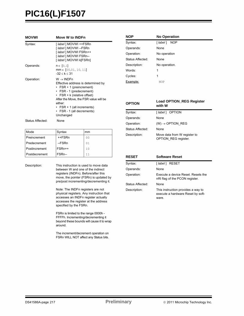
PIC16(L)F1507
MOVWI Move W to INDFn
Syntax: [ label ] MOVWI ++FSRn[ label ] MOVWI --FSRn[ label ] MOVWI FSRn++[ label ] MOVWI FSRn--[ label ] MOVWI k[FSRn]
Operands: n [0,1]mm [00,01, 10, 11]-32 k 31
Operation: W INDFnEffective address is determined by• FSR + 1 (preincrement)• FSR - 1 (predecrement)• FSR + k (relative offset)After the Move, the FSR value will be either:• FSR + 1 (all increments)• FSR - 1 (all decrements)Unchanged
Status Affected: None
Mode Syntax mm
Preincrement ++FSRn 00
Predecrement --FSRn 01
Postincrement FSRn++ 10
Postdecrement FSRn-- 11
Description: This instruction is used to move data between W and one of the indirect registers (INDFn). Before/after this move, the pointer (FSRn) is updated by pre/post incrementing/decrementing it.
Note: The INDFn registers are not physical registers. Any instruction that accesses an INDFn register actually accesses the register at the address specified by the FSRn.
FSRn is limited to the range 0000h - FFFFh. Incrementing/decrementing it beyond these bounds will cause it to wrap around.
The increment/decrement operation on FSRn WILL NOT affect any Status bits.
NOP No Operation
Syntax: [ label ] NOP
Operands: None
Operation: No operation
Status Affected: None
Description: No operation.
Words: 1
Cycles: 1
Example: NOP
OPTIONLoad OPTION_REG Register with W
Syntax: [ label ] OPTION
Operands: None
Operation: (W) OPTION_REG
Status Affected: None
Description: Move data from W register to OPTION_REG register.
RESET Software Reset
Syntax: [ label ] RESET
Operands: None
Operation: Execute a device Reset. Resets the nRI flag of the PCON register.
Status Affected: None
Description: This instruction provides a way to execute a hardware Reset by soft-ware.
DS41586A-page 217 Preliminary 2011 Microchip Technology Inc.
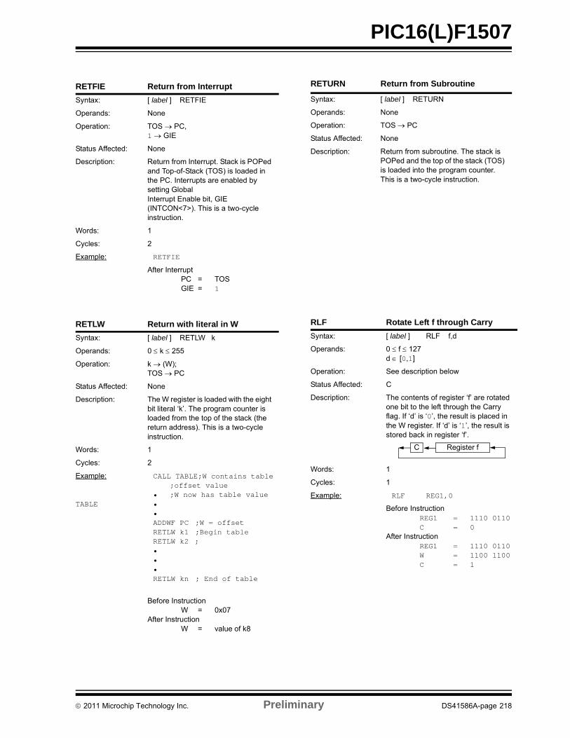
PIC16(L)F1507
RETFIE Return from Interrupt
Syntax: [ label ] RETFIE
Operands: None
Operation: TOS PC,1 GIE
Status Affected: None
Description: Return from Interrupt. Stack is POPed and Top-of-Stack (TOS) is loaded in the PC. Interrupts are enabled by setting GlobalInterrupt Enable bit, GIE (INTCON<7>). This is a two-cycle instruction.
Words: 1
Cycles: 2
Example: RETFIE
After InterruptPC = TOSGIE = 1
RETLW Return with literal in W
Syntax: [ label ] RETLW k
Operands: 0 k 255
Operation: k (W); TOS PC
Status Affected: None
Description: The W register is loaded with the eight bit literal ‘k’. The program counter is loaded from the top of the stack (the return address). This is a two-cycle instruction.
Words: 1
Cycles: 2
Example:
TABLE
CALL TABLE;W contains table;offset value
• ;W now has table value••ADDWF PC ;W = offsetRETLW k1 ;Begin tableRETLW k2 ;•••RETLW kn ; End of table
Before InstructionW = 0x07
After InstructionW = value of k8
RETURN Return from Subroutine
Syntax: [ label ] RETURN
Operands: None
Operation: TOS PC
Status Affected: None
Description: Return from subroutine. The stack is POPed and the top of the stack (TOS) is loaded into the program counter. This is a two-cycle instruction.
RLF Rotate Left f through Carry
Syntax: [ label ] RLF f,d
Operands: 0 f 127d [0,1]
Operation: See description below
Status Affected: C
Description: The contents of register ‘f’ are rotated one bit to the left through the Carry flag. If ‘d’ is ‘0’, the result is placed in the W register. If ‘d’ is ‘1’, the result is stored back in register ‘f’.
Words: 1
Cycles: 1
Example: RLF REG1,0
Before InstructionREG1 = 1110 0110C = 0
After InstructionREG1 = 1110 0110W = 1100 1100C = 1
Register fC
2011 Microchip Technology Inc. Preliminary DS41586A-page 218
PIC16(L)F1507
RRF Rotate Right f through Carry
Syntax: [ label ] RRF f,d
Operands: 0 f 127d [0,1]
Operation: See description below
Status Affected: C
Description: The contents of register ‘f’ are rotated one bit to the right through the Carry flag. If ‘d’ is ‘0’, the result is placed in the W register. If ‘d’ is ‘1’, the result is placed back in register ‘f’.
SLEEP Enter Sleep mode
Syntax: [ label ] SLEEP
Operands: None
Operation: 00h WDT,0 WDT prescaler,1 TO,0 PD
Status Affected: TO, PD
Description: The power-down Status bit, PD is cleared. Time-out Status bit, TO is set. Watchdog Timer and its pres-caler are cleared.The processor is put into Sleep mode with the oscillator stopped.
Register fC
SUBLW Subtract W from literal
Syntax: [ label ] SUBLW k
Operands: 0 k 255
Operation: k - (W) W)
Status Affected: C, DC, Z
Description: The W register is subtracted (2’s com-plement method) from the eight-bit literal ‘k’. The result is placed in the W register.
SUBWF Subtract W from f
Syntax: [ label ] SUBWF f,d
Operands: 0 f 127d [0,1]
Operation: (f) - (W) destination)
Status Affected: C, DC, Z
Description: Subtract (2’s complement method) W register from register ‘f’. If ‘d’ is ‘0’, the result is stored in the W register. If ‘d’ is ‘1’, the result is stored back in register ‘f.
SUBWFB Subtract W from f with Borrow
Syntax: SUBWFB f {,d}
Operands: 0 f 127d [0,1]
Operation: (f) – (W) – (B) dest
Status Affected: C, DC, Z
Description: Subtract W and the BORROW flag (CARRY) from register ‘f’ (2’s comple-ment method). If ‘d’ is ‘0’, the result is stored in W. If ‘d’ is ‘1’, the result is stored back in register ‘f’.
C = 0 W k
C = 1 W k
DC = 0 W<3:0> k<3:0>
DC = 1 W<3:0> k<3:0>
C = 0 W f
C = 1 W f
DC = 0 W<3:0> f<3:0>
DC = 1 W<3:0> f<3:0>
DS41586A-page 219 Preliminary 2011 Microchip Technology Inc.
PIC16(L)F1507
SWAPF Swap Nibbles in f
Syntax: [ label ] SWAPF f,d
Operands: 0 f 127d [0,1]
Operation: (f<3:0>) (destination<7:4>),(f<7:4>) (destination<3:0>)
Status Affected: None
Description: The upper and lower nibbles of regis-ter ‘f’ are exchanged. If ‘d’ is ‘0’, the result is placed in the W register. If ‘d’ is ‘1’, the result is placed in register ‘f’.
TRIS Load TRIS Register with W
Syntax: [ label ] TRIS f
Operands: 5 f 7
Operation: (W) TRIS register ‘f’
Status Affected: None
Description: Move data from W register to TRIS register.When ‘f’ = 5, TRISA is loaded.When ‘f’ = 6, TRISB is loaded.When ‘f’ = 7, TRISC is loaded.
XORLW Exclusive OR literal with W
Syntax: [ label ] XORLW k
Operands: 0 k 255
Operation: (W) .XOR. k W)
Status Affected: Z
Description: The contents of the W register are XOR’ed with the eight-bitliteral ‘k’. The result is placed in the W register.
XORWF Exclusive OR W with f
Syntax: [ label ] XORWF f,d
Operands: 0 f 127d [0,1]
Operation: (W) .XOR. (f) destination)
Status Affected: Z
Description: Exclusive OR the contents of the W register with register ‘f’. If ‘d’ is ‘0’, the result is stored in the W register. If ‘d’ is ‘1’, the result is stored back in regis-ter ‘f’.
2011 Microchip Technology Inc. Preliminary DS41586A-page 220
PIC16(L)F1507
25.0 ELECTRICAL SPECIFICATIONS
Absolute Maximum Ratings(†)
Ambient temperature under bias ....................................................................................................... -40°C to +125°C
Storage temperature ........................................................................................................................ -65°C to +150°C
Voltage on VDD with respect to VSS, PIC16F1507 ............................................................................. -0.3V to +6.5V
Voltage on VDD with respect to VSS, PIC16LF1507 ........................................................................... -0.3V to +4.0V
Voltage on MCLR with respect to Vss ................................................................................................. -0.3V to +9.0V
Voltage on all other pins with respect to VSS ............................................................................ -0.3V to (VDD + 0.3V)
Total power dissipation(1) ...............................................................................................................................800 mW
Maximum current out of VSS pin, -40°C TA +85°C for industrial ............................................................... 396 mA
Maximum current out of VSS pin, -40°C TA +125°C for extended ............................................................ 114 mA
Maximum current into VDD pin, -40°C TA +85°C for industrial.................................................................. 292 mA
Maximum current into VDD pin, -40°C TA +125°C for extended ............................................................... 107 mA
Clamp current, IK (VPIN < 0 or VPIN > VDD)20 mA
Maximum output current sunk by any I/O pin....................................................................................................25 mA
Maximum output current sourced by any I/O pin...............................................................................................25 mA
Note 1: Power dissipation is calculated as follows: PDIS = VDD x {IDD – IOH} + {(VDD – VOH) x IOH} + (VOl x IOL).
† NOTICE: Stresses above those listed under “Absolute Maximum Ratings” may cause permanent damage to the device. This is a stress rating only and functional operation of the device at those or any other conditions above those indicated in the operation listings of this specification is not implied. Exposure above maximum rating conditions for extended periods may affect device reliability.
DS41586A-page 221 Preliminary 2011 Microchip Technology Inc.
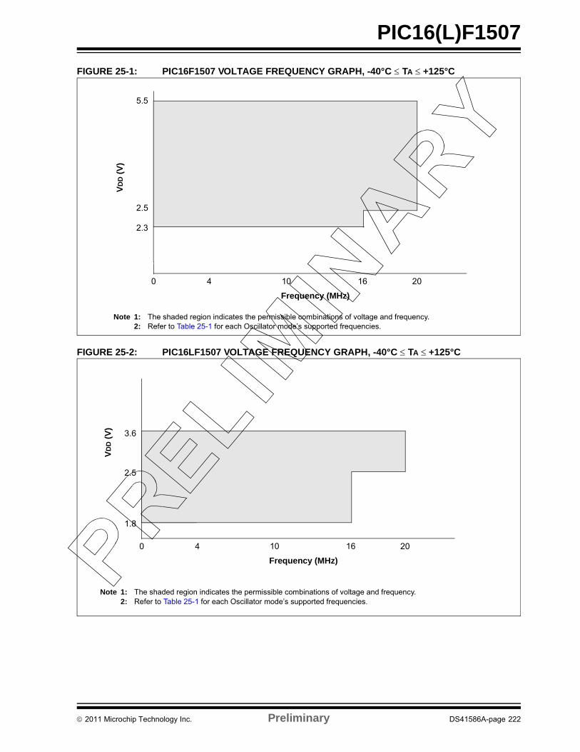
PIC16(L)F1507
FIGURE 25-1: PIC16F1507 VOLTAGE FREQUENCY GRAPH, -40°C TA +125°C
FIGURE 25-2: PIC16LF1507 VOLTAGE FREQUENCY GRAPH, -40°C TA +125°C
Note 1: The shaded region indicates the permissible combinations of voltage and frequency.2: Refer to Table 25-1 for each Oscillator mode’s supported frequencies.
2.3
0
2.5
Frequency (MHz)
VD
D (
V)
4 2010 16
5.5
Note 1: The shaded region indicates the permissible combinations of voltage and frequency.2: Refer to Table 25-1 for each Oscillator mode’s supported frequencies.
1.8
0
2.5
Frequency (MHz)
VD
D (
V)
4 2010 16
3.6
2011 Microchip Technology Inc. Preliminary DS41586A-page 222
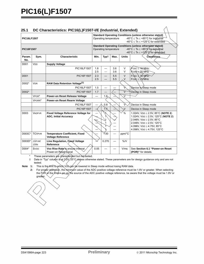
PIC16(L)F1507
25.1 DC Characteristics: PIC16(L)F1507-I/E (Industrial, Extended)
PIC16LF1507Standard Operating Conditions (unless otherwise stated)Operating temperature -40°C TA +85°C for industrial
-40°C TA +125°C for extended
PIC16F1507Standard Operating Conditions (unless otherwise stated)Operating temperature -40°C TA +85°C for industrial
-40°C TA +125°C for extended
Param. No.
Sym. Characteristic Min. Typ† Max. Units Conditions
D001 VDD Supply Voltage
PIC16LF1507 1.82.5
——
3.63.6
VV
FOSC 16 MHz:FOSC 20 MHz
D001 PIC16F1507 2.32.5
——
5.55.5
VV
FOSC 16 MHz:FOSC 20 MHz
D002* VDR RAM Data Retention Voltage(1)
PIC16LF1507 1.5 — — V Device in Sleep mode
D002* PIC16F1507 1.7 — — V Device in Sleep mode
VPOR* Power-on Reset Release Voltage — 1.6 — V
VPORR* Power-on Reset Rearm Voltage
PIC16LF1507 — 0.8 — V Device in Sleep mode
PIC16F1507 — 1.7 — V Device in Sleep mode
D003 VADFVR Fixed Voltage Reference Voltage for ADC, Initial Accuracy
——————
111111
——————
% 1.024V, VDD 2.5V, 85°C (NOTE 2)1.024V, VDD 2.5V, 125°C (NOTE 2)2.048V, VDD 2.5V, 85°C2.048V, VDD 2.5V, 125°C4.096V, VDD 4.75V, 85°C4.096V, VDD 4.75V, 125°C
D003C* TCVFVR Temperature Coefficient, Fixed Voltage Reference
— -130 — ppm/°C
D003D* VFVR/VIN
Line Regulation, Fixed Voltage Reference
— 0.270 — %/V
D004* SVDD VDD Rise Rate to ensure internal Power-on Reset signal
0.05 — — V/ms See Section 6.1 “Power-on Reset (POR)” for details.
* These parameters are characterized but not tested.† Data in “Typ” column is at 3.0V, 25°C unless otherwise stated. These parameters are for design guidance only and are not
tested.Note 1: This is the limit to which VDD can be lowered in Sleep mode without losing RAM data.
2: For proper operation, the minimum value of the ADC positive voltage reference must be 1.8V or greater. When selecting the FVR or the VREF+ pin as the source of the ADC positive voltage reference, be aware that the voltage must be 1.8V or greater.
DS41586A-page 223 Preliminary 2011 Microchip Technology Inc.
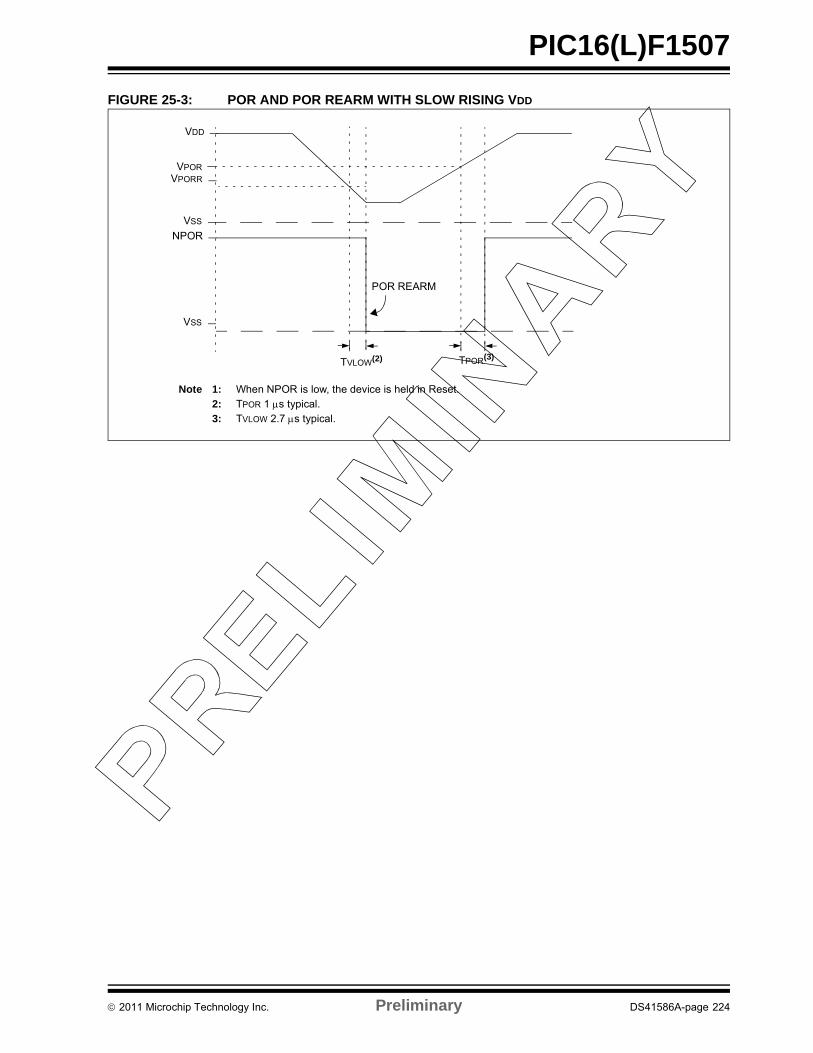
PIC16(L)F1507
FIGURE 25-3: POR AND POR REARM WITH SLOW RISING VDD
VDD
VPOR
VPORR
VSS
VSS
NPOR
TPOR(3)
POR REARM
Note 1: When NPOR is low, the device is held in Reset.2: TPOR 1 s typical.3: TVLOW 2.7 s typical.
TVLOW(2)
2011 Microchip Technology Inc. Preliminary DS41586A-page 224
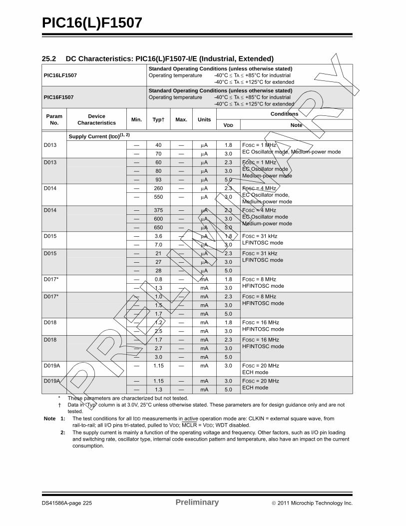
PIC16(L)F1507
25.2 DC Characteristics: PIC16(L)F1507-I/E (Industrial, Extended)
PIC16LF1507Standard Operating Conditions (unless otherwise stated)Operating temperature -40°C TA +85°C for industrial
-40°C TA +125°C for extended
PIC16F1507Standard Operating Conditions (unless otherwise stated)Operating temperature -40°C TA +85°C for industrial
-40°C TA +125°C for extended
ParamNo.
Device Characteristics
Min. Typ† Max. UnitsConditions
VDD Note
Supply Current (IDD)(1, 2)
D013 — 40 — A 1.8 FOSC = 1 MHzEC Oscillator mode, Medium-power mode— 70 — A 3.0
D013 — 60 — A 2.3 FOSC = 1 MHzEC Oscillator modeMedium-power mode
— 80 — A 3.0
— 93 — A 5.0
D014 — 260 — A 2.3 FOSC = 4 MHzEC Oscillator mode,Medium-power mode
— 550 — A 3.0
D014 — 375 — A 2.3 FOSC = 4 MHzEC Oscillator mode Medium-power mode
— 600 — A 3.0
— 650 — A 5.0
D015 — 3.6 — A 1.8 FOSC = 31 kHzLFINTOSC mode— 7.0 — A 3.0
D015 — 21 — A 2.3 FOSC = 31 kHzLFINTOSC mode — 27 — A 3.0
— 28 — A 5.0
D017* — 0.8 — mA 1.8 FOSC = 8 MHzHFINTOSC mode— 1.3 — mA 3.0
D017* — 1.0 — mA 2.3 FOSC = 8 MHzHFINTOSC mode — 1.5 — mA 3.0
— 1.7 — mA 5.0
D018 — 1.2 — mA 1.8 FOSC = 16 MHzHFINTOSC mode— 2.5 — mA 3.0
D018 — 1.7 — mA 2.3 FOSC = 16 MHzHFINTOSC mode — 2.7 — mA 3.0
— 3.0 — mA 5.0
D019A — 1.15 — mA 3.0 FOSC = 20 MHzECH mode
D019A — 1.15 — mA 3.0 FOSC = 20 MHzECH mode— 1.3 — mA 5.0
* These parameters are characterized but not tested.† Data in “Typ” column is at 3.0V, 25°C unless otherwise stated. These parameters are for design guidance only and are not
tested.
Note 1: The test conditions for all IDD measurements in active operation mode are: CLKIN = external square wave, from rail-to-rail; all I/O pins tri-stated, pulled to VDD; MCLR = VDD; WDT disabled.
2: The supply current is mainly a function of the operating voltage and frequency. Other factors, such as I/O pin loading and switching rate, oscillator type, internal code execution pattern and temperature, also have an impact on the current consumption.
DS41586A-page 225 Preliminary 2011 Microchip Technology Inc.
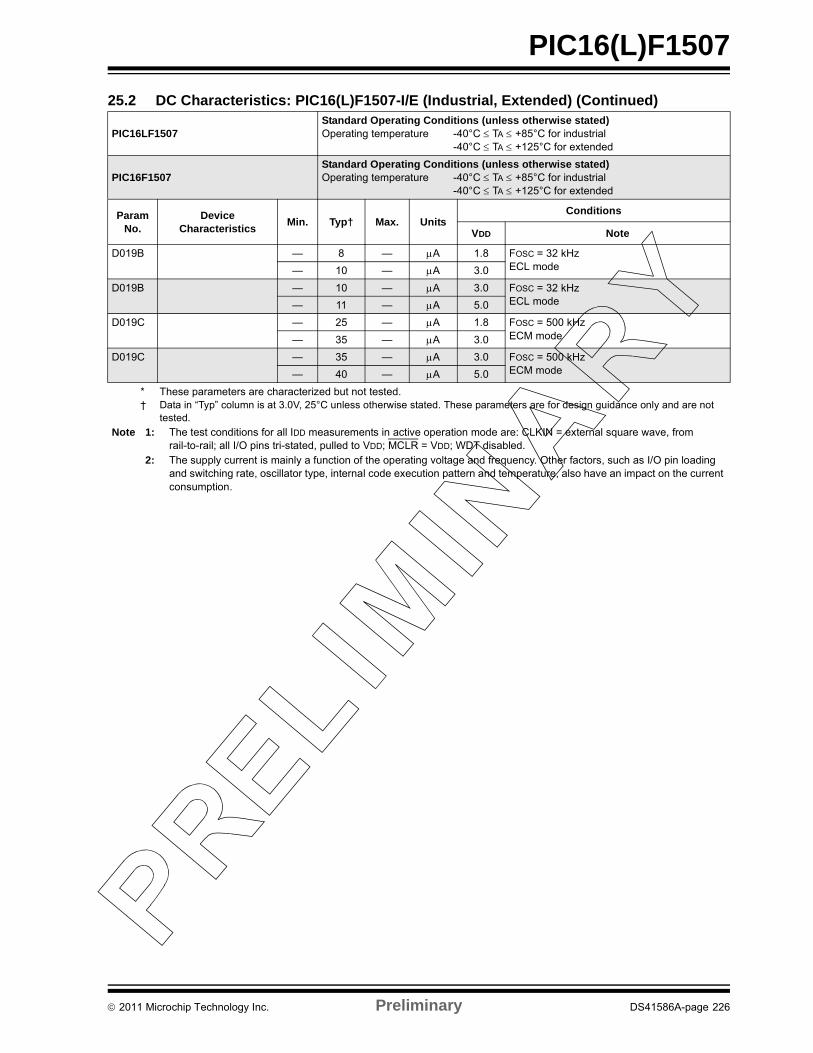
PIC16(L)F1507
D019B — 8 — A 1.8 FOSC = 32 kHzECL mode— 10 — A 3.0
D019B — 10 — A 3.0 FOSC = 32 kHzECL mode— 11 — A 5.0
D019C — 25 — A 1.8 FOSC = 500 kHzECM mode— 35 — A 3.0
D019C — 35 — A 3.0 FOSC = 500 kHzECM mode— 40 — A 5.0
25.2 DC Characteristics: PIC16(L)F1507-I/E (Industrial, Extended) (Continued)
PIC16LF1507Standard Operating Conditions (unless otherwise stated)Operating temperature -40°C TA +85°C for industrial
-40°C TA +125°C for extended
PIC16F1507Standard Operating Conditions (unless otherwise stated)Operating temperature -40°C TA +85°C for industrial
-40°C TA +125°C for extended
ParamNo.
Device Characteristics
Min. Typ† Max. UnitsConditions
VDD Note
* These parameters are characterized but not tested.† Data in “Typ” column is at 3.0V, 25°C unless otherwise stated. These parameters are for design guidance only and are not
tested.
Note 1: The test conditions for all IDD measurements in active operation mode are: CLKIN = external square wave, from rail-to-rail; all I/O pins tri-stated, pulled to VDD; MCLR = VDD; WDT disabled.
2: The supply current is mainly a function of the operating voltage and frequency. Other factors, such as I/O pin loading and switching rate, oscillator type, internal code execution pattern and temperature, also have an impact on the current consumption.
2011 Microchip Technology Inc. Preliminary DS41586A-page 226
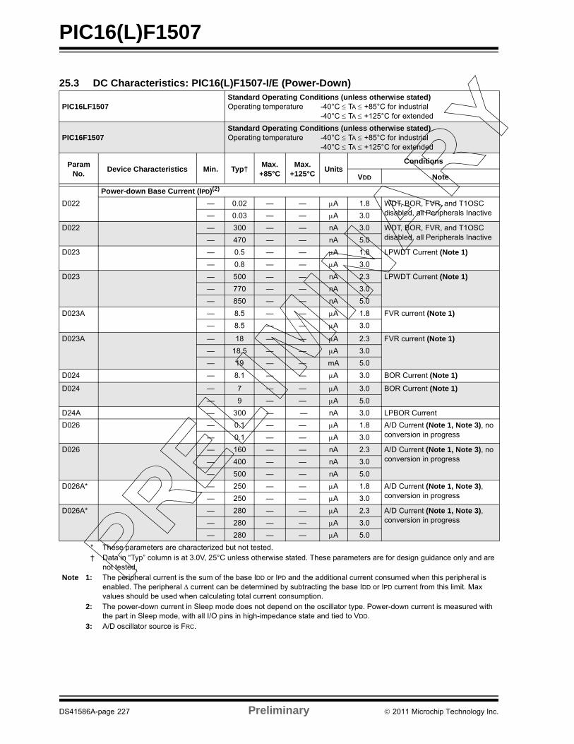
PIC16(L)F1507
25.3 DC Characteristics: PIC16(L)F1507-I/E (Power-Down)
PIC16LF1507Standard Operating Conditions (unless otherwise stated)Operating temperature -40°C TA +85°C for industrial
-40°C TA +125°C for extended
PIC16F1507Standard Operating Conditions (unless otherwise stated)Operating temperature -40°C TA +85°C for industrial
-40°C TA +125°C for extended
ParamNo.
Device Characteristics Min. Typ†Max.
+85°CMax.
+125°CUnits
Conditions
VDD Note
Power-down Base Current (IPD)(2)
D022 — 0.02 — — A 1.8 WDT, BOR, FVR, and T1OSC disabled, all Peripherals Inactive— 0.03 — — A 3.0
D022 — 300 — — nA 3.0 WDT, BOR, FVR, and T1OSC disabled, all Peripherals Inactive— 470 — — nA 5.0
D023 — 0.5 — — A 1.8 LPWDT Current (Note 1)
— 0.8 — — A 3.0
D023 — 500 — — nA 2.3 LPWDT Current (Note 1)
— 770 — — nA 3.0
— 850 — — nA 5.0
D023A — 8.5 — — A 1.8 FVR current (Note 1)
— 8.5 — — A 3.0
D023A — 18 — — A 2.3 FVR current (Note 1)
— 18.5 — — A 3.0
— 19 — — mA 5.0
D024 — 8.1 — — A 3.0 BOR Current (Note 1)
D024 — 7 — — A 3.0 BOR Current (Note 1)
— 9 — — A 5.0
D24A — 300 — — nA 3.0 LPBOR Current
D026 — 0.1 — — A 1.8 A/D Current (Note 1, Note 3), no conversion in progress— 0.1 — — A 3.0
D026 — 160 — — nA 2.3 A/D Current (Note 1, Note 3), no conversion in progress— 400 — — nA 3.0
— 500 — — nA 5.0
D026A* — 250 — — A 1.8 A/D Current (Note 1, Note 3), conversion in progress— 250 — — A 3.0
D026A* — 280 — — A 2.3 A/D Current (Note 1, Note 3), conversion in progress— 280 — — A 3.0
— 280 — — A 5.0
* These parameters are characterized but not tested.† Data in “Typ” column is at 3.0V, 25°C unless otherwise stated. These parameters are for design guidance only and are
not tested.Note 1: The peripheral current is the sum of the base IDD or IPD and the additional current consumed when this peripheral is
enabled. The peripheral current can be determined by subtracting the base IDD or IPD current from this limit. Max values should be used when calculating total current consumption.
2: The power-down current in Sleep mode does not depend on the oscillator type. Power-down current is measured with the part in Sleep mode, with all I/O pins in high-impedance state and tied to VDD.
3: A/D oscillator source is FRC.
DS41586A-page 227 Preliminary 2011 Microchip Technology Inc.
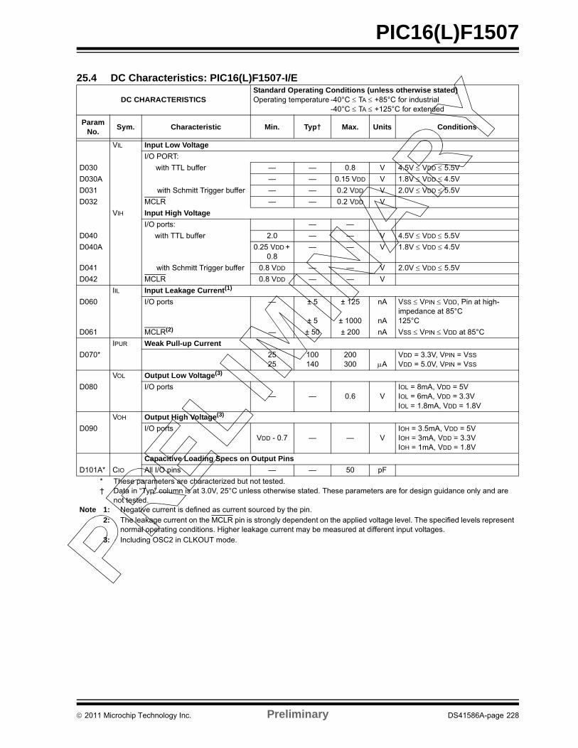
PIC16(L)F1507
25.4 DC Characteristics: PIC16(L)F1507-I/E
DC CHARACTERISTICSStandard Operating Conditions (unless otherwise stated)Operating temperature -40°C TA +85°C for industrial
-40°C TA +125°C for extended
ParamNo.
Sym. Characteristic Min. Typ† Max. Units Conditions
VIL Input Low Voltage
I/O PORT:
D030 with TTL buffer — — 0.8 V 4.5V VDD 5.5V
D030A — — 0.15 VDD V 1.8V VDD 4.5V
D031 with Schmitt Trigger buffer — — 0.2 VDD V 2.0V VDD 5.5V
D032 MCLR — — 0.2 VDD V
VIH Input High Voltage
I/O ports: — —
D040 with TTL buffer 2.0 — — V 4.5V VDD 5.5V
D040A 0.25 VDD + 0.8
— — V 1.8V VDD 4.5V
D041 with Schmitt Trigger buffer 0.8 VDD — — V 2.0V VDD 5.5V
D042 MCLR 0.8 VDD — — V
IIL Input Leakage Current(1)
D060 I/O ports — ± 5
± 5
± 125
± 1000
nA
nA
VSS VPIN VDD, Pin at high-impedance at 85°C125°C
D061 MCLR(2) — ± 50 ± 200 nA VSS VPIN VDD at 85°C
IPUR Weak Pull-up Current
D070* 2525
100140
200300 A
VDD = 3.3V, VPIN = VSS
VDD = 5.0V, VPIN = VSS
VOL Output Low Voltage(3)
D080 I/O ports— — 0.6 V
IOL = 8mA, VDD = 5VIOL = 6mA, VDD = 3.3VIOL = 1.8mA, VDD = 1.8V
VOH Output High Voltage(3)
D090 I/O portsVDD - 0.7 — — V
IOH = 3.5mA, VDD = 5VIOH = 3mA, VDD = 3.3VIOH = 1mA, VDD = 1.8V
Capacitive Loading Specs on Output Pins
D101A* CIO All I/O pins — — 50 pF
* These parameters are characterized but not tested.† Data in “Typ” column is at 3.0V, 25°C unless otherwise stated. These parameters are for design guidance only and are
not tested.Note 1: Negative current is defined as current sourced by the pin.
2: The leakage current on the MCLR pin is strongly dependent on the applied voltage level. The specified levels represent normal operating conditions. Higher leakage current may be measured at different input voltages.
3: Including OSC2 in CLKOUT mode.
2011 Microchip Technology Inc. Preliminary DS41586A-page 228
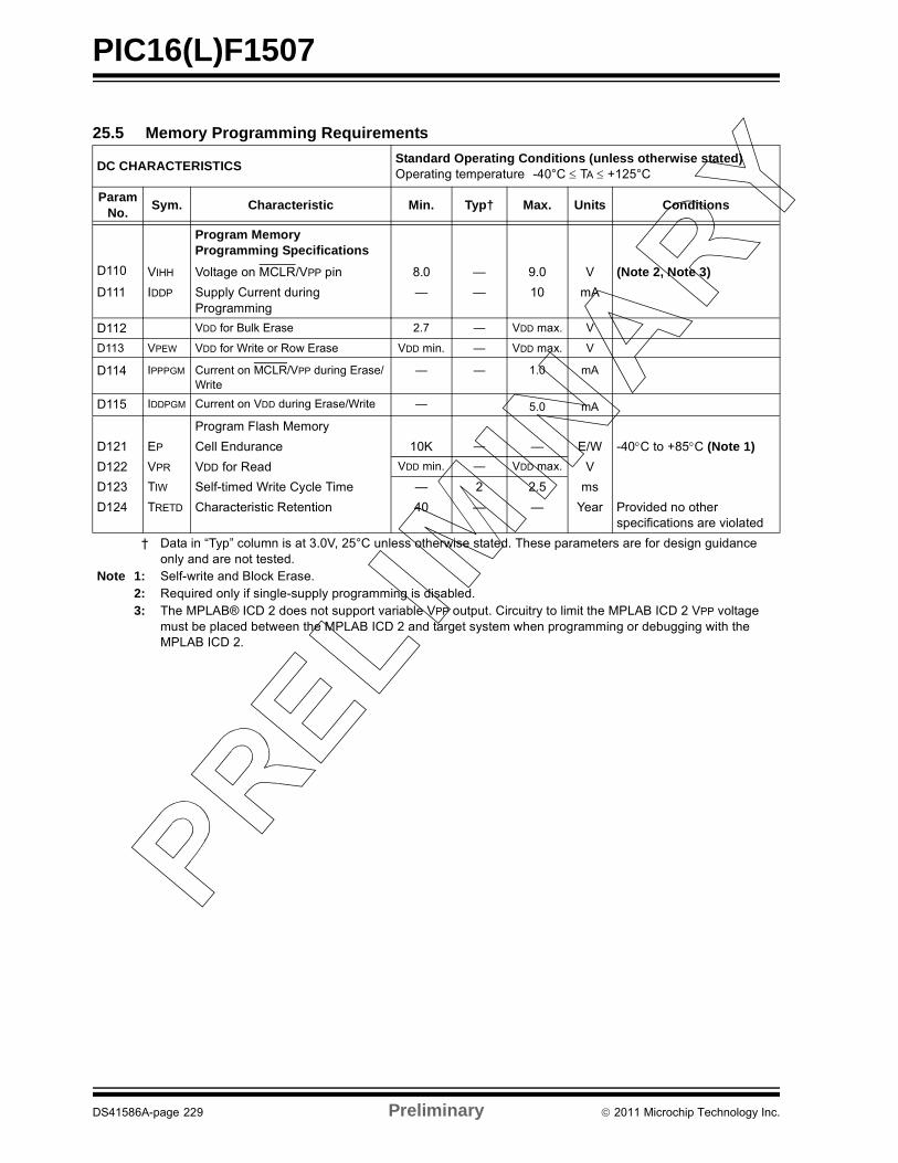
PIC16(L)F1507
25.5 Memory Programming Requirements
DC CHARACTERISTICSStandard Operating Conditions (unless otherwise stated)Operating temperature -40°C TA +125°C
ParamNo.
Sym. Characteristic Min. Typ† Max. Units Conditions
Program Memory Programming Specifications
D110 VIHH Voltage on MCLR/VPP pin 8.0 — 9.0 V (Note 2, Note 3)
D111 IDDP Supply Current during Programming
— — 10 mA
D112 VDD for Bulk Erase 2.7 — VDD max. V
D113 VPEW VDD for Write or Row Erase VDD min. — VDD max. V
D114 IPPPGM Current on MCLR/VPP during Erase/Write
— — 1.0 mA
D115 IDDPGM Current on VDD during Erase/Write — 5.0 mA
Program Flash Memory
D121 EP Cell Endurance 10K — — E/W -40C to +85C (Note 1)
D122 VPR VDD for Read VDD min. — VDD max. V
D123 TIW Self-timed Write Cycle Time — 2 2.5 ms
D124 TRETD Characteristic Retention 40 — — Year Provided no other specifications are violated
† Data in “Typ” column is at 3.0V, 25°C unless otherwise stated. These parameters are for design guidance only and are not tested.
Note 1: Self-write and Block Erase.2: Required only if single-supply programming is disabled.3: The MPLAB® ICD 2 does not support variable VPP output. Circuitry to limit the MPLAB ICD 2 VPP voltage
must be placed between the MPLAB ICD 2 and target system when programming or debugging with the MPLAB ICD 2.
DS41586A-page 229 Preliminary 2011 Microchip Technology Inc.
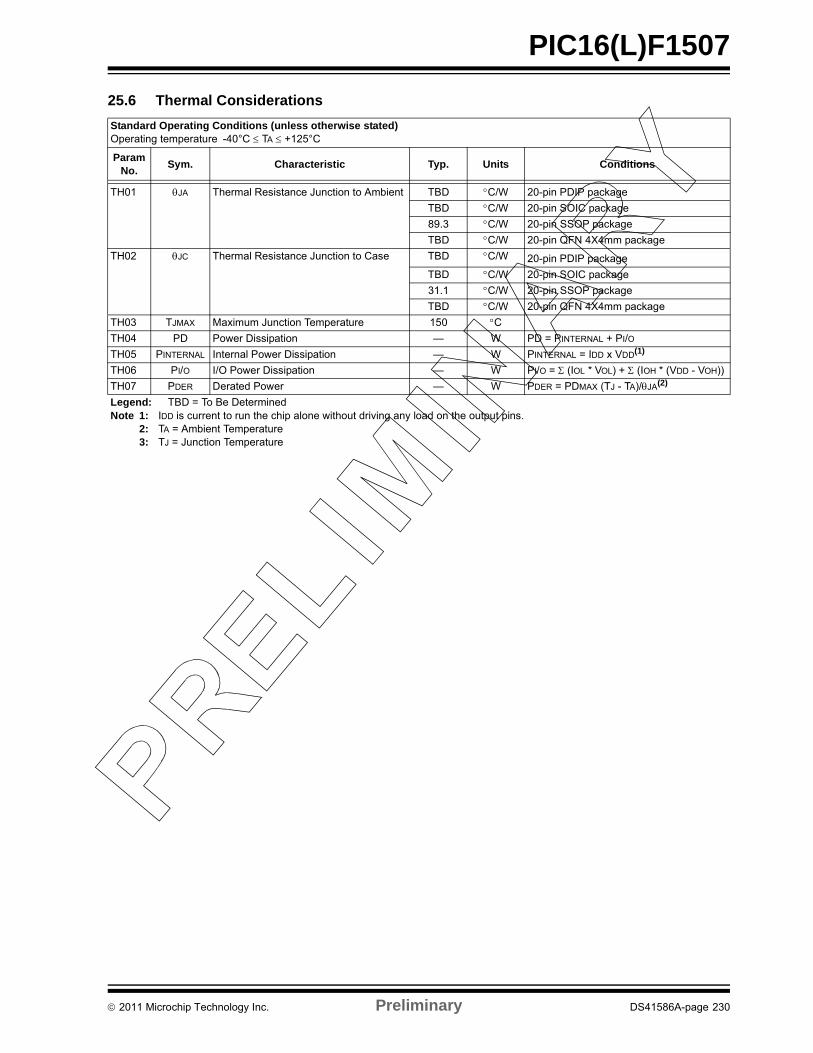
PIC16(L)F1507
25.6 Thermal Considerations
Standard Operating Conditions (unless otherwise stated)Operating temperature -40°C TA +125°C
ParamNo.
Sym. Characteristic Typ. Units Conditions
TH01 JA Thermal Resistance Junction to Ambient TBD C/W 20-pin PDIP package
TBD C/W 20-pin SOIC package
89.3 C/W 20-pin SSOP package
TBD C/W 20-pin QFN 4X4mm package
TH02 JC Thermal Resistance Junction to Case TBD C/W 20-pin PDIP package
TBD C/W 20-pin SOIC package
31.1 C/W 20-pin SSOP package
TBD C/W 20-pin QFN 4X4mm package
TH03 TJMAX Maximum Junction Temperature 150 CTH04 PD Power Dissipation — W PD = PINTERNAL + PI/O
TH05 PINTERNAL Internal Power Dissipation — W PINTERNAL = IDD x VDD(1)
TH06 PI/O I/O Power Dissipation — W PI/O = (IOL * VOL) + (IOH * (VDD - VOH))
TH07 PDER Derated Power — W PDER = PDMAX (TJ - TA)/JA(2)
Legend: TBD = To Be DeterminedNote 1: IDD is current to run the chip alone without driving any load on the output pins.
2: TA = Ambient Temperature3: TJ = Junction Temperature
2011 Microchip Technology Inc. Preliminary DS41586A-page 230
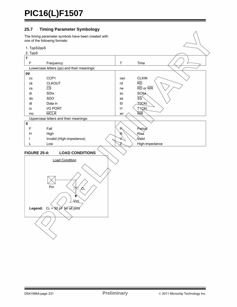
PIC16(L)F1507
25.7 Timing Parameter Symbology
The timing parameter symbols have been created withone of the following formats:
FIGURE 25-4: LOAD CONDITIONS
1. TppS2ppS
2. TppS
T
F Frequency T Time
Lowercase letters (pp) and their meanings:
pp
cc CCP1 osc CLKIN
ck CLKOUT rd RD
cs CS rw RD or WR
di SDIx sc SCKx
do SDO ss SS
dt Data in t0 T0CKI
io I/O PORT t1 T1CKI
mc MCLR wr WR
Uppercase letters and their meanings:
S
F Fall P Period
H High R Rise
I Invalid (High-impedance) V Valid
L Low Z High-impedance
VSS
CL
Legend: CL = 50 pF for all pins
Load Condition
Pin
DS41586A-page 231 Preliminary 2011 Microchip Technology Inc.
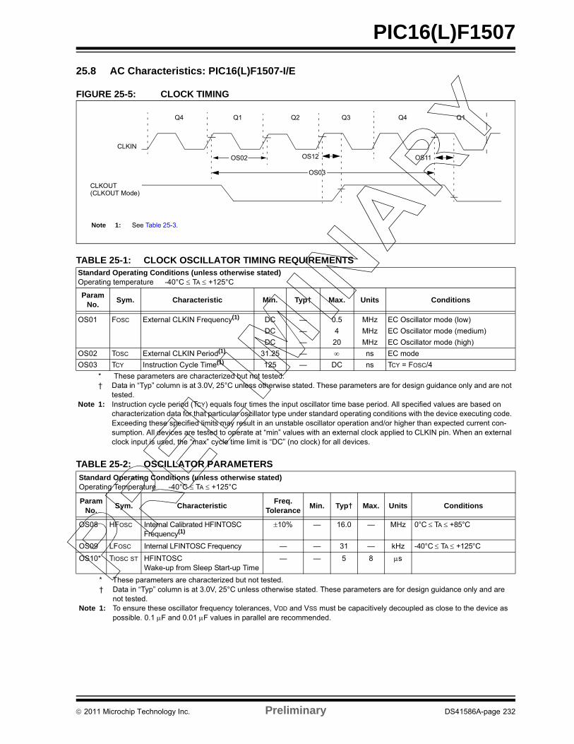
PIC16(L)F1507
25.8 AC Characteristics: PIC16(L)F1507-I/E
FIGURE 25-5: CLOCK TIMING
TABLE 25-1: CLOCK OSCILLATOR TIMING REQUIREMENTS
TABLE 25-2: OSCILLATOR PARAMETERS
Standard Operating Conditions (unless otherwise stated)Operating temperature -40°C TA +125°C
ParamNo.
Sym. Characteristic Min. Typ† Max. Units Conditions
OS01 FOSC External CLKIN Frequency(1) DC — 0.5 MHz EC Oscillator mode (low)
DC — 4 MHz EC Oscillator mode (medium)
DC — 20 MHz EC Oscillator mode (high)
OS02 TOSC External CLKIN Period(1) 31.25 — ns EC mode
OS03 TCY Instruction Cycle Time(1) 125 — DC ns TCY = FOSC/4
* These parameters are characterized but not tested.† Data in “Typ” column is at 3.0V, 25°C unless otherwise stated. These parameters are for design guidance only and are not
tested.Note 1: Instruction cycle period (TCY) equals four times the input oscillator time base period. All specified values are based on
characterization data for that particular oscillator type under standard operating conditions with the device executing code. Exceeding these specified limits may result in an unstable oscillator operation and/or higher than expected current con-sumption. All devices are tested to operate at “min” values with an external clock applied to CLKIN pin. When an external clock input is used, the “max” cycle time limit is “DC” (no clock) for all devices.
Standard Operating Conditions (unless otherwise stated)Operating Temperature -40°C TA +125°C
Param No.
Sym. CharacteristicFreq.
ToleranceMin. Typ† Max. Units Conditions
OS08 HFOSC Internal Calibrated HFINTOSC Frequency(1)
10% — 16.0 — MHz 0°C TA +85°C
OS09 LFOSC Internal LFINTOSC Frequency — — 31 — kHz -40°C TA +125°C
OS10* TIOSC ST HFINTOSC Wake-up from Sleep Start-up Time
— — 5 8 s
* These parameters are characterized but not tested.† Data in “Typ” column is at 3.0V, 25°C unless otherwise stated. These parameters are for design guidance only and are
not tested.Note 1: To ensure these oscillator frequency tolerances, VDD and VSS must be capacitively decoupled as close to the device as
possible. 0.1 F and 0.01 F values in parallel are recommended.
CLKIN
CLKOUT
Q4 Q1 Q2 Q3 Q4 Q1
OS02
OS03
(CLKOUT Mode)
Note 1: See Table 25-3.
OS11OS12
2011 Microchip Technology Inc. Preliminary DS41586A-page 232
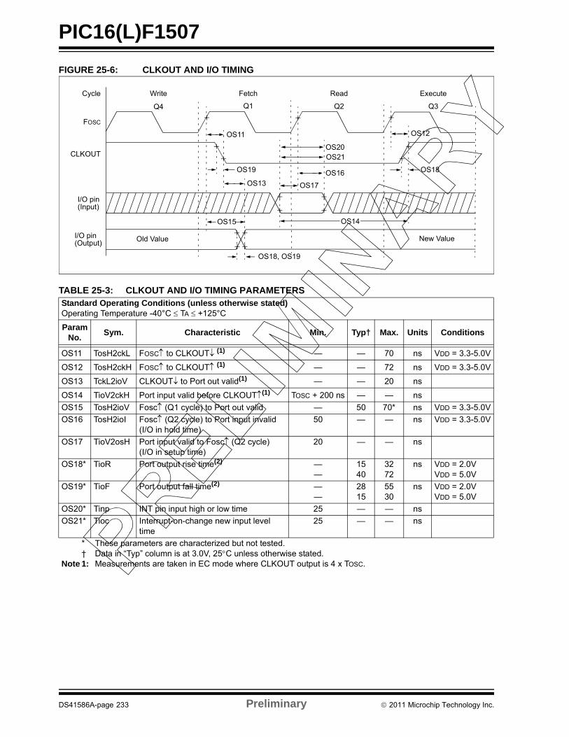
PIC16(L)F1507
FIGURE 25-6: CLKOUT AND I/O TIMING
TABLE 25-3: CLKOUT AND I/O TIMING PARAMETERS Standard Operating Conditions (unless otherwise stated)Operating Temperature -40°C TA +125°C
Param No.
Sym. Characteristic Min. Typ† Max. Units Conditions
OS11 TosH2ckL FOSC to CLKOUT (1) — — 70 ns VDD = 3.3-5.0V
OS12 TosH2ckH FOSC to CLKOUT (1) — — 72 ns VDD = 3.3-5.0V
OS13 TckL2ioV CLKOUT to Port out valid(1) — — 20 ns
OS14 TioV2ckH Port input valid before CLKOUT(1) TOSC + 200 ns — — ns
OS15 TosH2ioV Fosc (Q1 cycle) to Port out valid — 50 70* ns VDD = 3.3-5.0V
OS16 TosH2ioI Fosc (Q2 cycle) to Port input invalid (I/O in hold time)
50 — — ns VDD = 3.3-5.0V
OS17 TioV2osH Port input valid to Fosc(Q2 cycle)(I/O in setup time)
20 — — ns
OS18* TioR Port output rise time(2) ——
1540
3272
ns VDD = 2.0VVDD = 5.0V
OS19* TioF Port output fall time(2) ——
2815
5530
ns VDD = 2.0VVDD = 5.0V
OS20* Tinp INT pin input high or low time 25 — — ns
OS21* Tioc Interrupt-on-change new input level time
25 — — ns
* These parameters are characterized but not tested.† Data in “Typ” column is at 3.0V, 25C unless otherwise stated.
Note 1: Measurements are taken in EC mode where CLKOUT output is 4 x TOSC.
FOSC
CLKOUT
I/O pin(Input)
I/O pin(Output)
Q4 Q1 Q2 Q3
OS11
OS19
OS13
OS15
OS18, OS19
OS20OS21
OS17
OS16
OS14
OS12
OS18
Old Value New Value
Write Fetch Read ExecuteCycle
DS41586A-page 233 Preliminary 2011 Microchip Technology Inc.
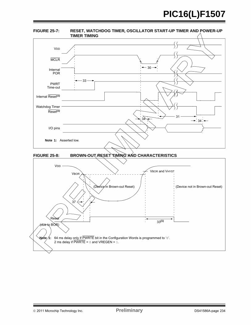
PIC16(L)F1507
FIGURE 25-7: RESET, WATCHDOG TIMER, OSCILLATOR START-UP TIMER AND POWER-UP TIMER TIMING
FIGURE 25-8: BROWN-OUT RESET TIMING AND CHARACTERISTICS
VDD
MCLR
InternalPOR
PWRTTime-out
Internal Reset(1)
Watchdog Timer
33
30
3134
I/O pins
34
Note 1: Asserted low.
Reset(1)
VBOR
VDD
(Device in Brown-out Reset) (Device not in Brown-out Reset)
33(1)
Note 1: 64 ms delay only if PWRTE bit in the Configuration Words is programmed to ‘0’. 2 ms delay if PWRTE = 0 and VREGEN = 1.
Reset
(due to BOR)
VBOR and VHYST
37
2011 Microchip Technology Inc. Preliminary DS41586A-page 234
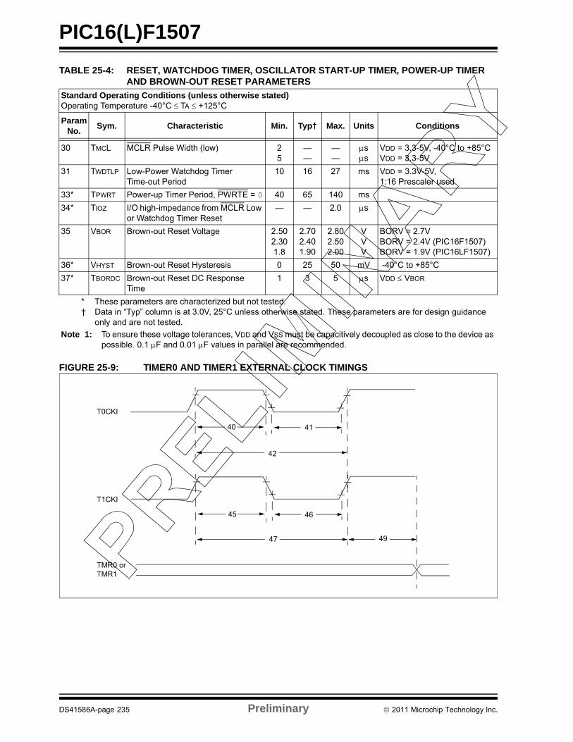
PIC16(L)F1507
TABLE 25-4: RESET, WATCHDOG TIMER, OSCILLATOR START-UP TIMER, POWER-UP TIMER AND BROWN-OUT RESET PARAMETERS
FIGURE 25-9: TIMER0 AND TIMER1 EXTERNAL CLOCK TIMINGS
Standard Operating Conditions (unless otherwise stated)Operating Temperature -40°C TA +125°C
Param No.
Sym. Characteristic Min. Typ† Max. Units Conditions
30 TMCL MCLR Pulse Width (low) 2 5
——
——
ss
VDD = 3.3-5V, -40°C to +85°CVDD = 3.3-5V
31 TWDTLP Low-Power Watchdog Timer Time-out Period
10 16 27 ms VDD = 3.3V-5V,1:16 Prescaler used
33* TPWRT Power-up Timer Period, PWRTE = 0 40 65 140 ms
34* TIOZ I/O high-impedance from MCLR Low or Watchdog Timer Reset
— — 2.0 s
35 VBOR Brown-out Reset Voltage 2.502.301.8
2.702.401.90
2.802.502.00
VVV
BORV = 2.7VBORV = 2.4V (PIC16F1507)BORV = 1.9V (PIC16LF1507)
36* VHYST Brown-out Reset Hysteresis 0 25 50 mV -40°C to +85°C
37* TBORDC Brown-out Reset DC Response Time
1 3 5 s VDD VBOR
* These parameters are characterized but not tested.† Data in “Typ” column is at 3.0V, 25°C unless otherwise stated. These parameters are for design guidance
only and are not tested.
Note 1: To ensure these voltage tolerances, VDD and VSS must be capacitively decoupled as close to the device as possible. 0.1 F and 0.01 F values in parallel are recommended.
T0CKI
T1CKI
40 41
42
45 46
47 49
TMR0 orTMR1
DS41586A-page 235 Preliminary 2011 Microchip Technology Inc.
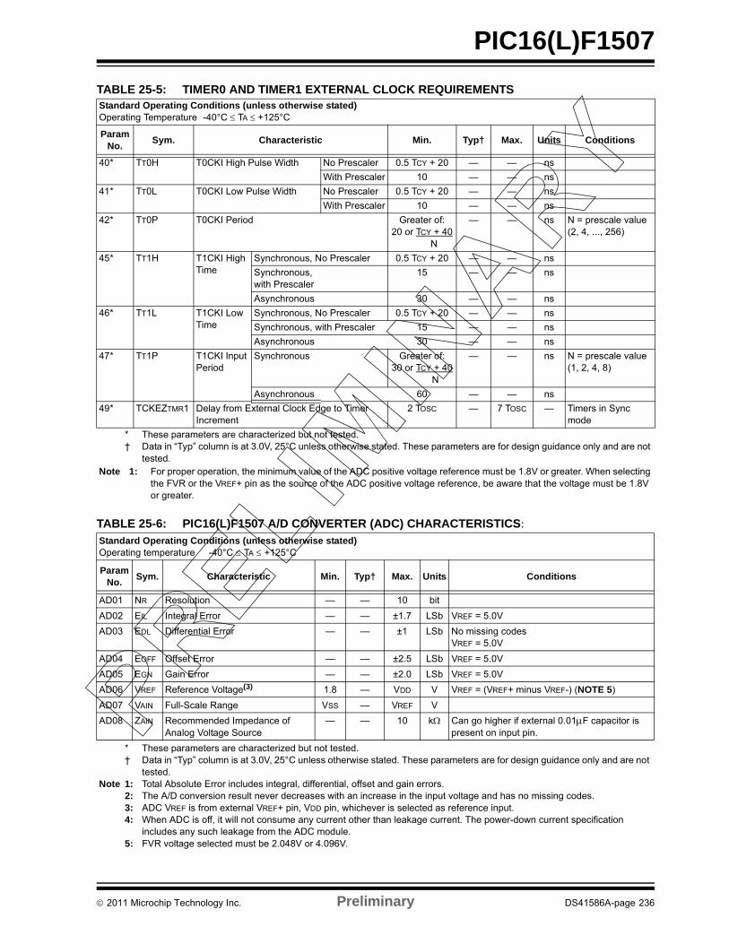
PIC16(L)F1507
TABLE 25-5: TIMER0 AND TIMER1 EXTERNAL CLOCK REQUIREMENTS
TABLE 25-6: PIC16(L)F1507 A/D CONVERTER (ADC) CHARACTERISTICS:
Standard Operating Conditions (unless otherwise stated)Operating Temperature -40°C TA +125°C
Param No.
Sym. Characteristic Min. Typ† Max. Units Conditions
40* TT0H T0CKI High Pulse Width No Prescaler 0.5 TCY + 20 — — ns
With Prescaler 10 — — ns
41* TT0L T0CKI Low Pulse Width No Prescaler 0.5 TCY + 20 — — ns
With Prescaler 10 — — ns
42* TT0P T0CKI Period Greater of:20 or TCY + 40
N
— — ns N = prescale value (2, 4, ..., 256)
45* TT1H T1CKI High Time
Synchronous, No Prescaler 0.5 TCY + 20 — — ns
Synchronous, with Prescaler
15 — — ns
Asynchronous 30 — — ns
46* TT1L T1CKI Low Time
Synchronous, No Prescaler 0.5 TCY + 20 — — ns
Synchronous, with Prescaler 15 — — ns
Asynchronous 30 — — ns
47* TT1P T1CKI Input Period
Synchronous Greater of:30 or TCY + 40
N
— — ns N = prescale value (1, 2, 4, 8)
Asynchronous 60 — — ns
49* TCKEZTMR1 Delay from External Clock Edge to Timer Increment
2 TOSC — 7 TOSC — Timers in Sync mode
* These parameters are characterized but not tested.† Data in “Typ” column is at 3.0V, 25°C unless otherwise stated. These parameters are for design guidance only and are not
tested.Note 1: For proper operation, the minimum value of the ADC positive voltage reference must be 1.8V or greater. When selecting
the FVR or the VREF+ pin as the source of the ADC positive voltage reference, be aware that the voltage must be 1.8V or greater.
Standard Operating Conditions (unless otherwise stated)Operating temperature -40°C TA +125°C
Param No.
Sym. Characteristic Min. Typ† Max. Units Conditions
AD01 NR Resolution — — 10 bit
AD02 EIL Integral Error — — ±1.7 LSb VREF = 5.0V
AD03 EDL Differential Error — — ±1 LSb No missing codesVREF = 5.0V
AD04 EOFF Offset Error — — ±2.5 LSb VREF = 5.0V
AD05 EGN Gain Error — — ±2.0 LSb VREF = 5.0V
AD06 VREF Reference Voltage(3) 1.8 — VDD V VREF = (VREF+ minus VREF-) (NOTE 5)
AD07 VAIN Full-Scale Range VSS — VREF V
AD08 ZAIN Recommended Impedance of Analog Voltage Source
— — 10 k Can go higher if external 0.01F capacitor is present on input pin.
* These parameters are characterized but not tested.† Data in “Typ” column is at 3.0V, 25°C unless otherwise stated. These parameters are for design guidance only and are not
tested.Note 1: Total Absolute Error includes integral, differential, offset and gain errors.
2: The A/D conversion result never decreases with an increase in the input voltage and has no missing codes.3: ADC VREF is from external VREF+ pin, VDD pin, whichever is selected as reference input.4: When ADC is off, it will not consume any current other than leakage current. The power-down current specification
includes any such leakage from the ADC module.5: FVR voltage selected must be 2.048V or 4.096V.
2011 Microchip Technology Inc. Preliminary DS41586A-page 236
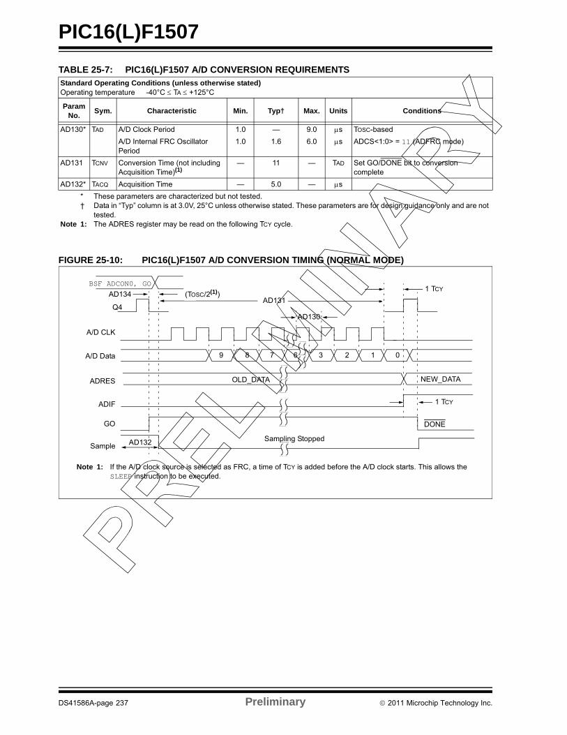
PIC16(L)F1507
TABLE 25-7: PIC16(L)F1507 A/D CONVERSION REQUIREMENTS
FIGURE 25-10: PIC16(L)F1507 A/D CONVERSION TIMING (NORMAL MODE)
Standard Operating Conditions (unless otherwise stated)Operating temperature -40°C TA +125°C
ParamNo.
Sym. Characteristic Min. Typ† Max. Units Conditions
AD130* TAD A/D Clock Period 1.0 — 9.0 s TOSC-based
A/D Internal FRC Oscillator Period
1.0 1.6 6.0 s ADCS<1:0> = 11 (ADFRC mode)
AD131 TCNV Conversion Time (not including Acquisition Time)(1)
— 11 — TAD Set GO/DONE bit to conversioncomplete
AD132* TACQ Acquisition Time — 5.0 — s
* These parameters are characterized but not tested.† Data in “Typ” column is at 3.0V, 25°C unless otherwise stated. These parameters are for design guidance only and are not
tested.Note 1: The ADRES register may be read on the following TCY cycle.
AD131
AD130
BSF ADCON0, GO
Q4
A/D CLK
A/D Data
ADRES
ADIF
GO
Sample
OLD_DATA
Sampling Stopped
DONE
NEW_DATA
9 8 7 3 2 1 0
Note 1: If the A/D clock source is selected as FRC, a time of TCY is added before the A/D clock starts. This allows the SLEEP instruction to be executed.
1 TCY
6
AD134 (TOSC/2(1))
1 TCY
AD132
DS41586A-page 237 Preliminary 2011 Microchip Technology Inc.
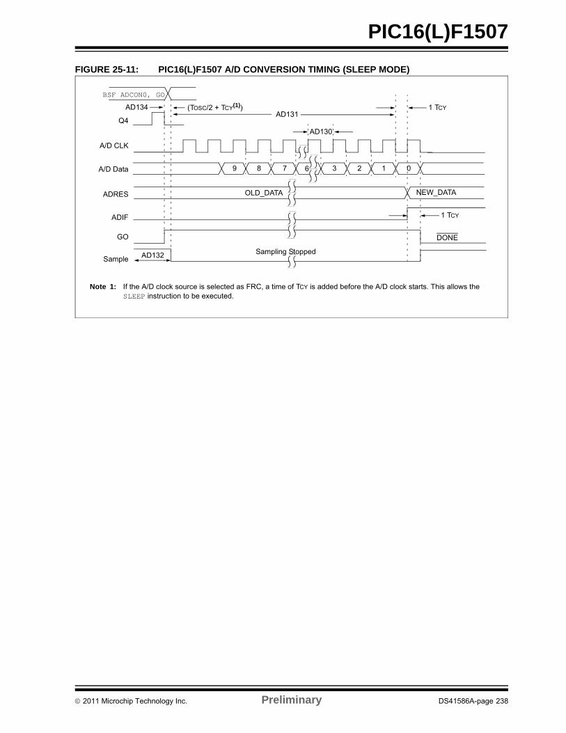
PIC16(L)F1507
FIGURE 25-11: PIC16(L)F1507 A/D CONVERSION TIMING (SLEEP MODE)
AD132
AD131
AD130
BSF ADCON0, GO
Q4
A/D CLK
A/D Data
ADRES
ADIF
GO
Sample
OLD_DATA
Sampling Stopped
DONE
NEW_DATA
9 7 3 2 1 0
Note 1: If the A/D clock source is selected as FRC, a time of TCY is added before the A/D clock starts. This allows the SLEEP instruction to be executed.
AD134
68
1 TCY(TOSC/2 + TCY(1))
1 TCY
2011 Microchip Technology Inc. Preliminary DS41586A-page 238
PIC16(L)F1507
26.0 DC AND AC CHARACTERISTICS GRAPHS AND CHARTS
Graphs and charts are not available at this time.
DS41586A-page 239 Preliminary 2011 Microchip Technology Inc.

PIC16(L)F1507
NOTES:
2011 Microchip Technology Inc. Preliminary DS41586A-page 240
PIC16(L)F1507
27.0 DEVELOPMENT SUPPORT
The PIC® microcontrollers and dsPIC® digital signalcontrollers are supported with a full range of softwareand hardware development tools:
• Integrated Development Environment
- MPLAB® IDE Software
• Compilers/Assemblers/Linkers
- MPLAB C Compiler for Various DeviceFamilies
- HI-TECH C for Various Device Families
- MPASMTM Assembler
- MPLINKTM Object Linker/MPLIBTM Object Librarian
- MPLAB Assembler/Linker/Librarian forVarious Device Families
• Simulators
- MPLAB SIM Software Simulator
• Emulators
- MPLAB REAL ICE™ In-Circuit Emulator
• In-Circuit Debuggers
- MPLAB ICD 3
- PICkit™ 3 Debug Express
• Device Programmers
- PICkit™ 2 Programmer
- MPLAB PM3 Device Programmer
• Low-Cost Demonstration/Development Boards, Evaluation Kits, and Starter Kits
27.1 MPLAB Integrated Development Environment Software
The MPLAB IDE software brings an ease of softwaredevelopment previously unseen in the 8/16/32-bitmicrocontroller market. The MPLAB IDE is a Windows®
operating system-based application that contains:
• A single graphical interface to all debugging tools
- Simulator
- Programmer (sold separately)
- In-Circuit Emulator (sold separately)
- In-Circuit Debugger (sold separately)
• A full-featured editor with color-coded context
• A multiple project manager
• Customizable data windows with direct edit of contents
• High-level source code debugging
• Mouse over variable inspection
• Drag and drop variables from source to watch windows
• Extensive on-line help
• Integration of select third party tools, such as IAR C Compilers
The MPLAB IDE allows you to:
• Edit your source files (either C or assembly)
• One-touch compile or assemble, and download to emulator and simulator tools (automatically updates all project information)
• Debug using:
- Source files (C or assembly)
- Mixed C and assembly
- Machine code
MPLAB IDE supports multiple debugging tools in asingle development paradigm, from the cost-effectivesimulators, through low-cost in-circuit debuggers, tofull-featured emulators. This eliminates the learningcurve when upgrading to tools with increased flexibilityand power.
DS41586A-page 241 Preliminary 2011 Microchip Technology Inc.
PIC16(L)F1507
27.2 MPLAB C Compilers for Various Device Families
The MPLAB C Compiler code development systemsare complete ANSI C compilers for Microchip’s PIC18,PIC24 and PIC32 families of microcontrollers and thedsPIC30 and dsPIC33 families of digital signal control-lers. These compilers provide powerful integrationcapabilities, superior code optimization and ease ofuse.
For easy source level debugging, the compilers providesymbol information that is optimized to the MPLAB IDEdebugger.
27.3 HI-TECH C for Various Device Families
The HI-TECH C Compiler code development systemsare complete ANSI C compilers for Microchip’s PICfamily of microcontrollers and the dsPIC family of digitalsignal controllers. These compilers provide powerfulintegration capabilities, omniscient code generationand ease of use.
For easy source level debugging, the compilers providesymbol information that is optimized to the MPLAB IDEdebugger.
The compilers include a macro assembler, linker, pre-processor, and one-step driver, and can run on multipleplatforms.
27.4 MPASM Assembler
The MPASM Assembler is a full-featured, universalmacro assembler for PIC10/12/16/18 MCUs.
The MPASM Assembler generates relocatable objectfiles for the MPLINK Object Linker, Intel® standard HEXfiles, MAP files to detail memory usage and symbolreference, absolute LST files that contain source linesand generated machine code and COFF files fordebugging.
The MPASM Assembler features include:
• Integration into MPLAB IDE projects
• User-defined macros to streamline assembly code
• Conditional assembly for multi-purpose source files
• Directives that allow complete control over the assembly process
27.5 MPLINK Object Linker/MPLIB Object Librarian
The MPLINK Object Linker combines relocatableobjects created by the MPASM Assembler and theMPLAB C18 C Compiler. It can link relocatable objectsfrom precompiled libraries, using directives from alinker script.
The MPLIB Object Librarian manages the creation andmodification of library files of precompiled code. Whena routine from a library is called from a source file, onlythe modules that contain that routine will be linked inwith the application. This allows large libraries to beused efficiently in many different applications.
The object linker/library features include:
• Efficient linking of single libraries instead of many smaller files
• Enhanced code maintainability by grouping related modules together
• Flexible creation of libraries with easy module listing, replacement, deletion and extraction
27.6 MPLAB Assembler, Linker and Librarian for Various Device Families
MPLAB Assembler produces relocatable machinecode from symbolic assembly language for PIC24,PIC32 and dsPIC devices. MPLAB C Compiler usesthe assembler to produce its object file. The assemblergenerates relocatable object files that can then bearchived or linked with other relocatable object files andarchives to create an executable file. Notable featuresof the assembler include:
• Support for the entire device instruction set
• Support for fixed-point and floating-point data
• Command line interface
• Rich directive set
• Flexible macro language
• MPLAB IDE compatibility
2011 Microchip Technology Inc. Preliminary DS41586A-page 242
PIC16(L)F1507
27.7 MPLAB SIM Software Simulator
The MPLAB SIM Software Simulator allows codedevelopment in a PC-hosted environment by simulat-ing the PIC MCUs and dsPIC® DSCs on an instructionlevel. On any given instruction, the data areas can beexamined or modified and stimuli can be applied froma comprehensive stimulus controller. Registers can belogged to files for further run-time analysis. The tracebuffer and logic analyzer display extend the power ofthe simulator to record and track program execution,actions on I/O, most peripherals and internal registers.
The MPLAB SIM Software Simulator fully supportssymbolic debugging using the MPLAB C Compilers,and the MPASM and MPLAB Assemblers. The soft-ware simulator offers the flexibility to develop anddebug code outside of the hardware laboratory envi-ronment, making it an excellent, economical softwaredevelopment tool.
27.8 MPLAB REAL ICE In-Circuit Emulator System
MPLAB REAL ICE In-Circuit Emulator System isMicrochip’s next generation high-speed emulator forMicrochip Flash DSC and MCU devices. It debugs andprograms PIC® Flash MCUs and dsPIC® Flash DSCswith the easy-to-use, powerful graphical user interface ofthe MPLAB Integrated Development Environment (IDE),included with each kit.
The emulator is connected to the design engineer’s PCusing a high-speed USB 2.0 interface and is connectedto the target with either a connector compatible with in-circuit debugger systems (RJ11) or with the new high-speed, noise tolerant, Low-Voltage Differential Signal(LVDS) interconnection (CAT5).
The emulator is field upgradable through future firmwaredownloads in MPLAB IDE. In upcoming releases ofMPLAB IDE, new devices will be supported, and newfeatures will be added. MPLAB REAL ICE offerssignificant advantages over competitive emulatorsincluding low-cost, full-speed emulation, run-timevariable watches, trace analysis, complex breakpoints, aruggedized probe interface and long (up to three meters)interconnection cables.
27.9 MPLAB ICD 3 In-Circuit Debugger System
MPLAB ICD 3 In-Circuit Debugger System is Micro-chip's most cost effective high-speed hardwaredebugger/programmer for Microchip Flash Digital Sig-nal Controller (DSC) and microcontroller (MCU)devices. It debugs and programs PIC® Flash microcon-trollers and dsPIC® DSCs with the powerful, yet easy-to-use graphical user interface of MPLAB IntegratedDevelopment Environment (IDE).
The MPLAB ICD 3 In-Circuit Debugger probe is con-nected to the design engineer's PC using a high-speedUSB 2.0 interface and is connected to the target with aconnector compatible with the MPLAB ICD 2 or MPLABREAL ICE systems (RJ-11). MPLAB ICD 3 supports allMPLAB ICD 2 headers.
27.10 PICkit 3 In-Circuit Debugger/Programmer and PICkit 3 Debug Express
The MPLAB PICkit 3 allows debugging and program-ming of PIC® and dsPIC® Flash microcontrollers at amost affordable price point using the powerful graphicaluser interface of the MPLAB Integrated DevelopmentEnvironment (IDE). The MPLAB PICkit 3 is connectedto the design engineer's PC using a full speed USBinterface and can be connected to the target via anMicrochip debug (RJ-11) connector (compatible withMPLAB ICD 3 and MPLAB REAL ICE). The connectoruses two device I/O pins and the reset line to imple-ment in-circuit debugging and In-Circuit Serial Pro-gramming™.
The PICkit 3 Debug Express include the PICkit 3, demoboard and microcontroller, hookup cables and CDROMwith user’s guide, lessons, tutorial, compiler andMPLAB IDE software.
DS41586A-page 243 Preliminary 2011 Microchip Technology Inc.
PIC16(L)F1507
27.11 PICkit 2 Development Programmer/Debugger and PICkit 2 Debug Express
The PICkit™ 2 Development Programmer/Debugger isa low-cost development tool with an easy to use inter-face for programming and debugging Microchip’s Flashfamilies of microcontrollers. The full featuredWindows® programming interface supports baseline(PIC10F, PIC12F5xx, PIC16F5xx), midrange(PIC12F6xx, PIC16F), PIC18F, PIC24, dsPIC30,dsPIC33, and PIC32 families of 8-bit, 16-bit, and 32-bitmicrocontrollers, and many Microchip Serial EEPROMproducts. With Microchip’s powerful MPLAB IntegratedDevelopment Environment (IDE) the PICkit™ 2enables in-circuit debugging on most PIC® microcon-trollers. In-Circuit-Debugging runs, halts and singlesteps the program while the PIC microcontroller isembedded in the application. When halted at a break-point, the file registers can be examined and modified.
The PICkit 2 Debug Express include the PICkit 2, demoboard and microcontroller, hookup cables and CDROMwith user’s guide, lessons, tutorial, compiler andMPLAB IDE software.
27.12 MPLAB PM3 Device Programmer
The MPLAB PM3 Device Programmer is a universal,CE compliant device programmer with programmablevoltage verification at VDDMIN and VDDMAX formaximum reliability. It features a large LCD display(128 x 64) for menus and error messages and a modu-lar, detachable socket assembly to support variouspackage types. The ICSP™ cable assembly is includedas a standard item. In Stand-Alone mode, the MPLABPM3 Device Programmer can read, verify and programPIC devices without a PC connection. It can also setcode protection in this mode. The MPLAB PM3connects to the host PC via an RS-232 or USB cable.The MPLAB PM3 has high-speed communications andoptimized algorithms for quick programming of largememory devices and incorporates an MMC card for filestorage and data applications.
27.13 Demonstration/Development Boards, Evaluation Kits, and Starter Kits
A wide variety of demonstration, development andevaluation boards for various PIC MCUs and dsPICDSCs allows quick application development on fully func-tional systems. Most boards include prototyping areas foradding custom circuitry and provide application firmwareand source code for examination and modification.
The boards support a variety of features, including LEDs,temperature sensors, switches, speakers, RS-232interfaces, LCD displays, potentiometers and additionalEEPROM memory.
The demonstration and development boards can beused in teaching environments, for prototyping customcircuits and for learning about various microcontrollerapplications.
In addition to the PICDEM™ and dsPICDEM™ demon-stration/development board series of circuits, Microchiphas a line of evaluation kits and demonstration softwarefor analog filter design, KEELOQ® security ICs, CAN,IrDA®, PowerSmart battery management, SEEVAL®
evaluation system, Sigma-Delta ADC, flow ratesensing, plus many more.
Also available are starter kits that contain everythingneeded to experience the specified device. This usuallyincludes a single application and debug capability, allon one board.
Check the Microchip web page (www.microchip.com)for the complete list of demonstration, developmentand evaluation kits.
2011 Microchip Technology Inc. Preliminary DS41586A-page 244
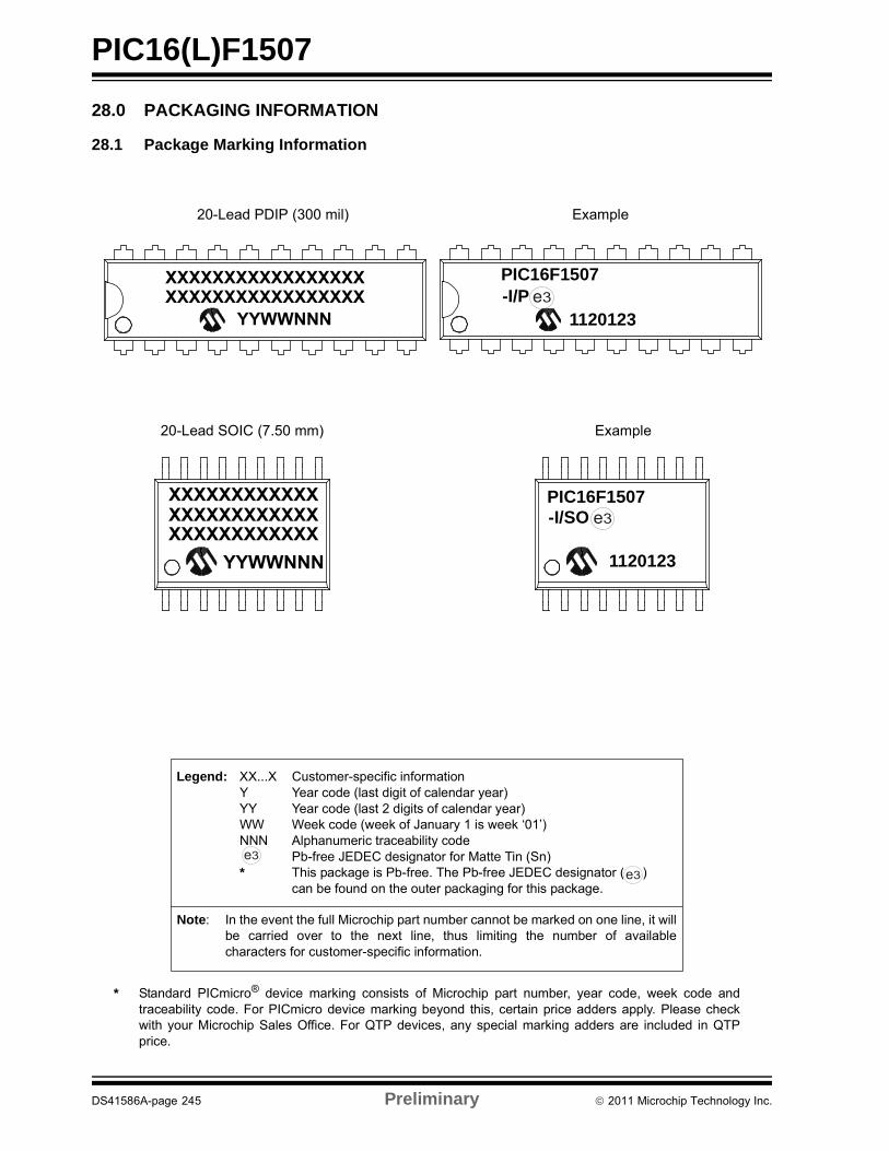
PIC16(L)F1507
28.0 PACKAGING INFORMATION
28.1 Package Marking Information
* Standard PICmicro® device marking consists of Microchip part number, year code, week code andtraceability code. For PICmicro device marking beyond this, certain price adders apply. Please checkwith your Microchip Sales Office. For QTP devices, any special marking adders are included in QTPprice.
Legend: XX...X Customer-specific informationY Year code (last digit of calendar year)YY Year code (last 2 digits of calendar year)WW Week code (week of January 1 is week ‘01’)NNN Alphanumeric traceability code Pb-free JEDEC designator for Matte Tin (Sn)* This package is Pb-free. The Pb-free JEDEC designator ( )
can be found on the outer packaging for this package.
Note: In the event the full Microchip part number cannot be marked on one line, it willbe carried over to the next line, thus limiting the number of availablecharacters for customer-specific information.
3e
3e
20-Lead PDIP (300 mil) Example
XXXXXXXXXXXXXXXXXXXXXXXXXXXXXXXXXX
YYWWNNN
20-Lead SOIC (7.50 mm) Example
XXXXXXXXXXXX
YYWWNNN
XXXXXXXXXXXXXXXXXXXXXXXX
PIC16F1507-I/P 3e
1120123
PIC16F1507-I/SO 3e
1120123
DS41586A-page 245 Preliminary 2011 Microchip Technology Inc.
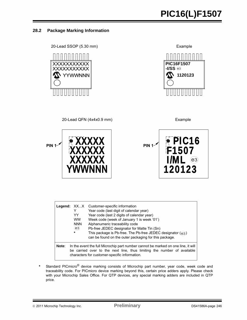
PIC16(L)F1507
28.2 Package Marking Information
* Standard PICmicro® device marking consists of Microchip part number, year code, week code andtraceability code. For PICmicro device marking beyond this, certain price adders apply. Please checkwith your Microchip Sales Office. For QTP devices, any special marking adders are included in QTPprice.
Legend: XX...X Customer-specific informationY Year code (last digit of calendar year)YY Year code (last 2 digits of calendar year)WW Week code (week of January 1 is week ‘01’)NNN Alphanumeric traceability code Pb-free JEDEC designator for Matte Tin (Sn)* This package is Pb-free. The Pb-free JEDEC designator ( )
can be found on the outer packaging for this package.
Note: In the event the full Microchip part number cannot be marked on one line, it willbe carried over to the next line, thus limiting the number of availablecharacters for customer-specific information.
3e
3e
20-Lead SSOP (5.30 mm) Example
20-Lead QFN (4x4x0.9 mm) Example
PIN 1 PIN 1
-I/SS 3e
1120123
PIC16F1507
PIC16F1507I/ML
1201233e
2011 Microchip Technology Inc. Preliminary DS41586A-page 246
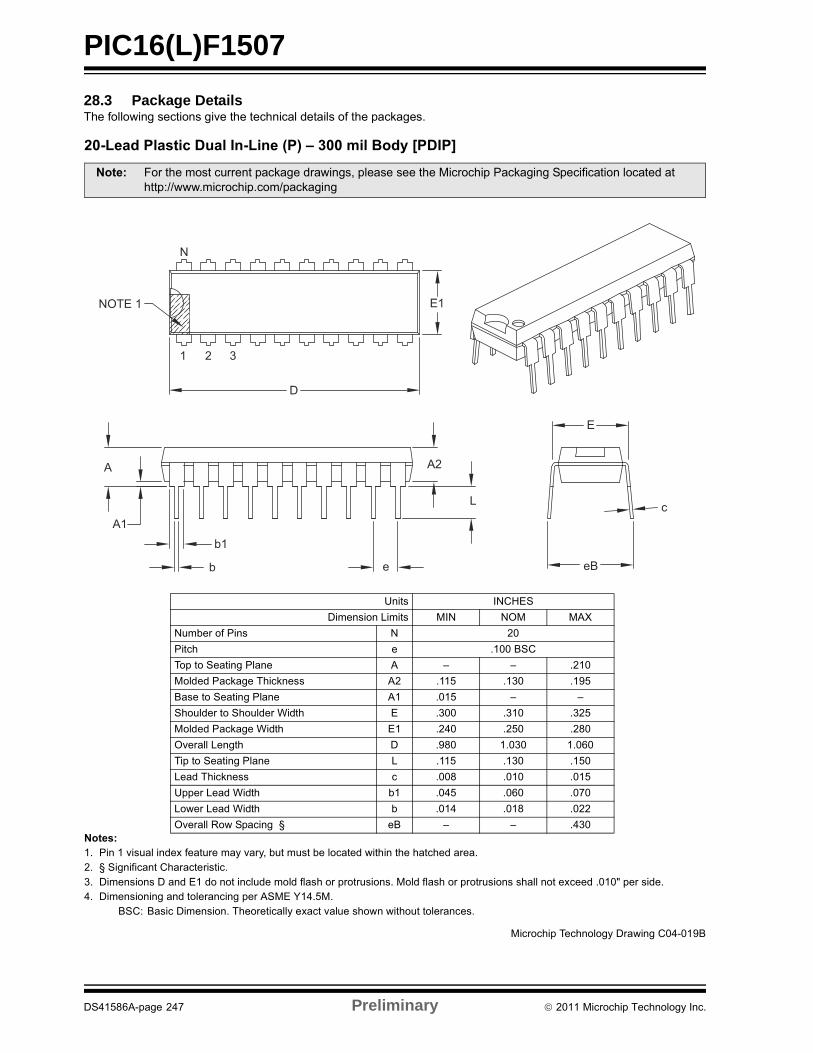
PIC16(L)F1507
28.3 Package DetailsThe following sections give the technical details of the packages.
���������� ������������������������������
�
�� ����� ������ �!"�����# $�% �&"� �'��� ���(�)"&�'"!&�) �����& #�*�&����&� ���&�� #��� ���� +������%����&�,�����& ��!&���-� ��' �!���!�����#�.��#����&�����"# �'��#�%��!�������&�"!���!�����#�%��!�������&�"!���!�!�������&� $� #�����/� ��!�# ��� ��' �!���������#�&�� �������� �����.�0������
1�,2 1�!�����' �!������� �� &������� $��&� ��" �!��*��*�&��"&�&�� ���� !�
�� �� 3���&� �'�!&��"�� �&���4�� �#��*���!(�� �! �! �&� �������������4������� ��%���&��������& #��&��&&255***�'����������'5��4�����
6��&! �7,8.���' �!����9�'�&! ��7 7:� ��;
7"') ���%����! 7 ����&�� �����1�,���&��� �&�������� � < < �������# #����4�� �����4� !! �� ���� ��-� ����1�! �&��� �&�������� �� ���� < <���"�# ��&�����"�# ��=�#&� . �-�� �-�� �-�����# #����4�� �=�#&� .� ���� ���� ��>�: �����9 ��&� � ��>� ���-� ���?����&��� �&�������� 9 ���� ��-� ����9 �#�����4� !! � ���> ���� ����6 ��9 �#�=�#&� )� ���� ��?� ����9�* ��9 �#�=�#&� ) ���� ���> ����: �������*���������+ 1 < < ��-�
N
E1NOTE 1
D
1 2 3
A
A1
A2
L
e
b1
b
E
c
eB
�������� � �������� ���*��� ,�����1
DS41586A-page 247 Preliminary 2011 Microchip Technology Inc.
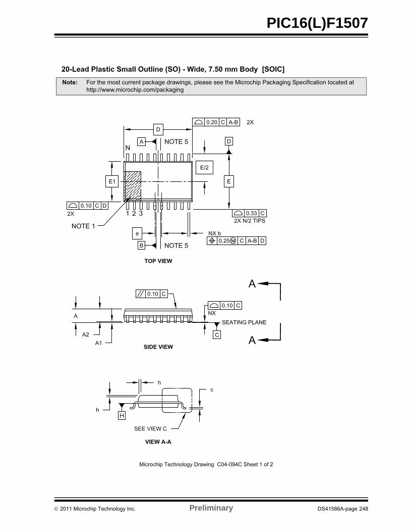
PIC16(L)F1507
Note: For the most current package drawings, please see the Microchip Packaging Specification located at http://www.microchip.com/packaging
2011 Microchip Technology Inc. Preliminary DS41586A-page 248
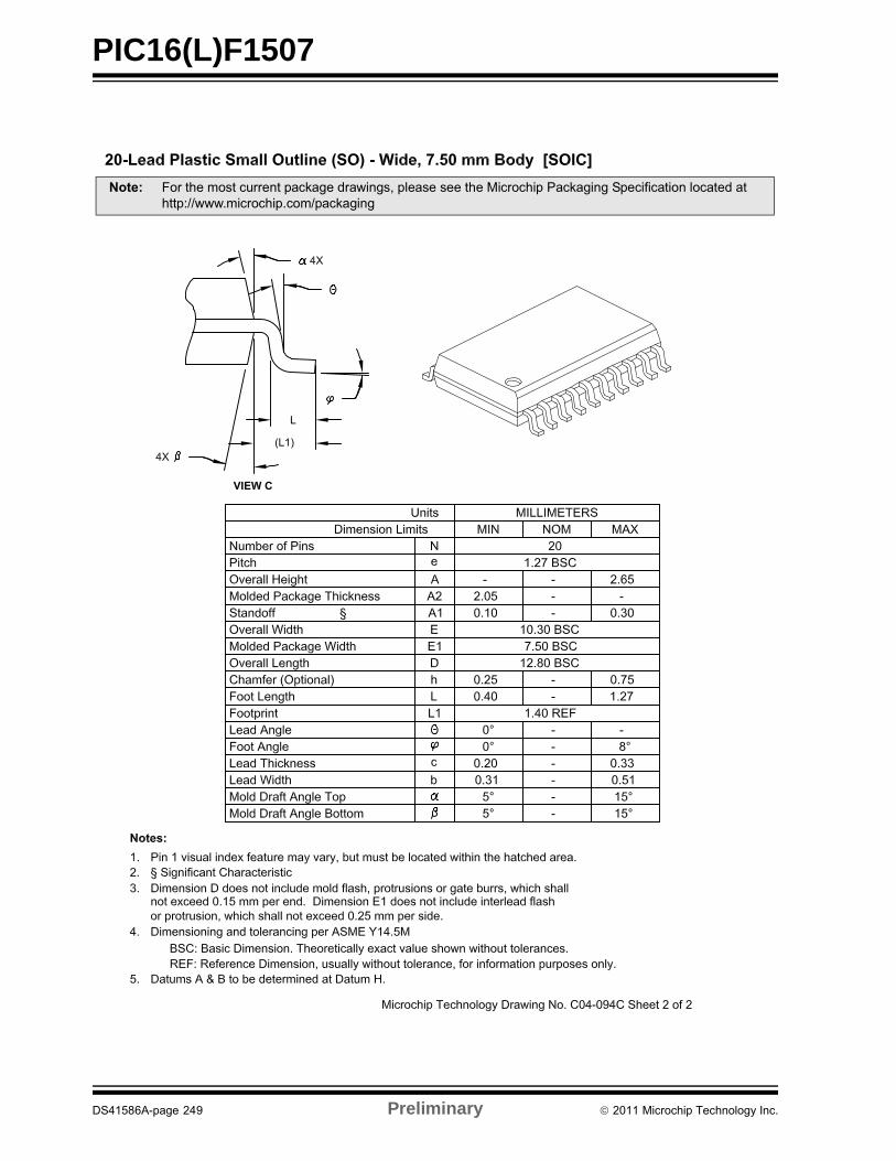
PIC16(L)F1507
Note: For the most current package drawings, please see the Microchip Packaging Specification located at http://www.microchip.com/packaging
DS41586A-page 249 Preliminary 2011 Microchip Technology Inc.
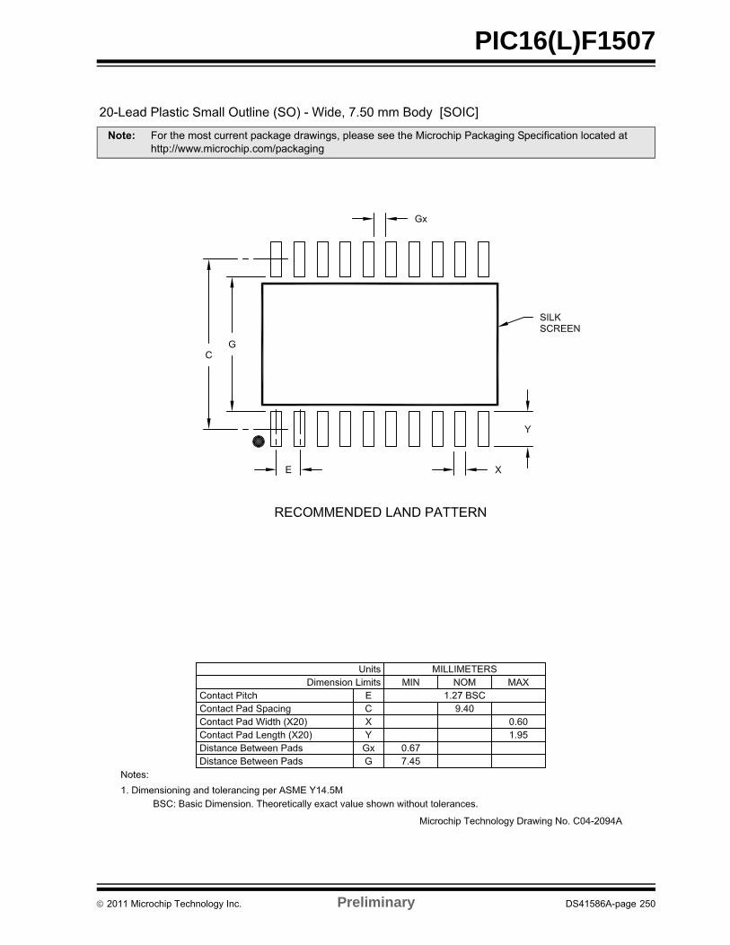
PIC16(L)F1507
Note: For the most current package drawings, please see the Microchip Packaging Specification located at http://www.microchip.com/packaging
2011 Microchip Technology Inc. Preliminary DS41586A-page 250
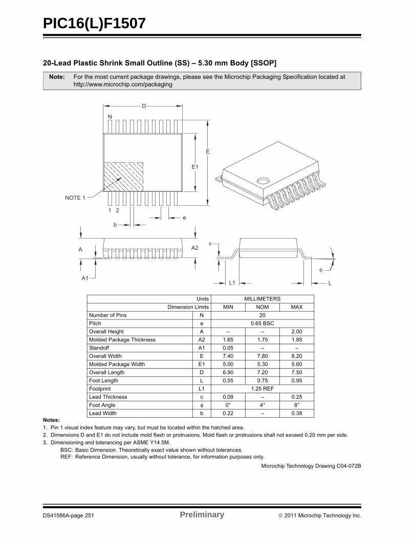
PIC16(L)F1507
���������� �� !"��# ����$� ����� ��%&��������� $�
�� ����� ������ �!"�����# $�% �&"� �'��� ���(�)"&�'"!&�) �����& #�*�&����&� ���&�� #��� ���� ��' �!���!�����#�.��#����&�����"# �'��#�%��!�������&�"!���!�����#�%��!�������&�"!���!�!�������&� $� #������''� ��!�# �-� ��' �!���������#�&�� �������� �����.�0������
1�,2 1�!�����' �!������� �� &������� $��&� ��" �!��*��*�&��"&�&�� ���� !��.32 � % � �� ���' �!���(�"!"�����*�&��"&�&�� ���� (�%�����%��'�&����"��! !������
�� �� 3���&� �'�!&��"�� �&���4�� �#��*���!(�� �! �! �&� �������������4������� ��%���&��������& #��&��&&255***�'����������'5��4�����
6��&! ��99��.�.����' �!����9�'�&! ��7 7:� ��;
7"') ���%����! 7 ����&�� ��?��1�,: �����8 ���& � < < �������# #����4�� �����4� !! �� ��?� ���� ��>��&��#�%%� �� ���� < <: �����=�#&� . ���� ��>� >������# #����4�� �=�#&� .� ���� ��-� ��?�: �����9 ��&� � ?��� ���� ����3��&�9 ��&� 9 ���� ���� ����3��&���& 9� ������.39 �#�����4� !! � ���� < ����3��&����� � �@ �@ >@9 �#�=�#&� ) ���� < ��->
φ
LL1
A2c
eb
A1
A
1 2
NOTE 1
E1
E
D
N
�������� � �������� ���*��� ,�����1
DS41586A-page 251 Preliminary 2011 Microchip Technology Inc.
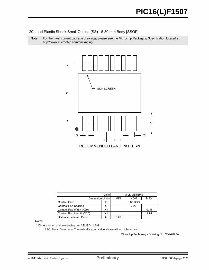
PIC16(L)F1507
Note: For the most current package drawings, please see the Microchip Packaging Specification located at http://www.microchip.com/packaging
2011 Microchip Technology Inc. Preliminary DS41586A-page 252
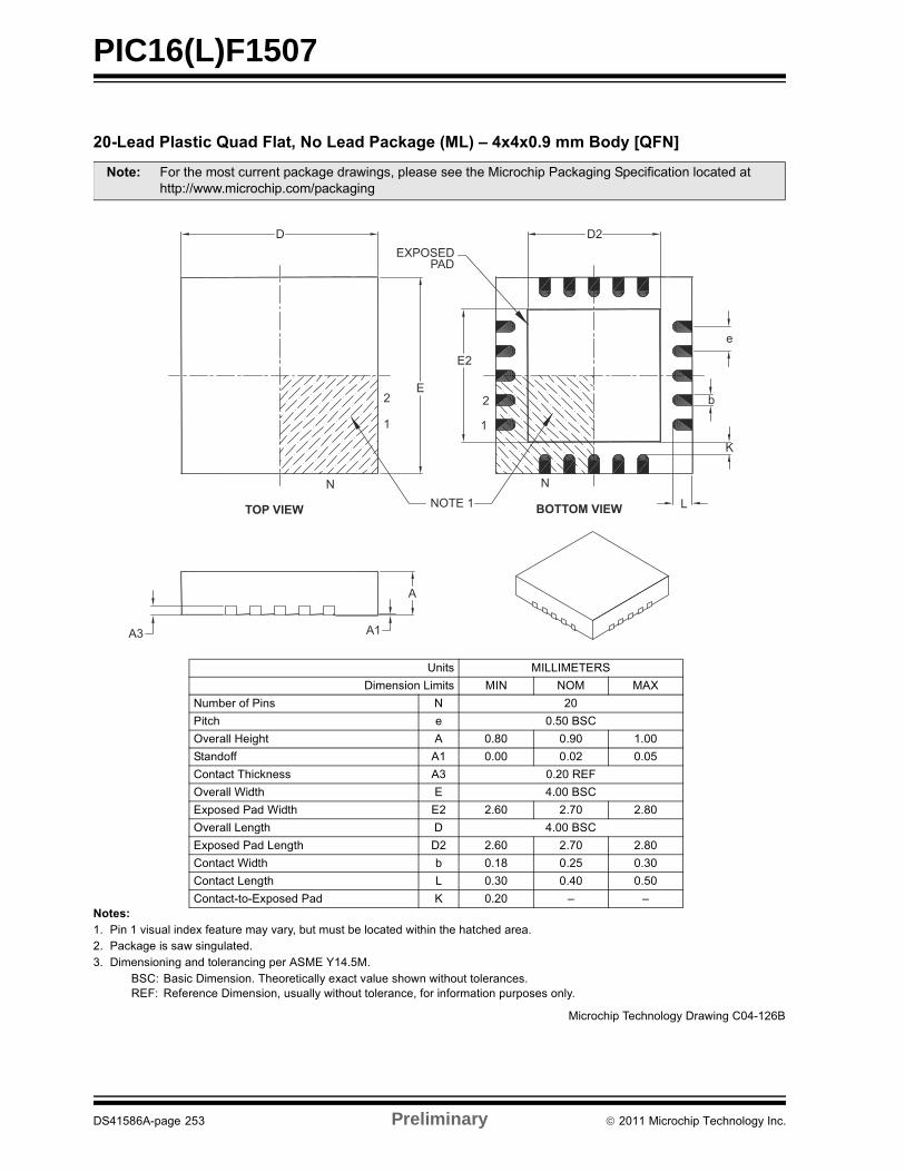
PIC16(L)F1507
���������� ��'���(�� )��������#�*��+���,-,-�&.�������'(��
�
�� ����� ������ �!"�����# $�% �&"� �'��� ���(�)"&�'"!&�) �����& #�*�&����&� ���&�� #��� ���� ���4�� ��!�!�*�!���"��& #�-� ��' �!���������#�&�� �������� �����.�0������
1�,2 1�!�����' �!������� �� &������� $��&� ��" �!��*��*�&��"&�&�� ���� !��.32 � % � �� ���' �!���(�"!"�����*�&��"&�&�� ���� (�%�����%��'�&����"��! !������
�� �� 3���&� �'�!&��"�� �&���4�� �#��*���!(�� �! �! �&� �������������4������� ��%���&��������& #��&��&&255***�'����������'5��4�����
6��&! ��99��.�.����' �!����9�'�&! ��7 7:� ��;
7"') ���%����! 7 ����&�� �����1�,: �����8 ���& � ��>� ���� �����&��#�%%� �� ���� ���� ����,��&��&�����4� !! �- ������.3: �����=�#&� . �����1�,.$�! #���#�=�#&� .� ��?� ���� ��>�: �����9 ��&� � �����1�,.$�! #���#�9 ��&� �� ��?� ���� ��>�,��&��&�=�#&� ) ���> ���� ��-�,��&��&�9 ��&� 9 ��-� ���� ����,��&��&&�.$�! #���# A ���� < <
DEXPOSED
PAD
E
E2
2
1
N
TOP VIEW NOTE 1
N
L
K
b
e
D2
2
1
A
A1A3
BOTTOM VIEW
�������� � �������� ���*��� ,����?1
DS41586A-page 253 Preliminary 2011 Microchip Technology Inc.
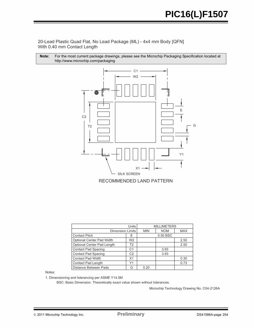
PIC16(L)F1507
�� �� 3���&� �'�!&��"�� �&���4�� �#��*���!(�� �! �! �&� �������������4������� ��%���&��������& #��&��&&255***�'����������'5��4�����
2011 Microchip Technology Inc. Preliminary DS41586A-page 254
PIC16(L)F1507
APPENDIX A: DATA SHEET REVISION HISTORY
Revision A
Original release (06/2011).
DS41586A-page 255 Preliminary 2011 Microchip Technology Inc.

PIC16(L)F1507
NOTES:
2011 Microchip Technology Inc. Preliminary DS41586A-page 256
PIC16(L)F1507
INDEX
AA/D
Specifications.................................................... 236, 237Absolute Maximum Ratings .............................................. 221AC Characteristics
Industrial and Extended ............................................ 232Load Conditions ........................................................ 231
ADC................................................................................... 121Acquisition Requirements ......................................... 132Associated registers.................................................. 134Block Diagram........................................................... 121Calculating Acquisition Time..................................... 132Channel Selection..................................................... 122Configuration............................................................. 122Configuring Interrupt ................................................. 126Conversion Clock...................................................... 122Conversion Procedure .............................................. 126Internal Sampling Switch (RSS) Impedance.............. 132Interrupts................................................................... 124Operation .................................................................. 125Operation During Sleep ............................................ 125Port Configuration ..................................................... 122Reference Voltage (VREF)......................................... 122Source Impedance.................................................... 132Starting an A/D Conversion ...................................... 124
ADCON0 Register....................................................... 25, 127ADCON1 Register....................................................... 25, 128ADCON2 Register............................................................. 129ADDFSR ........................................................................... 211ADDWFC .......................................................................... 211ADRESH Register............................................................... 25ADRESH Register (ADFM = 0) ......................................... 130ADRESH Register (ADFM = 1) ......................................... 131ADRESL Register (ADFM = 0).......................................... 130ADRESL Register (ADFM = 1).......................................... 131Alternate Pin Function....................................................... 100Analog-to-Digital Converter. See ADCANSELA Register.............................................................. 103ANSELB Register.............................................................. 107ANSELC Register ............................................................. 110APFCON Register............................................................. 100Assembler
MPASM Assembler ................................................... 242Automatic Context Saving................................................... 65
BBank 10 ............................................................................... 27Bank 11 ............................................................................... 27Bank 12 ............................................................................... 28Bank 13 ............................................................................... 28Bank 2 ................................................................................. 26Bank 3 ................................................................................. 26Bank 30 ............................................................................... 29Bank 4 ................................................................................. 26Bank 5 ................................................................................. 26Bank 6 ................................................................................. 26Bank 7 ................................................................................. 27Bank 8 ................................................................................. 27Bank 9 ................................................................................. 27Block Diagrams
ADC .......................................................................... 121ADC Transfer Function ............................................. 133Analog Input Model ................................................... 133
Clock Source .............................................................. 45Generic I/O Port.......................................................... 99Interrupt Logic............................................................. 61NCO.......................................................................... 178On-Chip Reset Circuit................................................. 53PIC16(L)F1507 ....................................................... 4, 10PWM......................................................................... 155Timer0 ...................................................................... 135Timer1 ...................................................................... 139Timer1 Gate.............................................. 144, 145, 146Timer2 ...................................................................... 151Voltage Reference.................................................... 117
BORCON Register.............................................................. 55BRA .................................................................................. 212Brown-out Reset (BOR)...................................................... 55
Specifications ........................................................... 235Timing and Characteristics ....................................... 234
CC Compilers
MPLAB C18.............................................................. 242CALL................................................................................. 213CALLW ............................................................................. 213CLCDATA Register........................................................... 175CLCxCON Register .......................................................... 167CLCxGLS0 Register ......................................................... 171CLCxGLS1 Register ......................................................... 172CLCxGLS2 Register ......................................................... 173CLCxGLS3 Register ......................................................... 174CLCxPOL Register ........................................................... 168CLCxSEL0 Register.......................................................... 169Clock Sources
External Modes........................................................... 46EC....................................................................... 46
Internal Modes............................................................ 47HFINTOSC ......................................................... 47Internal Oscillator Clock Switch Timing .............. 48LFINTOSC.......................................................... 47
Clock Switching .................................................................. 50Code Examples
A/D Conversion......................................................... 126Initializing PORTA..................................................... 101Writing to Flash Program Memory .............................. 92
ComparatorsC2OUT as T1 Gate................................................... 141
Complementary Waveform Generator (CWG).................. 187CONFIG1 Register ............................................................. 40CONFIG2 Register ............................................................. 41Core Function Register....................................................... 24Customer Change Notification Service............................. 262Customer Notification Service .......................................... 262Customer Support............................................................. 262CWG
Auto-shutdown Control ............................................. 194Clock Source ............................................................ 190Output Control .......................................................... 190Selectable Input Sources.......................................... 190
CWGxCON0 Register....................................................... 197CWGxCON1 Register....................................................... 198CWGxCON2 Register....................................................... 199CWGxDBF Register.......................................................... 200CWGxDBR Register ......................................................... 200
DS41586A-page 257 Preliminary 2011 Microchip Technology Inc.
PIC16(L)F1507
DData Memory ...................................................................... 17DC and AC Characteristics ............................................... 239DC Characteristics
Extended and Industrial ............................................ 228Industrial and Extended ............................................ 223
Development Support ....................................................... 241Device Configuration........................................................... 39
Code Protection .......................................................... 42Configuration Word ..................................................... 39User ID.................................................................. 42, 43
Device ID Register .............................................................. 43Device Overview ............................................................. 9, 79
EEffects of Reset
PWM mode ............................................................... 157Electrical Specifications .................................................... 221Enhanced Mid-Range CPU................................................. 13Extended Instruction Set
ADDFSR ................................................................... 211
FFirmware Instructions........................................................ 207Fixed Voltage Reference (FVR)........................................ 117
Associated Registers ................................................ 118Flash Program Memory ...................................................... 83
Associated Registers .................................................. 98Configuration Word w/ Flash Program Memory.......... 98Erasing........................................................................ 87Modifying..................................................................... 93Write Verify ................................................................. 95Writing......................................................................... 89
FSR Register ...................................................................... 24FVRCON (Fixed Voltage Reference Control) Register ..... 118
IINDF Register ..................................................................... 24Indirect Addressing ............................................................. 34Instruction Format ............................................................. 208Instruction Set ................................................................... 207
ADDLW ..................................................................... 211ADDWF..................................................................... 211ADDWFC .................................................................. 211ANDLW ..................................................................... 211ANDWF..................................................................... 211BRA........................................................................... 212CALL ......................................................................... 213CALLW...................................................................... 213LSLF ......................................................................... 215LSRF......................................................................... 215MOVF........................................................................ 215MOVIW ..................................................................... 216MOVLB ..................................................................... 216MOVWI ..................................................................... 217OPTION .................................................................... 217RESET ...................................................................... 217SUBWFB................................................................... 219TRIS.......................................................................... 220BCF........................................................................... 212BSF........................................................................... 212BTFSC ...................................................................... 212BTFSS ...................................................................... 212CALL ......................................................................... 213CLRF......................................................................... 213
CLRW ....................................................................... 213CLRWDT .................................................................. 213COMF ....................................................................... 213DECF........................................................................ 213DECFSZ ................................................................... 214GOTO ....................................................................... 214INCF ......................................................................... 214INCFSZ..................................................................... 214IORLW...................................................................... 214IORWF...................................................................... 214MOVLW .................................................................... 216MOVWF.................................................................... 216NOP.......................................................................... 217RETFIE..................................................................... 218RETLW ..................................................................... 218RETURN................................................................... 218RLF........................................................................... 218RRF .......................................................................... 219SLEEP ...................................................................... 219SUBLW..................................................................... 219SUBWF..................................................................... 219SWAPF..................................................................... 220XORLW .................................................................... 220XORWF .................................................................... 220
INTCON Register................................................................ 66Internal Oscillator Block
INTOSCSpecifications ................................................... 232
Internal Sampling Switch (RSS) Impedance ..................... 132Internet Address ............................................................... 262Interrupt-On-Change......................................................... 111
Associated Registers................................................ 115Interrupts ............................................................................ 61
ADC .......................................................................... 126Associated registers w/ Interrupts .............................. 73Configuration Word w/ Clock Sources........................ 52TMR1........................................................................ 143
INTOSC Specifications ..................................................... 232IOCAF Register ................................................................ 113IOCAN Register ................................................................ 113IOCAP Register ................................................................ 113IOCBF Register ................................................................ 114IOCBN Register ................................................................ 114IOCBP Register ................................................................ 114
LLATA Register .......................................................... 103, 109LATB Register .................................................................. 106Load Conditions................................................................ 231LSLF ................................................................................. 215LSRF ................................................................................ 215
MMCLR ................................................................................. 56
Internal........................................................................ 56Memory Organization ......................................................... 15
Data ............................................................................ 17Program...................................................................... 15
Microchip Internet Web Site.............................................. 262MOVIW ............................................................................. 216MOVLB ............................................................................. 216MOVWI ............................................................................. 217MPLAB ASM30 Assembler, Linker, Librarian ................... 242MPLAB Integrated Development Environment Software.. 241MPLAB PM3 Device Programmer .................................... 244MPLAB REAL ICE In-Circuit Emulator System ................ 243
2011 Microchip Technology Inc. Preliminary DS41586A-page 258
PIC16(L)F1507
MPLINK Object Linker/MPLIB Object Librarian ................ 242
NNCO
Associated registers.................................................. 186NCOxACCH Register........................................................ 184NCOxACCL Register ........................................................ 184NCOxACCU Register........................................................ 184NCOxCLK Register ........................................................... 183NCOxCON Register .......................................................... 183NCOxINCH Register ......................................................... 185NCOxINCL Register.......................................................... 185Numerically Controlled Oscillator (NCO)........................... 177
OOPCODE Field Descriptions ............................................. 207OPTION ............................................................................ 217OPTION Register .............................................................. 137OSCCON Register .............................................................. 51Oscillator
Associated Registers .................................................. 52Associated registers.................................................. 201
Oscillator Module ................................................................ 45ECH ............................................................................ 45ECL ............................................................................. 45ECM ............................................................................ 45INTOSC ...................................................................... 45
Oscillator Parameters........................................................ 232Oscillator Specifications .................................................... 232Oscillator Start-up Timer (OST)
Specifications............................................................ 235OSCSTAT Register............................................................. 52
PPackaging ......................................................................... 245
Marking ............................................................. 245, 246PDIP Details.............................................................. 247
PCL and PCLATH............................................................... 14PCL Register....................................................................... 24PCLATH Register................................................................ 24PCON Register ............................................................. 25, 59PIE1 Register ................................................................ 25, 67PIE2 Register ................................................................ 25, 68PIE3 Register ................................................................ 25, 69Pinout Descriptions
PIC16(L)F1507 ........................................................... 11PIR1 Register................................................................ 25, 70PIR2 Register................................................................ 25, 71PIR3 Register................................................................ 25, 72PMADR Registers ............................................................... 83PMADRH Registers ............................................................ 83PMADRL Register............................................................... 96PMADRL Registers ............................................................. 83PMCON1 Register ........................................................ 83, 97PMCON2 Register ........................................................ 83, 98PMDATH Register............................................................... 96PMDATL Register ............................................................... 96PMDRH Register................................................................. 96PORTA.............................................................................. 101
ANSELA Register ..................................................... 101Associated Registers ................................................ 104Configuration Word w/ PORTA ................................. 104LATA Register............................................................. 26PORTA Register ......................................................... 25Specifications............................................................ 233
PORTA Register ............................................................... 102
PORTBANSELB Register ..................................................... 105Associated Registers ................................................ 107LATB Register ............................................................ 26Pin Descriptions and Diagrams ................................ 105PORTB Register ......................................................... 25
PORTB Register ............................................................... 106PORTC
ANSELC Register ..................................................... 108Associated Registers ................................................ 110LATC Register ............................................................ 26Pin Descriptions and Diagrams ................................ 108PORTC Register......................................................... 25
PORTC Register............................................................... 109Power-Down Mode (Sleep)................................................. 75
Associated Registers .................................................. 78Power-on Reset .................................................................. 54Power-up Time-out Sequence ............................................ 56Power-up Timer (PWRT) .................................................... 54
Specifications ........................................................... 235PR2 Register ...................................................................... 25Program Memory ................................................................ 15
Map and Stack (PIC16(L)F1507................................. 16Programming, Device Instructions.................................... 207Pulse Width Modulation (PWM)........................................ 155
Associated registers w/ PWM................................... 160PWM Mode
Duty Cycle ........................................................ 156Effects of Reset ................................................ 157Example PWM Frequencies and
Resolutions, 20 MHZ................................ 157Example PWM Frequencies and
Resolutions, 8 MHz .................................. 157Operation in Sleep Mode.................................. 157Setup for Operation using PWMx pins ............. 158System Clock Frequency Changes .................. 157
PWM Period.............................................................. 156Setup for PWM Operation using PWMx Pins ........... 158
PWMxCON Register ......................................................... 159PWMxDCH Register ......................................................... 160PWMxDCL Register.......................................................... 160
RReader Response............................................................. 263Read-Modify-Write Operations ......................................... 207Registers
ADCON0 (ADC Control 0) ........................................ 127ADCON1 (ADC Control 1) ........................................ 128ADCON2 (ADC Control 2) ........................................ 129ADRESH (ADC Result High) with ADFM = 0) .......... 130ADRESH (ADC Result High) with ADFM = 1) .......... 131ADRESL (ADC Result Low) with ADFM = 0)............ 130ADRESL (ADC Result Low) with ADFM = 1)............ 131ANSELA (PORTA Analog Select)............................. 103ANSELB (PORTB Analog Select)............................. 107ANSELC (PORTC Analog Select) ............................ 110APFCON (Alternate Pin Function Control) ............... 100BORCON Brown-out Reset Control) .......................... 55CLCDATA (Data Output) .......................................... 175CLCxCON (CLCx Control)........................................ 167CLCxGLS0 (Gate 1 Logic Select)............................. 171CLCxGLS1 (Gate 2 Logic Select)............................. 172CLCxGLS2 (Gate 3 Logic Select)............................. 173CLCxGLS3 (Gate 4 Logic Select)............................. 174CLCxPOL (Signal Polarity Control)........................... 168CLCxSEL0 (Multiplexer Data 1 and 2 Select)........... 169
DS41586A-page 259 Preliminary 2011 Microchip Technology Inc.
PIC16(L)F1507
Configuration Word 1 .................................................. 40Configuration Word 2 .................................................. 41Core Function, Summary ............................................ 24CWGxCON0 (CWG Control 0).................................. 197CWGxCON1 (CWG Control 1).................................. 198CWGxCON2 (CWG Control 1).................................. 199CWGxDBF (CWGx Dead Band Falling Count) ......... 200CWGxDBR (CWGx Dead Band Rising Count) ......... 200Device ID .................................................................... 43FVRCON................................................................... 118INTCON (Interrupt Control)......................................... 66IOCAF (Interrupt-on-Change PORTA Flag).............. 113IOCAN (Interrupt-on-Change PORTA
Negative Edge) ................................................. 113IOCAP (Interrupt-on-Change PORTA
Positive Edge)................................................... 113IOCBF (Interrupt-on-Change PORTB Flag).............. 114IOCBN (Interrupt-on-Change PORTB
Negative Edge) ................................................. 114IOCBP (Interrupt-on-Change PORTB
Positive Edge)................................................... 114LATA (Data Latch PORTA)....................................... 103LATB (Data Latch PORTB)....................................... 106LATC (Data Latch PORTC) ...................................... 109NCOxACCH (NCOx Accumulator High Byte) ........... 184NCOxACCL (NCOx Accumulator Low Byte)............. 184NCOxACCU (NCOx Accumulator Upper Byte)......... 184NCOxCLK (NCOx Clock Control) ............................. 183NCOxCON (NCOx Control) ...................................... 183NCOxINCH (NCOx Increment High Byte)................. 185NCOxINCL (NCOx Increment Low Byte) .................. 185OPTION_REG (OPTION) ......................................... 137OSCCON (Oscillator Control) ..................................... 51OSCSTAT (Oscillator Status) ..................................... 52PCON (Power Control Register) ................................. 59PCON (Power Control) ............................................... 59PIE1 (Peripheral Interrupt Enable 1)........................... 67PIE2 (Peripheral Interrupt Enable 2)........................... 68PIE3 (Peripheral Interrupt Enable 3)........................... 69PIR1 (Peripheral Interrupt Register 1) ........................ 70PIR2 (Peripheral Interrupt Request 2) ........................ 71PIR3 (Peripheral Interrupt Request 3) ........................ 72PMADRL (Program Memory Address)........................ 96PMCON1 (Program Memory Control 1)...................... 97PMCON2 (Program Memory Control 2)...................... 98PMDATH (Program Memory Data) ............................. 96PMDATL (Program Memory Data).............................. 96PMDRH (Program Memory Address) ......................... 96PORTA...................................................................... 102PORTB...................................................................... 106PORTC ..................................................................... 109PWMxCON (PWM Control)....................................... 159PWMxDCH (PWM Control)....................................... 160PWMxDCL (PWM Control) ....................................... 160Special Function, Summary ........................................ 25STATUS...................................................................... 18T1CON (Timer1 Control)........................................... 147T1GCON (Timer1 Gate Control) ............................... 148T2CON...................................................................... 153TRISA (Tri-State PORTA)......................................... 102TRISB (Tri-State PORTB)......................................... 106TRISC (Tri-State PORTC) ........................................ 109VREGCON (Voltage Regulator Control) ..................... 78WDTCON (Watchdog Timer Control) ......................... 81WPUA (Weak Pull-up PORTA) ................................. 104
WPUB (Weak Pull-up PORTB)................................. 107WPUC (Weak Pull-up PORTC) ................................ 110
RESET.............................................................................. 217Reset .................................................................................. 53Reset Instruction................................................................. 56Resets ................................................................................ 53
Associated Registers.................................................. 60Configuration Word w/ Resets.................................... 60
Revision History................................................................ 255
SSoftware Simulator (MPLAB SIM) .................................... 243Special Function Registers (SFRs)..................................... 25Stack................................................................................... 32
Accessing ................................................................... 32Reset .......................................................................... 34
Stack Overflow/Underflow .................................................. 56STATUS Register ............................................................... 18SUBWFB .......................................................................... 219
TT1CON Register ......................................................... 25, 147T1GCON Register ............................................................ 148T2CON (Timer2) Register................................................. 153T2CON Register ................................................................. 25Temperature Indicator
Associated Registers................................................ 120Temperature Indicator Module.......................................... 119Thermal Considerations.................................................... 230Timer0 .............................................................................. 135
Associated Registers................................................ 137Operation.................................................................. 135Specifications ........................................................... 236
Timer1 .............................................................................. 139Associated registers ................................................. 149Asynchronous Counter Mode ................................... 141
Reading and Writing ......................................... 141Clock Source Selection ............................................ 140Interrupt .................................................................... 143Operation.................................................................. 140Operation During Sleep ............................................ 143Prescaler .................................................................. 141Specifications ........................................................... 236Timer1 Gate
Selecting Source .............................................. 141TMR1H Register....................................................... 139TMR1L Register ....................................................... 139
Timer2 .............................................................................. 151Associated registers ................................................. 154
TimersTimer1
T1CON ............................................................. 147T1GCON........................................................... 148
Timer2T2CON ............................................................. 153
Timing DiagramsA/D Conversion ........................................................ 237A/D Conversion (Sleep Mode).................................. 238Brown-out Reset (BOR)............................................ 234Brown-out Reset Situations ........................................ 55CLKOUT and I/O ...................................................... 233Clock Timing............................................................. 232INT Pin Interrupt ......................................................... 64Internal Oscillator Switch Timing ................................ 49Reset Start-up Sequence ........................................... 57Reset, WDT, OST and Power-up Timer ................... 234
2011 Microchip Technology Inc. Preliminary DS41586A-page 260
PIC16(L)F1507
Timer0 and Timer1 External Clock ........................... 235Timer1 Incrementing Edge........................................ 143Wake-up from Interrupt ............................................... 76
Timing Parameter Symbology........................................... 231TMR0 Register .................................................................... 25TMR1H Register ................................................................. 25TMR1L Register .................................................................. 25TMR2 Register .................................................................... 25TRIS .................................................................................. 220TRISA Register ........................................................... 25, 102TRISB................................................................................ 105TRISB Register ........................................................... 25, 106TRISC ............................................................................... 108TRISC Register ........................................................... 25, 109
VVREF. SEE ADC Reference VoltageVREGCON Register............................................................ 78
WWake-up Using Interrupts ................................................... 75Watchdog Timer (WDT) ...................................................... 56
Associated Registers .................................................. 82Configuration Word w/ Watchdog Timer ..................... 82Modes ......................................................................... 80Specifications............................................................ 235
WDTCON Register.............................................................. 81WPUA Register ................................................................. 104WPUB Register ................................................................. 107WPUC Register................................................................. 110Write Protection................................................................... 42WWW Address.................................................................. 262
DS41586A-page 261 Preliminary 2011 Microchip Technology Inc.

PIC16(L)F1507
NOTES:
2011 Microchip Technology Inc. Preliminary DS41586A-page 262
PIC16(L)F1507
THE MICROCHIP WEB SITE
Microchip provides online support via our WWW site atwww.microchip.com. This web site is used as a meansto make files and information easily available tocustomers. Accessible by using your favorite Internetbrowser, the web site contains the followinginformation:
• Product Support – Data sheets and errata, application notes and sample programs, design resources, user’s guides and hardware support documents, latest software releases and archived software
• General Technical Support – Frequently Asked Questions (FAQ), technical support requests, online discussion groups, Microchip consultant program member listing
• Business of Microchip – Product selector and ordering guides, latest Microchip press releases, listing of seminars and events, listings of Microchip sales offices, distributors and factory representatives
CUSTOMER CHANGE NOTIFICATION SERVICE
Microchip’s customer notification service helps keepcustomers current on Microchip products. Subscriberswill receive e-mail notification whenever there arechanges, updates, revisions or errata related to aspecified product family or development tool of interest.
To register, access the Microchip web site atwww.microchip.com. Under “Support”, click on“Customer Change Notification” and follow theregistration instructions.
CUSTOMER SUPPORT
Users of Microchip products can receive assistancethrough several channels:
• Distributor or Representative
• Local Sales Office
• Field Application Engineer (FAE)
• Technical Support
• Development Systems Information Line
Customers should contact their distributor,representative or field application engineer (FAE) forsupport. Local sales offices are also available to helpcustomers. A listing of sales offices and locations isincluded in the back of this document.
Technical support is available through the web siteat: http://microchip.com/support
DS41586A-page 263 2011 Microchip Technology Inc.

PIC16(L)F1507
READER RESPONSE
It is our intention to provide you with the best documentation possible to ensure successful use of your Microchipproduct. If you wish to provide your comments on organization, clarity, subject matter, and ways in which ourdocumentation can better serve you, please FAX your comments to the Technical Publications Manager at(480) 792-4150.
Please list the following information, and use this outline to provide us with your comments about this document.
TO: Technical Publications Manager
RE: Reader ResponseTotal Pages Sent ________
From: Name
Company
Address
City / State / ZIP / Country
Telephone: (_______) _________ - _________
Application (optional):
Would you like a reply? Y N
Device: Literature Number:
Questions:
FAX: (______) _________ - _________
DS41586APIC16(L)F1507
1. What are the best features of this document?
2. How does this document meet your hardware and software development needs?
3. Do you find the organization of this document easy to follow? If not, why?
4. What additions to the document do you think would enhance the structure and subject?
5. What deletions from the document could be made without affecting the overall usefulness?
6. Is there any incorrect or misleading information (what and where)?
7. How would you improve this document?
2011 Microchip Technology Inc. Preliminary DS41586A-page 264
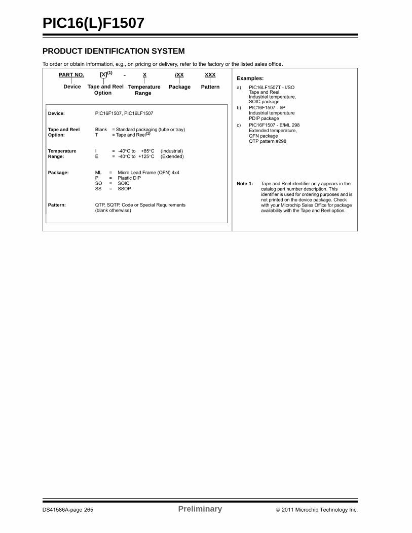
PIC16(L)F1507
DS41586A-page 265 Preliminary 2011 Microchip Technology Inc.
PRODUCT IDENTIFICATION SYSTEM
To order or obtain information, e.g., on pricing or delivery, refer to the factory or the listed sales office.
PART NO. X /XX XXX
PatternPackageTemperatureRange
Device
Device: PIC16F1507, PIC16LF1507
Tape and Reel Option:
Blank = Standard packaging (tube or tray) T = Tape and Reel(1)
Temperature Range:
I = -40C to +85C (Industrial)E = -40C to +125C (Extended)
Package: ML = Micro Lead Frame (QFN) 4x4P = Plastic DIPSO = SOICSS = SSOP
Pattern: QTP, SQTP, Code or Special Requirements (blank otherwise)
Examples:
a) PIC16LF1507T - I/SO Tape and Reel,Industrial temperature,SOIC package
b) PIC16F1507 - I/PIndustrial temperaturePDIP package
c) PIC16F1507 - E/ML 298Extended temperature,QFN packageQTP pattern #298
Note 1: Tape and Reel identifier only appears in the catalog part number description. This identifier is used for ordering purposes and is not printed on the device package. Check with your Microchip Sales Office for package availability with the Tape and Reel option.
[X](1)
Tape and ReelOption
-

DS41586A-page 266 Preliminary 2011 Microchip Technology Inc.
AMERICASCorporate Office2355 West Chandler Blvd.Chandler, AZ 85224-6199Tel: 480-792-7200 Fax: 480-792-7277Technical Support: http://www.microchip.com/supportWeb Address: www.microchip.com
AtlantaDuluth, GA Tel: 678-957-9614 Fax: 678-957-1455
BostonWestborough, MA Tel: 774-760-0087 Fax: 774-760-0088
ChicagoItasca, IL Tel: 630-285-0071 Fax: 630-285-0075
ClevelandIndependence, OH Tel: 216-447-0464 Fax: 216-447-0643
DallasAddison, TX Tel: 972-818-7423 Fax: 972-818-2924
DetroitFarmington Hills, MI Tel: 248-538-2250Fax: 248-538-2260
IndianapolisNoblesville, IN Tel: 317-773-8323Fax: 317-773-5453
Los AngelesMission Viejo, CA Tel: 949-462-9523 Fax: 949-462-9608
Santa ClaraSanta Clara, CA Tel: 408-961-6444Fax: 408-961-6445
TorontoMississauga, Ontario, CanadaTel: 905-673-0699 Fax: 905-673-6509
ASIA/PACIFICAsia Pacific OfficeSuites 3707-14, 37th FloorTower 6, The GatewayHarbour City, KowloonHong KongTel: 852-2401-1200Fax: 852-2401-3431
Australia - SydneyTel: 61-2-9868-6733Fax: 61-2-9868-6755
China - BeijingTel: 86-10-8569-7000 Fax: 86-10-8528-2104
China - ChengduTel: 86-28-8665-5511Fax: 86-28-8665-7889
China - ChongqingTel: 86-23-8980-9588Fax: 86-23-8980-9500
China - HangzhouTel: 86-571-2819-3180 Fax: 86-571-2819-3189
China - Hong Kong SARTel: 852-2401-1200 Fax: 852-2401-3431
China - NanjingTel: 86-25-8473-2460Fax: 86-25-8473-2470
China - QingdaoTel: 86-532-8502-7355Fax: 86-532-8502-7205
China - ShanghaiTel: 86-21-5407-5533 Fax: 86-21-5407-5066
China - ShenyangTel: 86-24-2334-2829Fax: 86-24-2334-2393
China - ShenzhenTel: 86-755-8203-2660 Fax: 86-755-8203-1760
China - WuhanTel: 86-27-5980-5300Fax: 86-27-5980-5118
China - XianTel: 86-29-8833-7252Fax: 86-29-8833-7256
China - XiamenTel: 86-592-2388138 Fax: 86-592-2388130
China - ZhuhaiTel: 86-756-3210040 Fax: 86-756-3210049
ASIA/PACIFICIndia - BangaloreTel: 91-80-3090-4444 Fax: 91-80-3090-4123
India - New DelhiTel: 91-11-4160-8631Fax: 91-11-4160-8632
India - PuneTel: 91-20-2566-1512Fax: 91-20-2566-1513
Japan - YokohamaTel: 81-45-471- 6166 Fax: 81-45-471-6122
Korea - DaeguTel: 82-53-744-4301Fax: 82-53-744-4302
Korea - SeoulTel: 82-2-554-7200Fax: 82-2-558-5932 or 82-2-558-5934
Malaysia - Kuala LumpurTel: 60-3-6201-9857Fax: 60-3-6201-9859
Malaysia - PenangTel: 60-4-227-8870Fax: 60-4-227-4068
Philippines - ManilaTel: 63-2-634-9065Fax: 63-2-634-9069
SingaporeTel: 65-6334-8870Fax: 65-6334-8850
Taiwan - Hsin ChuTel: 886-3-6578-300Fax: 886-3-6578-370
Taiwan - KaohsiungTel: 886-7-213-7830Fax: 886-7-330-9305
Taiwan - TaipeiTel: 886-2-2500-6610 Fax: 886-2-2508-0102
Thailand - BangkokTel: 66-2-694-1351Fax: 66-2-694-1350
EUROPEAustria - WelsTel: 43-7242-2244-39Fax: 43-7242-2244-393Denmark - CopenhagenTel: 45-4450-2828 Fax: 45-4485-2829
France - ParisTel: 33-1-69-53-63-20 Fax: 33-1-69-30-90-79
Germany - MunichTel: 49-89-627-144-0 Fax: 49-89-627-144-44
Italy - Milan Tel: 39-0331-742611 Fax: 39-0331-466781
Netherlands - DrunenTel: 31-416-690399 Fax: 31-416-690340
Spain - MadridTel: 34-91-708-08-90Fax: 34-91-708-08-91
UK - WokinghamTel: 44-118-921-5869Fax: 44-118-921-5820
Worldwide Sales and Service
05/02/11