Embed Size (px)
Citation preview
PIC MICROCONTROLLER BASED AUTOMATIC POWER FACTOR
CORRECTION USING SWITCHED SINGLE CAPACITOR
Md. Humayun Kabir Khan (Masum)
Department of Electrical and Electronic Engineering
Dhaka University of Engineering & Technology, Gazipur
January 2018
i
PIC MICROCONTROLLER BASED AUTOMATIC POWER FACTOR
CORRECTION USING SWITCHED SINGLE CAPACITOR
A dissertation submitted in partial fulfillment of the requirements for the degree of
Master of Engineering in Electrical and Electronic Engineering
By
Md. Humayun Kabir Khan (Masum)
Student No. 112250-P
Under Supervision of
Dr. Md. Raju Ahmed Professor, Dept. of EEE
Department of Electrical and Electronic Engineering
Dhaka University of Engineering & Technology, Gazipur
January 2018

ii
The project titled “PIC microcontroller based automatic power factor correction using
switched single capacitor” submitted by Mr. Md. Humayun Kabir Khan (Masum), Student ID: 112250-P has been accepted as satisfactory in partial fulfillment of requirement for the degree of
Master of Engineering in Electrical and Electronic Engineering on 11th January, 2018. Boards of Examiners
…………………………………….. Dr. Md. Raju Ahmed Professor and Head of the Department, Department of Electrical and Electronic Engineering, Dhaka University of Engineering & Technology, Gazipur
Chairman (Supervisor) (Ex-officio)
…………………………………….. Dr. Md. Bashir Uddin Professor, Department of Electrical and Electronic Engineering, Dhaka University of Engineering & Technology, Gazipur
Member
…………………………………….. Dr. Md. Anwarul Abedin Professor, Department of Electrical and Electronic Engineering, Dhaka University of Engineering & Technology, Gazipur
Member
…………………………………….. Dr. Ruma Professor, Department of Electrical and Electronic Engineering, Dhaka University of Engineering & Technology, Gazipur
Member
…………………………………….. Dr. Md. Aynal Haque Professor, Department of Electrical and Electronic Engineering, Bangladesh University of Engineering & Technology, Dhaka
Member (External)

iii
Declaration I declare that this project is my own work and has not been submitted in any form for
another degree or diploma at any university or other institute of tertiary education.
Information derived from the published and unpublished work of others has been
acknowledged in the text and a list of references is given.
Md. Humayun Kabir Khan (Masum) Date: 11/1/2018

iv
Acknowledgement
First of all, I thank the Almighty, who gave me the opportunity and strength to carry out
this research work.
I would like to express my sincere gratitude and profound indebtedness to my supervisor
and Head, Department of EEE, Dhaka University of Engineering & Technology, Gazipur
Dr. Md. Raju Ahmed for constant guidance, insightful advice, helpful criticism, valuable
suggestions, commendable support and endless patience towards the completion of this
project. I feel very proud to have worked with him. Without his inspiring enthusiasm and
encouragement, this work could not have been completed.
I thank all my teachers and staffs at the Department of EEE, Dhaka University of
Engineering & Technology for their support and encouragement.
I wish to express my gratitude to Dhaka University of Engineering & Technology, Gazipur
for providing an excellent environment for research. The support I have received from
Dhaka University of Engineering & Technology is gratefully acknowledged.
I would like to express my most sincere gratitude to my family, my friends and well
wishers who are taking lot of pains for progress in my life and for their sacrifices, blessings
and constant prayers for my advancement.
Finally, last but not least, I am also thankful to those, who have directly or indirectly helped
me and encouraged me to complete my project. I feel sorry for not able to express my
appreciation to each of my well-wishers and ask forgiveness for my improper behavior with
anyone who was intending to help me.
v
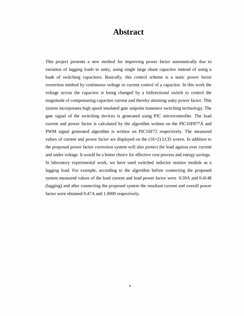
Abstract This project presents a new method for improving power factor automatically due to
variation of lagging loads to unity, using single large shunt capacitor instead of using a
bank of switching capacitors. Basically, this control scheme is a static power factor
correction method by continuous voltage or current control of a capacitor. In this work the
voltage across the capacitor is being changed by a bidirectional switch to control the
magnitude of compensating capacitor current and thereby attaining unity power factor. This
system incorporates high speed insulated gate unipolar transistor switching technology. The
gate signal of the switching devices is generated using PIC microcontroller. The load
current and power factor is calculated by the algorithm written on the PIC16F877A and
PWM signal generated algorithm is written on PIC16F72 respectively. The measured
values of current and power factor are displayed on the (16×2) LCD screen. In addition to
the proposed power factor correction system will also protect the load against over current
and under voltage. It would be a better choice for effective cost process and energy savings.
In laboratory experimental work, we have used switched inductor resistor module as a
lagging load. For example, according to the algorithm before connecting the proposed
system measured values of the load current and load power factor were 0.59A and 0.4148
(lagging) and after connecting the proposed system the resultant current and overall power
factor were obtained 0.47A and 1.0000 respectively.
vi
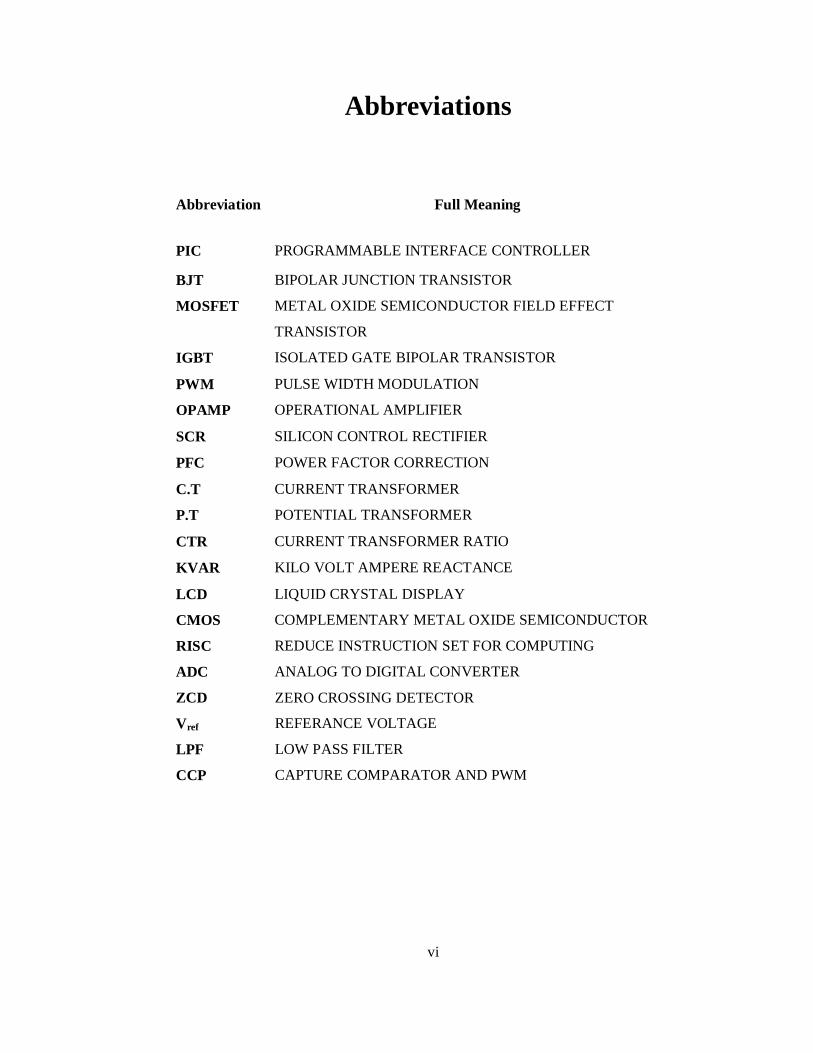
Abbreviations
Abbreviation Full Meaning
PIC PROGRAMMABLE INTERFACE CONTROLLER
BJT BIPOLAR JUNCTION TRANSISTOR
MOSFET METAL OXIDE SEMICONDUCTOR FIELD EFFECT
TRANSISTOR
IGBT ISOLATED GATE BIPOLAR TRANSISTOR
PWM PULSE WIDTH MODULATION
OPAMP OPERATIONAL AMPLIFIER
SCR SILICON CONTROL RECTIFIER
PFC POWER FACTOR CORRECTION
C.T CURRENT TRANSFORMER
P.T POTENTIAL TRANSFORMER
CTR CURRENT TRANSFORMER RATIO
KVAR KILO VOLT AMPERE REACTANCE
LCD LIQUID CRYSTAL DISPLAY
CMOS COMPLEMENTARY METAL OXIDE SEMICONDUCTOR
RISC REDUCE INSTRUCTION SET FOR COMPUTING
ADC ANALOG TO DIGITAL CONVERTER
ZCD ZERO CROSSING DETECTOR
Vref REFERANCE VOLTAGE
LPF LOW PASS FILTER
CCP CAPTURE COMPARATOR AND PWM

vii
List of Contents Page No Declaration iii Acknowledgement iv Abstract v Abbreviations vi List of Figures ix List of Tables xi Chapter 1: Introduction 1.1 Introduction 1 1.2 Literature Review 2 1.3 Specific Aims of the Project 5 1.4 Project Report Organization 5 Chapter 2: Design and Simulation of the Proposed Power Factor Correction Circuit 2.1 Introduction 6 2.2 Block Diagram Overview of the Project 6 2.3 Power Supply Unit 8 2.4 Precision Rectifier Circuit 8 2.5 Zero Crossing Detectors 9 2.6 Switched Single Capacitor 10 2.7 IGBT/ Power MOSFET Isolated Gate Drive 11 2.8 AC to AC Buck Converter 12 2.9 LC Low Pass Filter 13 2.10 Current and Power Factor Measurement 15 2.11 PWM Signal Generation 18 Chapter 3: Implementation of the Proposed Power Factor Correction Circuit 3.1 Introduction 24 3.2 PIC16F877A 40-Pin Enhanced Flash Microcontroller 24 3.3 PIC16F72 28-Pin Enhanced Flash Microcontroller 27 3.4 Regulated IC L7805CV 29 3.5 Capacitor 31 3.6 NPN Silicon Transistors (BC547N) 32 3.7 PNP Silicon Transistor (BC557) 32
viii
3.8 Power MOSFET (IRFP460) 33 3.9 Power IGBT (IXGH10N60A) 33 3.10 Opto-Coupler (4N25) 34 3.11 Liquid Crystal Display (HD44780) 35 3.12 Crystal Oscillator 37 3.13 Op-amp (LM358 and LM324N) 37
3.14 Precision Current Sensor (TA1309-100) 38 3.15 Experimental Setup 39 3.16 Experimental Results 43
Chapter 4: Conclusion and Recommendation 4.1 Conclusion 48 4.2 Recommendation for future work 48 REFFERENCES 49 APPENDIX 51
ix
List of Figures
Page No
Figure 2.1 Starting of PROTEUS software for designing electronic circuits. 6 Figure 2.2 Block diagram of proposed power factor correction system. 7 Figure 2.3 Power supply unit for microcontroller and precision rectifier. 8 Figure 2.4 Precision half-wave AC/DC converter. 9 Figure 2.5 Sine to square wave converters. 10 Figure 2.6 Output of the zero crossing detectors. 10 Figure 2.7 Isolated power supply unit. 11 Figure 2.8 Opto isolated gate driver circuit. 12 Figure 2.9 Controlling an AC load with a power MOSFET 12 Figure 2.10 LPF output voltage level after filtering. 13 Figure 2.11 LC Pi and T section low pass filters. 14 Figure 2.12 Switch single capacitor with T section low pass filter. 14 Figure 2.13 Circuit diagram for current and power factor measurement. 15 Figure 2.14 Flow chart diagram for current and power factor measurement. 16 Figure 2.15 Proteus simulation result without load. 17 Figure 2.16 Proteus simulation result with one (50+j63) Ω load. 17 Figure 2.17 Circuit diagram for PWM signal generation. 18 Figure 2.18 Flow chart diagram for PWM signal generation. 19 Figure 2.19 Proteus simulation circuit for measurement of both input voltage and
current. 20
Figure 2.20 No PWM signal without load. 20 Figure 2.21 V& I waveforms with one (50+j63) inductive load. 21 Figure 2.22 PWM signal is produced by μc to attained unity power factor. 21 Figure 2.23 Circuit Input V-I waveforms 21 Figure 2.24 Voltage across the shunt capacitor (100uF) was 123.16V (peak) 21 Figure 2.25 V& I waveforms with three (50+j79) inductive loads. 22 Figure 2.26 PWM signal is produced by μc to attained unity power factor for three
(50+j79) inductive loads. 22
Figure 2.27 Circuit Input V-I waveforms 22 Figure 2.28 Voltage across the shunt capacitor (100uf) was 302.69V (peak). 22 Figure 2.29 V& I waveforms with one (50+j47) inductive load. 23 Figure 2.30 PWM signal is produced by μc to attained unity power factor for one
(50+j47) inductive load. 23
Figure 2.31 Circuit Input V-I waveforms. 23 Figure 2.32 Voltage across the shunt capacitor (100uf) was 126.69V (peak). 23 Figure 3.1 Block diagram of PIC 16F877A microcontroller. 26 Figure 3.2 Pin configuration of PIC 16F877A microcontroller. 27 Figure 3.3 Block diagram of PIC 16F72 microcontroller. 28 Figure 3.4 Pin diagram of PIC16F72 microcontroller. 28 Figure 3.5 L7805CV +5V linear voltage regulator. 31 Figure 3.6 A ceramic capacitor and an electrolyte capacitor respectively. 31 Figure 3.7 Typical BC547N silicon transistor. 32
x
Figure 3.8 Typical BC557 silicon transistor. 32 Figure 3.9 IRFP460 terminal pin configuration. 33 Figure 3.10 IXGH10N60A terminal pin configuration. 33 Figure 3.11 Internal structure of an opto-coupler. 34 Figure 3.12 Pin configuration of 4N25 opto-coupler. 35 Figure 3.13 HD44780 liquid crystal display (LCD). 36 Figure 3.14 A typical 16MHz crystal oscillator. 37 Figure 3.15 Pin configurations of LM358 and LM324N respectively. 38 Figure 3.16 Welding pins and typical connection diagram of TA1309-100/200
sensor. 38
Figure 3.17 Circuit implementation of the proposed circuit. 39 Figure 3.18 Practically implemented proposed project in working mode. 40 Figure 3.19 Different components of the current and power factor measurement
circuit. 40
Figure 3.20 PWM signal generation circuit. 41 Figure 3.21 IGBT gate driver circuit. 41 Figure 3.22 Implemented power supply circuit 42 Figure 3.23 Power IGBT and Heavy (10 to 50A) metal rectifier bridge circuit. 42 Figure 3.24 Switched single capacitor with low pass filter circuit; where
L1=5.6mH, L2=5.6mH, C1=2uF and single capacitor =10uF. 42
Figure 3.25 Output square voltage waveform from IC LM324N zero crossing detectors, when input frequency 50Hz (Sine).
43
Figure 3.26 Output waveform of voltage and current zero crossing detectors respectively, when input frequency 50Hz (Sine) but no-load was connected with the system.
43
Figure 3.27 Output voltage waveforms of ZCD-V and ZCD-I, when only one soldering iron (25W, 220V, 50Hz AC) has been connected with the system.
43
Figure 3.28 Output voltage waveforms of ZCD-V and ZCD-I respectively, when one small inductive load has been connected with the system (Tdiff. = 3ms).
44
Figure 3.29 Waveform of PWM signal, when load current and power factor were 0.56A and 0.9601 lagging respectively.
44
Figure 3.30 Voltage waveform across the switched single capacitor after low pass filtering, when load power factor and current were 0.7293 lagging and 0.47A respectively.
44
Figure 3.31 Experimental setup of the proposed project in laboratory. 45 Figure 3.32 No load was connected with the system. 45 Figure 3.33 Real-time results, (a) without switched single capacitor (displayed
load current and load power factor), (b) after connecting switched single capacitor across the load(s) (displayed resultant current/ circuit input current and overall power factor).
46

xi
List of Tables
Page No Table I Input and output characteristic data of TA1309-100 precision current
sensor. 38
Table II Laboratory experimental results before and after power factor correction. 47
1
Chapter 1
Introduction 1.1 Introduction Static power compensation is becoming one of the most economic and effective solution to
both traditional and new problems in power transmission system. It is a well-established
practice to use reactive power compensation to control the magnitude of the voltage at a
particular bus bar in electric power system. In the past, synchronous condensers,
mechanically switched capacitors and saturated reactors have been applied to control the
system voltage. Since the late 1960s, thyristor controlled reactor (TCR) devices together
with fixed capacitors (FCs) or thyristor switched capacitors (TSCS) have been used to
inject or absorb reactive power. Solid state VAR compensators using force-commutated
converters and based on force-commutated voltage source have been recently discussed. In
an ideal electrical system, the voltage and frequency in the various points of power
distribution must be constant, presenting only the fundamental component and a near unity
power factor.
In particular, these parameters must be independent of the size and characteristics of the
loads; this can be obtained only if these loads are equipped with reactive power
compensators to make the network independent from probable changes that appear in the
distribution points. Compensation of the load is one of techniques for the controlling of
reactive power so to improve the quality of the energy in the ac transmission lines. This
technique is generally used for the compensation of individual or a group of loads. Power
factor correction is the capability of generating or absorbing reactive power to a load
without the use of the supply power. The major industrial loads are inductive; hence the
current tends to go beyond the necessary value to active power absorption alone. But active
power is usually used for the power conversion, and an excessive load current represents a
loss for the consumer, who not only pays for the over dimensioning of the cable but also for
the excessive power loss in the cables. The electric companies do not want to transport the
useless reactive power of the alternators towards the loads, the distribution network cannot
2
be used at high efficiency and the voltage regulation in the various points becomes
complicated. The pricing used by these electric companies almost always penalizes the low
power factor of the clients; hence the development of systems for power factor
improvement is necessary. In traditional power factor improvement unit, a number of
capacitor is used in parallel which is connected to the load through magnetic contactor
[1]-[3]. Depending on the required KVAR, a number of capacitor is connected to the load
by microcontroller using the magnetic contractor. Therefore, power factor is corrected step
by step [4], it is not always maintained the unity power factor. In this case expensive
magnetic contractor is required to connect the capacitors. Problem in magnetic contractor is
frequently observed. In the proposed circuit, capacitor (single large capacitor or a number
of capacitor connected in parallel works as single capacitor) will always connect to the load
and the voltage across the capacitor will be changed to control the compensating current.
Therefore the expensive magnetic contactor can be omitted and power factor can be
controlled sleeplessly to unity. Consequently the proposed circuit will be robust and more
cost effective. The proposed circuit will incorporate the facility to monitor the load current,
voltage, power factor, compensating capacitive current and protection of load against over
current and under-voltage variation.
1.2 Literature Review Though correction of power factor is very old practice, many of the authors below have
suggested and prescribe many ways of power factor correction.
Oommen and Kohler [5] explored the advantages that can be accomplished by proper
implementation of power factor compensation. Different compensators along with the
sizing and strategic location was also considered. A brief study on the economic analysis
was carried out to show the economic viability of compensation.
Jiang et al. [6] proposed a novel single-phase power factor correction scheme based on
parallel power factor correction concept which was described to be more efficient than
convention two-cascade stage scheme.
3
Qureshi and Aslam [7] outlined the different methods for power factor correction and
carried out an experimental case study to explore the areas which will be suitable for
compensation. After a practical demonstration to have a significant improvement in power
factor was completed, they found that it would release the capacity of distribution
transformer and the problem of over voltage under condition of low load was avoided.
Novak and Kohler [8] pointed out the importance of power factor improvement for
technological innovation and advancement in deep coal mine power systems. Different
protection equipment to check the inherent electrical faults in the mining system were
argued. The power factor correction near loads for improved voltage regulation was
emphasized within the constraints of high voltage distribution in underground coal mines.
Shwehdi and Sultan [9] suggested some mathematical calculations for power factor and
reactive power requirement of the system along with the capacitor size estimation methods.
Celtekligil [10] discussed the application of a method for dynamic power factor correction
and voltage regulation in light rail transportation system. Main reactors have been switched
on through thyristors using automatic power controllers by sensing the power factor and
constantly monitoring the current and voltage, calculating the power factor and switching
inductance banks as required. The system is proposed connects inductive loads in parallel
with the capacitive system to improve the power factor.
Choudhury [11] gave a design and implementation of a low cost power factor
improvement device for small signal low power loads. The design was involved designing
of a small signal model load, selecting appropriate capacitors, and designing appropriate
switching circuits to select proper combination of capacitors.
Shahid and Anwar [12] offered the design of a power factor improvement circuit using
PIC with reduced parts count to achieve desired efficiency and low cost. The solution
involves ensuring the power factor value from the load and uses an algorithm to determine
and trigger switching capacitors in order to compensate for excessive reactive components
to increase power factor value.

4
Sharma and Haque [13] carried out a simulation and analysis study for power factor
correction for metal halide high intensity discharge lamps. A modified boost converter
using active devices was proposed along with PI controller to stabilize the control loops.
Allah [14] suggested an automatic power factor correction based on Alienation technique.
An alienation technique was developed for calculation of original power factor on-line,
active and compensation reactive powers and determination of the required number of
capacitor banks to get the desired power factor. Alienation coefficients were calculated
between phase voltage and current signals of power supply. Alternative transient program
(ATP) and MATLAB programs were used to implement the proposed technique.
According to above discussion, we have found that some authors avoided the problem of
over voltage during low load. Some authors suggested only mathematical calculations and
software simulation for estimating the capacitor size. Some systems were proposed by
connecting inductive loads in parallel with the capacitive system to improve the power
factor through high power rating TCR and some system were designed and implemented
for small signal low power load. On the other hand, in traditional power factor
improvement unit, a number of capacitors are used in parallel which are connected to the
load through magnetic contactors and detuned reactors. Due to switching effect, sparking
occurs in the magnetic contactors for frequently changing connected loads, as a result
excessive heat burns the magnetic contactors. Basically traditional system is fruitful for
balanced three phase load and power factor is corrected step by step. For this, both the
traditional and suggested system will have to be improved.

5
1.3 Specific Aims of the Project
Reactive power compensation or control is essential part in a power system to minimize
power transmission loss, to maximize power transmission capability and to maintain the
system voltage within desired level.
The specific issues that will be analyzed in this project can be summarized as follows:
a) To design and implement a PFC unit, which improves the power factor
automatically of varying lagging loads to unity using pulse width modulated
switched capacitor.
b) To measure and display the values of load current, power factor, capacitive
current, circuit input current and overall power factor in the LCD display.
c) To design a system to protect the load against over current and under-
voltage.
1.4 Project Report Organization
This report consists of four chapters.
Chapter 1 Gives brief discussion of the project introduction, project review and project
objectives.
Chapter 2 Focuses on the design and simulation results of the proposed PFC system.
Chapter 3 Focuses on the system implementation and explains the results of the system
development of this project, and it also contains the accessories of controlling system based
on the research conducted towards the development of the project. The theoretical reviews
covered are Microcontroller PIC 16F877A and PIC16F72, IGBT, N-MOSFET, BJT,
Regulated Power IC LM7805 and LM7905, Opto-coupler, Precision C.T, P.T, Op-amp
LM324N and LM358, Fast Switching Bridge Rectifier, Crystal and 16×2 LCD.
Chapter 4 Concludes overall discussion of proposed project and future recommendations
are also presented in this chapter.

6
Chapter 2
Design and Simulation of the Proposed Power Factor Correction Circuit
2.1 Introduction In this chapter, the proposed PIC microcontroller based automatic power factor correction
circuit is designed and analyzed using simulation software before implementation.
PROTEUS software, version 7.5 which is circuit simulation software is used for the present
analysis. The proposed circuit is designed step by step, starting from power supply unit and
finally designed the complete proposed project. The starting of PROTEUS software for
designing and analysis of electrical and electronic circuits is shown in Figure 2.1[15].
Figure 2.1: Starting of PROTEUS software for designing circuits. 2.2 Block Diagram of the Proposed System The wide range of variation in lagging VAR on the system has caused the necessity for
controlled compensation of the reactive power to achieve desired power factor at all load
conditions. This is usually achieved by using switched capacitors. Depending on the total
VAR requirement, a number of capacitors are used which can be switched into or switched
outgo the system individually. But in case of widely fluctuating loads, the VAR of the load
also varies over wide limits. Thus a fixed capacitor bank may often lead to either
overcompensation or under-compensation resulting in lower power factor in the AC power
supply system. In this research instead of using a bank of capacitor a single large capacitor
(or a number of capacitor connected in parallel works as a single capacitor) is used. The
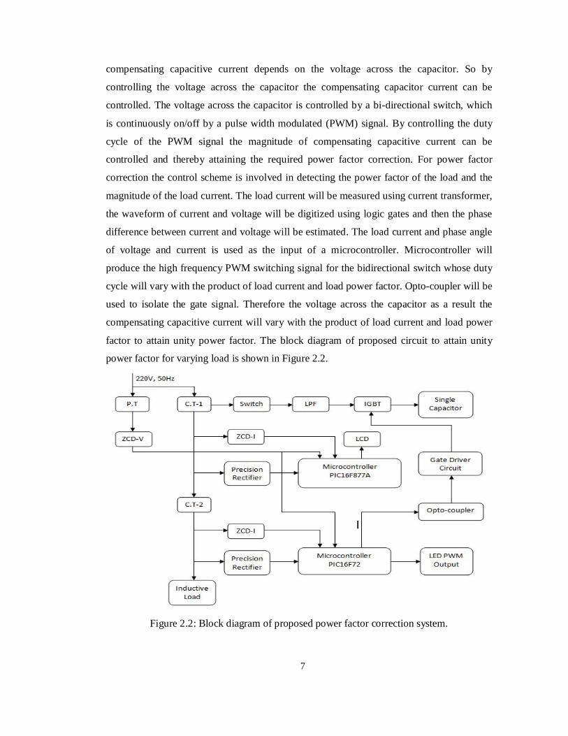
7
compensating capacitive current depends on the voltage across the capacitor. So by
controlling the voltage across the capacitor the compensating capacitor current can be
controlled. The voltage across the capacitor is controlled by a bi-directional switch, which
is continuously on/off by a pulse width modulated (PWM) signal. By controlling the duty
cycle of the PWM signal the magnitude of compensating capacitive current can be
controlled and thereby attaining the required power factor correction. For power factor
correction the control scheme is involved in detecting the power factor of the load and the
magnitude of the load current. The load current will be measured using current transformer,
the waveform of current and voltage will be digitized using logic gates and then the phase
difference between current and voltage will be estimated. The load current and phase angle
of voltage and current is used as the input of a microcontroller. Microcontroller will
produce the high frequency PWM switching signal for the bidirectional switch whose duty
cycle will vary with the product of load current and load power factor. Opto-coupler will be
used to isolate the gate signal. Therefore the voltage across the capacitor as a result the
compensating capacitive current will vary with the product of load current and load power
factor to attain unity power factor. The block diagram of proposed circuit to attain unity
power factor for varying load is shown in Figure 2.2.
Figure 2.2: Block diagram of proposed power factor correction system.

8
After simulating the proposed power factor improvement unit using simulation software,
the circuit will be implemented practically in laboratory. The implemented circuit will be
verified for different value of load current and load power factor. LCD will be displayed the
load current, voltage, power factor, compensating capacitive current etc. Load current,
voltage and the frequency of the supply will be also measured and compared with the set
value of load current, voltage and frequency using microcontroller. If there is over current
or under voltage variation microcontroller will disconnect the load from supply using relay
to protect the load and improve the stability of the system.
2.3 Power Supply Unit
Figure 2.3: Power supply unit for microcontroller and precision rectifier.
The PIC16F877A and PIC16F72 microcontrollers can operate at different supply voltages.
A +5V DC power supply is the most suitable. The circuit diagram is shown in Figure 2.3
uses a cheap integrated three-terminal positive regulator LM7805 and provides high-quality
voltage stability and quite enough current to enable the microcontroller and peripheral
component to operate normally (enough here means 1A). Also LM7905 provides negative
stable voltage (-5V) for precision rectifier circuit.
2.4 Precision Rectifier Circuit Rectifier circuits are used in the design of power supply circuits. In such applications, the
voltage being rectified is usually much greater than the diode voltage drop, rendering the
exact value of the diode drop unimportant to the proper operation of the rectifier. Other
application exists, however, where this is not the case. For example, in instrumentation
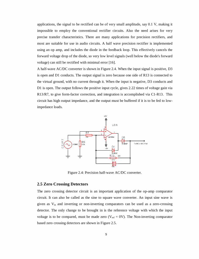
9
applications, the signal to be rectified can be of very small amplitude, say 0.1 V, making it
impossible to employ the conventional rectifier circuits. Also the need arises for very
precise transfer characteristics. There are many applications for precision rectifiers, and
most are suitable for use in audio circuits. A half wave precision rectifier is implemented
using an op amp, and includes the diode in the feedback loop. This effectively cancels the
forward voltage drop of the diode, so very low level signals (well below the diode's forward
voltage) can still be rectified with minimal error [16].
A half-wave AC/DC converter is shown in Figure 2.4. When the input signal is positive, D3
is open and D1 conducts. The output signal is zero because one side of R13 is connected to
the virtual ground, with no current through it. When the input is negative, D3 conducts and
D1 is open. The output follows the positive input cycle, gives 2.22 times of voltage gain via
R13/R7, to give form-factor correction, and integration is accomplished via C1-R13. This
circuit has high output impedance, and the output must be buffered if it is to be fed to low-
impedance loads.
Figure 2.4: Precision half-wave AC/DC converter.
2.5 Zero Crossing Detectors The zero crossing detector circuit is an important application of the op-amp comparator
circuit. It can also be called as the sine to square wave converter. An input sine wave is
given as Vin and inverting or non-inverting comparators can be used as a zero-crossing
detector. The only change to be brought in is the reference voltage with which the input
voltage is to be compared, must be made zero (Vref = 0V). The Non-inverting comparator
based zero crossing detectors are shown in Figure 2.5.
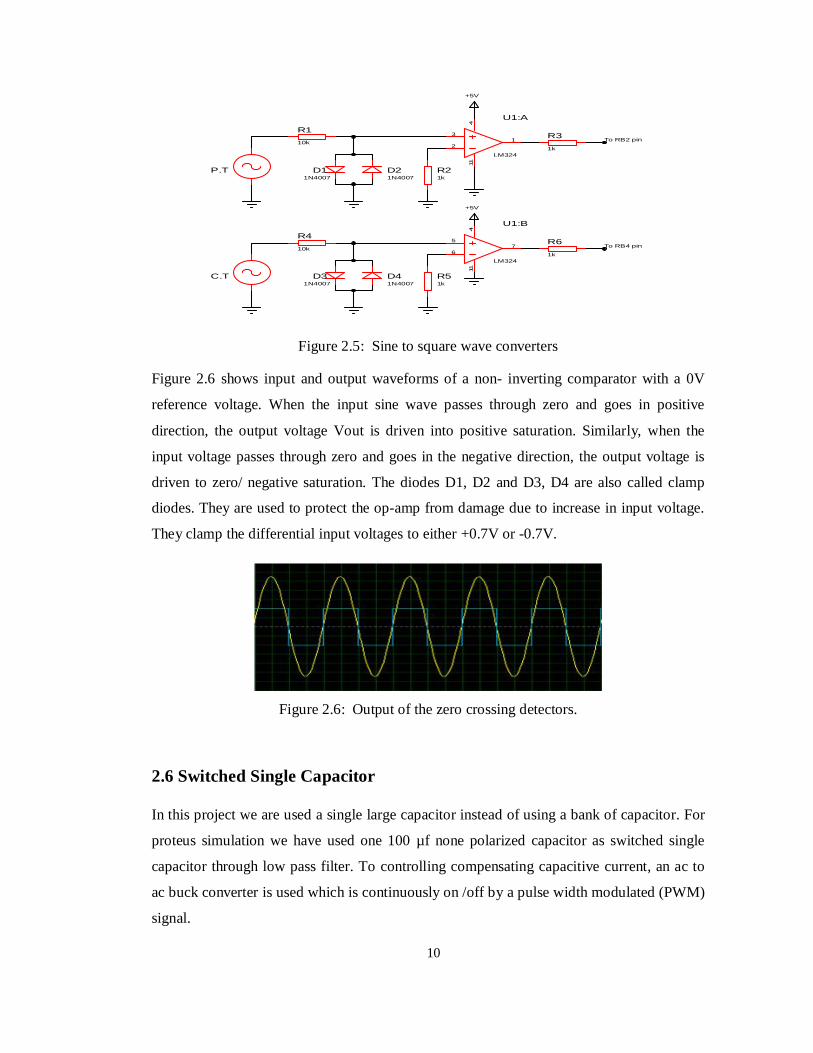
10
3
21
411
U1:A
LM324
R110k
D11N4007
D21N4007
R21k
P.T
+5V
R3
1k
To RB2 pin
5
67
411
U1:B
LM324
R4
10k
D31N4007
D41N4007
R51k
C.T
+5V
R6
1k
To RB4 pin
Figure 2.5: Sine to square wave converters
Figure 2.6 shows input and output waveforms of a non- inverting comparator with a 0V
reference voltage. When the input sine wave passes through zero and goes in positive
direction, the output voltage Vout is driven into positive saturation. Similarly, when the
input voltage passes through zero and goes in the negative direction, the output voltage is
driven to zero/ negative saturation. The diodes D1, D2 and D3, D4 are also called clamp
diodes. They are used to protect the op-amp from damage due to increase in input voltage.
They clamp the differential input voltages to either +0.7V or -0.7V.
Figure 2.6: Output of the zero crossing detectors.
2.6 Switched Single Capacitor In this project we are used a single large capacitor instead of using a bank of capacitor. For
proteus simulation we have used one 100 µf none polarized capacitor as switched single
capacitor through low pass filter. To controlling compensating capacitive current, an ac to
ac buck converter is used which is continuously on /off by a pulse width modulated (PWM)
signal.
11
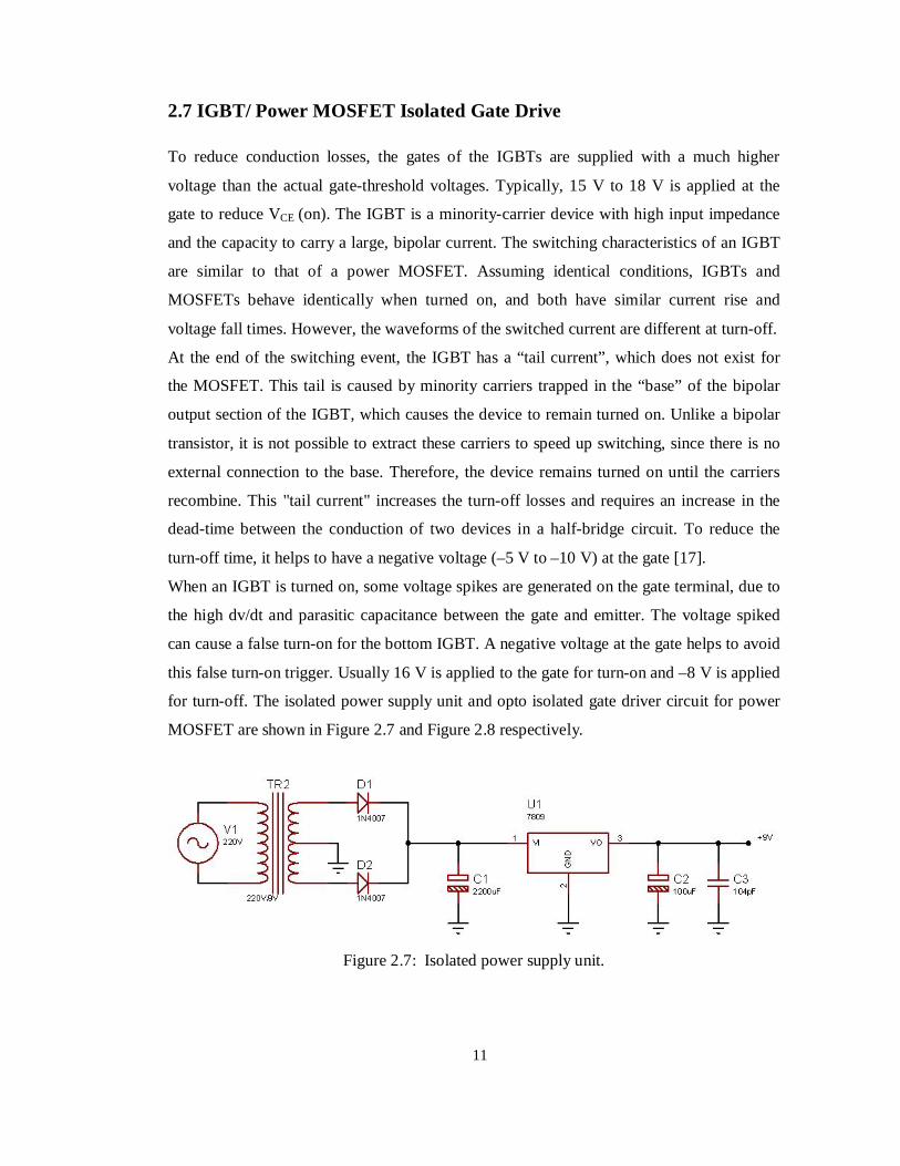
2.7 IGBT/ Power MOSFET Isolated Gate Drive
To reduce conduction losses, the gates of the IGBTs are supplied with a much higher
voltage than the actual gate-threshold voltages. Typically, 15 V to 18 V is applied at the
gate to reduce VCE (on). The IGBT is a minority-carrier device with high input impedance
and the capacity to carry a large, bipolar current. The switching characteristics of an IGBT
are similar to that of a power MOSFET. Assuming identical conditions, IGBTs and
MOSFETs behave identically when turned on, and both have similar current rise and
voltage fall times. However, the waveforms of the switched current are different at turn-off.
At the end of the switching event, the IGBT has a “tail current”, which does not exist for
the MOSFET. This tail is caused by minority carriers trapped in the “base” of the bipolar
output section of the IGBT, which causes the device to remain turned on. Unlike a bipolar
transistor, it is not possible to extract these carriers to speed up switching, since there is no
external connection to the base. Therefore, the device remains turned on until the carriers
recombine. This "tail current" increases the turn-off losses and requires an increase in the
dead-time between the conduction of two devices in a half-bridge circuit. To reduce the
turn-off time, it helps to have a negative voltage (–5 V to –10 V) at the gate [17].
When an IGBT is turned on, some voltage spikes are generated on the gate terminal, due to
the high dv/dt and parasitic capacitance between the gate and emitter. The voltage spiked
can cause a false turn-on for the bottom IGBT. A negative voltage at the gate helps to avoid
this false turn-on trigger. Usually 16 V is applied to the gate for turn-on and –8 V is applied
for turn-off. The isolated power supply unit and opto isolated gate driver circuit for power
MOSFET are shown in Figure 2.7 and Figure 2.8 respectively.
Figure 2.7: Isolated power supply unit.
12
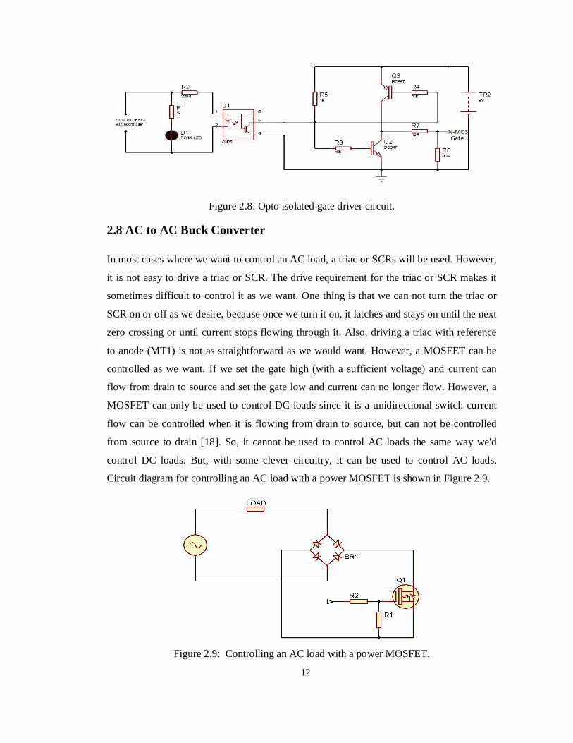
Figure 2.8: Opto isolated gate driver circuit.
2.8 AC to AC Buck Converter
In most cases where we want to control an AC load, a triac or SCRs will be used. However,
it is not easy to drive a triac or SCR. The drive requirement for the triac or SCR makes it
sometimes difficult to control it as we want. One thing is that we can not turn the triac or
SCR on or off as we desire, because once we turn it on, it latches and stays on until the next
zero crossing or until current stops flowing through it. Also, driving a triac with reference
to anode (MT1) is not as straightforward as we would want. However, a MOSFET can be
controlled as we want. If we set the gate high (with a sufficient voltage) and current can
flow from drain to source and set the gate low and current can no longer flow. However, a
MOSFET can only be used to control DC loads since it is a unidirectional switch current
flow can be controlled when it is flowing from drain to source, but can not be controlled
from source to drain [18]. So, it cannot be used to control AC loads the same way we'd
control DC loads. But, with some clever circuitry, it can be used to control AC loads.
Circuit diagram for controlling an AC load with a power MOSFET is shown in Figure 2.9.
Figure 2.9: Controlling an AC load with a power MOSFET.
13
As we can see, due to the bridge rectifier, the MOSFET always "sees" a DC voltage as the
drain is always positive with respect to the source. Thus, with this combination of the
bridge rectifier and MOSFET, by controlling a DC switch the MOSFET, we can control the
AC current flow and frequency of operation is 4 kHz, a normal bridge rectifier can not be
used. For the bridge rectifier, ultrafast diodes must be used. In a DC-DC buck converter, the
output voltage is given by; Vout = Vin × Duty Cycle. So, if duty cycle is 50% or 0.5, the
output voltage is half the input voltage. That is also correct for AC-AC buck converter.
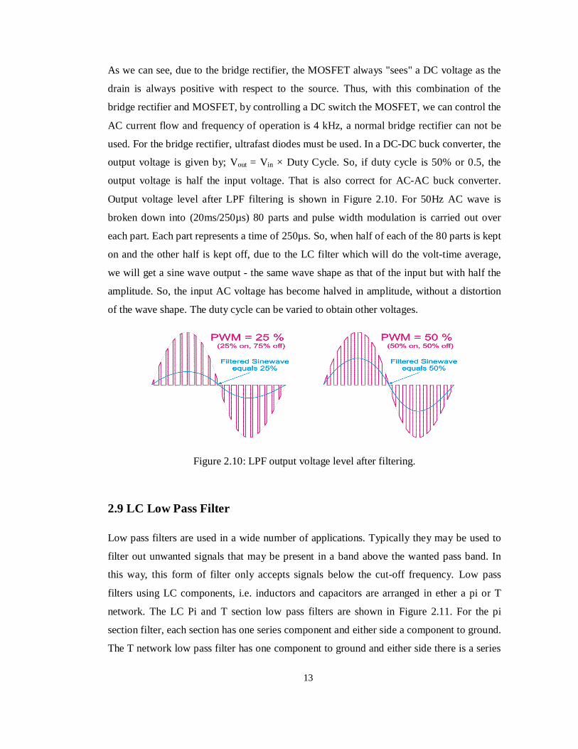
Output voltage level after LPF filtering is shown in Figure 2.10. For 50Hz AC wave is
broken down into (20ms/250µs) 80 parts and pulse width modulation is carried out over
each part. Each part represents a time of 250µs. So, when half of each of the 80 parts is kept
on and the other half is kept off, due to the LC filter which will do the volt-time average,
we will get a sine wave output - the same wave shape as that of the input but with half the
amplitude. So, the input AC voltage has become halved in amplitude, without a distortion
of the wave shape. The duty cycle can be varied to obtain other voltages.
Figure 2.10: LPF output voltage level after filtering.
2.9 LC Low Pass Filter
Low pass filters are used in a wide number of applications. Typically they may be used to
filter out unwanted signals that may be present in a band above the wanted pass band. In
this way, this form of filter only accepts signals below the cut-off frequency. Low pass
filters using LC components, i.e. inductors and capacitors are arranged in ether a pi or T
network. The LC Pi and T section low pass filters are shown in Figure 2.11. For the pi
section filter, each section has one series component and either side a component to ground.
The T network low pass filter has one component to ground and either side there is a series
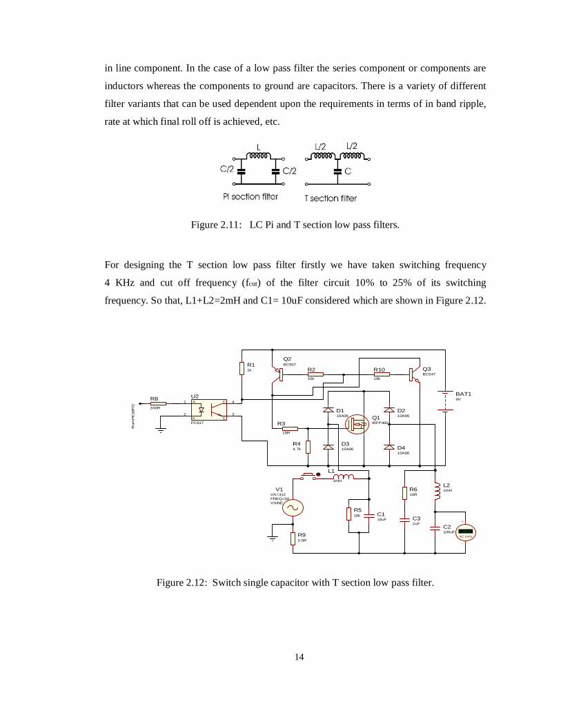
14
in line component. In the case of a low pass filter the series component or components are
inductors whereas the components to ground are capacitors. There is a variety of different
filter variants that can be used dependent upon the requirements in terms of in band ripple,
rate at which final roll off is achieved, etc.
Figure 2.11: LC Pi and T section low pass filters.
For designing the T section low pass filter firstly we have taken switching frequency
4 KHz and cut off frequency (fcut) of the filter circuit 10% to 25% of its switching
frequency. So that, L1+L2=2mH and C1= 10uF considered which are shown in Figure 2.12.
R8
330R D110A06
D210A06
D310A06 D4
10A06
Q1IRFP460
BAT19V
Q2BC557R1
1k R210k
R3
10R
R44.7k
L1
1mH
A
K
C
E
1
2
4
3
U2
PC817
L21mH
C110uF
V1
VSINE
VA=312FREQ=50
R510k
C2100uF
R610R
C32uF
R90.5R
+88.8AC Volts
Q3BC547
R1010k
From
PIC
16F7
2
Figure 2.12: Switch single capacitor with T section low pass filter.
15
2.10 Current and Power Factor Measurement
ACVSINEVA=312FREQ=50TD=0ms
RA0/AN02
RA1/AN13
RA2/AN2/VREF-/CVREF4
RA4/T0CKI/C1OUT6
RA5/AN4/SS/C2OUT7
RE0/AN5/RD8
RE1/AN6/WR9
RE2/AN7/CS10
OSC1/CLKIN13
OSC2/CLKOUT14
RC1/T1OSI/CCP2 16
RC2/CCP1 17
RC3/SCK/SCL 18
RD0/PSP0 19
RD1/PSP1 20
RB7/PGD 40RB6/PGC 39RB5 38RB4 37RB3/PGM 36RB2 35RB1 34
RB0/INT 33
RD7/PSP7 30RD6/PSP6 29RD5/PSP5 28RD4/PSP4 27RD3/PSP3 22RD2/PSP2 21
RC7/RX/DT 26RC6/TX/CK 25RC5/SDO 24RC4/SDI/SDA 23
RA3/AN3/VREF+5
RC0/T1OSO/T1CKI 15
MCLR/Vpp/THV1
U1
PIC16F877ACLOCK=20MHz
D7
14D
613
D5
12D
411
D3
10D
29
D1
8D
07
E6
RW5
RS
4
VSS
1
VD
D2
VEE
3
LCD1LM016L
L2
3.65H
R10353R
C.T
1:2000M=1
R8
10k
R11
10k
R12
1k
R2230R
R3
50R
R4
50
L1
150mH
L3
200mH
R5
50
L4
250mH
P.T
9V (RMS)M=0.045
D3
1N4007
+5V
R66.8k
R7
10k
R13 22k
C1
10u
D1
1N4007
D21N4007
D41N4007
R14
1k
D61N4007
D71N4007
R161k
R171k
R1810k
R1910k
10
98
411
U2:C
LM324
+5V
12
1314
411
U2:D
LM324
R9
1k
3
21
84
U3:A
LM358N
-5V
C3104pF
C4
104pF
Figure 2.13: Circuit diagram for current and power factor measurement.
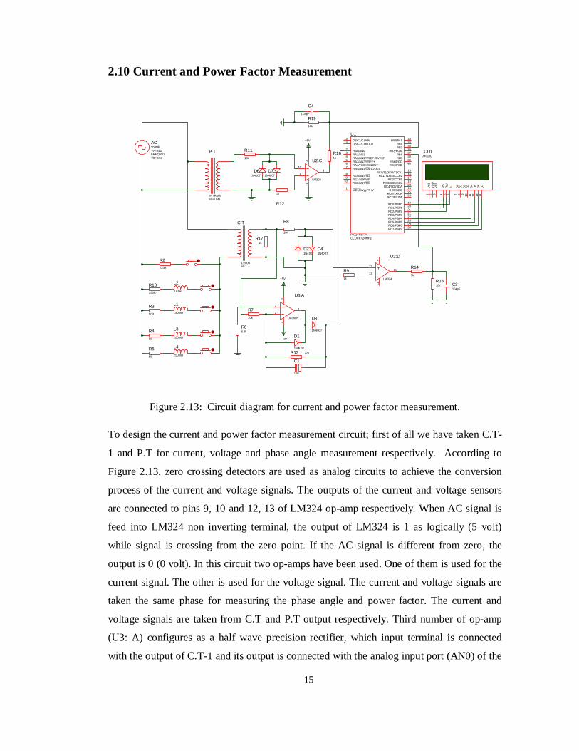
To design the current and power factor measurement circuit; first of all we have taken C.T-
1 and P.T for current, voltage and phase angle measurement respectively. According to
Figure 2.13, zero crossing detectors are used as analog circuits to achieve the conversion
process of the current and voltage signals. The outputs of the current and voltage sensors
are connected to pins 9, 10 and 12, 13 of LM324 op-amp respectively. When AC signal is
feed into LM324 non inverting terminal, the output of LM324 is 1 as logically (5 volt)
while signal is crossing from the zero point. If the AC signal is different from zero, the
output is 0 (0 volt). In this circuit two op-amps have been used. One of them is used for the
current signal. The other is used for the voltage signal. The current and voltage signals are
taken the same phase for measuring the phase angle and power factor. The current and
voltage signals are taken from C.T and P.T output respectively. Third number of op-amp
(U3: A) configures as a half wave precision rectifier, which input terminal is connected
with the output of C.T-1 and its output is connected with the analog input port (AN0) of the
16
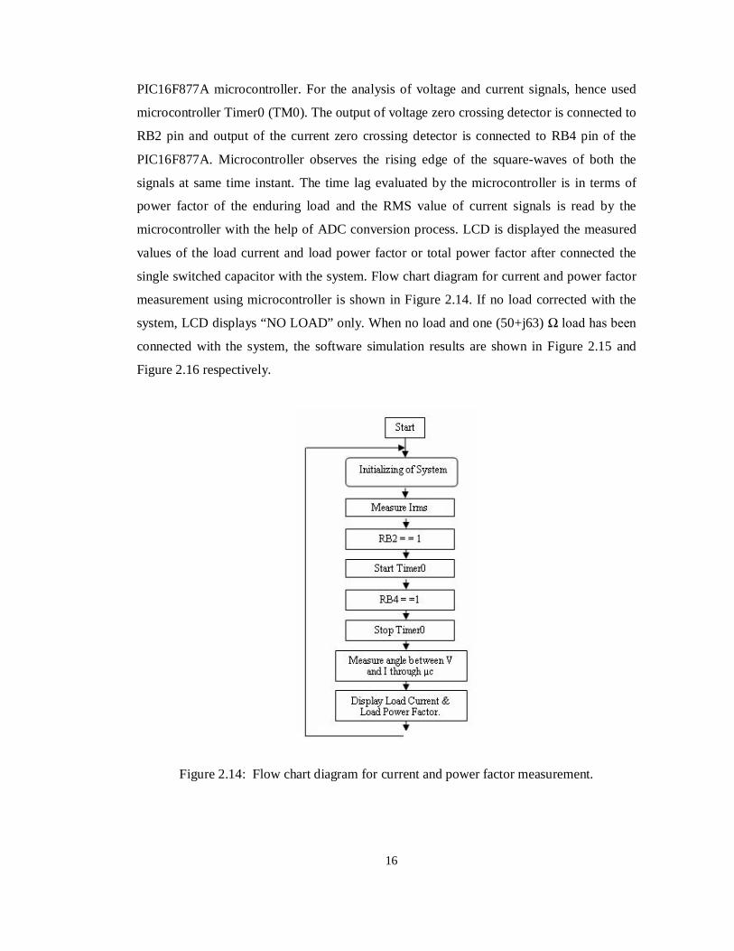
PIC16F877A microcontroller. For the analysis of voltage and current signals, hence used
microcontroller Timer0 (TM0). The output of voltage zero crossing detector is connected to
RB2 pin and output of the current zero crossing detector is connected to RB4 pin of the
PIC16F877A. Microcontroller observes the rising edge of the square-waves of both the
signals at same time instant. The time lag evaluated by the microcontroller is in terms of
power factor of the enduring load and the RMS value of current signals is read by the
microcontroller with the help of ADC conversion process. LCD is displayed the measured
values of the load current and load power factor or total power factor after connected the
single switched capacitor with the system. Flow chart diagram for current and power factor
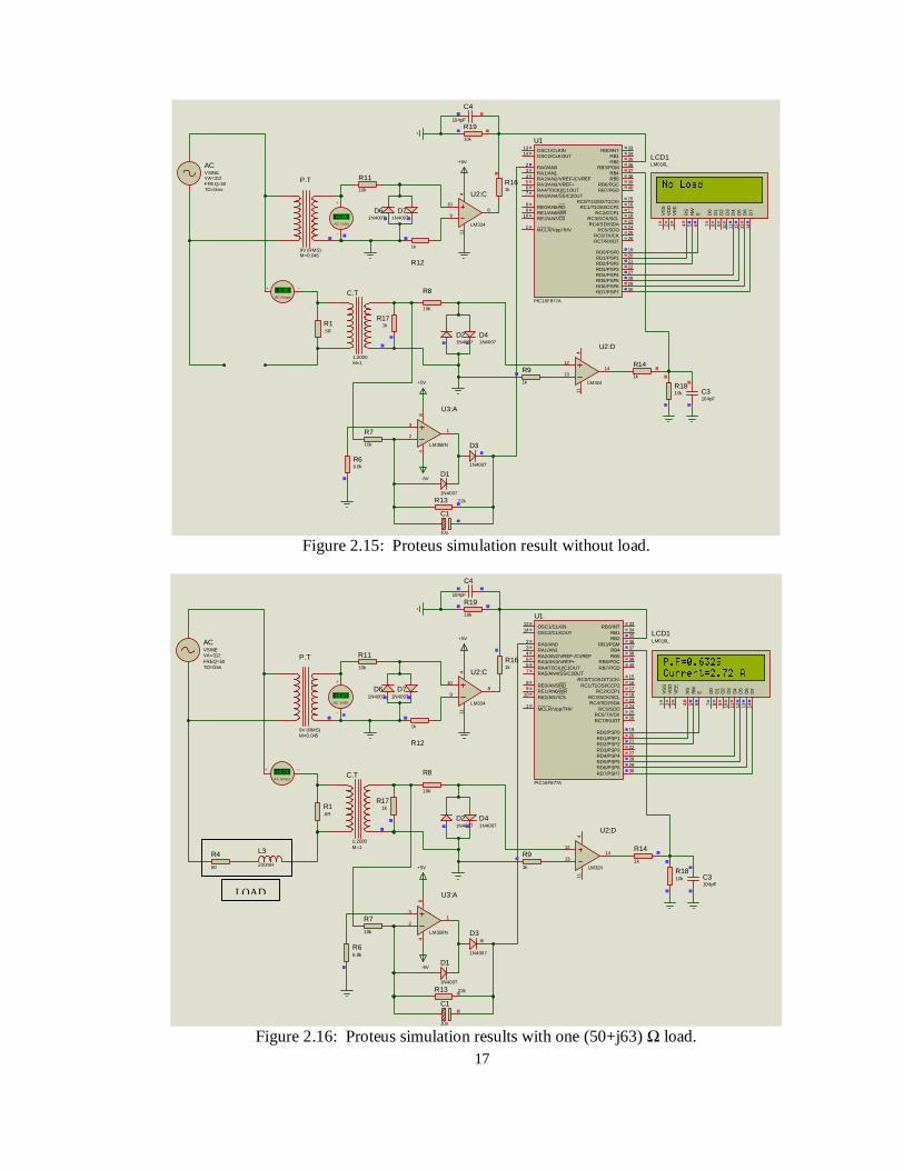
measurement using microcontroller is shown in Figure 2.14. If no load corrected with the
system, LCD displays “NO LOAD” only. When no load and one (50+j63) Ω load has been
connected with the system, the software simulation results are shown in Figure 2.15 and
Figure 2.16 respectively.
Figure 2.14: Flow chart diagram for current and power factor measurement.
17
ACVSINEVA=312FREQ=50TD=0ms
C.T
1:2000M=1
R1.5R
R8
10k
R1110k
R12
1k
AC Amps
0.00
P.T
9V (RMS)M=0.045
D3
1N4007
+5V
R66.8k
R7
10k
R13 22k
C1
10u
D1
1N4007
D21N4007
D41N4007
R141k
D61N4007
D71N4007
R161k
R171k
R1810k
R19
10k
10
98
411
U2:C
LM324AC Volts
+9.88
+5V
12
1314
411
U2:D
LM324
R91k
3
21
84
U3:A
LM358N
-5V
C3104pF
C4
104pF
RA0/AN02
RA1/AN13
RA2/AN2/VREF-/CVREF4
RA4/T0CKI/C1OUT6
RA5/AN4/SS/C2OUT7
RE0/AN5/RD8
RE1/AN6/WR9
RE2/AN7/CS10
OSC1/CLKIN13
OSC2/CLKOUT14
RC1/T1OSI/CCP2 16
RC2/CCP1 17
RC3/SCK/SCL 18
RD0/PSP0 19
RD1/PSP1 20
RB7/PGD 40RB6/PGC 39
RB5 38RB4 37
RB3/PGM 36RB2 35RB1 34
RB0/INT 33
RD7/PSP7 30RD6/PSP6 29RD5/PSP5 28RD4/PSP4 27RD3/PSP3 22RD2/PSP2 21
RC7/RX/DT 26RC6/TX/CK 25RC5/SDO 24RC4/SDI/SDA 23
RA3/AN3/VREF+5
RC0/T1OSO/T1CKI 15
MCLR/Vpp/THV1
U1
PIC16F877A
D7
14D
613
D5
12D
411
D3
10D
29
D1
8D
07
E6
RW5
RS
4
VS
S1
VD
D2
VE
E3
LCD1LM016L
Figure 2.15: Proteus simulation result without load.
ACVSINEVA=312FREQ=50TD=0ms
C.T
1:2000M=1
R1.5R
R8
10k
R1110k
R12
1k
AC Amps
+2.73
R4
50
L3
200mH
P.T
9V (RMS)M=0.045
D3
1N4007
+5V
R66.8k
R7
10k
R13 22k
C1
10u
D1
1N4007
D21N4007
D41N4007
R141k
D61N4007
D71N4007
R161k
R171k
R1810k
R1910k
10
98
411
U2:C
LM324AC Volts
+9.90
+5V
12
1314
411
U2:D
LM324
R9
1k
3
21
84
U3:A
LM358N
-5V
C3104pF
C4
104pF
RA0/AN02
RA1/AN13
RA2/AN2/VREF-/CVREF4
RA4/T0CKI/C1OUT6
RA5/AN4/SS/C2OUT7
RE0/AN5/RD8
RE1/AN6/WR9
RE2/AN7/CS10
OSC1/CLKIN13
OSC2/CLKOUT14
RC1/T1OSI/CCP2 16
RC2/CCP1 17
RC3/SCK/SCL 18
RD0/PSP0 19
RD1/PSP1 20
RB7/PGD 40RB6/PGC 39RB5 38RB4 37RB3/PGM 36RB2 35RB1 34RB0/INT 33
RD7/PSP7 30RD6/PSP6 29RD5/PSP5 28RD4/PSP4 27RD3/PSP3 22RD2/PSP2 21
RC7/RX/DT 26RC6/TX/CK 25RC5/SDO 24RC4/SDI/SDA 23
RA3/AN3/VREF+5
RC0/T1OSO/T1CKI 15
MCLR/Vpp/THV1
U1
PIC16F877A
D714
D613
D512
D411
D310
D29
D18
D07
E6
RW5
RS4
VSS
1
VDD
2
VEE
3
LCD1LM016L
Figure 2.16: Proteus simulation results with one (50+j63) Ω load.
LOAD
18
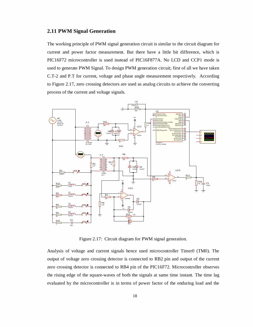
2.11 PWM Signal Generation
The working principle of PWM signal generation circuit is similar to the circuit diagram for
current and power factor measurement. But there have a little bit difference, which is
PIC16F72 microcontroller is used instead of PIC16F877A. No LCD and CCP1 mode is
used to generate PWM Signal. To design PWM generation circuit; first of all we have taken
C.T-2 and P.T for current, voltage and phase angle measurement respectively. According
to Figure 2.17, zero crossing detectors are used as analog circuits to achieve the converting
process of the current and voltage signals.
ACVSINEVA=312FREQ=50TD=0ms
L2
3.65H
R10353R
C.T
1:2000M=1
R1.5R
R8
10k
R1110k
R12
1k
+88.8AC Amps
R22300R
R350R
R450
L1
200mH
L3
200mH
R550
L4
250mH
P.T
9V (RMS)M=0.045
D3
1N4007
+5V
R66.8k
R7
10k
R13 22k
C1
10u
D1
1N4007
C2
35uf
R15
1
D21N4007
D41N4007
R141k
D61N4007
D71N4007
R161k
R171k
R1810k
R19
10k
10
98
411
U2:C
LM324+88.8
AC Volts
+5V
12
1314
411
U2:D
LM324
R91k
3
21
84
U3:A
LM358N
-5V
C3104pF
C4
104pF
RA0/AN02
RA1/AN13
RA2/AN2/VREF-/CVREF4
RA4/T0CKI/C1OUT6
RA5/AN4/SS/C2OUT7
OSC1/CLKIN9
OSC2/CLKOUT10
RC1/T1OSI/CCP2 12
RC2/CCP1 13
RC3/SCK/SCL 14
RB7/PGD 28RB6/PGC 27RB5 26RB4 25RB3/PGM 24RB2 23RB1 22RB0/INT 21
RC7/RX/DT 18RC6/TX/CK 17RC5/SDO 16RC4/SDI/SDA 15
RA3/AN3/VREF+5
RC0/T1OSO/T1CKI 11
MCLR/Vpp/THV1
U1
PIC16F72CLOCK=10MHz
A
B
C
D
Figure 2.17: Circuit diagram for PWM signal generation.
Analysis of voltage and current signals hence used microcontroller Timer0 (TM0). The
output of voltage zero crossing detector is connected to RB2 pin and output of the current
zero crossing detector is connected to RB4 pin of the PIC16F72. Microcontroller observes
the rising edge of the square-waves of both the signals at same time instant. The time lag
evaluated by the microcontroller is in terms of power factor of the enduring load and the
19
RMS value of current signals is read by the microcontroller using ADC process.
Microcontroller automatically selects the pulse width of the modulated signal according to
the program algorithm. Here RC2 (ccp1) pin is used as an output of the microcontroller
which is connected to the power MOSFET or IGBT gate via opto-isolated gate driver
circuit. When the duty cycle of the gate signal of power MOSFET or IGBT decrease or
increase as a result the voltage across the capacitor to control the compensating capacitive
current accordingly to attain unity power factor. Microcontroller dose not execute any
action if both the voltage and current square-waves are in phase i.e. measured power factor
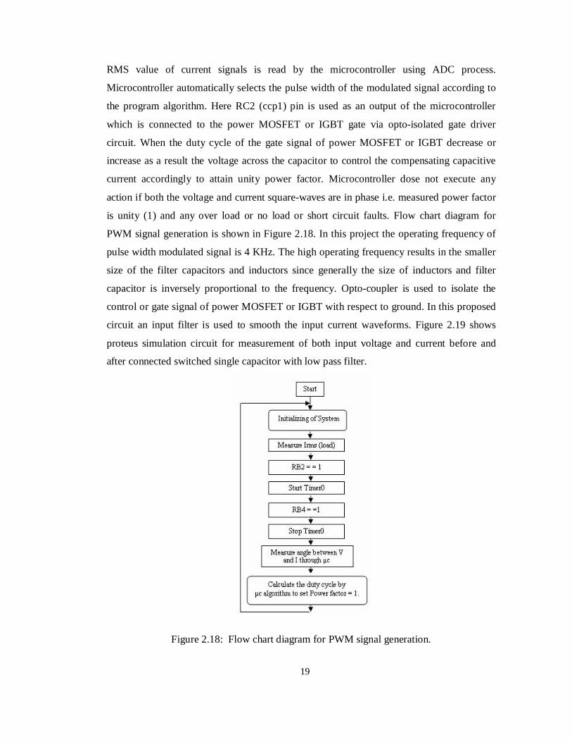
is unity (1) and any over load or no load or short circuit faults. Flow chart diagram for
PWM signal generation is shown in Figure 2.18. In this project the operating frequency of
pulse width modulated signal is 4 KHz. The high operating frequency results in the smaller
size of the filter capacitors and inductors since generally the size of inductors and filter
capacitor is inversely proportional to the frequency. Opto-coupler is used to isolate the
control or gate signal of power MOSFET or IGBT with respect to ground. In this proposed
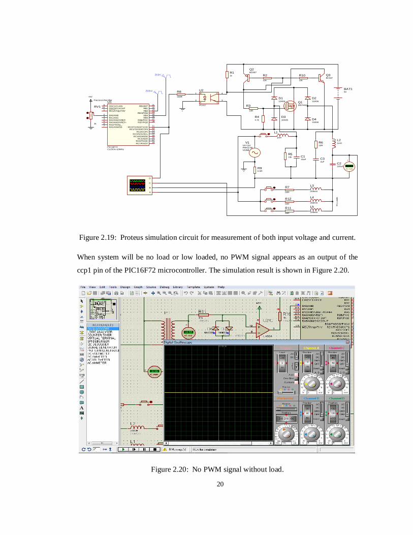
circuit an input filter is used to smooth the input current waveforms. Figure 2.19 shows
proteus simulation circuit for measurement of both input voltage and current before and
after connected switched single capacitor with low pass filter.
Figure 2.18: Flow chart diagram for PWM signal generation.
20
ZCD-V
ZCD-I
91%
RV1
1k
+5V
Precision Rectifier
R8330R D1
10A06D210A06
D310A06 D4
10A06
Q1IRFP460
BAT19V
Q2BC557R1
1k R210k
R310R
R44.7k
L1
1mH
A
K
C
E
1
2
4
3
U2
PC817
L21mH
C110uF
V1
VSINE
VA=312FREQ=50
R510k
C2100uF
R610R
C32uF
R750R
R90.5R
R-L
Loa
ds
A
B
C
D
+88.8AC Volts
Q3BC547
R1010k
R11
50R
R1250R
L4
250mH
L5
150mH
L3
200mH
RA0/AN02
RA1/AN13
RA2/AN2/VREF-4
RA4/T0CKI6
RA5/AN4/SS7
OSC1/CLKIN9
OSC2/CLKOUT10
RC1/T1OSI/CCP2 12
RC2/CCP1 13
RC3/SCK/SCL 14
RB7/PGD 28RB6/PGC 27RB5 26
RB4 25RB3/PGM 24RB2 23
RB1 22RB0/INT 21
RC7/RX/DT 18RC6/TX/CK 17
RC5/SDO 16RC4/SDI/SDA 15
RA3/AN3/VREF+5
RC0/T1OSO/T1CKI 11
MCLR/Vpp/THV1
U1
PIC16F72CLOCK=10MHz
Figure 2.19: Proteus simulation circuit for measurement of both input voltage and current.
When system will be no load or low loaded, no PWM signal appears as an output of the
ccp1 pin of the PIC16F72 microcontroller. The simulation result is shown in Figure 2.20.
Figure 2.20: No PWM signal without load.
21
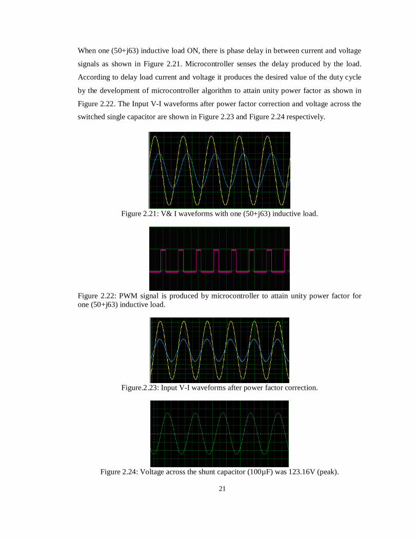
When one (50+j63) inductive load ON, there is phase delay in between current and voltage
signals as shown in Figure 2.21. Microcontroller senses the delay produced by the load.
According to delay load current and voltage it produces the desired value of the duty cycle
by the development of microcontroller algorithm to attain unity power factor as shown in
Figure 2.22. The Input V-I waveforms after power factor correction and voltage across the
switched single capacitor are shown in Figure 2.23 and Figure 2.24 respectively.
Figure 2.21: V& I waveforms with one (50+j63) inductive load.
Figure 2.22: PWM signal is produced by microcontroller to attain unity power factor for one (50+j63) inductive load.
Figure.2.23: Input V-I waveforms after power factor correction.
Figure 2.24: Voltage across the shunt capacitor (100µF) was 123.16V (peak).
22
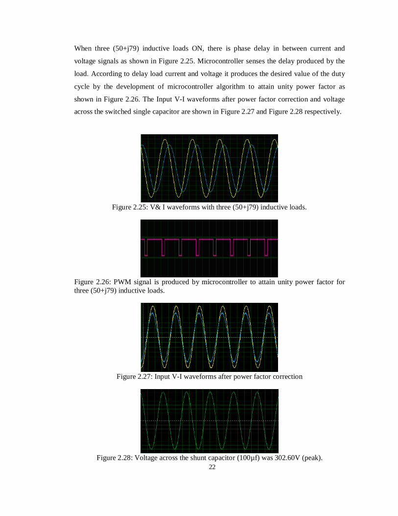
When three (50+j79) inductive loads ON, there is phase delay in between current and
voltage signals as shown in Figure 2.25. Microcontroller senses the delay produced by the
load. According to delay load current and voltage it produces the desired value of the duty
cycle by the development of microcontroller algorithm to attain unity power factor as
shown in Figure 2.26. The Input V-I waveforms after power factor correction and voltage
across the switched single capacitor are shown in Figure 2.27 and Figure 2.28 respectively.
Figure 2.25: V& I waveforms with three (50+j79) inductive loads.
Figure 2.26: PWM signal is produced by microcontroller to attain unity power factor for three (50+j79) inductive loads.
Figure 2.27: Input V-I waveforms after power factor correction
Figure 2.28: Voltage across the shunt capacitor (100µf) was 302.60V (peak).
23
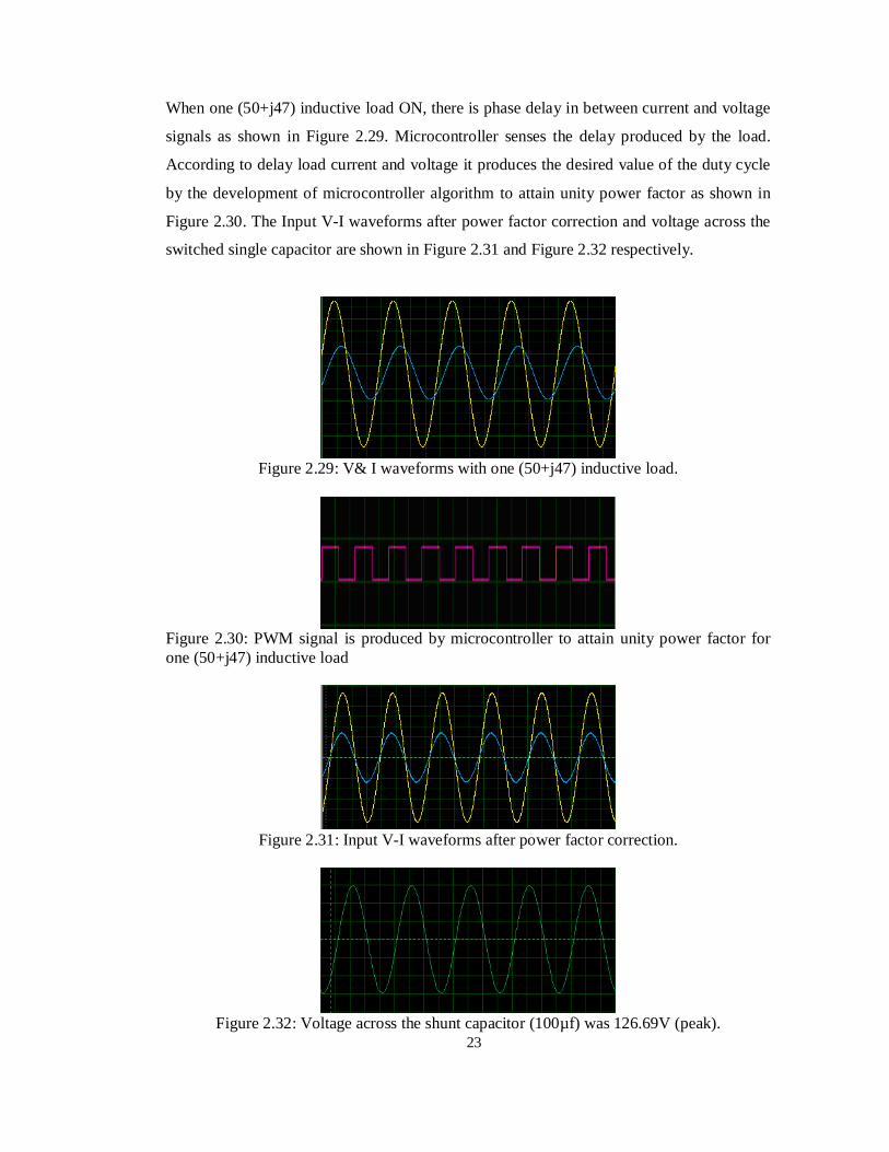
When one (50+j47) inductive load ON, there is phase delay in between current and voltage
signals as shown in Figure 2.29. Microcontroller senses the delay produced by the load.
According to delay load current and voltage it produces the desired value of the duty cycle
by the development of microcontroller algorithm to attain unity power factor as shown in
Figure 2.30. The Input V-I waveforms after power factor correction and voltage across the
switched single capacitor are shown in Figure 2.31 and Figure 2.32 respectively.
Figure 2.29: V& I waveforms with one (50+j47) inductive load.
Figure 2.30: PWM signal is produced by microcontroller to attain unity power factor for one (50+j47) inductive load
Figure 2.31: Input V-I waveforms after power factor correction.
Figure 2.32: Voltage across the shunt capacitor (100µf) was 126.69V (peak).

24
Chapter 3
Implementation of the Proposed Power Factor Correction Circuit
3.1 Introduction In this project PIC microcontroller based power factor correction by using switched single
capacitor is designed and simulated step by step starting from dual power supply unit using
simulation software. Finally the proposed project is implemented in the laboratory and
performance of the power factor correction circuit is observed by using oscilloscope and
LCD displayed values. The following components have been used to implement proposed
project and technical specifications with pin configuration of each component are given
below.
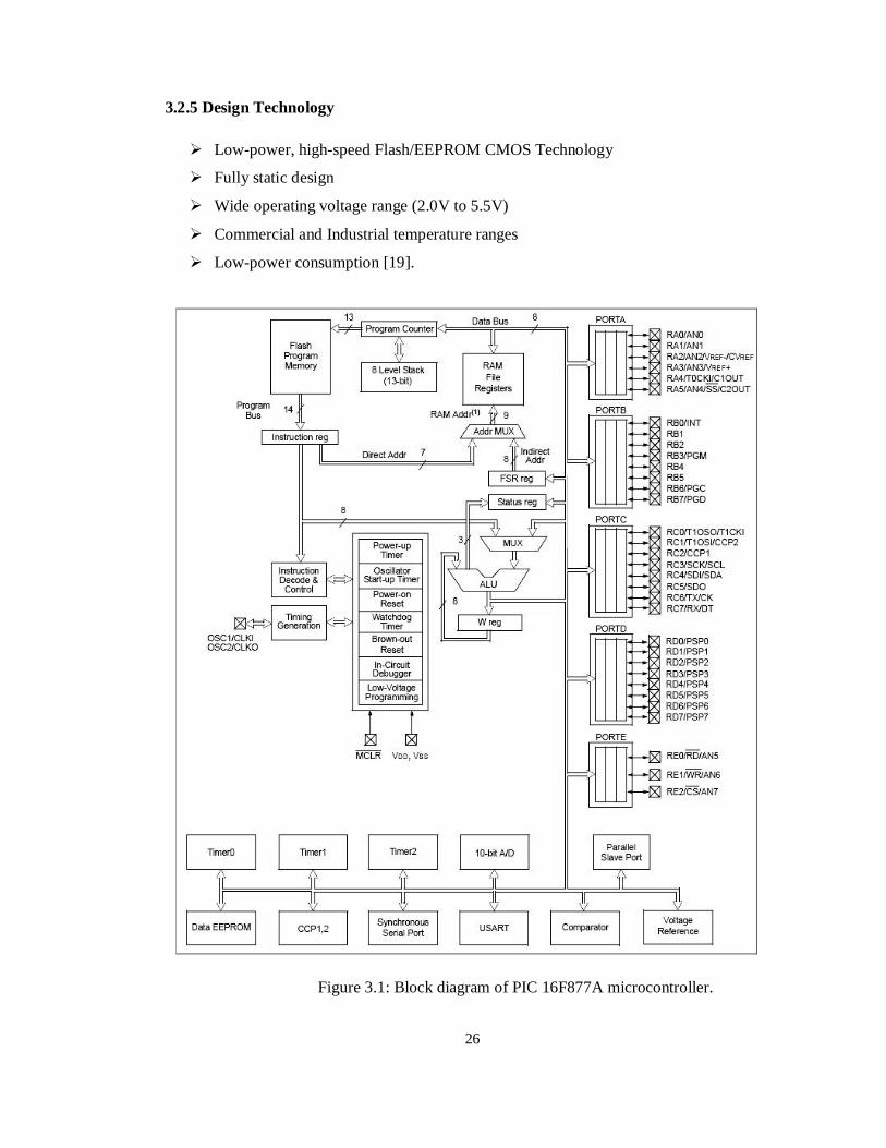
3.2 PIC16F877A 40-Pin Enhanced Flash Microcontroller A microcontroller is a computer control system on a single chip. It has many electronic
circuits built into it, which can decode written instructions and convert them to electrical
signals. The microcontroller will then step through these instructions and execute them one
by one. The list of these instructions given to the microcontroller is called a program. There
are different types of microcontroller, this project focus only on the PIC16F877A and
PIC16F72 Microcontrollers. Figure 3.1 and Figure 3.2 shows internal block diagram and
pin configuration of PIC16F877A microcontroller respectively.
3.2.1 High-Performance RISC CPU
Only 35 single-word instructions to learn
Operating speed: DC – 20 MHz clock input
Up to 8K x 14 words of Flash Program Memory
-Up to 256 x 8 bytes of EEPROM Data Memory
3.2.2 Peripheral Features
Timer0: 8-bit timer/counter with 8-bit pre scalar
Timer1: 16-bit timer/counter with pre scalar.

25
Timer2: 8-bit timer/counter with 8-bit period register, pre scalar and post scalar
Two Capture, Compare, PWM modules
- Capture is 16-bit, maximum resolution is 12.5 ns
- Compare is 16-bit, maximum resolution is 200 ns
- PWM maximum resolution is 10-bit
Synchronous Serial Port (SSP) with SPI (Master mode) and I2C™ (Master/Slave)
Universal Synchronous Asynchronous Receiver Transmitter (USART/SCI) with 9-
bit address detection
Parallel Slave Port (PSP) – 8 bits wide with external RD, WR and CS controls
(40/44 pin only)
Brown-out detection circuitry for Brown-out Reset (BOR)
3.2.3 Analog Features
10-bit, up to 8-channel Analog-to-Digital Converter (A/D)
Brown-out Reset (BOR)
Analog Comparator module with:
- Two analog comparators
- Programmable on-chip voltage reference (VREF) module
- Comparator outputs are externally accessible
3.2.4 Special Microcontroller Features
100,000 erase/write cycle Enhanced Flash Program memory typical
1,000,000 erase/write cycle Data EEPROMM memory typical
Data EEPROM Retention > 40 years
Self-reprogrammable under software control
In-Circuit Serial Programming™ (ICSP™) Via two pins
Single-supply 5V In-Circuit Serial Programming
Watchdog Timer (WDT) with its own on-chip RC Oscillator for reliable operation
Programmable code protection
Power saving Sleep mode
Selectable oscillator options
In-Circuit Debug (ICD) via two pin
26
3.2.5 Design Technology
Low-power, high-speed Flash/EEPROM CMOS Technology
Fully static design
Wide operating voltage range (2.0V to 5.5V)
Commercial and Industrial temperature ranges
Low-power consumption [19].
Figure 3.1: Block diagram of PIC 16F877A microcontroller.

27
3.2.6 Pin Diagram of PIC16F877A
Figure 3.2: Pin configuration of PIC 16F877A microcontroller.
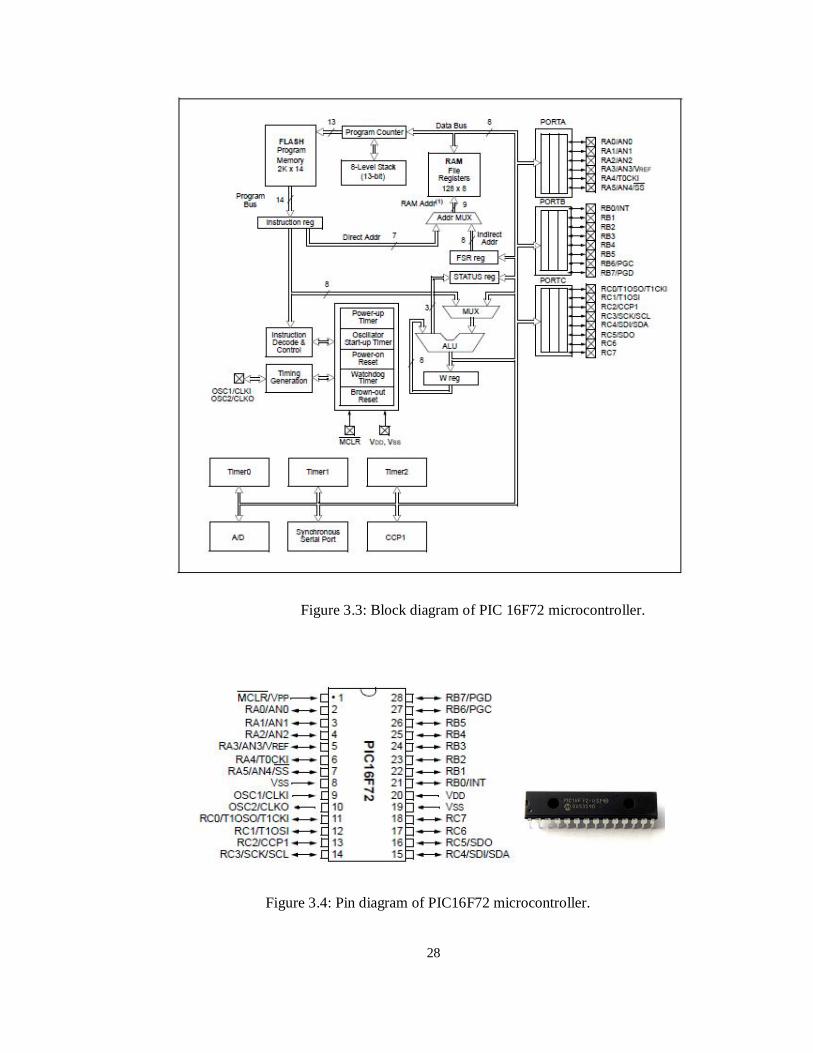
3.3 PIC16F72 28-Pin Enhanced Flash Microcontroller The PIC16F72 belongs to the Mid-Range family of the PIC micro devices. The program
memory contains 2K words, which translate to 2048 instructions, since each 14-bit program
memory word is the same width as each device instruction. The data memory (RAM)
contains 128 bytes. There are 22 I/O pins that are user configurable on a pin-to-pin basis.
Some pins are multiplexed with other device functions [20]. Figure 3.3 and Figure 3.4 is
shown internal block diagram and pin configuration of PIC16F72 microcontroller
respectively.
These functions include:
External interrupt
Change on PORTB interrupts
Timer0 clock input
Timer1 clock/oscillator
Capture/Compare/PWM
A/D converter
SPI/I2C
Low Voltage Programming
In circuit Debugger
28
Figure 3.3: Block diagram of PIC 16F72 microcontroller.
Figure 3.4: Pin diagram of PIC16F72 microcontroller.
29
3.3.1 Pin Description
MCLR/VPP:
Master Clear (Reset) input or programming voltage input. This pin is an active low
RESET to the device.
RA0 - RA5:
These are the bi-directional Input / output PORTA pins.
RA1, RA2, are the analog inputs 1, analog input2.
RA3 can also be analog input3 or analog reference voltage.
RA4 can also be the clock input to the Timer0 module. Output is open drain type.
RA5 can also be analog input4 or the slave select for the synchronous serial port.
VSS:
Ground reference for logic and I/O pins.
OSC1/CLK1:
Oscillator crystal input / External clock source input.
OSC2/CLKO:
Oscillator crystal output Connects to crystal or resonator in Crystal Oscillator mode.
In RC mode, the OSC2 pin outputs CLKO, which has 1/4 the frequency of OSC1, and
denotes the instruction cycle rate.
RC0 – RC7:
These are the bidirectional Input / Output PORTC pins.
RC0/T1OSO/ T1CK RC0 can also be the Timer1 oscillator output or Timer1
Clock input:
RC1/T1OSI is the Timer1 oscillator input.
RC2/CCP is the Capture1 input/Compare1 output/ PWM1 output.
RC3/SCK/SCL RC3 can also be the synchronous serial clock input/output for
Both SPI and I2C modes

30
RC4/SDI/SDA is the SPI Data In (SPI mode) or Data I/O (I2C mode).
RC5/SDO is e the SPI Data Out (SPI mode).
RC6
RC7.
VDD:
Positive supply for logic and I/O pins.
RB0 – RB7:
These are the bi-directional I/O PORTB pins. PORTB can be software
Programmed for internal weak pull-up on all inputs
RB0/IN is the external interrupt pin.
RB1, RB2, RB3 are the bi-directional pins.
RB4 is the Interrupt-on-change pin.
RB5 is the Interrupt-on-change pin.
RB6/PGC is the Interrupt-on-change pin. Serial programming clock
RB7/PGD is the Interrupt-on-change pin. Serial programming data
Oscillator configurations:
The PIC16F72 can be operated in four different Oscillator modes. The user can program
two configuration bits (FOSC1 and FOSC0) to select one of these four Modes:
• LP Low Power Crystal
• XT Crystal/Resonator
• HS High Speed Crystal/Resonator
• RC Resistor/Capacitor
3.4 Regulated IC L7805CV
L7805CV is an easy to use voltage regulator IC which output 5 volts and 1 A max. 7805 is
positive regulator IC.L7805CV is a voltage regulator integrated circuit. It is a member of
78xx series of fixed linear voltage regulator ICs. The voltage source in a circuit may have
fluctuation and would not give the fixed voltage output. The voltage regulated IC maintain
the output voltage at a constant value. The xx in 78xx indicates the fixed output voltage it is
31
designed to provide.7805 provides +5V regulated power supply. Capacitor of suitable value
can be connected at input pins depending upon the respective voltage level. A typical
L7805 linear voltage regulator is shown in Figure 3.5.
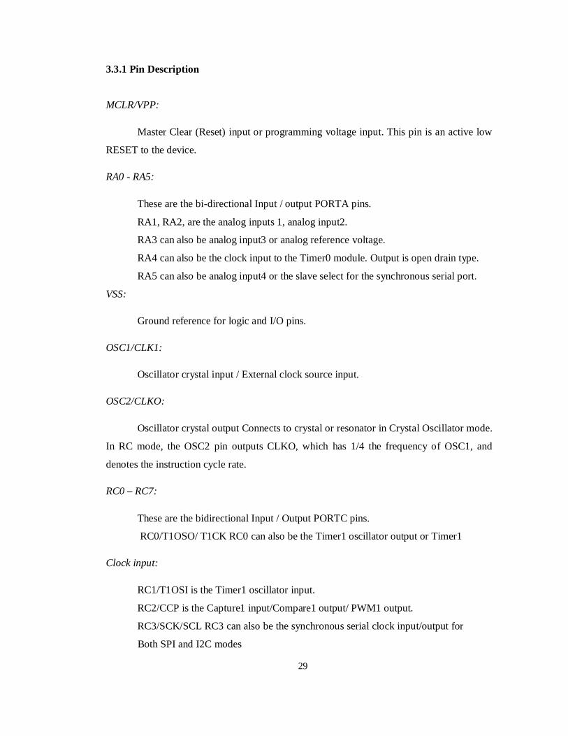
Figure 3.5: L7805CV +5V linear voltage regulator.
3.4.1 Features
Output current up to 1.5 A
Output voltage of 5; 6; 8; 8.5; 9; 12; 15; 18; 24V
Thermal overload & Short circuit protection.
2% output voltage tolerance (A version).
Guaranteed in extended temperature range [21].
3.5 Capacitor In this proposed project, capacitor supposed to be chosen with minimum loss because
power regulators are usually used in high current-performance power supplies. Loss occurs
because of its internal series resistance and inductance. Commonly capacitors for switched
regulators are chosen based on the equivalent series resistance. In this project, 0.1μF
(104pF) ceramic and 10 μF /50 V-dc electrolyte capacitors were used at the output of the
LM7805 and LM7905 IC to smoothing the output voltage from DC ripples and to withstand
during switching and transient effects. A typical ceramic and an electrolyte capacitor are
shown in Figure 3.6.
Figure 3.6: A ceramic capacitor and an electrolyte capacitor respectively.

32
3.6 NPN Silicon Transistors (BC547N) In this project we have used BC547N NPN Silicon Transistor, which is a highly
performance switching device. Its Collector-Base Voltage is 50 V, maximum, collector to
emitter voltage is 45 v maximum, Emitter to base voltage is 5 V, collector current is 100
mA, when input signal is zero, maximum collector power dissipation is 500 milli watt. Its
switching frequency is 300 MHz; This Transistor is used in my project as a high power
IGBT / N-MOS gate driver circuit component [22]. A typical BC547N NPN Silicon
Transistor is shown in the following Figure 3.7.
Figure 3.7: Typical BC547N silicon transistor.
3.7 PNP Silicon Transistor (BC557) In this project we have used BC557 PNP Silicon Transistor, which is a highly performance
switching device. Its Collector-Base Voltage is -50 V, maximum, collector to emitter
voltage is -45 v maximum, Emitter to base voltage is -5 V, collector current is -100 mA,
when input signal is zero, maximum collector power dissipation is 500 milli watt. Its
switching frequency is 150 MHz; This Transistor is used in my project as a high power
IGBT / N-MOS gate driver circuit component [22]. A typical BC557 PNP Silicon
Transistor is shown in the following Figure 3.8.
Figure 3.8: Typical BC557 silicon transistor.
33
3.8 Power MOSFET (IRFP460) The power MOSFET current rating is related with the heat dissipated in the device. This
rating will be taken in consideration for designing appropriate circuit to protect power
MOSFET against high voltage and current, thus cause heat generation. While considering
protection of power MOSFET against over voltage, a distinction has to be made between
slowly varying over voltage and short time surge. It is about 500Vdc the maximum rating
of drain to source break down voltage. Maximum gate to source voltage ±20V.Its
maximum power dissipation is 280W at 25ºC and continuous drain current is 20A. Its
switching frequency range is 1MHz (Max.) [23]. A typical power N channel MOSFET
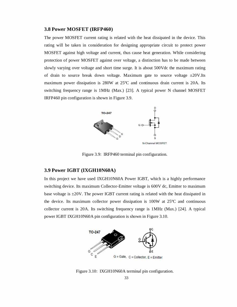
IRFP460 pin configuration is shown in Figure 3.9.
Figure 3.9: IRFP460 terminal pin configuration.
3.9 Power IGBT (IXGH10N60A) In this project we have used IXGH10N60A Power IGBT, which is a highly performance
switching device. Its maximum Collector-Emitter voltage is 600V dc, Emitter to maximum
base voltage is ±20V. The power IGBT current rating is related with the heat dissipated in
the device. Its maximum collector power dissipation is 100W at 25ºC and continuous
collector current is 20A. Its switching frequency range is 1MHz (Max.) [24]. A typical
power IGBT IXGH10N60A pin configuration is shown in Figure 3.10.
Figure 3.10: IXGH10N60A terminal pin configuration.
34
3.10 Opto-Coupler (4N25) An opto-isolator (also known as optical coupler, opto-coupler and opto-isolator) is a
semiconductor device that uses a short optical transmission path to transfer an electrical
signal between circuits or elements of a circuit, while keeping them electrically isolated
from each other. These components are used in a wide variety of communications, control
and monitoring systems that use light to prevent electrical high voltage from affecting a
lower power system receiving a signal. In its simplest form, an opto-isolator consists of a
light-emitting diode (LED), IRED (infrared-emitting diode) or laser diode for signal
transmission and a photo sensor (or phototransistor) for signal reception. Internal structure
of an opto-coupler is shown in Figure 3.11.
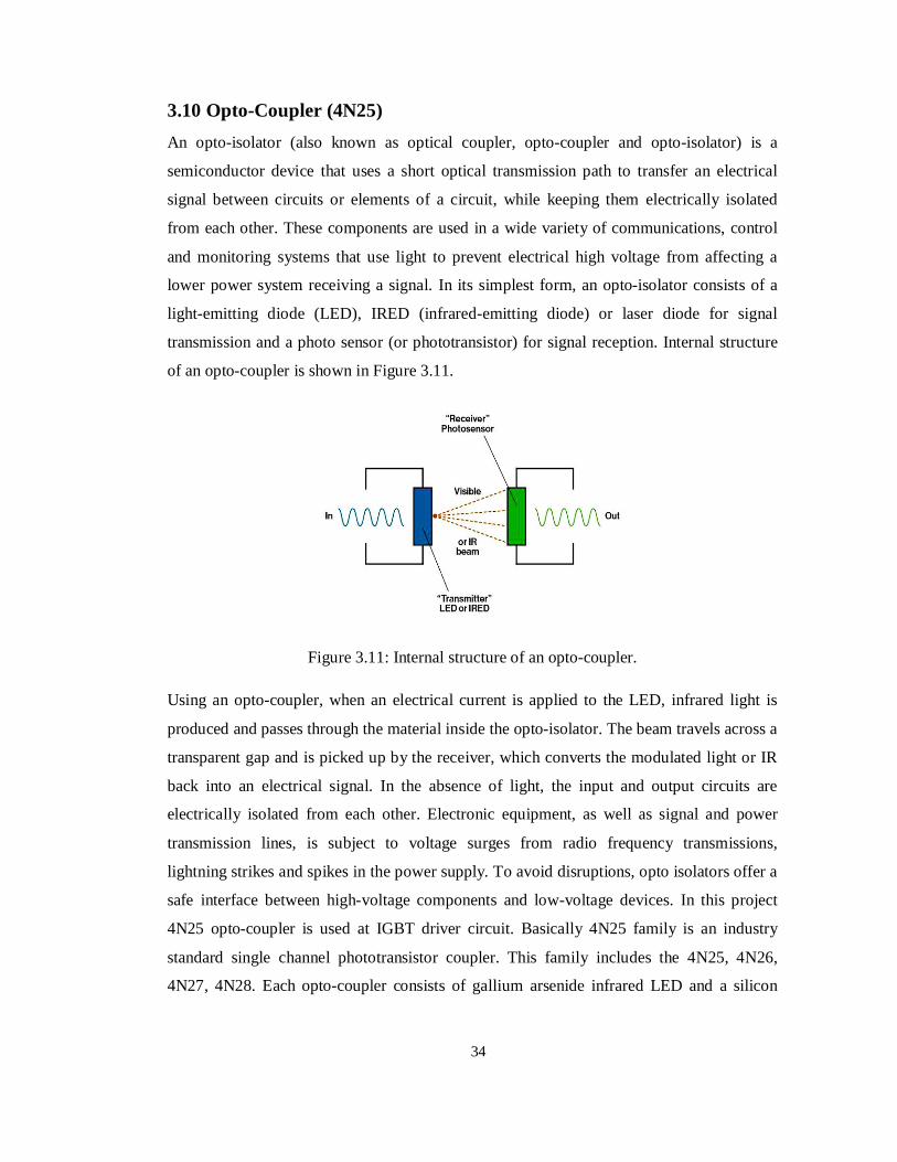
Figure 3.11: Internal structure of an opto-coupler.
Using an opto-coupler, when an electrical current is applied to the LED, infrared light is
produced and passes through the material inside the opto-isolator. The beam travels across a
transparent gap and is picked up by the receiver, which converts the modulated light or IR
back into an electrical signal. In the absence of light, the input and output circuits are
electrically isolated from each other. Electronic equipment, as well as signal and power
transmission lines, is subject to voltage surges from radio frequency transmissions,
lightning strikes and spikes in the power supply. To avoid disruptions, opto isolators offer a
safe interface between high-voltage components and low-voltage devices. In this project
4N25 opto-coupler is used at IGBT driver circuit. Basically 4N25 family is an industry
standard single channel phototransistor coupler. This family includes the 4N25, 4N26,
4N27, 4N28. Each opto-coupler consists of gallium arsenide infrared LED and a silicon
35
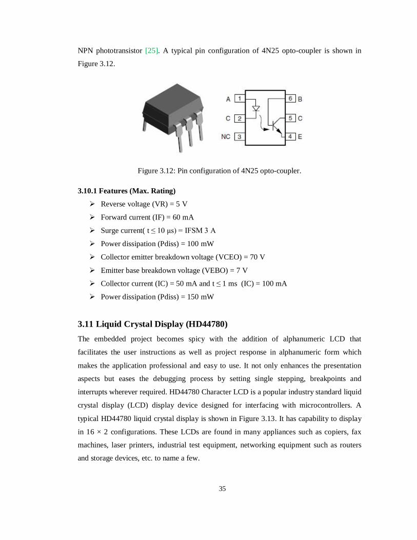
NPN phototransistor [25]. A typical pin configuration of 4N25 opto-coupler is shown in
Figure 3.12.
Figure 3.12: Pin configuration of 4N25 opto-coupler.
3.10.1 Features (Max. Rating)
Reverse voltage (VR) = 5 V
Forward current (IF) = 60 mA
Surge current( t ≤ 10 μs) = IFSM 3 A
Power dissipation (Pdiss) = 100 mW
Collector emitter breakdown voltage (VCEO) = 70 V
Emitter base breakdown voltage (VEBO) = 7 V
Collector current (IC) = 50 mA and t ≤ 1 ms (IC) = 100 mA
Power dissipation (Pdiss) = 150 mW
3.11 Liquid Crystal Display (HD44780) The embedded project becomes spicy with the addition of alphanumeric LCD that
facilitates the user instructions as well as project response in alphanumeric form which
makes the application professional and easy to use. It not only enhances the presentation
aspects but eases the debugging process by setting single stepping, breakpoints and
interrupts wherever required. HD44780 Character LCD is a popular industry standard liquid
crystal display (LCD) display device designed for interfacing with microcontrollers. A
typical HD44780 liquid crystal display is shown in Figure 3.13. It has capability to display
in 16 × 2 configurations. These LCDs are found in many appliances such as copiers, fax
machines, laser printers, industrial test equipment, networking equipment such as routers
and storage devices, etc. to name a few.
36
Manufacture’s data sheet and even many web pages cover the commands for the LCD. By
adding a shift register a two wire interface for the LCD is also been developed.
Figure 3.13: HD44780 liquid crystal display (LCD).
3.11.1 Features
Wide viewing angle and high contrast
Industry standard HD44780 equivalent LCD controller built-in
+5V DC LED backlight
don’t need separate power supply for backlight
Supported 4 or 8 bit parallel interface
Display 2-line X 16-character
Operate with 5V DC
Free 16 positions male header
3.11.2 Specifications
Module Size (W x H x T): 80mm X 36mm X 14mm
Black Metal Bezel (W x H): 72.2mm X 24.1mm
Viewing Area (W x H): 64.5mm X 14.5mm
3.11.3 Pin Description
Pin 7 to pin 14-All 8 pins are responsible for the transfer of data.
Pin 4-This is RS i.e., register select pin.
Pin 5-This is R/W i.e., Read/Write pin.
Pin 6-This is E i.e., enable pin.
Pin 2-This is VDD i.e., power supply pin.
Pin 1-This is VSS i.e., ground pin.
Pin 3-This is short pin
37
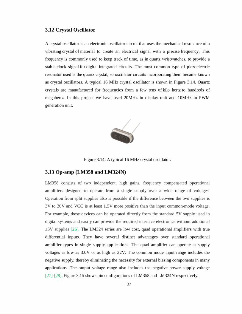
3.12 Crystal Oscillator A crystal oscillator is an electronic oscillator circuit that uses the mechanical resonance of a
vibrating crystal of material to create an electrical signal with a precise frequency. This
frequency is commonly used to keep track of time, as in quartz wristwatches, to provide a
stable clock signal for digital integrated circuits. The most common type of piezoelectric
resonator used is the quartz crystal, so oscillator circuits incorporating them became known
as crystal oscillators. A typical 16 MHz crystal oscillator is shown in Figure 3.14. Quartz
crystals are manufactured for frequencies from a few tens of kilo hertz to hundreds of
megahertz. In this project we have used 20MHz in display unit and 10MHz in PWM
generation unit.
Figure 3.14: A typical 16 MHz crystal oscillator.
3.13 Op-amp (LM358 and LM324N)
LM358 consists of two independent, high gains, frequency compensated operational
amplifiers designed to operate from a single supply over a wide range of voltages.
Operation from split supplies also is possible if the difference between the two supplies is
3V to 30V and VCC is at least 1.5V more positive than the input common-mode voltage.
For example, these devices can be operated directly from the standard 5V supply used in
digital systems and easily can provide the required interface electronics without additional
±5V supplies [26]. The LM324 series are low cost, quad operational amplifiers with true
differential inputs. They have several distinct advantages over standard operational
amplifier types in single supply applications. The quad amplifier can operate at supply
voltages as low as 3.0V or as high as 32V. The common mode input range includes the
negative supply, thereby eliminating the necessity for external biasing components in many
applications. The output voltage range also includes the negative power supply voltage
[27]-[28]. Figure 3.15 shows pin configurations of LM358 and LM324N respectively.
38
Figure 3.15: Pin configurations of LM358 and LM324N respectively.
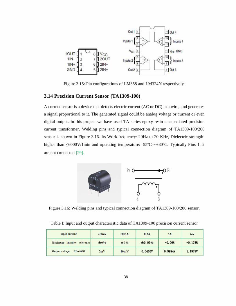
3.14 Precision Current Sensor (TA1309-100)
A current sensor is a device that detects electric current (AC or DC) in a wire, and generates
a signal proportional to it. The generated signal could be analog voltage or current or even
digital output. In this project we have used TA series epoxy resin encapsulated precision
current transformer. Welding pins and typical connection diagram of TA1309-100/200
sensor is shown in Figure 3.16. Its Work frequency: 20Hz to 20 KHz, Dielectric strength:
higher than ≤6000V/1min and operating temperature: -55ºC~+80ºC. Typically Pins 1, 2
are not connected [29].
Figure 3.16: Welding pins and typical connection diagram of TA1309-100/200 sensor.
Table I: Input and output characteristic data of TA1309-100 precision current sensor
39
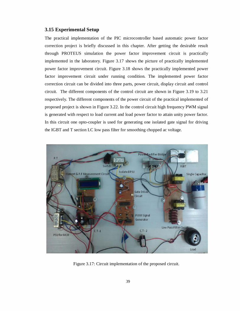
3.15 Experimental Setup The practical implementation of the PIC microcontroller based automatic power factor
correction project is briefly discussed in this chapter. After getting the desirable result
through PROTEUS simulation the power factor improvement circuit is practically
implemented in the laboratory. Figure 3.17 shows the picture of practically implemented
power factor improvement circuit. Figure 3.18 shows the practically implemented power
factor improvement circuit under running condition. The implemented power factor
correction circuit can be divided into three parts, power circuit, display circuit and control
circuit. The different components of the control circuit are shown in Figure 3.19 to 3.21
respectively. The different components of the power circuit of the practical implemented of
proposed project is shown in Figure 3.22. In the control circuit high frequency PWM signal
is generated with respect to load current and load power factor to attain unity power factor.
In this circuit one opto-coupler is used for generating one isolated gate signal for driving
the IGBT and T section LC low pass filter for smoothing chopped ac voltage.
Figure 3.17: Circuit implementation of the proposed circuit.
40
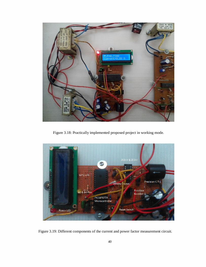
Figure 3.18: Practically implemented proposed project in working mode.
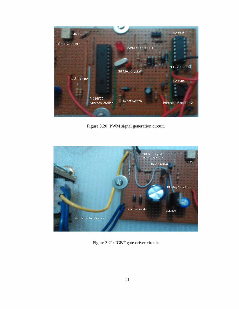
Figure 3.19: Different components of the current and power factor measurement circuit.
41
Figure 3.20: PWM signal generation circuit.
Figure 3.21: IGBT gate driver circuit.
42
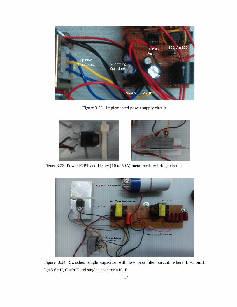
Figure 3.22: Implemented power supply circuit.
Figure 3.23: Power IGBT and Heavy (10 to 50A) metal rectifier bridge circuit.
Figure 3.24: Switched single capacitor with low pass filter circuit; where L1=5.6mH,
L2=5.6mH, C1=2uF and single capacitor =10uF.
43
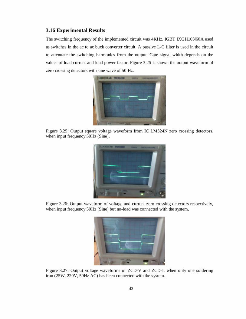
3.16 Experimental Results The switching frequency of the implemented circuit was 4KHz. IGBT IXGH10N60A used
as switches in the ac to ac buck converter circuit. A passive L-C filter is used in the circuit
to attenuate the switching harmonics from the output. Gate signal width depends on the
values of load current and load power factor. Figure 3.25 is shown the output waveform of
zero crossing detectors with sine wave of 50 Hz.
Figure 3.25: Output square voltage waveform from IC LM324N zero crossing detectors, when input frequency 50Hz (Sine).
Figure 3.26: Output waveform of voltage and current zero crossing detectors respectively, when input frequency 50Hz (Sine) but no-load was connected with the system.
Figure 3.27: Output voltage waveforms of ZCD-V and ZCD-I, when only one soldering iron (25W, 220V, 50Hz AC) has been connected with the system.
44
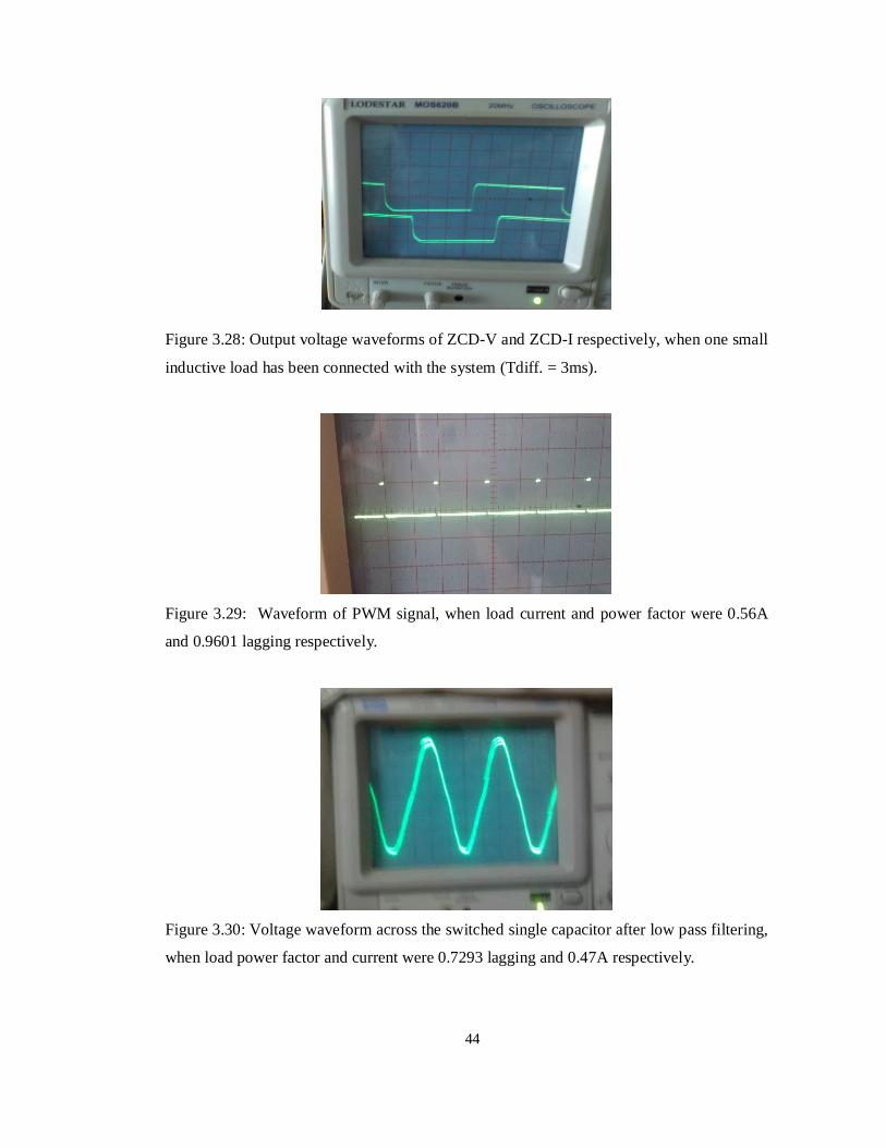
Figure 3.28: Output voltage waveforms of ZCD-V and ZCD-I respectively, when one small
inductive load has been connected with the system (Tdiff. = 3ms).
Figure 3.29: Waveform of PWM signal, when load current and power factor were 0.56A
and 0.9601 lagging respectively.
Figure 3.30: Voltage waveform across the switched single capacitor after low pass filtering,
when load power factor and current were 0.7293 lagging and 0.47A respectively.
45
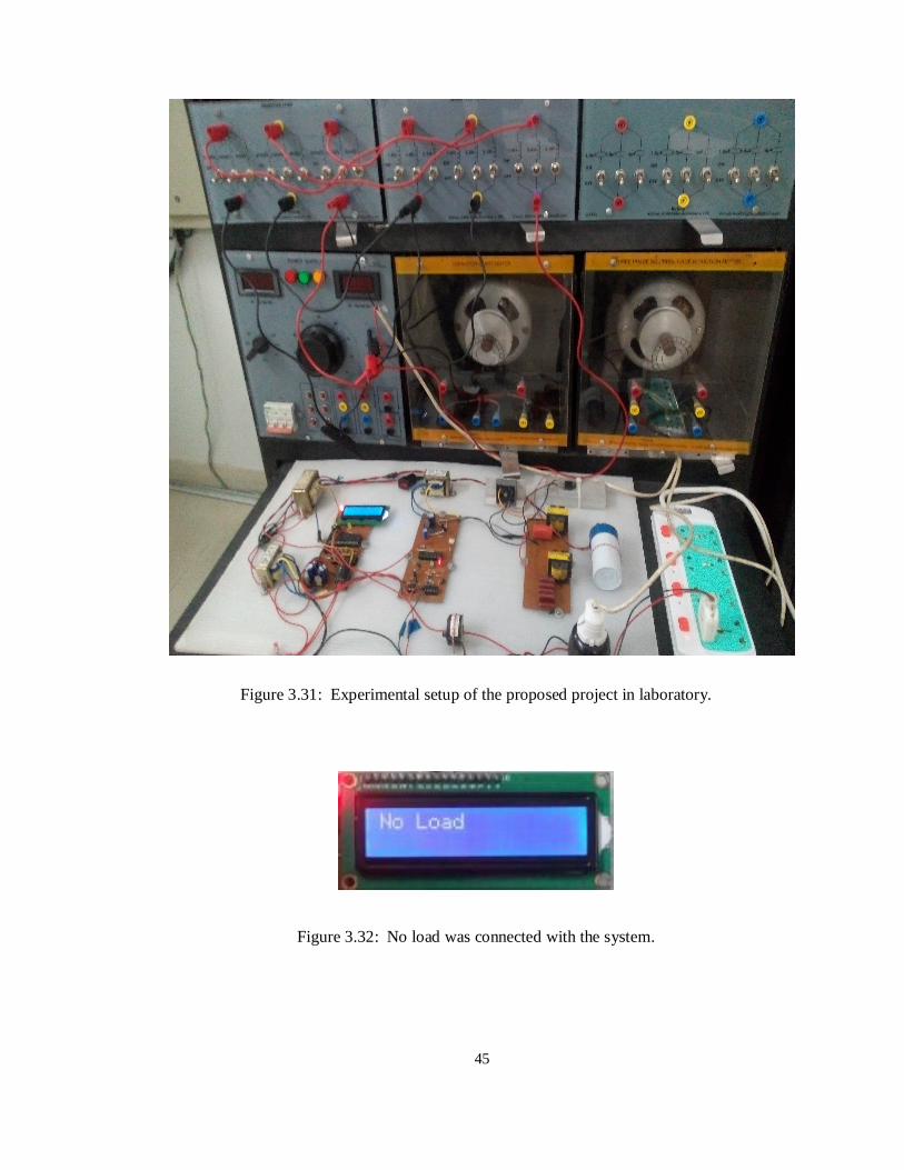
Figure 3.31: Experimental setup of the proposed project in laboratory.
Figure 3.32: No load was connected with the system.

46
Before Power Factor Correction After Power Factor Correction
Figure 3.33: Real-time results, (a) without switched single capacitor (displayed load current
and load power factor), (b) after connecting switched single capacitor across the load(s)
(displayed resultant current / circuit input current and overall power factor).
47
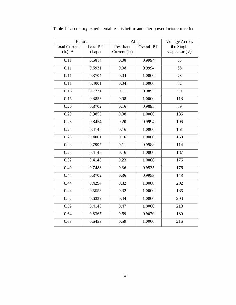
Table-I: Laboratory experimental results before and after power factor correction.
Before After Voltage Across the Single
Capacitor (V) Load Current
(IL), A Load P.F
(Lag.) Resultant
Current (IR) Overall P.F
0.11 0.6814 0.08 0.9994 65
0.11 0.6931 0.08 0.9994 58
0.11 0.3704 0.04 1.0000 78
0.11 0.4001 0.04 1.0000 82
0.16 0.7271 0.11 0.9895 90
0.16 0.3853 0.08 1.0000 118
0.20 0.8702 0.16 0.9895 79
0.20 0.3853 0.08 1.0000 136
0.23 0.8454 0.20 0.9994 106
0.23 0.4148 0.16 1.0000 151
0.23 0.4001 0.16 1.0000 169
0.23 0.7997 0.11 0.9988 114
0.28 0.4148 0.16 1.0000 187
0.32 0.4148 0.23 1.0000 176
0.40 0.7488 0.36 0.9535 176
0.44 0.8702 0.36 0.9953 143
0.44 0.4294 0.32 1.0000 202
0.44 0.5553 0.32 1.0000 186
0.52 0.6329 0.44 1.0000 203
0.59 0.4148 0.47 1.0000 218
0.64 0.8367 0.59 0.9070 189
0.68 0.6453 0.59 1.0000 216

48
Chapter 4
Conclusion and Recommendation
4.1 Conclusion The electric power system of Bangladesh is developing every day. Reactive power is recognized as an essential factor in the design and good operation of power system. In traditional PFC unit, expensive magnetic contactor is used which is imported from abroad, whereas the proposed system will not use any magnetic contactor which will save the foreign currency. In the present system the PFC unit is installed at the substation, therefore the line from substation to load still carry the inductive high current consequently higher loss, whereas, the proposed system can be used with the individual load to improve the power factor of the individual load to unity. For energy saving bulb, the power factor is very low (less than 0.5) therefore the current through the line connecting the bulb is twice than the actual current required, this problem can be minimized by connecting a small PFC unit in parallel to the bulb. Therefore, the proposed system will minimize the loss from substation to load which will improve the efficiency of the system. The proposed system also can be used in substation instead of conventional unit; in this case power factor will always maintain to unity sleeplessly which will minimize the loss. Therefore, it is concluded that the proposed system will be more cost effective, robust and will minimize the loss and save the foreign currency. 4.2 Recommendation for Future Work In this proposed circuit is an attempt to suggest a simple controlled compensating circuit for a medium voltage line. Further research can be done to generate the PWM switching signal using microcontroller for large industrial inductive loads with efficient gate driver circuits and keep away electro magnetic interfacing problems. The switching loss in the solid state switch (IGBT or power MOSFET) is not calculated in terms of heat to calculate heat sink size. Research can be done to determine the switching loss of the switching devices and design of proper switching frequency to reduce the overall switching loss.
49
REFERENCES
[1] M. Ates, “PIC Kullanarak Güç Katsayısı Ölçüm Devresi Tasarımıve Simülasyonu” (Design and simulation of Power Factor Measurement Circuit by using PIC), Master Thesis, Yuzuncu Yıl University, Science Institute, 2009.
[2] C. A. Heger, P. K. Sen and A. Morroni-, “Power factor correction; A fresh look into today’s electrical systems,” 2012 IEEE-IAS/PCA 53rd Cement Industry Technical Conference, pp: 1 – 13, 2012.
[3] H. Y. Kanaan, C. Somers and K. Al-Haddad, “Power Factor Correction with a
Modified Sheppard-Taylor Topology Operating in Discontinuous Capacitor Voltage Mode and Low Output Voltage,” IEEE Journal of Emerging and Selected Topics in Power Electronics, pp (99): 1–1, 2014.
[4] A. R. Ghanbari, E. Adib and H. Farzanehfard, “Single-stage single-switch power
factor correction converter based on discontinuous capacitor voltage mode buck and fly back converters,” IET Power Electronics, pp(1): 146–152, 2013,
[5] M. Oommen and J. F. Kohler, “Power Factor and Power Factor Control
Alternatives for Mines”, Conference Record of the IEEE, Industry Applications Society Annual Meeting, 1988, pp. 1209-1215.
[6] Y. Jiang et al, “A Novel Single-phase Power Factor Correction Scheme”,
Applied Power Electronics Conference and Exposition, 1993, pp. 287-292.
[7] S. A. Qureshi and K. N. Aslam, “Efficient Power Factor Improvement Technique and Energy Conservation of Power System”, International Conference on Energy Management and Power Delivery, Proceedings of EMPD, 1995, pp. 749-752.
[8] T. Novak and J. L. Kohler, “Technological Innovations in Deep Coal Mine
Power Systems”, IEEE Transaction on Industry Applications, 1998, pp. 196-204.
[9] H. H. Shwehdi and M. R. Sultan, “Power Factor Correction Capacitors;
Essential and Cautions”, IEEE Power Engineering Society Summer Meeting, 2000, pp. 1317-1322.
[10] U. Celtekligil, “Capacitive Power Factor and Power Quality Correction of a
Light Rail Transportation System”, 50th International Symposium of ELMAR, 2008, pp. 415-418.
[11] S. M. Choudhury, “Design and Implementation of a Low Cost Power Factor
Improvement Device”, IEEE Region 10 Conference TENCON, 2008, pp.1-4.
[12] A. Shahid and A. Shabir, “Microchip based Embedded System Design for Achievement of High Power Factor in Electrical Power Systems”, Power and Energy Engineering Conference APPEEC, 2013, pp.1-5.

50
[13] R. Sharma and A. Haque, “Simulation and Analysis of Power Factor Correction in Electric Control System for Metal Halide High Intensity Discharge Lamps”, Advance in Electronic and Electric Engineering, vol. 2, 2014, pp. 185-192.
[14] R. A. Allah, “Automatic Power Factor Correction Based on Alienation
Technique”, International Journal of Engineering and Advanced Technology, 2014, pp. 194-202.
[15] https://www.google.com/search?q=proteus7.5+logo&tbm=isch&tbo=u&source univ&sa=X&ved=0ahUKEwiZvYC2yt_TAhUIRo8KHZsEA6QQsAQIIg&biw =1366&bih=57
[16] http://www.site.uottawa.ca/~rhabash/ELG4135L8.pdf
[17] http://www.ti.com/lit/ug/tidu355a/tidu355a.pdf
[18] http://tahmidmc.blogspot.com/2012/11/controlling-ac-load-with-mosfet.html
[19] http:// www.microchip.com/PIC16F877A datasheet.pdf. [20] http:// www.microchip.com/PIC16F72 datasheet.pdf.
[21] www.fairchildsemi.com/LM7805 dataseet.pdf
[22] www.datasheetcatalog.com
[23] http:// www.vishay.com/doc?91000
[24] http:// www.DigChip.com (SECURED);© 1996 IXYS All rights reserved
[25] http:// www. www.vishay.com / Document Number: 83725/ Rev. 1.8, 07-Jan-10
[26] http://www.ti.com/sc/docs/package/pkg_info.htm;MCER001A-JANUARY1995 – REVISED JANUARY 1997
[27] www.datasheetcatalog.com/ W Semiconductor Components Industries, LLC,
2004
[28] http://onsemi.com/ Publication Order Number: December, 2004 − Rev. 15; LM324/D
[29] Beijing Yaohuadechang Electronic Co. Ltd, Web (China):www.yhdc.com or Web (Latvia):www.yhdc.lv

51
APPENDIX
A. Programming Codes for Current and Power Factor Measurement
#include <16f877a.h>
#device adc=8
#use delay(clock=20Mhz)
#fuses hs
#include <math.h>
#include <lcd.c>
float p=0,t=0,i=0,n=0;
int y=0;
void main()
lcd_init();
setup_timer_0(RTCC_DIV_256|RTCC_INTERNAL);
set_timer0(0);
setup_adc_ports(all_analog);
setup_adc(adc_clock_internal);
set_adc_channel(0);
while(TRUE)
loopA:
delay_us(500);

52
y=read_adc();// ADC step size =19.5mV.
delay_us(500);
i=(y*0.04); // for precision C.T's transformation ratio.
if(y==0)
while(true)
printf(lcd_putc,"\fNo Load");
delay_ms(500);
y=read_adc();
if(y>0)
goto loopA;
while(input(pin_b2)==0);// Connect P.T output.
set_timer0(0);
while(input(pin_b4)==0);// Connect C.T output.
t=get_timer0();
p=((t*0.9231)*0.01744);// 195 ticks equal to 180 degree.
n=cos(p);

53
printf(lcd_putc,"\fP.F=%1.4f",n);
printf(lcd_putc,"\nCurrent=%1.2f A",i);
delay_ms(500);
Pulse Width Calculation
>> Command frequency fk = (Fosc / 4) and Fosc= 4MHz to 20MHz.
>> Command loop period tk = 1 / fk us
>> No of tick counting by timer = ((pulse width / (tk × Prescaler)) - 1)
Where, prescaler = 1,2,4,8,16,32,64,128,256
No of tick counting by timer0 (max) = 255
No of tick counting by timer1 (max) = 65535.
B. Programming Codes for PWM Signal Generation
#include <16f72.h>
#device adc=8
#use delay (clock=10 MHz)
#fuses hs
#include <math.h>
float k=0,x=0,y=0,q=0,p=0,r=0,t=0,i=0;
int m=0;

54
void main()
setup_ccp1(CCP_PWM);
setup_timer_2(T2_DIV_BY_4,155,1);
set_pwm1_duty(0);
setup_timer_0(RTCC_DIV_128|RTCC_INTERNAL);
set_timer0(0);
setup_adc_ports(all_analog);
setup_adc(adc_clock_internal);
set_adc_channel(0);
while(TRUE)
delay_us(500);
y=read_adc();// ADC step size =19.5mV.
delay_us(500);
i=(y*0.04);//For precision C.T's transformation ratio.
while(input(pin_b2)==0);// Connect P.T output.
set_timer0(0);
while(input(pin_b4)==0);// Connect C.T output.
t=get_timer0();
p=((t*0.9231)*0.01744);// 195 ticks equal to 180 degree.
r=sin(p);

55
q=(i*r);
x=(q*318);// Connected 10uF switched single capacitor
k=(x/220);
if(k<1)
m=(78*k);
set_pwm1_duty(m);
else
set_pwm1_duty(0);
PWM Calculation
>> 1 degree = T (1/f) / 360 sec
>> PWM Frequency = (clock frequency / (4× prescaler × (1+ period register)))
Where, clock frequency = 4 MHz to 20 MHz
Prescaler = 1,2,4,8,16,32,64,128,255
Period register = int value (0 - 255)


![Pic microcontroller [autosaved] [autosaved]](https://img.pdfslide.us/doc/110x75/547c27a4b37959582b8b4f25/pic-microcontroller-autosaved-autosaved.jpg)