Embed Size (px)
Citation preview

PIC MICROCONTROLLER

PIC (PERIPHERAL INTERFACE CONTROLLER )
It is given by Microchip Technology to identify its single-chip microcontrollers.
Architectures of various PIC microcontrollers can be divided as follows. Low - end PIC Architectures Mid range PIC Architectures High end PIC Architectures

SPECIFICATION
Parameter Name Value
Program Memory Type OTP
Program Memory (KB) 7
CPU Speed (MIPS) 5
RAM Bytes 192
Digital Communication Peripherals
1-A/E/USART, 1-SSP(SPI/I2C)
Capture/Compare/PWM Peripherals
2 CCP
Timers 2 x 8-bit, 1 x 16-bit
ADC 8 ch, 8-bit
Temperature Range (C) -40 to 85
Operating Voltage Range (V) 2.5 to 5.5
Pin Count 40
Features 2 Capture/Compare

PIC16C74/74A
The devices have 192 bytes of RAM, while the PIC16C77 has 368 bytes of RAM.
Each device has 33 I/O pins. In addition several peripheral features are
available including: Three timer/counters, Two Capture/Compare/PWM modules and two serial ports.
The Synchronous Serial Port can be configured as either a 3-wire Serial Peripheral Interface (SPI) or the two-wire Inter-Integrated Circuit (I2C) bus.

CONTINUED
The Universal Synchronous Asynchronous Receiver Transmitter (USART) is also known as the Serial Communications Interface or SCI.
An 8-bit Parallel Slave Port is provided. Also an 8-channel high-speed 8-bit A/D is
provided. The 8-bit resolution is ideally suited for
applications requiring low-cost analog interface, e.g. thermostat control, pressure sensing, etc.

BASIC ARCHITECTURE OF PIC 16C74A


PIN DIAGRAM


PIN DIAGRAMS

PIC16C7X MICROCONTROLLER CORE FEATURES
High-performance RISC CPU Operating speed:
DC - 20 MHz clock input
DC - 200 ns instruction cycle
Upto 8K x 14 words of Program Memory,
Upto 368 x 8 bytes of Data Memory (RAM)
Interrupt capability Eight level deep hardware
stack Direct, indirect, and relative
addressing modes Power-on Reset (POR) Power-up Timer (PWRT) and
Oscillator Start-up Timer (OST)
Watchdog Timer (WDT) with its own on-chip RC oscillator for reliable operation
Programmable code-protection
Power saving SLEEP mode Selectable oscillator options Low-power, high-speed CMOS
EPROM technology Fully static design Wide operating voltage
range: 2.5V to 6.0V High Sink/Source Current Commercial, Industrial and
Extended temperature ranges
Low-power consumption

PIC16C7X PERIPHERAL FEATURES Timer0: 8-bit timer/counter with 8-bit prescaler Timer1: 16-bit timer/counter with prescaler, can be
incremented during sleep via external crystal/clock Timer2: 8-bit timer/counter with 8-bit period register,
prescaler and postscaler Capture, Compare, PWM module(s)
Capture is 16-bit, max. resolution is 12.5 ns,Compare is 16-bit, max. resolution is 200 ns,
PWM max. resolution is 10-bit 8-bit multichannel analog-to-digital converter Synchronous Serial Port (SSP) with SPI Universal Synchronous Asynchronous Receiver Transmitter
(USART/SCI) Parallel Slave Port (PSP) 8-bits wide, with external RD, WR
and CS controls Brown-out detection circuit
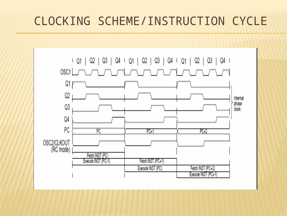
CLOCKING SCHEME/INSTRUCTION CYCLE

INSTRUCTION FLOW/PIPELINING

PROGRAM MEMORY MAP & STACK The PIC16C74 family
has a 13-bit program counter capable of addressing an 4K x 14 (0000h-0FFFh) program memory space.
Accessing a location above the physically implemented address will cause a wraparound.
The reset vector is at 0000h and the interrupt vector is at 0004h.

DATA MEMORY ORGANIZATION
The data memory is partitioned into multiple banks which contain General Purpose Registers Special Function Registers.
Bits RP1 and RP0 are the bank select bits.
RP1:RP0 (STATUS<6:5>) = 00 ® Bank0 = 01 ® Bank1 = 10 ® Bank2 = 11 ® Bank3
Each bank extends up to 7Fh (128 bytes). The lower locations of each bank are reserved for the Special Function Registers. Above the Special Function Registers are General Purpose Registers, implemented as static RAM. All implemented banks contain special function registers. Some “high use” special function registers from one bank may be mirrored in another bank for code reduction and quicker access.

REGISTER FILE
GENERAL PURPOSE REGISTER FILEThe register file can be accessed either directly,
or indirectly through the File Select Register FSR
SPECIAL FUNCTION REGISTERSThe Special Function Registers are registers
used by the CPU and Peripheral Modules for controlling the desired operation of the device. These registers are implemented as static RAM.
The special function registers can be classified into two sets (core and peripheral).

GENERAL PURPOSE REGISTER

SPECIAL FUNCTION REGISTER

STATUS REGISTER

OTHER REGISTERS IN PIC 16C74
Option register INTCON register PIE1 & 2 register PIR1 & 2 register

I/O PORTS Pins for these I/O ports are multiplexed with an
alternate function for the peripheral features on the device.
In general, when a peripheral is enabled, that pin may not be used as a general purpose I/O pin

ADVANTAGES
Small instruction set to learn RISC architecture Built in oscillator with selectable speeds Easy entry level, in circuit programming plus in
circuit debugging PICK it units available for less than $50
Inexpensive microcontrollers Wide range of interfaces including I²C, SPI,
USB, USART, A/D, programmable comparators, PWM, LIN, CAN, PSP, and Ethernet

LIMITATIONS
The PIC architectures have only one accumulator.
Register-bank switching is required to access the entire RAM of many devices
Operations and registers are not orthogonal; some instructions can address RAM and/or immediate constants, while others can only use the accumulator

THANK YOU


![Pic microcontroller [autosaved] [autosaved]](https://img.pdfslide.us/doc/110x75/547c27a4b37959582b8b4f25/pic-microcontroller-autosaved-autosaved.jpg)