Embed Size (px)
Citation preview

Document Number DS40129 Rev 1-2
PI7C9X7952 PCI Express
® Dual UART
Datasheet Revision 1.8
August 2017
1545 Barber Lane Milpitas, CA 95035
Telephone: 408-232-9100
FAX: 408-435-1100
Internet: http://www.diodes.com

Page 2 of 69
PI7C9X7952 www.diodes.com August 2017
Document Number D40129 Rev 1-2 © Diodes Incorporated
All trademarks are property of their respective owners.
PI7C9X7952
IMPORTANT NOTICE DIODES INCORPORATED MAKES NO WARRANTY OF ANY KIND, EXPRESS OR IMPLIED, WITH REGARDS TO THIS DOCUMENT, INCLUDING, BUT NOT LIMITED TO, THE IMPLIED WARRANTIES OF MERCHANTABILITY AND FITNESS FOR A PARTICULAR PURPOSE (AND THEIR EQUIVALENTS UNDER THE LAWS OF ANY JURISDICTION). Diodes Incorporated and its subsidiaries reserve the right to make modifications, enhancements, improvements, corrections or other changes without further notice to this document and any product described herein. Diodes Incorporated does not assume any liability arising out of the application or use of this document or any product described herein; neither does Diodes Incorporated convey any license under its patent or trademark rights, nor the rights of others. Any Customer or user of this document or products described herein in such applications shall assume all risks of such use and will agree to hold Diodes Incorporated and all the companies whose products are represented on Diodes Incorporated website, harmless against all damages. Diodes Incorporated does not warrant or accept any liability whatsoever in respect of any products purchased through unauthorized sales channel. Should Customers purchase or use Diodes Incorporated products for any unintended or unauthorized application, Customers shall indemnify and hold Diodes Incorporated and its representatives harmless against all claims, damages, expenses, and attorney fees arising out of, directly or indirectly, any claim of personal injury or death associated with such unintended or unauthorized application. Products described herein may be covered by one or more United States, international or foreign patents pending. Product names and markings noted herein may also be covered by one or more United States, international or foreign trademarks. This document is written in English but may be translated into multiple languages for reference. Only the English version of this document is the final and determinative format released by Diodes Incorporated.
LIFE SUPPORT
Diodes Incorporated products are specifically not authorized for use as critical components in life support devices or systems without the express written approval of the Chief Executive Officer of Diodes Incorporated. As used herein: A. Life support devices or systems are devices or systems which:
1. are intended to implant into the body, or
2. support or sustain life and whose failure to perform when properly used in accordance with instructions for use provided in the labeling can be reasonably expected to result in significant injury to the user.
B. A critical component is any component in a life support device or system whose failure to perform can be reasonably expected to cause the failure of the life support device or to affect its safety or effectiveness. Customers represent that they have all necessary expertise in the safety and regulatory ramifications of their life support devices or systems, and acknowledge and agree that they are solely responsible for all legal, regulatory and safety-related requirements concerning their products and any use of Diodes Incorporated products in such safety-critical, life support devices or systems, notwithstanding any devices- or systems-related information or support that may be provided by Diodes Incorporated. Further, Customers must fully indemnify Diodes Incorporated and its representatives against any damages arising out of the use of Diodes Incorporated products in such safety-critical, life support devices or systems. Copyright © 2016, Diodes Incorporated
www.diodes.com
Page 3 of 69
PI7C9X7952 www.diodes.com August 2017
Document Number D40129 Rev 1-2 © Diodes Incorporated
All trademarks are property of their respective owners.
PI7C9X7952
REVISION HISTORY
Date Revision Number Description
10/31/07 0.1 Preliminary Datasheet Fixed the diagrams
Corrected Section 4.2 Pin Description (RREF, GPIO[7])
Updated Section PCI Express Registers(6.2.42 [3], 6.2.36 UART Driver Setting, 6.2.41 GPIO Control Register )
Revised Section 7.1 Registers in I/O Mode
Updated Section 11 Ordering Info
12/28/07 0.2 Updated Section 4 Pin Assignment (description for shared pins added, MODE_SEL changed to
DRIVER_SEL, VAUX changed to VDDCAUX)
Updated Section 6 PCI Express Register Description (B4h, D0h) Updated Section 7 UART Register Description
Updated Section 8 EEPROM Interface
04/22/08 0.3 Updated 1 Features (Clock prescaler, Data frame size, Power Dissipation)
Corrected 3 General Description Updated 4 Pin Assignment (description for shared pins added, MODE_SEL changed to DRIVER_SEL,
VAUX changed to VDDCAUX, WAKEUP_L, CLKINP, CLKINN)
Added 5.2.4 Mode Selection, 5.2.5 450/550 Mode, 5.2.6 Enhanced 550 Mode, 5.2.7 Enhanced 950 Mode Corrected 5.2.8 Transmit and Receive FIFOs, 5.2.9 Automated Flow Control
Modified 5.2.12 Baud Rate Generation
Updated Section 6 PCI Express Register Description (6.2.36, 6.2.42) Updated Format (6.2.20, 6.2.36, 6.2.54, 6.2.55, 6.2.57)
Updated Section 7 UART Register Description (7.1.6 LCR Bit[5:0], 7.1.7 MCR Bit[5] and Bit[7], 7.1.9
MSR Bit[3:0], 7.2.6 LCR Bit[5:0], 7.2.7 MCR Bit[5] and Bit[7], 7.2.9 MSR Bit[3:0], 7.2.11 DLL, 7.2.12 DLH, 7.2.13 EFR, 7.2.18 ACR Bit[7:2], 7.2.23 CPRM)
Updated Section 8.3 EEPROM Space Address Map And Description (00h, 0Ah, 40h)
Added Section 9 Electrical Specification Corrected Section 9.2 DC Specification
Updated Section 9.3 AC Specification
Added Section 10 Clock Scheme
08/13/08 0.4 Updated Section 1 Features (added Industrial Temperature Range)
Updated Section 9.1 Absolute Maximum Ratings: Ambient Temperature with power applied
11/25/08 1.0 Updated Section 7.1.13 Sample Clock Register and 7.2.27 Sample Clock Register Updated Section 12 Ordering Information
Removed “Preliminary” and “Confidential” references
03/06/09 1.1 Corrected Figure 3.1 PI7C9X7952 Block Diagram (SYN_UART_CLK removed)
Corrected Section 4.2.1 UART Interface (SYNCLK_IN_EN and SYN_UART_CLK removed) Corrected Figure 5.2 Internal Loopback in PI7C7952
Corrected Figure 5.3 Crystal Oscillator as the Clock Source (14.7456 MHz)
Corrected Section 7.1.7 Modem Control Register (Bit[5]), 7.1.10 Special Function Register (Bit[4]), 7.2.7 Modem Control Register (Bit[5]), 7.2.10 Special Function Register (Bit[4]), 7.2.29 Receive FIFO Data
Registers, 7.2.30 Transmit FIFO Data Register, 7.2.31
04/21/09 1.2 Updated Section 4.2 Pin Description
09/24/09 1.3 Updated Figure 5-3 Crystal Oscillator as the Clock Source Updated Section 6.2.24 Message Signaled Interrupt (MSI) Next Item Pointer 8Ch
Added Section 6.2.25 Message Address Register – Offset 90h
Added Section 6.2.26 Message Upper Address Register – Offset 94h Added Section 6.2.27 Message Data Register – Offset 98h
06/04/14 1.4 Updated Section 4.1 Pin List (SR_DO and SR_DI)
Updated Section 4.2.5 EEPROM Interface (SR_DO and SR_DI) Created for IC Revision B
Updated Section 12 Ordering Information
Added Section 6.2.25 Message Control Register – OFFSET 8Ch
01/09/15 1.5 Updated Section 11 Package Information
05/11/15 1.6 Updated Table 5.2 Baud Rate Generator Setting
Updated Section 7.2.23 Clock Prescale Register –Offset 14h
12/13/16 1.7 Updated Logo Updated Table 9.1 Absolute Maximum Ratings
Updated Table 9.2 DC Electrical Characteristics
08/29/17 1.8 Updated Section 4.1 Pin List of 160-Pin LFBGA
Updated Section 4.2.1 UART Interface Updated Table 9.2 DC Electrical Characteristics
Updated Section 12 Ordering Information
Page 4 of 69
PI7C9X7952 www.diodes.com August 2017
Document Number D40129 Rev 1-2 © Diodes Incorporated
All trademarks are property of their respective owners.
PI7C9X7952
Table of Contents
1. FEATURES ............................................................................................................................................ 9
2. APPLICATIONS ................................................................................................................................... 9
3. GENERAL DESCRIPTION ............................................................................................................... 10
4. PIN ASSIGNMENT ............................................................................................................................. 11
4.1. PIN LIST OF 128-PIN LQFP ......................................................................................................... 11 4.2. PIN DESCRIPTION ...................................................................................................................... 12
4.2.1. UART INTERFACE ................................................................................................................ 12 4.2.2. PCI EXPRESS INTERFACE .................................................................................................. 13 4.2.3. SYSTEM INTERFACE............................................................................................................ 13 4.2.4. TEST SIGNALS ...................................................................................................................... 14 4.2.5. EEPROM INTERFACE .......................................................................................................... 15 4.2.6. POWER PINS ........................................................................................................................ 15
5. FUNCTIONAL DESCRIPTION ........................................................................................................ 16
5.1. CONFIGURATION SPACE .......................................................................................................... 16 5.1.1. PCI Express Configuration Space ......................................................................................... 16 5.1.2. UART Configuration Space ................................................................................................... 16
5.2. DEVICE OPERATION .................................................................................................................. 17 5.2.1. Configuration Access ............................................................................................................. 17 5.2.2. I/O Reads/Writes .................................................................................................................... 17 5.2.3. Memory Reads/Writes ............................................................................................................ 17 5.2.4. Mode Selection ...................................................................................................................... 18 5.2.5. 450/550 Mode ........................................................................................................................ 18 5.2.6. Enhanced 550 Mode .............................................................................................................. 18 5.2.7. Enhanced 950 Mode .............................................................................................................. 18 5.2.8. Transmit and Receive FIFOs ................................................................................................. 18 5.2.9. Automated Flow Control........................................................................................................ 20 5.2.10. Internal Loopback .................................................................................................................. 21 5.2.11. Crystal Oscillator .................................................................................................................. 22 5.2.12. Baud Rate Generation ........................................................................................................... 23 5.2.13. Power Management ............................................................................................................... 23
6. PCI EXPRESS REGISTER DESCRIPTION ................................................................................... 24
6.1. REGISTER TYPES ....................................................................................................................... 24 6.2. CONFIGURATION REGISTERS ................................................................................................. 24
6.2.1. VENDOR ID REGISTER – OFFSET 00h .............................................................................. 25 6.2.2. DEVICE ID REGISTER – OFFSET 00h................................................................................ 25 6.2.3. COMMAND REGISTER – OFFSET 04h ............................................................................... 25 6.2.4. STATUS REGISTER – OFFSET 04h ...................................................................................... 25 6.2.5. REVISION ID REGISTER – OFFSET 08h ............................................................................ 26 6.2.6. CLASS CODE REGISTER – OFFSET 08h ............................................................................ 26 6.2.7. CACHE LINE REGISTER – OFFSET 0Ch............................................................................ 26 6.2.8. MASTER LATENCY TIMER REGISTER – OFFSET 0Ch ..................................................... 27 6.2.9. HEADER TYPE REGISTER – OFFSET 0Ch......................................................................... 27 6.2.10. BASE ADDRESS REGISTER 0 – OFFSET 10h ..................................................................... 27 6.2.11. BASE ADDRESS REGISTER 1 – OFFSET 14h ..................................................................... 27 6.2.12. SUBSYSTEM VENDOR REGISTER – OFFSET 2Ch ............................................................ 27
Page 5 of 69
PI7C9X7952 www.diodes.com August 2017
Document Number D40129 Rev 1-2 © Diodes Incorporated
All trademarks are property of their respective owners.
PI7C9X7952
6.2.13. SUBSYSTEM ID REGISTER – OFFSET 2Ch ........................................................................ 27 6.2.14. CAPABILITIES POINTER REGISTER – OFFSET 34h ......................................................... 27 6.2.15. INTERRUPT LINE REGISTER – OFFSET 3Ch .................................................................... 27 6.2.16. INTERRUPT PIN REGISTER – OFFSET 3Ch ...................................................................... 28 6.2.17. POWER MANAGEMENT CAPABILITY ID REGISTER – OFFSET 80h ............................... 28 6.2.18. NEXT ITEM POINTER REGISTER – OFFSET 80h .............................................................. 28 6.2.19. POWER MANAGEMENT CAPABILITIES REGISTER – OFFSET 80h ................................ 28 6.2.20. POWER MANAGEMENT DATA REGISTER – OFFSET 84h ............................................... 28 6.2.21. PPB SUPPORT EXTENSIONS – OFFSET 84h ..................................................................... 29 6.2.22. PM DATA REGISTER – OFFSET 84h ................................................................................... 29 6.2.23. MESSAGE SIGNALED INTERRUPTS (MSI) Capability ID Register 8Ch ........................... 29 6.2.24. MESSAGE SIGNALED INTERRUPTS (MSI) NEXT ITEM POINTER 8Ch .......................... 29 6.2.25. MESSAGE CONTROL REGISTER – OFFSET 8Ch .............................................................. 29 6.2.26. MESSAGE ADDRESS REGISTER – OFFSET 90h ............................................................... 30 6.2.27. MESSAGE UPPER ADDRESS REGISTER – OFFSET 94h .................................................. 30 6.2.28. MESSAGE DATA REGISTER – OFFSET 98h ....................................................................... 30 6.2.29. VPD CAPABILITY ID REGISTER – OFFSET 9Ch ............................................................... 30 6.2.30. NEXT ITEM POINTER REGISTER – OFFSET 9Ch ............................................................. 30 6.2.31. VPD REGISTER – OFFSET 9Ch .......................................................................................... 30 6.2.32. VPD DATA REGISTER – OFFSET A0h ................................................................................ 31 6.2.33. VENDOR SPECIFIC CAPABILITY ID REGISTER – OFFSET A4h ..................................... 31 6.2.34. NEXT ITEM POINTER REGISTER – OFFSET A4h ............................................................. 31 6.2.35. LENGTH REGISTER – OFFSET A4h ................................................................................... 31 6.2.36. XPIP CSR0 – OFFSET A8h (Test Purpose Only) .................................................................. 31 6.2.37. XPIP CSR1 – OFFSET ACh (Test Purpose Only).................................................................. 31 6.2.38. REPLAY TIME-OUT COUNTER – OFFSET B0h ................................................................. 32 6.2.39. ACKNOWLEDGE LATENCY TIMER – OFFSET B0h .......................................................... 32 6.2.40. UART DRIVE SETTING – OFFSET B4h............................................................................... 32 6.2.41. POWER MANAGEMENT CONTROL PARAMETER – OFFSET B8h ................................... 32 6.2.42. DEBUG REGISTER 1 – OFFSET BCh (Test Purpose Only) ................................................ 33 6.2.43. DEBUG REGISTER 2 – OFFSET C0h (Test Purpose Only) ................................................. 33 6.2.44. DEBUG REGISTER 3 – OFFSET C4h (Test Purpose Only) ................................................. 33 6.2.45. DEBUG REGISTER 4 – OFFSET C8h (Test Purpose Only) ................................................. 33 6.2.46. GPIO CONTROL REGISTER – OFFSET D8h ...................................................................... 33 6.2.47. EEPROM CONTROL REGISTER – OFFSET DCh ............................................................... 34 6.2.48. PCI EXPRESS CAPABILITY ID REGISTER – OFFSET E0h ................................................ 34 6.2.49. NEXT ITEM POINTER REGISTER – OFFSET E0h ............................................................. 34 6.2.50. PCI EXPRESS CAPABILITIES REGISTER – OFFSET E0h ................................................. 34 6.2.51. DEVICE CAPABILITIES REGISTER – OFFSET E4h ........................................................... 34 6.2.52. DEVICE CONTROL REGISTER – OFFSET E8h ................................................................. 35 6.2.53. DEVICE STATUS REGISTER – OFFSET E8h ...................................................................... 36 6.2.54. LINK CAPABILITIES REGISTER – OFFSET ECh ............................................................... 36 6.2.55. LINK CONTROL REGISTER – OFFSET F0h ....................................................................... 37 6.2.56. LINK STATUS REGISTER – OFFSET F0h ........................................................................... 37 6.2.57. PCI EXPRESS ADVANCED ERROR REPORTING CAPABILITY ID REGISTER – OFFSET
100h 38 6.2.58. CAPABILITY VERSION – OFFSET 100h .............................................................................. 38 6.2.59. NEXT ITEM POINTER REGISTER – OFFSET 100h ............................................................ 38 6.2.60. UNCORRECTABLE ERROR STATUS REGISTER – OFFSET 104h ..................................... 38 6.2.61. UNCORRECTABLE ERROR MASK REGISTER – OFFSET 108h........................................ 39 6.2.62. UNCORRECTABLE ERROR SEVERITY REGISTER – OFFSET 10Ch ................................ 40 6.2.63. CORRECTABLE ERROR STATUS REGISTER – OFFSET 110h........................................... 41

Page 6 of 69
PI7C9X7952 www.diodes.com August 2017
Document Number D40129 Rev 1-2 © Diodes Incorporated
All trademarks are property of their respective owners.
PI7C9X7952
6.2.64. CORRECTABLE ERROR MASK REGISTER – OFFSET 114h ............................................. 41 6.2.65. ADVANCE ERROR CAPABILITIES AND CONTROL REGISTER – OFFSET 118h ............. 42 6.2.66. HEADER LOG REGISTER – OFFSET From 11Ch to 128h ................................................. 42
7. UART REGISTER DESCRIPTION .................................................................................................. 43
7.1. REGISTERS IN I/O MODE .......................................................................................................... 43 7.1.1. RECEIVE HOLDING REGISTER – OFFSET 00h ................................................................ 44 7.1.2. TRANSMIT HOLDING REGISTER – OFFSET 00h .............................................................. 44 7.1.3. INTERRUPT ENABLE REGISTER – OFFSET 01h .............................................................. 44 7.1.4. INTERRUPT STATUS REGISTER – OFFSET 02h ................................................................ 45 7.1.5. FIFO CONTROL REGISTER – OFFSET 02h ....................................................................... 45 7.1.6. LINE CONTROL REGISTER – OFFSET 03h ....................................................................... 46 7.1.7. MODEM CONTROL REGISTER – OFFSET 04h ................................................................. 46 7.1.8. LINE STATUS REGISTER – OFFSET 05h ............................................................................ 47 7.1.9. MODEM STATUS REGISTER – OFFSET 06h ...................................................................... 48 7.1.10. SPECIAL FUNCTION REGISTER – OFFSET 07h ............................................................... 48 7.1.11. DIVISOR LATCH LOW REGISTER – OFFSET 00h, LCR[7] = 1 ........................................ 49 7.1.12. DIVISOR LATCH HIGH REGISTER – OFFSET 01h, LCR[7] = 1....................................... 49 7.1.13. SAMPLE CLOCK REGISTER – OFFSET 02h, LCR[7] = 1 ................................................. 49
7.2. REGISTERS IN MEMORY-MAPPING MODE ........................................................................... 50 7.2.1. RECEIVE HOLDING REGISTER – OFFSET 00h ................................................................ 51 7.2.2. TRANSMIT HOLDING REGISTER – OFFSET 00h .............................................................. 52 7.2.3. INTERRUPT ENABLE REGISTER – OFFSET 01h .............................................................. 52 7.2.4. INTERRUPT STATUS REGISTER – OFFSET 02h ................................................................ 52 7.2.5. FIFO CONTROL REGISTER – OFFSET 02h ....................................................................... 53 7.2.6. LINE CONTROL REGISTER – OFFSET 03h ....................................................................... 53 7.2.7. MODEM CONTROL REGISTER – OFFSET 04h ................................................................. 54 7.2.8. LINE STATUS REGISTER – OFFSET 05h ............................................................................ 55 7.2.9. MODEM STATUS REGISTER – OFFSET 06h ...................................................................... 55 7.2.10. SPECIAL FUNCTION REGISTER – OFFSET 07h ............................................................... 56 7.2.11. DIVISOR LATCH LOW REGISTER – OFFSET 08h ............................................................. 56 7.2.12. DIVISOR LATCH HIGH REGISTER – OFFSET 09h............................................................ 56 7.2.13. ENHANCED FUNCTION REGISTER – OFFSET 0Ah ......................................................... 57 7.2.14. XON SPECIAL CHARACTER 1 – OFFSET 0Bh ................................................................... 58 7.2.15. XON SPECIAL CHARACTER 2 – OFFSET 0Ch .................................................................. 58 7.2.16. XOFF SPECIAL CHARACTER 1 – OFFSET 0Dh ................................................................ 58 7.2.17. XOFF SPECIAL CHARACTER 2 – OFFSET 0Eh................................................................. 58 7.2.18. ADVANCE CONTROL REGISTER – OFFSET 0Fh .............................................................. 58 7.2.19. TRANSMIT INTERRUPT TRIGGER LEVEL – OFFSET 10h ............................................... 59 7.2.20. RECEIVE INTERRUPT TRIGGER LEVEL – OFFSET 11h .................................................. 59 7.2.21. FLOW CONTROL LOW TRIGGER LEVEL – OFFSET 12h ................................................. 59 7.2.22. FLOW CONTROL HIGH TRIGGER LEVEL – OFFSET 13h ............................................... 59 7.2.23. CLOCK PRESCALE REGISTER – OFFSET 14h .................................................................. 59 7.2.24. RECEIVE FIFO DATA COUNTER – OFFSET 15h, SFR[6] = 0 .......................................... 60 7.2.25. LINE STATUS REGISTER COUNTER – OFFSET 15h, SFR[6] = 1 .................................... 60 7.2.26. TRANSMIT FIFO DATA COUNTER – OFFSET 16h, SFR[7] = 1 ....................................... 60 7.2.27. SAMPLE CLOCK REGISTER – OFFSET 16h, SFR[7] = 0 ................................................. 60 7.2.28. GLOBAL LINE STATUS REGISTER – OFFSET 17h ............................................................ 61 7.2.29. RECEIVE FIFO DATA REGISTERS – OFFSET 100h ~ 17Fh .............................................. 61 7.2.30. TRANSMIT FIFO DATA REGISTERS – OFFSET 100h ~ 17Fh ........................................... 61 7.2.31. LINE STATUS FIFO REGISTERS –OFFSET 180h ~ 1FFh .................................................. 61
8. EEPROM INTERFACE ..................................................................................................................... 62
Page 7 of 69
PI7C9X7952 www.diodes.com August 2017
Document Number D40129 Rev 1-2 © Diodes Incorporated
All trademarks are property of their respective owners.
PI7C9X7952
8.1. AUTO MODE EERPOM ACCESS ............................................................................................... 62 8.2. EEPROM MODE AT RESET ........................................................................................................ 62 8.3. EEPROM SPACE ADDRESS MAP AND DESCRIPTION .......................................................... 62
9. ELECTRICAL SPECIFICATION ..................................................................................................... 64
9.1. ABSOLUTE MAXIMUM RATINGS ........................................................................................... 64 9.2. DC SPECIFICATIONS .................................................................................................................. 64 9.3. AC SPECIFICATIONS .................................................................................................................. 64
10. CLOCK SCHEME .......................................................................................................................... 67
11. PACKAGE INFORMATION ......................................................................................................... 68
12. ORDER INFORMATION .............................................................................................................. 69
Page 8 of 69
PI7C9X7952 www.diodes.com August 2017
Document Number D40129 Rev 1-2 © Diodes Incorporated
All trademarks are property of their respective owners.
PI7C9X7952
Table of Tables
TABLE 4-1 PIN-LIST OF 128-PIN LQFP ........................................................................................................... 11 TABLE 5-1 MODE SELECTION ......................................................................................................................... 18 TABLE 5-2 BAUD RATE GENERATOR SETTING ................................................................................................ 23 TABLE 5-3 SAMPLE BAUD RATE SETTING ....................................................................................................... 23 TABLE 7-1 UART BASE ADDRESS IN I/O MODE ............................................................................................. 43 TABLE 7-2 REGISTERS IN I/O MODE ............................................................................................................... 44 TABLE 7-3 UART BASE ADDRESS IN MEMORY MODE.................................................................................... 50 TABLE 7-4 MEMORY-MAP MODE ................................................................................................................... 51 TABLE 9-1 ABSOLUTE MAXIMUM RATINGS .................................................................................................... 64 TABLE 9-2 DC ELECTRICAL CHARACTERISTICS ............................................................................................. 64 TABLE 9-3 TRANSMITTER CHARACTERISTICS ................................................................................................. 64 TABLE 9-4 RECEIVER CHARACTERISTICS ....................................................................................................... 65 TABLE 10-1 INPUT CLOCK REQUIREMENTS .................................................................................................... 67
List of Figures
FIGURE 3-1 PI7C9X7952 BLOCK DIAGRAM................................................................................................... 10 FIGURE 5-1 TRANSMIT AND RECEIVE FIFOS .................................................................................................. 19 FIGURE 5-2 INTERNAL LOOPBACK IN PI7C9X7952 ........................................................................................ 21 FIGURE 5-3 CRYSTAL OSCILLATOR AS THE CLOCK SOURCE ........................................................................... 22 FIGURE 5-4 EXTERNAL CLOCK SOURCE AS THE CLOCK SOURCE .................................................................... 22 FIGURE 7-1 UART REGISTER BLOCK ARRANGEMENT IN I/O MODE .............................................................. 43 FIGURE 7-2 UART REGISTER BLOCK ARRANGEMENT IN MEMORY MODE ..................................................... 50 FIGURE 11-1 PACKAGE OUTLINE DRAWING .................................................................................................... 68

Page 9 of 69
PI7C9X7952 www.diodes.com August 2017
Document Number D40129 Rev 1-2 © Diodes Incorporated
All trademarks are property of their respective owners.
PI7C9X7952
1. FEATURES
x1 PCI Express link host interface
Dual high performance 950-class UARTs
Compliant with PCI Express Base Specification 1.1
Compliant with PCI Express CEM Specification 1.1
Compliant with PCI Power Management 1.2
Fully 16C550 software compatible UARTs
128-byte FIFO for each transmitter and receiver
Baud rate up to 15 Mbps in asynchronous mode
Flexible clock prescaler from 4 to 46
Automated in-band flow control using programmable Xon/Xoff in both directions
Automated out-of-band flow control using CTS#/RTS# and/or DSR#/DTR#
Arbitrary trigger levels for receiver and transmitter FIFO interrupts and automatic in-band and
out-of-band flow control
Global Interrupt Status and readable FIFO levels to facilitate implementation of efficient device
drivers
Detection of bad data in the receiver FIFO
Data framing size including 5, 6, 7, 8 and 9 bits
Hardware reconfiguration through Microwire compatible EEPROM
Operations via I/O or memory mapping
Dual power operation (1.8V for PCIe I/O and core, 3.3V for UART I/O)
Power dissipation: 0.7 W typical in normal mode
Industrial Temperature Range -40o to 85
o
128-pin LQFP, Pb-free and 100% Green
2. APPLICATIONS
Remote Access Servers
Network / Storage Management
Factory Automation and Process Control
Instrumentation
Multi-port RS-232/ RS-422/ RS-485 Cards
Point-of-Sale Systems (PoS)
Industrial PC (IPC)
Industrial Control
Gaming Machines
Building Automation
Embedded Systems
Page 10 of 69
PI7C9X7952 www.diodes.com August 2017
Document Number D40129 Rev 1-2 © Diodes Incorporated
All trademarks are property of their respective owners.
PI7C9X7952
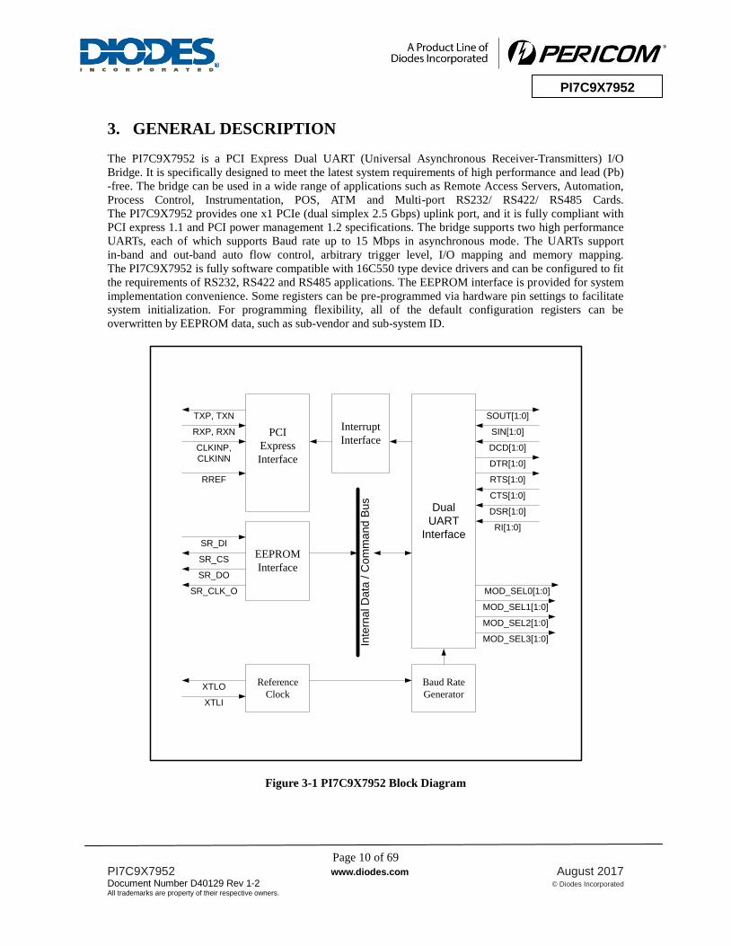
3. GENERAL DESCRIPTION
The PI7C9X7952 is a PCI Express Dual UART (Universal Asynchronous Receiver-Transmitters) I/O
Bridge. It is specifically designed to meet the latest system requirements of high performance and lead (Pb)
-free. The bridge can be used in a wide range of applications such as Remote Access Servers, Automation,
Process Control, Instrumentation, POS, ATM and Multi-port RS232/ RS422/ RS485 Cards.
The PI7C9X7952 provides one x1 PCIe (dual simplex 2.5 Gbps) uplink port, and it is fully compliant with
PCI express 1.1 and PCI power management 1.2 specifications. The bridge supports two high performance
UARTs, each of which supports Baud rate up to 15 Mbps in asynchronous mode. The UARTs support
in-band and out-band auto flow control, arbitrary trigger level, I/O mapping and memory mapping.
The PI7C9X7952 is fully software compatible with 16C550 type device drivers and can be configured to fit
the requirements of RS232, RS422 and RS485 applications. The EEPROM interface is provided for system
implementation convenience. Some registers can be pre-programmed via hardware pin settings to facilitate
system initialization. For programming flexibility, all of the default configuration registers can be
overwritten by EEPROM data, such as sub-vendor and sub-system ID.
PCI
Express
Interface
Dual
UART
Interface
SOUT[1:0]
SIN[1:0]
DCD[1:0]
DTR[1:0]
RTS[1:0]
CTS[1:0]
DSR[1:0]
RI[1:0]
XTLO
XTLI
MOD_SEL0[1:0]
MOD_SEL1[1:0]
MOD_SEL2[1:0]
MOD_SEL3[1:0]Inte
rna
l D
ata
/ C
om
ma
nd
Bu
s
TXP, TXN
RXP, RXN
CLKINP,
CLKINN
RREF
EEPROM
Interface
SR_DI
SR_CS
SR_DO
SR_CLK_O
Interrupt
Interface
Reference
Clock
Baud Rate
Generator
Figure 3-1 PI7C9X7952 Block Diagram
Page 11 of 69
PI7C9X7952 www.diodes.com August 2017
Document Number D40129 Rev 1-2 © Diodes Incorporated
All trademarks are property of their respective owners.
PI7C9X7952
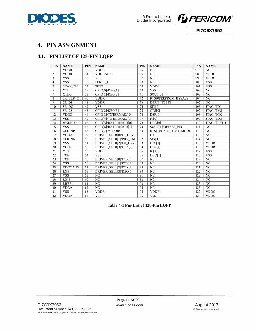
4. PIN ASSIGNMENT
4.1. PIN LIST OF 128-PIN LQFP
PIN NAME PIN NAME PIN NAME PIN NAME
1 VDDR 33 VDDC 65 NC 97 NC
2 VDDR 34 VDDCAUX 66 NC 98 VDDC
3 VSS 35 VSS 67 NC 99 VDDC
4 VSS 36 PERST_L 68 NC 100 VSS
5 SCAN_EN 37 TEST 69 VDDC 101 VSS
6 XTLI 38 GPIO[0]/DEQ[1] 70 VSS 102 NC
7 XTLO 39 GPIO[1]/DEQ[2] 71 SOUT[0] 103 NC
8 SR_CLK_O 40 VDDR 72 RTS[0]/EEPROM_BYPASS 104 NC
9 SR_DI 41 VDDR 73 DTR[0]/TEST2 105 NC
10 SR_DO 42 VSS 74 SIN[0] 106 JTAG_TDI
11 SR_CS 43 GPIO[2]/DEQ[3] 75 CTS[0] 107 JTAG_TMS
12 VDDC 44 GPIO[3]/TXTERMADJ[0] 76 DSR[0] 108 JTAG_TCK
13 VSS 45 GPIO[4]/TXTERMADJ[1] 77 RI[0] 109 JTAG_TDO
14 WAKEUP_L 46 GPIO[5]/RXTERMADJ[0] 78 DCD[0] 110 JTAG_TRST_L
15 VSS 47 GPIO[6]/RXTERMADJ[1] 79 SOUT[1]/DEBUG_PIN 111 NC
16 CLKINP 48 GPIO[7] /SR_ORG 80 RTS[1]/UART_TEST_MODE 112 NC
17 VDDA 49 DRIVER_SEL0[0]/HI_DRV 81 DTR[1] 113 NC
18 CLKINN 50 DRIVER_SEL0[1]/PHY_TM 82 SIN[1] 114 NC
19 VSS 51 DRIVER_SEL0[2]/LO_DRV 83 CTS[1] 115 VDDR
20 VDDC 52 DRIVER_SEL0[3]/DTX[0] 84 DSR[1] 116 VDDR
21 VTT 53 VDDC 85 RI[1] 117 VSS
22 TXN 54 VSS 86 DCD[1] 118 VSS
23 TXP 55 DRIVER_SEL1[0]/DTX[1] 87 NC 119 NC
24 VSS 56 DRIVER_SEL1[1]/DTX[2] 88 NC 120 NC
25 VDDCAUX 57 DRIVER_SEL1[2]/DTX[3] 89 NC 121 NC
26 RXP 58 DRIVER_SEL1[3]/DEQ[0] 90 NC 122 NC
27 VSS 59 NC 91 NC 123 NC
28 RXN 60 NC 92 NC 124 NC
29 RREF 61 NC 93 NC 125 NC
30 VDDA 62 NC 94 NC 126 NC
31 VSS 63 VDDR 95 VDDR 127 VDDC
32 VDDA 64 VSS 96 VSS 128 VDDC
Table 4-1 Pin-List of 128-Pin LQFP
Page 12 of 69
PI7C9X7952 www.diodes.com August 2017
Document Number D40129 Rev 1-2 © Diodes Incorporated
All trademarks are property of their respective owners.
PI7C9X7952
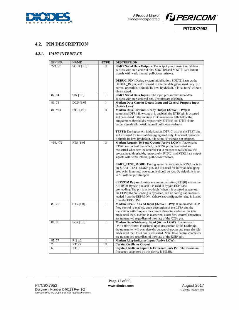
4.2. PIN DESCRIPTION
4.2.1. UART INTERFACE
PIN NO. NAME TYPE DESCRIPTION
*79, 71 SOUT [1:0] O UART Serial Data Outputs: The output pins transmit serial data
packets with start and end bits. SOUT[0] and SOUT[1] are output signals with weak internal pull-down resistors.
DEBUG_PIN: During system initialization, SOUT[1] acts as the DEBUG_IN pin, and it is used to internal debugging used only. In
normal operation, it should be low. By default, it is set to ‘0’ without
pin strapped.
82, 74 SIN [1:0] I UART Serial Data Inputs: The input pins receive serial data
packets with start and end bits. The pins are idle high.
86, 78 DCD [1:0] I Modem Data-Carrier-Detect Input and General Purpose Input
(Active Low)
81, *73 DTR [1:0] O Modem Data-Terminal-Ready Output (Active LOW): If
automated DTR# flow control is enabled, the DTR# pin is asserted
and deasserted if the receiver FIFO reaches or falls below the programmed thresholds, respectively. DTR[0] and DTR[1] are
output signals with weak internal pull-down resistors.
TEST2: During system initialization, DTR[0] acts as the TEST pin,
and it is used for internal debugging used only. In normal operation,
it should be low. By default, it is set to ‘0’ without pin strapped.
*80, *72 RTS [1:0] O Modem Request-To-Send Output (Active LOW): If automated RTS# flow control is enabled, the RTS# pin is deasserted and
reasserted whenever the receiver FIFO reaches or falls below the
programmed thresholds, respectively. RTS[0] and RTS[1] are output signals with weak internal pull-down resistors.
UART_TEST_MODE: During system initialization, RTS[1] acts as the UART_TEST_MODE pin, and it is used for internal debugging
used only. In normal operation, it should be low. By default, it is set
to ‘0’ without pin strapped.
EEPROM Bypass: During system initialization, RTS[0] acts as the EEPROM Bypass pin, and it is used to bypass EEPROM
pre-loading. The pin is active-high. When it is asserted at start-up,
the EEPROM pre-loading is bypassed, and no configuration data is loaded from the EEPRPOM. Otherwise, configuration data is loaded
from the EEPROM.
83, 75 CTS [1:0] I Modem Clear-To-Send Input (Active LOW): If automated CTS#
flow control is enabled, upon deassertion of the CTS# pin, the transmitter will complete the current character and enter the idle
mode until the CTS# pin is reasserted. Note: flow control characters
are transmitted regardless of the state of the CTS# pin.
84, 76 DSR [1:0] I Modem Data-Set-Ready Input (Active LOW): If automated
DSR# flow control is enabled, upon deassertion of the DSR# pin,
the transmitter will complete the current character and enter the idle mode until the DSR# pin is reasserted. Note: flow control characters
are transmitted regardless of the state of the DSR# pin.
85, 77 RI [1:0] I Modem Ring-Indicator Input (Active LOW)
7 XTLO O Crystal Oscillator Output
6 XTLI I Crystal Oscillator Input Or External Clock Pin: The maximum frequency supported by this device is 60MHz.

Page 13 of 69
PI7C9X7952 www.diodes.com August 2017
Document Number D40129 Rev 1-2 © Diodes Incorporated
All trademarks are property of their respective owners.
PI7C9X7952
PIN NO. NAME TYPE DESCRIPTION
*52, *51,
*50, *49
DRIVER_SEL0
[3:0]
O DRIVER_SEL0: Used to select RS-232/ RS-424/ 4-Wire RS-485/
2-Wire RS-458 Serial Port Mode for UART 0. DRIVER_SEL0 [3:0]
are output signals with weak internal pull-down resistors.
Driver Current Level Control (DTX[0]): During system
initialization, DRIVER_SEL0[3] acts as the DTX[0] pin, and it is used to control the driver current level. By default, it is set to ‘0’
without pin strapped.
Low Driver Control (LO_DRV): During system initialization,
DRIVER_SEL0[2] acts as the LO_DRV pin, and it is used to
decrease the nominal value of the PCI Express lane’s driver current level. By default, it is set to ‘0’ without pin strapped.
PHY_TM: During system initialization, DRIVER_SEL0[1] acts as the PHY_TM pin, and it is used for internal debugging used only. In
normal operation, it should be low. By default, it is set to ‘0’ without
pin strapped.
High Driver Control (HI_DRV): During system initialization,
DRIVER_SEL0[0] acts as the HI_DRV pin, and it is used to increase the nominal value of the PCI Express lane’s driver current
level. By default, it is set ‘0’ without pin strapped.
*58, *57, *56, *55
DRIVER_SEL1 [3:0]
O DRIVER_SEL1: Used to select RS-232/ RS-424/ 4-Wire RS-485/ 2-Wire RS-458 Serial Port Mode for UART 1.
Driver Equalization Level Control (DEQ[0]): During system initialization, DRIVER_SEL1[3] acts as the DEQ[0] pin, and it is
used to control the driver current level. By default, it is set to ‘0’
without pin strapped.
Driver Current Level Control (DTX[3:1]): During system
initialization, DRIVER_SEL1[2:0] acts as the DTX[3:1] pins, and they are used to control the driver current level. By default, they are
set to ‘000’ without pin strapped.
4.2.2. PCI EXPRESS INTERFACE
PIN NO. NAME TYPE DESCRIPTION
23, 22 TXP, TXN O PCI Express Serial Output Signal: Differential PCI Express
output signals.
26, 28 RXP, RXN I PCI Express Serial Input Signal: Differential PCI Express input
signals.
16, 18 CLKINP,
CLKINN
I Reference Input Clock: Connects to external 100MHz differential
clock
The input clock signals must be delivered to the clock buffer cell
through an AC-coupled interface so that only the AC information of
the clock is received, converted, and buffered. It is recommended that a 0.1uF be used in the AC-coupling.
29 RREF I Reference Resistor: To accurately set internal bias references, a
precision resistor must be connected between Rref and Vss. The
resistor should have a nominal value of 2.1 KΩ and accuracy of +/- 1%
4.2.3. SYSTEM INTERFACE
PIN NO. NAME TYPE DESCRIPTION
36 PEREST_L I System Reset Input
Page 14 of 69
PI7C9X7952 www.diodes.com August 2017
Document Number D40129 Rev 1-2 © Diodes Incorporated
All trademarks are property of their respective owners.
PI7C9X7952
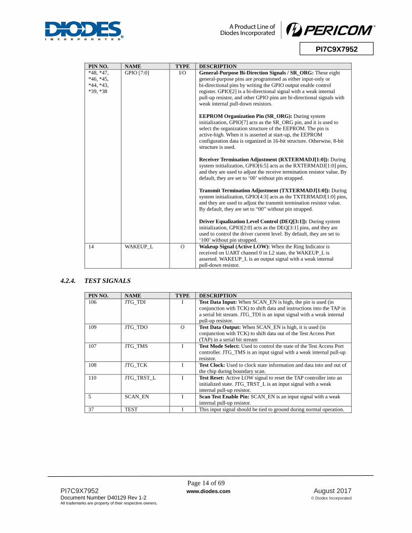
PIN NO. NAME TYPE DESCRIPTION
*48, *47,
*46, *45,
*44, *43, *39, *38
GPIO [7:0] I/O General-Purpose Bi-Direction Signals / SR_ORG: These eight
general-purpose pins are programmed as either input-only or
bi-directional pins by writing the GPIO output enable control register. GPIO[2] is a bi-directional signal with a weak internal
pull-up resistor, and other GPIO pins are bi-directional signals with
weak internal pull-down resistors.
EEPROM Organization Pin (SR_ORG): During system
initialization, GPIO[7] acts as the SR_ORG pin, and it is used to select the organization structure of the EEPROM. The pin is
active-high. When it is asserted at start-up, the EEPROM
configuration data is organized in 16-bit structure. Otherwise, 8-bit structure is used.
Receiver Termination Adjustment (RXTERMADJ[1:0]): During system initialization, GPIO[6:5] acts as the RXTERMADJ[1:0] pins,
and they are used to adjust the receive termination resistor value. By
default, they are set to ‘00’ without pin strapped.
Transmit Termination Adjustment (TXTERMADJ[1:0]): During
system initialization, GPIO[4:3] acts as the TXTERMADJ[1:0] pins, and they are used to adjust the transmit termination resistor value.
By default, they are set to “00” without pin strapped.
Driver Equalization Level Control (DEQ[3:1]): During system
initialization, GPIO[2:0] acts as the DEQ[3:1] pins, and they are
used to control the driver current level. By default, they are set to ‘100’ without pin strapped.
14 WAKEUP_L O Wakeup Signal (Active LOW): When the Ring Indicator is
received on UART channel 0 in L2 state, the WAKEUP_L is asserted. WAKEUP_L is an output signal with a weak internal
pull-down resistor.
4.2.4. TEST SIGNALS
PIN NO. NAME TYPE DESCRIPTION
106 JTG_TDI I Test Data Input: When SCAN_EN is high, the pin is used (in
conjunction with TCK) to shift data and instructions into the TAP in
a serial bit stream. JTG_TDI is an input signal with a weak internal pull-up resistor.
109 JTG_TDO O Test Data Output: When SCAN_EN is high, it is used (in
conjunction with TCK) to shift data out of the Test Access Port
(TAP) in a serial bit stream
107 JTG_TMS I Test Mode Select: Used to control the state of the Test Access Port
controller. JTG_TMS is an input signal with a weak internal pull-up
resistor.
108 JTG_TCK I Test Clock: Used to clock state information and data into and out of the chip during boundary scan.
110 JTG_TRST_L I Test Reset: Active LOW signal to reset the TAP controller into an
initialized state. JTG_TRST_L is an input signal with a weak internal pull-up resistor.
5 SCAN_EN I Scan Test Enable Pin: SCAN_EN is an input signal with a weak
internal pull-up resistor.
37 TEST I This input signal should be tied to ground during normal operation.
Page 15 of 69
PI7C9X7952 www.diodes.com August 2017
Document Number D40129 Rev 1-2 © Diodes Incorporated
All trademarks are property of their respective owners.
PI7C9X7952
PIN NO. NAME TYPE DESCRIPTION
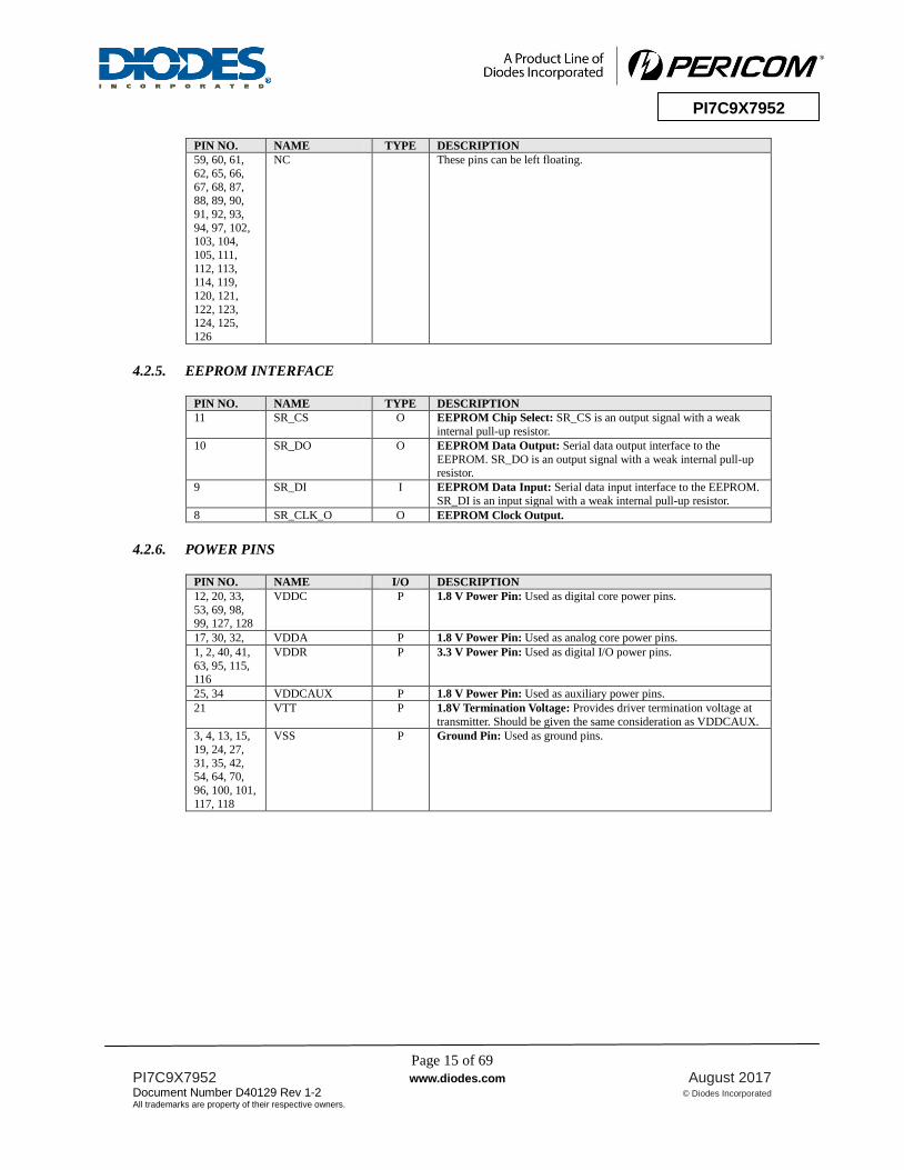
59, 60, 61,
62, 65, 66,
67, 68, 87, 88, 89, 90,
91, 92, 93,
94, 97, 102, 103, 104,
105, 111,
112, 113, 114, 119,
120, 121,
122, 123, 124, 125,
126
NC These pins can be left floating.
4.2.5. EEPROM INTERFACE
PIN NO. NAME TYPE DESCRIPTION
11 SR_CS O EEPROM Chip Select: SR_CS is an output signal with a weak
internal pull-up resistor.
10 SR_DO O EEPROM Data Output: Serial data output interface to the
EEPROM. SR_DO is an output signal with a weak internal pull-up resistor.
9 SR_DI I EEPROM Data Input: Serial data input interface to the EEPROM.
SR_DI is an input signal with a weak internal pull-up resistor.
8 SR_CLK_O O EEPROM Clock Output.
4.2.6. POWER PINS
PIN NO. NAME I/O DESCRIPTION
12, 20, 33,
53, 69, 98, 99, 127, 128
VDDC P 1.8 V Power Pin: Used as digital core power pins.
17, 30, 32, VDDA P 1.8 V Power Pin: Used as analog core power pins.
1, 2, 40, 41,
63, 95, 115, 116
VDDR P 3.3 V Power Pin: Used as digital I/O power pins.
25, 34 VDDCAUX P 1.8 V Power Pin: Used as auxiliary power pins.
21 VTT P 1.8V Termination Voltage: Provides driver termination voltage at
transmitter. Should be given the same consideration as VDDCAUX.
3, 4, 13, 15,
19, 24, 27,
31, 35, 42, 54, 64, 70,
96, 100, 101,
117, 118
VSS P Ground Pin: Used as ground pins.
Page 16 of 69
PI7C9X7952 www.diodes.com August 2017
Document Number D40129 Rev 1-2 © Diodes Incorporated
All trademarks are property of their respective owners.
PI7C9X7952
5. FUNCTIONAL DESCRIPTION
The PI7C9X7952 is an integrated solution of two high-performance 16C550 UARTs with one x1 PCI
Express host interface. The PCI Express host interface is compliant with the PCI Express Base
Specification 1.1, PCI Express CEM Specification 1.1, and PCI Power Management 1.2. In addition, the
chip is compliant with the Advanced Configuration Power Interface (ACPI) Specification and the PCI
Standard Hot-Plug Controller (SHPC) and Subsystem Specification Revision 1.0. The x1 PCI Express host
interface supports up to 2.5 Gbps bandwidth and complete PCI Express configuration register set.
The PCI Express interface allows direct access to the configuration and status registers of the UART
channels.
The UARTs in the PI7C9X7952 support the complete register set of the 16C550-type devices.
The UARTs support Baud Rates up to 15 Mbps in asynchronous mode. Each UART channel has 128-byte
deep transmit and receive FIFOs. The high-speed FIFOs reduce CPU utilization and improve data
throughput. In addition, the UARTs support enhanced features including automated in-band flow control
using programmable Xon/ Xoff in both directions, automated out-band flow control using CTS#/ RTS#
and/or DRS#/ DTR#, and arbitrary transmit and receive trigger levels.
5.1. CONFIGURATION SPACE
The PI7C9X7952 has two sets of registers to allow various configuration and status monitoring functions.
The PCI Express Configuration Space Registers enable the plug-and-play and auto-configuration when the
device is connected to the PCI Express system bus. The UART configuration and internal registers enable
the general UART operation functions, status control and monitoring.
5.1.1. PCI Express Configuration Space
The PI7C9X7952 is recognized as a PCI Express endpoint, which is mapped into the configuration space as
a single logical device. Each endpoint in the system, including the PI7C9X7952, is part of a Hierarchy
Domains originated by the Root Complex, which is a tree with a Root Port at its head in the configuration
space. The device configuration registers are implemented for the user to access the functionalities provided
by the PCI Express specification. The specification utilizes a flat memory-mapped configuration space to
access device configuration registers.
All PCI Express endpoints facilitate a PCI-compatible configuration space to maintain compatibility with
PCI software configuration mechanism. PCI Local Bus Specification, Revision 3.0 allocates 256 bytes per
device function. PCI Express Base Specification 1.1 extends the configuration space to 4096 bytes to allow
enhanced features. The first 256 bytes of the PCI Express Configuration Space are PCI 3.0 compatible
region, and the rest of the 4096 bytes are PCI Express Configuration Space. The user can access the PCI 3.0
compatible region either by conventional PCI 3.0 configuration addresses or by the PCI Express
memory-mapping addresses. These two types of accesses to the PCI 3.0 compatible region have identical
results. The enhanced features in the PCI Express configuration space can only be accessed by PCI Express
memory-mapping accesses.
5.1.2. UART Configuration Space
Through the UART registers, the user can control and monitor various functionalities of the UARTs on the
PI7C9X7952 including FIFOs, interrupt status, line status, modem status and sample clock. Each of the
UART’s transmit and receive data FIFOs can be conveniently accessed by reading and writing the registers
in the UART configuration space. These registers allow flexible programming capability and versatile
Page 17 of 69
PI7C9X7952 www.diodes.com August 2017
Document Number D40129 Rev 1-2 © Diodes Incorporated
All trademarks are property of their respective owners.
PI7C9X7952
device operations of the PI7C9X7952. Each UART is accessed through an 8-byte I/O blocks. The addresses
of the UART blocks are offset by the base address referred by the Base Address Register (BAR). The value
of the base address is loaded from the I/O or Memory Base Address defined in the PCI Express
configuration space.
The PI7C9X7952 also supports enhanced features such as Xon/Xoff, automatic flow control, Baud Rate
prescaling and various status monitoring. These enhanced features are available through the memory
address offset by the BAR in the PCI Express configuration space.
The basic features available in the registers in I/O mode are also available in the registers in
memory-mapping mode. Accesses to these registers are equivalent in these two modes.
The UARTs on the PI7C9X7952 supports operations in 16C450, 16C550 and 16C950 modes. These modes
of operation are selected by writing the SFR, FCR and EFR registers. The PI7C9X7952 is backward
compatible with these modes of operation.
5.2. DEVICE OPERATION
The PI7C9X7952 is configured by the Root Complex in the bootstrap process during system start-up.
The Root Complex performs bus scans and recognizes the device by reading vendor and device IDs. Upon
successful device identification, the system then loads device-specific driver software and allocates I/O,
memory and interrupt resources. The driver software allows the user to access the functions of the device
by reading and writing the UART registers. The PCI Express interface incorporates convenient device
operation and high system performance.
5.2.1. Configuration Access
The PI7C9X7952 accepts type 0 configuration read and write accesses defined in the PCI Express Base1.1
Specification. The first 256 bytes of the PCI Express configuration are compatible with PCI 3.0.
5.2.2. I/O Reads/Writes
The PCI Express interface of the PI7C9X7952 decodes incoming transaction packets. If the address is
within the region assigned by the I/O Base Address Registers, the transaction is recognized as an I/O Read
or Write.
5.2.3. Memory Reads/Writes
Similar to the I/O Read/Write, if the address of the transaction packet is within the memory range, a
Memory Read/Write occurs.
Page 18 of 69
PI7C9X7952 www.diodes.com August 2017
Document Number D40129 Rev 1-2 © Diodes Incorporated
All trademarks are property of their respective owners.
PI7C9X7952
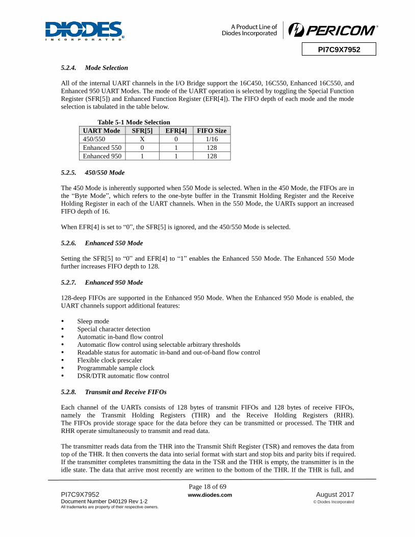
5.2.4. Mode Selection
All of the internal UART channels in the I/O Bridge support the 16C450, 16C550, Enhanced 16C550, and
Enhanced 950 UART Modes. The mode of the UART operation is selected by toggling the Special Function
Register (SFR[5]) and Enhanced Function Register (EFR[4]). The FIFO depth of each mode and the mode
selection is tabulated in the table below.
Table 5-1 Mode Selection
UART Mode SFR[5] EFR[4] FIFO Size
450/550 X 0 1/16
Enhanced 550 0 1 128
Enhanced 950 1 1 128
5.2.5. 450/550 Mode
The 450 Mode is inherently supported when 550 Mode is selected. When in the 450 Mode, the FIFOs are in
the “Byte Mode”, which refers to the one-byte buffer in the Transmit Holding Register and the Receive
Holding Register in each of the UART channels. When in the 550 Mode, the UARTs support an increased
FIFO depth of 16.
When EFR[4] is set to “0”, the SFR[5] is ignored, and the 450/550 Mode is selected.
5.2.6. Enhanced 550 Mode
Setting the SFR[5] to “0” and EFR[4] to “1” enables the Enhanced 550 Mode. The Enhanced 550 Mode
further increases FIFO depth to 128.
5.2.7. Enhanced 950 Mode
128-deep FIFOs are supported in the Enhanced 950 Mode. When the Enhanced 950 Mode is enabled, the
UART channels support additional features:
Sleep mode
Special character detection
Automatic in-band flow control
Automatic flow control using selectable arbitrary thresholds
Readable status for automatic in-band and out-of-band flow control
Flexible clock prescaler
Programmable sample clock
DSR/DTR automatic flow control
5.2.8. Transmit and Receive FIFOs
Each channel of the UARTs consists of 128 bytes of transmit FIFOs and 128 bytes of receive FIFOs,
namely the Transmit Holding Registers (THR) and the Receive Holding Registers (RHR).
The FIFOs provide storage space for the data before they can be transmitted or processed. The THR and
RHR operate simultaneously to transmit and read data.
The transmitter reads data from the THR into the Transmit Shift Register (TSR) and removes the data from
top of the THR. It then converts the data into serial format with start and stop bits and parity bits if required.
If the transmitter completes transmitting the data in the TSR and the THR is empty, the transmitter is in the
idle state. The data that arrive most recently are written to the bottom of the THR. If the THR is full, and
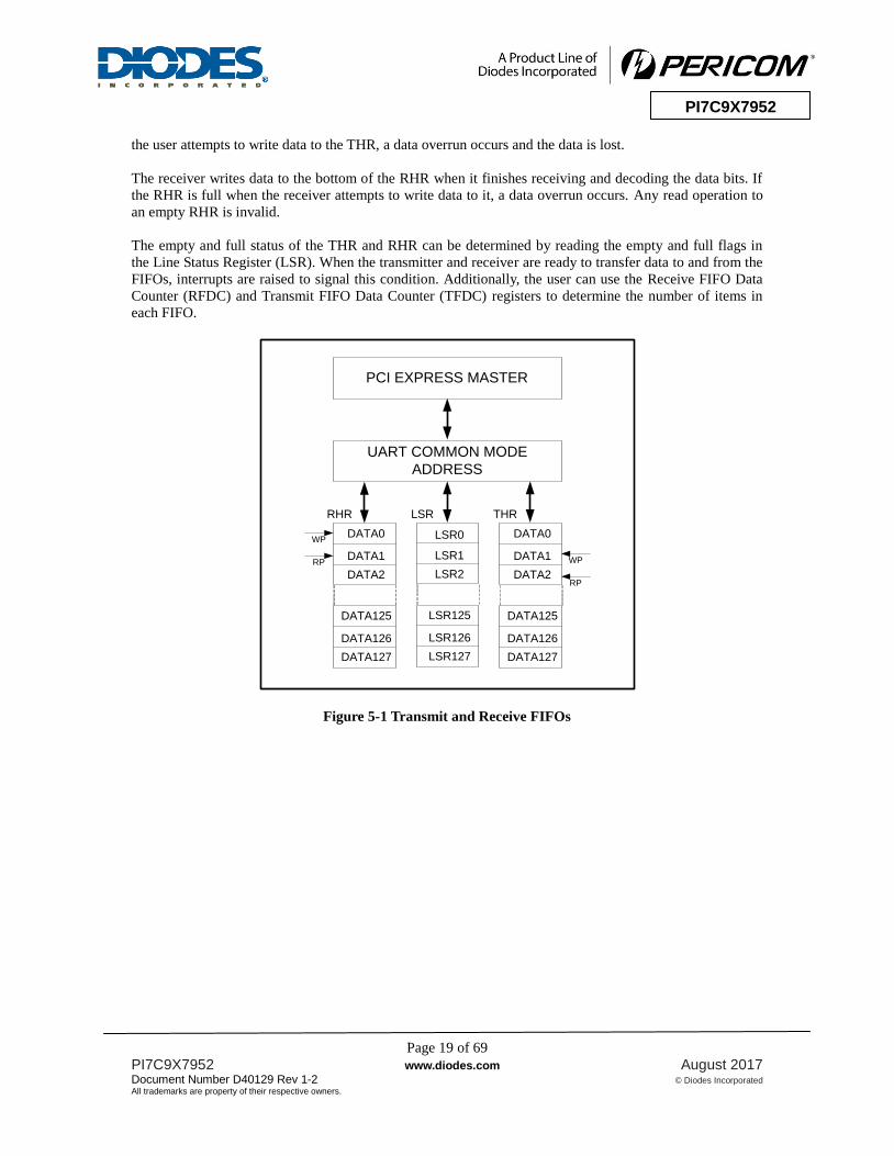
Page 19 of 69
PI7C9X7952 www.diodes.com August 2017
Document Number D40129 Rev 1-2 © Diodes Incorporated
All trademarks are property of their respective owners.
PI7C9X7952
the user attempts to write data to the THR, a data overrun occurs and the data is lost.
The receiver writes data to the bottom of the RHR when it finishes receiving and decoding the data bits. If
the RHR is full when the receiver attempts to write data to it, a data overrun occurs. Any read operation to
an empty RHR is invalid.
The empty and full status of the THR and RHR can be determined by reading the empty and full flags in
the Line Status Register (LSR). When the transmitter and receiver are ready to transfer data to and from the
FIFOs, interrupts are raised to signal this condition. Additionally, the user can use the Receive FIFO Data
Counter (RFDC) and Transmit FIFO Data Counter (TFDC) registers to determine the number of items in
each FIFO.
DATA0
DATA1
DATA2
UART COMMON MODE
ADDRESS
PCI EXPRESS MASTER
RHR LSR THR
DATA125
DATA126
DATA127
LSR0
LSR1
LSR2
LSR125
LSR126
LSR127
DATA0
DATA1
DATA2
DATA125
DATA126
DATA127
RP
WP
RP
WP
Figure 5-1 Transmit and Receive FIFOs
Page 20 of 69
PI7C9X7952 www.diodes.com August 2017
Document Number D40129 Rev 1-2 © Diodes Incorporated
All trademarks are property of their respective owners.
PI7C9X7952
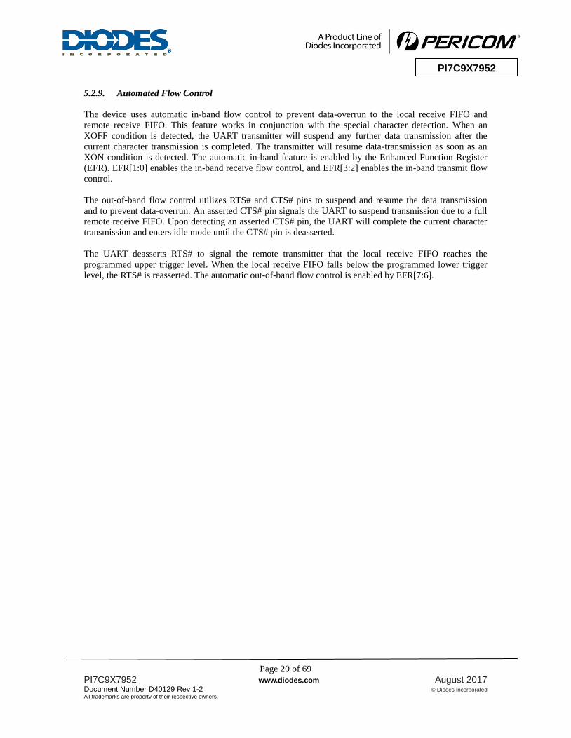
5.2.9. Automated Flow Control
The device uses automatic in-band flow control to prevent data-overrun to the local receive FIFO and
remote receive FIFO. This feature works in conjunction with the special character detection. When an
XOFF condition is detected, the UART transmitter will suspend any further data transmission after the
current character transmission is completed. The transmitter will resume data-transmission as soon as an
XON condition is detected. The automatic in-band feature is enabled by the Enhanced Function Register
(EFR). EFR[1:0] enables the in-band receive flow control, and EFR[3:2] enables the in-band transmit flow
control.
The out-of-band flow control utilizes RTS# and CTS# pins to suspend and resume the data transmission
and to prevent data-overrun. An asserted CTS# pin signals the UART to suspend transmission due to a full
remote receive FIFO. Upon detecting an asserted CTS# pin, the UART will complete the current character
transmission and enters idle mode until the CTS# pin is deasserted.
The UART deasserts RTS# to signal the remote transmitter that the local receive FIFO reaches the
programmed upper trigger level. When the local receive FIFO falls below the programmed lower trigger
level, the RTS# is reasserted. The automatic out-of-band flow control is enabled by EFR[7:6].
Page 21 of 69
PI7C9X7952 www.diodes.com August 2017
Document Number D40129 Rev 1-2 © Diodes Incorporated
All trademarks are property of their respective owners.
PI7C9X7952
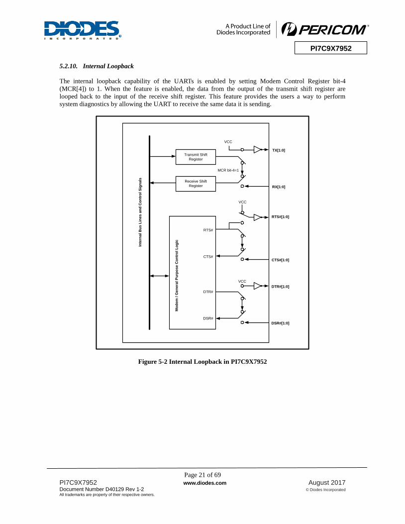
5.2.10. Internal Loopback
The internal loopback capability of the UARTs is enabled by setting Modem Control Register bit-4
(MCR[4]) to 1. When the feature is enabled, the data from the output of the transmit shift register are
looped back to the input of the receive shift register. This feature provides the users a way to perform
system diagnostics by allowing the UART to receive the same data it is sending.
Inte
rnal B
us L
ines a
nd
Co
ntr
ol S
ign
als
Transmit Shift
Register
Receive Shift
Register
VCC
MCR bit-4=1
VCC
VCC
Mo
de
m / G
en
era
l P
urp
ose C
on
tro
l L
og
ic
RTS#
CTS#
DTR#
DSR#
TX[1:0]
RX[1:0]
RTS#[1:0]
CTS#[1:0]
DTR#[1:0]
DSR#[1:0]
Figure 5-2 Internal Loopback in PI7C9X7952

Page 22 of 69
PI7C9X7952 www.diodes.com August 2017
Document Number D40129 Rev 1-2 © Diodes Incorporated
All trademarks are property of their respective owners.
PI7C9X7952
5.2.11. Crystal Oscillator
The PI7C9X7952 uses a crystal oscillator or an external clock source to provide system clock to the Baud
Rate Generator. When a clock source is used, the clock signal should be connected to the XTLI pin, and a
2K pull-up resistor should be connected to the XTLO pin.
When a crystal oscillator is used, the XTLI is the input and XTLO is the output, and the crystal should be
connected in parallel with two capacitors.
R
14.7456 MHz
XTLI XTLO
C1 C2
Figure 5-3 Crystal Oscillator as the Clock Source
XTLI
XTLO
R1
2K
VCC
External Clock
GND
VCC
Figure 5-4 External Clock Source as the Clock Source
Page 23 of 69
PI7C9X7952 www.diodes.com August 2017
Document Number D40129 Rev 1-2 © Diodes Incorporated
All trademarks are property of their respective owners.
PI7C9X7952
escalerDivisor
encyInputFrequBaudRate
Pr*
5.2.12. Baud Rate Generation
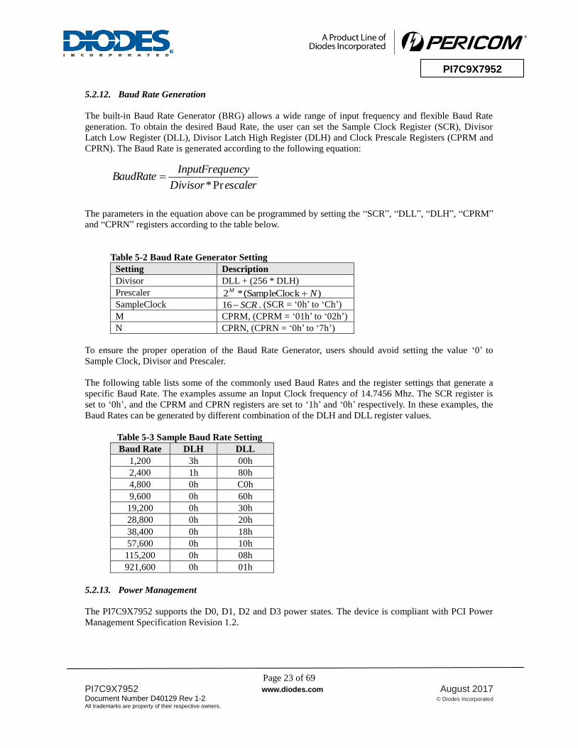
The built-in Baud Rate Generator (BRG) allows a wide range of input frequency and flexible Baud Rate
generation. To obtain the desired Baud Rate, the user can set the Sample Clock Register (SCR), Divisor
Latch Low Register (DLL), Divisor Latch High Register (DLH) and Clock Prescale Registers (CPRM and
CPRN). The Baud Rate is generated according to the following equation:
The parameters in the equation above can be programmed by setting the “SCR”, “DLL”, “DLH”, “CPRM”
and “CPRN” registers according to the table below.
Table 5-2 Baud Rate Generator Setting
Setting Description
Divisor DLL + (256 * DLH)
Prescaler )kSampleCloc(*2 NM
SampleClock SCR16 , (SCR = ‘0h’ to ‘Ch’)
M CPRM, (CPRM = ‘01h’ to ‘02h’)
N CPRN, (CPRN = ‘0h’ to ‘7h’)
To ensure the proper operation of the Baud Rate Generator, users should avoid setting the value ‘0’ to
Sample Clock, Divisor and Prescaler.
The following table lists some of the commonly used Baud Rates and the register settings that generate a
specific Baud Rate. The examples assume an Input Clock frequency of 14.7456 Mhz. The SCR register is
set to ‘0h’, and the CPRM and CPRN registers are set to ‘1h’ and ‘0h’ respectively. In these examples, the
Baud Rates can be generated by different combination of the DLH and DLL register values.
Table 5-3 Sample Baud Rate Setting
Baud Rate DLH DLL
1,200 3h 00h
2,400 1h 80h
4,800 0h C0h
9,600 0h 60h
19,200 0h 30h
28,800 0h 20h
38,400 0h 18h
57,600 0h 10h
115,200 0h 08h
921,600 0h 01h
5.2.13. Power Management
The PI7C9X7952 supports the D0, D1, D2 and D3 power states. The device is compliant with PCI Power
Management Specification Revision 1.2.
Page 24 of 69
PI7C9X7952 www.diodes.com August 2017
Document Number D40129 Rev 1-2 © Diodes Incorporated
All trademarks are property of their respective owners.
PI7C9X7952
6. PCI EXPRESS REGISTER DESCRIPTION
6.1. REGISTER TYPES
REGISTER TYPE DEFINITION
HwInt Hardware Initialization
RO Read Only
WO Write Only
RW Read / Write
RWC Read / Write 1 to Clear
RWCS Sticky - Read Only / Write 1 to Clear
RWS Sticky - Read / Write
6.2. CONFIGURATION REGISTERS
31 – 24 23 – 16 15 – 8 7 – 0 BYTE OFFSET
Device ID Vendor ID 00h
Status Command 04h
Class Code Revision ID 08h
Reserved Header Type Primary Latency
Timer
Cache Line Size 0Ch
Base Address Register 0 10h
Base Address Register 1 14h
Base Address Register 2 18h
Reserved 1Ch~28h
Subsystem ID Subsystem Vendor ID 2Ch
Reserved 30h
Capability Pointer 34h
Reserved 38h
Reserved Interrupt Pin Interrupt Line 3Ch
Power Management Capabilities Next ID = 8C Capability ID = 01 80h
PM Data PPB Support Power Management Data 84h
Message Control Register Next ID =9C Capability ID = 05 8Ch
Message Address Register 90h
Message Upper Address Register 94h
Message Data Register 98h
VPD Register Next ID = A4 Capability ID = 03 9Ch
VPD Data Register A0h
Vendor Define Register(28h) Next ID = E0 Capability ID = 09 A4h
XPIP CSR0 A8h
XPIP CSR1 ACh
ACK Latency Timer Replay Time-out counter B0h
GPIO Data and Control D8h
EEPROM Data EEPROM Control DCh
PCI Express Capability Register Next ID = 00h Capability ID = 10 E0h
Device Capability E4h
Device Status Device Control E8h
Link Capability ECh
Link Status Link Control F0h
Reserved F4h
Reserved F8h
PCI Express Extend Capability Register
Next Capability
Offset = 000h
Capability Version PCI Express Extended Capability
ID = 001h
100h
Uncorrectable Error Status Register 104h
Uncorrectable Error Mask Register 108h
Uncorrectable Error Severity Register 10Ch
Page 25 of 69
PI7C9X7952 www.diodes.com August 2017
Document Number D40129 Rev 1-2 © Diodes Incorporated
All trademarks are property of their respective owners.
PI7C9X7952
31 – 24 23 – 16 15 – 8 7 – 0 BYTE OFFSET
Correctable Error Status Register 110h
Correctable Error Mask Register 114h
Advanced Error Capabilities and Control Register 118h
Header Log Register 11Ch~128h
6.2.1. VENDOR ID REGISTER – OFFSET 00h
BIT FUNCTION TYPE DESCRIPTION
15:0 Vendor ID RO Identifies Pericom as the vendor of this device. The register is
hardwired as 12D8h.
6.2.2. DEVICE ID REGISTER – OFFSET 00h
BIT FUNCTION TYPE DESCRIPTION
31:16 Device ID RO Identifies this device as the PI7C9X7952. Reset to 7952h.
6.2.3. COMMAND REGISTER – OFFSET 04h
BIT FUNCTION TYPE DESCRIPTION
0 I/O Space Enable RW
Controls a device’s response to I/O Space accesses. A value of 0
disables the device response. A value of 1 allows the device to respond to I/O Space accesses.
Reset to 0b.
1 Memory Space
Enable RW
Controls a device’s response to Memory Space accesses. A value of 0
disables the device response. A value of 1 allows the device to
response to memory Space accesses.
Reset to 0b.
2 Bus Master Enable RO It is not implemented. Hardwired to 0b.
3 Special Cycle Enable
RO Does not apply to PCI Express. Must be hardwired to 0b.
4 Memory Write And
Invalidate Enable RO
Does not apply to PCI Express. Must be hardwired to 0b.
5 VGA Palette Snoop Enable
RO Does not apply to PCI Express. Must be hardwired to 0b.
6 Parity Error
Response Enable RW
Controls the device’s response to parity errors. When the bit is set,
the device must take its normal action when a parity error is detected. When the bit is 0, the device sets its Detected Parity Error
Status bit when an error is detected.
Reset to 0b.
7 Wait Cycle Control RO Does not apply to PCI Express. Must be hardwired to 0b.
8 SERR# enable RW
This bit, when set, enables reporting of Non-fatal and Fatal errors
detected by the device to the Root Complex.
Reset to 0b.
9 Fast Back-to-Back
Enable RO
Does not apply to PCI Express. Must be hardwired to 0b.
10 Interrupt Disable RW
Controls the ability of the I/O bridge to generate INTx interrupt
Messages.
Reset to 0b.
15:11 Reserved RO Reset to 00000b.
6.2.4. STATUS REGISTER – OFFSET 04h
BIT FUNCTION TYPE DESCRIPTION
18:16 Reserved RO Reset to 000b.
19 Interrupt Status RO Indicates that an INTx interrupt Message is pending internally to the
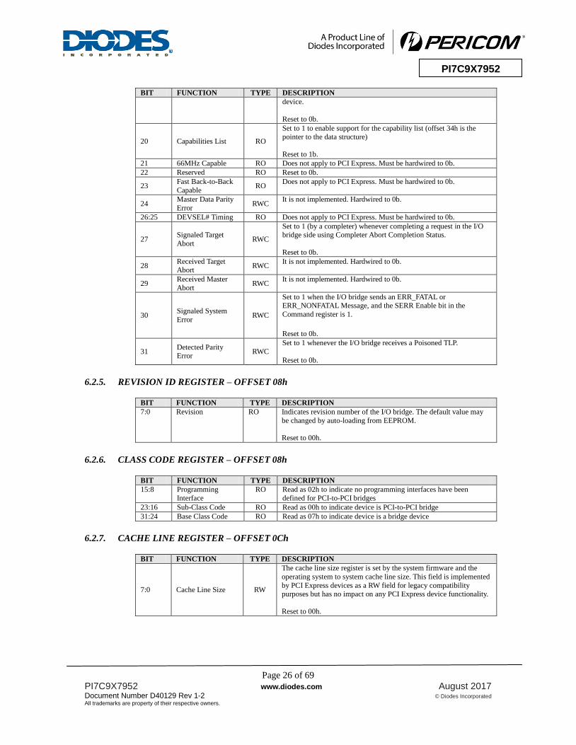
Page 26 of 69
PI7C9X7952 www.diodes.com August 2017
Document Number D40129 Rev 1-2 © Diodes Incorporated
All trademarks are property of their respective owners.
PI7C9X7952
BIT FUNCTION TYPE DESCRIPTION
device.
Reset to 0b.
20 Capabilities List RO
Set to 1 to enable support for the capability list (offset 34h is the pointer to the data structure)
Reset to 1b.
21 66MHz Capable RO Does not apply to PCI Express. Must be hardwired to 0b.
22 Reserved RO Reset to 0b.
23 Fast Back-to-Back
Capable RO
Does not apply to PCI Express. Must be hardwired to 0b.
24 Master Data Parity
Error RWC
It is not implemented. Hardwired to 0b.
26:25 DEVSEL# Timing RO Does not apply to PCI Express. Must be hardwired to 0b.
27 Signaled Target
Abort RWC
Set to 1 (by a completer) whenever completing a request in the I/O bridge side using Completer Abort Completion Status.
Reset to 0b.
28 Received Target Abort
RWC It is not implemented. Hardwired to 0b.
29 Received Master
Abort RWC
It is not implemented. Hardwired to 0b.
30 Signaled System
Error RWC
Set to 1 when the I/O bridge sends an ERR_FATAL or ERR_NONFATAL Message, and the SERR Enable bit in the
Command register is 1.
Reset to 0b.
31 Detected Parity Error
RWC
Set to 1 whenever the I/O bridge receives a Poisoned TLP.
Reset to 0b.
6.2.5. REVISION ID REGISTER – OFFSET 08h
BIT FUNCTION TYPE DESCRIPTION
7:0 Revision RO Indicates revision number of the I/O bridge. The default value may
be changed by auto-loading from EEPROM.
Reset to 00h.
6.2.6. CLASS CODE REGISTER – OFFSET 08h
BIT FUNCTION TYPE DESCRIPTION
15:8 Programming
Interface
RO Read as 02h to indicate no programming interfaces have been
defined for PCI-to-PCI bridges
23:16 Sub-Class Code RO Read as 00h to indicate device is PCI-to-PCI bridge
31:24 Base Class Code RO Read as 07h to indicate device is a bridge device
6.2.7. CACHE LINE REGISTER – OFFSET 0Ch
BIT FUNCTION TYPE DESCRIPTION
7:0 Cache Line Size RW
The cache line size register is set by the system firmware and the
operating system to system cache line size. This field is implemented
by PCI Express devices as a RW field for legacy compatibility purposes but has no impact on any PCI Express device functionality.
Reset to 00h.
Page 27 of 69
PI7C9X7952 www.diodes.com August 2017
Document Number D40129 Rev 1-2 © Diodes Incorporated
All trademarks are property of their respective owners.
PI7C9X7952
6.2.8. MASTER LATENCY TIMER REGISTER – OFFSET 0Ch
BIT FUNCTION TYPE DESCRIPTION
15:8 Latency timer RO Does not apply to PCI Express. Must be hardwired to 00h.
6.2.9. HEADER TYPE REGISTER – OFFSET 0Ch
BIT FUNCTION TYPE DESCRIPTION
23:16 Header Type RO Read as 00h to indicate that the register layout conforms to the standard PCI-to-PCI bridge layout.
6.2.10. BASE ADDRESS REGISTER 0 – OFFSET 10h
BIT FUNCTION TYPE DESCRIPTION
31:0 Base Address 0 RW
Use this I/O base address to map the UART 16550 compatible registers.
The base address can be allocated to 64 Bytes.
Reset to 00000001h.
6.2.11. BASE ADDRESS REGISTER 1 – OFFSET 14h
BIT FUNCTION TYPE DESCRIPTION
31:0 Base Address 1 RW
Use this memory base address to map the UART 16550 compatible
and enhanced registers. The base address can be allocated to 4096 Bytes.
Reset to 00000000h
6.2.12. SUBSYSTEM VENDOR REGISTER – OFFSET 2Ch
BIT FUNCTION TYPE DESCRIPTION
15:0 Sub Vendor ID RO
Indicates the sub-system vendor id. The default value may be
changed by auto-loading from EEPROM.
Reset to 0000h.
6.2.13. SUBSYSTEM ID REGISTER – OFFSET 2Ch
BIT FUNCTION TYPE DESCRIPTION
31:16 Sub System ID RO
Indicates the sub-system device id. The default value may be
changed by auto-loading from EEPROM.
Reset to 0000h.
6.2.14. CAPABILITIES POINTER REGISTER – OFFSET 34h
BIT FUNCTION TYPE DESCRIPTION
7:0 Capabilities Pointer RO
This optional register points to a linked list of new capabilities
implemented by the device. This default value may be changed by auto-loading from EEPROM.
The default value is 80h.
6.2.15. INTERRUPT LINE REGISTER – OFFSET 3Ch
BIT FUNCTION TYPE DESCRIPTION
7:0 Interrupt Line RW Used to communicate interrupt line routing information. POST
Page 28 of 69
PI7C9X7952 www.diodes.com August 2017
Document Number D40129 Rev 1-2 © Diodes Incorporated
All trademarks are property of their respective owners.
PI7C9X7952
BIT FUNCTION TYPE DESCRIPTION
software will write the routing information into this register as it
initializes and configures the system.
Reset to 00h.
6.2.16. INTERRUPT PIN REGISTER – OFFSET 3Ch
BIT FUNCTION TYPE DESCRIPTION
15:8 Interrupt Pin RO Identifies the legacy interrupt Message(s) the device uses.
Reset to 01h.
6.2.17. POWER MANAGEMENT CAPABILITY ID REGISTER – OFFSET 80h
BIT FUNCTION TYPE DESCRIPTION
7:0 Enhanced Capabilities ID
RO Read as 01h to indicate that these are power management enhanced capability registers.
6.2.18. NEXT ITEM POINTER REGISTER – OFFSET 80h
BIT FUNCTION TYPE DESCRIPTION
15:8 Next Item Pointer RO
The pointer points to the Power Management capability register (8Ch).
Reset to 8Ch.
6.2.19. POWER MANAGEMENT CAPABILITIES REGISTER – OFFSET 80h
BIT FUNCTION TYPE DESCRIPTION
18:16 Power Management
Revision RO
Read as 011b to indicate the I/O bridge is compliant to Revision 1.1
of PCI Power Management Interface Specifications.
19 PME# Clock RO Does not apply to PCI Express. Must be hardwired to 0b.
20 Auxiliary Power RO Read as 1b to indicate the I/O bridge forwards the PME# message in
D3cold and an auxiliary power source is required.
21 Device Specific
Initialization RO
Read as 0b to indicate the I/O bridge does not have device specific
initialization requirements. The default value may be changed by auto-loading from EEPROM.
24:22 AUX Current RO Reset as 111b to indicate the I/O bridge need 375 mA in D3 state.
The default value may be changed by auto-loading from EEPROM.
25 D1 Power State
Support RO
Read as 1b to indicate the I/O bridge supports the D1 power management state. The default value may be changed by
auto-loading from EEPROM.
26 D2 Power State
Support RO
Read as 1b to indicate the I/O bridge supports the D2 power management state. The default value may be changed by
auto-loading from EEPROM.
31:27 PME# Support RO
Read as 01000b to indicate the I/O bridge supports the forwarding of
PME# message in all power states. The default value may be changed by auto-loading from EEPROM.
6.2.20. POWER MANAGEMENT DATA REGISTER – OFFSET 84h
BIT FUNCTION TYPE DESCRIPTION
1:0 Power State RW
Indicates the current power state of the I/O bridge. Writing a value of D0 causes a hot reset without asserting PEREST_L when the
previous state was D3.
00b: D0 state
01b: D1 state
10b: D2 state
Page 29 of 69
PI7C9X7952 www.diodes.com August 2017
Document Number D40129 Rev 1-2 © Diodes Incorporated
All trademarks are property of their respective owners.
PI7C9X7952
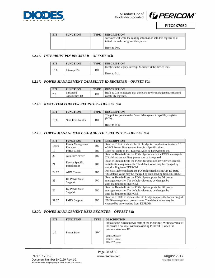
BIT FUNCTION TYPE DESCRIPTION
11b: D3 hot state
Reset to 00b.
2 Reserved RO Read as 0b.
3 No_Soft_Reset RO
When set, this bit indicates that I/O bridge transitioning from D3hot
to D0 does not perform an internal reset.
When clear, an internal reset is performed when power state transits from D3hot to D0. The default value may be changed by
auto-loading from EEPROM.
Reset to 0b.
7:4 Reserved RO Read as 0h.
8 PME# Enable RW
When asserted, the I/O bridge will generate the PME# message.
Reset to 0b.
12:9 Data Select RW
Select data registers.
Reset to 0h.
14:13 Data Scale RO Read as 00b.
15 PME status RO
Indicates that the PME# message is pending internally to the I/O
bridge.
Reset to 0b.
6.2.21. PPB SUPPORT EXTENSIONS – OFFSET 84h
BIT FUNCTION TYPE DESCRIPTION
21:16 Reserved RO Reset to 000000b.
22 B2_B3 Support for
D3HOT RO
Does not apply to PCI Express. Must be hardwired to 0b.
23 Bus Power / Clock
Control Enable RO
Does not apply to PCI Express. Must be hardwired to 0b.
6.2.22. PM DATA REGISTER – OFFSET 84h
BIT FUNCTION TYPE DESCRIPTION
31:24 PM Data Register RO
PM Data Register.
Reset to 00h
6.2.23. MESSAGE SIGNALED INTERRUPTS (MSI) Capability ID Register 8Ch
BIT FUNCTION TYPE DESCRIPTION
7:0 Enhanced
Capability ID RO
Read as 05h to indicate that this is Message Signaled Interrupt
capability register.
6.2.24. MESSAGE SIGNALED INTERRUPTS (MSI) NEXT ITEM POINTER 8Ch
BIT FUNCTION TYPE DESCRIPTION
15:8 Next Item Pointer RO
The pointer points to the Vendor Specific capability register (9Ch).
Reset to 9Ch.
6.2.25. MESSAGE CONTROL REGISTER – OFFSET 8Ch
BIT FUNCTION TYPE DESCRIPTION
16 MSI Enable RW
0b: The function is prohibited from using MSI to request service 1b: The function is permitted to use MSI to request service and is
prohibited from using its INTx # pin

Page 30 of 69
PI7C9X7952 www.diodes.com August 2017
Document Number D40129 Rev 1-2 © Diodes Incorporated
All trademarks are property of their respective owners.
PI7C9X7952
BIT FUNCTION TYPE DESCRIPTION
Reset to 1’b0.
19:17 Multiple Message
Capable RO
Read as 3’b000.
22:20 Multiple Message
Enable RW
Reset to 3’b000.
23 64-bit address capable
RO
0b: The function is not capable of generating a 64-bit message address
1b: The function is capable of generating a 64-bit message address
Reset to 1’b1.
31:24 Reserved RO Reset to 8’h00.
6.2.26. MESSAGE ADDRESS REGISTER – OFFSET 90h
BIT FUNCTION TYPE DESCRIPTION
1:0 Reserved RO Reset to 00b.
31:2 Message Address RW
If the message enable bit is set, the contents of this register specify the DWORD aligned address for MSI memory write transaction.
Reset to 0.
6.2.27. MESSAGE UPPER ADDRESS REGISTER – OFFSET 94h
BIT FUNCTION TYPE DESCRIPTION
31:0 Message Upper Address
RW
This register is only effective if the device supports a 64-bit message
address is set.
Reset to 00000000h.
6.2.28. MESSAGE DATA REGISTER – OFFSET 98h
BIT FUNCTION TYPE DESCRIPTION
15:0 Message Data RW Reset to 0000h.
6.2.29. VPD CAPABILITY ID REGISTER – OFFSET 9Ch
BIT FUNCTION TYPE DESCRIPTION
7:0 Enhanced
Capabilities ID RO
Read as 03h to indicate that these are VPD enhanced capability
registers.
6.2.30. NEXT ITEM POINTER REGISTER – OFFSET 9Ch
BIT FUNCTION TYPE DESCRIPTION
15:8 Next Item Pointer RO
The pointer points to the VPD capability register (A4h).
Reset to A4h
6.2.31. VPD REGISTER – OFFSET 9Ch
BIT FUNCTION TYPE DESCRIPTION
16 VPD Start RW
Starts VPD read or write cycle. Assert by software and is
de-asserted by hardware.
Reset to 0b.
17 VPD Operation RW 0b: Performs VPD read command to VPD table at the location as
specified in VPD address
1b: Performs VPD write command to VPD table at the location
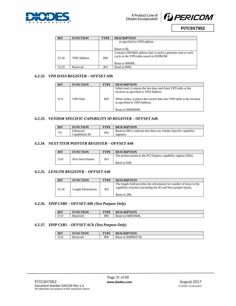
Page 31 of 69
PI7C9X7952 www.diodes.com August 2017
Document Number D40129 Rev 1-2 © Diodes Incorporated
All trademarks are property of their respective owners.
PI7C9X7952
BIT FUNCTION TYPE DESCRIPTION
as specified in VPD address
Reset to 0b.
22:18 VPD Address RW
Contains DWORD address that is used to generate read or write cycle to the VPD table stored in EEPROM.
Reset to 00000b.
31:23 Reserved RO Read as 000h.
6.2.32. VPD DATA REGISTER – OFFSET A0h
BIT FUNCTION TYPE DESCRIPTION
31:0 VPD Data RW
When read, it returns the last data read from VPD table at the location as specified in VPD Address.
When writes, it places the current data into VPD table at the location
as specified in VPD Address.
Reset to 00000000h.
6.2.33. VENDOR SPECIFIC CAPABILITY ID REGISTER – OFFSET A4h
BIT FUNCTION TYPE DESCRIPTION
7:0 Enhanced
Capabilities ID RO
Read as 09h to indicate that these are Vendor Specific capability
registers.
6.2.34. NEXT ITEM POINTER REGISTER – OFFSET A4h
BIT FUNCTION TYPE DESCRIPTION
15:8 Next Item Pointer RO
The pointer points to the PCI Express capability register (E0h).
Reset to E0h.
6.2.35. LENGTH REGISTER – OFFSET A4h
BIT FUNCTION TYPE DESCRIPTION
31:16 Length Information RO
The length field provides the information for number of bytes in the
capability structure (including the ID and Next pointer bytes).
Reset to 28h.
6.2.36. XPIP CSR0 – OFFSET A8h (Test Purpose Only)
BIT FUNCTION TYPE DESCRIPTION
31:0 Reserved RW Reset to 04001060h.
6.2.37. XPIP CSR1 – OFFSET ACh (Test Purpose Only)
BIT FUNCTION TYPE DESCRIPTION
31:0 Reserved RW Reset to 004000271h.
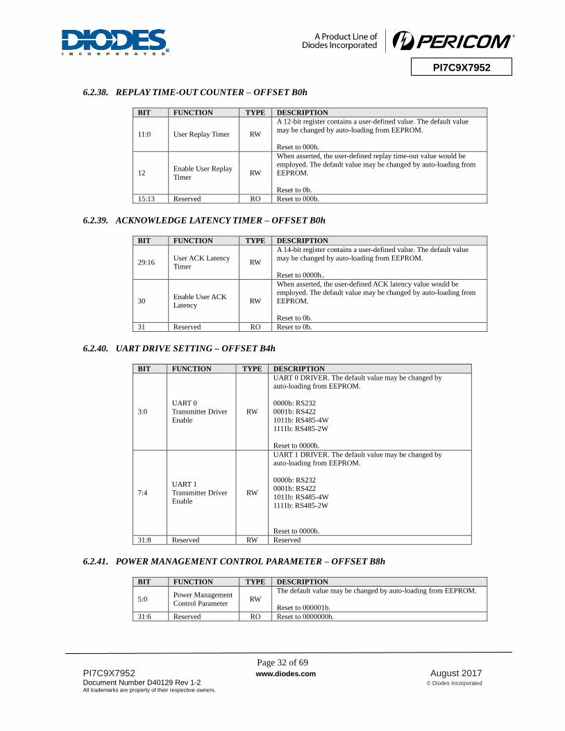
Page 32 of 69
PI7C9X7952 www.diodes.com August 2017
Document Number D40129 Rev 1-2 © Diodes Incorporated
All trademarks are property of their respective owners.
PI7C9X7952
6.2.38. REPLAY TIME-OUT COUNTER – OFFSET B0h
BIT FUNCTION TYPE DESCRIPTION
11:0 User Replay Timer RW
A 12-bit register contains a user-defined value. The default value
may be changed by auto-loading from EEPROM.
Reset to 000h.
12 Enable User Replay
Timer RW
When asserted, the user-defined replay time-out value would be
employed. The default value may be changed by auto-loading from EEPROM.
Reset to 0b.
15:13 Reserved RO Reset to 000b.
6.2.39. ACKNOWLEDGE LATENCY TIMER – OFFSET B0h
BIT FUNCTION TYPE DESCRIPTION
29:16 User ACK Latency Timer
RW
A 14-bit register contains a user-defined value. The default value
may be changed by auto-loading from EEPROM.
Reset to 0000h..
30 Enable User ACK Latency
RW
When asserted, the user-defined ACK latency value would be employed. The default value may be changed by auto-loading from
EEPROM.
Reset to 0b.
31 Reserved RO Reset to 0b.
6.2.40. UART DRIVE SETTING – OFFSET B4h
BIT FUNCTION TYPE DESCRIPTION
3:0
UART 0
Transmitter Driver
Enable
RW
UART 0 DRIVER. The default value may be changed by auto-loading from EEPROM.
0000b: RS232
0001b: RS422
1011b: RS485-4W
1111b: RS485-2W
Reset to 0000b.
7:4
UART 1
Transmitter Driver Enable
RW
UART 1 DRIVER. The default value may be changed by auto-loading from EEPROM.
0000b: RS232 0001b: RS422
1011b: RS485-4W
1111b: RS485-2W
Reset to 0000b.
31:8 Reserved RW Reserved
6.2.41. POWER MANAGEMENT CONTROL PARAMETER – OFFSET B8h
BIT FUNCTION TYPE DESCRIPTION
5:0 Power Management
Control Parameter RW
The default value may be changed by auto-loading from EEPROM.
Reset to 000001b.
31:6 Reserved RO Reset to 0000000h.

Page 33 of 69
PI7C9X7952 www.diodes.com August 2017
Document Number D40129 Rev 1-2 © Diodes Incorporated
All trademarks are property of their respective owners.
PI7C9X7952
6.2.42. DEBUG REGISTER 1 – OFFSET BCh (Test Purpose Only)
BIT FUNCTION TYPE DESCRIPTION
31:0 Debug Register 1 RO
Used for test purpose only.
Reset to 00000000h.
6.2.43. DEBUG REGISTER 2 – OFFSET C0h (Test Purpose Only)
BIT FUNCTION TYPE DESCRIPTION
31:0 Debug Register 2 RO
Used for test purpose only.
Reset to 00000000h.
6.2.44. DEBUG REGISTER 3 – OFFSET C4h (Test Purpose Only)
BIT FUNCTION TYPE DESCRIPTION
31:0 Debug Register 3 RO Used for test purpose only.
Reset to 00000000h.
6.2.45. DEBUG REGISTER 4 – OFFSET C8h (Test Purpose Only)
BIT FUNCTION TYPE DESCRIPTION
0 Low Driver Current HwInt It indicates the status of the strapping pin LODRV. The default value may be changed by auto-loading from EEPROM.
1 High Driver Current HwInt It indicates the status of the strapping pin HIDRV. The default value
may be changed by auto-loading from EEPROM.
5:2 Driver Transmit Current
HwInt It indicates the status of the strapping pins DTX[3:0]. The default value may be changed by auto-loading from EEPROM.
9:6
De-emphasis
Transmit Equalization
HwInt
It indicates the status of the strapping pins DEQ[3:0]. The default
value may be changed by auto-loading from EEPROM.
11:10
Receive
Termination
Adjustment
HwInt
It indicates the status of the strapping pins RXTRMADJ[1:0]. The
default value may be changed by auto-loading from EEPROM.
13:12
Transmit
Termination
Adjustment
HwInt
It indicates the status of the strapping pins TXTRMADJ[1:0]. The
default value may be changed by auto-loading from EEPROM.
31:14 Reserved RO Reset to 00000h.
6.2.46. GPIO CONTROL REGISTER – OFFSET D8h
BIT FUNCTION TYPE DESCRIPTION
7:0 GPIO Input RO
The current state of the GPIO[x] pin can be read from bit[x] in this
register, where x=7 to 0. The bits are effective only when the corresponding GPIO I/O Enable bits are set to “0”.
15:8 GPIO I/O Enable RW
These 8 bits determine whether the GPIO pins are input or output
pins. Bit[x+8] corresponds to GPIO[x], where x=7 to 0. If the bit is set to “0”, the corresponding GPIO pin is an input pin. If the bit is set
to “1”, the corresponding GPIO pin is an output pin.
23:16 GPIO Output RW
The current state of the GPIO[x] pin can be written by bit[x+16] in
this register, where x=7 to 0. The bits are effective only when the corresponding GPIO I/O Enable bits are set to “1”.
31:24 Reserved RO Reserved
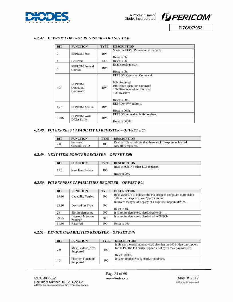
Page 34 of 69
PI7C9X7952 www.diodes.com August 2017
Document Number D40129 Rev 1-2 © Diodes Incorporated
All trademarks are property of their respective owners.
PI7C9X7952
6.2.47. EEPROM CONTROL REGISTER – OFFSET DCh
BIT FUNCTION TYPE DESCRIPTION
0 EEPROM Start RW
Starts the EEPROM read or write cycle.
Reset to 0b.
1 Reserved RO Reset to 0b.
2 EEPROM Preload Control
RW
Enable preload start.
Reset to 0b.
4:3
EEPROM
Operation Command
RW
EEPROM Operation Command.
00b: Reserved 01b: Write operation command
10b: Read operation command
11b: Reserved
Reset to 00b.
15:5 EEPROM Address RW EEPROM RW address.
Reset to 000h.
31:16 EEPROM Write
DATA Buffer RW
EEPROM write data buffer register.
Reset to 0000h.
6.2.48. PCI EXPRESS CAPABILITY ID REGISTER – OFFSET E0h
BIT FUNCTION TYPE DESCRIPTION
7:0 Enhanced Capabilities ID
RO Read as 10h to indicate that these are PCI express enhanced capability registers.
6.2.49. NEXT ITEM POINTER REGISTER – OFFSET E0h
BIT FUNCTION TYPE DESCRIPTION
15:8 Next Item Pointer RO
Read as 00h. No other ECP registers.
Reset to 00h.
6.2.50. PCI EXPRESS CAPABILITIES REGISTER – OFFSET E0h
BIT FUNCTION TYPE DESCRIPTION
19:16 Capability Version RO Read as 0001b to indicate the I/O bridge is compliant to Revision 1.0a of PCI Express Base Specifications.
23:20 Device/Port Type RO
Indicates the type of Legacy PCI Express Endpoint device.
Reset to 1h.
24 Slot Implemented RO It is not implemented. Hardwired to 0b.
29:25 Interrupt Message
Number RO
It is not implemented. Hardwired to 00000b.
31:30 Reserved RO Reset to 00b.
6.2.51. DEVICE CAPABILITIES REGISTER – OFFSET E4h
BIT FUNCTION TYPE DESCRIPTION
2:0 Max_Payload_Size Supported
RO
Indicates the maximum payload size that the I/O bridge can support
for TLPs. The I/O bridge supports 128 bytes max payload size.
Reset to000b.
4:3 Phantom Functions
Supported RO
It is not implemented. Hardwired to 00b.

Page 35 of 69
PI7C9X7952 www.diodes.com August 2017
Document Number D40129 Rev 1-2 © Diodes Incorporated
All trademarks are property of their respective owners.
PI7C9X7952
BIT FUNCTION TYPE DESCRIPTION
5 Extended Tag Field
Supported RO
It is not implemented. Hardwired to 0b.
8:6 Endpoint L0s Acceptable Latency
RO
Acceptable total latency that an Endpoint can withstand due to the
transition from L0s state to the L0 state.
Reset to 000b.
11:9 Endpoint L1
Acceptable Latency RO
Acceptable total latency that an Endpoint can withstand due to the transition from L1 state to the L0 state.
Reset to 000b.
12 Attention Button
Present RO
It is not implemented. Hardwired to 0b.
13 Attention Indicator
Present RO
It is not implemented. Hardwired to 0b.
14 Power Indicator
Present RO
It is not implemented. Hardwired to 0b.
15 Role_Base Error
Reporting RO
When set, indicated that the device implements the functionality
originally defined in the Error Reporting ECN. The default value may be changed by auto-loading from EEPROM.
Reset to 1b.
17:16 Reserved RO Reset to 00b.
25:18 Captured Slot Power
Limit Value RO
In combination with the Slot Power Limit Scale value, specifies the
upper limit on power supplied by slot.
This value is set by the Set_Slot_Power_Limit message or
hardwired to “00h”.
Reset to 00b.
27:26 Captured Slot Power
Limit Scale RO
Specifies the scale used for the Slot Power Limit Value.
This value is set by the Set_Slot_Power_Limit message or
hardwired to “00b”.
Reset to 00b.
31:28 Reserved RO Reset to 0h.
6.2.52. DEVICE CONTROL REGISTER – OFFSET E8h
BIT FUNCTION TYPE DESCRIPTION
0 Correctable Error
Reporting Enable RW
0b: Disable Correctable Error Reporting. 1b: Enable Correctable Error Reporting.
Reset to 0b.
1 Non-Fatal Error
Reporting Enable RW
0b: Disable Non-Fatal Error Reporting.
1b: Enable Non-Fatal Error Reporting.
Reset to 0b.
2 Fatal Error
Reporting Enable RW
0b: Disable Fatal Error Reporting.
1b: Enable Fatal Error Reporting.
Reset to 0b.
3
Unsupported
Request Reporting
Enable
RW
0b: Disable Unsupported Request Reporting.
1b: Enable Unsupported Request Reporting.
Reset to 0b.
4 Enable Relaxed
Ordering RO
It is not implemented.
Reset to 0b.
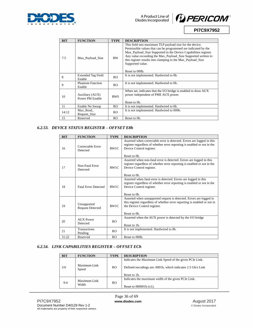
Page 36 of 69
PI7C9X7952 www.diodes.com August 2017
Document Number D40129 Rev 1-2 © Diodes Incorporated
All trademarks are property of their respective owners.
PI7C9X7952
BIT FUNCTION TYPE DESCRIPTION
7:5 Max_Payload_Size RW
This field sets maximum TLP payload size for the device.
Permissible values that can be programmed are indicated by the
Max_Payload_Size Supported in the Device Capabilities register. Any value exceeding the Max_Payload_Size Supported written to
this register results into clamping to the Max_Payload_Size
Supported value.
Reset to 000b.
8 Extended Tag Field Enable
RO It is not implemented. Hardwired to 0b.
9 Phantom Function
Enable RO
It is not implemented. Hardwired to 0b.
10 Auxiliary (AUX)
Power PM Enable RWS
When set, indicates that the I/O bridge is enabled to draw AUX power independent of PME AUX power.
Reset to 0b.
11 Enable No Snoop RO It is not implemented. Hardwired to 0b.
14:12 Max_Read_
Request_Size RO
It is not implemented. Hardwired to 000b.
15 Reserved RO Reset to 0b.
6.2.53. DEVICE STATUS REGISTER – OFFSET E8h
BIT FUNCTION TYPE DESCRIPTION
16 Correctable Error
Detected RW1C
Asserted when correctable error is detected. Errors are logged in this
register regardless of whether error reporting is enabled or not in the
Device Control register.
Reset to 0b.
17 Non-Fatal Error
Detected RW1C
Asserted when non-fatal error is detected. Errors are logged in this
register regardless of whether error reporting is enabled or not in the Device Control register.
Reset to 0b.
18 Fatal Error Detected RW1C
Asserted when fatal error is detected. Errors are logged in this
register regardless of whether error reporting is enabled or not in the
Device Control register.
Reset to 0b.
19 Unsupported Request Detected
RW1C
Asserted when unsupported request is detected. Errors are logged in this register regardless of whether error reporting is enabled or not in
the Device Control register.
Reset to 0b.
20 AUX Power Detected
RO
Asserted when the AUX power is detected by the I/O bridge
Reset to 1b.
21 Transactions
Pending RO
It is not implemented. Hardwired to 0b.
31:22 Reserved RO Reset to 000h.
6.2.54. LINK CAPABILITIES REGISTER – OFFSET ECh
BIT FUNCTION TYPE DESCRIPTION
3:0 Maximum Link
Speed RO
Indicates the Maximum Link Speed of the given PCIe Link.
Defined encodings are: 0001b, which indicates 2.5 Gb/s Link
Reset to 1h.
9:4 Maximum Link
Width RO
Indicates the maximum width of the given PCIe Link.
Reset to 000001b (x1).
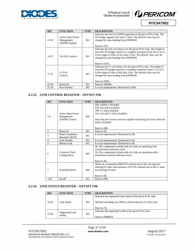
Page 37 of 69
PI7C9X7952 www.diodes.com August 2017
Document Number D40129 Rev 1-2 © Diodes Incorporated
All trademarks are property of their respective owners.
PI7C9X7952
BIT FUNCTION TYPE DESCRIPTION
11:10
Active State Power
Management (ASPM) Support
RO
Indicates the level of ASPM supported on the given PCIe Link. The
I/O bridge supports L0s and L1 entry. The default value may be
changed by auto-loading from EEPROM.
Reset to 11b.
14:12 L0s Exit Latency RO
Indicates the L0s exit latency for the given PCIe Link. The length of
time this I/O bridge requires to complete transition from L0s to L0 is in the range of 256ns to less than 512ns. The default value may be
changed by auto-loading from EEPROM.
Reset to 011b.
17:15 L1 Exit
Latency RO
Indicates the L1 exit latency for the given PCIe Link. The length of
time this I/O bridge requires to complete transition from L1 to L0 is in the range of 16us to less than 32us. The default value may be
changed by auto-loading from EEPROM.
Reset to 000b.
23:18 Reserved RO Reset to 00000b.
31:24 Port Number RO It is not implemented. Hardwired to 00h.
6.2.55. LINK CONTROL REGISTER – OFFSET F0h
BIT FUNCTION TYPE DESCRIPTION
1:0
Active State Power
Management
(ASPM) Control
RW
00b: ASPM is Disabled.
01b: L0s Entry Enabled.
10b: L1 Entry Enabled. 11b: L0s and L1 Entry Enabled.
Note that the receiver must be capable of entering L0s even when the field is disabled.
Reset to 00b.
2 Reserved RO Reset to 0h.
3 Read Completion
Boundary (RCB) RO
It is not implemented. Hardwired to 0b.
4 Link Disable RO It is not implemented. Hardwired to 0b.
5 Retrain Link RO It is not implemented. Hardwired to 0b.
6 Common Clock Configuration
RW
0b: The components at both ends of a link are operating with
asynchronous reference clock.
1b: The components at both ends of a link are operating with a distributed common reference clock.
Reset to 0b.
7 Extended Synch RW
When set, it transmits 4096 FTS ordered sets in the L0s state for entering L0 state and transmits 1024 TS1 ordered sets in the L1 state
for entering L0 state
Reset to 0b.
15:8 RsvdP RO Reset to 00h.
6.2.56. LINK STATUS REGISTER – OFFSET F0h
BIT FUNCTION TYPE DESCRIPTION
19:16 Link Speed RO
Indicates the negotiated Link Speed of the given PCIe Link.
Defined encodings are: 0001b, which indicates 2.5 Gb/s Link
Reset to 1h.
25:20 Negotiated Link
Width RO
Indicates the negotiated width of the given PCIe Link,
Reset to 000001b.
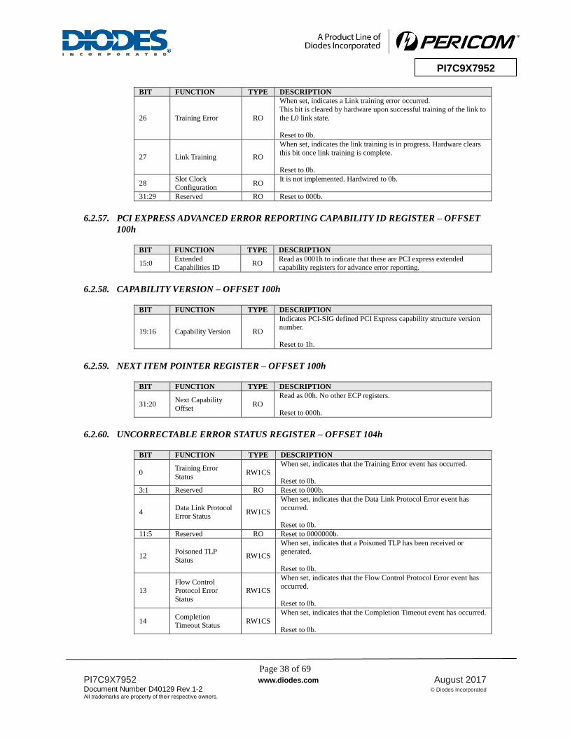
Page 38 of 69
PI7C9X7952 www.diodes.com August 2017
Document Number D40129 Rev 1-2 © Diodes Incorporated
All trademarks are property of their respective owners.
PI7C9X7952
BIT FUNCTION TYPE DESCRIPTION
26 Training Error RO
When set, indicates a Link training error occurred.
This bit is cleared by hardware upon successful training of the link to
the L0 link state.
Reset to 0b.
27 Link Training RO
When set, indicates the link training is in progress. Hardware clears
this bit once link training is complete.
Reset to 0b.
28 Slot Clock Configuration
RO It is not implemented. Hardwired to 0b.
31:29 Reserved RO Reset to 000b.
6.2.57. PCI EXPRESS ADVANCED ERROR REPORTING CAPABILITY ID REGISTER – OFFSET
100h
BIT FUNCTION TYPE DESCRIPTION
15:0 Extended Capabilities ID
RO Read as 0001h to indicate that these are PCI express extended capability registers for advance error reporting.
6.2.58. CAPABILITY VERSION – OFFSET 100h
BIT FUNCTION TYPE DESCRIPTION
19:16 Capability Version RO
Indicates PCI-SIG defined PCI Express capability structure version number.
Reset to 1h.
6.2.59. NEXT ITEM POINTER REGISTER – OFFSET 100h
BIT FUNCTION TYPE DESCRIPTION
31:20 Next Capability Offset
RO
Read as 00h. No other ECP registers.
Reset to 000h.
6.2.60. UNCORRECTABLE ERROR STATUS REGISTER – OFFSET 104h
BIT FUNCTION TYPE DESCRIPTION
0 Training Error
Status RW1CS
When set, indicates that the Training Error event has occurred.
Reset to 0b.
3:1 Reserved RO Reset to 000b.
4 Data Link Protocol Error Status
RW1CS
When set, indicates that the Data Link Protocol Error event has
occurred.
Reset to 0b.
11:5 Reserved RO Reset to 0000000b.
12 Poisoned TLP
Status RW1CS
When set, indicates that a Poisoned TLP has been received or generated.
Reset to 0b.
13 Flow Control Protocol Error
Status
RW1CS
When set, indicates that the Flow Control Protocol Error event has
occurred.
Reset to 0b.
14 Completion Timeout Status
RW1CS
When set, indicates that the Completion Timeout event has occurred.
Reset to 0b.

Page 39 of 69
PI7C9X7952 www.diodes.com August 2017
Document Number D40129 Rev 1-2 © Diodes Incorporated
All trademarks are property of their respective owners.
PI7C9X7952
BIT FUNCTION TYPE DESCRIPTION
15 Completer Abort Status
RW1CS
When set, indicates that the Completer Abort event has occurred.
Reset to 0b.
16 Unexpected
Completion Status RW1CS
When set, indicates that the Unexpected Completion event has occurred.
Reset to 0b.
17 Receiver Overflow Status
RW1CS
When set, indicates that the Receiver Overflow event has occurred.
Reset to 0b.
18 Malformed TLP Status
RW1CS
When set, indicates that a Malformed TLP has been received.
Reset to 0b.
19 ECRC Error Status RW1CS When set, indicates that an ECRC Error has been detected.
Reset to 0b.
20
Unsupported
Request Error
Status
RW1CS
When set, indicates that an Unsupported Request event has occurred.
Reset to 0b.
31:21 Reserved RO Reset to 000h.
6.2.61. UNCORRECTABLE ERROR MASK REGISTER – OFFSET 108h
BIT FUNCTION TYPE DESCRIPTION
0 Training Error
Mask RWS
When set, the Training Error event is not logged in the Header Log
register and not issued as an Error Message to RC either.
Reset to 0b.
3:1 Reserved RO Reset to 000b.
4 Data Link Protocol Error Mask
RWS
When set, the Data Link Protocol Error event is not logged in the
Header Log register and not issued as an Error Message to RC either.
Reset to 0b.
11:5 Reserved RO Reset to 0000000b.
12 Poisoned TLP Mask RWS
When set, an event of Poisoned TLP has been received or generated
is not logged in the Header Log register and not issued as an Error
Message to RC either.
Reset to 0b.
13
Flow Control
Protocol Error
Mask
RWS
When set, the Flow Control Protocol Error event is not logged in the
Header Log register and not issued as an Error Message to RC either.
Reset to 0b.
14 Completion Timeout Mask
RWS
When set, the Completion Timeout event is not logged in the Header
Log register and not issued as an Error Message to RC either.
Reset to 0b.
15 Completer Abort
Mask RWS
When set, the Completer Abort event is not logged in the Header Log register and not issued as an Error Message to RC either.
Reset to 0b.
16 Unexpected
Completion Mask RWS
When set, the Unexpected Completion event is not logged in the Header Log register and not issued as an Error Message to RC either.
Reset to 0b.
17 Receiver Overflow
Mask RWS
When set, the Receiver Overflow event is not logged in the Header
Log register and not issued as an Error Message to RC either.
Reset to 0b.
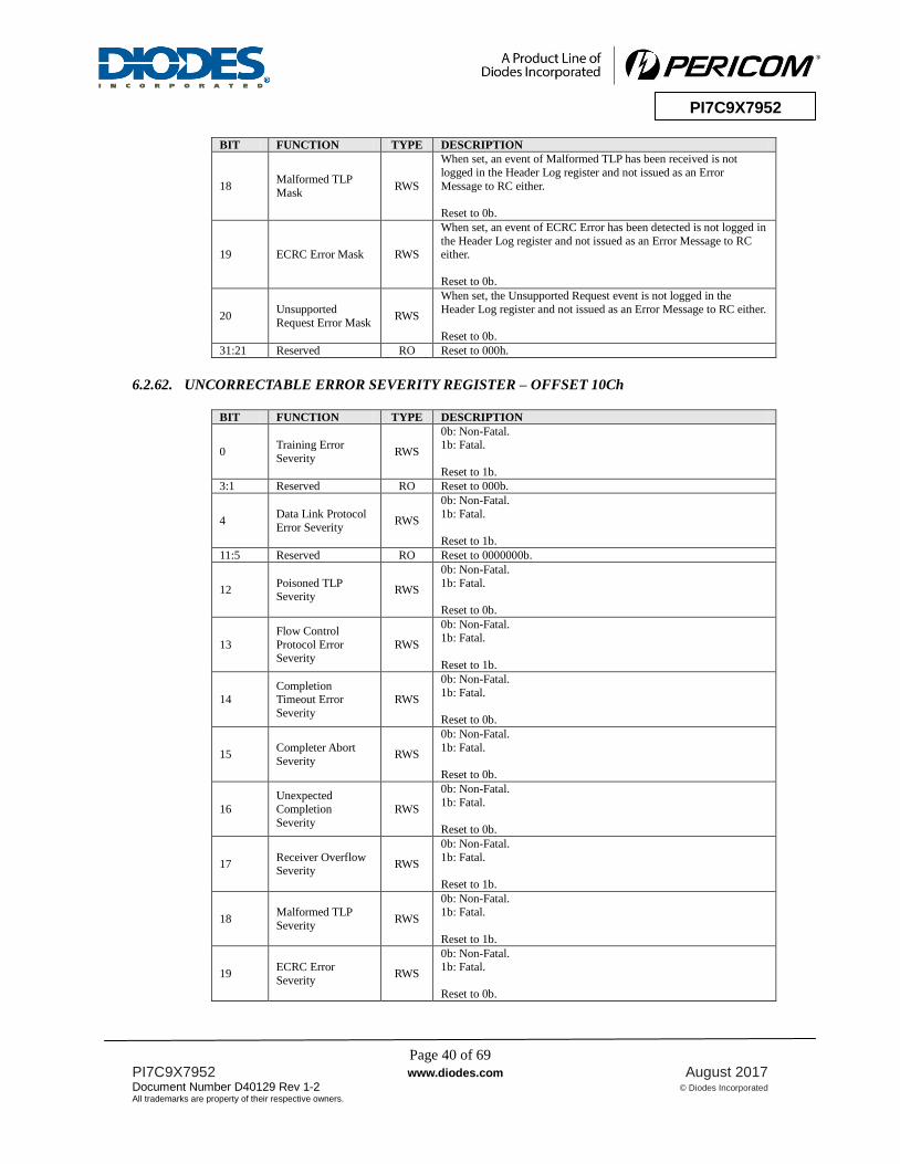
Page 40 of 69
PI7C9X7952 www.diodes.com August 2017
Document Number D40129 Rev 1-2 © Diodes Incorporated
All trademarks are property of their respective owners.
PI7C9X7952
BIT FUNCTION TYPE DESCRIPTION
18 Malformed TLP
Mask RWS
When set, an event of Malformed TLP has been received is not
logged in the Header Log register and not issued as an Error
Message to RC either.
Reset to 0b.
19 ECRC Error Mask RWS
When set, an event of ECRC Error has been detected is not logged in
the Header Log register and not issued as an Error Message to RC either.
Reset to 0b.
20 Unsupported
Request Error Mask RWS
When set, the Unsupported Request event is not logged in the
Header Log register and not issued as an Error Message to RC either.
Reset to 0b.
31:21 Reserved RO Reset to 000h.
6.2.62. UNCORRECTABLE ERROR SEVERITY REGISTER – OFFSET 10Ch
BIT FUNCTION TYPE DESCRIPTION
0 Training Error
Severity RWS
0b: Non-Fatal. 1b: Fatal.
Reset to 1b.
3:1 Reserved RO Reset to 000b.
4 Data Link Protocol
Error Severity RWS
0b: Non-Fatal.
1b: Fatal.
Reset to 1b.
11:5 Reserved RO Reset to 0000000b.
12 Poisoned TLP Severity
RWS
0b: Non-Fatal.
1b: Fatal.
Reset to 0b.
13
Flow Control
Protocol Error
Severity
RWS
0b: Non-Fatal. 1b: Fatal.
Reset to 1b.
14 Completion Timeout Error
Severity
RWS
0b: Non-Fatal.
1b: Fatal.
Reset to 0b.
15 Completer Abort
Severity RWS
0b: Non-Fatal.
1b: Fatal.
Reset to 0b.
16
Unexpected
Completion
Severity
RWS
0b: Non-Fatal.
1b: Fatal.
Reset to 0b.
17 Receiver Overflow Severity
RWS
0b: Non-Fatal.
1b: Fatal.
Reset to 1b.
18 Malformed TLP
Severity RWS
0b: Non-Fatal.
1b: Fatal.
Reset to 1b.
19 ECRC Error
Severity RWS
0b: Non-Fatal. 1b: Fatal.
Reset to 0b.
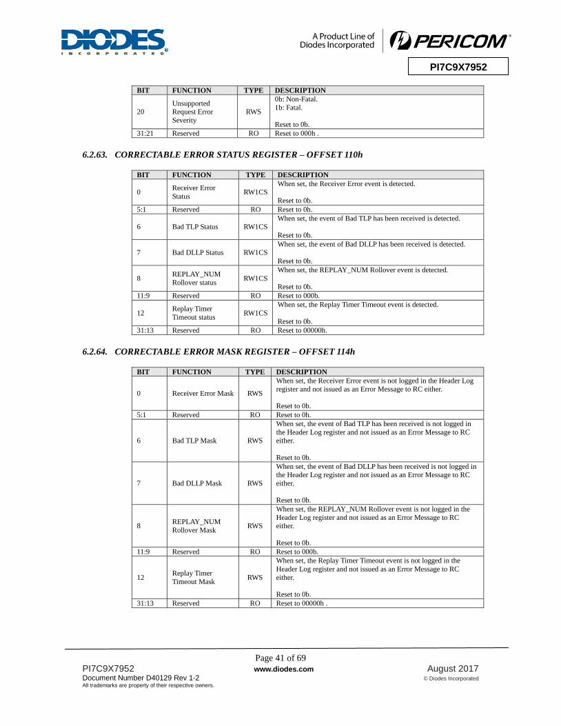
Page 41 of 69
PI7C9X7952 www.diodes.com August 2017
Document Number D40129 Rev 1-2 © Diodes Incorporated
All trademarks are property of their respective owners.
PI7C9X7952
BIT FUNCTION TYPE DESCRIPTION
20 Unsupported Request Error
Severity
RWS
0b: Non-Fatal.
1b: Fatal.
Reset to 0b.
31:21 Reserved RO Reset to 000h .
6.2.63. CORRECTABLE ERROR STATUS REGISTER – OFFSET 110h
BIT FUNCTION TYPE DESCRIPTION
0 Receiver Error
Status RW1CS
When set, the Receiver Error event is detected.
Reset to 0b.
5:1 Reserved RO Reset to 0h.
6 Bad TLP Status RW1CS When set, the event of Bad TLP has been received is detected.
Reset to 0b.
7 Bad DLLP Status RW1CS When set, the event of Bad DLLP has been received is detected.
Reset to 0b.
8 REPLAY_NUM
Rollover status RW1CS
When set, the REPLAY_NUM Rollover event is detected.
Reset to 0b.
11:9 Reserved RO Reset to 000b.
12 Replay Timer
Timeout status RW1CS
When set, the Replay Timer Timeout event is detected.
Reset to 0b.
31:13 Reserved RO Reset to 00000h.
6.2.64. CORRECTABLE ERROR MASK REGISTER – OFFSET 114h
BIT FUNCTION TYPE DESCRIPTION
0 Receiver Error Mask RWS
When set, the Receiver Error event is not logged in the Header Log register and not issued as an Error Message to RC either.
Reset to 0b.
5:1 Reserved RO Reset to 0h.
6 Bad TLP Mask RWS
When set, the event of Bad TLP has been received is not logged in
the Header Log register and not issued as an Error Message to RC either.
Reset to 0b.
7 Bad DLLP Mask RWS
When set, the event of Bad DLLP has been received is not logged in the Header Log register and not issued as an Error Message to RC
either.
Reset to 0b.
8 REPLAY_NUM
Rollover Mask RWS
When set, the REPLAY_NUM Rollover event is not logged in the
Header Log register and not issued as an Error Message to RC either.
Reset to 0b.
11:9 Reserved RO Reset to 000b.
12 Replay Timer
Timeout Mask RWS
When set, the Replay Timer Timeout event is not logged in the
Header Log register and not issued as an Error Message to RC
either.
Reset to 0b.
31:13 Reserved RO Reset to 00000h .
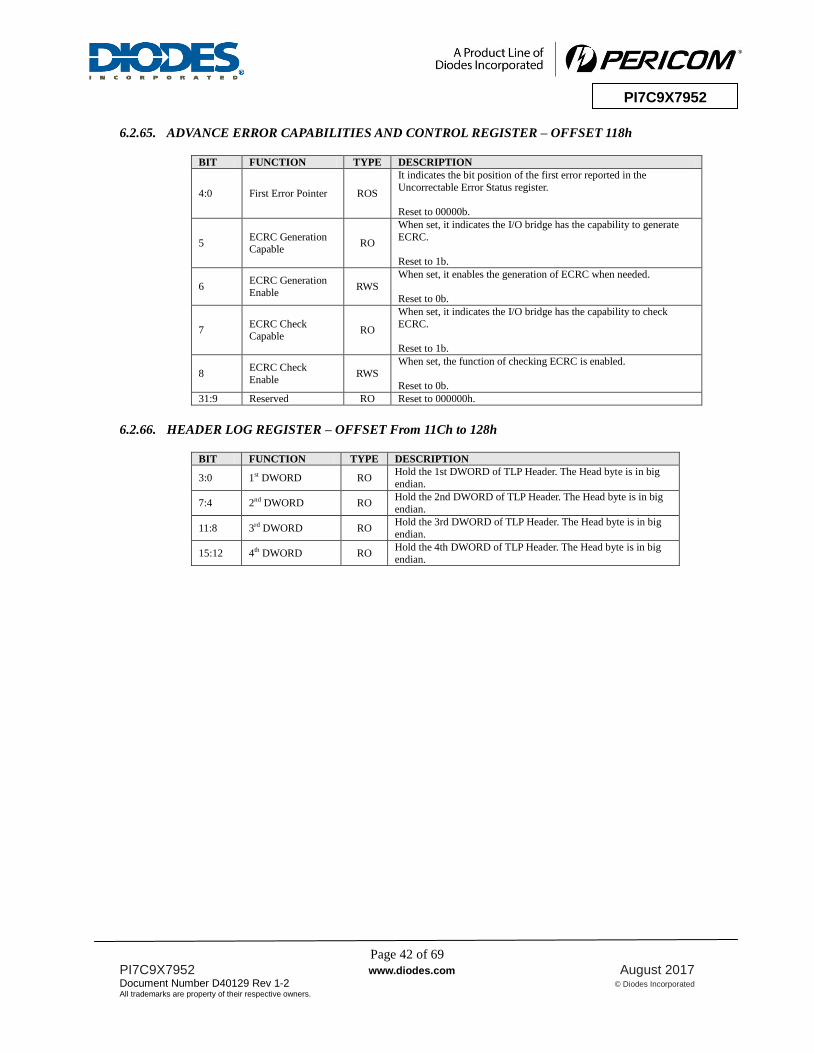
Page 42 of 69
PI7C9X7952 www.diodes.com August 2017
Document Number D40129 Rev 1-2 © Diodes Incorporated
All trademarks are property of their respective owners.
PI7C9X7952
6.2.65. ADVANCE ERROR CAPABILITIES AND CONTROL REGISTER – OFFSET 118h
BIT FUNCTION TYPE DESCRIPTION
4:0 First Error Pointer ROS
It indicates the bit position of the first error reported in the
Uncorrectable Error Status register.
Reset to 00000b.
5 ECRC Generation Capable
RO
When set, it indicates the I/O bridge has the capability to generate
ECRC.
Reset to 1b.
6 ECRC Generation
Enable RWS
When set, it enables the generation of ECRC when needed.
Reset to 0b.
7 ECRC Check Capable
RO
When set, it indicates the I/O bridge has the capability to check
ECRC.
Reset to 1b.
8 ECRC Check
Enable RWS
When set, the function of checking ECRC is enabled.
Reset to 0b.
31:9 Reserved RO Reset to 000000h.
6.2.66. HEADER LOG REGISTER – OFFSET From 11Ch to 128h
BIT FUNCTION TYPE DESCRIPTION
3:0 1st DWORD RO Hold the 1st DWORD of TLP Header. The Head byte is in big
endian.
7:4 2nd DWORD RO Hold the 2nd DWORD of TLP Header. The Head byte is in big
endian.
11:8 3rd DWORD RO Hold the 3rd DWORD of TLP Header. The Head byte is in big
endian.
15:12 4th DWORD RO Hold the 4th DWORD of TLP Header. The Head byte is in big
endian.
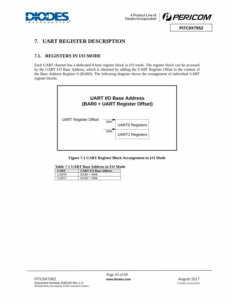
Page 43 of 69
PI7C9X7952 www.diodes.com August 2017
Document Number D40129 Rev 1-2 © Diodes Incorporated
All trademarks are property of their respective owners.
PI7C9X7952
7. UART REGISTER DESCRIPTION
7.1. REGISTERS IN I/O MODE
Each UART channel has a dedicated 8-byte register block in I/O mode. The register block can be accessed
by the UART I/O Base Address, which is obtained by adding the UART Register Offset to the content of
the Base Address Register 0 (BAR0). The following diagram shows the arrangement of individual UART
register blocks.
000h
UART0 Registers
008h
UART1 Registers
UART I/O Base Address
(BAR0 + UART Register Offset)
UART Register Offset
Figure 7-1 UART Register Block Arrangement in I/O Mode
Table 7-1 UART Base Address in I/O Mode UART UART I/O Base Address
UART0 BAR0 + 000h
UART1 BAR0 + 008h
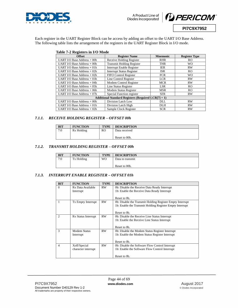
Page 44 of 69
PI7C9X7952 www.diodes.com August 2017
Document Number D40129 Rev 1-2 © Diodes Incorporated
All trademarks are property of their respective owners.
PI7C9X7952
Each register in the UART Register Block can be access by adding an offset to the UART I/O Base Address.
The following table lists the arrangement of the registers in the UART Register Block in I/O mode.
Table 7-2 Registers in I/O Mode Offset Register Name Mnemonic Register Type
UART I/O Base Address + 00h Receive Holding Register RHR RO
UART I/O Base Address + 00h Transmit Holding Register THR WO
UART I/O Base Address + 01h Interrupt Enable Register IER RW
UART I/O Base Address + 02h Interrupt Status Register ISR RO
UART I/O Base Address + 02h FIFO Control Register FCR WO
UART I/O Base Address + 03h Line Control Register LCR RW
UART I/O Base Address + 04h Modem Control Register MCR RW
UART I/O Base Address + 05h Line Status Register LSR RO
UART I/O Base Address + 06h Modem Status Register MSR RO
UART I/O Base Address + 07h Special Function register SFR RW
Additional Standard Registers (Required LCR[7] = 1)
UART I/O Base Address + 00h Division Latch Low DLL RW
UART I/O Base Address + 01h Division Latch High DLH RW
UART I/O Base Address + 02h Sample Clock Register SCR RW
7.1.1. RECEIVE HOLDING REGISTER – OFFSET 00h
BIT FUNCTION TYPE DESCRIPTION
7:0 Rx Holding RO Data received
Reset to 00h.
7.1.2. TRANSMIT HOLDING REGISTER – OFFSET 00h
BIT FUNCTION TYPE DESCRIPTION
7:0 Tx Holding WO Data to transmit
Reset to 00h.
7.1.3. INTERRUPT ENABLE REGISTER – OFFSET 01h
BIT FUNCTION TYPE DESCRIPTION
0 Rx Data Available
Interrupt
RW 0b: Disable the Receive Data Ready Interrupt
1b: Enable the Receive Data Ready Interrupt
Reset to 0b.
1 Tx Empty Interrupt RW 0b: Disable the Transmit Holding Register Empty Interrupt
1b: Enable the Transmit Holding Register Empty Interrupt
Reset to 0b.
2 Rx Status Interrupt RW 0b: Disable the Receive Line Status Interrupt
1b: Enable the Receive Line Status Interrupt
Reset to 0b.
3 Modem Status
Interrupt
RW 0b: Disable the Modem Status Register Interrupt
1b: Enable the Modem Status Register Interrupt
Reset to 0b.
4 Xoff/Special character interrupt
RW 0b: Disable the Software Flow Control Interrupt 1b: Enable the Software Flow Control Interrupt
Reset to 0b.

Page 45 of 69
PI7C9X7952 www.diodes.com August 2017
Document Number D40129 Rev 1-2 © Diodes Incorporated
All trademarks are property of their respective owners.
PI7C9X7952
BIT FUNCTION TYPE DESCRIPTION
5 RTS Interrupt RW 0b: Disable RTS/DTR Interrupt
1b: Enable RTS/DTR Interrupt
Reset to 0b.
6 CTS Interrupt RW 0b: Disable CTS/DSR interrupt
1b: Enable CTS/DSR interrupt
Reset to 0b.
7 Reserved RW
7.1.4. INTERRUPT STATUS REGISTER – OFFSET 02h
BIT FUNCTION TYPE DESCRIPTION
7:0 Interrupt Status RO 0b: An interrupt is pending
1b: No interrupt pending
Reset to C1h.
Priority
Level
Interrupt Status Bits Interrupt Source
BIT-7 BIT-6 BIT-5 BIT-4 BIT-3 BIT-2 BIT-1 BIT-0
1 1 1 0 0 0 1 1 0 Rx data error
2 1 1 0 0 0 1 0 0 Rx data available
3 1 1 0 0 1 1 0 0 Rx time-out
4 1 1 0 0 0 0 1 0 Tx FIFO empty
5 1 1 0 0 0 0 0 0 Modem status change
6 1 1 0 1 0 0 0 0 Xoff or special
character detected
7 1 1 1 0 0 0 0 0 CTS or RTS state changed
X 1 1 0 0 0 0 0 1 No interrupt pending
7.1.5. FIFO CONTROL REGISTER – OFFSET 02h
BIT FUNCTION TYPE DESCRIPTION
0 FIFO Mode Enable WO 0b: Disable the FIFO mode
1b: Enable the FIFO mode
Reset to 0b.
1 Rx FIFO Flush WO 0b: No action
1b: Reset the receive FIFO, self-clear after resetting the FIFO
Reset to 0b.
2 Tx FIFO Flush WO 0b: No action
1b: Reset the transmit FIFO, self-clear after resetting the FIFO
Reset to 0b.
3 Reserved WO Reset to 0b.
5:4 Tx Trigger Level WO In the Enhanced Mode.
00b: 16
01b: 32 10b: 64
11b: 112
Reset to 00b.
7:6 Rx Trigger Level WO In the Non-Enhanced mode
00b: 1
01b: 4 10b: 8
11b: 14
In the Enhanced mode
00b: 15
01b: 31 10b: 63
11b: 111
Reset to 00b.
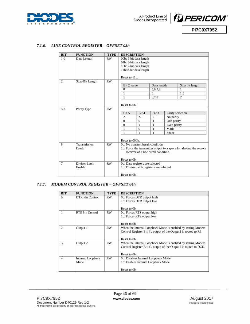
Page 46 of 69
PI7C9X7952 www.diodes.com August 2017
Document Number D40129 Rev 1-2 © Diodes Incorporated
All trademarks are property of their respective owners.
PI7C9X7952
7.1.6. LINE CONTROL REGISTER – OFFSET 03h
BIT FUNCTION TYPE DESCRIPTION
1:0 Data Length RW 00b: 5-bit data length
01b: 6-bit data length 10b: 7-bit data length
11b: 8-bit data length
Reset to 11b.
2 Stop-Bit Length RW
Bit 2 value Data length Stop bit length
0 5,6,7,8 1
1 5 1.5
1 6,7,8 2
Reset to 0b.
5:3 Parity Type RW
Bit 5 Bit 4 Bit 3 Parity selection
X X 0 No parity
0 0 1 Odd parity
0 1 1 Even parity
1 0 1 Mark
1 1 1 Space
Reset to 000b.
6 Transmission
Break
RW 0b: No transmit break condition
1b: Force the transmitter output to a space for alerting the remote receiver of a line break condition.
Reset to 0b.
7 Divisor Latch Enable
RW 0b: Data registers are selected 1b: Divisor latch registers are selected
Reset to 0b.
7.1.7. MODEM CONTROL REGISTER – OFFSET 04h
BIT FUNCTION TYPE DESCRIPTION
0 DTR Pin Control RW 0b: Forces DTR output high
1b: Forces DTR output low
Reset to 0b.
1 RTS Pin Control RW 0b: Forces RTS output high 1b: Forces RTS output low
Reset to 0b.
2 Output 1 RW When the Internal Loopback Mode is enabled by setting Modem Control Register Bit[4], output of the Output1 is routed to RI.
Reset to 0b.
3 Output 2 RW When the Internal Loopback Mode is enabled by setting Modem
Control Register Bit[4], output of the Output2 is routed to DCD.
Reset to 0b.
4 Internal Loopback
Mode
RW 0b: Disables Internal Loopback Mode
1b: Enables Internal Loopback Mode
Reset to 0b.

Page 47 of 69
PI7C9X7952 www.diodes.com August 2017
Document Number D40129 Rev 1-2 © Diodes Incorporated
All trademarks are property of their respective owners.
PI7C9X7952
BIT FUNCTION TYPE DESCRIPTION
5 AFE RW Autoflow Control Enable. When the AFE is enabled, autoflow
control is enabled. When it is disabled, the diagnostic mode is
enabled. In the diagnostic mode, transmitted data is immediately received.
When AFE is set to “1”, MCR Bit 1 is used to enable and disable the auto-RTS.
MCR Bit 5 (AFE)
MCR Bit 1 (RTS)
Configuration
1 1 Auto-RTS and auto-CTS are
enabled (autoflow control
enabled).
1 0 Only auto-CTS is enabled.
0 x Auto-RTS and auto-CTS are
disabled.
Reset to 0b.
6 Reserved Reset to 0b.
7 Enhanced
Transmission
RW 0b: Insert 1, 1.5 or 2 stop-bits between two transmitted
characters. 1b: Insert 0.5 stop-bits between two transmitted characters.
Note: Enabling feature may result in certain compatibility issues. This feature is only recommended when using two Pericom
UART devices.
Reset to 0b.
7.1.8. LINE STATUS REGISTER – OFFSET 05h
BIT FUNCTION TYPE DESCRIPTION
0 Rx Data Available RO 0b: No data in the receive FIFO 1b: Data in the receive FIFO
Reset to 0b.
1 Rx FIFO Overrun RO 0b: No overrun error 1b: Overrun error
Reset to 0b.
2 Rx Parity Error RO 0b: No parity error
1b: Parity error
Reset to 0b.
3 Rx Frame Error RO 0b: No framing error
1b: Framing error
Reset to 0b.
4 Rx Break Error RO 0b: No break condition
1b: Break condition
Reset to 0b.
5 Tx Empty RO 0b: Tx Holding Register is not empty.
1b: Tx Holding Register is empty.
Reset to 0b.
6 Tx Complete RO 0b: Tx Shift Register is not empty. 1b: Tx Shift Register is empty.
Reset to 0b.
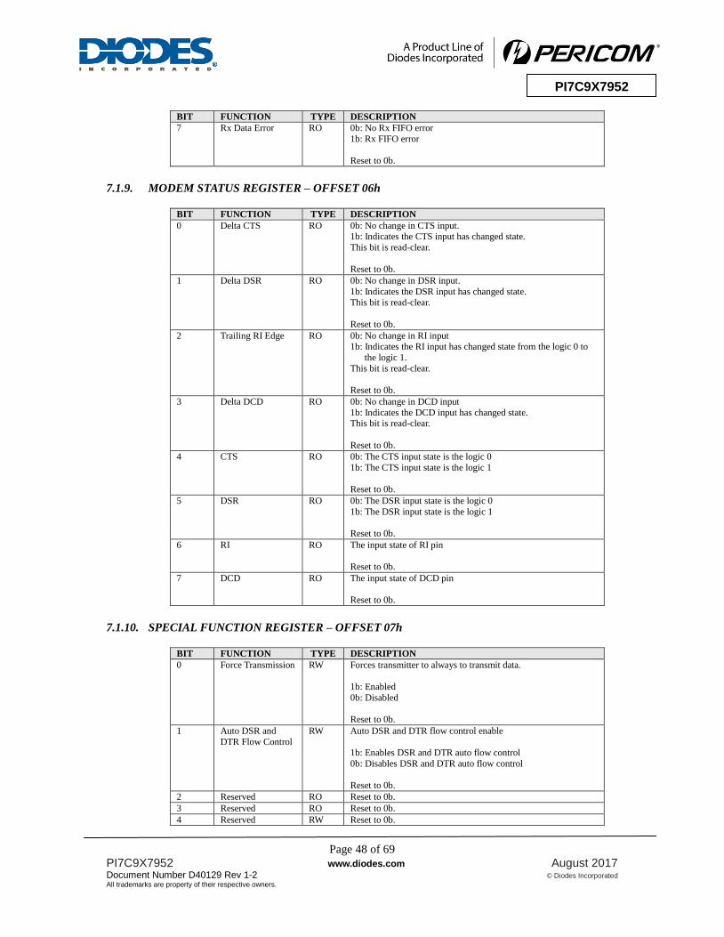
Page 48 of 69
PI7C9X7952 www.diodes.com August 2017
Document Number D40129 Rev 1-2 © Diodes Incorporated
All trademarks are property of their respective owners.
PI7C9X7952
BIT FUNCTION TYPE DESCRIPTION
7 Rx Data Error RO 0b: No Rx FIFO error
1b: Rx FIFO error
Reset to 0b.
7.1.9. MODEM STATUS REGISTER – OFFSET 06h
BIT FUNCTION TYPE DESCRIPTION
0 Delta CTS RO 0b: No change in CTS input. 1b: Indicates the CTS input has changed state.
This bit is read-clear.
Reset to 0b.
1 Delta DSR RO 0b: No change in DSR input.
1b: Indicates the DSR input has changed state.
This bit is read-clear.
Reset to 0b.
2 Trailing RI Edge RO 0b: No change in RI input 1b: Indicates the RI input has changed state from the logic 0 to
the logic 1.
This bit is read-clear.
Reset to 0b.
3 Delta DCD RO 0b: No change in DCD input
1b: Indicates the DCD input has changed state. This bit is read-clear.
Reset to 0b.
4 CTS RO 0b: The CTS input state is the logic 0
1b: The CTS input state is the logic 1
Reset to 0b.
5 DSR RO 0b: The DSR input state is the logic 0
1b: The DSR input state is the logic 1
Reset to 0b.
6 RI RO The input state of RI pin
Reset to 0b.
7 DCD RO The input state of DCD pin
Reset to 0b.
7.1.10. SPECIAL FUNCTION REGISTER – OFFSET 07h
BIT FUNCTION TYPE DESCRIPTION
0 Force Transmission RW Forces transmitter to always to transmit data.
1b: Enabled
0b: Disabled
Reset to 0b.
1 Auto DSR and
DTR Flow Control
RW Auto DSR and DTR flow control enable
1b: Enables DSR and DTR auto flow control
0b: Disables DSR and DTR auto flow control
Reset to 0b.
2 Reserved RO Reset to 0b.
3 Reserved RO Reset to 0b.
4 Reserved RW Reset to 0b.
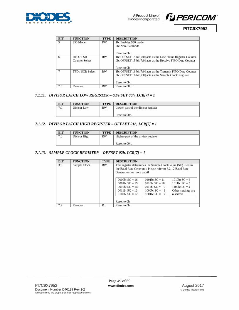
Page 49 of 69
PI7C9X7952 www.diodes.com August 2017
Document Number D40129 Rev 1-2 © Diodes Incorporated
All trademarks are property of their respective owners.
PI7C9X7952
BIT FUNCTION TYPE DESCRIPTION
5 950 Mode RW 1b: Enables 950 mode
0b: Non-950 mode
Reset to 0b.
6 RFD / LSR
Counter Select
RW 1b: OFFSET 15 bit[7:0] acts as the Line Status Register Counter
0b: OFFSET 15 bit[7:0] acts as the Receive FIFO Data Counter
Reset to 0b.
7 TFD / SCR Select RW 1b: OFFSET 16 bit[7:0] acts as the Transmit FIFO Data Counter
0b: OFFSET 16 bit[7:0] acts as the Sample Clock Register
Reset to 0b.
7:6 Reserved RW Reset to 00b.
7.1.11. DIVISOR LATCH LOW REGISTER – OFFSET 00h, LCR[7] = 1
BIT FUNCTION TYPE DESCRIPTION
7:0 Divisor Low RW Lower-part of the divisor register
Reset to 00h.
7.1.12. DIVISOR LATCH HIGH REGISTER – OFFSET 01h, LCR[7] = 1
BIT FUNCTION TYPE DESCRIPTION
7:0 Divisor High RW Higher-part of the divisor register
Reset to 00h.
7.1.13. SAMPLE CLOCK REGISTER – OFFSET 02h, LCR[7] = 1
BIT FUNCTION TYPE DESCRIPTION
3:0 Sample Clock RW This register determines the Sample Clock value (SC) used in
the Baud Rate Generator. Please refer to 5.2.12 Baud Rate Generation for more detail
0000b: SC = 16 0001b: SC = 15
0010b: SC = 14
0011b: SC = 13 0100b: SC = 12
0101b: SC = 11 0110b: SC = 10
0111b: SC = 9
1000b: SC = 8 1001b: SC = 7
1010b: SC = 6 1011b: SC = 5
1100b: SC = 4
Other settings are reserved.
Reset to 0h.
7:4 Reserve R Reset to 0h.

Page 50 of 69
PI7C9X7952 www.diodes.com August 2017
Document Number D40129 Rev 1-2 © Diodes Incorporated
All trademarks are property of their respective owners.
PI7C9X7952
7.2. REGISTERS IN MEMORY-MAPPING MODE
Each UART channel has a dedicated 512-byte register block in Memory mode. The register block can be
accessed by the UART Memory Base Address, which is obtained by adding the UART Register Offset to
the content of the Base Address Register 1 (BAR1). The following diagram shows the arrangement of
individual UART register blocks.
0000h
UART0 Registers
0200h
UART1 Registers
UART Memory Base Address
(BAR1 + UART Register Offset)
UART Register Offset
Figure 7-2 UART Register Block Arrangement in Memory Mode
Table 7-3 UART Base Address in Memory Mode UART UART I/O Base Address
UART0 BAR1 + 0000h
UART1 BAR1 + 0200h

Page 51 of 69
PI7C9X7952 www.diodes.com August 2017
Document Number D40129 Rev 1-2 © Diodes Incorporated
All trademarks are property of their respective owners.
PI7C9X7952
Each register in the UART Register Block can be access by adding an offset to the UART Memory Base
Address. The following table lists the arrangement of the registers in the UART Register Block in memory
mode.
Table 7-4 Memory-Map Mode Offset Register Name Mnemonic Register Type
UART Memory Base Address + 00h Receive Holding Register RHR RO
UART Memory Base Address + 00h Transmit Holding Register THR WO
UART Memory Base Address + 01h Interrupt Enable Register IER RW
UART Memory Base Address + 02h Interrupt Status Register ISR RO
UART Memory Base Address + 02h FIFO Control Register FCR WO
UART Memory Base Address + 04h Line Control Register LCR RW
UART Memory Base Address + 04h Modem Control Register MCR RW
UART Memory Base Address + 05h Line Status Register LSR RO
UART Memory Base Address + 06h Modem Status Register MSR RO
UART Memory Base Address + 07h Special Function Register SFR RW
UART Memory Base Address + 08h Divisor Latch Low DLL WO
UART Memory Base Address + 09h Divisor Latch High DLH WO
UART Memory Base Address + 0Ah Enhanced Function Register EFR RW
UART Memory Base Address + 0Bh XON 1 Character/Special
Character 1
XON1 RW
UART Memory Base Address + 0Ch XON 2 Character/Special Character 2
XON2 RW
UART Memory Base Address + 0Dh XOFF 1 Character/Special
Character 3
XOFF1 RW
UART Memory Base Address + 0Eh XOFF 2 Character/Special Character 3
XOFF2 RW
UART Memory Base Address + 0Fh ACR Register ASR RW
UART Memory Base Address + 10h Transmitter Interrupt Trigger
Level
TTL RW
UART Memory Base Address + 11h Receiver Interrupt Trigger Level RTL RW
UART Memory Base Address + 12h Automatic Flow control lower
trigger level
FCL RW
UART Memory Base Address + 13h Automatic Flow control lower
higher level
FCH RW
UART Memory Base Address + 14h Baud rate Prescale CPR RW
UART Memory Base Address + 15h Receive FIFO Data Counter /
Line Status Register Counter
RFD / LSR
Counter
RO
UART Memory Base Address + 16h Transmit FIFO Data Counter /
Sample Clock Register
TFD
Counter /
SCR
RW
UART Memory Base Address + 17h Global Register of LSR GLSR RW
UART Memory Base Address + 100h
~17Fh
UART0 FIFO DATA Register.
Use this register to map FIFO
data content.
FIFO_D RW
UART Memory Base Address + 180h ~1FFh
UART0 FIFO DATA LSR Register. Use this register to map
FIFO data relative LSR content.
FIFO_LSR RW
7.2.1. RECEIVE HOLDING REGISTER – OFFSET 00h
BIT FUNCTION TYPE DESCRIPTION
7:0 Rx Holding RO When data are read from the Receive Holding Register (RHR),
they are removed from the top of the receiver’s associated
FIFOs, which holds a queue of data received by the receiver.
Data read from the RHR when the FIFOs are empty are invalid.
The Line Status Register (LSR) indicates the full or empty status of the FIFOs.
Reset to 00h.
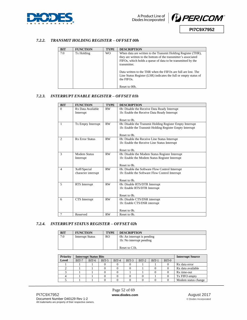
Page 52 of 69
PI7C9X7952 www.diodes.com August 2017
Document Number D40129 Rev 1-2 © Diodes Incorporated
All trademarks are property of their respective owners.
PI7C9X7952
7.2.2. TRANSMIT HOLDING REGISTER – OFFSET 00h
BIT FUNCTION TYPE DESCRIPTION
7:0 Tx Holding WO When data are written to the Transmit Holding Register (THR),
they are written to the bottom of the transmitter’s associated
FIFOs, which holds a queue of data to be transmitted by the transmitter.
Data written to the THR when the FIFOs are full are lost. The Line Status Register (LSR) indicates the full or empty status of
the FIFOs.
Reset to 00h.
7.2.3. INTERRUPT ENABLE REGISTER – OFFSET 01h
BIT FUNCTION TYPE DESCRIPTION
0 Rx Data Available Interrupt
RW 0b: Disable the Receive Data Ready Interrupt 1b: Enable the Receive Data Ready Interrupt
Reset to 0b.
1 Tx Empty Interrupt RW 0b: Disable the Transmit Holding Register Empty Interrupt
1b: Enable the Transmit Holding Register Empty Interrupt
Reset to 0b.
2 Rx Error Status RW 0b: Disable the Receive Line Status Interrupt
1b: Enable the Receive Line Status Interrupt
Reset to 0b.
3 Modem Status
Interrupt
RW 0b: Disable the Modem Status Register Interrupt
1b: Enable the Modem Status Register Interrupt
Reset to 0b.
4 Xoff/Special
character interrupt
RW 0b: Disable the Software Flow Control Interrupt
1b: Enable the Software Flow Control Interrupt
Reset to 0b.
5 RTS Interrupt RW 0b: Disable RTS/DTR Interrupt 1b: Enable RTS/DTR Interrupt
Reset to 0b.
6 CTS Interrupt RW 0b: Disable CTS/DSR interrupt
1b: Enable CTS/DSR interrupt
Reset to 0b.
7 Reserved RW Reset to 0b.
7.2.4. INTERRUPT STATUS REGISTER – OFFSET 02h
BIT FUNCTION TYPE DESCRIPTION
7:0 Interrupt Status RO 0b: An interrupt is pending 1b: No interrupt pending
Reset to C1h.
Priority
Level
Interrupt Status Bits Interrupt Source
BIT-7 BIT-6 BIT-5 BIT-4 BIT-3 BIT-2 BIT-1 BIT-0
1 1 1 0 0 0 1 1 0 Rx data error
2 1 1 0 0 0 1 0 0 Rx data available
3 1 1 0 0 1 1 0 0 Rx time-out
4 1 1 0 0 0 0 1 0 Tx FIFO empty
5 1 1 0 0 0 0 0 0 Modem status change

Page 53 of 69
PI7C9X7952 www.diodes.com August 2017
Document Number D40129 Rev 1-2 © Diodes Incorporated
All trademarks are property of their respective owners.
PI7C9X7952
6 1 1 0 1 0 0 0 0 Xoff or special character detected
7 1 1 1 0 0 0 0 0 CTS or RTS state
changed
X 1 1 0 0 0 0 0 1 No interrupt pending
7.2.5. FIFO CONTROL REGISTER – OFFSET 02h
BIT FUNCTION TYPE DESCRIPTION
0 FIFO Mode Enable WO 0b: Disable the FIFO mode
1b: Enable the FIFO mode
Reset to 0b.
1 Rx FIFO Flush WO 0b: No action 1b: Reset the receive FIFO, self-clear after resetting the FIFO
Reset to 0b.
2 Tx FIFO Flush WO 0b: No action 1b: Reset the transmit FIFO, self-clear after resetting the FIFO
Reset to 0b.
3 Reserved WO Reset to 0b
5:4 Tx Trigger Level WO In the Enhanced Mode:
00b: 16 01b: 32
10b: 64
11b: 112
Reset to 00b.
7:6 Rx Trigger Level WO In the Non-Enhanced mode 00b: 1
01b: 4
10b: 8 11b: 14
In the Enhanced mode 00b: 15
01b: 31
10b: 63 11b: 111
Reset to 00b.
7.2.6. LINE CONTROL REGISTER – OFFSET 03h
BIT FUNCTION TYPE DESCRIPTION
1:0 Data Length RW 00b: 5-bit data length 01b: 6-bit data length
10b: 7-bit data length
11b: 8-bit data length
Reset to 00b.
2 Stop-Bit Length RW
Bit 2 value Data length Stop bit length
0 5,6,7,8 1
1 5 1.5
1 6,7,8 2
Reset to 0b.
5:3 Parity Type RW
Bit 5 Bit 4 Bit 3 Parity selection
X X 0 No parity
0 0 1 Odd parity
0 1 1 Even parity
1 0 1 Mark
1 1 1 Space
Reset to 000b.
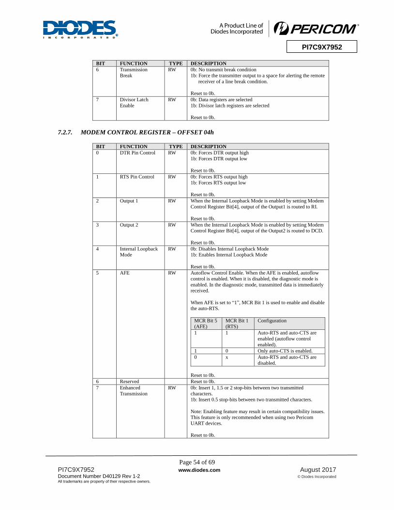
Page 54 of 69
PI7C9X7952 www.diodes.com August 2017
Document Number D40129 Rev 1-2 © Diodes Incorporated
All trademarks are property of their respective owners.
PI7C9X7952
BIT FUNCTION TYPE DESCRIPTION
6 Transmission
Break
RW 0b: No transmit break condition
1b: Force the transmitter output to a space for alerting the remote
receiver of a line break condition.
Reset to 0b.
7 Divisor Latch
Enable
RW 0b: Data registers are selected
1b: Divisor latch registers are selected
Reset to 0b.
7.2.7. MODEM CONTROL REGISTER – OFFSET 04h
BIT FUNCTION TYPE DESCRIPTION
0 DTR Pin Control RW 0b: Forces DTR output high
1b: Forces DTR output low
Reset to 0b.
1 RTS Pin Control RW 0b: Forces RTS output high
1b: Forces RTS output low
Reset to 0b.
2 Output 1 RW When the Internal Loopback Mode is enabled by setting Modem
Control Register Bit[4], output of the Output1 is routed to RI.
Reset to 0b.
3 Output 2 RW When the Internal Loopback Mode is enabled by setting Modem Control Register Bit[4], output of the Output2 is routed to DCD.
Reset to 0b.
4 Internal Loopback Mode
RW 0b: Disables Internal Loopback Mode 1b: Enables Internal Loopback Mode
Reset to 0b.
5 AFE RW Autoflow Control Enable. When the AFE is enabled, autoflow
control is enabled. When it is disabled, the diagnostic mode is
enabled. In the diagnostic mode, transmitted data is immediately received.
When AFE is set to “1”, MCR Bit 1 is used to enable and disable the auto-RTS.
MCR Bit 5 (AFE)
MCR Bit 1 (RTS)
Configuration
1 1 Auto-RTS and auto-CTS are
enabled (autoflow control
enabled).
1 0 Only auto-CTS is enabled.
0 x Auto-RTS and auto-CTS are
disabled.
Reset to 0b.
6 Reserved Reset to 0b.
7 Enhanced
Transmission
RW 0b: Insert 1, 1.5 or 2 stop-bits between two transmitted
characters.
1b: Insert 0.5 stop-bits between two transmitted characters.
Note: Enabling feature may result in certain compatibility issues. This feature is only recommended when using two Pericom
UART devices.
Reset to 0b.
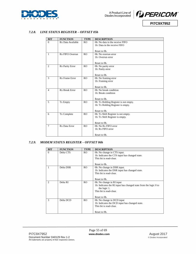
Page 55 of 69
PI7C9X7952 www.diodes.com August 2017
Document Number D40129 Rev 1-2 © Diodes Incorporated
All trademarks are property of their respective owners.
PI7C9X7952
7.2.8. LINE STATUS REGISTER – OFFSET 05h
BIT FUNCTION TYPE DESCRIPTION
0 Rx Data Available RO 0b: No data in the receive FIFO
1b: Data in the receive FIFO
Reset to 0b.
1 Rx FIFO Overrun RO 0b: No overrun error
1b: Overrun error
Reset to 0b.
2 Rx Parity Error RO 0b: No parity error 1b: Parity error
Reset to 0b.
3 Rx Frame Error RO 0b: No framing error 1b: Framing error
Reset to 0b.
4 Rx Break Error RO 0b: No break condition
1b: Break condition
Reset to 0b.
5 Tx Empty RO 0b: Tx Holding Register is not empty.
1b: Tx Holding Register is empty.
Reset to 0b.
6 Tx Complete RO 0b: Tx Shift Register is not empty.
1b: Tx Shift Register is empty.
Reset to 0b.
7 Rx Data Error RO 0b: No Rx FIFO error
1b: Rx FIFO error
Reset to 0b.
7.2.9. MODEM STATUS REGISTER – OFFSET 06h
BIT FUNCTION TYPE DESCRIPTION
0 Delta CTS RO 0b: No change in CTS input.
1b: Indicates the CTS input has changed state.
This bit is read-clear.
Reset to 0b.
1 Delta DSR RO 0b: No change in DSR input. 1b: Indicates the DSR input has changed state.
This bit is read-clear.
Reset to 0b.
2 Delta RI RO 0b: No change in RI input
1b: Indicates the RI input has changed state from the logic 0 to
the logic 1. This bit is read-clear.
Reset to 0b.
3 Delta DCD RO 0b: No change in DCD input
1b: Indicates the DCD input has changed state.
This bit is read-clear.
Reset to 0b.
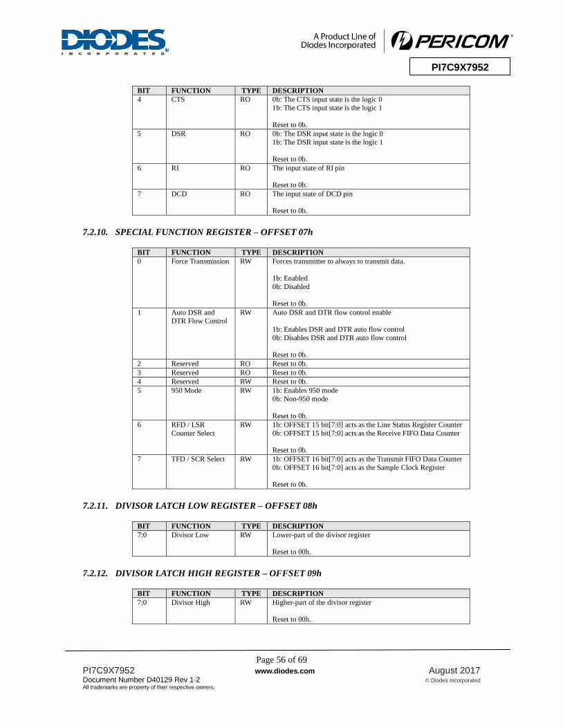
Page 56 of 69
PI7C9X7952 www.diodes.com August 2017
Document Number D40129 Rev 1-2 © Diodes Incorporated
All trademarks are property of their respective owners.
PI7C9X7952
BIT FUNCTION TYPE DESCRIPTION
4 CTS RO 0b: The CTS input state is the logic 0
1b: The CTS input state is the logic 1
Reset to 0b.
5 DSR RO 0b: The DSR input state is the logic 0
1b: The DSR input state is the logic 1
Reset to 0b.
6 RI RO The input state of RI pin
Reset to 0b.
7 DCD RO The input state of DCD pin
Reset to 0b.
7.2.10. SPECIAL FUNCTION REGISTER – OFFSET 07h
BIT FUNCTION TYPE DESCRIPTION
0 Force Transmission RW Forces transmitter to always to transmit data.
1b: Enabled
0b: Disabled
Reset to 0b.
1 Auto DSR and
DTR Flow Control
RW Auto DSR and DTR flow control enable
1b: Enables DSR and DTR auto flow control
0b: Disables DSR and DTR auto flow control
Reset to 0b.
2 Reserved RO Reset to 0b.
3 Reserved RO Reset to 0b.
4 Reserved RW Reset to 0b.
5 950 Mode RW 1b: Enables 950 mode 0b: Non-950 mode
Reset to 0b.
6 RFD / LSR
Counter Select
RW 1b: OFFSET 15 bit[7:0] acts as the Line Status Register Counter
0b: OFFSET 15 bit[7:0] acts as the Receive FIFO Data Counter
Reset to 0b.
7 TFD / SCR Select RW 1b: OFFSET 16 bit[7:0] acts as the Transmit FIFO Data Counter
0b: OFFSET 16 bit[7:0] acts as the Sample Clock Register
Reset to 0b.
7.2.11. DIVISOR LATCH LOW REGISTER – OFFSET 08h
BIT FUNCTION TYPE DESCRIPTION
7:0 Divisor Low RW Lower-part of the divisor register
Reset to 00h.
7.2.12. DIVISOR LATCH HIGH REGISTER – OFFSET 09h
BIT FUNCTION TYPE DESCRIPTION
7:0 Divisor High RW Higher-part of the divisor register
Reset to 00h.
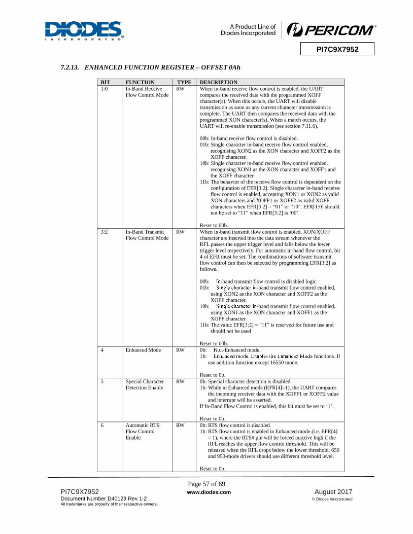
Page 57 of 69
PI7C9X7952 www.diodes.com August 2017
Document Number D40129 Rev 1-2 © Diodes Incorporated
All trademarks are property of their respective owners.
PI7C9X7952
7.2.13. ENHANCED FUNCTION REGISTER – OFFSET 0Ah
BIT FUNCTION TYPE DESCRIPTION
1:0 In-Band Receive
Flow Control Mode
RW When in-band receive flow control is enabled, the UART
compares the received data with the programmed XOFF
character(s). When this occurs, the UART will disable transmission as soon as any current character transmission is
complete. The UART then compares the received data with the
programmed XON character(s). When a match occurs, the UART will re-enable transmission (see section 7.11.6).
00b: In-band receive flow control is disabled.
01b: Single character in-band receive flow control enabled,
recognising XON2 as the XON character and XOFF2 as the XOFF character.
10b: Single character in-band receive flow control enabled,
recognising XON1 as the XON character and XOFF1 and the XOFF character.
11b: The behavior of the receive flow control is dependent on the
configuration of EFR[3:2]. Single character in-band receive flow control is enabled, accepting XON1 or XON2 as valid
XON characters and XOFF1 or XOFF2 as valid XOFF
characters when EFR[3:2] = “01” or “10”. EFR[1:0] should not be set to “11” when EFR[3:2] is ‘00’.
Reset to 00b.
3:2 In-Band Transmit Flow Control Mode
RW When in-band transmit flow control is enabled, XON/XOFF character are inserted into the data stream whenever the
RFL passes the upper trigger level and falls below the lower
trigger level respectively. For automatic in-band flow control, bit 4 of EFR must be set. The combinations of software transmit
flow control can then be selected by programming EFR[3:2] as
follows.
00b: -band transmit flow control is disabled logic. 01b: -band transmit flow control enabled,
using XON2 as the XON character and XOFF2 as the
XOFF character. 10b: -band transmit flow control enabled,
using XON1 as the XON character and XOFF1 as the
XOFF character. 11b: The value EFR[3:2] = “11” is reserved for future use and
should not be used
Reset to 00b.
4 Enhanced Mode RW 0b: -Enhanced mode.
1b: functions. If
use addition function except 16550 mode.
Reset to 0b.
5 Special Character Detection Enable
RW 0b: Special character detection is disabled. 1b: While in Enhanced mode (EFR[4]=1), the UART compares
the incoming receiver data with the XOFF1 or XOFF2 value
and interrupt will be asserted. If In-Band Flow Control is enabled, this bit must be set to ‘1’.
Reset to 0b.
6 Automatic RTS Flow Control
Enable
RW 0b: RTS flow control is disabled. 1b: RTS flow control is enabled in Enhanced mode (i.e. EFR[4]
= 1), where the RTS# pin will be forced inactive high if the RFL reaches the upper flow control threshold. This will be
released when the RFL drops below the lower threshold. 650
and 950-mode drivers should use different threshold level.
Reset to 0b.
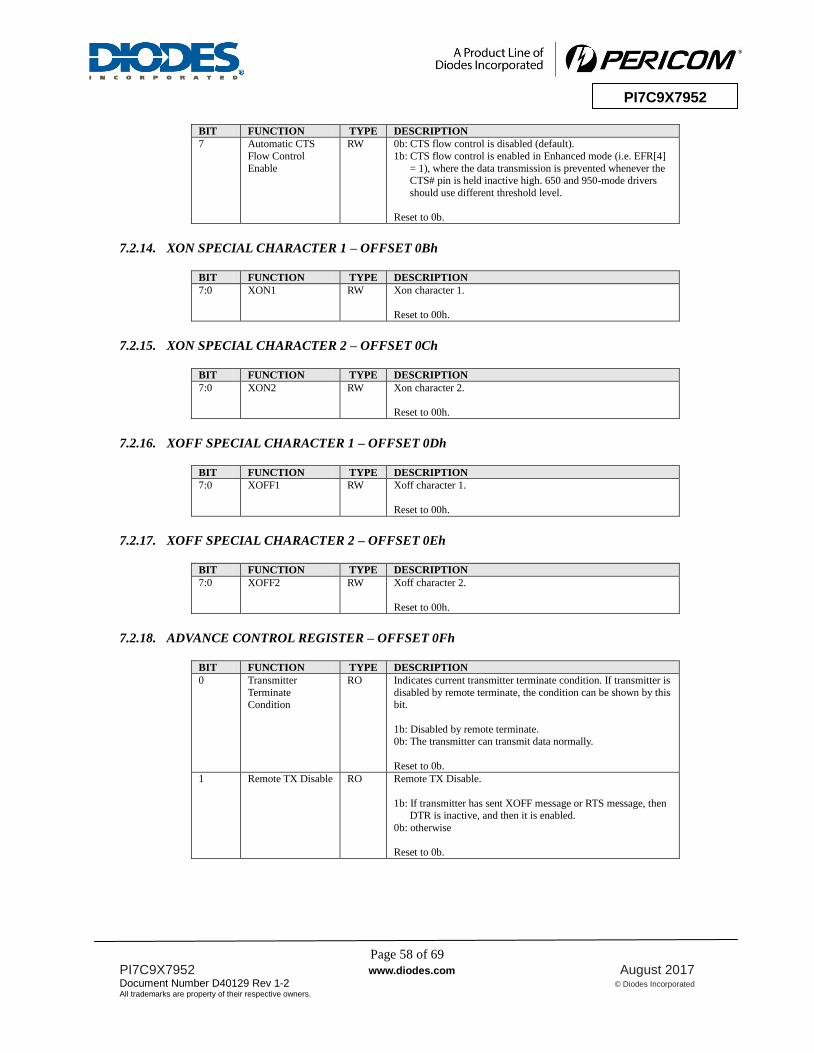
Page 58 of 69
PI7C9X7952 www.diodes.com August 2017
Document Number D40129 Rev 1-2 © Diodes Incorporated
All trademarks are property of their respective owners.
PI7C9X7952
BIT FUNCTION TYPE DESCRIPTION
7 Automatic CTS
Flow Control
Enable
RW 0b: CTS flow control is disabled (default).
1b: CTS flow control is enabled in Enhanced mode (i.e. EFR[4]
= 1), where the data transmission is prevented whenever the CTS# pin is held inactive high. 650 and 950-mode drivers
should use different threshold level.
Reset to 0b.
7.2.14. XON SPECIAL CHARACTER 1 – OFFSET 0Bh
BIT FUNCTION TYPE DESCRIPTION
7:0 XON1 RW Xon character 1.
Reset to 00h.
7.2.15. XON SPECIAL CHARACTER 2 – OFFSET 0Ch
BIT FUNCTION TYPE DESCRIPTION
7:0 XON2 RW Xon character 2.
Reset to 00h.
7.2.16. XOFF SPECIAL CHARACTER 1 – OFFSET 0Dh
BIT FUNCTION TYPE DESCRIPTION
7:0 XOFF1 RW Xoff character 1.
Reset to 00h.
7.2.17. XOFF SPECIAL CHARACTER 2 – OFFSET 0Eh
BIT FUNCTION TYPE DESCRIPTION
7:0 XOFF2 RW Xoff character 2.
Reset to 00h.
7.2.18. ADVANCE CONTROL REGISTER – OFFSET 0Fh
BIT FUNCTION TYPE DESCRIPTION
0 Transmitter
Terminate Condition
RO Indicates current transmitter terminate condition. If transmitter is
disabled by remote terminate, the condition can be shown by this bit.
1b: Disabled by remote terminate. 0b: The transmitter can transmit data normally.
Reset to 0b.
1 Remote TX Disable RO Remote TX Disable.
1b: If transmitter has sent XOFF message or RTS message, then DTR is inactive, and then it is enabled.
0b: otherwise
Reset to 0b.

Page 59 of 69
PI7C9X7952 www.diodes.com August 2017
Document Number D40129 Rev 1-2 © Diodes Incorporated
All trademarks are property of their respective owners.
PI7C9X7952
BIT FUNCTION TYPE DESCRIPTION
2 Xon/Xoff Detect RO When receiving a XON/XOFF character from a remote
transmitter, this bit is set to ‘1’. Otherwise, this bit is set to ‘0’.
The bit is read-clear. If the Xoff/Special Character Interrupt is enabled, the Xoff
Detect status is also reflected in the Interrupt Status Register
(Priority Level 6).
1b: Event true
0b: Event false
Reset to 0b.
3 Special Character Detect
RO When detecting the special characters from a remote transmitter, this bit is set to ‘1’. Otherwise, this bit is set to ‘0’.
The bit is read-clear.
If the Xoff/Special Character Interrupt is enabled, the status is also reflected in the Interrupt Status Register (Priority Level 6).
1b: Event true 0b: Event false
Reset to 0b.
7:4 Reserved RO Reset to 0000b.
7.2.19. TRANSMIT INTERRUPT TRIGGER LEVEL – OFFSET 10h
BIT FUNCTION TYPE DESCRIPTION
7:0 TTL RW Transmitter Interrupt Trigger Level.
Reset to 00h.
7.2.20. RECEIVE INTERRUPT TRIGGER LEVEL – OFFSET 11h
BIT FUNCTION TYPE DESCRIPTION
7:0 RTL RW Receiver Interrupt Trigger Level.
Reset to 00h.
7.2.21. FLOW CONTROL LOW TRIGGER LEVEL – OFFSET 12h
BIT FUNCTION TYPE DESCRIPTION
7:0 FCL RW Automatic Flow Control Low Trigger Level.
Reset to 00h.
7.2.22. FLOW CONTROL HIGH TRIGGER LEVEL – OFFSET 13h
BIT FUNCTION TYPE DESCRIPTION
7:0 FCH RW Automatic Flow Control High Trigger Level.
Reset to 00h.
7.2.23. CLOCK PRESCALE REGISTER – OFFSET 14h
BIT FUNCTION TYPE DESCRIPTION
3:0 CPRN RW N number in calculating the Prescaler, which is used to generate
the Baud Rate.
Reset to 0000b.

Page 60 of 69
PI7C9X7952 www.diodes.com August 2017
Document Number D40129 Rev 1-2 © Diodes Incorporated
All trademarks are property of their respective owners.
PI7C9X7952
BIT FUNCTION TYPE DESCRIPTION
7:4 CPRM RW M number in calculating the Prescaler, which is used to generate
the Baud Rate.
It is recommended that the value of the CPRM be set to “0000”, “0001” or “0010”.
Reset to 0000b.
7.2.24. RECEIVE FIFO DATA COUNTER – OFFSET 15h, SFR[6] = 0
The function of this register is selected by the Special Function Register (Offset 07h) bit 6. When SFR[6] is
set to ‘1’, this register functions as the Receive FIFO Data Counter. Otherwise, it functions as the Line
Status Register Counter.
BIT FUNCTION TYPE DESCRIPTION
7:0 Receive FIFO Data
Counter
RO The Receive FIFO Data Counter indicates the amount of data in
the Receive FIFO.
Reset to 00h.
7.2.25. LINE STATUS REGISTER COUNTER – OFFSET 15h, SFR[6] = 1
BIT FUNCTION TYPE DESCRIPTION
7:0 Line Status
Register Counter
RO The Line Status Register Counter indicates the amount of data in
the LSR.
Reset to 00h.
7.2.26. TRANSMIT FIFO DATA COUNTER – OFFSET 16h, SFR[7] = 1
The function of this register is selected by the Special Function Register (Offset 07h) bit 7. When SFR[7] is
set to ‘1’, this register functions as the Transmit FIFO Data Counter. Otherwise, it functions as the Sample
Clock Register.
BIT FUNCTION TYPE DESCRIPTION
7:0 Transmit FIFO Data Counter
RO The Transmit FIFO Data Counter indicates the amount of data in the Transmit FIFO.
Reset to 00h.
7.2.27. SAMPLE CLOCK REGISTER – OFFSET 16h, SFR[7] = 0
BIT FUNCTION TYPE DESCRIPTION
3:0 Sample Clock RW This register determines the Sample Clock value (SC) used in
the Baud Rate Generator. Please refer to 5.2.12 Baud Rate Generation for more detail
0000b: SC = 16
0001b: SC = 15 0010b: SC = 14
0011b: SC = 13
0100b: SC = 12
0101b: SC = 11
0110b: SC = 10 0111b: SC = 9
1000b: SC = 8
1001b: SC = 7
1010b: SC = 6
1011b: SC = 5 1100b: SC = 4
Other settings are
reserved.
Reset to 0h.
7:4 Reserved RO Reset to 0h.

Page 61 of 69
PI7C9X7952 www.diodes.com August 2017
Document Number D40129 Rev 1-2 © Diodes Incorporated
All trademarks are property of their respective owners.
PI7C9X7952
7.2.28. GLOBAL LINE STATUS REGISTER – OFFSET 17h
BIT FUNCTION TYPE DESCRIPTION
0 RX Data Available RO 0b: No data in the receive FIFO
1b: Data in the receive FIFO
Reset to 0b.
1 RX FIFO Overrun RO 0b: No overrun error
1b: Overrun error
Reset to 0b.
2 RX Parity Error RO 0b: No parity error 1b: Parity error
Reset to 0b.
3 RX Frame Error RO 0b: No framing error 1b: Framing error
Reset to 0b.
4 RX Break Error RO 0b: No break condition
1b: Break condition
Reset to 0b.
5 TX Empty RO 0b: Tx Holding Register is not empty.
1b: Tx Holding Register is empty.
Reset to 0b.
6 TX Complete RO 0b: Tx Shift Register is not empty.
1b: Tx Shift Register is empty.
Reset to 0b.
7 RX Data Error RO 0b: No Rx FIFO error
1b: Rx FIFO error
Reset to 0b.
7.2.29. RECEIVE FIFO DATA REGISTERS – OFFSET 100h ~ 17Fh
BIT FUNCTION TYPE DESCRIPTION
7:0 Receive FIFO Data RO This register is used to map RX FIFO data content.
Reset to 00h.
7.2.30. TRANSMIT FIFO DATA REGISTERS – OFFSET 100h ~ 17Fh
BIT FUNCTION TYPE DESCRIPTION
7:0 Transmit FIFO
Data
WO This register is used to map TX FIFO to memory space.
Reset to 00h.
7.2.31. LINE STATUS FIFO REGISTERS –OFFSET 180h ~ 1FFh
BIT FUNCTION TYPE DESCRIPTION
7:0 Line Status FIFO RO This register is used to map FIFO data relative LSR content.
Reset to 00h.
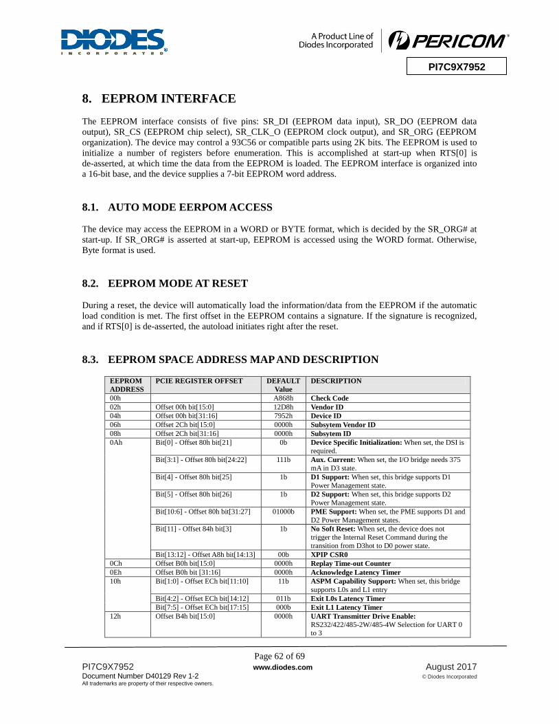
Page 62 of 69
PI7C9X7952 www.diodes.com August 2017
Document Number D40129 Rev 1-2 © Diodes Incorporated
All trademarks are property of their respective owners.
PI7C9X7952
8. EEPROM INTERFACE
The EEPROM interface consists of five pins: SR_DI (EEPROM data input), SR_DO (EEPROM data
output), SR_CS (EEPROM chip select), SR_CLK_O (EEPROM clock output), and SR_ORG (EEPROM
organization). The device may control a 93C56 or compatible parts using 2K bits. The EEPROM is used to
initialize a number of registers before enumeration. This is accomplished at start-up when RTS[0] is
de-asserted, at which time the data from the EEPROM is loaded. The EEPROM interface is organized into
a 16-bit base, and the device supplies a 7-bit EEPROM word address.
8.1. AUTO MODE EERPOM ACCESS
The device may access the EEPROM in a WORD or BYTE format, which is decided by the SR_ORG# at
start-up. If SR_ORG# is asserted at start-up, EEPROM is accessed using the WORD format. Otherwise,
Byte format is used.
8.2. EEPROM MODE AT RESET
During a reset, the device will automatically load the information/data from the EEPROM if the automatic
load condition is met. The first offset in the EEPROM contains a signature. If the signature is recognized,
and if RTS[0] is de-asserted, the autoload initiates right after the reset.
8.3. EEPROM SPACE ADDRESS MAP AND DESCRIPTION
EEPROM
ADDRESS
PCIE REGISTER OFFSET DEFAULT
Value
DESCRIPTION
00h A868h Check Code
02h Offset 00h bit[15:0] 12D8h Vendor ID
04h Offset 00h bit[31:16] 7952h Device ID
06h Offset 2Ch bit[15:0] 0000h Subsytem Vendor ID
08h Offset 2Ch bit[31:16] 0000h Subsytem ID
0Ah Bit[0] - Offset 80h bit[21] 0b Device Specific Initialization: When set, the DSI is
required.
Bit[3:1] - Offset 80h bit[24:22] 111b Aux. Current: When set, the I/O bridge needs 375
mA in D3 state.
Bit[4] - Offset 80h bit[25] 1b D1 Support: When set, this bridge supports D1
Power Management state.
Bit[5] - Offset 80h bit[26] 1b D2 Support: When set, this bridge supports D2
Power Management state.
Bit[10:6] - Offset 80h bit[31:27] 01000b PME Support: When set, the PME supports D1 and
D2 Power Management states.
Bit[11] - Offset 84h bit[3] 1b No Soft Reset: When set, the device does not
trigger the Internal Reset Command during the
transition from D3hot to D0 power state.
Bit[13:12] - Offset A8h bit[14:13] 00b XPIP CSR0
0Ch Offset B0h bit[15:0] 0000h Replay Time-out Counter
0Eh Offset B0h bit [31:16] 0000h Acknowledge Latency Timer
10h Bit[1:0] - Offset ECh bit[11:10] 11b ASPM Capability Support: When set, this bridge
supports L0s and L1 entry
Bit[4:2] - Offset ECh bit[14:12] 011b Exit L0s Latency Timer
Bit[7:5] - Offset ECh bit[17:15] 000b Exit L1 Latency Timer
12h Offset B4h bit[15:0] 0000h UART Transmitter Drive Enable: RS232/422/485-2W/485-4W Selection for UART 0 to 3
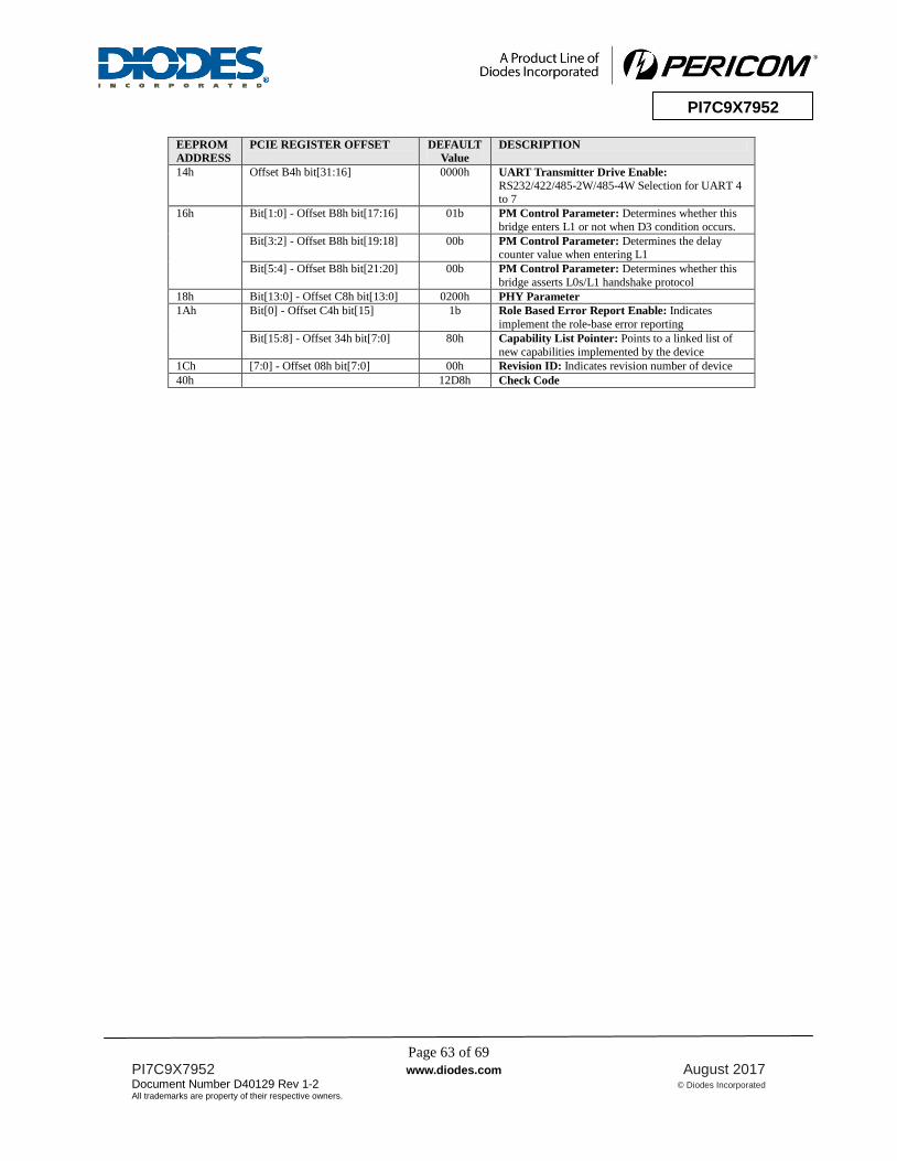
Page 63 of 69
PI7C9X7952 www.diodes.com August 2017
Document Number D40129 Rev 1-2 © Diodes Incorporated
All trademarks are property of their respective owners.
PI7C9X7952
EEPROM
ADDRESS
PCIE REGISTER OFFSET DEFAULT
Value
DESCRIPTION
14h Offset B4h bit[31:16] 0000h UART Transmitter Drive Enable:
RS232/422/485-2W/485-4W Selection for UART 4 to 7
16h Bit[1:0] - Offset B8h bit[17:16] 01b PM Control Parameter: Determines whether this
bridge enters L1 or not when D3 condition occurs.
Bit[3:2] - Offset B8h bit[19:18] 00b PM Control Parameter: Determines the delay counter value when entering L1
Bit[5:4] - Offset B8h bit[21:20] 00b PM Control Parameter: Determines whether this
bridge asserts L0s/L1 handshake protocol
18h Bit[13:0] - Offset C8h bit[13:0] 0200h PHY Parameter
1Ah Bit[0] - Offset C4h bit[15] 1b Role Based Error Report Enable: Indicates
implement the role-base error reporting
Bit[15:8] - Offset 34h bit[7:0] 80h Capability List Pointer: Points to a linked list of
new capabilities implemented by the device
1Ch [7:0] - Offset 08h bit[7:0] 00h Revision ID: Indicates revision number of device
40h 12D8h Check Code
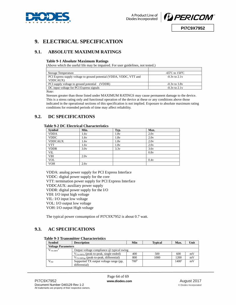
Page 64 of 69
PI7C9X7952 www.diodes.com August 2017
Document Number D40129 Rev 1-2 © Diodes Incorporated
All trademarks are property of their respective owners.
PI7C9X7952
9. ELECTRICAL SPECIFICATION
9.1. ABSOLUTE MAXIMUM RATINGS
Table 9-1 Absolute Maximum Ratings (Above which the useful life may be impaired. For user guidelines, not tested.)
Storage Temperature -65oC to 150oC
PCI Express supply voltage to ground potential (VDDA, VDDC, VTT and
VDDCAUX)
-0.3v to 2.1v
PCI supply voltage to ground potential (VDDR) -0.3v to 3.8v
DC input voltage for PCI Express signals -0.3v to 2.1v
Note:
Stresses greater than those listed under MAXIMUM RATINGS may cause permanent damage to the device.
This is a stress rating only and functional operation of the device at these or any conditions above those
indicated in the operational sections of this specification is not implied. Exposure to absolute maximum rating
conditions for extended periods of time may affect reliability.
9.2. DC SPECIFICATIONS
Table 9-2 DC Electrical Characteristics Symbol Min. Typ. Max.
VDDA 1.6v 1.8v 2.0v
VDDC 1.6v 1.8v 2.0v
VDDCAUX 1.6v 1.8v 2.0v
VTT 1.6v 1.8v 2.0v
VDDR 3.0v 3.3v 3.6v
VIL 0.8v
VIH 2.0v
VOL 0.4v
VOH 2.6v
VDDA: analog power supply for PCI Express Interface
VDDC: digital power supply for the core
VTT: termination power supply for PCI Express Interface
VDDCAUX: auxiliary power supply
VDDR: digital power supply for the I/O
VIH: I/O input high voltage
VIL: I/O input low voltage
VOL: I/O output low voltage
VOH: I/O output High voltage
The typical power consumption of PI7C9X7952 is about 0.7 watt.
9.3. AC SPECIFICATIONS
Table 9-3 Transmitter Characteristics Symbol Description Min Typical Max. Unit
Voltage Parameters
VTX-DIFFa Output voltage compliance @ typical swing
VTX-DIFFp (peak-to-peak, single ended) 400 500 600 mV
VTX-DIFFpp (peak-to-peak, differential) 800 1000 1200 mV
VSW Supported TX output voltage range (pp,
differential)
700b 1400c mV

Page 65 of 69
PI7C9X7952 www.diodes.com August 2017
Document Number D40129 Rev 1-2 © Diodes Incorporated
All trademarks are property of their respective owners.
PI7C9X7952
Symbol Description Min Typical Max. Unit
VOL Low-level output voltage VTT - 1.5 *VTX-DIFFp V
VOH High-level output voltage VTT - 0.5VTX-DIFFp V
VTX-CM-AC Transmit common-mode voltage in L0 0.50 VTT - VTX-DIFFp 1.45 V
VTX-CM-HiZ Transmit common-mode voltage in L0s
(TX) & L1
VTX-CM-AC V
VTX-DE-RATIO De-emphasized differential output
voltage
0 -7.96 dB
VTX-IDLE-DIFFp Electric Idle differential peak voltage 20 mV
VTX-RCV-DETECT Voltage change during Receive Detection
VTX-DIFFp mV
RLTX-DIFF Transmitter Differential Return loss 10 dB
RLTX-CM Transmitter Common Mode Return loss 6 dB
ZOSE Single-ended output impedance 40 50 60 Ω
ZTX-DIFF-DC DC Differential TX Impedance 80 100 120 Ω
TTX-RISE, TTX-FALL Rise / Fall time of TxP, TxN outputs 80 110d ps
Jitter Parameters
UI Unit Interval 399.88 400 400.12 ps
TTX-MAX-JITTER Transmitter total jitter (peak-to-peak) 0.30e UI
TTX-EYE Minimum TX Eye Width (1 - TTX-MAX-JITTER)
0.70 UI
TTX-EYE-MEDIAN-to-
MAX-JITTER
Maximum time between the jitter
median and
maximum deviation from the median
0.15 UI
Timing Parameters
LTLAT-10 Transmitter data latency (for n=10) 9 11 UI
LTLAT-20 Transmitter data latency (for n=20) 9 11 UI
LTX-SKEW Transmitter data skew between any 2
lanes
0 2 +
200ps
UI
TTX-IDLE-SET-TO-IDLE Maximum time to transition to a valid
electrical idle after sending an Electrical
Idle ordered set
8 ns
TEIExit Time to exit Electrical Idle (L0s) state into L0
12 16 ns
TBTEn Time from asserting BeaconTxEn to
beacon being transmitted on the lane
30 80 ns
a. Measured with Vtt = 1.2V, HiDrv=’0’,LowDrv=’0’ and Dtx=’0000’.
b. Minimum swing assumes LoDrv = 1, HiDrv = 0 and Dtx =1100
c. Max swing assumes LoDrv = 0, HiDrv = 1, Dtx = 0010, VTT = 1.8V d. As measured between 20% and 80% points. Will depend on package characteristics.
e. Measured using PCI Express Compliance Pattern
Table 9-4 Receiver Characteristics Symbol Description Min Typical Max. Unit
Voltage Parameters
VRX-DIFFp-p Differential input voltage
(peak-to-peak)
170 1200 mV
VRX-IDLE-DET-DIFFp-p Differential input threshold voltage (peak-to-peak) to assert
TxIdleDetect output
65 175 mV
VRX-CM-AC Receiver common-mode voltage for
AC-coupling
0 150 mV
TRX-RISE, TRX-FALL Rise time / Fall time of RxP, RxN
inputs
160 Ps
ZRX-DIFF-DC Differential input impedance (DC) 80 100 120 Ω
ZRX-COM-DC Single-ended input impedance 40 50 60 Ω
ZRX-COM-INITIAL-DC Initial input common mode impedance (DC)
5 50 60 Ω
ZRX-COM-HIGH-IMP-DC Powered down input common mode
impedance (DC)
200k Ω
RLRX-DIFF Receiver Differential Return Lossa 10 dB
RLRX-CM Receiver Common Mode Return
Lossb
6 dB
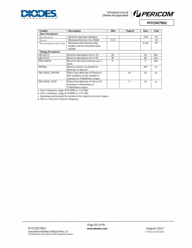
Page 66 of 69
PI7C9X7952 www.diodes.com August 2017
Document Number D40129 Rev 1-2 © Diodes Incorporated
All trademarks are property of their respective owners.
PI7C9X7952
Symbol Description Min Typical Max. Unit
Jitter Parameters
TRX-MAX-JITTER Receiver total jitter tolerance 0.65 UI
TRX-EYE Minimum Receiver Eye Width 0.35 UI
TRX-EYE-MEDIAN-to-MAX-JITTER Maximum time between jitter
median and max deviation from median
0.325 UI
Timing Parameters
LRLAT-10 Receiver data latency for n=10 28 29 bits
LRLAT-20 Receiver data latency for n=20 49 60 bits
TRX-SKEW Receiver data skew between any 2
lanes
0 1c bits
TBDDly Beacon-Activity on channel to
detection of Beacond
200 us
TRX-IDLE_ENTER Delay from detection of Electrical
Idle condition on the channel to
assertion of TxIdleDetect output
10 20 ns
TRX-IDLE_EXIT Delay from detection of L0s to L0
transition to deassertion of
TxIdleDetect output
5 10 ns
a. Over a frequency range of 50 MHz to 1.25 GHz. b. Over a frequency range of 50 MHz to 1.25 GHz.
c. Assuming synchronized bit streams at the respective receiver inputs.
d. This is a function of beacon frequency
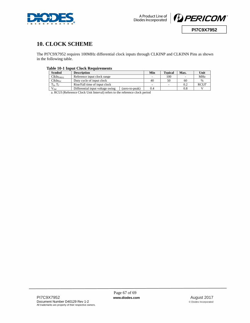
Page 67 of 69
PI7C9X7952 www.diodes.com August 2017
Document Number D40129 Rev 1-2 © Diodes Incorporated
All trademarks are property of their respective owners.
PI7C9X7952
10. CLOCK SCHEME
The PI7C9X7952 requires 100MHz differential clock inputs through CLKINP and CLKINN Pins as shown
in the following table.
Table 10-1 Input Clock Requirements Symbol Description Min Typical Max. Unit
ClkInFREQ Reference input clock range - 100 - MHz
ClkInDC Duty cycle of input clock 40 50 60 %
TR, TF Rise/Fall time of input clock - - 0.2 RCUIa
VSW Differential input voltage swing (zero-to-peak) 0.4 0.8 V
a. RCUI (Reference Clock Unit Interval) refers to the reference clock period
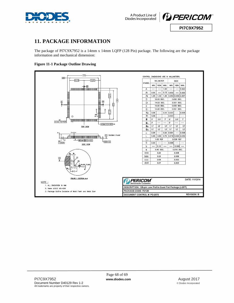
Page 68 of 69
PI7C9X7952 www.diodes.com August 2017
Document Number D40129 Rev 1-2 © Diodes Incorporated
All trademarks are property of their respective owners.
PI7C9X7952
11. PACKAGE INFORMATION
The package of PI7C9X7952 is a 14mm x 14mm LQFP (128 Pin) package. The following are the package
information and mechanical dimension:
Figure 11-1 Package Outline Drawing
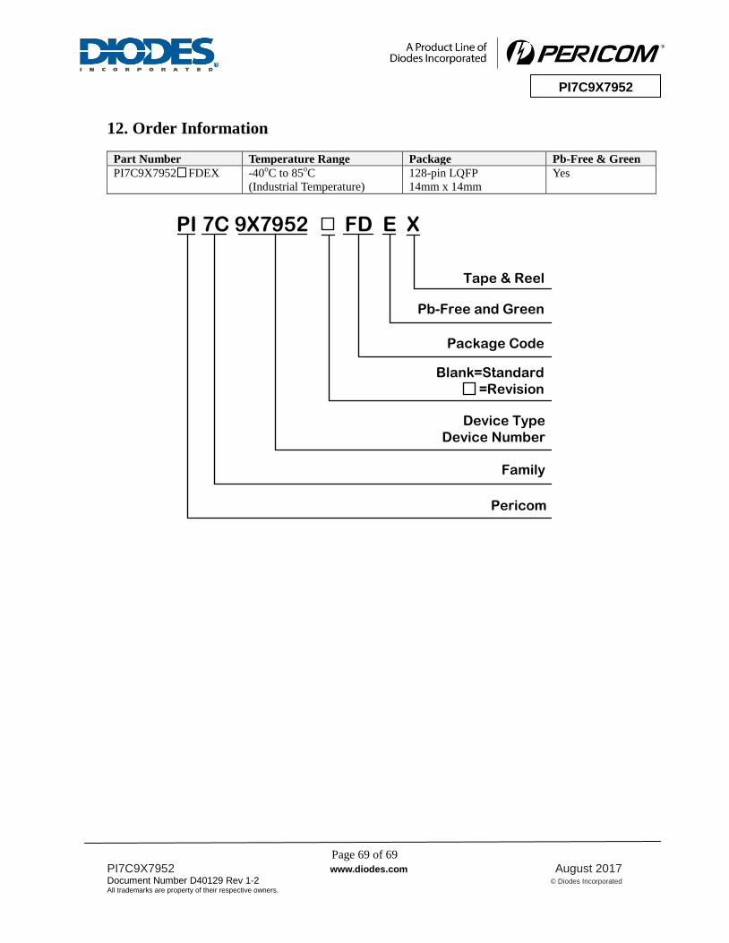
Page 69 of 69
PI7C9X7952 www.diodes.com August 2017
Document Number D40129 Rev 1-2 © Diodes Incorporated
All trademarks are property of their respective owners.
PI7C9X7952
12. Order Information
Part Number Temperature Range Package Pb-Free & Green
PI7C9X7952 FDEX -40oC to 85
oC
(Industrial Temperature)
128-pin LQFP
14mm x 14mm
Yes
PI 7C 9X7952 FD E X
Pb-Free and Green
Package Code
Device Type
Device Number
Pericom
Family
Blank=Standard
=Revision
Tape & Reel