Embed Size (px)
Citation preview

PI7C9X3G808GP PCI EXPRESS GEN 3 PACKET SWITCH
8-Port 8-Lane PCI Express Gen 3 Switch DATASHEET
REVISION 1
March 2021
1545 Barber Lane Milpitas, CA 95035
Telephone: 1-408-232-9100
FAX: 408-434-1040
Internet: http://www.diodes.com

PI7C9X3G808GP Page 2 of 315 March 2021
Document Number DS43471 Rev 1-2 www.diodes.com © Diodes Incorporated
PI7C9X3G808GP
IMPORTANT NOTICE
1. DIODES INCORPORATED AND ITS SUBSIDIARIES (“DIODES”) MAKE NO WARRANTY OF ANY KIND, EXPRESS OR
IMPLIED, WITH REGARDS TO ANY INFORMATION CONTAINED IN THIS DOCUMENT, INCLUDING, BUT NOT LIMITED TO, THE
IMPLIED WARRANTIES OF MERCHANTABILITY, FITNESS FOR A PARTICULAR PURPOSE OR NON-INFRINGEMENT OF THIRD
PARTY INTELLECTUAL PROPERTY RIGHTS (AND THEIR EQUIVALENTS UNDER THE LAWS OF ANY JURISDICTION).
2. The Information contained herein is for informational purpose only and is provided only to illustrate the operation of Diodes
products described herein and application examples. Diodes does not assume any liability arising out of the application or use of this
document or any product described herein. This document is intended for skilled and technically trained engineering customers and
users who design with Diodes products. Diodes products may be used to facilitate safety-related applications; however, in all instances
customers and users are responsible for (a) selecting the appropriate Diodes products for their applications, (b) evaluating the
suitability of the Diodes products for their intended applications, (c) ensuring their applications, which incorporate Diodes products,
comply the applicable legal and regulatory requirements as well as safety and functional-safety related standards, and (d) ensuring
they design with appropriate safeguards (including testing, validation, quality control techniques, redundancy, malfunction prevention,
and appropriate treatment for aging degradation) to minimize the risks associated with their applications.
3. Diodes assumes no liability for any application-related information, support, assistance or feedback that may be provided by
Diodes from time to time. Any customer or user of this document or products described herein will assume all risks and liabilities
associated with such use, and will hold Diodes and all companies whose products are represented herein or on Diodes’ websites,
harmless against all damages and liabilities.
4. Products described herein may be covered by one or more United States, international or foreign patents and pending patent
applications. Product names and markings noted herein may also be covered by one or more United States, international or foreign
trademarks and trademark applications. Diodes does not convey any license under any of its intellectual property rights or the rights of
any third parties (including third parties whose products and services may be described in this document or on Diodes’ website) under
this document.
5. Diodes products are provided subject to Diodes’ Standard Terms and Conditions of Sale
(https://www.diodes.com/about/company/terms-and-conditions/terms-and-conditions-of-sales/) or other applicable terms. This
document does not alter or expand the applicable warranties provided by Diodes. Diodes does not warrant or accept any liability
whatsoever in respect of any products purchased through unauthorized sales channel.
6. Diodes products and technology may not be used for or incorporated into any products or systems whose manufacture, use
or sale is prohibited under any applicable laws and regulations. Should customers or users use Diodes products in contravention of any
applicable laws or regulations, or for any unintended or unauthorized application, customers and users will (a) be solely responsible for
any damages, losses or penalties arising in connection therewith or as a result thereof, and (b) indemnify and hold Diodes and its
representatives and agents harmless against any and all claims, damages, expenses, and attorney fees arising out of, directly or
indirectly, any claim relating to any noncompliance with the applicable laws and regulations, as well as any unintended or unauthorized
application.
7. While efforts have been made to ensure the information contained in this document is accurate, complete and current, it may
contain technical inaccuracies, omissions and typographical errors. Diodes does not warrant that information contained in this
document is error-free and Diodes is under no obligation to update or otherwise correct this information. Notwithstanding the foregoing,
Diodes reserves the right to make modifications, enhancements, improvements, corrections or other changes without further notice to
this document and any product described herein. This document is written in English but may be translated into multiple languages for
reference. Only the English version of this document is the final and determinative format released by Diodes.
8. Any unauthorized copying, modification, distribution, transmission, display or other use of this document (or any portion
hereof) is prohibited. Diodes assumes no responsibility for any losses incurred by the customers or users or any third parties arising
from any such unauthorized use.
Copyright © 2021 Diodes Incorporated
www.diodes.com

PI7C9X3G808GP Page 3 of 315 March 2021
Document Number DS43471 Rev 1-2 www.diodes.com © Diodes Incorporated
PI7C9X3G808GP
REVISION HISTORY
Date Revision Number Description
03/08/2021 1 Initial Datasheet Release

PI7C9X3G808GP Page 4 of 315 March 2021
Document Number DS43471 Rev 1-2 www.diodes.com © Diodes Incorporated
PI7C9X3G808GP
TABLE OF CONTENTS
1 INTRODUCTION ......................................................................................................................................................... 23
1.1 KEY FEATURES ............................................................................................................................................ 24
2 GENERAL DESCRIPTION ......................................................................................................................................... 26
3 PIN DESCRIPTION ...................................................................................................................................................... 28
3.1 PCI EXPRESS INTERFACE SIGNALS ......................................................................................................... 28 3.2 CONFIGURATION STRAPPING SIGNALS ................................................................................................. 28 3.3 HOT PLUG SIGNALS .................................................................................................................................... 29 3.4 REFERENCE CLOCK OUTPUT AND CONTROL SIGNALS ..................................................................... 30 3.5 SIDE BAND MANAGEMENT SIGNALS...................................................................................................... 31 3.6 MISCELLANEOUS CONTROL AND STATUS SIGNALS .......................................................................... 31 3.7 JTAG BOUNDARY SCAN SIGNALS ........................................................................................................... 32 3.8 POWER PINS .................................................................................................................................................. 32
4 FUNCTIONAL OVERVIEW ....................................................................................................................................... 34
4.1 MODES OF OPERATIONS ............................................................................................................................ 34 4.1.1 BASE MODE (FAN-OUT MODE) ........................................................................................................... 34 4.1.2 CROSS-DOMAIN END-POINT MODE ................................................................................................... 34
4.2 PHYSICAL LAYER CIRCUITS ..................................................................................................................... 35 4.3 MEDIA ACCESS CONTROL (MAC)............................................................................................................. 35 4.4 DATA LINK LAYER (DLL) ........................................................................................................................... 36 4.5 TRANSACTION LAYER RECEIVE BLOCK (TLP DECAPSULATION) ................................................... 36 4.6 ROUTING ....................................................................................................................................................... 36 4.7 QUEUE ............................................................................................................................................................ 37
4.7.1 POSTED REQUEST HEADER (PH) ....................................................................................................... 37 4.7.2 POST REQUEST DATA (PD) .................................................................................................................. 37 4.7.3 NON-POSTED REQUEST HEADER AND DATA (NPHD) .................................................................... 37 4.7.4 COMPLETION HEADER (CPLH) .......................................................................................................... 37 4.7.5 COMPLETION DATA (CPLD) ................................................................................................................ 37
4.8 TRANSACTION ORDERING ........................................................................................................................ 38 4.9 PORT ARBITRATION.................................................................................................................................... 38 4.10 FLOW CONTROL ........................................................................................................................................... 39 4.11 TRANSATION LAYER TRANSMIT BLOCK (TLP ENCAPSULATION)................................................... 39 4.12 ACCESS CONTROL SERVICE (ACS) .......................................................................................................... 39 4.13 MULTICAST OPERATION ........................................................................................................................... 39
5 CHIP INITIZATION .................................................................................................................................................... 40
5.1 PORT-LANE CONFIGURATION .................................................................................................................. 40 5.1.1 MODE SELECTION ................................................................................................................................ 40 5.1.2 LANE MAPPING ..................................................................................................................................... 40 5.1.3 PORT NUMERING .................................................................................................................................. 40 5.1.4 PORT-LANE MAPPING .......................................................................................................................... 41
5.2 CLOCK SCHEME ........................................................................................................................................... 41 5.2.1 REFERENCE CLOCK OPERATION MODES ........................................................................................ 41 5.2.2 INTEGRATED REFERENCE CLOCK BUFFER .................................................................................... 42
5.3 EEPROM INTERFACE ................................................................................................................................... 43 5.3.1 EERPOM ACCESS MODES .................................................................................................................... 43 5.3.2 EEPROM MODE AT RESET ................................................................................................................... 43 5.3.3 EEPROM SPACE ADDRESS MAP.......................................................................................................... 43
5.4 SMBUS INTERFACE ..................................................................................................................................... 44

PI7C9X3G808GP Page 5 of 315 March 2021
Document Number DS43471 Rev 1-2 www.diodes.com © Diodes Incorporated
PI7C9X3G808GP
5.4.1 SMBUS BLOCK WRITE .......................................................................................................................... 45 5.4.2 SMBUS BLOCK READ ............................................................................................................................ 46 5.4.3 CSR READ, USING SMBUS BLOCK READ – BLOCK WRITE PROCESS CALL ................................. 49
5.5 I2C INTERFACE ............................................................................................................................................. 49 5.5.1 I2C REGISTER WRITE ACCESS ............................................................................................................. 50 5.5.2 I2C REGISTER READ ACCESS .............................................................................................................. 53
6 HOT PLUG SUPPORT ................................................................................................................................................. 56
6.1 HOT PLUG TYPES ......................................................................................................................................... 56 6.1.1 SURPRISED SERIAL HOT PLUG ........................................................................................................... 56 6.1.2 SURPRISED PARALLEL HOT PLUG ..................................................................................................... 57 6.1.3 MANAGED SERIAL HOT PLUG ............................................................................................................ 57
6.2 TIMING SEQUENCE FOR SURPRISED HOT PLUG OPERATION ........................................................... 58
7 CROSS-DOMAIN END-POINT .................................................................................................................................. 60
7.1 GENERAL DESCRIPTION ............................................................................................................................ 60 7.1.1 FAIL-OVER.............................................................................................................................................. 60 7.1.2 CO-PROCESSOR..................................................................................................................................... 60
7.2 PORT CONFIGURATION .............................................................................................................................. 61 7.3 BAR TRANSLATION FOR LOCAL HOST DOMAIN .................................................................................. 61
7.3.1 DIRECT ADDRESS TRANSLATION (DAT) ............................................................................................ 62 7.3.2 ADDRESS LOOK-UP TRANSLATION (ALUT)....................................................................................... 62 7.3.3 ID TRANSLATION ................................................................................................................................... 62
7.4 BAR TRANSLATION FOR PRIMARY HOST DOMAIN ............................................................................. 62 7.5 SCRATCHPADS AND DOORBELLS ........................................................................................................... 63
8 DIRECT MEMORY ACCESS ..................................................................................................................................... 64
8.1 GENERAL DESCRIPTION ............................................................................................................................ 64 8.2 DMA CONFIGURATION ............................................................................................................................... 64
8.2.1 DMA FUNCTIONS .................................................................................................................................. 64 8.2.1.1 DMA MODE BIT DEFINITION .......................................................................................................................... 65 8.2.1.2 DMA MODE AND CD MODE ............................................................................................................................ 65 8.2.1.3 ENUMERATION .................................................................................................................................................. 65
8.2.2 DMA CONTROL REGISTER ................................................................................................................... 65 8.2.2.1 DMA DESCRIPTOR REGISTER ......................................................................................................................... 66 8.2.2.2 DMA OPERATIONAL REGISTER ..................................................................................................................... 66
8.3 DMA DESCRIPTORS AND TRANSFERS .................................................................................................... 67 8.3.1 DESCRIPTORS ........................................................................................................................................ 67
8.3.1.1 INITIALIZATION ................................................................................................................................................ 67 8.3.1.2 OWNERSHIP ........................................................................................................................................................ 67 8.3.1.3 PRE-FETCH .......................................................................................................................................................... 68
8.3.2 TRANSFER .............................................................................................................................................. 68 8.3.2.1 LOCAL DOMAIN TRANSFER ........................................................................................................................... 68 8.3.2.2 CROSS DOMAIN TRANSFER ............................................................................................................................ 68
8.3.3 DESCRIPTOR LAYOUT .......................................................................................................................... 68 8.3.3.1 DOMAIN AND ADDRESS FIELD ...................................................................................................................... 69 8.3.3.2 TRANSFER COUNT FIELD ................................................................................................................................ 69 8.3.3.3 CONTROL FILED ................................................................................................................................................ 69 8.3.3.4 ERR FIELD ........................................................................................................................................................... 70 8.3.3.5 ST FIELD .............................................................................................................................................................. 70 8.3.3.6 CRC FIELD ........................................................................................................................................................... 71
8.4 ERROR REPORTING AND HANDLING ...................................................................................................... 71 8.4.1 ERROR REPORTING .............................................................................................................................. 71
8.4.1.1 REPORTING VIA FUNCTION ............................................................................................................................ 71 8.4.1.2 REPORTING VIA CHANNEL ............................................................................................................................. 71 8.4.1.3 REPORTING VIA DESCRIPTOR ....................................................................................................................... 71
8.4.2 ERROR LOGGING .................................................................................................................................. 72

PI7C9X3G808GP Page 6 of 315 March 2021
Document Number DS43471 Rev 1-2 www.diodes.com © Diodes Incorporated
PI7C9X3G808GP
8.4.3 DATA INTEGRITY ................................................................................................................................... 72 8.4.4 ERROR HANDLING FOR UNCORRECTABLE ERROR DETECTED ................................................... 72
8.4.4.1 ERROR IN DATA BUFFER ................................................................................................................................. 72 8.4.4.2 ERROR IN DESCRIPTOR ................................................................................................................................... 72
8.4.5 ERROR HANDLING FOR DMA READ ................................................................................................... 72
9 REGISTER DESCRIPTION ........................................................................................................................................ 73
9.1 REGISTER TYPES ......................................................................................................................................... 73 9.2 REGISTER ACCESS ....................................................................................................................................... 73
9.2.1 PCI-COMPATIBLE CONFIGURATION MECHANSIM ......................................................................... 73 9.2.2 PCI EXPRESS ENHANCED CONFIGURATION ACCESS MECHANISM ............................................ 73 9.2.3 DEVICE_SPECIFIC MEMORY MAPPED CONFIGURATION MECHANISM ..................................... 73
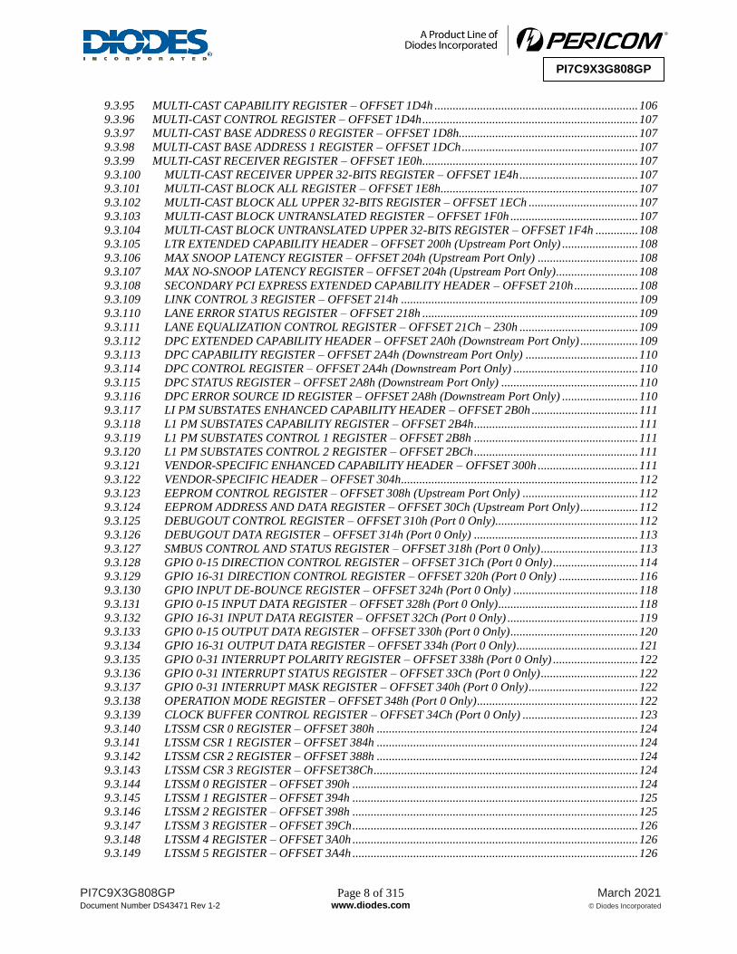
9.3 TRANSPARENT MODE CONFIGURATION REGISTERS ......................................................................... 75 9.3.1 VENDOR ID REGISTER – OFFSET 00h ................................................................................................ 80 9.3.2 DEVICE ID REGISTER – OFFSET 00h .................................................................................................. 80 9.3.3 COMMAND REGISTER – OFFSET 04h ................................................................................................. 80 9.3.4 PRIMARY STATUS REGISTER – OFFSET 04h ...................................................................................... 80 9.3.5 REVISION ID REGISTER – OFFSET 08h .............................................................................................. 81 9.3.6 CLASS REGISTER – OFFSET 08h .......................................................................................................... 81 9.3.7 CACHE LINE REGISTER – OFFSET 0Ch .............................................................................................. 81 9.3.8 PRIMARY LATENCY TIMER REGISTER – OFFSET 0Ch ..................................................................... 81 9.3.9 HEADER TYPE REGISTER – OFFSET 0Ch ........................................................................................... 81 9.3.10 BASE ADDRESS 0 REGISTER – OFFSET 10h (Upstream Port Only) ................................................... 82 9.3.11 BASE ADDRESS 1 REGISTER – OFFSET 14h (Upstream Port Only) ................................................... 82 9.3.12 PRIMARY BUS NUMBER REGISTER – OFFSET 18h ........................................................................... 82 9.3.13 SECONDARY BUS NUMBER REGISTER – OFFSET 18h ..................................................................... 82 9.3.14 SUBORDINATE BUS NUMBER REGISTER – OFFSET 18h ................................................................. 82 9.3.15 SECONDARY LATENCY TIMER REGISTER – OFFSET 18h ................................................................ 82 9.3.16 I/O BASE ADDRESS REGISTER – OFFSET 1Ch ................................................................................... 83 9.3.17 I/O LIMIT ADDRESS REGISTER – OFFSET 1Ch .................................................................................. 83 9.3.18 SECONDARY STATUS REGISTER – OFFSET 1Ch ............................................................................... 83 9.3.19 MEMORY BASE ADDRESS REGISTER – OFFSET 20h ........................................................................ 83 9.3.20 MEMORY LIMIT ADDRESS REGISTER – OFFSET 20h ....................................................................... 84 9.3.21 PREFETCHABLE MEMORY BASE ADDRESS REGISTER – OFFSET 24h .......................................... 84 9.3.22 PREFETCHABLE MEMORY LIMIT ADDRESS REGISTER – OFFSET 24h ......................................... 84 9.3.23 PREFETCHABLE MEMORY BASE ADDRESS UPPER 32-BITS REGISTER –OFFSET 28h ............... 84 9.3.24 PREFETCHABLE MEMORY LIMIT ADDRESS UPPER 32-BITS REGISTER – OFFSET 2Ch ............ 84 9.3.25 I/O BASE ADDRESS UPPER 16-BITS REGISTER – OFFSET 30h ........................................................ 85 9.3.26 I/O LIMIT ADDRESS UPPER 16-BITS REGISTER – OFFSET 30h ....................................................... 85 9.3.27 CAPABILITY POINTER REGISTER – OFFSET 34h .............................................................................. 85 9.3.28 INTERRUPT LINE REGISTER – OFFSET 3Ch ...................................................................................... 85 9.3.29 INTERRUPT PIN REGISTER – OFFSET 3Ch ........................................................................................ 85 9.3.30 BRIDGE CONTROL REGISTER – OFFSET 3Ch ................................................................................... 85 9.3.31 POWER MANAGEMENT CAPABILITIES REGISTER – OFFSET 40h .................................................. 86 9.3.32 POWER MANAGEMENT DATA REGISTER – OFFSET 44h ................................................................. 86 9.3.33 PPB SUPPORT EXTENSIONS REGISTER – OFFSET 44h .................................................................... 87 9.3.34 DATA REGISTER– OFFSET 44h ............................................................................................................ 87 9.3.35 MSI CAPABILITIES REGISTER – OFFSET 48h .................................................................................... 87 9.3.36 MESSAGE ADDRESS REGISTER – OFFSET 4Ch ................................................................................. 87 9.3.37 MESSAGE UPPER ADDRESS REGISTER – OFFSET 50h .................................................................... 87 9.3.38 MESSAGE DATA REGISTER – OFFSET 54h ......................................................................................... 88 9.3.39 MESSAGE MASK REGISTER – OFFSET 58h ........................................................................................ 88 9.3.40 MESSAGE PENDING REGISTER – OFFSET 5Ch ................................................................................. 88 9.3.41 PCI EXPRESS CAPABILITIES REGISTER – OFFSET 68h ................................................................... 88 9.3.42 DEVICE CAPABILITIES REGISTER – OFFSET 6Ch ............................................................................ 89

PI7C9X3G808GP Page 7 of 315 March 2021
Document Number DS43471 Rev 1-2 www.diodes.com © Diodes Incorporated
PI7C9X3G808GP
9.3.43 DEVICE CONTROL REGISTER – OFFSET 70h .................................................................................... 89 9.3.44 DEVICE STATUS REGISTER – OFFSET 70h ........................................................................................ 90 9.3.45 LINK CAPABILITIES REGISTER – OFFSET 74h .................................................................................. 90 9.3.46 LINK CONTROL REGISTER – OFFSET 78h ......................................................................................... 91 9.3.47 LINK STATUS REGISTER – OFFSET 78h .............................................................................................. 92 9.3.48 SLOT CAPABILITIES REGISTER – OFFSET 7Ch (Downstream Port Only) ........................................ 92 9.3.49 SLOT CONTROL REGISTER – OFFSET 80h (Downstream Port Only) ................................................ 93 9.3.50 SLOT STATUS REGISTER – OFFSET 80h (Downstream Port Only) .................................................... 93 9.3.51 DEVICE CAPABILITIES REGISTER 2 – OFFSET 8Ch ......................................................................... 94 9.3.52 DEVICE CONTROL REGISTER 2 – OFFSET 90h ................................................................................. 94 9.3.53 DEVICE STATUS REGISTER 2 – OFFSET 90h ..................................................................................... 95 9.3.54 LINK CAPABILITIES REGISTER 2 – OFFSET 94h ............................................................................... 95 9.3.55 LINK CONTROL REGISTER 2 – OFFSET 98h ...................................................................................... 95 9.3.56 LINK STATUS REGISTER 2 – OFFSET 98h ........................................................................................... 95 9.3.57 SLOT CAPABILITIES REGISTER 2 – OFFSET 9Ch .............................................................................. 96 9.3.58 SLOT CONTROL REGISTER 2 – OFFSET A0h...................................................................................... 96 9.3.59 SLOT STATUS REGISTER 2 – OFFSET A0h .......................................................................................... 96 9.3.60 SSID/SSVID CAPATILITIES REGISTER – OFFSET A4h ....................................................................... 96 9.3.61 SUBSYSTEM VENDOR ID REGISTER – OFFSET A8h ......................................................................... 96 9.3.62 SUBSYSTEM ID REGISTER – OFFSET A8h .......................................................................................... 96 9.3.63 MSI-X CAPATILITIES REGISTER – OFFSET B0h (Upstream Port Only) ............................................ 97 9.3.64 MSI-X TABLE OFFSET/TABLE BIR REGISTER – OFFSET B4h (Upstream Port Only) ...................... 97 9.3.65 MSI- X PBA OFFSET / PBA BIR REGISTER – OFFSET B8h (Upstream Port Only) ............................ 97 9.3.66 BAR 0 CONFIGURATION REGISTER – OFFSET E0h (Upstream Port Only) ...................................... 97 9.3.67 BAR 0-1 CONFIGURATION REGISTER – OFFSET E4h (Upstream Port Only)................................... 98 9.3.68 PCI EXPRESS ADVANCED ERROR REPORTING ENHANCED CAPABILITY HEADER REGISTER –
OFFSET 100h .......................................................................................................................................................... 98 9.3.69 UNCORRECTABLE ERROR STATUS REGISTER – OFFSET 104h ...................................................... 98 9.3.70 UNCORRECTABLE ERROR MASK REGISTER – OFFSET 108h.......................................................... 99 9.3.71 UNCORRECTABLE ERROR SEVERITY REGISTER – OFFSET 10Ch ................................................ 100 9.3.72 CORRECTABLE ERROR STATUS REGISTER – OFFSET 110h .......................................................... 101 9.3.73 CORRECTABLE ERROR MASK REGISTER – OFFSET 114h ............................................................. 101 9.3.74 ADVANCE ERROR CAPABILITIES AND CONTROL REGISTER – OFFSET 118h ............................ 101 9.3.75 HEADER LOG REGISTER – OFFSET From 11Ch to 128h ................................................................. 102 9.3.76 PCI EXPRESS VIRTUAL CHANNEL ENHANCED CAPABILITYHEADER REGISTER – OFFSET 130h
102 9.3.77 PORT VC CAPABILITY REGISTER 1 – OFFSET 134h........................................................................ 102 9.3.78 PORT VC CAPABILITY REGISTER 2 – OFFSET 138h........................................................................ 102 9.3.79 PORT VC CONTROL REGISTER – OFFSET 13Ch .............................................................................. 102 9.3.80 PORT VC STATUS REGISTER – OFFSET 13Ch .................................................................................. 103 9.3.81 VC RESOURCE CAPABILITY REGISTER (0) – OFFSET 140h ........................................................... 103 9.3.82 VC RESOURCE CONTROL REGISTER (0) – OFFSET 144h............................................................... 103 9.3.83 VC RESOURCE STATUS REGISTER (0) – OFFSET 148h ................................................................... 104 9.3.84 DEVICE SERIAL NUMBER ENHANCED CAPABILITY HEADER REGISTER – OFFSET 1A0h ....... 104 9.3.85 DEVICE SERIAL NUMBER LOWER DW REGISTER – OFFSET 1A4h .............................................. 104 9.3.86 DEVICE SERIAL NUMBER HIGHER DW REGISTER – OFFSET 1A8h ............................................. 104 9.3.87 PCI EXPRESS POWER BUDGETING ENHANCED CAPABILITY HEADER REGISTER – OFFSET
1B0h (Upstream Port Only) ................................................................................................................................... 104 9.3.88 DATA SELECT REGISTER – OFFSET 1B4h (Upstream Port Only) .................................................... 105 9.3.89 POWER BUDGETING DATA REGISTER – OFFSET 1B8h (Upstream Port Only) ............................. 105 9.3.90 POWER BUDGET CAPABILITY REGISTER – OFFSET 1BCh (Upstream Port Only) ....................... 105 9.3.91 ACS ENHANCED CAPABILITY HEADER REGISTER – OFFSET 1C0h (Downstream Port Only) .... 105 9.3.92 ACS CAPABILITY REGISTER – OFFSET 1C4h (Downstream Port Only) .......................................... 105 9.3.93 EGRESS CONTROL VECTOR REGISTER – OFFSET 1C8h (Downstream Port Only) ....................... 106 9.3.94 MULTI-CAST ENHANCED CAPABILITY HEADER REGISTER – OFFSET 1D0h ............................. 106
PI7C9X3G808GP Page 8 of 315 March 2021
Document Number DS43471 Rev 1-2 www.diodes.com © Diodes Incorporated
PI7C9X3G808GP
9.3.95 MULTI-CAST CAPABILITY REGISTER – OFFSET 1D4h ................................................................... 106 9.3.96 MULTI-CAST CONTROL REGISTER – OFFSET 1D4h ....................................................................... 107 9.3.97 MULTI-CAST BASE ADDRESS 0 REGISTER – OFFSET 1D8h........................................................... 107 9.3.98 MULTI-CAST BASE ADDRESS 1 REGISTER – OFFSET 1DCh .......................................................... 107 9.3.99 MULTI-CAST RECEIVER REGISTER – OFFSET 1E0h ....................................................................... 107 9.3.100 MULTI-CAST RECEIVER UPPER 32-BITS REGISTER – OFFSET 1E4h ....................................... 107 9.3.101 MULTI-CAST BLOCK ALL REGISTER – OFFSET 1E8h ................................................................. 107 9.3.102 MULTI-CAST BLOCK ALL UPPER 32-BITS REGISTER – OFFSET 1ECh .................................... 107 9.3.103 MULTI-CAST BLOCK UNTRANSLATED REGISTER – OFFSET 1F0h .......................................... 107 9.3.104 MULTI-CAST BLOCK UNTRANSLATED UPPER 32-BITS REGISTER – OFFSET 1F4h .............. 108 9.3.105 LTR EXTENDED CAPABILITY HEADER – OFFSET 200h (Upstream Port Only) ......................... 108 9.3.106 MAX SNOOP LATENCY REGISTER – OFFSET 204h (Upstream Port Only) ................................. 108 9.3.107 MAX NO-SNOOP LATENCY REGISTER – OFFSET 204h (Upstream Port Only) ........................... 108 9.3.108 SECONDARY PCI EXPRESS EXTENDED CAPABILITY HEADER – OFFSET 210h ..................... 108 9.3.109 LINK CONTROL 3 REGISTER – OFFSET 214h .............................................................................. 109 9.3.110 LANE ERROR STATUS REGISTER – OFFSET 218h ....................................................................... 109 9.3.111 LANE EQUALIZATION CONTROL REGISTER – OFFSET 21Ch – 230h ....................................... 109 9.3.112 DPC EXTENDED CAPABILITY HEADER – OFFSET 2A0h (Downstream Port Only) ................... 109 9.3.113 DPC CAPABILITY REGISTER – OFFSET 2A4h (Downstream Port Only) ..................................... 110 9.3.114 DPC CONTROL REGISTER – OFFSET 2A4h (Downstream Port Only) ......................................... 110 9.3.115 DPC STATUS REGISTER – OFFSET 2A8h (Downstream Port Only) ............................................. 110 9.3.116 DPC ERROR SOURCE ID REGISTER – OFFSET 2A8h (Downstream Port Only) ......................... 110 9.3.117 LI PM SUBSTATES ENHANCED CAPABILITY HEADER – OFFSET 2B0h ................................... 111 9.3.118 L1 PM SUBSTATES CAPABILITY REGISTER – OFFSET 2B4h ...................................................... 111 9.3.119 L1 PM SUBSTATES CONTROL 1 REGISTER – OFFSET 2B8h ...................................................... 111 9.3.120 L1 PM SUBSTATES CONTROL 2 REGISTER – OFFSET 2BCh ...................................................... 111 9.3.121 VENDOR-SPECIFIC ENHANCED CAPABILITY HEADER – OFFSET 300h ................................. 111 9.3.122 VENDOR-SPECIFIC HEADER – OFFSET 304h .............................................................................. 112 9.3.123 EEPROM CONTROL REGISTER – OFFSET 308h (Upstream Port Only) ...................................... 112 9.3.124 EEPROM ADDRESS AND DATA REGISTER – OFFSET 30Ch (Upstream Port Only) ................... 112 9.3.125 DEBUGOUT CONTROL REGISTER – OFFSET 310h (Port 0 Only)............................................... 112 9.3.126 DEBUGOUT DATA REGISTER – OFFSET 314h (Port 0 Only) ...................................................... 113 9.3.127 SMBUS CONTROL AND STATUS REGISTER – OFFSET 318h (Port 0 Only) ................................ 113 9.3.128 GPIO 0-15 DIRECTION CONTROL REGISTER – OFFSET 31Ch (Port 0 Only) ............................ 114 9.3.129 GPIO 16-31 DIRECTION CONTROL REGISTER – OFFSET 320h (Port 0 Only) .......................... 116 9.3.130 GPIO INPUT DE-BOUNCE REGISTER – OFFSET 324h (Port 0 Only) ......................................... 118 9.3.131 GPIO 0-15 INPUT DATA REGISTER – OFFSET 328h (Port 0 Only) .............................................. 118 9.3.132 GPIO 16-31 INPUT DATA REGISTER – OFFSET 32Ch (Port 0 Only) ........................................... 119 9.3.133 GPIO 0-15 OUTPUT DATA REGISTER – OFFSET 330h (Port 0 Only) .......................................... 120 9.3.134 GPIO 16-31 OUTPUT DATA REGISTER – OFFSET 334h (Port 0 Only) ........................................ 121 9.3.135 GPIO 0-31 INTERRUPT POLARITY REGISTER – OFFSET 338h (Port 0 Only) ............................ 122 9.3.136 GPIO 0-31 INTERRUPT STATUS REGISTER – OFFSET 33Ch (Port 0 Only) ................................ 122 9.3.137 GPIO 0-31 INTERRUPT MASK REGISTER – OFFSET 340h (Port 0 Only) .................................... 122 9.3.138 OPERATION MODE REGISTER – OFFSET 348h (Port 0 Only) ..................................................... 122 9.3.139 CLOCK BUFFER CONTROL REGISTER – OFFSET 34Ch (Port 0 Only) ...................................... 123 9.3.140 LTSSM CSR 0 REGISTER – OFFSET 380h ...................................................................................... 124 9.3.141 LTSSM CSR 1 REGISTER – OFFSET 384h ...................................................................................... 124 9.3.142 LTSSM CSR 2 REGISTER – OFFSET 388h ...................................................................................... 124 9.3.143 LTSSM CSR 3 REGISTER – OFFSET38Ch ....................................................................................... 124 9.3.144 LTSSM 0 REGISTER – OFFSET 390h .............................................................................................. 124 9.3.145 LTSSM 1 REGISTER – OFFSET 394h .............................................................................................. 125 9.3.146 LTSSM 2 REGISTER – OFFSET 398h .............................................................................................. 125 9.3.147 LTSSM 3 REGISTER – OFFSET 39Ch .............................................................................................. 126 9.3.148 LTSSM 4 REGISTER – OFFSET 3A0h .............................................................................................. 126 9.3.149 LTSSM 5 REGISTER – OFFSET 3A4h .............................................................................................. 126
PI7C9X3G808GP Page 9 of 315 March 2021
Document Number DS43471 Rev 1-2 www.diodes.com © Diodes Incorporated
PI7C9X3G808GP
9.3.150 LTSSM 6 REGISTER – OFFSET 3A8h .............................................................................................. 126 9.3.151 LTSSM 7 REGISTER – OFFSET 3ACh ............................................................................................. 126 9.3.152 LTSSM 8 REGISTER – OFFSET 3B0h .............................................................................................. 127 9.3.153 LTSSM 9 REGISTER – OFFSET 3B4h .............................................................................................. 128 9.3.154 LTSSM 10 REGISTER – OFFSET 3B8h ............................................................................................ 128 9.3.155 LTSSM 11 REGISTER – OFFSET 3BCh ........................................................................................... 128 9.3.156 LTSSM 12 REGISTER – OFFSET 3C0h ............................................................................................ 128 9.3.157 LTSSM 13 REGISTER – OFFSET 3C4h ............................................................................................ 129 9.3.158 LTSSM 14 REGISTER – OFFSET 3C8h ............................................................................................ 129 9.3.159 LTSSM 15 REGISTER – OFFSET 3CCh ........................................................................................... 130 9.3.160 DLL CSR 0 REGISTER – OFFSET 420h ........................................................................................... 130 9.3.161 DLL CSR 1 REGISTER – OFFSET 424h ........................................................................................... 130 9.3.162 DLL CSR 2 REGISTER – OFFSET 428h ........................................................................................... 131 9.3.163 DLL CSR 3 REGISTER – OFFSET 42Ch .......................................................................................... 131 9.3.164 DLL CSR 4 REGISTER – OFFSET 430h ........................................................................................... 131 9.3.165 DLL CSR 5 REGISTER – OFFSET 434h ........................................................................................... 131 9.3.166 DLL CSR 6 REGISTER – OFFSET 438h ........................................................................................... 132 9.3.167 DLL CSR 7 REGISTER – OFFSET 43Ch .......................................................................................... 132 9.3.168 DLL CSR 8 REGISTER – OFFSET 440h ........................................................................................... 133 9.3.169 DLL CSR 9 REGISTER – OFFSET 444h ........................................................................................... 133 9.3.170 DLL CSR 10 REGISTER – OFFSET 448h ......................................................................................... 134 9.3.171 DLL CSR 11 REGISTER – OFFSET 44Ch ........................................................................................ 134 9.3.172 DLL CSR 12 REGISTER – OFFSET 450h ......................................................................................... 134 9.3.173 DLL CSR 13 REGISTER – OFFSET 454h ......................................................................................... 134 9.3.174 DLL CSR 14 REGISTER – OFFSET 458h ......................................................................................... 135 9.3.175 DLL CSR 15 REGISTER – OFFSET 45Ch ........................................................................................ 135 9.3.176 DLL CSR 16 REGISTER – OFFSET 460h ......................................................................................... 136 9.3.177 DLL CSR 17 REGISTER – OFFSET 464h ......................................................................................... 136 9.3.178 DLL CSR 18 REGISTER – OFFSET 468h ......................................................................................... 136 9.3.179 DLL CSR 19 REGISTER – OFFSET 46Ch ........................................................................................ 136 9.3.180 LA DEBUG REGISTER – OFFSET 470h .......................................................................................... 136 9.3.181 TL CSR 0 REGISTER – OFFSET 4C0h ............................................................................................. 136 9.3.182 TL CSR 1 REGISTER – OFFSET 4C4h ............................................................................................. 137 9.3.183 TL CSR 2 REGISTER – OFFSET 4C8h ............................................................................................. 138 9.3.184 TL CSR 3 REGISTER – OFFSET 4CCh (Port 0 Only) ...................................................................... 138 9.3.185 TL CSR 4 REGISTER – OFFSET 4D0h ............................................................................................. 138 9.3.186 DEVICE CONFIGURATION 0 REGISTER – OFFSET 504h (Port 0 Only) ..................................... 138 9.3.187 DEVICE CONFIGURATION 1 REGISTER – OFFSET 508h (Port 0 Only) ..................................... 139 9.3.188 DEVICE CONFIGURATION 2 REGISTER – OFFSET 50Ch (Port 0 Only) .................................... 139 9.3.189 DEVICE CLOCK EXTERNAL CONTROL REGISTER – OFFSET 510h (Port 0 Only) .................... 140 9.3.190 DEVICE SRIS MODE EXTERNAL CONTROL REGISTER – OFFSET 514h (Port 0 Only) ............ 140 9.3.191 DEVICE COMM REFCLK MODE EXTERNAL CONTROL REGISTER – OFFSET 518h (Port 0 Only)
140 9.3.192 MBIST CFG CONTROL REGISTER – OFFSET 51Ch (Port 0 Only) ............................................... 141 9.3.193 MBIST CFG STATUS REGISTER – OFFSET 520h (Port 0 Only) .................................................... 141 9.3.194 NOC BIST CONTROL REGISTER – OFFSET 524h (Port 0 Only) ................................................... 141 9.3.195 EXTERNAL LOOPBACK PRBS CONTROL REGISTER – OFFSET 528h (Port 0 Only) ................. 141 9.3.196 PHY SRAM PROGRAM 0 REGISER – OFFSET 52Ch (Port 0 Only) ............................................... 142 9.3.197 PHY SRAM PROGRAM 1 REGISTER – OFFSET 530h (Port 0 Only) ............................................. 142 9.3.198 FAILOVER CONTROL REGISTER – OFFSET 534h (Port 0 Only) ................................................. 142 9.3.199 THERMAL SENSOR INT MASK AND STATUS REGISTER – OFFSET 538h (Port 0 Only) ........... 143 9.3.200 THERMAL SENSOR CONTROL REGISTER – OFFSET 53Ch (Port 0 Only) .................................. 143 9.3.201 DEVICE ELASTIC BUFFER EMPTY MODE EXTERNAL CONTROL REGISTER – OFFSET 540h
(Port 0 Only) .......................................................................................................................................................... 143 9.3.202 DEVICE MISC REGISTER – OFFSET 544h (Port 0 Only) .............................................................. 144

PI7C9X3G808GP Page 10 of 315 March 2021
Document Number DS43471 Rev 1-2 www.diodes.com © Diodes Incorporated
PI7C9X3G808GP
9.3.203 SWITCH DOMAIN MODE CONTROL REGISTER – OFFSET 558h (Port 0 Only) ......................... 144 9.3.204 PORT CLOCK CONTROL REGISTER – OFFSET 55Ch (Port 0 Only) ........................................... 144 9.3.205 PERFORMANCE COUNTER CONTROL REGISTER – OFFSET 56Ch .......................................... 144 9.3.206 PHY SOURCE SELECT REGISTER – OFFSET 570h....................................................................... 144 9.3.207 NIC CTRL 0 REGISTER – OFFSET 5A0h (Port 0 Only) .................................................................. 145 9.3.208 NIC CTRL 1 REGISTER – OFFSET 5A4h (Port 0 Only) .................................................................. 145 9.3.209 NIC CTRL 2 REGISTER – OFFSET 5A8h (Port 0 Only) .................................................................. 145 9.3.210 NIC CTRL 3 REGISTER – OFFSET 5ACh (Port 0 Only) .................................................................. 145 9.3.211 NIC CTRL 4 REGISTER – OFFSET 5B0h (Port 0 Only) .................................................................. 145 9.3.212 CR RW CTRL AND STATUS REGISTER – OFFSET 5C0h (Port 0 Only) ........................................ 146 9.3.213 CR CTRL 0 REGISTER – OFFSET 5C4h (Port 0 Only) .................................................................... 146 9.3.214 CR CTRL 1 REGISTER – OFFSET 5C8h (Port 0 Only) .................................................................... 146 9.3.215 CR CTRL 2 REGISTER – OFFSET 5CCh (Port 0 Only) ................................................................... 146 9.3.216 CR CTRL 3 REGISTER – OFFSET 5D0h (Port 0 Only) ................................................................... 146 9.3.217 THERMAL SENSOR TEST REGISTER – OFFSET 5D4h (Port 0 Only) ........................................... 146 9.3.218 THERMAL SENSOR CTRL 0 REGISTER – OFFSET 5D8h (Port 0 Only) ....................................... 147 9.3.219 THERMAL SENSOR CTRL 1 REGISTER – OFFSET 5DCh (Port 0 Only) ....................................... 147 9.3.220 THERMAL SENSOR CTRL 2 REGISTER – OFFSET 5E0h (Port 0 Only) ........................................ 148 9.3.221 INGRESS COMPLETION TLP PACKET COUNT[31:0] REGISTER – OFFSET 600h ................... 148 9.3.222 INGRESS COMPLETION TLP PACKET COUNT[47:32] REGISTER – OFFSET 604h ................. 149 9.3.223 INGRESS COMPLETION TLP PAYLOAD BYTE COUNT[31:0] REGISTER – OFFSET 608h ...... 149 9.3.224 INGRESS COMPLETION TLP PAYLOAD BYTE COUNT[47:32] REGITER – OFFSET 60Ch ...... 149 9.3.225 INGRESS POST TLP PACKET COUNT[31:0] REGISTER – OFFSET 610h ................................... 149 9.3.226 INGRESS POST TLP PACKET COUNT[47:32] REGISTER – OFFSET 614h ................................. 149 9.3.227 INGRESS POST TLP PAYLOAD BYTE COUNT[31:0] REGISTER – OFFSET 618h ...................... 149 9.3.228 INGRESS POST TLP PAYLOAD BYTE COUNT[47:32] REGISTER – OFFSET 61Ch ................... 150 9.3.229 INGRESS BAD TLP PACKET COUNT[31:0] REGISTER – OFFSET 620h ..................................... 150 9.3.230 INGRESS NON-POST TLP PACKET COUNT[31:0] REGISTER – OFFSET 628h ......................... 150 9.3.231 INGRESS NON-POST TLP PACKET COUNT[47:32] REGISTER – OFFSET 62Ch ....................... 150 9.3.232 EGRESS COMPLETION TLP PACKET COUNT[31:0] REGISTER - OFFSET 630h ...................... 150 9.3.233 EGRESS COMPLETION TLP PACKET COUNT[47:32] REGISTER – OFFSET 634h ................... 150 9.3.234 EGRESS COMPLETION TLP PAYLOAD BYTE COUNT[31:0] REGISTER – OFFSET 638h ........ 151 9.3.235 EGRESS COMPLETION TLP PAYLOAD BYTE COUNT[47:32] REGISTER – OFFSET 63Ch ..... 151 9.3.236 EGRESS POST TLP PACKET COUNT[31:0] REGISTER – OFFSET 640h .................................... 151 9.3.237 EGRESS POST TLP PACKET BYTE COUNT[47:32] REGISTER – OFFSET 644h ........................ 151 9.3.238 EGRESS POST TLP PAYLOAD BYTE COUNT[31:0] REGISTER – OFFSET 648h ....................... 151 9.3.239 EGRESS POST TLP PAYLOAD BYTE COUNT[47:32] REGISTER – OFFSET 64Ch ..................... 151 9.3.240 EGRESS ERROR TLP PACKET COUNT[15:0] REGISTER – OFFSET 650h ................................. 152 9.3.241 EGRESS ERROR TLP PAYLOAD BYTE COUNT[47:32] REGISTER – OFFSET 654h .................. 152 9.3.242 EGRESS NON-POST TLP PACKET COUNT[31:0] REGISTER – OFFSET 658h ........................... 152 9.3.243 EGRESS NON-POST TLP PACKET COUNT[47:32] REGISTER – OFFSET 65Ch ........................ 152 9.3.244 TL/DLL/MAC/PHY ERROR TYPE SEL REGISTER – OFFSET 660h ............................................... 152 9.3.245 TL/DLL/MAC/PHY ERROR COUNT 0 REGISTER – OFFSET 664h................................................ 154 9.3.246 TL/DLL/MAC/PHY ERROR COUNT 1 REGISTER – OFFSET 668h................................................ 154 9.3.247 TL/DLL/MAC/PHY ERROR COUNT 2 REGISTER – OFFSET 66Ch ............................................... 154 9.3.248 TL/DLL/MAC/PHY ERROR MASK 0 REGISTER – OFFSET 670h .................................................. 154 9.3.249 TL/DLL/MAC/PHY ERROR MASK 1 REGISTER – OFFSET 674h .................................................. 154 9.3.250 TL/DLL/MAC/PHY ERROR MASK 2 REGISTER – OFFSET 678h .................................................. 154 9.3.251 INGRESS ERROR COUNTER ENABLE REGISTER – OFFSET 67Ch ............................................. 155 9.3.252 TRIGGER 1 MASK REGISTER – OFFSET 700h (Port 0 Only) ........................................................ 155 9.3.253 TRIGGER 2 MASK REGISTER – OFFSET 704h (Port 0 Only) ........................................................ 156 9.3.254 PATTERN 1 SETTING REGISTER – OFFSET 708h (Port 0 Only) .................................................. 156 9.3.255 PATTERN 2 SETING REGISTER – OFFSET 70Ch (Port 0 Only) .................................................... 156 9.3.256 TRIGGER 1 DEBUG_OUT MODE SELECTION REGISTER – OFFSET 710h (Port 0 Only) ......... 156 9.3.257 TRIGGER 2 DEBUG_OUT MODE SELECTION REGISTER – OFFSET 714h (Port 0 Only) ......... 156

PI7C9X3G808GP Page 11 of 315 March 2021
Document Number DS43471 Rev 1-2 www.diodes.com © Diodes Incorporated
PI7C9X3G808GP
9.3.258 TRIGGER 1 AND/OR CONDITION SELECTION REGISTER – OFFSET 718h (Port 0 Only) ........ 156 9.3.259 TRIGGER 2 AND/OR CONDITION SELECTION REGISTER – OFFSET 71Ch (Port 0 Only) ....... 157 9.3.260 TRIGGER SELECT REGISTER – OFFSET 720h (Port 0 Only) ....................................................... 157 9.3.261 TRIGGER POSITION SELECT REGISTER – OFFSET 724h (Port 0 Only) ..................................... 157 9.3.262 TRIGGER COUNTER SETTING REGISTER – OFFSET 72Ch (Port 0 Only) .................................. 157 9.3.263 TRIGGER START REGISTER – OFFSET 730h (Port 0 Only) .......................................................... 157 9.3.264 READ WAVEFORM DATA REGISTER – OFFSET 734h (Port 0 Only) ........................................... 157 9.3.265 SAMPLE RATE SETTING REGISTER – OFFSET 738h (Port 0 Only) ............................................. 158 9.3.266 WAVEFORM OUTPUT PORT SELECT REGISTER – OFFSET 73Ch (Port 0 Only) ...................... 158 9.3.267 WAVEFORM READ EVENT RESET REGISTER – OFFSET 748h (Port 0 Only) ............................ 158 9.3.268 DUMP MEMORY TO GPIO RATE CONTROL REGISTER – OFFSET 74Ch (Port 0 Only) ........... 158 9.3.269 DUMP WAVEFORM START REGISTER – OFFSET 750h (Port 0 Only) ........................................ 158 9.3.270 FREE RUN BUTTON REGISTER – OFFSET 754h (Port 0 Only) .................................................... 159
9.4 CDLEP CONFIGURATION REGISTERS ................................................................................................... 160 9.4.1 VENDOR ID REGISTER – OFFSET 00h .............................................................................................. 165 9.4.2 DEVICE ID REGISTER – OFFSET 00h ................................................................................................ 165 9.4.3 COMMAND REGISTER – OFFSET 04H .............................................................................................. 165 9.4.4 PRIMARY STATUS REGISTER – OFFSET 04H ................................................................................... 166 9.4.5 REVISION REGISTER – OFFSET 08H ................................................................................................. 166 9.4.6 CLASS REGISTER – OFFEST 08H ....................................................................................................... 166 9.4.7 CACHE LINE REGISTER – OFFSET 0Ch ............................................................................................ 167 9.4.8 PRIMARY LATENCY TIMER REGISTER – OFFSET 0Ch ................................................................... 167 9.4.9 HEADER TYPE REGISTER – OFFSET 0Ch ......................................................................................... 167 9.4.10 BAR 0 REGISTER – OFFSET 10h ......................................................................................................... 167 9.4.11 BAR 1 REGISTER – OFFSET 14h ......................................................................................................... 167 9.4.12 BAR 2 REGISTER – OFFSET 18h ......................................................................................................... 167 9.4.13 BAR 3 REGISTER – OFFSET 1Ch ........................................................................................................ 168 9.4.14 BAR 4 REGISTER – OFFSET 20h ......................................................................................................... 168 9.4.15 BAR 5 REGISTER – OFFSET 24h ......................................................................................................... 169 9.4.16 SSVID REGISTER – OFFSET 2Ch ........................................................................................................ 169 9.4.17 SSID REGISTER – OFFSET 2Ch .......................................................................................................... 169 9.4.18 CAPABILITY POINTER REGISTER – OFFSET 34h ............................................................................ 169 9.4.19 INTERRUPT LINE REGISTER – OFFSET 3Ch .................................................................................... 170 9.4.20 INTERRUPT PIN REGISTER – OFFSET 3Ch ...................................................................................... 170 9.4.21 POWER MANAGEMENT CAPABILITIES REGISTER – OFFSET 40h ................................................ 170 9.4.22 POWER MANAGEMENT DATA REGISTER – OFFSET 44h ............................................................... 170 9.4.23 PPB SUPPORT EXTENSIONS REGISTER – OFFSET 44h .................................................................. 171 9.4.24 DATA REGISTER– OFFSET 44h .......................................................................................................... 171 9.4.25 MSI CAPABILITIES REGISTER – OFFSET 48h .................................................................................. 171 9.4.26 MESSAGE ADDRESS REGISTER – OFFSET 4Ch ............................................................................... 171 9.4.27 MESSAGE UPPER ADDRESS REGISTER – OFFSET 50h .................................................................. 171 9.4.28 MESSAGE DATA REGISTER – OFFSET 54h ....................................................................................... 171 9.4.29 MESSAGE MASK REGISTER – OFFSET 58h ...................................................................................... 172 9.4.30 MESSAGE PENDING REGISTER – OFFSET 5Ch ............................................................................... 172 9.4.31 PCI EXPRESS CAPABILITIES REGISTER – OFFSET 68h ................................................................. 172 9.4.32 DEVICE CAPABILITIES REGISTER – OFFSET 6Ch .......................................................................... 172 9.4.33 DEVICE CONTROL REGISTER – OFFSET 70h .................................................................................. 173 9.4.34 DEVICE STATUS REGISTER – OFFSET 70h ...................................................................................... 173 9.4.35 LINK CAPABILITIES REGISTER – OFFSET 74h ................................................................................ 174 9.4.36 LINK CONTROL REGISTER – OFFSET 78h ....................................................................................... 175 9.4.37 LINK STATUS REGISTER – OFFSET 78h ............................................................................................ 175 9.4.38 SLOT CAPABILITIES REGISTER – OFFSET 7Ch ............................................................................... 176 9.4.39 SLOT CONTROL REGISTER – OFFSET 80h ....................................................................................... 176 9.4.40 SLOT STATUS REGISTER – OFFSET 80h ........................................................................................... 176 9.4.41 DEVICE CAPABILITIES REGISTER 2 – OFFSET 8Ch ....................................................................... 176

PI7C9X3G808GP Page 12 of 315 March 2021
Document Number DS43471 Rev 1-2 www.diodes.com © Diodes Incorporated
PI7C9X3G808GP
9.4.42 DEVICE CONTROL REGISTER 2 – OFFSET 90h ............................................................................... 176 9.4.43 DEVICE STATUS REGISTER 2 – OFFSET 90h ................................................................................... 177 9.4.44 LINK CAPABILITIES REGISTER 2 – OFFSET 94h ............................................................................. 177 9.4.45 LINK CONTROL REGISTER 2 – OFFSET 98h .................................................................................... 177 9.4.46 LINK STATUS REGISTER 2 – OFFSET 98h ......................................................................................... 177 9.4.47 SLOT CAPABILITIES REGISTER 2 – OFFSET 9Ch ............................................................................ 178 9.4.48 SLOT CONTROL REGISTER 2 – OFFSET A0h.................................................................................... 178 9.4.49 SLOT STATUS REGISTER 2 – OFFSET A0h ........................................................................................ 178 9.4.50 SSID/SSVID CAPATILITIES REGISTER – OFFSET A4h ..................................................................... 178 9.4.51 SUBSYSTEM VENDOR ID REGISTER – OFFSET A8h ....................................................................... 178 9.4.52 SUBSYSTEM ID REGISTER – OFFSET A8h ........................................................................................ 178 9.4.53 MSI-X CAPATILITIES REGISTER – OFFSET B0h .............................................................................. 179 9.4.54 MSI-X TABLE OFFSET / TABLE BIR REGISTER – OFFSET B4h ...................................................... 179 9.4.55 MSI-X PBA OFFSET / PBA BIR REGISTER – OFFSET B8h ............................................................... 179 9.4.56 VENDOR SPECIFIC CAPABILITIES REGISTER – OFFSET C8h ...................................................... 179 9.4.57 BAR 0 CONFIGURATION REGISTER – OFFSET E0h ........................................................................ 179 9.4.58 BAR 0-1 CONFIGURATION REGISTER – OFFSET E4h ..................................................................... 180 9.4.59 BAR 2 CONFIGURATION REGISTER – OFFSET E8h ........................................................................ 180 9.4.60 BAR 2-3 CONFIGURATION REGISTER – OFFSET ECh .................................................................... 181 9.4.61 BAR 4 CONFIGURATION REGISTER – OFFSET F0h ........................................................................ 181 9.4.62 BAR 4-5 CONFIGURATION REGISTER – OFFSET F4h ..................................................................... 182 9.4.63 PCI EXPRESS ADVANCED ERROR REPORTING ENHANCED CAPABILITY HEADER REGISTER –
OFFSET 100h ........................................................................................................................................................ 182 9.4.64 UNCORRECTABLE ERROR STATUS REGISTER – OFFSET 104h .................................................... 183 9.4.65 UNCORRECTABLE ERROR MASK REGISTER – OFFSET 108h........................................................ 183 9.4.66 UNCORRECTABLE ERROR SEVERITY REGISTER – OFFSET 10Ch ................................................ 184 9.4.67 CORRECTABLE ERROR STATUS REGISTER – OFFSET 110h .......................................................... 185 9.4.68 CORRECTABLE ERROR MASK REGISTER – OFFSET 114h ............................................................. 185 9.4.69 ADVANCE ERROR CAPABILITIES AND CONTROL REGISTER – OFFSET 118h ............................ 185 9.4.70 HEADER LOG REGISTER – OFFSET From 11Ch to 128h ................................................................. 186 9.4.71 PCI EXPRESS VIRTUAL CHANNEL ENHANCED CAPABILITYHEADER REGISTER – OFFSET 130h
186 9.4.72 PORT VC CAPABILITY REGISTER 1 – OFFSET 134h........................................................................ 186 9.4.73 PORT VC CAPABILITY REGISTER 2 – OFFSET 138h........................................................................ 186 9.4.74 PORT VC CONTROL REGISTER – OFFSET 13Ch .............................................................................. 186 9.4.75 PORT VC STATUS REGISTER – OFFSET 13Ch .................................................................................. 187 9.4.76 VC RESOURCE CAPABILITY REGISTER (0) – OFFSET 140h ........................................................... 187 9.4.77 VC RESOURCE CONTROL REGISTER (0)– OFFSET 144h ............................................................... 187 9.4.78 VC RESOURCE STATUS REGISTER (0) – OFFSET 148h ................................................................... 188 9.4.79 DEVICE SERIAL NUMBER ENHANCED CAPABILITY HEADER REGISTER – OFFSET 1A0h ....... 188 9.4.80 DEVICE SERIAL NUMBER LOWER DW REGISTER – OFFSET 1A4h .............................................. 188 9.4.81 DEVICE SERIAL NUMBER HIGHER DW REGISTER – OFFSET 1A8h ............................................. 188 9.4.82 PCI EXPRESS POWER BUDGETING ENHANCED CAPABILITY HEADER REGISTER – OFFSET
1B0h 188 9.4.83 DATA SELECT REGISTER – OFFSET 1B4h ........................................................................................ 188 9.4.84 POWER BUDGETING DATA REGISTER – OFFSET 1B8h ................................................................. 189 9.4.85 POWER BUDGET CAPABILITY REGISTER – OFFSET 1BCh ........................................................... 189 9.4.86 SECONDARY PCI EXPRESS EXTENDED CAPABILITY HEADER – OFFSET 210h ......................... 189 9.4.87 LINK CONTROL 3 REGISTER – OFFSET 214h .................................................................................. 189 9.4.88 LANE ERROR STATUS REGISTER – OFFSET 218h ........................................................................... 189 9.4.89 LANE EQUALIZATION CONTROL REGISTER – OFFSET 21Ch – 230h ........................................... 190 9.4.90 LI PM SUBSTATES ENHANCED CAPABILITY HEADER – OFFSET 2B0h ....................................... 190 9.4.91 L1 PM SUBSTATES CAPABILITY REGISTER – OFFSET 2B4h .......................................................... 190 9.4.92 L1 PM SUBSTATES CONTROL 1 REGISTER – OFFSET 2B8h .......................................................... 190 9.4.93 L1 PM SUBSTATES CONTROL 2 REGISTER – OFFSET 2BCh .......................................................... 191

PI7C9X3G808GP Page 13 of 315 March 2021
Document Number DS43471 Rev 1-2 www.diodes.com © Diodes Incorporated
PI7C9X3G808GP
9.4.94 CDEP DATA 2 REGISTER – OFFSET 2E0h ........................................................................................ 191 9.4.95 VENDOR-SPECIFIC ENHANCED CAPABILITY HEADER – OFFSET 300h ..................................... 191 9.4.96 VENDOR-SPECIFIC HEADER – OFFSET 304h .................................................................................. 191 9.4.97 DEBUGOUT CONTROL REGISTER – OFFSET 310h (Port 0 Only) .................................................. 191 9.4.98 DEBUGOUT DATA REGISTER – OFFSET 314h (Port 0 Only) .......................................................... 191 9.4.99 SMBUS CONTROL AND STATUS REGISTER – OFFSET 318h (Port 0 Only) .................................... 192 9.4.100 GPIO 0-15 DIRECTION CONTROL REGISTER – OFFSET 31Ch (Port 0 Only) ............................ 192 9.4.101 GPIO 16-31 DIRECTION CONTROL REGISTER – OFFSET 320h (Port 0 Only) .......................... 194 9.4.102 GPIO INPUT DE-BOUNCE REGISTER – OFFSET 324h (Port 0 Only) ......................................... 196 9.4.103 GPIO 0-15 INPUT DATA REGISTER – OFFSET 328h (Port 0 Only) .............................................. 197 9.4.104 GPIO 16-31 INPUT DATA REGISTER – OFFSET 32Ch (Port 0 Only) ........................................... 198 9.4.105 GPIO 0-15 OUTPUT DATA REGISTER – OFFSET 330h (Port 0 Only) .......................................... 199 9.4.106 GPIO 16-31 OUTPUT DATA REGISTER – OFFSET 334h (Port 0 Only) ........................................ 200 9.4.107 GPIO 0-31 INTERRUPT POLARITY REGISTER – OFFSET 338h (Port 0 Only) ............................ 201 9.4.108 GPIO 0-31 INTERRUPT STATUS REGISTER – OFFSET 33Ch (Port 0 Only) ................................ 201 9.4.109 GPIO 0-31 INTERRUPT MASK REGISTER – OFFSET 340h (Port 0 Only) .................................... 201 9.4.110 OPERATION MODE REGISTER – OFFSET 348h (Port 0 Only) ..................................................... 201 9.4.111 CLOCK BUFFER CONTROL REGISTER – OFFSET 34Ch (Port 0 Only) ...................................... 202 9.4.112 LTSSM CSR 0 REGISTER – OFFSET 380h ...................................................................................... 202 9.4.113 LTSSM CSR 1 REGISTER – OFFSET 384h ...................................................................................... 203 9.4.114 LTSSM CSR 2 REGISTER – OFFSET 388h ...................................................................................... 203 9.4.115 LTSSM CSR 3 REGISTER – OFFSET38Ch ....................................................................................... 203 9.4.116 LTSSM 0 REGISTER – OFFSET 390h .............................................................................................. 203 9.4.117 LTSSM 1 REGISTER – OFFSET 394h .............................................................................................. 204 9.4.118 LTSSM 2 REGISTER – OFFSET 398h .............................................................................................. 204 9.4.119 LTSSM 3 REGISTER – OFFSET 39Ch .............................................................................................. 204 9.4.120 LTSSM 4 REGISTER – OFFSET 3A0h .............................................................................................. 205 9.4.121 LTSSM 5 REGISTER – OFFSET 3A4h .............................................................................................. 205 9.4.122 LTSSM 6 REGISTER – OFFSET 3A8h .............................................................................................. 205 9.4.123 LTSSM 7 REGISTER – OFFSET 3ACh ............................................................................................. 205 9.4.124 LTSSM 8 REGISTER – OFFSET 3B0h .............................................................................................. 206 9.4.125 LTSSM 9 REGISTER – OFFSET 3B4h .............................................................................................. 206 9.4.126 LTSSM 10 REGISTER – OFFSET 3B8h ............................................................................................ 207 9.4.127 LTSSM 11 REGISTER – OFFSET 3BCh ........................................................................................... 207 9.4.128 LTSSM 12 REGISTER – OFFSET 3C0h ............................................................................................ 207 9.4.129 LTSSM 13 REGISTER – OFFSET 3C4h ............................................................................................ 208 9.4.130 LTSSM 14 REGISTER – OFFSET 3C8h ............................................................................................ 208 9.4.131 LTSSM 15 REGISTER – OFFSET 3CCh ........................................................................................... 209 9.4.132 DLL CSR 0 REGISTER – OFFSET 420h ........................................................................................... 209 9.4.133 DLL CSR 1 REGISTER – OFFSET 424h ........................................................................................... 209 9.4.134 DLL CSR 2 REGISTER – OFFSET 428h ........................................................................................... 209 9.4.135 DLL CSR 3 REGISTER – OFFSET 42Ch .......................................................................................... 210 9.4.136 DLL CSR 4 REGISTER – OFFSET 430h ........................................................................................... 210 9.4.137 DLL CSR 5 REGISTER – OFFSET 434h ........................................................................................... 210 9.4.138 DLL CSR 6 REGISTER – OFFSET 438h ........................................................................................... 211 9.4.139 DLL CSR 7 REGISTER – OFFSET 43Ch .......................................................................................... 211 9.4.140 DLL CSR 8 REGISTER – OFFSET 440h ........................................................................................... 212 9.4.141 DLL CSR 9 REGISTER – OFFSET 444h ........................................................................................... 212 9.4.142 DLL CSR 10 REGISTER – OFFSET 448h ......................................................................................... 212 9.4.143 DLL CSR 11 REGISTER – OFFSET 44Ch ........................................................................................ 213 9.4.144 DLL CSR 12 REGISTER – OFFSET 450h ......................................................................................... 213 9.4.145 DLL CSR 13 REGISTER – OFFSET 454h ......................................................................................... 213 9.4.146 DLL CSR 14 REGISTER – OFFSET 458h ......................................................................................... 214 9.4.147 DLL CSR 15 REGISTER – OFFSET 45Ch ........................................................................................ 214 9.4.148 DLL CSR 16 REGISTER – OFFSET 460h ......................................................................................... 215

PI7C9X3G808GP Page 14 of 315 March 2021
Document Number DS43471 Rev 1-2 www.diodes.com © Diodes Incorporated
PI7C9X3G808GP
9.4.149 DLL CSR 17 REGISTER – OFFSET 464h ......................................................................................... 215 9.4.150 DLL CSR 18 REGISTER – OFFSET 468h ......................................................................................... 215 9.4.151 DLL CSR 19 REGISTER – OFFSET 46Ch ........................................................................................ 215 9.4.152 LA DEBUG REGISTER – OFFSET 470h .......................................................................................... 215 9.4.153 TL CSR 0 REGISTER – OFFSET 4C0h ............................................................................................. 215 9.4.154 TL CSR 1 REGISTER – OFFSET 4C4h ............................................................................................. 216 9.4.155 TL CSR 2 REGISTER – OFFSET 4C8h ............................................................................................. 217 9.4.156 TL CSR 3 REGISTER – OFFSET 4CCh (Port 0 Only) ...................................................................... 217 9.4.157 TL CSR 4 REGISTER – OFFSET 4D0h ............................................................................................. 217 9.4.158 DEVICE CONFIGURATION 0 REGISTER – OFFSET 504h (Port 0 Only) ..................................... 217 9.4.159 DEVICE CONFIGURATION 1 REGISTER – OFFSET 508h (Port 0 Only) ..................................... 218 9.4.160 DEVICE CONFIGURATION 2 REGISTER – OFFSET 50Ch (Port 0 Only) .................................... 218 9.4.161 DEVICE CLOCK EXTERNAL CONTROL REGISTER – OFFSET 510h (Port 0 Only) .................... 219 9.4.162 DEVICE SRIS EXTERNAL CONTROl REGISTER – OFFSET 514h (Port 0 Only) .......................... 219 9.4.163 DEVICE COMM REFCLK MODE EXTERNAL CONTOL REGISTER – OFFSET 518h (Port 0 Only)
219 9.4.164 MBIST CFG CONTROL REGISTEr – OFFSET 51Ch (Port 0 Only) ................................................ 220 9.4.165 MBIST CFG STATUS REGISTER – OFFSET 520h (Port 0 Only) .................................................... 220 9.4.166 NOC BIST CONTROL REGISTER – OFFSET 524h (Port 0 Only) ................................................... 220 9.4.167 EXTERNAL LOOPBACK PRBS CONTOL REGISTER – OFFSET 528h (Port 0 Only) ................... 220 9.4.168 PHY SRAM PROGRAM 0 REGISTER – OFFSET 52Ch (Port 0 Only) ............................................. 221 9.4.169 PHY SRAM PROGRAM 1 REGISTER – OFFSET 530h (Port 0 Only) ............................................. 221 9.4.170 FAILOVER CONTROL REGISTER – OFFSET 534h (Port 0 Only) ................................................. 221 9.4.171 THERMAL SENSOR INT MASK AND STATUS REGISTER – OFFSET 538h (Port 0 Only) ........... 221 9.4.172 THERMAL SENSOR CONTROL REGISTER – OFFSET 53Ch (Port 0 Only) .................................. 222 9.4.173 DEVICE ELASTIC BUFFER EMPTY MODE EXTERNAL CONTROL REGISTER – OFFSET 540h
(Port 0 Only) .......................................................................................................................................................... 222 9.4.174 DEVICE MISC REGISTER – OFFSET 544h (Port 0 Only) .............................................................. 222 9.4.175 SWITCH DOMAIN MODE CONTROL – OFFSET 558h (Port 0 Only) ............................................ 223 9.4.176 PORT CLOCK CONTROL REGISTER – OFFSET 55Ch (Port 0 Only) ........................................... 223 9.4.177 PERFORMANCE COUNTER CONTROL REGISTER – OFFSET 56Ch .......................................... 223 9.4.178 PHY SOURCE SELECT REGISTER – OFFSET 570h....................................................................... 223 9.4.179 NIC CTRL 0 REGISTER – OFFSET 5A0h (Port 0 Only) .................................................................. 223 9.4.180 NIC CTRL 1 REGISTER – OFFSET 5A4h (Port 0 Only) .................................................................. 224 9.4.181 NIC CTRL 2 REGISTER – OFFSET 5A8h (Port 0 Only) .................................................................. 224 9.4.182 NIC CTRL 3 REGISTER – OFFSET 5ACh (Port 0 Only) .................................................................. 224 9.4.183 NIC CTRL 4 REGISTER – OFFSET 5B0h (Port 0 Only) .................................................................. 224 9.4.184 CR RW CTRL AND STATUS REGISTER – OFFSET 5C0h (Port 0 Only) ........................................ 224 9.4.185 CR CTRL 0 REGISTER – OFFSET 5C4h (Port 0 Only) .................................................................... 225 9.4.186 CR CTRL 1 REGISTER – OFFSET 5C8h (Port 0 Only) .................................................................... 225 9.4.187 CR CTRL 2 REGISTER – OFFSET 5CCh (Port 0 Only) ................................................................... 225 9.4.188 CR CTRL 3 REGISTER – OFFSET 5D0h (Port 0 Only) ................................................................... 225 9.4.189 THERMAL SENSOR TEST REGISTER – OFFSET 5D4h (Port 0 Only) ........................................... 225 9.4.190 THERMAL SENSOR CTRL 0 REGISTER – OFFSET 5D8h (Port 0 Only) ....................................... 226 9.4.191 THERMAL SENSOR CTRL 1 REGISTER – OFFSET 5DCh (Port 0 Only) ....................................... 226 9.4.192 THERMAL SENSOR CTRL 2 REGISTER – OFFSET 5E0h (Port 0 Only) ........................................ 227 9.4.193 INGRESS COMPLETION TLP PACKET COUNT[31:0] REGISTER – OFFSET 600h ................... 227 9.4.194 INGRESS COMPLETION TLP PACKET COUNT[47:32] REGISTER – OFFSET 604h ................. 227 9.4.195 INGRESS COMPLETION TLP PAYLOAD BYTE COUNT[31:0] REGISTER – OFFSET 608h ...... 227 9.4.196 INGRESS COMPLETION TLP PAYLOAD BYTE COUNT[47:32] REGITER – OFFSET 60Ch ...... 228 9.4.197 INGRESS POST TLP PACKET COUNT[31:0] REGISTER – OFFSET 610h ................................... 228 9.4.198 INGRESS POST TLP PACKET COUNT[47:32] REGISTER – OFFSET 614h ................................. 228 9.4.199 INGRESS POST TLP PAYLOAD BYTE COUNT[31:0] REGISTER – OFFSET 618h ...................... 228 9.4.200 INGRESS POST TLP PAYLOAD BYTE COUNT[47:32] REGISTER – OFFSET 61Ch ................... 228 9.4.201 INGRESS BAD TLP PACKET COUNT[31:0] REGISTER – OFFSET 620h ..................................... 228

PI7C9X3G808GP Page 15 of 315 March 2021
Document Number DS43471 Rev 1-2 www.diodes.com © Diodes Incorporated
PI7C9X3G808GP
9.4.202 INGRESS NON-POST TLP PACKET COUNT[31:0] REGISTER – OFFSET 628h ......................... 229 9.4.203 INGRESS NON-POST TLP PACKET COUNT[47:32] REGISTER – OFFSET 62Ch ....................... 229 9.4.204 EGRESS COMPLETION TLP PACKET COUNT[31:0] REGISTER - OFFSET 630h ...................... 229 9.4.205 EGRESS COMPLETION TLP PACKET COUNT[47:32] REGISTER – OFFSET 634h ................... 229 9.4.206 EGRESS COMPLETION TLP PAYLOAD BYTE COUNT[31:0] REGISTER – OFFSET 638h ........ 229 9.4.207 EGRESS COMPLETION TLP PAYLOAD BYTE COUNT[47:32] REGISTER – OFFSET 63Ch ..... 229 9.4.208 EGRESS POST TLP PACKET COUNT[31:0] REGISTER – OFFSET 640h .................................... 230 9.4.209 EGRESS POST TLP PACKET BYTE COUNT[47:32] REGISTER – OFFSET 644h ........................ 230 9.4.210 EGRESS POST TLP PAYLOAD BYTE COUNT[31:0] REGISTER – OFFSET 648h ....................... 230 9.4.211 EGRESS POST TLP PAYLOAD BYTE COUNT[47:32] REGISTER – OFFSET 64Ch ..................... 230 9.4.212 EGRESS ERROR TLP PACKET COUNT[15:0] REGISTER – OFFSET 650h ................................. 230 9.4.213 EGRESS ERROR TLP PAYLOAD BYTE COUNT[47:32] REGISTER – OFFSET 654h .................. 230 9.4.214 EGRESS NON-POST TLP PACKET COUNT[31:0] REGISTER – OFFSET 658h ........................... 231 9.4.215 EGRESS NON-POST TLP PACKET COUNT[47:32] REGISTER – OFFSET 65Ch ........................ 231 9.4.216 TL/DLL/MAC/PHY ERROR TYPE SEL REGISTER – OFFSET 660h ............................................... 231 9.4.217 TL/DLL/MAC/PHY ERROR COUNT 0 REGISTER – OFFSET 664h................................................ 232 9.4.218 TL/DLL/MAC/PHY ERROR COUNT 1 REGISTER – OFFSET 668h................................................ 233 9.4.219 TL/DLL/MAC/PHY ERROR COUNT 2 REGISTER – OFFSET 66Ch ............................................... 233 9.4.220 TL/DLL/MAC/PHY ERROR MASK 0 REGISTER – OFFSET 670h .................................................. 233 9.4.221 TL/DLL/MAC/PHY ERROR MASK 1 REGISTER – OFFSET 674h .................................................. 233 9.4.222 TL/DLL/MAC/PHY ERROR MASK 2 REGISTER – OFFSET 678h .................................................. 233 9.4.223 INGRESS ERROR COUNTER ENABLE REGISTER – OFFSET 67Ch ............................................. 233 9.4.224 TRIGGER 1 MASK REGISTER – OFFSET 700h (Port 0 Only) ........................................................ 234 9.4.225 TRIGGER 2 MASK REGISTER – OFFSET 704h (Port 0 Only) ........................................................ 234 9.4.226 PATTERN 1 SETTING REGISTER – OFFSET 708h (Port 0 Only) .................................................. 234 9.4.227 PATTERN 2 SETTING REGISTER – OFFSET 70Ch (Port 0 Only) .................................................. 234 9.4.228 TRIGGER 1 DEBUG_OUT MODE SELECTION REGISTER – OFFSET 710h (Port 0 Only) ......... 235 9.4.229 TRIGGER 2 DEBUG_OUT MODE SELECTION REGISTER – OFFSET 714h (Port 0 Only) ......... 235 9.4.230 TRIGGER 1 AND/OR CONDITION SELECTION REGISTER – OFFSET 718h (Port 0 Only) ........ 235 9.4.231 TRIGGER 2 AND/OR CONDITION SELECTION REGISTER – OFFSET 71Ch (Port 0 Only) ....... 235 9.4.232 TRIGGER SELECT REGISTER – OFFSET 720h (Port 0 Only) ....................................................... 235 9.4.233 TRIGGER POSITION SELECTION REGISTER – OFFSET 724h (Port 0 Only) .............................. 236 9.4.234 TRIGGER COUNTER SETTING REGISTER – OFFSET 72Ch (Port 0 Only) .................................. 236 9.4.235 TRIGGER START REGISTER – OFFSET 730h (Port 0 Only) .......................................................... 236 9.4.236 READ WAVEFORM DATA REGISTER – OFFSET 734h (Port 0 Only) ........................................... 236 9.4.237 SAMPLE RATE SETTING REGISTER – OFFSET 738h (Port 0 Only) ............................................. 236 9.4.238 WAVEFORM OUTPUT PORT SELECT REGISTER – OFFSET 73Ch (Port 0 Only) ...................... 236 9.4.239 WAVEFORM READ EVENT RESET REGISTER – OFFSET 748h (Port 0 Only) ............................ 237 9.4.240 DUMP MEMORY TO GPIO RATE CONTROL REGISTER – OFFSET 74Ch (Port 0 Only) ........... 237 9.4.241 DUMP WAVEFORM START REGISTER – OFFSET 750h (Port 0 Only) ........................................ 237 9.4.242 FREE RUN BUTTON REGISTER – OFFSET 754h (Port 0 Only) .................................................... 237 9.4.243 VENDOR SPECIFIC CAPABILITIES REGISTER – OFFSET 900h ................................................. 237 9.4.244 VENDOR SPECIFIC HEADER REGISTER – OFFSET 904h ........................................................... 238 9.4.245 BTR 2 REGISTER – OFFSET 908h ................................................................................................... 238 9.4.246 BTR 3 REGISTER – OFFSET 90Ch .................................................................................................. 238 9.4.247 BTR 4 REGISTER – OFFSET 910h ................................................................................................... 238 9.4.248 BTR 5 REGISTER – OFFSET 914h ................................................................................................... 239 9.4.249 ADDRESS LUT ACCESS ADDRESS REGISTER – OFFSET 918h ................................................... 239 9.4.250 ADDRESS LUT ACCESS DATA 0 REGISTER – OFFSET 91Ch ...................................................... 239 9.4.251 ADDRESS LUT ACCESS DATA 1 REGISTER – OFFSET 920h ....................................................... 239 9.4.252 REQ ID/DOMAIN LUT 0 – 15– OFFSET 924h to 960h .................................................................... 239 9.4.253 CAPTURED BUS ID for DOMAIN 0 to 3 – OFFSET 994h .............................................................. 240 9.4.254 CAPTURED BUS ID for DOMAIN 4 to 7 – OFFSET 998h .............................................................. 240 9.4.255 CAPTURED BUS ID for DOMAIN 8 to 11 – OFFSET 99Ch ............................................................ 240 9.4.256 DOOR BELL IRQ SET REGISTER – OFFSET 9C4h ........................................................................ 240
PI7C9X3G808GP Page 16 of 315 March 2021
Document Number DS43471 Rev 1-2 www.diodes.com © Diodes Incorporated
PI7C9X3G808GP
9.4.257 DOOR BELL IRQ CLEAR REGISTER – OFFSET 9C8h .................................................................. 241 9.4.258 DOOR BELL IRQ MASK SET REGISTER – OFFSET 9CCh ............................................................ 241 9.4.259 DOOR BELL IRQ MASK CLEAR REGISTER – OFFSET 9D0h ....................................................... 241 9.4.260 SCRATCHPAD 0 REGISTER – OFFSET 9E4h ................................................................................. 241 9.4.261 SCRATCHPAD 1 REGISTER – OFFSET 9E8h ................................................................................. 241 9.4.262 SCRATCHPAD 2 REGISTER – OFFSET 9ECh ................................................................................ 241 9.4.263 SCRATCHPAD 3 REGISTER – OFFSET 9F0h ................................................................................. 242 9.4.264 SCRATCHPAD 4 REGISTER – OFFSET 9F4h ................................................................................. 242 9.4.265 SCRATCHPAD 5 REGISTER – OFFSET 9F8h ................................................................................. 242 9.4.266 SCRATCHPAD 6 REGISTER – OFFSET 9FCh ................................................................................ 242 9.4.267 SCRATCHPAD 7 REGISTER – OFFSET A00h ................................................................................. 242 9.4.268 CDEP DATA 0 REGISTER – OFFSET A04h .................................................................................... 242 9.4.269 CDEP DATA 1 REGISTER – OFFSET A08h .................................................................................... 242 9.4.270 SQ/CQ POINTER CONTROL AND STATUS REGISTER – OFFSET A0Ch ..................................... 243 9.4.271 SQ TAIL BASE POINTER [31:0] REGISTER – OFFSET A10h ........................................................ 243 9.4.272 SQ TAIL BASE POINTER [63:32] REGISTER – OFFSET A14h ...................................................... 243 9.4.273 CQ HEADER LOCATION[31:0] REGISTER – OFFSET A18h ........................................................ 243 9.4.274 CQ HEADER LOCATION[63:32] REGISTER – OFFSET A1Ch ...................................................... 244 9.4.275 UNCORRECTABLE FATAL ERROR LINK RESET REGISTER – OFFSET A28h ............................ 244 9.4.276 SYNC. CDVEP UNCORRECTABLE ERROR STATUS REGISTER – OFFSET A2Ch ...................... 244 9.4.277 Source ID LUT 0 – 7 – OFFSET A80h to A9Ch ................................................................................ 245
9.5 CDVEP CONFIGURATION REGISTERS ................................................................................................... 247 9.5.1 VENDOR ID REGISTER – OFFSET 00h .............................................................................................. 248 9.5.2 DEVICE ID REGISTER – OFFSET 00h ................................................................................................ 248 9.5.3 COMMAND REGISTER – OFFSET 04h ............................................................................................... 249 9.5.4 PRIMARY STATUS REGISTER – OFFSET 04h .................................................................................... 249 9.5.5 REVISION ID REGISTER – OFFSET 08h ............................................................................................ 250 9.5.6 CLASS REGISTER – OFFSET 08h ........................................................................................................ 250 9.5.7 CACHE LINE REGISTER – OFFSET 0Ch ............................................................................................ 250 9.5.8 PRIMARY LATENCY TIMER REGISTER – OFFSET 0Ch ................................................................... 250 9.5.9 HEADER TYPE REGISTER – OFFSET 0Ch ......................................................................................... 250 9.5.10 BAR 0 REGISTER – OFFSET 10h ......................................................................................................... 250 9.5.11 BAR 1 REGISTER – OFFSET 14h ......................................................................................................... 251 9.5.12 BAR 2 REGISTER – OFFSET 18h ......................................................................................................... 251 9.5.13 BAR 3 REGISTER – OFFSET 1Ch ........................................................................................................ 251 9.5.14 BAR 4 REGISTER – OFFSET 20h ......................................................................................................... 252 9.5.15 BAR 5 REGISTER – OFFSET 24h ......................................................................................................... 252 9.5.16 SSVID REGISTER – OFFSET 2Ch ........................................................................................................ 253 9.5.17 SSID REGISTER – OFFSET 2Ch .......................................................................................................... 253 9.5.18 CAPABILITY POINTER REGITER – OFFSET 34h .............................................................................. 253 9.5.19 INTERRUPT LINE REGISTER – OFFSET 3Ch .................................................................................... 253 9.5.20 INTERRUPT PIN REGISTER – OFFSET 3Ch ...................................................................................... 253 9.5.21 POWER MANAGEMENT CAPABILITIES REGISTER – OFFSET 40h ................................................ 253 9.5.22 POWER MANAGEMENT DATA REGISTER – OFFSET 44h ............................................................... 254 9.5.23 PPB SUPPORT EXTENSIONS REGISTER – OFFSET 44h .................................................................. 254 9.5.24 DATA REGISTER– OFFSET 44h .......................................................................................................... 254 9.5.25 MSI CAPABILITIES REGISTER – OFFSET 48h .................................................................................. 254 9.5.26 MESSAGE ADDRESS REGISTER – OFFSET 4Ch ............................................................................... 255 9.5.27 MESSAGE UPPER ADDRESS REGISTER – OFFSET 50h .................................................................. 255 9.5.28 MESSAGE DATA REGISTER – OFFSET 54h ....................................................................................... 255 9.5.29 MESSAGE MASK REGISTER – OFFSET 58h ...................................................................................... 255 9.5.30 MESSAGE PENDING REGISTER – OFFSET 5Ch ............................................................................... 255 9.5.31 PCI EXPRESS CAPABILITIES REGISTER – OFFSET 68h ................................................................. 255 9.5.32 DEVICE CAPABILITIES REGISTER – OFFSET 6Ch .......................................................................... 256 9.5.33 DEVICE CONTROL REGISTER – OFFSET 70h .................................................................................. 256

PI7C9X3G808GP Page 17 of 315 March 2021
Document Number DS43471 Rev 1-2 www.diodes.com © Diodes Incorporated
PI7C9X3G808GP
9.5.34 DEVICE STATUS REGISTER – OFFSET 70h ...................................................................................... 257 9.5.35 LINK CAPABILITIES REGISTER – OFFSET 74h ................................................................................ 257 9.5.36 LINK CONTROL REGISTER – OFFSET 78h ....................................................................................... 258 9.5.37 LINK STATUS REGISTER – OFFSET 78h ............................................................................................ 258 9.5.38 SLOT CAPABILITIES REGISTER – OFFSET 7Ch ............................................................................... 259 9.5.39 SLOT CONTROL REGISTER – OFFSET 80h ....................................................................................... 259 9.5.40 SLOT STATUS REGISTER – OFFSET 80h ........................................................................................... 259 9.5.41 DEVICE CAPABILITIES REGISTER 2 – OFFSET 8Ch ....................................................................... 259 9.5.42 DEVICE CONTROL REGISTER 2 – OFFSET 90h ............................................................................... 259 9.5.43 DEVICE STATUS REGISTER 2 – OFFSET 90h ................................................................................... 259 9.5.44 LINK CAPABILITIES REGISTER 2 – OFFSET 94h ............................................................................. 259 9.5.45 LINK CONTROL REGISTER 2 – OFFSET 98h .................................................................................... 260 9.5.46 LINK STATUS REGISTER 2 – OFFSET 98h ......................................................................................... 260 9.5.47 SLOT CAPABILITIES REGISTER 2 – OFFSET 9Ch ............................................................................ 261 9.5.48 SLOT CONTROL REGISTER 2 – OFFSET A0h.................................................................................... 261 9.5.49 SLOT STATUS REGISTER 2 – OFFSET A0h ........................................................................................ 261 9.5.50 SSID/SSVID CAPATILITIES REGISTER – OFFSET A4h ..................................................................... 261 9.5.51 SUBSYSTEM VENDOR ID REGISTER – OFFSET A8h ....................................................................... 261 9.5.52 SUBSYSTEM ID REGISTER – OFFSET A8h ........................................................................................ 261 9.5.53 MSI-X CAPATILITIES REGISTER – OFFSET B0h .............................................................................. 261 9.5.54 MSI-X TABLE OFFSET / TABLE BIR REGSITER – OFFSET B4h ...................................................... 262 9.5.55 MSI-X PBA OFFSET / PBA BIR REGISTER – OFFSET B8h ............................................................... 262 9.5.56 VENDOR SPECIFIC CAPABILITY REGISTER – OFFSET C8h .......................................................... 262 9.5.57 BAR 0-1 CONFIGURATION REGISTER – OFFSET E4h ..................................................................... 262 9.5.58 BAR 2 CONFIGURATION REGISTER – OFFSET E8h ........................................................................ 262 9.5.59 BAR 2-3 CONFIGURATION REGISTER – OFFSET ECh .................................................................... 263 9.5.60 BAR 4 CONFIGURATION REGISTER – OFFSET F0h ........................................................................ 263 9.5.61 BAR 4-5 CONFIGURATION REGISTER – OFFSET F4h ..................................................................... 264 9.5.62 DEVICE SERIAL NUMBER ENHANCED CAPABILITY HEADER REGISTER – OFFSET 100h ....... 264 9.5.63 DEVICE SERIAL NUMBER LOWER DW REGISTER – OFFSET 104h ............................................... 265 9.5.64 DEVICE SERIAL NUMBER HIGHTER DW REGISTER – OFFSET 108h ........................................... 265 9.5.65 OPERATION MODE REGISTER – OFFSET 348h (Port 0 Only) ......................................................... 265 9.5.66 TL CSR 0 REGISTER – OFFSET 4C0h ................................................................................................. 266 9.5.67 VENDOR SPECIFIC CAPABILITIES REGISTER – OFFSET 900h ..................................................... 266 9.5.68 VENDOR SPECIFIC HEADER REGISTER – OFFSET 904h ............................................................... 266 9.5.69 BTR 2 REGISTER – OFFSET 908h ....................................................................................................... 266 9.5.70 BTR 3 REGISTER – OFFSET 90Ch ...................................................................................................... 267 9.5.71 BTR 4 REGISTER – OFFSET 910h ....................................................................................................... 267 9.5.72 BTR 5 REGISTER – OFFSET 914h ....................................................................................................... 267 9.5.73 ADDRESS LUT ACCESS ADDRESS REGISTER – OFFSET 918h ....................................................... 267 9.5.74 ADDRESS LUT ACCESS DATA 0 REGISTER – OFFSET 91Ch .......................................................... 268 9.5.75 ADDRESS LUT ACCESS DATA 1 REGISTER – OFFSET 920h ........................................................... 268 9.5.76 ID/DOMAINLUT 0 – 15– OFFSET 924h to 960h ................................................................................. 268 9.5.77 CAPTURED BUS ID FOR DOMAIN 0 to 3 – OFFSTE 994h ............................................................... 268 9.5.78 CAPTURED BUS ID FOR DOMAIN 4 to 7 – OFFSET 998h ............................................................... 269 9.5.79 CAPTURED BUS ID FORDOMAIN 8 to 11 – OFFSET 99Ch .............................................................. 269 9.5.80 DOOR BELL IRQ SET REGISTER – OFFSET 9C4h ............................................................................ 269 9.5.81 DOOR BELL IRQ CLEAR REGISTER – OFFSET 9C8h ...................................................................... 269 9.5.82 DOOR BELL IRQ MASK SET REGISTER – OFFSET 9CCh ................................................................ 269 9.5.83 DOOR BELL IRQ MASK CLEAR REGISTER – OFFSET 9D0h ........................................................... 270 9.5.84 SCRATCHPAD 0 REGISTER – OFFSET 9E4h ..................................................................................... 270 9.5.85 SCRATCHPAD 1 REGISTER – OFFSET 9E8h ..................................................................................... 270 9.5.86 SCRATCHPAD 2 REGISTER – OFFSET 9ECh .................................................................................... 270 9.5.87 SCRATCHPAD 3 REGISTER – OFFSET 9F0h ..................................................................................... 270 9.5.88 SCRATCHPAD 4 REGISTER – OFFSET 9F4h ..................................................................................... 270
PI7C9X3G808GP Page 18 of 315 March 2021
Document Number DS43471 Rev 1-2 www.diodes.com © Diodes Incorporated
PI7C9X3G808GP
9.5.89 SCRATCHPAD 5 REGISTER – OFFSET 9F8h ..................................................................................... 270 9.5.90 SCRATCHPAD 6 REGISTER – OFFSET 9FCh .................................................................................... 270 9.5.91 SCRATCHPAD 7 REGISTER – OFFSET A00h ..................................................................................... 270 9.5.92 CDEP DATA 0 REGISTER – OFFSET A04h ........................................................................................ 271 9.5.93 CDEP DATA1 REGISTER – OFFSET A08h ......................................................................................... 271
9.6 DMA ENGINE CONFIGURATION REGISTERS (FUNC1 OR FUNC2) ..................................................... 272 9.6.1 VENDOR ID REGISTER – OFFSET 00h .............................................................................................. 273 9.6.2 DEVICE ID REGISTER – OFFSET 00h ................................................................................................ 273 9.6.3 COMMAND REGISTER – OFFSET 04h ............................................................................................... 273 9.6.4 PRIMARY STATUS REGISTER – OFFSET 04h .................................................................................... 273 9.6.5 REVISION ID REGISTER – OFFSET 08h ............................................................................................ 274 9.6.6 CLASS CODE REGISTER – OFFSET 08h ............................................................................................ 274 9.6.7 CACHE LINE REGISTER – OFFSET 0Ch ............................................................................................ 274 9.6.8 PRIMARY LATENCY TIMER REGISTER – OFFSET 0Ch ................................................................... 274 9.6.9 HEADER TYPE REGISTER – OFFSET 0Ch ......................................................................................... 275 9.6.10 BAR 0 REGISTER – OFFSET 10h ......................................................................................................... 275 9.6.11 BAR 1 REGISTER – OFFSET 14h ......................................................................................................... 275 9.6.12 SUBSYSTEM VENDOR ID REGISTER – OFFSET 2Ch ....................................................................... 275 9.6.13 SUBSYSTEM ID REGISTER – OFFSET 2Ch ........................................................................................ 275 9.6.14 CAPABILITY POINTER REGISTER – OFFSET 34h ............................................................................ 275 9.6.15 INTERRUPT LINE REGISTER – OFFSET 3Ch .................................................................................... 275 9.6.16 INTERRUPT PIN REGISTER – OFFSET 3Ch ...................................................................................... 276 9.6.17 POWER MANAGEMENT CAPABILITIES REGISTER – OFFSET 40h ................................................ 276 9.6.18 POWER MANAGEMENT DATA REGISTER – OFFSET 44h ............................................................... 276 9.6.19 PPB SUPPORT EXTENSIONS – OFFSET 44h ..................................................................................... 276 9.6.20 DATA REGISTER – OFFSET 44h ......................................................................................................... 277 9.6.21 MSI CAPABILITIES REGISTER – OFFSET 48h .................................................................................. 277 9.6.22 MESSAGE ADDRESS REGISTER – OFFSET 4Ch ............................................................................... 277 9.6.23 MESSAGE UPPER ADDRESS REGISTER – OFFSET 50h .................................................................. 277 9.6.24 MESSAGE DATA REGISTER – OFFSET 54h ....................................................................................... 277 9.6.25 MESSAGE MASK REGISTER – OFFSET 58h ...................................................................................... 278 9.6.26 MESSAGE PENDING REGISTER – OFFSET 5Ch ............................................................................... 278 9.6.27 PCI EXPRESS CAPABILITIES REGISTER – OFFSET 68h ................................................................. 278 9.6.28 DEVICE CAPABILITIES REGISTER – OFFSET 6Ch .......................................................................... 278 9.6.29 DEVICE CONTROL REGISTER – OFFSET 70h .................................................................................. 279 9.6.30 DEVICE STATUS REGISTER – OFFSET 70h ...................................................................................... 279 9.6.31 LINK CAPABILITIES REGISTER – OFFSET 74h ................................................................................ 280 9.6.32 LINK CONTROL REGISTER – OFFSET 78h ....................................................................................... 280 9.6.33 LINK STATUS REGISTER – OFFSET 78h ............................................................................................ 281 9.6.34 DEVICE CAPABILITIES REGISTER 2 – OFFSET 8Ch ....................................................................... 281 9.6.35 DEVICE CONTROL and STATUS REGISTER 2 – OFFSET 90h.......................................................... 282 9.6.36 LINK CAPABILITY REGISTER 2 – OFFSET 94h ................................................................................. 282 9.6.37 LINK CONTROL REGISTER 2 – OFFSET 98h .................................................................................... 282 9.6.38 LINK STATUS REGISTER 2 – OFFSET 98h ......................................................................................... 283 9.6.39 SSID/SSVID CAPABILITIES REGISTER – OFFSET A4h ..................................................................... 283 9.6.40 SUBSYSTEM VENDOR ID REGISTER – OFFSET A8h ....................................................................... 283 9.6.41 SUBSYSTEM ID REGISTER – OFFSET A8h ........................................................................................ 283 9.6.42 PCI EXPRESS ADVANCED ERROR REPORTING ENHANCED CAPABILITY HEADER REGISTER –
OFFSET 100h ........................................................................................................................................................ 283 9.6.43 UNCORRECTABLE ERROR STATUS REGISTER – OFFSET 104h .................................................... 283 9.6.44 UNCORRECTABLE ERROR MASK REGISTER – OFFSET 108h........................................................ 284 9.6.45 UNCORRECTABLE ERROR SEVERITY REGISTER – OFFSET 10Ch ................................................ 285 9.6.46 CORRECTABLE ERROR STATUS REGISTER – OFFSET 110h .......................................................... 286 9.6.47 CORRECTABLE ERROR MASK REGISTER – OFFSET 114h ............................................................. 286 9.6.48 ADVANCE ERROR CAPABILITIES AND CONTROL REGISTER – OFFSET 118h ............................ 286

PI7C9X3G808GP Page 19 of 315 March 2021
Document Number DS43471 Rev 1-2 www.diodes.com © Diodes Incorporated
PI7C9X3G808GP
9.6.49 HEADER LOG REGISTER – OFFSET From 11Ch to 128h ................................................................. 287 9.7 DMA ENGINE INTERFACE REGISTERS .................................................................................................. 288
9.7.1 DMA CONTROL AND STATUS REGISTER 0 – OFFSET 00h ............................................................. 289 9.7.2 DESCRIPTOR OWNERSHIP REGISTER 0 – OFFSET 04h ................................................................. 289 9.7.3 DESCRIPTOR OWNERSHIP REGISTER1 – OFFSET 08h .................................................................. 290 9.7.4 CHANNELDESCRIPTOR RING BASE POINTER (LOW 32-bit)REGISTER – OFFSET 0Ch .............. 290 9.7.5 CHANNELDESCRIPTOR RING BASE POINTER (HIGH 32-bit) REGISTER – OFFSET 10h ............ 290 9.7.6 CHANNEL DESCRIPTOR CURRENT POINTER REGISTER – OFFSET 14h ..................................... 290 9.7.7 CHANNEL TRANSFER COUNT STATUS OF CURRENT DESCRIPTOR POINTER REGISTER –
OFFSET 18h .......................................................................................................................................................... 290 9.7.8 CHANNEL GAP TIME CONTROL REGISTER – OFFSET 1Ch ........................................................... 290 9.7.9 DMA CONTROL AND STATUS REGISTER 1 – OFFSET 20h ............................................................. 291 9.7.10 CHANNEL DESCRIPTOR RING SIZE FORPREFETCH – OFFSET 24h ............................................ 292 9.7.11 DOMAIN 0/1/2/3 MAX PAYLOAD SIZE AND READ REQUEST SIZE– OFFSET 28h (Global) ......... 292 9.7.12 DOMAIN 4/5/6/7 MAX PAYLOAD SIZE AND READ REQUEST SIZE – OFFSET 2Ch (Global)........ 293 9.7.13 DOMAIN 8/9/10/11 MAX PAYLOAD SIZE AND READ REQUEST SIZE – OFFSET 30h (Global) .... 293 9.7.14 DOMAIN 0/1/2/3 BUS NUMBER – OFFSET 34h (Global) .................................................................. 294 9.7.15 DOMAIN 4/5/6/7 BUS NUMBER – OFFSET 38h (Global) .................................................................. 294 9.7.16 DOMAIN 8/9/10/11 BUS NUMBER – OFFSET 3Ch (Global) .............................................................. 295 9.7.17 USER DEFINED ATTRIBUTES FOR DMA OPERATION – OFFSET 40h .......................................... 295 9.7.18 CHANNEL UNCORRETABLE EEEOR STATUS– OFFSET 44h .......................................................... 295 9.7.19 DMA READ THRESHOLD CONTROL – OFFSET 5Ch ....................................................................... 296 9.7.20 DMA HARDWARE CONTROL – OFFSET 88h (Global) ...................................................................... 296 9.7.21 DMA HARDWARE STATUS – OFFSET 8Ch (Global) ......................................................................... 296
10 POWER SEQUENCE ................................................................................................................................................. 297
11 IEEE 1149.1 COMPATIBLE JTAG CONTROLLER ............................................................................................. 298
11.1 INSTRUCTION REGISTER ......................................................................................................................... 298 11.2 BYPASS REGISTER ..................................................................................................................................... 298 11.3 DEVICE ID REGISTER ................................................................................................................................ 298 11.4 BOUNDARY SCAN REGISTER .................................................................................................................. 299 11.5 JTAG BOUNDARY SCAN REGISTER ORDER ......................................................................................... 299
12 ELECTRICAL AND TIMING SPECIFICATIONS ................................................................................................ 303
12.1 ABSOLUTE MAXIMUM RATINGS ........................................................................................................... 303 12.2 DC ELECTRICAL CHARACTERISTICS .................................................................................................... 303 12.3 PCIE REFERENCE CLOCK REQUIREMENTS.......................................................................................... 303 12.4 INTEGRATED CLOCK BUFFER SPECIFICATIONS ................................................................................ 304 12.5 COMMON TRANSMITTER PARAMETERS ............................................................................................. 304 12.6 COMMON RECEIVER PARAMETERS ...................................................................................................... 308 12.7 POWER CONSUMPTION ............................................................................................................................ 312
13 THERMAL DATA ...................................................................................................................................................... 313
14 PACKAGE INFORMATION ..................................................................................................................................... 314
15 ORDERING INFORMATION ................................................................................................................................... 315

PI7C9X3G808GP Page 20 of 315 March 2021
Document Number DS43471 Rev 1-2 www.diodes.com © Diodes Incorporated
PI7C9X3G808GP
LIST OF TABLES
TABLE 4-1 TRANSMITTER PRESET ENCODING .................................................................................................................. 35 TABLE 4-2 SUMMARY OF PCI EXPRESS ORDERING RULES ............................................................................................... 38 TABLE 5-1 MODE SELECTION ........................................................................................................................................... 40 TABLE 5-2 LANE MAPPING ............................................................................................................................................... 40 TABLE 5-3 PORT NUMBERING .......................................................................................................................................... 40 TABLE 5-4 PORT-LANE MAPPING ..................................................................................................................................... 41 TABLE 5-5 REFCLKP/N[1:0] CONNECTIONS WHEN BASE MODE IS CHOSEN ................................................................... 41 TABLE 5-6 REFCLKP/N[1:0] CONNECTIONS WHEN CDSR MODE IS CHOSEN ................................................................... 42 TABLE 5-7 CONNECTION MAP FOR REFCLKOP/N[7:0] .................................................................................................. 42 TABLE 5-8 OUTPUT CONTROL FOR REFCLKOP/N[7:0] .................................................................................................. 42 TABLE 5-9 EEPROM SPACE ADDRESS MAP .................................................................................................................... 43 TABLE 5-10 SMBUS ADDRESS PIN CONFIGURATION ....................................................................................................... 44 TABLE 5-11 BYTES FOR SMBUS BLOCK WRITE ............................................................................................................... 45 TABLE 5-12 SAMPLE SMBUS BLOCK WRITE BYTE SEQUENCE ........................................................................................ 46 TABLE 5-13 BYTES FOR SMBUS BLOCK READ ................................................................................................................. 47 TABLE 5-14 SMBUS BLOCK WRITE PORTION................................................................................................................... 48 TABLE 5-15 SMBUS BLOCK READ PORTION .................................................................................................................... 48 TABLE 5-16 SMBUS READ COMMAND FOLLOWING REPEAT START FROM MASTER ...................................................... 48 TABLE 5-17 SMBUS RETURN BYTES ................................................................................................................................ 48 TABLE 5-18 SMBUS RETURN BYTES ................................................................................................................................ 49 TABLE 5-19 I
2C ADDRESS PIN CONFIGURATION ............................................................................................................... 50
TABLE 5-20 I2C REGISTER WRITE ACCESS ...................................................................................................................... 51 TABLE 5-21 I2C COMMAND FORMAT FOR WRITE ACCESS ............................................................................................... 51 TABLE 5-22 I
2C COMMAND FORMAT FOR READ ACCESS ................................................................................................. 53
TABLE 6-1 CPLD SIGNAL NAME MAPPING FOR 8-BIT IO EXPANDER ............................................................................... 56 TABLE 6-2 PORT/ADDRESS MAPPING FOR 8-BIT IO EXPANDER ........................................................................................ 57 TABLE 6-3 CPLD SIGNAL NAME MAPPING FOR 16-BIT IO EXPANDER ............................................................................. 58 TABLE 6-4 PORT/ADDRESS MAPPING FOR 16-BIT IO EXPANDER ...................................................................................... 58 TABLE 7-1 CDEP MODE CONFIGURATION ....................................................................................................................... 61 TABLE 8-1 DMA MODE DEFINITION ................................................................................................................................. 65 TABLE 8-2 DMA FUNCTION DEFINITION IN P0 AND CDLEP UNDER VARIOUS MODES ................................................... 65 TABLE 8-3 BIT DEFINITION IN CTRL FIELD OF THE 1
ST DW ............................................................................................. 69
TABLE 9-1 REGISTER TYPES ............................................................................................................................................. 73 TABLE 9-2 LANE EQUALIZATION CONTROL REGISTER LOCATIONS ................................................................................ 109 TABLE 9-3 LANE EQUALIZATION CONTROL REGISTER DEFINITIONS .............................................................................. 109 TABLE 9-4: LANE EQUALIZATION CONTROL REGISTER LOCATIONS ............................................................................... 190 TABLE 9-5: LANE EQUALIZATION CONTROL REGISTER DEFINITIONS ............................................................................. 190 TABLE 9-6: 16-BIT REQ ID/DOMAIN LUT ENTRY 0-63 REGISTER LOCATIONS ............................................................. 239 TABLE 9-7: 16-BIT REQ ID/DOMAIN LUT ENTRY_N (N=0 THROUGH 15) ..................................................................... 240 TABLE 9-8 5-BIT SYNTHESIZED ID LUT ENTRY 0-15 REGISTER LOCATIONS ................................................................. 245 TABLE 9-9 5-BIT SOURCE ID LUT ENTRY_N (N=0 THROUGH 7) .................................................................................... 245 TABLE 9-10: 16-BIT ID/DOMAIN LUT ENTRY 0-15 REGISTER LOCATIONS .................................................................... 268 TABLE 9-11: 16-BIT ID/DOMAIN LUT ENTRY_N (N=0 THROUGH 15) ............................................................................ 268 TABLE 9-12: DMA BASE ADDRESS IN MEMORY MODE WHEN DMA CHANNELS PERTAINING TO THE SAME HOST DOMAIN
............................................................................................................................................................................... 288 TABLE 9-13: DMA BASE ADDRESS IN MEMORY MODE WHEN DMA CHANNELS PERTAINING TO DIFFERENT HOST DOMAIN
............................................................................................................................................................................... 288 TABLE 11-1 INSTRUCTION REGISTER CODES .................................................................................................................. 298 TABLE 11-2 JTAG DEVICE ID REGISTER ....................................................................................................................... 298 TABLE 11-3 JTAG BOUNDARY SCAN REGISTER DEFINITION ......................................................................................... 299 TABLE 12-1 ABSOLUTE MAXIMUM RATINGS ................................................................................................................. 303 TABLE 12-2 DC ELECTRICAL CHARACTERISTICS ........................................................................................................... 303 TABLE 12-3 PCIE REFERENCE CLOCK REQUIREMENT .................................................................................................... 303

PI7C9X3G808GP Page 21 of 315 March 2021
Document Number DS43471 Rev 1-2 www.diodes.com © Diodes Incorporated
PI7C9X3G808GP
TABLE 12-4 INTEGRATED CLOCK BUFFER INPUT ELECTRICAL CHARACTERISTICS......................................................... 304 TABLE 12-5 INTEGRATED CLOCK BUFFER OUTPUT ELECTRICAL CHARACTERISTICS ..................................................... 304 TABLE 12-6 TRANSMITTER SPECIDICATIONS .................................................................................................................. 304 TABLE 12-7 8.0 GT/S SPECIFIC TX VOLTAGE AND JITTER PARAMETERS ........................................................................ 307 TABLE 12-8 RECEIVER SPECIFICATIONS ......................................................................................................................... 308 TABLE 12-9 5.0 GT/S TOLERANCING LIMITS FOR COMMON REFCLK RX ARCHITECTURE .............................................. 310 TABLE 12-10 5.0 GT/S TOLERANCING LIMITS FOR DATA CLOCKED RX ARCHITECTURE ............................................... 310 TABLE 12-11 STRESSED VOLTAGE EYE PARAMETERS .................................................................................................... 310 TABLE 12-12 STRESSED JITTER EYE PARAMETERS ......................................................................................................... 311 TABLE 12-13 POWER CONSUMPTION .............................................................................................................................. 312 TABLE 13-1 SAMPLE SIMULATION THERMAL DATA ....................................................................................................... 313

PI7C9X3G808GP Page 22 of 315 March 2021
Document Number DS43471 Rev 1-2 www.diodes.com © Diodes Incorporated
PI7C9X3G808GP
LIST OF FIGURES FIGURE 3-1 PI7C9X3G808GP BALL ASSIGNMENT .......................................................................................................... 33 FIGURE 4-1 BASE MODE (FAN-OUT MODE) OVERVIEW .................................................................................................... 34 FIGURE 4-2 CROSS-DOMAIN END-POINT MODE OVERVIEW ............................................................................................. 34 FIGURE 5-1 SMBUS ARCHITECTURE IMPLEMENTATION ................................................................................................... 44 FIGURE 5-2 SMBUS BLOCK WRITE COMMAND FORMAT, TO WRITE TO A SWITCH REGISTER WITHOUT PEC .................. 45 FIGURE 5-3 SMBUS BLOCK WRITE COMMAND FORMAT, TO WRITE TO A SWITCH REGISTER WITH PEC ......................... 45 FIGURE 5-4 SMBUS BLOCK WRITE TO SET UP READ, AND RESULTING READ THAT RETURNS CFG REGISTER VALUE .... 47 FIGURE 5-5 CSR READ OPERATION USING SMBUS BLOCK READ – BLOCK WRITE PROCESS CALL ................................ 49 FIGURE 5-6 CSR READ OPERATION USING SMBUS BLOCK READ – BLOCK WRITE PROCESS CALL WITH PEC ............... 49 FIGURE 5-7 STANDARD DEVICES TO I2C BUS CONNECTION BLOCK DIAGRAM ................................................................ 50 FIGURE 5-8 I2C WRITE PACKET ....................................................................................................................................... 51 FIGURE 5-9 I2C REGISTER WRITE ACCESS EXAMPLE ....................................................................................................... 52 FIGURE 5-10 I2C WRITE COMMAND PACKET EXAMPLE ................................................................................................... 52 FIGURE 5-11 I2C READ COMMAND PACKET ..................................................................................................................... 54 FIGURE 5-12 I2C REGISTER READ ACCESS EXAMPLE ...................................................................................................... 54 FIGURE 5-13 I2C READ COMMAND PACKET ..................................................................................................................... 55 FIGURE 6-1 TIMING SEQUENCE FOR SURPRISED HOT PLUG OPERATION ........................................................................... 59 FIGURE 7-1 SWITCH REFERENCE MODEL USED IN THE FAIL-OVER USE CASE ................................................................. 60 FIGURE 7-2 SWITCH REFERENCE MODEL USED IN THE CO-PROCESSOR USE CASE .......................................................... 61 FIGURE 8-1 DMA DESCRIPTOR MAP ................................................................................................................................ 67 FIGURE 8-2 DMA DESCRIPTOR LAYOUT IN AN 8-DW BLOCK .......................................................................................... 69 FIGURE 10-1 INITIAL POWER-UP SEQUENCE .................................................................................................................. 297 FIGURE 14-1 PACKAGE OF DRAWING ............................................................................................................................. 314 FIGURE 14-2 PART MARKING ......................................................................................................................................... 314
Abbreviations of Terms Table
Abbreviations Explanation
ACS Access Control Service
ARI Alternate Routing ID
AT Address Translation
CDEP Cross-Domain End-Device
CR Control Register
DMA Direct Memory Access
PPB PCI-to-PCI Bridge
SRIS Separate Reference Independence
SSC
SRNS Separate Reference No SSC

PI7C9X3G808GP Page 23 of 315 March 2021
Document Number DS43471 Rev 1-2 www.diodes.com © Diodes Incorporated
PI7C9X3G808GP
1 INTRODUCTION
The PI7C9X3G808GP is a PCIe GEN3 packet switch that supports 8 lanes of GEN3 SERDES in flexible 2-port, 3-port,
4-port, 5-port and 8-port configurations. The architecture of the PCIe packet switch allows the flexible port
configuration by allocating variable lane widths for each port. The packet switch can be configured to have different
port types such as upstream port, downstream ports and Cross-Domain End-Point (CDEP) ports to support various
applications, which include port fan-out, dual-host connectivity. Inside the packet switch, multiple DMA channels are
embedded to facilitate data communication more efficiently among host(s) and end-points.
In addition, the PI7C9X3G808GP offers some extra benefits such as “maintaining high signal integrity in stress
channel”, “advanced power management mechanism”, “enhanced reliability, availability and serviceability (RAS)” and
“Surprised Hot Plug with LED Enclosure Management”.

PI7C9X3G808GP Page 24 of 315 March 2021
Document Number DS43471 Rev 1-2 www.diodes.com © Diodes Incorporated
PI7C9X3G808GP
1.1 KEY FEATURES
Port and Lane Configurations for 8-port/8-Lane PCI Express GEN3 packet switch
。 Configurable Upstream lane widths of x1, x2 or x4
。 Configurable Downstream port number up to 7
。 Configurable Downstream lane widths of x1, x2 or x4
Reference Clock Management
。 Integrated PCIe Gen3 clock buffer for all downstream ports
。 Support three reference clock structures (Common, SRNS and SRIS)
。 Handle SSC Isolation up to one port
。 Provide two clock application modes (Base and CDSR)
Power Management
。 Support 7 power states (P0/P0s/P1/P1.1/P1.2/P2/P1.2PG)
。 Start-up power management scheme
- “Empty” Hot-Plug ports put in P2 state
。 Continuous power management scheme
- Support ASPM L1 Sub-state (P1.1/P1.2)
。 Support Message packet for System Power Management
- Latency Tolerance Reporting (LTR)
- Optimized Buffer Flush Fill (OBFF)
PHY and MAC Layers
。 PHY initial settings optionally programmable through JTAG, EEPROM, and SMBus/I2C
。 Adaptive Continuous Time Linear Equalizer and 5-tap Decision Feedback Equalizer for RX
。 Adaptive and programmable 3-tap TX equalization
。 RX Polarity Inversion and Lane Reversal
Data Link Layer
。 Programmable ACK latency timer to respond ACK based upon traffic condition
。 Configurable Flow Control Credit to balance bandwidth utilization and buffer usage
Transaction Layer
。 Packet forwarding options including Cut-Through and Store & Forward
。 Support up to 512-Byte Max Payload Size
。 Low packet forwarding latency < 150ns (typical case)
。 Access Control Service (ACS) for peer-to-peer traffic
。 Address Translation (AT) packet for SR-IOV application
。 Support Atomic operation
。 Support Multicast
。 Provide Performance Visibility for ingress/egress packet types and packet counts
Dual-Host Application
。 Support one Cross-Domain End-Point (CDEP) port for Host-to-Host Communications
。 Support Fail-over using CDEP port
。 Provide up to 4 physical or 8 virtual DMA channels enabling communications among Hosts and EPs
Reliability, Availability and Serviceability
。 Enhanced Advanced Error Reporting
。 End-to-End Data Protection with ECC
。 Error Handling Mechanism
。 Support Surprise Hot Removal
。 Support Downstream Port Containment (DPC)
。 Support Hot Plug for Upstream and Downstream port
。 Provide Serial and Parallel Hot Plug Types
。 Support LED Management
。 Thermal Sensor reporting operational temperature instantly
。 IEEE 1149.1 and 1149.6 JTAG interface support

PI7C9X3G808GP Page 25 of 315 March 2021
Document Number DS43471 Rev 1-2 www.diodes.com © Diodes Incorporated
PI7C9X3G808GP
Advanced Diagnostic Tools - PCIBUDDYTM
。 PHY EyeTM
。 MAC ViewerTM
(including embedded LA)
。 PCIEditorTM
。 On-Line PRBS loopback test
。 On-Line Compliance pattern test
Side-band Management Interface
。 I2C/SMBUS/JTAG
。 SPI EEPROM
Standard Compliance
。 Compliant with PCI Express Base Specification Revision 3.1
。 Compliant with PCI Express CEM Specification Revision 3.0
。 Compliant with Advanced Configuration Power Interface (ACPI) Specification
。 Compliant with System Management (SM) Bus, Version 2.0
Power & Package
。 Typical power consumption: 2.9W (full-loading at Tj=80℃)
。 Totally Lead-Free & Fully RoHS Compliant (Notes 1 & 2)
。 Halogen and Antimony Free. “Green” Device (Note 3)
。 For automotive applications requiring specific change control (i.e. parts qualified to AEC-Q100/101/200,
PPAP capable, and manufactured in IATF 16949 certified facilities), please contact us or your local Diodes
representative.
https://www.diodes.com/quality/product-definitions/
。 Packages: 196-pin HFC 15mm x 15mm package
Notes: 1. No purposely added lead. Fully EU Directive 2002/95/EC (RoHS), 2011/65/EU (RoHS 2) & 2015/863/EU (RoHS 3) compliant. 2. See https://www.diodes.com/quality/lead-free/ for more information about Diodes Incorporated’s definitions of Halogen- and Antimony-free, "Green" and Lead-free. 3. Halogen- and Antimony-free "Green” products are defined as those which contain <900ppm bromine, <900ppm chlorine (<1500ppm total Br + Cl) and <1000ppm antimony compounds.

PI7C9X3G808GP Page 26 of 315 March 2021
Document Number DS43471 Rev 1-2 www.diodes.com © Diodes Incorporated
PI7C9X3G808GP
2 GENERAL DESCRIPTION
Similar to the role of PCI/PCIX Bridge in PCI/PCIX bus architecture, the basic function of PCI Express (PCIe) Switch
is to expand the connectivity to allow more end devices being reached by host controllers in terms of PCIe serial
interconnect architecture. This 8-lane and 8-port PCIe Switch can extend the connections ranged from 2 to 7 PCIe
devices by means of its flexible port and lane configurations. It provides users the variety to expand or fan-out the PCI
Express lanes from one host based upon their application needs. On top of that, one port of the packet switch can be
configured to connect with other host, so that the dual-host usage case can be realized.
In PCI Express system bus hierarchy, the packet switch can be visualized as a logical assembly of multiple virtual PCI-
to-PCI Bridge (PPB), which represents either upstream or downstream port. Also, normally all of the primary buses of
downstream ports and secondary bus of upstream port are shared with one common virtual PCI Bus. In terms of the
port configuration setting in a single host environment, the packet switch PI7C3G808GP can be enumerated with one
upstream-port PPB and up to 7 downstream-port PPBs.
The chip adopts a Multiple-Ring as switch core for reaching to each individual port. There are eight ports attached to
the Multiple-Ring allowing upstream, downstream and peer-to-peer traffic exchanges simultaneously. Each port
employs the structure of Combined Input and Output Queue (CIOQ) for buffer management. The main reason for
choosing CIOQ is that the required memory bandwidth of input queue equals to the line rate of ingress port rather than
increasing proportionally with port numbers as an output queue switch does. The CIOQ at each ingress port contains
separate dedicated queues to store posted data, non-posted requests and completion packets. The packets are arbitrated
to the egress port based upon the ID or address carried in packet header and PCIe transaction-ordering rule.
Packets can be forwarded in downstream, upstream or peer-to-peer direction concurrently. For the packets without
ordering enforcement, they are permitted to pass over each other in cases where the addressed egress port is available
to accept them. This can mitigate the issue of Head-Of-Line (HOL) blocking and also not affecting the operation of
producer-consumer model, which is required to be retained to prevent from system hang-up problem. On the other
hand, the replay buffer at each egress port (output queue) enhances data integrity by preserving the transmitted packets
until the appropriate ACK is returned by the link partner. As the out-going packets can be stored in replay buffer,this
can gain the maximum throughput and efficiency of the Switch. Another advantage of implementing CIOQ in PCIe
Switch is that the credit announcement to the counterpart is simplified and streamlined in terms of the credit-based
flow control protocol. The protocol requires that each ingress port maintains the credits independently without
checking other ports' credit availability, which is otherwise required by pure output queue architecture.
The Switch supports several advanced features of latest PCI Express specification. They are respectively Access
Control Service (ACS), Multi-Cast, Atomic Operation, Alternate Routing ID (ARI), Address Translation (AT) packet
forwarding, Latency Tolerance Reporting (LTR) and Optimized Buffer Flush Fill (OBFF) etc. ACS allows the host
system to have more control on peer-to-peer switch traffic. This can be a critical requirement in virtual machine system.
Multi-Cast is an extended capability of PCIe switch to facilitate posted packets forwarded to a group of downstream
ports efficiently. The switch is also capable of being a routing element for Atomic Operation commands, which has the
advantages of synchronization among multiple processors or multiple-thread environment. When ARI capability is
turned on, the ID routing has an alternative interpretation on Device and Function numbers. The Function number can
be increased from 3 bits to 8 bits and no device number any more. This allows the downstream port of packet switch
forwarding packets with up to 256 Functions. The LTR and OBFF are message-type packets for communicating
between host and end-devices to achieve platform-wise power management. The switch needs to response these two
messages for synchronizing the power states of each node in the PCIe interconnect architecture.
In addition to port fan-out function, the PI7C9X3G808GP can be configured to facilitate inter-processor
communication between two Processors or between Processor and an intelligent adaptor configured in processor mode.
As usual, the upstream port of packet switch is hooked up a host. When configuring one downstream port of the switch
into CDEP mode, this port will be connected to another host rather than an endpoint. The packet switch then allows
these two distinct hosts allocating their own PCIe bus and memory resources and makes the packet transfer happening
between them by means of resource translation.

PI7C9X3G808GP Page 27 of 315 March 2021
Document Number DS43471 Rev 1-2 www.diodes.com © Diodes Incorporated
PI7C9X3G808GP
PI7C9X3G808GP supports embedded Direct Memory Access (DMA) capability to move data between two address
locations that are set up via DMA channels. There are four physical DMA channels implemented in PI7C9X3G808GP
and each physical channel can be shared by two virtual channels. So a total of eight DMA channels can be enabled in
the packet switch to enable eight pairs of locations transferring data simultaneously. The DMA engine is configured
and managed by a software driver running on the hosts connected to the upstream port or CD ports. In terms of the
address locations and DMA ownership, the DMA engines can be used in a variety of applications such as device status
collection, peer-to-peer host transfer and peer-to-peer end-point transfer etc.

PI7C9X3G808GP Page 28 of 315 March 2021
Document Number DS43471 Rev 1-2 www.diodes.com © Diodes Incorporated
PI7C9X3G808GP
3 PIN DESCRIPTION
3.1 PCI EXPRESS INTERFACE SIGNALS
NAME PIN TYPE DESCRIPTION
REFCLKP[1:0] REFCLKN[1:0]
N8,B8 P8,A8
I Reference Clock Input Pairs: Connect to 100MHz differential clock source.
Please refer to reference clock operational mode for how to connect
REFCLKP/N[1:0] to clock sources.
The reference clock input is an unterminated AC coupled input. So the
off-chip clock source must be terminated with both serial and parallel resistor network. Please refer to PCIe CEM specification for detail on
how to realize on-board termination implementation.
RESREF E8 I Reference Resistor Connection: Attach RESREF an external resistor with the precision of 200 ohm 1% 100-ppm/C to ground on the board.
The reference resistor is used for calibration of RX and TX termination
when the chip comes out of reset or a manual PHY tuning request is made.
PERP[7:0] N10,N9,N7,N6,B6,B7,B9,B10 I PCI Express Data Serial Input Pairs: High-Speed Differential data
receive signals.
Please see the section of port/lane configuration.
PERN[7:0] P10,P9,P7,P6,A6,A7,A9,A10
PETP[7:0] K10,K9,K7,K6,E6,E7,E9,E10 O
PCI Express Data Serial Output Pairs: High-Speed Differential data
transmit signals.
Please se the section of port/lane configuration.
PETN[7:0] L10,L9,L7,L6,D6,D7,D9,D10
PERST_L D13 I System Reset (Active LOW): When PERST_L is asserted, the internal
states of whole chip except sticky logics are initialized. This is a global reset to all operational modes of packet switch.
This pin has internal pull-up. If no board trace is connected to this pin,
the internal pull-up resistor of this pin is enough. However, if pin is
connected to a board trace and not driven, it is recommended that an external 5.1K- ohm pull-up resistor be used.
3.2 CONFIGURATION STRAPPING SIGNALS
NAME PIN TYPE DESCRIPTION
CHIPMODE[1:0] G11,F11 I Chip Operational Mode: These two input signals decide at which
operational mode the chip is chosen.
CHIP_MODE[1:0] Operational Mode
00 Normal
01 IDDR/MBIST
10 AC JTAG
11 PHY Testing
These pins have internal pull-down resistors. If no board trace is connected to these pins, the internal pull-down resistors of these pins
are enough. However, if pins are connected to a board trace and not
driven, it is recommended that external 330-ohm pull-down resistors be used.
PORTCFG[2:0] D12,C11,B12 I Port Configuration: They are used to determine how 8 lanes are
distributed among ports.
Please refer to Port/Lane Configuration.
These strap pins have no built-in internal resistors and can not be left
NC. These pins require the external 5.1K-ohm pull-up resistors or 330-

PI7C9X3G808GP Page 29 of 315 March 2021
Document Number DS43471 Rev 1-2 www.diodes.com © Diodes Incorporated
PI7C9X3G808GP
NAME PIN TYPE DESCRIPTION
ohm pull-down resistors.
CKMODE
E12 I Clock Operational Mode: It is used define the relationship between physical SERDES lanes and reference clock.
When CKMODE is 0, all 8 lanes (0 ~7) of SERDES are driven by one
reference clock source.
When CKMODE is 1, 8 lanes of SERDES are driven by two separate
reference clock source via two pairs of reference clock inputs. Please refer to reference clock operational mode for connection description.
This pin has internal pull-down resistor. If no board trace is connected to these pins, the internal pull-down resistors of these pins are enough.
However, if pin is connected to a board trace and not driven, it is recommended that external 330-ohm pull-down resistors be used.
HOT_PLUG_EN
_L
*G4 I Hot Plug Function Enable: It is used to determine the downstream
port is capable of handling either managed or surprised hot plug events. Besides, the GPIO pins would be redefined for hot-plug function if
HOT_PLUG_EN_L = 0.
HOT_PLUG_EN_L and FATAL_ERR_L share the same pin.
This pin has internal pull-up. If no board trace is connected to this pin,
the internal pull-up resistor of this pin is enough. However, if pin is
connected to a board trace and not driven, it is recommended that an external 5.1K- ohm pull-up resistor be used.
PHY_SRAM_
BYPASS
*E4 I PHY SRAM Bypass: When set, it will bypass PHY SRAM.
PHY_SRAM_BYPASS and GPIO[30] share the same pin.
This pin has internal pull-up. If no board trace is connected to this pin,
the internal pull-up resistor of this pin is enough. However, if pin is
connected to a board trace and not driven, it is recommended that an external 5.1K- ohm pull-up resistor be used.
SMBUS_EN_L K8 I System Manage Bus Enable: This signal determines either SMBUS or
I2C protocol being selected. When tied high, I2C protocol is selected. When tied low, SMBUS protocol is chosen.
This pin has internal pull-up resistor. If no board trace is connected to
this pin, the internal pull-up resistor of this pin is enough. However, if
pin is connected to a board trace and not driven, it is recommended that an external 5.1K-ohm pull-up resistor be used.
PM_L11_EN_L *H4 I PM L1.1 Function Enable: It is used to determine the downstream
port is capable of PM L1.1 function. Besides, the GPIO[15:8] pins would be redefined for PM L1.1 function if PM_L11_EN_L = 0.
PM_L11_EN_L and INTA_L share the same pin.
This strap pin has no built-in internal resistor and can not be left NC. This pin requires an external 5.1K-ohm pull-up resistor or 330-ohm
pull-down resistor.
3.3 HOT PLUG SIGNALS
NAME PIN TYPE DESCRIPTION
SHCL_I2C P4 OD I2C Clock Signal of Serial Hot Plug Controller: This signal
SHCL_I2C is connected to SCL pin of I2C IO expander or CPLD.
This pin requires external 5.1K-ohm pull-up resistor.
SHDA_I2C P3
OD I2C Data Signal of Serial Hot Plug Controller: This signal SHDA_I2C is connected to SDA pin of I2C IO expander or
CPLD.
This pin requires external 5.1K-ohm pull-up resistor.

PI7C9X3G808GP Page 30 of 315 March 2021
Document Number DS43471 Rev 1-2 www.diodes.com © Diodes Incorporated
PI7C9X3G808GP
NAME PIN TYPE DESCRIPTION
SHPCINT_L P1 I Interrupt Input (Active Low) of Serial Hot Plug Controller: This signal SHPCINT_L is connected to INT# output pin of I2C IO expander or CPLD. When asserted, it notifies Hot Plug
Controller to access the port registers of I/O expander or CPLD for touching changed status to de-assert INT#.
HP_LED[7:0]
*N2,*D14,*C12,*C14,*B13,*B14,
*A12,*A13
O Hot Plug LED: These signals HP_LED[7:0] drive Amber LED
state by following SFF-8489 IBPI specification.
HP_LED[7:0] and GPIO[7:0] share the same pins.
HP_RST_L[7:0]
*H1,*J1,*J3,*J2,*K4,*K2,*K3,*K1 O Surprised Hot Plug Reset: These signals HP_RST_L[7:0] drive reset signals to the hot plug slots. They can be controlled by either
off-chip PERST_L when booting up system or internal hardware when device is hot plugged into the slot.
HP_RST_L[7:0] and GPIO[23:16] share the same pins.
SURPRISE_HP *E3 I Disable Surprise Hot Plug Function: This signal is used to
enable surprise or managed hot function.
If SURPRISE_HP = 1, the operational type is “surprised”.
If SURPRISE_HP = 0, the operational type is “managed”.
SURPRISE_HP and GPIO[31] share the same pin.
This pin has internal pull-up. If no board trace is connected to this
pin, the internal pull-up resistor of this pin is enough. However, if pin is connected to a board trace and not driven, it is
recommended that an external 5.1K- ohm pull-up resistor be used.
3.4 REFERENCE CLOCK OUTPUT AND CONTROL SIGNALS
NAME PIN TYPE DESCRIPTION
REFCLKOP[7:0] F2,D1,D3,B1,C3,C5,B4,A2 O
Integrated Reference Clock Output Pairs: 100MHz external
differential HCSL clock outputs from integrated reference clock buffer. REFCLKON[7:0] F1,E1,D2,C1,C2,C4,B3,A1
REFCLKIP REFCLKIN
A4 A3
I Integrated Reference Clock Input Pair: Connect to external 100MHz differential clocks for the integrated reference clock buffer.
This differential reference clock input pair can be left as unconnected if the integrated reference clock biffer is not used.
CKBUFPD_L *G2 I Integrated Reference Clock Buffer Power Down Signal: This signal
CKBUFPD_L is used to shut down the integrated clock buffer. When CKBUFPD_L is asserted low, the integrated reference clock buffer and
reference clock outputs are disabled.
CKBUFPD_L and GPIO[26] share the same pin.
This pin has internal pull-up. If no board trace is connected to this pin,
the internal pull-up resistor of this pin is enough. However, if pin is connected to a board trace and not driven, it is recommended that an
external 5.1K- ohm pull-up resistor be used.
CLKREQ_L[7:0]
*L1,*M1,*M3,*M2,*M4,*M5,*N1,*N3
OD Reference Clock Request Signals: These signals CLKREQ_L[7:0] are used to request reference clock for active operation. Each port (i.e.
0..7) has its own clock request signal. When asserted, the reference clock is on for both ends of the link. When deasserted, the reference
clock is off and both ends of the link are put under L1 sub-state of
power management.
CLKREQ_L[7:0] and GPIO[15:8] share the same pins.
CLKREQ_L[7:0] pins have internal pull-up. If no board trace is
connected to these pins, the internal pull-up resistors of these pins are enough. However, if pins are connected to a board trace and not driven,
it is recommended that external 5.1K- ohm pull-up resistors be used.
CLKBUF_INPUT_ SEL
L3 I Clock Buffer Input Select: It is used to select the input of integrated ref clock buffer.When set high, the input is came the external reference
PI7C9X3G808GP Page 31 of 315 March 2021
Document Number DS43471 Rev 1-2 www.diodes.com © Diodes Incorporated
PI7C9X3G808GP
NAME PIN TYPE DESCRIPTION
clock surce through REFCLKIP/N pin. When set low, the input is came
from internal PHY clock and REFCLKIP/N pin need be tied to GND through 330-ohm resistor.
3.5 SIDE BAND MANAGEMENT SIGNALS
NAME PIN TYPE DESCRIPTION
EECK K13 I/O EEPROM Clock: Clock signal to 4-wire EEPROM interface.
Debug Mode Enable (Debug_Mode_EN_L): During system
initialization, EECS_L acts as the Debug_Mode_EN_L pin. In debug
mode, it need be tired to low through a 330-ohm pull-down resistor. This pin has internal pull-up resistor. If no board trace is connected to
this pin, the internal pull-up resistor of this pin is enough. However, if
pin is connected to a board trace and not driven, it is recommended that an external 5.1K-ohm pull-up resistor be used.
EEDI K12 O EEPROM Data Input: The switch outputs data to the Data Input pin of Serial EEPROM.
EEDO J14 I EEPROM Data Output: The switch inputs data from the Data Output
pin of Serial EEPROM. EECS_L K14 O EEPROM Chip Select (Active Low): The switch asserts this signal to
enable Serial EEPROM.
SCL_I2C L14 OD SMBUS/I2C Serial Clock: System management or I2C Bus Clock.
This pin requires an external 5.1K-ohm pull-up resistor.
SDA_I2C L13 OD SMBUS/I2C Serial Data: Bi-Directional System Management or I2C
Bus Data. This pin requires an external 5.1K-ohm pull-up resistor.
I2C_ADDR[2:0] M12,M14,L12 I SMBUS/I2C Slave Address: These pins are used to configure the value of the three least significant bits of the switch 7-bit Slave address.
These pins require the external 5.1K-ohm pull-up resistors or 330-ohm
pull-down resistors.
3.6 MISCELLANEOUS CONTROL AND STATUS SIGNALS
NAME PIN TYPE DESCRIPTION
PDC_L[7:0]
N4,M11,N12,N13,N14,P12,P14, P13
I Present Detect: When PDC_L is asserted low, it indicates this port is present. Otherwise, it indicates this port is absent.
These pins have internal pull-up. If no board trace is connected to these pins, the internal pull-up resistors of these pin are enough. However, if
pins are connected to a board trace and not driven, it is recommended that external 5.1K- ohm pull-up resistors be used.
GPIO[31:0]
E3,E4,F4,F3,G3,G2,G1,H3,H1,J1,
J3,J2,K4,K2,K3,K1,L1,M1,M3,M2, M4,M5,N1,N3,N2,D14,C12,C14,
B13,B14,A12,A13
I/O General Purpose Input and Output: These thirty-two general-
purpose pins are programmed as either input-only or bi-directional pins by writing the GPIO output enable control register.
FATAL_ERR_L G4 O Fatal Error Output: It is asserted low when a Fatal error is detected.
INTA_L H4 OD Interrupt Output Enable: When driven low, it indicates that one or
more of the following events/errors are detected: Hot Plug events, Link
State events, General-Purpose Input Interrupt events, Device-Specific errors, Device-Specific CDEP Port Link Interface errors and events,
CDEP-Virtual Doorbell events or CDEP-Link Doorbell events.
PORTGOOD_L [7:0]
H14,G13,G12,G14,F12,F14,E14, E13
O
Port Good Status: These signals indicate the link status of each port.
OFF – Link is down
Blinking, 512 ms ON, 512 ms OFF (1Hz) – Link Up at 2.5 GT/s
Blinking, 256 ms ON, 256 ms OFF (2Hz) – Link Up at 5.0GT/s
ON – Link Up at 8.0GT/s
PORTGOOD_L[x] is correspondent to Port x, where y=0…7.
TEST J4 O Test: This pin should be tied to ground through a 330ohm pull-down resistor.

PI7C9X3G808GP Page 32 of 315 March 2021
Document Number DS43471 Rev 1-2 www.diodes.com © Diodes Incorporated
PI7C9X3G808GP
3.7 JTAG BOUNDARY SCAN SIGNALS
NAME PIN TYPE DESCRIPTION
TCK J11 I Test Clock: Used to clock state information and data into and out of
the chip during switch’s boundary scan or PCIe PHY’s internal
registers access. When JTAG function is not implemented, this pin should be left open (NC).
TDI J12 I Test Data Input: Used (in conjunction with TCK) to shift data and
instructions into the TAP in a serial bit stream. When JTAG function is not implemented, this pin should be left open (NC).
TDO H13 O Test Data Output: Used (in conjunction with TCK) to shift data out of
the Test Access Port (TAP) in a serial bit stream. When JTAG function is not implemented, this pin should be left open (NC).
TMS H12 I Test Mode Select: Used to control the state of the Test Access Port
controller. When JTAG function is not implemented, this pin should be pulled low through a 330-Ohm pull-down resistor.
TRST_L H11 I Test Reset (Active LOW): Active LOW signal to reset the TAP
controller into an initialized state. When JTAG function is not implemented, this pin should be pulled low through a 330-Ohm pull-
down resistor.
JTAG_SEL_L A14 I JTAG Selection (Active LOW): When set high, JTAG pins used for
controlling switch’s boundary scan, when set low, JTAG pins used for
accessing PCIe PHY internal registers.
3.8 POWER PINS
NAME PIN TYPE DESCRIPTION
VDDC F6,F8,G7,G9,H6,H8,J7,J9 P VDDC Supply (0.95V): Used as digital core power pins.
C_VDDC E5 P VDDC Supply (0.95V): Used as reference clock power pins.
VDDR D4,D11,L4,L11 P VDDR Supply (1.8V): Used as digital I/O power pins.
C_VDDR A5 VDDR Supply (1.8V): Used as reference clock power pins.
VP F10,G5,H10,J5 P VP Supply (0.95V): Used as PCI Express analog and core power pins.
VPH D8,L8 P VPH Supply (1.8V): Used as PCI Express analog high voltage power pins.
VSS A11,B2,B5,B11,,C6,C7,C8,C9,C10,
C13,D5,E2,E11,F5,F7,F9,F13,G6, G8,G10,H2,H5,H7,H9,J6,J8,J10,
J13,K5,K11,L2,L5,M6,M7,M8,M9,
M10,M13,N5,N11,P2,P5,P11
P Ground: Used as ground pins.

PI7C9X3G808GP Page 33 of 315 March 2021
Document Number DS43471 Rev 1-2 www.diodes.com © Diodes Incorporated
PI7C9X3G808GP
14 13 12 11 10 9 8 7 6 5 4 3 2 1
A JTAG
_SEL_L GPIO[0] GPIO[1] VSS PERN[0] PERN[1]
REF
CLKN[0] PERN[2] PERN[3] C_VDDR
REFCLK
IP
REFCLK
IN
REFCLK
OP[0]
REFCLK
ON[0] A
B GPIO[2] GPIO[3] PORT
CFG[0] VSS PERP[0] PERP[1]
REF
CLKP[0] PERP[2] PERP[3] VSS
REFCLK
OP[1]
REFCLK
ON[1] VSS
REFCLK
OP[4] B
C GPIO[4] VSS GPIO[5] PORT
CFG[1] VSS VSS VSS VSS VSS
REFCLK
OP[2]
REFCLK
ON[2]
REFCLK
OP[3]
REFCLK
ON[3]
REFCLK
ON[4] C
D GPIO[6] PERST_L PORT
CFG[2] VDDR PETN[0] PETN[1] VPH PETN[2] PETN[3] VSS VDDR
REFCLK
OP[5]
REFCLK
ON[5]
REFCLK
OP[6] D
E
PORT
GOOD
_L[1]
PORT
GOOD
_L[0]
CK
MODE VSS PETP[0] PETP[1] RESREF PETP[2] PETP[3] C_VDDC GPIO[30] GPIO[31] VSS
REFCLK
ON[6] E
F
PORT
GOOD
_L[2]
VSS
PORT
GOOD
_L[3]
CHIP
MODE
[0]
VP VSS VDD VSS VDD VSS GPIO[29] GPIO[28] REFCLK
OP[7]
REFCLK
ON[7] F
G
PORT
GOOD
_L[4]
PORT
GOOD
_L[6]
PORT
GOOD
_L[5]
CHIP
MODE
[1]
VSS VDD VSS VDD VSS VP FATAL
_ERR_L GPIO[27] GPIO[26] GPIO[25] G
H
PORT
GOOD
_L[7]
TDO TMS TRST_L VP VSS VDD VSS VDD VSS INTA_L GPIO[24] VSS GPIO[23] H
J EEDO VSS TDI TCK VSS VDD VSS VDD VSS VP TEST GPIO[21] GPIO[20] GPIO[22] J
K EECS
_L EECK EEDI VSS PETP[7] PETP[6]
SMBUS
_EN_L PETP[5] PETP[4] VSS GPIO[19] GPIO[17] GPIO[18] GPIO[16] K
L SCL_
I2C
SDA
_I2C
I2C
ADDR
[0]
VDDR PETN[7] PETN[6] VPH PETN[5] PETN[4] VSS VDDR
CLKBUF
_INPUT
_SEL
VSS GPIO[15] L
M
I2C
ADDR
[1]
VSS
I2C
ADDR
[2]
PDC_L
[6] VSS VSS VSS VSS VSS GPIO[10] GPIO[11] GPIO[13] GPIO[12] GPIO[14] M
N PDC_L
[3]
PDC_L
[4]
PDC_L
[5] VSS PERP[7] PERP[6]
REF
CLKP[1] PERP[5] PERP[4] VSS
PDC_L
[7] GPIO[8] GPIO[7] GPIO[9] N
P PDC_L
[1]
PDC_L
[0]
PDC_L
[2] VSS PERN[7] PERN[6]
REF
CLKN[1] PERN[5] PERN[4] VSS
SHCL
_I2C
SHDA
_I2C VSS
SHPC
INT_L P
14 13 12 11 10 9 8 7 6 5 4 3 2 1
Figure 3-1 PI7C9X3G808GP Ball Assignment

PI7C9X3G808GP Page 34 of 315 March 2021
Document Number DS43471 Rev 1-2 www.diodes.com © Diodes Incorporated
PI7C9X3G808GP
4 FUNCTIONAL OVERVIEW This chapter provides an overview of the PI7C9X3G808GP's major functions.
4.1 MODES OF OPERATIONS
The PI7C9X3G808GP supports two modes of operations.
Base Mode (Fan-out Mode)
Cross-Domain End-Point (CDEP Mode)
4.1.1 BASE MODE (FAN-OUT MODE)
The Base mode is one of the Fan-out mode types. In this mode, the PI7C9X3G808GP supports one upstream port and
up to 7 down ports. Multiple virtual PCI-to-PCI bridges are connected by a virtual PCI bus, residing in the Switch.
Figure 4-1 Base Mode (Fan-out Mode) Overview
4.1.2 CROSS-DOMAIN END-POINT MODE
The switch supports a Cross-Domain End-Point (CDEP) mode allowing more than one host attached to
PI7C9X3G808GP. When configured as CDEP mode, one of downstream port will be turned into CDEP port for
additional host to connect with it. So the packets produced from different hosts can exchange through
PI7C9X3G808GP for system failover application.
Figure 4-2 Cross-Domain End-Point Mode Overview

PI7C9X3G808GP Page 35 of 315 March 2021
Document Number DS43471 Rev 1-2 www.diodes.com © Diodes Incorporated
PI7C9X3G808GP
4.2 PHYSICAL LAYER CIRCUITS
The physical layer circuit design is defined as a converter between serial bus interface and the PHY Interface for PCI
Express Architecture (PIPE). It contains Physical Media Attachment (PMA) and Physical Coding Sub-layer (PCS)
blocks. PMA includes Serializer/ Deserializer (SERDES), PLL1, Adaptive TX and RX Equalization, Clock Recovery
module, receiver detection circuit, electrical idle detector, and input/output buffers. PCS consists of two blocks for
handling 128B/130B and 8B/10B encoder/decoder, SYNC code-word framer, receiver elastic buffer, and PIPE PHY
control/status circuitries. To provide the flexibility for bifurcating multiple lanes into different port width of
configuration, the control and status signals of each lane can be combined for MAC to access as a link basis. In
addition, a pair of PRBS generator and checker is included for PHY built-in self-test. The main functions of physical
layer circuits include the conversion between serial-link and parallel bus, provision of clock source for the
The driver characteristics including amplitude, and pre-emphasis, on transmit (TX) side are programmable. The PHY
on receive (RX) side is capable of automatic calibration and configuration of the internal circuits to maximize receiving
performance. In addition, the PHY provides the flexibility for user to override or disable the automatically calibrated
settings.
Definition of the Switch Downstream Port’s Transmitter presets can be set by LANE EQUALIZATION CONTROL
REGISTER (OFFSET from 21Ch – 238h). The encoding for the Transmitter presets is provided in Table 4-1. The
Transmitter Preset encoding of 1010b corresponds to the maximum Vtx-boost.
Table 4-1 Transmitter Preset Encoding Encoding De-emphasis (dB) Preshoot (dB)
0000b -6.02 0.00
0001b -3.74 0.00
0010b -4.44 0.00
0011b -2.50 0.00
0100b 0 0.00
0101b 0 1.94
0110b 0 2.50
0111b -6.02 3.52
1000b -3.52 3.52
1001b 0 3.74
1010b -9.12 0.00
1011b~1111b Reserved Reserved
4.3 MEDIA ACCESS CONTROL (MAC)
The Media Access Control (MAC) block, which is consisted of physical layer packet boundary delineation and
formation, multiple lanes de-skew, scrambler/de-scrambler, clock correction from inserting skip order-set, PIPE-related
control/status circuits and Link Training Status State Machine (LTSSM), is implemented to interface physical layer
with data link layer, build and maintain the link between two link partners.
The switch allows users to control GEN3 Link EQ parameters and link training behavior such as detection, compliance
and lane reverse etc. The switch implements a group of LTSSM CSR registers located at offset starting from 380h to
3A0h to configure LTSSM operation.
1 Multiple lanes could share the PLL.

PI7C9X3G808GP Page 36 of 315 March 2021
Document Number DS43471 Rev 1-2 www.diodes.com © Diodes Incorporated
PI7C9X3G808GP
4.4 DATA LINK LAYER (DLL)
The Data Link Layer (DLL) provides a reliable data transmission between two PCI Express points. An ACK/NACK
protocol is employed to guarantee the integrity of the packets delivered. Each Transaction Layer Packet (TLP) is
protected by a 32-bit LCRC for error detection. The DLL receiver performs LCRC calculation to determine if the
incoming packet is corrupted in the serial link. If an LCRC error is found, the DLL transmitter would issue a NACK
data link layer packet (DLLP) to the opposite end to request a re-transmission, otherwise an ACK DLLP would be sent
out to acknowledge on reception of a good TLP.
The moment for issuing ACK DLLP is dependent on a time-out event of ACK latency timer or transmitter channel
availability. According to PCI Express specification, the calculation of ACK latency timer is based upon maximum
payload size, link width, TLP overhead, ACK factor and internal processing delay. The calculated values are
determined by hardware as a default to meet PCIe specified requirement. On the other hand, the chip provides a
flexibility to change the value of ACK latency timer by programming the bit 11 ~ bit 0 of DLL CSR registers at offset
420/424/428H for G1/G2/G3 speed. The programmable ACK latency timer can regulate the frequency of issuing ACK
DLLP. This can facilitate performance tuning under a burst of TLP in transmission.
In the transmitter, a retry buffer is implemented to store the transmitted TLPs whose corresponding ACK/NACK DLLP
have not been received yet. When an ACK is received, the TLPs with sequence number equals to and smaller than that
carried in the ACK would be flushed out from the buffer. If a NACK is received or no ACK/NACK is returned from
the link partner after the replay timer expires, then a replay mechanism built in DLL transmitter is triggered to re-
transmit the corresponding packet that receives NACK or time-out and any other TLP transmitted after that packet.
Meanwhile, the DLL is also responsible for the initialization, updating, and monitoring of the flow-control credit. All
of the flow control information is carried in DLLP that is sent to the other end of link. Unlike TLP, DLLP is guarded
by 16-bit CRC to detect if data corruption occurs. Furthermore, DLLP is used to handshake protocol between link
parties for entering different power states such as ASPM L0s/L1 and PM L1 etc.
The chip implements a group of DLL CSR registers started from offset 420h to 46Ch for users to control the Flow
control packet behavior, DLL packet error status report, replay timer and ACK latency timer etc.
4.5 TRANSACTION LAYER RECEIVE BLOCK (TLP DECAPSULATION)
The receiving portion of the transaction layer performs header information retrieval and validates the correctness of the
transaction type and format. If the TLP is found to contain an illegal header or the indicated packet length mismatches
with the actual packet length, then a Malformed TLP is reported as an error associated with the receiving port. PCIe
also supports End-to-End CRC operation to ensure end-to-end data integrity, a 32-bit ECRC is checked against the
TLP at the receiver if the digest bit is set in header. Please note for ECRC operation, it is necessary both of EP and RC
to support ECRC as well.
4.6 ROUTING
The transaction layer implements three types of routing protocols: ID-based, address-based, and implicit routing. For
configuration reads, configuration writes, transaction completion, and user-defined messages, the packets are routed by
their destination ID constituted of bus number, device number, and function number. Address routing is employed to
forward I/O or memory transactions to the destination port, which is located within the address range indicated by the
address field carried in the packet header. The packet header indicates the packet types including memory read,
memory write, IO read, IO write, Message Signaling Interrupt (MSI) and user-defined message. Implicit routing is
mainly used to forward system message transactions such as virtual interrupt line, power management, and so on. The
message type embedded in the packet header determines the routing mechanism.
PI7C9X3G808GP Page 37 of 315 March 2021
Document Number DS43471 Rev 1-2 www.diodes.com © Diodes Incorporated
PI7C9X3G808GP
If the incoming packet cannot be forwarded to any other port due to a miss to hit the desired address range or targeted
ID, this is considered as Unsupported Request (UR) packet, which is similar to a master abort event in PCI protocol.
In addition to following standard packet routing rule, the chip also implements a group of TL CSR registers started
from offset 4C0h to 4D0h for users to control packet forwarding mode, packet ordering and arbitration scheme etc.
4.7 QUEUE
Six TLP packet types are defined in PCI Express architecture: Memory read/write, IO read/write, Config read/write,
Completions, Messages, and Atomic. Each of these packet types fits into the separate switch queues: Posted Request
Header (PH), Posted Request Data payload (PD), Non-Posted Request Header (NPH), Non-Posted Data Payload
(NPD), Completion Header (CPLH) and Completion Data payload (CPLD). Each packet with different type would be
put into a separate queue in order to facilitate the following ordering processor. NPD only contains one DW for all
Non-post requests except CAS AtomicOP with 128-bit operand size, which requires two DWs, so it can be merged
with the corresponding NPH into a common queue named NPHD.
4.7.1 POSTED REQUEST HEADER (PH)
PH queue provides TLP header spaces for posted memory writes and various message request headers. The types of
TLP stored in this queue are MWr, Msg and MsgD. Each header space occupies sixteen bytes to accommodate 3 DW
or 4 DW headers. The number of entries in PH range from 8 to 16 depending on the lane width of link.
4.7.2 POST REQUEST DATA (PD)
PD queue is used for storing posted request data. If the received TLP is a posted request type such as MWr or MsgD,
and contained payload other than the header, the payload data would be put into PD queue. The size of PD queue
ranges from 2KB to 4KB depending on the lane width of link.
4.7.3 NON-POSTED REQUEST HEADER AND DATA (NPHD)
NPHD queue provides TLP header spaces for non-posted request packets, which include memory read, IO read, IO
write, configuration read, configuration write and AtomicOP requests. The types of TLP stored in this queue are MRd,
MRdLk, IORd, IOWr, CfgRd0/CfgRd1, CfgWr0/CfgWr1, FetchAdd, Swap and CAS. Usually only IO or configuration
write and Atomic requests are given additional data credit. The other TLP type is just given header credit. Each header
space takes twenty-four bytes to accommodate the following combinations: 3-DW header, 4-DW header, 3-WD header
with 1-DW data, 3-WD header with 2-DW data, 4-DW header with 1-DW data and 4-DW header with 2-DW data. In
total, the number of entries in NPHD range from 8 to 16 depending on the lane width of link.
4.7.4 COMPLETION HEADER (CPLH)
CPLH queue provides TLP header space for completion packets. The types of TLP stored in this queue are Cpl, CplD,
CplLk and CplDLk. Each header space takes twelve bytes to accommodate a 3-DW header. Please note that there are
no 4-DW completion headers. The number of entries in CPLH range from 8 to 16 depending on the lane width of link.
4.7.5 COMPLETION DATA (CPLD)
CPLD queue is used for storing completion data. If the received TLP is a CplD or CplDLk type and contained payload
other than the header, the payload data would be put into CPLD queue. The size of CPLD queues range from 2KB to
4KB depending on the lane width of link.

PI7C9X3G808GP Page 38 of 315 March 2021
Document Number DS43471 Rev 1-2 www.diodes.com © Diodes Incorporated
PI7C9X3G808GP
4.8 TRANSACTION ORDERING
A set of ordering rules is defined to regulate the transactions on the PCI Express Switch including Memory, IO,
Configuration and Messages, in order to avoid deadlocks and to support the Producer-Consumer model. The ordering
rules defined in Table 4-2 apply within a single Traffic Class (TC). There is no ordering requirement among
transactions within different TC labels. Since the transactions with the same TC label are not allowed to map into
different virtual channels, it implies no ordering relationship between the traffic in VC0.
Table 4-2 Summary of PCI Express Ordering Rules
Row Pass Column Posted
Request
Read
Request
Non-posted Write
Request
Read
Completion
Non-posted Write
Completion
Posted Request Yes/No1 Yes5 Yes5 Yes5 Yes5
Read Request No2 Yes Yes Yes Yes
Non-posted Write Request No2 Yes Yes Yes Yes
Read Completion Yes/No3 Yes Yes Yes Yes
Non-Posted Write
Completion Yes4 Yes Yes Yes Yes
1. When the Relaxed Ordering Attribute bit is cleared, the Posted Request transactions including memory write and
message request must complete on the egress bus in the order in which they are received on the ingress bus. If the
Relaxed Ordering Attribute bit is set, the Posted Request is permitted to pass over other Posted Requests occurring
before it.
2. A Read Request transmitting in the same direction as a previously queued Posted Request transaction must push
the posted write data ahead of it. The Posted Request transaction must complete on the egress bus before the Read
Request can be attempted on the egress bus. The Read transaction can go to the same location as the Posted data.
Posted read requests are not allowed to pass posted write transactions due to the concern that if the read and write
are to the same location, the subsequent data returned from the read request would be stale data.
3. When the Relaxed Ordering Attribute bit is cleared, a Read completion must ‘‘pull’’ ahead of previously queued
posted data transmitting in the same direction. In this case, the read data transmits in the same direction as the
posted data, and the requestor of the read transaction is on the same side as the completer of the posted transaction.
The posted transaction must deliver to the completer before the read data is returned to the requestor. If the Relaxed
Ordering Attribute bit is set, then a read completion is permitted to pass a previously queued Memory Write or
Message Request.
4. Non-Posted Write Completions are permitted to pass a previous Memory Write or Message Request transaction.
Such transactions are actually transmitting in the opposite directions and hence have no ordering relationship.
5. Posted Request transactions must be given opportunities to pass Non-posted Read and Write Requests as well as
Completions. Otherwise, deadlocks may occur when some older bridges, which do Not support delayed
transactions are mixed with PCIe Switch in the same system. A fairness algorithm is used to arbitrate between the
Posted Write queue and the Non-posted transaction queue
4.9 PORT ARBITRATION
Among multiple ingress ports, the port arbitration built in the egress port determines which incoming packets to be
forwarded to the output port. Switch support hardware fixed Round Robin arbitration algorithm. The port arbitration is
held within the Virtual Channel 0. At the upstream ports, in addition to the inter-port packets, the intra-port packet such
as configurations completion would also join the arbitration loop to get the service from Virtual Channel 0.

PI7C9X3G808GP Page 39 of 315 March 2021
Document Number DS43471 Rev 1-2 www.diodes.com © Diodes Incorporated
PI7C9X3G808GP
4.10 FLOW CONTROL
PCI Express employs Credit-Based Flow Control mechanism to make buffer utilization more efficient. The transaction
layer transmitter ensures that it does not transmit a TLP to an opposite receiver unless the receiver has enough buffer
space to accept the TLP. The transaction layer receiver has the responsibility to advertise the free buffer space to an
opposite transmitter to avoid packet stale. In this Switch, each port has its own separate queues for different traffic
types (Posted, Non Posted and Completion) and the credits of each type are continually updated via the data link layer
on the fly. The data link layer compares the current available credits with the monitored ones and reports the updated
credit to the counterpart. If no new credit is acquired, the credit reported is scheduled for every 30 us to prevent the link
from entering retrain. On the other hand, the receiver at each egress port gets the usable credits from the opposite end
in a link. The egress port notifies the usable credit information to all ingress ports to receive packets that are intended
to that egress port.
4.11 TRANSATION LAYER TRANSMIT BLOCK (TLP ENCAPSULATION)
The transmit portion of transaction layer performs the following functions. They construct the all types of forwarded
TLP generated from VC arbiter, respond with the completion packets when the local resource (i.e. configuration
register) is accessed, and regenerate the message that terminates at receiver to RC if acting as an upstream port.
4.12 ACCESS CONTROL SERVICE (ACS)
Traditionally, the packet routing between the peer-to-peer downstream ports is determined by either the address or ID
field embedded in the packet header. Access Control Service (ACS) provides a mechanism for customer to selectively
control access between PCI Express Endpoints attached to the downstream ports of packet switch. If ACS is enabled in
the ingress port, the peer-to-peer packet forwarding will follow the rule sets of ACS rather than the destination ID or
address. ACS is implemented as a set of capabilities and control registers in the associated hardware component. It
brings the following benefits such as preventing the silent data corruption presented in Requests from being incorrectly
routed to a peer Endpoint, validating every Request transaction between two downstream components and enabling
direct routing of peer-to-peer Memory Requests whose addresses have been translated when ATS system is being used.
ACS is usually enabled for directing all peer-to-peer traffic between downstream ports to upstream port.
Please refer to ACS Extended Capability registers at offset 1C0h for more information.
4.13 MULTICAST OPERATION
This is a PCIe optional feature allowing posted packets delivered to multiple endpoints with an efficient way. For some
application, more than one target would receive the same packet. By using traditional unicast operation, this packet
would be repeatedly transmitted until all targets receive the same packet. The multicast operation would only require
one-time transmission to serve all targets. The PCIe spec defines a Multicast Capability structure containing a
Multicast address range that is dividable into multiple Multicast Group (MCG) with the size of Multicast Window to
enable multicast operation. The multicast address range must be in the same host domain. Multicast is not translated
into other host domain address location for cross-domain multicast transactions.
When the incoming packet hits the dedicated MCG within the Multicast address range defined in the ingress port, it
will be simultaneously forwarded to the selected egress ports, which have the corresponding MCG bit set in
MC_Receive register, if no blocking happens in ingress port. The ingress port also allows the multicast-hit packet
being dropped by enabling the corresponding MCG bit in MC_Block_All or MC_Block_Untranslated register.
Please refer to Multicast Extended Capability registers at offset 1D0h for more information.

PI7C9X3G808GP Page 40 of 315 March 2021
Document Number DS43471 Rev 1-2 www.diodes.com © Diodes Incorporated
PI7C9X3G808GP
5 CHIP INITIZATION
5.1 PORT-LANE CONFIGURATION
5.1.1 MODE SELECTION
PI7C9X3G808GP can be configured into 2 Ports, 3 Ports, 4 Ports, 5 Ports, and 8 Ports across 8 Lanes by employing
PORTCFG[2:0] pins.
Table 5-1 Mode Selection
PORTCFG[2] PORTCFG[1] PORTCFG[0] Functional Mode
0 0 0 Reserved
0 0 1 2Port-8Lane Configuration
0 1 0 3Port-8Lane Configuration
0 1 1 4Port-8Lane Configuration
1 0 0 5Port-8Lane Configuration
1 0 1 8-Port-8Lane Configuration
1 1 0 Reserved
1 1 1 Reserved
5.1.2 LANE MAPPING
The table below shows the mapping of the lanes to the transmission and receive pairs.
Table 5-2 Lane Mapping
Lane TX Pair RX Pair
Lane 0 PETP[0]PETN[0] PERP[0]PERN[0]
Lane 1 PETP[1]PETN[1] PERP[1]PERN[1]
Lane 2 PTTP[2]PETN[2] PERP[2]PERN[2]
Lane 3 PETP[3]PETN[3] PERP[3]PERN[3]
Lane 4 PETP[4]PETN[4] PERP[4]PERN[4]
Lane 5 PTTP[5]PETN[5] PERP[5]PERN[5]
Lane 6 PETP[6]PETN[6] PERP[6]PERN[6]
Lane 7 PETP[7]PETN[7] PERP[7]PERN[7]
5.1.3 PORT NUMERING
The port number is given in the port number field of link capability register. Each port has different link width
capability, which is also defined in Maximum Link Width field of this capability register. Following table is the port
number in the switch and the corresponding maximum link width.
Table 5-3 Port Numbering
Port Number P0 P1 P2 P3 P4 P5 P6 P7
Link Width x4 x2 x1 x1 x4 x2 x1 x1

PI7C9X3G808GP Page 41 of 315 March 2021
Document Number DS43471 Rev 1-2 www.diodes.com © Diodes Incorporated
PI7C9X3G808GP
5.1.4 PORT-LANE MAPPING
The table below shows the mapping of the lanes to ports in different functional modes.
Table 5-4 Port-Lane Mapping
Lane 2-Port 3-Port 4-Port 5-Port 8-Port
Lane 0 P0 P0 P0 P0 P0
Lane 1 P0 P0 P0 P0 P1
Lane 2 P0 P0 P1 P0 P2
Lane 3 P0 P0 P1 P0 P3
Lane 4 P4 P4 P4 P4 P4
Lane 5 P4 P4 P4 P5 P5
Lane 6 P4 P5 P5 P6 P6
Lane 7 P4 P5 P5 P7 P7
Note: Switch supports automatic lane reversal within a port.
5.2 CLOCK SCHEME
5.2.1 REFERENCE CLOCK OPERATION MODES
The Switch supports two different reference clock operational modes defined by CKMODE. If CKMODE is tied to “0”,
the Switch sourced from reference clocks is operating under BASE mode. If CKMODE is tied to “1”, the switch driven
by reference clocks is operating under Cross Domain Separate Reference clock (CDSR) mode. The configured mode
determines how the reference clock sources are connected to REFCLKP/N[1:0] input pins.
For example, when the Switch is configured to be in the BASE mode, all of the 8 lanes are driven by REFCLKP/N[0].
In this mode, REFCLKP/N[1] are recommended to be connected to the ground. When the Switch is set to be in CDSR
mode, it allows two different reference clock sources to drive these 8 lanes. The users can decide how the reference
clocks are connected to the appropriate ports based on the appropriate port lane mapping.
When Switch is configured to be in CDSR mode, chip operates in multiple reference clock domains. In this mode,
some of ports work in one reference clock domain while others work in another domain. Each domain can turn on its
own SSC function, and the Switch supports SSC isolation feature to allow ports in different SSC domains to transfer
packets to each other correctly, given that the frequency differences are within 5600ppm.
The following table illustrates the connections of REFCLKP/N[1:0] in various use cases when CKMODE is set to
BASE mode. The reference clock source comes from Root Complex (RC). The clock signal is distributed through
buffer or generator to REFCLKP/N[1:0].
Table 5-5 REFCLKP/N[1:0] connections when BASE mode is chosen
Usage Case REFCLK
Architecture REFCLKP/N[0] REFCLKP/N[1]
Single
Fan-out
Common/
SRNS/SRIS
RC for all ports GND
If CKMODE is set to CDSR, the use case is similar to dual-host domain. The REFCLK architecture is viewed as in
SSC isolation. The Switch can be splitted into 2 host domains with the host port of P0 and P4. These two host ports can
be linked at x4 lane-width. The reference clock drives P0 via REFCLKP/N[0], which is the main clock for the entire
chip. In this mode, REFCLKP/N[0] is isolated from REFCLKP/N[1], which is connected to P4. REFCLKP/N[0] and

PI7C9X3G808GP Page 42 of 315 March 2021
Document Number DS43471 Rev 1-2 www.diodes.com © Diodes Incorporated
PI7C9X3G808GP
REFCLKP/N[1] are sourced differently from the RC_x in their own host domains. The following table illustrates the
connection of REFCLKP/N[1:0] in SSC isolation condition.
Table 5-6 REFCLKP/N[1:0] connections when CDSR mode is chosen
Port 0 Port 4 REFCLKP/N[0] REFCLKP/N[1]
x4 x4 RC RC
5.2.2 INTEGRATED REFERENCE CLOCK BUFFER
The built-in Integrated Reference Clock Buffer of the PI7C9X3G808GP supports eight reference clock outputs. The
strap pin CKBUFPD_L is used to enable or disable the internal clock buffer feature.
When CKBUFPD_L pin is de-asserted, the integrated reference clock buffer is enabled. The clock buffer distributes a
single 100 MHz reference clock input to eight referemce clock output paris, REFCLKOP/N[7:0]. The integrated clock
buffer requires 100 MHz differential clock inputs through REFCLKIP/N pins as shown in Table 12-4.
When CKBUFPD_L pin is asserted high, the integrated clock buffer is in power down mode and disabled. The 100
MHz reference clock output pairs are disabled.
The connection of REFCLKOP/N[7:0] pins of PI7C9X3G808GP and the reference clock input of downstream port
devices have to follow the table shown below if L1.1 is implemented.
Table 5-7 Connection Map for REFCLKOP/N[7:0] Reference Clock
Source Pins REFCLKOP[0]
REFCLKON[0]
REFCLKOP[1]
REFCLKON[1]
REFCLKOP[2]
REFCLKON[2]
REFCLKOP[3]
REFCLKON[3]
REFCLKOP[4]
REFCLKON[4]
REFCLKOP[5]
REFCLKON[5]
REFCLKOP[6]
REFCLKON[6]
REFCLKOP[7]
REFCLKON[7]
Reference Clock Destination Pins
See Note Downstream
Port 1 device
Downstream
Port 2 device
Downstream
Port 3 device
Downstream
Port 4 device
Downstream
Port 5 device
Downstream
Port 6 device
Downstream
Port 7 device
Note: When CKMODE is set to BASE mode, REFCLKOP/N[0] can be connected to REFCLKP/N[0] or external reference clock source. When
CKMODE is set to CDSR mode, REFCLKOP/N[0] is un-unsed and REFCLKP/N[1:0] are connected to external reference clock sources which need belong to the same clock buffer.
The REFCLKOP/N[7:0] is not only enabled or disabled by a global control signal CKBUFPD_L, but also controlled
by CLKREQ_L[7:0] pins and internal downstream-port device clock status individually based on L1 PM Substate rule.
The output control signals for REFCLKOP/N[7:0] are mapped as the following tables.
Table 5-8 Output Control for REFCLKOP/N[7:0] Reference Clock Source Pins
See Note REFCLKOP[1]
REFCLKON[1]
REFCLKOP[2]
REFCLKON[2]
REFCLKOP[3]
REFCLKON[3]
REFCLKOP[4]
REFCLKON[4]
REFCLKOP[5]
REFCLKON[5]
REFCLKOP[6]
REFCLKON[6]
REFCLKOP[7]
REFCLKON[7]
Clock Request
Control Pins CKLREQ_L[0] CLKREQ_L[1] CLKREQ_L[2] CLKREQ_L[3] CLKREQ_L[4] CLKREQ_L[5] CLKREQ_L[6] CLKREQ_L[7]
Note: When CKMODE is set to BASE mode, REFCLKOP/N[0] can be connected to REFCLKP/N[0] or external reference clock source. When
CKMODE is set to CDSR mode, REFCLKOP/N[0] is un-unsed and REFCLKP/N[1:0] are connected to external reference clock sources which need
belong to the same clock buffer.
The CLKREQ_L[0] is an upstream control signal that should be connected from the switch output with external pull-
up to the CLKREQ_L pin on the host chip (Root Complex). The switch combines the CLKREQ_L[7:1] and drives the
resulting signal out on the CLKREQ_L[0]. When endpoints do not have any packets to transmit, the switch and
endpoints will not drive CLKREQ_L[7:1], CLKREQ_L[7:1] will be high due to external pull-up resistor and the
reference clock REFCLKOP/N[7:1] for down ports will stop. Then, the switch does not drive the CLKREQ_L[0] low
on its upstream port. If the Root Complex does not have any packets requiring transmission, it does not drive the
CLKREQ_L[0] either. In this case, the CLKREQ_L[0] will be high due to external pull-up resistor to stop the
reference clock source for the upstream port.
If desires to disable some specified Reference Clock Output Paris, it can be done by Port Clock Enable field in the
Clock Buffer Control Register (offset 55Ch. bit[31:24]) through I2C, SMBUS or EEPROM.

PI7C9X3G808GP Page 43 of 315 March 2021
Document Number DS43471 Rev 1-2 www.diodes.com © Diodes Incorporated
PI7C9X3G808GP
5.3 EEPROM INTERFACE
The EEPROM interface consists of four pins: EESK (EEPROM clock), EEDI (EEPROM serial data input), EEDO
(EEPROM serial data output) and EECS_L (EEPROM chip select). The Switch supports 2-, or 3-byte address SPI
EEPROM parts and automatically determines the appropriate addressing mode. The EEPROM is used to initialize a
number of registers before enumeration. This is accomplished after PERST_L is de-asserted, at which time the data
from the EEPROM is loaded. The EEPROM interface is organized into a 16-bit base, and the Switch supplies an 8-bit
EEPROM word address.
5.3.1 EERPOM ACCESS MODES
The Switch may access the EEPROM in a WORD format by either utilizing the auto mode through a hardware
sequencer or interactive mode through the host configuration commands. For auto mode, it only happens during chip
initialization after system reset (Please refer to 5.3.2 for more details). As to interactive mode, it allows to read/write
data from/into the EEPROM by giving the command, address and data via EEPROM Control, address and data
configuration registers at offset 30Ch and 310h.
5.3.2 EEPROM MODE AT RESET
During a reset, the Switch automatically loads the information/data from the EEPROM if the automatic load condition
is met. The first offset in the EEPROM contains a signature. If the signature is recognized, the autoload initiates right
after the reset.
During the autoload, the Switch will read sequential words from the EEPROM and write to the appropriate registers.
Before the Switch registers can be accessed through the host, the autoload condition should be verified by reading bit[4]
offset 308h (EEPROM Autoload Status). The host access is allowed only after the status of this bit is set to '1' which
indicates that the autoload initialization sequence is completed.
5.3.3 EEPROM SPACE ADDRESS MAP
Table 5-9 EEPROM Space Address Map
EEPROM Address Value Description
00h 1516h EEPROM signature
02h EEPROM_BYTE_SIZE EEPROM size byte count
04h CFG_PORT 1st Configuration Port Address
Bit[7:0]: port number
Bit[15:8]: must fix to 00h
06h CFG_OFFSET_ADDR 1st Configuration Register Address
Bit[9:0]: configugration register address
Bit[15:10]: reserved
08h CFG_LOW_DATA 1st Configuration Register Data (low word)
0Ah CFG_HIGH_DATA 1st Configuration Register Data (high word)
0Ch CFG_PORT 2nd Configuration Port Address
0Eh CFG_OFFSET_ADDR 2nd Configuration Register Address
10h CFG_LOW_DATA 2nd Configuration Register Data (low word)
12h CFG_HIGH_DATA 2nd Configuration Register Data (high word)
… … …
FFF8h CFG_HIGH_DATA Last Configuration Register Data (high word)

PI7C9X3G808GP Page 44 of 315 March 2021
Document Number DS43471 Rev 1-2 www.diodes.com © Diodes Incorporated
PI7C9X3G808GP
5.4 SMBUS INTERFACE
The Packet Switch provides the System Management Bus (SMBus), a two-wire interface through which a simple
device can communicate with the rest of the system. The SMBus interface on the Packet Switch is a bi-directional
slave interface. It can receive data from the SMBus master or send data to the master. The interface allows full access
to the configuration registers. A SMBus master, such as the processor or other SMBus devices, can read or write to
every RW configuration register (read/write register). In addition, the RO and HwInt registers (read-only and hardware
initialized registers) that can be auto-loaded by the EEPROM interface can also be read and written by the SMBus
interface. This feature allows increases in the system expandability and flexibility in system implementation.
Figure 5-1 SMBus Architecture Implementation
The SMBus interface on the Packet Switch consists of one SMBus clock pin (SCL_I2C), a SMBus data pin (SDA_I2C),
and 3 SMBus address pins (I2C_ADDR[2:0]). The SMBus clock pin provides or receives the clock signal. The SMBus
data pin facilitates the data transmission and reception. Both of the clock and data pins are bi-directional. The SMBus
address pins determine the address to which the Packet Switch responds to. The SMBus address pins generate
addresses according to the following table:
Table 5-10 SMBUS Address Pin Configuration
BIT SMBus Address
0 I2C_ADDR[0]
1 I2C_ADDR[1]
2 I2C_ADDR[2]
3 1
4 0
5 1
6 1
Software can change the SMBus Slave address, by programming the SMBus/I2C Control Register SMBus/I2C Device
Address field.
The Switch also supports Packet Error Checking and Packet Error Code (PEC) generation, as explained in the
SMBus v2.0.
The Switch supports three commands:
Block Write (command BEh) is used to write CFG registers
Block Write (command BAh), followed by Block Read (command BDh), is used to read CFG registers
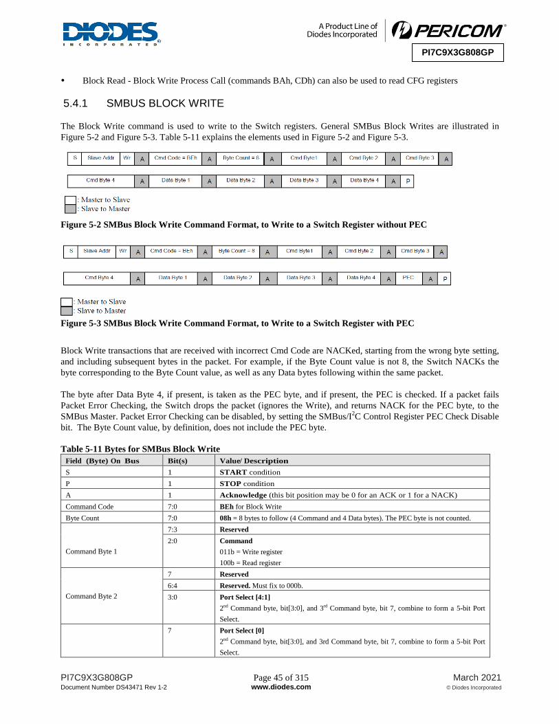
PI7C9X3G808GP Page 45 of 315 March 2021
Document Number DS43471 Rev 1-2 www.diodes.com © Diodes Incorporated
PI7C9X3G808GP
Block Read - Block Write Process Call (commands BAh, CDh) can also be used to read CFG registers
5.4.1 SMBUS BLOCK WRITE
The Block Write command is used to write to the Switch registers. General SMBus Block Writes are illustrated in
Figure 5-2 and Figure 5-3. Table 5-11 explains the elements used in Figure 5-2 and Figure 5-3.
Figure 5-2 SMBus Block Write Command Format, to Write to a Switch Register without PEC
Figure 5-3 SMBus Block Write Command Format, to Write to a Switch Register with PEC
Block Write transactions that are received with incorrect Cmd Code are NACKed, starting from the wrong byte setting,
and including subsequent bytes in the packet. For example, if the Byte Count value is not 8, the Switch NACKs the
byte corresponding to the Byte Count value, as well as any Data bytes following within the same packet.
The byte after Data Byte 4, if present, is taken as the PEC byte, and if present, the PEC is checked. If a packet fails
Packet Error Checking, the Switch drops the packet (ignores the Write), and returns NACK for the PEC byte, to the
SMBus Master. Packet Error Checking can be disabled, by setting the SMBus/I2C Control Register PEC Check Disable
bit. The Byte Count value, by definition, does not include the PEC byte.
Table 5-11 Bytes for SMBus Block Write
Field (Byte) On Bus Bit(s) Value/ Description
S 1 START condition
P 1 STOP condition
A 1 Acknowledge (this bit position may be 0 for an ACK or 1 for a NACK)
Command Code 7:0 BEh for Block Write
Byte Count 7:0 08h = 8 bytes to follow (4 Command and 4 Data bytes). The PEC byte is not counted.
Command Byte 1
7:3 Reserved
2:0 Command
011b = Write register
100b = Read register
Command Byte 2
7 Reserved
6:4 Reserved. Must fix to 000b.
3:0 Port Select [4:1]
2nd Command byte, bit[3:0], and 3rd Command byte, bit 7, combine to form a 5-bit Port
Select.
7 Port Select [0]
2nd Command byte, bit[3:0], and 3rd Command byte, bit 7, combine to form a 5-bit Port
Select.

PI7C9X3G808GP Page 46 of 315 March 2021
Document Number DS43471 Rev 1-2 www.diodes.com © Diodes Incorporated
PI7C9X3G808GP
Field (Byte) On Bus Bit(s) Value/ Description
Command Byte 3
Port Select [4:0] is used to select Port to access.
6 Reserved
5:2 Byte Enable
Bit Description
2 Byte Enable for Data Byte 4 (Switch register bit[7:0])
3 Byte Enable for Data Byte 3 (Switch register bit[15:8])
4 Byte Enable for Data Byte 2 (Switch register bit[23:16])
5 Byte Enable for Data Byte 1 (Switch register bit[31:24])
0 = Corresponding Switch register byte will not be modified
1 = Corresponding Switch register byte will be modified
1:0 Switch Register Address [11:10]
Command Byte 4
7:0 Switch Register Address [9:2]
Note: Address bit[1:0] are fixed to 0.
Data Byte 1 7:0 Data write to register bit[31:24]
Data Byte 2 7:0 Data write to register bit[23:16]
Data Byte 3 7:0 Data write to register bit[15:8]
Data Byte 4 7:0 Data write to register bit[7:0]
PEC 7:0 Packet Error Code
The table below is a sample to write SSID/SSVID register (offset A8h) in Port 1. The register value is 1234_5678h,
with all bytes enabled, and without PEC. The default SMBus Address is 1101000b.
Table 5-12 Sample SMBus Block Write Byte Sequence
Byte Number Byte Type Value Descroption
1 Address D0h Bit[7:1] for the Switch default Slave address of 68h, with bit 0 Cleared to
indicate a Write.
2 Command Code BEh Command Code for register Write, using a Block Write
3 Byte Count 08h Byte Count. Four Command Bytes and Four Data Bytes
4 Command Byte 1 03h For Write command
5 Command Byte 2 00h Bit[6:4] – must fix to 000b
Bit[3:0] - Port Select [4:1] (for Port 1)
6 Command Byte 3 BCh Bit 7 is Port Select[0]
Bit 6 is reserved
Bit[5:2] are the for Byte Enables; all are active
Bit[1:0] are register Address bit[11:10]
7 Command Byte 4 2Ah Switch Register Address bit[9:2] (for offset A8h)
8 Data Byte 1 12h Data Byte for register bit[31:24]
9 Data Byte 2 34h Data Byte for register bit[23:16]
10 Data Byte 3 56h Data Byte for register bit[15:8]
11 Data Byte 4 78h Data Byte for register bit[7:0]
5.4.2 SMBUS BLOCK READ
A Block Read command is used to read Switch CFG registers. Similar to CFG register Reads using I2C, a SMBus
Write sequence must first be performed to select the register to read, followed by a SMBus Read of the corresponding
register. There are two ways a Switch register can be read:
Use a Block Write, followed by a Block Read. The Block Write sets up the parameters including Port Number,
register address and Byte Enables, and the Block Read performs the actual Read operation.

PI7C9X3G808GP Page 47 of 315 March 2021
Document Number DS43471 Rev 1-2 www.diodes.com © Diodes Incorporated
PI7C9X3G808GP
Use a Block Read - Block Write Process Call. This command is defined by the SMBus v2.0, and performs a
Block Write and Block Read, using a single command. The Block Write portion of the message sets up the
register to be read, and then a repeated START followed by the Block Read portion of the message returns the
register data specified by the Block Write
The Switch always NACKs any incorrect command sequences, starting with the wrong Byte. Upon receiving the Block
Read command, the Switch returns a PEC to the Master, if after the 4th byte of register data, the Master still requests
one more Byte. As a Slave, the Switch recognizes the end of the Master's Read cycle, by observing the Master’s NACK
response for the last Data Byte transmitted by the Switch.
Incorrect command sequences are always NACK, starting with the byte that is incorrect. (Refer to Table 5-13.) On the
Block Read command, a PEC is returned to the Master, if after the 4th byte of CSR data, the return Master still requests
for one additional byte. As a Slave, the Switch will know the end of the Master Read cycle, by observing the NACK
for the last byte read from the Master.
Figure 5-4 SMBus Block Write to Set up Read, and Resulting Read that Returns CFG Register Value
Table 5-13 Bytes for SMBus Block Read
Field (Byte) On Bus Bit(s) Value/ Description
S 1 START condition
P 1 STOP condition
A 1 Acknowledge (this bit position may be 0 for an ACK or 1 for a NACK)
Command Code 7:0 BAh, to set up Read, using Block Writes
Byte Count 7:0 04h, 4 Command bytes
Command Byte 1
7:3 Reserved
2:0 Command
011b = Write register
100b = Read register
Command Byte 2
7 Reserved
6:4 Reserved. Must fix to 000b.
3:0 Port Select [4:1]
2nd Command byte, bit[3:0], and 3rd Command byte, bit 7, combine to form a 5-bit Port
Select.
7 Port Select [0]
2nd Command byte, bit[3:0], and 3rd Command byte, bit 7, combine to form a 5-bit Port
Select.
Port Select [4:0] is used to select Port to access.
6 Reserved
5:2 Byte Enable

PI7C9X3G808GP Page 48 of 315 March 2021
Document Number DS43471 Rev 1-2 www.diodes.com © Diodes Incorporated
PI7C9X3G808GP
Field (Byte) On Bus Bit(s) Value/ Description
Command Byte 3
Bit Description
2 Byte Enable for Data Byte 4 (Switch register bit[7:0])
3 Byte Enable for Data Byte 3 (Switch register bit[15:8])
4 Byte Enable for Data Byte 2 (Switch register bit[23:16])
5 Byte Enable for Data Byte 1 (Switch register bit[31:24])
0 = Corresponding Switch register byte will not be modified
1 = Corresponding Switch register byte will be modified
1:0 Switch Register Address [11:10]
Command Byte 4
7:0 Switch Register Address [9:2]
Note: Address bit[1:0] are fixed to 0.
Command Code 7:0 BDh for Block Read
Data Byte 1 7:0 Return value for CFG register bit[31:24]
Data Byte 2 7:0 Return value for CFG register bit[23:16]
Data Byte 3 7:0 Return value for CFG register bit[15:8]
Data Byte 4 7:0 Return value for CFG register bit[7:0]
Table 5-14, Table 5-15, Table 5-16 and Table 5-17 are a sample to Read SSID/SSVID register (offset A8h) in Port 1.
The register value is 0000_0000h, with all bytes enabled, and without PEC. The default SMBus Address is 1101000b.
Table 5-14 SMBus Block Write Portion
Byte Number Byte Type Value Descroption
1 Address D0h Bit[7:1] for the Switch default Slave address of 68h, with bit 0 Cleared to
indicate a Write.
2 Command Code BAh Command Code for register Write, using a Block Write
3 Byte Count 04h Byte Count. Four Command Bytes
4 Command Byte 1 04h For Read command
5 Command Byte 2 00h Bit[6:4] - must fix to 000b
Bit[3:0] - Port Select [4:1] (for Port 1)
6 Command Byte 3 BCh Bit 7 is Port Select[0]
Bit 6 is reserved
Bit[5:2] are the for Byte Enables; all are active
Bit[1:0] are register Address bit[11:10]
7 Command Byte 4 2Ah Switch Register Address bit[9:2] (for offset A8h)
Table 5-15 SMBus Block Read Portion
Byte Number Byte Type Value Description
1 Address D0h Bit[7:1] value for the Switch Slave address of 68h, with bit 0 Cleared to
indicate to indicate a Write.
2 Block Read Command Code BDh Command code for Block Read of Switch registers.
Table 5-16 SMBus Read Command following Repeat START from Master
Byte Number Byte Type Value Description
1 Address D1h Bit[7:1] value for the Switch Slave address of 68h, with bit 0 Set to indicate a
Read.
Table 5-17 SMBus Return Bytes
Byte Number Byte Type Value Description
1 Byte Count 04h Four Bytes in register
2 Data Byte 1 00h Register data [31:24]

PI7C9X3G808GP Page 49 of 315 March 2021
Document Number DS43471 Rev 1-2 www.diodes.com © Diodes Incorporated
PI7C9X3G808GP
Byte Number Byte Type Value Description
3 Data Byte 2 00h Register data [23:16]
4 Data Byte 3 00h Register data [15:8]
5 Data Byte 4 00h Register data [7:0]
Table 5-18 SMBus Return Bytes
Field (Byte) On Bus Bit(s) Value/Description
Command Code 7:0 CDh for Block Read (Process Call Read)
5.4.3 CSR READ, USING SMBUS BLOCK READ – BLOCK WRITE PROCESS CALL
A general SMBus Block Read - Block Write Process Call sequence is illustrated in
Figure 5-5. Alternatively, a general SMBus Block Read - Block Write Process Call with PEC sequence is illustrated in
Figure 5-6.
Using this command, the register to be read can be set up and read back with one SMBus cycle (a transaction with a
START and ending in STOP). There is no STOP condition before the repeated START condition. The command
format for the Block Write part of this command has the same sequence as inTable 5-14, except that the Command
Code changes to CDh, as illustrated below. Other Bytes remain the same as used in the sequence for SMBus Block
Write followed by Block Read. Table 5-18 lists the Command format for Block Read.
Figure 5-5 CSR Read Operation Using SMBus Block Read – Block Write Process Call
Figure 5-6 CSR Read Operation Using SMBus Block Read – Block Write Process Call with PEC
5.5 I2C INTERFACE
Inter-Integrated Circuit (I2C) is a bus used to connect Integrated Circuits (ICs). Multiple ICs can be connected to an I
2C
Bus, and I2C devices that have I
2C mastering capability can initiate a Data transfer. I
2C is used for Data transfers
between ICs at relatively low rates (100 Kbps), and is used in a variety of applications. For further details regarding I2C
Buses, refer to the I2C Bus v2.1.
The Switch is an I2C Slave. Slave operations allow the Switch's Configuration Registers to be read from or written to
by an I2C Master, external from the device. I
2C is a sideband mechanism that allows the device Configuration registers
to be programmed, read from, or written to, independent of the PCI Express upstream Link.

PI7C9X3G808GP Page 50 of 315 March 2021
Document Number DS43471 Rev 1-2 www.diodes.com © Diodes Incorporated
PI7C9X3G808GP
Figure 5-7 Standard Devices to I2C Bus Connection Block Diagram
The I2C interface on the Packet Switch consists of a I
2C clock pin (SCL_I2C), a I
2C data pin (SDA_I2C), and 3 I
2C
address pins (I2C_ADDR[2:0]). The I2C clock pin provides or receives the clock signal. The I
2C data pin facilitates the
data transmission and reception. Both of the clock and data pins are bi-directional. The I2C address pins determine the
address to which the Packet Switch responds to. The I2C address pins generate addresses according to the following
table:
Table 5-19 I2C Address Pin Configuration
BIT I2C Address
0 I2C_ADDR[0]
1 I2C_ADDR[1]
2 I2C_ADDR[2]
3 1
4 0
5 1
6 1
Software can change the I2C Slave address, by programming the SMBus/I
2C Control Register SMBus/I
2C Device
Address field.
5.5.1 I2C REGISTER WRITE ACCESS
The Switch Configuration registers can be read from and written to, based upon I2C register Read and Write operations,
respectively. An I2C Write packet consists of Address Phase bytes and Command Phase bytes, followed by one to four
additional I2C Data bytes. Table 5-20 defines mapping of the I
2C Data bytes to the Configuration register Data bytes.
The I2C packet starts with the S (START condition) bit. Data bytes are separated by the A (Acknowledge Control
Packet (ACK)) or N (Negative Acknowledge (NAK)) bit. The packet ends with the P (STOP condition) bit.
If the Master generates an invalid command, the targeted Switch register is not modified. The Switch considers the 1st
Data byte of the 4-byte Data phase, following the four Command bytes in the Command phase, as register Byte 3
(bit[31:24]). The next three Data bytes access register Bytes 2 through 0, respectively. Four Data bytes are required,
regardless of the Byte Enable Settings in the Command phase. The Master can then generate either a STOP condition
(to finish the transfer) or a repeated START condition (to start a new transfer). If the I2C Master sends more than the
four Data bytes (violating Switch protocol), further details regarding J2C protocol, the Switch returns a NAK for the
extra Data byte(s).

PI7C9X3G808GP Page 51 of 315 March 2021
Document Number DS43471 Rev 1-2 www.diodes.com © Diodes Incorporated
PI7C9X3G808GP
Table 5-21 describes each I2C Command byte for Write access. In the packet described in Figure 5-8, Command Bytes
0 through 3 for Writes follow the format specified in Table 5-21.
Table 5-20 I2C Register Write Access
I2C Data Byte Order PCI Express Configuration Register Byte
0 Written to register Byte 3
1 Written to register Byte 2
2 Written to register Byte 1
3 Written to register Byte 0
Table 5-21 I2C Command Format for Write Access
Byte Bit(s) Description
1st (0) 7:3 Reserved
2:0 Command
011b = Write register
2nd (1) 7 Reserved
6:4 Reserved. Must fix to 000b.
3:0 Port Select [4:1]
2nd Command byte, bit[3:0], and 3rd Command byte, bit 7, combine to form a 5-bit Port Select.
3rd (2) 7 Port Select [0]
2nd Command byte, bit[3:0], and 3rd Command byte, bit 7, combine to form a 5-bit Port Select.
Port Select [4:0] is used to select Port to access.
6 Reserved
5:2 Byte Enable
Bit Description
2 Byte Enable for Data Byte 4 (Switch register bit[7:0])
3 Byte Enable for Data Byte 3 (Switch register bit[15:8])
4 Byte Enable for Data Byte 2 (Switch register bit[23:16])
5 Byte Enable for Data Byte 1 (Switch register bit[31:24])
0 = Corresponding Switch register byte will not be modified
1 = Corresponding Switch register byte will be modified
1:0 Switch Register Address [11:10]
4th (3) 7:0 Switch Register Address [9:2]
Note: Address bit[1:0] are fixed to 0.
Figure 5-8 I2C Write Packet
I2C Write Packet Address Phase Byte
Address Cycle
START 7654321 0 ACK/NAK
S Slave Address [7:1] Read/Write Bit
0 = Write A
I2C Write Packet Command Phase Byte
Command Cycle
76543210 ACK/NAK 76543210 ACK/NAK 76543210 ACK/NAK 76543210 ACK/NAK
Command
Byte 0 A
Command
Byte 1 A
Command
Byte 2 A
Command
Byte 3 A

PI7C9X3G808GP Page 52 of 315 March 2021
Document Number DS43471 Rev 1-2 www.diodes.com © Diodes Incorporated
PI7C9X3G808GP
I2C Write Packet Data Phase Byte
Write Cycle
76543210 ACK/NAK 76543210 ACK/NAK 76543210 ACK/NAK 76543210 ACK/NAK STOP
Register Byte 3 A Register Byte 2 A Register Byte 1 A Register Byte 0 A P
The following tables illustrate a sample I2C packet for writing the Switch SSID/SSVID register (offset A8h) for Port 0,
with data 1234_5678h.
Note: The Switch has a default I2C Slave address [6:0] value of 68h, with the I2C_ADDR[2:0] input having a value of
000. The byte sequence on the I2C Bus, as listed in the following tables, occurs after the START and before the STOP
bits, by which the I2C Master frames the transfer.
Figure 5-9 I2C Register Write Access Example
I2C Register Write Access Example – Address Cycle
Phase Value Description
Address D0h Bit[7:1] for Switch I2C Slave Address (68h) with last bit (bit 0) for Write = 0
I2C Register Write Access Example –
Command Cycle
Byte Value Description
0 03h [7:3] Reserved
[2:0] Command, 011b = Write register
1 00h for Port 0 [7] Reserved
[6:4 ] must fix to 000b
[3:0] Port Select[4:1]
2 3Ch for Port 0 [7] Port Select[0]
[6] Reserved
[5:2] Byte Enable, all active.
[1:0] Switch Register Address, Bit[11:10]
3 2Ah [7:0] Switch Register Address, Bit[9:2]
I2C Register Write Access Example –
Data Cycle
Byte Value Description
0 12h Data to Write for Byte 3
1 34h Data to Write for Byte 2
2 56h Data to Write for Byte 1
3 78h Data to Write for Byte 0
Figure 5-10 I2C Write Command Packet Example
I2C Write Packet Address Phase Bytes
1st Cycle
START 7654321 0 ACK/NAK
S Slave Address 1101_000b Read/Write Bit
0 = Write A
I2C Write Packet Command Phase Bytes
Command Cycle
76543210 ACK/NAK 76543210 ACK/NAK 76543210 ACK/NAK 76543210 ACK/NAK
Command
Byte 0
A Command
Byte 1
A Command
Byte 2
A Command
Byte 3
A

PI7C9X3G808GP Page 53 of 315 March 2021
Document Number DS43471 Rev 1-2 www.diodes.com © Diodes Incorporated
PI7C9X3G808GP
0000_0011b 0000_0000b 0011_1100b 0010_1010b
I2C Write Packet Data Phase Bytes
Write Cycle
76543210 ACK/NAK 76543210 ACK/NAK 76543210 ACK/NAK 76543210 ACK/NAK STOP
Register Byte 3 A Register Byte 2 A Register Byte 1 A Register Byte 0 A P
5.5.2 I2C REGISTER READ ACCESS
When the I2C Master attempts to read a Switch register, two packets are transmitted. The 1
st packet consists of Address
and Command Phase bytes to the Slave. The 2nd
packet consists of Address and Data Phase bytes.
According to the I2C Bus, v2.1, a Read cycle is triggered when the Read/Write bit (bit 0) of the 1
st cycle is Set. The
Command phase reads the requested register content into the internal buffer. When the I2C Read access occurs, the
internal buffer value is transferred on to the I2C Bus, starting from Byte 3 (bit[31: 24]), followed by the subsequent
bytes, with Byte 0 (bit[7:0]) being transferred last. If the I2C Master requests more than four bytes, the Switch re-
transmits the same byte sequence, starting from Byte 3 of the internal buffer.
The 1st and 2
nd I
2C Read packets perform the following functions:
1st packet - Selects the register to read
2nd
packet - Reads the register (sample 2nd
packet provided is for a 7-bit Switch I2C Slave address)
Although two packets gare shown for the I2C Read, the I
2C Master can merge the two packets together into a single
packet, by not generating the STOP at the end of the first packet (Master does not relinquish the bus) and generating
REPEAT START.
Table 5-22 describes each I2C Command byte for Read access. In the packet described in Figure 5-11, command Bytes
0 through 3 for Reads follow the format specified in Table 5-22.
Table 5-22 I2C Command Format for Read Access
Byte Bit(s) Description
1st (0) 7:3 Reserved
2:0 Command
100b = Read register
2nd (1) 7 Reserved
6:4 Reserved. Must fix to 000b.
3:0 Port Select [4:1]
2nd Command byte, bit[3:0], and 3rd Command byte, bit 7, combine to form a 5-bit Port Select.
3rd (2) 7 Port Select [0]
2nd Command byte, bit[3:0], and 3rd Command byte, bit 7, combine to form a 5-bit Port Select.
Port Select [4:0] is used to select Port to access.
6 Reserved
5:2 Byte Enable
Bit Description
2 Byte Enable for Data Byte 4 (Switch register bit[7:0])
3 Byte Enable for Data Byte 3 (Switch register bit[15:8])
4 Byte Enable for Data Byte 2 (Switch register bit[23:16])
5 Byte Enable for Data Byte 1 (Switch register bit[31:24])
0 = Corresponding Switch register byte will not be modified
1 = Corresponding Switch register byte will be modified

PI7C9X3G808GP Page 54 of 315 March 2021
Document Number DS43471 Rev 1-2 www.diodes.com © Diodes Incorporated
PI7C9X3G808GP
Byte Bit(s) Description
1:0 Switch Register Address [11:10]
4th (3) 7:0 Switch Register Address [9:2]
Note: Address bit[1:0] are fixed to 0.
Figure 5-11 I2C Read Command Packet
I2C Read Command Packet Address Phase Byte (1
st Packet)
1st Cycle
START 7654321 0 ACK/NAK
S Slave Address[7:1]
Read/Write Bit
0 = Write A
I2C Read Command Packet Command Phase Byte (1st Packet)
Write Cycle
76543210 ACK/NAK 76543210 ACK/NAK 76543210 ACK/NAK 76543210 ACK/NAK
Command
Byte 0 A
Command
Byte 1 A
Command
Byte 2 A
Command
Byte 3 A
I2C Read Data Packet Address Phase Byte (2
nd Packet)
1st Cycle
START 7654321 0 ACK/NAK
S Slave Address[7:1] Read/Write Bit
1 = Read A
I2C Read Data Packet Data Phase Byte (2
nd Packet)
Write Cycle
76543210 ACK/NAK 76543210 ACK/NAK 76543210 ACK/NAK 76543210 ACK/NAK STOP
Register
Byte 3 A
Register
Byte 2 A
Register
Byte 1 A
Register
Byte 0 A P
The following tables illustrate a sample I2C packet for reading the Switch SSID/SSVID register (offset A8h) for Port 0.
The default value for SSID/SSVID register is 0000_0000h.
Note: The Switch has a default I2C Slave address [6:0] value of 68h, with the I2C_ADDR[2:0] inputs having a value
of 000. The byte sequence on the I2C Bus, as listed in the following tables, occurs after the START and before the STOP
bits, by which the I2C Master frames the transfer.
Figure 5-12 I2C Register Read Access Example
I2C Register Read Access Example – Address Cycle (1
st Packet)
Phase Value Description
Address D0h Bit[7:1] for Switch I2C Slave Address (68h) with last bit (bit 0) for Write = 0
I2C Register Read Access Example – Command Cycle (1
st Packet)
Byte Value Description
0 04h [7:3] Reserved
[2:0] Command , 100b = Read register
1 00h for Port 0 [7] Reserved
[6:4] must fix to 000b
[3:0] Port Select [4:1]
2 3Ch for Port 0 [7] Port Select [0]

PI7C9X3G808GP Page 55 of 315 March 2021
Document Number DS43471 Rev 1-2 www.diodes.com © Diodes Incorporated
PI7C9X3G808GP
Byte Value Description
[6] Reserved
[5:2] Byte Enable, All active.
[1:0] Switch Register Address, Bit[11:10]
3 2Ah [7:0] Switch Register Address, Bit[9:2]
I2C Register Read Access Example – 2
nd Packet
Phase Value Description
Address D1h Bit[7:1] for Switch I2C Slave Address (68h) with last bit (bit 0) for Read = 1
Read 00h Byte 3 of Register Read
00h Byte 2 of Register Read
00h Byte 1 of Register Read
00h Byte 0 of Register Read
Figure 5-13 I2C Read Command Packet
I2C Read Command Packet Address Phase Bytes (1
st Packet)
1st Cycle
START 7654321 0 ACK/NAK
S Slave Address 1101_000b Read/Write Bit
0 = Write A
I2C Read Command Packet Command Phase Bytes (1
st Packet)
Command Cycle
76543210 ACK/NAK 76543210 ACK/NAK 76543210 ACK/NAK 76543210
Command
Byte 0
0000_0100b
A
Command
Byte 1
0000_0000b
A
Command
Byte 2
0011_1100b
A
Command
Byte 3
0010_1010b
I2C Read Data Packet Address Phase Bytes (2
nd Packet)
1st Cycle
START 7654321 0 ACK/NAK
S Slave Address [7:1] 1101_000b Read/Write Bit
1 = Read A
I2C Read Data Packet Data Phase Bytes (2
nd Packet)
Command Cycle
76543210 ACK/NAK 76543210 ACK/NAK 76543210 ACK/NAK 76543210 Stop
Register Byte3
0000_0000b A
Register Byte2
0000_0000b A
Register Byte1
0000_0000b A
Register Byte0
0000_00000b P

PI7C9X3G808GP Page 56 of 315 March 2021
Document Number DS43471 Rev 1-2 www.diodes.com © Diodes Incorporated
PI7C9X3G808GP
6 HOT PLUG SUPPORT The hot plug usages can be classified into surprised and managed types depending on the application scenario. Each
type has two different control and status interfaces: serial and parallel. The switch implements both surprised/managed
and serial/parallel hot-plug types in the downstream ports. The HOT_PLUG_EN strap pin should be set to “1” to
enable hot plug function in the downstream ports of the switch.
6.1 HOT PLUG TYPES
6.1.1 SURPRISED SERIAL HOT PLUG
If the device is inserted or removed asynchronously from downstream port, it is called surprised hot plug. When
HOT_PLUG_TYPE strap pin is set to “1”, the chip is operating under surprised hot plug mode.
Hot Insertion Procedures:
Present Detect Pin (i.e. PDC_L[7:0]) is asserted
The corresponding “Presence Detect Change” and “Present Detect State” in slot status reflect the card is in the
slot
Enable the corresponding reference clock output (i.e. REFCLKOP/N[7:0]) to the hot inserted device
Issue INTx Message or MSI to notify software processing hot plug event
Wait for 100ms and then deassert the corresponding downstream reset (i.e. HP_RST_L[7:0]) If DL_UP is set, then generating INTx Message or MSI to notify software initiating configuration cycles to the
hot inserted device
Hot Removal Procedures
The device is removed asynchronously or under abnormal condition (Ex. Human Error …)
Either in-band or out-band Present Detect sensing device being removed
Commands LTSSM state machine to Detect.Quiet state
Upstream port replies UR status that any TLP being sent to this downstream port
Any packet stored in input queue of upstream port will be dropped silently
Assert Present detect change Interrupt to system software
Enable DPC trigger event and assert DPC interrupt and unmasked non-fatal message to system software
Turn off the corresponding output clock buffer and assert the corresponding hot plug reset signal
During power-up, the chip scans IO Expander like devices through I2C clock and data signals (i.e. SHCL_I2C and
SHDA_I2C). According to the reference design described in LED management, one set of I2C bus serves 4 CPLD,
which converts the serial bus into 8-bit parallel bus. The 8-bit mapping is defined in Table 6-1.
Table 6-1 CPLD Signal Name Mapping for 8-bit IO Expander
BIT DIRECTION CPLD SIGNAL NAME
0 O FAULT
1 O LOCATE
2 N/A Not used (Debug Only)
3 N/A Not used (Debug Only)
4 I PRSNT
5 N/A Not used (Debug Only)
6 N/A Not used (Debug Only)
7 N/A Not used (Debug Only)

PI7C9X3G808GP Page 57 of 315 March 2021
Document Number DS43471 Rev 1-2 www.diodes.com © Diodes Incorporated
PI7C9X3G808GP
Among these signals, ATNLED and PWRLED defined in PCIe specification are repurposed to represent FAULT and
LOCATE to be compliant with SFF-8489 for blinking LEDs. For details, please refer to LED Management
specification.
The switch hot plug controller supports multiple I2C/SMBUS-like control interfaces. Each interface can serve up to 8
downstream ports. The I2C/SMBUS address for slave devices is started from 40h by default. In addition, this initial
address is configurable through EEPROM to LTSSM 2 Register, Bit[30] and LTSSM 3 Register, Bit[6:0]. Each
downstream port is correspondent to one equivalent 8-bit IO expander with the following Port/Address mapping table.
Table 6-2 Port/Address Mapping for 8-bit IO Expander
Downstream Port
Number P1 P2 P3 P4 P5 P6 P7 P8
Address 40h 41h 42h 43h 44h 45h 46h 47h
6.1.2 SURPRISED PARALLEL HOT PLUG
The parallel mode of Surprised Hot Plug is very similar to its serial mode except that no CPLD is required to control
LED. Instead, the chip outputs LED signals (i.e. HP_LED [7:0]) to drive Amber LED directly and the blinking follows
SFF-8489 IBPI specification.
6.1.3 MANAGED SERIAL HOT PLUG
If the device is inserted or removed synchronously with hot-plug management software from downstream port, it is
called managed hot plug. When HOT_PLUG_TYPE strap pin is set to “0”, the chip is operating under managed hot
plug mode.
Hot Insertion Procedures: User inserts card
User closes MRL
User initiates hot-inserted sequence by pressing Attention Button
System commands slot control register to drive indicators and power on slot
System starts re-enumeration the hierarchy under the slot
Hot Removal Procedures: User initiates hot-removed sequence by pressing Attention Button
System informs application/driver to complete current task
System commands slot control register to drive indicators and power off slot
System disabled the hierarchy under the slot
User opens MRL and removes the card
During the process of hot insertion and removal, there are hot plug events corresponding to slot status bits ready for
generation. When Hot-Plug Interrupt Enable bit is set, either MSI or INT message is issued to notify S/W for
processing.
When power-up, the chip uses I2C clock and data signals to scan either 16-bit or 40-bit IO Expander dependent on the
setting of LTSSM 2 REGISTER – OFFSET 398h. The IO Expander responds an interrupt (i.e. SHPCINT_L) to notify
any hot plug signal status change and the chip will read back the status change in serial mode and reflect on slot status
register. The 16-bit mapping of managed hot plug events for I2C bit sequence is defined in Table 6-3

PI7C9X3G808GP Page 58 of 315 March 2021
Document Number DS43471 Rev 1-2 www.diodes.com © Diodes Incorporated
PI7C9X3G808GP
Table 6-3 CPLD Signal Name Mapping for 16-bit IO Expander
BIT DIRECTION CPLD SIGNAL NAME
0 O PWRLED
1 O ATNLED
2 O PWREN
3 O RECLKEN
4 O PERST
5 O INTERLOCK
6 N/A N/A
7 I SLOT#[0]
8 I SLOT#[1]
9 I SLOT#[2]
10 I SLOT#[3]
11 I PRSNT
12 I MRL
13 I ATNBTN
14 I PWRFLT
15 I PWRGOOD
Similar to Surprised Serial Hot Plug, each downstream port is correspondent to one equivalent 16-bit IO expander with
the following Port/Address mapping table.
Table 6-4 Port/Address Mapping for 16-bit IO Expander
Downstream Port
Number P1 P2 P3 P4 P5 P6 P7 P8
Address 40h 42h 44h 46h 48h 4Ah 4Ch 4Eh
6.2 TIMING SEQUENCE FOR SURPRISED HOT PLUG OPERATION
Two timing charts are shown below to illustrate surprised hot insertion or removal under different scenarios. The first
chart presents the timing relationship between system reset/reference_clock and individual downstream
reset/reference_clock under initial power-up condition. The second chart demonstrates the timing sequence of clock
and reset for device inserted or removed under power active condition.

PI7C9X3G808GP Page 59 of 315 March 2021
Document Number DS43471 Rev 1-2 www.diodes.com © Diodes Incorporated
PI7C9X3G808GP
Note: There is a device in slot#0 while slot#15 is empty.
Figure 6-1 Timing Sequence for Surprised Hot Plug Operation

PI7C9X3G808GP Page 60 of 315 March 2021
Document Number DS43471 Rev 1-2 www.diodes.com © Diodes Incorporated
PI7C9X3G808GP
7 CROSS-DOMAIN END-POINT
7.1 GENERAL DESCRIPTION
The PCIe Packet Switch supports Cross-Domain End-Point (CDEP) function. The function, when working in
conjunction with the software running on the PRIMARY HOST, enables data exchange among multiple PCIe-based
hosts. This feature allows the system to implement fail-over or co-processor functionalities. These two use cases are
briefly described in the following sections with the suitable CDEP Mode Switch Model for the use case.
7.1.1 FAIL-OVER
In an error resilient system, a back-up or secondary host is set up to take over the primary host in the event when
primary has failed and the failure is detected. The CDEP Mode Switch Model facilitates the data exchange across
domains of the primary and secondary hosts, and swaps the roles of the hosts in the event of the primary host's failure.
The CDEP Mode Switch Model used in the fail-over use case is shown in the illustration below.
Figure 7-1 Switch Reference Model Used in the Fail-Over Use Case
In the event when the primary host is unable to send regular messages to the back-up host, the back-up host can swap
its role to the primary host and its CDLEP port being a agent of upstream port to handle the traffic to/from downstream
ports. . The previous primary host's upstream port will be reset during the link-down process initiated by the previous
primary host. The Switch has to ensure that the reset does not propagate to the entire upstream hierarchy in the
previous primary host's, so that the new primary host can seamlessly manage the original End-Points. As a result, the
impacts to the entire system are minimal during the fail-over transition.
7.1.2 CO-PROCESSOR
The co-processor can be connected to the CDLEP port to off-load the computation on the primary host. The illustration
below shows a co-processor unit (CP), which works with the Primary Host to form a two-processor system. The DMA
function of the PRIMARY HOST's upstream port is enabled to move data among the Primary Host and co-processor to
accelerate intensive computation tasks.

PI7C9X3G808GP Page 61 of 315 March 2021
Document Number DS43471 Rev 1-2 www.diodes.com © Diodes Incorporated
PI7C9X3G808GP
Figure 7-2 Switch Reference Model Used in the Co-Processor Use Case
7.2 PORT CONFIGURATION
The Primary Host can configure a link CDEP port as a generic PCIe End-Point. This allows the secondary host(s) the
ability to link to the switch CDEP port during PCIe enumeration. The enumeration process includes BIOS start-up,
operating system start-up, and/or subsequent PCIe hot-plug or dynamic enumerations initiated by the host operating
system
Before the Primary Host can enable the CDEP function, the Switch has to be configured into the CDEP mode and
designate the CDEP port to as the upstream port of a generic end-point. The configuration is performed through
EEPROM programming at power-up. In order to operate in the CDEP mode, the Switch is required to set Chip CD
Mode and Switch CD Mode for the CDEP port configurations. The Chip CD Mode and Switch CD Mode are defined
in the Device Configuration 0 and 2 Registers respectively.
In order to support the CDEP mode, the Switch has to contain a Cross-Domain Virtual End-Point (CDVEP). The
CDVEP acts as an agent to bridge the PRIMARY HOST and other host domain, and only exists in the Switch.
In addition to the CDVEP, the Switch has another type of End-Point, called Cross-Domain Line End-Point (CDLEP).
The CDLEP is visible to the Local Host (LH), but not the PRIMARY HOST. The CDLEP bridges the communications
between the LH and other HOST. The table below describes the CDEP port's configurations by the Switch types.
Table 7-1 CDEP Mode Configuration
Switch CD Mode CDEP Configuration
0x Both CDEPs disabled
10 Illeagal Configuration
11 CDVEP enabled, and CDLEP enabled
Only P4 can be designated as a CDLEP port. Once the port is chosen as CDLEP port, the port number defined in Link
Capability Register and MMIO Register offsets will be changed accordingly. Please refer to the application note of
CDEP operation for more information.
7.3 BAR TRANSLATION FOR LOCAL HOST DOMAIN
The PRIMARY HOST configures a set of CDEP Link address translations to the Switch. The translations allow the
Local Host to access the CDEP Link’s 64-bit BAR2/BAR3 and BAR4/BAR5 similar to accessing the other HOST
locations. The PRIMARY HOST software is responsible for managing the memory regions appropriately to implement
and emulate the CDLEP end-point behaviors.
The PRIMARY HOST defines either or both of a Direct Address Translation (DAT) range, and an Address Look-up
Table (ALUT) for the BAR translations for the LH to access to other HOST memory locations. The PRIMARY HOST

PI7C9X3G808GP Page 62 of 315 March 2021
Document Number DS43471 Rev 1-2 www.diodes.com © Diodes Incorporated
PI7C9X3G808GP
configures these settings prior to enabling the CDLEP port. After the PRIMARY HOST programs the CDLEP port’s
BARs, the LH is able to read/write to the PRIMARY HOST or other LH memory locations.
7.3.1 DIRECT ADDRESS TRANSLATION (DAT)
The PRIMARY HOST arranges a contiguous memory block in the LH domain by setting BAR Configuration registers
with the chosen DAT. The BAR2/BAR3 and BAR4/BAR5 have their own corresponding contiguous memory blocks.
These memory blocks are characterized by the Base bits and Window Size bits. If the upper address of incoming TLP
matches with the Base bits, the upper address will be replaced with the translated address stored in Base Translation
Registers (BTR2/BTR3 and BTR4/BTR5). The lower address bits are defined by the Window Size bits and remain
intact. They are considered to be an offset address from the base address. The Window Size is determined by the BAR
configuration, and the minimum size is 1MB.
7.3.2 ADDRESS LOOK-UP TRANSLATION (ALUT)
In addition to the Direct Address Translation, the BAR2/BAR3 provides an alternative address translation mechanism,
Address Look-Up Translation (ALUT). The ALUT allows multiple translated address blocks in a non-contiguous
address range. The Window Size bits defined earlier can be partitioned into 7 index bits and the rest lower address bits
can form Page Size bits. The minimum page size is 8KB (1MB divided by 128). The 7 index bits are used to access
128 entries. Each entry represents a translated address block and the host domain destination it is associated with.
The ALUT Access Control Registers at offset from 918h to 920h in the CDLEP is used to store 128 entries. When
performing ALUT entry write, the software has to program the ALUT data into the CDLEP at offset 91Ch and 920h if
the translated address is 64-bit. The software then updates the index and Command (set to write) fields of the CDLEP
at offset 918h. When performing LUT entry read, the software has to program index and Command (set to read) fields
of the CDLEP at offset 918h, and then read 91Ch and 920h to get the LUT data.
7.3.3 ID TRANSLATION
In the event when a PCIe read or write is initiated in the LH PCIe domain, and the read/write targets the PRIMARY
HOST memory or an end-point in the PRIMARY HOST PCIe domain, the PCIe Requestor ID field in the TLP header
that targets the PRIMARY HOST must be translated into the PCIe Requestor ID of the CDVEP. This is to ensure that
the IOMMU access permissions granted by the MPCU operating system, virtual machine, and/or end-point driver,
apply to these translated TLPs. If the target is to another LH PCIe domain, the PCIe Requestor ID has to be translated
into the PCIe Requestor ID of the destination CDLEP to ensure that a legal ID is used by the destination LH system.
7.4 BAR TRANSLATION FOR PRIMARY HOST DOMAIN
The PRIMARY HOST also configures a set of CDEP Virtual address translations. The address translations allow
accesses to a defined address range to be translated to the LH memory addresses.
Similar to BAR Translation on the LH domain described previously, the BAR Translation on the PRIMARY HOST
domain also supports two different approaches: the Direct Address Translation and the Address Look-Up table
Translation. Please refer to the section of CDVEP Configuration Register for related BAR translation setup registers
such as BAR Configuration, BTR, ALUT Access Control, and more.
The RID translation in PRIMARY HOST domain is the same as the translation in the LH domain. The only difference
is in building the RID LUT. However, the RID table is programmed by the PRIMARY HOST in the default setting, not
by hardware automatically.

PI7C9X3G808GP Page 63 of 315 March 2021
Document Number DS43471 Rev 1-2 www.diodes.com © Diodes Incorporated
PI7C9X3G808GP
7.5 SCRATCHPADS AND DOORBELLS
The CDEP Link and virtual interfaces may provide a set of switch-specific scratchpad and doorbell registers for uses in
Host-to-PRIMARY HOST/Host communication. By definition, custom driver or diagnostic code is required to run on
the hosts. As a result, the PRIMARY HOST or Local Host must determine their visibility when a CDEP port emulates
a generic End-Point. The registers must appear in PCIe configuration space in user-defined regions.
If the PRIMARY HOST intends to make the scratchpad and doorbell registers visible to the host, the PRIMARY
HOST should define a CDEP Link property that enables a non-prefetchable 32-bit BAR0 containing these scratchpad
and doorbell registers. A 4K range is allocated for CDLEP within the BAR0 at an offset address defined in the table in
section 9.2.3 of the register reference document
In each CDLEP or CDVEP, there are 8 sets of 32-bit scratchpad registers (CDLEP at offset 9E4h~A00h, and CDVEP
at offset 9E4h~A00h), and one set of 32-bit doorbell registers (CDLEP offset 9C4h~9D0h and CDVEP offset
9C4h~9D0h). The scratchpad registers are used to store information for communication among Local Hosts and
PRIMARY HOST. The doorbell registers are utilized to process (set/clear/mask/unmask) interrupt in order to notify
the destination host to fetch the data stored in scratchpad registers of the source host. The scratchpad registers can only
be written by the host in same domain while doorbell registers can be set/clear by both of hosts either in the same
domain or in different domain. If the PRIMARY HOST uses the PCIe configuration command to access scratchpad
and doorbell registers, it keep track of its End-Point-defined region and restrict its range so it does not go over the
offset 9C4h. If the memory commands are used to access these registers in the CDLEP, the PRIMARY HOST has to
enable a non-prefetchable 32-bit BAR3. A 4K range is allocated for CDLEP within the BAR0/1 at an offset address
defined in the address table of Device Specific Memory Mapped Configuration Mechanism.

PI7C9X3G808GP Page 64 of 315 March 2021
Document Number DS43471 Rev 1-2 www.diodes.com © Diodes Incorporated
PI7C9X3G808GP
8 DIRECT MEMORY ACCESS
8.1 GENERAL DESCRIPTION
The Switch provides two DMA engines. These are hardware blocks that includes a set of buffers to asynchronously
read and write to I/O memory through the Switch's ports. Each DMA engine is configured through a corresponding
PCIe Function, managed by a software device driver running on a connected Local Host (LH) or Main Host (MH).
The DMA engine is divided into single or multiple physical channels (2 per engine), providing a reserved portion of
the buffer pool, and access to a set of virtual channels (2 per physical channel). The virtual channels allow the software
initiator to submit lock-free requests, or partition access to the channel among a set of cooperating software subsystems.
The initiator accesses the DMA engine using a physical/virtual channel (hereafter abbreviated as channel) to submit
descriptors. Each descriptor tells the engine to read from a DMA source into one of the channel’s internal buffers, and
then performs a corresponding write to a DMA destination.
The Switch's DMA engines can be configured in a variety of ways, including:
Device Status Collection: A host CPU can off-load blocking MMIO reads of device status registers to the DMA
engine for asynchronous processing.
Peer-to-Peer EP Transfer: A host CPU can off-load memory copies between a set of managed devices in the
Switch.
Peer-to-Peer LH Transfer: A set of cooperating LHs connected through a pair of CDEP ports can use the DMA
Engine as a LH-to-LH memory transport, implementing a message queue.
In this section, any description of register layouts and data formats uses little-endian ordering.
8.2 DMA CONFIGURATION
The Switch's EEPROM or a micro-controller connected via I2C interface first configures the Switch's DMA engines
(functions), enabling the DMA functions to appear underneath appropriate ports. Then, the software attaches a DMA
driver to the DMA function based on the software model for the switch deployment to initialize and manage the set of
channels (descriptor queues), start/stop/restart the channels, and perform appropriate error handling.
8.2.1 DMA FUNCTIONS
The Switch's EEPROM and switch configuration registers are set to indicate the ports under which the DMA functions
will be visible to the connected LH or MH. This may include upstream ports, CDEP Link Ports, or virtual upstream
ports.
The Device Configuration 2 Register (offset 50Ch) defined in upstream port (Port 0) is used to configure DMA
function (bit[19:18]) under various CD modes (bit[17:16]) (Please refer to CDEP Chapter for CD mode definition).
The DMA mode definition is represented by the following table.

PI7C9X3G808GP Page 65 of 315 March 2021
Document Number DS43471 Rev 1-2 www.diodes.com © Diodes Incorporated
PI7C9X3G808GP
Table 8-1 DMA Mode definition
DMA Mode DMA Configuration
0x DMA functions disabled
10 DMA functions enabled for P0 or P4 based upon CD mode
11 DMA functions enabled for P0 only
8.2.1.1 DMA MODE BIT DEFINITION
Bit #1: Decides if DMA function is enabled in the port connected to LH or MH.
0: DMA function is disabled
1: DMA function is enabled
Bit #0: Determines if DMA function only visible to the MH's domain
0: DMA function is visible to its own local host or the MH's domain
1: DMA function is only visible to the MH's domain
8.2.1.2 DMA MODE AND CD MODE
DMA function is defined in the various ports under different CD and DMA mode settings. These ports are respectively
“P0 port” and “CDLEP port”. A comprehensive table as shown below illustrates how the DMA functions (F1 or F2)
being assigned to these three types of ports in terms ofCD and DMA modes.
Table 8-2 DMA Function Definition in P0 and CDLEP Under Various Modes
CD Mode DMA Mode P0/F0 P0/F1/F2 P4/F0 P4/F1
00 00 Up-Port N/A Down-Port N/A
00 01 Up-Port N/A Down-Port N/A
00 10 Up-Port 2 DMAs Down-Port N/A
00 11 Up-Port 2 DMAs Down-Port N/A
01 00 Up-Port N/A Down-Port N/A
01 01 Up-Port N/A Down-Port N/A
01 10 Up-Port 2 DMAs Down-Port N/A
01 11 Up-Port 2 DMAs Down-Port N/A
11 00 Up-Port* N/A CDLEP N/A
11 01 Up-Port* N/A CDLEP N/A
11 10 Up-Port* 1 DMA CDLEP 1 DMA
11 11 Up-Port* 2 DMAs CDLEP N/A
Note: Up-Port* means that CDVEP exists in the Up-Port host domain
8.2.1.3 ENUMERATION
The PCIe configuration space for each port that has been configured for DMA will enumerate one or more DMA
Functions (Type0 configuration space headers), with a well-defined vendor, device, and class code indicating DMA,
and a set of control registers associated with a non-prefetchable BAR. Software will enumerate each DMA Function
and program BARs. These configuration registers for function #1 or function #2 is defined in the chapter 9 of this
document.
8.2.2 DMA CONTROL REGISTER
DMA engine (i.e. function) provides a set of interface registers for software to control the operation and monitor the
status of DMA transfer for all channels managed by this function. These registers are accessed by mmio via a base
address defined in non-prefetchable BAR0 and BAR1 registers associated with the channel and individual register

PI7C9X3G808GP Page 66 of 315 March 2021
Document Number DS43471 Rev 1-2 www.diodes.com © Diodes Incorporated
PI7C9X3G808GP
offset defined in the section 5 of this document. For each channel, it will add an additional 100h offset to indicate the
interface registers of one channel located in a 256-byte block. Hence, the access to one particular interface register in
one of channels requires to set the address offset as follows: register offset + (number of channel) x 100h. Software can
check the Channel ID field (Bit 31:28) of DMA Control and Status Register 0 at offset 00h to see if it is accessing the
desired channel.
8.2.2.1 DMA DESCRIPTOR REGISTER
The DMA control register space will include a 64-bit pointer to the i/o address base of each channel’s descriptor ring,
and the size of the descriptor ring. Software will program the DMA registers to configure each descriptor ring, from
which a channel will prefetch. The channel will support a total size for each descriptor ring of at most 4096 entries.
8.2.2.1.1 DESCRIPTOR POINTER REGISTER
The I/O address base of each channel’s descriptor ring is pointed by a 64-bit channel descriptor ring base pointer at
register offset 0Ch and 10h. The software has to program these registers, so the hardware can prefetch the descriptors
starting from there.
8.2.2.1.2 DESCRIPTOR SIZE REGISTER
The size of descriptor ring can be programmed in register offset 24h (Bit 12:0 in Channel Descriptor Ring Size for
Prefetch register). The maximum descriptor ring size is 4096 entries. The Bit 28:16 of this register indicates the next
descriptor index is going to be prefetched.
8.2.2.2 DMA OPERATIONAL REGISTER
The DMA control register space will include a control register (DMA Control and Status Register 1 at register offset
20h) for each channel to start, stop, abort, pause, and resume DMA activity for the channel. Software will update the
control register to start the engine once it is ready to begin submitting requests. Software will update the control
register if it needs to pause, stop, or otherwise reconfigure a channel.
After starting the DMA activity for that virtual channel (i.e. write “1” to Bit 0 of DMA Control and Status Register 1),
the software can update the control register any time by commanding the DMA engine to pause, abort or stop operation.
Following is a summary for these three operations.
8.2.2.2.1 PAUSE (BIT 1)
When set, the DMA activity is paused to the next active descriptor after completing the processing on current
descriptor. Then, the DMA Pause Done status (Bit 16) is turned on to represent the DMA is in “paused” condition. If
DMA Pause Interrupt Enable (Bit 3) is set, an interrupt will be issued to notify the software when Bit 16 is set. For
pause operation, there is no any descriptor or data being dropped and the DMA operation can be resumed any time by
clearing the Pause Control (Bit 1).
8.2.2.2.2 ABORT (BIT 2)
When set, the DMA activity drops the current active descriptor by flushing out all outstanding read commands and
discarding all received completion data. The pointer will move to the next active descriptor. Then, the DMA Abort
Done status (Bit 17) is turned on to represent the DMA is in “aborted” condition. If DMA Abort Interrupt Enable (Bit 6)
is set, an interrupt will be issued to notify the software when Bit 17 is set. In abort condition, the DMA operation can
be resumed any time by clearing the Abort Control (Bit 2) and setting DMA Start (Bit 0). Then, DMA begins to
process the next active descriptor. In fact, the software is also allowed to reprogram interface registers for re-
initialization and start from the base descriptor pointer.
8.2.2.2.3 STOP (BIT 7)
When set, the DMA activity drops the current active descriptor by flushing out all outstanding read commands and
discarding all received completion data. The channel interface registers are all cleaned to default state except Interrupt
flag bit if DMA stop enable is set earlier. Then, the DMA Stop Done status (Bit 18) is turned on to represent the DMA
is in “stopped” condition. If DMA Stop Interrupt Enable (Bit 5) is set, an interrupt will be issued to notify the software

PI7C9X3G808GP Page 67 of 315 March 2021
Document Number DS43471 Rev 1-2 www.diodes.com © Diodes Incorporated
PI7C9X3G808GP
when Bit 18 is set. In stop condition, the data buffer contents pointed by the previous processed descriptor will be
dropped as well, so the software needs to reprogram interface registers for re-initialization before resuming DMA
activity by setting DMA Start (Bit 0).
8.3 DMA DESCRIPTORS AND TRANSFERS
Each DMA channel will initiate descriptor pre-fetch when the channel is enabled and its ownership register is updated,
indicating the valid range of descriptors to prefetch. When a valid descriptor is found, a DMA transfer will be
scheduled with the underlying DMA engine in a fair manner with respect to other descriptors from other channels. The
descriptor will be re-written by the DMA engine when the DMA transfer is complete, or if the DMA transfer fails due
to an error. The switch will also update the ownership register to indicate the range of completed descriptors.
Software will then examine the completed descriptors and take appropriate action.
8.3.1 DESCRIPTORS
Descriptors are located in the system memory. All of descriptors in a ring have to be concatenated together without gap
(see figure 1. below). The switch will calculate the address offset automatically by adding the index of descriptor
multiplied with the byte count of a single-descriptor to the ring base descriptor pointer for prefetch.
Figure 8-1 DMA Descriptor Map
8.3.1.1 INITIALIZATION
Software will initialize a valid descriptor by writing it to memory at the next free location in a channel’s descriptor ring.
Software will ensure that the descriptor’s valid bit is written only after all other descriptor fields have been initialized.
Software will update the ownership register to schedule execution of all initialized descriptors with the DMA engine.
8.3.1.2 OWNERSHIP
After all descriptor fields have been initialized, Software will update the ownership registers located at the register
offset 04h and 08h by setting valid status. The descriptor ownership 0 register (04h) represents the first 32 descriptors’
valid status starting from bit 0 while the descriptor ownership 1 register (08h) stands for the next 32 descriptors’ valid
status. The switch will pre-fetch the descriptors with valid status turned on continuously until the descriptor with valid
status being cleared. After the descriptors have been processed, the switch will update the ownership registers by
clearing valid status in the order it was received.

PI7C9X3G808GP Page 68 of 315 March 2021
Document Number DS43471 Rev 1-2 www.diodes.com © Diodes Incorporated
PI7C9X3G808GP
8.3.1.3 PRE-FETCH
Software needs to update the Channel Descriptor Ring Size for Pre-fetch register at offset 24h by writing total
descriptor numbers into Bit 12:0. Starting from the 1st descriptor pointed by ring base pointer register (0Ch and 10h),
the descriptors will be pre-fetched by the switch continuously. The Channel Descriptor Current Pointer register at
offset 14h indicates which descriptor is under processing. The switch will also take a residual function over the
descriptor numbers divided by 64. If the remainder is less than or equal to 64, the switch will go back to prefetch the
1st descriptor after hitting the last descriptor.
When Software prepares to update the ownership registers during the DMA operation, it requires to check Descriptor
current pointer (14h) viewed by the switch in order to update the correct 64-bit sliding window, which is advanced in
terms of descriptor units.
8.3.2 TRANSFER
Software will define in the descriptor a 64-bit i/o source address, 64-bit i/o destination address, and transfer length up
to 8MB. Switch will divide the DMA transfer into appropriate pairs of Memory Read and Write TLPs based on the
current switch settings for Max_Payload_Size and Max_Read_Request_Size, along with any 4k boundaries crossed by
the range of addresses. Other than 64-bit i/o source and 64-bit i/o destination address, Software will also define 4-bit
source domain and 4-bit destination domain in the descriptor for moving data across domains. Switch needs to generate
Read or Write TLPs with a translated RID if the TLP destined domain is different from the domain where the DMA
function is located.
8.3.2.1 LOCAL DOMAIN TRANSFER
For a local DMA transfer (i.e. no crossing host domains, the SDV and DDV must be “0” in the CTRL word of
descriptors), the switch will refer to Max_Payload_Size and Max_Read_Request_Size defined in PCIe configuration
space in where the DMA function is resided for generating MRD and MWR TPLs along with any 4k boundaries
crossed by the range of addresses.
8.3.2.2 CROSS DOMAIN TRANSFER
As to a cross-host-domain DMA transfer (i.e. either SDV or DDV or both are “0”), the switch will refer to
Max_Payload_Size and Max_Read_Request_Size of other host domains defined in register offset 28h, 2Ch and 30h,
which are usually programmed by Main Host. The switch will check the domain number carried in descriptor to choose
the appropriate Max_Payload_Size and Max_Read_Request_Size for creating MRD and MWR TLPs. Please note that
the Main Host software has to program the correct values of Max_Payload_Size and Max_Read_Request_Size for each
domain by following the definition in PCIe configuration device control registers of that domain. Otherwise, it will
cause undesired result in packet transfers.
As the DMA transfer source domain is different from destination domain, the Requester ID needs to be translated into
a legal BDF ID of the destination domain. The software is required to program the captured bus number of CDV or
CDL into domain bus number defined in register offset 34h, 38h and 3Ch. Regarding the captured bus number, the
software can refer to CDEP data 0 register at offset A04h of CD port. The switch will check the domain number
carried in descriptor to choose the appropriate bus number for creating RID of MRD and MWR TLPs.
8.3.3 DESCRIPTOR LAYOUT
The descriptor is formed by an 8-DW data block. The Figure 2 (see below) presents the layout of these DWs containing
control word, source domain/address, destination domain/address, transfer byte count and others.

PI7C9X3G808GP Page 69 of 315 March 2021
Document Number DS43471 Rev 1-2 www.diodes.com © Diodes Incorporated
PI7C9X3G808GP
Figure 8-2 DMA Descriptor Layout in an 8-DW block
8.3.3.1 DOMAIN AND ADDRESS FIELD
The 64-bit I/O destination address and source address are located from the 3rd DW to 6th DW. They must be D-Word
aligned. Also in the 7th DW, it defines the destination domain number (Bit 7 ~ Bit 0) and source domain number (Bit
15 ~ Bit 8) used for cross-domain DMA operation. Each domain number is expressed by LSB 4-bit that represents for
12 different host domain (0 ~ 11) supported by one packet switch. As to MSB 4-bit, they are reserved for future use.
8.3.3.2 TRANSFER COUNT FIELD
The bit 22 ~ bit 0 in the 2nd DW stands for the transfer byte count for one descriptor can be up to 8MB.
8.3.3.3 CONTROL FILED
There are several bits defined in CTRL field of 1st DW for further formatting and enabling the source and destination
locations. Please see Table 3 for illustrating bit definition in CTRL filed.
Table 8-3 Bit Definition in CTRL Field of the 1st DW
Bit Name Description
31 EOT End of transfer
30 INT Issue interrupt when DMA done
29 TPH TPH function enable
28 NOP No operation
27 FLH Dlush any cached data
26 SAV Source address is valid
25 DAV Destination address is valid
24 64bit Rnable 64 bit address
23 SAV Source domain is valid
22 DDV Destination domain is valid
21 CRC Enable CRC checksum
EOT(End of Transfer): Defined in bit-31. When set, it indicates the current DMA transfer is completed. The
interpretation on EOT is various for different DMA modes.
DMA mode bit#0 = 0: DMA processing is transferred from a source host domain to a destination host domain.
In this condition, EOT bit will be set by software in the source descriptor when it is the last transfer. Once
the destination DMA is notified by this event, the switch will set EOT bit in the destination descriptor and
the transfer byte count will be updated as well. So the destination host would know the last transfer
happening in this descriptor.
DMA mode bit#0 = 1: DMA processing is handled by the root host only. If the EOT valid bit defined in the
DMA control register 0 is set, the switch will update the EOT bit in descriptor from 0 to 1 after transfer
count indicated in descriptor is ended.

PI7C9X3G808GP Page 70 of 315 March 2021
Document Number DS43471 Rev 1-2 www.diodes.com © Diodes Incorporated
PI7C9X3G808GP
64bit: Defined in bit-24. When set, the I/O address is in 64-bit physical memory. Otherwise, it is in 32-bit
physical memory.
SAV: Defined in bit-26. When set, it means the I/O source address is valid. If cleared, the I/O source address is
not valid, which is the condition that only destination DMA channel is enabled for executing host to host DMA.
DAV: Defined in bit-25. When set, it means the I/O destination address is valid. If cleared, the I/O destination
address is not valid, which is the condition that only source DMA channel is enabled for executing host to host
DMA.
SDV: Defined in bit-23. When set, it means the source domain number is valid and MRD will be issued to that
domain by following its max payload size and read request size. It implies that DMA source and DMA function
(or descriptors) are located in different domains. If cleared, it might be in the condition of either only DMA
destination is positioned in a different domain from DMA function or just for a local (i.e. same domain) DMA
transfer between source and destination.
DDV: Defined in bit-22. When set, it means the destination domain number is valid and MWR will be issued to
that domain by following its max payload size. It implies that DMA destination and DMA function (or
descriptors) are located in different domains. If cleared, it might be in the condition of either only DMA source is
positioned in a different domain from DMA function or just for a local (i.e. same domain) DMA transfer between
source and destination.
NOP: Defined in bit-28. Software can configure a no-op (zero length) descriptor by setting NOP of CTRL field.
Once this bit is turned on, that performs no Reads or Writes. and
FLH: Defined in bit-27. Software can configure a cache flush descriptor by setting FLH of CTRL field. A cache
flush descriptor, that forces the DMA engine to flush its buffer cache, and cancel any outstanding DMA Reads
(thereby avoiding lengthy Completion Timeout conditions). Once this bit is turned on, the DMA activity drops
the current active descriptor by flushing out all outstanding read commands and discarding all received
completion data. The channel interface registers are all cleaned to default state as well. Software can check if
DMA Start (Bit 0 of register at offset 20h) is cleared to ensure “flush” event has completed. This “flush” feature
provides a way for Software to restart DMA operation in terms of reinitializing the DMA ring buffer and
interface registers.
INT: Defined in bit-30. Software may configure a descriptor with a flag (setting INT of CTRL field) to interrupt
the software device driver on the completion (or failure) of the corresponding descriptor, using an interrupt
mechanism defined by the containing DMA Function’s configuration registers. Software needs to clear the
interrupt status by writing “1” to the Bit 31 (Interrupt Flag) of register at offset 20h.
In DMA Engine (Function) Configuration registers for function 1 or 2, it defines various interrupt mechanisms
such as INTx Interrupt message enabled by Bit-10 of command register at offset 04h (via configuration space),
MSI/Multiple MSI enabled by Bit-16/Bit22:20 of MSI control register at offset 48h or MSI-X enabled by Bit-31
of MSI-X control register at offset B0h.
TPH: Defined in bit-29. Software may configure a descriptor with a flag (setting TPH of CTRL field) to indicate
that the posted memory writes issued by the DMA engine for this descriptor should include a set of TLP
Processing Hints (TPH). The TPH will consist of setting the TH bit in each posted write’s TLP header, and
incorporating an 8-bit ST (7:0) steering tag data field that is found in the DMA descriptor. The steering tag in the
TLP header is copied from ST value defined in Bit: 7~0 of 1st DW in descriptor.
8.3.3.4 ERR FIELD
This 5-bit field can encode into 32 errors at most. In descriptor level, the DMA might detect the following errors such
as Data Poison (encoded as 12, which is corresponding to bit-12 in AER), Completion Time-Out (bit-14), Completer
Abort (Bit-15), ECRC error (Bit-19) and Unsupported Request (Bit-20). If there are more than two errors (included)
happening at the same time, it always reports the error defined with the least bit.
8.3.3.5 ST FIELD
It represents 8-bit steering tag. This 8-bit data is valid only when TPH bit set in control field.

PI7C9X3G808GP Page 71 of 315 March 2021
Document Number DS43471 Rev 1-2 www.diodes.com © Diodes Incorporated
PI7C9X3G808GP
8.3.3.6 CRC FIELD
Software may configure a descriptor with a flag to indicate that the DMA engine should compute a CRC-32 checksum
of the data bytes (not including headers) that were read as part of the DMA transfer. The calculated CRC-32 will be
written back to the descriptor on completion.
By setting CRC of CTRL field (bit-21 of the 1st DW), it enables DMA engine to compute a CRC-32 checksum over
the raw data bytes of buffer pointed by the descriptor. It uses PCIe ECRC-32 polynomial and calculation is in a DW
alignment. Upon the completion of descriptor processing, the final CRC-32 checksum result will be written back to the
8th DW of descriptor.
8.4 ERROR REPORTING AND HANDLING
The software managing a DMA function and associated channels must be able to define appropriate error handling
behaviors for the DMA processing, including the handling of DMA memory read failures. To implement appropriate
error handling for DMA:
8.4.1 ERROR REPORTING
Software will discover the Advanced Error Reporting (AER) capability in the configuration space of each DMA
Function. Software will then enable AER, and configure the AERUCES, AERUCEM, AERUCESEV, AERCS,
AERCEM, AERCC, AERHL, and AERTLP registers appropriately. The switch will update these registers and issue
M_ERR messages as the DMA engine detects errors when processing a descriptor from the corresponding function.
The switch will also rewrite the descriptor affected by an error with an error status field, indicating the corresponding
PCIe error that caused the DMA to fail (e.g. DP, ECRC, CTO).
8.4.1.1 REPORTING VIA FUNCTION
In DMA Engine (Function) Configuration registers for function 1 or 2, it defines Advanced Error Reporting (AER)
capability at byte offset 100h that followed by AERUCES, AERUCEM, AERUCESEV, AERCES, AERCEM, AERCC
and AERHL registers from a byte offset 104h to 128h.
8.4.1.2 REPORTING VIA CHANNEL
When processing any descriptor in all of channels assigned to that DMA function, it will issue UCE_MSG If any of
UCE is detected and also the corresponding UCE bit in AERUCEM is cleared. Meanwhile, the AERUCES would be
copied to Channel UCES register defined in DMA interface register at offset 44h, so it will know which channel
causing UCE. Furthermore, bit 25:24 of Channel UCES register will also indicate what type of DMA transaction
running into Uncorrectable error. Bit-24 represents the detected error happening in fetching descriptor while Bit-25
shows that error detected in reading data into DMA buffer. The DMA engine will issue interrupt if UCE Interrupt
Enable bit (bit 17 of DMA Control and Status 0) is turned on.
8.4.1.3 REPORTING VIA DESCRIPTOR
To continuously trace down from where the UCE is coming, the DMA engine will also write back the error status to
the descriptor which is affected by an error with a 5-bit error status field (bit 12 ~ 7 of 1st DW in descriptor). A 5-bit
error status field can represent any of the PCIe UEs defined in AERUCES (e.g. error field=12 in descriptor would
mean DP because DP is the 12th bit of AERUCES). Once Multiple UEs happen simultaneously, the lowest bit position
in AERUCES will be recorded. (e.g. if DP (Bit 12 in AERUCES) and Malformed TLP (Bit 18 in AERUCES) are
detected, only the DP reported as error since it is a lowest bit)

PI7C9X3G808GP Page 72 of 315 March 2021
Document Number DS43471 Rev 1-2 www.diodes.com © Diodes Incorporated
PI7C9X3G808GP
8.4.2 ERROR LOGGING
The DMA Function will provide a default (or configurable) value for AERCAP + 18h AERCC.MHRC, and errors will
be logged appropriately into AERHL and AERTLP as detected when processing a descriptor from the corresponding
function. The default value for AERCC.MHRC is zero, so there is only one TLP header with error(s) will be logged
into AERHL.
8.4.3 DATA INTEGRITY
The switch will implement ECRC checking and ECRC generation for TLPs passing through the DMA engine. As such,
the DMA Function will set AERCC.ECC=1 and AEREGC=1 in the AER capability, DMA Reads will verify ECRC,
and DMA Writes will generate ECRC.
In AERCC register of DMA function configuration space, it defines ECC (bit-7) and EGC (bit-5) as “1” so the system
software can set ECE =1 (bit-8) and EGE = 1 (bit-6) to enable the switch to perform ECRC checking and ECRC
generation for TLPs passing through the DMA engine.
8.4.4 ERROR HANDLING FOR UNCORRECTABLE ERROR DETECTED
The switch will provide software the channel status to determine whether a particular detected error will automatically
stop the channel, or simply mark the descriptor as being in error, and continue processing the next descriptor. Once
detecting uncorrectable error, the DMA will write back error status into the descriptor which is affected by error(s).
Also, the switch will take the following steps for two scenarios.
8.4.4.1 ERROR IN DATA BUFFER
If the error occurs in the TLPs that are CPLDs for storing into DMA data buffer, the DMA activity drops the current
active descriptor by flushing out all outstanding read commands and discarding all received completion data. The
pointer will move to the next active descriptor and this would be treated like an H/W abort event. This channel is
aborted and it is up to Software to restart DMA from the next descriptor or re-program the DMA control register to
start from the base descriptor.
8.4.4.2 ERROR IN DESCRIPTOR
If the error occurs in the TLPs that are CPLDs for storing into Prefetch descriptor cache, the DMA activity not only
drops the current active descriptor by flushing out all outstanding read commands and discarding all received
completion data, but also dumps the following descriptors since they are damaged as well. So this channel is stopped
and requires Software to reprogram interface registers for re-initialization before resuming DMA activity by setting
DMA Start (Bit 0).
8.4.5 ERROR HANDLING FOR DMA READ
The switch will provide a register for the DMA function that software can use to determine whether an error on DMA
Memory Read will cause the function and/or descriptor to report an error immediately (without writing), or will cause
the function and/or descriptor to report an error only after writing to the DMA destination address a Poisoned (DP)
Memory Write TLP for each corresponding Memory Read that failed.
If the UCE occurring in DMA read for CPLDs acquired from source address, the error report scheme (Bit-18 in DMA
Control and Status Register 0) can be configured in two different modes.
If Bit-18 is set, DMA reports UCE event after writing DP TLP to destination address. The DP TLP is generated
for each corresponding memory read that failed.
If Bit-18 is cleared, DMA reports UCE event immediately without writing DP TLP to destination address.

PI7C9X3G808GP Page 73 of 315 March 2021
Document Number DS43471 Rev 1-2 www.diodes.com © Diodes Incorporated
PI7C9X3G808GP
9 REGISTER DESCRIPTION
9.1 REGISTER TYPES
This chapter details the Packet Switch registers, including
Bit names
Description of register functions
Type, refer to Table 20-1
Whether the default value can be modified by EEPROM and/or I2C/SMBUS
Default value
Table 9-1 Register Types
9.2 REGISTER ACCESS
Each Switch Port implements a 4-KB Configuration Space which includes the lower 256 bytes PCI-compatible
Configuration Space, and the upper 3840 bytes PCI Express Extended Configuration Space. There are several
mechainsims can access the Configuration Space:
PCI-compatible Configuration Mechanism
PCI Express Enhanced Configuration Access Mechanism
Device-specific Memory Mapped Configuration Mechanism
I2C Slave Interface
SMBUS Slave Interface
9.2.1 PCI-COMPATIBLE CONFIGURATION MECHANSIM
The PCI-compatible Configuration Mechansim provides standard access to the first 256 bytes of the PCI Express
Configuration Space. The mechanism uses PCI Type 0 and Type 1 Configuration transactions to access the Packet
Switch Configuration registers.
9.2.2 PCI EXPRESS ENHANCED CONFIGURATION ACCESS MECHANISM
The PCI Express Enhanced Configuration Access Mechanism is implemented on all PCI Express PCs. It provides a
memory-mapped address space in the root complex, through which the root complex translates a memory access into
one or more configuration requests. Device drivers normally use an application programming interface (API) provided
by the Operating System (OS) to use this mechanism. The mechanism can access all Packet Switch registers.
9.2.3 DEVICE_SPECIFIC MEMORY MAPPED CONFIGURATION MECHANISM
The Device-Specific memory-Mapped Configuration Mechanism provides a method to access the configuration
registers of all ports in a single 512KBmemory map. The registers of each port are contained within a 4-KB range.
REGISTER TYPE DEFINITION
RO Read Only
RW Read / Write
RW1C Read / Write 1 to Clear
RW1O Read/Write 1 Only
RsvdP RO and must return 0 when read.

PI7C9X3G808GP Page 74 of 315 March 2021
Document Number DS43471 Rev 1-2 www.diodes.com © Diodes Incorporated
PI7C9X3G808GP
To use this mechanism, BIOS/OS needs to set BAR 0 and BAR 1 registers of up port at boot time. After BAR 0 and
BAR 1 are enumerated, Port 0 registers can be access with Memory Reads from and Writes to the first 4 KB, Port 1
registers can be accessed with Memory Reads from and Writes to the 2nd
, and so forth.
Physical Location Index Port Number BAR 0/1 Offset
Port 0 0000_0000b 0_0000h
Port 1 0000_0001b 0_1000h
… … …
Port 7 0000_0111b 0_7000h
CDEP 1 1001_0000b 7_0000h
CQ Header Location N/A 6_F000h
Note: “Port Number” is defined in link capabilities register (offset 74h) bit[31:24].

PI7C9X3G808GP Page 75 of 315 March 2021
Document Number DS43471 Rev 1-2 www.diodes.com © Diodes Incorporated
PI7C9X3G808GP
9.3 TRANSPARENT MODE CONFIGURATION REGISTERS
When the port of the Switch is set to operate at the transparent mode, it is represented by a logical PCI-to-PCI Bridge
that implements type 1 configuration space header. The following table details the allocation of the register fields of the
PCI 2.3 compatible type 1 configuration space header.
31 –24 23 – 16 15 – 8 7 –0 BYTE OFFSET
Device ID Vendor ID 00h
Primary Status Command 04h
Class Code Revision ID 08h
Reserved Header Type Primary Latency Timer Cache Line Size 0Ch
Base Address 0 (Upstream Port Only) 10h
Base Address 1 (Upstream Port Only) 14h
Secondary Latency Timer Subordinate Bus Number Secondary Bus Number Primary Bus Number 18h
Secondary Status I/O Limit Address I/O Base Address 1Ch
Memory Limit Address Memory Base Address 20h
Prefetchable Memory Limit Address Prefetchable Memory Base Address 24h
Prefetchable Memory Base Address Upper 32-bit 28h
Prefetchable Memory Limit Address Upper 32-bit 2Ch
I/O Limit Address Upper 16-bit I/O Base Address Upper 16-bit 30h
Reserved Capability Pointer to 40h 34h
Reserved 38h
Bridge Control Interrupt Pin Interrupt Line 3Ch
Power Management Capabilities Next Item Pointer=48h Capability ID=01h 40h
PM Data PPB Support Extensions Power Management Data 44h
Message Control Next Item Pointer=68h Capability ID=05h 48h
Message Address 4Ch
Message Upper Address 50h
Reserved Message Data 54h
MSI Mask 58h
MSI Pending 5Ch
Reserved 60h – 64h
PCI Express Capabilities Register Next Item Pointer=A4h Capability ID=10h 68h
Device Capabilities 6Ch
Device Status Device Control 70h
Link Capabilities 74h
Link Status Link Control 78h
Slot Capabilities 7Ch
Slot Status Slot Control 80h
Reserved 84h– 88h
Device Capabilities 2 8Ch
Device Status 2 Device Control 2 90h
Link Capabilities 2 94h
Link Status 2 Link Control 2 98h
Slot Capabilities 2 9Ch
Slot Status 2 Slot Control 2 A0h
Reserved Next Item Pointer=
B0h (Up)
00h (Down)
SSID/SSVID
Capability ID=0Dh
A4h
SSID SSVID A8h
Reserved ACh
MSI-X Control Next Item Pointer=00h MSI-X Capability ID=11h
B0h
MSI-X Table Offset / Table BIR B4h
MSI-X PBA Offset / PBA BIR B8h
Reserved BCh - DCh
BAR 0 Configuration (Upstream Port Only) E0h
BAR 0-1 Configuration (Upstream Port Only) E4h
Reserved E8h - FCh
Other than the PCI 2.3 compatible configuration space header, the Switch also implements PCI express extended
configuration space header, which includes advanced error reporting, virtual channel, and power budgeting capability

PI7C9X3G808GP Page 76 of 315 March 2021
Document Number DS43471 Rev 1-2 www.diodes.com © Diodes Incorporated
PI7C9X3G808GP
registers. The following table details the allocation of the register fields of PCI express extended capability space
header. The first extended capability always begins at offset 100h with a PCI Express Enhanced Capability header and
the rest of capabilities are located at an offset greater than 0FFh relative to the beginning of PCI compatible
configuration space.
31 –24 23 – 16 15 - 8 7 –0 BYTE OFFSET
Next Capability Offset=130h Cap. Version
PCI Express Extended Capability ID=0001h 100h
Uncorrectable Error Status 104h
Uncorrectable Error Mask 108h
Uncorrectable Error Severity 10Ch
Correctable Error Status 110h
Correctable Error Mask 114h
Advanced Error Capabilities and Control 118h
Header Log Register 0 11Ch
Header Log Register 1 120h
Header Log Register 2 124h
Header Log Register 3 128h
Reserved 12Ch
Next Capability Offset=1A0 Cap.
Version
PCI Express Extended Capability ID=0002h 130h
Port VC Capability Register 1 134h
VC Arbitration Table Offset=4h
Port VC Capability Register 2 138h
Port VC Status Port VC Control 13Ch
Port Arbitration Table Offset=5h
VC Resource Capability Register (0) 140h
VC Resource Control Register (0) 144h
VC Resource Status Register (0) Reserved 148h
Reserved 14Ch – 19Ch
Next Capability Offset=
1B0h (Up)
1C0h (Down)
Cap.
Version
PCI Express Extended Capability ID=0003h 1A0h
Serial Number Lower DW 1A4h
Serial Number Upper DW 1A8h
Reserved 1ACh
Next Capability Offset=1D0h Cap. Version
PCI Express Extended Capability ID=0004h 1B0h
Reserved Data Select 1B4h
Power Budgeting Data 1B8h
Reserved Power Budget Capability 1BCh
Next Capability Offset=1D0h Cap.
Version
PCI Express Extended Capability ID=000Dh 1C0h
ACS Capability 1C4h
Reserved Egress Control Vector 1C8h
Reserved 1CCh
Next Capability Offset=
200h (Up) 210h (Down)
Cap.
Version
PCI Express Extended Capability ID=0012h 1D0h
Multi-Case Control Multi-Case Capability 1D4h
Multi-Case Base Address 0 1D8h
Multi-Case Base Address 1 1DCh
Multi-Case Receive 1E0h
Multi-Case Receive Upper 32-Bits 1E4h
Multi-Case Block All 1E8h
Multi-Case Block All 32-Bits 1ECh
Multi-Case Block Untranslated 1F0h
Multi-Case Block Untranslated 32-Bits 1F4h
Reserved 1F8h ~ 1FCh
Next Capability Offset=210h Cap. Version
PCI Express Extended Capability ID=0018h 200h
Max. No-Snoop Latency Max. Snoop Latency 204h
Reserved 208h - 20Ch

PI7C9X3G808GP Page 77 of 315 March 2021
Document Number DS43471 Rev 1-2 www.diodes.com © Diodes Incorporated
PI7C9X3G808GP
31 –24 23 – 16 15 - 8 7 –0 BYTE OFFSET
Next Capability Offset=
2B0h (Up) 2A0h (Down)
Cap.
Version
PCI Express Extended Capability ID=0019h 210h
Link Control 3 214h
Lane Error Status 218h
Lane 1 Equalization Control Lane 0 Equalization Control 21Ch
Lane 3 Equalization Control Lane 2 Equalization Control 220h
Reserved Reserved 224h
Reserved Reserved 228h
Lane 5 Equalization Control Lane 4 Equalization Control 22Ch
Lane 7 Equalization Control Lane 6 Equalization Control 230h
Reserved Reserved 234h
Reserved Reserved 238h
Reserved 23Ch – 29Ch
Next Capability Offset=2B0h Cap.
Version
PCI Express Extended Capability ID=001Dh 2A0h
DPC Control DPC Capability 2A4h
DPC Error Source ID DPC Status 2A8h
Reserved 2ACh
Next Capability Offset=300h Cap.
Version
PCI Express Extended Capability ID=001Eh 2B0h
L1 PM Substates Capability 2B4h
L1 PM Substates Control 1 2B8h
L1 PM Substates Control 2 2BCh
Reserved 2C0h ~ 2FCh
Next Capability Offset=000h Cap.
Version
PCI Express Extended Capability ID=000Bh 300h
Vendor-Specific Length Revision Vendor-Specific ID 304h
EEPROM Control (Upstream Port Only) 308h
EEPROM Address and Data (Upstream Port Only) 30Ch
Debug Control (Port 0 Only) 310h
Debug Data (Port 0 Only) 314h
SMBUS Control and Status (Port 0 Only) 318h
GPIO 0-15 Direction Control (Port 0 Only) 31Ch
GPIO 16-31Direction Control (Port 0 Only) 320h
GPIO Input De-bounce (Port 0 Only) 324h
GPIO 0-15 Input Data (Port 0 Only) 328h
GPIO 16-31 Input Data (Port 0 Only) 32Ch
GPIO 0-15 Output Data (Port 0 Only) 330h
GPIO 16-31 Output Data (Port 0 Only) 334h
GPIO 0-31 Interrupt Polarity (Port 0 Only) 338h
GPIO 0-31 Interrupt Status 33Ch
GPIO 0-31 Interrupt Mask 340h
Reserved 344h
Operation Mode (Port 0 Only) 348h
Clock Buffer Control (Port 0 Only) 34Ch
Reserved 350h ~ 37Ch
LTSSM CSR 0 380h
LTSSM CSR 1 384h
LTSSM CSR 2 388h
LTSSM CSR 3 38Ch
LTSSM 0 390h
LTSSM 1 394h
LTSSM 2 398h
LTSSM 3 39Ch
LTSSM 4 3A0h
LTSSM 5 3A4h
LTSSM 6 3A8h
LTSSM 7 3ACh
LTSSM 8 3B0h
LTSSM 9 3B4h
LTSSM 10 3B8h
LTSSM 11 3BCh
LTSSM 12 3C0h
LTSSM 13 3C4h

PI7C9X3G808GP Page 78 of 315 March 2021
Document Number DS43471 Rev 1-2 www.diodes.com © Diodes Incorporated
PI7C9X3G808GP
31 –24 23 – 16 15 - 8 7 –0 BYTE OFFSET
LTSSM 14 3C8h
LTSSM 15 3CCh
Reserved 3D0h ~ 41Ch
DLL CSR 0 420h
DLL CSR 1 424h
DLL CSR 2 428h
DLL CSR 3 42Ch
DLL CSR 4 430h
DLL CSR 5 434h
DLL CSR 6 438h
DLL CSR 7 43Ch
DLL CSR 8 440h
DLL CSR 9 444h
DLL CSR 10 448h
DLL CSR 11 44Ch
DLL CSR 12 450h
DLL CSR 13 454h
DLL CSR 14 458h
DLL CSR 15 45Ch
DLL CSR 16 460h
DLL CSR 17 464h
DLL CSR 18 468h
DLL CSR 19 46Ch
LA Debug 470h
Reserved 474h ~ 4BCh
TL CSR 0 4C0h
TL CSR 1 4C4h
TL CSR 2 4C8h
TL CSR 3 (Port 0 Only) 4CCh
TL CSR 4 4D0h
Reserved 4D4h ~ 500h
Device Configuration 0 (Port 0 Only) 504h
Device Configuration 1 (Port 0 Only) 508h
Device Configuration 2 (Port 0 Only) 50Ch
Device Clock External Control (Port 0 Only) 510h
Device SRIS Mode External Control (Port 0 Only) 514h
Device COMM Refclk Mode External Control (Port 0 Only) 518h
MBIST CFG Control (Port 0 Only) 51Ch
MBIST CFG Status (Port 0 Only) 520h
NOC BIST Control and Status (Port 0 Only) 524h
External Loopback PRBS Control (Port 0 Only) 528h
PHY SRAM Program 0 (Port 0 Only) 52Ch
PHY SRAM Program 1 (Port 0 Only) 530h
Failover Control (Port 0 Only) 534h
Thermal Sensor INT Mask and Status (Port 0 Only) 538h
Thermal Sensor Control (Port 0 Only) 53Ch
Device Elastic Buffer Empty Mode External Control (Port 0 Only) 540h
Device Misc (Port 0 Only) 544h
Reserved 548h~ 554h
Switch Domain Mode Control (Port 0 Only) 558h
Port Clock Control (Port 0 Only) 55Ch
Reserved 560h ~ 568h
Performance Counter Control 56Ch
PHY Source Select 570h
Reserved 574h ~ 59Ch
NIC CTRL 0 (Port 0 Only) 5A0h
NIC CTRL 1 (Port 0 Only) 5A4h
NIC CTRL 2 (Port 0 Only) 5A8h
NIC CTRL 3 (Port 0 Only) 5ACh
NIC CTRL 4 (Port 0 Only) 5B0h
Reserved 5B4h ~ 5BCh
CR RW Ctrl and Status (Port 0 Only) 5C0h
CR CTRL 0 (Port 0 Only) 5C4h
CR CTRL 1 (Port 0 Only) 5C8h

PI7C9X3G808GP Page 79 of 315 March 2021
Document Number DS43471 Rev 1-2 www.diodes.com © Diodes Incorporated
PI7C9X3G808GP
31 –24 23 – 16 15 - 8 7 –0 BYTE OFFSET
CR CTRL 2 (Port 0 Only) 5CCh
CR CTRL 3 (Port 0 Only) 5D0h
Thermal Sensor Test (Port 0 Only) 5D4h
Thermal Sensor Ctrl 0 (Port 0 Only) 5D8h
Thermal Sensor Ctrl 1 (Port 0 Only) 5DCh
Thermal Sensor Ctrl 2 (Port 0 Only) 5E0h
Reserved 5E4h ~ 5FCh
INGRESS Completion TLP Packet Count[31:0] 600h
Reserved INGRESS Completion TLP Packet Count[47:32] 604h
INGRESS Completion TLP Payload Byte Count[31:0] 608h
Reserved INGRESS Completion TLP Payload Byte Count[47:32] 60Ch
INGRESS Post TLP Packet Count[31:0] 610h
Reserved INGRESS Post TLP Packet Count[47:32] 614h
INGRESS Post TLP Payload Byte Count[31:0] 618h
Reserved INGRESS Post TLP Payload Byte Count[47:32] 61Ch
INGRESS Bad TLP Packet Count[31:0] 620h
Reserved 624h
INGRESS Non-Post TLP Packet Count[31:0] 628h
Reserved INGRESS Non-Post TLP Packet Count[47:32] 62Ch
EGRESS Completion TLP Packet Count[31:0] 630h
Reserved EGRESS Completion TLP Packet Count[47:32] 634h
EGRESS Completion TLP Payload Byte Count[31:0] 638h
Reserved EGRESS Completion TLP Payload Byte Count[47:32] 63Ch
EGRESS Post TLP Packet Count[31:0] 640h
Reserved EGRESS Post TLP Packet Count[47:32] 644h
EGRESS Post TLP Payload Byte Count[31:0] 648h
Reserved EGRESS Post TLP Payload Byte Count[47:32] 64Ch
Reserved EGRESS Error TLP Packet Count[15:0] 650h
Reserved 654h
EGRESS Non-Post TLP Packet Count[31:0] 658h
Reserved EGRESS Non-Post TLP Packet Count[47:32] 65Ch
TL/DLL/MAC/PHY Error Type Sel 660h
TL/DLL/MAC/PHY Error Count 0 664h
TL/DLL/MAC/PHY Error Count 1 668h
TL/DLL/MAC/PHY Error Count 2 66Ch
TL/DLL/MAC/PHY Error Mask 0 670h
TL/DLL/MAC/PHY Error Mask 1 674h
TL/DLL/MAC/PHY Error Mask 2 678h
Ingress Error Counter Enable 67Ch
Reserved 680h ~ 6FCh
Trigger 1 Mask (Port 0 Only) 700h
Trigger 2 Mask (Port 0 Only) 704h
Pattern 1 Setting (Port 0 Only) 708h
Pattern 2 Setting (Port 0 Only) 70Ch
Trigger 1 Mode Setting (Port 0 Only) 710h
Trigger 2 Mode Setting (Port 0 Only) 714h
Trigger 1 and/or Condition Selection (Port 0 Only) 718h
Trigger 2 and/or Condition Selection (Port 0 Only) 71Ch
Trigger Select (Port 0 Only) 720h
Trigger Position Select (Port 0 Only) 724h
Reserved 728h
Trigger Counter Setting (Port 0 Only) 72Ch
Trigger Start (Port 0 Only) 730h
Read Waveform Data (Port 0 Only) 734h
Sample Rate Setting (Port 0 Only) 738h
Waveform Output Port Select (Port 0 Only) 73Ch
Reserved 740h
Reserved 744h
Waveform Read Event Reset (Port 0 Only) 748h
Dump Memory to GPIO Rate Control (Port 0 Only) 74Ch
Dump Waveform Start (Port 0 Only) 750h
Free Run Button (Port 0 Only) 754h
Reserved 758h ~ FFCh

PI7C9X3G808GP Page 80 of 315 March 2021
Document Number DS43471 Rev 1-2 www.diodes.com © Diodes Incorporated
PI7C9X3G808GP
9.3.1 VENDOR ID REGISTER – OFFSET 00h
BIT FUNCTION TYPE DESCRIPTION EEPROM/
I2C-SMBUS DEFAULT
15:0 Vendor ID RO Identifies Pericom as the vendor of this device. Yes 12D8h
9.3.2 DEVICE ID REGISTER – OFFSET 00h
BIT FUNCTION TYPE DESCRIPTION EEPROM/
I2C-SMBUS
DEFAULT
31:16 Device ID RO Identifies this device as the PI7C9X3G808. Yes C008h
9.3.3 COMMAND REGISTER – OFFSET 04h
BIT FUNCTION TYPE DESCRIPTION EEPROM/
I2C-SMBUS DEFAULT
0 I/O Space Enable RW 0b: Ignores I/O transactions on the primary interface 1b: Enables responses to I/O transactions on the primary interface
Yes 0
1 Memory Space Enable
RW
0b: Ignores memory transactions on the primary interface
1b: Enables responses to memory transactions on the primary interface
Yes 0
2 Bus Master Enable RW
0b: Does not initiate memory or I/O transactions on the upstream
port and handles asan Unsupported Request (UR) to memory and I/O transactions on the downstream port. For Non-Posted
Requests, a completion with UR completion status must be
returned 1b: Enables the Switch Port to forward memory and I/O Read/Write
transactions in the upstream direction
Yes 0
3 Special Cycle Enable RsvdP Not support. No 0
4 Memory Write And
Invalidate Enable RsvdP Not support. No 0
5 VGA Palette Snoop Enable
RsvdP Not support. No 0
6 Parity Error Response Enable
RW
0b: Switch may ignore any parity errors that it detects and continue
normal operation 1b: Switch must take its normal action when a parity error is
detected
Yes 0
7 Wait Cycle Control RsvdP Not support. No 0
8 SERR# enable RW
0b: Disables the reporting of Non-fatal and Fatal errors detected by
the Switch to the Root Complex
1b: Enables the Non-fatal and Fatal error reporting to Root Complex
Yes 0
9 Fast Back-to-Back
Enable RsvdP Not support. No 0
10 Interrupt Disable RW
Controls the ability of a PCI Express device to generate INTx
Interrupt Messages. In the Switch, this bit does not affect the
forwarding of INTx messages from the downstream ports.
Yes 0
15:11 Reserved RsvdP Not support. No 0000_0b
9.3.4 PRIMARY STATUS REGISTER – OFFSET 04h
BIT FUNCTION TYPE DESCRIPTION EEPROM/
I2C-SMBUS DEFAULT
18:16 Reserved RsvdP Not support. No 000b
19 Interrupt Status RO
Indicates that an INTx Interrupt Message is pending internally to
the device. In the Switch, the forwarding of INTx messages from the
downstream device of the Switch port is not reflected in this bit.
Must be hardwired to 0.
No 0
20 Capabilities List RO Set to 1b to enable support for the capability list (offset 34h is the
pointer to the data structure). Yes/No 1
21 66MHz Capable RO Does not apply to PCI Express. Must be hardwired to 0. No 0
22 Reserved RsvdP Not support. No 0

PI7C9X3G808GP Page 81 of 315 March 2021
Document Number DS43471 Rev 1-2 www.diodes.com © Diodes Incorporated
PI7C9X3G808GP
BIT FUNCTION TYPE DESCRIPTION EEPROM/
I2C-SMBUS DEFAULT
23 Fast Back-to-Back Capable
RsvdP Not support. No 0
24 Master Data Parity Error
RW1C
Set to 1b (by a requester) whenever a Parity error is detected or
forwarded on the primary side of the port in a Switch.
If the Parity Error Response Enable bit is cleared, this bit is never set.
No/Yes 0
26:25 DEVSEL# timing RsvdP Not support. No 00b
27 Signaled Target
Abort RW1C
Set when the Secondary Side for Type 1 Configuration Space header Function (for Requests completed by the Type 1 header
Function itself) completes a Posted or Non-Posted Request as a
Completer Abort error.
No/Yes 0
28 Received Target
Abort RsvdP Not support. No 0
29 Received Master Abort
RsvdP Not support. No 0
30 Signaled System
Error RW1C
Set to 1b when the Switch sends an ERR_FATAL or
ERR_NONFATAL Message, and the SERR Enable bit in the Command register is 1b.
No/Yes 0
31 Detected Parity Error RW1C Set to 1b whenever the primary side of the port in a Switch receives
a Poisoned TLP. No/Yes 0
9.3.5 REVISION ID REGISTER – OFFSET 08h
BIT FUNCTION TYPE DESCRIPTION EEPROM/
I2C-SMBUS DEFAULT
7:0 Revision RO Indicates revision number of device. Yes 07h for Port 0
06h for Port 1-7
9.3.6 CLASS REGISTER – OFFSET 08h
BIT FUNCTION TYPE DESCRIPTION EEPROM/
I2C-SMBUS DEFAULT
15:8 Programming
Interface RO
Read as 00h to indicate no programming interfaces have been
defined for PCI-to-PCI Bridges. No 00h
23:16 Sub-Class Code RO Read as 04h to indicate device is a PCI-to-PCI Bridge. No 04h
31:24 Base Class Code RO Read as 06h to indicate device is a Bridge device. No 06h
9.3.7 CACHE LINE REGISTER – OFFSET 0Ch
BIT FUNCTION TYPE DESCRIPTION EEPROM/
I2C-SMBUS DEFAULT
7:0 Cache Line Size RW
The cache line size register is set by the system firmware and the operating system cache line size. This field is implemented by PCI
Express devices as a RW field for legacy compatibility, but it has
no impact on any PCI Express device functionality.
Yes 00h
9.3.8 PRIMARY LATENCY TIMER REGISTER – OFFSET 0Ch
BIT FUNCTION TYPE DESCRIPTION EEPROM/
I2C-SMBUS DEFAULT
15:8 Primary Latency
Timer RsvdP Not support. No 00h
9.3.9 HEADER TYPE REGISTER – OFFSET 0Ch
BIT FUNCTION TYPE DESCRIPTION EEPROM/
I2C-SMBUS DEFAULT
22:16 Header Type RO Read as 01h to indicate that the register layout conforms to the standard PCI-to-PCI Bridge layout.
No 01h

PI7C9X3G808GP Page 82 of 315 March 2021
Document Number DS43471 Rev 1-2 www.diodes.com © Diodes Incorporated
PI7C9X3G808GP
BIT FUNCTION TYPE DESCRIPTION EEPROM/
I2C-SMBUS DEFAULT
23 Multi-Function Device
RO 0b: Single function device 1b: Multiple functions device
No 0 if DMA=0 1 if DMA=1
9.3.10 BASE ADDRESS 0 REGISTER – OFFSET 10h (Upstream Port Only)
BIT FUNCTION TYPE DESCRIPTION EEPROM/
I2C-SMBUS DEFAULT
0 Memory Space
Indicator RO Reset to 0 to indicate Memory Base address. No 0
2:1 64-bit Addressing RO
00b: 32-bit addressing
10b: 64-bit addressing
Others: Reserved
No 00b
3 Prefetchable RO 0b: Non-prefetchable
1b: Prefetchable No 0
18:4 Reserved RsvdP Not support. No 0-0h
31:19 Base Address 0
[31:19] RW Use this Memory base address to map the packet switch registers. Yes 0-0h
9.3.11 BASE ADDRESS 1 REGISTER – OFFSET 14h (Upstream Port Only)
BIT FUNCTION TYPE DESCRIPTION EEPROM/
I2C-SMBUS DEFAULT
31:0
Reserved RO When the Base Address 0 register is not 64-bit addressing (offset 10h[2:1] is not 10b).
No
0000_0000h Base Address 0
[63:32] RW
When the Base Address 0 register is 64-bit addressing. Base
Address 1 is used to provide the upper 32 Address bits when offset
10h[2:1] is set to 10b.
Yes
9.3.12 PRIMARY BUS NUMBER REGISTER – OFFSET 18h
BIT FUNCTION TYPE DESCRIPTION EEPROM/
I2C-SMBUS DEFAULT
7:0 Primary Bus Number RW Indicates the number of the PCI bus to which the primary interface is connected. The value is set in software during configuration.
Yes 00h
9.3.13 SECONDARY BUS NUMBER REGISTER – OFFSET 18h
BIT FUNCTION TYPE DESCRIPTION EEPROM/
I2C-SMBUS DEFAULT
15:8 Secondary Bus
Number RW
Indicates the number of the PCI bus to which the secondary
interface is connected. The value is set in software during configuration.
Yes 00h
9.3.14 SUBORDINATE BUS NUMBER REGISTER – OFFSET 18h
BIT FUNCTION TYPE DESCRIPTION EEPROM/
I2C-SMBUS DEFAULT
23:16 Subordinate Bus
Number RW
Indicates the number of the PCI bus with the highest number that is
subordinate to the Bridge. The value is set in software during configuration.
Yes 00h
9.3.15 SECONDARY LATENCY TIMER REGISTER – OFFSET 18h
BIT FUNCTION TYPE DESCRIPTION EEPROM/
I2C-SMBUS DEFAULT
31:24 Secondary Latency
Timer RsvdP Not support. No 00h

PI7C9X3G808GP Page 83 of 315 March 2021
Document Number DS43471 Rev 1-2 www.diodes.com © Diodes Incorporated
PI7C9X3G808GP
9.3.16 I/O BASE ADDRESS REGISTER – OFFSET 1Ch
BIT FUNCTION TYPE DESCRIPTION EEPROM/
I2C-SMBUS DEFAULT
3:0 32-bit Indicator RO Read as 1h to indicate 32-bit I/O addressing. Yes 1h
7:4 I/O Base Address [15:12]
RW
Defines the bottom address of the I/O address range for the Bridge
to determine when to forward I/O transactions from one interface to the other. The upper 4 bits correspond to address bit[15:12] and are
writable. The lower 12 bits corresponding to address bit[11:0] are assumed to be 0. The upper 16 bits corresponding to address
bit[31:16] are defined in the I/O base address upper 16 bits address
register.
Yes Fh
9.3.17 I/O LIMIT ADDRESS REGISTER – OFFSET 1Ch
BIT FUNCTION TYPE DESCRIPTION EEPROM/
I2C-SMBUS DEFAULT
11:8 32-bit Indicator RO Read as 1h to indicate 32-bit I/O addressing. Yes 1h
15:12 I/O Limit Address [15:12]
RW
Defines the top address of the I/O address range for the Bridge to
determine when to forward I/O transactions from one interface to the other. The upper 4 bits correspond to address bit[15:12] and are
writable. The lower 12 bits corresponding to address bit[11:0] are
assumed to be FFFh. The upper 16 bits corresponding to address bit[31:16] are defined in the I/O limit address upper 16 bits address
register.
Yes Fh
9.3.18 SECONDARY STATUS REGISTER – OFFSET 1Ch
BIT FUNCTION TYPE DESCRIPTION EEPROM/
I2C-SMBUS DEFAULT
20:16 Reserved RsvdP Not support. No 0_0000b
21 66MHz Capable RsvdP Not support. No 0
22 Reserved RsvdP Not support. No 0
23 Fast Back-to-Back
Capable RsvdP Not support. No 0
24 Master Data Parity
Error RW1C
Set to 1b (by a requester) whenever a Parity error is detected or
forwarded on the secondary side of the port in a Switch.
If the Parity Error Response Enable bit is cleared, this bit is never
set.
No/Yes 0
26:25 DEVSEL_L timing RsvdP Not support. No 00b
27 Signaled Target
Abort RW1C
Set when the Secondary Side for Type 1 Configuration Space
header Function (for Requests completed by the Type 1 header
Function itself) completes a Posted or Non-Posted Request as a
Completer Abort error.
No/Yes 0
28 Received Target Abort
RsvdP Not support. No 0
29 Received Master
Abort RsvdP Not support. No 0
30 Received System Error
RW1C Set to 1b when the Switch sends an ERR_FATAL or ERR_NONFATAL Message, and the SERR Enable bit in the
Bridge Control register is 1.
No/Yes 0
31 Detected Parity Error RW1C Set to 1b whenever the secondary side of the port in a Switch receives a Poisoned TLP.
No/Yes 0
9.3.19 MEMORY BASE ADDRESS REGISTER – OFFSET 20h
BIT FUNCTION TYPE DESCRIPTION EEPROM/
I2C-SMBUS DEFAULT
3:0 Reserved RsvdP Not support. No 0h

PI7C9X3G808GP Page 84 of 315 March 2021
Document Number DS43471 Rev 1-2 www.diodes.com © Diodes Incorporated
PI7C9X3G808GP
BIT FUNCTION TYPE DESCRIPTION EEPROM/
I2C-SMBUS DEFAULT
15:4 Memory Base
Address [15:4] RW
Defines the bottom address of an address range for the Bridge to determine when to forward memory transactions from one interface
to the other. The upper 12 bits correspond to address bit[31:20] and are able to be written to. The lower 20 bits corresponding to address
bit[19:0] are assumed to be 0.
Yes 000h
9.3.20 MEMORY LIMIT ADDRESS REGISTER – OFFSET 20h
BIT FUNCTION TYPE DESCRIPTION EEPROM/
I2C-SMBUS DEFAULT
19:16 Reserved RsvdP Not support. No 0h
31:20 Memory Limit
Address [31:20] RW
Defines the top address of an address range for the Bridge to determine when to forward memory transactions from one interface
to the other. The upper 12 bits correspond to address bit[31:20] and are writable. The lower 20 bits corresponding to address bit[19:0]
are assumed to be FFFFFh.
Yes 000h
9.3.21 PREFETCHABLE MEMORY BASE ADDRESS REGISTER – OFFSET 24h
BIT FUNCTION TYPE DESCRIPTION EEPROM/
I2C-SMBUS DEFAULT
3:0 64-bit addressing RO Read as 1h to indicate 64-bit addressing. No 1h
15:4 Prefetchable Memory Base Address [31:20]
RW
Defines the bottom address of an address range for the Bridge to
determine when to forward memory read and write transactions
from one interface to the other. The upper 12 bits correspond to address bit[31:20] and are writable. The lower 20 bits are assumed
to be 0. The memory base register upper 32 bits contain the upper half of the base address.
Yes 000h
9.3.22 PREFETCHABLE MEMORY LIMIT ADDRESS REGISTER – OFFSET 24h
BIT FUNCTION TYPE DESCRIPTION EEPROM/
I2C-SMBUS DEFAULT
19:16 64-bit addressing RO Read as 1h to indicate 64-bit addressing. No 1h
31:20 Memory Limit
Address [31:20] RW
Defines the top address of an address range for the Bridge to
determine when to forward memory transactions from one interface to the other. The upper 12 bits correspond to address bit[31:20] and
are writable. The lower 20 bits corresponding to address bit[19:0] are assumed to be FFFFFh.
Yes 000h
9.3.23 PREFETCHABLE MEMORY BASE ADDRESS UPPER 32-BITS REGISTER –OFFSET 28h
BIT FUNCTION TYPE DESCRIPTION EEPROM/
I2C-SMBUS DEFAULT
31:0
Prefetchable Memory
Base Address, Upper 32-bit[63:32]
RW
Defines the upper 32-bits of a 64-bit bottom address of an address
range for the Bridge to determine when to forward memory read and write transactions from one interface to the other.
Yes 0000_0000h
9.3.24 PREFETCHABLE MEMORY LIMIT ADDRESS UPPER 32-BITS REGISTER – OFFSET 2Ch
BIT FUNCTION TYPE DESCRIPTION EEPROM/
I2C-SMBUS DEFAULT
31:0
Prefetchable Memory
Limit Address, Upper 32-bit[63:32]
RW
Defines the upper 32-bits of a 64-bit top address of an address range
for the Bridge to determine when to forward memory read and write transactions from one interface to the other.
Yes 0000_0000h

PI7C9X3G808GP Page 85 of 315 March 2021
Document Number DS43471 Rev 1-2 www.diodes.com © Diodes Incorporated
PI7C9X3G808GP
9.3.25 I/O BASE ADDRESS UPPER 16-BITS REGISTER – OFFSET 30h
BIT FUNCTION TYPE DESCRIPTION EEPROM/
I2C-SMBUS DEFAULT
15:0 I/O Base Address, Upper 16-bit[31:16]
RW
Defines the upper 16-bits of a 32-bit bottom address of an address
range for the Bridge to determine when to forward I/O transactions from one interface to the other.
Yes 0000_0000h
9.3.26 I/O LIMIT ADDRESS UPPER 16-BITS REGISTER – OFFSET 30h
BIT FUNCTION TYPE DESCRIPTION EEPROM/
I2C-SMBUS DEFAULT
31:16 I/O Limit Address, Upper 16-bit[31:16]
RW
Defines the upper 16-bits of a 32-bit top address of an address range
for the Bridge to determine when to forward I/O transactions from one interface to the other.
Yes 0000_0000h
9.3.27 CAPABILITY POINTER REGISTER – OFFSET 34h
BIT FUNCTION TYPE DESCRIPTION EEPROM/
I2C-SMBUS DEFAULT
7:0 Capability Pointer RO Pointer points to first PCI capability structure. Yes 40h
9.3.28 INTERRUPT LINE REGISTER – OFFSET 3Ch
BIT FUNCTION TYPE DESCRIPTION EEPROM/
I2C-SMBUS DEFAULT
7:0 Interrupt Line RW The interrupt line register communicates interrupt line routing
information. Yes 00h
9.3.29 INTERRUPT PIN REGISTER – OFFSET 3Ch
BIT FUNCTION TYPE DESCRIPTION EEPROM/
I2C-SMBUS DEFAULT
15:8 Interrupt Pin RO
The Switch implements INTA virtual wire interrupt signals to represent hot-plug events at downstream ports.
0b: disable INTA
1b: enable INTA
Yes
00h for Up
01h for Down
9.3.30 BRIDGE CONTROL REGISTER – OFFSET 3Ch
BIT FUNCTION TYPE DESCRIPTION EEPROM/
I2C-SMBUS DEFAULT
16 Parity Error
Response RW
0b: Ignore Poisoned TLPs on the secondary interface 1b: Enable the Poisoned TLPs reporting and detection on the
secondary interface
Yes 0
17 S_SERR# Enable RW
0b: Disables the forwarding of EER_COR, ERR_NONFATAL and ERR_FATAL from secondary to primary interface
1b: Enables the forwarding of EER_COR, ERR_NONFATAL and ERR_FATAL from secondary to primary interface
Yes 0
18 ISA Enable RW
0b: Forwards downstream all I/O addresses in the address range
defined by the I/O Base, I/O Base, and Limit registers 1b: Forwards upstream all I/O addresses in the address range
defined by the I/O Base and Limit registers that are in the first
64KB of PCI I/O address space (top 768 bytes of each 1KB block)
Yes 0
19 VGA Enable RW
0b: Ignores access to the VGA memory or IO address range
1b: Forwards transactions targeted at the VGA memory or IO address range
VGA memory range starts from 000A 0000h to 000B FFFFh
VGA IO addresses are in the first 64KB of IO address space.
Yes 0
PI7C9X3G808GP Page 86 of 315 March 2021
Document Number DS43471 Rev 1-2 www.diodes.com © Diodes Incorporated
PI7C9X3G808GP
BIT FUNCTION TYPE DESCRIPTION EEPROM/
I2C-SMBUS DEFAULT
AD [9:0] is in the ranges 3B0 to 3BBh and 3C0h to 3DFh.
20 VGA 16-bit Decode RW 0b: Executes 10-bit address decoding on VGA I/O accesses
1b: Executes 16-bit address decoding on VGA I/O accesses Yes 0
21 Master Abort Mode RsvdP Not support. No 0
22 Secondary Bus Reset RW
0b: Does not trigger a hot reset on the corresponding PCI Express
Port
1b: Triggers a hot reset on the corresponding PCI Express Port
At the downstream port, it asserts PORT_RST# to the attached downstream device.
At the upstream port, it asserts the PORT_RST# at all the
downstream ports.
Yes 0
23 Fast Back-to-Back
Enable RsvdP Not support. No 0
24 Primary Master
Timeout RsvdP Not support. No 0
25 Secondary Master Timeout
RsvdP Not support. No 0
26 Master Timeout
Status RsvdP Not support. No 0
27 Discard Timer
SERR# Enable RsvdP Not support. No 0
31:28 Reserved RsvdP Not support. No 0h
9.3.31 POWER MANAGEMENT CAPABILITIES REGISTER – OFFSET 40h
BIT FUNCTION TYPE DESCRIPTION EEPROM/
I2C-SMBUS DEFAULT
7:0 Enhanced Capabilities ID
RO Read as 01h to indicate that this is power management capability register.
Yes 01h
15:8 Next Item Pointer RO Point to next capability structure. Yes 48h
18:16 Power Management Revision
RO Read as 011b to indicate the device is compliant to Revision 1.2 of PCI Power Management Interface Specifications.
No 011b
19 PME# Clock RO Does not apply to PCI Express. Must be hardwired to 0. No 0
20 Reserved RsvdP Not support. No 0
21 Device specific Initialization
RO Read as 0b to indicate Switch does not have device specific initialization requirements.
Yes 0
24:22 AUX Current RO Reset to 0. Yes 000b
25 D1 Power State Support
RO Read as 0b to indicate Switch does Not support the D1 power management state.
Yes 0
26 D2 Power State
Support RO
Read as 0b to indicate Switch does Not support the D2 power
management state. Yes 0
31:27 PME# Support RO Read as 19h to indicate Switch supports the forwarding of PME# message in D0, D3 and D4 states.
Yes 19h
9.3.32 POWER MANAGEMENT DATA REGISTER – OFFSET 44h
BIT FUNCTION TYPE DESCRIPTION EEPROM/
I2C-SMBUS DEFAULT
1:0 Power State RW
Indicates the current power state of the Switch. Writing a value of
D0 when the previous state was D3 cause a hot reset without asserting DWNRST_L.
00b: D0 state
01b: D1 state
10b: D2 state
11b: D3 hot state
Yes 00b
2 Reserved RsvdP Not support. No 0
3 No_Soft_Reset RO When set, this bit indicates that device transitioning from D3hot to D0 does not perform an internal reset. When clear, an internal reset
is performed when power state transits from D3hot to D0.
Yes 1
7:4 Reserved RsvdP Not support. No 0h

PI7C9X3G808GP Page 87 of 315 March 2021
Document Number DS43471 Rev 1-2 www.diodes.com © Diodes Incorporated
PI7C9X3G808GP
BIT FUNCTION TYPE DESCRIPTION EEPROM/
I2C-SMBUS DEFAULT
8 PME# Enable RW When asserted, the Switch will generate the PME# message. Yes 0
12:9 Data Select RW
Select data registers.
RW if offset 4C4h[9]=1 and RO if offset 4C4h[9]=0.
Yes 0h
14:13 Data Scale RO Reset to 00b. No 00b
15 PME Status RW1C Read as 0b as the PME# message is not implemented. Yes 0
9.3.33 PPB SUPPORT EXTENSIONS REGISTER – OFFSET 44h
BIT FUNCTION TYPE DESCRIPTION EEPROM/
I2C-SMBUS DEFAULT
21:16 Reserved RsvdP Not support. No 00h
22 B2_B3 Support for
D3HOT RsvdP Not support. No 0
23 Bus Power / Clock
Control Enable RsvdP Not support. No 0
9.3.34 DATA REGISTER– OFFSET 44h
BIT FUNCTION TYPE DESCRIPTION EEPROM/
I2C-SMBUS DEFAULT
31:24 Data Register RO Data Register. Yes 00h
9.3.35 MSI CAPABILITIES REGISTER – OFFSET 48h
BIT FUNCTION TYPE DESCRIPTION EEPROM/
I2C-SMBUS DEFAULT
7:0 Enhanced
Capabilities ID RO
Read as 05h to indicate that this is message signal interrupt
capability register. No 05h
15:8 Next Item Pointer RO Pointer points to next PCI capability structure. Yes 68h
16 MSI Enable RW
0b: The function is prohibited from using MSI to request service
1b: The function is permitted to use MSI to request service and is
prohibited from using its INTx # pin
Yes 0
19:17 Multiple Message
Capable RO Indicate the number of requested vectors. Yes 011b
22:20 Multiple Message Enable
RW Software writes to this field to indicate the number of allocated vectors (equal to or less than the number of requested vectors.)
Yes 000b
23 64-bit address
capable RO
0b: The function is not capable of generating a 64-bit message
address 1b: The function is capable of generating a 64-bit message address
Yes 1b
24 Pre-vector Masking
Capable RO
1b: the function supports MSI pre-vector masking.
0b: the function does Not support MSI pre-vector masking. Yes 1b
31:25 Reserved RO Not support. No 00h
9.3.36 MESSAGE ADDRESS REGISTER – OFFSET 4Ch
BIT FUNCTION TYPE DESCRIPTION EEPROM/
I2C-SMBUS DEFAULT
1:0 Reserved RsvdP Not support. No 00b
31:2 Message Address RW If the message enable bit is set, the contents of this register specify
the DWORD aligned address for MSI memory write transaction. Yes 0-0h
9.3.37 MESSAGE UPPER ADDRESS REGISTER – OFFSET 50h
BIT FUNCTION TYPE DESCRIPTION EEPROM/
I2C-SMBUS DEFAULT
31:0 Message Upper
Address RW
This register is only effective if the device supports a 64-bit
message address is set. Yes 0000_0000h

PI7C9X3G808GP Page 88 of 315 March 2021
Document Number DS43471 Rev 1-2 www.diodes.com © Diodes Incorporated
PI7C9X3G808GP
9.3.38 MESSAGE DATA REGISTER – OFFSET 54h
BIT FUNCTION TYPE DESCRIPTION EEPROM/
I2C-SMBUS DEFAULT
15:0 Message Data RW Message data. Yes 0000h
9.3.39 MESSAGE MASK REGISTER – OFFSET 58h
BIT FUNCTION TYPE DESCRIPTION EEPROM/
I2C-SMBUS DEFAULT
0 MSI Mask for Hot
Plug RW MSI mask for Hot Plug interrupts. Yes 0
1 MSI Mask for DPC RW MSI mask for DPC interrupts. Yes 0
2 MSI Mask for DMA
and GPIO RW MSI mask for DMAGPIO interrupts. Yes 0
3 MSI Mask for CDEP RW MSI mask for CDEP interrupts. Yes 0
4 Reserved RsvdP Not support. No 0
5 MSI Mask for
thermal sensor RW MSI mask for thermal sensor interrupts. Yes 0
7:6 Reserved RW Not support. No 00
31:8 Reserved RsvdP Not support. No 0000_000h
9.3.40 MESSAGE PENDING REGISTER – OFFSET 5Ch
BIT FUNCTION TYPE DESCRIPTION EEPROM/
I2C-SMBUS DEFAULT
0 MSI Pending for Hot
Plug Interrupts RO MSI pending status for Hot Plug interrupts. No 0
1 MSI Pending for
DPC Interrupts RO MSI pending status for DPC interrupts. No 0
2 MSI Pending for GPIO Interrupts
RO MSI pending status for GPIO interrupts. No 0
3 MSI Pending for
CDEP Interrupts RO MSI pending status for CDEP interrupts. No 0
4 Reserved RsvdP Not support. No 0
5
MSI Pending for
thermal sensor
Interrupts
RO MSI pending status for thermal sensor interrupts. No 0
31:6 Reserved RsvdP Not support. No 0000_000h
9.3.41 PCI EXPRESS CAPABILITIES REGISTER – OFFSET 68h
BIT FUNCTION TYPE DESCRIPTION EEPROM/
I2C-SMBUS DEFAULT
7:0 Enhanced
Capabilities ID RO Read as 10h to indicate that this is PCI express capability register. No 10h
15:8 Next Item Pointer RO Point to next PCI capability structure. Yes A4h
19:16 Capability Version RO Read as 2h to indicate the device is compliant to Revision .2.0 of
PCI Express Base Specifications. Yes 2h
23:20 Device/Port Type RO Indicates the type of PCI Express logical device. Yes 5h for Up 6h for Down
24 Slot Implemented RO
Valid for downstream ports only.
When set, indicates that the PCIe Link associated with this Port is
connected to a slot. This field is valid for downstream ports of the Switch.
Yes 0 for Up 1 for Down
29:25 Interrupt Message
Number RO Read as 0. No MSI messages are generated in the transparent mode. No 00_000b
31:30 Reserved RsvdP Not support. No 00b

PI7C9X3G808GP Page 89 of 315 March 2021
Document Number DS43471 Rev 1-2 www.diodes.com © Diodes Incorporated
PI7C9X3G808GP
9.3.42 DEVICE CAPABILITIES REGISTER – OFFSET 6Ch
BIT FUNCTION TYPE DESCRIPTION EEPROM/
I2C-SMBUS DEFAULT
2:0 Max_Payload_Size
Supported RO
Indicates the maximum payload size that the device can support for
TLPs. Each port of the Switch supports 512 bytes max payload size. Yes 010b
4:3 Phantom Functions
Supported RO
Indicates the support for use of unclaimed function numbers as Phantom functions. Read as 00b, since the Switch does not act as a
requester.
No 00b
5 Extended Tag Field Supported
RO Indicates the maximum supported size of Tag field as a Requester. Read as 0, since the Switch does not act as a requester.
No 0
8:6 Endpoint L0s
Acceptable Latency RO
Acceptable total latency that an Endpoint can withstand due to the
transition from L0s state to the L0 state. For Switch, the ASPM
software would not check this value.
No 000b
11:9 Endpoint L1
Acceptable Latency RO
Acceptable total latency that an Endpoint can withstand due to the
transition from L1 state to the L0 state. For Switch, the ASPM software would not check this value.
No 000b
14:12 Reserved RsvdP Not support. No 000b
15 Role_Based Error Reporting
RO When set, indicates that the device implements the functionality originally defined in the Error Reporting ECN.
Yes 1
17:16 Reserved RsvdP Not support. No 00b
25:18 Captured Slot Power
Limit Value RO
It applies to Upstream Port only.
In combination with the Slot Power Limit Scale value, specifies the
upper limit on power supplied by slot.
This value is set by the Set_Slot_Power_Limit message or hardwired to 00h.
No 00h
27:26 Captured Slot Power
Limit Scale RO
It applies to Upstream Port only.
Specifies the scale used for the Slot Power Limit Value.
This value is set by the Set_Slot_Power_Limit message or hardwired to 00b.
No 00b
31:28 Reserved RsvdP Not support. No 0h
9.3.43 DEVICE CONTROL REGISTER – OFFSET 70h
BIT FUNCTION TYPE DESCRIPTION EEPROM/
I2C-SMBUS DEFAULT
0 Correctable Error Reporting Enable
RW 0b: Disable Correctable Error Reporting 1b: Enable Correctable Error Reporting
Yes 0
1 Non-Fatal Error
Reporting Enable RW
0b: Disable Non-Fatal Error Reporting
1b: Enable Non-Fatal Error Reporting Yes 0
2 Fatal Error Reporting Enable
RW 0b: Disable Fatal Error Reporting 1b: Enable Fatal Error Reporting
Yes 0
3 Unsupported Request Reporting Enable
RW 0b: Disable Unsupported Request Reporting 1b: Enable Unsupported Request Reporting
Yes 0
4 Enable Relaxed Ordering
RsvdP
When set, it permits the device to set the Relaxed Ordering bit in
the attribute field of transaction. Since the Switch can not either act as a requester or alter the content of packet it forwards, this bit
always returns ‘0’ when read.
No 0
7:5 Max_Payload_Size RW
This field sets maximum TLP payload size for the device. Permissible values that can be programmed are indicated by the
Max_Payload_Size Supported in the Device Capabilities register.
Any value exceeding the Max_Payload_Size Supported written to this register results into clamping to the Max_Payload_Size
Supported value.
Yes 000b
8 Extended Tag Field Enable
RsvdP Does not apply to PCI Express Switch. Returns ‘0’ when read. No 0
9 Phantom Function
Enable RsvdP Does not apply to PCI Express Switch. Returns ‘0’ when read. No 0
10 Auxiliary (AUX)
Power PM Enable RO
When set, indicates that a device is enabled to draw AUX power
independent of PME AUX power. No 0

PI7C9X3G808GP Page 90 of 315 March 2021
Document Number DS43471 Rev 1-2 www.diodes.com © Diodes Incorporated
PI7C9X3G808GP
BIT FUNCTION TYPE DESCRIPTION EEPROM/
I2C-SMBUS DEFAULT
11 Enable No Snoop RsvdP
When set, it permits to set the No Snoop bit in the attribute field of transaction. Since the Switch can not either act as a requester or
alter the content of packet it forwards, this bit always returns ‘0’ when read.
No 0
14:12 Max_Read_
Request_Size RsvdP
This field sets the maximum Read Request size for the device as a
Requester. Since the Switch does not generate read request by itself, these bits are hardwired to 000b.
No 000b
15 Reserved RsvdP Not support. No 0
9.3.44 DEVICE STATUS REGISTER – OFFSET 70h
BIT FUNCTION TYPE DESCRIPTION EEPROM/
I2C-SMBUS DEFAULT
16 Correctable Error
Detected RW1C
Asserted when correctable error is detected. Errors are logged in this register regardless of whether error reporting is enabled or not
in the Device Control register.
Yes 0
17 Non-Fatal Error
Detected RW1C
Asserted when non-fatal error is detected. Errors are logged in this register regardless of whether error reporting is enabled or not in the
Device Control register.
Yes 0
18 Fatal Error Detected RW1C Asserted when fatal error is detected. Errors are logged in this register regardless of whether error reporting is enabled or not in the
Device Control register.
Yes 0
19 Unsupported Request
Detected RW1C
Asserted when unsupported request is detected. Errors are logged in this register regardless of whether error reporting is enabled or not
in the Device Control register.
Yes 0
20 AUX Power Detected
RO Asserted when the AUX power is detected by the Switch No 0
21 Transactions Pending RO Each port of Switch does not issue Non-posted Requests on its own
behalf, so this bit is hardwired to 0b. No 0
31:22 Reserved RsvdP Not support. No 0-0h
9.3.45 LINK CAPABILITIES REGISTER – OFFSET 74h
BIT FUNCTION TYPE DESCRIPTION EEPROM/
I2C-SMBUS DEFAULT
3:0 Maximum Link Speed
RO
Indicate the maximum speed of the Express link is 8Gb/s, 5Gb/s
and 2.5 Gb/s.
0001b: 2.5 Gb/s
0010b: 5.0 Gb/s 0011b: 8.0 Gb/s
Others: Reserved
Yes 3h
9:4 Maximum Link
Width RO
Indicates the maximum width of the given PCIe Link. Valid widths are x1, x2 or x4 which are set by PORTCFG[2:0] strap pins. Please
refer to Table 5-1 Mode Selection
00_0001b: x1 lane width
00_0010b: x2 lane width 00_0100b: x4 lane width
Yes Set by
PORTCFG
[2:0]
11:10
Active State Power
Management (ASPM) Support
RO Indicates the level of ASPM supported on the given PCIe Link.
Each port of Switch supports L0s and L1 entry. Yes 10b
14:12 L0s Exit Latency RO
Indicates the L0s exit latency for the given PCIe Link.
The length of time this port requires to complete transition from L0s to L0 is in the range of 256ns to less than 512ns.
Yes 011b
17:15 L1 Exit
Latency RO
Indicates the L1 exit latency for the given PCIe Link.
The length of time this port requires to complete transition from L1 to L0 is less than 1us.
Yes 000b
18 Clock Power Management
RO
For upstream port, a value of 1b indicates that component tolerates
the removal of any reference clock via CLKREQ#.
For downstream ports, this bit must be hardwired to 0b.
Yes 1 for Up
0 for Down

PI7C9X3G808GP Page 91 of 315 March 2021
Document Number DS43471 Rev 1-2 www.diodes.com © Diodes Incorporated
PI7C9X3G808GP
BIT FUNCTION TYPE DESCRIPTION EEPROM/
I2C-SMBUS DEFAULT
19 Surprise Down Error
Reporting Capable RO
For downstream port, this bit must be set if the component supports the optional capability of detecting and reporting a surprise down
error condition.
For upstream port, this bit must be hardwired to 0b.
Yes 0 for Up
1 for Down
20 Data Link Layer Active Reporting
Capable
RO
For downstream ports, this bit must be set to 1b if the component supports the optional capability of reporting the DL_Active state of
the Data Link Control and Management State Machine. For a hot-
plug capable downstream port, this bit must be set to 1b.
For upstream port, this bit must be hardwired to 0b.
Yes 0 for Up
1 for Down
21 Link BW Notify
Cap. RO Valid for downstream ports only. Yes
0 for Up
1 for Down
22 ASPM Optionality
Compliance RO
Software is permitted to use the value of this bit to help determine whether to enable ASPM or whether to run ASPM compliance
tests.
Yes 1
23 Reserved RsvdP Not support. No 0
31:24 Port Number RO Indicates the PCIe Port Number for the given PCIe Link. Yes
00h for Up 01 h for Port 1
02h for Port 2 03h for Port 3
….
9.3.46 LINK CONTROL REGISTER – OFFSET 78h
BIT FUNCTION TYPE DESCRIPTION EEPROM/
I2C-SMBUS DEFAULT
1:0
Active State Power
Management (ASPM) Control
RW
00b: ASPM is Disabled 01b: L0s Entry Enabled
10b: L1 Entry Enabled
11b: L0s and L1 Entry Enabled
Note that the receiver must be capable of entering L0s even when the field is disabled
Yes 00b
2 Reserved RsvdP Not support. No 0
3 Read Completion
Boundary (RCB) RsvdP Not support. No 0
4 Link Disable RW
At upstream port, it is not allowed to disable the link, so this bit is
hardwired to ‘0’. For downstream ports, it disables the link when
this bit is set.
Yes 0
5 Retrain Link RW
At upstream port, it is not allowed to retrain the link, so this bit is
hardwired to 0. For downstream ports, it initiates Link Retraining when this bit is set.
This bit always returns ‘0’ when read.
Yes 0
6 Common Clock
Configuration RW
0b: The components at both ends of a link are operating with
synchronous reference clock
1b: The components at both ends of a link are operating with a distributed common reference clock
Yes 0
7 Extended Synch RW
When set, it transmits 4096 FTS ordered sets in the L0s state for
entering L0 state and transmits 1024 TS1 ordered sets in the L1 state for entering L0 state.
Yes 0
8 Enable Clock Power
Management RW
Valid for upstream port only.
0b: clock power management is disabled and must hold CLKREQ#
low 1b: device is permitted to use CLKREQ# to power manage Link
clock
Yes 0
9 HW Autonomous
Width Disable RW Reset to 0. Yes 0
10
Link Bandwidth
Management Interrupt Enable
RW Valid for downstream ports only. Yes 0

PI7C9X3G808GP Page 92 of 315 March 2021
Document Number DS43471 Rev 1-2 www.diodes.com © Diodes Incorporated
PI7C9X3G808GP
BIT FUNCTION TYPE DESCRIPTION EEPROM/
I2C-SMBUS DEFAULT
11 Link Autonomous Bandwidth Interrupt
Enable
RW Valid for downstream ports only. Yes 0
15:12 Reserved RsvdP Not support. No 0h
9.3.47 LINK STATUS REGISTER – OFFSET 78h
BIT FUNCTION TYPE DESCRIPTION EEPROM/
I2C-SMBUS DEFAULT
19:16 Link Speed RO
Indicates the negotiated speed of the Express link.
0001b: 2.5 Gb/s 0010b: 5.0 Gb/s
0011b: 8.0 Gb/s Others: Reserved
No 1h
25:20 Negotiated Link
Width RO
Indicates the negotiated width of the given PCIe link.
00_0001b: x1 lane width
00_0010b: x2 lane width 00_0100b: x4 lane width
No Set by
PORTCFG
[2:0]
26 Training Error RO
When set, indicates a Link training error occurred.
This bit is cleared by hardware upon successful training of the link to the L0 link state.
No 0
27 Link Training RO When set, indicates the link training is in progress. Hardware clears
this bit once link training is complete. No 0
28 Slot Clock
Configuration RO
0b: the Switch uses an independent clock irrespective of the presence of a reference on the connector
1b: the Switch uses the same reference clock that the platform provides on the connector
Yes 1 for Up
0 for Down
29 Data Link Layer
Link Active RO
Indicates the status of the Data Link Control and Management State
Machine.
1b: indicate the DL_Active state
0b: otherwise
No 0
30 Link Bandwidth
Management Status RW1C Valid for downstream port only. Yes 0
31 Link Autonomous Bandwidth Status
RW1C Valid for downstream port only. Yes 0
9.3.48 SLOT CAPABILITIES REGISTER – OFFSET 7Ch (Downstream Port Only)
BIT FUNCTION TYPE DESCRIPTION EEPROM/
I2C-SMBUS DEFAULT
0 Attention Button
Present RO
When set, it indicates that an Attention Button is implemented on
the chassis for this slot. Yes 1
1 Power Controller
Present RO
When set, it indicates that a Power Controller is implemented for
this slot. Yes 1
2 MRL Sensor Present RO When set, it indicates that a MRL Sensor is implemented for this slot.
Yes 1
3 Attention Indicator
Present RO
When set, it indicates that an Attention Indicator is implemented on
the chassis for this slot Yes 1
4 Power Indicator Present
RO When set, it indicates that a Power Indicator is implemented on the chassis for this slot.
Yes 1
5 Hot-Plug Surprise RO When set, it indicates that a device present in this slot might be
removed from the system without any prior notification. Yes 0
6 Hot-Plug Capable RO When set, it indicates that this slot is capable of supporting Hot-
Plug operation. Yes 0
14:7 Slot Power Limit
Value RO
In combination with the Slot Power Limit Scale value, specifies the upper limit on power supplied by slot. Writes to this register
also cause the Port to send the Set_Slot_Power_Limit message.
Yes 0Ch
16:15 Slot Power Limit
Scale RO
Specifies the scale used for the Slot Power Limit Value. Writes to this register also cause the Port to send the Set_Slot_Power_Limit
message.
Yes 00b
PI7C9X3G808GP Page 93 of 315 March 2021
Document Number DS43471 Rev 1-2 www.diodes.com © Diodes Incorporated
PI7C9X3G808GP
BIT FUNCTION TYPE DESCRIPTION EEPROM/
I2C-SMBUS DEFAULT
17 EM_INTRELOCK Present
RO When set, it indicates that an Electromechanical Interlock Present is implemented on the chassis for this slot.
Yes 0
18 No Command
Completed Support RO
When set, it indicates that this slot does not generate software
notification when an issued command is completed by the Hot-Plug Controller.
Yes 0
31:19 Physical Slot
Number RO It indicates the physical slot number attached to this Port. Yes
01 h for Port 1 02h for Port 2
03h for Port 3
…
9.3.49 SLOT CONTROL REGISTER – OFFSET 80h (Downstream Port Only)
BIT FUNCTION TYPE DESCRIPTION
EEPROM/
I2C-
SMBUS
DEFAULT
0 Attention Button
Pressed Enable RW
When set, it enables the generation of Hot-Plug interrupt or wakeup
event on an attention button pressed event. Yes 0
1 Power Fault Detected
Enable RW
When set, it enables the generation of Hot-Plug interrupt or wakeup
event on a power fault event. Yes 0
2 MRL SENOR ENABLE
RW When set, it enables the generation of Hot-Plug interrupt or wakeup even.
Yes 0
3 Presence Detect
Changed Enable RW
When set, it enables the generation of Hot-Plug interrupt or wakeup
event on a presence detect changed event. Yes 0
4 Command Completed Interrupt
Enable
RW When set, it enables the generation of Hot-Plug interrupt when the Hot-Plug Controller completes a command. It is valid when offset
7Ch[18]=0b.
Yes 0
5 Hot-Plug Interrupt
Enable RW
When set, it enables generation of Hot-Plug interrupt on enabled
Hot-Plug events. Yes 0
7:6 Attention Indicator
Control RW
Controls the display of Attention Indicator.
00b: Reserved
01b: On 10b: Blink
11b: Off
Writes to this register also cause the Port to send the
ATTENTION_INDICATOR_* Messages.
Yes 11b
9:8 Power Indicator Control
RW
Controls the display of Power Indicator.
00b: Reserved 01b: On
10b: Blink 11b: Off
Writes to this register also cause the Port to send the POWER_INDICATOR_* Messages.
Yes 11b if bit[2]=1 01b if bit[2]=0
10 Power Controller
Control RW
0b: reset the power state of the slot (Power On)
1b: set the power state of the slot (Power Off) Yes
1 if bit[2]=1
0 if bit[2]=0
11 EM_INTRELOCK
Control RW
0b: no effect.
1b: cause the state of the interlock to toggle. Yes 0
12 Data Link Layer State Changed
Enable
RW If the Data Link Layer Link Active capability is implemented, when set to 1b, this field enables software notification when Data
Link Layer Link Active field is changed.
Yes 0
15:13 Reserved RsvdP Not support. No 000b
9.3.50 SLOT STATUS REGISTER – OFFSET 80h (Downstream Port Only)
BIT FUNCTION TYPE DESCRIPTION EEPROM/
I2C-SMBUS DEFAULT
16 Attention Button Pressed
RW1C When set, it indicates the Attention Button is pressed. Yes 0
17 Power Fault Detected RW1C When set, it indicates a Power Fault is detected. Yes 0
18 MRL Sensor Changed
RW1C When set, it indicates a MRL Sensor Changed is detected. Yes 0

PI7C9X3G808GP Page 94 of 315 March 2021
Document Number DS43471 Rev 1-2 www.diodes.com © Diodes Incorporated
PI7C9X3G808GP
BIT FUNCTION TYPE DESCRIPTION EEPROM/
I2C-SMBUS DEFAULT
19 Presence Detect Changed
RW1C When set, it indicates a Presence Detect Changed is detected. Yes 0
20 Command
Completed RW1C
When set, it indicates the Hot-Plug Controller completes an issued
command. Yes 0
21 MRL Sensor State RO
Reflects the status of MRL Sensor.
0b: MRL Closed
1b: MRL Opened
No 0
22 Presence Detect State RO
Indicates the presence of a card in the slot.
0b: Slot Empty
1b: Card Present in slot
This register is implemented on all downstream ports that implement slots. For downstream ports not connected to slots
(where the Slot Implemented bit of the PCI Express Capabilities
register is 0b), this bit returns 1b.
No 0
23 EM_INTRELOCK
Status RO
Indicates the Electromechanical Interlock’s current status.
0b: Electromechanical Interlock is disengaged 1b: Electromechanical Interlock is engaged
No 0
24 Data Link Layer
State Changed RW1C
This bit is set when the value reported in the Data Link Layer Link
Active field of the Link Status register is changed. Yes 0
31:25 Reserved RsvdP Not support. No 0-0h
9.3.51 DEVICE CAPABILITIES REGISTER 2 – OFFSET 8Ch
BIT FUNCTION TYPE DESCRIPTION EEPROM/
I2C-SMBUS DEFAULT
4:0 Reserved RsvdP Not support. No 0_0000b
5 ARI Forwarding Supported
RO
0b: ARI forwarding is Not supported
1b: ARI forwarding is supported
Valid for downstream ports only.
Yes 0 for Up 1 for Down
6 Reserved RsvdP Not support. No 0
10:7 Reserved RsvdP Not support. No 0-0h
11 LTR Mechanism Supported
RO
A value of 1b indicates support for the optional Latency Tolerance
Reporting (LTR) mechanism.
Valid for upstream port only.
Yes 0
17:12 Reserved RsvdP Not support. No 0-0h
19:18 OBFF Supported RO This field indicates if OBFF is supported. Yes 00b
31:20 Reserved RsvdP Not support. No 000h
9.3.52 DEVICE CONTROL REGISTER 2 – OFFSET 90h
BIT FUNCTION TYPE DESCRIPTION EEPROM/
I2C-SMBUS DEFAULT
4:0 Reserved RsvdP Not support. No 0_0000b
5 ARI Forwarding
Enable RW
0b: Disable 1b: Enable
Valid for downstream ports only.
Yes 0
6 Reserved RsvdP Not support. No 0
7 Reserved RsvdP Not support. No 0
9:8 Reserved RsvdP Not support. No 00b
10 LTR Mechansim
Enable RW Enable LTR Mechanism Yes 0
12:11 Reserved RsvdP Not support. No 00b
14:13 OBFF Enable RW Enable OBFF Mechansim and select the signaling method. Yes 00b
15 Reserved RsvdP Not support. No 0
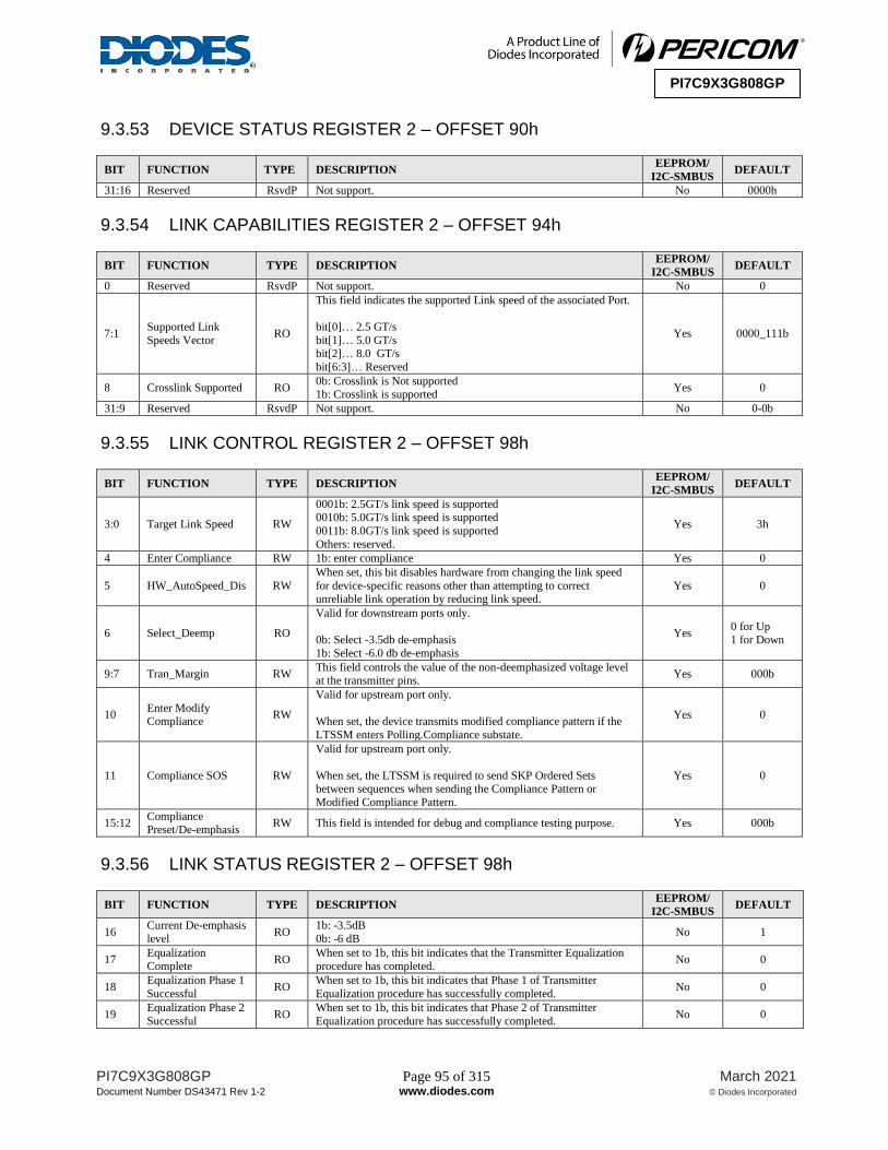
PI7C9X3G808GP Page 95 of 315 March 2021
Document Number DS43471 Rev 1-2 www.diodes.com © Diodes Incorporated
PI7C9X3G808GP
9.3.53 DEVICE STATUS REGISTER 2 – OFFSET 90h
BIT FUNCTION TYPE DESCRIPTION EEPROM/
I2C-SMBUS DEFAULT
31:16 Reserved RsvdP Not support. No 0000h
9.3.54 LINK CAPABILITIES REGISTER 2 – OFFSET 94h
BIT FUNCTION TYPE DESCRIPTION EEPROM/
I2C-SMBUS DEFAULT
0 Reserved RsvdP Not support. No 0
7:1 Supported Link
Speeds Vector RO
This field indicates the supported Link speed of the associated Port.
bit[0]… 2.5 GT/s
bit[1]… 5.0 GT/s bit[2]… 8.0 GT/s
bit[6:3]… Reserved
Yes 0000_111b
8 Crosslink Supported RO 0b: Crosslink is Not supported 1b: Crosslink is supported
Yes 0
31:9 Reserved RsvdP Not support. No 0-0b
9.3.55 LINK CONTROL REGISTER 2 – OFFSET 98h
BIT FUNCTION TYPE DESCRIPTION EEPROM/
I2C-SMBUS DEFAULT
3:0 Target Link Speed RW
0001b: 2.5GT/s link speed is supported 0010b: 5.0GT/s link speed is supported
0011b: 8.0GT/s link speed is supported
Others: reserved.
Yes 3h
4 Enter Compliance RW 1b: enter compliance Yes 0
5 HW_AutoSpeed_Dis RW
When set, this bit disables hardware from changing the link speed
for device-specific reasons other than attempting to correct unreliable link operation by reducing link speed.
Yes 0
6 Select_Deemp RO
Valid for downstream ports only.
0b: Select -3.5db de-emphasis
1b: Select -6.0 db de-emphasis
Yes 0 for Up 1 for Down
9:7 Tran_Margin RW This field controls the value of the non-deemphasized voltage level at the transmitter pins.
Yes 000b
10 Enter Modify Compliance
RW
Valid for upstream port only.
When set, the device transmits modified compliance pattern if the
LTSSM enters Polling.Compliance substate.
Yes 0
11 Compliance SOS RW
Valid for upstream port only.
When set, the LTSSM is required to send SKP Ordered Sets between sequences when sending the Compliance Pattern or
Modified Compliance Pattern.
Yes 0
15:12 Compliance Preset/De-emphasis
RW This field is intended for debug and compliance testing purpose. Yes 000b
9.3.56 LINK STATUS REGISTER 2 – OFFSET 98h
BIT FUNCTION TYPE DESCRIPTION EEPROM/
I2C-SMBUS DEFAULT
16 Current De-emphasis
level RO
1b: -3.5dB
0b: -6 dB No 1
17 Equalization
Complete RO
When set to 1b, this bit indicates that the Transmitter Equalization
procedure has completed. No 0
18 Equalization Phase 1
Successful RO
When set to 1b, this bit indicates that Phase 1 of Transmitter
Equalization procedure has successfully completed. No 0
19 Equalization Phase 2
Successful RO
When set to 1b, this bit indicates that Phase 2 of Transmitter
Equalization procedure has successfully completed. No 0

PI7C9X3G808GP Page 96 of 315 March 2021
Document Number DS43471 Rev 1-2 www.diodes.com © Diodes Incorporated
PI7C9X3G808GP
BIT FUNCTION TYPE DESCRIPTION EEPROM/
I2C-SMBUS DEFAULT
20 Equalization Phase 3 Successful
RO When set to 1b, this bit indicates that Phase 3 of Transmitter Equalization procedure has successfully completed.
No 0
21 Link Equalization
Request RW1C
This bit is set by hardware to request the Link equalization process
to be performed on the link. Yes 0
27:22 Reserved RsvdP Not support. No 0-0b
30:28 Downstream Component Presence
RO
This field indicates the presence and DRS status for the
Downstream Component.
000b: Link Down – Presence Not Determined 001b: Link Down – Component Not Present
010b: Link Down – Component Present
011b: Reserved
100b: Link Up – Component Present
101b: Link Up – Component Present and DRS Received 110b: Reserved
111b: Reserved
No 000b
31 DRS Message Received
RW1C This bit must be set whenever the Port receives a DRS message. Yes 0
9.3.57 SLOT CAPABILITIES REGISTER 2 – OFFSET 9Ch
BIT FUNCTION TYPE DESCRIPTION EEPROM/
I2C-SMBUS DEFAULT
31:0 Reserved RsvdP Not support. No 0000_0000h
9.3.58 SLOT CONTROL REGISTER 2 – OFFSET A0h
BIT FUNCTION TYPE DESCRIPTION EEPROM/
I2C-SMBUS DEFAULT
15:0 Reserved RsvdP Not support. No 0000_0000h
9.3.59 SLOT STATUS REGISTER 2 – OFFSET A0h
BIT FUNCTION TYPE DESCRIPTION EEPROM/
I2C-SMBUS DEFAULT
31:16 Reserved RsvdP Not support. No 0000_0000h
9.3.60 SSID/SSVID CAPATILITIES REGISTER – OFFSET A4h
BIT FUNCTION TYPE DESCRIPTION EEPROM/
I2C-SMBUS DEFAULT
7:0 SSID/SSVID Capabilities ID
RO Read as 0Dh to indicate that this is SSID/SSVID capability register. Yes 0Dh
15:8 Next Item Pointer RO Point to next PCI capability structure. Yes B0h for Up
00h for Down
31:16 Reserved RsvdP Not support. No 0000h
9.3.61 SUBSYSTEM VENDOR ID REGISTER – OFFSET A8h
BIT FUNCTION TYPE DESCRIPTION EEPROM/
I2C-SMBUS DEFAULT
15:0 SSVID RO It indicates the sub-system vendor id. Yes 12D8h
9.3.62 SUBSYSTEM ID REGISTER – OFFSET A8h
BIT FUNCTION TYPE DESCRIPTION EEPROM/
I2C-SMBUS DEFAULT
31:16 SSID RO It indicates the sub-system device id. Yes C008h

PI7C9X3G808GP Page 97 of 315 March 2021
Document Number DS43471 Rev 1-2 www.diodes.com © Diodes Incorporated
PI7C9X3G808GP
9.3.63 MSI-X CAPATILITIES REGISTER – OFFSET B0h (Upstream Port Only)
BIT FUNCTION TYPE DESCRIPTION EEPROM/
I2C-SMBUS DEFAULT
7:0 MSI-X Capabilities
ID RO Read as 11h to indicate that this is MSI-X capability register. No 11h
15:8 Next Item Pointer RO Read as 00h. No other ECP registers. Yes 00h
26:16 Table Size RO System software reads this field to determine the MSI-X Table Size
N, which is encoded as N-1. No 005h
29:27 Reserved RsvdP Not support, No 000b
30 Function Mask RW
If set, all of the vectors associated with the function are masked, regardless of their per-vector mask bit values.
If clear, each vector’s mask bit determines whether the vector is
masked or not.
Yes 0
31 MSI-X Enable RW
If set and the MSI Enable bit in the MSI Message Control register is
clear, the function is permitted to use MSI-X to request service and is prohibited from using INTx interrupts (if implemented).
If clear, the function is prohibited from using MSI-X to request
service.
Yes 0
9.3.64 MSI-X TABLE OFFSET/TABLE BIR REGISTER – OFFSET B4h (Upstream Port Only)
BIT FUNCTION TYPE DESCRIPTION EEPROM/
I2C-SMBUS DEFAULT
2:0 Table BIR RO
Read as 000b to indicate Base Address 0 register (offset 10h in
Configuration Space) is used to map the function MSI-X Table into
Memory space.
Yes 000b
31:3 Table Offset RO
Used as an offset from the address contained by one of the
function’s Base Address registers to point to the base of the MSI-X
Table.
Yes 0000_FE00h
9.3.65 MSI- X PBA OFFSET / PBA BIR REGISTER – OFFSET B8h (Upstream Port Only)
BIT FUNCTION TYPE DESCRIPTION EEPROM/
I2C-SMBUS DEFAULT
2:0 PBA BIR RO
Read as 000b to indicate Base Address 0 register (offset 10h in
Configuration Space) is used to map the function MSI-X PBA into
Memory space.
Yes 000b
31:3 PBA Offset RO
Used as an offset from the address contained by one of the
function’s Base Address registers to point to the base of the MSI-X
PBA.
Yes 0000_FE10h
9.3.66 BAR 0 CONFIGURATION REGISTER – OFFSET E0h (Upstream Port Only)
BIT FUNCTION TYPE DESCRIPTION EEPROM/
I2C-SMBUS DEFAULT
0 Type Selector RsvdP Not supported. No 0
2:1 BAR 0 Type RW 00b: BAR0 is implemented as a 32 bit Memory BAR
10b: BAR0/1 is implemented as a 64-bit Memory BAR Yes 00b
3 Prefetchable RW 0b: Non Prefetchable
1b: Prefetchable Yes 0
18:4 Reserved RsvdP Not supported. No 0-0b
30:19 BAR 0 Size RW
To specify BAR0 size.
0b: Corresponding BAR0 bits are RO bits that always return 0
1b: Corresponding BAR0 bits are RW bits
Yes FFFh
31
BAR 0 Enable RW bit[2:1]=00b 0b: Disable BAR0
1b: Enable BAR0 Yes 1
BAR 0 Size RW bit[2:1]=10b Includes with bit[30:19] when this BAR is used as a 64-bit BAR (bit[2:1]=10b).

PI7C9X3G808GP Page 98 of 315 March 2021
Document Number DS43471 Rev 1-2 www.diodes.com © Diodes Incorporated
PI7C9X3G808GP
9.3.67 BAR 0-1 CONFIGURATION REGISTER – OFFSET E4h (Upstream Port Only)
BIT FUNCTION TYPE DESCRIPTION EEPROM/
I2C-SMBUS DEFAULT
0 Type Selector
RsvdP E0h[2:1]=00b Not support. No 0
RW E0h[2:1]=10b BAR0/1 are used as a 64-bit BAR, bit[31:0] are used as the upper 32-bits.
Yes 0
2:1 BAR 1 Type
RO E0h[2:1]=00b 00b: BAR1 is implemented as 32 bit Memory
BAR. No 00b
RW E0h[2:1]=10b BAR0/1 are used as a 64-bit BAR, bit[31:0] are used as the upper 32-bits.
Yes 00b
3 Prefetchable
RW E0h[2:1]=00b 0b: Non Prefetchable
1b: Prefetchable Yes 0
RW E0h[2:1]=10b BAR0/1 are used as a 64-bit BAR, bit[31:0] are used as the upper 32-bits.
4 Reserved
RsvdP E0h[2:1]=00b Not support. No 0
RW E0h[2:1]=10b BAR0/1 are used as a 64-bit BAR, bit[31:0] are used as the upper 32-bits.
Yes 0
8:5 Domain ID
RW E0h[2:1]=00b The valid number is from 0 to 1.
Yes 0000b
RW E0h[2:1]=10b BAR0/1 are used as a 64-bit BAR, bit[31:0] are used as the upper 32-bits.
19:9 Reserved
RsvdP E0h[2:1]=00b Not support. No 0-0b
RW E0h[2:1]=10b BAR0/1 are used as a 64-bit BAR, bit[31:0] are used as the upper 32-bits.
Yes 0-0b
30:20 BAR 1 Size RW
To specify BAR1 size.
0b: Corresponding BAR1 bits are RO bits that always return 0
1b: Corresponding BAR1 bits are RW bits
Yes 000h
31
BAR 1 Enable RW E0h[2:1]=00b 0b: Disable BAR1 1b: Enable BAR1
Yes 0
64-Bit BAR RW E0h[2:1]=10b 0b: BAR0/1 is disabled, all BAR0/1 bits read 0.
1b: BAR0/1 is enabled as a 64-bit BAR.
9.3.68 PCI EXPRESS ADVANCED ERROR REPORTING ENHANCED CAPABILITY HEADER REGISTER – OFFSET 100h
BIT FUNCTION TYPE DESCRIPTION EEPROM/
I2C-SMBUS DEFAULT
15:0 Extended
Capabilities ID RO
Read as 0001h to indicate that this is PCI express extended
capability register for advance error reporting. No 0001h
19:16 Capability Version RO Read as 1h. No 1h
31:20 Next Capability
Offset RO Point to next PCI extended capability structure. Yes 130h
9.3.69 UNCORRECTABLE ERROR STATUS REGISTER – OFFSET 104h
BIT FUNCTION TYPE DESCRIPTION EEPROM/
I2C-SMBUS DEFAULT
0 Training Error Status RW1C When set, indicates that the Training Error event has occurred. Yes 0
3:1 Reserved RsvdP Not support. No 000
4 Data Link Protocol
Error Status RW1C
When set, indicates that the Data Link Protocol Error event has
occurred. Yes 0
5 Surprise Down Error
Status RW1C
When set, indicates that the Surprise Down Error event has occurred.
Valid for Downstream ports only.
Yes 0
11:6 Reserved RsvdP Not support. No 0-0b
12 Poisoned TLP Status RW1C When set, indicates that a Poisoned TLP has been received or
generated. Yes 0

PI7C9X3G808GP Page 99 of 315 March 2021
Document Number DS43471 Rev 1-2 www.diodes.com © Diodes Incorporated
PI7C9X3G808GP
BIT FUNCTION TYPE DESCRIPTION EEPROM/
I2C-SMBUS DEFAULT
13 Flow Control Protocol Error Status
RW1C When set, indicates that the Flow Control Protocol Error event has occurred.
Yes 0
14 Completion Timeout
Status RW1C
When set, indicates that the Completion Timeout event has
occurred. Yes 0
15 Completer
AbortStatus RW1C When set, indicates that the Completer Abort event has occurred. Yes 0
16 Unexpected Completion Status
RW1C When set, indicates that the Unexpected Completion event has occurred.
Yes 0
17 Receiver Overflow
Status RW1C When set, indicates that the Receiver Overflow event has occurred. Yes 0
18 Malformed TLP
Status RW1C
When set, indicates that a Malformed TLP has been received.
Yes 0
19 ECRC Error Status RW1C When set, indicates that an ECRC Error has been detected.
Yes 0
20 Unsupported Request
Error Status RW1C
When set, indicates that an Unsupported Request event has
occurred. Yes 0
21 ACS Violation Status RW1C
When set, indicates that an ACS Violation event has occurred.
Valid for Downstream ports only.
Yes 0
22 Internal Error Status RW1C When set, indicates that an internal error event has occurred. Yes 0
23 MC Blocked TLP
Status RW1C When set, indicates that an MC Blocked TLP event has occurred. Yes 0
24 AtomicOp Egress Blocked Status
RW1C When set, indicates that an AtomicOp Egress Blocked event has occurred.
Yes 0
31:25 Reserved RsvdP Not support. No 0000_000b
9.3.70 UNCORRECTABLE ERROR MASK REGISTER – OFFSET 108h
BIT FUNCTION TYPE DESCRIPTION EEPROM/
I2C-SMBUS DEFAULT
0 Training Error Mask RW When set, the Training Error event is not logged in the Header Log register and not issued as an Error Message to RC either.
Yes 0
3:1 Reserved RsvdP Not support. No 000b
4 Data Link Protocol
Error Mask RW
When set, the Data Link Protocol Error event is not logged in the
Header Log register and not issued as an Error Message to RC either.
Yes 0
5 Surprise Down Error
Mask RW
When set, Surprise Down Error event is not logged in the Header Log register and not issued as an Error Message to RC either.
Valid for Downstream ports only.
Yes 0
11:6 Reserved RsvdP Not support. No 0-0b
12 Poisoned TLP Mask RW
When set, an event of Poisoned TLP has been received or generated
is not logged in the Header Log register and not issued as an Error Message to RC either.
Yes 0
13 Flow Control
Protocol Error Mask RW
When set, the Flow Control Protocol Error event is not logged in the
Header Log register and not issued as an Error Message to RC either.
Yes 0
14 Completion Timeout
Mask RW
When set, the Completion Timeout event is not logged in the
Header Log register and not issued as an Error Message to RC either.
Yes 0
15 Completer
AbortMask RW
When set, the Completer Abort event is not logged in the Header
Log register and not issued as an Error Message to RC either.
Yes 0
16 Unexpected
Completion Mask RW
When set, the Unexpected Completion event is not logged in the
Header Log register and not issued as an Error Message to RC either.
Yes 0
17 Receiver Overflow
Mask RW
When set, the Receiver Overflow event is not logged in the Header
Log register and not issued as an Error Message to RC either. Yes 0
18 Malformed TLP Mask
RW
When set, an event of Malformed TLP has been received is not
logged in the Header Log register and not issued as an Error
Message to RC either.
Yes 0
19 ECRC Error Mask RW
When set, an event of ECRC Error has been detected is not logged
in the Header Log register and not issued as an Error Message to
RC either.
Yes 0

PI7C9X3G808GP Page 100 of 315 March 2021
Document Number DS43471 Rev 1-2 www.diodes.com © Diodes Incorporated
PI7C9X3G808GP
BIT FUNCTION TYPE DESCRIPTION EEPROM/
I2C-SMBUS DEFAULT
20 Unsupported Request Error Mask
RW When set, the Unsupported Request event is not logged in the Header Log register and not issued as an Error Message to RC
either.
Yes 0
21 ACS Violation Mask RW
When set, the ACS Violation event is not logged in the Header Log register and not issued as an Error Message to RC either.
Valid for Downstream ports only.
Yes 0
22 Internal Error Mask RW
When set, the Internal Error has been detected is not logged in the
Header Log register and not issued as an Error Message to RC either.
Yes 1
23 MC Blocked TLP
Mask RW
When set, the MC Blocked TLP event is not logged in the Header
Log register and not issued as an Error Message to RC either. Yes 0
24 AtomicOp Egress Blocked Mask
RW
When set, the AtomicOp Egress Blocked event is not logged in the
Header Log register and not issued as an Error Message to RC
either.
Yes 0
31:25 Reserved RsvdP Not support. No 0000_000b
9.3.71 UNCORRECTABLE ERROR SEVERITY REGISTER – OFFSET 10Ch
BIT FUNCTION TYPE DESCRIPTION EEPROM/
I2C-SMBUS DEFAULT
0 Training Error
Severity RW
0b: Non-Fatal
1b: Fatal Yes 1
3:1 Reserved RsvdP Not support. No 000b
4 Data Link Protocol
Error Severity RW
0b: Non-Fatal
1b: Fatal Yes 1
5 Surprise Down Error
Severity RW
0b: Non-Fatal
1b: Fatal
Valid for Downstream ports only.
Yes 0 for Up
1 for Down
11:6 Reserved RsvdP Not support. No 0-0b
12 Poisoned TLP
Severity RW
0b: Non-Fatal
1b: Fatal Yes 0
13
Flow Control
Protocol Error
Severity
RW 0b: Non-Fatal 1b: Fatal
Yes 1
14 Completion Timeout
Error Severity RW
0b: Non-Fatal
1b: Fatal Yes 0
15 Completer AbortSeverity
RW 0b: Non-Fatal 1b: Fatal
Yes 0
16 Unexpected
Completion Severity RW
0b: Non-Fatal
1b: Fatal Yes 0
17 Receiver Overflow
Severity RW
0b: Non-Fatal
1b: Fatal Yes 1
18 Malformed TLP Severity
RW 0b: Non-Fatal 1b: Fatal
Yes 1
19 ECRC Error Severity RW 0b: Non-Fatal
1b: Fatal Yes 0
20 Unsupported Request Error Severity
RW 0b: Non-Fatal 1b: Fatal
Yes 0
21 ACS Violation Severity
RW
0b: Non-Fatal
1b: Fatal
Valid for Downstream ports only.
Yes 0
22 Internal Error Severity
RW 0b: Non-Fatal 1b: Fatal
Yes 1
23 MC Blocked TLP Severity
RW 0b: Non-Fatal 1b: Fatal
Yes 0
24 AtomicOp Egress
Blocked Severity RW
0b: Non-Fatal
1b: Fatal Yes 0
31:25 Reserved RsvdP Not support. No 0000_000b
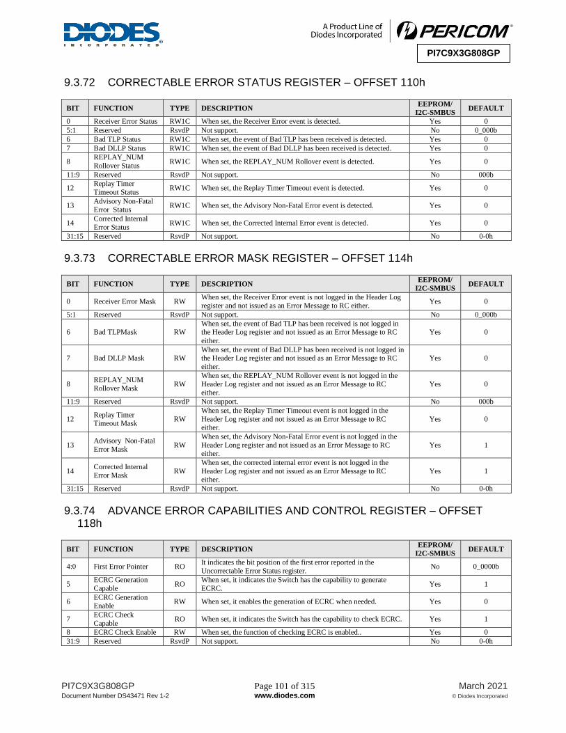
PI7C9X3G808GP Page 101 of 315 March 2021
Document Number DS43471 Rev 1-2 www.diodes.com © Diodes Incorporated
PI7C9X3G808GP
9.3.72 CORRECTABLE ERROR STATUS REGISTER – OFFSET 110h
BIT FUNCTION TYPE DESCRIPTION EEPROM/
I2C-SMBUS DEFAULT
0 Receiver Error Status RW1C When set, the Receiver Error event is detected. Yes 0
5:1 Reserved RsvdP Not support. No 0_000b
6 Bad TLP Status RW1C When set, the event of Bad TLP has been received is detected. Yes 0
7 Bad DLLP Status RW1C When set, the event of Bad DLLP has been received is detected. Yes 0
8 REPLAY_NUM
Rollover Status RW1C When set, the REPLAY_NUM Rollover event is detected. Yes 0
11:9 Reserved RsvdP Not support. No 000b
12 Replay Timer
Timeout Status RW1C When set, the Replay Timer Timeout event is detected. Yes 0
13 Advisory Non-Fatal Error Status
RW1C When set, the Advisory Non-Fatal Error event is detected. Yes 0
14 Corrected Internal
Error Status RW1C When set, the Corrected Internal Error event is detected. Yes 0
31:15 Reserved RsvdP Not support. No 0-0h
9.3.73 CORRECTABLE ERROR MASK REGISTER – OFFSET 114h
BIT FUNCTION TYPE DESCRIPTION EEPROM/
I2C-SMBUS DEFAULT
0 Receiver Error Mask RW When set, the Receiver Error event is not logged in the Header Log
register and not issued as an Error Message to RC either. Yes 0
5:1 Reserved RsvdP Not support. No 0_000b
6 Bad TLPMask RW When set, the event of Bad TLP has been received is not logged in the Header Log register and not issued as an Error Message to RC
either.
Yes 0
7 Bad DLLP Mask RW When set, the event of Bad DLLP has been received is not logged in the Header Log register and not issued as an Error Message to RC
either.
Yes 0
8 REPLAY_NUM Rollover Mask
RW
When set, the REPLAY_NUM Rollover event is not logged in the
Header Log register and not issued as an Error Message to RC
either.
Yes 0
11:9 Reserved RsvdP Not support. No 000b
12 Replay Timer Timeout Mask
RW
When set, the Replay Timer Timeout event is not logged in the
Header Log register and not issued as an Error Message to RC either.
Yes 0
13 Advisory Non-Fatal
Error Mask RW
When set, the Advisory Non-Fatal Error event is not logged in the
Header Long register and not issued as an Error Message to RC either.
Yes 1
14 Corrected Internal
Error Mask RW
When set, the corrected internal error event is not logged in the
Header Log register and not issued as an Error Message to RC
either.
Yes 1
31:15 Reserved RsvdP Not support. No 0-0h
9.3.74 ADVANCE ERROR CAPABILITIES AND CONTROL REGISTER – OFFSET 118h
BIT FUNCTION TYPE DESCRIPTION EEPROM/
I2C-SMBUS DEFAULT
4:0 First Error Pointer RO It indicates the bit position of the first error reported in the
Uncorrectable Error Status register. No 0_0000b
5 ECRC Generation
Capable RO
When set, it indicates the Switch has the capability to generate
ECRC. Yes 1
6 ECRC Generation Enable
RW When set, it enables the generation of ECRC when needed. Yes 0
7 ECRC Check
Capable RO When set, it indicates the Switch has the capability to check ECRC. Yes 1
8 ECRC Check Enable RW When set, the function of checking ECRC is enabled.. Yes 0
31:9 Reserved RsvdP Not support. No 0-0h

PI7C9X3G808GP Page 102 of 315 March 2021
Document Number DS43471 Rev 1-2 www.diodes.com © Diodes Incorporated
PI7C9X3G808GP
9.3.75 HEADER LOG REGISTER – OFFSET From 11Ch to 128h
BIT FUNCTION TYPE DESCRIPTION EEPROM/
I2C-SMBUS DEFAULT
31:0 1st DWORD RO Hold the 1st DWORD of TLP Header. The Head byte is in big
endian. No 0000_0000h
63:32 2nd DWORD RO Hold the 2nd DWORD of TLP Header. The Head byte is in big endian.
No 0000_0000h
95:64 3rd DWORD RO Hold the 3rd DWORD of TLP Header. The Head byte is in big
endian. No 0000_0000h
127:96 4th DWORD RO Hold the 4th DWORD of TLP Header. The Head byte is in big
endian. No 0000_0000h
9.3.76 PCI EXPRESS VIRTUAL CHANNEL ENHANCED CAPABILITYHEADER REGISTER – OFFSET 130h
BIT FUNCTION TYPE DESCRIPTION EEPROM/
I2C-SMBUS DEFAULT
15:0 Extended Capabilities ID
RO Read as 02h to indicate that this is PCI express extended capability register for virtual channel.
No 02h
19:16 Capability Version RO Read as 1h. No 01h
31:20 Next Capability
Offset RO Point to next PCI extended capability structure. Yes 1A0h
9.3.77 PORT VC CAPABILITY REGISTER 1 – OFFSET 134h
BIT FUNCTION TYPE DESCRIPTION EEPROM/
I2C-SMBUS DEFAULT
2:0 Extended VC Count RO It indicates the number of extended Virtual Channels in addition to
the default VC supported by the Switch. No 000b
3 Reserved RO Not support. No 0
6:4 Low Priority
Extended VC Count RO
It indicates the number of extended Virtual Channels in addition to
the default VC belonging to the low-priority VC (LPVC) group. No 000b
7 Reserved RO Not support. No 0
9:8 Reference Clock RO It indicates the reference clock for Virtual Channels that support time-based WRR Port Arbitration. Defined encoding is 00b for 100
ns reference clock.
No 00b
11:10 Port Arbitration Table Entry Size
RO Read as 10b to indicate the size of Port Arbitration table entry in the device is 4 bits.
No 10b
31:12 Reserved RsvdP Not support. No 0000_0h
9.3.78 PORT VC CAPABILITY REGISTER 2 – OFFSET 138h
BIT FUNCTION TYPE DESCRIPTION EEPROM/
I2C-SMBUS DEFAULT
7:0 VC Arbitration Capability
RO
It indicates the types of VC Arbitration supported by the device for the LPVC group. This field is valid when LPVC is greater
than 0. The Switch supports Hardware fixed arbitration scheme,
e.g., Round Robin and Weight Round Robin arbitration with 32 phases in LPVC.
No 00h
23:8 Reserved RsvdP Not support. No 0000h
31:24 VC Arbitration Table
Offset RO
It indicates the location of the VC Arbitration Table as an offset from the base address of the Virtual Channel Capability register
in the unit of DQWD (16 bytes).
No 00h
9.3.79 PORT VC CONTROL REGISTER – OFFSET 13Ch
BIT FUNCTION TYPE DESCRIPTION EEPROM/
I2C-SMBUS DEFAULT
0 Load VC Arbitration Table
WO When set, the programmed VC Arbitration Table is applied to the hardware. This bit always returns 0b when read.
Yes 0

PI7C9X3G808GP Page 103 of 315 March 2021
Document Number DS43471 Rev 1-2 www.diodes.com © Diodes Incorporated
PI7C9X3G808GP
BIT FUNCTION TYPE DESCRIPTION EEPROM/
I2C-SMBUS DEFAULT
3:1 VC Arbitration
Select RW
This field is used to configure the VC Arbitration by selecting one of the supported VC Arbitration schemes. The valid values for the
schemes supported by Switch are 0b and 1b. Other value than these written into this register will be treated as default.
Yes 000b
15:4 Reserved RsvdP Not support. No 000h
9.3.80 PORT VC STATUS REGISTER – OFFSET 13Ch
BIT FUNCTION TYPE DESCRIPTION EEPROM/
I2C-SMBUS DEFAULT
16 VC Arbitration Table Status
RO
When set, it indicates that any entry of the VC Arbitration Table is
written by software. This bit is cleared when hardware finishes loading values stored in the VC Arbitration Table after the bit of
“Load VC Arbitration Table” is set.
No 0
31:17 Reserved RsvdP Not support. No 0-0h
9.3.81 VC RESOURCE CAPABILITY REGISTER (0) – OFFSET 140h
BIT FUNCTION TYPE DESCRIPTION EEPROM/
I2C-SMBUS DEFAULT
7:0 Port Arbitration Capability
RO
It indicates the types of Port Arbitration supported by the VC
resource. The Switch supports Round Robin Hardware fixed arbitration scheme.
No 01h
13:8 Reserved RsvdP Not support. No 00_0000h
14 Advanced Packet
Switching RO
When set, it indicates the VC resource only supports transaction
optimized for Advanced Packet Switching (AS). No 0
15 Reject Snoop
Transactions RsvdP Not support. No 0
22:16 Maximum Time Slots
RO It indicates the maximum numbers of time slots (minus one) are allocated for Isochronous traffic.
No 3Fh
23 Reserved RsvdP Not support. No 0
31:24 Port Arbitration
Table Offset RO
It indicates the location of the Port Arbitration Table (n) as an offset from the base address of the Virtual Channel Capability register in
the unit of DQWD (16 bytes).
No 05h
9.3.82 VC RESOURCE CONTROL REGISTER (0) – OFFSET 144h
BIT FUNCTION TYPE DESCRIPTION EEPROM/
I2C-SMBUS DEFAULT
7:0 TC/VC Map RW
This field indicates the TCs that are mapped to the VC resource. Bit
locations within this field correspond to TC values. When the bits in
this field are set, it means that the corresponding TCs are mapped to
the VC resource. Bit 0 of this filed is read-only and must be set to “1” for the VC0.
Yes FFh
15:8 Reserved RsvdP Not support. No 00h
16 Load Port Arbitration
Table RW
When set, the programmed Port Arbitration Table is applied to the hardware.
This bit always returns 0b when read.
Yes 0
19:17 Port Arbitration Select
RW
This field is used to configure the Port Arbitration by selecting one of the supported Port Arbitration schemes. The permissible values
for the schemes supported by Switch are 000b and 011b at VC0,
other value than these written into this register will be treated as default.
Yes 000b
23:20 Reserved RsvdP Not support. No 0h
26:24 VC ID RO This field assigns a VC ID to the VC resource. No 000b
30:27 Reserved RsvdP Not support. No 0h
31 VC Enable RW 0b: it disables this Virtual Channel
1b: it enables this Virtual Channel Yes 1

PI7C9X3G808GP Page 104 of 315 March 2021
Document Number DS43471 Rev 1-2 www.diodes.com © Diodes Incorporated
PI7C9X3G808GP
9.3.83 VC RESOURCE STATUS REGISTER (0) – OFFSET 148h
BIT FUNCTION TYPE DESCRIPTION EEPROM/
I2C-SMBUS DEFAULT
15:0 Reserved RsvdP Not support. No 0000h
16 Port Arbitration Table Status
RO
When set, it indicates that any entry of the Port Arbitration Table is
written by software. This bit is cleared when hardware finishes loading values stored in the Port Arbitration Table after the bit of
“Load Port Arbitration Table” is set.
No 0
17 VC Negotiation Pending
RO When set, it indicates that the VC resource is still in the process of negotiation. This bit is cleared after the VC negotiation is complete.
No 1
31:18 Reserved RsvdP Not support. No 0-0h
9.3.84 DEVICE SERIAL NUMBER ENHANCED CAPABILITY HEADER REGISTER – OFFSET 1A0h
BIT FUNCTION TYPE DESCRIPTION EEPROM/
I2C-SMBUS DEFAULT
15:0 Extended
Capabilities ID RO
Read as 0003h to indicate that this is PCI express extended
capability register for device serial number. No 0003h
19:16 Capability Version RO Must be 1h for this version. No 1h
31:20 Next Capability
Offset RO Point to next PCI extended capability structure. Yes
1B0h for Up
1C0h for Down
9.3.85 DEVICE SERIAL NUMBER LOWER DW REGISTER – OFFSET 1A4h
BIT FUNCTION TYPE DESCRIPTION EEPROM/
I2C-SMBUS DEFAULT
31:0 Device serial number
1st DW RO First dword for device serial number. Yes 0000_12D8h
9.3.86 DEVICE SERIAL NUMBER HIGHER DW REGISTER – OFFSET 1A8h
BIT FUNCTION TYPE DESCRIPTION EEPROM/
I2C-SMBUS DEFAULT
31:0 Device serial number 2nd DW
RO 2nd dword for device serial number. Yes 0816_4896h
9.3.87 PCI EXPRESS POWER BUDGETING ENHANCED CAPABILITY HEADER REGISTER – OFFSET 1B0h (Upstream Port Only)
BIT FUNCTION TYPE DESCRIPTION EEPROM/
I2C-SMBUS DEFAULT
15:0 Extended
Capabilities ID RO
Read as 0004h to indicate that this is PCI express extended
capability register for power budgeting. No 0004h
19:16 Capability Version RO Must be 1h for this version. No 01h
31:20 Next Capability
Offset RO Point to next PCI extended capability structure. Yes 1D0h
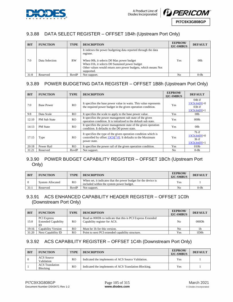
PI7C9X3G808GP Page 105 of 315 March 2021
Document Number DS43471 Rev 1-2 www.diodes.com © Diodes Incorporated
PI7C9X3G808GP
9.3.88 DATA SELECT REGISTER – OFFSET 1B4h (Upstream Port Only)
BIT FUNCTION TYPE DESCRIPTION EEPROM/
I2C-SMBUS DEFAULT
7:0 Data Selection RW
It indexes the power budgeting data reported through the data
register.
When 00h, it selects D0 Max power budget
When 01h, it selects D0 Sustained power budget Other values would return zero power budgets, which means Not
supported.
Yes 00h
31:8 Reserved RsvdP Not support. No 0-0h
9.3.89 POWER BUDGETING DATA REGISTER – OFFSET 1B8h (Upstream Port Only)
BIT FUNCTION TYPE DESCRIPTION EEPROM/
I2C-SMBUS DEFAULT
7:0 Base Power RO It specifies the base power value in watts. This value represents
the required power budget in the given operation condition. Yes
04h if
13Ch.bit[0]=0
03h if 13Ch.bit[0]=1
9:8 Data Scale RO It specifies the scale to apply to the base power value. Yes 00b
12:10 PM Sub State RO It specifies the power management sub state of the given operation condition. It is initialized to the default sub state.
Yes 000b
14:13 PM State RO It specifies the power management state of the given operation
condition. It defaults to the D0 power state. Yes 00b
17:15 Type RO It specifies the type of the given operation condition which is controlled by offset 13Ch[7:0]. It defaults to the Maximum
power state.
Yes
7h if 13Ch.bit[0]=0
3h if 13Ch.bit[0]=1
20:18 Power Rail RO It specifies the power rail of the given operation condition. Yes 010b
31:21 Reserved RsvdP Not support. No 0-0h
9.3.90 POWER BUDGET CAPABILITY REGISTER – OFFSET 1BCh (Upstream Port Only)
BIT FUNCTION TYPE DESCRIPTION EEPROM/
I2C-SMBUS DEFAULT
0 System Allocated RO When set, it indicates that the power budget for the device is included within the system power budget.
Yes 1
31:1 Reserved RsvdP Not support. No 0-0h
9.3.91 ACS ENHANCED CAPABILITY HEADER REGISTER – OFFSET 1C0h (Downstream Port Only)
BIT FUNCTION TYPE DESCRIPTION EEPROM/
I2C-SMBUS DEFAULT
15:0 PCI Express Extended Capability
ID
RO Read as 000Dh to indicate that this is PCI Express Extended Capability register for ACS. No 000Dh
19:16 Capability Version RO Must be 1h for this version. No 1h
31:20 Next Capability ID RO Point to next PCI extended capability structure. Yes 1D0h
9.3.92 ACS CAPABILITY REGISTER – OFFSET 1C4h (Downstream Port Only)
BIT FUNCTION TYPE DESCRIPTION EEPROM/
I2C-SMBUS DEFAULT
0 ACS Source
Validation RO Indicated the implements of ACS Source Validation. Yes 1
1 ACS Translation Blocking
RO Indicated the implements of ACS Translation Blocking. Yes 1
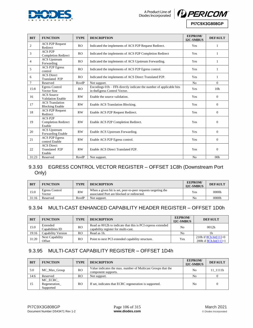
PI7C9X3G808GP Page 106 of 315 March 2021
Document Number DS43471 Rev 1-2 www.diodes.com © Diodes Incorporated
PI7C9X3G808GP
BIT FUNCTION TYPE DESCRIPTION EEPROM/
I2C-SMBUS DEFAULT
2 ACS P2P Request Redirect
RO Indicated the implements of ACS P2P Request Redirect. Yes 1
3 ACS P2P
Completion Redirect RO Indicated the implements of ACS P2P Completion Redirect Yes 1
4 ACS Upstream
Forwarding RO Indicated the implements of ACS Upstream Forwarding. Yes 1
5 ACS P2P Egress control
RO Indicated the implements of ACS P2P Egress control. Yes 1
6 ACS Direct
Translated P2P RO Indicated the implements of ACS Direct Translated P2P. Yes 1
7 Reserved RsvdP Not support. No 0
15:8 Egress Control
Vector Size RO
Encodings 01h – FFh directly indicate the number of applicable bits
in theEgress Control Vector. Yes 10h
16 ACS Source Validation Enable
RW Enable the source validation. Yes 0
17 ACS Translation Blocking Enable
RW Enable ACS Translation Blocking. Yes 0
18 ACS P2P Request
Redirect RW Enable ACS P2P Request Redirect. Yes 0
19 ACS P2P Completion Redirect
Enable
RW Enable ACS P2P Completion Redirect. Yes 0
20 ACS Upstream Forwarding Enable
RW Enable ACS Upstream Forwarding. Yes 0
21 ACS P2P Egress
control Enable RW Enable ACS P2P Egress control. Yes 0
22
ACS Direct
Translated P2P
Enable
RW Enable ACS Direct Translated P2P. Yes 0
31:23 Reserved RsvdP Not support. No 00h
9.3.93 EGRESS CONTROL VECTOR REGISTER – OFFSET 1C8h (Downstream Port Only)
BIT FUNCTION TYPE DESCRIPTION EEPROM/
I2C-SMBUS DEFAULT
15:0 Egress Control
Vector RW
When a given bit is set, peer-to-peer requests targeting the
associated Port are blocked or redirected. Yes 0000h
31:16 Reserved RsvdP Not support. No 0000h
9.3.94 MULTI-CAST ENHANCED CAPABILITY HEADER REGISTER – OFFSET 1D0h
BIT FUNCTION TYPE DESCRIPTION EEPROM/
I2C-SMBUS DEFAULT
15:0 Extended
Capabilities ID RO
Read as 0012h to indicate that this is PCI express extended
capability register for multi-cast. No 0012h
19:16 Capability Version RO Read as 1h. No 1h
31:20 Next Capability
Offset RO Point to next PCI extended capability structure. Yes
210h if 8Ch.bit[11]=0
200h if 8Ch.bit[11]=1
9.3.95 MULTI-CAST CAPABILITY REGISTER – OFFSET 1D4h
BIT FUNCTION TYPE DESCRIPTION EEPROM/
I2C-SMBUS DEFAULT
5:0 MC_Max_Group RO Value indicates the max. number of Multicast Groups that the component supports.
No 11_1111b
14:6 Reserved RO Not support. No 0
15
MC_ECRC_
Regeneration_ Supported
RO If set, indicates that ECRC regeneration is supported. No 0
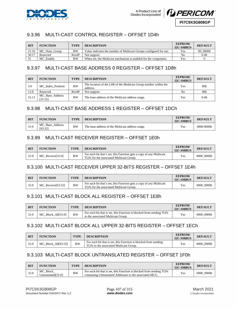
PI7C9X3G808GP Page 107 of 315 March 2021
Document Number DS43471 Rev 1-2 www.diodes.com © Diodes Incorporated
PI7C9X3G808GP
9.3.96 MULTI-CAST CONTROL REGISTER – OFFSET 1D4h
BIT FUNCTION TYPE DESCRIPTION EEPROM/
I2C-SMBUS DEFAULT
21:16 MC_Num_Group RW Value indicates the number of Multicast Groups configured for use. Yes 00_0000b
30:17 Reserved RsvdP Not support. No 0-0h
31 MC_Enable RW When set, the Multicast mechanism is enabled for the component. Yes 0
9.3.97 MULTI-CAST BASE ADDRESS 0 REGISTER – OFFSET 1D8h
BIT FUNCTION TYPE DESCRIPTION EEPROM/
I2C-SMBUS DEFAULT
5:0 MC_Index_Position RW The location of the LSB of the Multicast Group number within the address.
Yes 00h
11:6 Reserved RsvdP Not support. No 00h
31:12 MC_Base_Address [31:12]
RW The base address of the Multicast address range. Yes 0-0h
9.3.98 MULTI-CAST BASE ADDRESS 1 REGISTER – OFFSET 1DCh
BIT FUNCTION TYPE DESCRIPTION EEPROM/
I2C-SMBUS DEFAULT
31:0 MC_Base_Address
[63:32] RW The base address of the Multicast address range. Yes 0000-0000h
9.3.99 MULTI-CAST RECEIVER REGISTER – OFFSET 1E0h
BIT FUNCTION TYPE DESCRIPTION EEPROM/
I2C-SMBUS DEFAULT
31:0 MC_Receive[31:0] RW For each bit that’s set, this Function gets a copy of any Multicast TLPs for the associated Multicast Group.
Yes 0000_0000h
9.3.100 MULTI-CAST RECEIVER UPPER 32-BITS REGISTER – OFFSET 1E4h
BIT FUNCTION TYPE DESCRIPTION EEPROM/
I2C-SMBUS DEFAULT
31:0 MC_Receive[63:32] RW For each bit that’s set, this Function gets a copy of any Multicast
TLPs for the associated Multicast Group. Yes 0000_0000h
9.3.101 MULTI-CAST BLOCK ALL REGISTER – OFFSET 1E8h
BIT FUNCTION TYPE DESCRIPTION EEPROM/
I2C-SMBUS DEFAULT
31:0 MC_Block_All[31:0] RW For each bit that is set, this Function is blocked from sending TLPs
to the associated Multicast Group. Yes 0000_0000h
9.3.102 MULTI-CAST BLOCK ALL UPPER 32-BITS REGISTER – OFFSET 1ECh
BIT FUNCTION TYPE DESCRIPTION EEPROM/
I2C-SMBUS DEFAULT
31:0 MC_Block_All[63:32] RW For each bit that is set, this Function is blocked from sending TLPs to the associated Multicast Group.
Yes 0000_0000h
9.3.103 MULTI-CAST BLOCK UNTRANSLATED REGISTER – OFFSET 1F0h
BIT FUNCTION TYPE DESCRIPTION EEPROM/
I2C-SMBUS DEFAULT
31:0 MC_Block_
Untranslated[31:0] RW
For each bit that is set, this Function is blocked from sending TLPs
containing Untranslated Addresses to the associated MCG. Yes 0000_0000h

PI7C9X3G808GP Page 108 of 315 March 2021
Document Number DS43471 Rev 1-2 www.diodes.com © Diodes Incorporated
PI7C9X3G808GP
9.3.104 MULTI-CAST BLOCK UNTRANSLATED UPPER 32-BITS REGISTER – OFFSET 1F4h
BIT FUNCTION TYPE DESCRIPTION EEPROM/
I2C-SMBUS DEFAULT
31:0 MC_Block_
Untranslated[63:32] RW
For each bit that is set, this Function is blocked from sending TLPs
containing Untranslated Addresses to the associated MCG. Yes 0000_0000h
9.3.105 LTR EXTENDED CAPABILITY HEADER – OFFSET 200h (Upstream Port Only)
BIT FUNCTION TYPE DESCRIPTION EEPROM/
I2C-SMBUS DEFAULT
15:0
PCI Express
Extended Capability
ID
RO Read as 0018h to indicate that this is PCI Express Extended Capability register for LTR.
No 0018h if 8Ch.bit[11]=1 0000h if 8Ch.bit[11]=0
19:16 Capability Version RO Must be 1h for this version. No 1h if 8Ch.bit[11]=1
0h if 8Ch.bit[11]=0
31:20 Next Capability ID RO Point to next PCI extended capability structure. Yes 210h if 8Ch.bit[11]=1 000h if 8Ch.bit[11]=0
9.3.106 MAX SNOOP LATENCY REGISTER – OFFSET 204h (Upstream Port Only)
BIT FUNCTION TYPE DESCRIPTION EEPROM/
I2C-SMBUS DEFAULT
9:0 Max Snoop Latency
Value RW
Specifies the maximumsnoop latency that a device is
permitted to request Yes
0D0h if 8Ch.bit[11]=1
000h if 8Ch.bit[11]=0
12:10 Max Snoop Latency Scale
RW This register provides a scalefor the value contained within the Maximum SnoopLatencyValue field
Yes 000b
15:13 Reserved RsvdP Not support. No 000b
9.3.107 MAX NO-SNOOP LATENCY REGISTER – OFFSET 204h (Upstream Port Only)
BIT FUNCTION TYPE DESCRIPTION EEPROM/
I2C-SMBUS DEFAULT
25:16 Max No-Snoop Latency Value
RW Specifies the maximum no-snoop latency that a device is permitted to request
Yes 0D0h if 8Ch.bit[11]=1 000h if 8Ch.bit[11]=0
28:26 Max No-Snoop
Latency Scale RW
This register provides a scalefor the value contained
within the Maximum No-SnoopLatencyValue field Yes 000b
31:29 Reserved RsvdP Not support. No 000b
9.3.108 SECONDARY PCI EXPRESS EXTENDED CAPABILITY HEADER – OFFSET 210h
BIT FUNCTION TYPE DESCRIPTION EEPROM/
I2C-SMBUS DEFAULT
15:0
PCI Express
Extended Capability ID
RO Read as 0019h to indicate that this is PCI Express Extended Capability register for Secondary PCI Express.
No 0019h
19:16 Capability Version RO Must be 1h for this version. No 1h
31:20 Next Capability ID RO Point to next PCI extended capability structure. Yes
2B0h for Up
2A0h for Down

PI7C9X3G808GP Page 109 of 315 March 2021
Document Number DS43471 Rev 1-2 www.diodes.com © Diodes Incorporated
PI7C9X3G808GP
9.3.109 LINK CONTROL 3 REGISTER – OFFSET 214h
BIT FUNCTION TYPE DESCRIPTION EEPROM/
I2C-SMBUS DEFAULT
0 Perform Equalization RW
When this bit is 1b and a 1b is written to the Retrain Link bit with
the Target Link Speed field set to 8.0 GT/s, the downstream port must perform Link Equalization.
Yes 0
1
Link Equalization
Request Interrupt Enable
RW When set, this bit enables the generation of an interrupt to indicate that the Link Equalization bit has been set.
Yes 0
31:2 Reserved RsvdP Not support. No 0000h
9.3.110 LANE ERROR STATUS REGISTER – OFFSET 218h
BIT FUNCTION TYPE DESCRIPTION EEPROM/
I2C-SMBUS DEFAULT
31:0 Lane Error Status RW1C Each bit indicates if the corresponding Lane detected a Lane-base
error. Yes 0000_0000h
9.3.111 LANE EQUALIZATION CONTROL REGISTER – OFFSET 21Ch – 230h
Table 9-2 Lane Equalization Control Register Locations CFG_OFFSET Lane Number CFG_OFFSET Lane Number
21Ch 0 22Ch 4
21Eh 1 22Eh 5
220h 2 230h 6
222h 3 232h 7
Table 9-3 Lane Equalization Control Register Definitions
BIT FUNCTION TYPE DESCRIPTION EEPROM/
I2C-SMBUS DEFAULT
3:0 Downstream Port
Transmitter Preset RW
Transmitter Preset used for equalization by this Port when the Port is operating as a Downstream Port. This field is ignored when the
Port is operating as an Upstream Port.
Yes 0h for Up
8h for Down
7:4 Downstream Port
Receiver Preset Hint RW
Receiver Preset Hint may be used as a hint for receiver equalization by this Port when the Port is operating as a Downstream Port. This
field is ignored when the Port is operating as an Upstream Port.
Yes 0h for Up
2h for Down
11:8 Upstream Port
Transmitter Preset RO
For downstream ports, Field contains the Transmit Preset value sent or received during Link Equalization.
For upstream port, it is debugged used only.
Yes 8h
14:12 Upstream Port Receiver Preset Hint
RO
For downstream ports, Field contains the Receiver Preset Hint value
sent or received during Link Equalization.
For upstream port, it is debugged used only.
Yes 2h
15 Reserved RsvdP Not support. No 0
31:16 Reserved RW Internal used only. No 0000h
9.3.112 DPC EXTENDED CAPABILITY HEADER – OFFSET 2A0h (Downstream Port Only)
BIT FUNCTION TYPE DESCRIPTION EEPROM/
I2C-SMBUS DEFAULT
15:0
PCI Express
Extended Capability
ID
RO
Read as 001Dh to indicate that this is PCI Express Extended
Capability register for DPC. No 001Dh
19:16 Capability Version RO Must be 1h for this version. No 1h
31:20 Next Capability ID RO Point to next PCI extended capability structure. Yes 2B0h
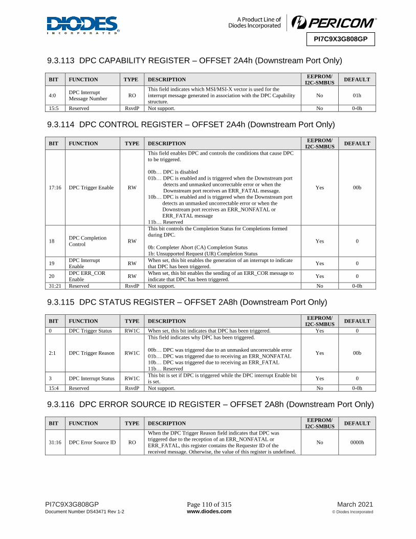
PI7C9X3G808GP Page 110 of 315 March 2021
Document Number DS43471 Rev 1-2 www.diodes.com © Diodes Incorporated
PI7C9X3G808GP
9.3.113 DPC CAPABILITY REGISTER – OFFSET 2A4h (Downstream Port Only)
BIT FUNCTION TYPE DESCRIPTION EEPROM/
I2C-SMBUS DEFAULT
4:0 DPC Interrupt Message Number
RO
This field indicates which MSI/MSI-X vector is used for the
interrupt message generated in association with the DPC Capability structure.
No 01h
15:5 Reserved RsvdP Not support. No 0-0h
9.3.114 DPC CONTROL REGISTER – OFFSET 2A4h (Downstream Port Only)
BIT FUNCTION TYPE DESCRIPTION EEPROM/
I2C-SMBUS DEFAULT
17:16 DPC Trigger Enable RW
This field enables DPC and controls the conditions that cause DPC
to be triggered.
00b… DPC is disabled 01b… DPC is enabled and is triggered when the Downstream port
detects and unmasked uncorrectable error or when the
Downstream port receives an ERR_FATAL message. 10b… DPC is enabled and is triggered when the Downstream port
detects an unmasked uncorrectable error or when the Downstream port receives an ERR_NONFATAL or
ERR_FATAL message
11b… Reserved
Yes 00b
18 DPC Completion
Control RW
This bit controls the Completion Status for Completions formed
during DPC.
0b: Completer Abort (CA) Completion Status
1b: Unsupported Request (UR) Completion Status
Yes 0
19 DPC Interrupt Enable
RW When set, this bit enables the generation of an interrupt to indicate that DPC has been triggered.
Yes 0
20 DPC ERR_COR
Enable RW
When set, this bit enables the sending of an ERR_COR message to
indicate that DPC has been triggered. Yes 0
31:21 Reserved RsvdP Not support. No 0-0h
9.3.115 DPC STATUS REGISTER – OFFSET 2A8h (Downstream Port Only)
BIT FUNCTION TYPE DESCRIPTION EEPROM/
I2C-SMBUS DEFAULT
0 DPC Trigger Status RW1C When set, this bit indicates that DPC has been triggered. Yes 0
2:1 DPC Trigger Reason RW1C
This field indicates why DPC has been triggered.
00b… DPC was triggered due to an unmasked uncorrectable error
01b… DPC was triggered due to receiving an ERR_NONFATAL 10b… DPC was triggered due to receiving an ERR_FATAL
11b… Reserved
Yes 00b
3 DPC Interrupt Status RW1C This bit is set if DPC is triggered while the DPC interrupt Enable bit is set.
Yes 0
15:4 Reserved RsvdP Not support. No 0-0h
9.3.116 DPC ERROR SOURCE ID REGISTER – OFFSET 2A8h (Downstream Port Only)
BIT FUNCTION TYPE DESCRIPTION EEPROM/
I2C-SMBUS DEFAULT
31:16 DPC Error Source ID RO
When the DPC Trigger Reason field indicates that DPC was triggered due to the reception of an ERR_NONFATAL or
ERR_FATAL, this register contains the Requester ID of the
received message. Otherwise, the value of this register is undefined.
No 0000h

PI7C9X3G808GP Page 111 of 315 March 2021
Document Number DS43471 Rev 1-2 www.diodes.com © Diodes Incorporated
PI7C9X3G808GP
9.3.117 LI PM SUBSTATES ENHANCED CAPABILITY HEADER – OFFSET 2B0h
BIT FUNCTION TYPE DESCRIPTION EEPROM/
I2C-SMBUS DEFAULT
15:0
PCI Express
Extended Capability ID
RO Read as 001Eh to indicate that this is PCI Express Extended Capability register for L1 PM Substates.
No 001Eh
19:16 Capability Version RO Must be 1h for this version. No 1h
31:20 Next Capability ID RO Point to next PCI extended capability structure. Yes 300h
9.3.118 L1 PM SUBSTATES CAPABILITY REGISTER – OFFSET 2B4h
BIT FUNCTION TYPE DESCRIPTION EEPROM/
I2C-SMBUS DEFAULT
0 PCI-PM L1.2 Supported
RO When set this bit indicates that PCI-PM L1.2 is supported. Yes 0
1 PCI-PM L1.1
Supported RO
When set this bit indicates that PCI-PM L1.1 is supported and must
be set by all ports implementing L1 PM Substates. Yes 0
2 ASPM L1.2 Supported
RO When set this bit indicates that ASPM L1.2 is supported. Yes 0
3 ASPM L1.1
Supported RO When set this bit indicates that ASPM L1.1 is supported. Yes 0
4 L1 PM Substates
Supported RO When set this bit indicates that this port supports L1 PM Substates. Yes 1
31:5 Reserved RsvdP Not support. No 0-0h
9.3.119 L1 PM SUBSTATES CONTROL 1 REGISTER – OFFSET 2B8h
BIT FUNCTION TYPE DESCRIPTION EEPROM/
I2C-SMBUS DEFAULT
0 PCI-PM L1.2 Enable RW When set this bit enables PCI-PM L1.2. Required for both upstream
and downstream ports. Yes 0
1 PCI-PM L1.1 Enable RW When set this bit enables PCI-PM L1.1. Required for both upstream and downstream ports.
Yes 0
2 ASPM L1.2 Enable RW When set this bit enables ASPM L1.2. Required for both upstream
and downstream ports. Yes 0
3 ASPM L1.1 Enable RW When set this bit enables ASPM L1.1. Required for both upstream and downstream ports.
Yes 0
31:4 Reserved RsvdP Not support. No 0-0h
9.3.120 L1 PM SUBSTATES CONTROL 2 REGISTER – OFFSET 2BCh
BIT FUNCTION TYPE DESCRIPTION EEPROM/
I2C-SMBUS DEFAULT
31:0 Reserved RsvdP Not support. No 0000_0000h
9.3.121 VENDOR-SPECIFIC ENHANCED CAPABILITY HEADER – OFFSET 300h
BIT FUNCTION TYPE DESCRIPTION EEPROM/
I2C-SMBUS DEFAULT
15:0 PCI Express Extended Capability
ID
RO Read as 000Bh to indicate that this is PCI Express Extended Capability register for Vendor-Specific.
No 000Bh
19:16 Capability Version RO Must be 1h for this version. No 1h
31:20 Next Capability ID RO Points to 000h. No 000h

PI7C9X3G808GP Page 112 of 315 March 2021
Document Number DS43471 Rev 1-2 www.diodes.com © Diodes Incorporated
PI7C9X3G808GP
9.3.122 VENDOR-SPECIFIC HEADER – OFFSET 304h
BIT FUNCTION TYPE DESCRIPTION EEPROM/
I2C-SMBUS DEFAULT
15:0 VSEC ID RO This field is a vendor-defined ID number that indicates the nature
and format of the VSEC structure. Yes 0000h
19:16 VSEC Rev RO This field is a vendor-defined version number that indicates the version of the VSEC structure.
No 0h
31:20 VSEC Length RO This field indicates the number of bytes in the entire VSEC
structure. Yes 560h
9.3.123 EEPROM CONTROL REGISTER – OFFSET 308h (Upstream Port Only)
BIT FUNCTION TYPE DESCRIPTION EEPROM/
I2C-SMBUS DEFAULT
0 EEPROM Start RW
Starts the EEPROM read or write cycle. This bit will auto clear to 0
when access is completed.
1b: start read or write cycle
Yes 0
3:1 Reserved RsvdP Not support. No 000b
4 EEPROM Autoload Status
RO 0b: EEPROM autoload is unsuccessful or is disabled 1b: EEPROM autoload is successful after PERST_L.
No 0
5 EEPROM is in
programming mode RO
0b: EEPROM is in auto-load mode
1b: EEPROM is in programming mode Yes 1
7:6 EEPROM Clock
Rate RW
Determines the frequency of the EEPROM clock which is derived from the primary clock.
00b: 500MHz/128
01b: 500MHz/(128*2)
10b: 500MHz/(128*4) 11b: 500MHz/(128*8)
Yes 00b
15:8 EEPROM Status RO Indicates the EEPROM status reflected by EEPROM read command.
No 00h
23:16 EEPROM Command RW
01h: write STATUS register
02h: EEPROM write 03h: EEPROM read
04h: disable write operation
05h: read STATUS register 06h: enable write operation
C7h: erase entire EEPROM
Yes 00h
30:24 Reserved RsvdP Not support. No 00h
31 Size 64K Mode RW 0b: EEPROM size is less or equal to 64K
1b: EEPROM size is larger 64K Yes 0
9.3.124 EEPROM ADDRESS AND DATA REGISTER – OFFSET 30Ch (Upstream Port Only)
BIT FUNCTION TYPE DESCRIPTION EEPROM/
I2C-SMBUS DEFAULT
15:0 EEPROM Address RW Contains the EEPROM address. Yes 0000h
31:16 EEPROM Data RW Contains the EEPROM data. Yes 0000h
9.3.125 DEBUGOUT CONTROL REGISTER – OFFSET 310h (Port 0 Only)
BIT FUNCTION TYPE DESCRIPTION EEPROM/
I2C-SMBUS DEFAULT
4:0 Debug Mode Select RW
Debug mode select. Selects a signal group for probing the current
internal status. For example, “0” represents LTSSM signal group.
As to other values, please inquire internal team for further information,
Yes 0_0000b
7:5 Debug
Port_Select_S1 RW
Debug port select s1. Selects a port number for monitoring at a
given signal group. Yes 000b

PI7C9X3G808GP Page 113 of 315 March 2021
Document Number DS43471 Rev 1-2 www.diodes.com © Diodes Incorporated
PI7C9X3G808GP
BIT FUNCTION TYPE DESCRIPTION EEPROM/
I2C-SMBUS DEFAULT
8 DebugPort_ Select_S2
RW Debugport select s2. Yes 0
9 Debug Output Start RW Start to capture debug output data. Yes 0
31:10 Reserved RsvdP Not support. No 0-0h
9.3.126 DEBUGOUT DATA REGISTER – OFFSET 314h (Port 0 Only)
BIT FUNCTION TYPE DESCRIPTION EEPROM/
I2C-SMBUS DEFAULT
9:0 Debug Output Data RO
Content of the debug output data.
For example, if LTSSM signal group is selected, the meaning of debug output data is as follows.
001h: detect
002h: polling
004h: configuration 008h: L0
010h: L1 020h: L2
040h: disable
080h: hot-reset 100h: loopback
200h: recovery Others: Reserved
No 000h
31:10 Reserved RsvdP Not support No 0000_0h
9.3.127 SMBUS CONTROL AND STATUS REGISTER – OFFSET 318h (Port 0 Only)
BIT FUNCTION TYPE DESCRIPTION EEPROM/
I2C-SMBUS DEFAULT
0 SMBus Enabled RW
Used to set SMBUS_EN_L strap pin.
0b: SMBus is disabled while I2C is enabled
1b: SMBus is enabled while I2C is disabled
Yes 1
3:1 I2C/SMBUS Address
[2:0] RW Used to set I2C/SMBUS Address[2:0]. Yes
Set by I2C_ADDRESS
[2:0]
7:4 I2C/SMBUS Address [6:3]
RW Used to set I2C/SMBUS Address[6:3]. Yes 1101b
8 ARP_Disable RW Test used only. Yes 1
9 PEC Check Disable RW 0b: enable PEC check
1b: disable PEC check Yes 1
10 AV Flag RW Test used only. Yes 0
11 AR Flag RW Test used only. Yes 0
13:12 UDID Addr Type RW Test used only. Yes 00b
14 UDID PEC Support RW Test used only. Yes 1
15 Cross Strapping
Done RO Test used only. No 0
23:16 UDID Vendor ID RW Test used only. Yes B0h
26:24 UDID Revision ID RW Test used only. Yes 001b
27 Fty Test 0 RW Test used only. Yes 0
28 SMBUS In Progress RO 0b: SMBUS interface is idle 1b: SMBUS interface is busy
No 0
29 PEC Check Fail RO 0b: PEC check successfully
1b: PEC check failed No 0
30 Unsupported
SMBUS Command RO
0b: supported command
1b: unsupported command No 0
31 Reserved RO Not support. No 1

PI7C9X3G808GP Page 114 of 315 March 2021
Document Number DS43471 Rev 1-2 www.diodes.com © Diodes Incorporated
PI7C9X3G808GP
9.3.128 GPIO 0-15 DIRECTION CONTROL REGISTER – OFFSET 31Ch (Port 0 Only)
BIT FUNCTION TYPE DESCRIPTION EEPROM/
I2C-SMBUS DEFAULT
0 GPIO[0]
Source/Destination RW
As Input:
0b: Input Data Register (offset 328h[0]) 1b: General Interrupt (INTx, or MSI)
As Output:
0b: From GPIO[0] Output Data register (offset 330h[0]) 1b: Reserved
Yes 0
1 GPIO[0] Direction
Control RW
0: Input
1: Output Yes 0
2 GPIO[1] Source/Destination
RW
As Input:
0b: Input Data Register (offset 328h[1])
1b: General Interrupt (INTx, or MSI) As Output:
0b: From GPIO[1] Output Data register (offset 330h[1]) 1b: Reserved
Yes 0
3 GPIO[1] Direction
Control RW
0: Input
1: Output Yes 0
4 GPIO[2] Source/Destination
RW
As Input: 0b: Input Data Register (offset 328h[2])
1b: General Interrupt (INTx, or MSI) As Output:
0b: From GPIO[2] Output Data register (offset 330h[2])
1b: Reserved
Yes 0
5 GPIO[2] Direction
Control RW
0: Input
1: Output Yes 0
6 GPIO[3]
Source/Destination RW
As Input:
0b: Input Data Register (offset 328h[3])
1b: General Interrupt (INTx, or MSI)
As Output: 0b: From GPIO[3] Output Data register (offset 330h[3])
1b: Reserved
Yes 0
7 GPIO[3] Direction
Control RW
0: Input
1: Output Yes 0
8 GPIO[4]
Source/Destination RW
As Input: 0b: Input Data Register (offset 328h[4])
1b: General Interrupt (INTx, or MSI)
As Output: 0b: From GPIO[4] Output Data register (offset 330h[4])
1b: Reserved
Yes 0
9 GPIO[4] Direction Control
RW 0: Input 1: Output
Yes 0
10 GPIO[5]
Source/Destination RW
As Input:
0b: Input Data Register (offset 328h[5]) 1b: General Interrupt (INTx, or MSI)
As Output: 0b: From GPIO[5] Output Data register (offset 330h[5])
1b: Reserved
Yes 0
11 GPIO[5] Direction Control
RW 0: Input 1: Output
Yes 0
12 GPIO[6]
Source/Destination RW
As Input:
0b: Input Data Register (offset 328h[6]) 1b: General Interrupt (INTx, or MSI)
As Output:
0b: From GPIO[6] Output Data register (offset 330h[6]) 1b: Reserved
Yes 0
13 GPIO[6] Direction
Control RW
0: Input
1: Output Yes 0
14 GPIO[7]
Source/Destination RW
As Input:
0b: Input Data Register (offset 328h[7]) 1b: General Interrupt (INTx, or MSI)
As Output:
0b: From GPIO[7] Output Data register (offset 330h[7]) 1b: Reserved
Yes 0

PI7C9X3G808GP Page 115 of 315 March 2021
Document Number DS43471 Rev 1-2 www.diodes.com © Diodes Incorporated
PI7C9X3G808GP
BIT FUNCTION TYPE DESCRIPTION EEPROM/
I2C-SMBUS DEFAULT
15 GPIO[7] Direction Control
RW 0: Input 1: Output
Yes 0
16 GPIO[8]
Source/Destination RW
As Input:
0b: Input Data Register (offset 328h[8]) 1b: General Interrupt (INTx, or MSI)
As Output: 0b: From GPIO[8] Output Data register (offset 330h[8])
1b: Reserved
Yes 0
17 GPIO[8] Direction Control
RW 0: Input 1: Output
Yes 0
18 GPIO[9]
Source/Destination RW
As Input:
0b: Input Data Register (offset 328h[9])
1b: General Interrupt (INTx, or MSI)
As Output: 0b: From GPIO[9] Output Data register (offset 330h[9])
1b: Resrved
Yes 0
19 GPIO[9] Direction Control
RW 0: Input 1: Output
Yes 0
20 GPIO[10]
Source/Destination RW
As Input:
0b: Input Data Register (offset 328h[10]) 1b: General Interrupt (INTx, or MSI)
As Output:
0b: From GPIO[10] Output Data register (offset 330h[10]) 1b: Reserved
Yes 0
21 GPIO[10] Direction
Control RW
0: Input
1: Output Yes 0
22 GPIO[11] Source/Destination
RW
As Input:
0b: Input Data Register (offset 328h[11])
1b: General Interrupt (INTx, or MSI) As Output:
0b: From GPIO[11] Output Data register (offset 330h[11]) 1b: Reserved
Yes 0
23 GPIO[11] Direction
Control RW
0: Input
1: Output Yes 0
24 GPIO[12] Source/Destination
RW
As Input:
0b: Input Data Register (offset 328h[12]))
1b: General Interrupt (INTx, or MSI) As Output:
0b: From GPIO[12] Output Data register (offset 330h[12]) 1b: Reserved
Yes 0
25 GPIO[12] Direction
Control RW
0: Input
1: Output Yes 0
26 GPIO[13] Source/Destination
RW
As Input: 0b: Input Data Register (offset 328h[13])
1b: General Interrupt (INTx, or MSI) As Output:
0b: From GPIO[13] Output Data register (offset 330h[13])
1b: Reserved
Yes 0
27 GPIO[13] Direction
Control RW
0: Input
1: Output Yes 0
28 GPIO[14]
Source/Destination RW
As Input: 0b: Input Data Register (offset 328h[14])
1b: General Interrupt (INTx, or MSI)
As Output: 0b: From GPIO[14] Output Data register (offset 330h[14])
1b: Reserved
Yes 0
29 GPIO[14] Direction Control
RW 0: Input 1: Output
Yes 0
30 GPIO[15]
Source/Destination RW
As Input:
0b: Input Data Register (offset 328h[15])
1b: General Interrupt (INTx, or MSI)
As Output: 0b: From GPIO[15] Output Data register (offset 330h[15])
1b: Reserved
Yes 0
31 GPIO[15] Direction Control
RW 0: Input 1: Output
Yes 0

PI7C9X3G808GP Page 116 of 315 March 2021
Document Number DS43471 Rev 1-2 www.diodes.com © Diodes Incorporated
PI7C9X3G808GP
9.3.129 GPIO 16-31 DIRECTION CONTROL REGISTER – OFFSET 320h (Port 0 Only)
BIT FUNCTION TYPE DESCRIPTION EEPROM/
I2C-SMBUS DEFAULT
0 GPIO[16]
Source/Destination RW
As Input:
0b: Input Data Register (offset 32Ch[0]) 1b: General Interrupt (INTx, or MSI)
As Output: 0b: From GPIO[16] Output Data register (offset 334h[0])
1b: Reserved
Yes 0
1 GPIO[16] Direction Control
RW 0: Input 1: Output
Yes 0
2 GPIO[17]
Source/Destination RW
As Input:
0b: Input Data Register (offset 32Ch[1]) 1b: General Interrupt (INTx, or MSI)
As Output:
0b: From GPIO[17] Output Data register (offset 334h[1]) 1b: Reserved
Yes 0
3 GPIO[17] Direction
Control RW
0: Input
1: Output Yes 0
4 GPIO[18] Source/Destination
RW
As Input:
0b: Input Data Register (offset 32Ch[2])
1b: General Interrupt (INTx, or MSI) As Output:
0b: From GPIO[18] Output Data register (offset 334h[2]) 1b: Reserved
Yes 0
5 GPIO[18] Direction
Control RW
0: Input
1: Output Yes 0
6 GPIO[19] Source/Destination
RW
As Input:
0b: Input Data Register (offset 32Ch[3])
1b: General Interrupt (INTx, or MSI) As Output:
0b: From GPIO[19] Output Data register (offset 334h[3]) 1b: Reserved
Yes 0
7 GPIO[19] Direction
Control RW
0: Input
1: Output Yes 0
8 GPIO[20] Source/Destination
RW
As Input: 0b: Input Data Register (offset 32Ch[4])
1b: General Interrupt (INTx, or MSI) As Output:
0b: From GPIO[20] Output Data register (offset 334h[4])
1b: Reserved
Yes 0
9 GPIO[20] Direction
Control RW
0: Input
1: Output Yes 0
10 GPIO[21]
Source/Destination RW
As Input: 0b: Input Data Register (offset 32Ch[5])
1b: General Interrupt (INTx, or MSI)
As Output: 0b: From GPIO[21] Output Data register (offset 334h[5])
1b: Reserved
Yes 0
11 GPIO[21] Direction Control
RW 0: Input 1: Output
Yes 0
12 GPIO[22]
Source/Destination RW
As Input: 0b: Input Data Register (offset 32Ch[6])
1b: General Interrupt (INTx, or MSI)
As Output: 0b: From GPIO[22] Output Data register (offset 334h[6])
1b: Reserved
Yes 0
13 GPIO[22] Direction Control
RW 0: Input 1: Output
Yes 0
14 GPIO[23]
Source/Destination RW
As Input:
0b: Input Data Register (offset 32Ch[7]) 1b: General Interrupt (INTx, or MSI)
As Output: 0b: From GPIO[23] Output Data register (offset 334h[7])
1b: Reserved
Yes 0
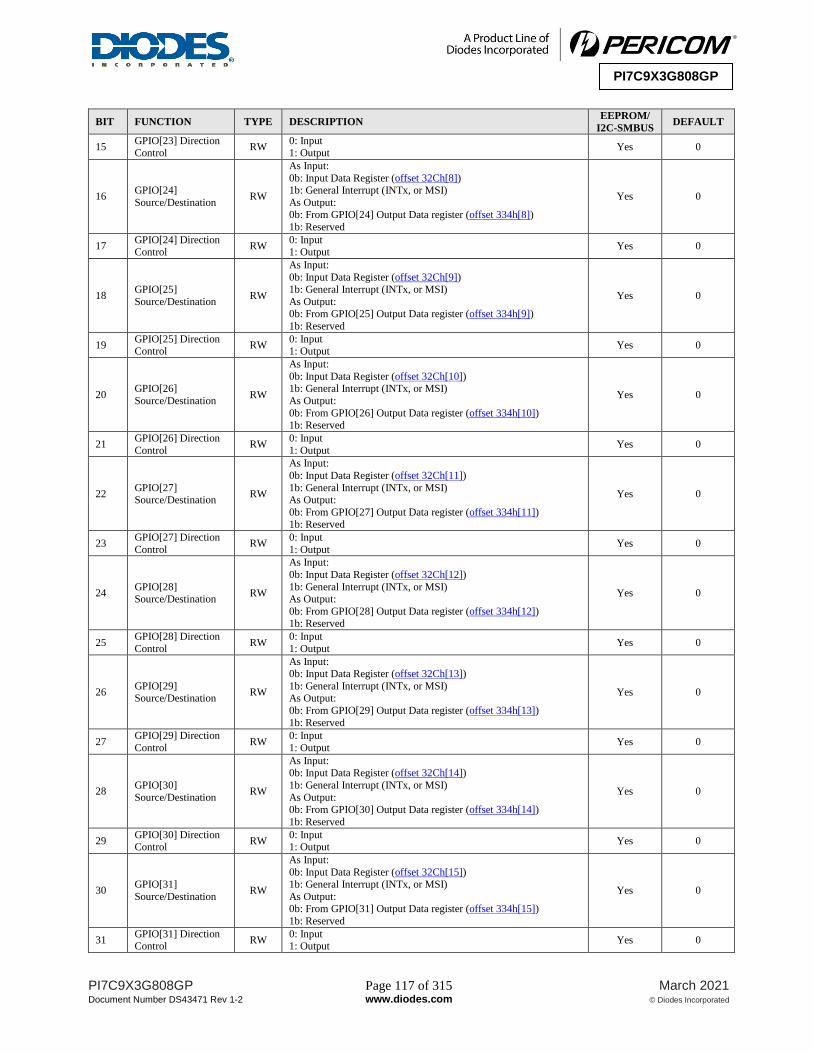
PI7C9X3G808GP Page 117 of 315 March 2021
Document Number DS43471 Rev 1-2 www.diodes.com © Diodes Incorporated
PI7C9X3G808GP
BIT FUNCTION TYPE DESCRIPTION EEPROM/
I2C-SMBUS DEFAULT
15 GPIO[23] Direction Control
RW 0: Input 1: Output
Yes 0
16 GPIO[24]
Source/Destination RW
As Input:
0b: Input Data Register (offset 32Ch[8]) 1b: General Interrupt (INTx, or MSI)
As Output: 0b: From GPIO[24] Output Data register (offset 334h[8])
1b: Reserved
Yes 0
17 GPIO[24] Direction Control
RW 0: Input 1: Output
Yes 0
18 GPIO[25]
Source/Destination RW
As Input:
0b: Input Data Register (offset 32Ch[9])
1b: General Interrupt (INTx, or MSI)
As Output: 0b: From GPIO[25] Output Data register (offset 334h[9])
1b: Reserved
Yes 0
19 GPIO[25] Direction Control
RW 0: Input 1: Output
Yes 0
20 GPIO[26]
Source/Destination RW
As Input:
0b: Input Data Register (offset 32Ch[10]) 1b: General Interrupt (INTx, or MSI)
As Output:
0b: From GPIO[26] Output Data register (offset 334h[10]) 1b: Reserved
Yes 0
21 GPIO[26] Direction
Control RW
0: Input
1: Output Yes 0
22 GPIO[27] Source/Destination
RW
As Input:
0b: Input Data Register (offset 32Ch[11])
1b: General Interrupt (INTx, or MSI) As Output:
0b: From GPIO[27] Output Data register (offset 334h[11]) 1b: Reserved
Yes 0
23 GPIO[27] Direction
Control RW
0: Input
1: Output Yes 0
24 GPIO[28] Source/Destination
RW
As Input:
0b: Input Data Register (offset 32Ch[12])
1b: General Interrupt (INTx, or MSI) As Output:
0b: From GPIO[28] Output Data register (offset 334h[12]) 1b: Reserved
Yes 0
25 GPIO[28] Direction
Control RW
0: Input
1: Output Yes 0
26 GPIO[29] Source/Destination
RW
As Input: 0b: Input Data Register (offset 32Ch[13])
1b: General Interrupt (INTx, or MSI) As Output:
0b: From GPIO[29] Output Data register (offset 334h[13])
1b: Reserved
Yes 0
27 GPIO[29] Direction
Control RW
0: Input
1: Output Yes 0
28 GPIO[30]
Source/Destination RW
As Input: 0b: Input Data Register (offset 32Ch[14])
1b: General Interrupt (INTx, or MSI)
As Output: 0b: From GPIO[30] Output Data register (offset 334h[14])
1b: Reserved
Yes 0
29 GPIO[30] Direction Control
RW 0: Input 1: Output
Yes 0
30 GPIO[31]
Source/Destination RW
As Input:
0b: Input Data Register (offset 32Ch[15])
1b: General Interrupt (INTx, or MSI)
As Output: 0b: From GPIO[31] Output Data register (offset 334h[15])
1b: Reserved
Yes 0
31 GPIO[31] Direction Control
RW 0: Input 1: Output
Yes 0

PI7C9X3G808GP Page 118 of 315 March 2021
Document Number DS43471 Rev 1-2 www.diodes.com © Diodes Incorporated
PI7C9X3G808GP
9.3.130 GPIO INPUT DE-BOUNCE REGISTER – OFFSET 324h (Port 0 Only)
BIT FUNCTION TYPE DESCRIPTION EEPROM/
I2C-SMBUS DEFAULT
31:0 GPIOx Input De-
Bounce Control RW
Controls de-bounce when the corresponding GPIOx signal is
configured as an input. Bit[31:0] correspond to GPIO[31:0], respectively.
0b: GPIOx input is not de-bounced
1b: GPIOx input is de-bounced
Yes 0000_0000h
9.3.131 GPIO 0-15 INPUT DATA REGISTER – OFFSET 328h (Port 0 Only)
BIT FUNCTION TYPE DESCRIPTION EEPROM/
I2C-SMBUS DEFAULT
0 GPIO[0] Input Data RO
GPIO[0] Input Data Return 0 if GPIO[0] is configured as an output (offset 31Ch[1]=1)
Return the state of GPIO[0] pin if GPIO[0] is configured as an input
(offset 31Ch[1]=0)
No 1
1 GPIO[1] Input Data RO
GPIO[1] Input Data
Return 0 if GPIO[1] is configured as an output (offset 31Ch[3]=1)
Return the state of GPIO[1] pin if GPIO[1] is configured as an input (offset 31Ch[3]=0)
No 1
2 GPIO[2] Input Data RO
GPIO[2] Input Data
Return 0 if GPIO[2] is configured as an output (offset 31Ch[5]=1) Return the state of GPIO[2] pin if GPIO[2] is configured as an input
(offset 31Ch[5]=0)
No 1
3 GPIO[3] Input Data RO
GPIO[3] Input Data Return 0 if GPIO[3] is configured as an output (ooffset 31Ch[7]=1)
Return the state of GPIO[3] pin if GPIO[3] is configured as an input (offset 31Ch[7]=0)
No 1
4 GPIO[4] Input Data RO
GPIO[4] Input Data
Return 0 if GPIO[4] is configured as an output (offset 31Ch[9]=1) Return the state of GPIO[4] pin if GPIO[4] is configured as an input
(offset 31Ch[9]=0)
No 1
5 GPIO[5] Input Data RO
GPIO[5] Input Data Return 0 if GPIO[5] is configured as an output (offset 31Ch[11]=1)
Return the state of GPIO[5] pin if GPIO[5] is configured as an input
(offset 31Ch[11]=0)
No 1
6 GPIO[6] Input Data RO
GPIO[6] Input Data
Return 0 if GPIO[6] is configured as an output (offset 31Ch[13]=1) Return the state of GPIO[6] pin if GPIO[6] is configured as an input
(offset 31Ch[13]=0)
No 1
7 GPIO[7] Input Data RO
GPIO[7] Input Data Return 0 if GPIO[7] is configured as an output (offset 31Ch[15]=1)
Return the state of GPIO[7] pin if GPIO[7] is configured as an input
(offset 31Ch[15]=0)
No 1
8 GPIO[8] Input Data RO
GPIO[8] Input Data
Return 0 if GPIO[8] is configured as an output (offset 31Ch[17]=1)
Return the state of GPIO[8] pin if GPIO[8] is configured as an input (offset 31Ch[17]=0)
No 1
9 GPIO[9] Input Data RO
GPIO[9] Input Data
Return 0 if GPIO[9] is configured as an output (offset 31Ch[19]=1) Return the state of GPIO[9] pin if GPIO[9] is configured as an input
(offset 31Ch[19]=0)
No 1
10 GPIO[10] Input Data RO
GPIO[10] Input Data Return 0 if GPIO[10] is configured as an output (offset
31Ch[21]=1) Return the state of GPIO[10] pin if GPIO[10] is configured as an
input (offset 31Ch[21]=0)
No 1
11 GPIO[11] Input Data RO
GPIO[11] Input Data Return 0 if GPIO[11] is configured as an output (offset
31Ch[23]=1)
Return the state of GPIO[11] pin if GPIO[11] is configured as an input (offset 31Ch[23]=0)
No 1

PI7C9X3G808GP Page 119 of 315 March 2021
Document Number DS43471 Rev 1-2 www.diodes.com © Diodes Incorporated
PI7C9X3G808GP
BIT FUNCTION TYPE DESCRIPTION EEPROM/
I2C-SMBUS DEFAULT
12 GPIO[12] Input Data RO
GPIO[12] Input Data Return 0 if GPIO[12] is configured as an output (offset
31Ch[25]=1) Return the state of GPIO[12] pin if GPIO[12] is configured as an
input (offset 31Ch[25]=0)
No 1
13 GPIO[13] Input Data RO
GPIO[13] Input Data Return 0 if GPIO[13] is configured as an output (offset
31Ch[27]=1)
Return the state of GPIO[13] pin if GPIO[13] is configured as an input (offset 31Ch[27]=0)
No 1
14 GPIO[14] Input Data RO
GPIO[14] Input Data Return 0 if GPIO[14] is configured as an output (offset
31Ch[29]=1)
Return the state of GPIO[11] pin if GPIO[11] is configured as an input (offset 31Ch[29]=0)
No 1
15 GPIO[15] Input Data RO
GPIO[15] Input Data
Return 0 if GPIO[15] is configured as an output (offset 31Ch[31]=1)
Return the state of GPIO[15] pin if GPIO[15] is configured as an input (offset 31Ch[31]=0)
No 1
31:16 Reserved RsvdP Not support. No 0000h
9.3.132 GPIO 16-31 INPUT DATA REGISTER – OFFSET 32Ch (Port 0 Only)
BIT FUNCTION TYPE DESCRIPTION EEPROM/
I2C-SMBUS DEFAULT
0 GPIO[16] Input Data RO
GPIO[16] Input Data
Return 0 if GPIO[16] is configured as an output (offset 320h[1]=1) Return the state of GPIO[16] pin if GPIO[16] is configured as an
input (offset 320h[1]=0)
Yes 1
1 GPIO[17] Input Data RO
GPIO[17] Input Data Return 0 if GPIO[17] is configured as an output (offset 320h[3]=1)
Return the state of GPIO[17] pin if GPIO[17] is configured as an input (offset 320h[3]=0)
Yes 1
2 GPIO[18] Input Data RO
GPIO[18] Input Data
Return 0 if GPIO[18] is configured as an output (offset 320h[5]=1) Return the state of GPIO[18] pin if GPIO[18] is configured as an
input (offset 320h[5]=0)
Yes 1
3 GPIO[19] Input Data RO
GPIO[19] Input Data Return 0 if GPIO[19] is configured as an output (offset 320h[7]=1)
Return the state of GPIO[19] pin if GPIO[19] is configured as an
input (offset 320h[7]=0)
Yes 1
4 GPIO[20] Input Data RO
GPIO[20] Input Data
Return 0 if GPIO[20] is configured as an output (offset 320h[9]=1)
Return the state of GPIO[20] pin if GPIO[20] is configured as an input (offset 320h[9]=0)
Yes 1
5 GPIO[21] Input Data RO
GPIO[21] Input Data Return 0 if GPIO[21] is configured as an output (offset 320h[11]=1)
Return the state of GPIO[21] pin if GPIO[21] is configured as an
input (offset 320h[11]=0)
Yes 1
6 GPIO[22] Input Data RO
GPIO[22] Input Data
Return 0 if GPIO[22] is configured as an output (offset 320h[13]=1)
Return the state of GPIO[22] pin if GPIO[22] is configured as an input (offset 320h[13]=0)
Yes 1
7 GPIO[23] Input Data RO
GPIO[23] Input Data
Return 0 if GPIO[23] is configured as an output (offset 320h[15]=1) Return the state of GPIO[23] pin if GPIO[23] is configured as an
input (offset 320h[15]=0)
Yes 1
8 GPIO[24] Input Data RO
GPIO[24] Input Data
Return 0 if GPIO[24] is configured as an output (offset 320h[17]=1)
Return the state of GPIO[24] pin if GPIO[24] is configured as an input (offset 320h[17]=0)
Yes 1

PI7C9X3G808GP Page 120 of 315 March 2021
Document Number DS43471 Rev 1-2 www.diodes.com © Diodes Incorporated
PI7C9X3G808GP
BIT FUNCTION TYPE DESCRIPTION EEPROM/
I2C-SMBUS DEFAULT
9 GPIO[25] Input Data RO
GPIO[25] Input Data Return 0 if GPIO[25] is configured as an output (offset 320h[19]=1)
Return the state of GPIO[25] pin if GPIO[25] is configured as an input (offset 320h[19]=0)
Yes 1
10 GPIO[26] Input Data RO
GPIO[26] Input Data
Return 0 if GPIO[26] is configured as an output (offset 320h[21]=1) Return the state of GPIO[26] pin if GPIO[26] is configured as an
input (offset 320h[21]=0)
Yes 1
11 GPIO[27] Input Data RO
GPIO[27] Input Data Return 0 if GPIO[27] is configured as an output (offset 320h[23]=1)
Return the state of GPIO[27] pin if GPIO[27] is configured as an input (offset 320h[23]=0)
Yes 1
12 GPIO[28] Input Data RO
GPIO[28] Input Data
Return 0 if GPIO[28] is configured as an output (offset 320h[25]=1) Return the state of GPIO[28] pin if GPIO[28] is configured as an
input (offset 320h[25]=0)
Yes 1
13 GPIO[29] Input Data RO
GPIO[29] Input Data Return 0 if GPIO[29] is configured as an output (offset 320h[27]=1)
Return the state of GPIO[29] pin if GPIO[29] is configured as an
input (offset 320h[27]=0)
Yes 1
14 GPIO[30] Input Data RO
GPIO[30] Input Data
Return 0 if GPIO[30] is configured as an output (offset 320h[29]=1)
Return the state of GPIO[30] pin if GPIO[30] is configured as an input (offset 320h[29]=0)
Yes 1
15 GPIO[31] Input Data RO
GPIO[31] Input Data
Return 0 if GPIO[31] is configured as an output (offset 320h[31]=1) Return the state of GPIO[31] pin if GPIO[31] is configured as an
input (offset 320h[31]=0)
Yes 1
31:16 Reserved RsvdP Not support. Yes 0000h
9.3.133 GPIO 0-15 OUTPUT DATA REGISTER – OFFSET 330h (Port 0 Only)
BIT FUNCTION TYPE DESCRIPTION EEPROM/
I2C-SMBUS DEFAULT
0 GPIO[0] Output Data RW
GPIO[0] Output Data
The value written to this bit is driven to GPIO[0] output if GPIO[0]
is configured as an output (offset 31Ch[1]=1)
Yes 0
1 GPIO[1] Output Data RW
GPIO[1] Output Data
The value written to this bit is driven to GPIO[1] output if GPIO[1]
is configured as an output (offset 31Ch[3]=1)
Yes 0
2 GPIO[2] Output Data RW
GPIO[2] Output Data
The value written to this bit is driven to GPIO[2] output if GPIO[2] is configured as an output (offset 31Ch[5]=1)
Yes 0
3 GPIO[3] Output Data RW
GPIO[3] Output Data
The value written to this bit is driven to GPIO[3] output if GPIO[3] is configured as an output (offset 31Ch[7]=1)
Yes 0
4 GPIO[4] Output Data RW
GPIO[4] Output Data
The value written to this bit is driven to GPIO[4] output if GPIO[4] is configured as an output (offset 31Ch[9]=1)
Yes 0
5 GPIO[5] Output Data RW
GPIO[5] Output Data
The value written to this bit is driven to GPIO[5] output if GPIO[5] is configured as an output (offset 31Ch[11]=1)
Yes 0
6 GPIO[6] Output Data RW
GPIO[6] Output Data
The value written to this bit is driven to GPIO[6] output if GPIO[6] is configured as an output (offset 31Ch[13]=1)
Yes 0
7 GPIO[7] Output Data RW
GPIO[7] Output Data
The value written to this bit is driven to GPIO[7] output if GPIO[7] is configured as an output (offset 31Ch[15]=1)
Yes 0
8 GPIO[8] Output Data RW
GPIO[8] Output Data
The value written to this bit is driven to GPIO[8] output if GPIO[8] is configured as an output (offset 31Ch[17]=1)
Yes 0
9 GPIO[9] Output Data RW
GPIO[9] Output Data
The value written to this bit is driven to GPIO[9] output if GPIO[9] is configured as an output (offset 31Ch[19]=1)
Yes 0

PI7C9X3G808GP Page 121 of 315 March 2021
Document Number DS43471 Rev 1-2 www.diodes.com © Diodes Incorporated
PI7C9X3G808GP
BIT FUNCTION TYPE DESCRIPTION EEPROM/
I2C-SMBUS DEFAULT
10 GPIO[10] Output Data
RW GPIO[10] Output Data The value written to this bit is driven to GPIO[10] output if
GPIO[10] is configured as an output (offset 31Ch[21]=1)
Yes 0
11 GPIO[11] Output Data
RW GPIO[11] Output Data The value written to this bit is driven to GPIO[11] output if
GPIO[11] is configured as an output (offset 31Ch[23]=1)
Yes 0
12 GPIO[12] Output Data
RW
GPIO[12] Output Data
The value written to this bit is driven to GPIO[12] output if
GPIO[12] is configured as an output (offset 31Ch[25]=1)
Yes 0
13 GPIO[13] Output Data
RW
GPIO[13] Output Data
The value written to this bit is driven to GPIO[13] output if
GPIO[13] is configured as an output (offset 31Ch[27]=1)
Yes 0
14 GPIO[14] Output Data
RW
GPIO[14] Output Data
The value written to this bit is driven to GPIO[14] output if
GPIO[14] is configured as an output (offset 31Ch[29]=1)
Yes 0
15 GPIO[15] Output Data
RW
GPIO[15] Output Data
The value written to this bit is driven to GPIO[15] output if
GPIO[15] is configured as an output (offset 31Ch[31]=1)
Yes 0
31:16 Reserved RsvdP Not support. No 0000h
9.3.134 GPIO 16-31 OUTPUT DATA REGISTER – OFFSET 334h (Port 0 Only)
BIT FUNCTION TYPE DESCRIPTION EEPROM/
I2C-SMBUS DEFAULT
0 GPIO[16] Output
Data RW
GPIO[16] Output Data
The value written to this bit is driven to GPIO[16] output if GPIO[16] is configured as an output (offset 320h[1]=1)
Yes 0
1 GPIO[17] Output
Data RW
GPIO[17] Output Data
The value written to this bit is driven to GPIO[17] output if GPIO[17] is configured as an output (offset 320h[3]=1)
Yes 0
2 GPIO[18] Output
Data RW
GPIO[18] Output Data
The value written to this bit is driven to GPIO[18] output if GPIO[18] is configured as an output (offset 320h[5]=1)
Yes 0
3 GPIO[19] Output
Data RW
GPIO[19] Output Data
The value written to this bit is driven to GPIO[19] output if GPIO[19] is configured as an output (offset 320h[7]=1)
Yes 0
4 GPIO[20] Output
Data RW
GPIO[20] Output Data
The value written to this bit is driven to GPIO[20] output if GPIO[20] is configured as an output (offset 320h[9]=1)
Yes 0
5 GPIO[21] Output
Data RW
GPIO[21] Output Data
The value written to this bit is driven to GPIO[21] output if GPIO[21] is configured as an output (offset 320h[11]=1)
Yes 0
6 GPIO[22] Output
Data RW
GPIO[22] Output Data
The value written to this bit is driven to GPIO[22] output if GPIO[22] is configured as an output (offset 320h[13]=1)
Yes 0
7 GPIO[23] Output
Data RW
GPIO[23] Output Data
The value written to this bit is driven to GPIO[23] output if GPIO[23] is configured as an output (offset 320h[15]=1)
Yes 0
8 GPIO[24] Output
Data RW
GPIO[24] Output Data
The value written to this bit is driven to GPIO[24] output if GPIO[24] is configured as an output (offset 320h[17]=1)
Yes 0
9 GPIO[25] Output
Data RW
GPIO[25] Output Data The value written to this bit is driven to GPIO[25] output if
GPIO[25] is configured as an output (offset 320h[19]=1)
Yes 0
10 GPIO[26] Output
Data RW
GPIO[26] Output Data The value written to this bit is driven to GPIO[26] output if
GPIO[26] is configured as an output (offset 320h[21]=1)
Yes 0
11 GPIO[27] Output
Data RW
GPIO[27] Output Data
The value written to this bit is driven to GPIO[27] output if
GPIO[27] is configured as an output (offset 320h[23]=1)
Yes 0
12 GPIO[28] Output
Data RW
GPIO[28] Output Data The value written to this bit is driven to GPIO[28] output if
GPIO[28] is configured as an output (offset 320h[25]=1)
Yes 0

PI7C9X3G808GP Page 122 of 315 March 2021
Document Number DS43471 Rev 1-2 www.diodes.com © Diodes Incorporated
PI7C9X3G808GP
BIT FUNCTION TYPE DESCRIPTION EEPROM/
I2C-SMBUS DEFAULT
13 GPIO[29] Output Data
RW GPIO[29] Output Data The value written to this bit is driven to GPIO[29] output if
GPIO[29] is configured as an output (offset 320h[27]=1)
Yes 0
14 GPIO[30] Output Data
RW GPIO[30] Output Data The value written to this bit is driven to GPIO[30] output if
GPIO[30] is configured as an output (offset 320h[29]=1)
Yes 0
15 GPIO[31] Output Data
RW
GPIO[31] Output Data
The value written to this bit is driven to GPIO[31] output if
GPIO[31] is configured as an output (offset 320h[31]=1)
Yes 0
31:16 Reserved RsvdP Not support. No 0000h
9.3.135 GPIO 0-31 INTERRUPT POLARITY REGISTER – OFFSET 338h (Port 0 Only)
BIT FUNCTION TYPE DESCRIPTION EEPROM/
I2C-SMBUS DEFAULT
31:0 GPIO Interrupt
Polarity RW
Controls whether GPIO Interrupt input is Active-Low or Active-
High for the corresponding GPIOx signal. Bit[31:0] correspond to GPIO[31:0], respectively.
0b: GPIOx Interrupt input is Active-Low 1b: GPIOx Interrupt input is Active-High
Yes 0000_0000h
9.3.136 GPIO 0-31 INTERRUPT STATUS REGISTER – OFFSET 33Ch (Port 0 Only)
BIT FUNCTION TYPE DESCRIPTION EEPROM/
I2C-SMBUS DEFAULT
31:0 GPIO Interrupt
Status RO
Indicates whether GPIO interrupt are inactive or active for the
corresponding GPIOx signal. Bit[31:0] correspond to GPIO[31:0] respectively.
0b: GPIOx interrupt is inactive
1b: GPIOx interrupt is active
No 8000_0000h
9.3.137 GPIO 0-31 INTERRUPT MASK REGISTER – OFFSET 340h (Port 0 Only)
BIT FUNCTION TYPE DESCRIPTION EEPROM/
I2C-SMBUS DEFAULT
31:0 GPIO Interrupt Mask RW
Indicates whether GPIO interrupts are masked or not masked for the corresponding GPIOx signal. Bit[31:0] correspond to GPIO[31:0],
respectively.
0b: GPIOx interrupt is unmasked
1b: GPIOx interrupt is masked
Yes 0000_0000h
9.3.138 OPERATION MODE REGISTER – OFFSET 348h (Port 0 Only)
BIT FUNCTION TYPE DESCRIPTION EEPROM/
I2C-SMBUS DEFAULT
2:0 Reserved RsvdP Not support. No 000b
5:3 pkgsel RO Package Bonding option. No 000b
8:6 portcfg RO
Port/lane configuration settins. They are decided by the status of
PORTCFG[2:0] strap pins 001b: 2 x4 ports 010b: 1 x4, 2 x2 ports
011b: 4 x2 ports
100b: 1 x4, 4 x1 ports 101b: 8 x1 ports
Others: Reserved
No
Set by
PORTCFG
[2:0]

PI7C9X3G808GP Page 123 of 315 March 2021
Document Number DS43471 Rev 1-2 www.diodes.com © Diodes Incorporated
PI7C9X3G808GP
BIT FUNCTION TYPE DESCRIPTION EEPROM/
I2C-SMBUS DEFAULT
10:9 chipmode RO
Chip operation mode selection. They are decided by the status of CHIPMODE[1:0] strap pins.
00b: Normal mode
01b: iddq/mbist mode 10b: AC JTAG mode
11b: phy_mode
No 00b
12:11 Reserved RsvdP Not support. No 00b
13 ckmode RO
Reference clock modes. It is decided by the status of CKMODE
strap pin.
0b: base mode
1b: CDEP separate reference mode
No 0b
14 dma_mode RO 0b: disable DMA
1b: enable DMA No 0
20:15 upport_sel RO Upstream port selection. No 0000_00b
21 CDEP_mode RO 0b: disable CDEP 1b: enable CDEP
No 0
22 scan_tm RO 0b: normal mode
1b: scan mode No 0
23 hotplug_pin_en RO
It is decided by the status of HOT_PLUG_EN_L strap pin.
0b: GPIO[31:0] are GPIO pins 1b: GPIO[31:0] are used as hot plug pins
No 1
24 surprise_hp_en RO 0b: disable surprise hot-plug 1b: enable surprise hot-plug
No 0
25 ioe_40bit_en RO 0b: support 16 bit IOE
1b: support 40 bit IOE No 0
26 clkbuf_pd RO
It is decided by the status of CLKBUFPD_L strap pin.
0b: clock buffer is in normal mode 1b: clock buffer is in power down mode
No 1
27 pm_l1_1_en RO
It is decided by the status of PM_L11_EN_L strap pin.
0b: GPIO[15:8] are GPIO pins
1b: GPIO[15:8] are used as CLKREQ_L[7:0]
No Set by
PM_L11_EN_L
30:28 I2c/smaddr_out RO Indicate I2C/SMBUS address[2:0]. No Set by
I2C_ADDRESS
[2:0]
31 Reserved RO Not Support. No 1
9.3.139 CLOCK BUFFER CONTROL REGISTER – OFFSET 34Ch (Port 0 Only)
BIT FUNCTION TYPE DESCRIPTION EEPROM/
I2C-SMBUS DEFAULT
7:0 Clock OE Control RW 0b… disable clock output 1b… enable clock output
Yes FFh
8 Clock Power Down RW
Used to set CLKBUFPD_L strap pin.
0b… power on
1b… power down
Yes 0
9 Control Enable RW 0b… disable to use this register control clock buffer output
1b… enable to use this register control clock buffer output Yes 0
10 Clock Source Sel RW 0b… input clock buffer source is from differential clock pad 1b… input clock buffer source is from CMOS single end clock
source
Yes 0
23:11 Reserved RsvdP Not support. No 0_0h
31:24 Revision ID RO Revision id. No 00h
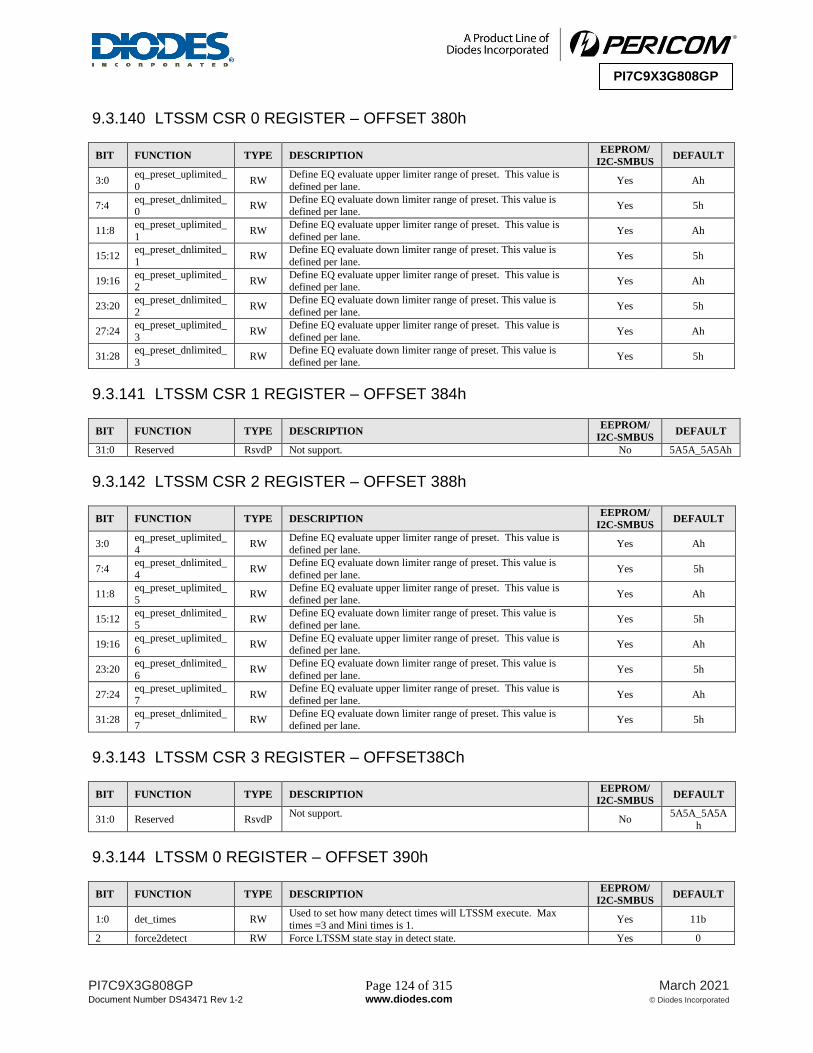
PI7C9X3G808GP Page 124 of 315 March 2021
Document Number DS43471 Rev 1-2 www.diodes.com © Diodes Incorporated
PI7C9X3G808GP
9.3.140 LTSSM CSR 0 REGISTER – OFFSET 380h
BIT FUNCTION TYPE DESCRIPTION EEPROM/
I2C-SMBUS DEFAULT
3:0 eq_preset_uplimited_
0 RW
Define EQ evaluate upper limiter range of preset. This value is
defined per lane. Yes Ah
7:4 eq_preset_dnlimited_0
RW Define EQ evaluate down limiter range of preset. This value is defined per lane.
Yes 5h
11:8 eq_preset_uplimited_
1 RW
Define EQ evaluate upper limiter range of preset. This value is
defined per lane. Yes Ah
15:12 eq_preset_dnlimited_
1 RW
Define EQ evaluate down limiter range of preset. This value is
defined per lane. Yes 5h
19:16 eq_preset_uplimited_
2 RW
Define EQ evaluate upper limiter range of preset. This value is
defined per lane. Yes Ah
23:20 eq_preset_dnlimited_
2 RW
Define EQ evaluate down limiter range of preset. This value is
defined per lane. Yes 5h
27:24 eq_preset_uplimited_
3 RW
Define EQ evaluate upper limiter range of preset. This value is
defined per lane. Yes Ah
31:28 eq_preset_dnlimited_3
RW Define EQ evaluate down limiter range of preset. This value is defined per lane.
Yes 5h
9.3.141 LTSSM CSR 1 REGISTER – OFFSET 384h
BIT FUNCTION TYPE DESCRIPTION EEPROM/
I2C-SMBUS DEFAULT
31:0 Reserved RsvdP Not support. No 5A5A_5A5Ah
9.3.142 LTSSM CSR 2 REGISTER – OFFSET 388h
BIT FUNCTION TYPE DESCRIPTION EEPROM/
I2C-SMBUS DEFAULT
3:0 eq_preset_uplimited_
4 RW
Define EQ evaluate upper limiter range of preset. This value is
defined per lane. Yes Ah
7:4 eq_preset_dnlimited_
4 RW
Define EQ evaluate down limiter range of preset. This value is
defined per lane. Yes 5h
11:8 eq_preset_uplimited_5
RW Define EQ evaluate upper limiter range of preset. This value is defined per lane.
Yes Ah
15:12 eq_preset_dnlimited_
5 RW
Define EQ evaluate down limiter range of preset. This value is
defined per lane. Yes 5h
19:16 eq_preset_uplimited_6
RW Define EQ evaluate upper limiter range of preset. This value is defined per lane.
Yes Ah
23:20 eq_preset_dnlimited_
6 RW
Define EQ evaluate down limiter range of preset. This value is
defined per lane. Yes 5h
27:24 eq_preset_uplimited_
7 RW
Define EQ evaluate upper limiter range of preset. This value is
defined per lane. Yes Ah
31:28 eq_preset_dnlimited_7
RW Define EQ evaluate down limiter range of preset. This value is defined per lane.
Yes 5h
9.3.143 LTSSM CSR 3 REGISTER – OFFSET38Ch
BIT FUNCTION TYPE DESCRIPTION EEPROM/
I2C-SMBUS DEFAULT
31:0 Reserved RsvdP Not support.
No 5A5A_5A5A
h
9.3.144 LTSSM 0 REGISTER – OFFSET 390h
BIT FUNCTION TYPE DESCRIPTION EEPROM/
I2C-SMBUS DEFAULT
1:0 det_times RW Used to set how many detect times will LTSSM execute. Max
times =3 and Mini times is 1. Yes 11b
2 force2detect RW Force LTSSM state stay in detect state. Yes 0
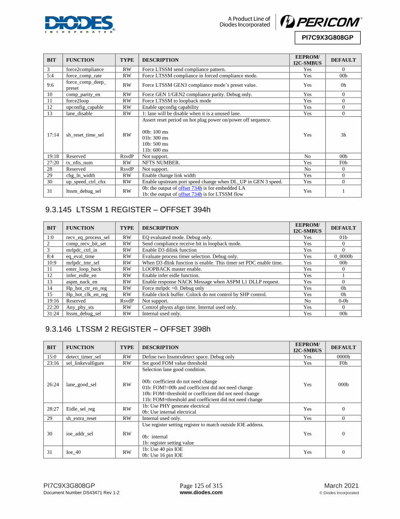
PI7C9X3G808GP Page 125 of 315 March 2021
Document Number DS43471 Rev 1-2 www.diodes.com © Diodes Incorporated
PI7C9X3G808GP
BIT FUNCTION TYPE DESCRIPTION EEPROM/
I2C-SMBUS DEFAULT
3 force2compliance RW Force LTSSM send compliance pattern. Yes 0
5:4 force_comp_rate RW Force LTSSM compliance in forced compliance mode. Yes 00b
9:6 force_comp_deep_
preset RW Force LTSSM GEN3 compliance mode’s preset value. Yes 0h
10 comp_parity_en RW Force GEN 1/GEN2 compliance parity. Debug only. Yes 0
11 force2loop RW Force LTSSM to loopback mode Yes 0
12 upconfig_capable RW Enable upconfig capability Yes 0
13 lane_disable RW 1: lane will be disable when it is a unused lane. Yes 0
17:14 sh_reset_time_sel RW
Assert reset period on hot plug power on/power off sequence.
00b: 100 ms 01b: 300 ms
10b: 500 ms
11b: 600 ms
Yes 3h
19:18 Reserved RsvdP Not support. No 00b
27:20 tx_nfts_num RW NFTS NUMBER. Yes F0h
28 Reserved RsvdP Not support. No 0
29 chg_ln_width RW Enable change link width Yes 0
30 up_speed_ctrl_chx RW Enable upstream port speed change when DL_UP in GEN 3 speed. Yes 0
31 ltssm_debug_sel RW 0b: the output of offset 734h is for embedded LA
1b: the output of offset 734h is for LTSSM flow Yes 1
9.3.145 LTSSM 1 REGISTER – OFFSET 394h
BIT FUNCTION TYPE DESCRIPTION EEPROM/
I2C-SMBUS DEFAULT
1:0 recv_eq_process_sel RW EQ evaluated mode. Debug only. Yes 01b
2 comp_recv_bit_set RW Send compliance receive bit in loopback mode. Yes 0
3 mrlpdc_ctrl_in RW Enable D3 dilink function Yes 0
8:4 eq_eval_time RW Evaluate process timer selection. Debug only. Yes 0_0000b
10:9 mrlpdc_tmr_sel RW When D3 dlink function is enable. This timer set PDC enable time. Yes 00b
11 enter_loop_back RW LOOPBACK master enable. Yes 0
12 infer_eidle_en RW Enable infer eidle function. Yes 1
13 aspm_nack_en RW Enable response NACK Message when ASPM L1 DLLP request. Yes 0
14 Hp_hot_ctr_en_reg RW Force mrlpdc =0. Debug only Yes 0h
15 Hp_hot_clk_en_reg RW Enable clock buffer. Colock do not control by SHP control. Yes 0h
19:16 Reserved RsvdP Not support. No 0-0b
22:20 Any_phy_sts RW Control physts align time. Internal used only. Yes 0
31:24 ltssm_debug_sel RW Internal used only. Yes 00h
9.3.146 LTSSM 2 REGISTER – OFFSET 398h
BIT FUNCTION TYPE DESCRIPTION EEPROM/
I2C-SMBUS DEFAULT
15:0 detect_timer_sel RW Define two ltssmtxdetect space. Debug only Yes 0000h
23:16 sel_linkevalfigure RW Set good FOM value threshold Yes F0h
26:24 lane_good_sel RW
Selection lane good condition.
00b: coefficient do not need change
01b: FOM!=00b and coefficient did not need change 10b: FOM=threshold or coefficient did not need change
11b: FOM=threshold and coefficient did not need change
Yes 000b
28:27 Eidle_sel_reg RW 1b: Use PHY generate electrical 0b: Use internal electrical
Yes 0
29 sh_extra_reset RW Internal used only. Yes 0
30 ioe_addr_sel RW
Use register setting register to match outside IOE address.
0b: internal
1b: register setting value
Yes 0
31 Ioe_40 RW 1b: Use 40 pin IOE 0b: Use 16 pin IOE
Yes 0

PI7C9X3G808GP Page 126 of 315 March 2021
Document Number DS43471 Rev 1-2 www.diodes.com © Diodes Incorporated
PI7C9X3G808GP
9.3.147 LTSSM 3 REGISTER – OFFSET 39Ch
BIT FUNCTION TYPE DESCRIPTION EEPROM/
I2C-SMBUS DEFAULT
6:0 cfg_address_in RW IOE address defined by register. Yes 00h
7 hp_scl_clk_sel_in RW
I2C clock rate.
0b: 62Khz
1b: 31Khz
Yes 0
15:8 aspm_l1_cnt_num RW Accumulated l0s number to enter ASPM L1 condition. Yes 08h
31:16 aspm_l1 RW ASPM L1 idle timer. Yes 0FFFh
9.3.148 LTSSM 4 REGISTER – OFFSET 3A0h
BIT FUNCTION TYPE DESCRIPTION EEPROM/
I2C-SMBUS DEFAULT
15:0 tx_swing RW TX swing setting by register value. Yes 0000h
17:16 Eios_cnt RW Polling compliance exit condition. Yes 1
18 Bypass_detect RW Ignore LTSSM detect result and use max lane width. Yes 0
19 Detection_option RW 1b: use detection result
0b: use modify detection result Yes 0
20 Stand_by RW
Used to control whether the PHY rx is active when PHY is in P0 or P0s.
1b: Active 0b: Standby
Yes 0
21 In_progress RW Set rxeqprocess behavior. Internal used only. Yes 0
22 Deskew_rxeqval RW Set deskew behavior in EQ period. Internal used only. Yes 0
23 Ltssm_cfg2loop_sel RW
Cfg go to loopback condition.
0b : see any loopback bit 1b: see all loopback bit. Internal used only.
Yes 0
27:24 Recv_eq_optionl RW
Eq_option.
bit[0]… set eq_valid =1
Yes 001b
31:28 Ltssm_cfg_reversal RW Select reversal condition. Internal used only. Yes 0
9.3.149 LTSSM 5 REGISTER – OFFSET 3A4h
BIT FUNCTION TYPE DESCRIPTION EEPROM/
I2C-SMBUS DEFAULT
15:0 tskp_gen1_n0_reg RW When sris support, use this skip value. Yes 004Bh
31:16 skp_gen1_reg RW When sris disable, use the skip value. Yes 0258h
9.3.150 LTSSM 6 REGISTER – OFFSET 3A8h
BIT FUNCTION TYPE DESCRIPTION EEPROM/
I2C-SMBUS DEFAULT
15:0 tskp_gen3_n0_reg RW When sris support, use this skip value. Yes 011Ch
31:16 tskp_gen3_reg RW When sris disable, use the skip value. Yes 0BBEh
9.3.151 LTSSM 7 REGISTER – OFFSET 3ACh
BIT FUNCTION TYPE DESCRIPTION EEPROM/
I2C-SMBUS DEFAULT
4:0 ltssm_rx_mask_reg RW
bit[0]… mask hot reset bit
bit[1]… mask disable bit bit[2]… mask loopback bit
bit[3]… mask disable scrambling bit bit[4]… mask compliance bit
Yes 0_0000b
5 ltssm_port_split_ctr_
reg RW
0b: enable port split
1b: disable port split Yes 0

PI7C9X3G808GP Page 127 of 315 March 2021
Document Number DS43471 Rev 1-2 www.diodes.com © Diodes Incorporated
PI7C9X3G808GP
BIT FUNCTION TYPE DESCRIPTION EEPROM/
I2C-SMBUS DEFAULT
9:6 ltssm_lg_idle_cnt_ reg
RW Used to set idle data receive date number. Yes 6h
10 ltssm_chg_rate_ms_
reg RW Used to control down port change rate as a master. Yes 0
11 gpio_in_reg_tmp RW In external I2C IOE bit[6],it is GPIO bit. Yes 0
15:12 ltssm_config_rev_
num_reg RW
bit[1:0]… cfg.linkaccept to cfg.linkwait couter selection.
bit[3:2]… cfg.lanenum to cfg.cpl counter selection Yes 0000b
16 ltssm_config_delay_
cnt_reg RW
cfg.start delay time to cfg.linkaccept. Use this delay time to decide
partial lane detection. Yes 0
17 disable_cfg_lane_ chg_reg
RW disable cfg.linkaccept state change lane. Yes 0
18 disable_cfg_lane_
time_reg RW disable cfg.lanenum to detect state. Yes 0
22:19 partial_lane_sel_reg RW bit[1:0]… decide partial lane reverse bit[2]… Reserved
bit[3]… delay cfg.start to cfg.linaccept sate for cross link
Yes 0001b
23 enable_becon_l2_reg RW Used to enable L2 send becon signal. Yes 0
24 Reserved RsvdP Not support. No 0
26:25 lane_change_ctr_reg RW Used to control lane number change in cfg state. Yes 00b
28:27 poll_exit_comp_cnt_reg
RW Used to set poll.compliance exit counter. Yes 11b
29 led_mode_prsnt_sel_
reg RW
Used to select present detect pin come from IOE or IO pin in
surprise mode. Yes 1
30 shp_rest_ctr_reg RW
Used to control ip_core reset pin come from reset_top or shp generation.
0b: come from shp generation
1b: come from reset_top
Yes 0
31 always_wait_linkup_reg
RW In shp control, shp try to link up device always. Yes 0
9.3.152 LTSSM 8 REGISTER – OFFSET 3B0h
BIT FUNCTION TYPE DESCRIPTION EEPROM/
I2C-SMBUS DEFAULT
0 dpc_error_latch RW
When dpc error occurs, ltssm will entry to disable state.
0b: dpc error signal will be latched until ltssm go to disable state.
1b: dpc error signal will not be latched.
Yes 1
1 any_phy_sts_tmp_sel_reg
RW 0b: come from all phy_sts 1b: combine with lane detetion.
Yes 0
5:2 cfg_stat_ctr_reg RW cfg_start option selection. Yes 0000b
19:6 rate_chg_ctr_reg RW Used to control rate change behavior. Yes 0-0b
23:20 loop_test_ctr_reg RW loop test behavior control. Yes 0h
25:24 l0_power_dn_wait_ reg
RW
When receive/transmitter eios, pm control wait 50 cycle time to
L1/l0s/L2.
00b: 50
01b: 1Fh 10b: FFh
11b: FFFFh
Yes 00b
26 gen3_phy_pm_eidle_control_reg
RW 0b: use rxeidle in PM 1b: ignore rxeidle in PM
Yes 0
27 eq1to0_eval_reg RW 0b: disble skip eq23
1b: skip eq23 Yes 0
30:28 debunce_sel_reg RW
bit[1:0]… attention button/present detection de-bounce timer.
00b: C00h
01b: FFFh
10b: 600h
11b: 0FFh bit[2]… de-bounce enable
Yes 100b
31 Reserved RsvdP Not support No 0

PI7C9X3G808GP Page 128 of 315 March 2021
Document Number DS43471 Rev 1-2 www.diodes.com © Diodes Incorporated
PI7C9X3G808GP
9.3.153 LTSSM 9 REGISTER – OFFSET 3B4h
BIT FUNCTION TYPE DESCRIPTION EEPROM/
I2C-SMBUS DEFAULT
0 clear_rx_sts_err_
counter WO
Reading returns 0 always. Writing 1 will celar rx status error
counter. Yes 0
1 redo_eq_ctrl RW 1b: redo eq when rx error > static_counter set by bit[15:8] in GEN3 Yes 0
2 static_enable_reg RW 1b: enable perform downstream port eq when error Yes 0
3 perform_eq_
err_reg RW
1b: when rx error occurred enable to perform redo eq
0b: disable Yes 0
4 static_enable_up_reg RW 1b: enable up port execute eq when rx error count > static_counter set by bit[15:8]
Yes 0
7:5 Reserved RsvdP Not support. No 000b
15:8 static_ctrl_sel_num RW Used to set static_counter. Yes 01h
31:16 rx_sts_err_counter RO Reading returns rx status error counter value. Writing this register
will result in undefined behavior. No 0000h
9.3.154 LTSSM 10 REGISTER – OFFSET 3B8h
BIT FUNCTION TYPE DESCRIPTION EEPROM/
I2C-SMBUS DEFAULT
19:0 CLKREQ_L Wait
Time RW
Once entering L1.1 power state, the port will deassert CLKREQ_L immediately.
However, CLKREQ_L signal is an open-drain wire-or signal with
the link partner. If the link partner does not deassert CLKREQ_L for a certain period
of time, which is defined by CLKREQ_L Wait Time, the port will assert CLKREQ_L again to resume back
to L1 state.
The CLKREQ_L wait time decides how long the switch will wait
for CLKREQ_L being deasserted by the link partner. The unit is “10 ns”.
Reset to F_FF00h. It is about 10 ms.
Yes F_FF00h
20 up_entry_l1.1 RW 0b: enable up port can entry to L1.1 Yes 0
21 dn_entry_l1.1 RW 0b: enable down port can entry to L1.1 Yes 0
31:22 Reserved RsvdP Not support. No 000h
9.3.155 LTSSM 11 REGISTER – OFFSET 3BCh
BIT FUNCTION TYPE DESCRIPTION EEPROM/
I2C-SMBUS DEFAULT
0 hp_scl_clk_sel_in_ dly_tmp
RW Used to set hp_i2c delay counter. Yes 0
2:1 recv_tor_ts12_num_
reg RW
Used to set receive change bit number that fire rec.cfg change to
rec.speed. Yes 10b
3 poll_exit_comp_cnt_sel_reg
RW Used to control poll.compliance exit. Yes 0
6:4 loop_test_ctr_eios_ reg
RW Used to set receive eios number in loop.exit state. Yes 010b
7 shp_command_dis_
em_reg RW
Used to check electromechanical control combine with set slot
command. Yes 0
15:8 pm_phy_rxeidle_cnt_sel_reg
RW Used to control Pm phy rxeidle counter. Yes 01h
31:16 cfg_cnt_ctr_reg RW Used to control ltssm cfg state. Yes 9C49h
9.3.156 LTSSM 12 REGISTER – OFFSET 3C0h
BIT FUNCTION TYPE DESCRIPTION EEPROM/
I2C-SMBUS DEFAULT
0 dis_ini_hw_dis RW 0b: disable hardware autonomous speed bit in link control 2 register 1b: enable
Yes 0

PI7C9X3G808GP Page 129 of 315 March 2021
Document Number DS43471 Rev 1-2 www.diodes.com © Diodes Incorporated
PI7C9X3G808GP
BIT FUNCTION TYPE DESCRIPTION EEPROM/
I2C-SMBUS DEFAULT
1 up_hot_reset RW 0b: upstream port does not send hot reset go through recovery 1b: upstream port send hot reset go through recovery
Yes 0
2 rev_ext RW When enable it,pm will check recovery state and pm sate is 0 then
exit to l0. Yes 0
3 rev_ext1 RW When enable it ,ltssm check rxeidle in ltssm l1 state. If rxeidle is
low,ltssm l1 will jump to l0. Yes 0
7:4 par_eidle_sel RW
bit[0]: when set, ignore fts packet to generate gen3 rxeidle. bit[1]: when set, ignore ts1 packet to generate gen3 rxeidle.
bit[2]: when set, ignore ts2 packet to generate gen3 rxeidle. bit[3]: when set, ignore eios packet to generate gen3 rxeidle.
Yes 1000b
15:8 l1_rev_ext1_cnt RW When wire l1_rev_ext1_reg is enabled, the counter use to evaluate
high for rxeidle. Yes 1Fh
23:16 pm_phy_rxeidle_cnt_sel1_reg
RW Stay in l1 counter; l1 to l0 counter. It make sure all conditions are meet. It is used for test mode only.
Yes 06h
24 ack_nak_empty_o_
reg RW
0b: check ack or nack is empty when l0 to l1.
1b: do not check ack or nack is empty when l0 to l1. Yes 0
25 eq_start_ctrl_reg RW 0b: get coefficient do not check whether state in eq state.
1b: get coefficient check whether state in eq state. Yes 0
26 dis_change_rate_ coef_reg
RW 0b: enable change lane width change function. 1b: disable lane width change function.
Yes 0
28:27 eios_ctrl_reg_0 RW Used to check receive eios counter in change rate stage. Yes 00b
31:29 eios_ctrl_reg_1 RW Used to send eios number in change rate. Yes 100b
9.3.157 LTSSM 13 REGISTER – OFFSET 3C4h
BIT FUNCTION TYPE DESCRIPTION EEPROM/
I2C-SMBUS DEFAULT
7:0 transmit idle data number[7:0]
RW Used to set transmit idle data number. Yes 08h
11:8 receive idle data[3:0] RW Used to set receive idle data. Yes 8h
12 disable_pol2loop_reg RW 1b: enable pol2loop 0b: disable pol2loop
Yes 0
14:13 Reserved RsvdP Not support. No 10b
15 Forced to Gen 3 RW
Forced the downstream port trying to link at Gen 3 speed if the link
partner reporting Gen 3 link capability.
0b: No trying (i.e. linked at whatever speed per standard flow) 1b: Keep trying to change rate to Gen 3 until success
Yes 0
23:16 cfg_ctrl_sub_reg
[7:0] RW Used to set cfg_ctrl_sub register. Yes 06h
25:24 rate_eq_ctr2_reg
[1:0] RW Used to set rate_eq_ctr2 register. Yes 00b
29:26 eq_done_8g_ctr_ reg[3:0]
RW Used to set eq_done_8g_ctrl register. Yes 0110b
31:30 up_have_rcv_eq1_
reg[1:0] RW Used to set up_have_rcv_eq1 register. Yes 00b
9.3.158 LTSSM 14 REGISTER – OFFSET 3C8h
BIT FUNCTION TYPE DESCRIPTION EEPROM/
I2C-SMBUS DEFAULT
3:0 lane_sel_cnt RW Select lane preset which eq negotiate result. Yes 0h
7:4 sphp_ctrl_reg RW Serial hot plug controller for power control option 0. Yes 0h
9:8 pme_to_ack_timer_
reg RW Pme to ack response timer selection. Yes 00b
10 send_pack_on_time_
reg RW Send link up/all port enter eidle message to main tie at fixed time. Yes 0
19:11 disable_eios_reg RW Pm eidle option. Yes 0-0b
20 diable_hot_reset_reg RW 0b: hotreset state send ts1 after sds send at recovery state 1b: hotreset state send ts1 directly
Yes 0
23:21 recovery_idle_count RW Used to configure recovery idle send amount of additional idle
symbol number. Yes 000b
27:24 eq_number_ask RO EQ number that DUT ask number to link partner. No 0h

PI7C9X3G808GP Page 130 of 315 March 2021
Document Number DS43471 Rev 1-2 www.diodes.com © Diodes Incorporated
PI7C9X3G808GP
BIT FUNCTION TYPE DESCRIPTION EEPROM/
I2C-SMBUS DEFAULT
31:28 eq_number_applied RO EQ number that come from link partner. No 0h
9.3.159 LTSSM 15 REGISTER – OFFSET 3CCh
BIT FUNCTION TYPE DESCRIPTION EEPROM/
I2C-SMBUS DEFAULT
0 pwr_det_ctrl RW
Used to enable power saing function at empty port.
0b: disable power saving function at empty port 1b: enable power saving function at empty port
Yes 0
1 recovery_ctrl RW When set 1, entry to recovery will ignore rx is in l0s. Yes 0
2 fake_oder_set_done RW When set 1, ltssm will auto generate order set done sinal when ltssm set pipe_tx_os signal large than ff cycle time.
Yes 0
3 disable_skip_at_l0 RW When set 1, send skip signal will extend until send skip packet
done. Yes 0
7:4 disable_reject RW Used to control reject bit behavior on ts order set at eq process. Yes 0h
23:8 comp_ctrl_gen1/2 WO Used to control compliance pattern behavior on gen1/gen2. Yes 0000h
31:24 Reserved RsvdP Not support. No 00h
9.3.160 DLL CSR 0 REGISTER – OFFSET 420h
BIT FUNCTION TYPE DESCRIPTION EEPROM/
I2C-SMBUS DEFAULT
11:0 GEN1_ACK_ LATENCY_CTRL
RW bit[11]: user enable bit[10:0]: user define ACK latency value
Yes 800h
15:12 Reserved RsvdP Not support. No 0h
16 BLOCK_BUMP_ DET
RO Block list has been overrun. No 0
27:17 Reserved RsvdP Not support. No 0_0b
28 TLP_NO_EOF_ERR
_DFT RO Detecting TLP has no end of frame. No 0
29 TLP_HEADER_
ERR_DET RO Detecting header of TLP is wrong. No 0
30 FIFO_LTH_ERR_ABORT_DET
RO Detecting total length of TLP is abort. No 0
31 FIFO_LTH_ERR_
DET RO Detecting total length of TLP is wrong. No 0
9.3.161 DLL CSR 1 REGISTER – OFFSET 424h
BIT FUNCTION TYPE DESCRIPTION EEPROM/
I2C-SMBUS DEFAULT
11:0 GEN2_ACK_ LATENCY_CTRL
RW Bit[11]: user enable Bit[10:0]: user define ACK latency value
Yes 800h
15:12 Reserved RsvdP Not support. No 0h
16 BLOCK_BUMP_ DET
RO Block list has been overrun. No 0
27:17 Reserved RsvdP Not support. No 0_0b
28 TLP_NO_EOF_ERR_DFT
RO Detecting TLP has no end of frame. No 0
29 TLP_HEADER_
ERR_DET RO Detecting header of TLP is wrong. No 0
30 FIFO_LTH_ERR_ABORT_DET
RO Detecting total length of TLP is abort. No 0
31 FIFO_LTH_ERR_
DET RO Detecting total length of TLP is wrong. No 0

PI7C9X3G808GP Page 131 of 315 March 2021
Document Number DS43471 Rev 1-2 www.diodes.com © Diodes Incorporated
PI7C9X3G808GP
9.3.162 DLL CSR 2 REGISTER – OFFSET 428h
BIT FUNCTION TYPE DESCRIPTION EEPROM/
I2C-SMBUS DEFAULT
11:0 GEN3_ACK_
LATENCY_CTRL RW
bit[11]: user enable
bit[10:0]: user define ACK latency value Yes 800h
15:12 Reserved RsvdP Not support. No 0h
16 BLOCK_BUMP_
DET RO Block list has been overrun. No 0
27:17 Reserved RsvdP Not support. No 0_0b
28 TLP_NO_EOF_ERR_DFT
RO Detecting TLP has no end of frame. No 0
29 TLP_HEADER_
ERR_DET RO Detecting header of TLP is wrong. No 0
30 FIFO_LTH_ERR_A
BORT_DET RO Detecting total length of TLP is abort. No 0
31 FIFO_LTH_ERR_ DET
RO Detecting total length of TLP is wrong. No 0
9.3.163 DLL CSR 3 REGISTER – OFFSET 42Ch
BIT FUNCTION TYPE DESCRIPTION EEPROM/
I2C-SMBUS DEFAULT
11:0 GEN1_REPLAY_
TIMER_CTRL RW User defined replay timeout value for GEN1. Yes 000h
12 User_define_GEN1_
REPLAY_TIMER RW
0b: disable user defined replay timer for GEN1
1b: enable user defined replay timer for GEN1 Yes 0b
21:13 retry buffer threshold
for 128 RW Used to set retry buffer threshould for 128 payload. Yes 1F1h
30:22 retry buffer threshold
for 256 RW Used to set retry buffer threshold for 256 payload. Yes 1F0h
31 tx ready non valid error by transaction
layer
RW1C For internal used. Yes 0
9.3.164 DLL CSR 4 REGISTER – OFFSET 430h
BIT FUNCTION TYPE DESCRIPTION EEPROM/
I2C-SMBUS DEFAULT
11:0 GEN2_REPLAY_ TIMER_CTRL
RW User defined replay timeout value for GEN2. Yes 000h
12 User_define_GEN2_
REPLAY_TIMER RW
0b: disable user defined replay timer for GEN2
1b: enable user defined replay timer for GEN2 Yes 0b
21:13 retry buffer threshold
for 512 RW Used to set retry buffer threshould for 512 payload. Yes 1E0h
23:22 External dlp_tx_block_ctrl
RW Internal used only. Yes 11b
31:24 Internal
dlp_tx_block_ctrl RW Internal used only Yes FBh
9.3.165 DLL CSR 5 REGISTER – OFFSET 434h
BIT FUNCTION TYPE DESCRIPTION EEPROM/
I2C-SMBUS DEFAULT
11:0 GEN3_REPLAY_
TIMER_CTRL RW User defined replay timeout value for GEN2 Yes 000h
12 User_define_GEN3_
REPLAY_TIMER RW
0b: disable user defined replay timer for GEN3
1b: enable user defined replay timer for GEN3 Yes 0b
13 reserved RO Not support No 0b
15:14 Loopback
synchronous signal RO Internal used only. No 0h
27:16 Loopback error count RW1C Only bit 16 write one to clear count. No 0h
29:28 DLP TX control RW Internal used only. Yes 01b

PI7C9X3G808GP Page 132 of 315 March 2021
Document Number DS43471 Rev 1-2 www.diodes.com © Diodes Incorporated
PI7C9X3G808GP
BIT FUNCTION TYPE DESCRIPTION EEPROM/
I2C-SMBUS DEFAULT
30 Loopback insert error RW User insert error to loopback Yes 0b
31 Loopback packet
start RW Start loopback packet. Yes 0b
9.3.166 DLL CSR 6 REGISTER – OFFSET 438h
BIT FUNCTION TYPE DESCRIPTION EEPROM/
I2C-SMBUS DEFAULT
6:0 INI_FLOW_CTRL RW
bit[2:0]: The value of firing initial flow control after getting flow control from frond end
bit[3]: user enable
bit[4]: enable to make initial flow control 1 transfer to initial flow control 2 early by getting any TLP or initial flow control 2
bit[5]: enable to make initial flow control 2 transfer to initial done by getting any TLP
bit[6]: enable to make initial flow control to initial done by getting
any good TLP or update flow control
Yes 70h
7 INI_FLOW2_EN RW Don’t need initial flow control 2. Yes 0
8 Dis_replaytimer_rx RW Used to disable Replay timer enable in RX L0s. Yes 1
9 Dis_replaytimer_tx RW Used to disable Replay timer enable in TX L0s. Yes 0
10 En_duplicate_seq_ nak
RW Used to enable duplicate sequence number for NAK. Yes 0
11 En_bypass_flowctrl RW Used to bypass initial flow control 1 to TL. Yes 1
12 Rx_polarity_force_ en
RW Used to enable RX polarity force. Yes 0
15:13 Reserved RsvdP Not support. No 000b
31:16 Rx_polarity_value RW Used to set rx polarity value for 16 lanes. Yes 0000h
9.3.167 DLL CSR 7 REGISTER – OFFSET 43Ch
BIT FUNCTION TYPE DESCRIPTION EEPROM/
I2C-SMBUS DEFAULT
8:0 DLL_DEBUG_SEL RW Data link layer debug select. Yes 0_0b
9 DLL Error Enable RW
Used to enable or disable DLL Error report to AER.
0b: disable 1b: enable
Yes 1
10 TLP Error Enable RW Used to enable or disable TLP Error report to AER. Yes 1
11 DLL Protocol Error
Enable_Disable RW
Used to enable or disable DLL Protocol Error report to AER.
0b: disable for P1~P7 and enable for P0 and P4
1b: enable for P1~P7 and disable for P0 and P4
Yes 1
12 Receive Error Enable RW
Used to enable or disable Receive Error to AER.
0b: disable 1b: enable
Yes 1
16:13 MAC ERR extend
control RW Internal used only. Yes 7h
18:17 EIOS amount control RW Internal used only. Yes 00b
24:19 DLL rx control RW Internal used only. Yes 7h
29:25 Reserved RsvdP Not support. No 0_0h
31:30 Loopback mode status
RO Indicate loopback mode status. No 00b

PI7C9X3G808GP Page 133 of 315 March 2021
Document Number DS43471 Rev 1-2 www.diodes.com © Diodes Incorporated
PI7C9X3G808GP
9.3.168 DLL CSR 8 REGISTER – OFFSET 440h
BIT FUNCTION TYPE DESCRIPTION EEPROM/
I2C-SMBUS DEFAULT
12:0 ERR_CTRL_500M RW
bit[0]: EIEOS error status enable
bit[1]: SKIP on data stream error status enable bit[2]: NFTS error status enable
bit[3]: SKIP framing error status enable
bit[4]: GEN3 logical idle error status enable bit[5]: EDS token to get FTS error status enable
bit[6]: GEN3 FCRC error status enable bit[7]: GEN3 EDB token error status enable
bit[8]: GEN3 TLP framing error status enable
bit[9]: TLP Framing check enable
bit[10]: GEN1/2 TLP framing error status error enable
bit[11]: GEN1/2 PAD framing error status enable bit[12]: GEN1/2 SDP framing error status enable
Yes 000h
13 GEN1/2_framing_err
_en RW GEN1/2 framing error enable. Yes 0
14 Recovery_enable_for_err_detect
RW Recovery enable for error detect. Yes 1
15 Recovery_for_replay
_rollover RW Replay rollover to recovery enable. Yes 1
16 GEN3_sync_header_
err_detect RW GEN3 synchronous header error detect. Yes 1
17 PHY_err_detect_en RW PHY status error detect enable. Yes 1
18 GEN3_skip_back2 back_err_detect
RW GEN3 SKIP back 2 back error detect. Yes 0
19 Elastic_buf_overrun_
detect RW Elastic buffer overrun detect. Yes 0
20 Elastic_buf_underrun
_detect RW Elastic buffer underrun detect. Yes 0
21 GEN3_decode_error_detect
RW GEN3 decode error detect. Yes 0
22 Recovery_lane_
detect_error_en RW Enable Lane detect error to recovery. Yes 1
23 Recovery_ordered_
set_error_en RW Enable ordered set error to recovery. Yes 0
31:24 Recovery_rx_error_ amount
RW RX status error amount to recovery. Yes 03h
9.3.169 DLL CSR 9 REGISTER – OFFSET 444h
BIT FUNCTION TYPE DESCRIPTION EEPROM/
I2C-SMBUS DEFAULT
15:0 GEN3_FC_LIFE_ CTRL_POST
RW
bit[5]: user define update flow control life cycle enable for post
bit[14]: reserved bit[13:2]: user define update flow control life cycle value for post
bit[1:0]: reserved
Yes 0000h
31:16 GEN2_FC_LIFE_
CTRL_POST RW
bit[15]: user define update flow control life cycle enable for post bit[14]: reserved
bit[13:2]: user define update flow control life cycle value for post
bit[1:0]: reserved
Yes 0000h

PI7C9X3G808GP Page 134 of 315 March 2021
Document Number DS43471 Rev 1-2 www.diodes.com © Diodes Incorporated
PI7C9X3G808GP
9.3.170 DLL CSR 10 REGISTER – OFFSET 448h
BIT FUNCTION TYPE DESCRIPTION EEPROM/
I2C-SMBUS DEFAULT
15:0 GEN3_FC_LIFE_
CTRL_NP RW
bit[15]: user define update flow control life cycle enable for non-
post bit[14]: reserved
bit[13:2]: user define update flow control life cycle value for non-
post bit[1:0]: reserved
Yes 0000h
31:16 GEN2_FC_LIFE_
CTRL_NP RW
bit[15]: user define update flow control life cycle enable for non-
post bit[14]: reserved
bit[13:2]: user define update flow control life cycle value for non-post
bit[1:0]: reserved
Yes 0000h
9.3.171 DLL CSR 11 REGISTER – OFFSET 44Ch
BIT FUNCTION TYPE DESCRIPTION EEPROM/
I2C-SMBUS DEFAULT
15:0 GEN3_FC_LIFE_
CTRL_CPL RW
bit[15]: user define update flow control life cycle enable for completion
bit[14]: reserved
bit[13:2]: user define update flow control life cycle vaule for completion
bit[1:0]: reserved
Yes 0000h
31:16 GEN2_FC_LIFE_ CTRL_CPL
RW
bit[15]: user define update flow control life cycle enable for
completion
bit[14]: reserved bit[13:2]: user define update flow control life cycle value for
completion
bit[1:0]: reserved
Yes 0000h
9.3.172 DLL CSR 12 REGISTER – OFFSET 450h
BIT FUNCTION TYPE DESCRIPTION EEPROM/
I2C-SMBUS DEFAULT
0 SKIP_LFSR_CTRL_
500M RW GEN3 LFSR value correct enable by SKIP. Yes 1
1 tlp_payload_ignore_detect
RW TLP payload ignore detect. Yes 0
2 x16_tlp_back2back_
cal_en RW For x16 TLP back 2 back calculate enable for receiver. Yes 0
3 Force_disable_tlp_ send
RW Force to disable TLP sent when TLP empty. Yes 1
6:4 GEN3_de-
skew_reset_count RW GEN3 de-skew reset count. Yes 111b
7 GEN3_rx_eidle_en RW GEN3 RX electric idle enable for data valid or not. Yes 1
10:8 GEN1/2_de-
skew_reset_count RW GEN1/2 de-skew reset count. Yes 111b
27:11 Reserved RsvdP Not support. No 0050h
31:28 x16_tlp_back2back_
count RO x16 TLP back 2 back count. Use bit 2 to clear. Yes 0h
9.3.173 DLL CSR 13 REGISTER – OFFSET 454h
BIT FUNCTION TYPE DESCRIPTION EEPROM/
I2C-SMBUS DEFAULT
0 NULLIFIED_FLAG_500M
RO Nullified TLP detect. No 0
1 ENDING_FLAG_
500M RO Ending of TLP is not consistent to total length. No 0

PI7C9X3G808GP Page 135 of 315 March 2021
Document Number DS43471 Rev 1-2 www.diodes.com © Diodes Incorporated
PI7C9X3G808GP
BIT FUNCTION TYPE DESCRIPTION EEPROM/
I2C-SMBUS DEFAULT
2 SEQ_NUM_ERR_ DET
RO Sequel number wrong. No 0
3 BUFFER_FULL_
DET RO Retry buffer is full. No 0
4 ECC_Correct RO ECC correctable detect error. No 0
5 ECC_Uncorrect RO ECC uncorrectable detect error. No 0
6 REPLAY__DET RO Replay timeout detect. No 0
7 CRC16_DET RO SDP of data link layer of CRC error detect. No 0
8 CRC32_DET RO TLP of data link layer of CRC error detect. No 0
9 CRC32_NULL_DET RO TLP of data link layer of nullified CRC detect. No 0
11:10 Reserved RsvdP Not support. No 00b
14:12 RX PM ACK
Number RW Used to set rx PM ACK number. The range is from 0 to 6. Yes 011b
15 Reserved RsvdP Not support. No 1
18:16 TX PM ACK Number
RW Used to send tx PM ACK number. The range is from 0 to 6. Yes 000b
31:19 Reserved RsvdP
Not support.
If the link is x16, the default value is 11E3h. Otherwise, the default
value is 01E3h
No
03E3h
or
01E3h
9.3.174 DLL CSR 14 REGISTER – OFFSET 458h
BIT FUNCTION TYPE DESCRIPTION EEPROM/
I2C-SMBUS DEFAULT
11:0 RX_NAK_SEQ_ NUM
RO NAK sequence number record for receiver. Yes 000h
14:12 Reserved RsvdP Not support. No 000b
15 RX_NAK_FLAG RO NAK flag asserted of receiver. No 0
27:16 TX_NAK_SEQ_ NUM
RO NAK sequence number record for transmitter. Yes 000h
30:28 Reserved RsvdP Not support. No 000b
31 TX_NAK_FLAG RO NAK flag asserted of transmitter. No 0
9.3.175 DLL CSR 15 REGISTER – OFFSET 45Ch
BIT FUNCTION TYPE DESCRIPTION EEPROM/
I2C-SMBUS DEFAULT
0 Nullified Enable RW When set, enable to generated nullified packet. Yes 1
1 Data Link Layer
Reset RW1C Reset of data link layer. Yes 0
2 TLP Ending Choice RW TLP of Ending choice by length or write to buffer. Yes 0
3 Block List Full Select
RW TLP Block list full select enable. Yes 0
7:4 RxReceive Threshold Value
RW Rx receive threshold value. Yes 8h
8 x16 Low Latency
Enable RW x16 low latency enable when common mode. Yes 0
9 x16 Synchronous Mode
RW x16 Tx synchronous enable when common mode. Yes 0
12:10 GEN1_FTS_skew_
Range_value RW GEN1 FTS skew range value. Yes 011b
15:13 GEN2_FTS_skew_
Range_value RW GEN2 FTS skew range value. Yes 001b
19:16 GEN1_de-skew_ range_value
RW GEN1 de-skew range value. Yes Ch
23:20 GEN2_de-skew_
range_value RW GEN2 de-skew range value. Yes Ch
27:24 GEN3_de-skew_
Rnage_value RW GEN3 de-skew range value. Yes Ch
28 L0 State and Non valid for Surprise
Disconnect
RW Internal used only. Yes 0

PI7C9X3G808GP Page 136 of 315 March 2021
Document Number DS43471 Rev 1-2 www.diodes.com © Diodes Incorporated
PI7C9X3G808GP
BIT FUNCTION TYPE DESCRIPTION EEPROM/
I2C-SMBUS DEFAULT
29 Port Bifurcating Enable
RW When set, enable port bifurcating function. Yes 0
30 Skip_mask_select_en RW SKIP mask select enable for DLP. Yes 0
31 Reserved RsvdP Not support. No 0
9.3.176 DLL CSR 16 REGISTER – OFFSET 460h
BIT FUNCTION TYPE DESCRIPTION EEPROM/
I2C-SMBUS DEFAULT
31:0 DLL_TX_DEBUG_i RO Internal used only. No 0000_0070h
9.3.177 DLL CSR 17 REGISTER – OFFSET 464h
BIT FUNCTION TYPE DESCRIPTION EEPROM/
I2C-SMBUS DEFAULT
31:0 DLL_RX_DEBUG_i RO Internal used only. No 0000_0000h
9.3.178 DLL CSR 18 REGISTER – OFFSET 468h
BIT FUNCTION TYPE DESCRIPTION EEPROM/
I2C-SMBUS DEFAULT
31:0 MAC_TX_DEBUG_
i RO Internal used only. No 0098_0029h
9.3.179 DLL CSR 19 REGISTER – OFFSET 46Ch
BIT FUNCTION TYPE DESCRIPTION EEPROM/
I2C-SMBUS DEFAULT
31:0 MAC_RX_DEBUG_
i RO Internal used only. No 0000_0000h
9.3.180 LA DEBUG REGISTER – OFFSET 470h
BIT FUNCTION TYPE DESCRIPTION EEPROM/
I2C-SMBUS DEFAULT
3:0 initial flow control 2 RW Internal used only. Yes 1011b
4 flow control life cycle synchronous
RW Internal used only. Yes 0
5 initial flow control 2
expire enable RW Internal used only. Yes 0
6 GEN3 auto change
lane width RW Internal used only. Yes 1
7 de-skew delay time disable
RW Internal used only. Yes 1
31:8 msic RW Internal used only. Yes 0000_00h
9.3.181 TL CSR 0 REGISTER – OFFSET 4C0h
BIT FUNCTION TYPE DESCRIPTION EEPROM/
I2C-SMBUS DEFAULT
0 decode_vga RW 0b: disable VGA decode
1b: enable VGA decode Yes 1
1 msi_cap_dis RO 0b: enable MSI capability
1b: disable MSI capability Yes 0
2 pwr_cap_dis RO 0b: enable power capability 1b: disable power capability
Yes 0
3 mf_credit_update_
dis RO Internal used only. Yes 0
4 mc_cap_dis RO Internal used only. Yes 0

PI7C9X3G808GP Page 137 of 315 March 2021
Document Number DS43471 Rev 1-2 www.diodes.com © Diodes Incorporated
PI7C9X3G808GP
BIT FUNCTION TYPE DESCRIPTION EEPROM/
I2C-SMBUS DEFAULT
5 mem_sharing_dis RO
0b: enable memory sharing 1b: disable memory sharing
It is set by Port 0 only. When set, it will affect the entire switch.
Yes 0
7:6 Reserved RsvdP Not support. No 00b
8 p_inta_slot RW Internal used only. Yes 0
9 p_inta_gpio RW Internal used only. Yes 0
10 p_inta_ntl RW Internal used only. Yes 0
11 Reserved RsvdP Not support. No 0
13:12 initial credit
threshold RO Internal used only. Yes 00b
31:14 Reserved RsvdP Not support. No 0-0h
9.3.182 TL CSR 1 REGISTER – OFFSET 4C4h
BIT FUNCTION TYPE DESCRIPTION EEPROM/
I2C-SMBUS DEFAULT
0 store_en RW
When set, a store-forward mode is used. Otherwise, the chip is
working under cut-through mode.
It is valid for upstream port only.
Yes 0
3:1 cut-through threshold RW
Cut-through Threshold.
00b: the threshold is set at the middle of forwarding packet 01b: the threshold is set ahead 1-cycle of middle point
10b: the threshold is set ahead 2-cycle of middle point
11b: the threshold is set ahead 3-cycle of middle point
It is valid for upstream port only.
Yes 100b
4 port_arb_mode RW
When set, the round-robin arbitration will stay in the arbitrated port even if the credit is not enough but request is pending.
When clear, the round-robin arbitration will always go to the requesting port, which the outgoing credit is enough for the packet
queued in the port.
It is valid for upstream port only
Yes 0
5 port_order RW
When set, there is forced ordering rule on packets for different
egress port.
It is valid for upstream port only.
Yes 0
6 cpl_order RW
When set, there is forced ordering rule between completion packet with different tag.
It is valid for upstream port only.
Yes 0
7 np_store_en RW
When set, for Non-post TLP store-forward mode is used.
Otherwise, Non-post TLP is working under cut-through mode.
It is valid for upstream port only.
Yes 0
8 Reserved RW Internal used only. Yes 0
9 datasel_rw_en RO When set, PM data register’s DATA SEL is R/W. Yes 0
10 Reserved RW Internal used only. Yes 0
11 4k_boundary_check_
en RW
0b: disable
1b: enable 4KB boundary check Yes 0
12 Reserved RsvdP Not support. No 0
13 order_rule5_en RW When set, Post packet cannot pass Non-post Packet. Yes 0
14 ordering_forzen_p_
dis RW For Post packets. Yes 0
15 ordering_forzen_np_
dis RW For Non-Post packets. Yes 1
16 RX Poison TLP mode
RW Internal used only. Yes 0
17 RX ECRC TLP
mode RW Internal used only. Yes 0

PI7C9X3G808GP Page 138 of 315 March 2021
Document Number DS43471 Rev 1-2 www.diodes.com © Diodes Incorporated
PI7C9X3G808GP
BIT FUNCTION TYPE DESCRIPTION EEPROM/
I2C-SMBUS DEFAULT
18 RX MC overlay TLP ECRC mode
RW Internal used only. Yes 0
31:19 Reserved RsvdP Not support. No 0-0h
9.3.183 TL CSR 2 REGISTER – OFFSET 4C8h
BIT FUNCTION TYPE DESCRIPTION EEPROM/
I2C-SMBUS DEFAULT
0 dma_cap RO When Set, DMA is enabled. Yes 0
1 non_trans_ RO When Set, non transparent mode is enabled. Yes 0
2 Power_saving_en RO
When set power saving mode is enabled.
It is set by Port 0 only. When set, it will affect the entire switch.
Yes 1
3 Reserved RsvdP Not support. No 0
4 overlay_tlp_fc_
update_mode RW
When set, overlay tlp fc update mode is set.
It is set by Port 0 only. When set, it will affect the entire switch.
Yes 1
5 egress_tlp_request _
mode RW When set, egress tlp request mode is set. Yes 0
6
emulate RD
TRACKING
TX_READY
RW Internal used only. Yes 0
7 broadcast CFGWR1
mode RW Internal used only. Yes 0
31:7 Reserved RsvdP Not support. No 0_0h
9.3.184 TL CSR 3 REGISTER – OFFSET 4CCh (Port 0 Only)
BIT FUNCTION TYPE DESCRIPTION EEPROM/
I2C-SMBUS DEFAULT
3:0 vp port ring_csr RO Internal used only. Yes 1010b
4 vp port cut through
ctrl RO Internal used only. Yes 0
5 Reserved RsvdP Internal used only. No 0
31:6 Reserved RsvdP Not support. No 0_0h
9.3.185 TL CSR 4 REGISTER – OFFSET 4D0h
BIT FUNCTION TYPE DESCRIPTION EEPROM/
I2C-SMBUS DEFAULT
23:0 Reserved RsvdP Not support. No 00_0000h
31:24 specific TL debug
mode_sel RW Internal used only. Yes 00h
9.3.186 DEVICE CONFIGURATION 0 REGISTER – OFFSET 504h (Port 0 Only)
BIT FUNCTION TYPE DESCRIPTION
EEPROM/
I2C-
SMBUS
DEFAULT
2:0 Up Port Selection RO
Used to do up port selection.
It is valid for transparent mode only.
Yes 000b
5:3 Reserved RsvdP Not support. No 000b
6 Chip CD Mode RO
Used to enable CD mode for the whole chip.
1b: enable Chip CD mode (i.e. switch operates in cross-domain mode) 0b: disable Chip CD mode (i.e. switch operates in transparent mode)
Yes 0
7 Smbus Enable RO
Used to set SMBUS_EN_L strap pin.
0b: I2C
1b: SMBUS
Yes 0

PI7C9X3G808GP Page 139 of 315 March 2021
Document Number DS43471 Rev 1-2 www.diodes.com © Diodes Incorporated
PI7C9X3G808GP
BIT FUNCTION TYPE DESCRIPTION
EEPROM/
I2C-
SMBUS
DEFAULT
10:8 I2C/Smbus Address RO Used to set I2C_ADDRESS[2:0] strap pins. Yes
Set by
I2C_ADDRESS [2:0]
11 Debug_Mode RO 0b: disable debug mode
1b: enable debug mode Yes 0
31:12 Reserved RsvdP Not support. No 0000_0h
9.3.187 DEVICE CONFIGURATION 1 REGISTER – OFFSET 508h (Port 0 Only)
BIT FUNCTION TYPE DESCRIPTION EEPROM/
I2C-SMBUS DEFAULT
1:0 Reserved RsvdP Not support. No 00b
4:2 PORTCFG RO Used to set PORTCFG[2:0] strap pins. Yes
Set by
PORTCFG [2:0]
6:5 Chip Mode RO Used to set CHIPMODE[1:0] strap pins. Yes 00b
7 Fast Mode RO 0b: disable fast mode 1b: enable fast mode, for internal used only
Yes 0
8 Ckmode RO Used to set CKMODE strap pin. Yes 0
31:9 Reserved RsvdP Not support. No 0-0b
9.3.188 DEVICE CONFIGURATION 2 REGISTER – OFFSET 50Ch (Port 0 Only)
BIT FUNCTION TYPE DESCRIPTION EEPROM/
I2C-SMBUS DEFAULT
0 Reserved RsvdP Not support. No 0
1 HotPlug_Enable RO
Used to set HOT_PLUG_EN_L strap pin.
0b: disable 1b: enable
Yes 1
2 Surprise_Hot_Plug_Disable
RO
Used to set SURPRISE_HP strap pin.
0b: enable
1b: disable
Yes 0
3 IOE_40Bit_Disable RO
Used to set IOE is 16 bit or 40 bit.
0b: 40 bit IOE 1b: 16 bit IOE
Yes 0
4 Pm_L1_1_Enable RO
Used to set PM_L11_EN_L strap pin.
0b: disable
1b: enable
Yes Set by
PM_L11_EN
_L
7:5 Reserved RsvdP Not support. No 001b
8 CLKBUF_PD RO Used to set CLKBUFPD_L strap pin. Yes 1
14:9 Reserved RsvdP Not support. No 000000b
15 P4_RID_Auto_Set RO Used to set RID table being automatically built and maintained by
the switch hardware in CDLEP Port 4. Yes 1b
17:16 Switch CD Mode RO
Used to configure CDEP Port for this switch.
0xb: no CDEP ports configured in this switch 10b: not support
11b: one CDVEP port and one CDLEP port
The setting in Switch CD Mode can be ignored if Chip CD Mode is
disabled.
Yes 00b

PI7C9X3G808GP Page 140 of 315 March 2021
Document Number DS43471 Rev 1-2 www.diodes.com © Diodes Incorporated
PI7C9X3G808GP
BIT FUNCTION TYPE DESCRIPTION EEPROM/
I2C-SMBUS DEFAULT
19:18 DMA Mode RO
Used to configure DMA Mode for this switch.
0xb: DMA functions are disabled in this switch 10b: DMA function s enabled under its own main or local hosts
Switch CD Mode = 0x: DMA functions are at P0 only
Switch CD Mode = 11: DMA functions are at P0 and P4 respectively
11b: DMA function only enabled under the main host domain and DMA functions are enabled at P0 only
Yes 00b
20 CLKBUF_CTL_EN RO Used to enable internal clock buffer outputs control. Yes 0
21 Reserved RsvdP Not support. No 0
22 Reserved RsvdP Not support. No 0
23 Reserved RsvdP Not support. No 0
31:24 CLKBUF_Output_ En
RO
Used to enable/disable internal clock buffer outputs
REFCLKOP/N[7:0]
0b: disable
1b: enable
These bits are valid when bit[20]=1.
Yes FFh
9.3.189 DEVICE CLOCK EXTERNAL CONTROL REGISTER – OFFSET 510h (Port 0 Only)
BIT FUNCTION TYPE DESCRIPTION EEPROM/
I2C-SMBUS DEFAULT
15:0 EE_Ext_Pclk_Req RO Device Ext_Pclk_Req Control from EEPROM. Yes/No 0000h
19:16 EE_Mplla_Force_En RO Device Mplla_Force_En able Control from EEPROM. Yes/No 0h
23:20 EE_Ref_Use_Pad RO Device Ref_Use_Pad _Enable Control from EEPROM. Yes/No 0h
27:24 EE_Ref_Repeat_Clk_En
RO Device Ref_Repeat_Clk_Enable Control from EEPROM. Yes/No 0h
28 EE_Phy_Control_En RO Device Phy Clock External Control Enable from EEPROM. Yes/No 0
29 Valid for bit[19:16] RO 1b: bit[19:16] are valid. Yes/No 0
30 Valid for bit[23:20] RO 1b: bit[23:20] are valid. Yes/No 0
31 Reserved RsvdP Not support. No 0
9.3.190 DEVICE SRIS MODE EXTERNAL CONTROL REGISTER – OFFSET 514h (Port 0 Only)
BIT FUNCTION TYPE DESCRIPTION EEPROM/
I2C-SMBUS DEFAULT
0 lane 0_Sris_Mode RO Lane 0_Sris_ModeExternal Control from EEPROM. Yes/No 0
1 lane 1_Sris_Mode RO Lane 1_Sris_ModeExternal Control from EEPROM. Yes/No 0
2 lane 2_Sris_Mode RO Lane 2_Sris_ModeExternal Control from EEPROM. Yes/No 0
3 lane 3_Sris_Mode RO Lane 3_Sris_ModeExternal Control from EEPROM. Yes/No 0
7:4 Reserved RsvdP Not support. No 0h
8 lane 4_Sris_Mode RO Lane 4_Sris_ModeExternal Control from EEPROM. Yes/No 0
9 lane 5_Sris_Mode RO Lane 5_Sris_ModeExternal Control from EEPROM. Yes/No 0
10 lane 6_Sris_Mode RO Lane 6_Sris_ModeExternal Control from EEPROM. Yes/No 0
11 lane 7_Sris_Mode RO Lane 7_Sris_ModeExternal Control from EEPROM. Yes/No 0
30:12 Reserved RsvdP Not support. No 0-0b
31 Sris External Control
En RO Device Sris External Control Enble. Yes/No 0
9.3.191 DEVICE COMM REFCLK MODE EXTERNAL CONTROL REGISTER – OFFSET 518h (Port 0 Only)
BIT FUNCTION TYPE DESCRIPTION EEPROM/
I2C-SMBUS DEFAULT
0 lane 0_Cmn_Refclk_
Mode RO Lane 0_Cmm Refclk ModeExternal Control from EEPROM. Yes/No 0

PI7C9X3G808GP Page 141 of 315 March 2021
Document Number DS43471 Rev 1-2 www.diodes.com © Diodes Incorporated
PI7C9X3G808GP
BIT FUNCTION TYPE DESCRIPTION EEPROM/
I2C-SMBUS DEFAULT
1 lane 1_Cmn_Refclk_ Mode
RO Lane 1_Cmm Refclk ModeExternal Control from EEPROM. Yes/No 0
2 lane 2_Cmn_Refclk_
Mode RO Lane 2_Cmm Refclk ModeExternal Control from EEPROM. Yes/No 0
3 lane 3_Cmn_Refclk_
Mode RO Lane 3_Cmm Refclk ModeExternal Control from EEPROM. Yes/No 0
7:4 Reserved RsvdP Not support. No 0h
8 lane 4_Cmn_Refclk_
Mode RO Lane 4_ Cmm Refclk ModeExternal Control from EEPROM. Yes/No 0
9 lane 5_Cmn_Refclk_ Mode
RO Lane 5_ Cmm Refclk ModeExternal Control from EEPROM. Yes/No 0
10 lane 6_Cmn_Refclk_
Mode RO Lane 6_ Cmm Refclk ModeExternal Control from EEPROM. Yes/No 0
11 lane 7_Cmn_Refclk_ Mode
RO Lane 7_ Cmm Refclk ModeExternal Control from EEPROM. Yes/No 0
30:12 Rserved RsvdP Not support. No 0-0b
31 Cmn_Refclk_Mode External Control En
RO Device Cmm Refclk Mode External Control Enble. Yes/No 0
9.3.192 MBIST CFG CONTROL REGISTER – OFFSET 51Ch (Port 0 Only)
BIT FUNCTION TYPE DESCRIPTION EEPROM/
I2C-SMBUS DEFAULT
0 Cfg_Mbist_En RW Used to set Mbist Enable from CFG Control. Yes 0000h
1 Cfg_Mbist_mode RW Used to set Mbist En from Pin or CFG. Yes 0h
31:2 Cfg_Mbist_done RO Used to indicate Mbist test Done. No 0-0h
9.3.193 MBIST CFG STATUS REGISTER – OFFSET 520h (Port 0 Only)
BIT FUNCTION TYPE DESCRIPTION EEPROM/
I2C-SMBUS DEFAULT
29:0 Cfg_Mbist_Error RO Used to indicate Mbist error. It can be read from I2C/SMBUS only. No 0-0h
31:30 Reserved RsvdP Not support. No 00b
9.3.194 NOC BIST CONTROL REGISTER – OFFSET 524h (Port 0 Only)
BIT FUNCTION TYPE DESCRIPTION EEPROM/
I2C-SMBUS DEFAULT
0 Noc Bist Enable RO Used to enable Noc Bist Test. Yes/No 0
1 Noc_Bist_Enable_sel RO
Used to select the NOC Bist Enable Source.
1: Noc Bist Control Register bit[0]
0: Jtag
Yes/No 0
23:2 Reserved RsvdP Not support. No 0-0b
31:24 Noc Bist Status RO Noc Bist Status. It can be read from I2C/SMBUS only. No 00h
9.3.195 EXTERNAL LOOPBACK PRBS CONTROL REGISTER – OFFSET 528h (Port 0 Only)
BIT FUNCTION TYPE DESCRIPTION EEPROM/
I2C-SMBUS DEFAULT
1:0 Lane 3-0 PRBS Rate RW
Choose Lane 3-0 PRBS Rate.
00b: GEN1
01b: GEN2
10b: GEN3
11b: Reserved
Yes 00b
3:2 Reserved RsvdP Not support. No 00b

PI7C9X3G808GP Page 142 of 315 March 2021
Document Number DS43471 Rev 1-2 www.diodes.com © Diodes Incorporated
PI7C9X3G808GP
BIT FUNCTION TYPE DESCRIPTION EEPROM/
I2C-SMBUS DEFAULT
5:4 Lane 7-4 PRBS Rate RW
Choose Lane 7-4 PRBS Rate.
00b: GEN1 01b: GEN2
10b: GEN3
11b: Reserved
Yes 00b
7:6 Reserved RsvdP Not Support. 00b
8 Lane 3-0 PRBS
Rate Enable RW
When enabled, Lane 3-0 is set to PRBS rate as indicated in bit[1:0]
to run loopback test.
Please note an external test fixture must be provided to loopback TX to RX. Also, please follow PRBS Appnote to set TXEQ
PRESET value at GEN3 speed through CR interface.
Yes 0
9 Reserved RsvdP Not Support. No 0
10 Lane 7-4 PRBS Rate Enable
RW
When enabled, Lane 7-4 is set to PRBS rate as indicated in bit[5:4] to run loopback test.
Please note an external test fixture must be provided to loopback
TX to RX. Also, please follow PRBS Appnote to set TXEQ
PRESET value at GEN3 speed through CR interface.
Yes 0
31:11 Reserved RsvdP Not support. No 0000_0h
9.3.196 PHY SRAM PROGRAM 0 REGISER – OFFSET 52Ch (Port 0 Only)
BIT FUNCTION TYPE DESCRIPTION EEPROM/
I2C-SMBUS DEFAULT
15:0 PHY SRAM DATA RO PHY SRAM DATA. Yes/No 0000h
31:16 PHY SRAM
OFFSET RO PHY SRAM OFFSET. Yes/No 0000h
9.3.197 PHY SRAM PROGRAM 1 REGISTER – OFFSET 530h (Port 0 Only)
BIT FUNCTION TYPE DESCRIPTION EEPROM/
I2C-SMBUS DEFAULT
0 PHY SRAM
Program Enable RO Start PHY SRAM Program. Yes/No 0
1 PHY SRAM Program Done
RO Finish PHY SRAM Program. Yes/No 0
31:17 Reserved RsvdP Not support. No 0-0h
9.3.198 FAILOVER CONTROL REGISTER – OFFSET 534h (Port 0 Only)
BIT FUNCTION TYPE DESCRIPTION EEPROM/
I2C-SMBUS DEFAULT
0 Reserved RsvdP Not support. No 0
1 dis_dn_hotreset RW
Used to disable up link down, fire down port hot-reset event.
0b: enable 1b: disable
Yes 0
2 En_up_keep_enum RW
Used to enable up link down, keep up port enum data.
0b: disable
1b: enable
Yes 0
31:3 Reserved ResvP Not support. No 0-0b

PI7C9X3G808GP Page 143 of 315 March 2021
Document Number DS43471 Rev 1-2 www.diodes.com © Diodes Incorporated
PI7C9X3G808GP
9.3.199 THERMAL SENSOR INT MASK AND STATUS REGISTER – OFFSET 538h (Port 0 Only)
BIT FUNCTION TYPE DESCRIPTION EEPROM/
I2C-SMBUS DEFAULT
2:0 thermal sensor 2~0
status RW1C Thermal sensor 2~0 status. Yes 000b
15:3 Reserved RsvdP Not support. No 0-0b
18:16 thermal sersor 2~0
interrupt mask RW Thermal sersor 2~0 interrupt mask. Yes 111b
31:19 Reserved RsvdP Not support. No 0-0b
31:7 Reserved RsvdP Not support. No 0-0h
9.3.200 THERMAL SENSOR CONTROL REGISTER – OFFSET 53Ch (Port 0 Only)
BIT FUNCTION TYPE DESCRIPTION EEPROM/
I2C-SMBUS DEFAULT
0 Thermal Sensor 0
Status RO Used to indicate the temp over the Threshold No 0b
1 Thermal Sensor 1 Status
RO Used to indicate the temp over the Threshold No 0b
2 Thermal Sensor 2
Status RO Used to indicate the temp over the Threshold No 0b
23:3 Reserved RsvdP Not support. No 0_0h
25:24 Thermal Sensor 0
Threshold RW
Used to set the threshold of chip temperature.
00b:110
01b:120
10b: 130 11b: 140
Yes 0
27:26 Thermal Sensor 1
Threshold RW
Used to set the threshold of chip temperature.
00b:110
01b:120 10b: 130
11b: 140
Yes 0
29:28 Thermal Sensor 2
Threshold RW
Used to set the threshold of chip temperature.
00b:110
01b:120 10b: 130
11b: 140
Yes 0
30 Reserved RsvdP Not support. No 0
31 Auto Test Temp. RW Used to set Thermal Sensor burst test Enable Yes 0
9.3.201 DEVICE ELASTIC BUFFER EMPTY MODE EXTERNAL CONTROL REGISTER – OFFSET 540h (Port 0 Only)
BIT FUNCTION TYPE DESCRIPTION EEPROM/
I2C-SMBUS DEFAULT
0 lane 0_Eb_Empty_
Mode RO Lane 0_ Eb_Empty_Mode External Control from EEPROM. Yes/No 0
1 lane 1_Eb_Empty_
Mode RO Lane 1_ Eb_Empty_Mode External Control from EEPROM. Yes/No 0
2 lane 2_Eb_Empty_ Mode
RO Lane 2_ Eb_Empty_Mode External Control from EEPROM. Yes/No 0
3 lane 3_Eb_Empty_
Mode RO Lane 3_ Eb_Empty_Mode External Control from EEPROM. Yes/No 0
7:4 Reserved RsvdP Not support. No 0h
8 lane 4_Eb_Empty_
Mode RO Lane 4_ Eb_Empty_Mode External Control from EEPROM. Yes/No 0
9 lane 5_Eb_Empty_ Mode
RO Lane 5_ Eb_Empty_Mode External Control from EEPROM. Yes/No 0

PI7C9X3G808GP Page 144 of 315 March 2021
Document Number DS43471 Rev 1-2 www.diodes.com © Diodes Incorporated
PI7C9X3G808GP
BIT FUNCTION TYPE DESCRIPTION EEPROM/
I2C-SMBUS DEFAULT
10 lane 6_Eb_Empty_ Mode
RO Lane 6_ Eb_Empty_Mode External Control from EEPROM. Yes/No 0
11 lane 7_Eb_Empty_
Mode RO Lane 7_ Eb_Empty_Mode External Control from EEPROM. Yes/No 0
30:12 Rserved RsvdP Not support. No 0-0b
31 Eb_Empty_Mode
External Control En RO Device Cmm Refclk Mode External Control Enble. Yes/No 0
9.3.202 DEVICE MISC REGISTER – OFFSET 544h (Port 0 Only)
BIT FUNCTION TYPE DESCRIPTION EEPROM/
I2C-SMBUS DEFAULT
0 HW_Init_Load RO When set, it means eeprom preloading is done. Yes/No 0
31:1 Rserved RsvdP Not support. No 0-0b
9.3.203 SWITCH DOMAIN MODE CONTROL REGISTER – OFFSET 558h (Port 0 Only)
BIT FUNCTION TYPE DESCRIPTION EEPROM/
I2C-SMBUS DEFAULT
7:0 Reserved RsvdP Not support. No 00h
13:8 Broadcast idx RW Used to enable destination switch for broadcast message. Yes 00_0001b
31:14 Reserved RsvdP Not support. No 0-0h
9.3.204 PORT CLOCK CONTROL REGISTER – OFFSET 55Ch (Port 0 Only)
BIT FUNCTION TYPE DESCRIPTION EEPROM/
I2C-SMBUS DEFAULT
15:8 Rserved RsvdP Not support. No 0000h
16 Port Clock control
Enable RW Used to enable Port Clock control function. Yes 0
23:17 Rserved RsvdP Not support. No 0-0h
31:24 Port Clock Enable RW
Used to set Port Clock Enable.
0b: disable
1b: enable
These bits are valid when bit[16]=1.
Yes FFh
9.3.205 PERFORMANCE COUNTER CONTROL REGISTER – OFFSET 56Ch
BIT FUNCTION TYPE DESCRIPTION EEPROM/
I2C-SMBUS DEFAULT
0 counter_start_stop RW 1b: Performance counter start counting
0b: Performace counter stop counting Yes 0
1 counter_clear WO
1b: clear performace counter.
It is valid when bit[4]=1 and is always read as 0b.
Yes 0
3:2 Reserved RsvdP Not support. No 00b
4 counter_enable RW 1b: Performance counter is controlled by s/w (bit[0])
0b: Performance counter is controlled by h/w (autorun) No 0
31:5 Reserved RsvdP Not support. No 0-0h
9.3.206 PHY SOURCE SELECT REGISTER – OFFSET 570h
BIT FUNCTION TYPE DESCRIPTION EEPROM/
I2C-SMBUS DEFAULT
7:0 Lanexx phy_source
select RW Internal used only. Yes 00h
8 Valid for bit[7:1] RW 1b: bit[7:0] are valid Yes 0
31:9 Reserved RsvdP Not support. No 0-0h

PI7C9X3G808GP Page 145 of 315 March 2021
Document Number DS43471 Rev 1-2 www.diodes.com © Diodes Incorporated
PI7C9X3G808GP
9.3.207 NIC CTRL 0 REGISTER – OFFSET 5A0h (Port 0 Only)
BIT FUNCTION TYPE DESCRIPTION EEPROM/
I2C-SMBUS DEFAULT
7:0 Debug Select RW Select Debug Nic Signal. Yes 00h
9:8 Cmd Arbiter Delay RW Delay cycles for next cmd arbiter start. Yes 00b
15:10 Reserved RW Internal used only. Yes 0000_00b
16 Destination Credit
Wait RW
Wait until destination credit is enough to transmit packet.
0b: OFF 1b: ON
Yes 0
17 Reserved RsvdP Not support. No 0
20:18 Time Based RR Time Period
RW Time Period Selection for Time based Round Robin. Yes 000b
23:21 Reserved RW Internal used only. No 000b
31:24 Reserved RsvdP Not support. No 00h
9.3.208 NIC CTRL 1 REGISTER – OFFSET 5A4h (Port 0 Only)
BIT FUNCTION TYPE DESCRIPTION EEPROM/
I2C-SMBUS DEFAULT
31:0 Reserved RsvdP Not support. No 0000_0000h
9.3.209 NIC CTRL 2 REGISTER – OFFSET 5A8h (Port 0 Only)
BIT FUNCTION TYPE DESCRIPTION EEPROM/
I2C-SMBUS DEFAULT
1:0 NIC Router Arbiter
Delay RW Delay cycles for next arbiter start. Yes 00b
2 NIC Out Router Arbiter Delay
RW Delay cycles for next arbiter start. Yes 1
3 msic RW Internal used only. Yes 0
6:4 noc_buffer_empty
for speed up RW Internal used only. Yes 010b
7 nic_speed_up_en RW Internal used only. Yes 0
15:8 Reserved RsvdP Not support. No 00h
18:16 Adaptive Weight RR Period
RW Time Period Selection for Adaptive Weight Round Robin. Yes 000b
21:19 Adaptive Weight
Ignore Period RW Time Period Selection for Reduce Weights of Round Robin. Yes 000b
22 phase_tag_arbiter_en RW Internal used only. Yes 0
23 Reserved RsvdP Not support. No 0
28:24 phase_tag_timer RW Internal used only. Yes 0_0010b
31:29 Reserved RsvdP Not support No 000b
9.3.210 NIC CTRL 3 REGISTER – OFFSET 5ACh (Port 0 Only)
BIT FUNCTION TYPE DESCRIPTION EEPROM/
I2C-SMBUS DEFAULT
31:0 Reserved RsvdP Not support. No 0000_0000h
9.3.211 NIC CTRL 4 REGISTER – OFFSET 5B0h (Port 0 Only)
BIT FUNCTION TYPE DESCRIPTION EEPROM/
I2C-SMBUS DEFAULT
31:0 Reserved RsvdP Not support. No 0000_0000h

PI7C9X3G808GP Page 146 of 315 March 2021
Document Number DS43471 Rev 1-2 www.diodes.com © Diodes Incorporated
PI7C9X3G808GP
9.3.212 CR RW CTRL AND STATUS REGISTER – OFFSET 5C0h (Port 0 Only)
BIT FUNCTION TYPE DESCRIPTION EEPROM/
I2C-SMBUS DEFAULT
0 Write Enable for
Lane 3-0 RW Write enable bit for Lane 3-0. No/Yes 0
1 Reserved RsvdP Not support. No 0
2 Write Enable for
Lane 7-4 RW Write enable bit for Lane 7-4. No/Yes 0
7:3 Reserved RsvdP Not support. No 0000_0b
8 Read Enable for Lane 3-0
RW Read enable bit for Lane 3-0. No/Yes 0
9 Reserved RsvdP Not support. No 0
10 Read Enable for Lane 7-4
RW Read enable bit for Lane 7-4. No/Yes 0
15:13 Reserved RsvdP Not support. No 0000_0b
19:16 RW Ready Status RO Indicates whether Lane 3-0 or Lane 7-4 is ready for the Read or Write cycle.
No 1111h
31:20 Reserved RsvdP Not support. No 000h
9.3.213 CR CTRL 0 REGISTER – OFFSET 5C4h (Port 0 Only)
BIT FUNCTION TYPE DESCRIPTION EEPROM/
I2C-SMBUS DEFAULT
15:0 Lane 3-0 Data RW Contains the Lane 3-0 register data. Yes 0000h
31:16 Lane 3-0 Register RW Contains the Lane 3-0 register address. Yes 0000h
9.3.214 CR CTRL 1 REGISTER – OFFSET 5C8h (Port 0 Only)
BIT FUNCTION TYPE DESCRIPTION EEPROM/
I2C-SMBUS DEFAULT
31:0 Reserved RsvdP Not support. No 0000_0000h
9.3.215 CR CTRL 2 REGISTER – OFFSET 5CCh (Port 0 Only)
BIT FUNCTION TYPE DESCRIPTION EEPROM/
I2C-SMBUS DEFAULT
15:0 Lane 7-4 Data RW Contains the Lane 7-4 register data. Yes 0000h
31:16 Lane 7-4 Register RW Contains the Lane 7-4 register address. Yes 0000h
9.3.216 CR CTRL 3 REGISTER – OFFSET 5D0h (Port 0 Only)
BIT FUNCTION TYPE DESCRIPTION EEPROM/
I2C-SMBUS DEFAULT
31:0 Reserved RsvdP Not support. No 0000_0000h
9.3.217 THERMAL SENSOR TEST REGISTER – OFFSET 5D4h (Port 0 Only)
BIT FUNCTION TYPE DESCRIPTION EEPROM/
I2C-SMBUS DEFAULT
3:0 Thermal Sensor Test Access Control
RW Select Thermal Sensor Test Items. Yes 0h
5:4 Thermal Sensor Chip
Select RW
Chip Select for Thermal Sensor Test.
00b: Thermal Sensor 0
01b: Thermal Sensor 1
10b: Thermal Sensor 2 11b: Reserved
Yes 00b

PI7C9X3G808GP Page 147 of 315 March 2021
Document Number DS43471 Rev 1-2 www.diodes.com © Diodes Incorporated
PI7C9X3G808GP
BIT FUNCTION TYPE DESCRIPTION EEPROM/
I2C-SMBUS DEFAULT
6 Software Digital Test
Mode RW
Digital Test Enable.
0b: Disable 1b: Enable
Yes 0
7 Reserved RsvdP Not support. No 0
8 Digital Test Status RO
Indicate Success or Fail Status of Digital Test.
0b: Fail
1b: Success
No 0
9 Digital Test Mode 8
Status RO
Indicate Success or Fail Status of Digital Test Mode 8.
0b: Fail
1b: Success
No 0
10 Digital Test Mode 9 Status
RO
Indicate Success or Fail Status of Digital Test Mode 9.
0b: Fail
1b: Success
No 0
14:11 Reserved RsvdP Not support. No 0h
15 Digital Test Done RO
Thermal Sensor Digital Test Done Status.
0b: Test no complete 1b: Test complete
No 0
16 EEPROM Single
Read RW Internal used only. No 0
31:17 Reserved RsvdP Not support. No 0000h
9.3.218 THERMAL SENSOR CTRL 0 REGISTER – OFFSET 5D8h (Port 0 Only)
BIT FUNCTION TYPE DESCRIPTION EEPROM/
I2C-SMBUS DEFAULT
0 Thermal Sensor Burst Run
RW
Get Thermal Result periodically.
0b: OFF
1b: ON
Yes 0
1 Thermal Sensor
Single Run RW
Get Thermal Result Once.
0b: OFF 1b: ON
Yes 0
2 Thermal Sensor Power Down
RW
Trun off Thermal Sensor.
0b: disable power down
1b: enable power down
Yes 0
7:3 Reserved RsvdP Not support. No 0_0b
19:8 Thermal Sensor Conversion Data
Output
RO Thermal Sensor Results. No 000h
22:20 Reserved RsvdP Not support. No 000b
23 Thermal Sensor
Conversion Done RO
Get Thermal Sensor Result Done.
0b: Conversion not complete 1b: Conversion complete
No 0
31:24 Reserved RsvdP Not support. No 00h
9.3.219 THERMAL SENSOR CTRL 1 REGISTER – OFFSET 5DCh (Port 0 Only)
BIT FUNCTION TYPE DESCRIPTION EEPROM/
I2C-SMBUS DEFAULT
0 Thermal Sensor
Burst Run RW
Get Thermal Result periodically.
0b: OFF 1b: ON
Yes 0

PI7C9X3G808GP Page 148 of 315 March 2021
Document Number DS43471 Rev 1-2 www.diodes.com © Diodes Incorporated
PI7C9X3G808GP
BIT FUNCTION TYPE DESCRIPTION EEPROM/
I2C-SMBUS DEFAULT
1 Thermal Sensor
Single Run RW
Get Thermal Result Once.
0b: OFF 1b: ON
Yes 0
2 Thermal Sensor Power Down
RW
Trun off Thermal Sensor.
0b: disable power down
1b: enable power down
Yes 0
7:3 Reserved RsvdP Not support. No 0_0b
19:8
Thermal Sensor
Conversion Data
Output
RO Thermal Sensor Result. No 000h
22:20 Reserved RsvdP Not support. No 000b
23 Thermal Sensor Conversion Done
RO
Get Thermal Sensor Result Done.
0b: Conversion not complete
1b: Conversion complete
No 0
31:24 Reserved RsvdP Not support. No 00h
9.3.220 THERMAL SENSOR CTRL 2 REGISTER – OFFSET 5E0h (Port 0 Only)
BIT FUNCTION TYPE DESCRIPTION EEPROM/
I2C-SMBUS DEFAULT
0 Thermal Sensor
Burst Run RW
Get Thermal Result periodically.
0b: OFF 1b: ON
Yes 0
1 Thermal Sensor Single Run
RW
Get Thermal Result Once.
0b: OFF
1b: ON
Yes 0
2 Thermal Sensor
Power Down RW
Trun off Thermal Sensor.
0b: disable power down
1b: enable power down
Yes 0
7:3 Reserved RsvdP Not support. No 0_0b
19:8
Thermal Sensor
Conversion Data Output
RO Thermal Sensor Result. No 000h
22:20 Reserved RsvdP Not support. No 000b
23 Thermal Sensor
Conversion Done RO
Get Thermal Sensor Result Done.
0b: Conversion not complete
1b: Conversion complete
No 0
31:24 Reserved RsvdP Not support. No 00h
9.3.221 INGRESS COMPLETION TLP PACKET COUNT[31:0] REGISTER – OFFSET 600h
BIT FUNCTION TYPE DESCRIPTION EEPROM/
I2C-SMBUS DEFAULT
31:0
Ingress Completion
TLP Packet Count [31:0]
RC Records received completion TLP packet count[31:0]. No 0000_0000h

PI7C9X3G808GP Page 149 of 315 March 2021
Document Number DS43471 Rev 1-2 www.diodes.com © Diodes Incorporated
PI7C9X3G808GP
9.3.222 INGRESS COMPLETION TLP PACKET COUNT[47:32] REGISTER – OFFSET 604h
BIT FUNCTION TYPE DESCRIPTION EEPROM/
I2C-SMBUS DEFAULT
15:0
Ingress Completion
TLP Packet Count [47:32]
RC Records received completion TLP packet count[47:32]. No 0000h
31:16 Reserved RsvdP Not support. No 0000h
9.3.223 INGRESS COMPLETION TLP PAYLOAD BYTE COUNT[31:0] REGISTER – OFFSET 608h
BIT FUNCTION TYPE DESCRIPTION EEPROM/
I2C-SMBUS DEFAULT
31:0
Ingress Completion
TLP Payload Byte Count Count[31:0]
RC Records received completion TLP payload byte count[31:0]. No 0000_0000h
9.3.224 INGRESS COMPLETION TLP PAYLOAD BYTE COUNT[47:32] REGITER – OFFSET 60Ch
BIT FUNCTION TYPE DESCRIPTION EEPROM/
I2C-SMBUS DEFAULT
15:0
Ingress Completion
TLP Payload Byte
Count[47:32]
RC Records received completion TLP payload byte count[47:32]. No 0000h
31:16 Reserved RsvdP Not support. No 0000h
9.3.225 INGRESS POST TLP PACKET COUNT[31:0] REGISTER – OFFSET 610h
BIT FUNCTION TYPE DESCRIPTION EEPROM/
I2C-SMBUS DEFAULT
31:0 Ingress Post TLP Packet Count[31:0]
RC Records received post TLP packet count[31:0]. No 0000_0000h
9.3.226 INGRESS POST TLP PACKET COUNT[47:32] REGISTER – OFFSET 614h
BIT FUNCTION TYPE DESCRIPTION EEPROM/
I2C-SMBUS DEFAULT
15:0 Ingress Post TLP
Packet Count[47:32] RC Records received post TLP packet count[47:32]. No 0000h
31:16 Reserved RsvdP Not support. No 0000h
9.3.227 INGRESS POST TLP PAYLOAD BYTE COUNT[31:0] REGISTER – OFFSET 618h
BIT FUNCTION TYPE DESCRIPTION EEPROM/
I2C-SMBUS DEFAULT
31:0
Ingress Post TLP
Payload Byte Count
[31:0]
RC Records received post TLP payload byte count[31:0]. No 0000_0000h

PI7C9X3G808GP Page 150 of 315 March 2021
Document Number DS43471 Rev 1-2 www.diodes.com © Diodes Incorporated
PI7C9X3G808GP
9.3.228 INGRESS POST TLP PAYLOAD BYTE COUNT[47:32] REGISTER – OFFSET 61Ch
BIT FUNCTION TYPE DESCRIPTION EEPROM/
I2C-SMBUS DEFAULT
15:0
Ingress Post TLP
Payload Byte Count [47:32]
RC Records received post TLP payload byte count[47:32]. No 0000h
31:16 Reserved RsvdP Not support. No 0000h
9.3.229 INGRESS BAD TLP PACKET COUNT[31:0] REGISTER – OFFSET 620h
BIT FUNCTION TYPE DESCRIPTION EEPROM/
I2C-SMBUS DEFAULT
31:0 Ingress Error TLP Payload Byte Count
[31:0]
RC
Records received error TLP packet count bit[31:0].
The counter is increased by one as receiving a TLP contaminated
with errors that are enabled in Ingress error counter enable register at offset 67Ch
No 0000_0000h
9.3.230 INGRESS NON-POST TLP PACKET COUNT[31:0] REGISTER – OFFSET 628h
BIT FUNCTION TYPE DESCRIPTION EEPROM/
I2C-SMBUS DEFAULT
31:0
Ingress Non-Post
TLP Packet Count [31:0]
RC Records received non-post TLP packet count[31:0]. No 0000_0000h
9.3.231 INGRESS NON-POST TLP PACKET COUNT[47:32] REGISTER – OFFSET 62Ch
BIT FUNCTION TYPE DESCRIPTION EEPROM/
I2C-SMBUS DEFAULT
15:0
Ingress Non-Post
TLP Packet Count [47:32]
RC Records received non-post TLP packet count[47:32]. No 0000h
31:16 Reserved RsvdP Not support. No 0000h
9.3.232 EGRESS COMPLETION TLP PACKET COUNT[31:0] REGISTER - OFFSET 630h
BIT FUNCTION TYPE DESCRIPTION EEPROM/
I2C-SMBUS DEFAULT
31:0
Egress Completion
TLP Packet Count [31:0]
RC Records transmit completion TLP packet count[31:0]. No 0000_0000h
9.3.233 EGRESS COMPLETION TLP PACKET COUNT[47:32] REGISTER – OFFSET 634h
BIT FUNCTION TYPE DESCRIPTION EEPROM/
I2C-SMBUS DEFAULT
15:0
Egress Completion
TLP Packet Count
[47:32]
RC Records transmit completion TLP packet count[47:32]. No 0000h
31:16 Reserved RsvdP Not support. No 0000h

PI7C9X3G808GP Page 151 of 315 March 2021
Document Number DS43471 Rev 1-2 www.diodes.com © Diodes Incorporated
PI7C9X3G808GP
9.3.234 EGRESS COMPLETION TLP PAYLOAD BYTE COUNT[31:0] REGISTER – OFFSET 638h
BIT FUNCTION TYPE DESCRIPTION EEPROM/
I2C-SMBUS DEFAULT
31:0
Egress Completion
TLP Payload Byte Count[31:0]
RC Records transmit completion TLP payload byte count[31:0]. No 0000_0000h
9.3.235 EGRESS COMPLETION TLP PAYLOAD BYTE COUNT[47:32] REGISTER – OFFSET 63Ch
BIT FUNCTION TYPE DESCRIPTION EEPROM/
I2C-SMBUS DEFAULT
15:0
Egress Completion
TLP Payload Byte Count[47:32]
RC Records transmit completion TLP payload byte count[47:32]. No 0000h
31:16 Reserved RsvdP Not support. No 0000h
9.3.236 EGRESS POST TLP PACKET COUNT[31:0] REGISTER – OFFSET 640h
BIT FUNCTION TYPE DESCRIPTION EEPROM/
I2C-SMBUS DEFAULT
31:0 Egress Post TLP
Packet Count[31:0] RC Records transmit post TLP packet count[31:0] No 0000_0000h
9.3.237 EGRESS POST TLP PACKET BYTE COUNT[47:32] REGISTER – OFFSET 644h
BIT FUNCTION TYPE DESCRIPTION EEPROM/
I2C-SMBUS DEFAULT
15:0 Egress Post TLP
Packet Count[47:32] RC Records transmit post TLP packet count[47:32]. No 0000h
31:16 Reserved RsvdP Not support. No 0000h
9.3.238 EGRESS POST TLP PAYLOAD BYTE COUNT[31:0] REGISTER – OFFSET 648h
BIT FUNCTION TYPE DESCRIPTION EEPROM/
I2C-SMBUS DEFAULT
31:0 Egress Post TLP Payload Byte Count
[31:0]
RC Records transmit post TLP payload byte count[31:0]. No 0000_0000h
9.3.239 EGRESS POST TLP PAYLOAD BYTE COUNT[47:32] REGISTER – OFFSET 64Ch
BIT FUNCTION TYPE DESCRIPTION EEPROM/
I2C-SMBUS DEFAULT
8:0 Egress Post TLP Payload Byte Count
[47:32]
RC Records transmit post TLP payload byte count[47:32]. No 0000h
31:15 Reserved RsvdP Not support. No 0000h

PI7C9X3G808GP Page 152 of 315 March 2021
Document Number DS43471 Rev 1-2 www.diodes.com © Diodes Incorporated
PI7C9X3G808GP
9.3.240 EGRESS ERROR TLP PACKET COUNT[15:0] REGISTER – OFFSET 650h
BIT FUNCTION TYPE DESCRIPTION EEPROM/
I2C-SMBUS DEFAULT
15:0 Egress Error TLP Payload Byte Count
[15:0]
RC
Records transmit error TLP packet count[15:0].
A switch internal error such as ECC non-correctable error is
detected when the packet reaches an egress port.
No 0000h
9.3.241 EGRESS ERROR TLP PAYLOAD BYTE COUNT[47:32] REGISTER – OFFSET 654h
BIT FUNCTION TYPE DESCRIPTION EEPROM/
I2C-SMBUS DEFAULT
8:0 Egress Error TLP Payload Byte Count
[47:32]
RC Records transmit error TLP payload byte count[47:32]. No 0000h
31:15 Reserved RsvdP Not support. No 0000h
9.3.242 EGRESS NON-POST TLP PACKET COUNT[31:0] REGISTER – OFFSET 658h
BIT FUNCTION TYPE DESCRIPTION EEPROM/
I2C-SMBUS DEFAULT
31:0 Egress Non-Post TLP Packet Count
[31:0]
RC Records transmit non-post TLP packet count[31:0]. No 0000_0000h
9.3.243 EGRESS NON-POST TLP PACKET COUNT[47:32] REGISTER – OFFSET 65Ch
BIT FUNCTION TYPE DESCRIPTION EEPROM/
I2C-SMBUS DEFAULT
15:0 Egress Non-Post TLP Packet
Count[47:32]
RC Records transmit non-post TLP packet count bit[47:32]. No 0000h
31:16 Reserved RsvdP Not support. No 0000h
9.3.244 TL/DLL/MAC/PHY ERROR TYPE SEL REGISTER – OFFSET 660h
BIT FUNCTION TYPE DESCRIPTION EEPROM/
I2C-SMBUS DEFAULT
7:0 Reg_664h_Sel RW
bit[1:0]: Reg_664h_Sel_Type
00b… Reg_664h_Sel[7:2] are used as dll_mac_err_sel_0[5:0]
01b… Reg_664h_Sel[7:2] are used as tl_err_sel_0[5:0] 10b… Reg_664h_Sel[7:2] are used as noc_err_sel_0[5:0]
11b…Reserved
dll_mac_err_sel_x[5:0] (x=0, 1 or 2):
00h… seq_err 01h… fcfail_retrain
02h… retry buffer full 03h… retry buffer ecc one bit error
04h… retry buffer ecc two bit error
05h… tx nullify 06h… replay timer expired
07h… replay no roll over
08h… retrain link
09h… nack seq_err
0Ah… tlp tx fifo length error (tlp tx protocol error (redundant sof/eof, length error...)
Yes 76h

PI7C9X3G808GP Page 153 of 315 March 2021
Document Number DS43471 Rev 1-2 www.diodes.com © Diodes Incorporated
PI7C9X3G808GP
BIT FUNCTION TYPE DESCRIPTION EEPROM/
I2C-SMBUS DEFAULT
7:0 Reg_664h_Sel RW
dll_mac_err_sel_x[5:0] (x=0, 1 or 2): 0Bh… tlp tx fifo abort
0Ch… tlp tx header error 0Dh… tlp tx no EOF error
0Eh… crc16 error
0Fh… crc32 error 10h… nullify crc detect
11h… receive packet abort(tlp_rx_abort = 1) 12h… receive nack
13h… framing error
14h… retrain link 15h… recv_ts_speed_change
16h… recv_hot_reset_bit 17h… recv_disable_link
18h… recv_loopback
19h… recv_dis_screamb 1Ah… recv_comp
1Bh… goto retrain by MAC 1Ch… goto retrain by DUT LTSSM
1Dh… goto retrain by root
1Eh... PHY status error 1Fh~3Eh… reserved
3Fh… wrire or errors that corresponding mask bit set to 0 in TL/DLL/MAC/PHY ERROR MASK 0 Register.
tl_err_sel_x[5:0] (x=0, 1 or 2): 00h…TL_ERR_STA[0]
01h…TRAIN_ERR_SET
02h…DLLP_ERR_SET
03h…RX_ERR_SET
04h…BAD_TLP_SET 05h…BAD_DLLP_SET
06h…REPLAY_ROLLOVER_SET 07h…REPLAY_TIMEOUT_SET
08h…UR_ERR_SET_all
09h…ECRC_ERR_SET_all 0Ah…MF_TLP_ERR_SET_all
0Bh…RX_OVERFLOW_SET 0Ch…UC_STS_SET_all
0Dh…FC_ERR_SET_all
0Eh…POISON_TLP_SET_all 0Fh… TL_ECC[0] (P/NP/CPLD buffer 1 bit ecc error OR)
10h… TL_ECC[1] (P/NP/CPLD buffer 1 bit ecc error OR) 11h~12h… Reserved
13h…TL_ERR_STA[1]
14h…TL_ERR_STA[2] 15h…TL_ERR_STA[3]
16h~3Eh… Reserved 3Fh…wire or errors that corresponding mask bit set to 0 in
TL/DLL/MAC/PHY ERROR MASK 0 Register.
noc_err_sel_x[5:0] (x=0, 1 or 2):
00h~01h… r_buffer one/two bit ecc error 02h~03h… v_buffer one/two bit ecc error
04h~05h… l_buffer one/two bit ecc error
06h~07h… d_buffer one/two bit ecc error 08h~09h… dma noc r_buffer one/two bit ecc error
0Ah~0Bh… dma noc v_buffer one/two bit ecc error 0Ch~0Dh… dma noc l_buffer one/two bit ecc error
0Eh~0Fh… dma noc d_buffer one/two bit ecc error
10h~1Dh… reserved
1Eh… eeprom_done
1Fh… strapin_transfer_time_out 20h~3Eh… reserved
3Fh… wire or errors that corresponding mask bit set to 0 in
TL/DLL/MAC/PHY ERROR MASK 0 Register.
Yes 76h

PI7C9X3G808GP Page 154 of 315 March 2021
Document Number DS43471 Rev 1-2 www.diodes.com © Diodes Incorporated
PI7C9X3G808GP
BIT FUNCTION TYPE DESCRIPTION EEPROM/
I2C-SMBUS DEFAULT
15:8 Reg_668h_Sel RW
bit[1:0]: Reg_668h_Sel_Type. 00b… Reg_668h_Sel[15:10] are used as dll_mac_err_sel_1[5:0]
01b… Reg_668h_Sel[15:10] are used as tl_err_sel_1[5:0] 10b… Reg_668h_Sel[15:10] are used as noc_err_sel_1[5:0]
11b…Reserved
If Reg_668h_Sel[15:10] = 3Fh, wire or errors that corresponding
mask bit set to 0 in TL/DLL/MAC/PHY ERROR MASK 1 Register.
Yes 76h
23:16 Reg_66Ch_Sel RW
bit[1:0]: Reg_66Ch_Sel_Type.
00b… Reg_66Ch_Sel[23:18] are used as dll_mac_err_sel_2[5:0] 01b… Reg_66Ch_Sel[23:18] are used as tl_err_sel_2[5:0]
10b… Reg_66Ch_Sel[23:18] are used as noc_err_sel_2[5:0]
11b…Reserved
If Reg_66Ch_Sel[23:18] = 3Fh, wire or errors that corresponding mask bit set to 0 in TL/DLL/MAC/PHY ERROR MASK 2
Register.
Yes 76h
31:24 Reserved RsvdP Not support. No 00h
9.3.245 TL/DLL/MAC/PHY ERROR COUNT 0 REGISTER – OFFSET 664h
BIT FUNCTION TYPE DESCRIPTION EEPROM/
I2C-SMBUS DEFAULT
15:0 TL/DLL/MAC/PHY
Error Count 0 RW1C TL/DLL/MAC/PHY Error count 0. Yes 0000h
9.3.246 TL/DLL/MAC/PHY ERROR COUNT 1 REGISTER – OFFSET 668h
BIT FUNCTION TYPE DESCRIPTION EEPROM/
I2C-SMBUS DEFAULT
15:0 TL/DLL/MAC/PHY Error Count 1
RW1C TL/DLL/MAC/PHY Error count 1. Yes 0000h
9.3.247 TL/DLL/MAC/PHY ERROR COUNT 2 REGISTER – OFFSET 66Ch
BIT FUNCTION TYPE DESCRIPTION EEPROM/
I2C-SMBUS DEFAULT
15:0 TL/DLL/MAC/PHY
Error Count 2 RW1C TL/DLL/MAC/PHY Error count 2. Yes 0000h
9.3.248 TL/DLL/MAC/PHY ERROR MASK 0 REGISTER – OFFSET 670h
BIT FUNCTION TYPE DESCRIPTION EEPROM/
I2C-SMBUS DEFAULT
31:0 Reg_664 Error Mask RW For reg_664_sel[7:2]==6'h3f error mask purpose. Yes 0000_0000h
9.3.249 TL/DLL/MAC/PHY ERROR MASK 1 REGISTER – OFFSET 674h
BIT FUNCTION TYPE DESCRIPTION EEPROM/
I2C-SMBUS DEFAULT
31:0 Reg_668 Error Mask RW For reg_668_sel[7:2]==6'h3f error mask purpose. Yes 0000_0000h
9.3.250 TL/DLL/MAC/PHY ERROR MASK 2 REGISTER – OFFSET 678h
BIT FUNCTION TYPE DESCRIPTION EEPROM/
I2C-SMBUS DEFAULT
31:0 Reg_66C Error Mask RW For reg_66C_sel[7:2]==6'h3f error mask purpose. Yes 0000_0000h

PI7C9X3G808GP Page 155 of 315 March 2021
Document Number DS43471 Rev 1-2 www.diodes.com © Diodes Incorporated
PI7C9X3G808GP
9.3.251 INGRESS ERROR COUNTER ENABLE REGISTER – OFFSET 67Ch
BIT FUNCTION TYPE DESCRIPTION EEPROM/
I2C-SMBUS DEFAULT
0 Training Error
Enable RW
When set, the Training Error event is counted in ingress bad TLP
packet counter at offset 620H. Yes 0
1 Reserved RsvdP Not support. No 0
2 MWR Error Enable RW When set, the Memory write error event is counted in ingress bad
TLP packet counter at offset 620H. Yes 1
3 MRD Error Enable RW When set, the Memory read clpd error event is counted in ingress bad TLP packet counter at offset 620H.
Yes 1
4 Data Link Protocol
Error Enable RW
When set, the Data Link Protocol Error event is counted in ingress
bad TLP packet counter at offset 620H. Yes 0
5 Surprise Down Error Enable
RW When set, Surprise Down Error event is counted in ingress bad TLP packet counter at offset 620H.
Yes 0
11:6 Reserved RsvdP Not support. Yes 0
12 Poisoned TLP Enable
RW When set, an event of Poisoned TLP is counted in ingress bad TLP packet counter at offset 620H.
Yes 0
13
Flow Control
Protocol Error Enable
RW When set, the Flow Control Protocol Error event is counted in
ingress bad TLP packet counter at offset 620H. Yes 0
14 Completion Timeout
Enable RW
When set, the Completion Timeout event is counted in ingress bad
TLP packet counter at offset 620H. Yes 0
15 Completer Abort
Enable RW
When set, the Completer Abort event is counted in ingress bad TLP
packet counter at offset 620H. Yes 0
16 Unexpected Completion Enable
RW When set, the Unexpected Completion event is counted in ingress bad TLP packet counter at offset 620H.
Yes 0
17 Receiver Overflow
Enable RW
When set, the Receiver Overflow event is counted in ingress bad
TLP packet counter at offset 620H. Yes 0
18 Malformed TLP
Enable RW
When set, an event of Malformed TLP is counted in ingress bad
TLP packet counter at offset 620H. Yes 0
19 ECRC Error Enable RW When set, an event of ECRC Error is counted in ingress bad TLP packet counter at offset 620H.
Yes 0
20 Unsupported Request
Error Enable RW
When set, the Unsupported Request event is counted in ingress bad
TLP packet counter at offset 620H. Yes 0
21 ACS Violation Enable
RW When set, the ACS Violation event is counted in ingress bad TLP packet counter at offset 620H.
Yes 0
22 Reserved RsvdP Not support. Yes 0
23 MC Blocked TLP Enable
RW When set, the MC Blocked TLP event is counted in ingress bad TLP packet counter at offset 620H.
Yes 0
24 AtomicOp Egress
Blocked Enable RW
When set, the AtomicOp Egress Blocked event is counted in ingress
bad TLP packet counter at offset 620H. Yes 0
25 Bad TLP Enable RW When set, the event of Bad TLP has been received is counted in
ingress bad TLP packet counter at offset 620H. Yes 0
26 Bad DLLP Enable RW When set, the event of Bad DLLP has been received is counted in
ingress bad TLP packet counter at offset 620H. Yes 0
27 REPLAY_NUM
Rollover Enable RW
When set, the REPLAY_NUM Rollover event is counted in ingress
bad TLP packet counter at offset 620H. Yes 0
28 Replay Timer Timeout Enable
RW When set, the Replay Timer Timeout event is counted in ingress bad TLP packet counter at offset 620H.
Yes 0
29 Advisory Non-Fatal
Error Enable RW
When set, the Advisory Non-Fatal Error event is counted in ingress
bad TLP packet counter at offset 620H. Yes 0
30 One bit ECC Error
Enable RW
When set, the One-bit ECC Error event is counted in ingress bad
TLP packet counter at offset 620H. Yes 0
31 Two bit ECC Error Enable
RW When set, the Two-bit ECC Error event is counted in ingress bad TLP packet counter at offset 620H.
Yes 1
9.3.252 TRIGGER 1 MASK REGISTER – OFFSET 700h (Port 0 Only)
BIT FUNCTION TYPE DESCRIPTION EEPROM/
I2C-SMBUS DEFAULT
31:0 Trigger 1 Mask RW 1b: enable corresponding offset 708h bits Yes 0000_0000h

PI7C9X3G808GP Page 156 of 315 March 2021
Document Number DS43471 Rev 1-2 www.diodes.com © Diodes Incorporated
PI7C9X3G808GP
9.3.253 TRIGGER 2 MASK REGISTER – OFFSET 704h (Port 0 Only)
BIT FUNCTION TYPE DESCRIPTION EEPROM/
I2C-SMBUS DEFAULT
31:0 Trigger 2 Mask RW 1b: enable corresponding offset 70Ch bits Yes 0000_0000h
9.3.254 PATTERN 1 SETTING REGISTER – OFFSET 708h (Port 0 Only)
BIT FUNCTION TYPE DESCRIPTION EEPROM/
I2C-SMBUS DEFAULT
31:0 Pattern 1 Setting RW Set bit[31:0] pattern to match internal selected debug_out[31:0] by
offset 710h. Yes 0000_0000h
9.3.255 PATTERN 2 SETING REGISTER – OFFSET 70Ch (Port 0 Only)
BIT FUNCTION TYPE DESCRIPTION EEPROM/
I2C-SMBUS DEFAULT
31:0 Pattern 2 Setting RW Set bit[31:0] pattern to match internal selected debug_out[31:0] by
offset 714h. Yes 0000_0000h
9.3.256 TRIGGER 1 DEBUG_OUT MODE SELECTION REGISTER – OFFSET 710h (Port 0 Only)
BIT FUNCTION TYPE DESCRIPTION EEPROM/
I2C-SMBUS DEFAULT
4:0 Mode 1 Setting RW
Used as debug_out mode_sel[4:0].
When offset 390h.bit[31]=0 (embedded LA)
bit[4]=0, used for MAC debug out signals
bit[4]=1 and bit[3:0]=0~14 are used for TLP debug out signals bit[4]=1 and bit[3:0]=15 are used for power saving debug signals
When offset 390h.bit[31]=1 (LTSSM flow)
bit[4] is used to reset read/write counter
Yes 0_0000b
7:5 Reserved RsvdP Not support. No 000b
13:8 Trigger 1 port
Selection RW Used to set trigger 1 port. Yes 00_0000b
31:14 Reserved RsvdP Not support. No 0_0h
9.3.257 TRIGGER 2 DEBUG_OUT MODE SELECTION REGISTER – OFFSET 714h (Port 0 Only)
BIT FUNCTION TYPE DESCRIPTION EEPROM/
I2C-SMBUS DEFAULT
4:0 Mode 2 Setting RW Used as debug_out mode_sel[4:0]. Yes 0_0000b
7:5 Reserved RsvdP Not support. No 000b
13:8 Trigger 2 port
selection RW Used to set trigger 2 port. Yes 00_0000b
31:14 Reserved RsvdP Not support. No 0_0h
9.3.258 TRIGGER 1 AND/OR CONDITION SELECTION REGISTER – OFFSET 718h (Port 0 Only)
BIT FUNCTION TYPE DESCRIPTION EEPROM/
I2C-SMBUS DEFAULT
0 And/Or Select 1 RW 0b: OR logical for trigger 1
1b: AND logical for trigger 1 Yes 1
31:1 Reserved RsvdP Not support. No 0_0h

PI7C9X3G808GP Page 157 of 315 March 2021
Document Number DS43471 Rev 1-2 www.diodes.com © Diodes Incorporated
PI7C9X3G808GP
9.3.259 TRIGGER 2 AND/OR CONDITION SELECTION REGISTER – OFFSET 71Ch (Port 0 Only)
BIT FUNCTION TYPE DESCRIPTION EEPROM/
I2C-SMBUS DEFAULT
0 And/Or Select 2 RW 0b: OR logical for trigger 1
1b: AND logical for trigger 1 Yes 1
31:1 Reserved RsvdP Not support. No 0_0h
9.3.260 TRIGGER SELECT REGISTER – OFFSET 720h (Port 0 Only)
BIT FUNCTION TYPE DESCRIPTION EEPROM/
I2C-SMBUS DEFAULT
2:0 Trigger Select RW
000b: select offset 708h trigger pattern as trigger
001b: select offset 70Ch trigger pattern as trigger
010b: select offset 708h and 70Ch trigger patterns as trigger 011b: select offset 708h or 70Ch trigger pattern as trigger
100b: if offset 708h match then go to offset 70Ch trigger pattern Others: Reserved
Yes 000b
7:3 Reserved RsvdP Not support. No 0000_0b
10:8 External port trigger RW Internal used only. Yes 000b
31:11 Reserved RsvdP Not support. No 0_0h
9.3.261 TRIGGER POSITION SELECT REGISTER – OFFSET 724h (Port 0 Only)
BIT FUNCTION TYPE DESCRIPTION EEPROM/
I2C-SMBUS DEFAULT
6:0 Trigger Position Select
RW Used to select the trigger address, where 00h is from header (0%) and 7Fh is ending (100%).
Yes 20h
31:7 Reserved RsvdP Not support. No 0_0h
9.3.262 TRIGGER COUNTER SETTING REGISTER – OFFSET 72Ch (Port 0 Only)
BIT FUNCTION TYPE DESCRIPTION EEPROM/
I2C-SMBUS DEFAULT
3:0 Counter RW Used to set trigger amount when trigger achieves the trigger count. Yes 0h
31:4 Reserved RsvdP Not support. No 0000_000h
9.3.263 TRIGGER START REGISTER – OFFSET 730h (Port 0 Only)
BIT FUNCTION TYPE DESCRIPTION EEPROM/
I2C-SMBUS DEFAULT
0 Trigger Start RW When set, start the trigger. Yes 0
1 Debug_to_use_LA_
en RW When set, enable debug to use LA. Yes 0
15:1 Reserved RsvdP Not support. No 0-0b
29:16 Cycle Left RO Show how many cycles left. No 3FFFh
31:30 Reserved RsvdP Not support. No 00b
9.3.264 READ WAVEFORM DATA REGISTER – OFFSET 734h (Port 0 Only)
BIT FUNCTION TYPE DESCRIPTION EEPROM/
I2C-SMBUS DEFAULT
31:0 Read Waveform Data
RO
Used tooutput embedded debug memory data.
Total 4096 cycles can be read and read out is in sequence from
cycle 0. Each offset 734h read command will advance 1 cycle automatically.
No 0000_0000h

PI7C9X3G808GP Page 158 of 315 March 2021
Document Number DS43471 Rev 1-2 www.diodes.com © Diodes Incorporated
PI7C9X3G808GP
9.3.265 SAMPLE RATE SETTING REGISTER – OFFSET 738h (Port 0 Only)
BIT FUNCTION TYPE DESCRIPTION EEPROM/
I2C-SMBUS DEFAULT
3:0 Sample Rate Setting RW
Used to set the embedded LA sampling rate.
0h: 500MHz sampling rate
1h: 250MHz sampling rate
2h: 125MHz sampling rate
…
Yes 0000_0000h
31:4 Reserved RsvdP Not support. No 0-0h
9.3.266 WAVEFORM OUTPUT PORT SELECT REGISTER – OFFSET 73Ch (Port 0 Only)
BIT FUNCTION TYPE DESCRIPTION EEPROM/
I2C-SMBUS DEFAULT
5:0 Waveform Output
Port Select RW
Used to select which port’s debug_out[31:0] can be dumped into
embedded debug memory. Yes 00_0000b
7:6 Reserved RsvdP Not support. No 00b
12:8 Waveform Output
Model_Sel Select RW
Used to select which model_sel[4:0] debug_out can be dumped into
embedded debug memory. Yes 0-0b
15:13 Reserved RsvdP Not support. No 000b
16 Switch Output Singal Source
RW
When set, it will switch debug_mode GPIO[31:0] output signal
source from internal debug_out to debug memory stored debug_out data.
Yes 0
17 Enable User-Defined
Mode RW
When set, it will select internal debug_out port_sel/mode_sel to
bit[5:0]/bit[12:8] port_sel/mode_sel value. Yes 0
18 PORT_GOOD Setting
RW When set, it will switch PORT_GOOD_L[7:0] output from original link status to internal error status.
Yes 0
31:19 Reserved RsvdP Not support. No 0-0h
9.3.267 WAVEFORM READ EVENT RESET REGISTER – OFFSET 748h (Port 0 Only)
BIT FUNCTION TYPE DESCRIPTION EEPROM/
I2C-SMBUS DEFAULT
0 Back to waveform by
CFG/I2C/SMBUS WO
When set, the read point will back to the header of the waveform.
Reading returns 0 always.
Yes 0
31:1 Reserved RsvdP Not support. No 0-0h
9.3.268 DUMP MEMORY TO GPIO RATE CONTROL REGISTER – OFFSET 74Ch (Port 0 Only)
BIT FUNCTION TYPE DESCRIPTION EEPROM/
I2C-SMBUS DEFAULT
3:0 Dump Waveform to LA Sample Rate
Setting
RW
Used to set the debug memory 32 bits data output to GPIO[31:0]
rate.
0h: output to GPIO[31:0] as 500MHz clock rate
1h: output to GPIO[31:0] as 250HHz clock rate 2h: output to GPIO[31:0] as 125MHz clock rate
…
Yes 0h
31:4 Reserved RsvdP Not support. No 0-0h
9.3.269 DUMP WAVEFORM START REGISTER – OFFSET 750h (Port 0 Only)
BIT FUNCTION TYPE DESCRIPTION EEPROM/
I2C-SMBUS DEFAULT
0 Dump Waveform Start
RW When set, start to dump waveform to LA. Yes 0
31:1 Reserved RsvdP Not support. No 0-0h

PI7C9X3G808GP Page 159 of 315 March 2021
Document Number DS43471 Rev 1-2 www.diodes.com © Diodes Incorporated
PI7C9X3G808GP
9.3.270 FREE RUN BUTTON REGISTER – OFFSET 754h (Port 0 Only)
BIT FUNCTION TYPE DESCRIPTION EEPROM/
I2C-SMBUS DEFAULT
0 Free Run Button RW When set, debug memory will store pre-defined internal
debug_out[31:0] data, and output to GPIO[31:0] automatically. Yes 0
31:1 Reserved RsvdP Not support. No 0-0h

PI7C9X3G808GP Page 160 of 315 March 2021
Document Number DS43471 Rev 1-2 www.diodes.com © Diodes Incorporated
PI7C9X3G808GP
9.4 CDLEP CONFIGURATION REGISTERS
When the port of the Switch is set to operate at the cross-domain end point mode, it is represented by an Other Bridge
that implementstype 0configuration space header. The following table details the allocation of the register fields of the
PCI 2.3 compatible type 0 configuration space header.
Please be aware of those registers marked as port 0 only, which are defined for management purpose.
31 –24 23 – 16 15 – 8 7 –0 BYTE OFFSET
Device ID Vendor ID 00h
Primary Status Command 04h
Class Code Revision ID 08h
Reserved Header Type Primary Latency Timer Cache Line Size 0Ch
BAR 0 10h
BAR 1 14h
BAR 2 18h
BAR 3 1Ch
BAR 4 20h
BAR 5 24h
Reserved 28h
SSID SSVID 2Ch
Reserved 30h
Reserved Capability Pointer to 40h 34h
Reserved 38h
Reserved Interrupt Pin Interrupt Line 3Ch
Power Management Capabilities Next Item Pointer=48h Capability ID=01h 40h
PM Data PPB Support Extensions Power Management Data 44h
Message Control Next Item Pointer=68h Capability ID=05h 48h
Message Address 4Ch
Message Upper Address 50h
Reserved Message Data 54h
MSI Mask 58h
MSI Pending 5Ch
Reserved 60h – 64h
PCI Express Capabilities Register Next Item Pointer=A4h Capability ID=10h 68h
Device Capabilities 6Ch
Device Status Device Control 70h
Link Capabilities 74h
Link Status Link Control 78h
Slot Capabilities 7Ch
Slot Status Slot Control 80h
Reserved 84h– 88h
Device Capabilities 2 8Ch
Device Status 2 Device Control 2 90h
Link Capabilities 2 94h
Link Status 2 Link Control 2 98h
Slot Capabilities 2 9Ch
Slot Status 2 Slot Control 2 A0h
Reserved Next Item Pointer=B0h SSID/SSVID Capability ID=0Dh
A4h
SSID SSVID A8h
Reserved ACh
MSI-X Control Next Item Pointer=C8h MSI-X Capability ID=11h
B0h
MSI-X Table Offset / Table BIR B4h
MSI-X PBA Offset / PBA BIR B8h
Reserved BCh – C4h
Length Next Item Pointer=00h Vendor Specific
Capability ID=09h
C8h
Reserved CCh - DCh
BAR 0 Configuration E0h
BAR 0-1 Configuration E4h

PI7C9X3G808GP Page 161 of 315 March 2021
Document Number DS43471 Rev 1-2 www.diodes.com © Diodes Incorporated
PI7C9X3G808GP
31 –24 23 – 16 15 – 8 7 –0 BYTE OFFSET
BAR 2Configuration E8h
BAR 2-3Configuration ECh
BAR 4Configuration F0h
BAR 4-5Configuration F4h
Reserved F8h - FCh
Other than the PCI 2.3 compatible configuration space header, the Switch also implements PCI express extended
configuration space header, which includes advanced error reporting, virtual channel, and power budgeting capability
registers. The following table details the allocation of the register fields of PCI express extended capability space
header. The first extended capability always begins at offset 100h with a PCI Express Enhanced Capability header and
the rest of capabilities are located at an offset greater than 0FFh relative to the beginning of PCI compatible
configuration space.
31 –24 23 – 16 15 - 8 7 –0 BYTE OFFSET
Next Capability Offset=130h Cap. Version
PCI Express Extended Capability ID=0001h 100h
Uncorrectable Error Status 104h
Uncorrectable Error Mask 108h
Uncorrectable Error Severity 10Ch
Correctable Error Status 110h
Correctable Error Mask 114h
Advanced Error Capabilities and Control 118h
Header Log Register 0 11Ch
Header Log Register 1 120h
Header Log Register 2 124h
Header Log Register 3 128h
Reserved 12Ch
Next Capability Offset=1A0h Cap. Version
PCI Express Extended Capability ID=0002h 130h
Port VC Capability 1 134h
VC Arbitration Table Offset=4h
Port VC Capability 2 138h
Port VC Status Port VC Control 13Ch
Port Arbitration Table Offset=5h
VC Resource Capability Register (0) 140h
VC Resource Control Register (0) 144h
VC Resource Status Register (0) Reserved 148h
Reserved 14Ch – 19Ch
Next Capability Offset=1B0h Cap.
Version
PCI Express Extended Capability ID=0003h 1A0h
Serial Number Lower DW 1A4h
Serial Number Upper DW 1A8h
Reserved 1ACh
Next Capability Offset=210h Cap.
Version
PCI Express Extended Capability ID=0004h 1B0h
Reserved Data Select 1B4h
Power Budgeting Data 1B8h
Reserved Power Budget Capability 1BCh
Reserved 1C0h - 20Ch
Next Capability Offset=2B0h Cap. Version
PCI Express Extended Capability ID=0019h 210h
Link Control 3 214h
Lane Error Status 218h
Lane 1 Equalization Control Lane 0 Equalization Control 21Ch
Lane 3 Equalization Control Lane 2 Equalization Control 220h
Reserved Reserved 224h
Reserved Reserved 228h
Lane 5 Equalization Control Lane 4 Equalization Control 22Ch
Lane 7 Equalization Control Lane 6 Equalization Control 230h
Reserved Reserved 234h
Reserved Reserved 238h
Reserved 23Ch ~ 2ACh

PI7C9X3G808GP Page 162 of 315 March 2021
Document Number DS43471 Rev 1-2 www.diodes.com © Diodes Incorporated
PI7C9X3G808GP
31 –24 23 – 16 15 - 8 7 –0 BYTE OFFSET
Next Capability Offset=300h Cap.
Version
PCI Express Extended Capability ID=001Eh 2B0h
L1 PM Substates Capability 2B4h
L1 PM Substates Control 1 2B8h
L1 PM Substates Control 2 2BCh
Reserved 2C0h ~ 2DCh
CDEP Data 2 2E0h
Reserved 2E4h ~ 2FCh
Next Capability Offset=900h Cap.
Version
PCI Express Extended Capability ID=000Bh 300h
Vendor-Specific Length Revision Vendor-Specific ID 304h
Reserved 308h
Reserved 30Ch
Debug Control (Port 0 Only) 310h
Debug Data (Port 0 Only) 314h
SMBUS Control and Status (Port 0 Only) 318h
GPIO 0-15 Direction Control (Port 0 Only) 31Ch
GPIO 16-31Direction Control (Port 0 Only) 320h
GPIO Input De-bounce (Port 0 Only) 324h
GPIO 0-15 Input Data (Port 0 Only) 328h
GPIO 16-31 Input Data (Port 0 Only) 32Ch
GPIO 0-15 Output Data (Port 0 Only) 330h
GPIO 16-31 Output Data (Port 0 Only) 334h
GPIO 0-31 Interrupt Polarity (Port 0 Only) 338h
GPIO 0-31 Interrupt Status (Port 0 Only) 33Ch
GPIO 0-31 Interrupt Mask (Port 0 Only) 340h
Reserved 344h
Operation Mode (Port 0 Only) 348h
Clock Buffer Control (Port 0 Only) 34Ch
Reserved 350h ~ 37Ch
LTSSM CSR 0 380h
LTSSM CSR 1 384h
LTSSM CSR 2 388h
LTSSM CSR 3 38Ch
LTSSM 0 390h
LTSSM 1 394h
LTSSM 2 398h
LTSSM 3 39Ch
LTSSM 4 3A0h
LTSSM 5 3A4h
LTSSM 6 3A8h
LTSSM 7 3ACh
LTSSM 8 3B0h
LTSSM 9 3B4h
LTSSM 10 3B8h
LTSSM 11 3BCh
LTSSM 12 3C0h
LTSSM 13 3C4h
LTSSM 14 3C8h
LTSSM 15 3CCh
Reserved 3D0h ~ 41Ch
DLL CSR 0 420h
DLL CSR 1 424h
DLL CSR 2 428h
DLL CSR 3 42Ch
DLL CSR 4 430h
DLL CSR 5 434h
DLL CSR 6 438h
DLL CSR 7 43Ch
DLL CSR 8 440h
DLL CSR 9 444h
DLL CSR 10 448h
DLL CSR 11 44Ch
DLL CSR 12 450h

PI7C9X3G808GP Page 163 of 315 March 2021
Document Number DS43471 Rev 1-2 www.diodes.com © Diodes Incorporated
PI7C9X3G808GP
31 –24 23 – 16 15 - 8 7 –0 BYTE OFFSET
DLL CSR 13 454h
DLL CSR 14 458h
DLL CSR 15 45Ch
DLL CSR 16 460h
DLL CSR 17 464h
DLL CSR 18 468h
DLL CSR 19 46Ch
LA Debug 470h
Reserved 474h ~ 4BCh
TL CSR 0 4C0h
TL CSR 1 4C4h
TL CSR 2 4C8h
TL_CSR 3 (Port 0 Only) 4CCh
TL_CSR 4 4D0h
Reserved 4D4h ~ 500h
Device Configuration 0 (Port 0 Only) 504h
Device Configuration 1 (Port 0 Only) 508h
Device Configuration 2 (Port 0 Only) 50Ch
Device Clock External Control (Port 0 Only) 510h
Device SRIS Mode External Control (Port 0 Only) 514h
Device COMM Refclk Mode External Control (Port 0 Only) 518h
MBIST CFG Control (Port 0 Only) 51Ch
MBIST CFG Status (Port 0 Only) 520h
NOC BIST Control and Status (Port 0 Only) 524h
External Loopback PRBS Control (Port 0 Only) 528h
PHY SRAM Program 0 (Port 0 Only) 52Ch
PHY SRAM Program 1 (Port 0 Only) 530h
Failover Control Register (Port 0 Only) 534h
Thermal Sensor INT Mask and Status (Port 0 Only) 538h
Thermal Sensor Control (Port 0 Only) 53Ch
Device Elastic Buffer Empty Mode External Control (Port 0 Only) 540h
Device Misc (Port 0 Only) 544h
Reserved 548h ~ 554h
Switch Domain Mode Control (Port 0 Only) 558h
Clock Buffer Control (Port 0 Only) 55Ch
Reserved 560h ~ 568h
Performance Counter Control 56Ch
PHY Source Select 570h
Reserved 574h ~ 59Ch
NIC_CTLR0 (Port 0 Only) 5A0h
NIC_CTLR1 (Port 0 Only) 5A4h
NIC_CTLR2 (Port 0 Only) 5A8h
NIC_CTLR3 (Port 0 Only) 5ACh
NIC_CTLR4 (Port 0 Only) 5B0h
Reserved 5B4h ~ 5BCh
CR RW Ctrl and Status (Port 0 Only) 5C0h
CR_CTRL0 (port 0 Only) 5C4h
CR_CTRL1 (Port 0 Only) 5C8h
CR_CTRL2 (Port 0 Only) 5CCh
CR_CTRL3 (port 0 Only) 5D0h
Thermal Sensor Test (Port 0 Only) 5D4h
Thermal Sensor Ctrl 0 (Port 0 Only) 5D8h
Thermal Sensor Ctrl 1 (Port 0 Only) 5DCh
Thermal Sensor Ctrl 2 (Port 0 Only) 5E0h
Reserved 5E4h ~ 5FCh
INGRESS Completion TLP Packet Count[31:0] 600h
Reserved INGRESS Completion TLP Packet Count[47:32] 604h
INGRESS Completion TLP Payload Byte Count[31:0] 608h
Reserved INGRESS Completion TLP Payload Byte Count[47:32] 60Ch
INGRESS Post TLP Packet Count[31:0] 610h
Reserved INGRESS Post TLP Packet Count[47:32] 614h
INGRESS Post TLP Payload Byte Count[31:0] 618h
Reserved INGRESS Post TLP Payload Byte Count[47:32] 61Ch
INGRESS Bad TLP Packet Count[31:0] 620h

PI7C9X3G808GP Page 164 of 315 March 2021
Document Number DS43471 Rev 1-2 www.diodes.com © Diodes Incorporated
PI7C9X3G808GP
31 –24 23 – 16 15 - 8 7 –0 BYTE OFFSET
Reserved 624h
INGRESS Non-Post TLP Packet Count[31:0] 628h
Reserved INGRESS Non-Post TLP Packet Count[47:32] 62Ch
EGRESS Completion TLP Packet Count[31:0] 630h
Reserved EGRESS Completion TLP Packet Count[47:32] 634h
EGRESS Completion TLP Payload Byte Count[31:0] 638h
Reserved EGRESS Completion TLP Payload Byte Count[47:32] 63Ch
EGRESS Post TLP Packet Count[31:0] 640h
Reserved EGRESS Post TLP Packet Count[47:32] 644h
EGRESS Post TLP Payload Byte Count[31:0] 648h
Reserved EGRESS Post TLP Payload Byte Count[47:32] 64Ch
Reserved EGRESS Error TLP Packet Count[15:0] 650h
Reserved 654h
EGRESSNon-Post TLP Packet Count[31:0] 658h
Reserved EGRESS Non-Post TLP Packet Count[47:32] 65Ch
TL/DLL/MAC/PHY Error Type Sel 660h
TL/DLL/MAC/PHY Error Count 0 664h
TL/DLL/MAC/PHY Error Count 1 668h
TL/DLL/MAC/PHY Error Count 2 66Ch
TL/DLL/MAC/PHY Error Mask 0 670h
TL/DLL/MAC/PHY Error Mask1 674h
TL/DLL/MAC/PHY Error Mask 2 678h
Ingress Error Counter Enable 67Ch
Reserved 680h ~ 6FCh
Trigger 1 Mask (Port 0 Only) 700h
Trigger 2 Mask (port 0 Only) 704h
Pattern 1 Setting (Port 0 Only) 708h
Pattern 2 Setting (Port 0 Only) 70Ch
Trigger 1 Mode Setting (Port 0 Only) 710h
Trigger 2 Mode Setting (port 0 Only) 714h
Trigger 1 and/or Condition Selection (Port 0 Only) 718h
Trigger 2 and/or Condition Selection (Port 0 Only) 71Ch
Trigger Select (Port 0 Only) 720h
Trigger Position Select (Port 0 Only) 724h
Reserved 728h
Trigger Counter Setting (Port 0 Only) 72Ch
Trigger Start (Port 0 Only) 730h
Read Waveform Data (Port 0 Only) 734h
Sample Rate Setting (Port 0 Only) 738h
Waveform Output Port Select (Port 0 Only) 73Ch
Reserved 740h
Reserved 744h
Waveform Read Event Reset (Port 0 Only) 748h
Dump Memory to GPIO Rate Control (Port 0 Only) 74Ch
Dump Waveform Start (Port 0 Only) 750h
Free Run Button (Port 0 Only) 754h
Reserved 758h ~ 8FCh
Next Capability Offset=000h Cap.
Version
PCI Express Extended Capability ID=000Bh 900h
Vendor-Specific Length Revision Vendor-Specific ID 904h
BTR 0 908h
BTR 1 90Ch
BTR 4 910h
BTR 5 914h
Address LUT Access Address 918h
Address LUT Access Data 0 91Ch
Address LUT Address Data 1 920h
ID/Domain LUT 0 ~ 15 924h ~ 960h
Reserved 964h ~ 990h
Captured Bus ID for Domain 0 to 3 994h
Captured Bus ID for Domain 4 to 7 998h
Captured Bus ID for Domain 8 to 11 99Ch
Reserved 9A0h ~ 9C0h
Door Bell IRQ Set 9C4h

PI7C9X3G808GP Page 165 of 315 March 2021
Document Number DS43471 Rev 1-2 www.diodes.com © Diodes Incorporated
PI7C9X3G808GP
31 –24 23 – 16 15 - 8 7 –0 BYTE OFFSET
Door Bell IRQ Clear 9C8h
Door Bell IRQ Mask Set 9CCh
Door Bell IRQ Mask Clear 9D0h
Reserved 9D4h ~ 9E0h
Scratchpad 0 ~ 7 9E4h ~ A00h
CDEP Data 0 A04h
CDEP Data 1 A08h
SQ/CQ Pointer Control and Status A0Ch
SQ Tail Base Pointer[31:0] A10h
SQ Tail Base Pointer[63:32] A14h
CQ Header Location[31:0] A18h
CQ Header Location[63:32] A1Ch
Reserved A20h
Reserved A24h
Uncorrectable Fatal Error Link Reset A28h
SYNC. CDVEP Uncorrectable Error Status A2Ch
Reserved A30h – A78h
Source ID Look-Up Table A80h – A9Ch
Reserved AA0h – FFCh
9.4.1 VENDOR ID REGISTER – OFFSET 00h
BIT FUNCTION TYPE DESCRIPTION EEPROM/
I2C-SMBUS DEFAULT
15:0 Vendor ID RO Identifies Diodes as the vendor of this device. Yes 12D8h
9.4.2 DEVICE ID REGISTER – OFFSET 00h
BIT FUNCTION TYPE DESCRIPTION EEPROM/
I2C-SMBUS
DEFAULT
31:16 Device ID RO Identifies this device as the PI7C9X3G808. Yes C008h
9.4.3 COMMAND REGISTER – OFFSET 04H
BIT FUNCTION TYPE DESCRIPTION EEPROM/
I2C-SMBUS DEFAULT
0 I/O Space Enable RW 0b: Ignores I/O transactions on the primary interface
1b: Enables responses to I/O transactions on the primary interface Yes 0
1 Memory Space Enable
RW 0b: Ignores memory transactions on the primary interface 1b: Enables responses to memory transactions on the primary
interface
Yes 0
2 Bus Master Enable RW
0b: Does not initiate memory or I/O transactions on the upstream port and handles asan Unsupported Request (UR) to memory
and I/O transactions on the downstream port. For Non-Posted Requests, a completion with UR completion status must be
returned
1b: Enables the Switch Port to forward memory and I/O Read/Write transactions in the upstream direction
Yes 0
3 Special Cycle Enable RsvdP Not support. No 0
4 Memory Write And Invalidate Enable
RsvdP Not support. No 0
5 VGA Palette Snoop
Enable RsvdP Not support. No 0
6 Parity Error
Response Enable RW
0b: Switch may ignore any parity errors that it detects and continue
normal operation
1b: Switch must take its normal action when a parity error is detected
Yes 0
7 Wait Cycle Control RsvdP Not support. No 0
8 SERR# enable RW
0b: Disables the reporting of Non-fatal and Fatal errors detected by the Switch to the Root Complex
1b: Enables the Non-fatal and Fatal error reporting to Root
Complex
Yes 0
9 Fast Back-to-Back RsvdP Not support. No 0

PI7C9X3G808GP Page 166 of 315 March 2021
Document Number DS43471 Rev 1-2 www.diodes.com © Diodes Incorporated
PI7C9X3G808GP
BIT FUNCTION TYPE DESCRIPTION EEPROM/
I2C-SMBUS DEFAULT
Enable
10 Interrupt Disable RW
Controls the ability of a PCI Express device to generate INTx
Interrupt Messages. In the Switch, this bit does not affect the
forwarding of INTx messages from the downstream ports.
Yes 0
15:11 Reserved RsvdP Not support. No 0000_0b
9.4.4 PRIMARY STATUS REGISTER – OFFSET 04H
BIT FUNCTION TYPE DESCRIPTION EEPROM/
I2C-SMBUS DEFAULT
18:16 Reserved RsvdP Not support. No 000b
19 Interrupt Status RO
Indicates that an INTx Interrupt Message is pending internally to the device.
In the Switch, the forwarding of INTx messages from the
downstream device of the Switch port is not reflected in this bit. Must be hardwired to 0.
No 0
20 Capabilities List RO Set to 1b to enable support for the capability list (offset 34h is the
pointer to the data structure). Yes/No 1
21 66MHz Capable RO Does not apply to PCI Express. Must be hardwired to 0. No 0
22 Reserved RsvdP Not support. No 0
23 Fast Back-to-Back
Capable RsvdP Not support. No 0
24 Master Data Parity
Error RW1C
Set to 1b (by a requester) whenever a Parity error is detected or
forwarded on the primary side of the port in a Switch.
If the Parity Error Response Enable bit is cleared, this bit is never
set.
No/Yes 0
26:25 DEVSEL# timing RsvdP Not support. No 00b
27 Signaled Target Abort
RW1C
This bit is Set when the Secondary Side for Type 1 Configuration
Space header Function (for Requests completed by the Type 1 header Function itself) completes a Posted or Non-Posted Request
as a Completer Abort error.
No/Yes 0
28 Received Target Abort
RsvdP Not support. No 0
29 Received Master
Abort RsvdP Not support. No 0
30 Signaled System Error
RW1C Set to 1b when the Switch sends an ERR_FATAL or ERR_NONFATAL Message, and the SERR Enable bit in the
Command register is 1b.
No/Yes 0
31 Detected Parity Error RW1C Set to 1b whenever the primary side of the port in a Switch receives a Poisoned TLP.
No/Yes 0
9.4.5 REVISION REGISTER – OFFSET 08H
BIT FUNCTION TYPE DESCRIPTION EEPROM/
I2C-SMBUS DEFAULT
7:0 Revision RO Indicates revision number of device. Yes 07h for Port 0
06h for Port 4
9.4.6 CLASS REGISTER – OFFEST 08H
BIT FUNCTION TYPE DESCRIPTION EEPROM/
I2C-SMBUS DEFAULT
15:8 Programming
Interface RO
Read as 00h to indicate no programming interfaces have been
defined for PCI-to-PCI Bridges. No 00h
23:16 Sub-Class Code RO Read as 80h to indicate device is an Other Bridge. No 80h
31:24 Base Class Code RO Read as 06h to indicate device is a Bridge device. No 06h

PI7C9X3G808GP Page 167 of 315 March 2021
Document Number DS43471 Rev 1-2 www.diodes.com © Diodes Incorporated
PI7C9X3G808GP
9.4.7 CACHE LINE REGISTER – OFFSET 0Ch
BIT FUNCTION TYPE DESCRIPTION EEPROM/
I2C-SMBUS DEFAULT
7:0 Cache Line Size RW
The cache line size register is set by the system firmware and the
operating system cache line size. This field is implemented by PCI Express devices as a RW field for legacy compatibility, but it has
no impact on any PCI Express device functionality.
Yes 00h
9.4.8 PRIMARY LATENCY TIMER REGISTER – OFFSET 0Ch
BIT FUNCTION TYPE DESCRIPTION EEPROM/
I2C-SMBUS DEFAULT
15:8 Primary Latency Timer
RsvdP Not support. No 00h
9.4.9 HEADER TYPE REGISTER – OFFSET 0Ch
BIT FUNCTION TYPE DESCRIPTION EEPROM/
I2C-SMBUS DEFAULT
23:16 Header Type RO Read as 00h to indicate that the register layout conforms to Type 0
Configuration header for CDLEP port. No 00h
9.4.10 BAR 0 REGISTER – OFFSET 10h
BIT FUNCTION TYPE DESCRIPTION EEPROM/
I2C-SMBUS DEFAULT
0 Memory Space Indicator
RO Reset to 0b to indicate Memory Base address. No 0
2:1 64-bit Addressing RO
00b: 32-bit addressing
10b: 64-bit addressing Others: Reserved
No 00b
3 Prefetchable RO 0b: Non-prefetchable
1b: Prefetchable No 0
18:4 Reserved RsvdP Not support. No 0h
31:19 Base Address 0
[31:19] RW Use this Memory base address to map the packet switch registers. Yes 0-0h
9.4.11 BAR 1 REGISTER – OFFSET 14h
BIT FUNCTION TYPE DESCRIPTION EEPROM/
I2C-SMBUS DEFAULT
31:0
Reserved RO When the Base Address 0 register is not 64-bit addressing (offset
10h[2:1] is not 10b). No
0000_0000h Base Address 0
[63:32] RW
When the Base Address 0 register is 64-bit addressing. Base Address 1 is used to provide the upper 32 Address bits when offset
10h[2:1] is set to 10b.
Yes
9.4.12 BAR 2 REGISTER – OFFSET 18h
BIT FUNCTION TYPE DESCRIPTION EEPROM/
I2C-SMBUS DEFAULT
0 Memory Space Indicator
RO Reset to 0b to indicate it is a Memory BAR. No 0
2:1 Memory Map Type RO
00b: support 32-bit Memory Space
10b: support 64-bit Memory Space
When 64-bit memory space is supported, the assigned memory address has to be larger than 4GB.
No 00b
3 Prefetchable RO 0b: Non-prefetchable
1b: Prefetchable No 0

PI7C9X3G808GP Page 168 of 315 March 2021
Document Number DS43471 Rev 1-2 www.diodes.com © Diodes Incorporated
PI7C9X3G808GP
BIT FUNCTION TYPE DESCRIPTION EEPROM/
I2C-SMBUS DEFAULT
19:4 Reserved RsvdP Not support. No 0-0h
31:20 Base Address 2
[31:20] RW Base Address 2. Yes 000h
9.4.13 BAR 3 REGISTER – OFFSET 1Ch
BIT FUNCTION TYPE DESCRIPTION EEPROM/
I2C-SMBUS DEFAULT
0
Memory Space
Indicator RO
When offset 18h[2:1]=00b, BAR 3 is used as an independent 32-bit BAR.
Reset to 0b to indicate it is a Memory BAR.
No 0
Base Address 2
[32] RW
When 18h[2:1]=10b, BAR 3 is used as the upper 32 bits of 64-bit
BAR 2/3. Yes 0
2:1
Memory Map Type RO
When offset 18h[2:1]=00b, BAR 3 is used as an independent 32-bit
BAR.
00b: support 32-bit Memory Space 10b: support 64-bit Memory Space
No 00b
Base Address 2
[34:33] RW
When offset 18h[2:1]=10b, BAR 3 is used as the upper 32 bits of
64-bit BAR 2/3. Yes 00b
3
Prefetchable RO
When offset 18h[2:1]=00b, BAR 3 is used as an independent 32-bit
BAR.
0b: Non-prefetchable
1b: Prefetchable
No 0
Base Address 2
[35] RW
When offset 18h[2:1]=10b, BAR 3 is used as the upper 32 bits of
64-bit BAR 2/3. Yes 0
19:4
Reserved RsvdP When offset 18h[2:1]=00b, bit[19:4] are reserved. No 0000_000h
Base Address 2
[51:36] RW
When offset 18h[2:1]=10b, BAR 3 is used as the upper 32 bits of
64-bit BAR 2/3. Yes 0000_000h
31:20
Base Address 3
[31:20] RW
When offset 18h[2:1]=00b, BAR 3 is used as an independent 32-bit
BAR. No 0000_000h
Base Address 2
[63:52] RW
When offset 18h[2:1]=10b, BAR 3 is used as the upper 32 bits of
64-bit BAR 2/3. Yes 0000_000h
9.4.14 BAR 4 REGISTER – OFFSET 20h
BIT FUNCTION TYPE DESCRIPTION EEPROM/
I2C-SMBUS DEFAULT
0 Memory Space
Indicator RO Reset to 0b to indicate it is a Memory BAR. No 0
2:1 Memory Map Type RO
00b: support 32-bit Memory Space
10b: support 64-bit Memory Space
When 64-bit memory space is supported, the assigned memory
address has to be larger than 4GB.
No 00b
3 Prefetchable RO 0b: Non-prefetchable
1b: Prefetchable No 0
19:4 Reserved RsvdP Not support. No 0-0h
31:20 Base Address 4 [31:20]
RW Base Address 4. Yes 000h
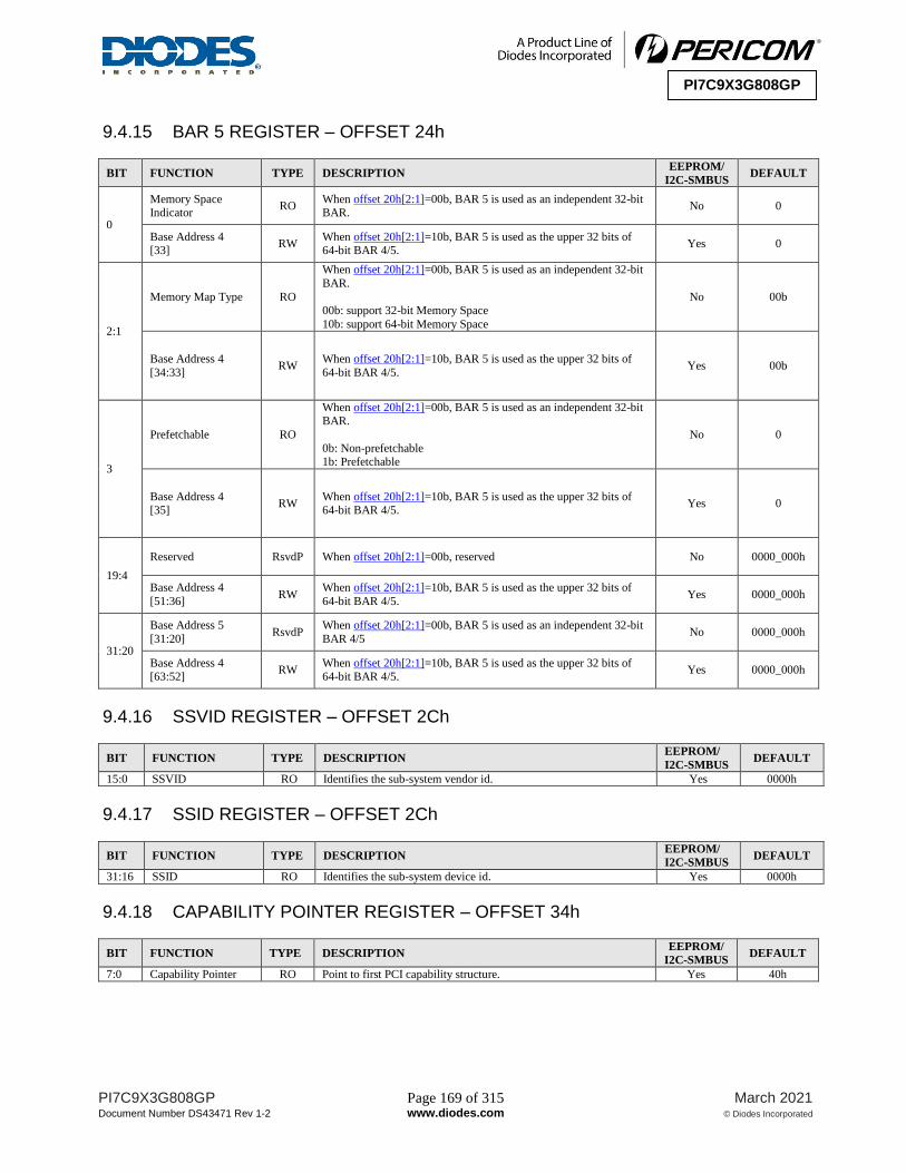
PI7C9X3G808GP Page 169 of 315 March 2021
Document Number DS43471 Rev 1-2 www.diodes.com © Diodes Incorporated
PI7C9X3G808GP
9.4.15 BAR 5 REGISTER – OFFSET 24h
BIT FUNCTION TYPE DESCRIPTION EEPROM/
I2C-SMBUS DEFAULT
0
Memory Space Indicator
RO When offset 20h[2:1]=00b, BAR 5 is used as an independent 32-bit BAR.
No 0
Base Address 4 [33]
RW When offset 20h[2:1]=10b, BAR 5 is used as the upper 32 bits of 64-bit BAR 4/5.
Yes 0
2:1
Memory Map Type RO
When offset 20h[2:1]=00b, BAR 5 is used as an independent 32-bit
BAR.
00b: support 32-bit Memory Space
10b: support 64-bit Memory Space
No 00b
Base Address 4
[34:33] RW
When offset 20h[2:1]=10b, BAR 5 is used as the upper 32 bits of
64-bit BAR 4/5. Yes 00b
3
Prefetchable RO
When offset 20h[2:1]=00b, BAR 5 is used as an independent 32-bit BAR.
0b: Non-prefetchable 1b: Prefetchable
No 0
Base Address 4 [35]
RW When offset 20h[2:1]=10b, BAR 5 is used as the upper 32 bits of 64-bit BAR 4/5.
Yes 0
19:4
Reserved RsvdP When offset 20h[2:1]=00b, reserved No 0000_000h
Base Address 4
[51:36] RW
When offset 20h[2:1]=10b, BAR 5 is used as the upper 32 bits of
64-bit BAR 4/5. Yes 0000_000h
31:20
Base Address 5
[31:20] RsvdP
When offset 20h[2:1]=00b, BAR 5 is used as an independent 32-bit
BAR 4/5 No 0000_000h
Base Address 4 [63:52]
RW When offset 20h[2:1]=10b, BAR 5 is used as the upper 32 bits of 64-bit BAR 4/5.
Yes 0000_000h
9.4.16 SSVID REGISTER – OFFSET 2Ch
BIT FUNCTION TYPE DESCRIPTION EEPROM/
I2C-SMBUS DEFAULT
15:0 SSVID RO Identifies the sub-system vendor id. Yes 0000h
9.4.17 SSID REGISTER – OFFSET 2Ch
BIT FUNCTION TYPE DESCRIPTION EEPROM/
I2C-SMBUS DEFAULT
31:16 SSID RO Identifies the sub-system device id. Yes 0000h
9.4.18 CAPABILITY POINTER REGISTER – OFFSET 34h
BIT FUNCTION TYPE DESCRIPTION EEPROM/
I2C-SMBUS DEFAULT
7:0 Capability Pointer RO Point to first PCI capability structure. Yes 40h

PI7C9X3G808GP Page 170 of 315 March 2021
Document Number DS43471 Rev 1-2 www.diodes.com © Diodes Incorporated
PI7C9X3G808GP
9.4.19 INTERRUPT LINE REGISTER – OFFSET 3Ch
BIT FUNCTION TYPE DESCRIPTION EEPROM/
I2C-SMBUS DEFAULT
7:0 Interrupt Line RW The interrupt line register communicates interrupt line routing
information. Yes 00h
9.4.20 INTERRUPT PIN REGISTER – OFFSET 3Ch
BIT FUNCTION TYPE DESCRIPTION EEPROM/
I2C-SMBUS DEFAULT
15:8 Interrupt Pin RO The Switch implements INTA virtual wire interrupt signal. Yes/No 01h
9.4.21 POWER MANAGEMENT CAPABILITIES REGISTER – OFFSET 40h
BIT FUNCTION TYPE DESCRIPTION EEPROM/
I2C-SMBUS DEFAULT
7:0 Enhanced
Capabilities ID RO
Read as 01h to indicate that this is power management capability
register. Yes 01h
15:8 Next Item Pointer RO Point to next PCI capability structure. Yes 48h
18:16 Power Management Revision
RO Read as 011b to indicate the device is compliant to Revision 1.2 of PCI Power Management Interface Specifications.
No 011b
19 PME# Clock RO Does not apply to PCI Express. Must be hardwired to 0. No 0
20 Reserved RsvdP Not support. No 0
21 Device specific Initialization
RO Read as 0b to indicate Switch does not have device specific initialization requirements.
Yes 0
24:22 AUX Current RO Reset to 000b. Yes 000b
25 D1 Power State Support
RO Read as 0b to indicate Switch does Not support the D1 power management state.
Yes 0
26 D2 Power State
Support RO
Read as 0b to indicate Switch does Not support the D2 power
management state. Yes 0
31:27 PME# Support RO Read as 19h to indicate Switch supports the forwarding of PME#
message in D0, D3 and D4 states. Yes C8h
9.4.22 POWER MANAGEMENT DATA REGISTER – OFFSET 44h
BIT FUNCTION TYPE DESCRIPTION EEPROM/
I2C-SMBUS DEFAULT
1:0 Power State RW
Indicates the current power state of the Switch. Writing a value of D0 when the previous state was D3 cause a hot reset without
asserting DWNRST_L.
00b: D0 state
01b: D1 state 10b: D2 state
11b: D3 hot state
Yes 00b
2 Reserved RsvdP Not support. No 0
3 No_Soft_Reset RO When set, this bit indicates that device transitioning from D3hot to D0 does not perform an internal reset. When clear, an internal reset
is performed when power state transits from D3hot to D0.
Yes 1
7:4 Reserved RsvdP Not support. No 0h
8 PME# Enable RW When asserted, the Switch will generate the PME# message. Yes 0
12:9 Data Select RW
Select data registers.
RW if offset 4C4h[9]=1 and RO if offset 4C4h[9]=0.
Yes 0h
14:13 Data Scale RO Reset to 00b. No/Yes 00b
15 PME Status RW1C Read as 0b as the PME# message is not implemented. Yes 0

PI7C9X3G808GP Page 171 of 315 March 2021
Document Number DS43471 Rev 1-2 www.diodes.com © Diodes Incorporated
PI7C9X3G808GP
9.4.23 PPB SUPPORT EXTENSIONS REGISTER – OFFSET 44h
BIT FUNCTION TYPE DESCRIPTION EEPROM/
I2C-SMBUS DEFAULT
21:16 Reserved RsvdP Not support. No 00h
22 B2_B3 Support for
D3HOT RsvdP Not support. No 0
23 Bus Power / Clock Control Enable
RsvdP Not support. No 0
9.4.24 DATA REGISTER– OFFSET 44h
BIT FUNCTION TYPE DESCRIPTION EEPROM/
I2C-SMBUS DEFAULT
31:24 Data Register RO Data Register. Yes 00h
9.4.25 MSI CAPABILITIES REGISTER – OFFSET 48h
BIT FUNCTION TYPE DESCRIPTION EEPROM/
I2C-SMBUS DEFAULT
7:0 Enhanced Capabilities ID
RO Read as 05h to indicate that this is message signal interrupt capability register.
No 05h
15:8 Next Item Pointer RO Point to next PCI capability structure. Yes 68h
16 MSI Enable RW
0b: The function is prohibited from using MSI to request service
1b: The function is permitted to use MSI to request service and is prohibited from using its INTx # pin
Yes 0
19:17 Multiple Message
Capable RO Indicate the number of requested vectors. Yes 011b
22:20 Multiple Message
Enable RW
Software writes to this field to indicate the number of allocated
vectors (equal to or less than the number of requested vectors.) Yes 000b
23 64-bit address
capable RO
0b: The function is not capable of generating a 64-bit message address
1b: The function is capable of generating a 64-bit message address
Yes 1b
24 Pre-vector Masking Capable
RO 1b: the function supports MSI pre-vector masking. 0b: the function does Not support MSI pre-vector masking.
Yes 1b
31:25 Reserved RO Not support. No 00h
9.4.26 MESSAGE ADDRESS REGISTER – OFFSET 4Ch
BIT FUNCTION TYPE DESCRIPTION EEPROM/
I2C-SMBUS DEFAULT
1:0 Reserved RsvdP Not support. No 00b
31:2 Message Address RW If the message enable bit is set, the contents of this register specify the DWORD aligned address for MSI memory write transaction.
Yes 0-0h
9.4.27 MESSAGE UPPER ADDRESS REGISTER – OFFSET 50h
BIT FUNCTION TYPE DESCRIPTION EEPROM/
I2C-SMBUS DEFAULT
31:0 Message Upper
Address RW
This register is only effective if the device supports a 64-bit
message address is set. Yes 0000_0000h
9.4.28 MESSAGE DATA REGISTER – OFFSET 54h
BIT FUNCTION TYPE DESCRIPTION EEPROM/
I2C-SMBUS DEFAULT
15:0 Message Data RW Message data. Yes 0000h

PI7C9X3G808GP Page 172 of 315 March 2021
Document Number DS43471 Rev 1-2 www.diodes.com © Diodes Incorporated
PI7C9X3G808GP
9.4.29 MESSAGE MASK REGISTER – OFFSET 58h
BIT FUNCTION TYPE DESCRIPTION EEPROM/
I2C-SMBUS DEFAULT
0 MSI Mask for Hot
Plug RW MSI mask for Hot Plug interrupts. Yes 0
1 MSI Mask for DPC RW MSI mask for DPC interrupts. Yes 0
2 MSI Mask for DMA
and GPIO RW MSI mask for DMAGPIO interrupts. Yes 0
3 MSI Mask for CDEP RW MSI mask for CDEP interrupts. Yes 0
4 Reserved RsvdP Not support. No 0
5 MSI Mask for
thermal sensor RW MSI mask for thermal sensor interrupts. Yes 0
7:6 Reserved RW Not support. No 00
31:8 Reserved RsvdP Not support. No 0000_000h
9.4.30 MESSAGE PENDING REGISTER – OFFSET 5Ch
BIT FUNCTION TYPE DESCRIPTION EEPROM/
I2C-SMBUS DEFAULT
0 MSI Pending for Hot
Plug Interrupts RO MSI pending status for Hot Plug interrupts. No 0
1 MSI Pending for DPC Interrupts
RO MSI pending status for DPC interrupts. No 0
2 MSI Pending for
GPIO Interrupts RO MSI pending status for GPIO interrupts. No 0
3 MSI Pending for
CDEP Interrupts RO MSI pending status for CDEP interrupts. No 0
4 Reserved RsvdP Not support. No 0
5 MSI Pending for thermal sensor
Interrupts
RO MSI pending status for thermal sensor interrupts. No 0
31:6 Reserved RsvdP Not support. No 0000_000h
9.4.31 PCI EXPRESS CAPABILITIES REGISTER – OFFSET 68h
BIT FUNCTION TYPE DESCRIPTION EEPROM/
I2C-SMBUS DEFAULT
7:0 Enhanced
Capabilities ID RO
Read as 10h to indicate that this is PCI express enhanced capability
register. No 10h
15:8 Next Item Pointer RO Point to next PCI capability structure. Yes A4h
19:16 Capability Version RO Read as 2h to indicate the device is compliant to Revision .2.0 of
PCI Express Base Specifications. Yes 2h
23:20 Device/Port Type RO Indicates the type of PCI Express logical device. Yes 00h
24 Slot Implemented RsvdP Not support. No 0
29:25 Interrupt Message
Number RO No MSI messages are generated in the transparent mode. No 00_000b
31:30 Reserved RsvdP Not support. No 00b
9.4.32 DEVICE CAPABILITIES REGISTER – OFFSET 6Ch
BIT FUNCTION TYPE DESCRIPTION EEPROM/
I2C-SMBUS DEFAULT
2:0 Max_Payload_Size
Supported RO
Indicates the maximum payload size that the device can support for
TLPs. Each port of the Switch supports 512 bytes max payload size. Yes/No 010b
4:3 Phantom Functions
Supported RO
Indicates the support for use of unclaimed function numbers as Phantom functions. Read as 00b, since the Switch does not act as a
requester.
No 00b
5 Extended Tag Field Supported
RO Indicates the maximum supported size of Tag field as a Requester. Read as 0, since the Switch does not act as a requester.
No 0
8:6 Endpoint L0s Acceptable Latency
RO
Acceptable total latency that an Endpoint can withstand due to the
transition from L0s state to the L0 state. For Switch, the ASPM software would not check this value.
No 111b

PI7C9X3G808GP Page 173 of 315 March 2021
Document Number DS43471 Rev 1-2 www.diodes.com © Diodes Incorporated
PI7C9X3G808GP
BIT FUNCTION TYPE DESCRIPTION EEPROM/
I2C-SMBUS DEFAULT
11:9 Endpoint L1 Acceptable Latency
RO Acceptable total latency that an Endpoint can withstand due to the transition from L1 state to the L0 state. For Switch, the ASPM
software would not check this value.
No 111b
14:12 Reserved RsvdP Not support. No 000b
15 Role_Based Error
Reporting RO
When set, indicates that the device implements the functionality
originally defined in the Error Reporting ECN. Yes 1
17:16 Reserved RsvdP Not support. No 00b
25:18 Captured Slot Power
Limit Value RO
In combination with the Slot Power Limit Scale value, specifies the
upper limit on power supplied by slot.
This value is set by the Set_Slot_Power_Limit message or
hardwired to 00h.
No 00h
27:26 Captured Slot Power
Limit Scale RO
Specifies the scale used for the Slot Power Limit Value.
This value is set by the Set_Slot_Power_Limit message or hardwired to 00b.
No 00b
31:28 Reserved RsvdP Not support. No 0h
9.4.33 DEVICE CONTROL REGISTER – OFFSET 70h
BIT FUNCTION TYPE DESCRIPTION EEPROM/
I2C-SMBUS DEFAULT
0 Correctable Error
Reporting Enable RW
0b: Disable Correctable Error Reporting
1b: Enable Correctable Error Reporting Yes 0
1 Non-Fatal Error
Reporting Enable RW
0b: Disable Non-Fatal Error Reporting
1b: Enable Non-Fatal Error Reporting Yes 0
2 Fatal Error Reporting
Enable RW
0b: Disable Fatal Error Reporting
1b: Enable Fatal Error Reporting Yes 0
3 Unsupported Request
Reporting Enable RW
0b: Disable Unsupported Request Reporting
1b: Enable Unsupported Request Reporting Yes 0
4 Enable Relaxed
Ordering RsvdP
When set, it permits the device to set the Relaxed Ordering bit in
the attribute field of transaction. Since the Switch can not either act
as a requester or alter the content of packet it forwards, this bit always returns ‘0’ when read.
No 0
7:5 Max_Payload_Size RW
This field sets maximum TLP payload size for the device.
Permissible values that can be programmed are indicated by the Max_Payload_Size Supported in the Device Capabilities register.
Any value exceeding the Max_Payload_Size Supported written to this register results into clamping to the Max_Payload_Size
Supported value.
Yes 000b
8 Extended Tag Field Enable
RW 0b: Disable Extended Tag Field 1b: Enable Extended Tag Field
Yes 0
9 Phantom Function
Enable RsvdP Does not apply to PCI Express Switch. Returns ‘0’ when read. No 0
10 Auxiliary (AUX) Power PM Enable
RO When set, indicates that a device is enabled to draw AUX power independent of PME AUX power.
No 0
11 Enable No Snoop RsvdP
When set, it permits to set the No Snoop bit in the attribute field of transaction. Since the Switch can not either act as a requester or
alter the content of packet it forwards, this bit always returns ‘0’
when read.
No 0
14:12 Max_Read_ Request_Size
RsvdP
This field sets the maximum Read Request size for the device as a
Requester. Since the Switch does not generate read request by itself,
these bits are hardwired to 000b.
No 000b
15 Reserved RsvdP Not support. No 0
9.4.34 DEVICE STATUS REGISTER – OFFSET 70h
BIT FUNCTION TYPE DESCRIPTION EEPROM/
I2C-SMBUS DEFAULT
16 Correctable Error Detected
RW1C
Asserted when correctable error is detected. Errors are logged in
this register regardless of whether error reporting is enabled or not in the Device Control register.
Yes 0

PI7C9X3G808GP Page 174 of 315 March 2021
Document Number DS43471 Rev 1-2 www.diodes.com © Diodes Incorporated
PI7C9X3G808GP
BIT FUNCTION TYPE DESCRIPTION EEPROM/
I2C-SMBUS DEFAULT
17 Non-Fatal Error Detected
RW1C Asserted when non-fatal error is detected. Errors are logged in this register regardless of whether error reporting is enabled or not in the
Device Control register.
Yes 0
18 Fatal Error Detected RW1C Asserted when fatal error is detected. Errors are logged in this register regardless of whether error reporting is enabled or not in the
Device Control register.
Yes 0
19 Unsupported Request Detected
RW1C
Asserted when unsupported request is detected. Errors are logged in
this register regardless of whether error reporting is enabled or not
in the Device Control register.
Yes 0
20 AUX Power
Detected RO Asserted when the AUX power is detected by the Switch No 0
21 Transactions Pending RO Each port of Switch does not issue Non-posted Requests on its own
behalf, so this bit is hardwired to 0b. No 0
31:22 Reserved RsvdP Not support. No 0-0h
9.4.35 LINK CAPABILITIES REGISTER – OFFSET 74h
BIT FUNCTION TYPE DESCRIPTION EEPROM/
I2C-SMBUS DEFAULT
3:0 Maximum Link
Speed RO
Indicates the maximum speed of the Express link is 8Gb/s, 5Gb/s
and 2.5 Gb/s.
0001b: 2.5 Gb/s 0001b: 5.0 Gb/s
0011b: 8.0 Gb/s
Others: Reserved
Yes 3h
9:4 Maximum Link Width
RO
Indicates the maximum width of the given PCIe Link. Valid widths
are x1, x2 or x4 which are set by PORTCFG[2:0] strap pins. Please
refer to Table 5-1 Mode Selection
00_0001b: x1 lane width 00_0010b: x2 lane width
00_0100b: x4 lane width
Yes Set by
PORTCFG
[2:0]
11:10 Active State Power Management
(ASPM) Support
RO Indicates the level of ASPM supported on the given PCIe Link.
Each port of Switch supports L0s and L1 entry. Yes 10b
14:12 L0s Exit Latency RO Indicates the L0s exit latency for the given PCIe Link. The length of time this port requires to complete transition from L0s
to L0 is in the range of 256ns to less than 512ns.
Yes 011b
17:15 L1 Exit
Latency RO
Indicates the L1 exit latency for the given PCIe Link. The length of time this port requires to complete transition from L1
to L0 is less than 1us.
Yes 000b
18 Clock Power
Management RO
Indicates that component tolerates the removal of any reference
clock via CLKREQ#. Yes 1
19 Surprise Down
Capability Enable RsvdP Not support. No 0
20
Data Link Layer
Active Reporting
Capable
RO
This bit must be set to 1b if the component supports the optional
capability of reporting the DL_Active state of the Data Link Control
and Management State Machine.
Yes 0
21 Link BW Notify
Cap. RsvdP Not support No 0
22 ASPM Optionality
Compliance RO
Software is permitted to use the value of this bit to help determine whether to enable ASPM or whether to run ASPM compliance
tests.
Yes 1
23 Reserved RsvdP Not support. No 0
31:24 Port Number RO Indicates the PCIe Port Number for the given PCIe Link. Yes 90h

PI7C9X3G808GP Page 175 of 315 March 2021
Document Number DS43471 Rev 1-2 www.diodes.com © Diodes Incorporated
PI7C9X3G808GP
9.4.36 LINK CONTROL REGISTER – OFFSET 78h
BIT FUNCTION TYPE DESCRIPTION EEPROM/
I2C-SMBUS DEFAULT
1:0
Active State Power
Management
(ASPM) Control
RW
00b: ASPM is Disabled
01b: L0s Entry Enabled 10b: L1 Entry Enabled
11b: L0s and L1 Entry Enabled
Note that the receiver must be capable of entering L0s even when
the field is disabled
Yes 00b
2 Reserved RsvdP Not support. No 0
3 Read Completion
Boundary (RCB) RsvdP Not support. No 0
4 Link Disable RW It disables the link when this bit is set. Yes 0
5 Retrain Link RW It initiates Link Retraining when this bit is set.
This bit always returns 0b when read.
Yes 0
6 Common Clock
Configuration RW
0b: The components at both ends of a link are operating with synchronous reference clock
1b: The components at both ends of a link are operating with a distributed common reference clock
Yes 0
7 Extended Synch RW
When set, it transmits 4096 FTS ordered sets in the L0s state for
entering L0 state and transmits 1024 TS1 ordered sets in the L1 state for entering L0 state.
Yes 0
8 Enable Clock Power Management
RW
0b: clock power management is disabled and must hold CLKREQ#
low 1b: device is permitted to use CLKREQ# to power manage Link
clock
Yes 0
9 HW Autonomous Width Disable
RW Reset to 0b. Yes 0
10
Link Bandwidth
Management Interrupt Enable
RsvdP Not support. No 0
11
Link Autonomous
Bandwidth Interrupt Enable
RsvdP Not support No 0
15:12 Reserved RsvdP Not support. No 0h
9.4.37 LINK STATUS REGISTER – OFFSET 78h
BIT FUNCTION TYPE DESCRIPTION EEPROM/
I2C-SMBUS DEFAULT
19:16 Link Speed RO
Indicate the negotiated speed of the Express link.
0001b: 2.5 Gb/s
0010b: 5.0 Gb/s 0011b: 8.0 Gb/s
Others: Reserved
No 0h
25:20 Negotiated Link
Width RO
Indicates the negotiated width of the given PCIe link.
00_0001b: x1 lane width 00_0010b: x2 lane width
00_0100b: x4 lane width
No
Set by
PORTCFG [2:0]
26 Training Error RO When set, indicates a Link training error occurred. This bit is cleared by hardware upon successful training of the link
to the L0 link state.
No 0
27 Link Training RO When set, indicates the link training is in progress. Hardware clears this bit once link training is complete.
No 0
28 Slot Clock Configuration
RO
0b: the Switch uses an independent clock irrespective of the
presence of a reference on the connector 1b: the Switch uses the same reference clock that the platform
provides on the connector
No 1

PI7C9X3G808GP Page 176 of 315 March 2021
Document Number DS43471 Rev 1-2 www.diodes.com © Diodes Incorporated
PI7C9X3G808GP
BIT FUNCTION TYPE DESCRIPTION EEPROM/
I2C-SMBUS DEFAULT
29 Data Link Layer
Link Active RO
Indicates the status of the Data Link Control and Management State Machine.
1b: indicate the DL_Active state
0b: otherwise
No 0
30 Link Bandwidth Management Status
RsvdP Not support. No 0
31 Link Autonomous
Bandwidth Status RsvdP Not support. No 0
9.4.38 SLOT CAPABILITIES REGISTER – OFFSET 7Ch
BIT FUNCTION TYPE DESCRIPTION EEPROM/
I2C-SMBUS DEFAULT
31:0 Reserved RsvdP Not support. No 0000_0000h
9.4.39 SLOT CONTROL REGISTER – OFFSET 80h
BIT FUNCTION TYPE DESCRIPTION EEPROM/
I2C-SMBUS DEFAULT
15:0 Reserved RsvdP Not support. No 0000h
9.4.40 SLOT STATUS REGISTER – OFFSET 80h
BIT FUNCTION TYPE DESCRIPTION EEPROM/
I2C-SMBUS DEFAULT
31:16 Reserved RsvdP Not support. No 0000h
9.4.41 DEVICE CAPABILITIES REGISTER 2 – OFFSET 8Ch
BIT FUNCTION TYPE DESCRIPTION EEPROM/
I2C-SMBUS DEFAULT
4:0 Reserved RsvdP Not support. No 0_0000b
5 ARI Forwarding Supported
RO 0b: ARI forwarding is Not supported 1b: ARI forwarding is supported
Yes/No 0
6 Reserved RsvdP Not support. No 0
10:7 Reserved RsvdP Not support. No 0-0b
11 Reserved RsvdP Not support. No 0
17:12 Reserved RsvdP Not support. No 0-0b
19:18 Reserved RsvdP Not support. No 00b
31:20 Reserved RsvdP Not support. No 000h
9.4.42 DEVICE CONTROL REGISTER 2 – OFFSET 90h
BIT FUNCTION TYPE DESCRIPTION EEPROM/
I2C-SMBUS DEFAULT
4:0 Reserved RsvdP Not support. No 0_0000b
5 ARI Forwarding
Enable RW
0b: disable
1b: enable Yes/No 0
6 Reserved RsvdP Not support. No 0
7 Reserved RsvdP Not support. No 0
9:8 Reserved RsvdP Not support. No 00b
10 Reserved RsvdP Not support. No 0
12:11 Reserved RsvdP Not support. No 00b
14:13 Reserved RsvdP Not support. No 00b
15 Reserved RsvdP Not support. No 0

PI7C9X3G808GP Page 177 of 315 March 2021
Document Number DS43471 Rev 1-2 www.diodes.com © Diodes Incorporated
PI7C9X3G808GP
9.4.43 DEVICE STATUS REGISTER 2 – OFFSET 90h
BIT FUNCTION TYPE DESCRIPTION EEPROM/
I2C-SMBUS DEFAULT
31:16 Reserved RsvdP Not support. No 0000h
9.4.44 LINK CAPABILITIES REGISTER 2 – OFFSET 94h
BIT FUNCTION TYPE DESCRIPTION EEPROM/
I2C-SMBUS DEFAULT
0 Reserved RsvdP Not support. No 0
7:1 Supported Link
Speeds Vector RO
This field indicates the supported Link speed of the associated Port.
bit[0]… 2.5 GT/s
bit[1]… 5.0 GT/s bit[2]… 8.0 GT/s
bit[6:3]… RsvdP
Yes 0000_111b
8 Crosslink Supported RO 0b: Crosslink is Not supported 1b: Crosslink is supported
Yes 0
31:9 Reserved RsvdP Not support. No 0-0b
9.4.45 LINK CONTROL REGISTER 2 – OFFSET 98h
BIT FUNCTION TYPE DESCRIPTION EEPROM/
I2C-SMBUS DEFAULT
3:0 Target Link Speed RW
0001b: 2.5GT/s link speed is supported 0010b: 5.0GT/s link speed is supported
0011b: 8.0GT/s link speed is supported
Others: reserved.
Yes 3h
4 Enter Compliance RW 1b: enter compliance Yes 0
5 HW_AutoSpeed_Dis RW
When set, this bit disables hardware from changing the link speed
for device-specific reasons other than attempting to correct unreliable link operation by reducing link speed.
Yes 0
6 Select_Deemp RO
Valid for downstream ports only.
0b: Select -3.5db de-emphasis
1b: Select -6.0 db de-emphasis
Yes/No 0
9:7 Tran_Margin RW This field controls the value of the non-deemphasized voltage level at the transmitter pins.
Yes 000b
10 Enter Modify Compliance
RW
Valid for upstream port only.
When set, the device transmits modified compliance pattern if the
LTSSM enters Polling.Compliance substate.
Yes 0
11 Compliance SOS RW
Valid for upstream port only.
When set, the LTSSM is required to send SKP Ordered Sets between sequences when sending the Compliance Pattern or
Modified Compliance Pattern.
Yes 0
15:12 Compliance Preset/De-emphasis
RW This field is intended for debug and compliance testing purpose. Yes 000b
9.4.46 LINK STATUS REGISTER 2 – OFFSET 98h
BIT FUNCTION TYPE DESCRIPTION EEPROM/
I2C-SMBUS DEFAULT
16 Current De-emphasis
level RO
1b: -3.5dB
0b: -6 dB No 1
17 Equalization
Complete RO
When set to 1b, this bit indicates that the Transmitter Equalization
procedure has completed. No 0
18 Equalization Phase 1
Successful RO
When set to 1b, this bit indicates that Phase 1 of Transmitter
Equalization procedure has successfully completed. No 0
19 Equalization Phase 2
Successful RO
When set to 1b, this bit indicates that Phase 2 of Transmitter
Equalization procedure has successfully completed. No 0

PI7C9X3G808GP Page 178 of 315 March 2021
Document Number DS43471 Rev 1-2 www.diodes.com © Diodes Incorporated
PI7C9X3G808GP
BIT FUNCTION TYPE DESCRIPTION EEPROM/
I2C-SMBUS DEFAULT
20 Equalization Phase 3 Successful
RO When set to 1b, this bit indicates that Phase 3 of Transmitter Equalization procedure has successfully completed.
No 0
21 Link Equalization
Request RW1C
This bit is set by hardware to request the Link equalization process
to be performed on the link. Yes/No 0
27:22 Reserved RsvdP Not support. No 0-0b
30:28 Downstream Component Presence
RO
This field indicates the presence and DRS status for the
Downstream Component.
000b: Link Down – Presence Not Determined 001b: Link Down – Component Not Present
010b: Link Down – Component Present
011b: Reserved
100b: Link Up – Component Present
101b: Link Up – Component Present and DRS Received 110b: Reserved
111b: Reserved
No 000b
31 DRS Message Received
RW1C This bit must be set whenever the Port receives a DRS message. Yes/No 0
9.4.47 SLOT CAPABILITIES REGISTER 2 – OFFSET 9Ch
BIT FUNCTION TYPE DESCRIPTION EEPROM/
I2C-SMBUS DEFAULT
31:0 Reserved RsvdP Not support. No 0000_0000h
9.4.48 SLOT CONTROL REGISTER 2 – OFFSET A0h
BIT FUNCTION TYPE DESCRIPTION EEPROM/
I2C-SMBUS DEFAULT
15:0 Reserved RsvdP Not support. No 0000_0000h
9.4.49 SLOT STATUS REGISTER 2 – OFFSET A0h
BIT FUNCTION TYPE DESCRIPTION EEPROM/
I2C-SMBUS DEFAULT
31:16 Reserved RsvdP Not support. No 0000_0000h
9.4.50 SSID/SSVID CAPATILITIES REGISTER – OFFSET A4h
BIT FUNCTION TYPE DESCRIPTION EEPROM/
I2C-SMBUS DEFAULT
7:0 SSID/SSVID Capabilities ID
RO Read as 0Dh to indicate that this is SSID/SSVID capability register. Yes 0Dh
15:8 Next Item Pointer RO Point to next PCI capability structure. Yes B0h
31:16 Reserved RsvdP Not support. No 0000h
9.4.51 SUBSYSTEM VENDOR ID REGISTER – OFFSET A8h
BIT FUNCTION TYPE DESCRIPTION EEPROM/
I2C-SMBUS DEFAULT
15:0 SSVID RO It indicates the sub-system vendor id. Yes 12D8h
9.4.52 SUBSYSTEM ID REGISTER – OFFSET A8h
BIT FUNCTION TYPE DESCRIPTION EEPROM/
I2C-SMBUS DEFAULT
31:16 SSID RO It indicates the sub-system device id. Yes C008h
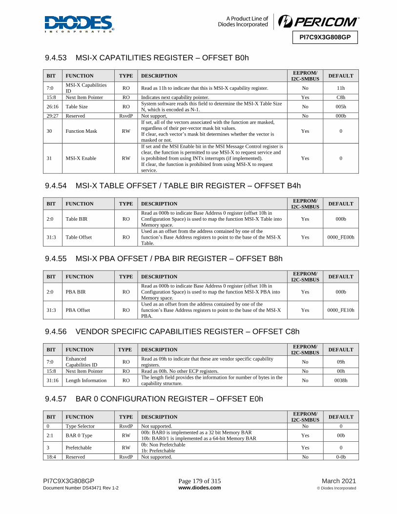
PI7C9X3G808GP Page 179 of 315 March 2021
Document Number DS43471 Rev 1-2 www.diodes.com © Diodes Incorporated
PI7C9X3G808GP
9.4.53 MSI-X CAPATILITIES REGISTER – OFFSET B0h
BIT FUNCTION TYPE DESCRIPTION EEPROM/
I2C-SMBUS DEFAULT
7:0 MSI-X Capabilities
ID RO Read as 11h to indicate that this is MSI-X capability register. No 11h
15:8 Next Item Pointer RO Indicates next capability pointer. Yes C8h
26:16 Table Size RO System software reads this field to determine the MSI-X Table Size
N, which is encoded as N-1. No 005h
29:27 Reserved RsvdP Not support, No 000b
30 Function Mask RW
If set, all of the vectors associated with the function are masked, regardless of their per-vector mask bit values.
If clear, each vector’s mask bit determines whether the vector is
masked or not.
Yes 0
31 MSI-X Enable RW
If set and the MSI Enable bit in the MSI Message Control register is
clear, the function is permitted to use MSI-X to request service and is prohibited from using INTx interrupts (if implemented).
If clear, the function is prohibited from using MSI-X to request
service.
Yes 0
9.4.54 MSI-X TABLE OFFSET / TABLE BIR REGISTER – OFFSET B4h
BIT FUNCTION TYPE DESCRIPTION EEPROM/
I2C-SMBUS DEFAULT
2:0 Table BIR RO
Read as 000b to indicate Base Address 0 register (offset 10h in
Configuration Space) is used to map the function MSI-X Table into
Memory space.
Yes 000b
31:3 Table Offset RO
Used as an offset from the address contained by one of the
function’s Base Address registers to point to the base of the MSI-X
Table.
Yes 0000_FE00h
9.4.55 MSI-X PBA OFFSET / PBA BIR REGISTER – OFFSET B8h
BIT FUNCTION TYPE DESCRIPTION EEPROM/
I2C-SMBUS DEFAULT
2:0 PBA BIR RO
Read as 000b to indicate Base Address 0 register (offset 10h in
Configuration Space) is used to map the function MSI-X PBA into
Memory space.
Yes 000b
31:3 PBA Offset RO
Used as an offset from the address contained by one of the
function’s Base Address registers to point to the base of the MSI-X PBA.
Yes 0000_FE10h
9.4.56 VENDOR SPECIFIC CAPABILITIES REGISTER – OFFSET C8h
BIT FUNCTION TYPE DESCRIPTION EEPROM/
I2C-SMBUS DEFAULT
7:0 Enhanced
Capabilities ID RO
Read as 09h to indicate that these are vendor specific capability
registers. No 09h
15:8 Next Item Pointer RO Read as 00h. No other ECP registers. No 00h
31:16 Length Information RO The length field provides the information for number of bytes in the
capability structure. No 0038h
9.4.57 BAR 0 CONFIGURATION REGISTER – OFFSET E0h
BIT FUNCTION TYPE DESCRIPTION EEPROM/
I2C-SMBUS DEFAULT
0 Type Selector RsvdP Not supported. No 0
2:1 BAR 0 Type RW 00b: BAR0 is implemented as a 32 bit Memory BAR 10b: BAR0/1 is implemented as a 64-bit Memory BAR
Yes 00b
3 Prefetchable RW 0b: Non Prefetchable
1b: Prefetchable Yes 0
18:4 Reserved RsvdP Not supported. No 0-0b

PI7C9X3G808GP Page 180 of 315 March 2021
Document Number DS43471 Rev 1-2 www.diodes.com © Diodes Incorporated
PI7C9X3G808GP
BIT FUNCTION TYPE DESCRIPTION EEPROM/
I2C-SMBUS DEFAULT
30:19 BAR 0 Size RW
To specify BAR0 size.
0b: Corresponding BAR0 bits are RO bits that always return 0 1b: Corresponding BAR0 bits are RW bits
Yes FFFh
31
BAR 0 Enable RW bit[2:1]=00b 0b: Disable BAR0
1b: Enable BAR0 Yes 1
BAR 0 Size RW bit[2:1]=10b Includes with bit[30:19] when this BAR is used as
a 64-bit BAR (bit[2:1]=10b).
9.4.58 BAR 0-1 CONFIGURATION REGISTER – OFFSET E4h
BIT FUNCTION TYPE DESCRIPTION EEPROM/
I2C-SMBUS DEFAULT
0 Type Selector
RsvdP E0h[2:1]=00b Not support. No 0
RW E0h[2:1]=10b BAR0/1 are used as a 64-bit BAR, bit[31:0] are
used as the upper 32-bits. Yes 0
2:1 BAR 1 Type
RO E0h[2:1]=00b 00b: BAR1 is implemented as 32 bit Memory
BAR. Yes 00b
RW E0h[2:1]=10b BAR0/1 are used as a 64-bit BAR, bit[31:0] are
used as the upper 32-bits. Yes 00b
3 Prefetchable
RW E0h[2:1]=00b 0b: Non Prefetchable 1b: Prefetchable
Yes 0
RW E0h[2:1]=10b BAR0/1 are used as a 64-bit BAR, bit[31:0] are
used as the upper 32-bits.
4 Reserved
RsvdP E0h[2:1]=00b Not support. No 0
RW E0h[2:1]=10b BAR0/1 are used as a 64-bit BAR, bit[31:0] are
used as the upper 32-bits. Yes 0
8:5 Switch ID
RW E0h[2:1]=00b The valid number is from 0 to 5.
Yes 0000b
RW E0h[2:1]=10b BAR0/1 are used as a 64-bit BAR, bit[31:0] are
used as the upper 32-bits.
19:9 Reserved
RsvdP E0h[2:1]=00b Not support. No 0-0b
RW E0h[2:1]=10b BAR0/1 are used as a 64-bit BAR, bit[31:0] are
used as the upper 32-bits. Yes 0-0b
30:20 BAR 1 Size RW
To specify BAR1 size.
0b: Corresponding BAR1 bits are RO bits that always return 0 1b: Corresponding BAR1 bits are RW bits
Yes 000h
31
BAR 1 Enable RW E0h[2:1]=00b 0b: Disable BAR1
1b: Enable BAR1 Yes 0
64-Bit BAR RW E0h[2:1]=10b 0b: BAR0/1 is disabled; all BAR0/1 bits read 0.
1b: BAR0/1 is enabled as a 64-bit BAR.
9.4.59 BAR 2 CONFIGURATION REGISTER – OFFSET E8h
BIT FUNCTION TYPE DESCRIPTION EEPROM/
I2C-SMBUS DEFAULT
0 Type Selector RsvdP Not supported. No 0
2:1 BAR2 Type RW 00b: BAR2 is implemented as a 32 bit Memory BAR 10b: BAR2/3 is implemented as a 64-bit Memory BAR
Yes 00b
3 Prefetchable RW 0b: Non Prefetchable
1b: Prefetchable Yes 0
4 LUT/DAT Selection RW 0b: BAR2/3 is used for Address Look-up Translation.
1b: BAR2/3 is used for Direct Address Translation. Yes 0
8:5 Domain ID RW The valid number is from 0 to 11. Yes 0000b
19:9 Reserved RsvdP Not supported. No 0-0b

PI7C9X3G808GP Page 181 of 315 March 2021
Document Number DS43471 Rev 1-2 www.diodes.com © Diodes Incorporated
PI7C9X3G808GP
BIT FUNCTION TYPE DESCRIPTION EEPROM/
I2C-SMBUS DEFAULT
30:20 BAR2 Size RW
To specify BAR2 size.
0b: Corresponding BAR2 bits are RO bits that always return 0 1b: Corresponding BAR2 bits are RW bits
It implies the minimum window size is 1MB and minimum page size is 8KB, which is windows size divided by 128 (number of LUT
entries).
Yes 7FFh
31
BAR 2 Enable RW bit[2:1]=00b 0b: Disable BAR2 1b: Enable BAR2
Yes 1
BAR 2 Size RW bit[2:1]=10b Includes with bit[30:20] when this BAR is used as a 64-bit BAR (bit[2:1]=10b).
9.4.60 BAR 2-3 CONFIGURATION REGISTER – OFFSET ECh
BIT FUNCTION TYPE DESCRIPTION EEPROM/
I2C-SMBUS DEFAULT
0 Type Selector
RsvdP E8h[2:1]=00b Not support. No 0
RW E8h[2:1]=10b BAR2/3 are used as a 64-bit BAR, bit[31:0] are used as the upper 32-bits.
Yes 0
2:1 BAR3 Type
RO E8h[2:1]=00b 00b: BAR3 is implemented as 32 bit Memory
BAR. No 00b
RW E8h[2:1]=10b BAR2/3 are used as a 64-bit BAR, bit[31:0] are used as the upper 32-bits.
Yes/No 00b
3 Prefetchable
RW E8h[2:1]=00b 0b: Non Prefetchable
1b: Prefetchable Yes 0
RW E8h[2:1]=10b BAR2/3 are used as a 64-bit BAR, bit[31:0] are used as the upper 32-bits.
4 Reserved
RsvdP E8h[2:1]=00b Not support. No 0
RW E8h[2:1]=10b BAR2/3 are used as a 64-bit BAR, bit[31:0] are used as the upper 32-bits.
Yes 0
8:5 Domain ID
RW E8h[2:1]=00b The valid number is from 0 to 11.
Yes 0000b
RW E8h[2:1]=10b BAR2/3 are used as a 64-bit BAR, bit[31:0] are used as the upper 32-bits.
19:9 Reserved
RsvdP E8h[2:1]=00b Not support. No 0-0b
RW E8h[2:1]=10b BAR2/3 are used as a 64-bit BAR, bit[31:0] are used as the upper 32-bits.
Yes 0-0b
30:20 BAR3 Size RW
To specify BAR3 size.
0b: Corresponding BAR3 bits are RO bits that always return 0
1b: Corresponding BAR3 bits are RW bits
Yes 000h
31
BAR 3 Enable RW E8h[2:1]=00b 0b: Disable BAR3 1b: Enable BAR3
Yes 0
64-Bit BAR RW E8h[2:1]=10b 0b: BAR2/3 is disabled; all BAR2/3 bits read 0.
1b: BAR2/3 is enabled as a 64-bit BAR.
9.4.61 BAR 4 CONFIGURATION REGISTER – OFFSET F0h
BIT FUNCTION TYPE DESCRIPTION EEPROM/
I2C-SMBUS DEFAULT
0 Type Selector RsvdP Not supported. No 0
2:1 BAR4 Type RW 00b: BAR4 is implemented as a 32 bit Memory BAR
10b: BAR4/5 is implemented as a 64-bit Memory BAR Yes 00b
3 Prefetchable RW 0b: Non Prefetchable
1b: Prefetchable Yes 0
4 Reserved RsvdP Not support. No 0
8:5 Partition ID RW The valid number is from 0 to 11. Yes 0000b
19:9 Reserved RsvdP Not supported. No 0-0b

PI7C9X3G808GP Page 182 of 315 March 2021
Document Number DS43471 Rev 1-2 www.diodes.com © Diodes Incorporated
PI7C9X3G808GP
BIT FUNCTION TYPE DESCRIPTION EEPROM/
I2C-SMBUS DEFAULT
30:20 BAR 4 Size RW
To specify BAR4 size.
0b: Corresponding BAR4 bits are RO bits that always return 0 1b: Corresponding BAR4 bits are RW bits
It implies the minimum window size is 1MB and minimum page size is 8KB, which is windows size divided by 128 (number of LUT
entries).
Yes 7FFh
31
BAR 4 Enable RW bit[2:1]=00b 0b: Disable BAR4 1b: Enable BAR4
Yes 1
BAR 4 Size RW bit[2:1]=10b Includes with bit[30:20] when this BAR is used as a 64-bit BAR (bit[2:1]=10b).
9.4.62 BAR 4-5 CONFIGURATION REGISTER – OFFSET F4h
BIT FUNCTION TYPE DESCRIPTION EEPROM/
I2C-SMBUS DEFAULT
0 Type Selector
RsvdP F0h[2:1]=00b Not support. No 0
RW F0h[2:1]=10b BAR4/5 are used as a 64-bit BAR, bit[31:0]are used as the upper 32-bits.
Yes 0
2:1 BAR 5 Type
RO F0h[2:1]=00b 00b: BAR5 is implemented as 32 bit Memory
BAR. Yes 00b
RW F0h[2:1]=10b BAR4/5 are used as a 64-bit BAR, bit[31:0]are used as the upper 32-bits.
Yes 00b
3 Prefetchable
RW F0h[2:1]=00b 0b: Non Prefetchable
1b: Prefetchable Yes 0
RW F0h[2:1]=10b BAR4/5 are used as a 64-bit BAR, bit[31:0]are used as the upper 32-bits.
4 Reserved
RsvdP F0h[2:1]=00b Not support. No 0
RW F0h[2:1]=10b BAR4/5 are used as a 64-bit BAR, bit[31:0] are used as the upper 32-bits.
Yes 0
8:5 Domain/Switch ID
RW F0h[2:1]=00b The valid domain number is from 0 to 3.
Yes 0000b
RW F0h[2:1]=10b BAR4/5 are used as a 64-bit BAR, bit[31:0] are used as the upper 32-bits.
19:9 Reserved
RsvdP F0h[2:1]=00b Not support. No 0-0b
RW F0h[2:1]=10b BAR4/5 are used as a 64-bit BAR, bit[31:0]are used as the upper 32-bits.
Yes 0-0b
30:20 BAR 5 Size RW
To specify BAR5 size.
0b: Corresponding BA5 bits are RO bits that always return 0
1b: Corresponding BAR5 bits are RW bits
Yes 000h
31
BAR 5 Enable RW F0h[2:1]=00b 0b: Disable BAR5 1b: Enable BAR5
Yes 0
64-Bit BAR RW F0h[2:1]=10b 0b: BAR4/5 is disabled; all BAR4/5 bits read 0.
1b: BAR4/5 is enabled as a 64-bit BAR.
9.4.63 PCI EXPRESS ADVANCED ERROR REPORTING ENHANCED CAPABILITY HEADER REGISTER – OFFSET 100h
BIT FUNCTION TYPE DESCRIPTION EEPROM/
I2C-SMBUS DEFAULT
15:0 Extended
Capabilities ID RO
Read as 0001h to indicate that this is PCI express extended
capability register for advance error reporting. No 0001h
19:16 Capability Version RO Read as 1h. No 1h
31:20 Next Capability
Offset RO Point to next PCI extended capability structure. Yes 130h
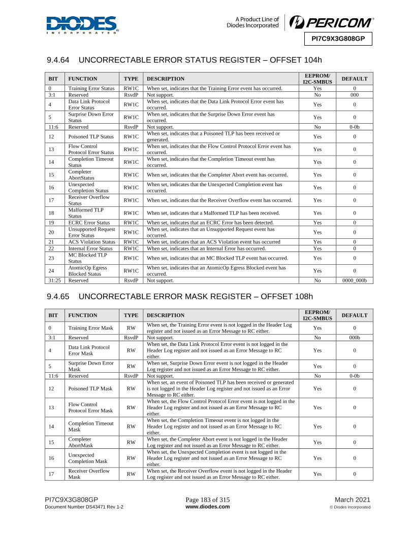
PI7C9X3G808GP Page 183 of 315 March 2021
Document Number DS43471 Rev 1-2 www.diodes.com © Diodes Incorporated
PI7C9X3G808GP
9.4.64 UNCORRECTABLE ERROR STATUS REGISTER – OFFSET 104h
BIT FUNCTION TYPE DESCRIPTION EEPROM/
I2C-SMBUS DEFAULT
0 Training Error Status RW1C When set, indicates that the Training Error event has occurred. Yes 0
3:1 Reserved RsvdP Not support. No 000
4 Data Link Protocol Error Status
RW1C When set, indicates that the Data Link Protocol Error event has occurred.
Yes 0
5 Surprise Down Error
Status RW1C
When set, indicates that the Surprise Down Error event has
occurred. Yes 0
11:6 Reserved RsvdP Not support. No 0-0b
12 Poisoned TLP Status RW1C When set, indicates that a Poisoned TLP has been received or
generated. Yes 0
13 Flow Control Protocol Error Status
RW1C When set, indicates that the Flow Control Protocol Error event has occurred.
Yes 0
14 Completion Timeout
Status RW1C
When set, indicates that the Completion Timeout event has
occurred. Yes 0
15 Completer
AbortStatus RW1C When set, indicates that the Completer Abort event has occurred. Yes 0
16 Unexpected Completion Status
RW1C When set, indicates that the Unexpected Completion event has occurred.
Yes 0
17 Receiver Overflow
Status RW1C When set, indicates that the Receiver Overflow event has occurred. Yes 0
18 Malformed TLP Status
RW1C When set, indicates that a Malformed TLP has been received. Yes 0
19 ECRC Error Status RW1C When set, indicates that an ECRC Error has been detected. Yes 0
20 Unsupported Request Error Status
RW1C When set, indicates that an Unsupported Request event has occurred.
Yes 0
21 ACS Violation Status RW1C When set, indicates that an ACS Violation event has occurred Yes 0
22 Internal Error Status RW1C When set, indicates that an Internal Error has occurred. Yes 0
23 MC Blocked TLP Status
RW1C When set, indicates that an MC Blocked TLP event has occurred. Yes 0
24 AtomicOp Egress
Blocked Status RW1C
When set, indicates that an AtomicOp Egress Blocked event has
occurred. Yes 0
31:25 Reserved RsvdP Not support. No 0000_000b
9.4.65 UNCORRECTABLE ERROR MASK REGISTER – OFFSET 108h
BIT FUNCTION TYPE DESCRIPTION EEPROM/
I2C-SMBUS DEFAULT
0 Training Error Mask RW When set, the Training Error event is not logged in the Header Log
register and not issued as an Error Message to RC either. Yes 0
3:1 Reserved RsvdP Not support. No 000b
4 Data Link Protocol Error Mask
RW
When set, the Data Link Protocol Error event is not logged in the
Header Log register and not issued as an Error Message to RC either.
Yes 0
5 Surprise Down Error
Mask RW
When set, Surprise Down Error event is not logged in the Header
Log register and not issued as an Error Message to RC either. Yes 0
11:6 Reserved RsvdP Not support. No 0-0b
12 Poisoned TLP Mask RW
When set, an event of Poisoned TLP has been received or generated
is not logged in the Header Log register and not issued as an Error
Message to RC either.
Yes 0
13 Flow Control Protocol Error Mask
RW
When set, the Flow Control Protocol Error event is not logged in the
Header Log register and not issued as an Error Message to RC
either.
Yes 0
14 Completion Timeout Mask
RW
When set, the Completion Timeout event is not logged in the
Header Log register and not issued as an Error Message to RC
either.
Yes 0
15 Completer
AbortMask RW
When set, the Completer Abort event is not logged in the Header
Log register and not issued as an Error Message to RC either. Yes 0
16 Unexpected
Completion Mask RW
When set, the Unexpected Completion event is not logged in the Header Log register and not issued as an Error Message to RC
either.
Yes 0
17 Receiver Overflow Mask
RW When set, the Receiver Overflow event is not logged in the Header Log register and not issued as an Error Message to RC either.
Yes 0

PI7C9X3G808GP Page 184 of 315 March 2021
Document Number DS43471 Rev 1-2 www.diodes.com © Diodes Incorporated
PI7C9X3G808GP
BIT FUNCTION TYPE DESCRIPTION EEPROM/
I2C-SMBUS DEFAULT
18 Malformed TLP Mask
RW When set, an event of Malformed TLP has been received is not logged in the Header Log register and not issued as an Error
Message to RC either.
Yes 0
19 ECRC Error Mask RW When set, an event of ECRC Error has been detected is not logged in the Header Log register and not issued as an Error Message to
RC either.
Yes 0
20 Unsupported Request Error Mask
RW
When set, the Unsupported Request event is not logged in the
Header Log register and not issued as an Error Message to RC
either.
Yes 0
21 ACS Violation Mask RW When set, the ACS Violation event is not logged in the Header Log
regiter and not issued as an Error Message toRC either. Yes 0
22 Internal Error Mask RW When set, the Internal Error event is not logged in the Header Log
register and not issued as an Error Message to RC either. Yes 1
23 MC Blocked TLP
Mask RW
When set, the MC Blocked TLP event is not logged in the Header
Log register and not issued as an Error Message to RC either. Yes 0
24 AtomicOp Egress Blocked Mask
RW When set, the AtomicOp Egress Blocked event is not logged in the Header Log register and not issued as an Error Message to RC
either.
Yes 0
31:25 Reserved RsvdP Not support. No 0000_000b
9.4.66 UNCORRECTABLE ERROR SEVERITY REGISTER – OFFSET 10Ch
BIT FUNCTION TYPE DESCRIPTION EEPROM/
I2C-SMBUS DEFAULT
0 Training Error
Severity RW
0b: Non-Fatal
1b: Fatal Yes 1
3:1 Reserved RsvdP Not support. No 000b
4 Data Link Protocol
Error Severity RW
0b: Non-Fatal
1b: Fatal Yes 1
5 Surprise Down Error Severity
RW 0b: Non-Fatal 1b: Fatal
Yes 1
11:6 Reserved RsvdP Not support. No 0-0b
12 Poisoned TLP
Severity RW
0b: Non-Fatal
1b: Fatal Yes 0
13
Flow Control
Protocol Error
Severity
RW 0b: Non-Fatal 1b: Fatal
Yes 1
14 Completion Timeout
Error Severity RW
0b: Non-Fatal
1b: Fatal Yes 0
15 Completer AbortSeverity
RW 0b: Non-Fatal 1b: Fatal
Yes 0
16 Unexpected
Completion Severity RW
0b: Non-Fatal
1b: Fatal Yes 0
17 Receiver Overflow
Severity RW
0b: Non-Fatal
1b: Fatal Yes 1
18 Malformed TLP Severity
RW 0b: Non-Fatal 1b: Fatal
Yes 1
19 ECRC Error Severity RW 0b: Non-Fatal
1b: Fatal Yes 0
20 Unsupported Request Error Severity
RW 0b: Non-Fatal 1b: Fatal
Yes 0
21 ACS Violation Severity
RW 0b: Non-Fatal 1b: Fatal
Yes 0
22 Internal Error
Severity RW
0b: Non-Fatal
1b: Fatal Yes 1
23 MC Blocked TLP Severity
RW 0b: Non-Fatal 1b: Fatal
Yes 0
24 AtomicOp Egress
Blocked Severity RW
0b: Non-Fatal
1b: Fatal Yes 0
31:25 Reserved RsvdP Not support. No 0000_000b
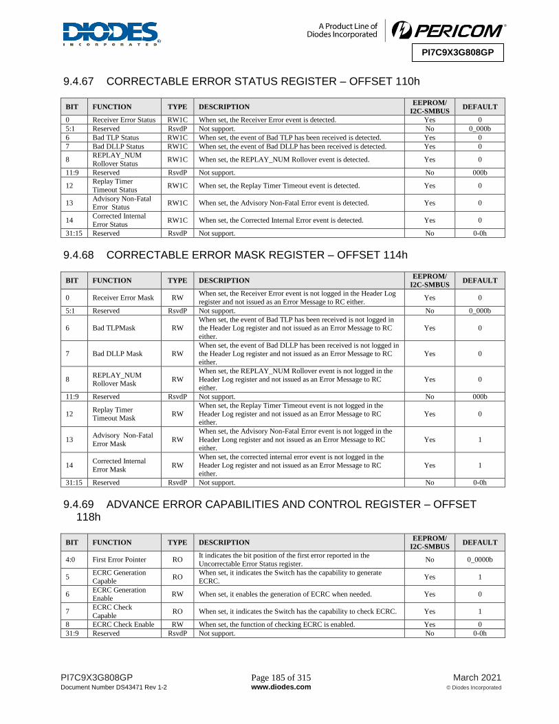
PI7C9X3G808GP Page 185 of 315 March 2021
Document Number DS43471 Rev 1-2 www.diodes.com © Diodes Incorporated
PI7C9X3G808GP
9.4.67 CORRECTABLE ERROR STATUS REGISTER – OFFSET 110h
BIT FUNCTION TYPE DESCRIPTION EEPROM/
I2C-SMBUS DEFAULT
0 Receiver Error Status RW1C When set, the Receiver Error event is detected. Yes 0
5:1 Reserved RsvdP Not support. No 0_000b
6 Bad TLP Status RW1C When set, the event of Bad TLP has been received is detected. Yes 0
7 Bad DLLP Status RW1C When set, the event of Bad DLLP has been received is detected. Yes 0
8 REPLAY_NUM
Rollover Status RW1C When set, the REPLAY_NUM Rollover event is detected. Yes 0
11:9 Reserved RsvdP Not support. No 000b
12 Replay Timer
Timeout Status RW1C When set, the Replay Timer Timeout event is detected. Yes 0
13 Advisory Non-Fatal Error Status
RW1C When set, the Advisory Non-Fatal Error event is detected. Yes 0
14 Corrected Internal
Error Status RW1C When set, the Corrected Internal Error event is detected. Yes 0
31:15 Reserved RsvdP Not support. No 0-0h
9.4.68 CORRECTABLE ERROR MASK REGISTER – OFFSET 114h
BIT FUNCTION TYPE DESCRIPTION EEPROM/
I2C-SMBUS DEFAULT
0 Receiver Error Mask RW When set, the Receiver Error event is not logged in the Header Log
register and not issued as an Error Message to RC either. Yes 0
5:1 Reserved RsvdP Not support. No 0_000b
6 Bad TLPMask RW When set, the event of Bad TLP has been received is not logged in the Header Log register and not issued as an Error Message to RC
either.
Yes 0
7 Bad DLLP Mask RW When set, the event of Bad DLLP has been received is not logged in the Header Log register and not issued as an Error Message to RC
either.
Yes 0
8 REPLAY_NUM Rollover Mask
RW
When set, the REPLAY_NUM Rollover event is not logged in the
Header Log register and not issued as an Error Message to RC
either.
Yes 0
11:9 Reserved RsvdP Not support. No 000b
12 Replay Timer Timeout Mask
RW
When set, the Replay Timer Timeout event is not logged in the
Header Log register and not issued as an Error Message to RC either.
Yes 0
13 Advisory Non-Fatal
Error Mask RW
When set, the Advisory Non-Fatal Error event is not logged in the
Header Long register and not issued as an Error Message to RC either.
Yes 1
14 Corrected Internal
Error Mask RW
When set, the corrected internal error event is not logged in the
Header Log register and not issued as an Error Message to RC
either.
Yes 1
31:15 Reserved RsvdP Not support. No 0-0h
9.4.69 ADVANCE ERROR CAPABILITIES AND CONTROL REGISTER – OFFSET 118h
BIT FUNCTION TYPE DESCRIPTION EEPROM/
I2C-SMBUS DEFAULT
4:0 First Error Pointer RO It indicates the bit position of the first error reported in the
Uncorrectable Error Status register. No 0_0000b
5 ECRC Generation
Capable RO
When set, it indicates the Switch has the capability to generate
ECRC. Yes 1
6 ECRC Generation Enable
RW When set, it enables the generation of ECRC when needed. Yes 0
7 ECRC Check
Capable RO When set, it indicates the Switch has the capability to check ECRC. Yes 1
8 ECRC Check Enable RW When set, the function of checking ECRC is enabled. Yes 0
31:9 Reserved RsvdP Not support. No 0-0h

PI7C9X3G808GP Page 186 of 315 March 2021
Document Number DS43471 Rev 1-2 www.diodes.com © Diodes Incorporated
PI7C9X3G808GP
9.4.70 HEADER LOG REGISTER – OFFSET From 11Ch to 128h
BIT FUNCTION TYPE DESCRIPTION EEPROM/
I2C-SMBUS DEFAULT
31:0 1st DWORD RO Hold the 1st DWORD of TLP Header. The Head byte is in big
endian. No 0000_0000h
63:32 2nd DWORD RO Hold the 2nd DWORD of TLP Header. The Head byte is in big endian.
No 0000_0000h
95:64 3rd DWORD RO Hold the 3rd DWORD of TLP Header. The Head byte is in big
endian. No 0000_0000h
127:96 4th DWORD RO Hold the 4th DWORD of TLP Header. The Head byte is in big
endian. No 0000_0000h
9.4.71 PCI EXPRESS VIRTUAL CHANNEL ENHANCED CAPABILITYHEADER REGISTER – OFFSET 130h
BIT FUNCTION TYPE DESCRIPTION EEPROM/
I2C-SMBUS DEFAULT
15:0 Extended Capabilities ID
RO Read as 0002h to indicate that this is PCI express extended capability register for virtual channel.
No 02h
19:16 Capability Version RO Read as 1h. No 1h
31:20 Next Capability
Offset RO Point to next PCI extended capability strcture. Yes 1A0h
9.4.72 PORT VC CAPABILITY REGISTER 1 – OFFSET 134h
BIT FUNCTION TYPE DESCRIPTION EEPROM/
I2C-SMBUS DEFAULT
2:0 Extended VC Count RO It indicates the number of extended Virtual Channels in addition to
the default VC supported by the Switch. No 000b
3 Reserved RO Not support. No 0
6:4 Low Priority
Extended VC Count RO
It indicates the number of extended Virtual Channels in addition to
the default VC belonging to the low-priority VC (LPVC) group. No 000b
7 Reserved RO Not support. No 0
9:8 Reference Clock RO It indicates the reference clock for Virtual Channels that support time-based WRR Port Arbitration. Defined encoding is 00b for 100
ns reference clock.
No 00b
11:10 Port Arbitration Table Entry Size
RO Read as 10b to indicate the size of Port Arbitration table entry in the device is 4 bits.
No 10b
31:12 Reserved RsvdP Not support. No 0000_0h
9.4.73 PORT VC CAPABILITY REGISTER 2 – OFFSET 138h
BIT FUNCTION TYPE DESCRIPTION EEPROM/
I2C-SMBUS DEFAULT
7:0 VC Arbitration Capability
RO
It indicates the types of VC Arbitration supported by the device for the LPVC group. This field is valid when LPVC is greater
than 0. The Switch supports Hardware fixed arbitration scheme,
e.g., Round Robin and Weight Round Robin arbitration with 32 phases in LPVC.
No 00h
23:8 Reserved RsvdP Not support. No 0000h
31:24 VC Arbitration Table
Offset RO
It indicates the location of the VC Arbitration Table as an offset from the base address of the Virtual Channel Capability register
in the unit of DQWD (16 bytes).
No 00h
9.4.74 PORT VC CONTROL REGISTER – OFFSET 13Ch
BIT FUNCTION TYPE DESCRIPTION EEPROM/
I2C-SMBUS DEFAULT
0 Load VC Arbitration Table
WO When set, the programmed VC Arbitration Table is applied to the hardware. This bit always returns 0b when read.
Yes/No 0

PI7C9X3G808GP Page 187 of 315 March 2021
Document Number DS43471 Rev 1-2 www.diodes.com © Diodes Incorporated
PI7C9X3G808GP
BIT FUNCTION TYPE DESCRIPTION EEPROM/
I2C-SMBUS DEFAULT
3:1 VC Arbitration
Select RW
This field is used to configure the VC Arbitration by selecting one of the supported VC Arbitration schemes. The valid values for the
schemes supported by Switch are 0b and 1b. Other value than these written into this register will be treated as default.
Yes/No 000b
15:4 Reserved RsvdP Not support. No 000h
9.4.75 PORT VC STATUS REGISTER – OFFSET 13Ch
BIT FUNCTION TYPE DESCRIPTION EEPROM/
I2C-SMBUS DEFAULT
16 VC Arbitration Table Status
RO
When set, it indicates that any entry of the VC Arbitration Table is
written by software. This bit is cleared when hardware finishes loading values stored in the VC Arbitration Table after the bit of
“Load VC Arbitration Table” is set.
No 0
31:17 Reserved RsvdP Not support. No 0-0h
9.4.76 VC RESOURCE CAPABILITY REGISTER (0) – OFFSET 140h
BIT FUNCTION TYPE DESCRIPTION EEPROM/
I2C-SMBUS DEFAULT
7:0 Port Arbitration Capability
RO
It indicates the types of Port Arbitration supported by the VC
resource. The Switch supports Round Robin Hardware fixed arbitration scheme.
No 01h
13:8 Reserved RsvdP Not support. No 00_0000h
14 Advanced Packet
Switching RO
When set, it indicates the VC resource only supports transaction
optimized for Advanced Packet Switching (AS). No 0
15 Reject Snoop
Transactions RsvdP Not support. No 0
22:16 Maximum Time Slots
RO It indicates the maximum numbers of time slots (minus one) are allocated for Isochronous traffic.
No 3Fh
23 Reserved RsvdP Not support. No 0
31:24 Port Arbitration
Table Offset RO
It indicates the location of the Port Arbitration Table (n) as an offset from the base address of the Virtual Channel Capability register in
the unit of DQWD (16 bytes).
No 05h
9.4.77 VC RESOURCE CONTROL REGISTER (0)– OFFSET 144h
BIT FUNCTION TYPE DESCRIPTION EEPROM/
I2C-SMBUS DEFAULT
7:0 TC/VC Map RW
This field indicates the TCs that are mapped to the VC resource. Bit
locations within this field correspond to TC values. When the bits in
this field are set, it means that the corresponding TCs are mapped to
the VC resource. Bit 0 of this filed is read-only and must be set to “1” for the VC0.
Yes FFh
15:8 Reserved RsvdP Not support. No 00h
16 Load Port Arbitration
Table RW
When set, the programmed Port Arbitration Table is applied to the hardware.
This bit always returns 0b when read.
Yes 0
19:17 Port Arbitration Select
RW
This field is used to configure the Port Arbitration by selecting one of the supported Port Arbitration schemes. The permissible values
for the schemes supported by Switch are 000b and 011b at VC0,
other value than these written into this register will be treated as default.
Yes 000b
23:20 Reserved RsvdP Not support. No 0h
26:24 VC ID RO This field assigns a VC ID to the VC resource. No 000b
30:27 Reserved RsvdP Not support. No 0h
31 VC Enable RW 0b: it disables this Virtual Channel
1b: it enables this Virtual Channel Yes 1

PI7C9X3G808GP Page 188 of 315 March 2021
Document Number DS43471 Rev 1-2 www.diodes.com © Diodes Incorporated
PI7C9X3G808GP
9.4.78 VC RESOURCE STATUS REGISTER (0) – OFFSET 148h
BIT FUNCTION TYPE DESCRIPTION EEPROM/
I2C-SMBUS DEFAULT
15:0 Reserved RsvdP Not support. No 0000h
16 Port Arbitration Table Status
RO
When set, it indicates that any entry of the Port Arbitration Table is
written by software. This bit is cleared when hardware finishes loading values stored in the Port Arbitration Table after the bit of
“Load Port Arbitration Table” is set.
No 0
17 VC Negotiation Pending
RO When set, it indicates that the VC resource is still in the process of negotiation. This bit is cleared after the VC negotiation is complete.
No 1
31:18 Reserved RsvdP Not support. No 0-0h
9.4.79 DEVICE SERIAL NUMBER ENHANCED CAPABILITY HEADER REGISTER – OFFSET 1A0h
BIT FUNCTION TYPE DESCRIPTION EEPROM/
I2C-SMBUS DEFAULT
15:0 Extended Capabilities ID
RO Indicates that these are PCI express extended capability registers for device serial number extend capability register.
No 0003h
19:16 Capability Version RO Must be 1h for this version. No 1h
31:20 Next Capability
Offset RO Pointer points to the Power Budget Extended Capability structure. Yes 1B0h
9.4.80 DEVICE SERIAL NUMBER LOWER DW REGISTER – OFFSET 1A4h
BIT FUNCTION TYPE DESCRIPTION EEPROM/
I2C-SMBUS DEFAULT
31:0 Device serial number
1st DW RO First dword for device serial number. Yes 0000_12D8h
9.4.81 DEVICE SERIAL NUMBER HIGHER DW REGISTER – OFFSET 1A8h
BIT FUNCTION TYPE DESCRIPTION EEPROM/
I2C-SMBUS DEFAULT
31:0 Device serial number 2nd DW
RO 2nd dword for device serial number. Yes 0816_4896h
9.4.82 PCI EXPRESS POWER BUDGETING ENHANCED CAPABILITY HEADER REGISTER – OFFSET 1B0h
BIT FUNCTION TYPE DESCRIPTION EEPROM/
I2C-SMBUS DEFAULT
15:0 Extended
Capabilities ID RO
Read as 0004h to indicate that this is PCI express extended
capability register for power budgeting. No 0004h
19:16 Capability Version RO Must be 1h for this version. No 01h
31:20 Next Capability
Offset RO Point to next PCI extended capability structure. Yes 210h
9.4.83 DATA SELECT REGISTER – OFFSET 1B4h
BIT FUNCTION TYPE DESCRIPTION EEPROM/
I2C-SMBUS DEFAULT
7:0 Data Selection RW
It indexes the power budgeting data reported through the data register.
When 00h, it selects D0 Max power budget
When 01h, it selects D0 Sustained power budget
Other values would return zero power budgets, which means Not supported.
Yes 00h
31:8 Reserved RsvdP Not support. No 0-0h

PI7C9X3G808GP Page 189 of 315 March 2021
Document Number DS43471 Rev 1-2 www.diodes.com © Diodes Incorporated
PI7C9X3G808GP
9.4.84 POWER BUDGETING DATA REGISTER – OFFSET 1B8h
BIT FUNCTION TYPE DESCRIPTION EEPROM/
I2C-SMBUS DEFAULT
7:0 Base Power RO It specifies the base power value in watts. This value represents the required power budget in the given operation condition.
Yes
04h if
13Ch.bit[0]=0 03h if
13Ch.bit[0]=1
9:8 Data Scale RO It specifies the scale to apply to the base power value. Yes 00b
12:10 PM Sub State RO
It specifies the power management sub state of the given
operation condition.
It is initialized to the default sub state.
No 000b
14:13 PM State RO
It specifies the power management state of the given operation
condition.
It defaults to the D0 power state.
Yes 00b
17:15 Type RO
It specifies the type of the given operation condition which is
controlled by offset 13Ch[7:0].
It defaults to the Maximum power state.
Yes
7h if
13Ch.bit[0]=0 3h if
13Ch.bit[0]=1
20:18 Power Rail RO It specifies the power rail of the given operation condition.. Yes 010b
31:21 Reserved RsvdP Not support. No 0-0h
9.4.85 POWER BUDGET CAPABILITY REGISTER – OFFSET 1BCh
BIT FUNCTION TYPE DESCRIPTION EEPROM/
I2C-SMBUS DEFAULT
0 System Allocated RO When set, it indicates that the power budget for the device is
included within the system power budget. Yes 1
31:1 Reserved RsvdP Not support. No 0-0h
9.4.86 SECONDARY PCI EXPRESS EXTENDED CAPABILITY HEADER – OFFSET 210h
BIT FUNCTION TYPE DESCRIPTION EEPROM/
I2C-SMBUS DEFAULT
15:0
PCI Express
Extended Capability ID
RO Read as 0019h to indicate that this is PCI Express Extended Capability register for Secondary PCI Express.
No 0019h
19:16 Capability Version RO Must be 1h for this version. No 1h
31:20 Next Capability ID RO Point to next PCI extended capability structure. Yes 2B0h
9.4.87 LINK CONTROL 3 REGISTER – OFFSET 214h
BIT FUNCTION TYPE DESCRIPTION EEPROM/
I2C-SMBUS DEFAULT
0 Perform Equalization RW When this bit is 1b and a 1b is written to the Retrain Link bit with the Target Link Speed field set to 8.0 GT/s, the downstream port
must perform Link Equalization.
Yes 0
1 Link Equalization Request Interrupt
Enable
RW When set, this bit enables the generation of an interrupt to indicate
that the Link Equalization bit has been set. Yes 0
31:2 Reserved RsvdP Not support. No 0-0h
9.4.88 LANE ERROR STATUS REGISTER – OFFSET 218h
BIT FUNCTION TYPE DESCRIPTION EEPROM/
I2C-SMBUS DEFAULT
31:0 Lane Error Status RW1C Each bit indicates if the corresponding Lane detected a Lane-base error.
Yes 0000_0000h

PI7C9X3G808GP Page 190 of 315 March 2021
Document Number DS43471 Rev 1-2 www.diodes.com © Diodes Incorporated
PI7C9X3G808GP
9.4.89 LANE EQUALIZATION CONTROL REGISTER – OFFSET 21Ch – 230h
Table 9-4: Lane Equalization Control Register Locations CFG_OFFSET Lane Number CFG_OFFSET Lane Number
21Ch 0 22Ch 4
21Eh 1 22Eh 5
220h 2 230h 6
222h 3 232h 7
Table 9-5: Lane Equalization Control Register Definitions
BIT FUNCTION TYPE DESCRIPTION EEPROM/
I2C-SMBUS DEFAULT
3:0 Downstream Port Transmitter Preset
RW Transmitter Preset used for equalization by this Port. No 0
7:4 Downstream Port
Receiver Preset Hint RW
Receiver Preset Hint may be used as a hint for receiver equalization
by this Port. No 0
11:8 Upstream Port
Transmitter Preset RO
Field contains the Transmit Preset value sent or received during
Link Equalization. No 8h
14:12 Upstream Port Receiver Preset Hint
RO Field contains the Receiver Preset Hint value sent or received during Link Equalization.
No 2h
15 Reserved RsvdP Not support. No 0
31:16 Reserved RW Internal used only. No 0000h
9.4.90 LI PM SUBSTATES ENHANCED CAPABILITY HEADER – OFFSET 2B0h
BIT FUNCTION TYPE DESCRIPTION EEPROM/
I2C-SMBUS DEFAULT
15:0 PCI Express Extended Capability
ID
RO Read as 001Eh to indicate that this is PCI Express Extended Capability register for L1 PM Substates.
No 001Eh
19:16 Capability Version RO Must be 1h for this version. No 1h
31:20 Next Capability ID RO Point to next PCI extended capability structure. Yes 300h
9.4.91 L1 PM SUBSTATES CAPABILITY REGISTER – OFFSET 2B4h
BIT FUNCTION TYPE DESCRIPTION EEPROM/
I2C-SMBUS DEFAULT
0 PCI-PM L1.2
Supported RO When set this bit indicates that PCI-PM L1.2 is supported. Yes 0
1 PCI-PM L1.1
Supported RO
When set this bit indicates that PCI-PM L1.1 is supported and must
be set by all ports implementing L1 PM Substates. Yes 0
2 ASPM L1.2
Supported RO When set this bit indicates that ASPM L1.2 is supported. Yes 0
3 ASPM L1.1
Supported RO When set this bit indicates that ASPM L1.1 is supported. Yes 0
4 L1 PM Substates Supported
RO When set this bit indicates that this port supports L1 PM Substates. Yes 1
31:5 Reserved RsvdP Not support. No 0-0h
9.4.92 L1 PM SUBSTATES CONTROL 1 REGISTER – OFFSET 2B8h
BIT FUNCTION TYPE DESCRIPTION EEPROM/
I2C-SMBUS DEFAULT
0 PCI-PM L1.2 Enable RW When set this bit enables PCI-PM L1.2. Required. Yes 0
1 PCI-PM L1.1 Enable RW When set this bit enables PCI-PM L1.1. Required. Yes 0
2 ASPM L1.2 Enable RW When set this bit enables ASPM L1.2. Required. Yes 0
3 ASPM L1.1 Enable RW When set this bit enables ASPM L1.1. Required. Yes 0
31:4 Reserved RsvdP Not support. No 0-0h

PI7C9X3G808GP Page 191 of 315 March 2021
Document Number DS43471 Rev 1-2 www.diodes.com © Diodes Incorporated
PI7C9X3G808GP
9.4.93 L1 PM SUBSTATES CONTROL 2 REGISTER – OFFSET 2BCh
BIT FUNCTION TYPE DESCRIPTION EEPROM/
I2C-SMBUS DEFAULT
31:0 Reserved RsvdP Not support. No 0000_0000h
9.4.94 CDEP DATA 2 REGISTER – OFFSET 2E0h
BIT FUNCTION TYPE DESCRIPTION EEPROM/
I2C-SMBUS DEFAULT
15:0 Reserved RsvdP Not support. No 0000h
16 cfg_written_mode RW 1b: can be written by MCPU only
0b: can be written by both MCPU/LH Yes 0
31:17 Reserved RsvdP Not support. No 0000h
9.4.95 VENDOR-SPECIFIC ENHANCED CAPABILITY HEADER – OFFSET 300h
BIT FUNCTION TYPE DESCRIPTION EEPROM/
I2C-SMBUS DEFAULT
15:0
PCI Express
Extended Capability ID
RO Read as 000Bh to indicate that this is PCI Express Extended Capability register for Vendor-Specific.
No 000Bh
19:16 Capability Version RO Must be 1h for this version. No 1h
31:20 Next Capability ID RO Point to next PCI extended capability structure. No 900h
9.4.96 VENDOR-SPECIFIC HEADER – OFFSET 304h
BIT FUNCTION TYPE DESCRIPTION EEPROM/
I2C-SMBUS DEFAULT
15:0 VSEC ID RO This field is a vendor-defined ID number that indicates the nature and format of the VSEC structure.
Yes 0000h
19:16 VSEC Rev RO This field is a vendor-defined version number that indicates the
version of the VSEC structure. No 0h
31:20 VSEC Length RO This field indicates the number of bytes in the entire VSEC structure.
Yes 560h
9.4.97 DEBUGOUT CONTROL REGISTER – OFFSET 310h (Port 0 Only)
BIT FUNCTION TYPE DESCRIPTION EEPROM/
I2C-SMBUS DEFAULT
4:0 Debug Mode Select RW
Debug mode select. Selects a signal group for probing the current
internal status.
For example, “0” represents LTSSM signal group. As to other
values, please inquire internal team for further information,
Yes 0_0000b
7:5 Debug Port_Select_S1
RW Debug port select s1. Selects a port number for monitoring at a given signal group.
Yes 000b
8 DebugPort_
Select_S2 RW Debugport select s2. Yes 0
9 Debug Output Start RW Start to capture debug output data. Yes 0
31:10 Reserved RsvdP Not support. No 0-0h
9.4.98 DEBUGOUT DATA REGISTER – OFFSET 314h (Port 0 Only)
BIT FUNCTION TYPE DESCRIPTION EEPROM/
I2C-SMBUS DEFAULT
31:0 Debug Output Data RO
Content of the debug output data.
For example, if LTSSM signal group is selected, the meaning of
debug output data is as follows.
001h: detect 002h: polling
004h: configuration
No 0000_0000h

PI7C9X3G808GP Page 192 of 315 March 2021
Document Number DS43471 Rev 1-2 www.diodes.com © Diodes Incorporated
PI7C9X3G808GP
BIT FUNCTION TYPE DESCRIPTION EEPROM/
I2C-SMBUS DEFAULT
008h: L0 010h: L1
020h: L2 040h: disable
080h: hot-reset
100h: loopback 200h: recovery
Others: Reserved
9.4.99 SMBUS CONTROL AND STATUS REGISTER – OFFSET 318h (Port 0 Only)
BIT FUNCTION TYPE DESCRIPTION EEPROM/
I2C-SMBUS DEFAULT
0 SMBus Enabled RW
Used to set SMBUS_EN_L strap pin.
0b: SMBus is disabled while I2C is enabled 1b: SMBus is enabled while I2C is disabled
Yes 0
3:1 I2C/SMBUS Address
[2:0] RW Used to set I2C/SMBUS Address[2:0]. Yes
Set by
I2C_ADDRESS[2:0]
7:4 I2C/SMBUS Address
[6:3] RW Used to set I2C/SMBUS Address[6:3]. Yes 1101b
8 ARP_Disable RW Test used only. Yes 1
9 PEC Check Disable RW 0b: enable PEC check
1b: disable PEC check Yes 1
10 AV Flag RW Test used only. Yes 0
11 AR Flag RW Test used only. Yes 0
13:12 UDID Addr Type RW Test used only. Yes 00b
14 UDID PEC Support RW Test used only. Yes 1
15 Cross Strapping Done
RO Test used only. No 0
23:16 UDID Vendor ID RW Test used only. Yes B0h
26:24 UDID Revision ID RW Test used only. Yes 001b
27 Fty Test 0 RW Test used only. Yes 0
28 SMBUS In Progress RO 0b: SMBUS interface is idle
1b: SMBUS interface is busy No 0
29 PEC Check Fail RO 0b: PEC check successfully 1b: PEC check failed
No 0
30 Unsupported
SMBUS Command RO
0b: supported command
1b: unsupported command No 0
31 Reserved RO Not support. No 1
9.4.100 GPIO 0-15 DIRECTION CONTROL REGISTER – OFFSET 31Ch (Port 0 Only)
BIT FUNCTION TYPE DESCRIPTION EEPROM/
I2C-SMBUS DEFAULT
0 GPIO[0]
Source/Destination RW
As Input:
0b: Input Data Register (offset 328h[0]) 1b: Generic Interrupt (INTx or MSI)
As Output:
0b: From GPIO[0] Output Data register (offset 330h[0]) 1b: Reserved
Yes 0
1 GPIO[0] Direction
Control RW
0: Input
1: Output Yes 0
2 GPIO[1]
Source/Destination RW
As Input:
0b: Input Data Register (offset 328h[1])
1b: Generic Interrupt (INTx or MSI)
As Output:
0b: From GPIO[1] Output Data register (offset 330h[1]) 1b: Reserved
Yes 0
3 GPIO[1] Direction
Control RW
0: Input
1: Output Yes 0
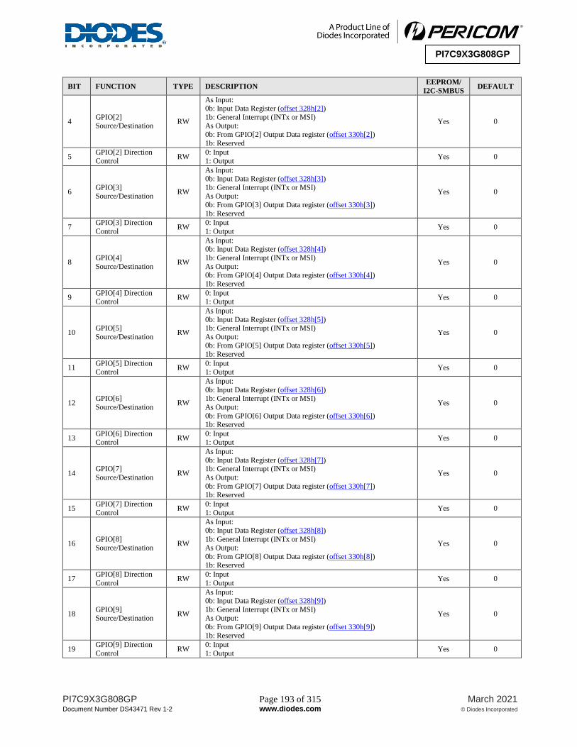
PI7C9X3G808GP Page 193 of 315 March 2021
Document Number DS43471 Rev 1-2 www.diodes.com © Diodes Incorporated
PI7C9X3G808GP
BIT FUNCTION TYPE DESCRIPTION EEPROM/
I2C-SMBUS DEFAULT
4 GPIO[2] Source/Destination
RW
As Input: 0b: Input Data Register (offset 328h[2])
1b: General Interrupt (INTx or MSI) As Output:
0b: From GPIO[2] Output Data register (offset 330h[2])
1b: Reserved
Yes 0
5 GPIO[2] Direction
Control RW
0: Input
1: Output Yes 0
6 GPIO[3] Source/Destination
RW
As Input: 0b: Input Data Register (offset 328h[3])
1b: General Interrupt (INTx or MSI) As Output:
0b: From GPIO[3] Output Data register (offset 330h[3])
1b: Reserved
Yes 0
7 GPIO[3] Direction
Control RW
0: Input
1: Output Yes 0
8 GPIO[4]
Source/Destination RW
As Input: 0b: Input Data Register (offset 328h[4])
1b: General Interrupt (INTx or MSI)
As Output: 0b: From GPIO[4] Output Data register (offset 330h[4])
1b: Reserved
Yes 0
9 GPIO[4] Direction Control
RW 0: Input 1: Output
Yes 0
10 GPIO[5]
Source/Destination RW
As Input:
0b: Input Data Register (offset 328h[5]) 1b: General Interrupt (INTx or MSI)
As Output:
0b: From GPIO[5] Output Data register (offset 330h[5])
1b: Reserved
Yes 0
11 GPIO[5] Direction Control
RW 0: Input 1: Output
Yes 0
12 GPIO[6]
Source/Destination RW
As Input:
0b: Input Data Register (offset 328h[6]) 1b: General Interrupt (INTx or MSI)
As Output:
0b: From GPIO[6] Output Data register (offset 330h[6]) 1b: Reserved
Yes 0
13 GPIO[6] Direction Control
RW 0: Input 1: Output
Yes 0
14 GPIO[7]
Source/Destination RW
As Input:
0b: Input Data Register (offset 328h[7]) 1b: General Interrupt (INTx or MSI)
As Output:
0b: From GPIO[7] Output Data register (offset 330h[7]) 1b: Reserved
Yes 0
15 GPIO[7] Direction
Control RW
0: Input
1: Output Yes 0
16 GPIO[8] Source/Destination
RW
As Input:
0b: Input Data Register (offset 328h[8])
1b: General Interrupt (INTx or MSI) As Output:
0b: From GPIO[8] Output Data register (offset 330h[8]) 1b: Reserved
Yes 0
17 GPIO[8] Direction
Control RW
0: Input
1: Output Yes 0
18 GPIO[9] Source/Destination
RW
As Input: 0b: Input Data Register (offset 328h[9])
1b: General Interrupt (INTx or MSI) As Output:
0b: From GPIO[9] Output Data register (offset 330h[9])
1b: Reserved
Yes 0
19 GPIO[9] Direction
Control RW
0: Input
1: Output Yes 0

PI7C9X3G808GP Page 194 of 315 March 2021
Document Number DS43471 Rev 1-2 www.diodes.com © Diodes Incorporated
PI7C9X3G808GP
BIT FUNCTION TYPE DESCRIPTION EEPROM/
I2C-SMBUS DEFAULT
20 GPIO[10] Source/Destination
RW
As Input: 0b: Input Data Register (offset 328h[10])
1b: General Interrupt (INTx or MSI) As Output:
0b: From GPIO[10] Output Data register (offset 330h[10])
1b: Reserved
Yes 0
21 GPIO[10] Direction
Control RW
0: Input
1: Output Yes 0
22 GPIO[11] Source/Destination
RW
As Input: 0b: Input Data Register (offset 328h[11])
1b: General Interrupt (INTx or MSI) As Output:
0b: From GPIO[11] Output Data register (offset 330h[11])
1b: Reserved
Yes 0
23 GPIO[11] Direction
Control RW
0: Input
1: Output Yes 0
24 GPIO[12]
Source/Destination RW
As Input: 0b: Input Data Register (offset 328h[12])
1b: General Interrupt (INTx or MSI)
As Output: 0b: From GPIO[12] Output Data register (offset 330h[12])
1b: Reserved
Yes 0
25 GPIO[12] Direction Control
RW 0: Input 1: Output
Yes 0
26 GPIO[13]
Source/Destination RW
As Input:
0b: Input Data Register (offset 328h[13]) 1b: General Interrupt (INTx or MSI)
As Output:
0b: From GPIO[13] Output Data register (offset 330h[13])
1b: Reserved
Yes 0
27 GPIO[13] Direction Control
RW 0: Input 1: Output
Yes 0
28 GPIO[14]
Source/Destination RW
As Input:
0b: Input Data Register (offset 328h[14]) 1b: General Interrupt (INTx or MSI)
As Output:
0b: From GPIO[14] Output Data register (offset 330h[14]) 1b: Reserved
Yes 0
29 GPIO[14] Direction Control
RW 0: Input 1: Output
Yes 0
30 GPIO[15]
Source/Destination RW
As Input:
0b: Input Data Register (offset 328h[15]) 1b: General Interrupt (INTx or MSI)
As Output:
0b: From GPIO[15] Output Data register (offset 330h[15]) 1b: Reserved
Yes 0
31 GPIO[15] Direction
Control RW
0: Input
1: Output Yes 0
9.4.101 GPIO 16-31 DIRECTION CONTROL REGISTER – OFFSET 320h (Port 0 Only)
BIT FUNCTION TYPE DESCRIPTION EEPROM/
I2C-SMBUS DEFAULT
0 GPIO[16] Source/Destination
RW
As Input:
0b: Input Data Register (offset 32Ch[0])
1b: General Interrupt (INTx or MSI) As Output:
0b: From GPIO[16] Output Data register (offset 334h[0]) 1b: Reserved
Yes 0
1 GPIO[16] Direction
Control RW
0: Input
1: Output Yes 0

PI7C9X3G808GP Page 195 of 315 March 2021
Document Number DS43471 Rev 1-2 www.diodes.com © Diodes Incorporated
PI7C9X3G808GP
BIT FUNCTION TYPE DESCRIPTION EEPROM/
I2C-SMBUS DEFAULT
2 GPIO[17] Source/Destination
RW
As Input: 0b: Input Data Register (offset 330h[1])
1b: General Interrupt (INTx or MSI) As Output:
0b: From GPIO[17] Output Data register (offset 334h[1])
1b: Reserved
Yes 0
3 GPIO[17] Direction
Control RW
0: Input
1: Output Yes 0
4 GPIO[18] Source/Destination
RW
As Input: 0b: Input Data Register (offset 330h[2])
1b: General Interrupt (INTx or MSI) As Output:
0b: From GPIO[18] Output Data register (offset 334h[2])
1b: Reserved
Yes 0
5 GPIO[18] Direction
Control RW
0: Input
1: Output Yes 0
6 GPIO[19]
Source/Destination RW
As Input: 0b: Input Data Register (offset 330h[3])
1b: General Interrupt (INTx or MSI)
As Output: 0b: From GPIO[19] Output Data register (offset 334h[3])
1b: Reserved
Yes 0
7 GPIO[19] Direction Control
RW 0: Input 1: Output
Yes 0
8 GPIO[20]
Source/Destination RW
As Input:
0b: Input Data Register (offset 330h[4]) 1b: General Interrupt (INTx or MSI)
As Output:
0b: From GPIO[20] Output Data register (offset 334h[4])
1b: Reserved
Yes 0
9 GPIO[20] Direction Control
RW 0: Input 1: Output
Yes 0
10 GPIO[21]
Source/Destination RW
As Input:
0b: Input Data Register (offset 330h[5]) 1b: General Interrupt (INTx or MSI)
As Output:
0b: From GPIO[21] Output Data register (offset 334h[5]) 1b: Reserved
Yes 0
11 GPIO[21] Direction Control
RW 0: Input 1: Output
Yes 0
12 GPIO[22]
Source/Destination RW
As Input:
0b: Input Data Register (offset 330h[6]) 1b: General Interrupt (INTx or MSI)
As Output:
0b: From GPIO[22] Output Data register (offset 334h[6]) 1b: Reserved
Yes 0
13 GPIO[22] Direction
Control RW
0: Input
1: Output Yes 0
14 GPIO[23] Source/Destination
RW
As Input:
0b: Input Data Register (offset 330h[7])
1b: General Interrupt (INTx or MSI) As Output:
0b: From GPIO[23] Output Data register (offset 334h[7]) 1b: Reserved
Yes 0
15 GPIO[23] Direction
Control RW
0: Input
1: Output Yes 0
16 GPIO[24] Source/Destination
RW
As Input: 0b: Input Data Register (offset 330h[8])
1b: General Interrupt (INTx or MSI) As Output:
0b: From GPIO[24] Output Data register (offset 334h[8])
1b: Reserved
Yes 0
17 GPIO[24] Direction
Control RW
0: Input
1: Output Yes 0
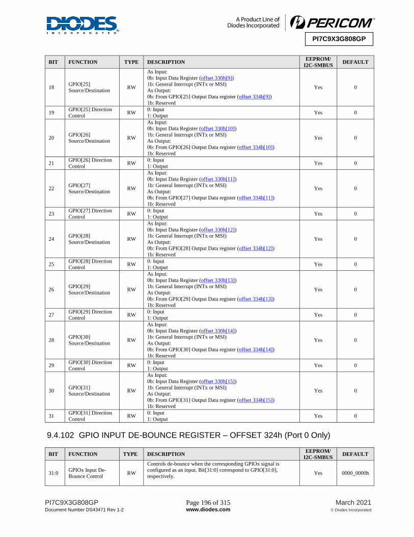
PI7C9X3G808GP Page 196 of 315 March 2021
Document Number DS43471 Rev 1-2 www.diodes.com © Diodes Incorporated
PI7C9X3G808GP
BIT FUNCTION TYPE DESCRIPTION EEPROM/
I2C-SMBUS DEFAULT
18 GPIO[25] Source/Destination
RW
As Input: 0b: Input Data Register (offset 330h[9])
1b: General Interrupt (INTx or MSI) As Output:
0b: From GPIO[25] Output Data register (offset 334h[9])
1b: Reserved
Yes 0
19 GPIO[25] Direction
Control RW
0: Input
1: Output Yes 0
20 GPIO[26] Source/Destination
RW
As Input: 0b: Input Data Register (offset 330h[10])
1b: General Interrupt (INTx or MSI) As Output:
0b: From GPIO[26] Output Data register (offset 334h[10])
1b: Reserved
Yes 0
21 GPIO[26] Direction
Control RW
0: Input
1: Output Yes 0
22 GPIO[27]
Source/Destination RW
As Input: 0b: Input Data Register (offset 330h[11])
1b: General Interrupt (INTx or MSI)
As Output: 0b: From GPIO[27] Output Data register (offset 334h[11])
1b: Reserved
Yes 0
23 GPIO[27] Direction Control
RW 0: Input 1: Output
Yes 0
24 GPIO[28]
Source/Destination RW
As Input:
0b: Input Data Register (offset 330h[12]) 1b: General Interrupt (INTx or MSI)
As Output:
0b: From GPIO[28] Output Data register (offset 334h[12])
1b: Reserved
Yes 0
25 GPIO[28] Direction Control
RW 0: Input 1: Output
Yes 0
26 GPIO[29]
Source/Destination RW
As Input:
0b: Input Data Register (offset 330h[13]) 1b: General Interrupt (INTx or MSI)
As Output:
0b: From GPIO[29] Output Data register (offset 334h[13]) 1b: Reserved
Yes 0
27 GPIO[29] Direction Control
RW 0: Input 1: Output
Yes 0
28 GPIO[30]
Source/Destination RW
As Input:
0b: Input Data Register (offset 330h[14]) 1b: General Interrupt (INTx or MSI)
As Output:
0b: From GPIO[30] Output Data register (offset 334h[14]) 1b: Reserved
Yes 0
29 GPIO[30] Direction
Control RW
0: Input
1: Output Yes 0
30 GPIO[31] Source/Destination
RW
As Input:
0b: Input Data Register (offset 330h[15])
1b: General Interrupt (INTx or MSI) As Output:
0b: From GPIO[31] Output Data register (offset 334h[15]) 1b: Reserved
Yes 0
31 GPIO[31] Direction
Control RW
0: Input
1: Output Yes 0
9.4.102 GPIO INPUT DE-BOUNCE REGISTER – OFFSET 324h (Port 0 Only)
BIT FUNCTION TYPE DESCRIPTION EEPROM/
I2C-SMBUS DEFAULT
31:0 GPIOx Input De-
Bounce Control RW
Controls de-bounce when the corresponding GPIOx signal is configured as an input. Bit[31:0] correspond to GPIO[31:0],
respectively.
Yes 0000_0000h

PI7C9X3G808GP Page 197 of 315 March 2021
Document Number DS43471 Rev 1-2 www.diodes.com © Diodes Incorporated
PI7C9X3G808GP
BIT FUNCTION TYPE DESCRIPTION EEPROM/
I2C-SMBUS DEFAULT
0b: GPIOx input is not de-bounced 1b: GPIOx input is de-bounced
9.4.103 GPIO 0-15 INPUT DATA REGISTER – OFFSET 328h (Port 0 Only)
BIT FUNCTION TYPE DESCRIPTION EEPROM/
I2C-SMBUS DEFAULT
0 GPIO[0] Input Data RW
GPIO[0] Input Data
Return 0 if GPIO[0] is configured as an output (offset 31Ch[1]=1) Return the state of GPIO[0] pin if GPIO[0] is configured as an input
(offset 31Ch[1]=0)
Yes 1
1 GPIO[1] Input Data RW
GPIO[1] Input Data Return 0 if GPIO[1] is configured as an output (offset 31Ch[3]=1)
Return the state of GPIO[1] pin if GPIO[1] is configured as an input (offset 31Ch[3]=0)
Yes 1
2 GPIO[2] Input Data RW
GPIO[2] Input Data
Return 0 if GPIO[2] is configured as an output (offset 31Ch[5]=1) Return the state of GPIO[2] pin if GPIO[2] is configured as an input
(offset 31Ch[5]=0)
Yes 0
3 GPIO[3] Input Data RW
GPIO[3] Input Data Return 0 if GPIO[3] is configured as an output (offset 31Ch[7]=1)
Return the state of GPIO[3] pin if GPIO[3] is configured as an input (offset 31Ch[7]=0)
Yes 1
4 GPIO[4] Input Data RW
GPIO[4] Input Data
Return 0 if GPIO[4] is configured as an output (offset 31Ch[9]=1) Return the state of GPIO[4] pin if GPIO[4] is configured as an input
(offset 31Ch[9]=0)
Yes 0
5 GPIO[5] Input Data RW
GPIO[5] Input Data Return 0 if GPIO[5] is configured as an output (offset 31Ch[11]=1)
Return the state of GPIO[5] pin if GPIO[5] is configured as an input
(offset 31Ch[11]=0)
Yes 1
6 GPIO[6] Input Data RW
GPIO[6] Input Data
Return 0 if GPIO[6] is configured as an output (offset 31Ch[13]=1)
Return the state of GPIO[6] pin if GPIO[6] is configured as an input (offset 31Ch[13]=0)
Yes 0
7 GPIO[7] Input Data RW
GPIO[7] Input Data
Return 0 if GPIO[7] is configured as an output (offset 31Ch[15]=1) Return the state of GPIO[7] pin if GPIO[7] is configured as an input
(offset 31Ch[15]=0)
Yes 1
8 GPIO[8] Input Data RW
GPIO[8] Input Data Return 0 if GPIO[8] is configured as an output (offset 31Ch[17]=1)
Return the state of GPIO[8] pin if GPIO[8] is configured as an input (offset 31Ch[17]=0)
Yes 0
9 GPIO[9] Input Data RW
GPIO[9] Input Data
Return 0 if GPIO[9] is configured as an output (offset 31Ch[19]=1) Return the state of GPIO[9] pin if GPIO[9] is configured as an input
(offset 31Ch[19]=0)
Yes 1
10 GPIO[10] Input Data RW
GPIO[10] Input Data Return 0 if GPIO[10] is configured as an output (offset 31Ch[21]=1)
Return the state of GPIO[10] pin if GPIO[10] is configured as an input (offset 31Ch[21]=0)
Yes 0
11 GPIO[11] Input Data RW
GPIO[11] Input Data
Return 0 if GPIO[11] is configured as an output (offset 31Ch[23]=1) Return the state of GPIO[11] pin if GPIO[11] is configured as an
input (offset 31Ch[23]=0)
Yes 1
12 GPIO[12] Input Data RW
GPIO[12] Input Data Return 0 if GPIO[12] is configured as an output (offset 31Ch[25]=1)
Return the state of GPIO[12] pin if GPIO[12] is configured as an
input (offset 31Ch[25]=0)
Yes 0
13 GPIO[13] Input Data RW
GPIO[13] Input Data
Return 0 if GPIO[13] is configured as an output (offset 31Ch[27]=1)
Return the state of GPIO[13] pin if GPIO[13] is configured as an input (offset 31Ch[27]=0)
Yes 1

PI7C9X3G808GP Page 198 of 315 March 2021
Document Number DS43471 Rev 1-2 www.diodes.com © Diodes Incorporated
PI7C9X3G808GP
BIT FUNCTION TYPE DESCRIPTION EEPROM/
I2C-SMBUS DEFAULT
14 GPIO[14] Input Data RW
GPIO[14] Input Data Return 0 if GPIO[14] is configured as an output (offset 31Ch[29]=1)
Return the state of GPIO[11] pin if GPIO[11] is configured as an input (offset 31Ch[29]=0)
Yes 0
15 GPIO[15] Input Data RW
GPIO[15] Input Data
Return 0 if GPIO[15] is configured as an output (offset 31Ch[31]=1) Return the state of GPIO[15] pin if GPIO[15] is configured as an
input (offset 31Ch[31]=0)
Yes 1
31:16 Reserved RsvdP Not support. No 0000h
9.4.104 GPIO 16-31 INPUT DATA REGISTER – OFFSET 32Ch (Port 0 Only)
BIT FUNCTION TYPE DESCRIPTION EEPROM/
I2C-SMBUS DEFAULT
0 GPIO[16] Input Data RO
GPIO[16] Input Data
Return 0 if GPIO[16] is configured as an output (offset 320h[1]=1)
Return the state of GPIO[16] pin if GPIO[16] is configured as an input (offset 320h[1]=0)
Yes 0
1 GPIO[17] Input Data RO
GPIO[17] Input Data
Return 0 if GPIO[17] is configured as an output (offset 320h[3]=1) Return the state of GPIO[17] pin if GPIO[17] is configured as an
input (offset 320h[3]=0)
Yes 1
2 GPIO[18] Input Data RO
GPIO[18] Input Data Return 0 if GPIO[18] is configured as an output (offset 320h[5]=1)
Return the state of GPIO[18] pin if GPIO[18] is configured as an input (offset 320h[5]=0)
Yes 0
3 GPIO[19] Input Data RO
GPIO[19] Input Data
Return 0 if GPIO[19] is configured as an output (offset 320h[7]=1) Return the state of GPIO[19] pin if GPIO[19] is configured as an
input (offset 320h[7]=0)
Yes 1
4 GPIO[20] Input Data RO
GPIO[20] Input Data Return 0 if GPIO[20] is configured as an output (offset 320h[9]=1)
Return the state of GPIO[20] pin if GPIO[20] is configured as an
input (offset 320h[9]=0)
Yes 0
5 GPIO[21] Input Data RO
GPIO[21] Input Data
Return 0 if GPIO[21] is configured as an output (offset 320h[11]=1)
Return the state of GPIO[21] pin if GPIO[21] is configured as an input (offset 320h[11]=0)
Yes 1
6 GPIO[22] Input Data RO
GPIO[22] Input Data
Return 0 if GPIO[22] is configured as an output (offset 320h[13]=1) Return the state of GPIO[22] pin if GPIO[22] is configured as an
input (offset 320h[13]=0)
Yes 0
7 GPIO[23] Input Data RO
GPIO[23] Input Data
Return 0 if GPIO[23] is configured as an output (offset 320h[15]=1)
Return the state of GPIO[23] pin if GPIO[23] is configured as an input (offset 320h[15]=0)
Yes 1
8 GPIO[24] Input Data RO
GPIO[24] Input Data
Return 0 if GPIO[24] is configured as an output (offset 320h[17]=1) Return the state of GPIO[24] pin if GPIO[24] is configured as an
input (offset 320h[17]=0)
Yes 0
9 GPIO[25] Input Data RO
GPIO[25] Input Data Return 0 if GPIO[25] is configured as an output (offset 320h[19]=1)
Return the state of GPIO[25] pin if GPIO[25] is configured as an input (offset 320h[19]=0)
Yes 1
10 GPIO[26] Input Data RO
GPIO[26] Input Data
Return 0 if GPIO[26] is configured as an output (offset 320h[21]=1) Return the state of GPIO[26] pin if GPIO[26] is configured as an
input (offset 320h[21]=0)
Yes 0
11 GPIO[27] Input Data RO
GPIO[27] Input Data
Return 0 if GPIO[27] is configured as an output (offset 320h[23]=1)
Return the state of GPIO[27] pin if GPIO[27] is configured as an
input (offset 320h[23]=0)
Yes 1

PI7C9X3G808GP Page 199 of 315 March 2021
Document Number DS43471 Rev 1-2 www.diodes.com © Diodes Incorporated
PI7C9X3G808GP
BIT FUNCTION TYPE DESCRIPTION EEPROM/
I2C-SMBUS DEFAULT
12 GPIO[28] Input Data RO
GPIO[28] Input Data Return 0 if GPIO[28] is configured as an output (offset 320h[25]=1)
Return the state of GPIO[28] pin if GPIO[28] is configured as an input (offset 320h[25]=0)
Yes 0
13 GPIO[29] Input Data RO
GPIO[29] Input Data
Return 0 if GPIO[29] is configured as an output (offset 320h[27]=1) Return the state of GPIO[29] pin if GPIO[29] is configured as an
input (offset 320h[27]=0)
Yes 1
14 GPIO[30] Input Data RO
GPIO[30] Input Data Return 0 if GPIO[30] is configured as an output (offset 320h[29]=1)
Return the state of GPIO[30] pin if GPIO[30] is configured as an input (offset 320h[29]=0)
Yes 0
15 GPIO[31] Input Data RO
GPIO[31] Input Data
Return 0 if GPIO[31] is configured as an output (offset 320h[31]=1) Return the state of GPIO[31] pin if GPIO[31] is configured as an
input (offset 320h[31]=0)
Yes 1
31:16 Reserved RsvdP Not support. No 0000h
9.4.105 GPIO 0-15 OUTPUT DATA REGISTER – OFFSET 330h (Port 0 Only)
BIT FUNCTION TYPE DESCRIPTION EEPROM/
I2C-SMBUS DEFAULT
0 GPIO[0] Output Data RW GPIO[0] Output Data The value written to this bit is driven to GPIO[0] output if GPIO[0]
is configured as an output (offset 31Ch[1]=1)
Yes 0
1 GPIO[1] Output Data RW GPIO[1] Output Data The value written to this bit is driven to GPIO[1] output if GPIO[1]
is configured as an output (offset 31Ch[3]=1)
Yes 0
2 GPIO[2] Output Data RW GPIO[2] Output Data The value written to this bit is driven to GPIO[2] output if GPIO[2]
is configured as an output (offset 31Ch[5]=1)
Yes 0
3 GPIO[3] Output Data RW GPIO[3] Output Data The value written to this bit is driven to GPIO[3] output if GPIO[3]
is configured as an output (offset 31Ch[7]=1)
Yes 0
4 GPIO[4] Output Data RW GPIO[4] Output Data The value written to this bit is driven to GPIO[4] output if GPIO[4]
is configured as an output (offset 31Ch[9]=1)
Yes 0
5 GPIO[5] Output Data RW
GPIO[5] Output Data
The value written to this bit is driven to GPIO[5] output if GPIO[5]
is configured as an output (offset 31Ch[11]=1)
Yes 0
6 GPIO[6] Output Data RW
GPIO[6] Output Data
The value written to this bit is driven to GPIO[6] output if GPIO[6]
is configured as an output (offset 31Ch[13]=1)
Yes 0
7 GPIO[7] Output Data RW
GPIO[7] Output Data
The value written to this bit is driven to GPIO[7] output if GPIO[7]
is configured as an output (offset 31Ch[15]=1)
Yes 0
8 GPIO[8] Output Data RW
GPIO[8] Output Data
The value written to this bit is driven to GPIO[8] output if GPIO[8]
is configured as an output (offset 31Ch[17]=1)
Yes 0
9 GPIO[9] Output Data RW
GPIO[9] Output Data
The value written to this bit is driven to GPIO[9] output if GPIO[9]
is configured as an output (offset 31Ch[19]=1)
Yes 0
10 GPIO[10] Output Data
RW
GPIO[10] Output Data
The value written to this bit is driven to GPIO[10] output if
GPIO[10] is configured as an output (offset 31Ch[21]=1)
Yes 0
11 GPIO[11] Output Data
RW
GPIO[11] Output Data
The value written to this bit is driven to GPIO[11] output if GPIO[11] is configured as an output (offset 31Ch[23]=1)
Yes 0
12 GPIO[12] Output Data
RW
GPIO[12] Output Data
The value written to this bit is driven to GPIO[12] output if GPIO[12] is configured as an output (offset 31Ch[25]=1)
Yes 0
13 GPIO[13] Output Data
RW
GPIO[13] Output Data
The value written to this bit is driven to GPIO[13] output if GPIO[13] is configured as an output (offset 31Ch[27]=1)
Yes 0

PI7C9X3G808GP Page 200 of 315 March 2021
Document Number DS43471 Rev 1-2 www.diodes.com © Diodes Incorporated
PI7C9X3G808GP
BIT FUNCTION TYPE DESCRIPTION EEPROM/
I2C-SMBUS DEFAULT
14 GPIO[14] Output Data
RW GPIO[14] Output Data The value written to this bit is driven to GPIO[14] output if
GPIO[14] is configured as an output (offset 31Ch[29]=1)
Yes 0
15 GPIO[15] Output Data
RW GPIO[15] Output Data The value written to this bit is driven to GPIO[15] output if
GPIO[15] is configured as an output (offset 31Ch[31]=1)
Yes 0
31:16 Reserved RsvdP Not support. No 0000h
9.4.106 GPIO 16-31 OUTPUT DATA REGISTER – OFFSET 334h (Port 0 Only)
BIT FUNCTION TYPE DESCRIPTION EEPROM/
I2C-SMBUS DEFAULT
0 GPIO[16] Output Data
RW
GPIO[16] Output Data
The value written to this bit is driven to GPIO[16] output if GPIO[16] is configured as an output (offset 320h[1]=1)
Yes 0
1 GPIO[17] Output Data
RW
GPIO[17] Output Data
The value written to this bit is driven to GPIO[17] output if GPIO[17] is configured as an output (offset 320h[3]=1)
Yes 0
2 GPIO[18] Output Data
RW
GPIO[18] Output Data
The value written to this bit is driven to GPIO[18] output if GPIO[18] is configured as an output (offset 320h[5]=1)
Yes 0
3 GPIO[19] Output
Data RW
GPIO[19] Output Data
The value written to this bit is driven to GPIO[19] output if GPIO[19] is configured as an output (offset 320h[7]=1)
Yes 0
4 GPIO[20] Output
Data RW
GPIO[20] Output Data
The value written to this bit is driven to GPIO[20] output if GPIO[20] is configured as an output (offset 320h[9]=1)
Yes 0
5 GPIO[21] Output
Data RW
GPIO[21] Output Data
The value written to this bit is driven to GPIO[21] output if GPIO[21] is configured as an output (offset 320h[11]=1)
Yes 0
6 GPIO[22] Output
Data RW
GPIO[22] Output Data
The value written to this bit is driven to GPIO[22] output if GPIO[22] is configured as an output (offset 320h[13]=1)
Yes 0
7 GPIO[23] Output
Data RW
GPIO[23] Output Data
The value written to this bit is driven to GPIO[23] output if GPIO[23] is configured as an output (offset 320h[15]=1)
Yes 0
8 GPIO[24] Output
Data RW
GPIO[24] Output Data
The value written to this bit is driven to GPIO[24] output if GPIO[24] is configured as an output (offset 320h[17]=1)
Yes 0
9 GPIO[25] Output
Data RW
GPIO[25] Output Data
The value written to this bit is driven to GPIO[25] output if GPIO[25] is configured as an output (offset 320h[19]=1)
Yes 0
10 GPIO[26] Output
Data RW
GPIO[26] Output Data
The value written to this bit is driven to GPIO[26] output if GPIO[26] is configured as an output (offset 320h[21]=1)
Yes 0
11 GPIO[27] Output
Data RW
GPIO[27] Output Data
The value written to this bit is driven to GPIO[27] output if GPIO[27] is configured as an output (offset 320h[23]=1)
Yes 0
12 GPIO[28] Output
Data RW
GPIO[28] Output Data
The value written to this bit is driven to GPIO[28] output if GPIO[28] is configured as an output (offset 320h[25]=1)
Yes 0
13 GPIO[29] Output
Data RW
GPIO[29] Output Data The value written to this bit is driven to GPIO[29] output if
GPIO[29] is configured as an output (offset 320h[27]=1)
Yes 0
14 GPIO[30] Output
Data RW
GPIO[30] Output Data The value written to this bit is driven to GPIO[30] output if
GPIO[30] is configured as an output (offset 320h[29]=1)
Yes 0
15 GPIO[31] Output
Data RW
GPIO[31] Output Data
The value written to this bit is driven to GPIO[31] output if
GPIO[31] is configured as an output (offset 320h[31]=1)
Yes 0
31:16 Reserved RsvdP Not support. No 0000h

PI7C9X3G808GP Page 201 of 315 March 2021
Document Number DS43471 Rev 1-2 www.diodes.com © Diodes Incorporated
PI7C9X3G808GP
9.4.107 GPIO 0-31 INTERRUPT POLARITY REGISTER – OFFSET 338h (Port 0 Only)
BIT FUNCTION TYPE DESCRIPTION EEPROM/
I2C-SMBUS DEFAULT
31:0 GPIO Interrupt
Polarity RW
Controls whether GPIO Interrupt input is Active-Low or Active-
High for the corresponding GPIOx signal. Bit[31:0] correspond to GPIO[31:0], respectively.
0b: GPIO Interrupt input is Active-Low
1b: GPIO Interrupt input is Active-High
Yes 0000_0000h
9.4.108 GPIO 0-31 INTERRUPT STATUS REGISTER – OFFSET 33Ch (Port 0 Only)
BIT FUNCTION TYPE DESCRIPTION EEPROM/
I2C-SMBUS DEFAULT
31:0 GPIO Interrupt
Status RO
Indicates whether GPIO interrupt are inactive or active for the corresponding GPIOx signal. Bit[31:0] correspond to GPIO[31:0]
respectively.
0b: GPIO interrupt is inactive
1b: GPIO interrupt is active
No 0000_0000h
9.4.109 GPIO 0-31 INTERRUPT MASK REGISTER – OFFSET 340h (Port 0 Only)
BIT FUNCTION TYPE DESCRIPTION EEPROM/
I2C-SMBUS DEFAULT
31:0 GPIO Interrupt Mask RW
Indicates whether GPIO interrupts are masked or not masked for the corresponding GPIOx signal. Bit[31:0] correspond to GPIO[31:0],
respectively.
0b: GPIO interrupt is unmasked
1b: GPIO interrupt is masked
Yes 0000_0000h
9.4.110 OPERATION MODE REGISTER – OFFSET 348h (Port 0 Only)
BIT FUNCTION TYPE DESCRIPTION EEPROM/
I2C-SMBUS DEFAULT
2:0 Reserved RsvdP Not support. No 000b
5:3 pkgsel RO Package Bonding option. No 000b
8:6 portcfg RO
Port/lane configuration settins. They are decided by the status of
PORTCFG[2:0] strap pins 001b: 2 x4 ports 010b: 1 x4, 2 x2 ports
011b: 4 x2 ports 100b: 1 x4, 4 x1 ports
101b: 8 x1 ports
Others: Reserved
No
Set by
PORTCFG [2:0]
10:9 chipmode RO
Chip operation mode selection. They are decided by the status of
CHIPMODE[2:0] strap pins.
00b: Normal mode
01b: iddq/mbist mode 10b: AC JTAG mode
11b: phy_mode
No 00b
12:11 Reserved RsvdP Not support. No 00b
13 ckmode RO
Reference clock modes. It is decided by the status of CKMODE
strap pin.
0b: base mode
1b: CDEP separate reference mode
No 0b
14 dma_mode RO 0b: disable DMA
1b: enable DMA No 0

PI7C9X3G808GP Page 202 of 315 March 2021
Document Number DS43471 Rev 1-2 www.diodes.com © Diodes Incorporated
PI7C9X3G808GP
BIT FUNCTION TYPE DESCRIPTION EEPROM/
I2C-SMBUS DEFAULT
20:15 upport_sel RO Upstream port selection. No 0000_00b
21 CDEP_mode RO 0b: disable CDEP
1b: enable CDEP No 0
22 scan_tm RO 0b: normal mode 1b: scan mode
No 0
23 hotplug_pin_en RO
It is decided by the status of HOT_PLUG_EN_L strap pin.
0b: GPIO[31:0] are GPIO pins
1b: GPIO[31:0] are used as hot plug pins
No 1
24 surprise_hp_en RO
It is decided by the status of SURPRISE_HP strap pin.
0b: disable surprise hot-plug
1b: enable surprise hot-plug
No 0
25 ioe_40bit_en RO 0b: support 16 bit IOE
1b: support 40 bit IOE No 0
26 clkbuf_pd RO
It is decided by the status of CLKBUFPD_L strap pin.
0b: clock buffer is in normal mode 1b: clock buffer is in power down mode
No 1
27 pm_l1_1_en RO
It is decided by the status of PM_L11_EN_L strap pin.
0b: GPIO[15:8] are GPIO pins
1b: GPIO[15:8] are used as CLKREQ_L[7:0]
No
Set by
PM_L11_EN_
L
30:28 i2c/smaddr_out RO Indicate I2C/SMBUS address[2:0]. No Set by
I2C_ADDRES
[2:0]
31 Reserved RsvdP Not Support. No 1
9.4.111 CLOCK BUFFER CONTROL REGISTER – OFFSET 34Ch (Port 0 Only)
BIT FUNCTION TYPE DESCRIPTION EEPROM/
I2C-SMBUS DEFAULT
7:0 Clock OE Control RW 0b… disable clock output
1b… enable clock output Yes FFh
8 Clock Power Down RW
Used to set CLKBUFPD_L strap pin.
0b… power on
1b… power down
Yes 0
9 Control Enable RW 0b… disable to use this register control clock buffer output
1b… enable to use this register control clock buffer output Yes 0
10 Clock Source Sel RW 0b… input clock buffer source is from differential clock pad 1b… input clock buffer source is from CMOS single end clock
source
Yes 0
23:11 Reserved RsvdP Not support. No 0_0h
31:24 Revision ID RO Revision id. No 00h
9.4.112 LTSSM CSR 0 REGISTER – OFFSET 380h
BIT FUNCTION TYPE DESCRIPTION EEPROM/
I2C-SMBUS DEFAULT
3:0 eq_preset_uplimited_
0 RW
Define EQ evaluate upper limiter range of preset. This value is
defined per lane. Yes Ah
7:4 eq_preset_dnlimited_0
RW Define EQ evaluate down limiter range of preset. This value is defined per lane.
Yes 5h
11:8 eq_preset_uplimited_
1 RW
Define EQ evaluate upper limiter range of preset. This value is
defined per lane. Yes Ah
15:12 eq_preset_dnlimited_
1 RW
Define EQ evaluate down limiter range of preset. This value is
defined per lane. Yes 5h
19:16 eq_preset_uplimited_2
RW Define EQ evaluate upper limiter range of preset. This value is defined per lane.
Yes Ah
23:20 eq_preset_dnlimited_
2 RW
Define EQ evaluate down limiter range of preset. This value is
defined per lane. Yes 5h

PI7C9X3G808GP Page 203 of 315 March 2021
Document Number DS43471 Rev 1-2 www.diodes.com © Diodes Incorporated
PI7C9X3G808GP
BIT FUNCTION TYPE DESCRIPTION EEPROM/
I2C-SMBUS DEFAULT
27:24 eq_preset_uplimited_3
RW Define EQ evaluate upper limiter range of preset. This value is defined per lane.
Yes Ah
31:28 eq_preset_dnlimited_
3 RW
Define EQ evaluate down limiter range of preset. This value is
defined per lane. Yes 5h
9.4.113 LTSSM CSR 1 REGISTER – OFFSET 384h
BIT FUNCTION TYPE DESCRIPTION EEPROM/
I2C-SMBUS DEFAULT
31:0 Reserved RsvdP Not support. No 5A5A_5A5Ah
9.4.114 LTSSM CSR 2 REGISTER – OFFSET 388h
BIT FUNCTION TYPE DESCRIPTION EEPROM/
I2C-SMBUS DEFAULT
3:0 eq_preset_uplimited_
4 RW
Define EQ evaluate upper limiter range of preset. This value is
defined per lane. Yes Ah
7:4 eq_preset_dnlimited_
4 RW
Define EQ evaluate down limiter range of preset. This value is
defined per lane. Yes 5h
11:8 eq_preset_uplimited_5
RW Define EQ evaluate upper limiter range of preset. This value is defined per lane.
Yes Ah
15:12 eq_preset_dnlimited_
5 RW
Define EQ evaluate down limiter range of preset. This value is
defined per lane. Yes 5h
19:16 eq_preset_uplimited_6
RW Define EQ evaluate upper limiter range of preset. This value is defined per lane.
Yes Ah
23:20 eq_preset_dnlimited_
6 RW
Define EQ evaluate down limiter range of preset. This value is
defined per lane. Yes 5h
27:24 eq_preset_uplimited_
7 RW
Define EQ evaluate upper limiter range of preset. This value is
defined per lane. Yes Ah
31:28 eq_preset_dnlimited_7
RW Define EQ evaluate down limiter range of preset. This value is defined per lane.
Yes 5h
9.4.115 LTSSM CSR 3 REGISTER – OFFSET38Ch
BIT FUNCTION TYPE DESCRIPTION EEPROM/
I2C-SMBUS DEFAULT
31:0 Reserved RsvdP Not support. No 5A5A_5A5Ah
9.4.116 LTSSM 0 REGISTER – OFFSET 390h
BIT FUNCTION TYPE DESCRIPTION EEPROM/
I2C-SMBUS DEFAULT
1:0 det_times RW Used to set how many detect times will LTSSM execute. Max
times =3 and Mini times is 1. Yes 11b
2 force2detect RW Force LTSSM state stay in detect state. Yes 0
3 force2compliance RW Force LTSSM send compliance pattern. Yes 0
5:4 force_comp_rate RW Force LTSSM compliance in forced compliance mode. Yes 00b
9:6 force_comp_deep_ preset
RW Force LTSSM GEN3 compliance mode’s preset value. Yes 0h
10 comp_parity_en RW Force GEN 1/GEN2 compliance parity. Debug only. Yes 0
11 force2loop RW Force LTSSM to loopback mode Yes 0
12 upconfig_capable RW Enable upconfig capability Yes 0
13 lane_disable RW 1: lane will be disable when it is a unused lane. Yes 0
17:14 sh_reset_time_sel RW
Assert reset period on hot plug power on/power off sequence.
00b: 100 ms
01b: 300 ms 10b: 500 ms
11b: 600 ms
Yes 3h
19:18 Reserved RsvdP Not support. No 00b
27:20 tx_nfts_num RW NFTS NUMBER. Yes F0h

PI7C9X3G808GP Page 204 of 315 March 2021
Document Number DS43471 Rev 1-2 www.diodes.com © Diodes Incorporated
PI7C9X3G808GP
BIT FUNCTION TYPE DESCRIPTION EEPROM/
I2C-SMBUS DEFAULT
28 Reserved RsvdP Not support. No 0
29 chg_ln_width RW Enable change link width Yes 0
30 up_speed_ctrl_chx RW Enable upstream port speed change when DL_UP in GEN 3 speed. Yes 0
31 ltssm_debug_sel RW 0b: the output of offset 734h is for embedded LA 1b: the output of offset 734h is for LTSSM flow
Yes 1
9.4.117 LTSSM 1 REGISTER – OFFSET 394h
BIT FUNCTION TYPE DESCRIPTION EEPROM/
I2C-SMBUS DEFAULT
1:0 recv_eq_process_sel RW EQ evaluated mode. Debug only. Yes 01b
2 comp_recv_bit_set RW Send compliance receive bit in loopback mode. Yes 0
3 mrlpdc_ctrl_in RW Enable D3 dilink function Yes 0
8:4 eq_eval_time RW Evaluate process timer selection. Debug only. Yes 0_0000b
10:9 mrlpdc_tmr_sel RW When D3 dlink function is enable. This timer set PDC enable time. Yes 00b
11 enter_loop_back RW LOOPBACK master enable. Yes 0
12 infer_eidle_en RW Enable infer eidle function. Yes 1
13 aspm_nack_en RW Enable response NACK Message when ASPM L1 DLLP request. Yes 0
14 Hp_hot_ctr_en_reg RW Force mrlpdc =0. Debug only Yes 0h
15 Hp_hot_clk_en_reg RW Enable clock buffer. Colock do not control by SHP control. Yes 0h
19:16 Reserved RsvdP Not support. No 0_0b
22:20 any_phy_sts RW Control physts align time. Internal used only. Yes 0
31:24 ltssm_debug_sel RW Internal used only. Yes 00h
9.4.118 LTSSM 2 REGISTER – OFFSET 398h
BIT FUNCTION TYPE DESCRIPTION EEPROM/
I2C-SMBUS DEFAULT
15:0 detect_timer_sel RW Define two ltssmtxdetect space. Debug only Yes 0000h
23:16 sel_linkevalfigure RW Set good FOM value threshold Yes F0h
26:24 lane_good_sel RW
Selection lane good condition.
00b: coefficient do not need change
01b: FOM!=00b and coefficient did not need change 10b: FOM=threshold or coefficient did not need change
11b: FOM=threshold and coefficient did not need change
Yes 000b
28:27 eidle_sel_reg RW 1b: Use PHY generate electrical 0b: Use internal electrical
Yes 0
29 sh_extra_reset RW Internal used only. Yes 0
30 ioe_addr_sel RW
Use register setting register to match outside IOE address.
0b: internal
1b: register setting value
Yes 0
31 Ioe_40 RW 1b: USE 40 pin IOE
0b: Use 16 pin IOE Yes 0
9.4.119 LTSSM 3 REGISTER – OFFSET 39Ch
BIT FUNCTION TYPE DESCRIPTION EEPROM/
I2C-SMBUS DEFAULT
6:0 cfg_address_in RW IOE address defined by register. Yes 00h
7 hp_scl_clk_sel_in RW
I2C clock rate.
0b: 62Khz 1b: 31Khz
Yes 0
15:8 aspm_l1_cnt_num RW Accumulated l0s number to enter ASPM l1 condition. Yes 08h
31:16 aspm_l1 RW ASPM L1 idle timer. Yes 0FFFh

PI7C9X3G808GP Page 205 of 315 March 2021
Document Number DS43471 Rev 1-2 www.diodes.com © Diodes Incorporated
PI7C9X3G808GP
9.4.120 LTSSM 4 REGISTER – OFFSET 3A0h
BIT FUNCTION TYPE DESCRIPTION EEPROM/
I2C-SMBUS DEFAULT
15:0 tx_swing RW TX swing setting by register value. Yes 0000h
17:16 eios_cnt RW Polling compliance exit condition. Yes 1
18 bypass_detect RW Ignore LTSSM detect result and use max lane width. Yes 0
19 detection_option RW 1b: use detection result 0b: use modify detection result
Yes 0
20 stand_by RW
Used to control whether the PHY rx is active when PHY is in P0 or
P0s.
1b: Active
0b: Standby
Yes 0
21 in_progress RW Set rxeqprocess behavior. Internal used only. Yes 0
22 deskew_rxeqval RW Set deskew behavior in EQ period. Internal used only. Yes 0
23 ltssm_cfg2loop_sel RW
Cfg go to loopback condition.
0b : see any loopback bit 1b: see all loopback bit. Internal used only.
Yes 0
27:24 recv_eq_optionl RW
Eq_option.
bit[0]… set eq_valid =1
Yes 001b
31:28 ltssm_cfg_reversal RW Select reversal condition. Internal used only. Yes 0
9.4.121 LTSSM 5 REGISTER – OFFSET 3A4h
BIT FUNCTION TYPE DESCRIPTION EEPROM/
I2C-SMBUS DEFAULT
15:0 tskp_gen1_n0_reg RW When sris support, use this skip value. Yes 004Bh
31:16 skp_gen1_reg RW When sris disable, use the skip value. Yes 0258h
9.4.122 LTSSM 6 REGISTER – OFFSET 3A8h
BIT FUNCTION TYPE DESCRIPTION EEPROM/
I2C-SMBUS DEFAULT
15:0 tskp_gen3_n0_reg RW When sris support, use this skip value. Yes 011Ch
31:16 tskp_gen3_reg RW When sris disable, use the skip value. Yes 0BBEh
9.4.123 LTSSM 7 REGISTER – OFFSET 3ACh
BIT FUNCTION TYPE DESCRIPTION EEPROM/
I2C-SMBUS DEFAULT
4:0 ltssm_rx_mask_reg RW
bit[0]… mask hot reset bit
bit[1]… mask disable bit bit[2]… mask loopback bit
bit[3]… mask disable scrambling bit
bit[4]… mask compliance bit
Yes 0_0000b
5 ltssm_port_split_ctr_
reg RW
0b: enable port split
1b: disable port split Yes 0
9:6 ltssm_lg_idle_cnt_ reg
RW Used to set idle data receive date number. Yes 6h
10 ltssm_chg_rate_ms_
reg RW Used to control down port change rate as a master. Yes 0
11 gpio_in_reg_tmp RW In external I2C IOE bit[6],it is GPIO bit. Yes 0
15:12 ltssm_config_rev_
num_reg RW
bit[1:0]… cfg.linkaccept to cfg.linkwait couter selection.
bit[3:2]… cfg.lanenum to cfg.cpl counter selection Yes 0000b
16 ltssm_config_delay_cnt_reg
RW cfg.start delay time to cfg.linkaccept. Use this delay time to decide partial lane detection.
Yes 0
17 disable_cfg_lane_
chg_reg RW disable cfg.linkaccept state change lane. Yes 0
18 disable_cfg_lane_
time_reg RW disable cfg.lanenum to detect state. Yes 0

PI7C9X3G808GP Page 206 of 315 March 2021
Document Number DS43471 Rev 1-2 www.diodes.com © Diodes Incorporated
PI7C9X3G808GP
BIT FUNCTION TYPE DESCRIPTION EEPROM/
I2C-SMBUS DEFAULT
22:19 partial_lane_sel_reg RW bit[1:0]… decide partial lane reverse bit[2]… reserved
bit[3]… delay cfg.start to cfg.linaccept sate for cross link
Yes 0001b
23 enable_becon_l2_reg RW Used to enable L2 send becon signal. Yes 0
24 Reserved RsvdP Not support. No 0
26:25 lane_change_ctr_reg RW Used to control lane number change in cfg state. Yes 00b
28:27 poll_exit_comp_cnt_reg
RW Used to set poll.compliance exit counter. Yes 11b
29 led_mode_prsnt_sel_
reg RW
Used to select present detect pin come from IOE or IO pin in
surprise mode. Yes 1
30 shp_rest_ctr_reg RW
Used to control ip_core reset pin come from reset_top or shp generation.
0b: come from shp generation
1b: come from reset_top
Yes 0
31 always_wait_linkup_reg
RW In shp control,shp try to link up device always. Yes 0
9.4.124 LTSSM 8 REGISTER – OFFSET 3B0h
BIT FUNCTION TYPE DESCRIPTION EEPROM/
I2C-SMBUS DEFAULT
0 dpc_error_latch RW
When dpc error occurs, ltssm will entry to disable state.
0b: dpc error signal will be latched until ltssm go to disable state.
1b: dpc error signal will not be latched.
Yes 1
1 any_phy_sts_tmp_sel
_reg RW
0b: come from all phy_sts
1b: combine with lane detetion. Yes 0
5:2 cfg_stat_ctr_reg RW cfg_start option selection. Yes 0000b
19:6 rate_chg_ctr_reg RW Used to control rate change behavior. Yes 0-0b
23:20 loop_test_ctr_reg RW loop test behavior control. Yes 0h
25:24 l0_power_dn_wait_ t_reg
RW
When receive/transmitter eios, pm control wait 50 cycle time to
L1/l0s/L2.
00b: 50
01b: 1Fh 10b: FFh
11b: FFFFh
Yes 00b
26 gen3_phy_pm_eidle_control_reg
RW 0b: use rxeidle in PM 1b: ignore rxeidle in PM
Yes 0
27 eq1to0_eval_reg RW 0b: disble skip eq23
1b: skip eq23 Yes 0
30:28 debunce_sel_reg RW
bit[1:0]… attention button/present detection de-bounce timer.
00b: C00h
01b: FFFh 10b: 600h
11b: 0FFh Bit[2]… de-bounce enable
Yes 100b
31 Reserved RsvdP Not support No 0
9.4.125 LTSSM 9 REGISTER – OFFSET 3B4h
BIT FUNCTION TYPE DESCRIPTION EEPROM/
I2C-SMBUS DEFAULT
0 clear_rx_sts_err_
counter WO
Reading returns 0 always.
Writing 1 will celar rx status error counter.
Yes 0
1 redo_eq_ctrl RW 1b: redo eq when rx error > static_counter set by bit[15:8] in GEN3 Yes 0
2 static_enable_reg RW 1b: enable perform downstream port eq when error Yes 0
3 perform_eq_ err_reg
RW 1b: when rx error occurred enable to perform redo eq 0b: disable
Yes 0
4 static_enable_up_reg RW 1b: enable up port execute eq when rx error count > static_counter
set by bit[15:8] Yes 0

PI7C9X3G808GP Page 207 of 315 March 2021
Document Number DS43471 Rev 1-2 www.diodes.com © Diodes Incorporated
PI7C9X3G808GP
BIT FUNCTION TYPE DESCRIPTION EEPROM/
I2C-SMBUS DEFAULT
7:5 Reserved RsvdP Not support. No 000b
15:8 static_ctrl_sel_num RW Used to set static_counter. Yes 01h
31:16 rx_sts_err_counter RO Reading returns rx status error counter value. Writing this register
will result in undefined behavior. No 0000h
9.4.126 LTSSM 10 REGISTER – OFFSET 3B8h
BIT FUNCTION TYPE DESCRIPTION EEPROM/
I2C-SMBUS DEFAULT
19:0 CLKREQ_L Wait
Time RW
Once entering L1.1 power state, the port will deassert CLKREQ_L
immediately.
However, CLKREQ_L signal is an open-drain wire-or signal with the link partner.
If the link partner does not deassert CLKREQ_L for a certain period of time, which is defined by CLKREQ_L Wait Time, the port will
assert CLKREQ_L again to resume back
to L1 state.
The CLKREQ_L wait time decides how long the switch will wait for CLKREQ_L being deasserted by the link partner. The unit is
“10 ns”.
Reset to F_FF00h. It is about 10 ms.
Yes F_FF00h
20 up_entry_l1.1 RW 0b: enable up port can entry to L1.1 Yes 0
21 dn_entry_l1.1 RW 0b: enable down port can entry to L1.1 Yes 0
31:22 Reserved RsvdP Not support. No 000h
9.4.127 LTSSM 11 REGISTER – OFFSET 3BCh
BIT FUNCTION TYPE DESCRIPTION EEPROM/
I2C-SMBUS DEFAULT
0 hp_scl_clk_sel_in_
dly_tmp RW Used to set hp_i2c delay counter. Yes 0
2:1 recv_tor_ts12_num_ reg
RW Used to set receive change bit number that fire rec.cfg change to rec.speed.
Yes 10b
3 poll_exit_comp_cnt_
sel_reg RW Used to control poll.compliance exit. Yes 0
6:4 loop_test_ctr_eios_ reg
RW Used to set receive eios number in loop.exit state. Yes 010b
7 shp_command_dis_ em_reg
RW Used to check electromechanical control combine with set slot command.
Yes 0
15:8 pm_phy_rxeidle_cnt
_sel_reg RW Used to control Pm phy rxeidle counter. Yes 01h
31:16 cfg_cnt_ctr_reg RW Used to control ltssm cfg state. Yes 9C49h
9.4.128 LTSSM 12 REGISTER – OFFSET 3C0h
BIT FUNCTION TYPE DESCRIPTION EEPROM/
I2C-SMBUS DEFAULT
0 dis_ini_hw_dis RW 0b: disable hardware autonomous speed bit in link control 2 register
1b: enable Yes 0
1 up_hot_reset RW 0b: upstream port does not send hot reset go through recovery 1b: upstream port send hot reset go through recovery
Yes 0
2 rev_ext RW When enable it,pm will check recovery state and pm sate is 0 then
exit to L0. Yes 0
3 rev_ext1 RW When enable it, ltssm check rxeidle in ltssm L1 state. If rxeidle is
low, ltssm L1 will jump to L0. Yes 0
7:4 par_eidle_sel RW
bit[0]: when set, ignore fts packet to generate gen3 rxeidle. bit[1]: when set, ignore ts1 packet to generate gen3 rxeidle.
bit[2]: when set, ignore ts2 packet to generate gen3 rxeidle.
bit[3]: when set, ignore eios packet to generate gen3 rxeidle.
Yes 1000b

PI7C9X3G808GP Page 208 of 315 March 2021
Document Number DS43471 Rev 1-2 www.diodes.com © Diodes Incorporated
PI7C9X3G808GP
BIT FUNCTION TYPE DESCRIPTION EEPROM/
I2C-SMBUS DEFAULT
15:8 l1_rev_ext1_cnt RW When wire l1_rev_ext1_reg is enabled, the counter use to evaluate high for rxeidle.
Yes 1Fh
23:16 pm_phy_rxeidle_cnt
_sel1_reg RW
Stay in L1 counter; L1 to L0 counter. It makes sure all conditions
are meet. It is used for test mode only. Yes 06h
24 ack_nak_empty_o_
reg RW
0b: check ack or nack is empty when L0 to L1.
1b: do not check ack or nack is empty when L0 to L1. Yes 0
25 eq_start_ctrl_reg RW 0b: get coefficient do not check whether state in eq state. 1b: get coefficient check whether state in eq state.
Yes 0
26 dis_change_rate_
coef_reg RW
0b: enable change lane width change function.
1b: disable lane width change function. Yes 0
28:27 eios_ctrl_reg_0 RW Used to check receive eios counter in change rate stage. Yes 00b
31:29 eios_ctrl_reg_1 RW Used to send eios number in change rate. Yes 100b
9.4.129 LTSSM 13 REGISTER – OFFSET 3C4h
BIT FUNCTION TYPE DESCRIPTION EEPROM/
I2C-SMBUS DEFAULT
7:0 transmit idle data
number[7:0] RW Used to set transmit idle data number. Yes 08h
11:8 receive idle data[3:0] RW Used to set receive idle data. Yes 8h
12 disable_pol2loop_reg RW 0b: enable pol2loop
1b: disable pol2loop Yes 0
14:13 Reserved RsvdP Not support. No 10b
15 Forced to Gen 3 RW
Forced the downstream port trying to link at Gen 3 speed if the link
partner reporting Gen 3 link capability.
0b: No trying (i.e. linked at whatever speed per standard flow)
1b: Keep trying to change rate to Gen 3 until success
Yes 0
23:16 cfg_ctrl_sub_reg
[7:0] RW Used to set cfg_ctrl_sub register. Yes 06h
25:24 rate_eq_ctr2_reg [1:0]
RW Used to set rate_eq_ctr2 register. Yes 00b
29:26 eq_done_8g_ctr_
reg[3:0] RW Used to set eq_done_8g_ctrl register. Yes 0110b
31:30 up_have_rcv_eq1_ reg[1:0]
RW Used to set up_have_rcv_eq1 register. Yes 00b
9.4.130 LTSSM 14 REGISTER – OFFSET 3C8h
BIT FUNCTION TYPE DESCRIPTION EEPROM/
I2C-SMBUS DEFAULT
3:0 lane_sel_cnt RW Select lane preset which eq negotiate result. Yes 0h
7:4 sphp_ctrl_reg RW Serial hot plug controller for power control option 0. Yes 0h
9:8 pme_to_ack_timer_
reg RW Pme to ack response timer selection. Yes 00b
10 send_pack_on_time_reg
RW Send link up/all port enter eidle message to main tie at fixed time. Yes 0
19:11 disable_eios_reg RW Pm eidle option. Yes 0-0b
20 diable_hot_reset_reg RW 0b: hotreset state send ts1 after sds send at recovery state
1b: hotreset state send ts1 directly Yes 0
23:21 recovery_idle_count RW Used to configure recovery idle send amount of additional idle
symbol number. Yes 000b
27:24 eq_number_ask RO EQ number that DUT ask number to link partner. No 0h
31:28 eq_number_applied RO EQ number that come from link partner. No 0h

PI7C9X3G808GP Page 209 of 315 March 2021
Document Number DS43471 Rev 1-2 www.diodes.com © Diodes Incorporated
PI7C9X3G808GP
9.4.131 LTSSM 15 REGISTER – OFFSET 3CCh
BIT FUNCTION TYPE DESCRIPTION EEPROM/
I2C-SMBUS DEFAULT
0 pwr_det_ctrl RW
Used to enable power saing function at empty port.
0b: disable power saving function at empty port
1b: enable power saving function at empty port
Yes 0
1 recovery_ctrl RW When set 1, entry to recovery will ignore rx is in L0s. Yes 0
2 fake_oder_set_done RW When set 1, ltssm will auto generate order set done sinal when ltssm set pipe_tx_os signal large than ff cycle time.
Yes 0
3 disable_skip_at_l0 RW When set 1, send skip signal will extend until send skip packet
done. Yes 0
7:4 disable_reject RW Used to control reject bit behavior on ts order set at eq process. Yes 0h
23:8 comp_ctrl_gen1/2 WO Used to control compliance pattern behavior on gen1/gen2. Yes 0000h
31:24 Reserved RsvdP Not support. No 00h
9.4.132 DLL CSR 0 REGISTER – OFFSET 420h
BIT FUNCTION TYPE DESCRIPTION EEPROM/
I2C-SMBUS DEFAULT
11:0 GEN1_ACK_ LATENCY_CTRL
RW bit[11]: user enable bit[10:0]: user define ACK latency value
Yes 800h
15:12 Reserved RsvdP Not support. No 0h
16 BLOCK_BUMP_ DET
RO Block list has been overrun. No 0
27:17 Reserved RsvdP Not support. No 0_0b
28 TLP_NO_EOF_ERR
_DFT RO Detecting TLP has no end of frame. No 0
29 TLP_HEADER_
ERR_DET RO Detecting header of TLP is wrong. No 0
30 FIFO_LTH_ERR_ABORT_DET
RO Detecting total length of TLP is abort. No 0
31 FIFO_LTH_ERR_
DET RO Detecting total length of TLP is wrong. No 0
9.4.133 DLL CSR 1 REGISTER – OFFSET 424h
BIT FUNCTION TYPE DESCRIPTION EEPROM/
I2C-SMBUS DEFAULT
11:0 GEN2_ACK_
LATENCY_CTRL RW
bit[11]: user enable
bit[10:0]: user define ACK latency value Yes 800h
15:12 Reserved RsvdP Not support. No 0h
16 BLOCK_BUMP_ DET
RO Block list has been overrun. No 0
27:17 Reserved RsvdP Not support. No 0_0b
28 TLP_NO_EOF_ERR_DFT
RO Detecting TLP has no end of frame. No 0
29 TLP_HEADER_
ERR_DET RO Detecting header of TLP is wrong. No 0
30 FIFO_LTH_ERR_A
BORT_DET RO Detecting total length of TLP is abort. No 0
31 FIFO_LTH_ERR_ DET
RO Detecting total length of TLP is wrong. No 0
9.4.134 DLL CSR 2 REGISTER – OFFSET 428h
BIT FUNCTION TYPE DESCRIPTION EEPROM/
I2C-SMBUS DEFAULT
11:0 GEN3_ACK_
LATENCY_CTRL RW
bit[11]: user enable
bit[10:0]: user define ACK latency value Yes 800h
15:12 Reserved RsvdP Not support. No 0h

PI7C9X3G808GP Page 210 of 315 March 2021
Document Number DS43471 Rev 1-2 www.diodes.com © Diodes Incorporated
PI7C9X3G808GP
BIT FUNCTION TYPE DESCRIPTION EEPROM/
I2C-SMBUS DEFAULT
16 BLOCK_BUMP_ DET
RO Block list has been overrun. No 0
27:17 Reserved RsvdP Not support. No 0_0b
28 TLP_NO_EOF_ERR_DFT
RO Detecting TLP has no end of frame. No 0
29 TLP_HEADER_
ERR_DET RO Detecting header of TLP is wrong. No 0
30 FIFO_LTH_ERR_A
BORT_DET RO Detecting total length of TLP is abort. No 0
31 FIFO_LTH_ERR_ DET
RO Detecting total length of TLP is wrong. No 0
9.4.135 DLL CSR 3 REGISTER – OFFSET 42Ch
BIT FUNCTION TYPE DESCRIPTION EEPROM/
I2C-SMBUS DEFAULT
11:0 GEN1_REPLAY_
TIMER_CTRL RW User defined replay timeout value for GEN1. Yes 000h
12 User_define_GEN1_REPLAY_TIMER
RW 0b: disable user defined replay timer for GEN1 1b: enable user defined replay timer for GEN1
Yes 0b
21:13 retry buffer threshold
for 128 RW Used to set retry buffer threshould for 128 payload. Yes 1F1h
30:22 retry buffer threshold
for 256 RW Used to set retry buffer threshold for 256 payload. Yes 1F0h
31 tx ready non valid error by transaction
layer
RW1C For internal used. Yes 0
9.4.136 DLL CSR 4 REGISTER – OFFSET 430h
BIT FUNCTION TYPE DESCRIPTION EEPROM/
I2C-SMBUS DEFAULT
11:0 GEN2_REPLAY_ TIMER_CTRL
RW User defined replay timeout value for GEN2. Yes 000h
12 User_define_GEN2_
REPLAY_TIMER RW
0b: disable user defined replay timer for GEN2
1b: enable user defined replay timer for GEN2 Yes 0b
21:13 retry buffer threshold
for 512 RW Used to set retry buffer threshould for 512 payload. Yes 1E0h
23:22 External dlp_tx_block_ctrl
RW Internal used only. Yes 11b
31:24 Internal
dlp_tx_block_ctrl RW Internal used only Yes FBh
9.4.137 DLL CSR 5 REGISTER – OFFSET 434h
BIT FUNCTION TYPE DESCRIPTION EEPROM/
I2C-SMBUS DEFAULT
11:0 GEN3_REPLAY_ TIMER_CTRL
RW User defined replay timeout value for GEN3. Yes 000h
12 User_define_GEN3_
REPLAY_TIMER RW
0b: disable user defined replay timer for GEN3
1b: enable user defined replay timer for GEN3 Yes 0b
13 reserved RO Not support No 0b
15:14 Loopback
synchronous signal RO Interanl used only. No 0h
27:16 Loopback error count RW1C Only bit 16 write one to clear count. No 0h
29:28 DLP TX control RW Internal used only. Yes 01b
30 Loopback insert error RW User insert error to loopback. Yes 0b
31 Loopback packet start
RW Start loopback packet. Yes 0b

PI7C9X3G808GP Page 211 of 315 March 2021
Document Number DS43471 Rev 1-2 www.diodes.com © Diodes Incorporated
PI7C9X3G808GP
9.4.138 DLL CSR 6 REGISTER – OFFSET 438h
BIT FUNCTION TYPE DESCRIPTION EEPROM/
I2C-SMBUS DEFAULT
6:0 INI_FLOW_CTRL RW
bit[2:0]: The value of firing initial flow control after getting flow
control from frond end bit[3]: user enable
bit[4]: enable to make initial flow control 1 transfer to initial flow
control 2 early by getting any TLP or initial flow control 2 bit[5]: enable to make initial flow control 2 transfer to initial done
by getting any TLP bit[6]: enable to make initial flow control to initial done by getting
any good TLP or update flow control
Yes 70h
7 INI_FLOW2_EN RW Don’t need initial flow control 2. Yes 0
8 Dis_replaytimer_rx RW Used to disable Replay timer enable in RX L0s. Yes 1
9 Dis_replaytimer_tx RW Used to disable Replay timer enable in TX L0s. Yes 0
10 En_duplicate_seq_
nak RW Used to enable duplicate sequence number for NAK. Yes 0
11 En_bypass_flowctrl RW Used to bypass initial flow control 1 to TL. Yes 1
12 Rx_polarity_force_
en RW Used to enable RX polarity force. Yes 0
15:13 Reserved RsvdP Not support. No 000b
31:16 Rx_polarity_value RW Used to set rx polarity value for 16 lanes. Yes 0000h
9.4.139 DLL CSR 7 REGISTER – OFFSET 43Ch
BIT FUNCTION TYPE DESCRIPTION EEPROM/
I2C-SMBUS DEFAULT
8:0 DLL_DEBUG_SEL RW Data link layer debug select. Yes 0_0b
9 DLL Error Enable RW
Used to enable or disable DLL Error report to AER.
0b: disable
1b: enable
Yes 1
10 TLP Error Enable RW Used to enable or disable TLP Error report to AER. Yes 1
11 DLL Protocol Error
Enable_Disable RW
Used to enable or disable DLL Protocol Error report to AER.
0b: disable for P1~P7, enable for P0 and P4 1b: enable for P1~P7, disable for P0 and P4
Yes 1
12 Receive Error Enable RW
Used to enable or disable Receive Error to AER.
0b: disable
1b: enable
Yes 1
16:13 MAC ERR extend
control RW Internal used only. Yes 7h
18:17 EIOS amount control RW Internal used only. Yes 00b
24:19 DLL rx control RW Internal used only. Yes 7h
29:25 Reserved RsvdP Not support. No 0_0h
31:30 Loopback mode
status RO Indicate loopback mode status. No 00b
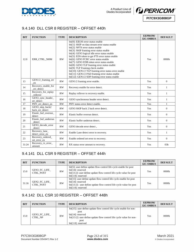
PI7C9X3G808GP Page 212 of 315 March 2021
Document Number DS43471 Rev 1-2 www.diodes.com © Diodes Incorporated
PI7C9X3G808GP
9.4.140 DLL CSR 8 REGISTER – OFFSET 440h
BIT FUNCTION TYPE DESCRIPTION EEPROM/
I2C-SMBUS DEFAULT
12:0 ERR_CTRL_500M RW
bit[0]: EIEOS error status enable
bit[1]: SKIP on data stream error status enable bit[2]: NFTS error status enable
bit[3]: SKIP framing error status enable
bit[4]: GEN3 logical idle error status enable bit[5]: EDS token to get FTS error status enable
bit[6]: GEN3 FCRC error status enable bit[7]: GEN3 EDB token error status enable
bit[8]: GEN3 TLP framing error status enable
bit[9]: TLP Framing check enable
bit[10]: GEN1/2 TLP framing error status error enable
bit[11]: GEN1/2 PAD framing error status enable bit[12]: GEN1/2 SDP framing error status enable
Yes 0000h
13 GEN1/2_framing_err
_en RW GEN1/2 framing error enable. Yes 0
14 Recovery_enable_for_err_detect
RW Recovery enable for error detect. Yes 1
15 Recovery_for_replay
_rollover RW Replay rollover to recovery enable. Yes 1
16 GEN3_sync_header_
err_detect RW GEN3 synchronous header error detect. Yes 1
17 PHY_err_detect_en RW PHY status error detect enable. Yes 1
18 GEN3_skip_back2 back_err_detect
RW GEN3 SKIP back 2 back error detect. Yes 0
19 Elastic_buf_overrun_
detect RW Elastic buffer overrun detect. Yes 0
20 Elastic_buf_underrun
_detect RW Elastic buffer underrun detect. Yes 0
21 GEN3_decode_error_detect
RW GEN3 decode error detect , Yes 0
22 Recovery_lane_
detect_error_en RW Enable Lane detect error to recovery. Yes 1
23 Recovery_ordered_
set_error_en RW Enable ordered set error to recovery. Yes 0
31:24 Recovery_rx_error_ amount
RW RX status error amount to recovery. Yes 03h
9.4.141 DLL CSR 9 REGISTER – OFFSET 444h
BIT FUNCTION TYPE DESCRIPTION EEPROM/
I2C-SMBUS DEFAULT
15:0 GEN3_FC_LIFE_ CTRL_POST
RW
bit[5]: user define update flow control life cycle enable for post
bit[14]: reserved bit[13:2]: user define update flow control life cycle value for post
bit[1:0]: reserved
Yes 0000h
31:16 GEN2_FC_LIFE_
CTRL_POST RW
bit[15]: user define update flow control life cycle enable for post bit[14]: reserved
bit[13:2]: user define update flow control life cycle value for post
bit[1:0]: reserved
Yes 0000h
9.4.142 DLL CSR 10 REGISTER – OFFSET 448h
BIT FUNCTION TYPE DESCRIPTION EEPROM/
I2C-SMBUS DEFAULT
15:0 GEN3_FC_LIFE_ CTRL_NP
RW
bit[15]: user define update flow control life cycle enable for non-
post
bit[14]: reserved bit[13:2]: user define update flow control life cycle value for non-
post bit[1:0]: reserved
Yes 0000h

PI7C9X3G808GP Page 213 of 315 March 2021
Document Number DS43471 Rev 1-2 www.diodes.com © Diodes Incorporated
PI7C9X3G808GP
BIT FUNCTION TYPE DESCRIPTION EEPROM/
I2C-SMBUS DEFAULT
31:16 GEN2_FC_LIFE_ CTRL_NP
RW
bit[15]: user define update flow control life cycle enable for non-post
bit[14]: reserved bit[13:2]: user define update flow control life cycle value for non-
post
bit[1:0]: reserved
Yes 0000h
9.4.143 DLL CSR 11 REGISTER – OFFSET 44Ch
BIT FUNCTION TYPE DESCRIPTION EEPROM/
I2C-SMBUS DEFAULT
15:0 GEN3_FC_LIFE_ CTRL_CPL
RW
bit[15]: user define update flow control life cycle enable for
completion
bit[14]: reserved bit[13:2]: user define update flow control life cycle value for
completion bit[1:0]: reserved
Yes 0000h
31:16 GEN2_FC_LIFE_
CTRL_CPL RW
bit[15]: user define update flow control life cycle enable for
completion bit[14]: reserved
bit[13:2]: user define update flow control life cycle value for
completion bit[1:0]: reserved
Yes 0000h
9.4.144 DLL CSR 12 REGISTER – OFFSET 450h
BIT FUNCTION TYPE DESCRIPTION EEPROM/
I2C-SMBUS DEFAULT
0 SKIP_LFSR_CTRL_
500M RW GEN3 LFSR value correct enable by SKIP. Yes 1
1 tlp_payload_ignore_
detect RW TLP payload ignore detect. Yes 0
2 x16_tlp_back2back_cal_en
RW For x16 TLP back 2 back calculate enable for receiver. Yes 0
3 Force_disable_tlp_
send RW Force to disable TLP sent when TLP empty. Yes 1
6:4 GEN3_de-
skew_reset_count RW GEN3 de-skew reset count. Yes 111b
7 GEN3_rx_eidle_en RW GEN3 Rx electric idle enable for data valid or not Yes 1
10:8 GEN1/2_de-skew_reset_count
RW GEN1/2 de-skew reset count. Yes 111b
27:11 Reserved RscdP Not support. No 0050h
31:28 x16_tlp_back2back_count
RO x16 TLP back 2 back count. Use bit 2 to clear. Yes 0h
9.4.145 DLL CSR 13 REGISTER – OFFSET 454h
BIT FUNCTION TYPE DESCRIPTION EEPROM/
I2C-SMBUS DEFAULT
0 NULLIFIED_FLAG
_500M RO Nullified TLP detect. No 0
1 ENDING_FLAG_
500M RO Ending of TLP is not consistent to total length. No 0
2 SEQ_NUM_ERR_ DET
RO Sequel number wrong. No 0
3 BUFFER_FULL_
DET RO Retry buffer is full. No 0
4 ECC_Correct RO ECC correctable detect error. No 0
5 ECC_Uncorrect RO ECC uncorrectable detect error. No 0
6 REPLAY__DET RO Replay timeout detect. No 0
7 CRC16_DET RO SDP of data link layer of CRC error detect. No 0
8 CRC32_DET RO TLP of data link layer of CRC error detect. No 0

PI7C9X3G808GP Page 214 of 315 March 2021
Document Number DS43471 Rev 1-2 www.diodes.com © Diodes Incorporated
PI7C9X3G808GP
BIT FUNCTION TYPE DESCRIPTION EEPROM/
I2C-SMBUS DEFAULT
9 CRC32_NULL_DET RO TLP of data link layer of nullified CRC detect. No 0
11:10 Reserved RsvdP Not support. No 00b
14:12 RX PM ACK
Number RW Used to set rx PM ACK number. The range is from 0 to 6. Yes 011b
15 Reserved RsvdP Not support. No 1
18:16 TX PM ACK
Number RW Used to send tx PM ACK number. The range is from 0 to 6. Yes 000b
31:19 Reserved RsvdP
Not support.
If the link is x16, the default value is 11E3h. Otherwise, the default value is 01E3h
No 03E3h
9.4.146 DLL CSR 14 REGISTER – OFFSET 458h
BIT FUNCTION TYPE DESCRIPTION EEPROM/
I2C-SMBUS DEFAULT
11:0 RX_NAK_SEQ_
NUM RO NAK sequence number record for receiver. Yes 000h
14:12 Reserved RsvdP Not support. No 000b
15 RX_NAK_FLAG RO NAK flag asserted of receiver. No 0
27:16 TX_NAK_SEQ_
NUM RO NAK sequence number record for transmitter. Yes 000h
30:28 Reserved RsvdP Not support. No 000b
31 TX_NAK_FLAG RO NAK flag asserted of transmitter. No 0
9.4.147 DLL CSR 15 REGISTER – OFFSET 45Ch
BIT FUNCTION TYPE DESCRIPTION EEPROM/
I2C-SMBUS DEFAULT
0 Nullified Enable RW When set, enable to generated nullified packet. Yes 1
1 Data Link Layer Reset
RW1C Reset of data link layer. Yes 0
2 TLP Ending Choice RW TLP of Ending choice by length or write to buffer. Yes 0
3 Block List Full
Select RW TLP Block list full select enable. Yes 0
7:4 RxReceive Threshold
Value RW Rx receive threshold value. Yes 8h
8 x16 Low Latency Enable
RW x16 low latency enable when common mode Yes 0
9 x16 Synchronous
Mode RW x16 Tx synchronous enable when common mode. Yes 0
12:10 GEN1_FTS_skew_
Range_value RW GEN1 FTS skew range value. Yes 011b
15:13 GEN2_FTS_skew_ Range_value
RW GEN2 FTS skew range value. Yes 001b
19:16 GEN1_de-skew_
range_value RW GEN1 de-skew range value. Yes Ch
23:20 GEN2_de-skew_ range_value
RW GEN2 de-skew range value. Yes Ch
27:24 GEN3_de-skew_ Rnage_value
RW GEN3 de-skew range value. Yes Ch
28
L0 State and Non
valid for Surprise Disconnect
RW Internal used only. Yes 0
29 Port Bifurcating
Enable RW When set, enable port bifurcating function. Yes 0
30 Skip_mask_select_en RW SKIP mask select enable for DLP. Yes 0
31 Reserved RsvdP Not support. No 0

PI7C9X3G808GP Page 215 of 315 March 2021
Document Number DS43471 Rev 1-2 www.diodes.com © Diodes Incorporated
PI7C9X3G808GP
9.4.148 DLL CSR 16 REGISTER – OFFSET 460h
BIT FUNCTION TYPE DESCRIPTION EEPROM/
I2C-SMBUS DEFAULT
31:0 DLL_TX_DEBUG_i RO Internal used only. No 0000_0070h
9.4.149 DLL CSR 17 REGISTER – OFFSET 464h
BIT FUNCTION TYPE DESCRIPTION EEPROM/
I2C-SMBUS DEFAULT
31:0 DLL_RX_DEBUG_i RO Internal used only. No 0000_0000h
9.4.150 DLL CSR 18 REGISTER – OFFSET 468h
BIT FUNCTION TYPE DESCRIPTION EEPROM/
I2C-SMBUS DEFAULT
31:0 MAC_TX_DEBUG_i
RO Internal used only. No 0098_0029h
9.4.151 DLL CSR 19 REGISTER – OFFSET 46Ch
BIT FUNCTION TYPE DESCRIPTION EEPROM/
I2C-SMBUS DEFAULT
31:0 MAC_RX_DEBUG_
i RO Internal used only. No 0000_0000h
9.4.152 LA DEBUG REGISTER – OFFSET 470h
BIT FUNCTION TYPE DESCRIPTION EEPROM/
I2C-SMBUS DEFAULT
3:0 initial flow control 2 RW Internal used only. Yes 1011b
4 flow control life
cycle synchronous RW Internal used only. Yes 0
5 initial flow control 2 expire enable
RW Internal used only. Yes 0
6 GEN3 auto change
lane width RW Internal used only. Yes 1
7 de-skew delay time disable
RW Internal used only. Yes 1
31:8 misc RW Internal used only. Yes 0000_00h
9.4.153 TL CSR 0 REGISTER – OFFSET 4C0h
BIT FUNCTION TYPE DESCRIPTION EEPROM/
I2C-SMBUS DEFAULT
0 decode_vga RW 0b: disable VGA decode 1b: enable VGA decode
Yes 1
1 msi_cap_dis RO 0b: enable MSI capability
1b: disable MSI capability Yes 0
2 pwr_cap_dis RO 0b: enable power capability
1b: disable power capability Yes 0
3 mf_credit_update_ dis
RO Internal used only. Yes 0
4 mc_cap_dis RO Internal used only. Yes 0
5 mem_sharing_dis RO
0b: enable memory sharing
1b: disable memory sharing
It is set by Port 0 only. When set, it will affect the entire switch.
Yes 0
7:6 Reserved RsvdP Not support. No 00b
8 p_inta_slot RW Internal used only. Yes 0
9 p_inta_gpio RW Internal used only. Yes 0

PI7C9X3G808GP Page 216 of 315 March 2021
Document Number DS43471 Rev 1-2 www.diodes.com © Diodes Incorporated
PI7C9X3G808GP
BIT FUNCTION TYPE DESCRIPTION EEPROM/
I2C-SMBUS DEFAULT
10 p_inta_ntl RW Internal used only. Yes 0
11 Reserved RsvdP Not support. No 0
13:12 initial credit
threshold RO Internal used only. Yes 00b
31:14 Reserved RsvdP Not support. No 0-0h
9.4.154 TL CSR 1 REGISTER – OFFSET 4C4h
BIT FUNCTION TYPE DESCRIPTION EEPROM/
I2C-SMBUS DEFAULT
0 store_en RW
When set, a store-forward mode is used. Otherwise, the chip is
working under cut-through mode.
It is valid for upstream port only.
Yes 0
3:1 cut-through threshold RW
Cut-through Threshold.
00b: the threshold is set at the middle of forwarding packet
01b: the threshold is set ahead 1-cycle of middle point 10b: the threshold is set ahead 2-cycle of middle point
11b: the threshold is set ahead 3-cycle of middle point
It is valid for upstream port only.
Yes 100b
4 port_arb_mode RW
When set, the round-robin arbitration will stay in the arbitrated port even if the credit is not enough but request is pending.
When clear, the round-robin arbitration will always go to the
requesting port, which the outgoing credit is enough for the packet queued in the port.
It is valid for upstream port only
Yes 0
5 port_order RW
When set, there is forced ordering rule on packets for different
egress port.
It is valid for upstream port only.
Yes 0
6 cpl_order RW
When set, there is forced ordering rule between completion packet with different tag.
It is valid for upstream port only.
Yes 0
7 np_store_en RW
When set, for Non-post TLP store-forward mode is used.
Otherwise, Non-post TLP is working under cut-through mode.
It is valid for upstream port only.
Yes 0
8 Reserved RW Internal used only. No 0
9 datasel_rw_en RO When set, PM data register’s DATA SEL is R/W. Yes 0
10 Reserved RW Internal used only. No 0
11 4k_boundary_check_
en RW
0b: disable
1b: enable 4KB boundary check Yes 0
12 Reserved RsvdP Not support. No 0
13 order_rule5_en RW When set, Post packet cannot pass Non-post Packet.
Yes 0
14 ordering_forzen_p_ dis
RW For Post packets. Yes 0
15 ordering_forzen_np_
dis RW For Non-Post packets. Yes 1
16 RX Poison TLP
mode RW Internal used only. Yes 0
17 RX ECRC TLP mode
RW Internal used only. Yes 0
18 RX MC overlay TLP
ECRC mode RW Internal used only. Yes 0
31:19 Reserved RsvdP Not support. No 0-0h

PI7C9X3G808GP Page 217 of 315 March 2021
Document Number DS43471 Rev 1-2 www.diodes.com © Diodes Incorporated
PI7C9X3G808GP
9.4.155 TL CSR 2 REGISTER – OFFSET 4C8h
BIT FUNCTION TYPE DESCRIPTION EEPROM/
I2C-SMBUS DEFAULT
0 dma_cap RO When Set, DMA is enabled. Yes 0
1 non_trans_ RO When Set, non transparent mode is enabled. Yes 1
2 Power_saving_en RO When set power saving mode is enabled.
It is set by Port 0 only. When set, it will affect the entire switch.
Yes 1
3 Reserved RW Not support. No 0
4 overlay_tlp_fc_ update_mode
RW When set, overlay tlp fc update mode is set.
Yes 1
5 egress_tlp_request _
mode RW
When set, egress tlp request mode is set.
It is set by Port 0 only. When set, it will affect the entire switch.
Yes 0
7:6 Reserved RW Internal used only. Yes 0
31:7 Reserved RsvdP Not support. No 0_0h
9.4.156 TL CSR 3 REGISTER – OFFSET 4CCh (Port 0 Only)
BIT FUNCTION TYPE DESCRIPTION EEPROM/
I2C-SMBUS DEFAULT
3:0 vp port ring_csr RO Internal used only. Yes 1010b
4 vp port cut through
ctrl RO Internal used only. Yes 0
31:5 Reserved RsvdP Not support. No 0_0h
9.4.157 TL CSR 4 REGISTER – OFFSET 4D0h
BIT FUNCTION TYPE DESCRIPTION EEPROM/
I2C-SMBUS DEFAULT
23:0 Reserved RsvdP Not support. No 00_0000h
31:24 specific TL debug
mode_sel RW Internal used only. Yes 00h
9.4.158 DEVICE CONFIGURATION 0 REGISTER – OFFSET 504h (Port 0 Only)
BIT FUNCTION TYPE DESCRIPTION
EEPROM/
I2C-
SMBUS
DEFAULT
2:0 Up Port Selection RO
Used to do up port selection.
It is valid for transparent mode only.
Yes 000b
5:3 Reserved RsvdP Not support. No 000b
6 Chip CD Mode RO
Used to enable CD mode for the whole chip.
1: Enable Chip CD mode (i.e. switch operates in cross-domain mode)
0: Disable Chip CD mode (i.e. switch operates in transparent mode)
Yes 0
7 Smbus Enable RO
Used to set SMBUS_EN_L strap pin.
0b: I2C 1b: SMBUS
Yes 0
10:8 I2C/Smbus Address RO Used to set I2C_ADDRESS[2:0] strap pins. Yes
Set by
I2C_ADDRESS [2:0]
11 Debug_Mode RO 0b: disable debug mode
1b: enable debug mode Yes 0
31:12 Reserved RsvdP Not support. No 0000_0h

PI7C9X3G808GP Page 218 of 315 March 2021
Document Number DS43471 Rev 1-2 www.diodes.com © Diodes Incorporated
PI7C9X3G808GP
9.4.159 DEVICE CONFIGURATION 1 REGISTER – OFFSET 508h (Port 0 Only)
BIT FUNCTION TYPE DESCRIPTION EEPROM/
I2C-SMBUS DEFAULT
1:0 Reserved RsvdP Not support. No 00b
4:2 PORTCFG RO Used to set PORTCFG[2:0] strap pins. Yes
Set by
PORTCFG [2:0]
6:5 Chip Mode RO Used to set CHIPMODE [1:0] strap pins. Yes 00b
7 Fast Mode RO 0b: disable fast mode 1b: enable fast mode, for internal used only
Yes 0
8 Ckmode RO Used to set CKMODE strap pin. Yes 0
31:9 Reserved RsvdP Not support. No 0-0b
9.4.160 DEVICE CONFIGURATION 2 REGISTER – OFFSET 50Ch (Port 0 Only)
BIT FUNCTION TYPE DESCRIPTION EEPROM/
I2C-SMBUS DEFAULT
0 Reserved RsvdP Not support. No 0
1 HotPlug_Enable RO
Used to set HOT_PLUG_EN_L strap pin.
0b: disable 1b: enable
Yes 1
2 Surprise_Hot_Plug_Disable
RO
Used to set SURPRISE_HP strap pin.
0b: enable
1b: disable
Yes 0
3 IOE_40Bit_Disable RO
Used to set IOE is 16 bit or 40 bit.
0b: 40 bit IOE 1b: 16 bit IOE
Yes 0
4 Pm_L1_1_Enable RO
Used to set PM_L11_EN_L strap pin.
0b: disable
1b: ensable
Yes Set by
PM_L11_EN
_L
7:5 Rserved RsvdP Not support. No 001b
8 CLKBUF_PD RO Used to set CLKBUFPD_L strap pin. Yes 1
14:9 Reserved RsvdP Not support. No 000000b
15 P4_RID_Auto_Set RO Used to set RID table being automatically built and maintained by
the switch hardware in CDLEP Port 4. Yes 1b
17:16 Switch CD Mode RO
Used to configure CDEP Port for this switch.
0xb: no CDEP ports configured in this switch 10b: not support
11b: one CDVEP port and one CDLEP port
The setting in Switch CD Mode can be ignored if Chip CD Mode is
disabled.
Yes 00b
19:18 DMA Mode RO
Used to configure DMA Mode for this switch.
0xb: DMA functions are disabled in this switch 10b: DMA function s enabled under its own main or local hosts
Switch CD Mode = 0x: DMA functions are at P0 only Switch CD Mode = 11: DMA functions are at P0 and P4
respectively
11b: DMA function only enabled under the main host domain and DMA functions are enabled at P0 only
Yes 00b
20 CLKBUF_CTL_EN RO Used to enable internal clock buffer outputs control. Yes 0
21 Reserved RsvdP Not support. No 0
22 Reserved RsvdP Not support. No 0
23 Reserved RsvdP Not support. No 0

PI7C9X3G808GP Page 219 of 315 March 2021
Document Number DS43471 Rev 1-2 www.diodes.com © Diodes Incorporated
PI7C9X3G808GP
BIT FUNCTION TYPE DESCRIPTION EEPROM/
I2C-SMBUS DEFAULT
31:24 CLKBUF_Output_
En RO
Used to enable/disable internal clock buffer outputs REFCLKOP/N[7:0]
0b: disable
1b: enable
These bits are valid when bit[20]=1.
Yes FFh
9.4.161 DEVICE CLOCK EXTERNAL CONTROL REGISTER – OFFSET 510h (Port 0 Only)
BIT FUNCTION TYPE DESCRIPTION EEPROM/
I2C-SMBUS DEFAULT
15:0 EE_Ext_Pclk_Req RO Device Ext_Pclk_Req Control from EEPROM. Yes/No 0000h
19:16 EE_Mplla_Force_En RO Device Mplla_Force_En able Control from EEPROM. Yes/No 0h
23:20 EE_Ref_Use_Pad RO Device Ref_Use_Pad _Enable Control from EEPROM. Yes/No 0h
27:24 EE_Ref_Repeat_Clk
_En RO Device Ref_Repeat_Clk_Enable Control from EEPROM. Yes/No 0h
28 EE_Phy_Control_En RO Device Phy Clock External Control Enable from EEPROM. Yes/No 0
29 Valid for bit[19:16] RO 1b: bit[19:16] are valid. Yes/No 0
30 Valid for bit[23:20] RO 1b: bit[23:20] are valid. Yes/No 0
31 Reserved RsvdP Not support. No 0
9.4.162 DEVICE SRIS EXTERNAL CONTROl REGISTER – OFFSET 514h (Port 0 Only)
BIT FUNCTION TYPE DESCRIPTION EEPROM/
I2C-SMBUS DEFAULT
0 lane 0_Sris_Mode RO Lane 0_Sris_ModeExternal Control from EEPROM. Yes/No 0
1 lane 1_Sris_Mode RO Lane 1_Sris_ModeExternal Control from EEPROM. Yes/No 0
2 lane 2_Sris_Mode RO Lane 2_Sris_ModeExternal Control from EEPROM. Yes/No 0
3 lane 3_Sris_Mode RO Lane 3_Sris_ModeExternal Control from EEPROM. Yes/No 0
7:4 Reserved RsvdP Not support. No 0h
8 lane 4_Sris_Mode RO Lane 4_Sris_ModeExternal Control from EEPROM. Yes/No 0
9 lane 5_Sris_Mode RO Lane 5_Sris_ModeExternal Control from EEPROM. Yes/No 0
10 lane 6_Sris_Mode RO Lane 6_Sris_ModeExternal Control from EEPROM. Yes/No 0
11 lane 7_Sris_Mode RO Lane 7_Sris_ModeExternal Control from EEPROM. Yes/No 0
30:12 Reserved RsvdP Not support. No 0-0b
31 Sris External Control
En RO Device Sris External Control Enble. Yes/No 0
9.4.163 DEVICE COMM REFCLK MODE EXTERNAL CONTOL REGISTER – OFFSET 518h (Port 0 Only)
BIT FUNCTION TYPE DESCRIPTION EEPROM/
I2C-SMBUS DEFAULT
0 lane 0_Cmn_Refclk_ Mode
RO Lane 0_Cmm Refclk ModeExternal Control from EEPROM. Yes/No 0
1 lane 1_Cmn_Refclk_
Mode RO Lane 1_Cmm Refclk ModeExternal Control from EEPROM. Yes/No 0
2 lane 2_Cmn_Refclk_ Mode
RO Lane 2_Cmm Refclk ModeExternal Control from EEPROM. Yes/No 0
3 lane 3_Cmn_Refclk_
Mode RO Lane 3_Cmm Refclk ModeExternal Control from EEPROM. Yes/No 0
7:4 Reserved RsvdP Not support. No 0h
8 lane 4_Cmn_Refclk_
Mode RO Lane 4_ Cmm Refclk ModeExternal Control from EEPROM. Yes/No 0
9 lane 5_Cmn_Refclk_
Mode RO Lane 5_ Cmm Refclk ModeExternal Control from EEPROM. Yes/No 0
10 lane 6_Cmn_Refclk_ Mode
RO Lane 6_ Cmm Refclk ModeExternal Control from EEPROM. Yes/No 0

PI7C9X3G808GP Page 220 of 315 March 2021
Document Number DS43471 Rev 1-2 www.diodes.com © Diodes Incorporated
PI7C9X3G808GP
BIT FUNCTION TYPE DESCRIPTION EEPROM/
I2C-SMBUS DEFAULT
11 lane 7_Cmn_Refclk_ Mode
RO Lane 7_ Cmm Refclk ModeExternal Control from EEPROM. Yes/No 0
30:12 Rserved RsvdP Not support. No 0-0b
31 Cmn_Refclk_Mode External Control En
RO Device Cmm Refclk Mode External Control Enble. Yes/No 0
9.4.164 MBIST CFG CONTROL REGISTEr – OFFSET 51Ch (Port 0 Only)
BIT FUNCTION TYPE DESCRIPTION EEPROM/
I2C-SMBUS DEFAULT
0 Cfg_Mbist_En RW Used to set Mbist Enable from CFG Control. Yes 0000h
1 Cfg_Mbist_mode RW Used to set Mbist En from Pin or CFG. Yes 0h
31:2 Cfg_Mbist_done RO Used to indicate Mbist test Done. No 0-0h
9.4.165 MBIST CFG STATUS REGISTER – OFFSET 520h (Port 0 Only)
BIT FUNCTION TYPE DESCRIPTION EEPROM/
I2C-SMBUS DEFAULT
29:0 Cfg_Mbist_Error RO
Used to indicate Mbist error.
It can be read from I2C-SMBUS only.
No 0-0h
31:30 Reserved RsvdP Not support. No 00b
9.4.166 NOC BIST CONTROL REGISTER – OFFSET 524h (Port 0 Only)
BIT FUNCTION TYPE DESCRIPTION EEPROM/
I2C-SMBUS DEFAULT
0 Noc Bist Enable RO Used to enable Noc Bist Test. Yes/No 0
1 Noc_Bist_Enable_sel RO
Used to select the NOC Bist Enable Source.
1b: Noc Bist Control Register bit[0]
0b: Jtag
Yes/No 0
23:2 Reserved RsvdP Not support. No 0-0b
31:24 Noc Bist Status RO
Noc Bist Status.
It can be read from I2C-SMBUS only.
No 00h
9.4.167 EXTERNAL LOOPBACK PRBS CONTOL REGISTER – OFFSET 528h (Port 0 Only)
BIT FUNCTION TYPE DESCRIPTION EEPROM/
I2C-SMBUS DEFAULT
1:0 Lane 3-0 PRBS Rate RW
Choose Lane 3-0 PRBS Rate.
00b: GEN1
01b: GEN2 10b: GEN3
11b: Reserved
Yes 00b
3:2 Reserved RsvdP Not support. No 00b
5:4 Lane 7-4 PRBS Rate RW
Choose Lane 7-4 PRBS Rate.
00b: GEN1 01b: GEN2
10b: GEN3
11b: Reserved
Yes 00b
7:6 Reserved RsvdP Not support. No 00b

PI7C9X3G808GP Page 221 of 315 March 2021
Document Number DS43471 Rev 1-2 www.diodes.com © Diodes Incorporated
PI7C9X3G808GP
BIT FUNCTION TYPE DESCRIPTION EEPROM/
I2C-SMBUS DEFAULT
8 Lane 3-0 PRBS Rate Enable
RW
When enabled, Lane 3-0 is set to PRBS rate as indicated in bit[1:0] to run loopback test.
Please note an external test fixture must be provided to loopback
TX to RX. Also, please follow PRBS Appnote to set TXEQ
PRESET value at GEN3 speed through CR interface.
Yes 0
9 Reserved RsvdP Not support. No 0
10 Lane 7-4 PRBS
Rate Enable RW
When enabled, Lane 7-4 is set to PRBS rate as indicated in bit[5:4]
to run loopback test.
Please note an external test fixture must be provided to loopback TX to RX. Also, please follow PRBS Appnote to set TXEQ
PRESET value at GEN3 speed through CR interface.
Yes 0
31:11 Reserved RsvdP Not support. No 0000_0h
9.4.168 PHY SRAM PROGRAM 0 REGISTER – OFFSET 52Ch (Port 0 Only)
BIT FUNCTION TYPE DESCRIPTION EEPROM/
I2C-SMBUS DEFAULT
15:0 PHY SRAM DATA RO PHY SRAM DATA. Yes/No 0000h
31:16 PHY SRAM
OFFSET RO PHY SRAM OFFSET. Yes/No 0000h
9.4.169 PHY SRAM PROGRAM 1 REGISTER – OFFSET 530h (Port 0 Only)
BIT FUNCTION TYPE DESCRIPTION EEPROM/
I2C-SMBUS DEFAULT
0 PHY SRAM Program Enable
RO Start PHY SRAM Program. Yes/No 0
1 PHY SRAM
Program Done RO Finish PHY SRAM Program. Yes/No 0
31:17 Reserved RsvdP Not support. No 0-0h
9.4.170 FAILOVER CONTROL REGISTER – OFFSET 534h (Port 0 Only)
BIT FUNCTION TYPE DESCRIPTION EEPROM/
I2C-SMBUS DEFAULT
0 Reserved RsvdP Not support. 0
1 dis_dn_hotreset RW
Used to disable up link down, fire down port hot-reset event.
0b: enable
1b: disable
Yes 0
2 En_up_keep_enum RW
Used to enable up link down, keep up port enum data.
0b: disable 1b: enable
Yes 0
31:3 Reserved ResvP Not support. No 0-0b
9.4.171 THERMAL SENSOR INT MASK AND STATUS REGISTER – OFFSET 538h (Port 0 Only)
BIT FUNCTION TYPE DESCRIPTION EEPROM/
I2C-SMBUS DEFAULT
2:0 thermal sensor 2~0 status
RW1C Thermal sensor 2~0 status. Yes 000b
15:3 Reserved RsvdP Not support. No 0-0b
18:16 thermal sersor 2~0
interrupt mask RW Thermal sersor 2~0 interrupt mask. Yes 111b
31:19 Reserved RsvdP Not support. No 0-0b
31:7 Reserved RsvdP Not support. No 0-0h

PI7C9X3G808GP Page 222 of 315 March 2021
Document Number DS43471 Rev 1-2 www.diodes.com © Diodes Incorporated
PI7C9X3G808GP
9.4.172 THERMAL SENSOR CONTROL REGISTER – OFFSET 53Ch (Port 0 Only)
BIT FUNCTION TYPE DESCRIPTION EEPROM/
I2C-SMBUS DEFAULT
0 Thermal Sensor 0
Status RO Used to indicate the temp over the Threshold No 0b
1 Thermal Sensor 1 Status
RO Used to indicate the temp over the Threshold No 0b
2 Thermal Sensor 2
Status RO Used to indicate the temp over the Threshold No 0b
23:3 Reserved RsvdP Not support. No 0_0h
25:24 Thermal Sensor 0
Threshold RW
Used to set the threshold of chip temperature.
00b:110
01b:120
10b: 130 11b: 140
Yes 0
27:26 Thermal Sensor 1
Threshold RW
Used to set the threshold of chip temperature.
00b:110
01b:120 10b: 130
11b: 140
Yes 0
29:28 Thermal Sensor 2
Threshold RW
Used to set the threshold of chip temperature.
00b:110
01b:120 10b: 130
11b: 140
Yes 0
30 Reserved RsvdP Not support. No 0
31 Auto Test Temp. RW Used to set Thermal Sensor burst test Enable Yes 0
9.4.173 DEVICE ELASTIC BUFFER EMPTY MODE EXTERNAL CONTROL REGISTER – OFFSET 540h (Port 0 Only)
BIT FUNCTION TYPE DESCRIPTION EEPROM/
I2C-SMBUS DEFAULT
0 lane 0_Eb_Empty_
Mode RO Lane 0_ Eb_Empty_Mode External Control from EEPROM. Yes/No 0
1 lane 1_Eb_Empty_
Mode RO Lane 1_ Eb_Empty_Mode External Control from EEPROM. Yes/No 0
2 lane 2_Eb_Empty_ Mode
RO Lane 2_ Eb_Empty_Mode External Control from EEPROM. Yes/No 0
3 lane 3_Eb_Empty_
Mode RO Lane 3_ Eb_Empty_Mode External Control from EEPROM. Yes/No 0
7:4 Reserved RsvdP Not support. No 0h
8 lane 4_Eb_Empty_
Mode RO Lane 4_ Eb_Empty_Mode External Control from EEPROM. Yes/No 0
9 lane 5_Eb_Empty_ Mode
RO Lane 5_ Eb_Empty_Mode External Control from EEPROM. Yes/No 0
10 lane 6_Eb_Empty_
Mode RO Lane 6_ Eb_Empty_Mode External Control from EEPROM. Yes/No 0
11 lane 7_Eb_Empty_
Mode RO Lane 7_ Eb_Empty_Mode External Control from EEPROM. Yes/No 0
30:12 Rserved RsvdP Not support. No 0-0b
31 Eb_Empty_Mode External Control En
RO Device Cmm Refclk Mode External Control Enble. Yes/No 0
9.4.174 DEVICE MISC REGISTER – OFFSET 544h (Port 0 Only)
BIT FUNCTION TYPE DESCRIPTION EEPROM/
I2C-SMBUS DEFAULT
0 HW_Init_Load RO When set, it means eeprom preloading is done. Yes/No 0
31:1 Rserved RsvdP Not support. No 0-0b

PI7C9X3G808GP Page 223 of 315 March 2021
Document Number DS43471 Rev 1-2 www.diodes.com © Diodes Incorporated
PI7C9X3G808GP
9.4.175 SWITCH DOMAIN MODE CONTROL – OFFSET 558h (Port 0 Only)
BIT FUNCTION TYPE DESCRIPTION EEPROM/
I2C-SMBUS DEFAULT
7:0 Reserved RsvdP Not support. No 00h
13:8 Broadcast idx RW Used to enable destination switch for broadcast message. Yes 00_0001b
31:14 Reserved RsvdP Not support. No 0-0h
9.4.176 PORT CLOCK CONTROL REGISTER – OFFSET 55Ch (Port 0 Only)
BIT FUNCTION TYPE DESCRIPTION EEPROM/
I2C-SMBUS DEFAULT
15:8 Rserved RsvdP Not support. No 0000h
16 Port Clock control
Enable RW Used to enable Port Clock control function. Yes 0
23:17 Rserved RsvdP Not support. No 0-0h
31:24 Port Clock Enable RW
Used to set Port Clock Enable.
0b: disable
1b: enable
These bits are valid when bit[16]=1.
Yes FFh
9.4.177 PERFORMANCE COUNTER CONTROL REGISTER – OFFSET 56Ch
BIT FUNCTION TYPE DESCRIPTION EEPROM/
I2C-SMBUS DEFAULT
0 counter_start_stop RW 1b: Performance counter start counting
0b: Performace counter stop counting Yes 0
1 counter_clear WO
1b: clear performace counter.
It is valid when bit[4]=1 and is always read as 0b.
Yes 0
3:2 Reserved RsvdP Not support. No 00b
4 counter_enable RW 1b: Performance counter is controlled by s/w (bit[0])
0b: Performance counter is controlled by h/w (autorun) No 0
31:5 Reserved RsvdP Not support. No 0-0h
9.4.178 PHY SOURCE SELECT REGISTER – OFFSET 570h
BIT FUNCTION TYPE DESCRIPTION EEPROM/
I2C-SMBUS DEFAULT
7:0 Lanexx phy_source
select RW Internal used only. Yes 00h
8 Valid for bit[7:1] RW 1b: bit[7:0] are valid. Yes 0
31:9 Reserved RsvdP Not support. No 0-0h
9.4.179 NIC CTRL 0 REGISTER – OFFSET 5A0h (Port 0 Only)
BIT FUNCTION TYPE DESCRIPTION EEPROM/
I2C-SMBUS DEFAULT
7:0 Debug Select RW Select Debug Nic Signal. Yes 00h
9:8 Cmd Arbiter Delay RW Delay cycles for next cmd arbiter start. Yes 00b
15:10 Reserved RW Internal used only. Yes 0000_00b
16 Destination Credit
Wait RW
Wait until destination credit is enough to transmit packet.
0b: OFF 1b: ON
Yes 0
17 Reserved RsvdP Not support. No 0
20:18 Time Based RR
Time Period RW Time Period Selection for Time based Round Robin. Yes 000b
23:21 Reserved RW Internal used only. No 000b
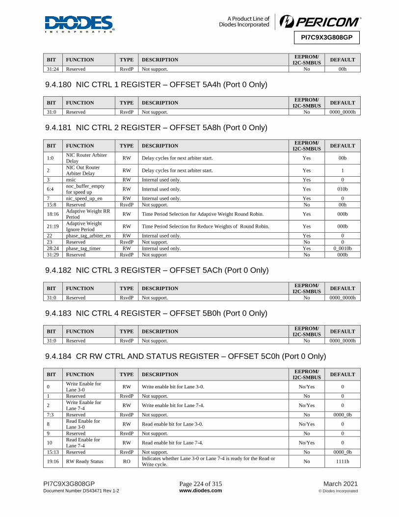
PI7C9X3G808GP Page 224 of 315 March 2021
Document Number DS43471 Rev 1-2 www.diodes.com © Diodes Incorporated
PI7C9X3G808GP
BIT FUNCTION TYPE DESCRIPTION EEPROM/
I2C-SMBUS DEFAULT
31:24 Reserved RsvdP Not support. No 00h
9.4.180 NIC CTRL 1 REGISTER – OFFSET 5A4h (Port 0 Only)
BIT FUNCTION TYPE DESCRIPTION EEPROM/
I2C-SMBUS DEFAULT
31:0 Reserved RsvdP Not support. No 0000_0000h
9.4.181 NIC CTRL 2 REGISTER – OFFSET 5A8h (Port 0 Only)
BIT FUNCTION TYPE DESCRIPTION EEPROM/
I2C-SMBUS DEFAULT
1:0 NIC Router Arbiter
Delay RW Delay cycles for next arbiter start. Yes 00b
2 NIC Out Router Arbiter Delay
RW Delay cycles for next arbiter start. Yes 1
3 msic RW Internal used only. Yes 0
6:4 noc_buffer_empty for speed up
RW Internal used only. Yes 010b
7 nic_speed_up_en RW Internal used only. Yes 0
15:8 Reserved RsvdP Not support. No 00h
18:16 Adaptive Weight RR Period
RW Time Period Selection for Adaptive Weight Round Robin. Yes 000b
21:19 Adaptive Weight
Ignore Period RW Time Period Selection for Reduce Weights of Round Robin. Yes 000b
22 phase_tag_arbiter_en RW Internal used only. Yes 0
23 Reserved RsvdP Not support. No 0
28:24 phase_tag_timer RW Internal used only. Yes 0_0010b
31:29 Reserved RsvdP Not support No 000b
9.4.182 NIC CTRL 3 REGISTER – OFFSET 5ACh (Port 0 Only)
BIT FUNCTION TYPE DESCRIPTION EEPROM/
I2C-SMBUS DEFAULT
31:0 Reserved RsvdP Not support. No 0000_0000h
9.4.183 NIC CTRL 4 REGISTER – OFFSET 5B0h (Port 0 Only)
BIT FUNCTION TYPE DESCRIPTION EEPROM/
I2C-SMBUS DEFAULT
31:0 Reserved RsvdP Not support. No 0000_0000h
9.4.184 CR RW CTRL AND STATUS REGISTER – OFFSET 5C0h (Port 0 Only)
BIT FUNCTION TYPE DESCRIPTION EEPROM/
I2C-SMBUS DEFAULT
0 Write Enable for
Lane 3-0 RW Write enable bit for Lane 3-0. No/Yes 0
1 Reserved RsvdP Not support. No 0
2 Write Enable for
Lane 7-4 RW Write enable bit for Lane 7-4. No/Yes 0
7:3 Reserved RsvdP Not support. No 0000_0b
8 Read Enable for
Lane 3-0 RW Read enable bit for Lane 3-0. No/Yes 0
9 Reserved RsvdP Not support. No 0
10 Read Enable for
Lane 7-4 RW Read enable bit for Lane 7-4. No/Yes 0
15:13 Reserved RsvdP Not support. No 0000_0b
19:16 RW Ready Status RO Indicates whether Lane 3-0 or Lane 7-4 is ready for the Read or Write cycle.
No 1111h

PI7C9X3G808GP Page 225 of 315 March 2021
Document Number DS43471 Rev 1-2 www.diodes.com © Diodes Incorporated
PI7C9X3G808GP
BIT FUNCTION TYPE DESCRIPTION EEPROM/
I2C-SMBUS DEFAULT
31:20 Reserved RsvdP Not support. No 000h
9.4.185 CR CTRL 0 REGISTER – OFFSET 5C4h (Port 0 Only)
BIT FUNCTION TYPE DESCRIPTION EEPROM/
I2C-SMBUS DEFAULT
15:0 Lane 3-0 Data RW Contains the Lane 3-0 register data. Yes 0000h
31:16 Lane 3-0 Register RW Contains the Lane 3-0 register address. Yes 0000h
9.4.186 CR CTRL 1 REGISTER – OFFSET 5C8h (Port 0 Only)
BIT FUNCTION TYPE DESCRIPTION EEPROM/
I2C-SMBUS DEFAULT
31:0 Reserved RsvdP Not support. No 0000_0000h
9.4.187 CR CTRL 2 REGISTER – OFFSET 5CCh (Port 0 Only)
BIT FUNCTION TYPE DESCRIPTION EEPROM/
I2C-SMBUS DEFAULT
15:0 Lane 7-4 Data RW Contains the Lane 7-4 register data. Yes 0000h
31:16 Lane 7-4 Register RW Contains the Lane 7-4 register address. Yes 0000h
9.4.188 CR CTRL 3 REGISTER – OFFSET 5D0h (Port 0 Only)
BIT FUNCTION TYPE DESCRIPTION EEPROM/
I2C-SMBUS DEFAULT
31:0 Reserved RsvdP Not support. No 0000_0000h
9.4.189 THERMAL SENSOR TEST REGISTER – OFFSET 5D4h (Port 0 Only)
BIT FUNCTION TYPE DESCRIPTION EEPROM/
I2C-SMBUS DEFAULT
3:0 Thermal Sensor Test
Access Control RW Select Thermal Sensor Test Items. Yes 0h
5:4 Thermal Sensor Chip Select
RW
Chip Select for Thermal Sensor Test.
00b: Thermal Sensor 0 01b: Thermal Sensor 1
10b: Thermal Sensor 2 11b: Reserved
Yes 00b
6 Software Digital Test Mode
RW
Digital Test Enable.
0b: Disable
1b: Enable
Yes 0
7 Reserved RsvdP Not support. No 0
8 Digital Test Status RO
Indicate Success or Fail Status of Digital Test.
0b: Fail 1b: Success
No 0
9 Digital Test Mode 8 Status
RO
Indicate Success or Fail Status of Digital Test Mode 8.
0b: Fail
1b: Success
No 0
10 Digital Test Mode 9
Status RO
Indicate Success or Fail Status of Digital Test Mode 9.
0b: Fail
1b: Success
No 0
14:11 Reserved RsvdP Not support. No 0h

PI7C9X3G808GP Page 226 of 315 March 2021
Document Number DS43471 Rev 1-2 www.diodes.com © Diodes Incorporated
PI7C9X3G808GP
BIT FUNCTION TYPE DESCRIPTION EEPROM/
I2C-SMBUS DEFAULT
15 Digital Test Done RO
Thermal Sensor Digital Test Done Status.
0b: Test no complete 1b: Test complete
No 0
16 EEPROM Single
Read RW Internal used only. No 0
31:17 Reserved RsvdP Not support. No 0000h
9.4.190 THERMAL SENSOR CTRL 0 REGISTER – OFFSET 5D8h (Port 0 Only)
BIT FUNCTION TYPE DESCRIPTION EEPROM/
I2C-SMBUS DEFAULT
0 Thermal Sensor Burst Run
RW
Get Thermal Result periodically.
0b: OFF
1b: ON
Yes 0
1 Thermal Sensor
Single Run RW
Get Thermal Result Once.
0b: OFF
1b: ON
Yes 0
2 Thermal Sensor
Power Down RW
Trun off Thermal Sensor.
0b: disable power down 1b: enable power down
Yes 0
7:3 Reserved RsvdP Not support. No 0_0b
19:8 Thermal Sensor Conversion Data
Output
RO Thermal Sensor Results. No 000h
22:20 Reserved RsvdP Not support. No 000b
23 Thermal Sensor
Conversion Done RO
Get Thermal Sensor Result Done.
0b: Conversion not complete 1b: Conversion complete
No 0
31:24 Reserved RsvdP Not support. No 00h
9.4.191 THERMAL SENSOR CTRL 1 REGISTER – OFFSET 5DCh (Port 0 Only)
BIT FUNCTION TYPE DESCRIPTION EEPROM/
I2C-SMBUS DEFAULT
0 Thermal Sensor
Burst Run RW
Get Thermal Result periodically.
0b: OFF
1b: ON
Yes 0
1 Thermal Sensor
Single Run RW
Get Thermal Result Once.
0b: OFF 1b: ON
Yes 0
2 Thermal Sensor Power Down
RW
Trun off Thermal Sensor.
0b: disable power down
1b: enable power down
Yes 0
7:3 Reserved RsvdP Not support. No 0_0b
19:8
Thermal Sensor
Conversion Data
Output
RO Thermal Sensor Result. No 000h
22:20 Reserved RsvdP Not support. No 000b
23 Thermal Sensor Conversion Done
RO
Get Thermal Sensor Result Done.
0b: Conversion not complete
1b: Conversion complete
No 0
31:24 Reserved RsvdP Not support. No 00h

PI7C9X3G808GP Page 227 of 315 March 2021
Document Number DS43471 Rev 1-2 www.diodes.com © Diodes Incorporated
PI7C9X3G808GP
9.4.192 THERMAL SENSOR CTRL 2 REGISTER – OFFSET 5E0h (Port 0 Only)
BIT FUNCTION TYPE DESCRIPTION EEPROM/
I2C-SMBUS DEFAULT
0 Thermal Sensor Burst Run
RW
Get Thermal Result periodically.
0b: OFF
1b: ON
Yes 0
1 Thermal Sensor
Single Run RW
Get Thermal Result Once.
0b: OFF
1b: ON
Yes 0
2 Thermal Sensor
Power Down RW
Trun off Thermal Sensor.
0b: disable power down 1b: enable power down
Yes 0
7:3 Reserved RsvdP Not support. No 0_0b
19:8 Thermal Sensor Conversion Data
Output
RO Thermal Sensor Result. No 000h
22:20 Reserved RsvdP Not support. No 000b
23 Thermal Sensor
Conversion Done RO
Get Thermal Sensor Result Done.
0b: Conversion not complete 1b: Conversion complete
No 0
31:24 Reserved RsvdP Not support. No 00h
9.4.193 INGRESS COMPLETION TLP PACKET COUNT[31:0] REGISTER – OFFSET 600h
BIT FUNCTION TYPE DESCRIPTION EEPROM/
I2C-SMBUS DEFAULT
31:0 Ingress Completion TLP Packet Count
[31:0]
RC Records received completion TLP packet count[31:0]. No 0000_0000h
9.4.194 INGRESS COMPLETION TLP PACKET COUNT[47:32] REGISTER – OFFSET 604h
BIT FUNCTION TYPE DESCRIPTION EEPROM/
I2C-SMBUS DEFAULT
15:0
Ingress Completion
TLP Packet Count
[47:32]
RC Records received completion TLP packet count[47:32]. No 0000h
31:16 Reserved RsvdP Not support. No 0000h
9.4.195 INGRESS COMPLETION TLP PAYLOAD BYTE COUNT[31:0] REGISTER – OFFSET 608h
BIT FUNCTION TYPE DESCRIPTION EEPROM/
I2C-SMBUS DEFAULT
31:0 Ingress Completion TLP Payload Byte
Count Count[31:0]
RC Records received completion TLP payload byte count[31:0]. No 0000_0000h
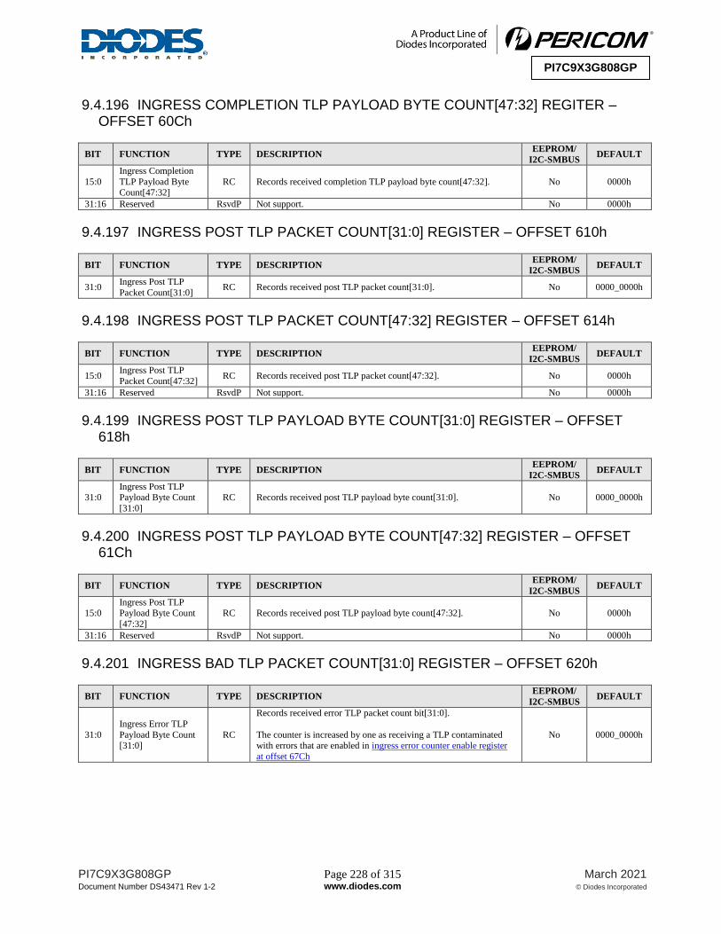
PI7C9X3G808GP Page 228 of 315 March 2021
Document Number DS43471 Rev 1-2 www.diodes.com © Diodes Incorporated
PI7C9X3G808GP
9.4.196 INGRESS COMPLETION TLP PAYLOAD BYTE COUNT[47:32] REGITER – OFFSET 60Ch
BIT FUNCTION TYPE DESCRIPTION EEPROM/
I2C-SMBUS DEFAULT
15:0
Ingress Completion
TLP Payload Byte Count[47:32]
RC Records received completion TLP payload byte count[47:32]. No 0000h
31:16 Reserved RsvdP Not support. No 0000h
9.4.197 INGRESS POST TLP PACKET COUNT[31:0] REGISTER – OFFSET 610h
BIT FUNCTION TYPE DESCRIPTION EEPROM/
I2C-SMBUS DEFAULT
31:0 Ingress Post TLP
Packet Count[31:0] RC Records received post TLP packet count[31:0]. No 0000_0000h
9.4.198 INGRESS POST TLP PACKET COUNT[47:32] REGISTER – OFFSET 614h
BIT FUNCTION TYPE DESCRIPTION EEPROM/
I2C-SMBUS DEFAULT
15:0 Ingress Post TLP
Packet Count[47:32] RC Records received post TLP packet count[47:32]. No 0000h
31:16 Reserved RsvdP Not support. No 0000h
9.4.199 INGRESS POST TLP PAYLOAD BYTE COUNT[31:0] REGISTER – OFFSET 618h
BIT FUNCTION TYPE DESCRIPTION EEPROM/
I2C-SMBUS DEFAULT
31:0 Ingress Post TLP Payload Byte Count
[31:0]
RC Records received post TLP payload byte count[31:0]. No 0000_0000h
9.4.200 INGRESS POST TLP PAYLOAD BYTE COUNT[47:32] REGISTER – OFFSET 61Ch
BIT FUNCTION TYPE DESCRIPTION EEPROM/
I2C-SMBUS DEFAULT
15:0 Ingress Post TLP Payload Byte Count
[47:32]
RC Records received post TLP payload byte count[47:32]. No 0000h
31:16 Reserved RsvdP Not support. No 0000h
9.4.201 INGRESS BAD TLP PACKET COUNT[31:0] REGISTER – OFFSET 620h
BIT FUNCTION TYPE DESCRIPTION EEPROM/
I2C-SMBUS DEFAULT
31:0
Ingress Error TLP
Payload Byte Count [31:0]
RC
Records received error TLP packet count bit[31:0].
The counter is increased by one as receiving a TLP contaminated with errors that are enabled in ingress error counter enable register
at offset 67Ch
No 0000_0000h
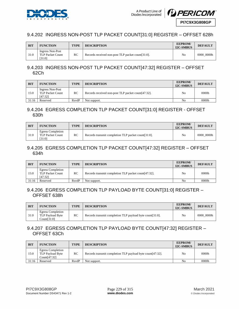
PI7C9X3G808GP Page 229 of 315 March 2021
Document Number DS43471 Rev 1-2 www.diodes.com © Diodes Incorporated
PI7C9X3G808GP
9.4.202 INGRESS NON-POST TLP PACKET COUNT[31:0] REGISTER – OFFSET 628h
BIT FUNCTION TYPE DESCRIPTION EEPROM/
I2C-SMBUS DEFAULT
31:0
Ingress Non-Post
TLP Packet Count [31:0]
RC Records received non-post TLP packet count[31:0]. No 0000_0000h
9.4.203 INGRESS NON-POST TLP PACKET COUNT[47:32] REGISTER – OFFSET 62Ch
BIT FUNCTION TYPE DESCRIPTION EEPROM/
I2C-SMBUS DEFAULT
15:0
Ingress Non-Post
TLP Packet Count [47:32]
RC Records received non-post TLP packet count[47:32]. No 0000h
31:16 Reserved RsvdP Not support. No 0000h
9.4.204 EGRESS COMPLETION TLP PACKET COUNT[31:0] REGISTER - OFFSET 630h
BIT FUNCTION TYPE DESCRIPTION EEPROM/
I2C-SMBUS DEFAULT
31:0
Egress Completion
TLP Packet Count [31:0]
RC Records transmit completion TLP packet count[31:0]. No 0000_0000h
9.4.205 EGRESS COMPLETION TLP PACKET COUNT[47:32] REGISTER – OFFSET 634h
BIT FUNCTION TYPE DESCRIPTION EEPROM/
I2C-SMBUS DEFAULT
15:0
Egress Completion
TLP Packet Count [47:32]
RC Records transmit completion TLP packet count[47:32]. No 0000h
31:16 Reserved RsvdP Not support. No 0000h
9.4.206 EGRESS COMPLETION TLP PAYLOAD BYTE COUNT[31:0] REGISTER – OFFSET 638h
BIT FUNCTION TYPE DESCRIPTION EEPROM/
I2C-SMBUS DEFAULT
31:0 Egress Completion TLP Payload Byte
Count[31:0]
RC Records transmit completion TLP payload byte count[31:0]. No 0000_0000h
9.4.207 EGRESS COMPLETION TLP PAYLOAD BYTE COUNT[47:32] REGISTER – OFFSET 63Ch
BIT FUNCTION TYPE DESCRIPTION EEPROM/
I2C-SMBUS DEFAULT
15:0 Egress Completion TLP Payload Byte
Count[47:32]
RC Records transmit completion TLP payload byte count[47:32]. No 0000h
31:16 Reserved RsvdP Not support. No 0000h

PI7C9X3G808GP Page 230 of 315 March 2021
Document Number DS43471 Rev 1-2 www.diodes.com © Diodes Incorporated
PI7C9X3G808GP
9.4.208 EGRESS POST TLP PACKET COUNT[31:0] REGISTER – OFFSET 640h
BIT FUNCTION TYPE DESCRIPTION EEPROM/
I2C-SMBUS DEFAULT
31:0 Egress Post TLP
Packet Count[31:0] RC Records transmit post TLP packet count[31:0] No 0000_0000h
9.4.209 EGRESS POST TLP PACKET BYTE COUNT[47:32] REGISTER – OFFSET 644h
BIT FUNCTION TYPE DESCRIPTION EEPROM/
I2C-SMBUS DEFAULT
15:0 Egress Post TLP Packet Count[47:32]
RC Records transmit post TLP packet count[47:32]. No 0000h
31:16 Reserved RsvdP Not support. No 0000h
9.4.210 EGRESS POST TLP PAYLOAD BYTE COUNT[31:0] REGISTER – OFFSET 648h
BIT FUNCTION TYPE DESCRIPTION EEPROM/
I2C-SMBUS DEFAULT
31:0 Egress Post TLP Payload Byte Count
[31:0]
RC Records transmit post TLP payload byte count[31:0]. No 0000_0000h
9.4.211 EGRESS POST TLP PAYLOAD BYTE COUNT[47:32] REGISTER – OFFSET 64Ch
BIT FUNCTION TYPE DESCRIPTION EEPROM/
I2C-SMBUS DEFAULT
8:0 Egress Post TLP Payload Byte Count
[47:32]
RC Records transmit post TLP payload byte count[47:32]. No 0000h
31:15 Reserved RsvdP Not support. No 0000h
9.4.212 EGRESS ERROR TLP PACKET COUNT[15:0] REGISTER – OFFSET 650h
BIT FUNCTION TYPE DESCRIPTION EEPROM/
I2C-SMBUS DEFAULT
15:0
Egress Error TLP
Payload Byte Count [15:0]
RC
Records transmit error TLP packet count[15:0].
A switch internal error such as ECC non-correctable error is detected when the packet reaches an egress port.
No 0000h
9.4.213 EGRESS ERROR TLP PAYLOAD BYTE COUNT[47:32] REGISTER – OFFSET 654h
BIT FUNCTION TYPE DESCRIPTION EEPROM/
I2C-SMBUS DEFAULT
8:0
Egress Error TLP
Payload Byte Count [47:32]
RC Records transmit error TLP payload byte count[47:32]. No 0000h
31:15 Reserved RsvdP Not support. No 0000h

PI7C9X3G808GP Page 231 of 315 March 2021
Document Number DS43471 Rev 1-2 www.diodes.com © Diodes Incorporated
PI7C9X3G808GP
9.4.214 EGRESS NON-POST TLP PACKET COUNT[31:0] REGISTER – OFFSET 658h
BIT FUNCTION TYPE DESCRIPTION EEPROM/
I2C-SMBUS DEFAULT
31:0
Egress Non-Post
TLP Packet Count [31:0]
RC Records transmit non-post TLP packet count[31:0]. No 0000_0000h
9.4.215 EGRESS NON-POST TLP PACKET COUNT[47:32] REGISTER – OFFSET 65Ch
BIT FUNCTION TYPE DESCRIPTION EEPROM/
I2C-SMBUS DEFAULT
15:0
Egress Non-Post
TLP Packet Count[47:32]
RC Records transmit non-post TLP packet count bit[47:32]. No 0000h
31:16 Reserved RsvdP Not support. No 0000h
9.4.216 TL/DLL/MAC/PHY ERROR TYPE SEL REGISTER – OFFSET 660h
BIT FUNCTION TYPE DESCRIPTION EEPROM/
I2C-SMBUS DEFAULT
7:0 Reg_664h_Sel RW
bit[1:0]: Reg_664h_Sel_Type
00b… Reg_664h_Sel[7:2] are used as dll_mac_err_sel_0[5:0] 01b… Reg_664h_Sel[7:2] are used as tl_err_sel_0[5:0]
10b… Reg_664h_Sel[7:2] are used as noc_err_sel_0[5:0] 11b…Reserved
dll_mac_err_sel_x[5:0] (x=0, 1 or 2): 00h… seq_err
01h… fcfail_retrain 02h… retry buffer full
03h… retry buffer ecc one bit error
04h… retry buffer ecc two bit error 05h… tx nullify
06h… replay timer expired 07h… replay no roll over
08h… retrain link
09h… nack seq_err 0Ah… tlp tx fifo length error (tlp tx protocol error (redundant
sof/eof, length error...) 0Bh… tlp tx fifo abort
0Ch… tlp tx header error
0Dh… tlp tx no EOF error 0Eh… crc16 error
0Fh… crc32 error 10h… nullify crc detect
11h… receive packet abort(tlp_rx_abort = 1)
12h… receive nack 13h… framing error
14h… retrain link 15h… recv_ts_speed_change
16h… recv_hot_reset_bit
17h… recv_disable_link 18h… recv_loopback
19h… recv_dis_screamb
1Ah… recv_comp 1Bh… goto retrain by MAC
1Ch… goto retrain by DUT LTSSM
1Dh… goto retrain by root
1Eh... PHY status error
1Fh~3Eh… reserved 3Fh… wrire or errors that corresponding mask bit set to 0 in
TL/DLL/MAC/PHY ERROR MASK 0 register
Yes 76h

PI7C9X3G808GP Page 232 of 315 March 2021
Document Number DS43471 Rev 1-2 www.diodes.com © Diodes Incorporated
PI7C9X3G808GP
BIT FUNCTION TYPE DESCRIPTION EEPROM/
I2C-SMBUS DEFAULT
7:0 Reg_664h_Sel RW
tl_err_sel_x[5:0] (x=0, 1 or 2): 00h…TL_ERR_STA[0]
01h…TRAIN_ERR_SET 02h…DLLP_ERR_SET
03h…RX_ERR_SET
04h…BAD_TLP_SET 05h…BAD_DLLP_SET
06h…REPLAY_ROLLOVER_SET 07h…REPLAY_TIMEOUT_SET
08h…UR_ERR_SET_all
09h…ECRC_ERR_SET_all 0Ah…MF_TLP_ERR_SET_all
0Bh…RX_OVERFLOW_SET 0Ch…UC_STS_SET_all
0Dh…FC_ERR_SET_all
0Eh…POISON_TLP_SET_all 0Fh… TL_ECC[0] (P/NP/CPLD buffer 1 bit ecc error OR)
10h… TL_ECC[1] (P/NP/CPLD buffer 1 bit ecc error OR) 11h~12h… Reserved
13h…TL_ERR_STA[1]
14h…TL_ERR_STA[2] 15h…TL_ERR_STA[3]
16h~3Eh… Reserved 3Fh…wire or errors that corresponding mask bit set to 0 in
TL/DLL/MAC/PHY ERROR MASK 0 register
noc_err_sel_x[5:0] (x=0, 1 or 2):
00h~01h… r_buffer one/two bit ecc error
02h~03h… v_buffer one/two bit ecc error
04h~05h… l_buffer one/two bit ecc error
06h~07h… d_buffer one/two bit ecc error 08h~09h… dma noc r_buffer one/two bit ecc error
0Ah~0Bh… dma noc v_buffer one/two bit ecc error 0Ch~0Dh… dma noc l_buffer one/two bit ecc error
0Eh~0Fh… dma noc d_buffer one/two bit ecc error
10h~1Dh… reserved 1Eh… eeprom_done
1Fh… strapin_transfer_time_out 20h~3Eh… reserved
3Fh… wire or errors that corresponding mask bit set to 0 in
TL/DLL/MAC/PHY ERROR MASK 0 register
Yes 76h
15:8 Reg_668h_Sel RW
bit[1:0]: Reg_668h_Sel_Type.
00b… Reg_668h_Sel[15:10] are used as dll_mac_err_sel_1[5:0]
01b… Reg_668h_Sel[15:10] are used as tl_err_sel_1[5:0]
10b… Reg_668h_Sel[15:10] are used as noc_err_sel_1[5:0]
11b…Reserved
If Reg_668h_Sel[15:10] = 3Fh, wire or errors that corresponding
mask bit set to 0 in TL/DLL/MAC/PHY ERROR MASK 1 register
Yes 76h
23:16 Reg_66Ch_Sel RW
bit[1:0]: Reg_66Ch_Sel_Type.
00b… Reg_66Ch_Sel[23:18] are used as dll_mac_err_sel_2[5:0]
01b… Reg_66Ch_Sel[23:18] are used as tl_err_sel_2[5:0] 10b… Reg_66Ch_Sel[23:18] are used as noc_err_sel_2[5:0]
11b…Reserved
If Reg_66Ch_Sel[23:18] = 3Fh, wire or errors that corresponding
mask bit set to 0 in TL/DLL/MAC/PHY ERROR MASK 2 register
Yes 76h
31:24 Reserved RsvdP Not support. No 00h
9.4.217 TL/DLL/MAC/PHY ERROR COUNT 0 REGISTER – OFFSET 664h
BIT FUNCTION TYPE DESCRIPTION EEPROM/
I2C-SMBUS DEFAULT
15:0 TL/DLL/MAC/PHY
Error Count 0 RW1C TL/DLL/MAC/PHY Error count 0. Yes 0000h

PI7C9X3G808GP Page 233 of 315 March 2021
Document Number DS43471 Rev 1-2 www.diodes.com © Diodes Incorporated
PI7C9X3G808GP
9.4.218 TL/DLL/MAC/PHY ERROR COUNT 1 REGISTER – OFFSET 668h
BIT FUNCTION TYPE DESCRIPTION EEPROM/
I2C-SMBUS DEFAULT
15:0 TL/DLL/MAC/PHY
Error Count 1 RW1C TL/DLL/MAC/PHY Error count 1. Yes 0000h
9.4.219 TL/DLL/MAC/PHY ERROR COUNT 2 REGISTER – OFFSET 66Ch
BIT FUNCTION TYPE DESCRIPTION EEPROM/
I2C-SMBUS DEFAULT
15:0 TL/DLL/MAC/PHY
Error Count 2 RW1C TL/DLL/MAC/PHY Error count 2. Yes 0000h
9.4.220 TL/DLL/MAC/PHY ERROR MASK 0 REGISTER – OFFSET 670h
BIT FUNCTION TYPE DESCRIPTION EEPROM/
I2C-SMBUS DEFAULT
31:0 Reg_664 Error Mask RW For reg_664_sel[7:2]==6'h3f error mask purpose. Yes 0000_0000h
9.4.221 TL/DLL/MAC/PHY ERROR MASK 1 REGISTER – OFFSET 674h
BIT FUNCTION TYPE DESCRIPTION EEPROM/
I2C-SMBUS DEFAULT
31:0 Reg_668 Error Mask RW For reg_668_sel[7:2]==6'h3f error mask purpose. Yes 0000_0000h
9.4.222 TL/DLL/MAC/PHY ERROR MASK 2 REGISTER – OFFSET 678h
BIT FUNCTION TYPE DESCRIPTION EEPROM/
I2C-SMBUS DEFAULT
31:0 Reg_66C Error Mask RW For reg_66C_sel[7:2]==6'h3f error mask purpose. Yes 0000_0000h
9.4.223 INGRESS ERROR COUNTER ENABLE REGISTER – OFFSET 67Ch
BIT FUNCTION TYPE DESCRIPTION EEPROM/
I2C-SMBUS DEFAULT
0 Training Error
Enable RW
When set, the Training Error event is counted in ingress bad TLP
packet counter at offset 620H. Yes 0
1 Reserved RsvdP Not support. No 0
2 MWR Error Enable RW When set, the Memory write error event is counted in ingress bad
TLP packet counter at offset 620H. Yes 1
3 MRD Error Enable RW When set, the Memory read clpd error event is counted in ingress bad TLP packet counter at offset 620H.
Yes 1
4 Data Link Protocol
Error Enable RW
When set, the Data Link Protocol Error event is counted in ingress
bad TLP packet counter at offset 620H. Yes 0
5 Surprise Down Error Enable
RW When set, Surprise Down Error event is counted in ingress bad TLP packet counter at offset 620H.
Yes 0
11:6 Reserved RsvdP Not support. Yes 0
12 Poisoned TLP Enable
RW When set, an event of Poisoned TLP is counted in ingress bad TLP packet counter at offset 620H.
Yes 0
13
Flow Control
Protocol Error Enable
RW When set, the Flow Control Protocol Error event is counted in
ingress bad TLP packet counter at offset 620H. Yes 0
14 Completion Timeout
Enable RW
When set, the Completion Timeout event is counted in ingress bad
TLP packet counter at offset 620H. Yes 0
15 Completer Abort
Enable RW
When set, the Completer Abort event is counted in ingress bad TLP
packet counter at offset 620H. Yes 0
16 Unexpected Completion Enable
RW When set, the Unexpected Completion event is counted in ingress bad TLP packet counter at offset 620H.
Yes 0

PI7C9X3G808GP Page 234 of 315 March 2021
Document Number DS43471 Rev 1-2 www.diodes.com © Diodes Incorporated
PI7C9X3G808GP
BIT FUNCTION TYPE DESCRIPTION EEPROM/
I2C-SMBUS DEFAULT
17 Receiver Overflow Enable
RW When set, the Receiver Overflow event is counted in ingress bad TLP packet counter at offset 620H.
Yes 0
18 Malformed TLP
Enable RW
When set, an event of Malformed TLP is counted in ingress bad
TLP packet counter at offset 620H. Yes 0
19 ECRC Error Enable RW When set, an event of ECRC Error is counted in ingress bad TLP
packet counter at offset 620H. Yes 0
20 Unsupported Request Error Enable
RW When set, the Unsupported Request event is counted in ingress bad TLP packet counter at offset 620H.
Yes 0
21 ACS Violation
Enable RW
When set, the ACS Violation event is counted in ingress bad TLP
packet counter at offset 620H. Yes 0
22 Reserved RsvdP Not support. Yes 0
23 MC Blocked TLP
Enable RW
When set, the MC Blocked TLP event is counted in ingress bad
TLP packet counter at offset 620H. Yes 0
24 AtomicOp Egress Blocked Enable
RW When set, the AtomicOp Egress Blocked event is counted in ingress bad TLP packet counter at offset 620H.
Yes 0
25 Bad TLP Enable RW When set, the event of Bad TLP has been received is counted in ingress bad TLP packet counter at offset 620H.
Yes 0
26 Bad DLLP Enable RW When set, the event of Bad DLLP has been received is counted in
ingress bad TLP packet counter at offset 620H. Yes 0
27 REPLAY_NUM Rollover Enable
RW When set, the REPLAY_NUM Rollover event is counted in ingress bad TLP packet counter at offset 620H.
Yes 0
28 Replay Timer
Timeout Enable RW
When set, the Replay Timer Timeout event is counted in ingress
bad TLP packet counter at offset 620H. Yes 0
29 Advisory Non-Fatal
Error Enable RW
When set, the Advisory Non-Fatal Error event is counted in ingress
bad TLP packet counter at offset 620H. Yes 0
30 One bit ECC Error Enable
RW When set, the One-bit ECC Error event is counted in ingress bad TLP packet counter at offset 620H.
Yes 0
31 Two bit ECC Error
Enable RW
When set, the Two-bit ECC Error event is counted in ingress bad
TLP packet counter at offset 620H. Yes 1
9.4.224 TRIGGER 1 MASK REGISTER – OFFSET 700h (Port 0 Only)
BIT FUNCTION TYPE DESCRIPTION EEPROM/
I2C-SMBUS DEFAULT
31:0 Trigger 1 Mask RW Set “1” to enable corresponding offset 708h bits. Yes 0000_0000h
9.4.225 TRIGGER 2 MASK REGISTER – OFFSET 704h (Port 0 Only)
BIT FUNCTION TYPE DESCRIPTION EEPROM/
I2C-SMBUS DEFAULT
31:0 Trigger 2 Mask RW Set “1” to enable corresponding offset 70Ch bits. Yes 0000_0000h
9.4.226 PATTERN 1 SETTING REGISTER – OFFSET 708h (Port 0 Only)
BIT FUNCTION TYPE DESCRIPTION EEPROM/
I2C-SMBUS DEFAULT
31:0 Pattern 1 Setting RW Set bit[31:0] pattern to match internal selected debug_out[31:0] by
offset 710h. Yes 0000_0000h
9.4.227 PATTERN 2 SETTING REGISTER – OFFSET 70Ch (Port 0 Only)
BIT FUNCTION TYPE DESCRIPTION EEPROM/
I2C-SMBUS DEFAULT
31:0 Pattern 2 Setting RW Set bit[31:0] pattern to match internal selected debug_out[31:0] by offset 714h.
Yes 0000_0000h

PI7C9X3G808GP Page 235 of 315 March 2021
Document Number DS43471 Rev 1-2 www.diodes.com © Diodes Incorporated
PI7C9X3G808GP
9.4.228 TRIGGER 1 DEBUG_OUT MODE SELECTION REGISTER – OFFSET 710h (Port 0 Only)
BIT FUNCTION TYPE DESCRIPTION EEPROM/
I2C-SMBUS DEFAULT
4:0 Mode 1 Setting RW
Used as debug_out mode_sel[4:0].
When offset 390h.bit[31]=0 (embedded LA)
bit[4]=0, used for MAC debug out signals
bit[4]=1 and bit[3:0]=0~14 are used for TLP debug out signals bit[4]=1 and bit[3:0]=15 are used for power saving debug signals
When offset 390h.bit[31]=1 (LTSSM flow)
bit[4] is used to reset read/write counter
Yes 0_0000b
7:5 Reserved RsvdP Not support. No 000b
13:8 Trigger 1 port Selection
RW Used to set trigger 1 port. Yes 00_0000b
31:14 Reserved RsvdP Not support. No 0_0h
9.4.229 TRIGGER 2 DEBUG_OUT MODE SELECTION REGISTER – OFFSET 714h (Port 0 Only)
BIT FUNCTION TYPE DESCRIPTION EEPROM/
I2C-SMBUS DEFAULT
4:0 Mode 2 Setting RW Used as debug_out mode_sel[4:0]. Yes 0_0000b
7:5 Reserved RsvdP Not support. No 000b
13:8 Trigger 2 port
selection RW Used to set trigger 2 port. Yes 00_0000b
31:14 Reserved RsvdP Not support. No 0_0h
9.4.230 TRIGGER 1 AND/OR CONDITION SELECTION REGISTER – OFFSET 718h (Port 0 Only)
BIT FUNCTION TYPE DESCRIPTION EEPROM/
I2C-SMBUS DEFAULT
0 And/Or Select 1 RW 0b: OR logical for trigger 1 1b: AND logical for trigger 1
Yes 1
31:1 Reserved RsvdP Not support. No 0_0h
9.4.231 TRIGGER 2 AND/OR CONDITION SELECTION REGISTER – OFFSET 71Ch (Port 0 Only)
BIT FUNCTION TYPE DESCRIPTION EEPROM/
I2C-SMBUS DEFAULT
0 And/Or Select 2 RW 0b: OR logical for trigger 1 1b: AND logical for trigger 1
Yes 1
31:1 Reserved RsvdP Not support. No 0_0h
9.4.232 TRIGGER SELECT REGISTER – OFFSET 720h (Port 0 Only)
BIT FUNCTION TYPE DESCRIPTION EEPROM/
I2C-SMBUS DEFAULT
2:0 Trigger Select RW
000b: select offset 708h trigger pattern as trigger 001b: select offset 70Ch trigger pattern as trigger
010b: select offset 708h and 70Ch trigger patterns as trigger
011b: select offset 708h or 70Ch trigger pattern as trigger 100b: if offset 708h match then go to offset 70Ch trigger pattern
Others: Reserved
Yes 000b
7:3 Reserved RsvdP Not support. No 0000_0b
10:8 External port trigger RW Internal used only. Yes 000b
31:11 Reserved RsvdP Not support. No 0_0h

PI7C9X3G808GP Page 236 of 315 March 2021
Document Number DS43471 Rev 1-2 www.diodes.com © Diodes Incorporated
PI7C9X3G808GP
9.4.233 TRIGGER POSITION SELECTION REGISTER – OFFSET 724h (Port 0 Only)
BIT FUNCTION TYPE DESCRIPTION EEPROM/
I2C-SMBUS DEFAULT
6:0 Trigger Position
Select RW
Used to select the trigger address, where 00h is from header (0%)
and 7Fh is ending (100%). Yes 20h
31:7 Reserved RsvdP Not support. No 0_0h
9.4.234 TRIGGER COUNTER SETTING REGISTER – OFFSET 72Ch (Port 0 Only)
BIT FUNCTION TYPE DESCRIPTION EEPROM/
I2C-SMBUS DEFAULT
3:0 Counter RW Used to set trigger amount when trigger achieves the trigger count. Yes 0h
31:4 Reserved RsvdP Not support. No 0000_000h
9.4.235 TRIGGER START REGISTER – OFFSET 730h (Port 0 Only)
BIT FUNCTION TYPE DESCRIPTION EEPROM/
I2C-SMBUS DEFAULT
0 Trigger Start RW When set, start the trigger. Yes 0
1 Debug_to_use_LA_ en
RW When set, enable debug to use LA. Yes 0
15:1 Reserved RsvdP Not support. No 0-0b
29:16 Cycle Left RO Show how many cycles left. No 3FFFh
31:30 Reserved RsvdP Not support. No 00b
9.4.236 READ WAVEFORM DATA REGISTER – OFFSET 734h (Port 0 Only)
BIT FUNCTION TYPE DESCRIPTION EEPROM/
I2C-SMBUS DEFAULT
31:0 Read Waveform
Data RO
Used tooutput embedded debug memory data.
Total 4096 cycles can be read and read out is in sequence from
cycle 0. Each offset 734h read command will advance 1 cycle
automatically.
No 0000_0000h
9.4.237 SAMPLE RATE SETTING REGISTER – OFFSET 738h (Port 0 Only)
BIT FUNCTION TYPE DESCRIPTION EEPROM/
I2C-SMBUS DEFAULT
3:0 Sample Rate Setting RW
Used to set the embedded LA sampling rate.
0h: 500MHz sampling rate 1h: 250MHz sampling rate
2h: 125MHz sampling rate
…
Yes 0000_0000h
31:4 Reserved RsvdP Not support. No 0-0h
9.4.238 WAVEFORM OUTPUT PORT SELECT REGISTER – OFFSET 73Ch (Port 0 Only)
BIT FUNCTION TYPE DESCRIPTION EEPROM/
I2C-SMBUS DEFAULT
5:0 Waveform Output
Port Select RW
Used to select which port’s debug_out[31:0] can be dumped into
embedded debug memory. Yes 00_0000b
7:6 Reserved RsvdP Not support. No 0-0h
12:8 Waveform Output
Model_Sel Select RW
Used to select which model_sel[4:0] debug_out can be dumped into
embedded debug memory. Yes 0-0b
15:13 Reserved RsvdP Not support. No 000b

PI7C9X3G808GP Page 237 of 315 March 2021
Document Number DS43471 Rev 1-2 www.diodes.com © Diodes Incorporated
PI7C9X3G808GP
BIT FUNCTION TYPE DESCRIPTION EEPROM/
I2C-SMBUS DEFAULT
16 Switch Output Singal Source
RW When set, it will switch debug_mode GPIO[31:0] output signal source from internal debug_out to debug memory stored debug_out
data.
Yes 0
17 Enable User-Defined Mode
RW When set, it will select internal debug_out port_sel/mode_sel to bit[5:0]/bit[12:8] port_sel/mode_sel value.
Yes 0
18 PORT_GOOD Setting
RW When set, it will switch PORT_GOOD_L[7:0] output from original link status to internal error status.
Yes 0
31:19 Reserved RsvdP Not support. No 0-0h
9.4.239 WAVEFORM READ EVENT RESET REGISTER – OFFSET 748h (Port 0 Only)
BIT FUNCTION TYPE DESCRIPTION EEPROM/
I2C-SMBUS DEFAULT
0 Back to waveform by
CFG/I2C/SMBUS WO
When set, the read point will back to the header of the waveform.
Reading returns 0 always.
Yes 0
31:1 Reserved RsvdP Not support. No 0-0h
9.4.240 DUMP MEMORY TO GPIO RATE CONTROL REGISTER – OFFSET 74Ch (Port 0 Only)
BIT FUNCTION TYPE DESCRIPTION EEPROM/
I2C-SMBUS DEFAULT
3:0
Dump Waveform to
LA Sample Rate Setting
RW
Used to set the debug memory 32 bits data output to GPIO[31:0] rate.
0h: output to GPIO[31:0] as 500MHz clock rate 1h: output to GPIO[31:0] as 250HHz clock rate
2h: output to GPIO[31:0] as 125MHz clock rate …
Yes 0h
31:4 Reserved RsvdP Not support. No 0-0h
9.4.241 DUMP WAVEFORM START REGISTER – OFFSET 750h (Port 0 Only)
BIT FUNCTION TYPE DESCRIPTION EEPROM/
I2C-SMBUS DEFAULT
0 Dump Waveform
Start RW When set, start to dump waveform to LA. Yes 0
31:1 Reserved RsvdP Not support. No 0-0h
9.4.242 FREE RUN BUTTON REGISTER – OFFSET 754h (Port 0 Only)
BIT FUNCTION TYPE DESCRIPTION EEPROM/
I2C-SMBUS DEFAULT
0 Free Run Button RW When set, debug memory will store pre-defined internal
debug_out[31:0] data, and output to GPIO[31:0] automatically. Yes 0
31:1 Reserved RsvdP Not support. No 0-0h
9.4.243 VENDOR SPECIFIC CAPABILITIES REGISTER – OFFSET 900h
BIT FUNCTION TYPE DESCRIPTION EEPROM/
I2C-SMBUS DEFAULT
15:0 Extended
Capabilities ID RO
Read as 000Bh to indicate that this is PCI express extended
capability register for vendor specific. No 000Bh
19:16 Capability Version RO Read as 1h. No 1h
31:20 Next Capability
Offset RO Read as 000h. No other ECP registers. Yes 000h
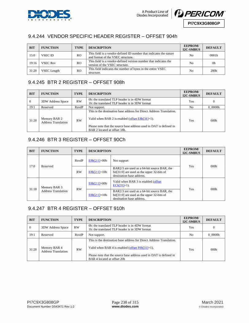
PI7C9X3G808GP Page 238 of 315 March 2021
Document Number DS43471 Rev 1-2 www.diodes.com © Diodes Incorporated
PI7C9X3G808GP
9.4.244 VENDOR SPECIFIC HEADER REGISTER – OFFSET 904h
BIT FUNCTION TYPE DESCRIPTION EEPROM/
I2C-SMBUS DEFAULT
15:0 VSEC ID RO This field is a vendor-defined ID number that indicates the nature
and format of the VSEC structure. No 0001h
19:16 VSEC Rev RO This field is a vendor-defined version number that indicates the version of the VSEC structure.
No 0h
31:20 VSEC Length RO This field indicates the number of bytes in the entire VSEC
structure. No 280h
9.4.245 BTR 2 REGISTER – OFFSET 908h
BIT FUNCTION TYPE DESCRIPTION EEPROM/
I2C-SMBUS DEFAULT
0 3DW Address Space RW 0b: the translated TLP header is in 4DW format
1b: the translated TLP header is in 3DW format Yes 0
19:1 Reserved RsvdP Not support. No 0_0000h
31:20 Memory BAR 2 Address Translation
RW
This is the destination base address for Direct Address Translation.
Valid when BAR 2 is enabled (offset E8h[31]=1).
Please note that the source base address used in DAT is defined in
BAR 2 located at offset 18h.
Yes 000h
9.4.246 BTR 3 REGISTER – OFFSET 90Ch
BIT FUNCTION TYPE DESCRIPTION EEPROM/
I2C-SMBUS DEFAULT
17:0 Reserved
RsvdP E8h[2:1]=00b Not support
Yes 000h
RW E8h[2:1]=10b BAR2/3 are used as a 64-bit source BAR, the bit[31:0] are used as the upper 32-bits of
destination base address.
31:18 Memory BAR 3
Address Translation RW
E8h[2:1]=00b Valid when BAR 3 is enabled (offset
ECh[31]=1).
Yes 000h
E8h[2:1]=10b
BAR2/3 are used as a 64-bit source BAR, the
bit[31:0] are used as the upper 32-bits of destination base address.
9.4.247 BTR 4 REGISTER – OFFSET 910h
BIT FUNCTION TYPE DESCRIPTION EEPROM/
I2C-SMBUS DEFAULT
0 3DW Address Space RW 0b: the translated TLP header is in 4DW format
1b: the translated TLP header is in 3DW format Yes 0
19:1 Reserved RsvdP Not support. No 0_0000h
31:20 Memory BAR 4
Address Translation RW
This is the destination base address for Direct Address Translation.
Valid when BAR 4 is enabled (offset F0h[31]=1).
Please note that the source base address used in DAT is defined in
BAR 4 located at offset 20h
Yes 000h

PI7C9X3G808GP Page 239 of 315 March 2021
Document Number DS43471 Rev 1-2 www.diodes.com © Diodes Incorporated
PI7C9X3G808GP
9.4.248 BTR 5 REGISTER – OFFSET 914h
BIT FUNCTION TYPE DESCRIPTION EEPROM/
I2C-SMBUS DEFAULT
19:0 Reserved
RsvdP F0h[2:1]=00b Not support.
No/Yes 000h
RW F0h[2:1]=10b BAR4/5 are used as a 64-bit source BAR, the bit[31:0] are used as the upper 32-bits of
destination base address.
31:20 Memory BAR 5
Address Translation RW
F0h[2:1]=00b Valid when BAR 5 is enabled (offset F4h[31]=1).
Yes 000h
F0h[2:1]=10b BAR4/5 are used as a 64-bit source BAR, the bit[31:0] are used as the upper 32-bits of
destination base address.
9.4.249 ADDRESS LUT ACCESS ADDRESS REGISTER – OFFSET 918h
BIT FUNCTION TYPE DESCRIPTION EEPROM/
I2C-SMBUS DEFAULT
6:0 Index RW
Used to indicate the LUT Entry number.
In Generic CDLEP mode, all of entries (128) are allocated for
address translation based upon BAR2/3.
Yes 00h
7 Reserved RsvdP Not support. No 0b
8 Command WO
0b: Read command
1b: Write command
Return ‘0’ when read always.
Yes 0
31: 9 Reserved RsvdP Not support No 0-0h
9.4.250 ADDRESS LUT ACCESS DATA 0 REGISTER – OFFSET 91Ch
BIT FUNCTION TYPE DESCRIPTION EEPROM/
I2C-SMBUS DEFAULT
0 3DW Address Space RW 0b: the translated TLP header is in 4DW format 1b: the translated TLP header is in 3DW format
Yes 0
4:1 Domain Number RW Used to indicate the destination port’s domain number. Yes 0000b
12:5 Reserved RsvdP Not support No 0-0b
31:13 LUT Data[18:0] RW Used to indicate the destination base address for address translation in 32-bit address domain.
Yes 0-0h
9.4.251 ADDRESS LUT ACCESS DATA 1 REGISTER – OFFSET 920h
BIT FUNCTION TYPE DESCRIPTION EEPROM/
I2C-SMBUS DEFAULT
31:0 LUT HData[31:0] RW Used to indicate the higher 32-bit destination base address in 64-bit
address domain. Yes 0000_0000h
9.4.252 REQ ID/DOMAIN LUT 0 – 15– OFFSET 924h to 960h
These 16 32-bit registers construct a Requester ID (RID) look-up table storing the RID of TLP issued from Local host,
which connected to the CDLEP port directly. The table content can be either built by hardware automatically or written
by software of management CPU. There arecontrol signals defined in the 14th
and 15th
bits of Device Configuration 2
Register at offset 50Ch of Port 0 to decide RID LUT build-up mechanism for CDLEP P0 and CDLEP P4 respectively.
Table 9-6: 16-Bit REQ ID/Domain LUT Entry 0-63 Register Locations CFG_OFFSET ID/DomainLUT Entry_n CFG_OFFSET ID/Domain LUT Entry_n
924h 0 944h 8
928h 1 948h 9

PI7C9X3G808GP Page 240 of 315 March 2021
Document Number DS43471 Rev 1-2 www.diodes.com © Diodes Incorporated
PI7C9X3G808GP
CFG_OFFSET ID/DomainLUT Entry_n CFG_OFFSET ID/Domain LUT Entry_n
92Ch 2 94Ch 10
930h 3 950h 11
934h 4 954h 12
938h 5 958h 13
93Ch 6 95Ch 14
940h 7 960h 15
Table 9-7: 16-Bit REQ ID/Domain LUT Entry_n (n=0 through 15)
BIT FUNCTION TYPE DESCRIPTION EEPROM/
I2C-SMBUS DEFAULT
15:0 ReqID RW 50Ch[14] / 50Ch[15] = 0 bit[2:0]: function number
bit[7:3]: device number
bit[15:8]: bus number
Yes 0000h RO 50Ch[14] / 50Ch[15] = 1
30:16 Reserved RsvdP Not support. No 0-0b
31 Valid RW 50Ch[14] / 50Ch[15] = 0 0b: the entry is not valid
1b: the entry is valid Yes 0
RO 50Ch[14] / 50Ch[15] = 1
9.4.253 CAPTURED BUS ID for DOMAIN 0 to 3 – OFFSET 994h
BIT FUNCTION TYPE DESCRIPTION EEPROM/
I2C-SMBUS DEFAULT
7:0 Dom. 0 Bus Number RW To set the captured bus number for Domain 0 as a destination Bus Number in RID translation.
Yes 00h
15:8 Dom 1 Bus Number RW To set the captured bus number for Domain 1 as a destination Bus
Number in RID translation. Yes 00h
23:16 Dom. 2 Bus Number RW To set the captured bus number for Domain 2 as a destination Bus Number in RID translation.
Yes 00h
31:24 Dom 3 Bus Number RW To set the captured bus number for Domain 3 as a destination Bus
Number in RID translation. Yes 00h
9.4.254 CAPTURED BUS ID for DOMAIN 4 to 7 – OFFSET 998h
BIT FUNCTION TYPE DESCRIPTION EEPROM/
I2C-SMBUS DEFAULT
7:0 Dom. 4 Bus Number RW To set the captured bus number for Domain4 as a destination Bus
Number in RID translation. Yes 00h
15:8 Dom. 5 Bus Number RW To set the captured bus number for Domain5 as a destination Bus Number in RID translation.
Yes 00h
23:16 Dom. 6 Bus Number RW To set the captured bus number for Domain6 as a destination Bus
Number in RID translation. Yes 00h
31:24 Dom. 7 Bus Number RW To set the captured bus number for Domain7 as a destination Bus Number in RID translation.
Yes 00h
9.4.255 CAPTURED BUS ID for DOMAIN 8 to 11 – OFFSET 99Ch
BIT FUNCTION TYPE DESCRIPTION EEPROM/
I2C-SMBUS DEFAULT
7:0 Dom. 8 Bus Number RW To set the captured bus number for Domain8 as a destination Bus
Number in RID translation. Yes 00h
15:8 Dom. 9 Bus Number RW To set the captured bus number for Domain9 as a destination Bus
Number in RID translation. Yes 00h
23:16 Dom. 10 Bus Number
RW To set the captured bus number for Domain10 as a destination Bus Number in RID translation.
Yes 00h
31:24 Dom. 11 Bus
Number RW
To set the captured bus number for Domain11 as a destination Bus
Number in RID translation. Yes 00h
9.4.256 DOOR BELL IRQ SET REGISTER – OFFSET 9C4h
BIT FUNCTION TYPE DESCRIPTION EEPROM/
I2C-SMBUS DEFAULT
31:0 Set IRQ RW1S Set link interface IRQ.
Yes 0000_0000h

PI7C9X3G808GP Page 241 of 315 March 2021
Document Number DS43471 Rev 1-2 www.diodes.com © Diodes Incorporated
PI7C9X3G808GP
BIT FUNCTION TYPE DESCRIPTION EEPROM/
I2C-SMBUS DEFAULT
If any of 32 bits is set and the corresponding bit in Door Bell IRQ register is not set, an interrupt will be issued in the link interface to
local host. Writing“0” to this register does not take any effect.
Interrupt can be in either INTx or MSI or MSI-X format depending
on how system enabling which type of interrupts mechanism.
9.4.257 DOOR BELL IRQ CLEAR REGISTER – OFFSET 9C8h
BIT FUNCTION TYPE DESCRIPTION EEPROM/
I2C-SMBUS DEFAULT
31:0 Clear IRQ RW1C
Clear link interface IRQ.
Writing“1” to the bit whose corresponding bit is set in 9C4h will clear the bit. If INTx mechanism is chosen, an INTx deassert
message will be generated.
Writing“0” to this register does not take any effect.
Yes 0000_0000h
9.4.258 DOOR BELL IRQ MASK SET REGISTER – OFFSET 9CCh
BIT FUNCTION TYPE DESCRIPTION EEPROM/
I2C-SMBUS DEFAULT
31:0 Set IRQ Mask RW1S
Set link interface interrupt IRQ mask.
Writing“1” to the bit whose corresponding bit in 9C4h for
generating interrupt will be masked out.
Writing“0” to this register does not take any effect.
Yes FFFF_FFFFh
9.4.259 DOOR BELL IRQ MASK CLEAR REGISTER – OFFSET 9D0h
BIT FUNCTION TYPE DESCRIPTION EEPROM/
I2C-SMBUS DEFAULT
31:0 Clear IRQ Mask RW1C
Clear link interface interrupt IRQ mask.
Writing “1” to the bit whose corresponding bit in 9C4h for generating interrupt will not be masked out.
Writing“0” to this register does not take any effect.
Yes FFFF_FFFFh
9.4.260 SCRATCHPAD 0 REGISTER – OFFSET 9E4h
BIT FUNCTION TYPE DESCRIPTION EEPROM/
I2C-SMBUS DEFAULT
31:0 Scratchpad 0 RW Scratchpad 0 register. Yes 0000_0000h
9.4.261 SCRATCHPAD 1 REGISTER – OFFSET 9E8h
BIT FUNCTION TYPE DESCRIPTION EEPROM/
I2C-SMBUS DEFAULT
31:0 Scratchpad 1 RW Scratchpad 1 register. Yes 0000_0000h
9.4.262 SCRATCHPAD 2 REGISTER – OFFSET 9ECh
BIT FUNCTION TYPE DESCRIPTION EEPROM/
I2C-SMBUS DEFAULT
31:0 Scratchpad 2 RW Scratchpad 2 register. Yes 0000_0000h

PI7C9X3G808GP Page 242 of 315 March 2021
Document Number DS43471 Rev 1-2 www.diodes.com © Diodes Incorporated
PI7C9X3G808GP
9.4.263 SCRATCHPAD 3 REGISTER – OFFSET 9F0h
BIT FUNCTION TYPE DESCRIPTION EEPROM/
I2C-SMBUS DEFAULT
31:0 Scratchpad 3 RW Scratchpad 3 register. Yes 0000_0000h
9.4.264 SCRATCHPAD 4 REGISTER – OFFSET 9F4h
BIT FUNCTION TYPE DESCRIPTION EEPROM/
I2C-SMBUS DEFAULT
31:0 Scratchpad 4 RW Scratchpad 4 register. Yes 0000_0000h
9.4.265 SCRATCHPAD 5 REGISTER – OFFSET 9F8h
BIT FUNCTION TYPE DESCRIPTION EEPROM/
I2C-SMBUS DEFAULT
31:0 Scratchpad 5 RW Scratchpad 5 register. Yes 0000_0000h
9.4.266 SCRATCHPAD 6 REGISTER – OFFSET 9FCh
BIT FUNCTION TYPE DESCRIPTION EEPROM/
I2C-SMBUS DEFAULT
31:0 Scratchpad 6 RW Scratchpad 6 register. Yes 0000_0000h
9.4.267 SCRATCHPAD 7 REGISTER – OFFSET A00h
BIT FUNCTION TYPE DESCRIPTION EEPROM/
I2C-SMBUS DEFAULT
31:0 Scratchpad 7 RW Scratchpad 7 register. Yes 0000_0000h
9.4.268 CDEP DATA 0 REGISTER – OFFSET A04h
BIT FUNCTION TYPE DESCRIPTION EEPROM/
I2C-SMBUS DEFAULT
7:0 Bus Number RO Used to save the bus number for the CDEP. No 00h
10:8 Reserved RsvdP Not support. No 000b
11 Reserved RsvdP Not support. No 0
15:12 Source Domain
Number RO Used to save the source domain number. No 0000b
17:16 CD Mode RO Used to save the status for Device Configuration CD Mode. No 00b
18 CDEP Status RO
Used to indicate CDEP status
1b: CDEP is enabled. 0b: CDEP is disabled
No 0
19 CDEP Type RO 0b: CDLEP
1b: CDVEP No 0
31:19 Reserved RsvdP Not support. No 0-0b
9.4.269 CDEP DATA 1 REGISTER – OFFSET A08h
BIT FUNCTION TYPE DESCRIPTION EEPROM/
I2C-SMBUS DEFAULT
15:0 L_Host Request ID RO Used to indate local host requester ID, which is captured during
enumeration. No 0000h
30:16 Reserved RsvdP Not support. No 0000h
31 CDEP link enabled RO
When set, the link between local host and CDLEP port is enabled.
Once link is up, the configuration and memory commands will be
sent to PRIMARY HOST via message queue or cross-domain translated transaction.
Yes 0

PI7C9X3G808GP Page 243 of 315 March 2021
Document Number DS43471 Rev 1-2 www.diodes.com © Diodes Incorporated
PI7C9X3G808GP
9.4.270 SQ/CQ POINTER CONTROL AND STATUS REGISTER – OFFSET A0Ch
BIT FUNCTION TYPE DESCRIPTION EEPROM/
I2C-SMBUS DEFAULT
1:0 SQ Depth RW
Notify CDLEP the depth of submission queue. The queue is
allocatded in the physical memory of PRIMARY HOST.
00: 8 entries 01: 16 entries
10: 32 entries
11: Not defined
No 00b
6:2 SQ Tail Index RO
Indicate the current Tail pointer maintained by CDLEP
For each transaction met the overlay range and converted into a message going out to PRIMARY HOST, the index will be increased
by one and finally reset to zero after hitting to the SQ depth.
No 00000b
10:7 SQ Buffer Fullness
Level RO
Indicate the current fullness levelin the SQ buffer located at CDLEP.
For any new message that written into the SQ buffer temporarily,
the level will be moved up by one. If the message read out from the
SQ buffer, the level will be moved down by one.When the value equals to “8h”, it means the SQ buffer is full.
No 0000b
15:11 Reserved RsvdP Not support. No 00h
19:16 MMIO_VAL
FIFOFullness Level RO
Indicate the current fullness level for MMIO_VAL FIFO located at CDLEP.
If the retured CQ message containing MMIO_VAL, it will be stored
in the MMIO_VAL FIFO temporarily and the index will be moved
up by one. If the message leaving the MMIO_VAL FIFO, the index will be moved down by one. When the value equals to “8h”, it
means the MMIO_VAL FIFO is full.
No 0000b
31:20 Reserved RsvdP Not support. No 000h
9.4.271 SQ TAIL BASE POINTER [31:0] REGISTER – OFFSET A10h
BIT FUNCTION TYPE DESCRIPTION EEPROM/
I2C-SMBUS DEFAULT
31:0 SQ Tail Base
Pointer_L RW
Point to the tail base location of SQ, bit[31:0].
PRIMARY HOST has toprogram its SQ tail pointer register, which is the base address of the SQ maintained by PRIMARY HOST. So
the switch can deliver the message to the correct location.
No 0000_0000h
9.4.272 SQ TAIL BASE POINTER [63:32] REGISTER – OFFSET A14h
BIT FUNCTION TYPE DESCRIPTION EEPROM/
I2C-SMBUS DEFAULT
31:0 SQ Tail Base Pointer_H
RW
Point to the tail base location of SQ, bit[63:32].
PRIMARY HOST has to program its SQ tail pointer register, which
is the base address of the SQ maintained by PRIMARY HOST. So the switch can deliver the message to the correct location.
No 0000_0000h
9.4.273 CQ HEADER LOCATION[31:0] REGISTER – OFFSET A18h
BIT FUNCTION TYPE DESCRIPTION EEPROM/
I2C-SMBUS DEFAULT
31:0 CQ Header Pointer_L
RW
Point to location for CQ MMIO, bit[31:0].
PRIMARY HOST has to program its CQ header pointer register,
which always points to the head of CQ maintained by the switch.
No 0000_0000h

PI7C9X3G808GP Page 244 of 315 March 2021
Document Number DS43471 Rev 1-2 www.diodes.com © Diodes Incorporated
PI7C9X3G808GP
BIT FUNCTION TYPE DESCRIPTION EEPROM/
I2C-SMBUS DEFAULT
This pointer must be in sync with one of the CD Port CQ Header locations that belong to the same local host domain.
9.4.274 CQ HEADER LOCATION[63:32] REGISTER – OFFSET A1Ch
BIT FUNCTION TYPE DESCRIPTION EEPROM/
I2C-SMBUS DEFAULT
31:0 CQ Header Pointer_H
RW
Point to location for CQ MMIO, bit[63:32].
PRIMARY HOST has to program its CQ header pointer register,
which always points to the head of CQ maintained by the switch.
No 0000_0000h
9.4.275 UNCORRECTABLE FATAL ERROR LINK RESET REGISTER – OFFSET A28h
BIT FUNCTION TYPE DESCRIPTION EEPROM/
I2C-SMBUS DEFAULT
3:0 Reserved RsvdP Not support. No 0000b
4 Data Link Protocol
Error RW
When set, a fatal the Data Link Protocol Error event will reset the
link. Yes 0
5 Surprise Down Error RW When set, a fatal Surprise Down Error event will reset the link. Yes 0
11:6 Reserved RsvdP Not support. No 0-0b
12 Poisoned TLP RW When set, a fatal DP will reset the link. Yes 0
13 Flow Control
Protocol Error RW
When set, a fatal Flow Control Protocol Error event will reset the
link. Yes 0
14 Completion Timeout RW When set, a fatal Completion Timeout event will reset the link. Yes 0
15 Completer Abort RW When set, a fatal Completer Abort event will reset the link. Yes 0
16 Unexpected Completion
RW When set, a fatal Unexpected Completion event will reset the link. Yes 0
17 Receiver Overflow RW When set, a fatal Receiver Overflow event will reset the link. Yes 0
18 Malformed TLP RW When set, a fatal event of Malformed TLP will reset the link. Yes 0
19 ECRC Error RW When set, a fatal event of ECRC Error will reset the link. Yes 0
20 Unsupported Request Error
RW When set, a fatal Unsupported Request even will reset the link. Yes 0
21 ACS Violation RW When set, a fatal ACS even will reset the link. Yes 0
22 Internal Error RW When set, a fatal Internal Error event will reset the link. Yes 0
23 MC Blocked TLP RW When set, a fatal MC Blocked TLP event will reset the link. Yes 0
24 AtomicOp Egress
Blocked RW
When set, a fatal AtomicOp Egress Blocked event will reset the
link. Yes 0
31:25 Reserved RsvdP Not support. No 0
9.4.276 SYNC. CDVEP UNCORRECTABLE ERROR STATUS REGISTER – OFFSET A2Ch
BIT FUNCTION TYPE DESCRIPTION EEPROM/
I2C-SMBUS DEFAULT
0 Training Error Status RW When set, indicates that the Training Error event has occurred.
Retuen ‘0’ when read. Yes 0
3:1 Reserved RsvdP Not support. No 000
4 Data Link Protocol Error Status
RW When set, indicates that the Data Link Protocol Error event has occurred.
Retuen ‘0’ when read.
Yes 0
5 Surprise Down Error Status
RW When set, indicates that the Surprise Down Error event has occurred.
Retuen ‘0’ when read.
Yes 0
11:6 Reserved RsvdP Not support. No 0-0b
12 Poisoned TLP Status RW
When set, indicates that a Poisoned TLP has been received or
generated. Retuen ‘0’ when read.
Yes 0
13 Flow Control Protocol Error Status
RW
When set, indicates that the Flow Control Protocol Error event has
occurred. Retuen ‘0’ when read.
Yes 0

PI7C9X3G808GP Page 245 of 315 March 2021
Document Number DS43471 Rev 1-2 www.diodes.com © Diodes Incorporated
PI7C9X3G808GP
BIT FUNCTION TYPE DESCRIPTION EEPROM/
I2C-SMBUS DEFAULT
14 Completion Timeout Status
RW When set, indicates that the Completion Timeout event has occurred.
Retuen ‘0’ when read.
Yes 0
15 Completer AbortStatus
RW When set, indicates that the Completer Abort event has occurred. Retuen ‘0’ when read.
Yes 0
16 Unexpected Completion Status
RW
When set, indicates that the Unexpected Completion event has
occurred.
Retuen ‘0’ when read.
Yes 0
17 Receiver Overflow
Status RW
When set, indicates that the Receiver Overflow event has occurred.
Retuen ‘0’ when read. Yes 0
18 Malformed TLP
Status RW
When set, indicates that a Malformed TLP has been received.
Retuen ‘0’ when read. Yes 0
19 ECRC Error Status RW When set, indicates that an ECRC Error has been detected.
Retuen ‘0’ when read. Yes 0
20 Unsupported Request Error Status
RW When set, indicates that an Unsupported Request event has occurred.
Retuen ‘0’ when read.
Yes 0
21 ACS Violation Status RW When set, indicates that an ACS Violation event has occurred. Retuen ‘0’ when read.
Yes 0
22 Internal Error Status RW When set, indicates that an Internal Error has occurred. Retuen ‘0’ when read.
Yes 0
23 MC Blocked TLP
Status RW
When set, indicates that an MC Blocked TLP event has occurred.
Retuen ‘0’ when read. Yes 0
24 AtomicOp Egress
Blocked Status RW
When set, indicates that an AtomicOp Egress Blocked event has occurred.
Retuen ‘0’ when read.
Yes 0
30:25 Reserved RsvdP Not support. No 0000_000b
31 RW test bit RW RW test use. Yes 0
9.4.277 Source ID LUT 0 – 7 – OFFSET A80h to A9Ch
These 8 32-bit registers construct a Source ID look-up table storing the ID pointed to the switch where the requester is
located at. Also, there are two bits of each entry to indicate if the requester is an embedded DMA function. The table
content is programmed by management CPU. These 8 entries identified by index numbers (0 ~ 7) represent the distinct
Source ID and the associated DMA attributes.
Table 9-8 5-Bit Synthesized ID LUT Entry 0-15 Register Locations CFG_OFFSET STID LUT Entry_n
A80h 0
A84h 1
A88h 2
A8Ch 3
A90h 4
A94h 5
A98h 6
A9Ch 7
Table 9-9 5-Bit Source ID LUT Entry_n (n=0 through 7)
BIT FUNCTION TYPE DESCRIPTION EEPROM/
I2C-SMBUS DEFAULT
0 DMA Requester RW
Determine if the requester is an embedded DMA engine
0b: The requester is a bus master outside of the switch
1b: The requester is an DMA engine inside of the switch
Yes 0000h
1 DMA Function ID RW
If the requester is a DMA engine (i.e. Bit-0 is set), it needs to decide what is the function ID of DMA engine in a source switch.
There are two DMA functions in this switch.
Yes 0000h

PI7C9X3G808GP Page 246 of 315 March 2021
Document Number DS43471 Rev 1-2 www.diodes.com © Diodes Incorporated
PI7C9X3G808GP
BIT FUNCTION TYPE DESCRIPTION EEPROM/
I2C-SMBUS DEFAULT
4:2 Source ID RW
Indicate the ID pointed to the switch at where the requester is located.
The valid ID number is 0.
Yes 0000h
31:5 Reserved RsvdP Not support. No 0-0b

PI7C9X3G808GP Page 247 of 315 March 2021
Document Number DS43471 Rev 1-2 www.diodes.com © Diodes Incorporated
PI7C9X3G808GP
9.5 CDVEP CONFIGURATION REGISTERS
When the port of the Switch is set to operate at cross-domain end point mode, it is represented by an Other Bridge that
implements type 0 configuration space header. The following table details the allocation of the register fields of the
PCI 2.3 compatible type 1 configuration space header.
31 –24 23 – 16 15 – 8 7 –0 BYTE OFFSET
Device ID Vendor ID 00h
Primary Status Command 04h
Class Code Revision ID 08h
Reserved Header Type Primary Latency Timer Cache Line Size 0Ch
BAR 0 10h
BAR 1 14h
BAR 2 18h
BAR 3 1Ch
BAR 4 20h
BAR 5 24h
Reserved 28h
SSID SSVID 2Ch
Reserved 30h
Reserved Capability Pointer to 40h 34h
Reserved 38h
Reserved Interrupt Pin Interrupt Line 3Ch
Power Management Capabilities Next Item Pointer=48h Capability ID=01h 40h
PM Data PPB Support Extensions Power Management Data 44h
Message Control Next Item Pointer=68h Capability ID=05h 48h
Message Address 4Ch
Message Upper Address 50h
Reserved Message Data 54h
MSI Mask 58h
MSI Pending 5Ch
Reserved 60h – 64h
PCI Express Capabilities Register Next Item Pointer=A4h Capability ID=10h 68h
Device Capabilities 6Ch
Device Status Device Control 70h
Link Capabilities 74h
Link Status Link Control 78h
Slot Capabilities 7Ch
Slot Status Slot Control 80h
Reserved 84h– 88h
Device Capabilities 2 8Ch
Device Status 2 Device Control 2 90h
Link Capabilities 2 94h
Link Status 2 Link Control 2 98h
Slot Capabilities 2 9Ch
Slot Status 2 Slot Control 2 A0h
Reserved Next Item Pointer=B0h SSID/SSVID
Capability ID=0Dh
A4h
SSID SSVID A8h
Reserved ACh
MSI-X Control Next Item Pointer=C8h MSI-X
Capability ID=11h
B0h
MSI-X Table Offset / Table BIR B4h
MSI-X PBA Offset / PBA BIR B8h
Reserved BCh – C4h
Length Next Item Pointer=00h Vendor Specific
Capability ID=09h
C8h
Reserved CCh – E0h
BAR 0-1 Configuration E4h
BAR 2 Configuration for CDVEP E8h
BAR 2-3 Configuration for CDVEP ECh
BAR 4 Configuration for CDVEP F0h
BAR 4-5 Configuration for CDVEP F4h

PI7C9X3G808GP Page 248 of 315 March 2021
Document Number DS43471 Rev 1-2 www.diodes.com © Diodes Incorporated
PI7C9X3G808GP
31 –24 23 – 16 15 – 8 7 –0 BYTE OFFSET
Reserved F8h - FCh
Other than the PCI 2.3 compatible configuration space header, the Switch also implements PCI express extended
configuration space header, which includes advanced error reporting, virtual channel, and power budgeting capability
registers. The following table details the allocation of the register fields of PCI express extended capability space
header. The first extended capability always begins at offset 100h with a PCI Express Enhanced Capability header and
the rest of capabilities are located at an offset greater than 0FFh relative to the beginning of PCI compatible
configuration space.
31 –24 23 – 16 15 - 8 7 –0 BYTE OFFSET
Next Capability Offset=900h Cap.
Version
PCI Express Extended Capability ID=0003h 100h
Serial Number Lower DW 104h
Serial Number Upper DW 108h
Reserved 10Ch ~ 344h
Operation Mode (Port 0 Only) 348h
Reserved 34Ch ~ 4BCh
TL CSR 0 4C0h
Reserved 4C4h ~ 8FCh
Next Capability Offset=000h Cap.
Version
PCI Express Extended Capability ID=000Bh 900h
Vendor-Specific Length Revision Vendor-Specific ID 904h
BTR 2 908h
BTR 3 90Ch
BTR 4 910h
BTR 5 914h
Address LUT Access Address 918h
Address LUT Access Data 0 91Ch
Address LUT Address Data 1 920h
ID/Domain LUT 0 ~ 15 924h ~ 960h
Reserved 964h ~ 990h
Captured Bus ID for Domain 0 to 3 994h
Captured Bus ID for Domain 4 to 7 998h
Captured Bus ID for Domain 8 to 11 99Ch
Reserved 9A0h ~ 9C0h
Door Bell IRQ Set 9C4h
Door Bell IRQ Clear 9C8h
Door Bell IRQ Mask Set 9CCh
Door Bell IRQ Mask Clear 9D0h
Reserved 9D4h ~ 9E0h
Scratchpad 0 ~ 7 9E4h ~ A00h
CDEP Data 0 A04h
CDEP Data 1 A08h
Reserved A0Ch ~ FFCh
9.5.1 VENDOR ID REGISTER – OFFSET 00h
BIT FUNCTION TYPE DESCRIPTION EEPROM/
I2C-SMBUS DEFAULT
15:0 Vendor ID RO Identifies Pericom as the vendor of this device. Yes 12D8h
9.5.2 DEVICE ID REGISTER – OFFSET 00h
BIT FUNCTION TYPE DESCRIPTION EEPROM/
I2C-SMBUS
DEFAULT
31:16 Device ID RO Identifies this device as the PI7C9X3G808. Yes C008h

PI7C9X3G808GP Page 249 of 315 March 2021
Document Number DS43471 Rev 1-2 www.diodes.com © Diodes Incorporated
PI7C9X3G808GP
9.5.3 COMMAND REGISTER – OFFSET 04h
BIT FUNCTION TYPE DESCRIPTION EEPROM/
I2C-SMBUS DEFAULT
0 I/O Space Enable RW 0b: Ignores I/O transactions on the primary interface
1b: Enables responses to I/O transactions on the primary interface Yes 0
1 Memory Space
Enable RW
0b: Ignores memory transactions on the primary interface 1b: Enables responses to memory transactions on the primary
interface
Yes 0
2 Bus Master Enable RW
0b: Does not initiate memory or I/O transactions on the upstream port and handles asan Unsupported Request (UR) to memory
and I/O transactions on the downstream port. For Non-Posted Requests, a completion with UR completion status must be
returned
1b: Enables the Switch Port to forward memory and I/O Read/Write transactions in the upstream direction
Yes 0
3 Special Cycle Enable RsvdP Not support. No 0
4 Memory Write And Invalidate Enable
RsvdP Not support. No 0
5 VGA Palette Snoop
Enable RsvdP Not support. No 0
6 Parity Error
Response Enable RW
0b: Switch may ignore any parity errors that it detects and continue normal operation
1b: Switch must take its normal action when a parity error is detected
Yes 0
7 Wait Cycle Control RsvdP Not support. No 0
8 SERR# enable RW
0b: Disables the reporting of Non-fatal and Fatal errors detected by the Switch to the Root Complex
1b: Enables the Non-fatal and Fatal error reporting to Root
Complex
Yes 0
9 Fast Back-to-Back
Enable RsvdP Not support. No 0
10 Interrupt Disable RW Controls the ability of a PCI Express device to generate INTx Interrupt Messages. In the Switch, this bit does not affect the
forwarding of INTx messages from the downstream ports.
Yes 0
15:11 Reserved RsvdP Not support. No 0000_0b
9.5.4 PRIMARY STATUS REGISTER – OFFSET 04h
BIT FUNCTION TYPE DESCRIPTION EEPROM/
I2C-SMBUS DEFAULT
18:16 Reserved RsvdP Not support. No 000b
19 Interrupt Status RO
Indicates that an INTx Interrupt Message is pending internally to
the device.
In the Switch, the forwarding of INTx messages from the downstream device of the Switch port is not reflected in this bit.
Must be hardwired to 0.
No 0
20 Capabilities List RO Set to 1b to enable support for the capability list (offset 34h is the
pointer to the data structure). Yes/No 1
21 66MHz Capable RO Does not apply to PCI Express. Must be hardwired to 0. No 0
22 Reserved RsvdP Not support. No 0
23 Fast Back-to-Back
Capable RsvdP Not support. No 0
24 Master Data Parity Error
RW1C
Set to 1b (by a requester) whenever a Parity error is detected or forwarded on the primary side of the port in a Switch.
If the Parity Error Response Enable bit is cleared, this bit is never set.
No/Yes 0
26:25 DEVSEL# timing RsvdP Not support. No 00b
27 Signaled Target
Abort RW1C
This bit is Set when the Secondary Side for Type 1 Configuration
Space header Function (for Requests completed by the Type 1
header Function itself) completes a Posted or Non-Posted Request
as a Completer Abort error.
No/Yes 0
28 Received Target
Abort RsvdP Not support. No 0

PI7C9X3G808GP Page 250 of 315 March 2021
Document Number DS43471 Rev 1-2 www.diodes.com © Diodes Incorporated
PI7C9X3G808GP
BIT FUNCTION TYPE DESCRIPTION EEPROM/
I2C-SMBUS DEFAULT
29 Received Master Abort
RsvdP Not support. No 0
30 Signaled System
Error RW1C
Set to 1b when the Switch sends an ERR_FATAL or
ERR_NONFATAL Message, and the SERR Enable bit in the Command register is 1b.
No/Yes 0
31 Detected Parity Error RW1C Set to 1b whenever the primary side of the port in a Switch receives a Poisoned TLP.
No/Yes 0
9.5.5 REVISION ID REGISTER – OFFSET 08h
BIT FUNCTION TYPE DESCRIPTION EEPROM/
I2C-SMBUS DEFAULT
7:0 Revision RO Indicates revision number of device. Yes 6h
9.5.6 CLASS REGISTER – OFFSET 08h
BIT FUNCTION TYPE DESCRIPTION EEPROM/
I2C-SMBUS DEFAULT
15:8 Programming
Interface RO
Read as 00h to indicate no programming interfaces have been
defined for PCI-to-PCI Bridges. Yes/No 00h
23:16 Sub-Class Code RO Read as 04h to indicate device is an Other Bridge. Yes/No 80h
31:24 Base Class Code RO Read as 06h to indicate device is a Bridge device. Yes/No 06h
9.5.7 CACHE LINE REGISTER – OFFSET 0Ch
BIT FUNCTION TYPE DESCRIPTION EEPROM/
I2C-SMBUS DEFAULT
7:0 Cache Line Size RW
The cache line size register is set by the system firmware and the
operating system cache line size. This field is implemented by PCI Express devices as a RW field for legacy compatibility, but it has
no impact on any PCI Express device functionality.
Yes 00h
9.5.8 PRIMARY LATENCY TIMER REGISTER – OFFSET 0Ch
BIT FUNCTION TYPE DESCRIPTION EEPROM/
I2C-SMBUS DEFAULT
15:8 Primary Latency Timer
RsvdP Not support. No 00h
9.5.9 HEADER TYPE REGISTER – OFFSET 0Ch
BIT FUNCTION TYPE DESCRIPTION EEPROM/
I2C-SMBUS DEFAULT
22:16 Header Type RO To indicate that the register layout confirms to Type 0
Configuration Header for CDVEP. No 00h
23 Multi-Function
Device RO
0b: Single function device
1b: Multiple functions device No 0
9.5.10 BAR 0 REGISTER – OFFSET 10h
BIT FUNCTION TYPE DESCRIPTION EEPROM/
I2C-SMBUS DEFAULT
0 Memory Space
Indicator RO Reset to 0b to indicate Memory Base address. No 0
2:1 64-bit Addressing RO
00b: 32-bit addressing
10b: 64-bit addressing Others: Reserved
No 00b
3 Prefetchable RO 0b: Non-prefetchable
1b: Prefetchable No 0

PI7C9X3G808GP Page 251 of 315 March 2021
Document Number DS43471 Rev 1-2 www.diodes.com © Diodes Incorporated
PI7C9X3G808GP
BIT FUNCTION TYPE DESCRIPTION EEPROM/
I2C-SMBUS DEFAULT
18:4 Reserved RsvdP Not support. No 0-0h
31:19 Base Address 0
[31:19] RW Use this Memory base address to map the packet switch registers. Yes 0-0h
9.5.11 BAR 1 REGISTER – OFFSET 14h
BIT FUNCTION TYPE DESCRIPTION EEPROM/
I2C-SMBUS DEFAULT
31:0
Reserved RO When the Base Address 0 register is not 64-bit addressing (offset
10h[2:1] is not 10b). No
0000_0000h
Base Address 1
[31:0] RW
When the Base Address 0 register is 64-bit addressing. Base
Address 1 is used to provide the upper 32 Address bits when offset 10h[2:1] is set to 10b.
Yes
9.5.12 BAR 2 REGISTER – OFFSET 18h
BIT FUNCTION TYPE DESCRIPTION EEPROM/
I2C-SMBUS DEFAULT
0 Memory Space
Indicator RO Reset to 0b to indicate it is a Memory BAR. No 0
2:1 Memory Map Type RO
00b: support 32-bit Memory Space
10b: support 64-bit Memory Space
When 64-bit memory space is supported, the assigned memory
address has to be larger than 4GB.
No 00b
3 Prefetchable RO 0b: Non-prefetchable 1b: Prefetchable
No 0
19:4 Reserved RsvdP Not support. No 0-0h
31:20 Base Address 2 [31:20]
RW Base Address 2. Yes 000h
9.5.13 BAR 3 REGISTER – OFFSET 1Ch
BIT FUNCTION TYPE DESCRIPTION EEPROM/
I2C-SMBUS DEFAULT
0
Memory Space Indicator
RO
When offset 18h[2:1]=00b, BAR 3 is used as an independent 32-bit
BAR. Reset to 0b to indicate it is a Memory BAR.
No 0
Base Address 2
[32] RW
When offset 18h[2:1]=10b, BAR 3 is used as the upper 32 bits of
64-bit BAR 2/3. Yes 0
2:1
Memory Map Type RO
When offset 18h[2:1]=00b, BAR 3 is used as an independent 32-bit
BAR.
00b: support 32-bit Memory Space
10b: support 64-bit Memory Space
No 00b
Base Address 2 [34:33]
RW When offset 18h[2:1]=10b, BAR 3 is used as the upper 32 bits of 64-bit BAR 2/3.
Yes 00b
3
Prefetchable RO
When offset 18h[2:1]=00b, BAR 3 is used as an independent 32-bit BAR.
0b: Non-prefetchable
1b: Prefetchable
No 0
Base Address 2 [35]
RW When offset 18h[2:1]=10b, BAR 3 is used as the upper 32 bits of 64-bit BAR 2/3.
Yes 0

PI7C9X3G808GP Page 252 of 315 March 2021
Document Number DS43471 Rev 1-2 www.diodes.com © Diodes Incorporated
PI7C9X3G808GP
BIT FUNCTION TYPE DESCRIPTION EEPROM/
I2C-SMBUS DEFAULT
31:4
Base Address 3
[31:4] RsvdP
When offset 18h[2:1]=00b, BAR 3 is used as an independent 32-bit
BAR. No 0000_000h
Base Address 2
[63:36] RW
When offset 18h[2:1]=10b, BAR 3 is used as the upper 32 bits of
64-bit BAR 2/3. Yes 0000_000h
9.5.14 BAR 4 REGISTER – OFFSET 20h
BIT FUNCTION TYPE DESCRIPTION EEPROM/
I2C-SMBUS DEFAULT
0 Memory Space
Indicator RO Reset to 0b to indicate it is a Memory BAR. No 0
2:1 Memory Map Type RO
00b: support 32-bit Memory Space
10b: support 64-bit Memory Space
When 64-bit memory space is supported, the assigned memory
address has to be larger than 4GB.
No 00b
3 Prefetchable RO 0b: Non-prefetchable
1b: Prefetchable No 0
19:4 Reserved RsvdP Not support. No 0-0h
31:20 Base Address 4 [31:20]
RW Base Address 4. Yes 000h
9.5.15 BAR 5 REGISTER – OFFSET 24h
BIT FUNCTION TYPE DESCRIPTION EEPROM/
I2C-SMBUS DEFAULT
0
Memory Space
Indicator RO
When offset 20h[2:1]=00b, BAR 5 is used as an independent 32-bit
BAR. No 0
Base Address 4 [32]
RW When offset 20h[2:1]=10b, BAR 5 is used as the upper 32 bits of 64-bit BAR 4/5.
Yes 0
2:1
Memory Map Type RO
When offset 20h[2:1]=00b, BAR 5 is used as an independent 32-bit
BAR.
00b: support 32-bit Memory Space
10b: support 64-bit Memory Space
No 00b
Base Address 4
[34:33] RW
When offset 20h[2:1]=10b, BAR 5 is used as the upper 32 bits of
64-bit BAR 2/3. Yes 00b
3
Prefetchable RO
When offset 20h[2:1]=00b, BAR 5 is used as an independent 32-bit BAR.
0b: Non-prefetchable
1b: Prefetchable
No 0
Base Address 4 [35]
RW When offset 20h[2:1]=10b, BAR 5 is used as the upper 32 bits of 64-bit BAR 2/3.
Yes 0
31:4
Base Address 5
[31:4] RsvdP
When offset 20h[2:1]=00b, BAR 5 is used as an independent 32-bit
BAR. No 0000_000h
Base Address 4
[63:36] RW
When offset 20h[2:1]=10b, BAR 5 is used as the upper 32 bits of
64-bit BAR 4/5. Yes 0000_000h

PI7C9X3G808GP Page 253 of 315 March 2021
Document Number DS43471 Rev 1-2 www.diodes.com © Diodes Incorporated
PI7C9X3G808GP
9.5.16 SSVID REGISTER – OFFSET 2Ch
BIT FUNCTION TYPE DESCRIPTION EEPROM/
I2C-SMBUS DEFAULT
15:0 SSVID RO Identifies the sub-system vendor id. Yes 0000h
9.5.17 SSID REGISTER – OFFSET 2Ch
BIT FUNCTION TYPE DESCRIPTION EEPROM/
I2C-SMBUS DEFAULT
31:16 SSID RO Identifies the sub-system device id. Yes 0000h
9.5.18 CAPABILITY POINTER REGITER – OFFSET 34h
BIT FUNCTION TYPE DESCRIPTION EEPROM/
I2C-SMBUS DEFAULT
7:0 Capability Pointer RO Point to first PCI capability structure. Yes/No 40h
9.5.19 INTERRUPT LINE REGISTER – OFFSET 3Ch
BIT FUNCTION TYPE DESCRIPTION EEPROM/
I2C-SMBUS DEFAULT
7:0 Interrupt Line RW The interrupt line register communicates interrupt line routing information.
Yes 00h
9.5.20 INTERRUPT PIN REGISTER – OFFSET 3Ch
BIT FUNCTION TYPE DESCRIPTION EEPROM/
I2C-SMBUS DEFAULT
15:8 Interrupt Pin RO
The Switch implementsINTA virtual wire interrupt signalsto
represent hot-plug events at downstream ports.
0b: disable INTA
1b: enable INTA
Yes/No 1h
9.5.21 POWER MANAGEMENT CAPABILITIES REGISTER – OFFSET 40h
BIT FUNCTION TYPE DESCRIPTION EEPROM/
I2C-SMBUS DEFAULT
7:0 Enhanced
Capabilities ID RO
Read as 01h to indicate that this is power management capability
register. Yes/No 01h
15:8 Next Item Pointer RO Point to next PCI capability structure. Yes/No 48h
18:16 Power Management
Revision RO
Read as 011b to indicate the device is compliant to Revision 1.2 of
PCI Power Management Interface Specifications. No 011b
19 PME# Clock RO Does not apply to PCI Express. Must be hardwired to 0. No 0
20 Reserved RsvdP Not support. No 0
21 Device specific
Initialization RO
Read as 0b to indicate Switch does not have device specific
initialization requirements. Yes/No 0
24:22 AUX Current RO To indicate aux current. Yes/No 000b
25 D1 Power State
Support RO
Read as 0b to indicate Switch does Not support the D1 power
management state. Yes/No 0
26 D2 Power State Support
RO Read as 0b to indicate Switch does Not support the D2 power management state.
Yes/No 0
31:27 PME# Support RO Read as 19h to indicate Switch supports the forwarding of PME#
message in D0, D3 and D4 states. Yes/No 00h
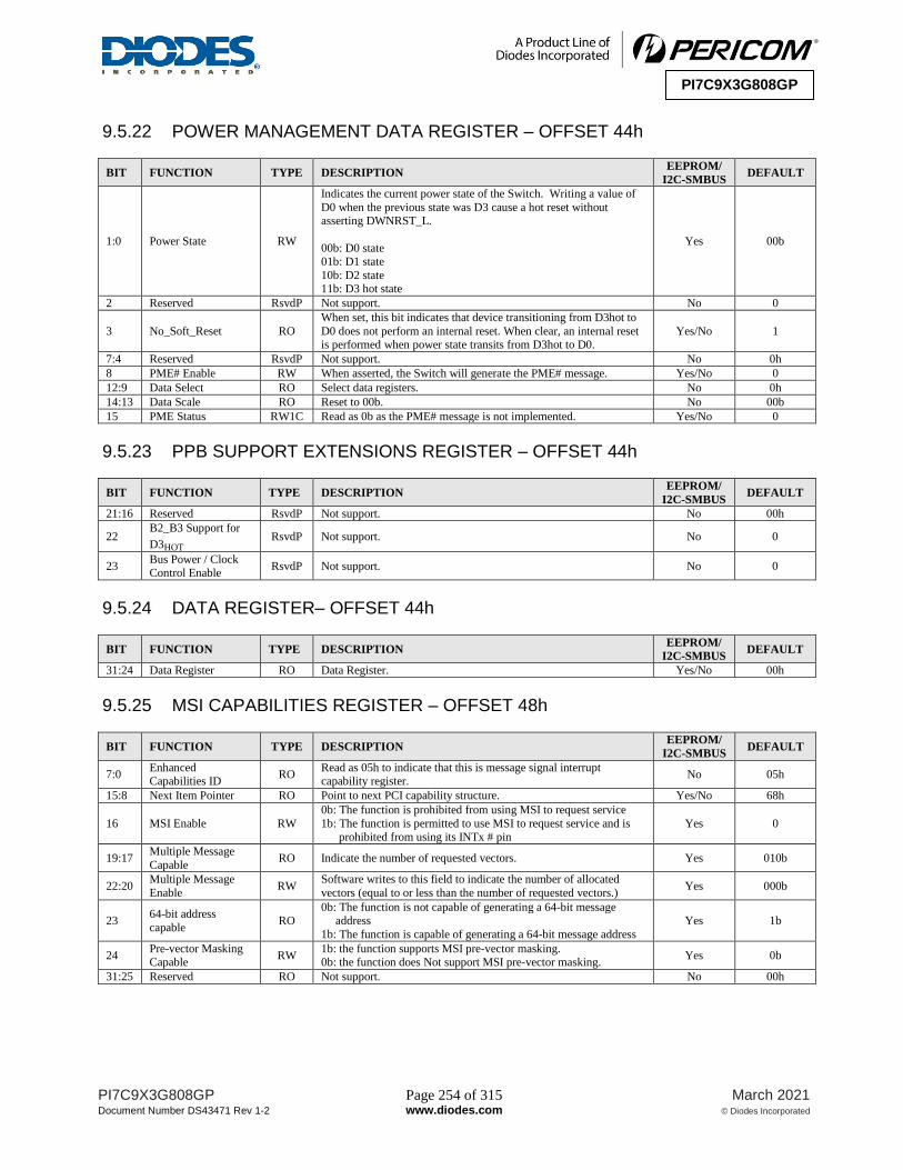
PI7C9X3G808GP Page 254 of 315 March 2021
Document Number DS43471 Rev 1-2 www.diodes.com © Diodes Incorporated
PI7C9X3G808GP
9.5.22 POWER MANAGEMENT DATA REGISTER – OFFSET 44h
BIT FUNCTION TYPE DESCRIPTION EEPROM/
I2C-SMBUS DEFAULT
1:0 Power State RW
Indicates the current power state of the Switch. Writing a value of
D0 when the previous state was D3 cause a hot reset without asserting DWNRST_L.
00b: D0 state 01b: D1 state
10b: D2 state 11b: D3 hot state
Yes 00b
2 Reserved RsvdP Not support. No 0
3 No_Soft_Reset RO
When set, this bit indicates that device transitioning from D3hot to
D0 does not perform an internal reset. When clear, an internal reset is performed when power state transits from D3hot to D0.
Yes/No 1
7:4 Reserved RsvdP Not support. No 0h
8 PME# Enable RW When asserted, the Switch will generate the PME# message. Yes/No 0
12:9 Data Select RO Select data registers. No 0h
14:13 Data Scale RO Reset to 00b. No 00b
15 PME Status RW1C Read as 0b as the PME# message is not implemented. Yes/No 0
9.5.23 PPB SUPPORT EXTENSIONS REGISTER – OFFSET 44h
BIT FUNCTION TYPE DESCRIPTION EEPROM/
I2C-SMBUS DEFAULT
21:16 Reserved RsvdP Not support. No 00h
22 B2_B3 Support for
D3HOT RsvdP Not support. No 0
23 Bus Power / Clock Control Enable
RsvdP Not support. No 0
9.5.24 DATA REGISTER– OFFSET 44h
BIT FUNCTION TYPE DESCRIPTION EEPROM/
I2C-SMBUS DEFAULT
31:24 Data Register RO Data Register. Yes/No 00h
9.5.25 MSI CAPABILITIES REGISTER – OFFSET 48h
BIT FUNCTION TYPE DESCRIPTION EEPROM/
I2C-SMBUS DEFAULT
7:0 Enhanced Capabilities ID
RO Read as 05h to indicate that this is message signal interrupt capability register.
No 05h
15:8 Next Item Pointer RO Point to next PCI capability structure. Yes/No 68h
16 MSI Enable RW
0b: The function is prohibited from using MSI to request service
1b: The function is permitted to use MSI to request service and is prohibited from using its INTx # pin
Yes 0
19:17 Multiple Message
Capable RO Indicate the number of requested vectors. Yes 010b
22:20 Multiple Message
Enable RW
Software writes to this field to indicate the number of allocated
vectors (equal to or less than the number of requested vectors.) Yes 000b
23 64-bit address
capable RO
0b: The function is not capable of generating a 64-bit message address
1b: The function is capable of generating a 64-bit message address
Yes 1b
24 Pre-vector Masking Capable
RW 1b: the function supports MSI pre-vector masking. 0b: the function does Not support MSI pre-vector masking.
Yes 0b
31:25 Reserved RO Not support. No 00h

PI7C9X3G808GP Page 255 of 315 March 2021
Document Number DS43471 Rev 1-2 www.diodes.com © Diodes Incorporated
PI7C9X3G808GP
9.5.26 MESSAGE ADDRESS REGISTER – OFFSET 4Ch
BIT FUNCTION TYPE DESCRIPTION EEPROM/
I2C-SMBUS DEFAULT
1:0 Reserved RsvdP Not support. No 00b
31:2 Message Address RW If the message enable bit is set, the contents of this register specify
the DWORD aligned address for MSI memory write transaction. Yes 0-0h
9.5.27 MESSAGE UPPER ADDRESS REGISTER – OFFSET 50h
BIT FUNCTION TYPE DESCRIPTION EEPROM/
I2C-SMBUS DEFAULT
31:0 Message Upper
Address RW
This register is only effective if the device supports a 64-bit
message address is set. Yes 0000_0000h
9.5.28 MESSAGE DATA REGISTER – OFFSET 54h
BIT FUNCTION TYPE DESCRIPTION EEPROM/
I2C-SMBUS DEFAULT
15:0 Message Data RW Reset to 0. Yes 0000h
9.5.29 MESSAGE MASK REGISTER – OFFSET 58h
BIT FUNCTION TYPE DESCRIPTION EEPROM/
I2C-SMBUS DEFAULT
0 MSI Mask for Hot Plug
RW MSI mask for Hot Plug interrupts. Yes 0
1 MSI Mask for DPC RW MSI mask for DPC interrupts. Yes 0
2 MSI Mask for DMA and GPIO
RW MSI mask for DMAGPIO interrupts. Yes 0
3 MSI Mask for CDEP RW MSI mask for CDEP interrupts. Yes 0
31:4 Reserved RsvdP Not support. No 0000_000h
9.5.30 MESSAGE PENDING REGISTER – OFFSET 5Ch
BIT FUNCTION TYPE DESCRIPTION EEPROM/
I2C-SMBUS DEFAULT
0 MSI Pending for Hot Plug Interrupts
RO MSI pending status for Hot Plug interrupts. No 0
1 MSI Pending for
DPC Interrupts RO MSI pending status for DPC interrupts. No 0
2 MSI Pending for
GPIO Interrupts RO MSI pending status for GPIO interrupts. No 0
3 MSI Pending for CDEP Interrupts
RO MSI pending status for CDEP interrupts. No 0
31:4 Reserved RsvdP Not support. No 0000_000h
9.5.31 PCI EXPRESS CAPABILITIES REGISTER – OFFSET 68h
BIT FUNCTION TYPE DESCRIPTION EEPROM/
I2C-SMBUS DEFAULT
7:0 Enhanced
Capabilities ID RO Read as 10h to indicate that this is PCI express capability register. No 10h
15:8 Next Item Pointer RO Point to next PCI capability structure. Yes/No A4h
19:16 Capability Version RO Read as 2h to indicate the device is compliant to Revision .2.0 of
PCI Express Base Specifications. Yes/No 2h
23:20 Device/Port Type RO Indicates the type of PCI Express logical device. Yes/No 0h
24 Slot Implemented RO
When set, indicates that the PCIe Link associated with this Port is
connected to a slot. This field is valid for downstream ports of the Switch.
Yes/No 0

PI7C9X3G808GP Page 256 of 315 March 2021
Document Number DS43471 Rev 1-2 www.diodes.com © Diodes Incorporated
PI7C9X3G808GP
BIT FUNCTION TYPE DESCRIPTION EEPROM/
I2C-SMBUS DEFAULT
29:25 Interrupt Message Number
RO Read as 0. No MSI messages are generated in the transparent mode. No 00_000b
31:30 Reserved RsvdP Not support. No 00b
9.5.32 DEVICE CAPABILITIES REGISTER – OFFSET 6Ch
BIT FUNCTION TYPE DESCRIPTION EEPROM/
I2C-SMBUS DEFAULT
2:0 Max_Payload_Size Supported
RO Indicates the maximum payload size that the device can support for TLPs. Each port of the Switch supports 512 bytes max payload size.
Yes/No 010b
4:3 Phantom Functions
Supported RO
Indicates the support for use of unclaimed function numbers as
Phantom functions. Read as 00b, since the Switch does not act as a requester.
No 00b
5 Extended Tag Field
Supported RO
Indicates the maximum supported size of Tag field as a Requester.
Read as 0, since the Switch does not act as a requester. No 1
8:6 Endpoint L0s Acceptable Latency
RO
Acceptable total latency that an Endpoint can withstand due to the
transition from L0s state to the L0 state. For Switch, the ASPM
software would not check this value.
No 111b
11:9 Endpoint L1 Acceptable Latency
RO
Acceptable total latency that an Endpoint can withstand due to the
transition from L1 state to the L0 state. For Switch, the ASPM
software would not check this value.
No 111b
14:12 Reserved RsvdP Not support. No 000b
15 Role_Based Error
Reporting RO
When set, indicates that the device implements the functionality
originally defined in the Error Reporting ECN. Yes/No 1
17:16 Reserved RsvdP Not support. No 00b
25:18 Captured Slot Power
Limit Value RO
In combination with the Slot Power Limit Scale value, specifies the
upper limit on power supplied by slot.
This value is set by the Set_Slot_Power_Limit message or
hardwired to 00h.
No 00h
27:26 Captured Slot Power
Limit Scale RO
Specifies the scale used for the Slot Power Limit Value.
This value is set by the Set_Slot_Power_Limit message or hardwired to 00b.
No 00b
31:28 Reserved RsvdP Not support. No 0h
9.5.33 DEVICE CONTROL REGISTER – OFFSET 70h
BIT FUNCTION TYPE DESCRIPTION EEPROM/
I2C-SMBUS DEFAULT
0 Correctable Error Reporting Enable
RW 0b: Disable Correctable Error Reporting 1b: Enable Correctable Error Reporting
Yes 0
1 Non-Fatal Error
Reporting Enable RW
0b: Disable Non-Fatal Error Reporting
1b: Enable Non-Fatal Error Reporting Yes 0
2 Fatal Error Reporting Enable
RW 0b: Disable Fatal Error Reporting 1b: Enable Fatal Error Reporting
Yes 0
3 Unsupported Request
Reporting Enable RW
0b: Disable Unsupported Request Reporting
1b: Enable Unsupported Request Reporting Yes 0
4 Enable Relaxed Ordering
RO
When set, it permits the device to set the Relaxed Ordering bit in
the attribute field of transaction. Since the Switch can not either act as a requester or alter the content of packet it forwards, this bit
always returns ‘0’ when read.
No 0
7:5 Max_Payload_Size RW
This field sets maximum TLP payload size for the device. Permissible values that can be programmed are indicated by the
Max_Payload_Size Supported in the Device Capabilities register.
Any value exceeding the Max_Payload_Size Supported written to this register results into clamping to the Max_Payload_Size
Supported value.
Yes 000b
8 Extended Tag Field
Enable RW
When set, this bit enables a function to ues an 8-bit Tag field as a requester. If the bit is clear, the function is restricted to a 5-bit Tag
field.
Yes 0
9 Reserved RsvdP Not support. No 0

PI7C9X3G808GP Page 257 of 315 March 2021
Document Number DS43471 Rev 1-2 www.diodes.com © Diodes Incorporated
PI7C9X3G808GP
BIT FUNCTION TYPE DESCRIPTION EEPROM/
I2C-SMBUS DEFAULT
10 Auxiliary (AUX) Power PM Enable
RO When set, indicates that a device is enabled to draw AUX power independent of PME AUX power.
No 0
11 Enable No Snoop RO
When set, it permits to set the No Snoop bit in the attribute field of
transaction. Since the Switch can not either act as a requester or alter the content of packet it forwards, this bit always returns ‘0’
when read.
No 0
14:12 Max_Read_ Request_Size
RO
This field sets the maximum Read Request size for the device as a
Requester. Since the Switch does not generate read request by itself,
these bits are hardwired to 0.
No 000b
15 Reserved RsvdP Not support. No 0
9.5.34 DEVICE STATUS REGISTER – OFFSET 70h
BIT FUNCTION TYPE DESCRIPTION EEPROM/
I2C-SMBUS DEFAULT
16 Correctable Error Detected
RW1C
Asserted when correctable error is detected. Errors are logged in
this register regardless of whether error reporting is enabled or not in the Device Control register.
Yes 0
17 Non-Fatal Error Detected
RW1C
Asserted when non-fatal error is detected. Errors are logged in this
register regardless of whether error reporting is enabled or not in the Device Control register.
Yes 0
18 Fatal Error Detected RW1C
Asserted when fatal error is detected. Errors are logged in this
register regardless of whether error reporting is enabled or not in the Device Control register.
Yes 0
19 Unsupported Request
Detected RW1C
Asserted when unsupported request is detected. Errors are logged in
this register regardless of whether error reporting is enabled or not in the Device Control register.
Yes 0
20 AUX Power
Detected RO Asserted when the AUX power is detected by the Switch No 0
21 Transactions Pending RO Each port of Switch does not issue Non-posted Requests on its own
behalf, so this bit is hardwired to 0b. No 0
31:22 Reserved RsvdP Not support. No 0-0h
9.5.35 LINK CAPABILITIES REGISTER – OFFSET 74h
BIT FUNCTION TYPE DESCRIPTION EEPROM/
I2C-SMBUS DEFAULT
3:0 Maximum Link
Speed RO
Indicates the maximum speed of the Express link is 8Gb/s, 5Gb/s and 2.5 Gb/s.
0001b: 2.5 Gb/s
0010b: 5.0 Gb/s
0011b: 8.0 Gb/s Others: Reserved
Yes/No 2h
9:4 Maximum Link Width
RO
Indicates the maximum width of the given PCIe Link. Valid widths
are x1, x2 or x4 which are set by PORTCFG[2:0] strap pins. Please refer to Table 5-1 Mode Selection
00_0001b: x1 lane width
00_0010b: x2 lane width
00_0100b: x4 lane width
Yes
Set by
PORTCFG [2:0]
11:10
Active State Power
Management
(ASPM) Support
RO Indicates the level of ASPM supported on the given PCIe Link. Each port of Switch supports L0s and L1 entry.
Yes/No 10b
14:12 L0s Exit Latency RO
Indicates the L0s exit latency for the given PCIe Link.
The length of time this port requires to complete transition from L0s
to L0 is in the range of 256ns to less than 512ns.
Yes/No 011b
17:15 L1 Exit Latency
RO
Indicates the L1 exit latency for the given PCIe Link.
The length of time this port requires to complete transition from L1
to L0 is less than 1us.
Yes/No 000b
18 Clock Power
Management RsvdP Not support. No 0
19 Surprise Down Capability Enable
RsvdP Not support. No 0

PI7C9X3G808GP Page 258 of 315 March 2021
Document Number DS43471 Rev 1-2 www.diodes.com © Diodes Incorporated
PI7C9X3G808GP
BIT FUNCTION TYPE DESCRIPTION EEPROM/
I2C-SMBUS DEFAULT
20 Data Link Layer Active Reporting
Capable
RsvdP Not support. No 0
21 Link BW Notify Cap.
RsvdP Not support. No 0
22 ASPM Optionality Compliance
RsvdP Not support. No 0
23 Reserved RsvdP Not support. No 0
31:24 Port Number RO Indicates the PCIe Port Number for the given PCIe Link. Yes/No 80h
9.5.36 LINK CONTROL REGISTER – OFFSET 78h
BIT FUNCTION TYPE DESCRIPTION EEPROM/
I2C-SMBUS DEFAULT
1:0
Active State Power
Management (ASPM) Control
RW
00b: ASPM is Disabled 01b: L0s Entry Enabled
10b: L1 Entry Enabled
11b: L0s and L1 Entry Enabled
Note that the receiver must be capable of entering L0s even when the field is disabled
Yes 00b
2 Reserved RsvdP Not support. No 0
3 Read Completion
Boundary (RCB) RsvdP Not support. No 0
4 Link Disable RsvdP Not support. No 0
5 Retrain Link RsvdP Not support. No 0
6 Common Clock
Configuration RW
0b: The components at both ends of a link are operating with
synchronous reference clock
1b: The components at both ends of a link are operating with a
distributed common reference clock
Yes 0
7 Extended Synch RW
When set, it transmits 4096 FTS ordered sets in the L0s state for
entering L0 state and transmits 1024 TS1 ordered sets in the L1
state for entering L0 state.
Yes 0
8 Enable Clock Power
Management RsvdP Not support. No 0
9 HW Autonomous Width Disable
RsvdP Not support. No 0
10
Link Bandwidth
Management Interrupt Enable
RsvdP Not support. No 0
11
Link Autonomous
Bandwidth Interrupt Enable
RsvdP Not support. No 0
15:12 Reserved RsvdP Not support. No 0h
9.5.37 LINK STATUS REGISTER – OFFSET 78h
BIT FUNCTION TYPE DESCRIPTION EEPROM/
I2C-SMBUS DEFAULT
19:16 Link Speed RO
Indicate the negotiated speed of the Express link.
0001b: 2.5 Gb/s
0010b: 5.0 Gb/s 0011b: 8.0 Gb/s
No 0h
25:20 Negotiated Link
Width RO
Indicates the negotiated width of the given PCIe link.
00_0001b: x1 lane width
00_0010b: x2 lane width 00_0100b: x4 lane width
No Set by
PORTCFG
[2:0]
26 Training Error RO
When set, indicates a Link training error occurred.
This bit is cleared by hardware upon successful training of the link to the L0 link state.
No 0

PI7C9X3G808GP Page 259 of 315 March 2021
Document Number DS43471 Rev 1-2 www.diodes.com © Diodes Incorporated
PI7C9X3G808GP
BIT FUNCTION TYPE DESCRIPTION EEPROM/
I2C-SMBUS DEFAULT
27 Link Training RO When set, indicates the link training is in progress. Hardware clears this bit once link training is complete.
No 0
28 Slot Clock Configuration
RO
0b: the Switch uses an independent clock irrespective of the
presence of a reference on the connector 1b: the Switch uses the same reference clock that the platform
provides on the connector
Yes/No 0
29 Data Link Layer
Link Active RO
Indicates the status of the Data Link Control and Management State
Machine.
1b: indicate the DL_Active state
0b: otherwise
No 0
30 Link Bandwidth
Management Status RsvdP Not support. No 0
31 Link Autonomous
Bandwidth Status RsvdP Not support. No 0
9.5.38 SLOT CAPABILITIES REGISTER – OFFSET 7Ch
BIT FUNCTION TYPE DESCRIPTION EEPROM/
I2C-SMBUS DEFAULT
31:0 Reserved RsvdP Not support. No 0000_0000h
9.5.39 SLOT CONTROL REGISTER – OFFSET 80h
BIT FUNCTION TYPE DESCRIPTION EEPROM/
I2C-SMBUS DEFAULT
15:0 Reserved RsvdP Not support. No 0000h
9.5.40 SLOT STATUS REGISTER – OFFSET 80h
BIT FUNCTION TYPE DESCRIPTION EEPROM/
I2C-SMBUS DEFAULT
31:16 Reserved RsvdP Not support. No 0-0h
9.5.41 DEVICE CAPABILITIES REGISTER 2 – OFFSET 8Ch
BIT FUNCTION TYPE DESCRIPTION EEPROM/
I2C-SMBUS DEFAULT
31:0 Reserved RsvdP Not support. No 0000_0000h
9.5.42 DEVICE CONTROL REGISTER 2 – OFFSET 90h
BIT FUNCTION TYPE DESCRIPTION EEPROM/
I2C-SMBUS DEFAULT
15:0 Reserved RsvdP Not support. No 0000h
9.5.43 DEVICE STATUS REGISTER 2 – OFFSET 90h
BIT FUNCTION TYPE DESCRIPTION EEPROM/
I2C-SMBUS DEFAULT
31:16 Reserved RsvdP Not support. No 0000h
9.5.44 LINK CAPABILITIES REGISTER 2 – OFFSET 94h
BIT FUNCTION TYPE DESCRIPTION EEPROM/
I2C-SMBUS DEFAULT
0 Reserved RsvdP Not support. No 0

PI7C9X3G808GP Page 260 of 315 March 2021
Document Number DS43471 Rev 1-2 www.diodes.com © Diodes Incorporated
PI7C9X3G808GP
BIT FUNCTION TYPE DESCRIPTION EEPROM/
I2C-SMBUS DEFAULT
7:1 Supported Link Speeds Vector
RO
This field indicates the supported Link speed of the associated Port.
bit[0]… 2.5 GT/s bit[1]… 5.0 GT/s
bit[2]… 8.0 GT/s
bit[6:3]… RsvdP
No 0-0b
8 Crosslink Supported RO 0b: Crosslink is Not supported
1b: Crosslink is supported No 0
31:9 Reserved RsvdP Not support. No 0-0b
9.5.45 LINK CONTROL REGISTER 2 – OFFSET 98h
BIT FUNCTION TYPE DESCRIPTION EEPROM/
I2C-SMBUS DEFAULT
3:0 Target Link Speed RW
0001b: 2.5GT/s link speed is supported
0010b: 5.0GT/s link speed is supported
0011b: 8.0GT/s link speed is supported Others: reserved.
Yes 2h
4 Enter Compliance RW 1b: enter compliance Yes 0
5 HW_AutoSpeed_Dis RW When set, this bit disables hardware from changing the link speed for device-specific reasons other than attempting to correct
unreliable link operation by reducing link speed.
Yes 0
6 Select_Deemp RO
Valid for downstream ports only.
0b: Select -3.5db de-emphasis
1b: Select -6.0 db de-emphasis
Yes/No 0
9:7 Tran_Margin RW This field controls the value of the non-deemphasized voltage level
at the transmitter pins. Yes 000b
10 Enter Modify
Compliance RW
Valid for upstream port only.
When set, the device transmits modified compliance pattern if the
LTSSM enters Polling.Compliance substate.
Yes 0
11 Compliance SOS RW
Valid for upstream port only.
When set, the LTSSM is required to send SKP Ordered Sets between sequences when sending the Compliance Pattern or
Modified Compliance Pattern.
Yes 0
15:12 Compliance
Preset/De-emphasis RW This field is intended for debug and compliance testing purpose. Yes 000b
9.5.46 LINK STATUS REGISTER 2 – OFFSET 98h
BIT FUNCTION TYPE DESCRIPTION EEPROM/
I2C-SMBUS DEFAULT
16 Current De-emphasis level
RO 1b: -3.5dB 0b: -6 dB
No 1
17 Equalization
Complete RO
When set to 1b, this bit indicates that the Transmitter Equalization
procedure has completed. No 0
18 Equalization Phase 1 Successful
RO When set to 1b, this bit indicates that Phase 1 of Transmitter Equalization procedure has successfully completed.
No 0
19 Equalization Phase 2
Successful RO
When set to 1b, this bit indicates that Phase 2 of Transmitter
Equalization procedure has successfully completed. No 0
20 Equalization Phase 3
Successful RO
When set to 1b, this bit indicates that Phase 3 of Transmitter
Equalization procedure has successfully completed. No 0
21 Link Equalization Request
RW1C This bit is set by hardware to request the Link equalization process to be performed on the link.
Yes 0
27:22 Reserved RsvdP Not support. No 0-0b
30:28 Downstream
Component Presence RO
This field indicates the presence and DRS status for the Downstream Component.
000b: Link Down – Presence Not Determined 001b: Link Down – Component Not Present
010b: Link Down – Component Present 011b: Reserved
No 000b

PI7C9X3G808GP Page 261 of 315 March 2021
Document Number DS43471 Rev 1-2 www.diodes.com © Diodes Incorporated
PI7C9X3G808GP
BIT FUNCTION TYPE DESCRIPTION EEPROM/
I2C-SMBUS DEFAULT
100b: Link Up – Component Present 101b: Link Up – Component Present and DRS Received
110b: Reserved 111b: Reserved
31 DRS Message
Received RW1C This bit must be set whenever the Port receives a DRS message. Yes 0
9.5.47 SLOT CAPABILITIES REGISTER 2 – OFFSET 9Ch
BIT FUNCTION TYPE DESCRIPTION EEPROM/
I2C-SMBUS DEFAULT
31:0 Reserved RsvdP Not support. No 0000_0000h
9.5.48 SLOT CONTROL REGISTER 2 – OFFSET A0h
BIT FUNCTION TYPE DESCRIPTION EEPROM/
I2C-SMBUS DEFAULT
15:0 Reserved RsvdP Not support. No 0000_0000h
9.5.49 SLOT STATUS REGISTER 2 – OFFSET A0h
BIT FUNCTION TYPE DESCRIPTION EEPROM/
I2C-SMBUS DEFAULT
31:16 Reserved RsvdP Not support. No 0000_0000h
9.5.50 SSID/SSVID CAPATILITIES REGISTER – OFFSET A4h
BIT FUNCTION TYPE DESCRIPTION EEPROM/
I2C-SMBUS DEFAULT
7:0 SSID/SSVID
Capabilities ID RO Read as 0Dh to indicate that this is SSID/SSVID capability register. Yes/No 0Dh
15:8 Next Item Pointer RO Point to next PCI capability structure. Yes/No B0h
31:16 Reserved RsvdP Not support. No 0000h
9.5.51 SUBSYSTEM VENDOR ID REGISTER – OFFSET A8h
BIT FUNCTION TYPE DESCRIPTION EEPROM/
I2C-SMBUS DEFAULT
15:0 SSVID RO It indicates the sub-system vendor id. Yes 12D8h
9.5.52 SUBSYSTEM ID REGISTER – OFFSET A8h
BIT FUNCTION TYPE DESCRIPTION EEPROM/
I2C-SMBUS DEFAULT
31:16 SSID RO It indicates the sub-system device id. Yes C008h
9.5.53 MSI-X CAPATILITIES REGISTER – OFFSET B0h
BIT FUNCTION TYPE DESCRIPTION EEPROM/
I2C-SMBUS DEFAULT
7:0 MSI-X Capabilities
ID RO Read as 11h to indicate that this is MSI-X capability register. No 11h
15:8 Next Item Pointer RO Indicates next capability pointer. Yes C8h
26:16 Table Size RO System software reads this field to determine the MSI-X Table Size N, which is encoded as N-1.
No 000h
29:27 Reserved RsvdP Not support, No 000b

PI7C9X3G808GP Page 262 of 315 March 2021
Document Number DS43471 Rev 1-2 www.diodes.com © Diodes Incorporated
PI7C9X3G808GP
BIT FUNCTION TYPE DESCRIPTION EEPROM/
I2C-SMBUS DEFAULT
30 Function Mask RW
If set, all of the vectors associated with the function are masked, regardless of their per-vector mask bit values.
If clear, each vector’s mask bit determines whether the vector is masked or not.
Yes 0
31 MSI-X Enable RW
If set and the MSI Enable bit in the MSI Message Control register is
clear, the function is permitted to use MSI-X to request service and is prohibited from using INTx interrupts (if implemented).
If clear, the function is prohibited from using MSI-X to request
service.
Yes 0
9.5.54 MSI-X TABLE OFFSET / TABLE BIR REGSITER – OFFSET B4h
BIT FUNCTION TYPE DESCRIPTION EEPROM/
I2C-SMBUS DEFAULT
2:0 Table BIR RO
Read as 000b to indicate Base Address 0 register (offset 10h in
Configuration Space) is used to map the function MSI-X Table into
Memory space.
Yes 000b
31:3 Table Offset RO
Used as an offset from the address contained by one of the
function’s Base Address registers to point to the base of the MSI-X Table.
Yes 0000_FE00h
9.5.55 MSI-X PBA OFFSET / PBA BIR REGISTER – OFFSET B8h
BIT FUNCTION TYPE DESCRIPTION EEPROM/
I2C-SMBUS DEFAULT
2:0 PBA BIR RO
Read as 000b to indicate Base Address 0 register (offset 10h in
Configuration Space) is used to map the function MSI-X PBA into Memory space.
Yes 000b
31:3 PBA Offset RO
Used as an offset from the address contained by one of the
function’s Base Address registers to point to the base of the MSI-X PBA.
Yes 0000_FE10h
9.5.56 VENDOR SPECIFIC CAPABILITY REGISTER – OFFSET C8h
BIT FUNCTION TYPE DESCRIPTION EEPROM/
I2C-SMBUS DEFAULT
7:0 Enhanced
Capabilities ID RO
Read as 09h to indicate that these are vendor specific capability
registers. No 09h
15:8 Next Item Pointer RO Read as 00h. No other ECP registers. No 00h
31:16 Length Information RO The length field provides the information for number of bytes in the
capability structure. No 0038h
9.5.57 BAR 0-1 CONFIGURATION REGISTER – OFFSET E4h
BIT FUNCTION TYPE DESCRIPTION EEPROM/
I2C-SMBUS DEFAULT
1:0 BAR 0 Type RW
00b: disable 01b: reserved
10b: BAR0 is implemented as a 32-bit Memory BAR.
11b: BAR0/1 is implemented as a 64-bit Memory BAR.
Yes 10b
2 BAR0 Prefetch RW 0b: Non-Prefetchable
1b: Prefetchable Yes 0b
31:3 Reserved RsvdP Not support. No 0000_0000h
9.5.58 BAR 2 CONFIGURATION REGISTER – OFFSET E8h
BIT FUNCTION TYPE DESCRIPTION EEPROM/
I2C-SMBUS DEFAULT
0 Type Selector RsvdP Not supported. No 0
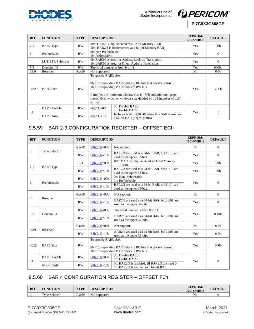
PI7C9X3G808GP Page 263 of 315 March 2021
Document Number DS43471 Rev 1-2 www.diodes.com © Diodes Incorporated
PI7C9X3G808GP
BIT FUNCTION TYPE DESCRIPTION EEPROM/
I2C-SMBUS DEFAULT
2:1 BAR2 Type RW 00b: BAR2 is implemented as a 32 bit Memory BAR 10b: BAR2/3 is implemented as a 64-bit Memory BAR
Yes 00b
3 Prefetchable RW 0b: Non Prefetchable
1b: Prefetchable Yes 0
4 LUT/BTR Selection RW 0b: BAR2/3 is used for Address Look-up Translation.
1b: BAR2/3 is used for Direct Address Translation. Yes 0
8:5 Domain ID RW The valid number is from 0 to 11. Yes 0000b
19:9 Reserved RsvdP Not supported. No 0-0b
30:20 BAR2 Size RW
To specify BAR2 size.
0b: Corresponding BAR2 bits are RO bits that always return 0
1b: Corresponding BAR2 bits are RW bits
It implies the minimum window size is 1MB and minimum page
size is 8KB, which is windows size divided by 128 (number of LUT entries).
Yes 7FFh
31
BAR 2 Enable RW bit[2:1]=00b 0b: Disable BAR2
1b: Enable BAR2 Yes 1
BAR 2 Size RW bit[2:1]=10b Includes with bit[30:20] when this BAR is used as a 64-bit BAR (bit[2:1]=10b).
9.5.59 BAR 2-3 CONFIGURATION REGISTER – OFFSET ECh
BIT FUNCTION TYPE DESCRIPTION EEPROM/
I2C-SMBUS DEFAULT
0 Type Selector
RsvdP E8h[2:1]=00b Not support. No 0
RW E8h[2:1]=10b BAR2/3 are used as a 64-bit BAR, bit[31:0] are
used as the upper 32-bits. Yes 0
2:1 BAR3 Type
RO E8h[2:1]=00b 00b: BAR3 is implemented as 32 bit Memory
BAR. Yes 00b
RW E8h[2:1]=10b BAR2/3 are used as a 64-bit BAR, bit[31:0] are
used as the upper 32-bits. Yes 00b
3 Prefetchable
RW E8h[2:1]=00b 0b: Non Prefetchable
1b: Prefetchable Yes 0
RW E8h[2:1]=10b BAR2/3 are used as a 64-bit BAR, bit[31:0] are
used as the upper 32-bits.
4 Reserved
RsvdP E8h[2:1]=00b Not support. No 0
RW E8h[2:1]=10b BAR2/3 are used as a 64-bit BAR, bit[31:0] are
used as the upper 32-bits. Yes 0
8:5 Domain ID
RW E8h[2:1]=00b The valid number is from 0 to 11.
Yes 0000b
RW E8h[2:1]=10b BAR2/3 are used as a 64-bit BAR, bit[31:0] are
used as the upper 32-bits.
19:9 Reserved
RsvdP E8h[2:1]=00b Not support. No 0-0b
RW E8h[2:1]=10b BAR2/3 are used as a 64-bit BAR, bit[31:0] are
used as the upper 32-bits. Yes 0-0b
30:20 BAR3 Size RW
To specify BAR3 size.
0b: Corresponding BAR3 bits are RO bits that always return 0
1b: Corresponding BAR3 bits are RW bits
Yes 000h
31
BAR 3 Enable RW E8h[2:1]=00b 0b: Disable BAR3
1b: Enable BAR3 Yes 0
64-Bit BAR RW E8h[2:1]=10b 0b: BAR2/3 is disabled, all BAR2/3 bits read 0. 1b: BAR2/3 is enabled as a 64-bit BAR.
9.5.60 BAR 4 CONFIGURATION REGISTER – OFFSET F0h
BIT FUNCTION TYPE DESCRIPTION EEPROM/
I2C-SMBUS DEFAULT
0 Type Selector RsvdP Not supported. No 0

PI7C9X3G808GP Page 264 of 315 March 2021
Document Number DS43471 Rev 1-2 www.diodes.com © Diodes Incorporated
PI7C9X3G808GP
BIT FUNCTION TYPE DESCRIPTION EEPROM/
I2C-SMBUS DEFAULT
2:1 BAR4 Type RW 00b: BAR4 is implemented as a 32 bit Memory BAR 10b: BAR4/5 is implemented as a 64-bit Memory BAR
Yes 00b
3 Prefetchable RW 0b: Non Prefetchable
1b: Prefetchable Yes 0
4 LUT/BTR Selection RW 0b: BAR4/5 is used for Address Look-up Translation.
1b: BAR4/5 is used for Direct Address Translation. Yes 0
8:5 Domain ID RW The valid number is from 0 to 11. Yes 0000b
19:9 Reserved RsvdP Not supported. No 0-0b
30:20 BAR 4 Size RW
To specify BAR4 size.
0b: Corresponding BAR4 bits are RO bits that always return 0
1b: Corresponding BAR4 bits are RW bits
Yes 7FFh
31
BAR 4 Enable RW bit[2:1]=00b 0b: Disable BAR4 1b: Enable BAR4
Yes 1
BAR 4 Size RW bit[2:1]=10b Includes with bit[30:20] when this BAR is used as
a 64-bit BAR (bit[2:1]=10b).
9.5.61 BAR 4-5 CONFIGURATION REGISTER – OFFSET F4h
BIT FUNCTION TYPE DESCRIPTION EEPROM/
I2C-SMBUS DEFAULT
0 Type Selector
RsvdP F0h[2:1]=00b Not support. No 0
RW F0h[2:1]=10b BAR4/5 are used as a 64-bit BAR, bit[31:0]are
used as the upper 32-bits. Yes 0
2:1 BAR 5 Type
RO F0h[2:1]=00b 00b: BAR5 is implemented as 32 bit Memory
BAR. Yes 00b
RW F0h[2:1]=10b BAR4/5 are used as a 64-bit BAR, bit[31:0]are used as the upper 32-bits.
Yes 00b
3 Prefetchable
RW F0h[2:1]=00b 0b: Non Prefetchable
1b: Prefetchable Yes 0
RW F0h[2:1]=10b BAR4/5 are used as a 64-bit BAR, bit[31:0]are used as the upper 32-bits.
4 Reserved
RsvdP F0h[2:1]=00b Not support. No 0
RW F0h[2:1]=10b BAR4/5 are used as a 64-bit BAR, bit[31:0]are used as the upper 32-bits.
Yes 0
8:5 Domain ID
RW F0h[2:1]=00b The valid number is from 0 to 11.
Yes 0000b
RW F0h[2:1]=10b BAR4/5 are used as a 64-bit BAR, bit[31:0]are used as the upper 32-bits.
19:9 Reserved
RsvdP F0h[2:1]=00b Not support. No 0-0b
RW F0h[2:1]=10b BAR4/5 are used as a 64-bit BAR, bit[31:0]are used as the upper 32-bits.
Yes 0-0b
30:20 BAR 5 Size RW
To specify BAR5 size.
0b: Corresponding BAR 5 bits are RO bits that always return 0
1b: Corresponding BAR5 bits are RW bits
Yes 000h
31
BAR 5 Enable RW F0h[2:1]=00b 0b: Disable BAR5 1b: Enable BAR5
Yes 0
64-Bit BAR RW F0h[2:1]=10b 0b: BAR4/5 is disabled, all BAR4/5 bits read 0.
1b: BAR4/5 is enabled as a 64-bit BAR.
9.5.62 DEVICE SERIAL NUMBER ENHANCED CAPABILITY HEADER REGISTER – OFFSET 100h
BIT FUNCTION TYPE DESCRIPTION EEPROM/
I2C-SMBUS DEFAULT
15:0 Extended Capabilities ID
RO Read as 0003h to indicate that this is PCI express extended capability register for device serial number.
No 0003h
19:16 Capability Version RO Must be 1h for this version. No 1h

PI7C9X3G808GP Page 265 of 315 March 2021
Document Number DS43471 Rev 1-2 www.diodes.com © Diodes Incorporated
PI7C9X3G808GP
BIT FUNCTION TYPE DESCRIPTION EEPROM/
I2C-SMBUS DEFAULT
31:20 Next Capability Offset
RO Point to next PCI extended capability structure. Yes/No 900h
9.5.63 DEVICE SERIAL NUMBER LOWER DW REGISTER – OFFSET 104h
BIT FUNCTION TYPE DESCRIPTION EEPROM/
I2C-SMBUS DEFAULT
31:0 Device serial number
1st DW RO Reset to 0000_12D8h. Yes/No 0000_12D8h
9.5.64 DEVICE SERIAL NUMBER HIGHTER DW REGISTER – OFFSET 108h
BIT FUNCTION TYPE DESCRIPTION EEPROM/
I2C-SMBUS DEFAULT
31:0 Device serial number
2nd DW RO Reset to 0816_4896h. Yes/No 0816_4896h
9.5.65 OPERATION MODE REGISTER – OFFSET 348h (Port 0 Only)
BIT FUNCTION TYPE DESCRIPTION EEPROM/
I2C-SMBUS DEFAULT
2:0 Reserved RsvdP Not support. No 000b
5:3 pkgsel RO Package Bonding option. No 000b
8:6 portcfg RO
Port/lane configuration settins. They are decided by the status of
PORTCFG[2:0] strap pins 001b: 2 x4 ports 010b: 1 x4, 2 x2 ports
011b: 4 x2 ports
100b: 1 x4, 4 x1 ports 101b: 8 x1 ports
Others: Reserved
No
Set by
PORTCFG
[2:0]
10:9 chipmode RO
Chip operation mode selection. They are decided by the status of CHIPMODE[1:0] strap pins.
00b: Normal mode
01b: iddq/mbist mode 10b: AC JTAG mode
11b: phy_mode
No 00b
12:11 Reserved RsvdP Not support. No 00b
13 ckmode RO
Reference clock modes. It is decided by the status of CKMODE
strap pin.
0b: base mode
1b: CDEP separate reference mode
No 0b
14 dma_mode RO 0b: disable DMA 1b: enable DMA
No 0
20:15 upport_sel RO Upstream port selection. No 0000_00b
21 CDEP_mode RO 0b: disable CDEP 1b: enable CDEP
No 0
22 scan_tm RO 0b: normal mode
1b: scan mode No 0
23 hotplug_pin_en RO
It is decided by the status of HOT_PLUG_EN_L strap pin.
0b: GPIO[31:0] are GPIO pins 1b: GPIO[31:0] are used as hot plug pins
No 1
24 surprise_hp_en RO
It is decided by the status of SURPRISE_HP strap pin.
0b: disable surprise hot-plug
1b: enable surprise hot-plug
No 0
25 ioe_40bit_en RO 0b: support 16 bit IOE 1b: support 40 bit IOE
No 0

PI7C9X3G808GP Page 266 of 315 March 2021
Document Number DS43471 Rev 1-2 www.diodes.com © Diodes Incorporated
PI7C9X3G808GP
BIT FUNCTION TYPE DESCRIPTION EEPROM/
I2C-SMBUS DEFAULT
26 clkbuf_pd RO
It is decided by the status of CLKBUFPD_L strap pin.
0b: clock buffer is in normal mode 1b: clock buffer is in power down mode
No 1
27 pm_l1_1_en RO
It is decided by the status of PM_L11_EN_L strap pin.
0b: GPIO[15:8] are GPIO pins
1b: GPIO[15:8] are used as CLKREQ_L[7:0]
No Set by
PM_L11_EN_L
30:28 i2c/smaddr_out RO Indicate I2C/SMBUS address. No set by
I2C_ADDRESS
[2:0]
31 Reserved RsvdP Not Support. No 1
9.5.66 TL CSR 0 REGISTER – OFFSET 4C0h
BIT FUNCTION TYPE DESCRIPTION EEPROM/
I2C-SMBUS DEFAULT
7:0 Reserved RsvdP Not support. No 00h
8 p_inta_slot RW Internal used only. Yes 0
9 p_inta_gpio RW Internal used only. Yes 0
10 p_inta_ntl RW Internal used only. Yes 0
31:11 Reserved RsvdP Not support. No 0-0h
9.5.67 VENDOR SPECIFIC CAPABILITIES REGISTER – OFFSET 900h
BIT FUNCTION TYPE DESCRIPTION EEPROM/
I2C-SMBUS DEFAULT
15:0 Extended
Capabilities ID RO
Read as 000Bh to indicate that this is PCI express extended
capability register for vendor specific. No 000Bh
19:16 Capability Version RO Read as 1h. No 1h
31:20 Next Capability
Offset RO Read as 000h. No other ECP registers. No 000h
9.5.68 VENDOR SPECIFIC HEADER REGISTER – OFFSET 904h
BIT FUNCTION TYPE DESCRIPTION EEPROM/
I2C-SMBUS DEFAULT
15:0 VSEC ID RO This field is a vendor-defined ID number that indicates the nature and format of the VSEC structure.
No 0001h
19:16 VSEC Rev RO This field is a vendor-defined version number that indicates the
version of the VSEC structure. No 0h
31:20 VSEC Length RO This field indicates the number of bytes in the entire VSEC structure.
No 280h
9.5.69 BTR 2 REGISTER – OFFSET 908h
BIT FUNCTION TYPE DESCRIPTION EEPROM/
I2C-SMBUS DEFAULT
0 3DW Address Space RW 0b: the translated TLP header is in 4DW format
1b: the translated TLP header is in 3DW format Yes 0
19:1 Reserved RsvdP Not support. No 0_0000h
31:20 Memory BAR 2
Address Translation RW
This is the destination base address for Direct Address Translation.
Valid when BAR 2 is enabled (offset E8h[31]=1).
Please note that the source base address used in DAT is defined in BAR 2 located at offset 18h
Yes 000h

PI7C9X3G808GP Page 267 of 315 March 2021
Document Number DS43471 Rev 1-2 www.diodes.com © Diodes Incorporated
PI7C9X3G808GP
9.5.70 BTR 3 REGISTER – OFFSET 90Ch
BIT FUNCTION TYPE DESCRIPTION EEPROM/
I2C-SMBUS DEFAULT
19:0 Reserved
RsvdP E8h[2:1]=00b Not support No
0_0000h
RW E8h[2:1]=10b BAR2/3 are used as a 64-bit source BAR, the bit[31:0] are used as the upper 32-bits of
destination base address.
Yes
31:20 Memory BAR 3
Address Translation RW
E8h[2:1]=00b Valid when BAR 3 is enabled (offset ECh
[31]=1).
Yes 000h
E8h[2:1]=10b BAR2/3 are used as a 64-bit source BAR, the bit[31:0] are used as the upper 32-bits of
destination base address.
9.5.71 BTR 4 REGISTER – OFFSET 910h
BIT FUNCTION TYPE DESCRIPTION EEPROM/
I2C-SMBUS DEFAULT
0 3DW Address Space RW 0b: the translated TLP header is in 4DW format
1b: the translated TLP header is in 3DW format Yes 0
19:1 Reserved RsvdP Not support. No 0_0000h
31:20 Memory BAR 4
Address Translation RW
This is the destination base address for Direct Address Translation.
Valid when BAR 4 is enabled (offset F0h[31]=1).
Please note that the source base address used in DAT is defined in BAR 4 located at offset 20h
Yes 000h
9.5.72 BTR 5 REGISTER – OFFSET 914h
BIT FUNCTION TYPE DESCRIPTION EEPROM/
I2C-SMBUS DEFAULT
19:0 Reserved
RsvdP F0h[2:1]=00b Not support. No
0_0000h
RW F0h[2:1]=10b
BAR4/5 are used as a 64-bit source BAR, the
bit[31:0] are used as the upper 32-bits of destination base address.
Yes
31:20 Memory BAR 5 Address Translation
RW
F0h[2:1]=00b Valid when BAR 5 is enabled (offset
F4h[31]=1).
Yes 000h
F0h[2:1]=10b BAR4/5 are used as a 64-bit source BAR, the bit[31:0] are used as the upper 32-bits of
destination base address.
9.5.73 ADDRESS LUT ACCESS ADDRESS REGISTER – OFFSET 918h
BIT FUNCTION TYPE DESCRIPTION EEPROM/
I2C-SMBUS DEFAULT
6:0 Index RW Used to indicate the LUT Entry number. Yes 000_0000b
7 Reserved RsvdP Not support. No 0
8 Command WO
0b: Read command
1b: Write command
Return ‘0’ when read always.
Yes 0
31:10 Reserved RsvdP Not support. No 0-0h

PI7C9X3G808GP Page 268 of 315 March 2021
Document Number DS43471 Rev 1-2 www.diodes.com © Diodes Incorporated
PI7C9X3G808GP
9.5.74 ADDRESS LUT ACCESS DATA 0 REGISTER – OFFSET 91Ch
BIT FUNCTION TYPE DESCRIPTION EEPROM/
I2C-SMBUS DEFAULT
0 3DW Address Space RW 0b: the translated TLP header is in 4DW format
1b: the translated TLP header is in 3DW format Yes 0
4:1 Domain Number RW Used to indicate the domain number. Yes 0000b
12:5 Reserved RsvdP Not support. No 0-0b
31:13 LUT Data[31:13] RW Used to indicate LUT Data[31:13]. Yes 0000_0h
9.5.75 ADDRESS LUT ACCESS DATA 1 REGISTER – OFFSET 920h
BIT FUNCTION TYPE DESCRIPTION EEPROM/
I2C-SMBUS DEFAULT
31:0 LUT HData[31:0] RW Used to indicate the higher 32-bit destination base address in 64-bit
address domain. Yes 0000_0000h
9.5.76 ID/DOMAINLUT 0 – 15– OFFSET 924h to 960h
These 16 32-bit registers construct a Requester ID (RID) look-up table storing the RID of TLP issued from Primary
Host, which connected to the upstream port directly. The table content can be either built by hardware automatically or
written by software of management CPU. There are control signals defined in the 14th
and 15th
bits of Device
Configuration 2 Register at offset 50Ch of Port 0 to decide RID LUT build-up mechanism for CDVEP P0 and CDLEP
P4 respectively.
Table 9-10: 16-Bit ID/Domain LUT Entry 0-15 Register Locations CFG_OFFSET ID/DomainLUT Entry_n CFG_OFFSET ID/Domain LUT Entry_n
924h 0 944h 8
928h 1 948h 9
92Ch 2 94Ch 10
930h 3 950h 11
934h 4 954h 12
938h 5 958h 13
93Ch 6 95Ch 14
940h 7 960h 15
Table 9-11: 16-Bit ID/Domain LUT Entry_n (n=0 through 15)
BIT FUNCTION TYPE DESCRIPTION EEPROM/
I2C-SMBUS DEFAULT
15:0 ReqID RW
bit[2:0]: function number
bit[7:3]: device number
bit[15:8]: bus number
Yes 0000h
30:16 Reserved RsvdP Not support. No 0-0b
31 Valid RW 0b: the entry is not valid
1b: the entry is valid Yes 0
9.5.77 CAPTURED BUS ID FOR DOMAIN 0 to 3 – OFFSTE 994h
BIT FUNCTION TYPE DESCRIPTION EEPROM/
I2C-SMBUS DEFAULT
7:0 Dom. 0 Bus Number RW To set the captured bus number for Domain 0 as a destination Bus Number in RID translation.
Yes 00h
15:8 Dom. 1 Bus Number RW To set the captured bus number for Domain 1 as a destination Bus
Number in RID translation. Yes 00h
23:16 Dom. 2 Bus Number RW To set the captured bus number for Domain 2 as a destination Bus
Number in RID translation. Yes 00h
31:24 Dom. 3 Bus Number RW To set the captured bus number for Domain 3 as a destination Bus Number in RID translation
Yes 00h

PI7C9X3G808GP Page 269 of 315 March 2021
Document Number DS43471 Rev 1-2 www.diodes.com © Diodes Incorporated
PI7C9X3G808GP
9.5.78 CAPTURED BUS ID FOR DOMAIN 4 to 7 – OFFSET 998h
BIT FUNCTION TYPE DESCRIPTION EEPROM/
I2C-SMBUS DEFAULT
7:0 Dom. 4 Bus Number RW To set the captured bus number for Domain 4 as a destination Bus
Number in RID translation. Yes 00h
15:8 Dom. 5 Bus Number RW To set the captured bus number for Domain 5 as a destination Bus Number in RID translation.
Yes 00h
23:16 Dom. 6 Bus Number RW To set the captured bus number for Domain 6 as a destination Bus
Number in RID translation. Yes 00h
31:24 Dom. 7 Bus Number RW To set the captured bus number for Domain 7 as a destination Bus
Number in RID translation Yes 00h
9.5.79 CAPTURED BUS ID FORDOMAIN 8 to 11 – OFFSET 99Ch
BIT FUNCTION TYPE DESCRIPTION EEPROM/
I2C-SMBUS DEFAULT
7:0 Dom. 8 Bus Number RW To set the captured bus number for Domain 8 as a destination Bus Number in RID translation.
Yes 00h
15:8 Dom. 9 Bus Number RW To set the captured bus number for Domain 9 as a destination Bus
Number in RID translation. Yes 00h
23:16 Dom. 10 Bus Number
RW To set the captured bus number for Domain 10 as a destination Bus Number in RID translation.
Yes 00h
31:24 Dom. 11 Bus
Number RW
To set the captured bus number for Domain 11 as a destination Bus
Number in RID translation Yes 00h
9.5.80 DOOR BELL IRQ SET REGISTER – OFFSET 9C4h
BIT FUNCTION TYPE DESCRIPTION EEPROM/
I2C-SMBUS DEFAULT
31:0 Set IRQ RW
Set virtual interface IRQ to control the state of the virtual interface
doorbell interrupt request. Reading returns the status of the bits.
Writing 0 to a bit in the register has no effect.
Writing 1 to a bit in the register sets the corresponding interrupt request.
Yes 0000_0000h
9.5.81 DOOR BELL IRQ CLEAR REGISTER – OFFSET 9C8h
BIT FUNCTION TYPE DESCRIPTION EEPROM/
I2C-SMBUS DEFAULT
31:0 Clear IRQ RW1C
Clear virtual interface IRQ to control the state of the virtual
interface doorbell interrupt request. Reading returns the status of the bits.
Writing 0 to a bit in the register has no effect. Writing 1 to a bit in the register clears the corresponding interrupt
request.
Yes 0000_0000h
9.5.82 DOOR BELL IRQ MASK SET REGISTER – OFFSET 9CCh
BIT FUNCTION TYPE DESCRIPTION EEPROM/
I2C-SMBUS DEFAULT
31:0 Set IRQ Mask RW
Set virtual interface interrupt IRQ mask. Reading returns the state of the interrupt mask bits.
Writing 0 to a bit in the register has no effect.
Writing 1 to a bit in the register clears the corresponding interrupt
mask bit.
Yes FFFF_FFFFh

PI7C9X3G808GP Page 270 of 315 March 2021
Document Number DS43471 Rev 1-2 www.diodes.com © Diodes Incorporated
PI7C9X3G808GP
9.5.83 DOOR BELL IRQ MASK CLEAR REGISTER – OFFSET 9D0h
BIT FUNCTION TYPE DESCRIPTION EEPROM/
I2C-SMBUS DEFAULT
31:0 Clear IRQ Mask RW1C
Clear virtual interface interrupt IRQ mask to control the state of the
virtual interface interrupt request bits. Reading returns the state of the interrupt mask bits.
Writing 0 to a bit in the register has no effect. Writing 1 to a bit in the register clears the corresponding interrupt
mask bit.
Yes FFFF_FFFFh
9.5.84 SCRATCHPAD 0 REGISTER – OFFSET 9E4h
BIT FUNCTION TYPE DESCRIPTION EEPROM/
I2C-SMBUS DEFAULT
31:0 Scratchpad 0 RW Scratchpad 0 register. Yes 0000_0000h
9.5.85 SCRATCHPAD 1 REGISTER – OFFSET 9E8h
BIT FUNCTION TYPE DESCRIPTION EEPROM/
I2C-SMBUS DEFAULT
31:0 Scratchpad 1 RW Scratchpad 1 register. Yes 0000_0000h
9.5.86 SCRATCHPAD 2 REGISTER – OFFSET 9ECh
BIT FUNCTION TYPE DESCRIPTION EEPROM/
I2C-SMBUS DEFAULT
31:0 Scratchpad 2 RW Scratchpad 2 register. Yes 0000_0000h
9.5.87 SCRATCHPAD 3 REGISTER – OFFSET 9F0h
BIT FUNCTION TYPE DESCRIPTION EEPROM/
I2C-SMBUS DEFAULT
31:0 Scratchpad 3 RW Scratchpad 3 register. Yes 0000_0000h
9.5.88 SCRATCHPAD 4 REGISTER – OFFSET 9F4h
BIT FUNCTION TYPE DESCRIPTION EEPROM/
I2C-SMBUS DEFAULT
31:0 Scratchpad 4 RW Scratchpad 4 register. Yes 0000_0000h
9.5.89 SCRATCHPAD 5 REGISTER – OFFSET 9F8h
BIT FUNCTION TYPE DESCRIPTION EEPROM/
I2C-SMBUS DEFAULT
31:0 Scratchpad 5 RW Scratchpad 5 register. Yes 0000_0000h
9.5.90 SCRATCHPAD 6 REGISTER – OFFSET 9FCh
BIT FUNCTION TYPE DESCRIPTION EEPROM/
I2C-SMBUS DEFAULT
31:0 Scratchpad 6 RW Scratchpad 6 register. Yes 0000_0000h
9.5.91 SCRATCHPAD 7 REGISTER – OFFSET A00h
BIT FUNCTION TYPE DESCRIPTION EEPROM/
I2C-SMBUS DEFAULT
31:0 Scratchpad 7 RW Scratchpad 7 register. Yes 0000_0000h

PI7C9X3G808GP Page 271 of 315 March 2021
Document Number DS43471 Rev 1-2 www.diodes.com © Diodes Incorporated
PI7C9X3G808GP
9.5.92 CDEP DATA 0 REGISTER – OFFSET A04h
BIT FUNCTION TYPE DESCRIPTION EEPROM/
I2C-SMBUS DEFAULT
7:0 Bus Number RO Used to save the bus number for the CDEP. No 00h
10:8 Reserved RsvdP Not support. No 000b
11 Reserved RsvdP Not support. No 0
15:12 Source Domain
Number RO Used to save the source domain number. No 0000b
17:16 CD Mode RO Used to save the status for Device Configuration CD Mode. No 00b
18 CDEP Status RO
Used to indicate CDEP status
1b: CDEP is enabled. 0b: CDEP is disabled
No 1
19 CDEP Type RO 0b: CDEP is not enabled.
1b: CDVEP No 1
31:19 Reserved RsvdP Not support. No 0-0b
9.5.93 CDEP DATA1 REGISTER – OFFSET A08h
BIT FUNCTION TYPE DESCRIPTION EEPROM/
I2C-SMBUS DEFAULT
15:0 L_Host Request ID RO Used to indate local host requester ID, which is captured during
enumeration. No 0000h
31:16 Reserved RsvdP Not support. No 0000h

PI7C9X3G808GP Page 272 of 315 March 2021
Document Number DS43471 Rev 1-2 www.diodes.com © Diodes Incorporated
PI7C9X3G808GP
9.6 DMA ENGINE CONFIGURATION REGISTERS (FUNC1 or FUNC2)
The switch contains two DMA engines (function number 1 or 2). The following table details the allocation of the
register fields of the PCI 2.3 compatible type 0 configuration space header.
31 –24 23 – 16 15 – 8 7 –0 BYTE OFFSET
Device ID Vendor ID 00h
Primary Status Command 04h
Class Code Revision ID 08h
Reserved Header Type Priminary Latency Timer Cache Line Size 0Ch
BAR 0 10h
BAR 1 14h
Reserved 14h - 28h
SSID SSVID 2Ch
Reserved 30h
Reserved Capability Pointer to 40h 34h
Reserved 38h
Reserved Interrupt Pin Interrupt Line 3Ch
Power Management Capabilities Next Item Pointer=48h Capability ID=01h 40h
PM Data PPB Support Extensions Power Management Data 44h
Message Control Next Item Pointer=68h Capability ID=05h 48h
Message Address 4Ch
Message Upper Address 50h
Reserved Message Data 54h
MSI Mask 58h
MSI Pending 5Ch
Reserved 60h – 64h
PCI Express Capabilities Register Next Item Pointer=A4h Capability ID=10h 68h
Device Capabilities 6Ch
Device Status Device Control 70h
Link Capabilities 74h
Link Status Link Control 78h
Reserved 7Ch - 88h
Device Capabilities 2 8Ch
Device Status 2 Device Control 2 90h
Link Capabilities 2 94h
Link Status 2 Link Control 2 98h
Reserved 9Ch– A0h
Reserved Next Item Pointer=00h SSID/SSVID
Capability ID=0Dh
A4h
SSID SSVID A8h
Reserved ACh - FCh
Other than the PCI 2.3 compatible configuration space header, the Switch also implements PCI express extended
configuration space header, which includes advanced error reporting, virtual channel, and power budgeting capability
registers. The following table details the allocation of the register fields of PCI express extended capability space
header. The first extended capability always begins at offset 100h with a PCI Express Enhanced Capability header and
the rest of capabilities are located at an offset greater than 0FFh relative to the beginning of PCI compatible
configuration space.
31 –24 23 – 16 15 - 8 7 –0 BYTE OFFSET
Next Capability Offset=000h Cap.
Version
PCI Express Extended Capability ID=0001h 100h
Uncorrectable Error Status Register 104h
Uncorrectable Error Mask Register 108h
Uncorrectable Error Severity Register 10Ch
Correctable Error Status Register 110h
Correctable Error Mask Register 114h
Advanced Error Capabilities and Control Register 118h
Header Log Register 0 11Ch
Header Log Register 1 120h

PI7C9X3G808GP Page 273 of 315 March 2021
Document Number DS43471 Rev 1-2 www.diodes.com © Diodes Incorporated
PI7C9X3G808GP
31 –24 23 – 16 15 - 8 7 –0 BYTE OFFSET
Header Log Register 2 124h
Header Log Register 3 128h
Reserved 12Ch - FFCh
9.6.1 VENDOR ID REGISTER – OFFSET 00h
BIT FUNCTION TYPE DESCRIPTION EEPROM/
I2C-SMBUS DEFAULT
15:0 Vendor ID RO Identifies Pericom as the vendor of this device. No 12D8h
9.6.2 DEVICE ID REGISTER – OFFSET 00h
BIT FUNCTION TYPE DESCRIPTION EEPROM/
I2C-SMBUS
DEFAULT
31:16 Device ID RO Identifies this device as the PI7C9X3G808. No C008h
9.6.3 COMMAND REGISTER – OFFSET 04h
BIT FUNCTION TYPE DESCRIPTION EEPROM/
I2C-SMBUS DEFAULT
0 I/O Space Enable RW 0b: Ignores I/O transactions on the primary interface 1b: Enables responses to I/O transactions on the primary interface
No 0
1 Memory Space Enable
RW
0b: Ignores memory transactions on the primary interface
1b: Enables responses to memory transactions on the primary interface
No 0
2 Bus Master Enable RW
0b: Does not initiate memory or I/O transactions on the upstream
port and handles asan Unsupported Request (UR) to memory and I/O transactions on the downstream port. For Non-Posted
Requests, a completion with UR completion status must be
returned 1b: Enables the Switch Port to forward memory and I/O Read/Write
transactions in the upstream direction
No 0
3 Special Cycle Enable RsvdP Not support. No 0
4 Memory Write And
Invalidate Enable RsvdP Not support. No 0
5 VGA Palette Snoop Enable
RsvdP Not support. No 0
6 Parity Error Response Enable
RW
0b: Switch may ignore any parity errors that it detects and continue
normal operation 1b: Switch must take its normal action when a parity error is
detected
No 0
7 Wait Cycle Control RsvdP Not support. No 0
8 SERR# enable RW
0b: Disables the reporting of Non-fatal and Fatal errors detected by
the Switch to the Root Complex
1b: Enables the Non-fatal and Fatal error reporting to Root Complex
No 0
9 Fast Back-to-Back
Enable RsvdP Not support. No 0
10 Interrupt Disable RW 0b: Enable to generate INTx Interrupt Messages
1b: Disable to generate INTx Interrupt Messages No 0
15:11 Reserved RsvdP Not support. No 0000_0b
9.6.4 PRIMARY STATUS REGISTER – OFFSET 04h
BIT FUNCTION TYPE DESCRIPTION EEPROM/
I2C-SMBUS DEFAULT
18:16 Reserved RsvdP Not support. No 000b
19 Interrupt Status RO
Indicates that an INTx Interrupt Message is pending internally to
the device. In the Switch, the forwarding of INTx messages from
the downstream device of the Switch port is not reflected in this bit. Must be hardwired to 0.
No 0

PI7C9X3G808GP Page 274 of 315 March 2021
Document Number DS43471 Rev 1-2 www.diodes.com © Diodes Incorporated
PI7C9X3G808GP
BIT FUNCTION TYPE DESCRIPTION EEPROM/
I2C-SMBUS DEFAULT
20 Capabilities List RO Set to 1b to enable support for the capability list (offset 34h is the pointer to the data structure).
No 1
21 66MHz Capable RsvdP Not support No 0
22 Reserved RsvdP Not support. No 0
23 Fast Back-to-Back
Capable RsvdP Not support. No 0
24 Master Data Parity Error
RW1C
Set to 1b (by a requester) whenever a Parity error is detected or forwarded on the primary side of the port in a Switch.
If the Parity Error Response Enable bit is cleared, this bit is never set.
No 0
26:25 DEVSEL# timing RsvdP Not support. No 00b
27 Signaled Target
Abort RW1C
This bit is Set when the Secondary Side for Type 1 Configuration Space header Function (for Requests completed by the Type 1
header Function itself) completes a Posted or Non-Posted Request
as a Completer Abort error.
No 0
28 Received Target
Abort RsvdP Not support. No 0
29 Received Master Abort
RsvdP Not support. No 0
30 Signaled System
Error RW1C
Set to 1b when the Switch sends an ERR_FATAL or
ERR_NONFATAL Message, and the SERR Enable bit in the Command register is 1b.
No 0
31 Detected Parity Error RW1C Set to 1b whenever the primary side of the port in a Switch receives
a Poisoned TLP. No 0
9.6.5 REVISION ID REGISTER – OFFSET 08h
BIT FUNCTION TYPE DESCRIPTION EEPROM/
I2C-SMBUS DEFAULT
7:0 Revision RO Indicates revision number of device. No 07h
9.6.6 CLASS CODE REGISTER – OFFSET 08h
BIT FUNCTION TYPE DESCRIPTION EEPROM/
I2C-SMBUS DEFAULT
15:8 Programming
Interface RO Read as 00h. No 00h
23:16 Sub-Class Code RO Read as 80h. No 80h
31:24 Base Class Code RO Read as 08h to indicate device is other system peripheral. No 08h
9.6.7 CACHE LINE REGISTER – OFFSET 0Ch
BIT FUNCTION TYPE DESCRIPTION EEPROM/
I2C-SMBUS DEFAULT
7:0 Cache Line Size RW
The cache line size register is set by the system firmware and the
operating system cache line size. This field is implemented by PCI Express devices as a RW field for legacy compatibility, but it has
no impact on any PCI Express device functionality.
No 00h
9.6.8 PRIMARY LATENCY TIMER REGISTER – OFFSET 0Ch
BIT FUNCTION TYPE DESCRIPTION EEPROM/
I2C-SMBUS DEFAULT
15:8 Primary Latency
Timer RsvdP Not support. No 00h

PI7C9X3G808GP Page 275 of 315 March 2021
Document Number DS43471 Rev 1-2 www.diodes.com © Diodes Incorporated
PI7C9X3G808GP
9.6.9 HEADER TYPE REGISTER – OFFSET 0Ch
BIT FUNCTION TYPE DESCRIPTION EEPROM/
I2C-SMBUS DEFAULT
23:16 Header Type RO Read as 80h to indicate that the register layout conforms to Type 0
Configuration Header for the other device. No 80h
9.6.10 BAR 0 REGISTER – OFFSET 10h
BIT FUNCTION TYPE DESCRIPTION EEPROM/
I2C-SMBUS DEFAULT
0 Memory Space
Indicator RO When set ‘0’, it indicates Memory Base address. No 0
2:1 64-bit Addressing RO
00b: 32-bit addressing
10b: 64-bit addressing Others: Reserved
No 10b
3 Prefetchable RO 0b: Non-prefetchable
1b: Prefetchable No 0
11:4 Reserved RsvdP Not support. No 0-0h
31:12 Base Address 0
[31:12] RW Use this Memory base address to map DMA engine registers. No 0-0h
9.6.11 BAR 1 REGISTER – OFFSET 14h
BIT FUNCTION TYPE DESCRIPTION EEPROM/
I2C-SMBUS DEFAULT
31:0
Reserved RO When the Base Address 0 register is not 64-bit addressing (offset
10h[2:1] is not 10b). No
0000_0000h
Base Address 1
[63:32] RW
When the Base Address 0 register is 64-bit addressing. Base Address 1 is used to provide the upper 32 Address bits when offset
10h[2:1] is set to 10b.
No
9.6.12 SUBSYSTEM VENDOR ID REGISTER – OFFSET 2Ch
BIT FUNCTION TYPE DESCRIPTION EEPROM/
I2C-SMBUS DEFAULT
15:0 SSVID RO It indicates the sub-system vendor id. No 0000h
9.6.13 SUBSYSTEM ID REGISTER – OFFSET 2Ch
BIT FUNCTION TYPE DESCRIPTION EEPROM/
I2C-SMBUS DEFAULT
31:16 SSID RO It indicates the sub-system device id. No 0000h
9.6.14 CAPABILITY POINTER REGISTER – OFFSET 34h
BIT FUNCTION TYPE DESCRIPTION EEPROM/
I2C-SMBUS DEFAULT
7:0 Capability Pointer RO Point to first PCI capability structure. No 40h
9.6.15 INTERRUPT LINE REGISTER – OFFSET 3Ch
BIT FUNCTION TYPE DESCRIPTION EEPROM/
I2C-SMBUS DEFAULT
7:0 Interrupt Line RW The interrupt line register communicates interrupt line routing
information. No 00h

PI7C9X3G808GP Page 276 of 315 March 2021
Document Number DS43471 Rev 1-2 www.diodes.com © Diodes Incorporated
PI7C9X3G808GP
9.6.16 INTERRUPT PIN REGISTER – OFFSET 3Ch
BIT FUNCTION TYPE DESCRIPTION EEPROM/
I2C-SMBUS DEFAULT
15:8 Interrupt Pin RO The Switch implements INTB virtual wire interrupt signal. No 02h
9.6.17 POWER MANAGEMENT CAPABILITIES REGISTER – OFFSET 40h
BIT FUNCTION TYPE DESCRIPTION EEPROM/
I2C-SMBUS DEFAULT
7:0 Enhanced
Capabilities ID RO
Read as 01h to indicate that this is power management capability
register. No 01h
15:8 Next Item Pointer RO Point to next PCI capability structure. No 48h
18:16 Power Management
Revision RO
Read as 011b to indicate the device is compliant to Revision 1.2 of
PCI Power Management Interface Specifications. No 011b
19 PME# Clock RsvdP Not support. No 0
20 Reserved RsvdP Not support. No 0
21 Device Specific
Initialization RO
Read as 0b to indicate Switch does not have device specific
initialization requirements. No 0
24:22 AUX Current RO Reset to 0. No 000b
25 D1 Power State
Support RO
Read as 0b to indicate Switch does Not support the D1 power
management state. No 0
26 D2 Power State Support
RO Read as 0b to indicate Switch does Not support the D2 power management state.
No 0
31:27 PME# Support RO Read as 19h to indicate Switch supports the forwarding of PME#
message in D0, D3 and D4 states. No 19h
9.6.18 POWER MANAGEMENT DATA REGISTER – OFFSET 44h
BIT FUNCTION TYPE DESCRIPTION EEPROM/
I2C-SMBUS DEFAULT
1:0 Power State RW
Indicates the current power state of the Switch. Writing a value of
D0 when the previous state was D3 cause a hot reset without
asserting DWNRST_L.
00b: D0 state 01b: D1 state
10b: D2 state
11b: D3 hot state
No 00b
2 Reserved RsvdP Not support. No 0
3 No_Soft_Reset RO
When set, this bit indicates that device transitioning from D3hot to
D0 does not perform an internal reset. When clear, an internal reset is performed when power state transits from D3hot to D0.
No 1
7:4 Reserved RsvdP Not support. No 0h
8 PME# Enable RW When asserted, the Switch will generate the PME# message. No 0
12:9 Data Select RO Select data registers. No 0h
14:13 Data Scale RO Reset to 00b. No 00b
15 PME Status RW1C Read as 0b as the PME# message is not implemented. No 0
9.6.19 PPB SUPPORT EXTENSIONS – OFFSET 44h
BIT FUNCTION TYPE DESCRIPTION EEPROM/
I2C-SMBUS DEFAULT
21:16 Reserved RsvdP Not support. No 00_0000b
22 B2_B3 Support for
D3HOT RO Does not apply to PCI Express. Must be hardwired to 0. No 0
23 Bus Power / Clock
Control Enable RO Does not apply to PCI Express. Must be hardwired to 0. No 0

PI7C9X3G808GP Page 277 of 315 March 2021
Document Number DS43471 Rev 1-2 www.diodes.com © Diodes Incorporated
PI7C9X3G808GP
9.6.20 DATA REGISTER – OFFSET 44h
BIT FUNCTION TYPE DESCRIPTION EEPROM/
I2C-SMBUS DEFAULT
31:24 Data Register RO Data Register. No 00h
9.6.21 MSI CAPABILITIES REGISTER – OFFSET 48h
BIT FUNCTION TYPE DESCRIPTION EEPROM/
I2C-SMBUS DEFAULT
7:0 Enhanced
Capabilities ID RO
Read as 05h to indicate that this is message signal interrupt
capability register. No 05h
15:8 Next Item Pointer RO Point to next PCI capability structure. No 68h
16 MSI Enable RW
0b: The function is prohibited from using MSI to request service
1b: The function is permitted to use MSI to request service and is prohibited from using its INTx # pin
No 0
19:17 Multiple Message
Capable RO
Request 8 multiple vectors to system.Each vector is corresponding
to each virtual channel No 011b
22:20 Multiple Message
Enable RW
System software writes to this field indicating the numbers of vectors are allocated.
000b: one vector allocated. All 4 dma virtual channels share this MSI
001b: two vectors allocated.
DVC0~1 use MSI#0 while DVC4~5 use MSI#1 010b: the same as 001b
011b: four vectors allocated and each DVC uses its own MSI DVC0 (MSI#0), DVC1(MSI#1),
DVC4 (MSI#4), DVC5(MSI#5)
No 000b
23 64-bit address
capable RO
0b: The function is not capable of generating a 64-bit message address
1b: The function is capable of generating a 64-bit message address
No 1
24 Per-vector masking capable
RO 0b: the function support MSI per-vector masking. 1b: the function does Not support MSI per-vector masking.
No 1
31:25 Reserved RsvdP Not support. No 00h
9.6.22 MESSAGE ADDRESS REGISTER – OFFSET 4Ch
BIT FUNCTION TYPE DESCRIPTION EEPROM/
I2C-SMBUS DEFAULT
1:0 Reserved RsvdP Not support. No 00b
31:2 Message Address RW If the message enable bit is set, the contents of this register specify the DWORD aligned address for MSI memory write transaction.
No 0-0h
9.6.23 MESSAGE UPPER ADDRESS REGISTER – OFFSET 50h
BIT FUNCTION TYPE DESCRIPTION EEPROM/
I2C-SMBUS DEFAULT
31:0 Message Upper
Address RW
This register is only effective if the device supports a 64-bit
message address is set. No 0000_0000h
9.6.24 MESSAGE DATA REGISTER – OFFSET 54h
BIT FUNCTION TYPE DESCRIPTION EEPROM/
I2C-SMBUS DEFAULT
15:0 Message Data RW Reset to 0. No 0000h
31:16 Reserved RsvdP Not support. No 0000h

PI7C9X3G808GP Page 278 of 315 March 2021
Document Number DS43471 Rev 1-2 www.diodes.com © Diodes Incorporated
PI7C9X3G808GP
9.6.25 MESSAGE MASK REGISTER – OFFSET 58h
BIT FUNCTION TYPE DESCRIPTION EEPROM/
I2C-SMBUS DEFAULT
0 MSI Mask for DVC0
Interrupt RW MSI mask for DMA Virtual Channel 0 Interrupt No 0
1 MSI Mask for DVC1 Interrupt
RW MSI mask for DMA Virtual Channel 1 Interrupt No 0
2 Reserved RsvdP Not support. No 0
3 Reserved RsvdP Not support. No 0
4 MSI Mask for DVC4 Interrupt
RW MSI mask for DMA Virtual Channel 4 Interrupt No 0
5 MSI Mask for DVC5
Interrupt RW MSI mask for DMA Virtual Channel 5 Interrupt No 0
6 Reserved RsvdP Not support. No 0
7 Reserved RsvdP Not support. No 0
31:8 Reserved RsvdP Not support. No 0000_000h
9.6.26 MESSAGE PENDING REGISTER – OFFSET 5Ch
BIT FUNCTION TYPE DESCRIPTION EEPROM/
I2C-SMBUS DEFAULT
0 MSI Pending for DVC0 Interrupt
RO MSI pending status for DMA Virtual Channel 0 Interrupt No 0
1 MSI Pending for
DVC1 Interrupt RO MSI pending status for DMA Virtual Channel 1 Interrupt No 0
2 Reserved RsvdP Not support. No 0
3 Reserved RsvdP Not support. No 0
4 MSI Pending for
DVC4 Interrupt RO MSI pending status for DMA Virtual Channel 4 Interrupt No 0
5 MSI Pending for
DVC5 Interrupt RO MSI pending status for DMA Virtual Channel 5 Interrupt No 0
6 Reserved RsvdP Not support. No 0
7 Reserved RsvdP Not support. No 0
31:8 Reserved RsvdP Not support. No 0000_000h
9.6.27 PCI EXPRESS CAPABILITIES REGISTER – OFFSET 68h
BIT FUNCTION TYPE DESCRIPTION EEPROM/
I2C-SMBUS DEFAULT
7:0 Enhanced
Capabilities ID RO
Read as 10h to indicate that this is PCI express enhanced capability
register. No 10h
15:8 Next Item Pointer RO Point to next PCI capability structure. No A4h
19:16 Capability Version RO Read as 2h to indicate the device is compliant to Revision .2.0 of
PCI Express Base Specifications. No 2h
23:20 Device/Port Type RO Indicates the type of PCI Express logical device. No 0h
24 Slot Implemented RO Reset to 0b. No 0
29:25 Interrupt Message
Number RO Read as 0. No MSI messages are generated in the transparent mode. No 00_000b
31:30 Reserved RsvdP Not support. No 00b
9.6.28 DEVICE CAPABILITIES REGISTER – OFFSET 6Ch
BIT FUNCTION TYPE DESCRIPTION EEPROM/
I2C-SMBUS DEFAULT
2:0 Max_Payload_Size
Supported RO
Indicates the maximum payload size that the device can support for
TLPs. Each port of the Switch supports 512 bytes max payload size. No 010b
4:3 Phantom Functions Supported
RO Indicates the support for use of unclaimed function numbers as Phantom functions. Read as 00b, since no function number bits are
used as phantom functions.
No 00b
5 Extended Tag Field Supported
RO Indicates the maximum supported size of Tag field as a Requester. Read as 0, since the function supports 5-bit tage field only.
No 0

PI7C9X3G808GP Page 279 of 315 March 2021
Document Number DS43471 Rev 1-2 www.diodes.com © Diodes Incorporated
PI7C9X3G808GP
BIT FUNCTION TYPE DESCRIPTION EEPROM/
I2C-SMBUS DEFAULT
8:6 Endpoint L0s Acceptable Latency
RO Acceptable total latency that an Endpoint can withstand due to the transition from L0s state to the L0 state. For Switch, the ASPM
software would not check this value.
No 000b
11:9 Endpoint L1 Acceptable Latency
RO Acceptable total latency that an Endpoint can withstand due to the transition from L1 state to the L0 state. For Switch, the ASPM
software would not check this value.
No 000b
14:12 Reserved RsvdP Not support. No 000b
15 Role_Based Error
Reporting RO
When set, indicates that the device implements the functionality
originally defined in the Error Reporting ECN. No 1
17:16 Reserved RsvdP Not support. No 00b
25:18 Captured Slot Power
Limit Value RO
In combination with the Slot Power Limit Scale value, specifies the
upper limit on power supplied by slot.
This value is set by the Set_Slot_Power_Limit message or
hardwired to 00h.
No 00h
27:26 Captured Slot Power
Limit Scale RO
Specifies the scale used for the Slot Power Limit Value.
This value is set by the Set_Slot_Power_Limit message or hardwired to 00b.
No 00b
31:28 Reserved RsvdP Not support. No 0h
9.6.29 DEVICE CONTROL REGISTER – OFFSET 70h
BIT FUNCTION TYPE DESCRIPTION EEPROM/
I2C-SMBUS DEFAULT
0 Correctable Error
Reporting Enable RW
0b: Disable Correctable Error Reporting
1b: Enable Correctable Error Reporting No 0
1 Non-Fatal Error
Reporting Enable RW
0b: Disable Non-Fatal Error Reporting
1b: Enable Non-Fatal Error Reporting No 0
2 Fatal Error Reporting Enable
RW 0b: Disable Fatal Error Reporting 1b: Enable Fatal Error Reporting
No 0
3 Unsupported Request
Reporting Enable RW
0b: Disable Unsupported Request Reporting
1b: Enable Unsupported Request Reporting No 0
4 Enable Relaxed
Ordering RO
When set, it permits the device to set the Relaxed Ordering bit in
the attribute field of transaction. No 0
7:5 Max_Payload_Size RW
This field sets maximum TLP payload size for the device. Permissible values that can be programmed are indicated by the
Max_Payload_Size Supported in the Device Capabilities register.
Any value exceeding the Max_Payload_Size Supported written to this register results into clamping to the Max_Payload_Size
Supported value.
No 000b
8 Extended Tag Field Enable
RW Returns ‘0’ when read, since extended tag field is Not supported. No 0
9 Phantom Function
Enable RW Returns ‘0’ when read, since Phantom Function is Not supported. No 0
10 Auxiliary (AUX)
Power PM Enable RO
When set, indicates that a device is enabled to draw AUX power
independent of PME AUX power. No 0
11 Enable No Snoop RW When set, it permits to set the No Snoop bit in the attribute field of transaction.
No 0
14:12 Max_Read_
Request_Size RW
This field sets the maximum Read Request size for the device as a
Requester.The function must not generate Read Requests with a size exceeding the set value.
No 010b
15 Reserved RsvdP Not support. No 0
9.6.30 DEVICE STATUS REGISTER – OFFSET 70h
BIT FUNCTION TYPE DESCRIPTION EEPROM/
I2C-SMBUS DEFAULT
16 Correctable Error
Detected RW1C
Asserted when correctable error is detected. Errors are logged in this register regardless of whether error reporting is enabled or not
in the Device Control register.
No 0
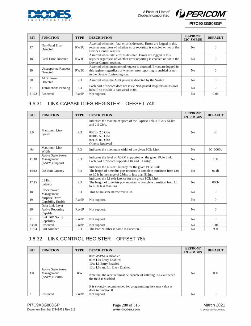
PI7C9X3G808GP Page 280 of 315 March 2021
Document Number DS43471 Rev 1-2 www.diodes.com © Diodes Incorporated
PI7C9X3G808GP
BIT FUNCTION TYPE DESCRIPTION EEPROM/
I2C-SMBUS DEFAULT
17 Non-Fatal Error Detected
RW1C Asserted when non-fatal error is detected. Errors are logged in this register regardless of whether error reporting is enabled or not in the
Device Control register.
No 0
18 Fatal Error Detected RW1C Asserted when fatal error is detected. Errors are logged in this register regardless of whether error reporting is enabled or not in the
Device Control register.
No 0
19 Unsupported Request Detected
RW1C
Asserted when unsupported request is detected. Errors are logged in
this register regardless of whether error reporting is enabled or not
in the Device Control register.
No 0
20 AUX Power
Detected RO Asserted when the AUX power is detected by the Switch No 0
21 Transactions Pending RO Each port of Switch does not issue Non-posted Requests on its own
behalf, so this bit is hardwired to 0b. No 0
31:22 Reserved RsvdP Not support. No 0-0h
9.6.31 LINK CAPABILITIES REGISTER – OFFSET 74h
BIT FUNCTION TYPE DESCRIPTION EEPROM/
I2C-SMBUS DEFAULT
3:0 Maximum Link
Speed RO
Indicates the maximum speed of the Express link is 8Gb/s, 5Gb/s
and 2.5 Gb/s.
0001b: 2.5 Gb/s 0010b: 5.0 Gb/s
0011b: 8.0 Gb/s
Others: Reserved
No 3h
9:4 Maximum Link
Width RO Indicates the maximum width of the given PCIe Link. No 00_0000b
11:10 Active State Power Management
(ASPM) Support
RO Indicates the level of ASPM supported on the given PCIe Link.
Each port of Switch supports L0s and L1 entry. No 10b
14:12 L0s Exit Latency RO Indicates the L0s exit latency for the given PCIe Link. The length of time this port requires to complete transition from L0s
to L0 is in the range of 256ns to less than 512ns.
No 011b
17:15 L1 Exit
Latency RO
Indicates the L1 exit latency for the given PCIe Link. The length of time this port requires to complete transition from L1
to L0 is less than 1us.
No 000b
18 Clock Power Management
RO This bit must be hardwired to 0b. No 0
19 Surprise Down
Capability Enable RsvdP Not support. No 0
20
Data Link Layer
Active Reporting
Capable
RsvdP Not support. No 0
21 Link BW Notify
Capability RsvdP Not support. No 0
23:20 Reserved RsvdP Not support. No 0-0h
31:24 Port Number RO The Port Number is same as Function 0 No 90h
9.6.32 LINK CONTROL REGISTER – OFFSET 78h
BIT FUNCTION TYPE DESCRIPTION EEPROM/
I2C-SMBUS DEFAULT
1:0
Active State Power
Management
(ASPM) Control
RW
00b: ASPM is Disabled
01b: L0s Entry Enabled 10b: L1 Entry Enabled
11b: L0s and L1 Entry Enabled
Note that the receiver must be capable of entering L0s even when
the field is disabled
It is strongly recommended for programming the same value as
does in function 0.
No 00b
2 Reserved RsvdP Not support. No 0

PI7C9X3G808GP Page 281 of 315 March 2021
Document Number DS43471 Rev 1-2 www.diodes.com © Diodes Incorporated
PI7C9X3G808GP
BIT FUNCTION TYPE DESCRIPTION EEPROM/
I2C-SMBUS DEFAULT
3 Read Completion Boundary (RCB)
RO The function does not implement RCB. Returns ‘0’ when read. No 0
4 Link Disable RsvdP Not supported. No 0
5 Retrain Link RsvdP Not supported. No 0
6 Common Clock
Configuration RO
0b: The components at both ends of a link are operating with
synchronous reference clock.
1b: The components at both ends of a link are operating with a distributed common reference clock
It is strongly recommended for programming the same value as
does in function 0.
No 0
7 Extended Synch RO
When set, it transmits 4096 FTS ordered sets in the L0s state for
entering L0 state and transmits 1024 TS1 ordered sets in the L1
state for entering L0 state.
If any function has this bit set, then the component must transmit
additional ordering set when leaving L0s or when in Recovery.
No 0
8 Enable Clock Power Management
RsvdP Not support. No 0
9 HW Autonomous
Width Disable RO Reset to 0b. No 0
10
Link Bandwidth
Management
Interrupt Enable
RO Reset to 0b. No 0
11
Link Autonomous
Bandwidth Interrupt Enable
RO Reset to 0b. No 0
15:12 Reserved RsvdP Not support. No 00h
9.6.33 LINK STATUS REGISTER – OFFSET 78h
BIT FUNCTION TYPE DESCRIPTION EEPROM/
I2C-SMBUS DEFAULT
19:16 Link Speed RO
Indicate the negotiated speed of the Express link.
0001b: 2.5 Gb/s.
0010b: 5.0 Gb/s 0011b: 8.0 Gb/s
Others: Reserved
No 0h
25:20 Negotiated Link Width
RO Indicates the negotiated width of the given PCIe link. No 00_0000b
26 Training Error RsvdP Not supported. No 0
27 Link Training RsvdP Not supported. No 0
28 Slot Clock
Configuration RO
0b: the function uses an independent clock correspective of the presence of a reference on the connector
1b: the function uses the same reference clock that the platform
provides on the connector
For multi-function endpoint, each function must report the same the same value as function 0.
No 0
29 Data Link Layer
Link Active RsvdP Not support. No 0
30 Link Bandwidth
Management Status RO Reset to 0b. No 0
31 Link Autonomous Bandwidth Status
RO Reset to 0b. No 0
9.6.34 DEVICE CAPABILITIES REGISTER 2 – OFFSET 8Ch
BIT FUNCTION TYPE DESCRIPTION EEPROM/
I2C-SMBUS DEFAULT
3:0 CTO Range RO Completion Timeout Ranges: Support Range A (i.e. 50us to 10ms) Yes 0001b

PI7C9X3G808GP Page 282 of 315 March 2021
Document Number DS43471 Rev 1-2 www.diodes.com © Diodes Incorporated
PI7C9X3G808GP
BIT FUNCTION TYPE DESCRIPTION EEPROM/
I2C-SMBUS DEFAULT
4 CTO Disable RO Completion Timeout Disable: Not supported. Returned 0 when read.
Yes 0
5 ARI Forwarding
Supported RO
0b: ARI forwarding is Not supported
1b: ARI forwarding is supported Yes 1
6 Reserved RsvdP Not support. No 0
10:7 Reserved RsvdP Not support. No 0-0h
11 LTR Mechanism Supported
RO A value of 1b indicates support for the optional Latency Tolerance Reporting (LTR) mechanism.
Yes 0
17:12 Reserved RsvdP Not support. No 0-0h
19:18 OBFF Supported RO This field indicates if OBFF is supported. Yes 00b
31:20 Reserved RsvdP Not support. No 000h
9.6.35 DEVICE CONTROL and STATUS REGISTER 2 – OFFSET 90h
BIT FUNCTION TYPE DESCRIPTION EEPROM/
I2C-SMBUS DEFAULT
3:0 CTO Value RW
Completion Timeout Value: For Range A supported, the valid values are as follows.
0000b: 50us to 50ms
0001b: 50us to 100us
0010b: 1ms to 10ms 0101b: 16ms to 55ms
0110b: 65ms to 210ms
The default value is 0000b, which represents a range of 50us to
50ms.
No 0000b
4 CTO Disable RW Completion Timeout Disable: Not supported.
Returned 0 when read. No 0
31:5 Reserved RsvdP Not support. No 00000h
9.6.36 LINK CAPABILITY REGISTER 2 – OFFSET 94h
BIT FUNCTION TYPE DESCRIPTION EEPROM/
I2C-SMBUS DEFAULT
0 Reserved RsvdP Not support. No 0
7:1 Supported Link
Speeds Vector RO
This field indicates the supported Link speed of the associated Port.
bit[0]… 2.5 GT/s
bit[1]… 5.0 GT/s
bit[2]… 8.0 GT/s bit[6:3]… RsvdP
No 0000_111b
8 Crosslink Supported RO 0b: Crosslink is Not supported
1b: Crosslink is supported No 0
31:9 Reserved RsvdP Not support. No 0-0b
9.6.37 LINK CONTROL REGISTER 2 – OFFSET 98h
BIT FUNCTION TYPE DESCRIPTION EEPROM/
I2C-SMBUS DEFAULT
3:0 Target Link Speed RO
0001b: 2.5GT/s link speed is supported
0010b: 5.0GT/s link speed is supported 0011b: 8.0GT/s link speed is supported
Others: reserved.
No 3h
4 Enter Compliance RO 1b: enter compliance No 0
5 HW_AutoSpeed_Dis RO
When set, this bit disables hardware from changing the link speed
for device-specific reasons other than attempting to correct
unreliable link operation by reducing link speed.
No 0
6 Select_Deemp RO
Valid for downstream ports only.
0b: Select -3.5db de-emphasis 1b: Select -6.0 db de-emphasis
No 0

PI7C9X3G808GP Page 283 of 315 March 2021
Document Number DS43471 Rev 1-2 www.diodes.com © Diodes Incorporated
PI7C9X3G808GP
BIT FUNCTION TYPE DESCRIPTION EEPROM/
I2C-SMBUS DEFAULT
9:7 Tran_Margin RO This field controls the value of the non-deemphasized voltage level at the transmitter pins.
No 000b
10 Enter Modify Compliance
RO
Valid for upstream port only.
When set, the device transmits modified compliance pattern if the
LTSSM enters Polling.Compliance substate.
No 0
11 Compliance SOS RO
Valid for upstream port only.
When set, the LTSSM is required to send SKP Ordered Sets between sequences when sending the Compliance Pattern or
Modified Compliance Pattern.
No 0
15:12 Compliance Preset/De-
emphasis RO This field is intended for debug and compliance testing purpose. No 0000b
9.6.38 LINK STATUS REGISTER 2 – OFFSET 98h
BIT FUNCTION TYPE DESCRIPTION EEPROM/
I2C-SMBUS DEFAULT
16 Current De-emphasis level
RO 0b: -6dB 1b: -3.5dB
No 0
31:17 Link status 2 RO Reset to 0. No 0-0h
9.6.39 SSID/SSVID CAPABILITIES REGISTER – OFFSET A4h
BIT FUNCTION TYPE DESCRIPTION EEPROM/
I2C-SMBUS DEFAULT
7:0 SSID/SSVID
Capabilities ID RO Read as 0Dh to indicate that this is SSID/SSVID capability register. No 0Dh
15:8 Next Item Pointer RO Read as 00h. No other ECP registers. No 00h
31:16 Reserved RsvdP Not support. No 0000h
9.6.40 SUBSYSTEM VENDOR ID REGISTER – OFFSET A8h
BIT FUNCTION TYPE DESCRIPTION EEPROM/
I2C-SMBUS DEFAULT
15:0 SSVID RO It indicates the sub-system vendor id. No 12D8h
9.6.41 SUBSYSTEM ID REGISTER – OFFSET A8h
BIT FUNCTION TYPE DESCRIPTION EEPROM/
I2C-SMBUS DEFAULT
31:16 SSID RO It indicates the sub-system device id. No C008h
9.6.42 PCI EXPRESS ADVANCED ERROR REPORTING ENHANCED CAPABILITY HEADER REGISTER – OFFSET 100h
BIT FUNCTION TYPE DESCRIPTION EEPROM/
I2C-SMBUS DEFAULT
15:0 Extended Capabilities ID
RO Read as 0001h to indicate that this is PCI express extended capability register for advance error reporting.
No 0001h
19:16 Capability Version RO Read as 1h. No 1h
31:20 Next Capability Offset
RO No ECP No 000h
9.6.43 UNCORRECTABLE ERROR STATUS REGISTER – OFFSET 104h
BIT FUNCTION TYPE DESCRIPTION EEPROM/
I2C-SMBUS DEFAULT
0 Training Error Status RW1C When set, indicates that the Training Error event has occurred. No 0

PI7C9X3G808GP Page 284 of 315 March 2021
Document Number DS43471 Rev 1-2 www.diodes.com © Diodes Incorporated
PI7C9X3G808GP
BIT FUNCTION TYPE DESCRIPTION EEPROM/
I2C-SMBUS DEFAULT
3:1 Reserved RsvdP Not support. No 000
4 Data Link Protocol
Error Status RW1C
When set, indicates that the Data Link Protocol Error event has
occurred. No 0
5 Surprise Down Error
Status RW1C
When set, indicates that the Surprise Down Error event has occurred.
Valid for Downstream ports only.
No 0
11:6 Reserved RsvdP Not support. No 0-0b
12 Poisoned TLP Status RW1C When set, indicates that a Poisoned TLP has been received or
generated. No 0
13 Flow Control
Protocol Error Status RW1C
When set, indicates that the Flow Control Protocol Error event has
occurred. No 0
14 Completion Timeout Status
RW1C When set, indicates that the Completion Timeout event has occurred.
No 0
15 Completer
AbortStatus RW1C
When set, indicates that the Completer Abort event has occurred.
No 0
16 Unexpected
Completion Status RW1C
When set, indicates that the Unexpected Completion event has
occurred. No 0
17 Receiver Overflow Status
RW1C When set, indicates that the Receiver Overflow event has occurred. No 0
18 Malformed TLP
Status RW1C
When set, indicates that a Malformed TLP has been received.
No 0
19 ECRC Error Status RW1C When set, indicates that an ECRC Error has been detected.
No 0
20 Unsupported Request
Error Status RW1C
When set, indicates that an Unsupported Request event has
occurred. No 0
21 ACS Violation Status RW1C
When set, indicates that an ACS Violation event has occurred
Valid for Downstream ports only.
No 0
22 Internal Error Status RW1C When set, indicates that an Internal Error has occurred. No 0
23 MC Blocked TLP
Status RW1C When set, indicates that an MC Blocked TLP event has occurred. No 0
24 AtomicOp Egress
Blocked Status RW1C
When set, indicates that an AtomicOp Egress Blocked event has
occurred. No 0
31:25 Reserved RsvdP Not support. No 0000_000b
9.6.44 UNCORRECTABLE ERROR MASK REGISTER – OFFSET 108h
BIT FUNCTION TYPE DESCRIPTION EEPROM/
I2C-SMBUS DEFAULT
0 Training Error Mask RW When set, the Training Error event is not logged in the Header Log register and not issued as an Error Message to RC either.
No 0
3:1 Reserved RsvdP Not support. No 000b
4 Data Link Protocol
Error Mask RW
When set, the Data Link Protocol Error event is not logged in the Header Log register and not issued as an Error Message to RC
either.
No 0
5 Surprise Down Error
Mask RW
When set, Surprise Down Error event is not logged in the Header Log register and not issued as an Error Message to RC either.
Valid for Downstream ports only.
No 0
11:6 Reserved RsvdP Not support. No 0-0b
12 Poisoned TLP Mask RW
When set, an event of Poisoned TLP has been received or generated
is not logged in the Header Log register and not issued as an Error Message to RC either.
No 0
13 Flow Control
Protocol Error Mask RW
When set, the Flow Control Protocol Error event is not logged in the
Header Log register and not issued as an Error Message to RC either.
No 0
14 Completion Timeout
Mask RW
When set, the Completion Timeout event is not logged in the
Header Log register and not issued as an Error Message to RC either.
No 0
15 Completer
AbortMask RW
When set, the Completer Abort event is not logged in the Header
Log register and not issued as an Error Message to RC either.
No 0

PI7C9X3G808GP Page 285 of 315 March 2021
Document Number DS43471 Rev 1-2 www.diodes.com © Diodes Incorporated
PI7C9X3G808GP
BIT FUNCTION TYPE DESCRIPTION EEPROM/
I2C-SMBUS DEFAULT
16 Unexpected Completion Mask
RW When set, the Unexpected Completion event is not logged in the Header Log register and not issued as an Error Message to RC
either.
No 0
17 Receiver Overflow Mask
RW When set, the Receiver Overflow event is not logged in the Header Log register and not issued as an Error Message to RC either.
No 0
18 Malformed TLP
Mask RW
When set, an event of Malformed TLP has been received is not logged in the Header Log register and not issued as an Error
Message to RC either.
No 0
19 ECRC Error Mask RW When set, an event of ECRC Error has been detected is not logged in the Header Log register and not issued as an Error Message to
RC either.
No 0
20 Unsupported Request
Error Mask RW
When set, the Unsupported Request event is not logged in the
Header Log register and not issued as an Error Message to RC
either.
No 0
21 ACS Violation Mask RW
When set, the ACS Violation event is not logged in the Header Log register and not issued as an Error Message to RC either.
Valid for Downstream ports only.
No 0
22 Internal Error Mask RW When set, the Internal Error is not logged in the Header Log register
and not issued as an Error Message to RC either. No 1
23 MC Blocked TLP Mask
RW When set, the MC Blocked TLP event is not logged in the Header Log register and not issued as an Error Message to RC either.
No 0
24 AtomicOp Egress
Blocked Mask RW
When set, the AtomicOp Egress Blocked event is not logged in the
Header Log register and not issued as an Error Message to RC either.
No 0
31:25 Reserved RsvdP Not support. No 0000_000b
9.6.45 UNCORRECTABLE ERROR SEVERITY REGISTER – OFFSET 10Ch
BIT FUNCTION TYPE DESCRIPTION EEPROM/
I2C-SMBUS DEFAULT
0 Training Error Severity
RW 0b: Non-Fatal 1b: Fatal
No 1
3:1 Reserved RsvdP Not support. No 000b
4 Data Link Protocol
Error Severity RW
0b: Non-Fatal
1b: Fatal No 1
5 Surprise Down Error
Severity RW
0b: Non-Fatal
1b: Fatal No 1
11:6 Reserved RsvdP Not support. No 0-0b
12 Poisoned TLP Severity
RW 0b: Non-Fatal 1b: Fatal
No 0
13
Flow Control
Protocol Error
Severity
RW 0b: Non-Fatal
1b: Fatal No 1
14 Completion Timeout Error Severity
RW 0b: Non-Fatal 1b: Fatal
No 0
15 Completer
AbortSeverity RW
0b: Non-Fatal
1b: Fatal No 0
16 Unexpected Completion Severity
RW 0b: Non-Fatal 1b: Fatal
No 0
17 Receiver Overflow
Severity RW
0b: Non-Fatal
1b: Fatal No 1
18 Malformed TLP
Severity RW
0b: Non-Fatal
1b: Fatal No 1
19 ECRC Error Severity RW 0b: Non-Fatal 1b: Fatal
No 0
20 Unsupported Request
Error Severity RW
0b: Non-Fatal
1b: Fatal No 0
21 ACS Violation
Severity RW
0b: Non-Fatal
1b: Fatal No 0
22 Internal Error Severity
RW 0b: Non-Fatal 1b: Fatal
No 1
23 MC Blocked TLP
Severity RW
0b: Non-Fatal
1b: Fatal No 0

PI7C9X3G808GP Page 286 of 315 March 2021
Document Number DS43471 Rev 1-2 www.diodes.com © Diodes Incorporated
PI7C9X3G808GP
BIT FUNCTION TYPE DESCRIPTION EEPROM/
I2C-SMBUS DEFAULT
24 AtomicOp Egress Blocked Severity
RW 0b: Non-Fatal 1b: Fatal
No 0
31:25 Reserved RsvdP Not support. No 0000_000b
9.6.46 CORRECTABLE ERROR STATUS REGISTER – OFFSET 110h
BIT FUNCTION TYPE DESCRIPTION EEPROM/
I2C-SMBUS DEFAULT
0 Receiver Error Status RW1C When set, the Receiver Error event is detected. No 0
5:1 Reserved RsvdP Not support. No 0_000b
6 Bad TLPStatus RW1C When set, the event of Bad TLP has been received is detected. No 0
7 Bad DLLP Status RW1C When set, the event of Bad DLLP has been received is detected. No 0
8 REPLAY_NUM Rollover status
RW1C When set, the REPLAY_NUM Rollover event is detected. No 0
11:9 Reserved RsvdP Not support. No 000b
12 Replay Timer
Timeout status RW1C When set, the Replay Timer Timeout event is detected. No 0
13 Advisory Non-Fatal
Error status RW1C When set, the Advisory Non-Fatal Error event is detected. No 0
31:14 Reserved RsvdP Not support. No 0-0h
9.6.47 CORRECTABLE ERROR MASK REGISTER – OFFSET 114h
BIT FUNCTION TYPE DESCRIPTION EEPROM/
I2C-SMBUS DEFAULT
0 Receiver Error Mask RW When set, the Receiver Error event is not logged in the Header Log
register and not issued as an Error Message to RC either. No 0
5:1 Reserved RsvdP Not support. No 0_000b
6 Bad TLPMask RW When set, the event of Bad TLP has been received is not logged in the Header Log register and not issued as an Error Message to RC
either.
No 0
7 Bad DLLP Mask RW When set, the event of Bad DLLP has been received is not logged in the Header Log register and not issued as an Error Message to RC
either.
No 0
8 REPLAY_NUM Rollover Mask
RW When set, the REPLAY_NUM Rollover event is not logged in the Header Log register and not issued as an Error Message to RC
either.
No 0
11:9 Reserved RsvdP Not support. No 000b
12 Replay Timer Timeout Mask
RW
When set, the Replay Timer Timeout event is not logged in the
Header Log register and not issued as an Error Message to RC either.
No 0
13 Advisory Non-Fatal Error Mask
RW
When set, the Advisory Non-Fatal Error event is not logged in the
Header Long register and not issued as an Error Message to RC either.
No 1
31:14 Reserved RsvdP Not support. No 0-0h
9.6.48 ADVANCE ERROR CAPABILITIES AND CONTROL REGISTER – OFFSET 118h
BIT FUNCTION TYPE DESCRIPTION EEPROM/
I2C-SMBUS DEFAULT
4:0 First Error Pointer RO It indicates the bit position of the first error reported in the
Uncorrectable Error Status register. No 0_0000b
5 ECRC Generation
Capable RO
When set, it indicates the Switch has the capability to generate
ECRC. No 1
6 ECRC Generation Enable
RW When set, it enables the generation of ECRC when needed. No 0
7 ECRC Check
Capable RO When set, it indicates the Switch has the capability to check ECRC. No 1
8 ECRC Check Enable RW When set, the function of checking ECRC is enabled. No 0
9 Multiple Header
Recording Capable RO Not support multiple header recording capability. No 0

PI7C9X3G808GP Page 287 of 315 March 2021
Document Number DS43471 Rev 1-2 www.diodes.com © Diodes Incorporated
PI7C9X3G808GP
BIT FUNCTION TYPE DESCRIPTION EEPROM/
I2C-SMBUS DEFAULT
31:10 Reserved RsvdP Not support. No 0-0h
9.6.49 HEADER LOG REGISTER – OFFSET From 11Ch to 128h
BIT FUNCTION TYPE DESCRIPTION EEPROM/
I2C-SMBUS DEFAULT
31:0 1st DWORD RO Hold the 1st DWORD of TLP Header. The Head byte is in big
endian. No 0000_0000h
63:32 2nd DWORD RO Hold the 2nd DWORD of TLP Header. The Head byte is in big endian.
No 0000_0000h
95:64 3rd DWORD RO Hold the 3rd DWORD of TLP Header. The Head byte is in big
endian. No 0000_0000h
127:96 4th DWORD RO Hold the 4th DWORD of TLP Header. The Head byte is in big
endian. No 0000_0000h

PI7C9X3G808GP Page 288 of 315 March 2021
Document Number DS43471 Rev 1-2 www.diodes.com © Diodes Incorporated
PI7C9X3G808GP
9.7 DMA ENGINE INTERFACE REGISTERS
To enable DMA function, the packet switch defines a set of interface registers for software to control the DMA engine
and monitor the status of DMA transfer. There are two DMA engines (DMA_0 and DMA_1) in this Switch to face
either one common or two different CPU domains respectively, so it defines an independent interface for software to
access its own registers in its own CPU domain. The interface registers contain per-channel DMA ontrol and status
registers, descriptor ownership registers, descriptor pointer registersand property registers (such as max payload size,
max read request size and bus number of CDEP port etc.) for cross-domain DMA transfer.
The interface registers are mapped to multiple 256-byte register blocks in memory mode and each 256-byte register
block represents one channel. The register blocks can be accessed by the DMA Memory Base Address, which is
obtained by DMA Base Address Register 0 (Func1, CFG offset 10h or Func2, CFG offset 10h based upon different
DMA mode selection, and please note that each DMA engine is viewed as a PCIe function by enumeration).
Table 9-12: DMA Base Address in Memory Mode when DMA channels pertaining to the same host domain DMA Engine DMA Memory Base Address
Upstream Port CSR for Channel 0 Upstream Port BAR0 + 0000h
Upstream Port CSR for Channel 1 Upstream Port BAR0 + 0100h
N/A Reserved
N/A Reserved
Upstream Port CSR for Channel 4 Upstream Port BAR0 + 0400h
Upstream Port CSR for Channel 5 Upstream Port BAR0 + 0500h
N/A Reserved
N/A Reserved
Table 9-13: DMA Base Address in Memory Mode when DMA channels pertaining to different host domain DMA Engine DMA Memory Base Address
Upstream Port CSR for Channel 0 Upstream Port BAR0 + 0000h
Upstream Port CSR for Channel 4 Upstream Port BAR0 + 0400h
CDEP CSR for Channel 0 CDEP BAR0 + 0000h
CDEP CSR for Channel 4 CDEP BAR0 + 0400h
Following is a summary of addressing map for interface registers. Please note that the max.length for read/write
register only supports 4 bytes.
31 –24 23 – 16 15 – 8 7 –0 BYTE OFFSET
DMA Status 0 DMA Control 0 00h
Descriptor Ownership 0 04h
Descriptor Ownership 1 08h
Channel Descriptor Ring Base Pointer (Low 32-bit) 0Ch
ChannelDescriptor Ring Base Pointer (High 32-bit) 10h
Channel Descriptor Current Pointer (Offset from Base Pointer) 14h
Channel Transfer Count Status ofCurrent Descriptor Pointer 18h
Channel Gap Time Control Reserved 1Ch
DMA Status 1 DMA Control 1 20h
Channel Descriptor Ring Size for Prefetch 24h
Domain 0~3 Max. Payload Size and Read Request Size 28h
Domain 4~7 Max. Payload Size and Read Request Size 2Ch
Domain 8~11 Max. Payload Size and Read Request Size 30h
Domain 0~3 Bus Number (Global) 34h
Domain 4~7 Bus Number (Global) 38h
Domain 8~11 Bus Number (Global) 3Ch
User Defined Attributes for DMA Operation 40h
Channel Uncorrectable Error Status 44h
Reserved 48h ~ 50h
DMA Read Threshold Control 5Ch
Reserved 60h~84h
DMA Hardware Control 0 88h
DMA Hardware Control 1 (Global) 8Ch
Reserved 90h ~ FFh

PI7C9X3G808GP Page 289 of 315 March 2021
Document Number DS43471 Rev 1-2 www.diodes.com © Diodes Incorporated
PI7C9X3G808GP
9.7.1 DMA CONTROL AND STATUS REGISTER 0 – OFFSET 00h
BIT FUNCTION TYPE DESCRIPTION DEFAULT
0 No Snooping Mode RW
Configuration of No Snooping.
0b: Disable no snooping 1b: Enable no snooping
0
1 Address Format RW
Indicate the addressing system a DMA operation is riding on.
0b: 32-bit addressing system
1b: 64-bit addressing system
0
2 CDEP Mapping Enable
RW
Mapping the CDEP channel of another DMA engine to the channel of current DMA
engine. This field has to be programmed for inter-processor domain data transfer
model.
0b: No Mapping (All DMA channels are managed by Root Host)
1b: Mapping to remote channel, The value is only for physical channels (i.e. channel ID are 0 and 4)
When mapping value is not zero, the remote DMA shall be active.
0
4:3 CDEP Mapping
Channel RW
Select mapping remote physical channel ID.
00b: physical channel 0 (DMA 0 CH 0)
01b: physical channel 1 (DMA 0 CH 4)
10b: physical channel 2 (DMA 1 CH 0) 11b physical channel 3 (DMA 1 CH 4)
00b
7:5 CDEP Mapping
Switch RW It need be fixed to 000b. 000b
8 EOT Valid RW
When set, the EOT bit in descriptor is valid under the condition of DMA channels
managed by Root Host only. EOT bit will be updated from 0 to 1 by the switch once the data transfer indicated in that descriptor is ended.
0
16:9 Reserved RsvP Not support. 00h
17 UCE Interrupt
Enable RW When set, Interrupt is issued when detecting Uncorrectable Error 0
18 Error Report Scheme
RW
When clear, DMA reports UCE event without writing DP TLP to destination
address.
When set, DMA reports UCE event after writing DP TLP to destination address
0
27:19 Reserved RsvP Not support. 0-0b
31:28 Channel ID RO Indicate the channel ID is used by which channel of DMA. 0h
9.7.2 DESCRIPTOR OWNERSHIP REGISTER 0 – OFFSET 04h
BIT FUNCTION TYPE DESCRIPTION DEFAULT
31:0 Descriptor
Ownership 0 RW
Indicate the ownership of descriptor 0. That means the owner can access the buffer
pointed by the address field of descriptor 0.
1b: the DMA channel owns the descriptor 0
0b: the DMA driver owns the descriptor 0
After the buffer prepared by DMA driver, it will write “1” to the corresponding
descriptor ownership bit. After the descriptor is done, the DMA channel will clear the corresponding bit to “0”.
0000_000h

PI7C9X3G808GP Page 290 of 315 March 2021
Document Number DS43471 Rev 1-2 www.diodes.com © Diodes Incorporated
PI7C9X3G808GP
9.7.3 DESCRIPTOR OWNERSHIP REGISTER1 – OFFSET 08h
BIT FUNCTION TYPE DESCRIPTION DEFAULT
31:0 Descriptor Ownership 1
RW
Indicate the ownership of descriptor. That means the owner can access the buffer pointed by the address field of descriptor 1.
1b: the DMA channel owns the descriptor 1
0b: the DMA driver owns the descriptor 1
After the buffer prepared by DMA driver, it will write “1” to the corresponding
descriptor ownership bit. After the descriptor is done, the DMA channel will clear the corresponding bit to “0”.
0000_000h
9.7.4 CHANNELDESCRIPTOR RING BASE POINTER (LOW 32-bit)REGISTER – OFFSET 0Ch
BIT FUNCTION TYPE DESCRIPTION DEFAULT
1:0 Reserved RsvdP Not support. 00b
31:2
Descriptor Ring
Base Pointer
(Low 32-bit)
RW
Lower 32-bit of Base Pointer referring to the 1st entry of descriptor ring. It tells
DMA channel where the descriptor is starting at. The base pointer is in 64-bit
alignment.
0000_0000h
9.7.5 CHANNELDESCRIPTOR RING BASE POINTER (HIGH 32-bit) REGISTER – OFFSET 10h
BIT FUNCTION TYPE DESCRIPTION DEFAULT
31:0 Descriptor Ring Base Pointer
(High 32-bit)
RW Upper 32-bit of Base Pointer referring to the 1st entry of descriptor ring if 64-bit
addressing system is used. It tells DMA channel where the descriptor is starting at. 0000_0000h
9.7.6 CHANNEL DESCRIPTOR CURRENT POINTER REGISTER – OFFSET 14h
BIT FUNCTION TYPE DESCRIPTION DEFAULT
11:0
Descriptor Current
Pointer (Offset from Base Pointer)
RO
Indicating the current pointer (Offset from Base Pointer) referring to the descriptor
that is under processing by DMA Engine in terms of index. A maximum of 4096 pointers are allowed.
000h
31:12 Reserved RsvdP Not support. 00000h
9.7.7 CHANNEL TRANSFER COUNT STATUS OF CURRENT DESCRIPTOR POINTER REGISTER – OFFSET 18h
BIT FUNCTION TYPE DESCRIPTION DEFAULT
23:0 Transfer Count
Status RO
Indicating how many byte counts have been not transferred for the current descriptor
pointer. 00_0000h
31:24 Reserved RsvdP Not support. 00h
9.7.8 CHANNEL GAP TIME CONTROL REGISTER – OFFSET 1Ch
BIT FUNCTION TYPE DESCRIPTION DEFAULT
15:0 Write Data Gap
Time Control RW
Control the gap time between DMA writes. It is represented by 16 bits in a unit of
4ns 0000h
31:16 Fetch Data Gap
Time Control RW
Control the gap time between DMA reads. It is represented by 16 bits in a unit of
4ns 0000h

PI7C9X3G808GP Page 291 of 315 March 2021
Document Number DS43471 Rev 1-2 www.diodes.com © Diodes Incorporated
PI7C9X3G808GP
9.7.9 DMA CONTROL AND STATUS REGISTER 1 – OFFSET 20h
BIT FUNCTION TYPE DESCRIPTION DEFAULT
0 DMA Start RW1O
Start DMA operation. 1b: the DMA operation starts to fetch and process the descriptors except the DMA
stop or abort status is on. 0b: the current pointer will be moved to the descriptor ring base pointer or next
descriptor pointer and stop the DMA operation.
This bit can only be written with “1” and will not take effect if written with “0”.
Only when DMA operation is stopped or aborted, this bit will be automatically cleaned to “0”.
0
1 DMA Pause Control RW
Pause DMA Operation.When set, the DMA operation is paused to the next active
descriptor after completing the processing on current descriptor. It means that no more descriptors are processed and prefetched until the “Paused” condition is lifted.
For Host-to-Host DMA operation, the remote-site has to pause its DMA operation at first and ensure the pause done status has been asserted. After that, the local-site is
just allowed to pause DMA operation.
If pause interrupt is enabled and pause control is also enabled, the interruptflagis
asserted until cleared by software.
0
2 DMA Abort Control RW
Abort DMA Operation. When set, the DMA operation drops the current active
descriptor by flushing out all outstanding read commands and discarding all received
completion data. The pointer will move to the next active descriptor. No more descriptors are processed and prefetched until the “Aborted” condition is lifted.
All receiving data will be discarded if DMA abort asserted. Removing abort
condition can only use DMA start control
For Host-to-Host DMA operation, the remote-site has to abort its DMA operation at
first and ensure the abort done status has been asserted. After that, the local-site is just allowed to abort DMA operation.
If abort interrupt is enabled and abort control is also enabled, the interruptflagis asserted until cleared by software.
0
3 DMA Pause
Interrupt Enable RW When set, Interrupt is issued when DMA operation is paused. 0
4 Reserved RsvdP Not support. 0
5 DMA Stop Interrupt
Enable RW When set, Interrupt is issued when DMA operation is stopped. 0
6 DMA Abort Interrupt Enable
RW When set, Interrupt is issued when DMA operation is aborted. 0
7 DMA Stop Control RW1C
Stop DMA Operation. When set, the DMA operation drops the current active descriptor by flushing out all outstanding read commands and discarding all received
completion data. The channel interface registers are all cleaned to default state
except Interrupt flag bit if DMA stop enable is set earlier. No more descriptors are processed and prefetched.
All receiving data will be discarded if DMA stop asserted. Removing stop condition can only use DMA start control
For Host-to-Host DMA operation, the remote-site has to stop its DMA operation at
first and ensure the stop done status has been asserted. After that, the local-site is just
allowed to stop DMA operation.
If stop interrupt is enabled and stop control is also enabled, the interrupt flag is asserted until cleaned by software
0
8 Ownership Flush RW Clear ownership register when DMA operation is stopped. 0
15:9 Reserved RsvdP Not support. 00h
16 DMA Pause Done
Status RO
Indicates the DMA operation is in “Paused” condition.
Removing pause done status can use DMA Pause control. 0
17 DMA Abort Done
Status RO
Indicates the DMA operation is in “Aborted” condition.
Removing abort done status can only use DMA start control. 0
18 DMA Stop Done
Status RO
Indicates the DMA operation is in “Stopped” condition.
Removing Stop done status can only use DMA start control. 1
30:19 Reserved RsvdP Not support. 000h

PI7C9X3G808GP Page 292 of 315 March 2021
Document Number DS43471 Rev 1-2 www.diodes.com © Diodes Incorporated
PI7C9X3G808GP
BIT FUNCTION TYPE DESCRIPTION DEFAULT
31 Interrupt Flag RW1C Indicates the interrupt asserted. 0
9.7.10 CHANNEL DESCRIPTOR RING SIZE FORPREFETCH – OFFSET 24h
BIT FUNCTION TYPE DESCRIPTION DEFAULT
12:0 Descriptor size RW The number of descriptors available for H/W to prefetch is rangedfrom 1 to 4096. 0040h
15:13 Reserved RsvdP Not support. 000b
28:16 Pre-fetch Descriptor Index
RO Index value of next descriptorfor Prefetch 0000h
31:29 Reserved RsvdP Not support. 000b
9.7.11 DOMAIN 0/1/2/3 MAX PAYLOAD SIZE AND READ REQUEST SIZE– OFFSET 28h (Global)
BIT FUNCTION TYPE DESCRIPTION DEFAULT
2:0 Domain 0 Max Payload Size
RW
000b: 128 bytes
001b: 256 bytes 010b: 512 bytes
Other: Reserved
000b
5:3 Domain 0 Read
Request Size RW
000b: 128 bytes 001b: 256 bytes
010b: 512 bytes
011b: 1024 bytes 100b: 2048 bytes
101b: 4096 bytes Other: Reserved
000b
7:6 Reserved RsvdP Not support. 00b
10:8 Domain 1 Max Payload Size
RW
000b: 128 bytes
001b: 256 bytes 010b: 512 bytes
Other: Reserved
000b
13:11 Domain 1 Read
Request Size RW
000b: 128 bytes 001b: 256 bytes
010b: 512 bytes 011b: 1024 bytes
100b: 2048 bytes
101b: 4096 bytes Other: Reserved
000b
15:14 Reserved RsvdP Not support. 00b
18:16 Domain 2 Max
Payload Size RW
000b: 128 bytes 001b: 256 bytes
010b: 512 bytes
Other: Reserved
000b
21:19 Domain 2 Read Request Size
RW
000b: 128 bytes
001b: 256 bytes 010b: 512 bytes
011b: 1024 bytes
100b: 2048 bytes 101b: 4096 bytes
Other: Reserved
000b
23:22 Reserved RsvdP Not support. 00b
26:24 Domain 3 Max
Payload Size RW
000b: 128 bytes
001b: 256 bytes
010b: 512 bytes Other: Reserved
000b
29:27 Domain 3 Read
Request Size RW
000b: 128 bytes
001b: 256 bytes 010b: 512 bytes
011b: 1024 bytes 100b: 2048 bytes
101b: 4096 bytes
Other: Reserved
000b
31:30 Reserved RsvdP Not support. 00b

PI7C9X3G808GP Page 293 of 315 March 2021
Document Number DS43471 Rev 1-2 www.diodes.com © Diodes Incorporated
PI7C9X3G808GP
9.7.12 DOMAIN 4/5/6/7 MAX PAYLOAD SIZE AND READ REQUEST SIZE – OFFSET 2Ch (Global)
BIT FUNCTION TYPE DESCRIPTION DEFAULT
2:0 Domain 4 Max
Payload Size RW
000b: 128 bytes 001b: 256 bytes
010b: 512 bytes Other: Reserved
000b
5:3 Domain 4 Read Request Size
RW
000b: 128 bytes
001b: 256 bytes 010b: 512 bytes
011b: 1024 bytes
100b: 2048 bytes
101b: 4096 bytes
Other: Reserved
000b
7:6 Reserved RsvdP Not support. 00b
10:8 Domain 5 Max
Payload Size RW
000b: 128 bytes
001b: 256 bytes
010b: 512 bytes Other: Reserved
000b
13:11 Domain 5 Read
Request Size RW
000b: 128 bytes
001b: 256 bytes 010b: 512 bytes
011b: 1024 bytes 100b: 2048 bytes
101b: 4096 bytes
Other: Reserved
000b
15:14 Reserved RsvdP Not support. 00b
18:16 Domain 6 Max Payload Size
RW
000b: 128 bytes
001b: 256 bytes 010b: 512 bytes
Other: Reserved
000b
21:19 Domain 6 Read
Request Size RW
000b: 128 bytes 001b: 256 bytes
010b: 512 bytes 011b: 1024 bytes
100b: 2048 bytes
101b: 4096 bytes Other: Reserved
000b
23:22 Reserved RsvdP Not support. 00b
26:24 Domain 7 Max
Payload Size RW
000b: 128 bytes 001b: 256 bytes
010b: 512 bytes
Other: Reserved
000b
29:27 Domain 7 Read
Request Size RW
000b: 128 bytes
001b: 256 bytes
010b: 512 bytes 011b: 1024 bytes
100b: 2048 bytes 101b: 4096 bytes
Other: Reserved
000b
31:30 Reserved RsvdP Not support. 00b
9.7.13 DOMAIN 8/9/10/11 MAX PAYLOAD SIZE AND READ REQUEST SIZE – OFFSET 30h (Global)
BIT FUNCTION TYPE DESCRIPTION DEFAULT
2:0 Domain 8 Max
Payload Size RW
000b: 128 bytes
001b: 256 bytes
010b: 512 bytes
Other: Reserved
000b

PI7C9X3G808GP Page 294 of 315 March 2021
Document Number DS43471 Rev 1-2 www.diodes.com © Diodes Incorporated
PI7C9X3G808GP
BIT FUNCTION TYPE DESCRIPTION DEFAULT
5:3 Domain 8 Read
Request Size RW
000b: 128 bytes
001b: 256 bytes 010b: 512 bytes
011b: 1024 bytes 100b: 2048 bytes
101b: 4096 bytes
Other: Reserved
000b
7:6 Reserved RsvdP Not support. 00b
10:8 Domain 9 Max Payload Size
RW
000b: 128 bytes
001b: 256 bytes 010b: 512 bytes
Other: Reserved
000b
13:11 Domain 9 Read
Request Size RW
000b: 128 bytes
001b: 256 bytes
010b: 512 bytes 011b: 1024 bytes
100b: 2048 bytes
101b: 4096 bytes Other: Reserved
000b
15:14 Reserved RsvdP Not support. 00b
18:16 Domain 10 Max
Payload Size RW
000b: 128 bytes 001b: 256 bytes
010b: 512 bytes
Other: Reserved
000b
21:19 Domain 10 Read Request Size
RW
000b: 128 bytes
001b: 256 bytes
010b: 512 bytes 011b: 1024 bytes
100b: 2048 bytes
101b: 4096 bytes
Other: Reserved
000b
23:22 Reserved RsvdP Not support. 00b
26:24 Domain 11 Max
Payload Size RW
000b: 128 bytes 001b: 256 bytes
010b: 512 bytes Other: Reserved
000b
29:27 Domain 11 Read Request Size
RW
000b: 128 bytes
001b: 256 bytes 010b: 512 bytes
011b: 1024 bytes 100b: 2048 bytes
101b: 4096 bytes
Other: Reserved
000b
31:30 Reserved RsvdP Not support. 00b
9.7.14 DOMAIN 0/1/2/3 BUS NUMBER – OFFSET 34h (Global)
BIT FUNCTION TYPE DESCRIPTION DEFAULT
7:0 Domain 0 Bus Number
RW Indicates Bus Number for Request ID. 00h
15:8 Domain 1 Bus
Number RW Indicates Bus Number for Request ID. 00h
23:16 Domain 2 Bus
Number RW Indicates Bus Number for Request ID. 00h
31:24 Domain 3 Bus Number
RW Indicates Bus Number for Request ID. 00h
9.7.15 DOMAIN 4/5/6/7 BUS NUMBER – OFFSET 38h (Global)
BIT FUNCTION TYPE DESCRIPTION DEFAULT
7:0 Domain 4 Bus Number
RW Indicates Bus Number for Request ID. 00h
8:15 Domain 5 Bus
Number RW Indicates Bus Number for Request ID. 00h
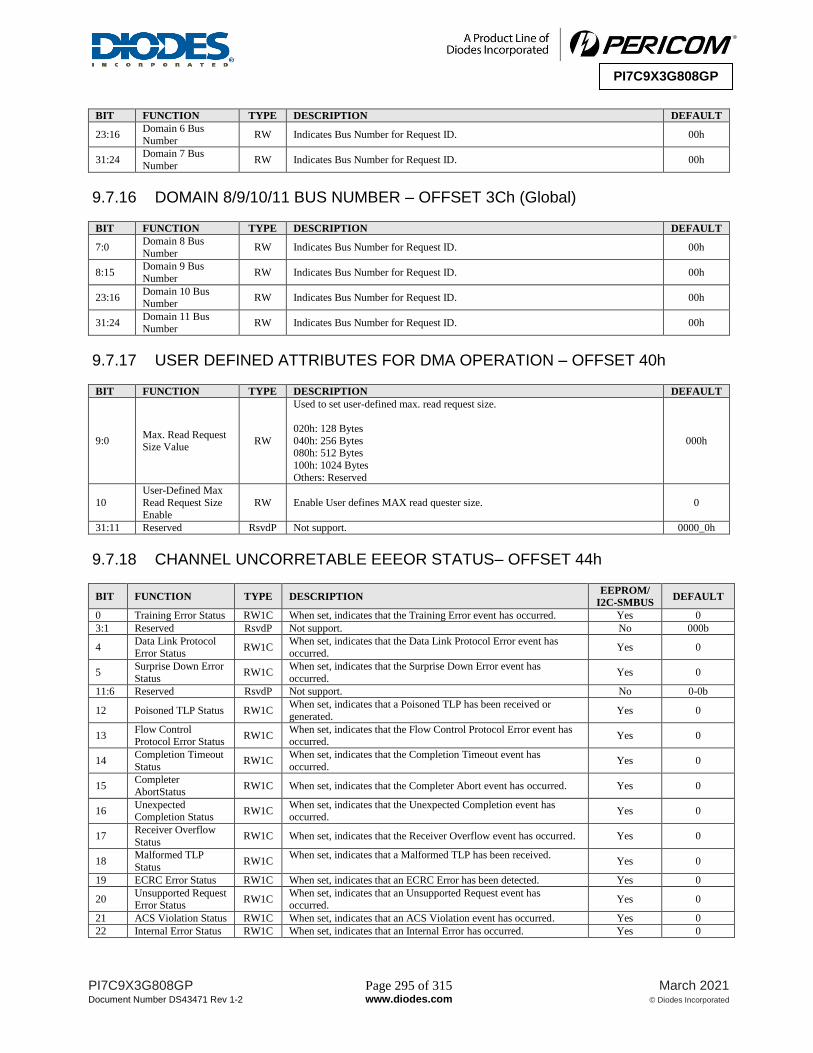
PI7C9X3G808GP Page 295 of 315 March 2021
Document Number DS43471 Rev 1-2 www.diodes.com © Diodes Incorporated
PI7C9X3G808GP
BIT FUNCTION TYPE DESCRIPTION DEFAULT
23:16 Domain 6 Bus
Number RW Indicates Bus Number for Request ID. 00h
31:24 Domain 7 Bus
Number RW Indicates Bus Number for Request ID. 00h
9.7.16 DOMAIN 8/9/10/11 BUS NUMBER – OFFSET 3Ch (Global)
BIT FUNCTION TYPE DESCRIPTION DEFAULT
7:0 Domain 8 Bus
Number RW Indicates Bus Number for Request ID. 00h
8:15 Domain 9 Bus
Number RW Indicates Bus Number for Request ID. 00h
23:16 Domain 10 Bus Number
RW Indicates Bus Number for Request ID. 00h
31:24 Domain 11 Bus
Number RW Indicates Bus Number for Request ID. 00h
9.7.17 USER DEFINED ATTRIBUTES FOR DMA OPERATION – OFFSET 40h
BIT FUNCTION TYPE DESCRIPTION DEFAULT
9:0 Max. Read Request Size Value
RW
Used to set user-defined max. read request size.
020h: 128 Bytes
040h: 256 Bytes 080h: 512 Bytes
100h: 1024 Bytes
Others: Reserved
000h
10
User-Defined Max
Read Request Size
Enable
RW Enable User defines MAX read quester size. 0
31:11 Reserved RsvdP Not support. 0000_0h
9.7.18 CHANNEL UNCORRETABLE EEEOR STATUS– OFFSET 44h
BIT FUNCTION TYPE DESCRIPTION EEPROM/
I2C-SMBUS DEFAULT
0 Training Error Status RW1C When set, indicates that the Training Error event has occurred. Yes 0
3:1 Reserved RsvdP Not support. No 000b
4 Data Link Protocol Error Status
RW1C When set, indicates that the Data Link Protocol Error event has occurred.
Yes 0
5 Surprise Down Error
Status RW1C
When set, indicates that the Surprise Down Error event has
occurred. Yes 0
11:6 Reserved RsvdP Not support. No 0-0b
12 Poisoned TLP Status RW1C When set, indicates that a Poisoned TLP has been received or
generated. Yes 0
13 Flow Control Protocol Error Status
RW1C When set, indicates that the Flow Control Protocol Error event has occurred.
Yes 0
14 Completion Timeout
Status RW1C
When set, indicates that the Completion Timeout event has
occurred. Yes 0
15 Completer
AbortStatus RW1C When set, indicates that the Completer Abort event has occurred. Yes 0
16 Unexpected Completion Status
RW1C When set, indicates that the Unexpected Completion event has occurred.
Yes 0
17 Receiver Overflow
Status RW1C When set, indicates that the Receiver Overflow event has occurred. Yes 0
18 Malformed TLP
Status RW1C
When set, indicates that a Malformed TLP has been received.
Yes 0
19 ECRC Error Status RW1C When set, indicates that an ECRC Error has been detected. Yes 0
20 Unsupported Request Error Status
RW1C When set, indicates that an Unsupported Request event has occurred.
Yes 0
21 ACS Violation Status RW1C When set, indicates that an ACS Violation event has occurred. Yes 0
22 Internal Error Status RW1C When set, indicates that an Internal Error has occurred. Yes 0

PI7C9X3G808GP Page 296 of 315 March 2021
Document Number DS43471 Rev 1-2 www.diodes.com © Diodes Incorporated
PI7C9X3G808GP
BIT FUNCTION TYPE DESCRIPTION EEPROM/
I2C-SMBUS DEFAULT
23 MC Blocked TLP Status
RW1C When set, indicates that an MC Blocked TLP event has occurred. Yes 0
24 AtomicOp Egress
Blocked Status RW1C
When set, indicates that an AtomicOp Egress Blocked event has
occurred. Yes 0
25 Descriptor Error RW1C When set, indicates an Uncorrectable Error happening in descriptor Yes 0
26 Data Buffer Error RW1C When set, indicates an Uncorrectable Error happening in moving
data into DMA buffer. Yes 0
31:27 Reserved RsvdP Not support. No 0000_000b
9.7.19 DMA READ THRESHOLD CONTROL – OFFSET 5Ch
BIT FUNCTION TYPE DESCRIPTION DEFAULT
4:0 Desc_Current_ Arbiter_Sts
RO It will indicate descriptor current arbiter status. 0_0001b
5 Desc_Arbiter_Reset RW When set, it will reset descriptor aribiter. 0
7:6 Reserved RsvdP Not support. 00b
12:8 DMA_Current_ Arbiter_Sts
RO It will indicate DMA current arbiter status. 0_0001b
13 DMA_Arbiter_Reset
RW When set, it will reset DMA aribiter. 0
15:14 Reserved RsvdP Not support. 00b
24:16 Threshold Value RW When threshold control disable is off, the next DMA read won’t be issued until the
threshold value is met. The default value is equivalent to 512 bytes. 80h
25 Threshold Control
Disable RW
When set, DMA read is issued without waiting threshold limit being reached. The
default is to disable threshold control. 1b
31:26 Reserved RsvdP Not support. 0000_0b
9.7.20 DMA HARDWARE CONTROL – OFFSET 88h (Global)
BIT FUNCTION TYPE DESCRIPTION DEFAULT
9:0 DNOC Arbit Delay
Time RW Used to st DNOC Arbit delay time. 0_00h
14:10 Reserved RsvdP Not support 0
15 DNOC Arbit Delay
Time Enable RW
When set, it will enable dnoc arbit delay time function for DMA packets The time
unit is in 2ns. 0
22:16 Back-to-Back
Packet gap time RW
For back-to-back DMA packets, a programmable gap time between continuous
packets can be inserted. The time unit is in 2ns. 00h
23 Back-to-Back Packet gap Time
Enable
RW When set, it will enable back-to-back packet gap time. 0
24 ECRC Check
Enable override RW
When clear, it can override ECRC check enable bit defined in AER control register
from 1 to 0 for DMA packet only 1
25 Arbitration option RW This option bit controls the request/grant protocol between central arbiter and DMA
engine. By default, the DMA request is not asserted until the the last grant released. 1
26 MSI regeneration enable
RW The MSI event will be regenerated once not getting service after a time-out period. When disabled, the MSI will be issued only one time.
1
27 Internal CAM hit
Error Enable RW When set, it will enable CAM hit error function. 1
31:28 Reserved RsvdP Not support 0000b
9.7.21 DMA HARDWARE STATUS – OFFSET 8Ch (Global)
BIT FUNCTION TYPE DESCRIPTION DEFAULT
0 ECRC Check
Enable RO It is a mirror-bit of ECRC Check Enable status in AER control register 0
1 ECRC Generation
Enable RO It is a mirror-bit of ECRC Generation Enable status in AER control register 0
31:2 Reserved RsvdP Not support 0-0b

PI7C9X3G808GP Page 297 of 315 March 2021
Document Number DS43471 Rev 1-2 www.diodes.com © Diodes Incorporated
PI7C9X3G808GP
10 POWER SEQUENCE
As long as PERST# is asserted, all PCI Express functions are held in reset. The main supplies ramp up to their
specified levels (0.95V/1.8V). Sometime during this stabilization time, the REFCLK starts and stabilizes. After
elapsing some time (i.e. 100 us) for the power and clock to become stable, PERST# is deasserted high and the PCI
Express functions can start up.
Figure 10-1 Initial Power-Up Sequence

PI7C9X3G808GP Page 298 of 315 March 2021
Document Number DS43471 Rev 1-2 www.diodes.com © Diodes Incorporated
PI7C9X3G808GP
11 IEEE 1149.1 COMPATIBLE JTAG CONTROLLER
An IEEE 1149.1 compatible Test Access Port (TAP) controller and associated TAP pins are provided to support
boundary scan in PI7C9X3G808GP for board-level continuity test and diagnostics. The TAP pins assigned are TCK,
TDI, TDO, TMS and TRST_L. All digital input, output, input/output pins except TAP pins and SERDES pins are
tested.
11.1 INSTRUCTION REGISTER
The IEEE 1149.1 Test Logic consists of a TAP controller, an instruction register, and a group of test data registers
including Bypass and Boundary Scan registers. The TAP controller is a synchronous 16-state machine driven by the
Test Clock (TCK) and the Test Mode Select (TMS) pins. An independent power on reset circuit is provided to ensure
the machine is in TEST_LOGIC_RESET state at power-up.
PI7C9X3G808GP implements a 5-bit Instruction register to control the operation of the JTAG logic. The defined
instruction codes are shown in the following table. Those bit combinations that are not listed are equivalent to the
BYPASS (1111) instruction.
Table 11-1 Instruction Register Codes
Instruction Operation Code (binary) Register Selected Operation
EXTEST 0000 Boundary Scan Drives / receives off-chip test data
SAMPLE 0010 Boundary Scan Samples inputs
EXTEST_PULSE 0100 Boundary Scan Drives/receives off-chip test data for TX/RX pins
EXTEST_TRAIN 0101 Boundary Scan Drives/receives off-chip test data for TX/RX pins
SCAN_TEST 1010 Internal Private instruction
IDCODE 0001 Device ID Accesses the Device ID register, to read manufacturer ID, part number, and version number
RX_LEVEL 1011 Internal Private instruction
NOC_BIST 0111 Internal Private instruction
MBIST 1101 Internal Private instruction
BYPASS 1111 Bypass Selected Bypass Register
11.2 BYPASS REGISTER
The required bypass register (one-bit shift register) provides the shortest path between TDI and TDO when a bypass
instruction is in effect. This allows rapid movement of test data to and from other components on the board. This path
can be selected when no test operation is being performed on the PI7C9X3G808GP.
11.3 DEVICE ID REGISTER
This register identifies Diodes as the manufacturer of the device and details the part number and revision number for
the device.
Table 11-2 JTAG Device ID Register
Bit Type Value Description
31-28 RO 0001 Version number
27-12 RO 0001011000010110 Last 4 digits (hex) of the die part number
11-1 RO 01000111111 Diodes identifier assigned by JEDEC
0 RO 1 Fixed bit equal to 1

PI7C9X3G808GP Page 299 of 315 March 2021
Document Number DS43471 Rev 1-2 www.diodes.com © Diodes Incorporated
PI7C9X3G808GP
11.4 BOUNDARY SCAN REGISTER
The boundary scan register has a set of serial shift-register cells. A chain of boundary scan cells is formed by connected
the internal signal of the PI7C9X3G808GP package pins. The VDD, VSS, and JTAG pins are not in the boundary scan
chain. The input to the shift register is TDI and the output from the shift register is TDO. There are 4 different types of
boundary scan cells, based on the function of each signal pin.
The boundary scan register cells are dedicated logic and do not have any system function. Data may be loaded into the
boundary scan register master cells from the device input pins and output pin-drivers in parallel by the mandatory
SAMPLE and EXTEST instructions. Parallel loading takes place on the rising edge of TCK.
11.5 JTAG BOUNDARY SCAN REGISTER ORDER
Table 11-3 JTAG Boundary Scan Register Definition Boundary Scan
Register Number Pin Name Ball Location Type Tri-state Control Cell
0 internal
1 internal
2 SDA_I2C L13 bidir 3
3 control
4 SCL_I2C L14 bidir 5
5 control
6 internal
7 internal
8 PERST_L D13 input
9 internal
10 internal
11 PDC_L[7] N4 bidir 12
12 control
13 PDC_L[6] M11 bidir 14
14 control
15 internal
16 internal
17 PDC_L[5] N12 bidir 18
18 control
19 internal
20 internal
21 PDC_L[4] N13 bidir 22
22 control
23 PDC_L[3] N14 bidir 24
24 control
25 PDC_L[2] P12 bidir 26
26 control
27 PDC_L[1] P14 bidir 28
28 control
29 PDC_L[0] P13 bidir 30
30 control
31 PERN[3] A6 observe_only
32 PERP[3] B6 observe_only
33 PETP[3] E6 output2
34 PERN[2] A7 observe_only
35 PERP[2] B7 observe_only
36 PETP[2] E7 output2
37 PERN[1] A9 observe_only
38 PERP[1] B9 observe_only
39 PETP[1] E9 output2
40 PERN[0] A10 observe_only
41 PERP[0] B10 observe_only
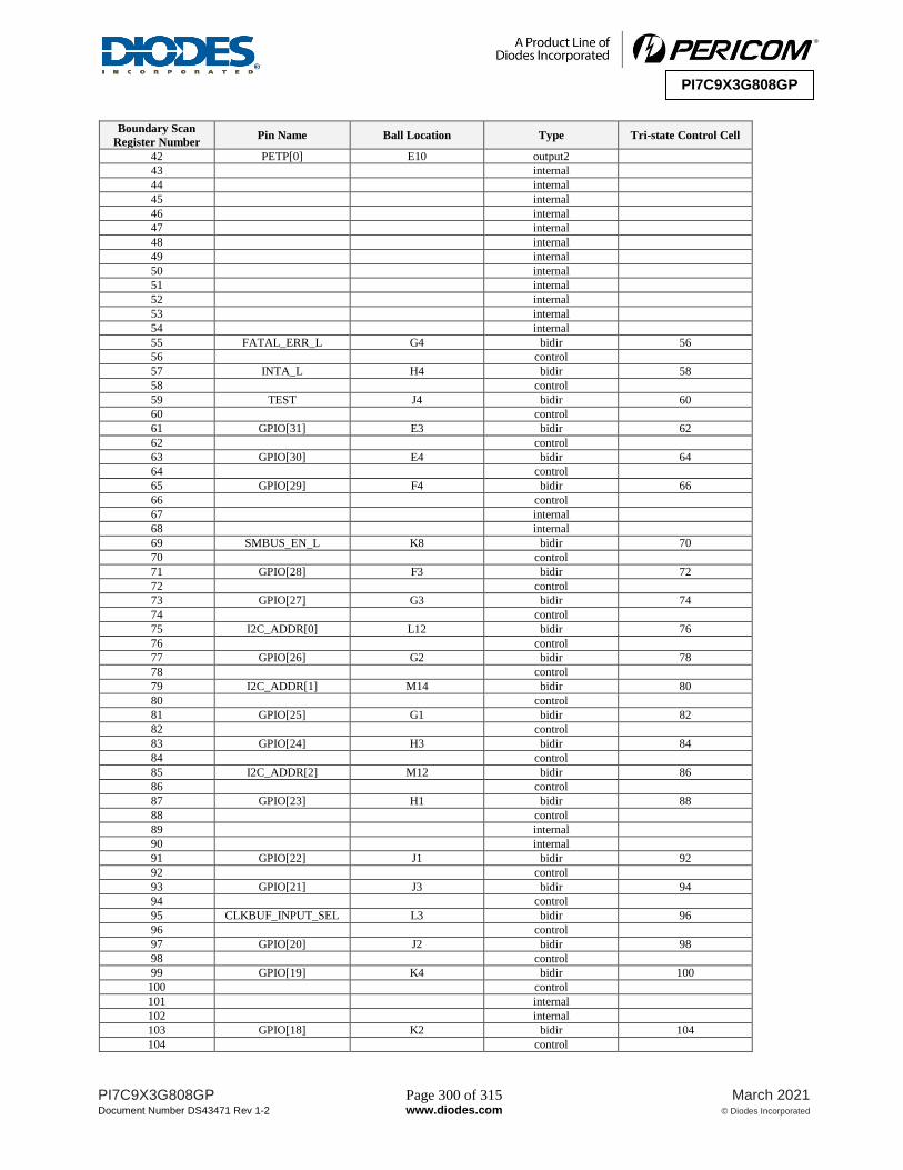
PI7C9X3G808GP Page 300 of 315 March 2021
Document Number DS43471 Rev 1-2 www.diodes.com © Diodes Incorporated
PI7C9X3G808GP
Boundary Scan
Register Number Pin Name Ball Location Type Tri-state Control Cell
42 PETP[0] E10 output2
43 internal
44 internal
45 internal
46 internal
47 internal
48 internal
49 internal
50 internal
51 internal
52 internal
53 internal
54 internal
55 FATAL_ERR_L G4 bidir 56
56 control
57 INTA_L H4 bidir 58
58 control
59 TEST J4 bidir 60
60 control
61 GPIO[31] E3 bidir 62
62 control
63 GPIO[30] E4 bidir 64
64 control
65 GPIO[29] F4 bidir 66
66 control
67 internal
68 internal
69 SMBUS_EN_L K8 bidir 70
70 control
71 GPIO[28] F3 bidir 72
72 control
73 GPIO[27] G3 bidir 74
74 control
75 I2C_ADDR[0] L12 bidir 76
76 control
77 GPIO[26] G2 bidir 78
78 control
79 I2C_ADDR[1] M14 bidir 80
80 control
81 GPIO[25] G1 bidir 82
82 control
83 GPIO[24] H3 bidir 84
84 control
85 I2C_ADDR[2] M12 bidir 86
86 control
87 GPIO[23] H1 bidir 88
88 control
89 internal
90 internal
91 GPIO[22] J1 bidir 92
92 control
93 GPIO[21] J3 bidir 94
94 control
95 CLKBUF_INPUT_SEL L3 bidir 96
96 control
97 GPIO[20] J2 bidir 98
98 control
99 GPIO[19] K4 bidir 100
100 control
101 internal
102 internal
103 GPIO[18] K2 bidir 104
104 control

PI7C9X3G808GP Page 301 of 315 March 2021
Document Number DS43471 Rev 1-2 www.diodes.com © Diodes Incorporated
PI7C9X3G808GP
Boundary Scan
Register Number Pin Name Ball Location Type Tri-state Control Cell
105 GPIO[17] K3 bidir 106
106 control
107 GPIO[16] K1 bidir 108
108 control
109 GPIO[15] L1 bidir 110
110 control
111 GPIO[14] M1 bidir 112
112 control
113 GPIO[13] M3 bidir 114
114 control
115 GPIO[12] M2 bidir 116
116 control
117 GPIO[11] M4 bidir 118
118 control
119 GPIO[10] M5 bidir 120
120 control
121 GPIO[9] N1 bidir 122
122 control
123 GPIO[8] N3 bidir 124
124 control
125 GPIO[7] N2 bidir 126
126 control
127 GPIO[6] D14 bidir 128
128 control
129 GPIO[5] C12 bidir 130
130 control
131 GPIO[3] B13 bidir 132
132 control
133 GPIO[4] C14 bidir 134
134 control
135 GPIO[2] B14 bidir 136
136 control
137 GPIO[1] A12 bidir 138
138 control
139 GPIO[0] A13 bidir 140
140 control
141 PERN[7] P10 observe_only
142 PERP[7] N10 observe_only
143 PETP[7] K10 output2
144 PERN[6] P9 observe_only
145 PERP[6] N9 observe_only
146 PETP[6] K9 output2
147 PERN[5] P7 observe_only
148 PERP[5] N7 observe_only
149 PETP[5] K7 output2
150 PERN[4] P6 observe_only
151 PERP[4] N6 observe_only
152 PETP[4] K6 output2
153 internal
154 internal
155 internal
156 internal
157 internal
158 internal
159 internal
160 internal
161 internal
162 internal
163 internal
164 internal
165 PORTCFG[2] D12 input
166 SHCL_I2C P4 bidir 167
167 control

PI7C9X3G808GP Page 302 of 315 March 2021
Document Number DS43471 Rev 1-2 www.diodes.com © Diodes Incorporated
PI7C9X3G808GP
Boundary Scan
Register Number Pin Name Ball Location Type Tri-state Control Cell
168 PORTCFG[1] C11 input
169 SHPCINT_L P1 bidir 170
170 control
171 PORTCFG[0] B12 input
172 SHDA_I2C P3 bidir 173
173 control
174 internal
175 internal
176 EECS_L K14 bidir 177
177 control
178 EECK K13 bidir 179
179 control
180 EEDO J14 bidir 181
181 control
182 CKMODE E12 bidir 183
183 control
184 EEDI K12 bidir 185
185 control
186 PORTGOOD_L[7] H14 bidir 187
187 control
188 PORTGOOD_L[6] G13 bidir 189
189 control
190 PORTGOOD_L[5] G12 bidir 191
191 control
192 PORTGOOD_L[4] G14 bidir 193
193 control
194 PORTGOOD_L[3] F12 bidir 195
195 control
196 PORTGOOD_L[2] F14 bidir 197
197 control
198 PORTGOOD_L[1] E14 bidir 199
199 control
200 PORTGOOD_L[0] E13 bidir 201
201 control
202 internal
203 internal

PI7C9X3G808GP Page 303 of 315 March 2021
Document Number DS43471 Rev 1-2 www.diodes.com © Diodes Incorporated
PI7C9X3G808GP
12 ELECTRICAL AND TIMING SPECIFICATIONS
12.1 ABSOLUTE MAXIMUM RATINGS
Table 12-1 Absolute Maximum Ratings (Above which the useful life may be impaired. For user guidelines, not tested.)
Item Absolute Max. Rating Storage Temperature -65’C to 150’C
Junction Temperature, Tj 125 oC
Digital core and analog supply voltage to ground potential (VDDC and AVDD) VDDC +10%
Digital I/O and analog high supply voltage to ground potential (VDDR and AVDDH) VDDR + 10%
DC input voltage for Digital I/O signals 2.75V
ESD Rating
Human Body Model (JEDEC Class 2)
Charge Device Model (JEDEC Class 3)
HBM 2KV
CDM 500V
Note:
Stresses greater than those listed under MAXIMUM RATINGS may cause permanent damage to the device. This is a stress rating only
and functional operation of the device at these or any conditions above those indicated in the operational sections of this specification is not implied. Exposure to absolute maximum rating conditions for extended periods of time may affect reliability.
12.2 DC ELECTRICAL CHARACTERISTICS
Table 12-2 DC Electrical Characteristics Symbol Description Min. Typ. Max. Unit VDDC2 Digital Core Power 0.90 0.95 0.99
V
C_VDDR2 Referenc Clock Power 0.90 0.95 0.99
VDDR3 Digital I/O Power 1.71 1.8 1.89
C_VDDR3 Reference Clock Power 1.71 1.8 1.89
VP2 PCI Express Analog Power 0.90 0.95 0.99
VPH3 PCI Express Analog High Voltage Power 1.71 1.8 1.89
VIH Input High Voltage 1.17 1.98
VIL Input Low Voltage -0.3 0.63
VOH Output High Voltage 1.35
VOL Output Low Voltage 0.45
RPU Pull-up Resistor 54K 80K 120K Ω
RPD Pull-down Resistor 55K 95K 176K
RST#Slew1 PERST_L Slew Rate 50 mV/ns
Note:
1. The min. value for PERST_L Slew Rate is 50 mV/ns, which translates to the requirement that the time for PERST_L from 0V
to 2.5V should be less than 50 ns. 2. Peak to peak AC noise < 5% of DC level.
3. Peak to peak AC noise < 3% of DC level.
12.3 PCIE REFERENCE CLOCK REQUIREMENTS
Table 12-1 specifies the voltage/timing requirements and operating characteristics for PCIe PHY (REFCLKP/N[1:0]
and REFCLKP/N[1:0]).
Table 12-3 PCIe Reference Clock Requirement
Application Reference Clock Jitter and Swing Requirements PCIe 1.1 – 2.5 GT/s Refer to the PCI Express 3.0 Card Electromechamical specification.
PCIe 2.1 – 5.0 GT/s Refer to the PCI Express 3.1 base specification.
PCIe 3.1 – 8.0 GT/s Refer to the PCI Express 3.1 base specification.

PI7C9X3G808GP Page 304 of 315 March 2021
Document Number DS43471 Rev 1-2 www.diodes.com © Diodes Incorporated
PI7C9X3G808GP
12.4 INTEGRATED CLOCK BUFFER SPECIFICATIONS
The built-in Ingegrated Reference Clock Buffer of the PI7C9X3G808GP supports eight reference clock outputs Table
12-4 and Table 12-5 specify the voltage/timing requirements and operating characteristics for internal clock buffer
input (REFCLKIP/N and REFCLKIP/N) and outputs (REFCLKOP/N[7:0] and REFCLKOP/N[7:0]).
Table 12-4 Integrated Clock Buffer Input Electrical Characteristics
Symbol Description Min Typ Max Unit VIHDIF Input High Voltage-DIF_IN (Single-ended) 600 800 1150 mV
VILDIF Input Low Voltage-DIF_IN (Single-ended) Vss - 300 0 300 mV
VCOM Input Common Mode Voltage-DIF_IN 300 725 mV
VSWING Input Amplitude Peak-to-Peak (VIHDIF - VILDIF) 300 1450 mV
IIN Input Leakage Current -5 0.01 5 uA
DTIN Input Duty Cycle 45 55 %
JDIFIN Input Jitter – Cycle to Cycle 0 150 ps
FIN Input Frequency 100 MHz
VIL(ASIC) Low-level input voltage 0 V
VIH(ASIC) High-level input voltage 1 V
TR, TF Rise/Fall time of input clock 0.1 RCUI1
Note1: RCUI refers to the reference clock period.
Table 12-5 Integrated Clock Buffer Output Electrical Characteristics
Symbol Description Min Typ Max Unit TR Output Rise Time (20% to 80%) 100 200 500 ps
TF Output Fall Time (80% to 20%) 100 200 500 ps
VHIGH Voltage High Statistical measurement on single-ended
signal using oscilloscope math function
(Scope averaging on)
660 774 850 mV
VLOW Voltage Low -150 18 150 mV
VMAX Max Voltage Measurement on single ended signal using
absolute value (Scope averaging off)
821 1150 mV
VMIN Min Voltage -300 -15 mV
VSWING Voltage Swing (Scope averaging off) 300 1536 mV
VCROSS_ABS Absolute crossing voltage (Scope averaging off) 250 414 550 mV
△VCROSS Variance crossing voltage (Scope averaging off) 13 140 mV
TDCD Duty Cycle Distortion (measured differentially) -3 0 3 %
TPD Skew, Input to Output 1000 3600 4500 ps
TJCC Additive Jitter, Cycle to Cycle 0.1 25 ps (p-p)
TJPHG1 Additive Phase Jitter for PCIe GEN1 0.6 5 ps (rms)
TJPHG2 Additive Phase Jitter for PCIe GEN2 Low Band 10 kHz < f <
1.5 MHz 0.1 0.3 ps (rms)
TJPHG2 Additive Phase Jitter for PCIe GEN2 High Band 1.5 MHz <f <
Nyquist (50 MHz) 0.05 0.1 ps (rms)
TJPHG3 Additive Phase Jitter for PCIe GEN3
(PLL BW of 2 ~ 4 MHz, CDR = 10 MHz) 0.05 0.1 ps (rms)
12.5 COMMON TRANSMITTER PARAMETERS
The following table defines the parameters for transmitters that are common among all three data rates. Parameters are
defined separated for 2.5 GT/s, 5.0 GT/s and 8.0 GT/s implementations.
Table 12-6 Transmitter Specidications
Symbol Parameter 2.5 GT/s 5.0 GT/s 8.0 GT/s Units Comments
UI Unit Interval
399.88 (min)
400.12 (max)
199.94 (min)
200.06 (max)
124.9625 (min)
125.0375 (max) ps
The specified UI is equivalent to a
tolerance of ±300 ppm for each
Refclk source. Period does not
account for SSC induced variations.
See Note 1.

PI7C9X3G808GP Page 305 of 315 March 2021
Document Number DS43471 Rev 1-2 www.diodes.com © Diodes Incorporated
PI7C9X3G808GP
Symbol Parameter 2.5 GT/s 5.0 GT/s 8.0 GT/s Units Comments
BWTX-PLL Tx PLL BW for 2.5 GT/s
22 (max) 1.5 (min)
Not specified Not specified MHz See Note 6.
BWTX-PKG-PLL1
Tx PLL bandwidth
corresponding to
PKGTX-PLL1
Not specified 16 (max)
8 (min)
4 (max)
2 (min) MHz
Second order PLL jitter transfer
bounding function. See Note 6.
BWTX-PKG-PLL2
Tx PLL
bandwidth
corresponding to PKGTX-PLL2
Not specified 16 (max)
5 (min)
5 (max)
2 (min) MHz
Second order PLL jitter transfer
bounding function. See Note 6.
PKGTX-PLL1 Tx PLL peaking Not specified 3.0 (max) 2.0 (Max) dB
PLL BW = 8 MHz (min) @ 5.0
GT/s or BW = 4 MHz (max) @ 8.0 GT/s. See Note 6 and 8.
PKGTX-PLL2 Tx PLL peaking Not specified 1.0 (max) 1.0 (Max) dB
PLL BW = 5 MHz (min) @ 5.0
GT/s or BW = 5 MHz (max) @ 8.0 GT/s. See Note 8.
VTX-DIFF-PP Differenital p-p
Tx voltage swing
0.8 (min)
1.2 (max)
0.8 (min)
1.2 (max) See Table 12-7 VPP
As measured with compliance test
load. Defined as 2*|VTXD+-VTXD-|.
VTX-DIFF-PP-LOW
Low power
differential p-p Tx
voltage swing
0.4 (min) 1.2 (max)
0.4 (min) 1.2 (max)
See Table 12-7 VPP
As measured with compliance test
load. Defined as 2*|VTXD+-VTXD-|.
See Note 9.
VTX-DE-RATIO-3.5dB Tx de-emphasis level ratio
3.0 (min) 4.0 (max)
3.0 (min) 4.0 (max)
See Table 12-7 dB
See PCI Express Base Specification
Revision 3.1, Section 4.3.3.3 and
Note 11.
VTX-DE-RATIO-6dB Tx de-emphasis lebel
N/A 5.5 (min) 6.5 (max)
See Table 12-7 dB
See PCI Express Base Specification
Revision 3.1, Section 4.3.3.3 and Note 11.
TMIN-PULSE Instantaneous lone
pulse width Not specified 0.9 (min) See Table 12-7 UI
Measured relative to rising/falling
pulse. See Note 2, 10 and PCI
Express Base Specification Revision
3.1, Figure 4-38.
TTX-EYE
Transmitter Eye
including all jitter sources
0.75 (min) 0.75 (min) See Table 12-7 UI
Does not include SSC or Refclk jitter. Includes Rj at 10-12. Note that
2.5 GT/s and 5.0 GT/s use different
jitter determination methods.
TTX-EYE-MEDIAN-to-
MAX-JITTER
Maximum time
between the jitter
median and max deviation from the
median
0.125 (max) Not specified Not specified UI
Measured differentially at zero crossing points after applying the
2.5 GT/s clock recovery function. See Note 2.
TTX-HF-DJ-DD Tx deterministic jitter > 1.5 MHz
Not specified 0.15 (max) See Table 12-7 UI Deterministic jitter only. See Notes 2 and 10.
TTX-LF-RMS Tx RMS jitter <
1.5 MHz Not specified 3.0 See Table 12-7
Ps
RMS
Total energy measured over a 10
kHz - 1.5 MHz range.
TRF-MISMATCH Tx rise/fall
mismatch Not specified 0.1 (max) Not specified UI
Measured from 20% to 80%
differentially. See Note 2.
RLTX-DIFF Tx package plus Si differential
return loss
10 (min)
10 (min) for
0.05 -1.25 GHz 8 (min) for >
1.25 - 2.5 GHz
10 (min) for 0.05 -1.25 GHz
8 (min) for > 1.25 - 2.5 GHz
4 (min) for >
2.5 - 4 GHz
dB For details refer to PCI Express Base Specification Revision 3.1,
Figure 4-56.
RLTX-CM Tx package plus Si common mode
return loss
6 (min) for 0.05
- 2.5 GHz
6 (min) for 0.05
- 2.5 GHz
6 (min) for 0.05
- 2.5GHz
3 (min) for 2.5 GHz
dB For details refer to PCI Express Base Specification Revision 3.1,
Figure 4-57.
ZTX-DIFF-DC DC differential Tx
impedance
80 (min)
120 (max) 120 (max) 120 (max) Ω
Low impedance defined during
signaling. Parameter is captured for 5.0 GHz by RLTX-DIFF. The (min)
value is bounded by RLTX-DIFF for
5.0 GT/s and 8.0 GT/s.
VTX-CM-AC-PP
Tx AC peak-peak
common mode
voltage (5.0 GT/s)
Not specified 150 (max) 150 (max) mVPP
At 8.0 GT/s, no more than 50mVPP
in 0.03-500 MHz range. At 5.0GT/s no more than 100mVPP in 0.03-500
MHz range. See Notes 5 and 12.
VTX-CM-AC-P Tx AC peak common mode
20 Not specified Not specified mV See Note 5.

PI7C9X3G808GP Page 306 of 315 March 2021
Document Number DS43471 Rev 1-2 www.diodes.com © Diodes Incorporated
PI7C9X3G808GP
Symbol Parameter 2.5 GT/s 5.0 GT/s 8.0 GT/s Units Comments voltage (2.5 GT/s)
ITX-SHORT
Transmitter short-
circuit current limit
90 (max) 90 (max) 90 (max) mA
The total single-ended current a
transmitter can supply when shorted to ground. See Note 13.
VTX-DC-CM
Transmitter DC
common-mode voltage
0 (min) 3.6 (max)
0 (min) 3.6 (max)
0 (min) 3.6 (max)
V
The allowed DC common-mode
voltage at a transmitter pin under any conditions. See Note 13.
VTX-CM-DC-ACTiVE-
IDLE-DELTA
Absolute Delta of DC Common
Mode Voltage during L0 and
Electrical Idle
0 (min) 100 (max)
0 (min) 100 (max)
0 (min) 100 (max)
mV
|VTX-CM-DC [during L0] – VTX-CM-Idle-DC
[during Electrical Idle]| ≤ 100mV
VTX-CM-DC = DC(avg) of |VTX-D+ + VTX-
D-|/2
VTX-CM-Idle-DC = DC(avg) of |VTX-D+ +
VTX-D-|/2 [Electrical Idle]
VTX-CM-DC-LINE-
DELTA
Absolute Delta of DC Common
Mode Voltage
between D+ and D-
0 (min) 25 (max)
0 (min) 25 (max)
0 (min) 25 (max)
mV
|VTX-CM-DC-D+ [during L0] – VTX-CM-DC-D-
[during L0]| ≤ 25mV
VTX-CM-DC-D+ = DC(avg) of |VTX-D+| [during L0]
VTX-CM-DC-D- = DC(avg) of |VTX-D-|
[during L0].
VTX-IDLE-DIFF-AC-p
Electrical Idle
Differential Peak Output Voltage
0 (min)
20 (max)
0 (min)
20 (max)
0 (min)
20 (max) mV
VTX-IDLE-DIFF-AC-p = |VTX-Idle-D+ - VTX-
Idle-D-| ≤ 20mV. Voltage must be
band pass filtered to remove any DC
component and HF noise. The bandpass is constructed from two
first-order filters, the high pass and low pass 3dB bandwidths are 10
kHz and 1.25 GHz respectively.
VTX-IDLE-DIFF-DC DC Electrical Idle Differential
Output Voltage
Not specified 0 (min)
5 (max)
0 (min)
5 (max) mV
VTX-IDLE-DIFF-DC = |VTX-Idle-D+ - VTX-Idel-
D-| ≤ 5mV. Voltage must be low pass
filtered to remove any AC
component. The low pass filter is first-order with a 3dB bandwidth of
10 kHz.
VTX-RCV-DETECT
The amount of voltage change
allowed during
Receiver Detection
600 (max) 600 (max) 600 (max) mV
The total amount of voltage change in a positive dirction that a
Transmitter can apply to sense whether a low impedance Receiver
is present. Note: Receivers display
substantially different impedance for VIN < 0 vs VIN > 0. See PCI
Express Base Specification Revision 3.1, Table 4-24 for detail
TTX-IDLE-MIN
Minimum time
spent in Electrical Idle
20 (min) 20 (min) 20 (min) ns Minimum time a Transmitter must
be in Electrical Idle.
TTX-IDLE-SET-TO-IDLE
Maximum time to transition to a
valid Electrical Idle after sending
an EIOS
8 (max) 8 (max) 8 (max) ns
After sending the required number
of EIOSs, the Transmitter must meet all Electrical Idel specifications
within this time. This is measured from the end of the last UI of the
last EIOS to the Transmitter in
Electrical Idle.
TTX-IDLE-TO-DIFF-
DATA
Maximum time to
transistion to valid
diff signaling after leaving Electrical
Idle
8 (max) 8 (max) 8 (max) ns
Maximum time to transition to valid diff signaling after leaving Electrical
Idle. This is considered a debounce
time to the Tx.
TCROSSLINK Crosslink random
timeout 1.0 (max) 1.0 (max) 1.0 (max) ms
This random timeout helps resolve potential conflicts in the crosslink
configuration.
LTX-SKEW Lane-to-Lane
Output Skew
500 ps + 2 UI
(max)
500 ps + 4 UI
(max) 500 ps + 6 UI ps
Between any two Lanes within a
single Transmitter.
CTX AC Coupling Capacitor
75 (min) 265 (max)
75 (min) 265 (max)
176 (min) 265 (max)
nF
All Transmitters shall be AC
coupled. The AC coupling is required wither within the media or
within the transmitting component itself. See Note 14.

PI7C9X3G808GP Page 307 of 315 March 2021
Document Number DS43471 Rev 1-2 www.diodes.com © Diodes Incorporated
PI7C9X3G808GP
Note:
1. SSC permits a +0, -5000ppm modulation of the clock frequency ar a modulation rate not to exceed 33 kHz.
2. Measurements at 5.0 GT/s require an oscilloscope with a bandwidth of ≥12.5 GHz, or equivalent, while measurements made at 2.5 GT/s require
a scope with a least 6.2 GHz bandwidth. Measurement at 5.0 GT/s must deconvolve effects of compliance test board to yield an effective measurement at Tx pins. 2.5 GT/s may be measured within 200 mils of Tx device’s pins, although deconvolution is recommended. For
measurement setup details, refer PCI Express Base Specification Revision 3.1, Figure 4-32 to and Figure 4-33. At lease 106 UI of data must be
acquired.
3. Transmitter jitter is measured by driving the Transmitter under test with a low jitter “ideal” clock and connecting the DUT to a reference load.
4. Transmitter raw jitter data must be convolved with a filtering function that represents the worst case CDR tracking BW. 2.5 GT/s and 5.0 GT/s use different filter functions that are defined in PCI Express Base Specification Revision 3.1, Figure 4-49. After the convolution process has
been applied, the center of the resulting eye must be determined and used as a reference point for obtaining eye voltage and margins.
5. VTX-AC-CM-PP and VTX-AC-CM-P are defined in PCI Express Base Specification Revision 3.1, Section 4.3.3.2. Measurement is made over at lease 106
UI.
6. The Tx PLL Bandwidth must lie between the min and max ranges given in the above table. PLL peaking must lie below the value listed above.
Note: the PLL B/W extends from zero up to the values(s) specificied in the above table.
7. Measurements are made for both common mode and differential return loss. The DUT must be powered up and DC isolated, and its data+/data-
output must be in the low-Z state at a static value.
8. A single combination of PLL BW and peaking is specified for 2.5 GT/s implementations. For 5.0 GT/s, two combinations of PLL BW and
peaking are specified to permit designers to make a tradeoff between the two parameters. If the PLL’s min BW is ≥ 8 MHz, then up to 3.0 dB of peaking is permitted. If the PLL’s min BW is relaxed to ≥ 5.0 MHz, then a tighter peaking value of 1.0 dB must be met. In both cases, the
max PLL BW is 16 MHz.
9. Reduced swing output, defined by VTX-DIFF-PP-LOW must be implemented as shown in PCI Express Base Specification Revision 3.1, Figure 4-37 with no de-emphasis.
10. For 5.0 GT/s, de-emphasis timing jitter must be removed. An additional HPF function must be applied as shown in PCI Express Base Specification Revision 3.1, Figure 4-49. This parameter is measured by accumulating a record length of 106 UI while the DUT outputs a
compliance pattern. TMIN-PULSE is defined to be nominally 1 UI wide and is borderd on both sides by pulses of the opposite polarity. Refer to PCI
Express Base Specification Revision 3.1, Figure 4-38.
11. Root Complex Tx de-emphasis is configured from Upstream controller. Downstream Tx de-emphasis is set via a command, issued at 2.5 GT/s.
For detail, refer to the appropriate location in PCI Express Base Specification Revision 3.1, Section 4.2.
12. Tx CM noise for 8.0 GT/s is measured at TP1 without de-embedding the breakout channel. The parameter captures device CM noise only and
is not intended to capture system CM noise. For 5.0 GT/s an LPF with a -3 dB corner at 2.5 GHz is applied to the raw data. For 8.0 GT/s the
filter’s -3 dB corner is at 4.0 GHz.
13. ITX-SHORT and VTX-DC-CM stipulate the maximum current/voltage levels that a transmitter can generate and therefore define the worst case
transients that a receiver must tolerate.
14. All platforms that have transmitters supporting 8.0 GT/s must implement the 176-265 nF CTX value. Platforms operating at 2.5 or 5.0 GT/s only
may implement over a range of 75 to 265 nF.
Table 12-7 8.0 GT/s Specific Tx Voltage and Jitter Parameters
Symbol Parameter Value Units Notes
VTX-FS-NO-EQ Full swing Tx voltage with no TxEq 1300 (max)
800 (min) mVPP See Note 1.
VTX-RS-NO-EQ Reduced swing Tx voltage with no TxEq
1300 (max) mVPP See Note 1.
VTX-EIEOS-FS Min swing during EIEOS for full swing 250 (min) mVPP See Note 2.
VTX-EIEOS-RS Min swing during EIEOS for reduced
swing 232 (min) mVPP See Note 2.
TTX-UTJ Tx uncorrelated total jitter 31.25 (max) Ps PP @ 10-12
TTX-UDJDD Tx uncorrelated deterministic jitter 12 (max) Ps PP
TTX-UPW-TJ Total uncorrelated PWJ 24 (max) Ps PP @ 10-12 See Notes 3 and 4.
TTX-UPW-DJDD Deterministic DjDD uncorrelated PWJ 10 (max) Ps PP See Notes 3 and 4.
TTX-DDJ Data dependent jitter 18 (max) Ps PP See Notes 4 and 5.
Ps21TX Pseudo package loss -3.0 (min) dB PP ratio of 64 ones/64 zeroes pattern vs. 0101
pattern. No Tx equalization. See Note 6.
VTX-BOOST-FS Tx boost ratio for full swing 8.0 (min) dB Assumes ±1.5 dB tolerance from diagonal elements in PCI Express Base Specification
Revision 3.1, Figure 4-45.
VTX-BOOST-RS Tx boost ratio for reduced swing 2.5 (min) dB Assumes ±1.0 dB tolerance from diagonal elements in PCI Express Base Specification
Revision 3.1, Figure 4-45.
EQTX-COEFF-RES Tx coefficient resolution 1/24 (max)
1/63 (min) N/A
Note: 1. Voltage measurements for VTX-FS-NO-EQ and VTX-RS-NO-EQ are made using the 64-zeroes/64-ones pattern in the compliance pattern.
2. Voltage limits compreheand both full swing and reduced swing modes. The Tx must reject any changes that would violate this specification.
The maximum level is covered in the VTX-FS-NO-EQ measurement which represents the maximum peak voltage the Tx can drive. The VTX-EIEOS-FS and VTX-EIEOS-RS voltage limits are imposed to guarantee the EIEOS threshold of 175 mVPP at the Rx pin. This parameter is measured using the

PI7C9X3G808GP Page 308 of 315 March 2021
Document Number DS43471 Rev 1-2 www.diodes.com © Diodes Incorporated
PI7C9X3G808GP
actual EIEOS pattern that is part of the compliance pattern and then removing the ISI contribution of the breakout channel. The transmitter
must advertise a value for LF during TS1 at 8.0 GT/s that ensures that these parameters are met.
3. PWJ parameters shall be measured after DDJ separation.
4. Measured with optimized preset value after de-embedding to Tx pin.
5. The 18 ps number takes into account measurement error.
6. The -3.0 dB number takes into account measurement error. For some Tx package/driver combinations ps21TX may be greater than 0 dB.
12.6 COMMON RECEIVER PARAMETERS
The following table defines the parameters for 2.5 GT/s, 5.0 GT/s, and 8.0 GT/s Receivers.
Table 12-8 Receiver Specifications
Symbol Parameter 2.5 GT/s 5.0 GT/s 8.0GT/s Units Comments
UI Unit Interval 399.88 (min) 400.12 (max)
199.94 (min) 200.06 (max)
124.9625 (min) 125.0375 (max)
ps UI does not account for SSC caused variations.
VRX-DIFF-PP-CC
Differential Rx
peak-peak voltage for common
Refclk Rx
architecture
0.175 (min)
1.2 (max)
0.120 (min)
1.2 (max) See V
See PCI Express Base Specification Revision 3.1,
Section 4.3.7.3.2.
VRX-DIFF-PP-DC
Differential Rx
peak-peak voltage
for data clocked Rx architecture
0.175 (min)
1.2 (max)
0.100 (min)
1.2 (max)
See Table 12-11
and Table 12-12 V
See PCI Express Base Specification Revision 3.1,
Section 4.3.7.3.2.
TRX-EYE Receiver eye time
opening 0.40 (min)
See Table 12-9
and Table 12-10
See Table 12-11
and Table 12-12 UI
Minimum eye time at Rx pins to
yield a 10-12 BER. See Note 1.
TRX-TJ-CC Max Rx inherent timing error
N/A 0.40 (max) See Table 12-11 and Table 12-12
UI
Max Rx inherent total timing
error for common Refclk Rx
architecture. See Note 2.
TRX-TJ-DC Max Rx inherent timing error
N/A 0.34 (max) See Table 12-11 and Table 12-12
UI
Max Rx inherent total timing
error for data clocked Rx
architecture. See Note 2.
TRX-DJ-DD-CC
Max Rx inherent
deterministic timing error
N/A 0.30 (max) See Table 12-11 and Table 12-12
UI
Max Rx inherent deterministic
timing error for common Refclk Rx architecture. See Note 2.
TRX-DJ-DD-DC
Max Rx inherent
deterministic timing error
N/A 0.24 (max) See Table 12-11 and Table 12-12
UI
Max Rx inherent deterministic
timing error for data clocked Rx architecture. See Note 2.
TRX-EYE-MEDIAN-to-
MAX-JITTER
Max time delta
between median and deviation
from median
0.3 (max) Not specified Not specified UI Only specified for 2.5 GT/s.
TRX-MIN-PULSE Minimum width
pulse at Rx Not specified 0.6 (min) Not specified UI
Measured to account for worst Tj at 10-12 BER. See PCI Express
Base Specification Revision 3.1,
Figure 4-38.
VRX-MAX-MIN-RATIO
Min/max pulse
voltage on
consecutive UI
Not specified 5 (max) Not specified - Rx eye must simultaneously meet VRX-EYE limits.
BWRX-PLL Rx PLL BW for
2.5 GT/s
22 (max)
1.5 (min) Not specified Not specified MHz See Note 3.
BWRX-PKG-PLL1
Rx PLL bandwidth
corresponding to
PKGRX-PLL1
Not specified 16 (max)
8 (min)
4 (max)
2 (min) MHz
Second order PLL jitter transfer
bounding function. See Note 3.
BWRX-PKG-PLL2
Rx PLL
bandwidth corresponding to
PKGRX-PLL2
Not specified 16 (max) 5 (min)
5 (max) 2 (min)
MHz Second order PLL jitter transfer bounding function. See Note 3.
PKGRX-PLL1 Rx PLL peaking
limit #1 Not specified 3.0 (max) 2.0 (max) dB
PLL BW = 8 MHz (min) @ 5.0 GT/s or BW = 4 MHz (max) @
8.0 GT/s. See Note 3.
PKGRX-PLL2 Rx PLL peaking limit #2
Not specified 1.0 (max) 1.0 (max) dB PLL BW = 5 MHz (min) @ 5.0 GT/s or BW = 5 MHz (max) @

PI7C9X3G808GP Page 309 of 315 March 2021
Document Number DS43471 Rev 1-2 www.diodes.com © Diodes Incorporated
PI7C9X3G808GP
Symbol Parameter 2.5 GT/s 5.0 GT/s 8.0GT/s Units Comments 8.0 GT/s. See Note 3.
RLRX-DIFF
Rx package plus
Si differential return loss
10 (min)
10 (min) for 0.05 - 1.25 GHz
8 (min) for >
1.25 - 2.5 GHz
10 (min) for
0.05 - 1.25 GHz 8 (min) for >
1.25 - 2.5 GHz
5 (min) for > 2.5 - 4 GHz
dB
See PCI Express Base
Specification Revision 3.1, Figure 4-60 and Note 4.
RLRX-CM Common mode Rx return loss
6 (min) 6 (min)
6 (min) for 0.05
-2.5 GHz 5 (min) for > 2.5
- 4.0 GHz
dB
See PCI Express Base
Specification Revision 3.1, Figure
4-60 and Note 4.
ZRX-DC
Receiver DC
single ended
impedance
40 (min)
60 (max)
40 (min)
60 (max) Not specified Ω
DC impedance limits are needed to guarantee Receiver detect. For
8.0 GT/s is bounded by RLRX-CM. See Note 5.
TRX-GND_FLOAT Rx termination ground float time
Not specified Not specified 500 µs
Time allowed to float Rx internal
ground in 2.5 GT/s/ 5.0 GT/s to 8.0 GT/s
configuration change. See Note 8.
ZRX-DIFF-DC DC differenital
impedance
80 (min)
120 (max) Not specified Not specified Ω
For 5.0 GT/s and 8.0 GT/s coverd under the RLRX-DIFF parameter.
See Note 5.
VRX-CM-AC-P Rx AC common
mode voltage 150 (max) 150 (max)
75 mV (max) (EH < 100
mVPP)
125 mV (max) (EH < 100
mVPP). See Table 12-11
mVP
Measured at Rx pins into a pair of
50 Ω terminations into ground. See Not 6.
ZRX-HIGH-IMP-DC-POS
DC input CM
Input Impedance for V > 0 during
Reset or power
down
≥10 k or
≥20 k
≥10 k or
≥20 k
≥10 k or
≥20 k Ω
Rx DC CM impedance with the
RX terminations not pwered. ≥10 kΩ over 0-200 mV range wrt.
Ground and ≥20 kΩ for voltages
≥200 mV wrt ground. See Note 9.
ZRX-HIGH-IMP-DC-NEG
DC input CM
input Impedance for V < 0 during
Reset or power
down
1.0 k (min) 1.0 k (min) 1.0 k (min) Ω
Rx DC CM impedance with the
Rx terminations not powered, measured over the range -150 to 0
mV with respect to ground. See
Note 7.
VRX-IDLE-DET-DIFFp-p Electrical Idle
Detect Threshold
65 (min)
175 (max)
65 (min)
175 (max)
65 (min)
175 (max) mV
VRX-IDLE-DET-DIFFp-p = 2*|VRX-D+ -
VRX-D-|. Measured at the package
pins of the Receiver. See PCI Express Base Specification
Revision 3.1, Section 4.2.4.3.
TRX-IDLE-DET-DIFF-
ENTERTIME
Unexpected
Electrical Idle Enter Detect
Threshold Integration Time
10 (max) 10 (max) 10 (max) ms
An unexpected Electrical Idle
(VRX-DIFF-PP < VRX-IDLE-DET-DIFFp-p)
must be recongnized on longer than TRX-IDLE-DET-DIFF-ENTERTIME to
signal an unexpected idle
condition.
LRX-SKEW Lane to Lane
skew 20 (max) 8 (max) 6 (max) ns
Across all Lanes on a Ports. LRX-
SKEW comprehends Lane-Lane
variations due to channel and repeater delay differences.
Note:
1. Receiver eye margins are defined into a 2x 50 Ω reference load.
2. The four inherent timing error parameters are defined for the convenience of Rx designers, and they are measured during Receiver tolerancing.
3. Two combinations of PLL BW and peaking are specified at ≥5.0 GT/s to permit designers to make tradeoffs vetween the two parameters. If the PLL’s min BW is ≥8 MHz, then up to 3.0 dB of peaking is permitted. If the PLL’s min BW is relaxed to ≥5.0MHz, then a tighter peaking value
of 1.0 dB must be met. Note: a PLL BW extends from zero up to value(s) defined as the min or max in the above table. For 2.5 GT/s a single
PLL bandwidth and peaking value of 1.5-22 Mhz and 3.0 dB are defined.
4. Measurements must be made for both common mode and differential return loss. In both cases the DUT must be powered up and DC isloated,
and its D+/D- inputs must be in the low-Z state.
5. The Rx DC single ended impedance must be present when the Receiver terminations are first enabled to ensure that the Receiver Detect occurs
properly. Compensation of this impedance can start immediately and and the Rx Common Mode Impedance (Constrained by RLRX-CM to 50 Ω
±20%) must be within the specified range by the time Detect is entered.

PI7C9X3G808GP Page 310 of 315 March 2021
Document Number DS43471 Rev 1-2 www.diodes.com © Diodes Incorporated
PI7C9X3G808GP
6. Common mode peak voltage is defined by the expression: max{|(VD+-VD-) – V-CMDC|}.
7. ZRX-HIGH-IMP-DC-NEG and ZRX-HIGH-IMP-DC-POS are defined respectively for negative and positive voltages at the input of the Receiver. Transmitter designers need to comprehend the large difference between >0 and <0 Rx impedances when designing Receiver detect circuits.
8. Defines the time for the receiver’s input pads to settle to new common-mode on 2.5 GT/s/5.0 GT/s transition to 8.0 GT/s.
9. For voltage >500 mV the effects of Rx ESD structures may limit ZRX-HIGH-IMP-DC-POS to values less than 20 KΩ.
Table 12-9 5.0 GT/s Tolerancing Limits for Common Refclk Rx Architecture
Parameter Description Min Max Units Notes UI Unit interval without including of SSC 199.94 200.06 ps Over 106 UI
TRX-HF-RMS 1.5 – 100 MHz RMS jitter 3.4 ps RMS Spectrally flat, see Note 3
T RX-HF-DJ-DD Max Dj impinging on Rx under test 88 ps See Notes 2 and 4
TRX-SSC-RES 33 kHz Refclk residual -- 75 ps
TRX-LF-RMS < 1.5 MHz RMS jitter -- 4.2 ps RMS Spectrally flat
TRX-MIN-PULSE Minimum single pulse applied at Rx 120 ps See Note 2
VRX-MIN-MAX-RATIO Min/max pulse voltage ratio seen over
an time interval of 2 UI -- 5 See Note 2
VRX-EYE Receive eye voltage opening 120 mVPP
diff See Notes 1 and 3
VRX-CM-CH-SRC Common mode noise from Rx -- 300 mVPP See Note 2
Note:
1. Refer to PCI Express Base Specification Revision 3.1, Figure 4-63 for a description of how the Rx eye voltage is defined.
2. Accumulated over 106 UI.
3. Minimum eye is obtained by first injecting maximum Dj and then adjusting Rj until a minimum eye (defined by TRX_EYE as show in PCI Express Base Specification Revision 3.1, Figure 4-63) is reached. Rj is spectrally flat before being filtered with a BPF having 3 dB cut-offs
fC_LOW and fC-HIGH of 1.5 MHz and 100 MHz, rspectively with step rolloff at 1.5 MHz and a 20 dB/decade rolloff on the high side. Minimum eye
width is defined for a sample size equivalent to a BER of 10-12.
4. Different combinations of TRX-HF-DJ-DD and TRX-HF-RMS are needed to measure TRX-TJ-CC and TRX-DJ-DD-CC.
Table 12-10 5.0 GT/s Tolerancing Limits for Data Clocked Rx Architecture Parameter Description Min Max Units Notes UI Unit interval without including of SSC 199.94 200.06 ps Over 106 UI
TRX-HF-RMS 1.5 – 100 MHz RMS jitter 4.2 ps RMS Spectrally flat, see Note 3
T RX-HF-DJ-DD Max Dj impinging on Rx under test 88 ps See Notes 2 and 4
TRX-SSC-RES 33 kHz Refclk residual -- 20 ps
TRX-LF-RMS < 1.5 MHz RMS jitter -- 8.0 ps RMS Spectrally flat
TRX-MIN-PULSE Minimum single pulse applied at Rx 120 ps See Note 2
VRX-MIN-MAX-RATIO Min/max pulse voltage ratio seen over
an time interval of 2 UI -- 5 See Note 2
VRX-EYE Receive eye voltage opening 120 mVPP
diff See Notes 1 and 3
VRX-CM-CH-SRC Common mode noise from Rx -- 300 mVPP See Note 2
Note:
1. Refer to PCI Express Base Specification Revision 3.1, Figure 4-63 for a description of how the Rx eye voltage is defined.
2. Accumulated over 106 UI.
3. Minimum eye is obtained by first injecting maximum Dj and then adjusting Rj until a minimum eye (defined by TRX_EYE as show in PCI Express Base Specification Revision 3.1, Figure 4-63) is reached. Rj is spectrally flat before being filtered with a BPF having 3 dB cut-offs
fC_LOW and fC-HIGH of 1.5 MHz and 100 MHz, rspectively with step rolloff at 1.5 MHz and a 20 dB/decade rolloff on the high side. Minimum eye
width is defined for a sample size equivalent to a BER of 10-12.
4. Different combinations of TRX-HF-DJ-DD and TRX-HF-RMS are needed to measure TRX-TJ-CC and TRX-DJ-DD-CC.
Table 12-11 Stressed Voltage Eye Parameters
Symbol Parameter Limits at 8.0GT/s Units Comments
VRX-LAUNCH-8G Generator launch voltage 800 mVPP
Measured at TP1. Please refer to PCI Express Base Specification Revision
3.1, Figures 4-65. VRX-LAUNCH-8G may
be adjusted if necessary to yield the proper EH as long as the outside eye
voltage at TP2 does not exceed 1300 mVPP.
TRX-UI-8G Unit Interval 125.00 ps
Nominal value is sufficient for Rx
tolerancing. Value does not account for SSC.
VRX-SV-8G Eye height at TP2P 25 (-20 dB channel) mVPP Eye height @ BER = 10-12. See Notes

PI7C9X3G808GP Page 311 of 315 March 2021
Document Number DS43471 Rev 1-2 www.diodes.com © Diodes Incorporated
PI7C9X3G808GP
Symbol Parameter Limits at 8.0GT/s Units Comments 50 (-12 dB channel) 200 (-3 dB channel)
1 and 2.
TRX-SV-8G Eye width at TP2P 0.3 to 0.35 UI Eye width at BER = 10-12. See Note 2.
VRX-SV-DIFF-8G Differential mode interference 14 or greater mVPP Adjusted to set EH/ Frequency = 2.10 GHz. See Note 3.
VRX-SV-CM-8G Rx AC Common mode voltage at
TP2P
150 (EH < 100 mVPP)
250 (EH ≥ 100 mVPP) mVPP
Defined for a single tone at 120 MHz.
See Note 3.
TRX-SV-SJ-8G Sinusoidal Jitter at 100 MHz 0.1 UI PP Fixed at 100 MHz. See Note 4.
TRX-SV-RJ-8G Random Jitter 2.0 Ps RMS Rj spectrally flat before filtering. See
Notes 4 and 5.
VRX-MAX-SE-SW Max single-ended swing ±300 mVP See Note 6.
Note:
1. VRX-SV-8G is tested at three different voltages to ensure the Rx DUT is capable of equalizing over range of channel loss profiles. The test also
guarantees the Rx is capable of operating over a sufficient dunamic range of eye heights. This “SV” in the parameter names refers to stressed
voltage.
2. VRX-ST-8G and TRX-ST-8G are referenced to TP2P and are obtained after post processing data captured at TP2. VRX-ST-8G and TRX-ST-8G include the effects of applying the behavioral Rx model and Rx behavioral equalization.
3. VRX-SV-DIFF-8G measurement is made at TP2 without post processing. VRX-SV-CM-8G may be made at either TP1 or TP2. VRX-SV-DIFF-8G voltage may need to be adjusted over a wide range for the different loss calibration channels.
4. TRX-SV-SJ-8G and TRX-SV-RJ-8G measurements are made at TP1 without post processing.
5. Rj is applied over the following range. The low frequency limit may be between 1.5 and 10 MHz, and the upper limit is 1.0GHz. See PCI Express Base Specification Revision 3.1, Figure 4-47 for details.
6. VRX-MAX-SE-SW sets the maximum outer, single-ended eye voltage limit in the presence of differential and CM noise applied to the Rx, as observed at TP2 relative to ground with no behvioral RxEq post processing.
Table 12-12 Stressed Jitter Eye Parameters
Symbol Parameter Limits at 8.0GT/s Units Comments
VRX-LAUNCH-8G Generator launch voltage 800 (nominal) mVPP
Measured at TP1, See PCI Express
Base Specification Revision 3.1, Figure 4-65 and Note 1.
TRX-UI-8G Unit Interval 125.00 ps
Nominal value is suffivient for Rx
tolerancing. Value does not account for SSC.
VRX-ST-8G Eye height at TP2P 25 (min)
35 (max) mVPP At BER = 10-12. See Note 2.
TRX-ST-8G Eye width at TP2P 0.30 UI At BER = 10-12. See Note 2.
TRX-ST-SJ-8G Sinusoidal Jitter 0.1 - 1.0 UI PP
See PCI Express Base Specification
Revision 3.1, Figure 4-74 Measured at TP1. See Note 3.
TRX-ST-RJ-8G Random Jitter 3.0 ps RMS Rj spectrally flat before filtering.
Measured at TP1, See Note 4.
Note:
1. VRX-SV-8G may be adjusted to meet VRX-ST-8G as long as the outside eye voltage at TP2 does not exceed 1300 mVPP.
2. VRX-ST-8G and TRX-ST-8G are referenced to TP2P and are obtained after post processing data captured at TP2. VRX-ST-8G and TRX-ST-8G include the effects of applying the behavioral Rx model and Rx behavioral equalization.
3. TRX-ST-SJ-8G may be measured at either TP1 or TP2.
4. While the nominal value is specified at 3.0 ps RMS, it may be adjusted to meet the 0.3 UI value for TRX-ST-8G. Rj is measured at TP1 to prevent
data-channel interaction from adversely affecting the accuracuy of the Rj calibration.
Rj is applied over the following range. The low frequency limit may be between 1.5 and 10 MHz, and the upper limit is 1.0 GHz.

PI7C9X3G808GP Page 312 of 315 March 2021
Document Number DS43471 Rev 1-2 www.diodes.com © Diodes Incorporated
PI7C9X3G808GP
12.7 POWER CONSUMPTION
Table 12-13 Power Consumption
Active
Lane#
Link
Speed
(GT/s)
Tj
(oC) 0.95VDDC 0.95VP 0.95CVDDC 1.8VDDR 1.8CVDDR 1.8VPH Total
(W) Current
(A)
Power
(W)
Current
(A) Power
(W) Current
(A) Power
(W) Current
(A) Power
(W) Current
(A) Power
(W) Current
(A)
Power
(W)
8 8.0 25 1.67 1.59 0.50 0.48 0.06 0.06 0.04 0.07 0.06 0.11 0.15 0.27 2.58
8 8.0 80 2.00 1.90 0.52 0.49 0.06 0.06 0.04 0.07 0.06 0.11 0.15 0.27 2.90
8 8.0 125 3.07 2.92 0.57 0.54 0.06 0.06 0.04 0.07 0.06 0.11 0.16 0.29 3.99
Note:
1. Power consumption measurement conditons:
Port Configuration: 808 Down Ports: Full-loading, 7 SSD cards plugged
2. Power consumption in the table is a reference, be affected by various environments, bus traffic and power supply etc.

PI7C9X3G808GP Page 313 of 315 March 2021
Document Number DS43471 Rev 1-2 www.diodes.com © Diodes Incorporated
PI7C9X3G808GP
13 THERMAL DATA
Table 13-1 lists sample simulation thermal data for PI7C9X3G808GP at Industrial Temperature.
Table 13-1 Sample Simulation Thermal Data PCB
Structure
Airflow
Velocity ƟJA(℃/W) ΨJB(℃/W) ΨJT(℃/W) ƟJC(℃/W) Heat Sink
Customized 10L PCB
Still air 9.38 5.54 1.21
1.33
Alpha LPD30-12B
Still air 14.27 8.65 0.98
No 1 m/s 13.31 8.35 0.99
2 m/s 12.69 8.09 1.01
Note:
1. ƟJA: Thermal Resistance, Junction-to-Ambient 2. ƟJC: Thermal Resistance, Junction-to-Case
3. ΨJT: Junction to top center thermal characterization
4. ΨJB: Junction to board thermal characterization
5. Thermal data is based upon simuation
6. Simulation conditions
PCB Condition: Customized 10L PCB Substrate: 0.76 mm 8L
Thermal power dissipation: maximum power is assumed to be at 8.0 GT/s, as listed in Table 12-13.
Ambient temperature: 85℃
Thermal criteria: jumction temperature < 125℃

PI7C9X3G808GP Page 314 of 315 March 2021
Document Number DS43471 Rev 1-2 www.diodes.com © Diodes Incorporated
PI7C9X3G808GP
14 PACKAGE INFORMATION
The package of PI7C9X3G808GP is a 15mm x 15mm HFCBGA (196 Pin) package with ball pitch 1.0mm.
The detailed package information, mechanical dimension and package of drawing are shown below.
Figure 14-1 Package of Drawing
Figure 14-2 Part Marking

PI7C9X3G808GP Page 315 of 315 March 2021
Document Number DS43471 Rev 1-2 www.diodes.com © Diodes Incorporated
PI7C9X3G808GP
15 ORDERING INFORMATION
Part Number Package Code Package Description Pb-Free & Green
PI7C9X3G808GPBHFCEX HFC 196-pin HFCBGA
15mm x 15mm Yes
Notes:
1. No purposely added lead. Fully EU Directive 2002/95/EC (RoHS), 2011/65/EU (RoHS 2) & 2015/863/EU (RoHS 3) compliant.
2. See https://www.diodes.com/quality/lead-free/ for more information about Diodes Incorporated’s definitions of Halogen- and Antimony-free, "Green" and Lead-free.
3. Halogen- and Antimony-free "Green” products are defined as those which contain <900ppm bromine, <900ppm chlorine (<1500ppm total Br + Cl) and <1000ppm antimony compounds.
PI 7C 9X3G808GP B HFC E X
Pb-Free and Green
Package Code
Revision
Device Type
Device Number
Pericom
Family
Tape & Reel