Embed Size (px)
Citation preview
Philip Kim
Department of Physics
Columbia University
Physics of Graphitic Carbon
Nanotstructures
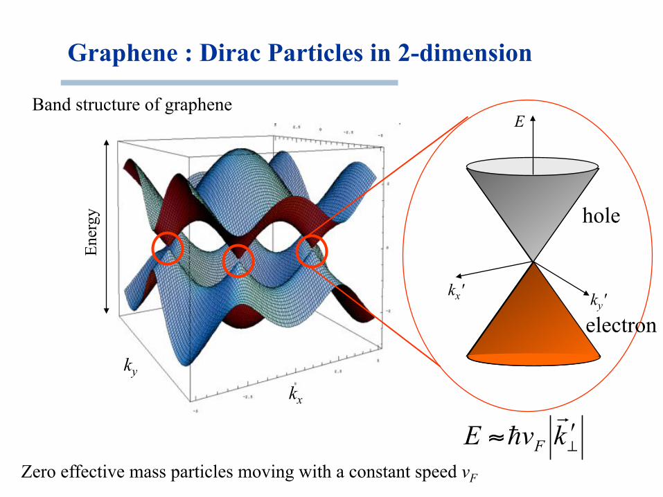
Graphene : Dirac Particles in 2-dimension
Band structure of graphene
kx
ky
Ener
gy
kx' ky'
E
Zero effective mass particles moving with a constant speed vF
hole
electron
- -
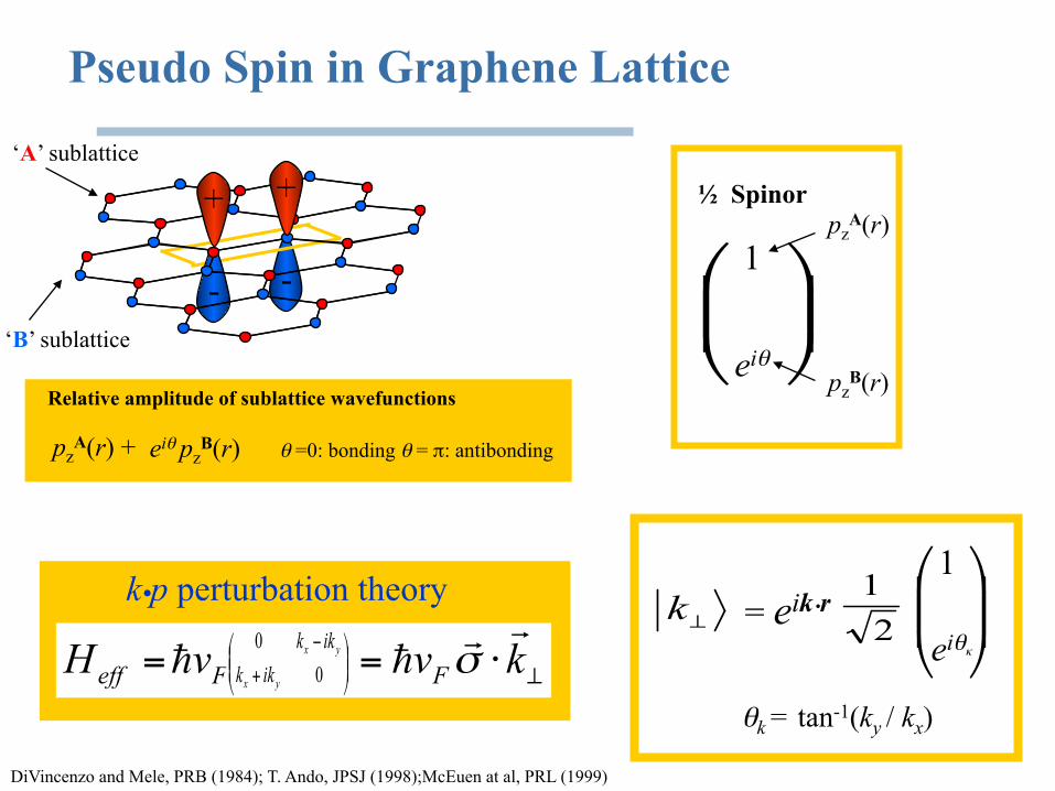
Pseudo Spin in Graphene Lattice
‘A’ sublattice
‘B’ sublattice
+ +
pzA(r) + ei! pz
B(r)
Relative amplitude of sublattice wavefunctions
! =0: bonding ! = !: antibonding
k p perturbation theory .
! Spinor
ei!
1 pz
A(r)
pzB(r)
DiVincenzo and Mele, PRB (1984); T. Ando, JPSJ (1998);McEuen at al, PRL (1999)
!k = tan-1(ky / kx)
= eik r .
ei!"
1
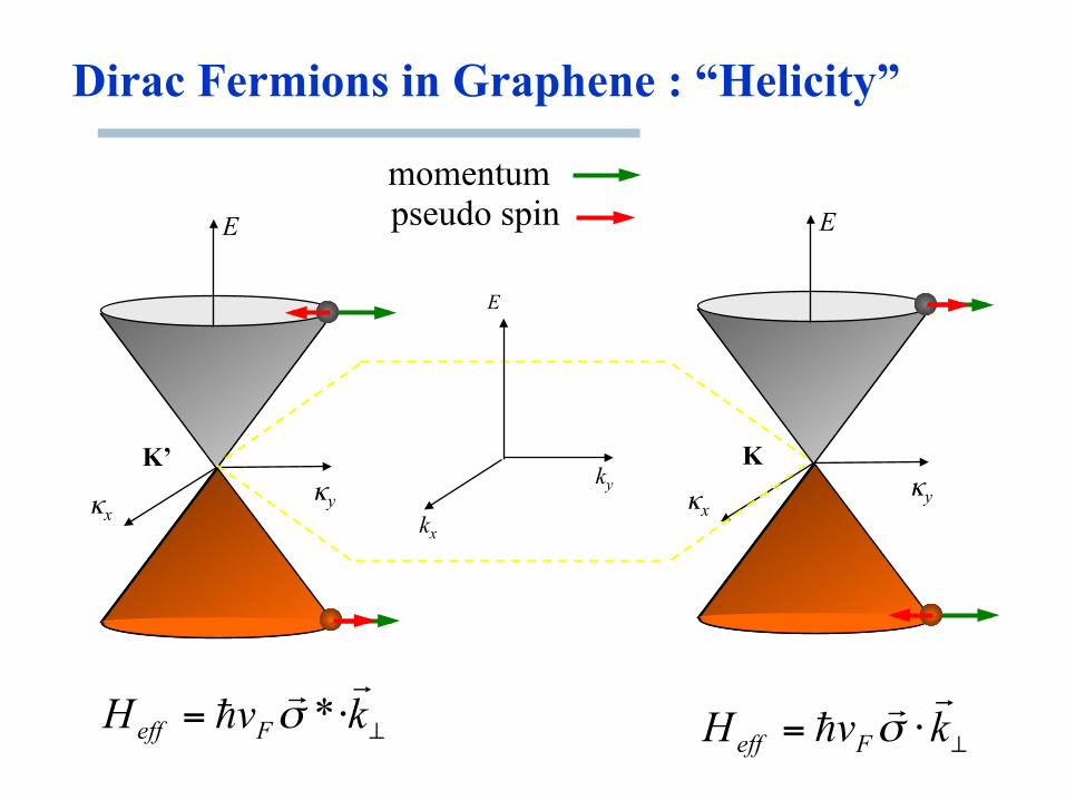
Dirac Fermions in Graphene : “Helicity”
E
"x "y
K
E
"x "y
K’
momentum pseudo spin
E
kx
ky

Single Wall Carbon Nanotube
…. since 1991
Modulate Doped GaAs:
Pfeiffer et al.
Modulate Doped GaAs:
Pfeiffer et al.
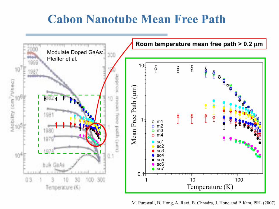
Cabon Nanotube Mean Free Path
M. Purewall, B. Hong, A. Ravi, B. Chnadra, J. Hone and P. Kim, PRL (2007)
Room temperature mean free path > 0.2 µm
Mea
n F
ree
Pat
h (
µm
)
1 10 100 0.1
1
10
Temperature (K)
sc7
sc1 sc2 sc3 sc4 sc5 sc6
m1 m2 m3 m4
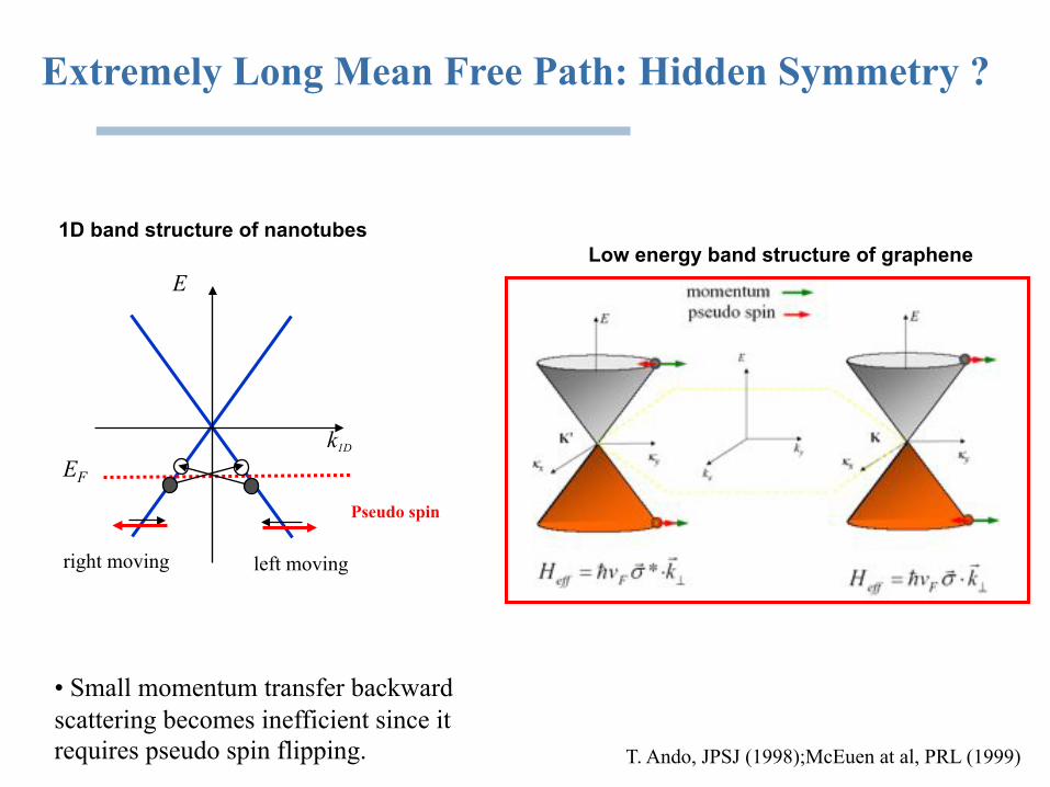
Extremely Long Mean Free Path: Hidden Symmetry ?
E
k1D
EF
right moving left moving
•! Small momentum transfer backward
scattering becomes inefficient since it
requires pseudo spin flipping.
Pseudo spin
T. Ando, JPSJ (1998);McEuen at al, PRL (1999)
Low energy band structure of graphene
1D band structure of nanotubes
Pd (under HfO2)
Pd (under HfO2)
Pd (over HfO2)
SWCNT
(under HfO2)
HfO2 on SiO2/Si+
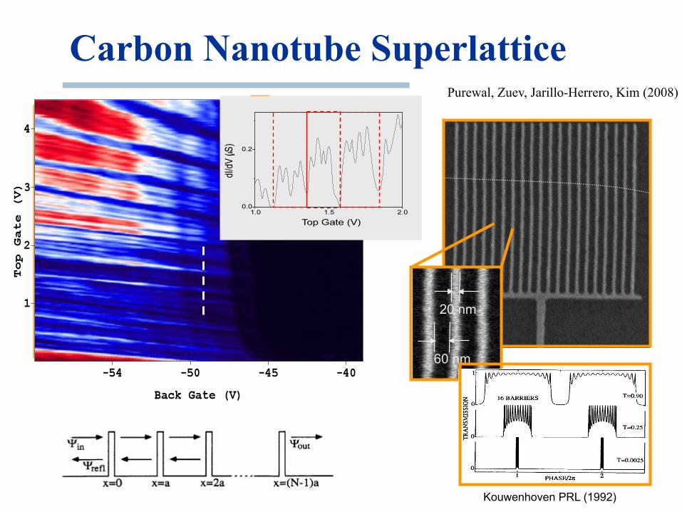
Carbon Nanotube Superlattice
20 nm
60 nm
1 µm
Purewal, Zuev, Jarillo-Herrero, Kim (2008)
Kouwenhoven PRL (1992)

Nanotube Electronics: Challenges
Pros:
High mobility High on-off ratio
High critical current density
Con:
Controlled growth
Artistic dream (DELFT)
IBM, Avouris group
Nanotube Ring Oscillators
graphene
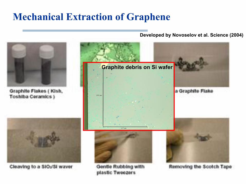
Mechanical Extraction of Graphene
Graphite debris on Si wafer
Developed by Novoselov et al. Science (2004)
1 µm
AFM Image
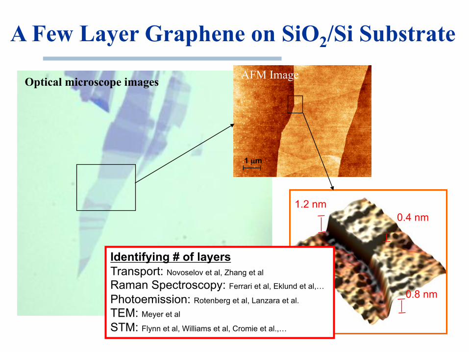
A Few Layer Graphene on SiO2/Si Substrate
0.8 nm
0.4 nm
1.2 nm
Optical microscope images
Identifying # of layers
Transport: Novoselov et al, Zhang et al
Raman Spectroscopy: Ferrari et al, Eklund et al,…
Photoemission: Rotenberg et al, Lanzara et al.
TEM: Meyer et al
STM: Flynn et al, Williams et al, Cromie et al.,…
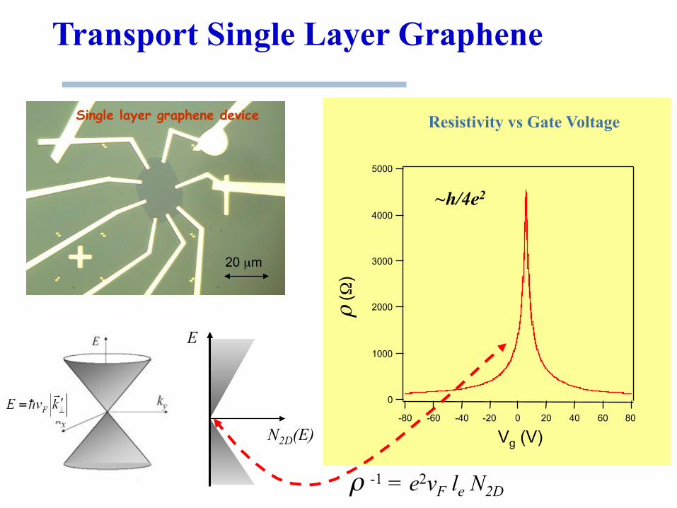
Vg (V)
# ("
)
Resistivity vs Gate Voltage
5000
4000
3000
2000
1000
0 -80 -60 -40 -20 0 20 40 60 80
Transport Single Layer Graphene
Cleaved graphite crystallite 20 µm
Single layer graphene device
~h/4e2
E
N2D(E)
# -1 = e2vF le N2D

15
10
5
0
8 6 4 2 0
6
4
2
0
Hall
Re
sis
tance (
k"
)
Ma
gneto
resis
tance (k"
) B (T)
Quantum Hall Effect in Graphene
__ __ h
e2
1
2
__ __ h
e2
1
6
__ __ h
e2
1
10
T=50 mK
__ __ h
e2
1
2
-15
-10
-5
0
5
10
15
-50 0 50
Vg (V)
Hall
Resis
tance (
k"
)
T= 1.5K, B= 9T
__ __ h
e2
1
6
__ __ h
e2
1
10
__ __ h
e2
1
14
h 1 __ __ e2 -14
e2
__ __ h 1
-10
__ __ h
e2
1
-6
__ __ h
e2
1
-2 Quantization:
4 (n + ) Rxy =
-1 __ _ e
h
2
2 1
Vg=-2 V
Novoselov et al, Zhang et al (2005)
Graphene:
kx' ky'
E
B=0
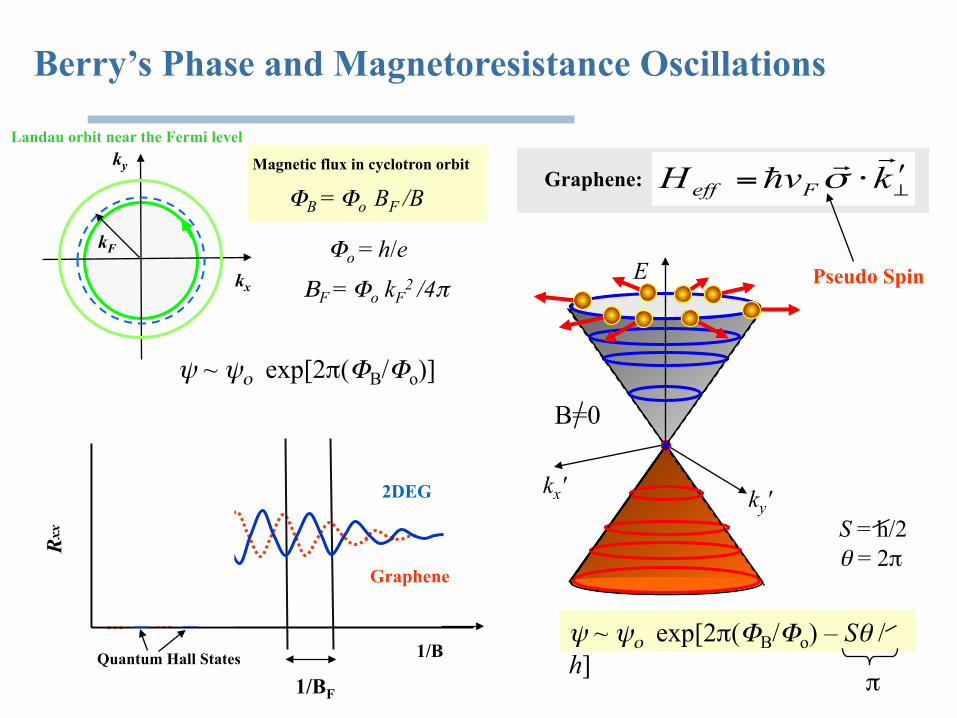
Berry’s Phase and Magnetoresistance Oscillations
Landau orbit near the Fermi level
Pseudo Spin
Graphene
$ ~ $% exp[2!(&B/&o)]
$ ~ $% exp[2!(&B/&o) – S! /
h] !#
kF
S = h/2
! = 2!#
ky
kx
&o = h/e
'F = &o kF2 /4(
#
&B = &o BF /B
Magnetic flux in cyclotron orbit
Rx
x
2DEG
1/BF
1/B Quantum Hall States
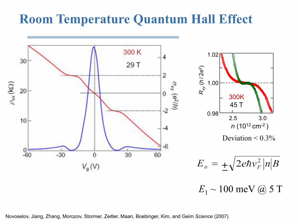
Room Temperature Quantum Hall Effect
+ _
E1 ~ 100 meV @ 5 T
Novoselov, Jiang, Zhang, Morozov, Stormer, Zeitler, Maan, Boebinger, Kim, and Geim Science (2007)
1.02
1.00
0.98 3.0 2.5
n (1012 cm-2 )
Rxy (
h /
2e
2)
300K
45 T
Deviation < 0.3%
Vg (V)
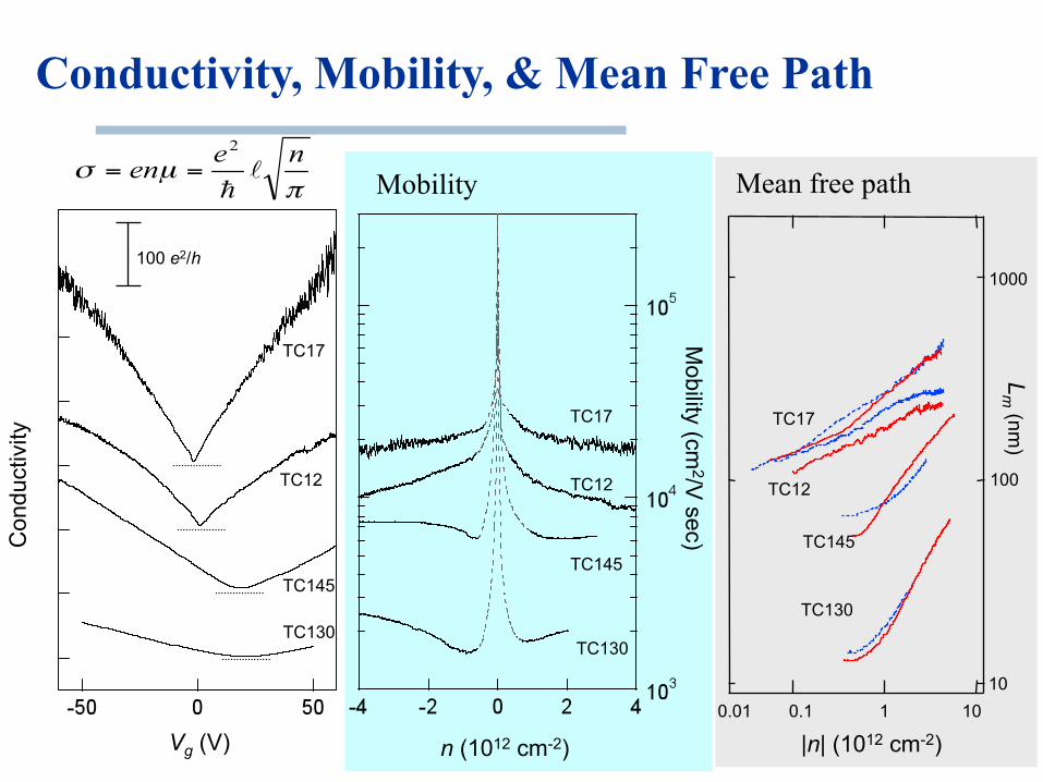
Cond
uctivity
100 e2/h
TC17
TC12
TC145
TC130
Conductivity, Mobility, & Mean Free Path
n (1012 cm-2)
Mobility
(cm
2/V s
ec)
TC17
TC12
TC145
TC130
Mobility
0.01 0.1 1 10
Lm
(nm
)
100
1000
10
TC17
TC12
TC145
TC130
Mean free path
|n| (1012 cm-2)

Graphene Mobility
n (1012 cm-2)
Mobility
(cm
2/V s
ec)
TC17
TC12
TC145
TC130
Graphene Mobility
Modulate Doped GaAs:
Pfeiffer et al.
GaAs HEMT
Tan et al. PLR (2007)

STM on Graphene
Atomic resolution Ripples of graphene on a SiO2 substrate
Elena Polyakova et al (Columbia Groups), PNAS (2007)
Scattering Mechanism?
•!Ripples
•!Substrate (charge trap)
•!Absorption
•!Structural defects See also Meyer et al, Nature (2007) and Ishigami et al, Nano Letters (2007)

Toward High Mobility: Suspending Samples
graphene
HF etching
-> critical pointing drying
SEM image of suspended graphene
AFM image of suspended graphene You should not apply to high gate voltage, otherwise…
Collapsed graphene devices…
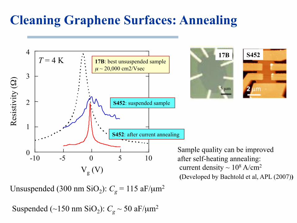
Cleaning Graphene Surfaces: Annealing
0 5 10 -10 -5 0
2
4
3
1
Vg (V)
Res
isti
vit
y ("
)
17B: best unsuspended sample
µ ~ 20,000 cm2/Vsec
S452: suspended sample
S452: after current annealing
Unsuspended (300 nm SiO2): Cg = 115 aF/µm2
Suspended (~150 nm SiO2): Cg ~ 50 aF/µm2
T = 4 K
Sample quality can be improved
after self-heating annealing:
current density ~ 108 A/cm2
(Developed by Bachtold et al, APL (2007))
S452 17B
5 µm
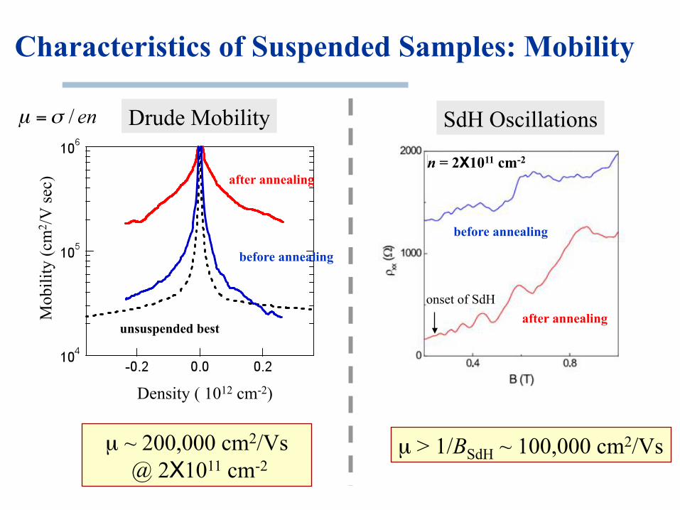
Drude Mobility
unsuspended best
before annealing
after annealing
Density ( 1012 cm-2)
Mobil
ity (
cm2/V
sec
)
µ ~ 200,000 cm2/Vs
@ 2X1011 cm-2
n = 2X1011 cm-2
SdH Oscillations
after annealing
before annealing
onset of SdH
µ! > 1/BSdH ~ 100,000 cm2/Vs
Characteristics of Suspended Samples: Mobility
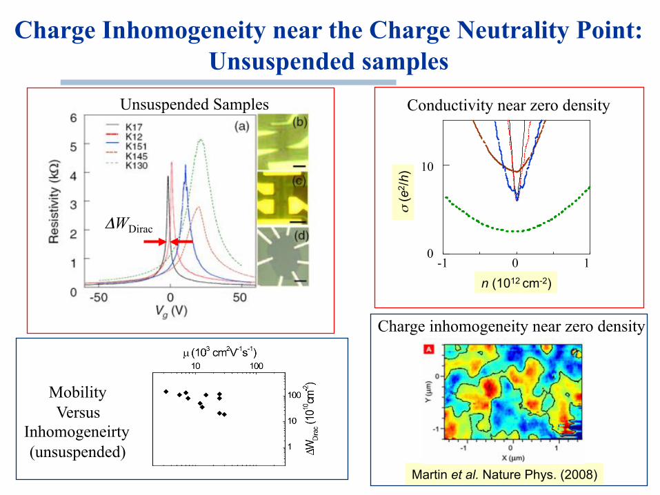
Charge Inhomogeneity near the Charge Neutrality Point:
Unsuspended samples
n (1012 cm-2)
) (
e2/h
)
0 1 -1 0
10
Conductivity near zero density Unsuspended Samples
Martin et al. Nature Phys. (2008)
Charge inhomogeneity near zero density
Mobility
Versus
Inhomogeneirty
(unsuspended)
*WDirac
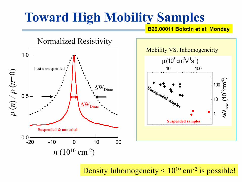
Toward High Mobility Samples
Mobility VS. Inhomogeneirty
Suspended samples
n (1010 cm-2)
# (
n)
/ #
(n=
0)
Normalized Resistivity
$WDirac
$WDirac
Density Inhomogeneity < 1010 cm-2 is possible!
best unsuspended
Suspended & annealed
B29.00011 Bolotin et al: Monday
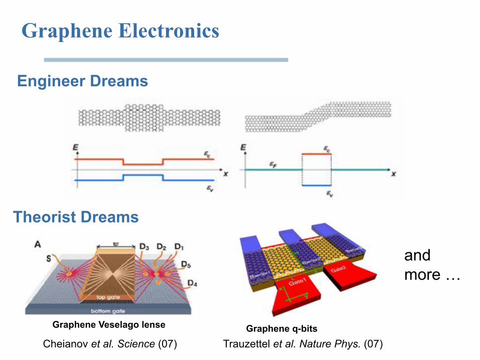
Graphene Electronics
Engineer Dreams
Cheianov et al. Science (07) Trauzettel et al. Nature Phys. (07)
Theorist Dreams
Graphene Veselago lense Graphene q-bits
and
more …
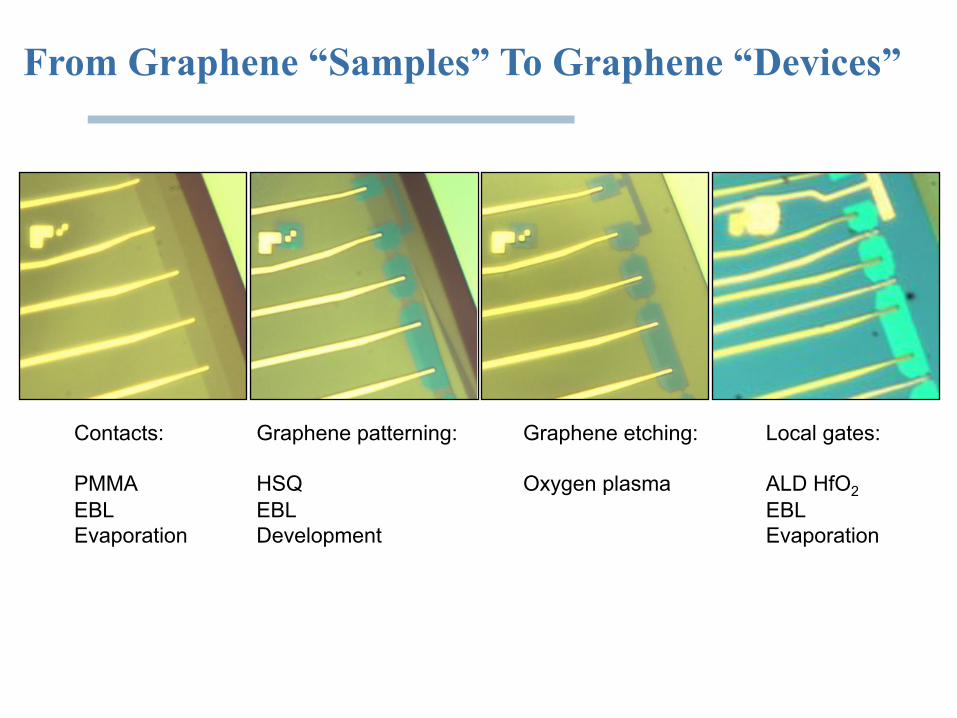
Contacts:
PMMA
EBL
Evaporation
Graphene patterning:
HSQ
EBL
Development
Graphene etching:
Oxygen plasma
Local gates:
ALD HfO2
EBL
Evaporation
From Graphene “Samples” To Graphene “Devices”
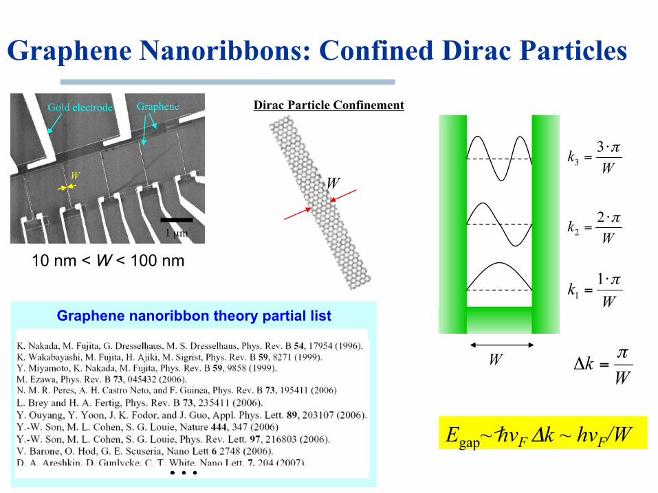
W
Dirac Particle Confinement
Egap~ hvF *k ~ hvF/W
1 µm
Gold electrode Graphene
10 nm < W < 100 nm
W
Zigzag ribbons
Graphene nanoribbon theory partial list
Graphene Nanoribbons: Confined Dirac Particles
W
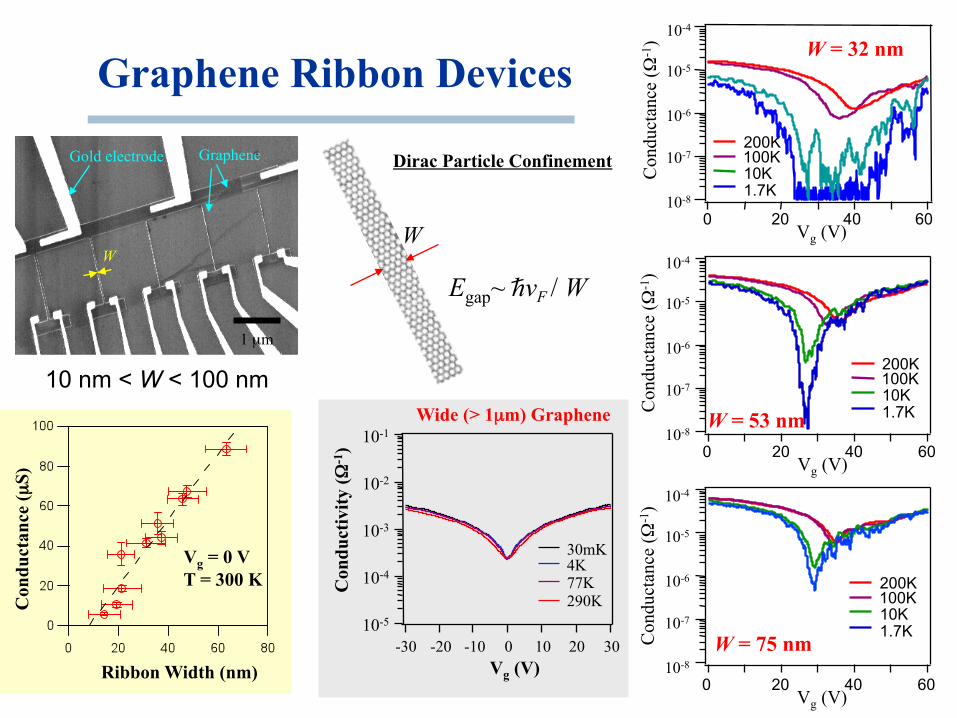
Wide (> 1µm) Graphene
10-5
10-4
10-3
10-2
10-1
-30 -20 -10 0 10 20 30
30mK 4K 77K 290K
Vg (V)
Con
du
ctiv
ity ("
-1)
Graphene Ribbon Devices
W
Dirac Particle Confinement
Egap~ hvF / W
200K 100K 10K 1.7K
10-4
10-5
10-6
10-7
10-8
Conduct
ance
("
-1)
60 40 20 0 Vg (V)
W = 75 nm
200K 100K 10K 1.7K
10-4
10-5
10-6
10-7
10-8
Conduct
ance
("
-1)
60 40 20 0 Vg (V)
W = 53 nm
10-4
10-5
10-6
10-7
10-8
Conduct
ance
("
-1)
60 40 20 0 Vg (V)
200K 100K 10K 1.7K
W = 32 nm
Con
du
ctan
ce (
µS
)
Ribbon Width (nm)
Vg = 0 V
T = 300 K
1 µm
Gold electrode Graphene
10 nm < W < 100 nm
W

Scaling of Energy Gaps in Graphene Nanoribbons
W (nm)
Eg (
meV
)
0 30 60 90 1
10
100
P1 P2 P3 P4 D1 D2
Eg = E0 /(W-W0)
Han, Oezyilmaz, Zhang and Kim PRL (2007)
-8 -4 0 4 8
75
50
25
0
-25
-50
-75
VLG (V)
VB
G (V
)
10-7 10-5 10-3 10-1
G (e2/h) The image cannot be displayed. Your computer may not have enough memory to open the image, or the image may have been corrupted. Restart your computer, and then open the file again. If the red x still appears, you may have to delete the image and then insert it again.
Top Gated Graphene Nano Constriction
source
Back gate
SiO2
drain graphene
Hf-oxide
Top gate
-8 -4 0 4 8
10-6
10-5
10-4
10-3
10-2
10-1
VLG (V)
G (
e2/h
)
OFF
SEM image of device
source drain top gate
graphene
1 µm
30 nm wide x 100 nm long
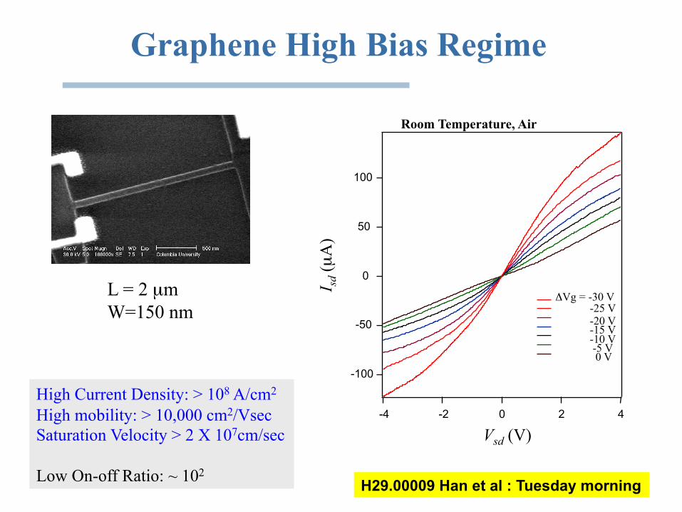
L = 2 µm
W=150 nm
Vsd (V)
I sd (
µA
)
100
50
0
-50
-100
-4 -2 0 2 4
$Vg = -30 V
-20 V -15 V -10 V -5 V 0 V
-25 V
Graphene High Bias Regime
High Current Density: > 108 A/cm2
High mobility: > 10,000 cm2/Vsec
Saturation Velocity > 2 X 107cm/sec
Low On-off Ratio: ~ 102
Room Temperature, Air
H29.00009 Han et al : Tuesday morning
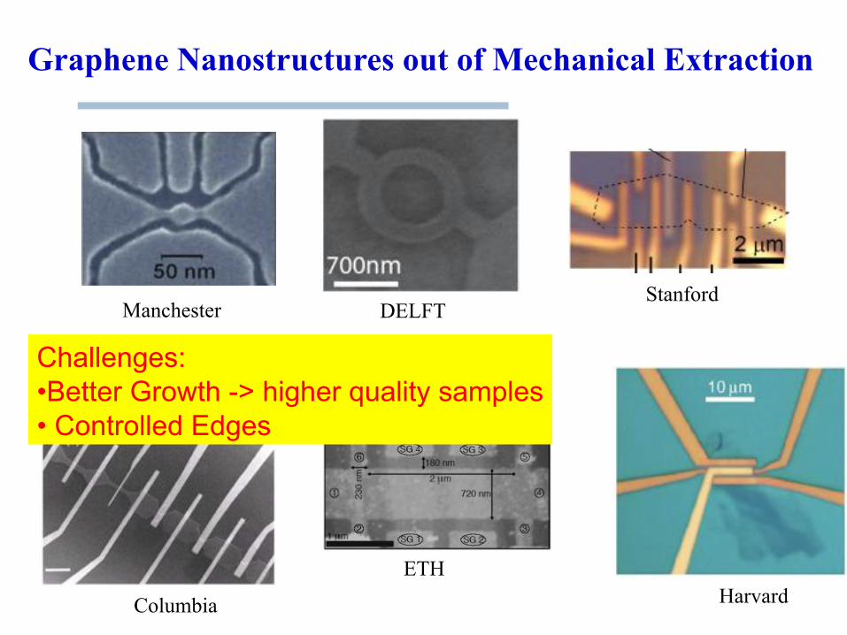
Graphene Nanostructures out of Mechanical Extraction
Manchester DELFT Stanford
Columbia
ETH
Harvard
Challenges:
•!Better Growth -> higher quality samples
•! Controlled Edges
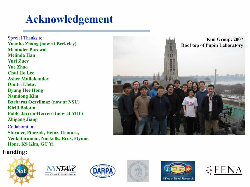
Acknowledgement
Special Thanks to:
Yuanbo Zhang (now at Berkeley)
Meninder Purewal
Melinda Han
Yuri Zuev
Yue Zhao
Chul Ho Lee
Asher Mullokandov
Dmitri Efetov
Byung Hee Hong
Namdong Kim
Barbaros Oezyilmaz (now at NSU)
Kirill Bolotin
Pablo Jarrilo-Herrero (now at MIT)
Zhigang Jiang
Funding:
Collaboration:
Stormer, Pinczuk, Heinz, Uemura,
Venkataraman, Nuckolls, Brus, Flynne,
Hone, KS Kim, GC Yi
Kim Group: 2007
Roof top of Pupin Laboratory


![Optically driven oscillations of ellipsoidal particles ... · particles such as nanowires, nanotubes, graphene or quan-tum dots [16,17,30,31]. The outline of the paper is as follows:](https://img.pdfslide.us/doc/110x75/5f0e690e7e708231d43f1c94/optically-driven-oscillations-of-ellipsoidal-particles-particles-such-as-nanowires.jpg)