Embed Size (px)
Citation preview
1
PHYSICS OF ELECTRO-OPTIC DETECTORS
copyright 1998-2014 Everett Companies LLC
INTRODUCTION
An electro-optic detector absorbs electromagnetic radiation and outputs an electrical signal that is usually proportional to the irradiance (intensity of the incident electromagnetic radiation). Depending on the type of detector and the way in which it is operated, the output signal can be either a voltage or a current.
An electro-optic sensor consists of the detector, the optics needed to focus the incident radiation on the detector and the electronics that captures the detector signal, amplifies it and presents it to an interface where it can operate a switch or perform whatever task is appropriate. Such a sensor is a motion sensor that detects the approach of a person, car or other object and turns on the lights mounted on the corners of a garage. Another example is the X-ray camera that dentists now use to X-ray a person's teeth. The camera consists of a mega-pixel array of silicon carbide photodiodes that capture the X-rays that pass through the person's teeth and convert the photodiode signals to a high resolution image that is stored on a computer hard drive. The photodiodes are so sensitive that the radiation intensity and exposure duration are a very small fraction of that required for the old X-ray film. Also, a chemical developing process is not required. Today's still and video cameras are very similar except that an array of silicon rather than silicon carbide detectors is used. We will be concerned here with the interaction between the detector and the incident electro-magnetic radiation and to some degree the optics but not with the electronics that takes the detector signal and turns it into something useful. The accompanying article Preamplifiers for Electro-optic Detectors gives an introduction to the first stage of these electronics.
All objects at any finite temperature emit electromagnetic radiation. When this radiation is detected it is called passive detection. We also have active sources of radiation. These are sources that emit radiation not just due to their finite temperatures but to an applied energy source such as an electric current. These sources can be anything from a light bulb to a laser to an LED or an X-ray generator.
2
The light bulb filament is emitting radiation because an electric current is heating the filament to an elevated temperature, but we consider this an active source since we can turn the current on and off. Here we will just consider passive sources of radiation. The extension to active sources should be fairly clear. We just have to know what radiation the source is emitting.
In order to get started we will first discuss the properties of electromagnetic radiation.
ELECTROMAGNETIC RADIATION
The electromagnetic spectrum is rather arbitrarily divided into regions. The spectral region to which the human eye is sensitive is referred to as visible. It extends from wavelengths of about 400 nm to about 700 nm. Wavelengths shorter than visible are successively referred to as ultraviolet, x-rays and gamma rays. The infrared region is considered to extend from 700 nm to 1000 µm. Wavelengths longer than 1 mm are referred to as radio waves. There are no consistent definitions of the various infrared spectral bands, but the region from 700 nm to 1 µm is usually called the near infrared or NIR. The infrared region is further subdivided into short wave infrared or SWIR (1-3 µm), mid-wave infrared or MWIR (3-6 µm) and long wave infrared or LWIR (>6 µm). However, the MWIR region is often considered to be 3-5 µm and LWIR 8 µm and longer. The reason is that the atmosphere absorbs radiation strongly in the 5-8 µm band, and these wavelengths are seldom used.
Electromagnetic radiation has been understood since the time of Maxwell. An electromagnetic wave is emitted whenever an electrical charge is accelerated. Since matter is largely composed of electrically charged particles that are constantly in motion, electromagnetic radiation is continuously emitted by all objects. The intensity and spectral distribution of the radiation depend to a large degree on the temperature of the object. The higher the temperature the more vigorously the electrons in the material bounce around, the more they are accelerated and the more radiation they emit. Maxwell, however, did have a problem since the spectral density of the radiation predicted by his theory kept increasing with decreasing wavelength becoming infinite at zero wavelength. Since this would require an infinite source of energy, it did cause some conceptual problems, and the issue was referred to as the ultraviolet catastrophe. Observation, however, showed that there really was no catastrophe. The experimentally measured spectral density increased with decreasing wavelength as Maxwell predicted but then peaked and decreased toward zero at shorter wavelengths. The question then was why, and Max Planck, who came along not too much after Maxwell, came up with what he thought was a mathematical manipulation to solve the problem. He postulated that the energy was not really emitted as continuous waves as Maxwell had assumed but rather as little chunks called quanta. These quanta are actually little wave packets, and a bunch of them can add up to make a pretty good wave. This solved the problem, and Planck's theory fit the observations nearly perfectly. This, of
3
course, is the foundation on which modern physics and quantum mechanics are based. Planck, however, was a true classicist and never felt that his quanta were anything more than a mathematical device, rejecting the implications of his fundamental discovery.
Emitted Radiation
In any case, the spectral distribution of the radiation emitted by a perfect emitter or radiator (called a blackbody) is given by what is now known as Planck's Law
( ) 1/5212
−− −= kTchehcW
λλ λπ
where
h is Planck's constant (6.626x10⁻³⁴ Js) c is the speed of light (2.9979x10⁸ m/s)
k is Boltzmann's constant (1.381x10⁻²³ J/K) λ is the wavelength in m
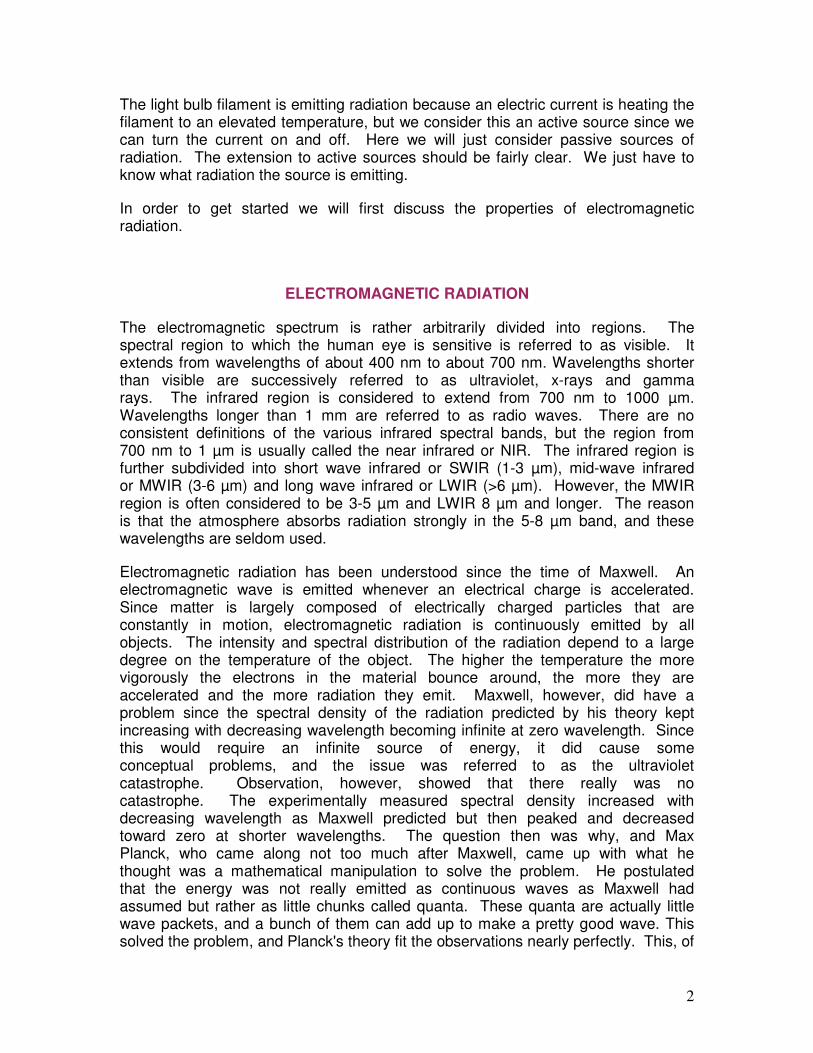
T is the absolute temperature in K The spectral radiant emittance, Wλ, is the optical power radiated into a hemisphere per unit area of emitting surface per unit wavelength and is shown in Figure 1 for a blackbody at room temperature (20o C). The term optical is being used here to refer to the entire electromagnetic spectrum of interest from ultraviolet through visible to infrared.
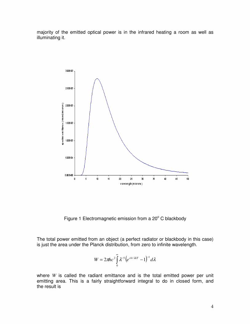
The unit of spectral radiant emittance is power per unit area per unit wavelength. While it would be appropriate to use standard SI units throughout, we will follow standard usage and give wavelengths in microns (µm) and areas in cm2. It is the reader's responsibility to keep the numbers straight. The emitted power distribution in Figure 1 peaks at about 10 µm and falls fairly rapidly toward zero for shorter wavelengths. Nearly all of the electromagnetic emission from an object at a typical room temperature is in the infrared portion of the spectrum. As the temperature is increased the emission increases at all wavelengths, but it increases faster at shorter wavelengths causing the peak of the distribution to shift toward shorter wavelengths. This is illustrated in Figure 2.
We know that as an object is heated it starts to glow, first red hot and finally white hot as the temperature increases. As the object is heated the distribution peak shifts to shorter wavelengths and the short wavelength tail starts to be pulled up. The emission at the long wavelength end of the visible spectrum, around 0.7 µm, rises to observable levels first, and the object appears to be red. As the temperature is raised further emission over the entire visible spectrum becomes significant, and the color moves from red toward white. However, even at rather high temperatures the distribution peak is still in the infrared. An incandescent light bulb casts a "warm" light that is weighted toward the red end of the spectrum, but the
4
majority of the emitted optical power is in the infrared heating a room as well as illuminating it.
Figure 1 Electromagnetic emission from a 20o C blackbody
The total power emitted from an object (a perfect radiator or blackbody in this case) is just the area under the Planck distribution, from zero to infinite wavelength.
( )∫∞
−− −=0
1/5212 λλπ λ
dehcWkTch
where W is called the radiant emittance and is the total emitted power per unit emitting area. This is a fairly straightforward integral to do in closed form, and the result is
5
Figure 2 Electromagnetic emission from 100 oC and 1000 oC blackbodies
44
32
45
15
2TT
hc
kW σ
π==
where σ = 5.6697x10⁻¹² Wcm-2K-4. This is known as the Stefan-Boltzmann Law, and σ is usually called Stefan's constant. The problem with the Stefan- Boltzmann Law is that it is hardly ever useful. The reason is that it includes all wavelengths. The law accurately represents the total optical power emitted by a blackbody. However, it does not represent the optical power that reaches a detector or other object. This is because there is almost always something in the optical path that passes some wavelengths and absorbs or reflects others, such as the window on a detector package or a spectral filter. The atmosphere is a classic example where there is very strong absorption in the 5-8 µm region due primarily to the presence of water molecules. The Stefan-Boltzmann Law must
6
be used only with great care, and it is almost always the case that the Planck equation must be numerically integrated after inserting the appropriate spectral transmission function.
The emission from most real objects is similar to that from a blackbody except the Planck equation is more or less scaled by a parameter called the emissivity, ε. The emissivity of a perfect radiator or blackbody is ε = 1, and the emissivity of a perfect reflector is ε = 0. This is a valid concept within the realm of classical physics, but we run into trouble when quantum mechanics becomes involved. For example, the electrons in a piece of material are not free to emit radiation at any and all wavelengths as is assumed in classical electrodynamics but only those wavelengths that correspond to transitions between the electron's discrete energy levels. We will carry this discussion a bit further below. The effect of this is to introduce some deviations to the spectral distributions of the radiation from real objects from the purely Planck distribution. These deviations can be accounted for by absorbing them into the emissivity thereby making it a function of wavelength and temperature. However, in most situations the deviations are small enough to be ignored, and we will consider the emissivity to be a simple number independent of both wavelength and temperature. We find this to be a valid approach in nearly all situations, particularly in the infrared region. For example, the emission from a light bulb looks very much like the Planck distribution for an object at the temperature of the filament.
Then for a real emitting surface
( ) 1/5212
−− −= kTchehcW
λλ λπε
The total optical power emitted per unit surface area then is
( )∫∞
−− −=0
1/5212 λλπε λ
dehcWkTch
where T is the temperature of the emitting surface.
Most surfaces emit the radiation uniformly over a hemisphere in front of the emitting surface element, and such emission is referred to as Lambertian. It makes for an interesting calculus problem if the emitting surface is not flat. However, in the case of a flat surface it is straightforward to determine the amount of radiation captured by an aperture. The fraction of the total emitted radiation that is incident on the aperture is just the solid angle subtended by the
aperture divided by the solid angle of a hemisphere which is 2π steradians.
Radiation at specific wavelengths or within relatively narrow spectral bands can be generated electrically. Short wavelength radiation such as x-rays can be preferentially generated by accelerating electrons to high energy and having them rapidly decelerate by striking a target. Light emitting and laser diodes emit radiation at particular wavelengths by causing electron transitions between the
7
conduction and valence bands of the diode's semiconducting material. These phenomena are not described by Planck's Law but rather by quantum mechanics.
Reflected Radiation
The radiation emanating from a surface includes not only that emitted by the surface but also that reflected by the surface. The objects surrounding the surface in question also emit radiation in spectral distributions appropriate to their respective temperatures. This radiation, or at least some portion of it, is incident on our surface of interest where it is partially absorbed and partially reflected. To an observer the reflected radiation is indistinguishable from the emitted radiation.
We will consider our radiating object of interest to be opaque. This means that the incident radiation at any wavelength is either absorbed or reflected. We know that the reflectivities of the surfaces of most objects can have strong spectral dependencies, particularly at the shorter wavelengths. That is why one object appears to be red while other objects are blue, green or any other color. This results from the absorption of quanta of radiation at specific wavelengths resulting in the excitation of the object's electrons from one energy level to another. In other words this is a quantum mechanical effect. Since we are limiting our considerations to the classical realm, we can ignore any spectral dependencies and say
1=+ ra
where
a is the spectral absorption coefficient r is the spectral reflection coefficient
and a and r are independent of wavelength
After all, the incident energy is either absorbed or reflected.
We will consider an object at temperature T that is in thermal equilibrium with all of its surrounding objects which then are also at temperature T. Since everything is in thermal equilibrium whatever radiation is absorbed must be re-emitted at the same rate. Also, the incident and emitted radiation have the same spectral distribution since they correspond to the same temperature. Then conservation of energy tells us that
ε=a
and
1=+ rε
8
As mentioned above ε = 1 for a blackbody, and, therefore, r = 0. The perfect radiator absorbs everything and reflects nothing. On the other hand, the perfect reflector, with r = 1, reflects everything and absorbs nothing.
The emitted radiation and the reflected radiation from the object under consideration must have the same spectral distribution since they were emitted from objects at the same temperature. The emitted and reflected radiation then simply add to give the blackbody radiation, equivalent to that from a surface with unity emissivity and zero reflectivity. This leads us to the simple idea that the radiation within an enclosure where everything in the enclosed space including the enclosure walls are at the same temperature is identical to the radiation coming from a blackbody at that temperature. In fact, this is the best known method to approximate true blackbody radiation. A hollow sphere with a small "pin hole" is brought to a known uniform temperature. The radiation exiting the pin hole is the blackbody radiation corresponding to that temperature.
We usually refer to the object or surface of interest as the target. The objects surrounding the target are normally referred to as the background. However, since we are considering reflected radiation, foreground might be a more appropriate term, but we will stick with convention. It is frequently the case that the objects in the background are at a more or less uniform temperature that we will call Ta for ambient temperature. If this is not the case, we have to take into account the individual temperature of each object in the background, a laborious if not difficult task. If we assume that the surrounding objects are all at temperature Ta, the radiation incident on our target is the blackbody radiation field corresponding to Ta, assuming that the target is small enough that it does not disrupt the radiation field. The radiation reflected from the target per unit area of reflecting surface then is
( ) ( )∫∞
−− −−=0
1/52112 λλεπ λ
dehcW akTch
r
The total radiation per unit emitting area coming from our target object, Wtot, is the
sum of the emitted and reflected components.
( ) ( ) ( )∫ ∫∞ ∞
−−−− −−+−=+=0 0
1/521/5211212 λλεπλλπε λλ
dehcdehcWWW at kTchkTch
retot
where the spectral distribution of the emitted radiation corresponds to the target temperature Tt and the reflected radiation corresponds to the background temperature Ta.
We need to be a little bit careful here. Wtot given above is the total optical power per unit area coming from the target object's surface. It is often the change in optical power between when the object is present and when it is not present that is of interest to us. When the object is not present we just see the
9
blackbody radiation corresponding to Ta coming from this element of solid angle. Then the difference between the target object being present and absent is
( ) ( )
−−=∆ ∫ ∫
∞ ∞−−−−−
0 0
11/51/5212 λλλλεπ λλ
dedehcW at kTchkTch
tot
For the moment we will continue dealing with the total emitted and reflected radiation from the target, Wtot rather than ∆Wtot, since that makes it a bit easier conceptually to keep things straight. However, we will revert to ∆Wtot when it is appropriate.
Radiation Reaching a Detector
Now we have to ask the question, how much radiation emitted by all sources reaches our detector. To keep things simple we will consider only planar detectors, detectors that have a single flat surface that is sensitive to the incident radiation. This is not always the case. We could, for example, have a spherical detector and sometimes do. However, most of the time the detector is indeed planar, and such detectors have hemispherical fields-of-view. Light, as they say, travels in a straight line. Some portion of the radiation emanating from the surface of an object with an unimpeded view of the detector's optically sensitive surface will reach that surface and be detected. All such objects must lie in the volume in front of the detector since any object behind the detector has no view of the detector's front surface at all. While we only need to consider the front half when we are considering emission, we cannot ignore the objects behind the detector when it comes to reflected radiation.
Image of the Target Focused onto the Detector
The above expression for Wtot gives the amount of optical power emitted and reflected per unit surface area (usually given in units of W/cm2). We are considering only diffuse or Lambertian emitting surfaces so the radiation is uniformly distributed over the hemisphere in front of this surface. We typically set up an optical system with a lens that captures some fraction of this radiation and directs it onto a detector. We will first consider the situation where we adjust the lens-to-detector distance so that an image of the emitting surface is focused on the detector. This is illustrated in Figure 3.
10
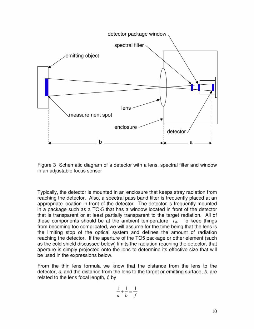
Figure 3 Schematic diagram of a detector with a lens, spectral filter and window in an adjustable focus sensor
Typically, the detector is mounted in an enclosure that keeps stray radiation from reaching the detector. Also, a spectral pass band filter is frequently placed at an appropriate location in front of the detector. The detector is frequently mounted in a package such as a TO-5 that has a window located in front of the detector that is transparent or at least partially transparent to the target radiation. All of these components should be at the ambient temperature, Ta. To keep things from becoming too complicated, we will assume for the time being that the lens is the limiting stop of the optical system and defines the amount of radiation reaching the detector. If the aperture of the TO5 package or other element (such as the cold shield discussed below) limits the radiation reaching the detector, that aperture is simply projected onto the lens to determine its effective size that will be used in the expressions below.
From the thin lens formula we know that the distance from the lens to the detector, a, and the distance from the lens to the target or emitting surface, b, are related to the lens focal length, f, by
fba
111=+
a b
detector
detector package window
enclosure
lens
emitting object
measurement spot
spectral filter
11
Also, simple proportion tells us that the area of the emitting surface that is focused onto the detector, At, is related to the size of the detector, Ad, by
dt Aa
bA
2
2
=
Since the radiation is spread uniformly over the hemisphere in front of the target, the fraction of the emitted and reflected radiation captured by the lens and focused onto the detector is the ratio of the solid angle subtended by the lens as seen from the target surface to the 2π solid angle of a hemisphere. This fraction, F, is then given by
22 b
AF l
π=
where
Al is the cross sectional area of the lens
The numerator in the above expression is actually the area of the hemisphere of radius b that is intercepted by the lens rather than the lens cross section. However, the difference is usually small enough that it can be neglected. We have assumed that the lens is the limiting stop in the optical train. If not, Al
should be replaced with the area of the limiting stop projected onto the lens.
Notice that At increases as b2 while the fraction of the radiation emitted by this
surface and captured by the lens decreases as b-2. The two cancel, and the
amount of radiation from the target reaching the detector is independent of the distance to the target. This is the case as long as everything is kept in focus, and the size of the spot that is focused onto the detector does not spill over the edges of the target surface.
This radiation must pass through the lens, filter and window, if present, before it reaches the detector. Each of these components will have spectral transmission functions that will vary with wavelength, particularly the filter, and this transmission or lack of it must be taken into account. Then the amount of optical power from the target that reaches the detector is
( ) ( )∫∞
−− −==0
1/5
2
2
1 λλλε λdet
a
AAhcFAWP tkTchdl
ttott
( ) ( ) ( )∫∞
−− −−+0
1/5
2
2
11 λλλε λdet
a
AAhcakTchdl
where
12
( ) ( ) ( ) ( )λλλλ wfl tttt =
and
tl(λ) is the spectral transmission function of the lens tf(λ) is the spectral transmission function of the filter
tw(λ) is the spectral transmission function of the window on the detector package
If there are other components in the optical path, their transmission functions are simply included in the product for the net spectral transmission function. The above expression tells us how much optical power is incident on the detector that was emitted by the target and that emitted by the background and reflected by the target.
If the target were not present, the radiation reaching the detector coming from the element of solid angle that would have been occupied by the target is just the blackbody radiation corresponding to Ta, and the difference in the amount of optical power reaching the detector when the target is present and not present is
( ) ( ) ( ) ( )
−−−=∆ ∫ ∫
∞ ∞−−−−
0 0
1/51/5
2
2
11 λλλλλλε λλdetdet
a
AAhcP at kTchkTchdl
t
In addition, the walls of the detector package or housing also emit radiation that reaches the detector and must be included in our considerations. Often the detector and its housing are at the ambient temperature. However, detectors used for the detection of long wavelength radiation are often cooled to temperatures well below 100 K along with the material comprising the detector's immediate surroundings. We will look at these two situations individually since the housing emitted radiation is handled differently in the two cases.
For ambient or room temperature operation the enclosure often is a TO5 or other standard package on which the window is mounted. Frequently, the window and filter are combined into a single element. The detector and its surrounding material are normally at the ambient temperature Ta. If the enclosure were totally without a window to let outside radiation in and inside radiation out, the radiation field inside the housing would just be the blackbody field corresponding to temperature Ta. In this case, the blackbody radiation incident on the detector would be
( )∫∞
−− −=0
1/5212 λλπ λ
deAhcP akTch
dbb
It is not hard to see where this expression comes from. For the moment assume that Ad is facing a hemisphere at temperature Ta. We are assuming that the material behind the detector is also at temperature Ta. From our above
13
discussion we know that the sum of the emitted and reflected radiation from each element if the hemisphere is just the blackbody radiation corresponding to Ta.
Since we have no lens in this case, Ad is the limiting aperture, so to speak. The amount of optical power reaching the detector from each element of the hemisphere is
( )∫∞
−− −=0
1/52
21 λλδδ λ
dehcR
AAP akTchd
hh
where R is the radius of the hemisphere and δAh is the area of the emitting element. Now we need to add the contributions from all of the elements that make up the hemisphere. Since all of the elements are at the same distance R from the detector, this is fairly straightforward.
( )∫∞
−− −Σ=0
1/52
21 λλδ λ
dehcR
AAP akTchd
hbb
Since ΣδAh = 2πR2, the area of the hemisphere, the equation for Pbb is just that
given above. In the real world we usually do not have a hemispherical enclosure around the detector. In this case we need to treat each element of the enclosure separately with its value of R and the corresponding solid angle subtended by the detector. Suffice it to say that the result is the same.
Pbb is the optical power reaching the detector when the target is not present and everything surrounding the detector is at the ambient temperature. ∆Pt is the change in the optical power reaching the detector when the target is present. Then the total amount of power incident on the detector when the target is present is
( )∫∞
−− −=∆+=0
1/5212 λλπ λ
deAhcPPP akTch
dtbbd
( ) ( ) ( ) ( )
−−−+
−−∞ ∞
−−
∫ ∫ λλλλλλε λλdetdet
a
AAhcat kTchkTchdl 1/5
0 0
1/5
2
2
11
When we use a mechanical chopper we are usually just interested in the difference in the detector signal when the chopper is open and when it is closed, the ac signal from the detector. In this case we drop the dc blackbody term and just use the expression for ∆Pt.
Cryogenically cooled detectors are almost always enclosed by a cold shield at or near the cryogenic temperature. The purpose of the cold shield is to replace the rather large amount of radiation that is coming from enclosure walls at the ambient temperature with the much smaller amount of radiation coming from
14
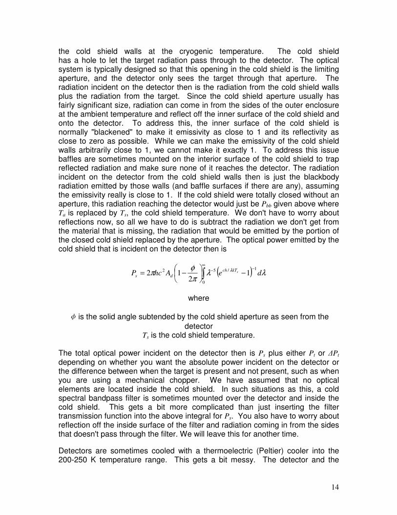
the cold shield walls at the cryogenic temperature. The cold shield has a hole to let the target radiation pass through to the detector. The optical system is typically designed so that this opening in the cold shield is the limiting aperture, and the detector only sees the target through that aperture. The radiation incident on the detector then is the radiation from the cold shield walls plus the radiation from the target. Since the cold shield aperture usually has fairly significant size, radiation can come in from the sides of the outer enclosure at the ambient temperature and reflect off the inner surface of the cold shield and onto the detector. To address this, the inner surface of the cold shield is normally "blackened" to make it emissivity as close to 1 and its reflectivity as close to zero as possible. While we can make the emissivity of the cold shield walls arbitrarily close to 1, we cannot make it exactly 1. To address this issue baffles are sometimes mounted on the interior surface of the cold shield to trap reflected radiation and make sure none of it reaches the detector. The radiation incident on the detector from the cold shield walls then is just the blackbody radiation emitted by those walls (and baffle surfaces if there are any), assuming the emissivity really is close to 1. If the cold shield were totally closed without an aperture, this radiation reaching the detector would just be Pbb given above where Ta is replaced by Ts, the cold shield temperature. We don't have to worry about reflections now, so all we have to do is subtract the radiation we don't get from the material that is missing, the radiation that would be emitted by the portion of the closed cold shield replaced by the aperture. The optical power emitted by the cold shield that is incident on the detector then is
( )∫∞
−− −
−=
0
1/521
212 λλ
π
φπ λ
deAhcP skTch
ds
where
φ is the solid angle subtended by the cold shield aperture as seen from the
detector Ts is the cold shield temperature.
The total optical power incident on the detector then is Ps plus either Pt or ∆Pt depending on whether you want the absolute power incident on the detector or the difference between when the target is present and not present, such as when you are using a mechanical chopper. We have assumed that no optical elements are located inside the cold shield. In such situations as this, a cold spectral bandpass filter is sometimes mounted over the detector and inside the cold shield. This gets a bit more complicated than just inserting the filter transmission function into the above integral for Ps. You also have to worry about reflection off the inside surface of the filter and radiation coming in from the sides that doesn't pass through the filter. We will leave this for another time.
Detectors are sometimes cooled with a thermoelectric (Peltier) cooler into the 200-250 K temperature range. This gets a bit messy. The detector and the
15
cooler surface on which it is mounted are at the lower temperature while the other surroundings are at the ambient temperature. While the cold elements disrupt the ambient black body radiation, the disruption is usually small enough that it can be ignored, and the equations above for an ambient temperature enclosure can be used
Fixed Focus
Frequently, we do not want to be bothered adjusting the focus every time we make a measurement. In this case we can place the detector at the focal point of the lens a distance f behind the lens. This is illustrated in Figure 4. In effect then we have focused the sensor to infinity. The image of the target "focused" onto the detector will be relatively sharp when the distance to the target is large but fuzzy when this distance is small.
Figure 4 Ray trace of emitted radiation reaching a detector placed at the lens focal point. The enclosure with the filter and window are not shown
The lens is assumed to define the aperture. The target is located a distance b in front of the lens, and the image of the target is focused onto the image plane a distance a behind the lens. The detector is placed a distance f, the focal length, behind the lens. All of the radiation emitted by the central violet region of the emitting surface and captured by the lens is intercepted by the detector. However, the same is not true of the green ring or frame that surrounds the central region. Only a fraction of the radiation emitted from this outer region and incident on the lens is focused onto the detector. This fraction decreases from 100% at the inner perimeter of the green ring to zero at the outside edge. As b
b a
f
image plane
detector
target
16
increases, a decreases, and the image plane moves closer to the focal point located a distance f behind the lens. Also, the violet rays shown in Figure 4 move closer to the optical axis at the center, and the green rays move closer to the violet rays until they become identical when b reaches ∞ where the violet and green rays overlap. As b increases the fraction of the radiation from the target that is focused onto the detector from the green ring gets smaller and smaller until it is negligible. As b increases the dimension of the target spot focused onto the detector increases linearly, and the area of the emitting spot increases as b2. Since the size of the lens does not change, the fraction of the hemispherical solid angle subtended by the lens decreases as b
2, and the amount of radiation reaching the detector is independent of b for large target distances as long as the emitting spot projected onto the target is not larger than the target itself. The housing emitted radiation is not affected by whether the sensor has variable or fixed focus or no lens at all and needs to be included in all cases.
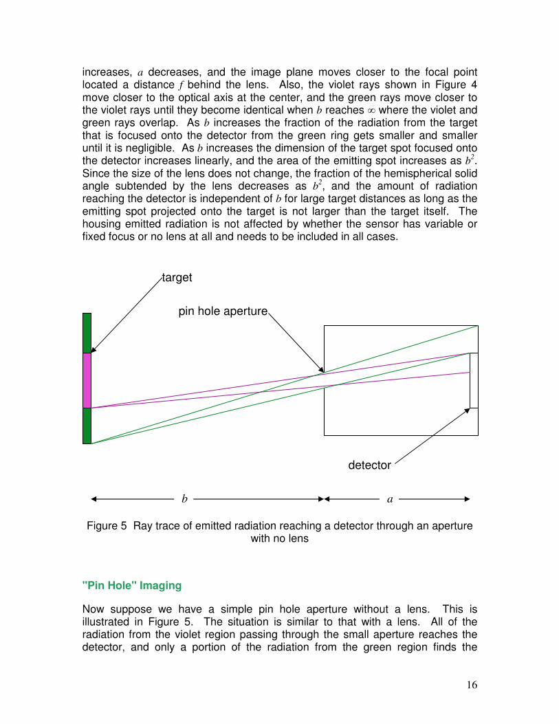
Figure 5 Ray trace of emitted radiation reaching a detector through an aperture with no lens
"Pin Hole" Imaging
Now suppose we have a simple pin hole aperture without a lens. This is illustrated in Figure 5. The situation is similar to that with a lens. All of the radiation from the violet region passing through the small aperture reaches the detector, and only a portion of the radiation from the green region finds the
pin hole aperture
detector
target
b a
17
detector. Assuming the diameter of the aperture is much smaller than b (it is, after all, a pinhole), the area of the violet region increases a b2, and the radiation from it reaching the detector is independent of the distance to the target. However the area of the green ring also increases as b2
, and the radiation from it reaching the detector does not become negligible as b increases. However, the good part is that while the integration over the green region must be done for each detector/enclosure configuration, it only has to be done the one time for all target distances.
How Far Is Enough
The integration required to relate the electromagnetic power incident on a detector to the temperature of the emitting object goes from zero wavelength to infinity. This integration is hardly ever done in any sort of closed form and is almost always done numerically on a computer. Infinity is a long way, and the question is how far do you have to carry the integration to get reasonably good results. The answer depends on temperature as well as the spectral transmission of the optical components and the accuracy with which you need to make the calculation. To get some idea of the temperature dependence we will set spectral transmission aside for the moment and do the integration with all of the spectral transmission functions set to unity. If the temperature of the emitting surface is 1000 K and we integrate from 0-100 µm, we will get all but 0.01% of the emitted power, accurate enough for most applications. However, if the temperature is 300 K, right around typical room temperature, we come up 0.5% short. If the temperature is 100 K, a bit above the boiling point of liquid nitrogen, the integration gives us less than 92% of the actual emitted power.
Quite often the spectral absorption of the elements in the optical path improves things. The materials used to fabricate lenses, filter substrates etc. tend to absorb particularly the longer wavelengths reducing the contribution of these wavelengths to the optical power reaching the detector and making our task a bit easier. Numerical integration over a sufficiently wide spectral band is not really an issue with today's desktop or laptop computers. However, it does become an issue with the less powerful microprocessors that are typically imbedded in electro-optic sensors.
Waves and Particles
Electromagnetic radiation is usually well described in terms of waves traveling at the speed of light. However, this description is not complete and in many cases not sufficient. With the development of quantum mechanics in the first half of the last century, an important principle was discovered that is usually referred to as the wave-particle duality. All things exhibit both wave-like and particle-like
18
properties, and one or the other of these descriptions, wave or particle, will be appropriate depending on the circumstances. The electron is usually thought of as a particle. However, the wave-like properties of the electron are dramatically exhibited in an electron microscope and in the tunneling of electrons through thin films. Concomitantly, things we think of as waves also exhibit particle-like properties. Electromagnetic radiation can also be described in terms of particles, and this description will be useful in discussing the operation of a number of electro-optic detectors. The description of radiation in terms of particles is usually referred to as second quantization, and for electromagnetic radiation the particle is called the photon.
The atoms that make up a crystalline material, like those used for many electro-optic detectors, vibrate about their nominal positions in the crystal lattice. If the crystal is struck at a point, what we call a sound wave propagates though the material with the atomic vibrations increasing in amplitude and carrying the energy through the material. In the absence of a sound wave, the atoms still vibrate in response to the thermal energy or heat present in the material. The amplitude of these vibrations increases with temperature. Lattice vibrations also have particle-like properties, and the particle is called the phonon. This can be carried further, but we have enough to be able to describe how detectors work.
It is useful at this point to relate the particle and wave properties of electromagnetic radiation. The primary quantity of interest is energy. As we discussed above, the energy in an electromagnetic wave is condensed into packets of well defined amount. These packets are the photons, and the energy of a photon is given by
λ/hcE =
The number of photons per unit area per second incident on a surface then is given by
hc
HN
λ=
where H is the irradiance, sometimes called the intensity, of the incident radiation in units of power per unit area. Note that both N and H are spectrally dependent.
DETECTORS
An electro-optic detector is used to sense or measure the radiation emitted by objects within the detector's optical field-of-view. These detectors generally fall into two classes, thermal detectors and quantum detectors.
19
The responsivity of a detector is usually defined as the ratio of the detector signal to the optical power incident on the detector. For thermal detectors the responsivity is usually considered to be a constant, just a number. While this is more or less a valid concept for a thermal detector, it really is not for a quantum detector. This will be discussed further below.
When radiation is normally incident (perpendicular) on a detector surface all of the energy is passed through the surface into the absorbing material. However, when the radiation comes in at an angle, it is partially passed into the material and partially reflected, and not all of the radiation will be absorbed by the detector. If a lens with a long focal length is used, most of the radiation will be coming in at near normal incidence, and little of the radiation will be reflected. However, short focal length lenses will have just the opposite effect, and much of the radiation will be reflected. Frequently, a multilayer dielectric coating will be deposited onto the surface of the detector to minimize reflections. However, these antireflection coatings have a fairly strong spectral dependence minimizing reflections over one spectral region or band and enhancing reflections at other wavelengths. These spectral and incidence direction dependencies need to be taken into account in cases where precise measurements are required.
We will now discuss our two classes of detectors.
Thermal Detectors
Thermal detectors simply absorb the incident radiation, and the detector's temperature increases or decreases until it comes into quasi-equilibrium with the radiation being absorbed. The temperature of the detector material will change until the rate at which energy is being radiated and thermally conducted away from or to the detector is equal to the rate at which it is being absorbed from the incident radiation. The detector is continuously radiating as well as absorbing. When the detector is in thermal equilibrium with the ambient, it is at the ambient temperature and it radiates at the same rate at which it absorbs. When the incident radiation rises above that of the ambient, the detector absorbs more energy than it radiates, and the vibration of its atoms and its temperature increase. The detector temperature continues to increase until the rate at which energy is being removed primarily via thermal conduction equals the excess rate at which radiation is being absorbed. The increase in radiated energy due to the small increase in the detector temperature can usually be ignored. If the incident optical power drops below that of the ambient, the opposite occurs (heat is conducted to rather than from the detector) and the detector temperature drops below the ambient temperature. The detector material is usually thermally isolated to reduce the thermal conductivity and increase the temperature change as much as is practical. While minimizing this thermal conductivity maximizes the temperature difference between the absorbing material and the ambient and, therefore, the detector's signal, it also reduces the speed with which the detector
20
responds to changes in the incident radiation. It just takes longer to come to a quasi-equilibrium where the thermal conduction equals the net absorption. A trade-off then is made in the detector design between responsivity and speed of response or time constant.
The key issue is that the temperature change in the exposed or absorbing detector material is linearly related to the net rate at which the radiation is absorbed. The increase in the temperature of the absorbing material is directly proportional to the net increase in energy resident in the material. The proportionality constant is the heat capacity. The rate at which energy is conducted away from the absorbing material to the ambient heat sink is proportional to the temperature difference between the temperature of the absorbing material and the ambient temperature. The proportionality constant is the thermal resistance. Since both physical processes involved are linear, the overall process is linear. It is rather like a basin with a partially clogged drain. You turn on the faucet, and water runs into the basin. Water runs out of the basin and down the drain, but the flow down the drain is initially less than the flow in from the faucet. The water level in the sink increases, and the flow out increases until it eventually equals the flow in. In this analogy the water flowing into the basin represents the incident radiation, and the flow out down the drain represents the thermal conduction of energy from the detector's absorbing element to the ambient. The water in the basin represents the increase in the thermal energy of the absorbing element. As the water rises in the basin, the pressure head increases, and the flow down the drain increases. The equations that describe the flow of water in this example have the same form as those that describe the flow of energy in our detector.
This change in the temperature of the detector's sensing material causes a change in a physical characteristic of the detector, and it is this change that we measure to determine the temperature change and thus the incident optical power. The most commonly used thermal detectors are the thermopile, the pyroelectric detector, the bolometer and to a lesser degree the ferroelectric detector.
Thermopiles
The thermopile is a series combination of thermocouples. One set of the thermocouple junctions is thermally attached to the detector case which is maintained at the ambient temperature. The other set of junctions is attached to a membrane that is thermally isolated from the ambient. The incident radiation is absorbed by the membrane, and the temperature of the membrane with the set of junctions attached to it changes in correspondence. Multiple thermocouples are used simply to increase the size of the signal. The temperature difference between the two sets of thermocouple junctions results in a voltage that is the detector signal. When the absorbing membrane and its junctions are exposed to
21
the ambient radiation field they are at the ambient temperature and both sets of junctions being at the same temperature, no signal is generated. When the detector is exposed to incident radiation corresponding to a temperature higher than the ambient, the exposed junctions rise to a temperature higher than the ambient and a positive voltage is generated across the detector assuming the standard polarity configuration. If the incident radiation is less than the ambient, a negative voltage is generated. Those of us who remember our days in undergraduate physics lab know that the Seebeck voltage generated across a thermocouple is almost proportional to the difference in the temperatures of the two junctions but not quite. There are higher order correction terms that are frequently ignored when the linear term by itself provides sufficient accuracy, particularly at small temperature differences. Since the temperature difference across the thermopile is indeed quite small, the linear approximation is usually more than adequate, and again since the temperature difference between the two sets of junctions is proportional to the absorbed optical power, the thermopile signal is as well. The proportionality constant is the responsivity R, and it has no spectral dependence. The units of thermopile responsivity are usually V/W.
While the thermopile can generate a measurable voltage it cannot sustain any significant current. The thermopile signal then must be measured by drawing a very minimal current. This can be accomplished by connecting the thermopile signal to the FET input of a modern operational or instrumentation amplifier. Keep in mind that the thermopile generates its maximum signal at dc where thermal conduction is able to carry away the excess incident optical power above that corresponding to the ambient if the temperature of the target is above that of the ambient or carry thermal power to the exposed junctions to make up the deficit if the target temperature is less than the ambient temperature. If the incident radiation is modulated at low frequency, the thermal conduction mechanism is able to keep up, and the temperature of the exposed junctions is able to track the swings in the incident radiation. As the modulation frequency is increased we eventually reach the condition where the thermal conduction mechanism cannot keep up; all of the thermal energy resulting from an increase in the incident radiation has not yet flowed to the ambient by the time the incident radiation has reached its minimum and started increasing again. This situation can be remedied by increasing the thermal conductivity to the ambient, but this, reduces the detector responsivity, the size of the detector signal. This issue is a trade-off in the design of the detector. Most thermopiles have fairly constant response from dc up to about 1 Hz or so where the responsivity starts to fall off slowly at first up to about 5 Hz and then rapidly for higher frequencies.
Since the voltage generated across a thermocouple is nearly linear with the temperature difference between the two junctions, the thermopile voltage under open circuit conditions is essentially proportional to the difference in the optical power incident on the detector and that that would be incident if the thermopile were surrounded by the ambient. The expressions were given above for the optical power incident on a detector. The thermopile response is proportional to the difference in the optical power incident on it and the optical power incident on
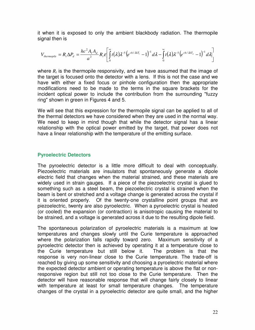
22
it when it is exposed to only the ambient blackbody radiation. The thermopile signal then is
( ) ( ) ( ) ( )
−−−=∆= ∫ ∫
∞ ∞−−−−
0 0
1/51/5
2
2
11 λλλλλλε λλdetdetR
a
AAhcPRV at kTchkTch
t
dl
dtthermopile
where Rt is the thermopile responsivity, and we have assumed that the image of the target is focused onto the detector with a lens. If this is not the case and we have with either a fixed focus or pinhole configuration then the appropriate modifications need to be made to the terms in the square brackets for the incident optical power to include the contribution from the surrounding "fuzzy ring" shown in green in Figures 4 and 5.
We will see that this expression for the thermopile signal can be applied to all of the thermal detectors we have considered when they are used in the normal way. We need to keep in mind though that while the detector signal has a linear relationship with the optical power emitted by the target, that power does not have a linear relationship with the temperature of the emitting surface.
Pyroelectric Detectors
The pyroelectric detector is a little more difficult to deal with conceptually. Piezoelectric materials are insulators that spontaneously generate a dipole electric field that changes when the material strained, and these materials are widely used in strain gauges. If a piece of the piezoelectric crystal is glued to something such as a steel beam, the piezoelectric crystal is strained when the beam is bent or stretched and a voltage change is generated across the crystal if it is oriented properly. Of the twenty-one crystalline point groups that are piezoelectric, twenty are also pyroelectric. When a pyroelectric crystal is heated (or cooled) the expansion (or contraction) is anisotropic causing the material to be strained, and a voltage is generated across it due to the resulting dipole field.
The spontaneous polarization of pyroelectric materials is a maximum at low temperatures and changes slowly until the Curie temperature is approached where the polarization falls rapidly toward zero. Maximum sensitivity of a pyroelectric detector then is achieved by operating it at a temperature close to the Curie temperature but still below it. The problem is that the response is very non-linear close to the Curie temperature. The trade-off is reached by giving up some sensitivity and choosing a pyroelectric material where the expected detector ambient or operating temperature is above the flat or non- responsive region but still not too close to the Curie temperature. Then the detector will have reasonable response that will change fairly closely to linear with temperature at least for small temperature changes. The temperature changes of the crystal in a pyroelectric detector are quite small, and the higher
23
order or non-linear terms can be neglected, at least for reasonable excursions in the intensity of the incident radiation.
A pyroelectric detector is made by taking a thin slice of the material, thermally isolating it and exposing it to the incident radiation. Lithium tantalate, LiTaO3, is one of many materials used for pryoelectric detectors. Electrodes are attached to the opposing faces of the crystal so that the voltage across them can be measured. In the same way as the thermopile, the temperature of the pyroelectric crystal when it is exposed to incident radiation comes to equilibrium in concert with the rate at which energy is absorbed from the incident radiation and conducted to the ambient. Unlike the thermopile the pyroelectric detector cannot be operated under static conditions. This is because the charge generated on the crystal surfaces is neutralized by ions in the surrounding atmosphere or by electrical conduction across the surface of the material. This neutralization can be reduced by careful cleaning and evacuation of the surrounding atmosphere (and perhaps replacement by an inert gas). However, it can never be completely eliminated, and the radiation incident on a pyroelectric detector must be modulated or discontinuously changed. The static radiation incident on the detector is not always completely the ambient radiation. In a room there might be sunlight coming in through a window and reaching the detector by reflection if it is not directly incident on it. In any case, the surface charge generated by the incident radiation, whatever it is, is soon neutralized, and the detector signal drops to zero.
The pryoelectric detector is frequently used as a motion sensor. In this case, a solid angle or field-of-view directed at some portion of a room or outside environment is focused onto the detector. This solid angle is typically filled with the ambient temperature radiation field. When the target moves into the detector's field-of-view some portion of the ambient radiation is replaced by radiation emitted by the target changing the temperature of the detector crystal. Again as with the thermopile, the detector signal is positive if the target temperature is above the ambient and negative if it is lower. No chopper is needed for a motion detector since the change in incident radiation is provided by the movement into and out of the detector's field-of-view.
A detector signal is generated whenever the crystal's temperature is changed whatever the cause. Drifts in the ambient temperature can then interfere with detection of changes in the incident radiation. This issue can be addressed by connecting an identical but blind detector either in series or parallel opposition with the detector exposed to the incident radiation. Both detectors equally track the ambient temperature, and the signals generated by an ambient temperature change cancel each other since the two detectors are connected with opposing polarity. The optical signal, however, generates a signal in only one detector since the other is blind. The second detector is frequently made blind by mounting the optically active detector on top of it.
A pyroelectric detector can be operated in either of two modes.
24
• Voltage Mode Operation - Electrodes are placed on opposing faces of the pyroelectric crystal, and the voltage generated between the electrodes is measured without drawing any current. The surface charge is so small at the relatively low modulation frequencies used for voltage mode operation that it will be quickly neutralized if any current is allowed to flow. The input impedance of many currently available instrumentation and operational amplifiers is sufficient to allow the detector voltage to be measured directly. Frequently, the electrode connected to the exposed pryoelectric surface is connected to the gate of a field-effect-transistor (FET) mounted within the enclosure or detector package to provide the needed electrical isolation. The temporal response of a typical detector increases with frequency to a peak somewhere in the vicinity of 0.01 Hz and then starts to slowly fall off due to the thermal mass of the detector material. This fall- off is fairly slow up to 5-10 Hz when the response starts falling rapidly to unusable levels since there is insufficient time to bring the detector material to a uniform temperature.
• Current Mode Operation - While the surface charge generated on a pyroelectric crystal is small, it is large enough to be measured. This is accomplished by shorting both electrodes to the same potential level (typically circuit common) and measuring the current that flows on and off the exposed crystal face. If the incident radiation is suddenly increased, that radiation is absorbed at the exposed surface of the crystal and is initially concentrated in a thin layer just below the surface. The temperature of the crystalline material in this layer is temporarily increased. This absorbed energy is then thermally conducted into the bulk of the material, but the thermal conduction process is inherently slow. The energy then is initially contained within a fairly small thermal mass under non-equilibrium conditions, and the temperature of this material is significantly increased thereby generating a significant surface charge on the exposed crystal face. With time the absorbed energy is thermally conducted into the bulk of the crystal, and the surface charge of the exposed face is decreased. However, if the incident radiation is modulated at a rate high enough that thermal conduction is not a significant dynamic factor, this non-equilibrium condition can be maintained, and the surface charge on the exposed face is modulated at a significant and measurable level. By grounding both electrodes electrostatic forces are eliminated, and the current required to neutralize the surface charge can be measured. For most pyroelectric detectors operated in the current mode, the response is fairly stable at high frequencies, starts to fall off at frequencies below 10 Hz and becomes unusable for modulation frequencies much below 5 Hz.
If a mechanical or electronic chopper at the ambient temperature is used to observe a static target, the above expression for the thermopile signal can be used for the pryoelectric detector since it is only the change in incident radiation that matters. The same is true if the detector is used as a motion sensor where
25
the target walks into the sensor's field-of-view blocking the ambient radiation that comes from behind. If the radiation the target blocks is not all ambient radiation but includes something else such as sunlight for example, the appropriate corrections must be included. Otherwise, the above expression for the thermopile signal can be used with the appropriate pryoelectric detector responsivity. The voltage mode and current mode responsivities have the units of V/W and A/W, respectively. As mentioned above the detector responsivity in either mode has a definite temporal dependence, and one must use the value of the responsivity that corresponds to the rate at which the incident radiation is changing.
Bolometers
The bolometer was the first infrared detector. Basically, it is just a resistor that is thermally isolated and exposed to the incident radiation. The bolometer temperature changes with the net rate at which it absorbs the incident radiation, and the resistance of the device changes as well. This resistance change is measured by passing a small current through the bolometer and measuring the voltage across it or in extreme cases using a Wheatstone bridge where no current flows when the bridge is in balance.
The bolometer is probably the most straightforward thermal detector to examine. The electrical resistance of a conductive material increases slowly and in a very non-linear fashion at low temperatures but then curves upward and becomes very linear with temperature when the material's temperature rises above 20% or so of the material's Debye temperature where we enter the domain of classical physics from the domain of quantum physics. Since the Debye temperatures are typically in the range of a few hundred Kelvins, nonlinearity of a bolometer's resistance only becomes a concern when it is operated at cryogenic or at least refrigerated temperatures. It is the change in the bolometer's resistance with the change in absorbed optical power that we are normally concerned with. The two are proportional, at least under the right conditions, since linearity carries through from power to temperature to resistance.
Bolometers are now finding fairly wide use in thermal imaging. Thermally isolated resistor elements, called microbolometers because of their small size, are deposited on each cell of an integrated circuit. The number of cells (or pixels for picture element) can be quite large in a typical imager, up to several hundred thousand, and megapixel arrays are being developed for military applications. The circuitry in each cell senses the microbolometer resistance and outputs that information to the imaging electronics that generate the high resolution thermal image. Other types of detectors, particularly the photodiode, are used in thermal imaging application as well, often with a higher level of performance, but the microbolometer is emerging as the cost effective approach for many applications primarily because cryogenic cooling is not required. However, temperature stabilization of the microbolometer array is usually necessary.
26
The temperature and, therefore, the resistance of each microbolometer element changes in direct proportion to the rate at which optical energy is absorbed by that element. There are a couple of problems with using the microbolometer array for thermal imaging. The first is when the contrast in the scene is very small; the amounts of radiation coming from different parts of the scene differ very little from one another compared to the average over the scene. Also, the resistances of the microbolometer elements vary enough so that the voltage signals coming from the array elements vary much more due to the variations in resistance than spatial variations in the incident radiation. The thermal image gets washed out or buried by these resistance variations. Cell-to-cell threshold variations in the readout chip also introduce substantial offset variations from one pixel to the next. These issues are addressed by exposing the imager successively to two uniform scenes corresponding to two temperatures and capturing an image or frame of each. The two frames are then used to calculate two point corrections (gain and offset) for each pixel. These correction coefficients are stored in memory and used by a microprocessor in the camera electronics to correct the signal from each microbolometer element. The corrections must be applied to each image frame that is captured.
The microbolometer array could be used in this way as a starring thermal imaging array if it were not for 1/f noise. If a microbolometer array is used to image a static scene, one initially sees an excellent thermal image after the pixel- by-pixel offset and gain corrections have been applied. However, after several minutes the image begins to deteriorate with some detectors randomly increasing in signal while others randomly decrease. After a while the image fades away completely. The cause is 1/f nose, and there is no cure. To get around the problem the array is periodically exposed to a uniform ambient radiation field, usually by closing a shutter. This scene is captured by the camera electronics and is subtracted from each frame read out from the array following the opening of the shutter until the shutter is again closed a few minutes later to capture the next reference frame. Basically, this is just updating the offset correction for each pixel. In this way the 1/f noise is not allowed to build up to the point where it significantly impacts image quality. The dynamic offsets caused by 1/f noise are generally much smaller than the static offsets introduced by threshold variations in the readout chip. Perhaps a more accurate statement is that the dynamic offsets are not allowed to become that large before reset occurs.
The issue is the same whether we have an array of microbolometers or a single bolometer element. This subtraction of the reference frame, or reference signal in the case of a single detector element, brings us back to the difference between the incident radiation and the ambient blackbody radiation and to the above equation for the thermopile.
27
Ferroelectric Detectors Like microbolometers ferroelectric detector arrays were developed for thermal imaging applications. The most commonly used material is barium strontium titanate, BaSrTiO3. The material undergoes a ferroelectric phase change at a temperature a bit below room temperature. An array of BaSrTiO3 detectors hybridized to a silicon readout chip is mounted on a thermoelectric cooler that maintains the array at a nominal temperature just below the phase transition. The incident radiation then warms or cools the temperatures of the individual detector elements just a bit above or below the nominal temperature. The ferroelectric material is placed between two plate-like electrodes forming a capacitor. Since the detector is operated on the edge of the phase change, the material's dielectric constant undergoes dramatic changes with temperature causing substantial changes in the capacitances of the individual detector elements. The capacitance changes are detected by the cells of the readout chip and formed into a thermal image.
This type of array requires a mechanical chopper. The electronics captures a frame when the chopper is closed corresponding to the ambient radiation field and a second frame when the chopper is open corresponding to the target scene. The two frames are subtracted by the electronics to provide the output image. This brings us back to the difference between the target scene and the flat scene ambient and again to the above expression for the thermopile. While the pixel-by-pixel offsets are corrected automatically by subtracting the chopper open and closed frames, the capture of a flat frame or uniform image corresponding to a temperature substantially different from the ambient is needed to provide correction for variations in the nominal detector capacitance values and the electronic gains of each cell. The microprocessor embedded in the sensor electronics applies this "gain" correction to each pixel. Quantum Detectors In thermal detectors the incident radiation is absorbed by the detector material and is manifested as an increase in its temperature. The situation is different with quantum detectors where the detector is normally maintained at a constant temperature. A quantum detector is made from a semiconductor, and the incident radiation excites electrons from the semiconductor's valence band to the conduction band. To understand what is going on we first have to understand something about semiconductor energy bands.
First, we have to discuss atoms for a bit. The electrons in an atom are quantized into energy levels (for those of you keeping track, this is first quantization). We are used to thinking of these energy levels in terms of Bohr orbits of the electrons around the nucleus. In quantum mechanical terms electrons are Fermions, and no two interacting Fermions can be in exactly the same energy state, or have the same set of quantum numbers. When atoms condense into a solid, the
28
outermost or valence electrons interact strongly. Actually, the valence electrons bind the atoms together. When the atoms are far apart, corresponding electrons in the atoms have essentially the same energy. As the atoms come into proximity, the electrons apply electrostatic forces on one another, and the individual energy levels of each atom are shifted by small amounts, different for each atom. The discrete energy levels of the atoms then are spread out into quasi-continuous bands with some 1023 individual energy levels in each band with the bands corresponding to the energy level structure of the undisturbed atom. Sometimes the bands overlap and sometimes there is a gap between them where no energy levels exist.
In a metal the valence electrons disassociate from the individual atoms and become part of the material as a whole. They are free to move though the material and conduct an electrical current in response to an applied voltage. The energy band containing these electrons is not full. There is no gap between the states of the highest energy electrons, those at what is called the Fermi energy, and the adjacent sea of unoccupied states. An electron with the slightest provocation can move into another state and through the material.
In an insulator the valence electrons are actually locked tightly into the bonds between adjacent atoms. In terms of band theory, the valence electrons completely fill a band, and a large gap exists between the top of the valence band and the bottom the next band, called the conduction band. In an insulator the conduction band is nominally empty, has no electrons. In order to excite an electron to the conduction band, a substantial amount of energy must be given to a valence electron to break it loose from the bond which is exerting a strong attractive force on that electron. In an insulator very few electrons are in the conduction band, and the material is a poor conductor of electricity and heat. Thermal energy in the material, the phonons, will always excite some electrons to the conduction band, but in an insulator this number is very, very small.
In a semiconductor an energy gap between the valence and conduction bands exists as in an insulator but is smaller. A semiconductor such as silicon is held together by covalent bonds. In its cubic crystalline structure each silicon atom has four outermost or valence electrons and four other silicon atoms that are closest to it. Each silicon atom donates one of its valence electrons to the bonds with the adjacent atoms. A covalent bond between two atoms then consists of two electrons, one from each atom. The electrons are not as tightly bound as they are in insulators and can be broken loose by absorbing the energies of either photons or phonons, incident radiation or the indigenous thermal energy of the material. At a finite temperature a semiconductor always has a not insignificant number of conduction electrons that have been thermally excited across the band gap or broken loose from their bonds. As the temperature of the material is increased, more electrons are excited across the band gap to the conduction band. Unlike a metal, the electrical conductivity of a semiconductor increases with temperature as more electrons are added to the conduction process.
29
Conduction electrons can also be added to a semiconductor by doping. In doping, impurity atoms are used to replace a small fraction of the normal atoms in the crystal structure. In silicon, if another atom with four valence electrons, such as germanium, is used, nothing much happens. However, if an atom such as phosphorus or arsenic with five valence electrons is used as the dopant, the fifth valence electron is left without a bond. The extra electron is weakly attracted to its parent nucleus by electrostatic forces, but with any thermal agitation at all it breaks loose and becomes a conduction electron. These doping electrons provide a conductivity floor that is nominally independent of temperature except at very low temperatures where they tend to be "frozen out" (at these low temperatures there are no longer phonons with sufficient energy to overcome the electrostatic forces applied by the host nuclei). Semiconductors that are doped with extra valence electrons are called n-type.
Dopants with fewer valence electrons than the host may also be used. In the case of silicon this might be boron which has only three. In this case, there is a bond left short an electron. The covalent bond with only one electron is called a hole. It can also conduct electricity. The hole applies an attractive electrostatic force on the electrons attached to the complete bonds in its vicinity. If an electric field is applied to the material, the added inducement will cause an electron to jump from an adjacent bond to the hole completing that bond but leaving the hole behind on the bond it came from. The hole then moves in the opposite direction of the electron current (that is, in the direction of the electric field) and acts like a positive charge carrier. A hole is generally less effective in carrying an electrical current than an electron in the conduction band. In order for a hole to move it must pull an electron off of an adjacent bond that is trying to hold on to that electron while the conduction band electron is more or less free to move around. The conduction electron is said to have a higher mobility than the hole. Semiconductors with dopants that are short valence electrons are called p-type. Doping, both n-type and p-type, will be important when we discuss photoconductive detectors and photodiodes.
Aside from doping and absorption of phonons, electrons can be excited to the conduction band by absorbing photons, which is the way radiation is detected. The band gap between the valence and conduction bands has a well defined energy. In order to be absorbed, the photon must have enough energy to break the electron loose from its bond and excite it to the conduction band. Since there is effectively a continuum of energy states above the band gap, those photons with energy equal to or greater than the band gap energy are able to excite valence electrons while those with energy less than this are not and do not cause an increase in the number of electrons in the conduction band. Only radiation with wavelength shorter than a critical value can generate conduction electrons. This critical wavelength is given by
gc Ehc /=λ
30
where Eg is the energy across the bandgap (remember our earlier formula for the energy of a photon). The bandgap energy varies from material to material. Silicon can detect radiation with wavelengths less than 1.1 µm. It is the standard detector for visible radiation, and essentially all television cameras use silicon detector arrays. However, unless it is doped with specific impurities to insert localized states within the bandgap, silicon does not detect infrared radiation, at least at wavelengths much longer than NIR. Lead sulfide detects radiation with wavelengths less than 3 µm and is a good SWIR detector. Lead selenide and indium antimonide detect radiation less than 5 µm and are good MWIR detectors. Silicon carbide, on the other hand, has a fairly wide bandgap and makes a good ultraviolet and X-ray detector. We should note that when an electron is excited from the valence band to the conduction band, two charge carriers are generated, the electron in the conduction band and a hole in the valence band. The combination is usually called an electron-hole pair.
As Eg is reduced, more and more electrons are excited to the conduction band by thermal agitation. This is a significant source of noise since these thermally generated charge carriers are dumped on top of the signal generated by the radiation. Wide bandgap detectors like silicon and even lead sulfide can be operated at room temperature without ill effect unless exceptionally low levels of radiation are being detected. The performance of narrower bandgap detectors such as those used for MWIR and LWIR detection are almost always improved by cooling. Thermoelectric coolers can often be used to refrigerate some but not all MWIR detectors to -40o C or so with good effect. Some MWIR and nearly all LWIR detectors require cryogenic cooling to the vicinity of liquid nitrogen temperature (78 K). Wide band gap detectors such as those used for ultraviolet and x-rays usually do not need to be cooled except in cases where they are being used to detect very low levels of radiation. As a general rule, the best performance is achieved by using a detector with the widest bandgap that still allows detection of the radiation wavelengths of interest.
Quantum detectors are normally mounted directly on a heat sink, frequently at a reduced temperature, and the detector temperature does not change with the incident radiation. In a quantum detector the incident photon is absorbed by an electron in the valence band of the semiconductor material exciting that electron into the conduction band if the photon has enough energy to do so. If not, the photon is simply not absorbed, at least by the valence electrons. The electron is excited into an energy state that is above the bottom of the conduction band by an amount equal to the photon energy minus the gap energy, Eg. The excited electron rapidly falls to the bottom of the conduction band giving up the excess energy as heat generating phonons in the detector material that are absorbed by the heat sink. It is the conduction electron that we detect, and it is clear that we get one conduction electron for each photon absorbed. Some of the conduction electrons recombine with holes before they make it across the detector to our electronics. We then end up with fewer conduction electrons than we had photons with sufficient energy to generate them. The ratio of detected
31
electrons to photons is called the quantum efficiency and is always less than unity.
If we counted photons, the responsivity would be a constant for all wavelengths shorter than the cutoff wavelength, λc, and fall to zero for all wavelengths longer than λc. However, we generally give responsivity in terms of incident power rather than photon flux. The responsivity of a quantum detector then has a maximum value actually just a bit below the cutoff wavelength (due to the finite detector temperature) and decreases as the wavelength decreases since the number of photons per watt decreases as the wavelength decreases. The measured responsivity for an InGaAs photodiode is shown in Figure 6. The tail at longer wavelengths is due to thermal broadening of the energy bands, and the ripple at shorter wavelengths is due to spectral interference in the antireflection coating on the photodiode surface. The values of responsivity quoted for quantum detectors are usually those at the peak, but one must be careful of what is meant by the numbers since they do change with wavelength.
We have enough understanding of the basic issues that we can now discuss quantum detectors. There are two common types, photoconductors and photodiodes
Photoconductors Photoconductors are made from semiconductors that have been heavily doped n-type or p-type and are frequently used for infrared detection. Detectors made from these materials have a finite electrical conductivity that increases with temperature. The resistance of an infrared photoconductive detector can be as little as 10 Ω or as much as 10 MΩ. When these detectors are exposed to radiation, additional conduction electrons and holes are generated and the detector resistance is reduced. However, the change is not much, usually less than 1% for normal radiation intensities.
Photoconductive detectors are usually operated by biasing them with a fixed voltage and measuring the current flowing in the biasing circuit. The current in the absence of radiation is called the dark current. The photo-signal is the increase in current when the detector is exposed to radiation. Since the bandgaps of infrared detectors are relatively small, a substantial number of electrons are thermally excited to the conduction band. A small increase in the detector temperature can in most cases excite an additional number of electrons
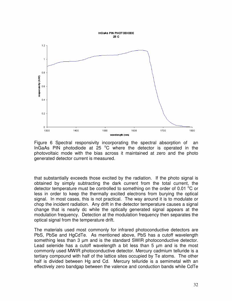
32
Figure 6 Spectral responsivity incorporating the spectral absorption of an InGaAs PIN photodiode at 25 oC where the detector is operated in the photovoltaic mode with the bias across it maintained at zero and the photo generated detector current is measured.
that substantially exceeds those excited by the radiation. If the photo signal is obtained by simply subtracting the dark current from the total current, the detector temperature must be controlled to something on the order of 0.01 oC or less in order to keep the thermally excited electrons from burying the optical signal. In most cases, this is not practical. The way around it is to modulate or chop the incident radiation. Any drift in the detector temperature causes a signal change that is nearly dc while the optically generated signal appears at the modulation frequency. Detection at the modulation frequency then separates the optical signal from the temperature drift.
The materials used most commonly for infrared photoconductive detectors are PbS, PbSe and HgCdTe. As mentioned above, PbS has a cutoff wavelength something less than 3 µm and is the standard SWIR photoconductive detector. Lead selenide has a cutoff wavelength a bit less than 5 µm and is the most commonly used MWIR photoconductive detector. Mercury cadmium telluride is a tertiary compound with half of the lattice sites occupied by Te atoms. The other half is divided between Hg and Cd. Mercury telluride is a semimetal with an effectively zero bandgap between the valence and conduction bands while CdTe
33
is a fairly wide bandgap semiconductor. The bandgap of HgCdTe can be adjusted continuously by varying the relative concentrations of Hg and Cd. If the Hg/Cd half of the material is 30% Cd and 70% Hg, the cutoff wavelength is around 5 µm making the detector sensitive to MWIR. If the concentrations are 20% Cd and 80% Hg, the cutoff wavelength is about 10 µm making an LWIR detector. Since PbS and PbSe are available and less expensive, they are usually used for shorter wavelength detection. However, cryogenically cooled HgCdTe has higher performance and is used for shorter wavelength detection when that performance is needed. Mercury cadmium telluride is the standard LWIR photoconductive detector.
Photoconductors are frequently, but not always, polycrystalline materials. That is, instead of being one big single crystal, the detector is made up of a number of smaller crystals. In a crystal, the atoms have an orderly geometric arrangement. A grain boundary is the transition region between a crystal of one orientation of that geometric arrangement and an adjacent crystal with a different orientation. The orderliness of the atomic arrangement breaks down within the grain boundary. Since band theory requires the orderly arrangement of the atoms, the concept breaks down and the band gap goes away. However, the performance of a photoconductive detector is still well described by band theory as long as the grain boundaries make up the small part and good crystals the large part of the material. This will not be the case when we discuss photodiodes.
Photoconductors are highly doped so they have a high concentration of charge carriers in the absence of any incident radiation, either electrons in the valence band or holes in the conduction band. If the incident radiation has enough energy to bridge the bandgap, it excites electrons to the valence band, leaving behind hole in the valence band. Typically the number of excited charge carriers is significantly less than 1% of the number that is already there through the doping. We then have the problem of separating the small number from the large number. Also, electrons are thermally excited across the band gap, and, unless, the detector temperature is very tightly controlled that number can also be much larger than the number excited by the radiation. A constant voltage is applied across the photoconductive detector, and the current is measured to determine the total number charge carriers present. The way to separate the radiation generated charge carriers from the rest is to mechanically chop the incident radiation. When the chopper is closed the signal is what is generated when the target object is replaced by the ambient including the signal from the doping charge carriers, any thermally generated charge carriers as well as those from radiation emitted from the surrounding objects including a cold shield if there is one as well as the objects at the ambient temperature. When we open the chopper we replace the ambient radiation corresponding to the field-of-view occupied by the target with the radiation emitted by the target as well as the ambient radiation reflected by the target. The result is similar to what we had above for the thermopile except that the signal is now a difference current instead of a voltage and the responsivity has a spectral dependence and must be included in the integration.
34
( ) ( ) ( ) ( ) ( ) ( )
−−−=∆ ∫ ∫
∞ ∞−−−−
0 0
1/51/5
2
2
11 λλλλλλλλε λλdeRtdeRt
a
AAhcI at kTch
c
kTch
c
dl
ctorphotocondu
where Rc(λ) is the material's photoconductive responsivity in A/W Photodiodes A diode consists of a single crystal semiconductor where a portion has been doped p-type and the remainder n-type or visa versa. The electrons in the conduction band on the n-side will tend to drift across the junction between the two sides and combine with the holes on the p-side. That is, the conduction band electrons from the n-side will cross over to the p-side and be captured by the bonds that are short an electron. This will not continue indefinitely. Both sides of the junction are normally electrically neutral. When the conduction electrons cross over they leave the n-type material in the vicinity of the junction with a net positive charge and generate a net negative charge on the p-side. This residual charge keeps any more electrons on the n-side or holes on the p-side from moving toward the junction and stops the process. The region of n-type material in the immediate vicinity of the junction is depleted of conduction electrons, and a similar region in the p-type material is depleted of holes. The combined region from both sides is called the depletion region. A potential difference called the contact potential is generated across the junction.
Additional charge carriers are generated when a photodiode is exposed to radiation with wavelength short enough to bridge the bandgap. The increased density of charge carriers causes more electrons from the n region to cross over and combine with holes in the p region until electrostatic forces again stop the process. This causes the depletion region to widen and the potential across the junction to increase. If no current is allowed to flow through the diode, a voltage is generated across it that is logarithmically dependent on the radiation intensity. This is called the open circuit condition, and the voltage across the junction is called the open circuit voltage, Voc. The detector can also be operated in the short circuit condition. Here the two sides of the detector are shorted together so that no voltage is allowed to develop across the diode. In order to keep the voltage from developing, the charge carriers being generated by the radiation and crossing the junction must be continuously removed from one side of the diode and sent back to the other. In other words, current flows through the diode that is proportional to the incident intensity. This current is called the short circuit current, Isc. The I-V curves for a photodiode both in the dark and illuminated with incident radiation are shown in Figure 7, and Voc and Isc are indicated.
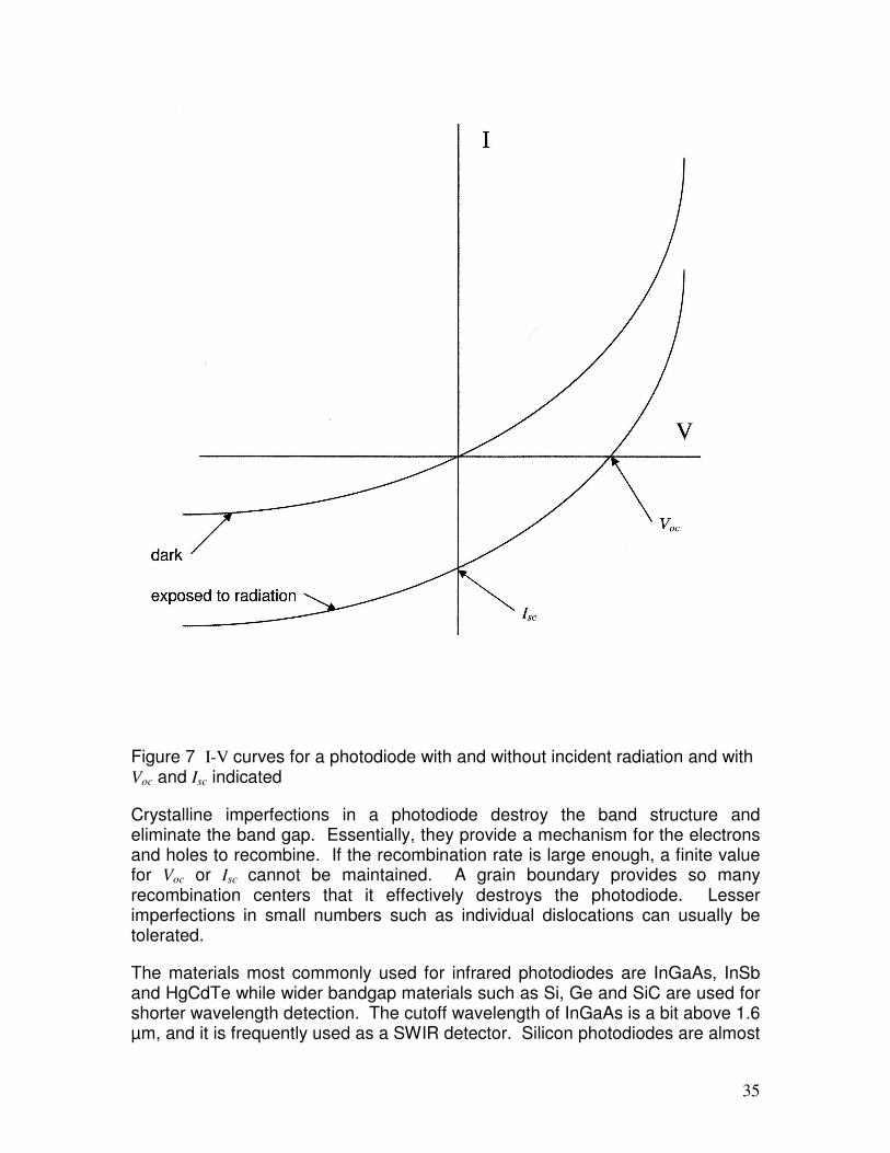
35
Figure 7 I-V curves for a photodiode with and without incident radiation and with Voc and Isc indicated
Crystalline imperfections in a photodiode destroy the band structure and eliminate the band gap. Essentially, they provide a mechanism for the electrons and holes to recombine. If the recombination rate is large enough, a finite value for Voc or Isc cannot be maintained. A grain boundary provides so many recombination centers that it effectively destroys the photodiode. Lesser imperfections in small numbers such as individual dislocations can usually be tolerated.
The materials most commonly used for infrared photodiodes are InGaAs, InSb and HgCdTe while wider bandgap materials such as Si, Ge and SiC are used for shorter wavelength detection. The cutoff wavelength of InGaAs is a bit above 1.6 µm, and it is frequently used as a SWIR detector. Silicon photodiodes are almost
36
always used for the detection of NIR and visible wavelengths. Both InSb and HgCdTe must be refrigerated to provide any sort of reasonable performance, while the bandgap of InGaAs is wide enough that cooling below room temperature is usually not needed. Both InSb and HgCdTe operate best at cryogenic temperatures, 80 K and below. The cutoff wavelength of InSb is about 5.5 µm, and InSb can be used for MWIR detection. Its performance falls off rapidly with increasing temperature and is really not useful much above 90 K. The cutoff wavelength of HgCdTe can be adjusted continuously throughout the infrared spectrum. The performance of HgCdTe also degrades with temperature albeit more slowly. Mid-wave HgCdTe provides useful performance at temperatures as high as 160 K. Long wavelength HgCdTe must be cooled below 80 K. Mercury cadmium telluride is the standard LWIR detector and is frequently used for MWIR detection with λc on the order of 5 µm and even less, although InSb is used more commonly. At cryogenic temperatures both InSb and HgCdTe offer the highest level of performance available today in these spectral regions. The use of liquid nitrogen is the least expensive way to cool the detectors to these temperatures but is too awkward for many applications. The development of compact Stirling cycle cooling engines in recent years provides an affordable if still somewhat expensive alternative. The wider bandgaps of the detectors used for visible, ultraviolet and x-ray detection reduces the thermal generation of charge carriers to the point where cooling of the detector is not necessary except in cases of detection of very low levels of radiation. Photodiodes are absolute detectors, the detector signal depends on the total radiation incident on it. Choppers are not normally used with photodiodes, but cold shields frequently are used. If a cold shield is not used such as with a room temperature operated InGaAs photodiode, the current signal for operation in the photovoltaic (short circuit) mode is given by
( ) ( )∫∞
−− −=0
1/5212 λλλπ λ
deRAhcI akTch
Idphotodiode
( ) ( ) ( ) ( ) ( ) ( )
−−−+ ∫ ∫
∞ ∞−−−−
0 0
1/51/5
2
2
11 λλλλλλλλε λλdeRtdeRt
a
AAhcat kTch
I
kTch
I
dl
where RI(λ) is the photovoltaic responsivity in A/W. If the detector is operated in the open circuit mode, the result is similar except the signal is a voltage.
( ) ( )∫∞
−− −=0
1/5212 λλλπ λ
deRAhcV akTch
Vdphotodiode
( ) ( ) ( ) ( ) ( ) ( )
−−−+ ∫ ∫
∞ ∞−−−−
0 0
1/51/5
2
2
11 λλλλλλλλε λλdeRtdeRt
a
AAhcat kTch
V
kTch
V
dl
37
where RV(λ) is the open circuit responsivity in V/W.
Cold shields are almost always used with cryogenically cooled photodiodes such as InSb and HgCdTe. In this case, the ambient radiation is blocked out by the cold shield except for that part reflected by the target. For a cold shielded photodiode operated in the photovoltaic mode, the detector signal is given by
( ) ( ) ( )∫∞
−− −=0
1/5
2
2
1 λλλλε λdeRt
a
AAhcI tkTch
I
dl
photodiode
( ) ( ) ( ) ( )∫∞
−− −−+0
1/5
2
2
11 λλλλε λdeRt
a
AAhcakTch
I
dl
( ) ( ) ( )∫∞
−− −
−+
0
1/521
212 λλλλ
π
φπ λ
deRtAhc skTch
Id
where as beforeφ is the solid angle subtended by the cold shield aperture as
seen from the detector and Ts is the cold shield temperature. Usually Ts is so small that the last term can be neglected. The extension to a cold shielded photodiode operated in the open circuit mode should be clear.
LWIR HgCdTe photodiodes are often operated at a small reverse bias rather than in the true photovoltaic condition. This moves the operating point to the left and out to a flatter portion of the I-V curve shown in Figure 7. This increases the detector's dynamic resistance reducing its Johnson noise. However, it also introduces some dark current, current added to Isc, and the concomitant shot noise. The amount of reverse bias that is applied is selected to minimize the sum of the Johnson and shot noises. This is typically in the range of 10-20 mV. As discussed below, the Johnson and shot noise contributions are statistically independent and are added in quadrature.
DETECTOR FIGURES OF MERIT
As we have said, electro-optic detectors can broadly be put into two categories, semiconductor detectors that have a bandgap that can be bridged by the incident radiation and non-semiconductor detectors where a bandgap is not relevant. As mentioned above, semiconductor detectors are often referred to as quantum detectors and non-semiconductor detectors as thermal detectors. Both types are usually characterized by the same or similar figures of merit. The figures of merit for the quantum detectors will often have a spectral dependence while this generally is not the case for thermal detectors.
38
• Responsivity The responsivity, R, is the ratio of output to input. The input is usually taken to be the optical power incident on the detector. In the real world the detector responds to the optical power it absorbs, and as we have discussed, the incident power and the absorbed power are generally not quite the same thing due to reflection at the detector surface. Often the absorbed power is a simple fraction of the incident power but not always, and one must be careful. Since the reflected power falls to zero for normal incidence and except for short focal length optical systems the incident radiation is directed onto the detector at near normal incidence, the manufacturer's stated responsivity (for normal incidence) will be assumed to be appropriate except for extreme or unusual situations. If a higher degree of accuracy is needed, a detailed analysis of the optical system will be required with integration over the angular spread of the incident rays taking into account the absorbed and reflected components of each ray. The output depends on the type of detector but is usually either a voltage or a current, and responsivity usually has the units of volts per watt or amps per watt.
o A thermal detector only cares about how much energy it absorbs and not what wavelengths the photons had that carried that energy to it. The responsivity of a thermal detector then does not have any spectral dependence, since it is given in terms of incident power and not in terms of the number of incident photons, and is treated as just a number.
o When incident photons have enough energy to be absorbed in a semiconductor detector, that energy is absorbed by the valence electrons allowing them to break loose from their bonds and excite to the conduction band. If the photons do not have enough energy, they are not absorbed (at least by the valence electrons) and the number of charge carriers does not increase. The responsivity of such a detector is proportional to the rate of increase in the number of these charge carriers with incident radiation intensity. If the responsivity is plotted against wavelength, it will be zero for long wavelengths, rise up sharply at λc and then fall slowly for shorter wavelengths. This fall is an artifact of the units we use. Each absorbed photon normally generates one conduction electron even if it has more energy than the minimum necessary, Eg. Since we measure responsivity in terms of the rate at which energy is incident on the detector instead of the number of photons, it falls off at shorter wavelengths where the photons have more energy than they need and that extra energy is not used to excite more conduction electrons but rather ends up generating more phonons.
• Noise All detectors exhibit a noise component called white noise that has uniform temporal spectral power density. Many detectors have an additional noise component called 1/f noise that has a spectral power
39
density that depends inversely on the frequency. Detection is made over a frequency range usually called the detection or noise bandwidth, and the total noise detected with the signal is the total noise spectrum integrated over that band width. The signal-to-noise ratio is increased by reducing the bandwidth as much as possible, usually by filtering. Since 1/f noise decreases with increasing frequency, the signal-to-noise ratio is maximized by detecting at a frequency high enough that the 1/f noise can be neglected.
o White Noise White noise is really simple to deal with. Its spectral power density has a constant value. The total white noise then is this value times the detection bandwidth. As far as white noise is concerned, it doesn't matter what detection frequency is used, only the bandwidth. The signal from a detector is usually given in terms of a voltage or current rather than power. The detector white noise then depends on the square root of the noise bandwidth rather than on the bandwidth itself and usually is given in units of V/√Hz or A/√Hz.
o 1/f Noise The 1/f noise component is dominant at low frequencies, decreases with increasing frequency and eventually falls below the white noise floor. The frequency at which the two noise components are equal is called the 1/f knee. This knee is an important parameter in determining the optimum frequency at which to detect radiation. The 1/f noise can be neglected and performance maximized if detection is made significantly above the knee. The 1/f knee can be as low as a fraction of a hertz for some cryogenically cooled photodiodes or as much as several hundred hertz or even more for other types of detectors.
o Noise Equivalent Power The noise equivalent power, NEP, is the
detector noise referred to the optical input or the optical input power that gives a signal-to-noise ratio of unity. NEP is usually measured above the 1/f knee so that only the white noise is measured. The value of NEP then is proportional to the square root of the bandwidth of the electronics used to measure it. Technically, the unit of NEP is the watt. However, in order to avoid the necessity of also quoting the electronics bandwidth used when it was measured, NEP is often (nearly always?) quoted in units of W/√Hz. NEP is determined by dividing the detector noise signal by the responsivity.
• Detectivity The detectivity, D*, is used primarily to characterize infrared detectors and is probably the most important performance parameter for these detectors. In place of detectivity, the performance of the wider bandgap detectors is usually characterized by the rms open circuit noise voltage. The detectivity is given by
40
NEP
fAD
nd ∆=∗
where
Ad is the optically sensitive area of the detector, as before ∆fn is the bandwidth of the detection electronics
To make things confusing, the term "detectivity" was originally applied to D
= 1/NEP. The distinction is made by the superscript *. The newer D* definition is used because it is nominally independent of the size of the detector and the bandwidth of the measurement circuit while D depends on both. While D* is almost always used and D is seldom if ever used, one should be careful that the proper numbers are being applied. The units of D*are cm√Hz/W. D* is the detector signal-to-noise ratio when 1 W of optical power is incident on the detector, the optical area is 1 cm2 and the noise is measured with a bandwidth of 1 Hz. The detectivity is usually measured above the 1/f knee so that it is independent of the measurement frequency.
o For semiconductor detectors the detectivity is a function of wavelength and is sometimes called the spectral detectivity. It is zero, for example, above λc since the detector generates no signal. The peak value of D* is frequently used and is designated by the subscript λpk. The peak value of D* occurs at a wavelength somewhat below λc.
• Time Constant The time constant, τ, is the time required for the detector to respond to an abrupt change in input optical power. Since a change is reached asymptotically, it is actually the time required for the detector output to reach [1-(1/e)] or 63% of its final change in value. Sometimes this parameter is given in terms of a detection bandwidth, ∆fdet, where ∆fdet = 1/τ. The units of τ are seconds and ∆fdet Hz.
These parameters allow reasonably accurate prediction of the performance that will be achieved with a specific detector.
CHARACTERIZATION MEASUREMENTS
The detector output signal is usually either a voltage or a current. The responsivity is the ratio of the output signal to the input which is usually the incident optical power. The measurement of responsivity is fairly straightforward. A known amount of optical power is directed onto the detector, and the output signal is measured. The responsivity is simply the ratio of the detector signal to the incident power with the units of A/W or V/W. The background
41
contributes to the total power on the detector and must be included. This is sometimes hard to determine. To get around this ac detection is often used. A known amount of flux is generated with a blackbody at a known temperature and with a known aperture. Therefore, the amount of flux reaching the detector from the blackbody is known. A chopper is placed in front of the blackbody and operated at a reasonable frequency, frequently 1 kHz. The difference in optical power incident on the detector when the chopper is open and closed is given by the expression we developed earlier for ∆Pt.
Noise measurements are not quite so obvious. There are usually three contributions to the noise. These are from the detector, the electronics used to make the measurement and the photon flux itself. The incident optical power actually consists of a current of photons with each photon individually striking and being absorbed by the detector. The photon noise is the shot noise, the uncertainty in the number of photons striking the detector which is the square root of that number of photons - this is discussed below. In any case, the three sources of noise are statistically independent and add in quadrature.
222
elecdfluxtot nnnn ++=
where
ntot is the total noise nflux is the shot noise contribution from the photon flux
nd is the noise contribution from the detector nelec is the noise contribution from the detection electronics
As mentioned above, noise is usually measured in A/√Hz or V/√Hz. What we are usually interested in is the detector noise. This is given by
222
fluxelectotd nnnn −−=
In order to determine nd we must know both nelec and nflux in addition to ntot. ntot is the total noise measured when the photon flux or radiation is incident on the detector. The electronics noise is also measured directly by shorting the input leads at the detector.
The shot noise is more difficult as it must be calculated. Shot noise occurs because the incident radiation is quantized into photons. Whenever we have a current of discrete particles flowing into a box, there is always an uncertainty as to how many particles are in the box. There is no reason to go into the statistical analysis and deal with Poisson and Normal distributions. Let us just say that if the box is supposed to have N particles in it, the uncertainty or "noise" in the number actually in the box is √N. The signal-to-noise ratio then due to shot noise is small for small signals and large for large signals. If we have 100 particles in the box, the noise is 10 particles or 10%. If we have 10,000 particles in the box,
42
the noise is 100 particles or 1%. In most cases we are dealing with much larger numbers so the shot noise contribution to the total noise is often quite small.
The shot noise or nflux cannot be measured directly and must be calculated. Since we have setup the structure to calculate the optical power incident on the detector, a minor modification will give us the photon flux incident on the detector. We need to go back to Planck's Law, the expression for the spectral radiant emittance.
( ) 1/5212
−− −= tkTchehcW
λλ λπ
where we have given the temperature of the emitting surface the subscript t to indicate that it is the target that is emitting the radiation. This is the optical power emitted per unit area of the target at wavelength λ. Power is energy per unit time, and if we want to know the number of photons emitted per unit time at the wavelength, we need to divide this by the energy of the photon, E = hc/λ.
( ) 1/412
−− −= tkTch
p ecNλ
λ λπ
We carry this expression through what we have already done to determine the number of photons incident on our detector per unit time. The number of particles in our box is the expression for the photon flux incident on our detector times the sample time τs, the time it takes us to make the measurement or collect the sample. In our analysis τs is just nominal or representative and not a specific sample time. We will end up removing it from our considerations when convert the noise from V or A to V/√Hz or A/√Hz
If Np is the number of photons per second incident on our detector, the number of photons in our sample box so to speak is
sps NN τ=
We obtain Np by carrying the above expression for Npλ through the same process we did for Wλ including the target and ambient temperatures, the solid angle of the limiting aperture, the spectral transmission functions of the objects in the optical path, etc. Then the number of noise photons in our sample is
sps NN τδ =
Then the number of noise photons as a fraction of the total number of photons in our sample is
spss NNN τδ /1/ =
43
Notice that this fraction gets smaller as the number of photons increases, inversely as the square root.
The spectral radiant emittance changes as the temperature of the emitting surface changes, and the optical power incident on our detector must be calculated for each temperature of the emitting surface. The same is true for the number of photons per unit time incident on our detector. However, if we increase the amount of optical power incident on the detector by doubling the lens diameter, for example, again assuming the lens is the limiting aperture, the incident optical power will increase by a factor of 4 since the area of the lens cross section increases by a factor of 4. As well, the number of photons per unit time incident on the detector increases as a factor of 4. The number of photons per second and the optical power incident on the detector for that given target temperature are proportional. Then the noise in the incident optical power for a sample time τs is given by
sp
s
s
s NPN
NPP τ
δδ /==
Since P is a macroscopic or average of a continuously flowing quantity, it doesn't make sense to put the subscript s on it. Now we know that the detector signal is given by
PRS dd =
and then the shot noise on the detector signal due to the discreteness of the incident photon flux is given by
spdspdsdflux NSNPRPRS ττδδ // ===
It is conventional to use the sampling frequency, fs, instead of the sample time where
ssf τ/1=
Then
p
s
dfluxN
fSS =δ
However, it is the usual practice to quote the shot noise as a quantity independent of the sampling frequency.
pdflux NSn /=
44
where Sd is the detector signal and Np is the number of incident photons per unit time. The units of nflux are either V/√Hz or A/√Hz depending on the units of Sd. The actual noise is found just by multiplying by the square root of the sampling frequency.
We usually want to know the noise equivalent power of the detector itself independent of the incident optical power and the detection electronics. Then
R
nNEP d
d =
where
R is, as above, the detector's responsivity Since we have measured ntot and nelec and calculated nflux, we can determine nd.
As mentioned above, the units of Nd are usually A/√Hz or V/√Hz and NEPd usually W/√Hz. The parameter most often used to characterize detector performance is D*, and D* is determined directly from NEPd. In order that D* characterizes the properties of the detector and not the conditions under which it was measured, one needs to be certain that only the detector noise was included in the determination of the value for D*. This is often not the case, and the values quoted for D* are then are not really meaningful, particularly for low noise detectors. The detector's time constant is usually measured with an oscilloscope. A radiation source significantly different from the ambient is placed in front of the detector with a fast shutter in the middle. The detector is exposed to the source radiation when the shutter is open and just the ambient radiation when it is closed. The rise (step increase in radiation) and fall (step decrease in radiation) times are observed on an oscilloscope. The rise and fall times are then determined directly from the oscilloscope traces. The rise and fall times may very well be different, and both should be measured. The oscilloscope trace incorporates the rise and fall times of the electronics as well as that of the detector. If the electronics are not fast enough so that their rise and fall times can be ignored, they will have to be independently measured and analytically extracted from the measurements.
________________________________________________________________
Infrared and Electro-optic Technology Everett Companies LLC Phoenix, Arizona, USA
telephone: 480-706-4753 email: [email protected]


![A GENERALIZED DIVERGENCE FOR STATISTICAL INFERENCEbiru/anb.pdf · A Generalized Divergence for Statistical Inference 5 the form PD λ(dn,fθ) = 1 λ(λ+1) ∑ dn [(dn fθ)λ −1]](https://img.pdfslide.us/doc/110x75/5f651e2163f94e217345983e/a-generalized-divergence-for-statistical-inference-biruanbpdf-a-generalized.jpg)


![K. K. Sharma National Center for Free Radical Research ... · [Ru(phen)2(dicnq)]2+ difference ( % ) , corrected ( ) & parent spectrum ( ) pH 7 , dose/pulse ~ 7 Gy λ max in nm k in](https://img.pdfslide.us/doc/110x75/5ec437efa1639475be378b5a/k-k-sharma-national-center-for-free-radical-research-ruphen2dicnq2.jpg)